$ 0)*%*1-$/ 2$+1*3 )- 4$&&)5'1'&6 7/*8$/&6 +*/ 91$:€¦ · the more...
TRANSCRIPT

Investigation of Lead-free Nanosolder Reflow and Wettability Property for
Electronics/Nanoelectronics Assembly and Packaging
Fan Gao,1 Zhiyong Gu,1,* Sammy Shina,2 Gregory Morose,3 Pamela Eliason3 and Robert Farrell4
1. Department of Chemical Engineering, University of Massachusetts Lowell, Lowell,MA, USA;; * [email protected]
2. Department of Mechanical Engineering, University of Massachusetts Lowell, Lowell,MA, USA
3. Massachusetts Toxics Use Reduction Institute, University of Massachusetts Lowell,Lowell, MA, USA
4. Benchmark Electronics, Nashua, NH, USA
ABSTRACTThe approach of nanosoldering has shown promise
in the construction of functional and interconnectednanostructures from nano-building blocks by utilizingnanosolder reflow processes. However, in such a reflowprocess, the surface oxidation and wettability ofnanosolders are critical factors in the practicalnanosoldering applications. In this study, the usage of avapor phase-based flux process demonstrates the efficiencyof cleaning nanosolder surface oxide and ensuring goodnanosolder reflow. We show the interaction of nanosolderswith metallic surfaces of copper nanowires and substrate.The effect of two industrially relevant fluxes has beenstudied on nanosolder reflow processes. These studiesprovided necessary first-hand knowledge in developing thenanosoldering techniques and their potential applications innanomaterials assembly and nanodevice fabrication.
Keywords: nanosolder, nanowire, reflow, wetting,nanoelectronics assembly
1. INTRODUCTION
The demand for high-performance interconnects inadvanced packaging pushes the dramatic scaling down ofthe electronics packaging feature size from microscale tonanoscale. Novel or enhanced interconnection andpackaging techniques have to be developed to meet avariety of needs for device or system level integration.Nanosolder-based joining and interconnection techniquesprovide a wonderful opportunity to form robust jointsbetween nanostructures and to integrate nanocomponentsinto a functional device or complex system [1].
We envision that nanosolder applications shouldbe classified into at least two types of approaches. Fig. 1 isa schematic representing the possible nanosolder
applications using both approaches. One approach is thedevelopment of nanosolder paste which is an extension tothe conventional solder paste composing of micron-sizedsolder balls (Fig. 1a). The other approach is nanosolderjoint formation between functional nanostructures. Thisincludes the situation of joining nanowires with nanowiresand/or joining nanowires with other structures such ascontact pads (Fig. 1b). Recently different kinds of soldernanoparticles based on tin material such as Sn/Ag [2],Sn/Ag/Cu [3], and Sn/Cu/Bi [4] alloys have beensynthesized and characterized which have been explored asan alternative to the micron-sized solder balls in order toobtain lower melting point of solder materials and avoidcomponent damage [5]. During the reflow process, thenanoparticles will melt and merge together to form a largersolder bump on the substrate, as shown in Fig. 1(a).Although the size dependent effect of nanoparticles hasbeen proven by most simulated studies when the radii ofnanoparticles are less than 20 nm, experimental results didnot bring significant decrease of melting temperature whichmay be due to many factors such as particle agglomeration,surface oxidation, etc [6].
Reflow
Nanoscale solderparticles
Nanosolderbumps
(a)
Nanowire
Nanosolder segment Contact pad
Nanowire
Nanosolder bumps
(b)
Reflow
Figure 1. Schematic of nanosolder assembly and packagingtechniques. (a) Conventional solder paste alternative. (b)Nanojoint formation between nanowire structures.
NSTI-Nanotech 2011, www.nsti.org, ISBN 978-1-4398-7139-3 Vol. 2, 2011422

The more significant need for nanojoint is theformation of nanojoints and/or nanoscale interconnectionsbetween nanostructures, which is a more promisingapproach because the solder segment on the nanowires canbe precisely controlled and effectively joined by a reflowprocess without intensive extra processing [7-8]. Therealized one-dimensional nanowire bridge has shownpotential for many sensor applications through theformation of functionalized and ordered nanostructures onthe bridge structure. Hence, the technique of nanosolderjoints between nanowires and contacts stands out to lay thefoundation of reliable functional device construction, asshown in Fig. 1(b). Nanowire, a model one-dimensionalnanostructure, provides an almost perfect system to studythe intermetallic diffusion and wetting properties ofnanosolder systems in one direction.
Here, the melting and wetting behavior ofnanosolders on nanowires and on substrate were studied. ACu-Sn two-segment nanowire system was used toinvestigate the melting behavior confined in 1-dimensionalwire structures. Nanosolder reflow was studied by pure Snnanowires on a Cu substrate. Two commercial fluxes wereused in this work, both of which showed strong ability ofoxide cleaning and enhanced the reflow result.
2. EXPERIMENTAL METHOD
2.1 Nanowire Fabrication
Nanowires with different materials andcompositions were fabricated by a template assistedelectrodeposition method. A polycarbonate nanoporoustemplate (50 nm in pore size, Whatman) was used fornanowire fabrication. The electrolytes of Sn and Cu werepurchased from Technic Inc. After nanowire fabrication,the template was dissolved in Dichloromethane to releasethe nanowires. The fabricated nanowires were stored inethanol. The detailed fabrication process can be found fromour previous publication [9].
2.2 Nanosolder Reflow Process
Reflow soldering is a critical step in electronicsassembly and manufacturing, in which the electricalcomponents are assembled and connected onto contact padsor printed circuit board by using a solder paste in a reflowoven. Flux is an essential part of the solder paste and hasbeen widely used to clean the solder surface oxide andenhance the wettability of solders in the reflow process.Conventionally, the micron sized solder balls are mixedwith a flux at a certain ratio, and form a solder paste, asshown in Fig. 2(a). During the reflow, the flux is activatedand reacts with the oxide on the solder surface, and thusenhances the wettability of the solder. However, for thenanosolders, flux usage and activation may be challenging.Especially for nanosolder joint formation, it is very difficultto mix the flux directly with a small amount of nanosolders;;
also, the flux residue is not easily cleaned away from thesample surfaces. Hence, using flux vapor to replace thesemi-liquid flux will be a good option to be applied in thenanosolder reflow process. Fig. 2(b) illustrates the conceptof nanosolder reflow using a vapor phase based fluxprocess. Once the reflow temperature reaches the fluxactivation point, the vaporized flux molecular will surroundthe nanosolders and react with the surface oxide (normallya few nanometer thick) to insure a good reflow result, aswell as to minimize the flux residue after the reflow.
2.2.1 Nanosolder reflow on nanowires
The Cu-Sn two-segment nanowire suspension wasdrop casted on a piece of Si/SiO2 wafer. The sample wasdried and then placed in a temperature controlled tubefurnace with nitrogen gas purge. Wafer is a relatively inertsubstrate because it will not react with either the Cu or theSn segment in the nanowires. The actual temperature insidethe tube was monitored with a thermometer. The nanowireswere reflowed at a peak temperature for about 3 minutes.Rosin based liquid flux RMA (rosin mildly activated,Indium Corporation) was used for the nanosolder reflow onnanowires. After cooling the samples, the flux residueswere cleaned by isopropanol.
FluxSolder
Micron-‐solder+ semi-‐liquid flux(a) Nano-‐solder+ flux vapor(b)
Figure 2. Schematic of traditional semi-liquid flux mixtureand vapor phased flux applied for nanosolder reflow.
2.2.2 Nanosolder reflow on Cu substrate
The nanosolder reflow on a reactive substrate suchas copper (Cu) was also studied. In this experiment, thereactive substrate Cu (20 nm thickness) was thermallyevaporated on a Si/SiO2 wafer. Single segment pure Snnanowire suspension was placed on the substrate and thendried. The reflow process was carried out in a bench topreflow oven (Torch SMT Co. Model T200N) purged withnitrogen gas. To minimize the reaction between Sn solderand the Cu substrate, the reflow profile had a peaktemperature of 180 °C and lasted for only 1 minute. Liquidflux #4OA (Indium Corporation) used in this experiment isa no-clean type flux, so no further cleaning step was taken.
2.3 Characterization
A JEOL JSM-7401F field emission scanning electronmicroscope (FE-SEM), equipped with an EDAX, was used
NSTI-Nanotech 2011, www.nsti.org, ISBN 978-1-4398-7139-3 Vol. 2, 2011 423

to characterize the size, structure and composition of thenanosolders and nanowires.
3. RESULTS AND DISCUSSION
3.1 Lead-free Nanosolders andMultisegmented Nanowires
The nanowires in the form of pure solder materialsor with multi segments were characterized by FE-SEM (Fig.3). Fig. 3(a) shows the pure Sn nanowires with an average
nanosolder system since the single element would simplifythe study system. In Fig. 3(b), the Cu-Sn two-segmentnanowires were characterized by backscatter mode SEMimaging and the two segments can be clearly identifiedthrough the different contrast. The lighter segment is Snand the darker segment is Cu. Most of the interfacesbetween Cu and Sn are smooth and strong, and no obviousbreak or crack can be seen. The length of each segment canbe controlled by the electrodeposition current and duration.Assuming there is no diffusion in the radius direction, theintermetallic diffusion, if any, will only be confined in theaxial direction. Thus, nanowire will be a perfect model tostudy the nanoscale 1-dimensional diffusion.
Sn(b)Cu
Sn
(a)
Figure 3. (a) One segment nanowire with pure Sn materialas nanosolder. (b) Cu-Sn two-segment nanowires with tin
nanosolders.
3.2 Solder Reflow on Cu-Sn Nanowires
The nanowire reflow in an inert environment hasbeen reported [9], however, the nanowire surface oxideformed during the fabrication and washing stages could notbe removed in the reflow process without a flux. The result
was that the oxide shell of the nanowire confined themovement of solder inside upon melting and prevented thesolder merging and joining with each other which will thenlead to an unsuccessful reflow process.
In order to probe the melting and wettingproperties of nanosolder on nanowire systems, the Cu-Sntwo-segment nanowires were reflowed in the N2environment with a flux at different temperatures, as shownin Fig. 4. Since the melting point (M.P.) of bulk tin is232 °C, the experiment was carried out at peaktemperatures of 180 °C, 230 °C, 300 °C or 500 °C to studythe melting and wetting behavior of Cu-Sn nanowiresystem. From Fig. 4(a), at the peak temperature of 180 °C,which is 52 °C lower than the bulk Sn M.P., the nanowiresmostly retained their original shape and no obvious shapechange was observed. Because the flux has not beenactivated at this temperature, the Sn segment did not melt.When the peak temperature increased to 230 °C, which isvery close to the bulk tin M.P., the nanosolder segment hasshown obvious shape change and partially diffused into theCu segment, as shown in Fig. 4(b). Since the bulk Cu M.P.is 1084.6 °C, Cu should not melt at this temperature.Although the peak temperature is a few degrees lower thanthe bulk Sn M.P., the tin nanosolder almost meltedcompletely which is probably due to the flux reacting withthe SnOx shell and leading the molten Sn to move freely.
180 °C(a) 230 °C(b)
300 °C(c) (d) 500 °C
Figure 4. Reflow result of Cu-Sn nanowires at differentreflow peak temperatures. (a) At 180 °C;; (b) At 230 °C;; (c)
At 300 °C;; (d) At 500 °C.
Fig. 4 (c) and (d) show the Cu-Sn nanowiresreflowed at 300 °C and 500 °C, respectively. In bothsamples, the Sn segment cannot be identified from the Cusegment and the original smooth and continuous nanowiresurface had broken. From Fig. 4(d), it is noticed that eventhe Cu segment was broken into smaller segments along thenanowire structure. Although the highest peak temperatureis still 500 °C lower than the Cu M.P., the Cu segmentcould be affected significantly by the solder segment withthe assistance of a flux.
NSTI-Nanotech 2011, www.nsti.org, ISBN 978-1-4398-7139-3 Vol. 2, 2011424
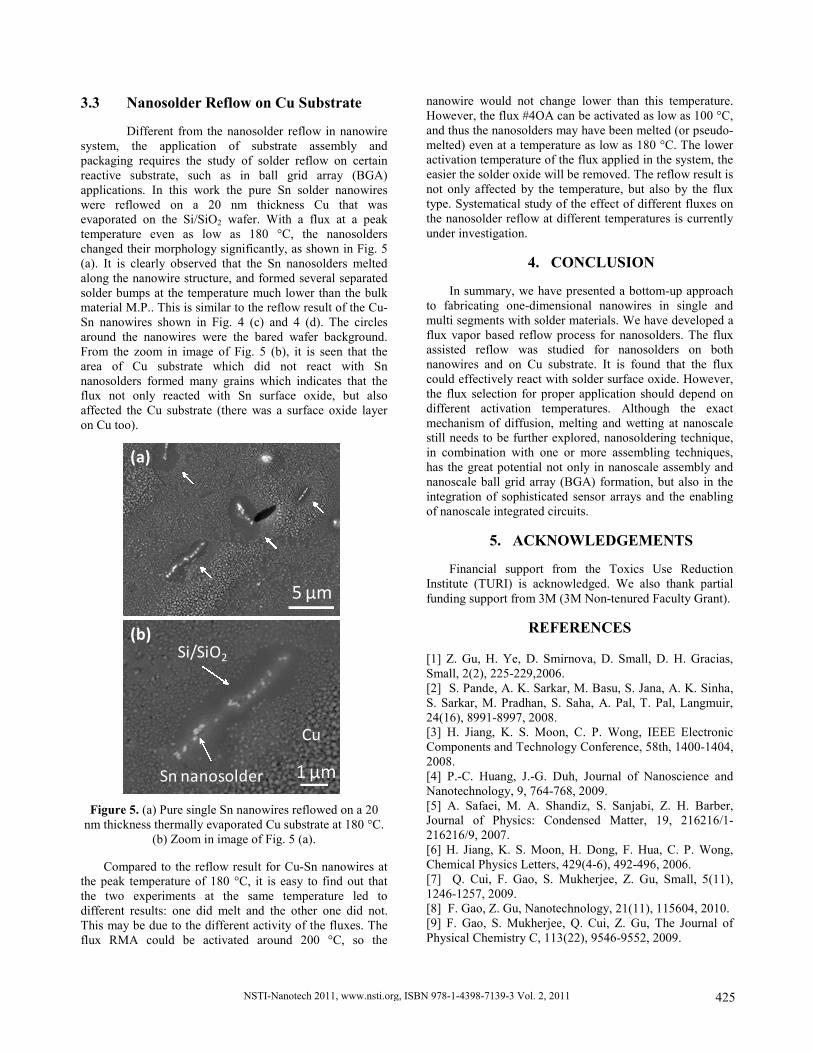
3.3 Nanosolder Reflow on Cu Substrate
Different from the nanosolder reflow in nanowiresystem, the application of substrate assembly andpackaging requires the study of solder reflow on certainreactive substrate, such as in ball grid array (BGA)applications. In this work the pure Sn solder nanowireswere reflowed on a 20 nm thickness Cu that wasevaporated on the Si/SiO2 wafer. With a flux at a peaktemperature even as low as 180 °C, the nanosolderschanged their morphology significantly, as shown in Fig. 5(a). It is clearly observed that the Sn nanosolders meltedalong the nanowire structure, and formed several separatedsolder bumps at the temperature much lower than the bulkmaterial M.P.. This is similar to the reflow result of the Cu-Sn nanowires shown in Fig. 4 (c) and 4 (d). The circlesaround the nanowires were the bared wafer background.From the zoom in image of Fig. 5 (b), it is seen that thearea of Cu substrate which did not react with Snnanosolders formed many grains which indicates that theflux not only reacted with Sn surface oxide, but alsoaffected the Cu substrate (there was a surface oxide layeron Cu too).
(a)
(b)Si/SiO2
Cu
Sn nanosolder
Figure 5. (a) Pure single Sn nanowires reflowed on a 20nm thickness thermally evaporated Cu substrate at 180 °C.
(b) Zoom in image of Fig. 5 (a).
Compared to the reflow result for Cu-Sn nanowires atthe peak temperature of 180 °C, it is easy to find out thatthe two experiments at the same temperature led todifferent results: one did melt and the other one did not.This may be due to the different activity of the fluxes. Theflux RMA could be activated around 200 °C, so the
nanowire would not change lower than this temperature.However, the flux #4OA can be activated as low as 100 °C,and thus the nanosolders may have been melted (or pseudo-melted) even at a temperature as low as 180 °C. The loweractivation temperature of the flux applied in the system, theeasier the solder oxide will be removed. The reflow result isnot only affected by the temperature, but also by the fluxtype. Systematical study of the effect of different fluxes onthe nanosolder reflow at different temperatures is currentlyunder investigation.
4. CONCLUSION
In summary, we have presented a bottom-up approachto fabricating one-dimensional nanowires in single andmulti segments with solder materials. We have developed aflux vapor based reflow process for nanosolders. The fluxassisted reflow was studied for nanosolders on bothnanowires and on Cu substrate. It is found that the fluxcould effectively react with solder surface oxide. However,the flux selection for proper application should depend ondifferent activation temperatures. Although the exactmechanism of diffusion, melting and wetting at nanoscalestill needs to be further explored, nanosoldering technique,in combination with one or more assembling techniques,has the great potential not only in nanoscale assembly andnanoscale ball grid array (BGA) formation, but also in theintegration of sophisticated sensor arrays and the enablingof nanoscale integrated circuits.
5. ACKNOWLEDGEMENTS
Financial support from the Toxics Use ReductionInstitute (TURI) is acknowledged. We also thank partialfunding support from 3M (3M Non-tenured Faculty Grant).
REFERENCES
[1] Z. Gu, H. Ye, D. Smirnova, D. Small, D. H. Gracias,Small, 2(2), 225-229,2006.[2] S. Pande, A. K. Sarkar, M. Basu, S. Jana, A. K. Sinha,S. Sarkar, M. Pradhan, S. Saha, A. Pal, T. Pal, Langmuir,24(16), 8991-8997, 2008.[3] H. Jiang, K. S. Moon, C. P. Wong, IEEE ElectronicComponents and Technology Conference, 58th, 1400-1404,2008.[4] P.-C. Huang, J.-G. Duh, Journal of Nanoscience andNanotechnology, 9, 764-768, 2009.[5] A. Safaei, M. A. Shandiz, S. Sanjabi, Z. H. Barber,Journal of Physics: Condensed Matter, 19, 216216/1-216216/9, 2007.[6] H. Jiang, K. S. Moon, H. Dong, F. Hua, C. P. Wong,Chemical Physics Letters, 429(4-6), 492-496, 2006.[7] Q. Cui, F. Gao, S. Mukherjee, Z. Gu, Small, 5(11),1246-1257, 2009.[8] F. Gao, Z. Gu, Nanotechnology, 21(11), 115604, 2010.[9] F. Gao, S. Mukherjee, Q. Cui, Z. Gu, The Journal ofPhysical Chemistry C, 113(22), 9546-9552, 2009.
NSTI-Nanotech 2011, www.nsti.org, ISBN 978-1-4398-7139-3 Vol. 2, 2011 425