datasheet.elcodis.comdatasheet.elcodis.com/pdf2/85/50/855093/dspic33fj64gs406.pdf · ¤ 2010...
TRANSCRIPT

2010 Microchip Technology Inc. Preliminary DS70591C
dsPIC33FJ32GS406/606/608/610 anddsPIC33FJ64GS406/606/608/610
Data SheetHigh-Performance,
16-bit Digital Signal Controllers
Downloaded from Elcodis.com electronic components distributor

DS70591C-page 2 Preliminary 2010 Microchip Technology Inc.
Information contained in this publication regarding deviceapplications and the like is provided only for your convenienceand may be superseded by updates. It is your responsibility toensure that your application meets with your specifications.MICROCHIP MAKES NO REPRESENTATIONS ORWARRANTIES OF ANY KIND WHETHER EXPRESS ORIMPLIED, WRITTEN OR ORAL, STATUTORY OROTHERWISE, RELATED TO THE INFORMATION,INCLUDING BUT NOT LIMITED TO ITS CONDITION,QUALITY, PERFORMANCE, MERCHANTABILITY ORFITNESS FOR PURPOSE. Microchip disclaims all liabilityarising from this information and its use. Use of Microchipdevices in life support and/or safety applications is entirely atthe buyer’s risk, and the buyer agrees to defend, indemnify andhold harmless Microchip from any and all damages, claims,suits, or expenses resulting from such use. No licenses areconveyed, implicitly or otherwise, under any Microchipintellectual property rights.
Trademarks
The Microchip name and logo, the Microchip logo, dsPIC, KEELOQ, KEELOQ logo, MPLAB, PIC, PICmicro, PICSTART, PIC32 logo, rfPIC and UNI/O are registered trademarks of Microchip Technology Incorporated in the U.S.A. and other countries.
FilterLab, Hampshire, HI-TECH C, Linear Active Thermistor, MXDEV, MXLAB, SEEVAL and The Embedded Control Solutions Company are registered trademarks of Microchip Technology Incorporated in the U.S.A.
Analog-for-the-Digital Age, Application Maestro, CodeGuard, dsPICDEM, dsPICDEM.net, dsPICworks, dsSPEAK, ECAN, ECONOMONITOR, FanSense, HI-TIDE, In-Circuit Serial Programming, ICSP, Mindi, MiWi, MPASM, MPLAB Certified logo, MPLIB, MPLINK, mTouch, Octopus, Omniscient Code Generation, PICC, PICC-18, PICDEM, PICDEM.net, PICkit, PICtail, REAL ICE, rfLAB, Select Mode, Total Endurance, TSHARC, UniWinDriver, WiperLock and ZENA are trademarks of Microchip Technology Incorporated in the U.S.A. and other countries.
SQTP is a service mark of Microchip Technology Incorporated in the U.S.A.
All other trademarks mentioned herein are property of their respective companies.
© 2010, Microchip Technology Incorporated, Printed in the U.S.A., All Rights Reserved.
Printed on recycled paper.
ISBN: 978-1-60932-027-0
Note the following details of the code protection feature on Microchip devices:
• Microchip products meet the specification contained in their particular Microchip Data Sheet.
• Microchip believes that its family of products is one of the most secure families of its kind on the market today, when used in the intended manner and under normal conditions.
• There are dishonest and possibly illegal methods used to breach the code protection feature. All of these methods, to our knowledge, require using the Microchip products in a manner outside the operating specifications contained in Microchip’s Data Sheets. Most likely, the person doing so is engaged in theft of intellectual property.
• Microchip is willing to work with the customer who is concerned about the integrity of their code.
• Neither Microchip nor any other semiconductor manufacturer can guarantee the security of their code. Code protection does not mean that we are guaranteeing the product as “unbreakable.”
Code protection is constantly evolving. We at Microchip are committed to continuously improving the code protection features of ourproducts. Attempts to break Microchip’s code protection feature may be a violation of the Digital Millennium Copyright Act. If such actsallow unauthorized access to your software or other copyrighted work, you may have a right to sue for relief under that Act.
Microchip received ISO/TS-16949:2002 certification for its worldwide headquarters, design and wafer fabrication facilities in Chandler and Tempe, Arizona; Gresham, Oregon and design centers in California and India. The Company’s quality system processes and procedures are for its PIC® MCUs and dsPIC® DSCs, KEELOQ® code hopping devices, Serial EEPROMs, microperipherals, nonvolatile memory and analog products. In addition, Microchip’s quality system for the design and manufacture of development systems is ISO 9001:2000 certified.
Downloaded from Elcodis.com electronic components distributor
2010 Microchip Technology Inc. Preliminary DS70591C-page 3
dsPIC33FJ32GS406/606/608/610 anddsPIC33FJ64GS406/606/608/610
Operating Range:
• Up to 40 MIPS operation (at 3.0-3.6V):
- Industrial temperature range (-40°C to +85°C)
- Extended temperature range (-40°C to +125°C)
High-Performance DSC CPU:
• Modified Harvard architecture
• C compiler optimized instruction set
• 16-bit wide data path
• 24-bit wide instructions
• Linear program memory addressing up to 4M instruction words
• Linear data memory addressing up to 64 Kbytes
• 83 base instructions: mostly 1 word/1 cycle
• Two 40-bit accumulators with rounding and saturation options
• Flexible and powerful addressing modes:
- Indirect
- Modulo
- Bit-Reversed
• Software stack
• 16 x 16 fractional/integer multiply operations
• 32/16 and 16/16 divide operations
• Single-cycle multiply and accumulate:
- Accumulator write back for DSP operations
- Dual data fetch
• Up to ±16-bit shifts for up to 40-bit data
Direct Memory Access (DMA):
• 4-channel hardware DMA
• 1 Kbyte dual ported DMA buffer area (DMA RAM) to store data transferred via DMA:
- Allows data transfer between RAM and a peripheral while CPU is executing code (no cycle stealing)
• Most peripherals support DMA
Digital I/O:
• Up to 85 programmable digital I/O pins
• Wake-up/Interrupt-on-Change for up to 24 pins
• Output pins can drive voltage from 3.0V to 3.6V
• Up to 5V output with open drain configuration
• 5V tolerant digital input pins
• 16 mA source/sink on all PWM pins
On-Chip Flash and SRAM:
• Flash program memory (up to 64 Kbytes)
• Data SRAM (up to 8 Kbytes)
• Boot and General Security for program Flash
Peripheral Features:
• Timer/Counters, up to five 16-bit timers
- Can pair up to make one 32-bit timer
• Input Capture (up to four channels):
- Capture on up, down or both edges
- 16-bit capture input functions
- 4-deep FIFO on each capture
• Output Compare (up to four channels):
- Single or Dual 16-bit Compare mode
- 16-bit Glitchless PWM mode
• 4-wire SPI (up to two modules):
- Framing supports I/O interface to simple codecs
- 1-deep FIFO buffer
- Supports 8-bit and 16-bit data
- Supports all serial clock formats and sampling modes
• I2C™ (up to two modules):
- Supports Full Multi-Master Slave mode
- 7-bit and 10-bit addressing
- Bus collision detection and arbitration
- Integrated signal conditioning
- Slave address masking
High-Performance, 16-Bit Digital Signal Controllers
Downloaded from Elcodis.com electronic components distributor

dsPIC33FJ32GS406/606/608/610 and dsPIC33FJ64GS406/606/608/610
DS70591C-page 4 Preliminary 2010 Microchip Technology Inc.
Peripheral Features (Continued)
• UART (up to two modules):
- Interrupt on address bit detect
- Interrupt on UART error
- Wake-up on Start bit from Sleep mode
- 4-character TX and RX FIFO buffers
- LIN bus support
- IrDA© encoding and decoding in hardware
- High-Speed Baud mode
- Hardware Flow Control with CTS and RTS
• Enhanced CAN (ECAN™ module) 2.0B active:
- Up to eight transmit and up to 32 receive buffers
- 16 receive filters and three masks
- Loopback, Listen Only and Listen All
- Messages modes for diagnostics and bus monitoring
- Wake-up on CAN message
- Automatic processing of Remote Transmission Requests
- FIFO mode using DMA
- DeviceNet™ addressing support
• Quadrature Encoder Interface (up to 2 modules):
- Phase A, Phase B, and index pulse input
- 16-bit up/down position counter
- Count direction status
- Position Measurement (x2 and x4) mode
- Programmable digital noise filters on inputs
- Alternate 16-bit Timer/Counter mode
- Interrupt on position counter rollover/underflow
High-Speed PWM Module Features:
• Up to nine PWM generators with up to 18 outputs
• Primary and Secondary time-base
• Individual time base and duty cycle for each of the PWM output
• Dead time for rising and falling edges:
- Duty cycle resolution of 1.04 ns
- Dead-time resolution of 1.04 ns
• Phase shift resolution of 1.04 ns
• Frequency resolution of 1.04 ns
• PWM modes supported:
- Standard Edge-Aligned
- True Independent Output
- Complementary
- Center-Aligned
- Push-Pull
- Multi-Phase
- Variable Phase
- Fixed Off-Time
- Current Reset
- Current-Limit
• Independent Fault/Current-Limit inputs
• Output override control
• Special Event Trigger
• PWM capture feature
• Prescaler for input clock
• Dual Trigger from PWM TO ADC
• PWMxL, PWMxH output pin swapping
• On-the-Fly PWM Frequency, Duty cycle and Phase Shift changes
• Disabling of Individual PWM generators
• Leading-Edge Blanking (LEB) functionality
High-Speed Analog Comparator:
• Up to four Analog Comparators:
- 20 ns response time
- 10-bit DAC for each analog comparator
- DACOUT pin to provide DAC output
- Programmable output polarity
- Selectable input source
- ADC sample and convert capability
• PWM module interface:
- PWM Duty Cycle Control
- PWM Period Control
- PWM Fault Detect
Interrupt Controller:
• 5-cycle latency
• Up to five external interrupts
• Seven programmable priority levels
• Five processor exceptions
High-Speed 10-bit ADC:
• 10-bit resolution
• Up to 24 input channels grouped into 12 conversion pairs
• Two internal reference monitoring inputs grouped into a pair
• Successive Approximation Register (SAR) converters for parallel conversions of analog pairs:
- 4 Msps for devices with two SARs
- 2 Msps for devices with one SAR
• Dedicated result buffer for each analog channel
• Independent trigger source section for each analog input conversion pairs
Power Management:
• On-chip 2.5V voltage regulator
• Switch between clock sources in real time
• Idle, Sleep, and Doze modes with fast wake-up
Downloaded from Elcodis.com electronic components distributor

2010 Microchip Technology Inc. Preliminary DS70591C-page 5
dsPIC33FJ32GS406/606/608/610 and dsPIC33FJ64GS406/606/608/610
CMOS Flash Technology:
• Low-power, high-speed Flash technology
• Fully static design
• 3.3V (±10%) operating voltage
• Industrial and Extended temperature
• Low power consumption
System Management:
• Flexible clock options:
- External, crystal, resonator, internal RC
- Phase-Locked Loop (PLL) with 120 MHz VCO
- Primary Crystal Oscillator (OSC) in the range of 3 MHz to 40 MHz
- Secondary oscillator (SOSC)
- Internal Low-Power RC (LPRC) oscillator at a frequency of 32.767 kHz
- Internal Fast RC (FRC) oscillator at a frequency of 7.37 MHz
• Power-on Reset (POR)
• Brown-out Reset (BOR)
• Power-up Timer (PWRT)
• Oscillator Start-up Timer (OST)
• Watchdog Timer with its RC oscillator
• Fail-Safe Clock Monitor
• Reset by multiple sources
• In-Circuit Serial Programming™ (ICSP™)
• Reference Oscillator Output
Application Examples:
• AC-to-DC Converters
• Automotive HID
• Battery Chargers
• DC-to-DC Converters
• Digital Lighting
• Induction Cooking
• LED Ballast
• Renewable Power/Pure Sine Wave Inverters
• Uninterruptible Power Supply (UPS)
Packaging:
• 64-pin QFN (9x9x0.9 mm)
• 64-pin TQFP (10x10x1 mm)
• 80-pin TQFP (12x12x1 mm)
• 100-pin TQFP (14x14x1 mm and 12x12x1 mm)
Note: See the dsPIC33FJ32GS406/606/608/610 and dsPIC33FJ64GS406/606/608/610 Controller Families table for exactperipheral features per device.
Downloaded from Elcodis.com electronic components distributor

dsPIC33FJ32GS406/606/608/610 and dsPIC33FJ64GS406/606/608/610
DS70591C-page 6 Preliminary 2010 Microchip Technology Inc.
dsPIC33FJ32GS406/606/608/610 and dsPIC33FJ64GS406/606/608/610 PRODUCT FAMILIES
The device names, pin counts, memory sizes, andperipheral availability of each device are listed inTable 1. The following pages show their pinoutdiagrams.
TABLE 1: dsPIC33FJ32GS406/606/608/610 and dsPIC33FJ64GS406/606/608/610 CONTROLLER FAMILIES
Device
Pin
s
Pro
gra
m F
las
h M
em
ory
(K
by
tes
)
RA
M (
By
tes
)
16
-bit
Tim
er
Inp
ut
Ca
ptu
re
Ou
tpu
t C
om
pa
re
UA
RT
Qu
ad
ratu
re E
nc
od
er
Inte
rfa
ce
SP
I
EC
AN
™
DM
A C
ha
nn
els
PW
M
An
alo
g C
om
pa
rato
r
Ex
tern
al
Inte
rru
pts
DA
C O
utp
ut
I2C
™
ADC
I/O
Pin
s
Pa
ck
ag
es
SA
Rs
Sa
mp
le a
nd
Ho
ld (
S&
H)
Cir
cu
it
An
alo
g-t
o-D
igit
al
Inp
uts
dsPIC33FJ32GS406 64 32 4K 5 4 4 2 1 2 0 0 6x2 0 5 0 2 1 5 16 58 PT, MR
dsPIC33FJ32GS606 64 32 4K 5 4 4 2 2 2 0 0 6x2 4 5 1 2 2 6 16 58 PT, MR
dsPIC33FJ32GS608 80 32 4K 5 4 4 2 2 2 0 0 8x2 4 5 1 2 2 6 18 74 PT
dsPIC33FJ32GS610 100 32 4K 5 4 4 2 2 2 0 0 9x2 4 5 1 2 2 6 24 85 PT, PF
dsPIC33FJ64GS406 64 64 8K 5 4 4 2 1 2 0 0 6x2 0 5 0 2 1 5 16 58 PT, MR
dsPIC33FJ64GS606 64 64 9K(1) 5 4 4 2 2 2 1 4 6x2 4 5 1 2 2 6 16 58 PT, MR
dsPIC33FJ64GS608 80 64 9K(1) 5 4 4 2 2 2 1 4 8x2 4 5 1 2 2 6 18 74 PT
dsPIC33FJ64GS610 100 64 9K(1) 5 4 4 2 2 2 1 4 9x2 4 5 1 2 2 6 24 85 PT, PF
Note 1: RAM size is inclusive of 1 Kbyte DMA RAM.
Downloaded from Elcodis.com electronic components distributor
2010 Microchip Technology Inc. Preliminary DS70591C-page 7
dsPIC33FJ32GS406/606/608/610 and dsPIC33FJ64GS406/606/608/610
Pin Diagrams
64-Pin TQFP
12345678910111213 36
353433
32
31
30
29
28
27
26
64 63 62 61 60 59 58 57 56
141516
17
18
19
20
21
22
23
24
25
dsPIC33FJ32GS406
PGEC2/SOSCO/T1CK/CN0/RC14PGED2/SOSCI/T4CK/CN1/RC13OC1/QEB1/FLT5/RD0IC4/QEA1/FLT4/INT4/RD11
IC2/FLT2/U1CTS/INT2/RD9IC1/FLT1/SYNCI1/INT1/RD8VSS
OSC2/REFCLKO/CLKO/RC15OSC1/CLKIN/RC12VDD
SCL1/RG2
U1RTS/SCK1/INT0/RF6U1RX/SDI1/RF2U1TX/SDO1/RF3
PWM3H/RE5PWM4L/RE6PWM4H/RE7
SCK2/FLT12/CN8/RG6SDI2/FLT11/CN9/RG7
SDO2/FLT10/CN10/RG8MCLR
VSS
VDD
AN3/AINDX1/CN5/RB3AN2/ASS1/CN4/RB2
PGEC3/B/AN1/CN3/RB1PGED3/AN0/CN2/RB0
PW
M5
H/U
PD
N1/
CN
16/
RD
7
PW
M3
L/R
E4
PW
M2
H/R
E3
PW
M2
L/R
E2
VC
AP/V
DD
CO
RE
PW
M1
L1/F
LT8/
RE
0
RF
1
PW
M1
H1/
RE
1
OC
2/S
YN
CO
2/F
LT6/
RD
1O
C3
/FLT
7/S
YN
CI3
/RD
2
PG
EC
1/A
N6/
OC
FA/R
B6
PG
ED
1/A
N7
/RB
7A
VD
D
AV
SS
AN
8/U
2CT
S/R
B8
AN
9/R
B9
TM
S/A
N10
/RB
10
TD
O/A
N11
/RB
11V
SS
VD
D
TC
K/A
N12
/RB
12
TD
I/A
N13
/RB
13
AN
14/
SS
1 /U
2RT
S/R
B1
4A
N15
/OC
FB
/CN
12/R
B1
5
U2T
X/S
CL2
/FLT
18/
CN
18/
RF
5
U2
RX
/SD
A2
/FLT
17/
CN
17/
RF
4
SDA1/RG3
43424140393837
44
484746
50 495154 53 5255
45
SS2/FLT9/SYNCI2/T5CK/CN11/RG9
AN5/AQEB1/CN7/RB5AN4/AQEA1/CN6/RB4
IC3/INDX1/FLT3/INT3/RD10
VD
D
SY
NC
I4/R
F0
OC
4/S
YN
CO
1/R
D3
PW
M5
L/C
N1
5/R
D6
PW
M6
H/C
N14
/RD
5P
WM
6L/
CN
13/
RD
4
dsPIC33FJ64GS406
= Pins are up to 5V tolerant
Downloaded from Elcodis.com electronic components distributor
dsPIC33FJ32GS406/606/608/610 and dsPIC33FJ64GS406/606/608/610
DS70591C-page 8 Preliminary 2010 Microchip Technology Inc.
Pin Diagrams (Continued)
64-Pin QFN
PGEC2/SOSCO/T1CK/CN0/RC14
PGED2/SOSCI/T4CK/CN1/RC13OC1/QEB1/FLT5/RD0IC4/QEA1/FLT4/INT4/RD11
IC2/FLT2/U1CTS/INT2/RD9IC1/FLT1/SYNCI1/INT1/RD8
VSS
OSC2/REFCLKO/CLKO/RC15OSC1/CLKIN/RC12
VDD
SCL1/RG2
U1RTS/SCK1/INT0/RF6U1RX/SDI1/RF2U1TX/SDO1/RF3
PWM3H/RE5PWM4L/RE6
PWM4H/RE7SCK2/FLT12/CN8/RG6SDI2/FLT11/CN9/RG7
SDO2/FLT10/CN10/RG8MCLR
VSS
VDD
AN3/AINDX1/CN5/RB3AN2/ASS1/CN4/RB2
PGEC3/B/AN1/CN3/RB1PGED3/AN0/CN2/RB0
PW
M5
H/U
PD
N1/
CN
16/R
D7
PW
M3
L/R
E4
PW
M2
H/R
E3
PW
M2
L/R
E2
VC
AP/V
DD
CO
RE
PW
M1
L1/F
LT
8/R
E0
RF
1
PW
M1
H1/
RE
1
OC
2/S
YN
CO
2/F
LT6/
RD
1O
C3
/FL
T7
/SY
NC
I3/R
D2
PG
EC
1/A
N6/
OC
FA
/RB
6
PG
ED
1/A
N7/
RB
7A
VD
D
AV
ss
AN
8/U
2CT
S/R
B8
AN
9/R
B9
TM
S/A
N1
0/R
B1
0T
DO
/AN
11/
RB
11
VS
S
VD
D
TC
K/A
N1
2/R
B1
2T
DI/
AN
13/
RB
13
AN
14/S
S1 /
U2
RT
S/R
B1
4A
N1
5/O
CF
B/C
N1
2/R
B1
5
U2
TX
/SC
L2/
FLT
18/C
N18
/RF
5U
2RX
/SD
A2/
FLT
17/C
N17
/RF
4SDA1/RG3
SS2/FLT9/SYNCI2/T5CK/CN11/RG9
AN5/AQEB1/CN7/RB5
AN4/AQEA1/CN6/RB4
IC3/INDX1/FLT3/INT3/RD10
VD
D
SY
NC
I4/R
F0
OC
4/S
YN
CO
1/R
D3
PW
M5
L/C
N1
5/R
D6
PW
M6
H/C
N14
/RD
5P
WM
6L/
CN
13/
RD
4
64 63 62 61 60 59 58 57 56 55
22 23 24 25 26 27 28 29 30 31
3
4039383736353433
45
7891011
12
4241
6
32
43
54
141516
1213
17 18 19 20 21
4544
4746
48
53 52 51 50 49
dsPIC33FJ32GS406dsPIC33FJ64GS406
= Pins are up to 5V tolerant
Note: The metal plane at the bottom of the device is not connected to any pins and is recommended to be connected toVSS externally.
Downloaded from Elcodis.com electronic components distributor

2010 Microchip Technology Inc. Preliminary DS70591C-page 9
dsPIC33FJ32GS406/606/608/610 and dsPIC33FJ64GS406/606/608/610
Pin Diagrams (Continued)
64-Pin TQFP
12345678910111213 36
353433
32
31
30
29
28
27
26
64 63 62 61 60 59 58 57 56
141516
17
18
19
20
21
22
23
24
25
PGEC2/SOSCO/T1CK/CN0/RC14PGED2/SOSCI/T4CK/CN1/RC13OC1/QEB1/FLT5/RD0IC4/QEA1/FLT4/INT4/RD11
IC2/FLT2/U1CTS/INT2/RD9IC1/FLT1/SYNCI1/INT1/RD8VSS
OSC2/REFCLKO/CLKO/RC15OSC1/CLKIN/RC12VDD
SCL1/RG2
U1RTS/SCK1/INT0/RF6U1RX/SDI1/RF2U1TX/SDO1/RF3
PWM3H/RE5PWM4L/RE6PWM4H/RE7
SCK2/FLT12/CN8/RG6SDI2/FLT11/CN9/RG7
SDO2/FLT10/CN10/RG8MCLR
VSS
VDD
AN3/CMP2B/AINDX1/CN5/RB3AN2/CMP1C/CMP2A/ASS1/CN4/RB2
PGEC3/B/AN1/CMP1B/CN3/RB1PGED3/AN0/CMP1A/CMP4C/CN2/RB0
PW
M5
H/U
PD
N1/
CN
16/R
D7
PW
M3
L/R
E4
PW
M2
H/R
E3
PW
M2
L/R
E2
VC
AP/V
DD
CO
RE
PW
M1
L1/F
LT8/
RE
0R
F1
PW
M1
H1/
RE
1
OC
2/S
YN
CO
2/F
LT6/
RD
1O
C3
/FLT
7/S
YN
CI3
/RD
2
PG
EC
1/A
N6/
CM
P3C
/CM
P4A
/OC
FA/R
B6
PG
ED
1/A
N7/
CM
P4B
/RB
7A
Vdd
AV
SS
AN
8/U
2CT
S/R
B8
AN
9/D
AC
OU
T/R
B9
TM
S/A
N10
/RB
10T
DO
/AN
11/E
XT
RE
F/R
B11
VS
S
VD
D
TC
K/A
N12
/CM
P1D
/RB
12T
DI/
AN
13/C
MP
2D/R
B13
AN
14/
CM
P3D
/SS
1 /U
2RT
S/R
B14
AN
15/C
MP
4D/O
CF
B/C
N12
/RB
15
U2
TX
/SC
L2/
FLT
18/
CN
18/
RF
5U
2R
X/S
DA
2/F
LT1
7/C
N1
7/R
F4
SDA1/RG3
43424140393837
44
484746
50 495154 53 5255
45
SS2/FLT9/SYNCI2/T5CK/CN11/RG9
AN5/CMP3B/AQEB1/CN7/RB5AN4/CMP2C/CMP3A/AQEA1/CN6/RB4
IC3/INDX1/FLT3/INT3/RD10
VD
D
SY
NC
I4/R
F0
OC
4/S
YN
CO
1/R
D3
PW
M5
L/C
N1
5/R
D6
PW
M6
H/C
N14
/RD
5P
WM
6L/
CN
13/
RD
4
dsPIC33FJ32GS606
= Pins are up to 5V tolerant
Downloaded from Elcodis.com electronic components distributor
dsPIC33FJ32GS406/606/608/610 and dsPIC33FJ64GS406/606/608/610
DS70591C-page 10 Preliminary 2010 Microchip Technology Inc.
Pin Diagrams (Continued)
64-Pin TQFP
12345678910111213 36
353433
32313029282726
64 63 62 61 60 59 58 57 56
141516
17 18 19 20 21 22 23 24 25
PGEC2/SOSCO/T1CK/CN0/RC14PGED2/SOSCI/T4CK/CN1/RC13OC1/QEB1/FLT5/RD0IC4/QEA1/FLT4/INT4/RD11
IC2/FLT2/U1CTS/INT2/RD9IC1/FLT1/SYNCI1/INT1/RD8VSS
OSC2/REFCLKO/CLKO/RC15OSC1/CLKIN/RC12VDD
SCL1/RG2
U1RTS/SCK1/INT0/RF6U1RX/SDI1/RF2U1TX/SDO1/RF3
PWM3H/RE5PWM4L/RE6PWM4H/RE7
SCK2/FLT12/CN8/RG6SDI2/FLT11/CN9/RG7
SDO2/FLT10/CN10/RG8MCLR
VSS
VDD
AN3/CMP2B/AINDX1/CN5/RB3AN2/CMP1C/CMP2A/ASS1/CN4/RB2
PGEC3/B/AN1/CMP1B/CN3/RB1PGED3/AN0/CMP1A/CMP4C/CN2/RB0
PW
M5
H/U
PD
N1/
CN
16/R
D7
PW
M3
L/R
E4
PW
M2
H/R
E3
PW
M2
L/R
E2
VC
AP/V
DD
CO
RE
PW
M1
L1/F
LT8/
RE
0C
1T
X/R
F1
PW
M1
H1/
RE
1
OC
2/S
YN
CO
2/F
LT6/
RD
1O
C3
/FLT
7/S
YN
CI3
/RD
2
PG
EC
1/A
N6/
CM
P3C
/CM
P4A
/OC
FA/R
B6
PG
ED
1/A
N7/
CM
P4B
/RB
7A
Vdd
AV
SS
AN
8/U
2C
TS
/RB
8A
N9/
DA
CO
UT
/RB
9T
MS
/AN
10/R
B10
TD
O/A
N11
/EX
TR
EF
/RB
11V
SS
VD
D
TC
K/A
N12
/CM
P1
D/R
B12
TD
I/A
N13
/CM
P2
D/R
B13
AN
14/C
MP
3D/S
S1
/U2R
TS
/RB
14A
N15
/CM
P4
D/O
CF
B/C
N12
/RB
15
U2
TX
/SC
L2/
FLT
18/
CN
18/R
F5
U2
RX
/SD
A2/
FLT
17/
CN
17/R
F4
SDA1/RG3
43424140393837
44
484746
50 495154 53 5255
45
SS2/FLT9/SYNCI2/T5CK/CN11/RG9
AN5/CMP3B/AQEB1/CN7/RB5AN4/CMP2C/CMP3A/AQEA1/CN6/RB4
IC3/INDX1/FLT3/INT3/RD10
VD
D
C1
RX
/SY
NC
I4/R
F0
OC
4/S
YN
CO
1/R
D3
PW
M5
L/C
N1
5/R
D6
PW
M6
H/C
N1
4/R
D5
PW
M6
L/C
N1
3/R
D4
dsPIC33FJ64GS606
= Pins are up to 5V tolerant
Downloaded from Elcodis.com electronic components distributor

2010 Microchip Technology Inc. Preliminary DS70591C-page 11
dsPIC33FJ32GS406/606/608/610 and dsPIC33FJ64GS406/606/608/610
Pin Diagrams (Continued)
PGEC2/SOSCO/T1CK/CN0/RC14PGED2/SOSCI/T4CK/CN1/RC13OC1/QEB1/FLT5/RD0IC4/QEA1/FLT4/INT4/RD11
IC2/FLT2/U1CTS/INT2/RD9IC1/FLT1/SYNCI1/INT1/RD8VSS
OSC2/REFCLKO/CLKO/RC15OSC1/CLKIN/RC12VDD
SCL1/RG2
U1RTS/SCK1/INT0/RF6U1RX/SDI1/RF2U1TX/SDO1/RF3
PWM3H/RE5PWM4L/RE6PWM4H/RE7
SCK2/FLT12/CN8/RG6SDI2/FLT11/CN9/RG7
SDO2/FLT10/CN10/RG8MCLR
VSS
VDD
AN3/CMP2B/AINDX1/CN5/RB3AN2/CMP1C/CMP2A/ASS1/CN4/RB2
PGEC3/B/AN1/CMP1B/CN3/RB1PGED3/AN0/CMP1A/CMP4C/CN2/RB0
PW
M5H
/UP
DN
1/C
N1
6/R
D7
PW
M3L
/RE
4P
WM
2H/R
E3
PW
M2L
/RE
2
VC
AP/V
DD
CO
RE
PW
M1L
1/F
LT8
/RE
0R
F1
PW
M1H
1/R
E1
OC
2/S
YN
CO
2/F
LT6
/RD
1O
C3/
FLT
7/S
YN
CI3
/RD
2
PG
EC
1/A
N6
/CM
P3
C/C
MP
4A/O
CF
A/R
B6
PG
ED
1/A
N7
/CM
P4
B/R
B7
AV
DD
AV
SS
AN
8/U
2CT
S/R
B8
AN
9/D
AC
OU
T/R
B9
TM
S/A
N1
0/R
B1
0T
DO
/AN
11/E
XT
RE
F/R
B11
VS
S
VD
D
TC
K/A
N1
2/C
MP
1D/R
B1
2T
DI/
AN
13/
CM
P2D
/RB
13
AN
14/C
MP
3D
/SS
1 /U
2R
TS
/RB
14
AN
15/
CM
P4D
/OC
FB
/CN
12/
RB
15
U2T
X/S
CL2
FLT
18//
CN
18/R
F5
U2R
X/S
DA
2/F
LT17
/CN
17/R
F4
SDA1/RG3
SS2/FLT9/SYNCI2/T5CK/CN11/RG9
AN5/CMP3B/AQEB1/CN7/RB5AN4/CMP2C/CMP3A/AQEA1/CN6/RB4
IC3/INDX1/FLT3/INT3/RD10
VD
D
SY
NC
I4/R
F0
OC
4/S
YN
CO
1/R
D3
PW
M5L
/CN
15/R
D6
PW
M6H
/CN
14/R
D5
PW
M6L
/CN
13/R
D4
64 63 62 61 60 59 58 57 56 55
22 23 24 25 26 27 28 29 30 31
3
4039383736353433
45
7891011
12
4241
6
32
43
54
141516
1213
17 18 19 20 21
4544
4746
48
53 52 51 50 49
dsPIC33FJ32GS606
64-Pin QFN = Pins are up to 5V tolerant
Note: The metal plane at the bottom of the device is not connected to any pins and is recommended to be connected toVSS externally.
Downloaded from Elcodis.com electronic components distributor
dsPIC33FJ32GS406/606/608/610 and dsPIC33FJ64GS406/606/608/610
DS70591C-page 12 Preliminary 2010 Microchip Technology Inc.
Pin Diagrams (Continued)
64-Pin QFN
PGEC2/SOSCO/T1CK/CN0/RC14PGED2/SOSCI/T4CK/CN1/RC13OC1/QEB1/FLT5/RD0IC4/QEA1/FLT4/INT4/RD11
IC2/FLT2/U1CTS/INT2/RD9IC1/FLT1/SYNCI1/INT1/RD8VSS
OSC2/REFCLKO/CLKO/RC15OSC1/CLKIN/RC12VDD
SCL1/RG2
U1RTS/SCK1/INT0/RF6U1RX/SDI1/RF2U1TX/SDO1/RF3
PWM3H/RE5PWM4L/RE6PWM4H/RE7
SCK2/FLT12/CN8/RG6SDI2/FLT11/CN9/RG7
SDO2/FLT10/CN10/RG8MCLR
VSS
VDD
AN3/CMP2B/AINDX1/CN5/RB3AN2/CMP1C/CMP2A/ASS1/CN4/RB2
PGEC3/B/AN1/CMP1B/CN3/RB1PGED3/AN0/CMP1A/CMP4C/CN2/RB0
PW
M5
H/U
PD
N1/
CN
16/R
D7
PW
M3
L/R
E4
PW
M2
H/R
E3
PW
M2
L/R
E2
VC
AP/V
DD
CO
RE
PW
M1
L1/F
LT8/
RE
0C
1TX
/RF
1
PW
M1
H1/
RE
1
OC
2/S
YN
CO
2/F
LT6/
RD
1O
C3
/FLT
7/S
YN
CI3
/RD
2
PG
EC
1/A
N6/
CM
P3C
/CM
P4A
/OC
FA/R
B6
PG
ED
1/A
N7/
CM
P4B
/RB
7A
VD
D
AV
SS
AN
8/U
2C
TS
/RB
8A
N9/
DA
CO
UT
/RB
9T
MS
/AN
10/R
B10
TD
O/A
N11
/EX
TR
EF
/RB
11V
SS
VD
D
TC
K/A
N12
/CM
P1
D/R
B12
TD
I/A
N13
/CM
P2
D/R
B13
AN
14/C
MP
3D/S
S1
/U2R
TS
/RB
14A
N15
/CM
P4
D/O
CF
B/C
N12
/RB
15
U2
TX
/SC
L2/
FLT
18/
CN
18/R
F5
U2
RX
/SD
A2/
FLT
17/
CN
17/R
F4
SDA1/RG3
SS2/FLT9/SYNCI2/T5CK/CN11/RG9
AN5/CMP3B/AQEB1/CN7/RB5AN4/CMP2C/CMP3A/AQEA1/CN6/RB4
IC3/INDX1/FLT3/INT3/RD10
VD
D
C1R
X/S
YN
CI4
/RF
0
OC
4/S
YN
CO
1/R
D3
PW
M5
L/C
N1
5/R
D6
PW
M6
H/C
N14
/RD
5P
WM
6L/
CN
13/
RD
4
64 63 62 61 60 59 58 57 56 55
22 23 24 25 26 27 28 29 30 31
3
4039383736353433
45
7891011
12
4241
6
32
43
54
141516
1213
17 18 19 20 21
4544
4746
48
53 52 51 50 49
dsPIC33FJ64GS606
= Pins are up to 5V tolerant
Note: The metal plane at the bottom of the device is not connected to any pins and is recommended to be connected toVSS externally.
Downloaded from Elcodis.com electronic components distributor
2010 Microchip Technology Inc. Preliminary DS70591C-page 13
dsPIC33FJ32GS406/606/608/610 and dsPIC33FJ64GS406/606/608/610
Pin Diagrams (Continued)
80-Pin TQFP
72
74
73
71
70
69
68
67
66
65
64
63
62
61
20
2
3
4
5
6
7
8
9
10
11
12
13
14
15
16
50
49
48
47
46
45
44
21
414
0
39
38
37
36
35
3423 24 25 26 27 28 29 30 31 32 33
dsPIC33FJ32GS608
17
18
19
75
1
57
56
55
54
53
52
51
60
59
58
43
42
76
78
77
79
22
80
QE
A2/
RD
12
PW
M7H
/OC
4/S
YN
CO
1/R
D3
OC
3/F
LT7
/RD
2
OC
2/S
YN
CO
2/F
LT6/
RD
1
PW
M2
L/R
E2
PW
M1
H1
/RE
1
PW
M1
L1/F
LT8
/RE
0
IND
X2
SY
NC
I4//
RG
0
QE
B2/
RG
1
RF
1
RF
0
PW
M3
L/R
E4
PW
M2
H/R
E3
PW
M5H
/UP
DN
1/C
N16
/RD
7
PW
M6
H/C
N14
/RD
5
OC1/QEB1/FLT5/RD0
IC4/QEA1/FLT4/RD11
IC2/FLT2/RD9
IC1/FLT1/SYNCI1/RD8
SDA2/INT4/FLT19/RA15
IC3/INDX1/FLT3/RD10
SCL2/INT3/FLT20/RA14VSS
OSC1/CLKIN/RC12
VDD
SCL1/RG2
U1RX/RF2
U1TX/RF3
PGEC2/SOSCO/T1CK/CN0/RC14
PGED2/SOSCI/T4CK/CN1/RC13
PW
M8
H/R
A1
0
PW
M8
L/R
A9
AV
DD
AV
SS
AN
8/U
2C
TS
/RB
8
AN
9/D
AC
OU
T/R
B9
AN
10/R
B1
0
AN
11/E
XT
RE
F/R
B11
VD
D
U2
RX
/FLT
17/
CN
17
/RF
4
U1
RT
S/F
LT16
/SY
NC
I2/C
N2
1/R
D1
5
U2
TX
/FLT
18/
CN
18
/RF
5
PG
EC
1/A
N6
CM
P3
C/C
MP
4A
//OC
FA/R
B6
PG
ED
1/A
N7
/CM
P4B
/RB
7
PWM4H/RE7
SCK2/FLT12/CN8/RG6
SDI2/FLT11/CN9/RG7
SDO2/FLT10/CN10/RG8MCLR
SS2/FLT9/T5CK/CN11/RG9
AN4/CMP2C/CMP3A/AQEA1/CN6/RB4
AN3/CMP2B/AINDX1/CN5/RB3
AN2/CMP1C/CMP2A/ASS1/CN4/RB2PGEC3/AN1/CMP1B/CN3/RB1
PGED3/AN0/CMP1A/CMP4C/CN2/RB0
VSS
VDD
PWM3H/RE5
PWM4L/RE6
TDO/FLT14/INT2/RE9
TMS/FLT13/INT1/RE8T
CK
/AN
12/C
MP
1D
/RB
12
TD
I/A
N13
/CM
P2
D/R
B1
3
AN
14
/CM
P3D
/SS
1/U
2R
TS
/RB
14
AN
15/C
MP
4D
/OC
FB
/CN
12/R
B1
5
VD
D
VC
AP/V
DD
CO
RE
PW
M6L
/CN
13/
RD
4
PW
M7L
/CN
19/
RD
13
SDA1/RG3
SDI1/RF7
SDO1/RF8
AN5/CMP3B/AQEB1/CN7/RB5
VS
SOSC2/REFCLKO/CLKO/RC15
PW
M5
L/C
N15
/RD
6
SCK1/INT0/RF6
U1
CT
S/F
LT1
5/S
YN
CI3
/CN
20
/RD
14
AN16/T2CK/RC1AN17/T3CK/RC2
= Pins are up to 5V tolerant
Downloaded from Elcodis.com electronic components distributor

dsPIC33FJ32GS406/606/608/610 and dsPIC33FJ64GS406/606/608/610
DS70591C-page 14 Preliminary 2010 Microchip Technology Inc.
Pin Diagrams (Continued)
80-Pin TQFP
72
74
73
71
70
69
68
67
66
65
64
63
62
61
20
2
3
4
5
6
7
8
9
10
11
12
13
14
15
16
50
49
48
47
46
45
44
21
41
4039383736353423
24
25
26
27
28
29
30
31
32
33
17
18
19
75
1
57
56
55
54
53
52
51
60
59
58
43
42
76
78
77
79
228
0
QE
A2
/RD
12
PW
M7
H/O
C4
/SY
NC
O1/
RD
3
OC
3/F
LT7
/RD
2
OC
2/S
YN
CO
2/F
LT6
/RD
1
PW
M2
L/R
E2
PW
M1H
1/R
E1
PW
M1
L1/
FLT
8/R
E0
IND
X2
SY
NC
I4//R
G0
QE
B2
/RG
1
C1
TX
/RF
1
C1
RX
/RF
0
PW
M3
L/R
E4
PW
M2H
/RE
3
PW
M5
H/U
PD
N1/
CN
16
/RD
7
PW
M6
H/C
N1
4/R
D5
OC1/QEB1/FLT5/RD0
IC4/QEA1/FLT4/RD11
IC2/FLT2/RD9
IC1/FLT1/SYNCI1/RD8
SDA2/INT4/FLT19/RA15
IC3/INDX1/FLT3/RD10
SCL2/INT3/FLT20/RA14VSS
OSC1/CLKIN/RC12
VDD
SCL1/RG2
U1RX/RF2
U1TX/RF3
PGEC2/SOSCO/T1CK/CN0/RC14
PGED2/SOSCI/T4CK/CN1/RC13
PW
M8H
/RA
10
PW
M8
L/R
A9
AV
DD
AV
SS
AN
8/U
2C
TS
/RB
8
AN
9/D
AC
OU
T/R
B9
AN
10
/RB
10
AN
11/E
XT
RE
F/R
B11
VD
D
U2R
X/F
LT1
7/C
N17
/RF
4
U1
RT
S/F
LT1
6/S
YN
CI2
/CN
21
/RD
15
U2
TX
/FLT
18
/CN
18/R
F5
PG
EC
1/A
N6
CM
P3
C/C
MP
4A
//O
CF
A/R
B6
PG
ED
1/A
N7
/CM
P4
B/R
B7
PWM4H/RE7
SCK2/FLT12/CN8/RG6
SDI2/FLT11/CN9/RG7
SDO2/FLT10/CN10/RG8MCLR
SS2/FLT9/T5CK/CN11/RG9
AN4/CMP2C/CMP3A/AQEA1/CN6/RB4
AN3/CMP2B/AINDX1/CN5/RB3
AN2/CMP1C/CMP2A/ASS1/CN4/RB2PGEC3/AN1/CMP1B/CN3/RB1
PGED3/AN0/CMP1A/CMP4C/CN2/RB0
VSS
VDD
PWM3H/RE5
PWM4L/RE6
TDO/FLT14/INT2/RE9
TMS/FLT13/INT1/RE8
TC
K/A
N1
2/C
MP
1D/R
B12
TD
I/AN
13
/CM
P2D
/RB
13
AN
14/C
MP
3D
/SS
1/U
2RT
S/R
B14
AN
15/
CM
P4D
/OC
FB
/CN
12
/RB
15
VD
D
VC
AP/V
DD
CO
RE
PW
M6
L/C
N1
3/R
D4
PW
M7
L/C
N1
9/R
D13
SDA1/RG3
SDI1/RF7
SDO1/RF8
AN5/CMP3B/AQEB1/CN7/RB5
VS
S
OSC2/REFCLKO/CLKO/RC15
PW
M5
L/C
N1
5/R
D6
SCK1/INT0/RF6
U1
CT
S/F
LT15
/SY
NC
I3/C
N20
/RD
14
AN16/T2CK/RC1AN17/T3CK/RC2
dsPIC33FJ64GS608
= Pins are up to 5V tolerant
Downloaded from Elcodis.com electronic components distributor

2010 Microchip Technology Inc. Preliminary DS70591C-page 15
dsPIC33FJ32GS406/606/608/610 and dsPIC33FJ64GS406/606/608/610
Pin Diagrams (Continued)
100-Pin TQFP
9294 93 91 90 89 88 87 86 85 84 83 82 81 80 79 78
20
2
3
4
5
6
7
8
9
10
11
12
13
14
15
16
65
64
63
62
61
60
59
26
56
4544434241403928 29 30 31 32 33 34 35 36 37 38
17
18
19
21
22
95
1
7677
72
71
70
69
68
67
66
75
74
73
58
57
24
23
25
9698 979927 46 47 48 49 50
55
54
53
52
51
100
PW
M6H
/CN
14/R
D5
PW
M6L
/CN
13/R
D4
PW
M7L
/CN
19/R
D13
QE
A2
/RD
12
PW
M7H
/OC
4/R
D3
OC
3/F
LT7/
RD
2O
C2/
SY
NC
O2
/FLT
6/R
D1
AN
23/C
N2
3/R
A7
AN
22/C
N2
2/R
A6
PW
M2L
/RE
2P
WM
9L
/RG
13
PW
M9H
/RG
12S
YN
CO
1/F
LT2
3/R
G1
4P
WM
1H/R
E1
PW
/M1L
/FLT
8/R
E0
IND
X2/
RG
0
PW
M3L
/RE
4P
WM
2H
/RE
3
RF
0
VC
AP/V
DD
CO
RE
PGED2/SOSCI/CN1/RC13
OC1/QEB1/FLT5/RD0
IC3/INDX1/FLT3/RD10
IC2/FLT2/RD9
IC1/FLT1/RD8
IC4/QEA1/FLT4/RD11
SDA2/FLT21/RA3
SCL2/FLT22/RA2
OSC2/REFCLKO/CLKO/RC15
OSC1/CLKIN/RC12
VDD
SCL1/RG2
SCK1/INT0/RF6
SDI1/RF7SDO1/RF8
SDA1/RG3
U1RX/RF2
U1TX/RF3
VssPGEC2/SOSCO/T1CK/CN0/RC14
PW
M8H
/RA
10P
WM
8L
/RA
9
AV
DD
AV
SS
AN
8/R
B8
AN
9/D
AC
OU
T/R
B9
AN
10/
RB
10
AN
11/E
XT
RE
F/R
B11
VD
D
U2
CT
S/R
F12
U2R
TS
/RF
13
U1C
TS
/FLT
15/
SY
NC
I3/C
N2
0/R
D14
U1R
TS
/FLT
16/
SY
NC
I2/C
N2
1/R
D15
VD
D
VS
S
PG
EC
1/A
N6
/CM
P3
C/C
MP
4A
//OC
FA/R
B6
PG
ED
1/A
N7
/CM
P4
B/R
B7
U2
TX
/FLT
18/
CN
18/R
F5
U2R
X/F
LT1
7/C
N17
/RF
4
PWM3H/RE5PWM4L/RE6PWM4H/RE7
SCK2/FLT12/CN8/RG6
VDD
TMS/RA0
AN20/FLT13/INT1/RE8AN21/FLT14/INT2/RE9
AN5/CMP3B/AQEB1/CN7/RB5AN4/CMP2C/CMP3A/AQEA1/CN6/RB4
AN3/CMP2B/AINDX1/CN5/RB3AN2/CMP1C/CMP2A/ASS1/CN4/RB2
SDI2/FLT11/CN9/RG7
SDO2/FLT10/CN10/RG8
PGEC3/AN1/CMP1B/CN3/RB1
PGED3/AN0/CMP1A/CMP4C/CN2/RB0
SYNCI1/RG15
VDD
SS2/FLT9/CN11/RG9
MCLR
AN
12/
CM
P1D
/RB
12
AN
13/
CM
P2D
/RB
13A
N1
4/C
MP
3D
/SS
1/R
B14
AN
15/
CM
P4D
/OC
FB
/CN
12/
RB
15
QE
B2/
RG
1R
F1
PW
M5H
/UP
DN
1/C
N16
/RD
7P
WM
5L
/CN
15
/RD
6
TDO/RA5
INT4/FLT19/SYNCI4/RA15
INT3/FLT20/RA14
VSS
VS
S
VSS
VD
D
TDI/RA4
TC
K/R
A1
AN16/T2CK/RC1
AN17/T3CK/RC2AN18/T4CK/RC3AN19/T5CK/RC4
dsPIC33FJ32GS610
= Pins are up to 5V tolerant
Downloaded from Elcodis.com electronic components distributor

dsPIC33FJ32GS406/606/608/610 and dsPIC33FJ64GS406/606/608/610
DS70591C-page 16 Preliminary 2010 Microchip Technology Inc.
Pin Diagrams (Continued)
92
94
93
91
90
89
88
87
86
85
84
83
82
81
80
79
78
20
2
3
4
5
6
7
8
9
10
11
12
13
14
15
16
65
64
63
62
61
60
59
26
56
4544434241403928 29 30 31 32 33 34 35 36 37 38
17
18
19
21
22
95
1
76
77
72
71
70
69
68
67
66
75
74
73
58
57
24
23
25
96
98
97
99
27 46 47 48 49 5055
54
53
52
51
100
PW
M6H
/CN
14/R
D5
PW
M6L
/CN
13/R
D4
PW
M7L
/CN
19/R
D13
QE
A2
/RD
12
PW
M7H
/OC
4/R
D3
OC
3/F
LT7
/RD
2O
C2/
SY
NC
O2/
FLT
6/R
D1
AN
23/C
N2
3/R
A7
AN
22/C
N2
2/R
A6
PW
M2L
/RE
2P
WM
9L
/RG
13
PW
M9H
/RG
12S
YN
CO
1/F
LT23
/RG
14
PW
M1H
/RE
1P
W/M
1L/F
LT8/
RE
0
IND
X2/
RG
0
PW
M3L
/RE
4P
WM
2H
/RE
3
C1R
X/R
F0
VC
AP/V
DD
CO
RE
PGED2/SOSCI/CN1/RC13
OC1/QEB1/FLT5/RD0
IC3/INDX1/FLT3/RD10
IC2/FLT2/RD9
IC1/FLT1/RD8
IC4/QEA1/FLT4/RD11
SDA2/FLT21/RA3
SCL2/FLT22/RA2
OSC2/REFCLKO/CLKO/RC15
OSC1/CLKIN/RC12
VDD
SCL1/RG2
SCK1/INT0/RF6
SDI1/RF7SDO1/RF8
SDA1/RG3
U1RX/RF2
U1TX/RF3
VssPGEC2/SOSCO/T1CK/CN0/RC14
PW
M8H
/RA
10P
WM
8L
/RA
9
AV
DD
AV
SS
AN
8/R
B8
AN
9/D
AC
OU
T/R
B9
AN
10/
RB
10A
N11
/EX
TR
EF
/RB
11
VD
D
U2C
TS
/RF
12U
2RT
S/R
F13
U1C
TS
/FLT
15/
SY
NC
I3/C
N2
0/R
D14
U1
RT
S/F
LT1
6/S
YN
CI2
/CN
21/
RD
15
VD
D
VS
S
PG
EC
1/A
N6
/CM
P3C
/CM
P4A
//O
CFA
/RB
6
PG
ED
1/A
N7
/CM
P4
B/R
B7
U2
TX
/FLT
18/
CN
18/R
F5
U2R
X/F
LT1
7/C
N17
/RF
4
PWM3H/RE5PWM4L/RE6PWM4H/RE7
SCK2/FLT12/CN8/RG6
VDD
TMS/RA0
AN20/FLT13/INT1/RE8AN21/FLT14/INT2/RE9
AN5/CMP3B/AQEB1/CN7/RB5AN4/CMP2C/CMP3A/AQEA1/CN6/RB4
AN3/CMP2B/AINDX1/CN5/RB3AN2/CMP1C/CMP2A/ASS1/CN4/RB2
SDI2/FLT11/CN9/RG7
SDO2/FLT10/CN10/RG8
PGEC3/AN1/CMP1B/CN3/RB1
PGED3/AN0/CMP1A/CMP4C/CN2/RB0
SYNCI1/RG15
VDD
SS2/FLT9/CN11/RG9
MCLRA
N1
2/C
MP
1D
/RB
12
AN
13/
CM
P2
D/R
B13
AN
14/
CM
P3
D/S
S1
/RB
14A
N1
5/C
MP
4D
/OC
FB
/CN
12/
RB
15
QE
B2/
RG
1C
1T
X/R
F1
PW
M5H
/UP
DN
1/C
N16
/RD
7P
WM
5L
/CN
15
/RD
6TDO/RA5
INT4/FLT19/SYNCI4/RA15
INT3/FLT20/RA14
VSS
VS
S
VSSV
DD
TDI/RA4
TC
K/R
A1
AN16/T2CK/RC1
AN17/T3CK/RC2AN18/T4CK/RC3AN19/T5CK/RC4
dsPIC33FJ64GS610
= Pins are up to 5V tolerant 100-Pin TQFP
Downloaded from Elcodis.com electronic components distributor

2010 Microchip Technology Inc. Preliminary DS70591C-page 17
dsPIC33FJ32GS406/606/608/610 and dsPIC33FJ64GS406/606/608/610
Table of Contents
dsPIC33FJ32GS406/606/608/610 and dsPIC33FJ64GS406/606/608/610 Product Families ............................................................... 61.0 Device Overview ........................................................................................................................................................................ 192.0 Guidelines for Getting Started with 16-bit Digital Signal Controllers .......................................................................................... 253.0 CPU............................................................................................................................................................................................ 354.0 Memory Organization ................................................................................................................................................................. 475.0 Flash Program Memory............................................................................................................................................................ 1096.0 Resets ..................................................................................................................................................................................... 1157.0 Interrupt Controller ................................................................................................................................................................... 1238.0 Direct Memory Access (DMA) .................................................................................................................................................. 1779.0 Oscillator Configuration ......................................................................................................................................................... 18710.0 Power-Saving Features............................................................................................................................................................ 19911.0 I/O Ports .................................................................................................................................................................................. 20912.0 Timer1 ...................................................................................................................................................................................... 21113.0 Timer2/3/4/5 features .............................................................................................................................................................. 21314.0 Input Capture............................................................................................................................................................................ 21915.0 Output Compare....................................................................................................................................................................... 22116.0 High-Speed PWM..................................................................................................................................................................... 22517.0 Quadrature Encoder Interface (QEI) Module ........................................................................................................................... 25518.0 Serial Peripheral Interface (SPI)............................................................................................................................................... 25919.0 Inter-Integrated Circuit (I2C™) ................................................................................................................................................. 26520.0 Universal Asynchronous Receiver Transmitter (UART) ........................................................................................................... 27321.0 Enhanced CAN (ECAN™) Module........................................................................................................................................... 27922.0 High-Speed 10-bit Analog-to-Digital Converter (ADC) ............................................................................................................. 30523.0 High-Speed Analog Comparator .............................................................................................................................................. 32924.0 Special Features ...................................................................................................................................................................... 33325.0 Instruction Set Summary .......................................................................................................................................................... 34126.0 Development Support............................................................................................................................................................... 34927.0 Electrical Characteristics .......................................................................................................................................................... 35328.0 Packaging Information.............................................................................................................................................................. 389Appendix A: Migrating from dsPIC33FJ06GS101/X02 and dsPIC33FJ16GSX02/X04 to dsPIC33FJ32GS406/606/608/610 and dsPIC33FJ64GS406/606/608/610 Devices ................................................................................................................................ 403Appendix B: Revision History............................................................................................................................................................. 404Index ................................................................................................................................................................................................. 409The Microchip Web Site ..................................................................................................................................................................... 415Customer Change Notification Service .............................................................................................................................................. 415Customer Support .............................................................................................................................................................................. 415Reader Response .............................................................................................................................................................................. 416Product Identification System ............................................................................................................................................................ 417
Downloaded from Elcodis.com electronic components distributor

dsPIC33FJ32GS406/606/608/610 and dsPIC33FJ64GS406/606/608/610
DS70591C-page 18 Preliminary 2010 Microchip Technology Inc.
TO OUR VALUED CUSTOMERS
It is our intention to provide our valued customers with the best documentation possible to ensure successful use of your Microchipproducts. To this end, we will continue to improve our publications to better suit your needs. Our publications will be refined andenhanced as new volumes and updates are introduced.
If you have any questions or comments regarding this publication, please contact the Marketing Communications Department viaE-mail at [email protected] or fax the Reader Response Form in the back of this data sheet to (480) 792-4150. Wewelcome your feedback.
Most Current Data Sheet
To obtain the most up-to-date version of this data sheet, please register at our Worldwide Web site at:
http://www.microchip.com
You can determine the version of a data sheet by examining its literature number found on the bottom outside corner of any page.The last character of the literature number is the version number, (e.g., DS30000A is version A of document DS30000).
Errata
An errata sheet, describing minor operational differences from the data sheet and recommended workarounds, may exist for currentdevices. As device/documentation issues become known to us, we will publish an errata sheet. The errata will specify the revisionof silicon and revision of document to which it applies.
To determine if an errata sheet exists for a particular device, please check with one of the following:
• Microchip’s Worldwide Web site; http://www.microchip.com• Your local Microchip sales office (see last page)When contacting a sales office, please specify which device, revision of silicon and data sheet (include literature number) you areusing.
Customer Notification System
Register on our web site at www.microchip.com to receive the most current information on all of our products.
Downloaded from Elcodis.com electronic components distributor

2010 Microchip Technology Inc. Preliminary DS70591C-page 19
dsPIC33FJ32GS406/606/608/610 and dsPIC33FJ64GS406/606/608/610
1.0 DEVICE OVERVIEW
This document contains device-specific information forthe following dsPIC33F Digital Signal Controller (DSC)devices:
• dsPIC33FJ32GS406
• dsPIC33FJ32GS606
• dsPIC33FJ32GS608
• dsPIC33FJ32GS610
• dsPIC33FJ64GS406
• dsPIC33FJ64GS606
• dsPIC33FJ64GS608
• dsPIC33FJ64GS610
The dsPIC33FJ32GS406/606/608/610 anddsPIC33FJ64GS406/606/608/610 families of devicescontain extensive Digital Signal Processor (DSP) func-tionality with a high-performance 16-bit microcontroller(MCU) architecture.
Figure 1-1 shows a general block diagram of the coreand peripheral modules in the dsPIC33FJ32GS406/606/608/610 and dsPIC33FJ64GS406/606/608/610devices. Table 1-1 lists the functions of the various pinsshown in the pinout diagrams.
Note: This data sheet summarizes the featuresof the dsPIC33FJ32GS406/606/608/610and dsPIC33FJ64GS406/606/608/610families of devices. It is not intended to bea comprehensive reference source. Tocomplement the information in this datasheet, refer to the “dsPIC33F/PIC24HFamily Reference Manual”. Please seethe Microchip web site (www.micro-chip.com) for the latest dsPIC33F/PIC24HFamily Reference Manual sections.
Downloaded from Elcodis.com electronic components distributor
dsPIC33FJ32GS406/606/608/610 and dsPIC33FJ64GS406/606/608/610
DS70591C-page 20 Preliminary 2010 Microchip Technology Inc.
FIGURE 1-1: BLOCK DIAGRAM
16
OSC1/CLKIOSC2/CLKO
VDD, VSS
TimingGeneration
MCLR
Power-upTimer
OscillatorStart-up Timer
Power-onReset
WatchdogTimer
Brown-outReset
Precision
ReferenceBand Gap
FRC/LPRCOscillators
RegulatorVoltage
VCAP/VDDCORE
IC1-4 I2C1,2
PORTA
InstructionDecode &
Control
PCH PCL
16
Program Counter
16-bit ALU
23
23
24
23
Instruction Reg
PCU
16 x 16W Register Array
ROM Latch
16
EA MUX
16
16
8
InterruptController
PSV & TableData AccessControl Block
StackControl
Logic
LoopControlLogic
Data Latch
AddressLatch
Address Latch
Program Memory
Data Latch
L
itera
l Data
16 16
16
16
Data Latch
AddressLatch
16
X RAM Y RAM
16
Y Data Bus
X Data Bus
DSP Engine
Divide Support
16
Control Signals to Various Blocks
ADC1Timers
PORTB
Address Generator Units
1-5
CNx
UART1,2PWM
9 x 2
PORTC
SPI1,2
OC1-4
AnalogComparator 1-4
Note: Not all pins or features are implemented on all device pinout configurations. See pinout diagrams for the specific pins and featurespresent on each device.
ECAN1
QEI1,2
PORTD
PORTE
PORTF
PORTG
DMA
DMA
RAM
Controller
16
16
Downloaded from Elcodis.com electronic components distributor
2010 Microchip Technology Inc. Preliminary DS70591C-page 21
dsPIC33FJ32GS406/606/608/610 and dsPIC33FJ64GS406/606/608/610
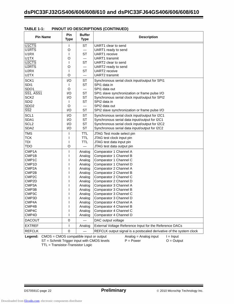
TABLE 1-1: PINOUT I/O DESCRIPTIONS
Pin NamePin
TypeBufferType
Description
AN0-AN23 I Analog Analog input channels
CLKICLKO
IO
ST/CMOS—
External clock source input. Always associated with OSC1 pin function.Oscillator crystal output. Connects to crystal or resonator in Crystal Oscillator mode. Optionally functions as CLKO in RC and EC modes. Always associated with OSC2 pin function.
OSC1
OSC2
I
I/O
ST/CMOS
—
Oscillator crystal input. ST buffer when configured in RC mode; CMOS otherwise.Oscillator crystal output. Connects to crystal or resonator in Crystal Oscillator mode. Optionally functions as CLKO in RC and EC modes.
SOSCISOSCO
IO
ST/CMOS—
32.768 kHz low-power oscillator crystal input; CMOS otherwise.32.768 kHz low-power oscillator crystal output.
CN0-CN23 I ST Change notification inputs. Can be software programmed for internal weak pull-ups on all inputs.
C1RXC1TX
IO
ST—
ECAN1 bus receive pin.ECAN1 bus transmit pin.
IC1-IC4 I ST Capture inputs 1/4
INDX1, INDX2, AINDX1QEA1, QEA2, AQEA1
QEB1, QEB2, AQEB1
UPDN1
II
I
O
STST
ST
CMOS
Quadrature Encoder Index Pulse input.Quadrature Encoder Phase A input in QEI mode. Auxiliary Timer External Clock/Gate input in Timer mode.Quadrature Encoder Phase A input in QEI mode. Auxiliary Timer External Clock/Gate input in Timer mode.Position Up/Down Counter Direction State.
OCFAOCFBOC1-OC4
IIO
STST—
Compare Fault A input (for Compare Channels 1 and 2)Compare Fault B input (for Compare Channels 3 and 4)Compare Outputs 1 through 4
INT0INT1INT2INT3INT4
IIIII
STSTSTSTST
External Interrupt 0External Interrupt 1External Interrupt 2External Interrupt 3External Interrupt 4
RA0-RA15 I/O ST PORTA is a bidirectional I/O port
RB0-RB15 I/O ST PORTB is a bidirectional I/O port
RC0-RC15 I/O ST PORTC is a bidirectional I/O port
RD0-RD15 I/O ST PORTD is a bidirectional I/O port
RE0-RE9 I/O ST PORTE is a bidirectional I/O port
RF0-RF13 I/O ST PORTF is a bidirectional I/O port
RG0-RG15 I/O ST PORTG is a bidirectional I/O port
T1CKT2CKT3CKT4CKT5CK
IIIII
STSTSTSTST
Timer1 External Clock InputTimer2 External Clock InputTimer3 External Clock InputTimer4 External Clock InputTimer5 External Clock Input
Legend: CMOS = CMOS compatible input or output Analog = Analog input I = InputST = Schmitt Trigger input with CMOS levels P = Power O = OutputTTL = Transistor-Transistor Logic
Downloaded from Elcodis.com electronic components distributor
dsPIC33FJ32GS406/606/608/610 and dsPIC33FJ64GS406/606/608/610
DS70591C-page 22 Preliminary 2010 Microchip Technology Inc.
U1CTSU1RTSU1RXU1TXU2CTSU2RTSU2RXU2TX
IOIOIOIO
ST—ST—ST—ST—
UART1 clear to sendUART1 ready to sendUART1 receiveUART1 transmitUART2 clear to sendUART2 ready to sendUART2 receiveUART2 transmit
SCK1SDI1SDO1SS1, ASS1SCK2SDI2SDO2SS2
I/OIO
I/OI/OIO
I/O
STST—STSTST—ST
Synchronous serial clock input/output for SPI1SPI1 data inSPI1 data outSPI1 slave synchronization or frame pulse I/OSynchronous serial clock input/output for SPI2SPI2 data inSPI2 data outSPI2 slave synchronization or frame pulse I/O
SCL1SDA1SCL2SDA2
I/OI/OI/OI/O
STSTSTST
Synchronous serial clock input/output for I2C1Synchronous serial data input/output for I2C1Synchronous serial clock input/output for I2C2Synchronous serial data input/output for I2C2
TMSTCKTDITDO
IIIO
TTLTTLTTL—
JTAG Test mode select pinJTAG test clock input pinJTAG test data input pinJTAG test data output pin
CMP1ACMP1BCMP1CCMP1DCMP2ACMP2BCMP2CCMP2DCMP3ACMP3BCMP3CCMP3DCMP4ACMP4BCMP4CCMP4D
IIIIIIIIIIIIIIII
AnalogAnalogAnalogAnalogAnalogAnalogAnalogAnalogAnalogAnalogAnalogAnalogAnalogAnalogAnalogAnalog
Comparator 1 Channel AComparator 1 Channel BComparator 1 Channel CComparator 1 Channel DComparator 2 Channel AComparator 2 Channel BComparator 2 Channel CComparator 2 Channel DComparator 3 Channel AComparator 3 Channel BComparator 3 Channel CComparator 3 Channel DComparator 4 Channel AComparator 4 Channel BComparator 4 Channel CComparator 4 Channel D
DACOUT 0 — DAC output voltage
EXTREF I Analog External Voltage Reference Input for the Reference DACs
REFCLK 0 — REFCLK output signal is a postscaled derivative of the system clock
TABLE 1-1: PINOUT I/O DESCRIPTIONS (CONTINUED)
Pin NamePin
TypeBufferType
Description
Legend: CMOS = CMOS compatible input or output Analog = Analog input I = InputST = Schmitt Trigger input with CMOS levels P = Power O = OutputTTL = Transistor-Transistor Logic
Downloaded from Elcodis.com electronic components distributor

2010 Microchip Technology Inc. Preliminary DS70591C-page 23
dsPIC33FJ32GS406/606/608/610 and dsPIC33FJ64GS406/606/608/610
FLT1-FLT23SYNCI1-SYNCI4SYNCO1-SYNCO2PWM1LPWM1HPWM2LPWM2HPWM3LPWM3HPWM4LPWM4HPWM5LPWM5HPWM6LPWM6HPWM7LPWM7HPWM8LPWM8HPWM9LPWM9H
IIOOOOOOOOOOOOOOOOOOO
STST———————————————————
Fault Inputs to PWM ModuleExternal synchronization signal to PWM Master Time BasePWM Master Time Base for external device synchronizationPWM1 Low outputPWM1 High outputPWM2 Low outputPWM2 High outputPWM3 Low outputPWM3 High outputPWM4 Low outputPWM4 High outputPWM5 Low outputPWM5 High outputPWM6 Low outputPWM6 High outputPWM7 Low outputPWM7 High outputPWM8 Low outputPWM8 High outputPWM9 Low outputPWM9 High output
PGED1PGEC1PGED2PGEC2PGED3PGEC3
I/OI
I/OI
I/OI
STSTSTSTSTST
Data I/O pin for programming/debugging communication Channel 1Clock input pin for programming/debugging communication Channel 1Data I/O pin for programming/debugging communication Channel 2Clock input pin for programming/debugging communication Channel 2Data I/O pin for programming/debugging communication Channel 3Clock input pin for programming/debugging communication Channel 3
MCLR I/P ST Master Clear (Reset) input. This pin is an active-low Reset to the device.
AVDD P P Positive supply for analog modules
AVSS P P Ground reference for analog modules
VDD P — Positive supply for peripheral logic and I/O pins
VCAP/VDDCORE P — CPU logic filter capacitor connection
VSS P — Ground reference for logic and I/O pins
TABLE 1-1: PINOUT I/O DESCRIPTIONS (CONTINUED)
Pin NamePin
TypeBufferType
Description
Legend: CMOS = CMOS compatible input or output Analog = Analog input I = InputST = Schmitt Trigger input with CMOS levels P = Power O = OutputTTL = Transistor-Transistor Logic
Downloaded from Elcodis.com electronic components distributor

dsPIC33FJ32GS406/606/608/610 and dsPIC33FJ64GS406/606/608/610
DS70591C-page 24 Preliminary 2010 Microchip Technology Inc.
NOTES:
Downloaded from Elcodis.com electronic components distributor

2010 Microchip Technology Inc. Preliminary DS70591C-page 25
dsPIC33FJ32GS406/606/608/610 and dsPIC33FJ64GS406/606/608/610
2.0 GUIDELINES FOR GETTING STARTED WITH 16-BIT DIGITAL SIGNAL CONTROLLERS
2.1 Basic Connection Requirements
Getting started with thedsPIC33FJ32GS406/606/608/610 anddsPIC33FJ64GS406/606/608/610 family of 16-bitDigital Signal Controllers (DSC) requires attention to aminimal set of device pin connections beforeproceeding with development. The following is a list ofpin names, which must always be connected:
• All VDD and VSS pins (see Section 2.2 “Decoupling Capacitors”)
• All AVDD and AVSS pins (regardless if ADC module is not used) (see Section 2.2 “Decoupling Capacitors”)
• VCAP/VDDCORE (see Section 2.3 “Capacitor on Internal Voltage Regulator (VCAP/VDDCORE)”)
• MCLR pin (see Section 2.4 “Master Clear (MCLR) Pin”)
• PGECx/PGEDx pins used for In-Circuit Serial Programming™ (ICSP™) and debugging purposes (see Section 2.5 “ICSP Pins”)
• OSC1 and OSC2 pins when external oscillator source is used (see Section 2.6 “External Oscillator Pins”)
2.2 Decoupling Capacitors
The use of decoupling capacitors on every pair ofpower supply pins, such as VDD, VSS, AVDD, andAVSS is required.
Consider the following criteria when using decouplingcapacitors:
• Value and type of capacitor: Recommendation of 0.1 µF (100 nF), 10-20V. This capacitor should be a low-ESR and have resonance frequency in the range of 20 MHz and higher. It is recommended that ceramic capacitors be used.
• Placement on the printed circuit board: The decoupling capacitors should be placed as close to the pins as possible. It is recommended to place the capacitors on the same side of the board as the device. If space is constricted, the capacitor can be placed on another layer on the PCB using a via; however, ensure that the trace length from the pin to the capacitor is within one-quarter inch (6 mm) in length.
• Handling high frequency noise: If the board is experiencing high frequency noise, upward of tens of MHz, add a second ceramic-type capaci-tor in parallel to the above described decoupling capacitor. The value of the second capacitor can be in the range of 0.01 µF to 0.001 µF. Place this second capacitor next to the primary decoupling capacitor. In high-speed circuit designs, consider implementing a decade pair of capacitances as close to the power and ground pins as possible. For example, 0.1 µF in parallel with 0.001 µF.
• Maximizing performance: On the board layout from the power supply circuit, run the power and return traces to the decoupling capacitors first, and then to the device pins. This ensures that the decoupling capacitors are first in the power chain. Equally important is to keep the trace length between the capacitor and the power pins to a minimum, thereby reducing PCB track inductance.
Note 1: This data sheet summarizes the featuresof the dsPIC33FJ32GS406/606/608/610and dsPIC33FJ64GS406/606/608/610family of devices. It is not intended to bea comprehensive reference source. Tocomplement the information in this datasheet, refer to the “dsPIC33F/PIC24HFamily Reference Manual”. Please seethe Microchip web site(www.microchip.com) for the latest74dsPIC33F/PIC24H Family ReferenceManual sections.
2: Some registers and associated bitsdescribed in this section may not be avail-able on all devices. Refer to Section 4.0“Memory Organization” in this datasheet for device-specific register and bitinformation.
Downloaded from Elcodis.com electronic components distributor
dsPIC33FJ32GS406/606/608/610 and dsPIC33FJ64GS406/606/608/610
DS70591C-page 26 Preliminary 2010 Microchip Technology Inc.
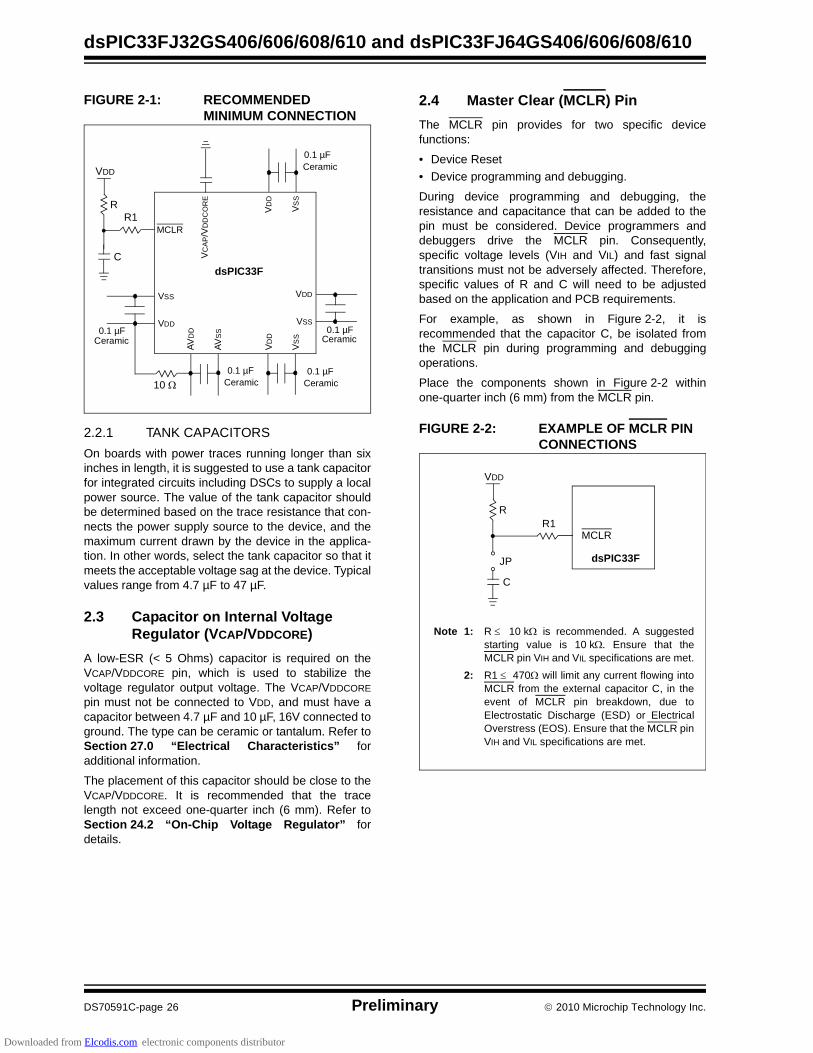
FIGURE 2-1: RECOMMENDED MINIMUM CONNECTION
2.2.1 TANK CAPACITORS
On boards with power traces running longer than sixinches in length, it is suggested to use a tank capacitorfor integrated circuits including DSCs to supply a localpower source. The value of the tank capacitor shouldbe determined based on the trace resistance that con-nects the power supply source to the device, and themaximum current drawn by the device in the applica-tion. In other words, select the tank capacitor so that itmeets the acceptable voltage sag at the device. Typicalvalues range from 4.7 µF to 47 µF.
2.3 Capacitor on Internal Voltage Regulator (VCAP/VDDCORE)
A low-ESR (< 5 Ohms) capacitor is required on theVCAP/VDDCORE pin, which is used to stabilize thevoltage regulator output voltage. The VCAP/VDDCORE
pin must not be connected to VDD, and must have acapacitor between 4.7 µF and 10 µF, 16V connected toground. The type can be ceramic or tantalum. Refer toSection 27.0 “Electrical Characteristics” foradditional information.
The placement of this capacitor should be close to theVCAP/VDDCORE. It is recommended that the tracelength not exceed one-quarter inch (6 mm). Refer toSection 24.2 “On-Chip Voltage Regulator” fordetails.
2.4 Master Clear (MCLR) Pin
The MCLR pin provides for two specific devicefunctions:
• Device Reset
• Device programming and debugging.
During device programming and debugging, theresistance and capacitance that can be added to thepin must be considered. Device programmers anddebuggers drive the MCLR pin. Consequently,specific voltage levels (VIH and VIL) and fast signaltransitions must not be adversely affected. Therefore,specific values of R and C will need to be adjustedbased on the application and PCB requirements.
For example, as shown in Figure 2-2, it isrecommended that the capacitor C, be isolated fromthe MCLR pin during programming and debuggingoperations.
Place the components shown in Figure 2-2 withinone-quarter inch (6 mm) from the MCLR pin.
FIGURE 2-2: EXAMPLE OF MCLR PIN CONNECTIONS
dsPIC33FV
DD
VS
SVDD
VSS
VSS
VDD
AV
DD
AV
SS
VD
D
VS
S
0.1 µFCeramic
0.1 µFCeramic
0.1 µFCeramic
0.1 µFCeramic
C
R
VDD
MCLR
0.1 µFCeramic
VC
AP/V
DD
CO
RE
10
R1
Note 1: R 10 k is recommended. A suggestedstarting value is 10 k. Ensure that theMCLR pin VIH and VIL specifications are met.
2: R1 470 will limit any current flowing intoMCLR from the external capacitor C, in theevent of MCLR pin breakdown, due toElectrostatic Discharge (ESD) or ElectricalOverstress (EOS). Ensure that the MCLR pinVIH and VIL specifications are met.
C
R1R
VDD
MCLR
dsPIC33FJP
Downloaded from Elcodis.com electronic components distributor
2010 Microchip Technology Inc. Preliminary DS70591C-page 27
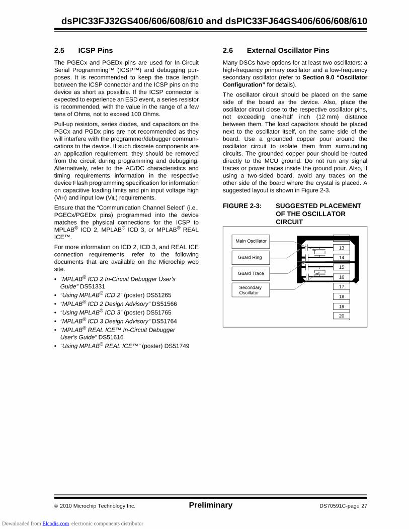
dsPIC33FJ32GS406/606/608/610 and dsPIC33FJ64GS406/606/608/610
2.5 ICSP Pins
The PGECx and PGEDx pins are used for In-CircuitSerial Programming™ (ICSP™) and debugging pur-poses. It is recommended to keep the trace lengthbetween the ICSP connector and the ICSP pins on thedevice as short as possible. If the ICSP connector isexpected to experience an ESD event, a series resistoris recommended, with the value in the range of a fewtens of Ohms, not to exceed 100 Ohms.
Pull-up resistors, series diodes, and capacitors on thePGCx and PGDx pins are not recommended as theywill interfere with the programmer/debugger communi-cations to the device. If such discrete components arean application requirement, they should be removedfrom the circuit during programming and debugging.Alternatively, refer to the AC/DC characteristics andtiming requirements information in the respectivedevice Flash programming specification for informationon capacitive loading limits and pin input voltage high(VIH) and input low (VIL) requirements.
Ensure that the “Communication Channel Select” (i.e.,PGECx/PGEDx pins) programmed into the devicematches the physical connections for the ICSP toMPLAB® ICD 2, MPLAB® ICD 3, or MPLAB® REALICE™.
For more information on ICD 2, ICD 3, and REAL ICEconnection requirements, refer to the followingdocuments that are available on the Microchip website.
• “MPLAB® ICD 2 In-Circuit Debugger User's Guide” DS51331
• “Using MPLAB® ICD 2” (poster) DS51265
• “MPLAB® ICD 2 Design Advisory” DS51566
• “Using MPLAB® ICD 3” (poster) DS51765
• “MPLAB® ICD 3 Design Advisory” DS51764
• “MPLAB® REAL ICE™ In-Circuit Debugger User's Guide” DS51616
• “Using MPLAB® REAL ICE™” (poster) DS51749
2.6 External Oscillator Pins
Many DSCs have options for at least two oscillators: ahigh-frequency primary oscillator and a low-frequencysecondary oscillator (refer to Section 9.0 “OscillatorConfiguration” for details).
The oscillator circuit should be placed on the sameside of the board as the device. Also, place theoscillator circuit close to the respective oscillator pins,not exceeding one-half inch (12 mm) distancebetween them. The load capacitors should be placednext to the oscillator itself, on the same side of theboard. Use a grounded copper pour around theoscillator circuit to isolate them from surroundingcircuits. The grounded copper pour should be routeddirectly to the MCU ground. Do not run any signaltraces or power traces inside the ground pour. Also, ifusing a two-sided board, avoid any traces on theother side of the board where the crystal is placed. Asuggested layout is shown in Figure 2-3.
FIGURE 2-3: SUGGESTED PLACEMENT OF THE OSCILLATOR CIRCUIT
13
Main Oscillator
Guard Ring
Guard Trace
SecondaryOscillator
14
15
16
17
18
19
20
Downloaded from Elcodis.com electronic components distributor

dsPIC33FJ32GS406/606/608/610 and dsPIC33FJ64GS406/606/608/610
DS70591C-page 28 Preliminary 2010 Microchip Technology Inc.
2.7 Oscillator Value Conditions on Device Start-up
If the PLL of the target device is enabled andconfigured for the device start-up oscillator, themaximum oscillator source frequency must be limitedto 4 MHz < FIN < 8 MHz to comply with device PLLstart-up conditions. This means that if the externaloscillator frequency is outside this range, theapplication must start-up in the FRC mode first. Thedefault PLL settings after a POR with an oscillatorfrequency outside this range will violate the deviceoperating speed.
Once the device powers up, the application firmwarecan initialize the PLL SFRs, CLKDIV, and PLLDBF to asuitable value, and then perform a clock switch to theOscillator + PLL clock source. Note that clock switchingmust be enabled in the device Configuration Word.
2.8 Configuration of Analog and Digital Pins During ICSP Operations
If MPLAB ICD 2, ICD 3, or REAL ICE is selected as adebugger, it automatically initializes all of the A/D inputpins (ANx) as “digital” pins, by setting all bits in theADPCFG and ADPCFG2 registers.
The bits in the registers that correspond to the A/D pinsthat are initialized by MPLAB ICD 2, ICD 3, or REALICE, must not be cleared by the user applicationfirmware; otherwise, communication errors will resultbetween the debugger and the device.
If your application needs to use certain A/D pins asanalog input pins during the debug session, the userapplication must clear the corresponding bits in theADPCFG and ADPCFG2 registers during initializationof the ADC module.
When MPLAB ICD 2, ICD 3, or REAL ICE is used as aprogrammer, the user application firmware mustcorrectly configure the ADPCFG and ADPCFG2registers. Automatic initialization of these registers isonly done during debugger operation. Failure tocorrectly configure the register(s) will result in all A/Dpins being recognized as analog input pins, resulting inthe port value being read as a logic '0', which mayaffect user application functionality.
2.9 Unused I/Os
Unused I/O pins should be configured as outputs anddriven to a logic-low state.
Alternatively, connect a 1k to 10k resistor to VSS onunused pins and drive the output to logic low.
2.10 Typical Application Connection Examples
Examples of typical application connections are shownin Figure 2-4 through Figure 2-11.
Downloaded from Elcodis.com electronic components distributor
2010 Microchip Technology Inc. Preliminary DS70591C-page 29
dsPIC33FJ32GS406/606/608/610 and dsPIC33FJ64GS406/606/608/610
FIGURE 2-4: DIGITAL PFC
FIGURE 2-5: BOOST CONVERTER IMPLEMENTATION
VAC
IPFC
VHV_BUS
ADC Channel ADC Channel ADC Channel PWM Output
|VAC|
k1
k2
k3
FET
dsPIC33FJ32GS406
Driver
IPFC
VOUTPUT
ADC Channel ADC ADC Channel PWM
k1
k2
k3
FET
dsPIC33FJ32GS406
VINPUT
Channel Output
Driver
Downloaded from Elcodis.com electronic components distributor
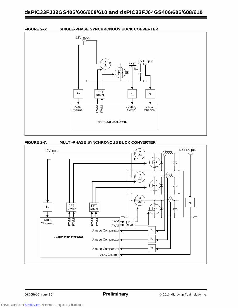
dsPIC33FJ32GS406/606/608/610 and dsPIC33FJ64GS406/606/608/610
DS70591C-page 30 Preliminary 2010 Microchip Technology Inc.
FIGURE 2-6: SINGLE-PHASE SYNCHRONOUS BUCK CONVERTER
FIGURE 2-7: MULTI-PHASE SYNCHRONOUS BUCK CONVERTER
k1
Analog Comp.
k2k7P
WM
PW
M ADC Channel
ADC Channel
5V Output
I5V
12V Input
FET Driver
dsPIC33FJ32GS606
k5
k4
k3
k6
k7
Analog Comparator
Analog Comparator
ADC Channel
Analog Comparator
ADC Channel P
WM
PW
M
PWM
PWM
PW
MP
WM
3.3V Output12V Input
FET Driver
FET Driver
FET Driver
dsPIC33FJ32GS608
Downloaded from Elcodis.com electronic components distributor
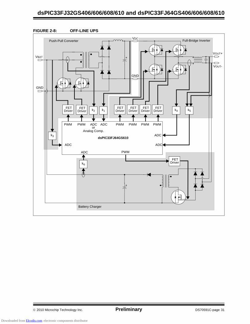
2010 Microchip Technology Inc. Preliminary DS70591C-page 31
dsPIC33FJ32GS406/606/608/610 and dsPIC33FJ64GS406/606/608/610
FIGURE 2-8: OFF-LINE UPS
ADC
ADC
ADC
ADC
ADC
PWM PWMPWM
dsPIC33FJ64GS610
PWM PWM PWM
FET Driver
FET Driver k2 k1
FET Driver
FET Driver
FET Driver
FET Driver k4 k5
VBAT
GND
+VOUT+
VOUT-
Full-Bridge InverterPush-Pull ConverterVDC
GND
FET Driver
ADC PWM
k3
k6
orAnalog Comp.
Battery Charger
+
Downloaded from Elcodis.com electronic components distributor

dsPIC33FJ32GS406/606/608/610 and dsPIC33FJ64GS406/606/608/610
DS70591C-page 32 Preliminary 2010 Microchip Technology Inc.
FIGURE 2-9: INTERLEAVED PFC
VAC
VOUT+
ADC Channel PWM ADCPWM
|VAC|
k4 k3
FET
dsPIC33FJ32GS608
Driver
VOUT-
ADC Channel
FET Driver
ADC
k1 k2
Channel Channel ADC
Channel
Downloaded from Elcodis.com electronic components distributor

2010 Microchip Technology Inc. Preliminary DS70591C-page 33
dsPIC33FJ32GS406/606/608/610 and dsPIC33FJ64GS406/606/608/610
FIGURE 2-10: PHASE-SHIFTED FULL-BRIDGE CONVERTER
VIN+
VIN-
S1
Gate 4
Gate 2
Gate 3Gate 1
AnalogGround
VOUT+
VOUT-
dsPIC33FJ32GS606
PWM
PWM ADCChannel
PWM ADCChannel
k2FET
Driver
k1
FET Driver
FET Driver
Gate 1
Gate 2
S1 Gate 3
Gate 4
S3
S3
Gate 6
Gate 5
Gat
e 6Gate 5
Downloaded from Elcodis.com electronic components distributor

ds
PIC
33
FJ
32
GS
40
6/6
06
/60
8/6
10
an
d d
sP
IC3
3F
J6
4G
S4
06
/60
6/6
08/6
10
DS
70
59
1C
-pa
ge
34
Prelim
ina
ry
20
10
Micro
chip
Te
chn
olo
gy In
c.
FIGURE 2-11: AC-TO-DC POWER SUPPLY WITH PFC AND THREE OUTPUTS (12V, 5V, AND 3.3V)
k4
ADC Channel
PWM
UART RX
PWM
PW
M
IZVT
VHV_BUS VOUTIsolation Barrier
ADC Channel
PW
M
PW
M
PW
M
FETDriver
FETDriver FET
Driver
dsPIC33FJ64GS610 k6
Analog Comp.
UART TX
k10
k7
k9
k8
k11
k5
PW
M
PW
M ADC Channel
Analog Comparator
Analog Comparator
ADC Channel
Analog Comparator
ADC Channel P
WM
PW
MPWMPWM
PW
M
PW
M
3.3V Output
5V Output
I5V
12V Input
FET Driver
FET Driver
FET Driver
FET Driver
I3.3V_3
I3.3V_2
I3.3V_1
dsPIC33FJ64GS610
VAC
IPFC
VHV_BUS
|VAC|
k1
k2
k3
FET Driver
ADCCh.
ADCCh.
PWMOutput
ADCCh.
PFC Stage
3.3V Multi-Phase Buck Stage
ZVT with Current Doubler Synchronous Rectifier
5V Buck Stage
Secondary Controller
Primary Controller
Downloaded from Elcodis.com electronic components distributor

2010 Microchip Technology Inc. Preliminary DS70591C-page 35
dsPIC33FJ32GS406/606/608/610 and dsPIC33FJ64GS406/606/608/610
3.0 CPU
The dsPIC33FJ32GS406/606/608/610 anddsPIC33FJ64GS406/606/608/610 CPU module has a16-bit (data) modified Harvard architecture with anenhanced instruction set, including significant supportfor DSP. The CPU has a 24-bit instruction word with avariable length opcode field. The Program Counter(PC) is 23 bits wide and addresses up to 4M x 24 bitsof user program memory space. The actual amount ofprogram memory implemented varies from device todevice. A single-cycle instruction prefetch mechanismis used to help maintain throughput and provides pre-dictable execution. All instructions execute in a singlecycle, with the exception of instructions that change theprogram flow, the double-word move (MOV.D)instruction and the table instructions. Overhead-freeprogram loop constructs are supported using the DOand REPEAT instructions, both of which areinterruptible at any point.
The dsPIC33FJ32GS406/606/608/610 anddsPIC33FJ64GS406/606/608/610 devices have six-teen, 16-bit working registers in the programmer’smodel. Each of the working registers can serve as adata, address or address offset register. The sixteenthworking register (W15) operates as a software StackPointer (SP) for interrupts and calls.
There are two classes of instruction in thedsPIC33FJ32GS406/606/608/610 anddsPIC33FJ64GS406/606/608/610 devices: MCU andDSP. These two instruction classes are seamlesslyintegrated into a single CPU. The instruction setincludes many addressing modes and is designed foroptimum C compiler efficiency. For most instructions,the dsPIC33FJ32GS406/606/608/610 anddsPIC33FJ64GS406/606/608/610 is capable of exe-cuting a data (or program data) memory read, a work-ing register (data) read, a data memory write and aprogram (instruction) memory read per instruction
cycle. As a result, three parameter instructions can besupported, allowing A + B = C operations to beexecuted in a single cycle.
A block diagram of the CPU is shown in Figure 3-1,and the programmer’s model for thedsPIC33FJ32GS406/606/608/610 anddsPIC33FJ64GS406/606/608/610 is shown inFigure 3-2.
3.1 Data Addressing Overview
The data space can be addressed as 32K words or64 Kbytes and is split into two blocks, referred to as Xand Y data memory. Each memory block has its ownindependent Address Generation Unit (AGU). TheMCU class of instructions operates solely throughthe X memory AGU, which accesses the entirememory map as one linear data space. Certain DSPinstructions operate through the X and Y AGUs tosupport dual operand reads, which splits the dataaddress space into two parts. The X and Y data spaceboundary is device-specific.
Overhead-free circular buffers (Modulo Addressingmode) are supported in both X and Y address spaces.The Modulo Addressing removes the softwareboundary checking overhead for DSP algorithms.Furthermore, the X AGU circular addressing can beused with any of the MCU class of instructions. The XAGU also supports Bit-Reversed Addressing to greatlysimplify input or output data reordering for radix-2 FFTalgorithms.
The upper 32 Kbytes of the data space memory mapcan optionally be mapped into program space at any16K program word boundary defined by the 8-bitProgram Space Visibility Page (PSVPAG) register. Theprogram-to-data space mapping feature lets anyinstruction access program space as if it were dataspace.
3.2 DSP Engine Overview
The DSP engine features a high-speed, 17-bit by 17-bitmultiplier, a 40-bit ALU, two 40-bit saturatingaccumulators and a 40-bit bidirectional barrel shifter.The barrel shifter is capable of shifting a 40-bit value upto 16 bits, right or left, in a single cycle. The DSPinstructions operate seamlessly with all otherinstructions and have been designed for optimal real-time performance. The MAC instruction and other asso-ciated instructions can concurrently fetch two dataoperands from memory while multiplying two Wregisters and accumulating and optionally saturatingthe result in the same cycle. This instructionfunctionality requires that the RAM data space be splitfor these instructions and linear for all others. Dataspace partitioning is achieved in a transparent andflexible manner through dedicating certain workingregisters to each address space.
Note 1: This data sheet summarizes the featuresof the dsPIC33FJ32GS406/606/608/610and dsPIC33FJ64GS406/606/608/610families of devices. It is not intended to bea comprehensive reference source. Tocomplement the information in this datasheet, refer to Section 2. “CPU”(DS70204) in the “dsPIC33F/PIC24HFamily Reference Manual”, which is avail-able from the Microchip web site(www.microchip.com).
2: Some registers and associated bitsdescribed in this section may not be avail-able on all devices. Refer to Section 4.0“Memory Organization” in this datasheet for device-specific register and bitinformation.
Downloaded from Elcodis.com electronic components distributor
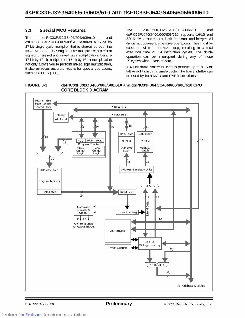
dsPIC33FJ32GS406/606/608/610 and dsPIC33FJ64GS406/606/608/610
DS70591C-page 36 Preliminary 2010 Microchip Technology Inc.
3.3 Special MCU Features
The dsPIC33FJ32GS406/606/608/610 anddsPIC33FJ64GS406/606/608/610 features a 17-bit by17-bit single-cycle multiplier that is shared by both theMCU ALU and DSP engine. The multiplier can performsigned, unsigned and mixed sign multiplication. Using a17-bit by 17-bit multiplier for 16-bit by 16-bit multiplicationnot only allows you to perform mixed sign multiplication,it also achieves accurate results for special operations,such as (-1.0) x (-1.0).
The dsPIC33FJ32GS406/606/608/610 anddsPIC33FJ64GS406/606/608/610 supports 16/16 and32/16 divide operations, both fractional and integer. Alldivide instructions are iterative operations. They must beexecuted within a REPEAT loop, resulting in a totalexecution time of 19 instruction cycles. The divideoperation can be interrupted during any of those19 cycles without loss of data.
A 40-bit barrel shifter is used to perform up to a 16-bitleft or right shift in a single cycle. The barrel shifter canbe used by both MCU and DSP instructions.
FIGURE 3-1: dsPIC33FJ32GS406/606/608/610 and dsPIC33FJ64GS406/606/608/610 CPU CORE BLOCK DIAGRAM
InstructionDecode &
Control
PCH PCLProgram Counter
16-Bit ALU
24
23
Instruction Reg
PCU
16 x 16W Register Array
ROM Latch
EA MUX
InterruptController
StackControlLogic
LoopControlLogic
Data Latch
AddressLatch
Control Signalsto Various Blocks
Lite
ral D
ata
16 16
16
To Peripheral Modules
Data Latch
AddressLatch
16
X RAM Y RAM
Address Generator Units
16
Y Data Bus
X Data Bus
DSP Engine
Divide Support
16
16
23
23
168
PSV & TableData AccessControl Block
16
16
16
16
Program Memory
Data Latch
Address Latch
Downloaded from Elcodis.com electronic components distributor

2010 Microchip Technology Inc. Preliminary DS70591C-page 37
dsPIC33FJ32GS406/606/608/610 and dsPIC33FJ64GS406/606/608/610
FIGURE 3-2: PROGRAMMER’S MODEL
PC22 PC0
7 0
D0D15
Program Counter
Data Table Page Address
STATUS Register
Working Registers
DSP OperandRegisters
W1
W2
W3
W4
W5
W6
W7
W8
W9
W10
W11
W12/DSP Offset
W13/DSP Write Back
W14/Frame Pointer
W15/Stack Pointer
DSP AddressRegisters
AD39 AD0AD31
DSPAccumulators
ACCA
ACCB
7 0
Program Space Visibility Page Address
Z
0
OA OB SA SB
RCOUNT15 0
REPEAT Loop Counter
DCOUNT15 0
DO Loop Counter
DOSTART
22 0
DO Loop Start Address
IPL2 IPL1
SPLIM Stack Pointer Limit Register
AD15
SRL
PUSH.S Shadow
DO Shadow
OAB SAB
15 0Core Configuration Register
Legend
CORCON
DA DC RA N
TBLPAG
PSVPAG
IPL0 OV
W0/WREG
SRH
DO Loop End AddressDOEND
22
C
Downloaded from Elcodis.com electronic components distributor

dsPIC33FJ32GS406/606/608/610 and dsPIC33FJ64GS406/606/608/610
DS70591C-page 38 Preliminary 2010 Microchip Technology Inc.
3.4 CPU Control Registers
REGISTER 3-1: SR: CPU STATUS REGISTER
R-0 R-0 R/C-0 R/C-0 R-0 R/C-0 R -0 R/W-0
OA OB SA(1) SB(1) OAB SAB(1,4) DA DC
bit 15 bit 8
R/W-0(2) R/W-0(3) R/W-0(3) R-0 R/W-0 R/W-0 R/W-0 R/W-0
IPL<2:0>(2) RA N OV Z C
bit 7 bit 0
Legend:
C = Clearable bit R = Readable bit U = Unimplemented bit, read as ‘0’
S = Settable bit W = Writable bit -n = Value at POR
‘1’ = Bit is set ‘0’ = Bit is cleared x = Bit is unknown
bit 15 OA: Accumulator A Overflow Status bit
1 = Accumulator A overflowed0 = Accumulator A has not overflowed
bit 14 OB: Accumulator B Overflow Status bit
1 = Accumulator B overflowed0 = Accumulator B has not overflowed
bit 13 SA: Accumulator A Saturation ‘Sticky’ Status bit(1)
1 = Accumulator A is saturated or has been saturated at some time0 = Accumulator A is not saturated
bit 12 SB: Accumulator B Saturation ‘Sticky’ Status bit(1)
1 = Accumulator B is saturated or has been saturated at some time0 = Accumulator B is not saturated
bit 11 OAB: OA || OB Combined Accumulator Overflow Status bit
1 = Accumulators A or B have overflowed0 = Neither Accumulators A or B have overflowed
bit 10 SAB: SA || SB Combined Accumulator ‘Sticky’ Status bit(1,4)
1 = Accumulators A or B are saturated or have been saturated at some time in the past0 = Neither Accumulator A or B are saturated
bit 9 DA: DO Loop Active bit
1 = DO loop in progress0 = DO loop not in progress
bit 8 DC: MCU ALU Half Carry/Borrow bit
1 = A carry-out from the 4th low-order bit (for byte-sized data) or 8th low-order bit (for word-sized data)of the result occurred
0 = No carry-out from the 4th low-order bit (for byte-sized data) or 8th low-order bit (for word-sizeddata) of the result occurred
Note 1: This bit can be read or cleared (not set).
2: The IPL<2:0> bits are concatenated with the IPL<3> bit (CORCON<3>) to form the CPU Interrupt PriorityLevel (IPL). The value in parentheses indicates the IPL if IPL<3> = 1. User interrupts are disabled whenIPL<3> = 1.
3: The IPL<2:0> Status bits are read-only when NSTDIS = 1 (INTCON1<15>).
4: Clearing this bit will clear SA and SB.
Downloaded from Elcodis.com electronic components distributor

2010 Microchip Technology Inc. Preliminary DS70591C-page 39
dsPIC33FJ32GS406/606/608/610 and dsPIC33FJ64GS406/606/608/610
bit 7-5 IPL<2:0>: CPU Interrupt Priority Level Status bits(2)
111 = CPU Interrupt Priority Level is 7 (15), user interrupts disabled110 = CPU Interrupt Priority Level is 6 (14)101 = CPU Interrupt Priority Level is 5 (13)100 = CPU Interrupt Priority Level is 4 (12)011 = CPU Interrupt Priority Level is 3 (11)010 = CPU Interrupt Priority Level is 2 (10)001 = CPU Interrupt Priority Level is 1 (9)000 = CPU Interrupt Priority Level is 0 (8)
bit 4 RA: REPEAT Loop Active bit
1 = REPEAT loop in progress0 = REPEAT loop not in progress
bit 3 N: MCU ALU Negative bit
1 = Result was negative0 = Result was non-negative (zero or positive)
bit 2 OV: MCU ALU Overflow bit
This bit is used for signed arithmetic (2’s complement). It indicates an overflow of a magnitude thatcauses the sign bit to change state. 1 = Overflow occurred for signed arithmetic (in this arithmetic operation)0 = No overflow occurred
bit 1 Z: MCU ALU Zero bit
1 = An operation that affects the Z bit has set it at some time in the past0 = The most recent operation that affects the Z bit has cleared it (i.e., a non-zero result)
bit 0 C: MCU ALU Carry/Borrow bit
1 = A carry-out from the Most Significant bit of the result occurred0 = No carry-out from the Most Significant bit of the result occurred
REGISTER 3-1: SR: CPU STATUS REGISTER (CONTINUED)
Note 1: This bit can be read or cleared (not set).
2: The IPL<2:0> bits are concatenated with the IPL<3> bit (CORCON<3>) to form the CPU Interrupt PriorityLevel (IPL). The value in parentheses indicates the IPL if IPL<3> = 1. User interrupts are disabled whenIPL<3> = 1.
3: The IPL<2:0> Status bits are read-only when NSTDIS = 1 (INTCON1<15>).
4: Clearing this bit will clear SA and SB.
Downloaded from Elcodis.com electronic components distributor
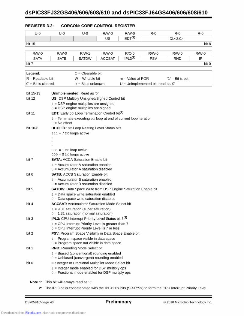
dsPIC33FJ32GS406/606/608/610 and dsPIC33FJ64GS406/606/608/610
DS70591C-page 40 Preliminary 2010 Microchip Technology Inc.
REGISTER 3-2: CORCON: CORE CONTROL REGISTER
U-0 U-0 U-0 R/W-0 R/W-0 R-0 R-0 R-0
— — — US EDT(1) DL<2:0>
bit 15 bit 8
R/W-0 R/W-0 R/W-1 R/W-0 R/C-0 R/W-0 R/W-0 R/W-0
SATA SATB SATDW ACCSAT IPL3(2) PSV RND IF
bit 7 bit 0
Legend: C = Clearable bit
R = Readable bit W = Writable bit -n = Value at POR ‘1’ = Bit is set
0’ = Bit is cleared ‘x = Bit is unknown U = Unimplemented bit, read as ‘0’
bit 15-13 Unimplemented: Read as ‘0’
bit 12 US: DSP Multiply Unsigned/Signed Control bit
1 = DSP engine multiplies are unsigned 0 = DSP engine multiplies are signed
bit 11 EDT: Early DO Loop Termination Control bit(1)
1 = Terminate executing DO loop at end of current loop iteration0 = No effect
bit 10-8 DL<2:0>: DO Loop Nesting Level Status bits
111 = 7 DO loops active•••001 = 1 DO loop active000 = 0 DO loops active
bit 7 SATA: ACCA Saturation Enable bit
1 = Accumulator A saturation enabled0 = Accumulator A saturation disabled
bit 6 SATB: ACCB Saturation Enable bit
1 = Accumulator B saturation enabled0 = Accumulator B saturation disabled
bit 5 SATDW: Data Space Write from DSP Engine Saturation Enable bit
1 = Data space write saturation enabled0 = Data space write saturation disabled
bit 4 ACCSAT: Accumulator Saturation Mode Select bit
1 = 9.31 saturation (super saturation)0 = 1.31 saturation (normal saturation)
bit 3 IPL3: CPU Interrupt Priority Level Status bit 3(2)
1 = CPU Interrupt Priority Level is greater than 70 = CPU Interrupt Priority Level is 7 or less
bit 2 PSV: Program Space Visibility in Data Space Enable bit
1 = Program space visible in data space0 = Program space not visible in data space
bit 1 RND: Rounding Mode Select bit
1 = Biased (conventional) rounding enabled0 = Unbiased (convergent) rounding enabled
bit 0 IF: Integer or Fractional Multiplier Mode Select bit
1 = Integer mode enabled for DSP multiply ops0 = Fractional mode enabled for DSP multiply ops
Note 1: This bit will always read as ‘0’.
2: The IPL3 bit is concatenated with the IPL<2:0> bits (SR<7:5>) to form the CPU Interrupt Priority Level.
Downloaded from Elcodis.com electronic components distributor

2010 Microchip Technology Inc. Preliminary DS70591C-page 41
dsPIC33FJ32GS406/606/608/610 and dsPIC33FJ64GS406/606/608/610
3.5 Arithmetic Logic Unit (ALU)
The dsPIC33FJ32GS406/606/608/610 anddsPIC33FJ64GS406/606/608/610 ALU is 16 bits wideand is capable of addition, subtraction, bit shifts and logicoperations. Unless otherwise mentioned, arithmeticoperations are 2’s complement in nature. Depending onthe operation, the ALU can affect the values of the Carry(C), Zero (Z), Negative (N), Overflow (OV) and Digit Carry(DC) Status bits in the SR register. The C and DC Statusbits operate as Borrow and Digit Borrow bits, respectively,for subtraction operations.
The ALU can perform 8-bit or 16-bit operations,depending on the mode of the instruction that is used.Data for the ALU operation can come from the Wregister array or data memory, depending on theaddressing mode of the instruction. Likewise, outputdata from the ALU can be written to the W register arrayor a data memory location.
Refer to the “16-bit MCU and DSC Programmer’s Ref-erence Manual” (DS70157) for information on the SRbits affected by each instruction.
The dsPIC33FJ32GS406/606/608/610 anddsPIC33FJ64GS406/606/608/610 CPU incorporateshardware support for both multiplication and division. Thisincludes a dedicated hardware multiplier and supporthardware for 16-bit-divisor division.
3.5.1 MULTIPLIER
Using the high-speed, 17-bit x 17-bit multiplier of theDSP engine, the ALU supports unsigned, signed ormixed sign operation in several MCU multiplicationmodes:
• 16-bit x 16-bit signed
• 16-bit x 16-bit unsigned
• 16-bit signed x 5-bit (literal) unsigned
• 16-bit unsigned x 16-bit unsigned
• 16-bit unsigned x 5-bit (literal) unsigned
• 16-bit unsigned x 16-bit signed
• 8-bit unsigned x 8-bit unsigned
3.5.2 DIVIDER
The divide block supports 32-bit/16-bit and 16-bit/16-bitsigned and unsigned integer divide operations with thefollowing data sizes:
• 32-bit signed/16-bit signed divide
• 32-bit unsigned/16-bit unsigned divide
• 16-bit signed/16-bit signed divide
• 16-bit unsigned/16-bit unsigned divide
The quotient for all divide instructions ends up in W0 andthe remainder in W1. 16-bit signed and unsigned DIVinstructions can specify any W register for both the 16-bitdivisor (Wn) and any W register (aligned) pair(W(m + 1):Wm) for the 32-bit dividend. The dividealgorithm takes one cycle per bit of divisor, so both 32-bit/16-bit and 16-bit/16-bit instructions take the samenumber of cycles to execute.
3.6 DSP Engine
The DSP engine consists of a high-speed, 17-bit x17-bit multiplier, a barrel shifter and a 40-bit adder/subtracter (with two target accumulators, round andsaturation logic).
The dsPIC33FJ32GS406/606/608/610 anddsPIC33FJ64GS406/606/608/610 is a single-cycleinstruction flow architecture; therefore, concurrent opera-tion of the DSP engine with MCU instruction flow is notpossible. However, some MCU ALU and DSP engineresources can be used concurrently by the same instruc-tion (for example, ED, EDAC).
The DSP engine can also perform inherentaccumulator-to-accumulator operations that require noadditional data. These instructions are ADD, SUB andNEG.
The DSP engine has options selected through bits inthe CPU Core Control register (CORCON), as listedbelow:
• Fractional or integer DSP multiply (IF)
• Signed or unsigned DSP multiply (US)
• Conventional or convergent rounding (RND)
• Automatic saturation on/off for ACCA (SATA)
• Automatic saturation on/off for ACCB (SATB)
• Automatic saturation on/off for writes to data memory (SATDW)
• Accumulator Saturation mode selection (ACC-SAT)
A block diagram of the DSP engine is shown inFigure 3-3.
Downloaded from Elcodis.com electronic components distributor

dsPIC33FJ32GS406/606/608/610 and dsPIC33FJ64GS406/606/608/610
DS70591C-page 42 Preliminary 2010 Microchip Technology Inc.
TABLE 3-1: DSP INSTRUCTIONS SUMMARY
FIGURE 3-3: DSP ENGINE BLOCK DIAGRAM
Instruction Algebraic Operation ACC Write Back
CLR A = 0 Yes
ED A = (x – y)2 No
EDAC A = A + (x – y)2 No
MAC A = A + (x * y) Yes
MAC A = A + x2 No
MOVSAC No change in A Yes
MPY A = x * y No
MPY A = x 2 No
MPY.N A = – x * y No
MSC A = A – x * y Yes
Zero Backfill
Sign-Extend
BarrelShifter
40-bit Accumulator A40-bit Accumulator B Round
Logic
X D
ata
Bu
s
To/From W Array
Adder
Saturate
Negate
32
3233
16
16 16
16
40 40
4040
Saturate
Y D
ata
Bu
s
40
Carry/Borrow Out
Carry/Borrow In
16
40
Multiplier/Scaler17-Bit
Downloaded from Elcodis.com electronic components distributor

2010 Microchip Technology Inc. Preliminary DS70591C-page 43
dsPIC33FJ32GS406/606/608/610 and dsPIC33FJ64GS406/606/608/610
3.6.1 MULTIPLIER
The 17-bit x 17-bit multiplier is capable of signed orunsigned operation and can multiplex its output using ascaler to support either 1.31 fractional (Q31) or 32-bitinteger results. Unsigned operands are zero-extendedinto the 17th bit of the multiplier input value. Signedoperands are sign-extended into the 17th bit of themultiplier input value. The output of the 17-bit x 17-bitmultiplier/scaler is a 33-bit value that is sign-extendedto 40 bits. Integer data is inherently represented as asigned 2’s complement value, where the MostSignificant bit (MSb) is defined as a sign bit. The rangeof an N-bit 2’s complement integer is -2N-1 to 2N-1 – 1.
• For a 16-bit integer, the data range is -32768 (0x8000) to 32767 (0x7FFF) including 0.
• For a 32-bit integer, the data range is -2,147,483,648 (0x8000 0000) to 2,147,483,647 (0x7FFF FFFF).
When the multiplier is configured for fractionalmultiplication, the data is represented as a 2’scomplement fraction, where the MSb is defined as asign bit and the radix point is implied to lie just after thesign bit (QX format). The range of an N-bit 2’scomplement fraction with this implied radix point is -1.0to (1 – 21-N). For a 16-bit fraction, the Q15 data rangeis -1.0 (0x8000) to 0.999969482 (0x7FFF) including 0and has a precision of 3.01518x10⁻⁵. In Fractionalmode, the 16 x 16 multiply operation generates a1.31 product that has a precision of 4.65661 x 10⁻¹⁰.
The same multiplier is used to support the MCUmultiply instructions, which include integer 16-bitsigned, unsigned and mixed sign multiply operations.
The MUL instruction can be directed to use byte orword-sized operands. Byte operands will direct a 16-bitresult, and word operands will direct a 32-bit result tothe specified register(s) in the W array.
3.6.2 DATA ACCUMULATORS AND ADDER/SUBTRACTER
The data accumulator consists of a 40-bit adder/subtracter with automatic sign extension logic. It canselect one of two accumulators (A or B) as its pre-accumulation source and post-accumulationdestination. For the ADD and LAC instructions, the datato be accumulated or loaded can be optionally scaledusing the barrel shifter prior to accumulation.
3.6.2.1 Adder/Subtracter, Overflow and Saturation
The adder/subtracter is a 40-bit adder with an optionalzero input into one side, and either true or complementdata into the other input.
• In the case of addition, the Carry/Borrow input is active-high and the other input is true data (not complemented).
• In the case of subtraction, the Carry/Borrow input is active-low and the other input is complemented.
The adder/subtracter generates Overflow Status bits,SA/SB and OA/OB, which are latched and reflected inthe STATUS register:
• Overflow from bit 39: this is a catastrophic overflow in which the sign of the accumulator is destroyed.
• Overflow into guard bits, 32 through 39: this is a recoverable overflow. This bit is set whenever all the guard bits are not identical to each other.
The adder has an additional saturation block thatcontrols accumulator data saturation, if selected. Ituses the result of the adder, the Overflow Status bitsdescribed previously and the SAT<A:B>(CORCON<7:6>) and ACCSAT (CORCON<4>) modecontrol bits to determine when and to what value tosaturate.
Six STATUS register bits support saturation andoverflow:
• OA: ACCA overflowed into guard bits
• OB: ACCB overflowed into guard bits
• SA: ACCA saturated (bit 31 overflow and saturation)orACCA overflowed into guard bits and saturated (bit 39 overflow and saturation)
• SB: ACCB saturated (bit 31 overflow and saturation)orACCB overflowed into guard bits and saturated (bit 39 overflow and saturation)
• OAB: Logical OR of OA and OB
• SAB: Logical OR of SA and SB
The OA and OB bits are modified each time datapasses through the adder/subtracter. When set, theyindicate that the most recent operation has overflowedinto the accumulator guard bits (bits 32 through 39).The OA and OB bits can also optionally generate anarithmetic warning trap when set and the correspond-ing Overflow Trap Flag Enable bits (OVATE, OVBTE)in the INTCON1 register are set (refer to Section 7.0“Interrupt Controller”). This allows the user applica-tion to take immediate action, for example, to correctsystem gain.
Downloaded from Elcodis.com electronic components distributor
dsPIC33FJ32GS406/606/608/610 and dsPIC33FJ64GS406/606/608/610
DS70591C-page 44 Preliminary 2010 Microchip Technology Inc.
The SA and SB bits are modified each time datapasses through the adder/subtracter, but can only becleared by the user application. When set, they indicatethat the accumulator has overflowed its maximumrange (bit 31 for 32-bit saturation or bit 39 for 40-bitsaturation) and will be saturated (if saturation isenabled). When saturation is not enabled, SA and SBdefault to bit 39 overflow and thus, indicate that a cata-strophic overflow has occurred. If the COVTE bit in theINTCON1 register is set, SA and SB bits will generatean arithmetic warning trap when saturation is disabled.
The Overflow and Saturation Status bits can optionallybe viewed in the STATUS Register (SR) as the logicalOR of OA and OB (in bit OAB) and the logical OR of SAand SB (in bit SAB). Programmers can check one bit inthe STATUS register to determine if either accumulatorhas overflowed, or one bit to determine if eitheraccumulator has saturated. This is useful for complexnumber arithmetic, which typically uses bothaccumulators.
The device supports three Saturation and Overflowmodes:
• Bit 39 Overflow and Saturation:When bit 39 overflow and saturation occurs, the saturation logic loads the maximally positive 9.31 (0x7FFFFFFFFF) or maximally negative 9.31 value (0x8000000000) into the target accumu-lator. The SA or SB bit is set and remains set until cleared by the user application. This condition is referred to as ‘super saturation’ and provides protection against erroneous data or unexpected algorithm problems (such as gain calculations).
• Bit 31 Overflow and Saturation:When bit 31 overflow and saturation occurs, the saturation logic then loads the maximally positive 1.31 value (0x007FFFFFFF) or maximally nega-tive 1.31 value (0x0080000000) into the target accumulator. The SA or SB bit is set and remains set until cleared by the user application. When this Saturation mode is in effect, the guard bits are not used, so the OA, OB or OAB bits are never set.
• Bit 39 Catastrophic Overflow:The bit 39 Overflow Status bit from the adder is used to set the SA or SB bit, which remains set until cleared by the user application. No saturation operation is performed, and the accumulator is allowed to overflow, destroying its sign. If the COVTE bit in the INTCON1 register is set, a catastrophic overflow can initiate a trap exception.
3.6.3 ACCUMULATOR ‘WRITE BACK’
The MAC class of instructions (with the exception ofMPY, MPY.N, ED and EDAC) can optionally write arounded version of the high word (bits 31 through 16)of the accumulator that is not targeted by the instructioninto data space memory. The write is performed acrossthe X bus into combined X and Y address space. Thefollowing addressing modes are supported:
• W13, Register Direct:The rounded contents of the non-target accumulator are written into W13 as a 1.15 fraction.
• [W13] + = 2, Register Indirect with Post-Increment:The rounded contents of the non-target accumulator are written into the address pointed to by W13 as a 1.15 fraction. W13 is then incremented by 2 (for a word write).
3.6.3.1 Round Logic
The round logic is a combinational block that performsa conventional (biased) or convergent (unbiased)round function during an accumulator write (store). TheRound mode is determined by the state of the RND bitin the CORCON register. It generates a 16-bit,1.15 data value that is passed to the data space writesaturation logic. If rounding is not indicated by theinstruction, a truncated 1.15 data value is stored andthe least significant word is simply discarded.
Conventional rounding zero-extends bit 15 of the accu-mulator and adds it to the ACCxH word (bits 16 through31 of the accumulator).
• If the ACCxL word (bits 0 through 15 of the accumulator) is between 0x8000 and 0xFFFF (0x8000 included), ACCxH is incremented.
• If ACCxL is between 0x0000 and 0x7FFF, ACCxH is left unchanged.
A consequence of this algorithm is that over asuccession of random rounding operations, the valuetends to be biased slightly positive.
Convergent (or unbiased) rounding operates in thesame manner as conventional rounding, except whenACCxL equals 0x8000. In this case, the LeastSignificant bit (bit 16 of the accumulator) of ACCxH isexamined:
• If it is ‘1’, ACCxH is incremented.• If it is ‘0’, ACCxH is not modified.
Assuming that bit 16 is effectively random in nature,this scheme removes any rounding bias that mayaccumulate.
The SAC and SAC.R instructions store either atruncated (SAC), or rounded (SAC.R) version of thecontents of the target accumulator to data memory viathe X bus, subject to data saturation (seeSection 3.6.3.2 “Data Space Write Saturation”). Forthe MAC class of instructions, the accumulator write-back operation functions in the same manner,addressing combined MCU (X and Y) data spacethough the X bus. For this class of instructions, the datais always subject to rounding.
Downloaded from Elcodis.com electronic components distributor

2010 Microchip Technology Inc. Preliminary DS70591C-page 45
dsPIC33FJ32GS406/606/608/610 and dsPIC33FJ64GS406/606/608/610
3.6.3.2 Data Space Write Saturation
In addition to adder/subtracter saturation, writes to dataspace can also be saturated, but without affecting thecontents of the source accumulator. The data spacewrite saturation logic block accepts a 16-bit, 1.15fractional value from the round logic block as its input,together with overflow status from the original source(accumulator) and the 16-bit round adder. These inputsare combined and used to select the appropriate1.15 fractional value as output to write to data spacememory.
If the SATDW bit in the CORCON register is set, data(after rounding or truncation) is tested for overflow andadjusted accordingly:
• For input data greater than 0x007FFF, data written to memory is forced to the maximum positive 1.15 value, 0x7FFF.
• For input data less than 0xFF8000, data written to memory is forced to the maximum negative 1.15 value, 0x8000.
The Most Significant bit of the source (bit 39) is used todetermine the sign of the operand being tested.
If the SATDW bit in the CORCON register is not set, theinput data is always passed through unmodified underall conditions.
3.6.4 BARREL SHIFTER
The barrel shifter can perform up to 16-bit arithmetic orlogic right shifts, or up to 16-bit left shifts in a singlecycle. The source can be either of the two DSPaccumulators or the X bus (to support multi-bit shifts ofregister or memory data).
The shifter requires a signed binary value to determineboth the magnitude (number of bits) and direction of theshift operation. A positive value shifts the operand right.A negative value shifts the operand left. A value of ‘0’does not modify the operand.
The barrel shifter is 40 bits wide, thereby obtaining a40-bit result for DSP shift operations and a 16-bit resultfor MCU shift operations. Data from the X bus ispresented to the barrel shifter between bit positions 16and 31 for right shifts, and between bit positions 0 and16 for left shifts.
Downloaded from Elcodis.com electronic components distributor

dsPIC33FJ32GS406/606/608/610 and dsPIC33FJ64GS406/606/608/610
DS70591C-page 46 Preliminary 2010 Microchip Technology Inc.
NOTES:
Downloaded from Elcodis.com electronic components distributor
2010 Microchip Technology Inc. Preliminary DS70591C-page 47
dsPIC33FJ32GS406/606/608/610 and dsPIC33FJ64GS406/606/608/610
4.0 MEMORY ORGANIZATION
The dsPIC33FJ32GS406/606/608/610 anddsPIC33FJ64GS406/606/608/610 architecture featuresseparate program and data memory spaces and buses.This architecture also allows the direct access to programmemory from the data space during code execution.
4.1 Program Address Space
The program address memory space of thedsPIC33FJ32GS406/606/608/610 anddsPIC33FJ64GS406/606/608/610 devices is 4Minstructions. The space is addressable by a 24-bitvalue derived either from the 23-bit Program Counter(PC) during program execution, or from table operationor data space remapping as described in Section 4.6“Interfacing Program and Data Memory Spaces”.
User application access to the program memory spaceis restricted to the lower half of the address range(0x000000 to 0x7FFFFF). The exception is the use ofTBLRD/TBLWT operations, which use TBLPAG<7> topermit access to the Configuration bits and Device IDsections of the configuration memory space.
The memory maps for thedsPIC33FJ32GS406/606/608/610 anddsPIC33FJ64GS406/606/608/610 devices are shownin Figure 4-1.
FIGURE 4-1: PROGRAM MEMORY MAPS FOR dsPIC33FJ32GS406/606/608/610 and dsPIC33FJ64GS406/606/608/610 DEVICES
Note: This data sheet summarizes the featuresof the dsPIC33FJ32GS406/606/608/610and dsPIC33FJ64GS406/606/608/610families of devices. It is not intended to bea comprehensive reference source. Tocomplement the information in this datasheet, refer to the dsPIC33F/PIC24HFamily Reference Manual, “Section 4.Program Memory” (DS70202), which isavailable from the Microchip web site(www.microchip.com).
Reset Address
0x000000
0x0000FE
0x000002
0x000100
Device Configuration
User ProgramFlash Memory
0x0058000x0057FE
(11008 instructions)
0x800000
0xF80000Registers 0xF80017
0xF80018
DEVID (2)0xFEFFFE0xFF0000
0xFFFFFE
0xF7FFFE
Unimplemented
(Read ‘0’s)
GOTO Instruction
0x000004
Reserved
0x7FFFFE
Reserved
0x0002000x0001FE0x000104
Alternate Vector Table
Reserved
Interrupt Vector Table
dsPIC33FJ32GS406/606/608/610
Co
nfig
ura
tion
Me
mo
ry S
pace
Use
r M
em
ory
Spa
ce
Reset Address
0x000000
0x0000FE
0x000002
0x000100
Device Configuration
User ProgramFlash Memory
0x00AC000x00ABFE
(21760 instructions)
0x800000
0xF80000Registers 0xF80017
0xF80018
0xF7FFFE
Unimplemented
(Read ‘0’s)
GOTO Instruction
0x000004
Reserved
0x7FFFFE
Reserved
0x0002000x0001FE0x000104
Alternate Vector Table
Reserved
Interrupt Vector Table
dsPIC33FJ64GS406/606/608/610
Co
nfig
ura
tion
Me
mo
ry S
pace
Use
r M
em
ory
Spa
ce
Reserved0xFF0002
DEVID (2)
Reserved
0xFEFFFE
0xFF0000
0xFFFFFE0xFF0002
Downloaded from Elcodis.com electronic components distributor
dsPIC33FJ32GS406/606/608/610 and dsPIC33FJ64GS406/606/608/610
DS70591C-page 48 Preliminary 2010 Microchip Technology Inc.
4.1.1 PROGRAM MEMORY ORGANIZATION
The program memory space is organized inword-addressable blocks. Although it is treated as24 bits wide, it is more appropriate to think of eachaddress of the program memory as a lower and upperword, with the upper byte of the upper word beingunimplemented. The lower word always has an evenaddress, while the upper word has an odd address (seeFigure 4-2).
Program memory addresses are always word-alignedon the lower word, and addresses are incremented ordecremented by two during the code execution. Thisarrangement provides compatibility with data memoryspace addressing and makes data in the programmemory space accessible.
4.1.2 INTERRUPT AND TRAP VECTORS
All dsPIC33FJ32GS406/606/608/610 anddsPIC33FJ64GS406/606/608/610 devices reserve theaddresses between 0x00000 and 0x000200 forhard-coded program execution vectors. A hardwareReset vector is provided to redirect code execution fromthe default value of the PC on device Reset to the actualstart of code. A GOTO instruction is programmed by theuser application at 0x000000, with the actual address forthe start of code at 0x000002.
The dsPIC33FJ32GS406/606/608/610 anddsPIC33FJ64GS406/606/608/610 devices also havetwo interrupt vector tables, located from 0x000004 to0x0000FF and 0x000100 to 0x0001FF. These vectortables allow each of the device interrupt sources to behandled by separate Interrupt Service Routines (ISRs).A more detailed discussion of the interrupt vectortables is provided in Section 7.1 “Interrupt VectorTable”.
FIGURE 4-2: PROGRAM MEMORY ORGANIZATION
0816
PC Address
0x000000
0x000002
0x0000040x000006
230000000000000000
00000000
00000000
Program Memory‘Phantom’ Byte
(read as ‘0’)
least significant wordmost significant word
Instruction Width
0x000001
0x000003
0x0000050x000007
mswAddress (lsw Address)
Downloaded from Elcodis.com electronic components distributor

2010 Microchip Technology Inc. Preliminary DS70591C-page 49
dsPIC33FJ32GS406/606/608/610 and dsPIC33FJ64GS406/606/608/610
4.2 Data Address Space
The dsPIC33FJ32GS406/606/608/610 anddsPIC33FJ64GS406/606/608/610 CPU has a separate16-bit-wide data memory space. The data space isaccessed using separate Address Generation Units(AGUs) for read and write operations. The data memorymaps is shown in Figure 4-3.
All Effective Addresses (EAs) in the data memory spaceare 16 bits wide and point to bytes within the data space.This arrangement gives a data space address range of64 Kbytes or 32K words. The lower half of the datamemory space (that is, when EA<15> = 0) is used forimplemented memory addresses, while the upper half(EA<15> = 1) is reserved for the Program SpaceVisibility area (see Section 4.6.3 “Reading Data FromProgram Memory Using Program Space Visibility”).
The dsPIC33FJ32GS406/606/608/610 anddsPIC33FJ64GS406/606/608/610 devices implementup to 9 Kbytes of data memory. Should an EA point toa location outside of this area, an all-zero word or bytewill be returned.
4.2.1 DATA SPACE WIDTH
The data memory space is organized in byteaddressable, 16-bit wide blocks. Data is aligned in datamemory and registers as 16-bit words, but all dataspace EAs resolve to bytes. The Least SignificantBytes (LSBs) of each word have even addresses, whilethe Most Significant Bytes (MSBs) have oddaddresses.
4.2.2 DATA MEMORY ORGANIZATION AND ALIGNMENT
To maintain backward compatibility with PIC® MCUdevices and improve data space memory usageefficiency, the dsPIC33FJ32GS406/606/608/610 anddsPIC33FJ64GS406/606/608/610 instruction set sup-ports both word and byte operations. As a conse-quence of byte accessibility, all effective addresscalculations are internally scaled to step throughword-aligned memory. For example, the core recog-nizes that Post-Modified Register Indirect Addressingmode [Ws++] that results in a value of Ws + 1 for byteoperations and Ws + 2 for word operations.
Data byte reads will read the complete word thatcontains the byte, using the LSB of any EA todetermine which byte to select. The selected byte isplaced onto the LSB of the data path. That is, datamemory and registers are organized as two parallelbyte-wide entities with shared (word) address decodebut separate write lines. Data byte writes only write tothe corresponding side of the array or register thatmatches the byte address.
All word accesses must be aligned to an even address.Misaligned word data fetches are not supported, socare must be taken when mixing byte and wordoperations, or translating from 8-bit MCU code. If amisaligned read or write is attempted, an address errortrap is generated. If the error occurred on a read, theinstruction underway is completed. If the error occurredon a write, the instruction is executed but the write doesnot occur. In either case, a trap is then executed,allowing the system and/or user application to examinethe machine state prior to execution of the addressFault.
All byte loads into any W register are loaded into theLeast Significant Byte. The Most Significant Byte is notmodified.
A sign-extend instruction (SE) is provided to allow userapplications to translate 8-bit signed data to 16-bitsigned values. Alternatively, for 16-bit unsigned data,user applications can clear the MSB of any W registerby executing a zero-extend (ZE) instruction on theappropriate address.
4.2.3 SFR SPACE
The first 2 Kbytes of the Near Data Space, from 0x0000to 0x07FF, is primarily occupied by Special FunctionRegisters (SFRs). These are used by thedsPIC33FJ32GS406/606/608/610 anddsPIC33FJ64GS406/606/608/610 core and peripheralmodules for controlling the operation of the device.
SFRs are distributed among the modules that theycontrol, and are generally grouped together by module.Much of the SFR space contains unused addresses;these are read as ‘0’.
4.2.4 NEAR DATA SPACE
The 8 Kbyte area between 0x0000 and 0x1FFF isreferred to as the near data space. Locations in thisspace are directly addressable via a 13-bit absoluteaddress field within all memory direct instructions.Additionally, the whole data space is addressable usingMOV instructions, which support Memory DirectAddressing mode with a 16-bit address field, or byusing Indirect Addressing mode using a workingregister as an Address Pointer.
Note: The actual set of peripheral features andinterrupts varies by the device. Refer tothe corresponding device tables andpinout diagrams for device-specific information.
Downloaded from Elcodis.com electronic components distributor

dsPIC33FJ32GS406/606/608/610 and dsPIC33FJ64GS406/606/608/610
DS70591C-page 50 Preliminary 2010 Microchip Technology Inc.
FIGURE 4-3: DATA MEMORY MAP FOR DEVICES WITH 4 KB RAM
0x0000
0x07FE
0x17FE
0xFFFE
LSBAddress16 bits
LSbMSb
MSBAddress
0x0001
0x07FF
0xFFFF
OptionallyMappedinto ProgramMemory
0x0801 0x0800
0x1800
2 KbyteSFR Space
0x8001 0x8000
SFR Space
X DataUnimplemented (X)
0x0FFE0x1000
0x0FFF0x1001
0x17FF0x1801
6 KbyteNear Data
Space
X Data RAM (X)
Y Data RAM (Y)
Downloaded from Elcodis.com electronic components distributor

2010 Microchip Technology Inc. Preliminary DS70591C-page 51
dsPIC33FJ32GS406/606/608/610 and dsPIC33FJ64GS406/606/608/610
FIGURE 4-4: DATA MEMORY MAP FOR DEVICES WITH 8 KB RAM
0x0000
0x07FE
0x27FE
0xFFFE
LSBAddress16 bits
LSbMSb
MSBAddress
0x0001
0x07FF
0xFFFF
OptionallyMappedinto ProgramMemory
0x0801 0x0800
0x2800
2 KbyteSFR Space
0x8001 0x8000
SFR Space
X DataUnimplemented (X)
0x17FE0x1800
0x17FF0x1801
0x27FF0x2801
0x1FFF 0x1FFE
0x2001 0x2000
8 KbyteNear Data
Space
X Data RAM (X)
Y Data RAM (Y)
Downloaded from Elcodis.com electronic components distributor

dsPIC33FJ32GS406/606/608/610 and dsPIC33FJ64GS406/606/608/610
DS70591C-page 52 Preliminary 2010 Microchip Technology Inc.
FIGURE 4-5: DATA MEMORY MAP FOR DEVICES WITH 9 KB RAM
0x0000
0x07FE
0x27FE
0xFFFE
LSBAddress16 bits
LSbMSb
MSBAddress
0x0001
0x07FF
0xFFFF
OptionallyMappedinto ProgramMemory
0x0801 0x0800
0x2800
2 KbyteSFR Space
0x8001 0x8000
SFR Space
X DataUnimplemented (X)
0x17FE0x1800
0x17FF0x1801
0x27FF0x2801
0x1FFF 0x1FFE
0x2001 0x2000
8 KbyteNear Data
Space
X Data RAM (X)
Y Data RAM (Y)
DMA RAM0x2BFE0x2C00
0x2BFF0x2C01
Downloaded from Elcodis.com electronic components distributor

2010 Microchip Technology Inc. Preliminary DS70591C-page 53
dsPIC33FJ32GS406/606/608/610 and dsPIC33FJ64GS406/606/608/610
4.2.5 X AND Y DATA SPACES
The core has two data spaces, X and Y. These dataspaces can be considered either separate (for someDSP instructions), or as one unified linear addressrange (for MCU instructions). The data spaces areaccessed using two Address Generation Units (AGUs)and separate data paths. This feature allows certaininstructions to concurrently fetch two words from RAM,thereby enabling efficient execution of DSP algorithmssuch as Finite Impulse Response (FIR) filtering andFast Fourier Transform (FFT).
The X data space is used by all instructions andsupports all addressing modes. X data space hasseparate read and write data buses. The X read databus is the read data path for all instructions that viewdata space as combined X and Y address space. It isalso the X data prefetch path for the dual operand DSPinstructions (MAC class).
The Y data space is used in concert with the X dataspace by the MAC class of instructions (CLR, ED,EDAC, MAC, MOVSAC, MPY, MPY.N and MSC) to pro-vide two concurrent data read paths.
Both the X and Y data spaces support ModuloAddressing mode for all instructions, subject toaddressing mode restrictions. Bit-Reversed Addressingmode is only supported for writes to X data space.
All data memory writes, including in DSP instructions,view data space as combined X and Y address space.The boundary between the X and Y data spaces isdevice-dependent and is not user-programmable.
All effective addresses are 16 bits wide and point tobytes within the data space. Therefore, the data spaceaddress range is 64 Kbytes, or 32K words, though theimplemented memory locations vary by device.
4.2.6 DMA RAM
Some devices contain 1 Kbyte of dual ported DMARAM, which is located at the end of Y data space.Memory locations that are part of Y data RAM and are inthe DMA RAM space are accessible simultaneously bythe CPU and the DMA controller module. DMA RAM isutilized by the DMA controller to store data to betransferred to various peripherals using DMA, as well asdata transferred from various peripherals using DMA.The DMA RAM can be accessed by the DMA controllerwithout having to steal cycles from the CPU.
When the CPU and the DMA controller attempt toconcurrently write to the same DMA RAM location, thehardware ensures that the CPU is given precedence inaccessing the DMA RAM location. Therefore, the DMARAM provides a reliable means of transferring DMAdata without ever having to stall the CPU.
Downloaded from Elcodis.com electronic components distributor

ds
PIC
33
FJ
32
GS
40
6/6
06
/60
8/6
10
an
d d
sP
IC3
3F
J6
4G
S4
06
/60
6/6
08/6
10
DS
70
59
1C
-pa
ge
54
Prelim
ina
ry
20
10
Micro
chip
Te
chn
olo
gy In
c.
TABLE 4-1: CPU CORE REGISTER MAP
SFR NameSFR Addr
Bit 15 Bit 14 Bit 13 Bit 12 Bit 11 Bit 10 Bit 9 Bit 8 Bit 7 Bit 6 Bit 5 Bit 4 Bit 3 Bit 2 Bit 1 Bit 0All
Resets
WREG0 0000 Working Register 0 0000
WREG1 0002 Working Register 1 0000
WREG2 0004 Working Register 2 0000
WREG3 0006 Working Register 3 0000
WREG4 0008 Working Register 4 0000
WREG5 000A Working Register 5 0000
WREG6 000C Working Register 6 0000
WREG7 000E Working Register 7 0000
WREG8 0010 Working Register 8 0000
WREG9 0012 Working Register 9 0000
WREG10 0014 Working Register 10 0000
WREG11 0016 Working Register 11 0000
WREG12 0018 Working Register 12 0000
WREG13 001A Working Register 13 0000
WREG14 001C Working Register 14 0000
WREG15 001E Working Register 15 0800
SPLIM 0020 Stack Pointer Limit Register xxxx
ACCAL 0022 ACCAL xxxx
ACCAH 0024 ACCAH xxxx
ACCAU 0026 ACCA<39> ACCA<39> ACCA<39> ACCA<39> ACCA<39> ACCA<39> ACCA<39> ACCA<39> ACCAU xxxx
ACCBL 0028 ACCBL xxxx
ACCBH 002A ACCBH xxxx
ACCBU 002C ACCB<39> ACCB<39> ACCB<39> ACCB<39> ACCB<39> ACCB<39> ACCB<39> ACCB<39> ACCBU xxxx
PCL 002E Program Counter Low Word Register 0000
PCH 0030 — — — — — — — — Program Counter High Byte Register 0000
TBLPAG 0032 — — — — — — — — Table Page Address Pointer Register 0000
PSVPAG 0034 — — — — — — — — Program Memory Visibility Page Address Pointer Register 0000
RCOUNT 0036 Repeat Loop Counter Register xxxx
DCOUNT 0038 DCOUNT<15:0> xxxx
DOSTARTL 003A DOSTARTL<15:1> 0 xxxx
DOSTARTH 003C — — — — — — — — — — DOSTARTH<5:0> 00xx
DOENDL 003E DOENDL<15:1> 0 xxxx
DOENDH 0040 — — — — — — — — — — DOENDH 00xx
SR 0042 OA OB SA SB OAB SAB DA DC IPL2 IPL1 IPL0 RA N OV Z C 0000
CORCON 0044 — — — US EDT DL<2:0> SATA SATB SATDW ACCSAT IPL3 PSV RND IF 0000
MODCON 0046 XMODEN YMODEN — — BWM<3:0> YWM<3:0> XWM<3:0> 0000
Legend: x = unknown value on Reset, — = unimplemented, read as ‘0’. Reset values are shown in hexadecimal.
Downloaded from Elcodis.com electronic components distributor

2
01
0 M
icroch
ip T
ech
no
log
y Inc.
Prelim
inary
DS
70
59
1C
-pa
ge
55
ds
PIC
33
FJ
32
GS
40
6/6
06/6
08/6
10 a
nd
ds
PIC
33
FJ
64G
S4
06/6
06/60
8/61
0
XMODSRT 0048 XS<15:1> 0 xxxx
XMODEND 004A XE<15:1> 1 xxxx
YMODSRT 004C YS<15:1> 0 xxxx
YMODEND 004E YE<15:1> 1 xxxx
XBREV 0050 BREN XB<14:0> xxxx
DISICNT 0052 — — Disable Interrupts Counter Register xxxx
TABLE 4-1: CPU CORE REGISTER MAP (CONTINUED)
SFR NameSFR Addr
Bit 15 Bit 14 Bit 13 Bit 12 Bit 11 Bit 10 Bit 9 Bit 8 Bit 7 Bit 6 Bit 5 Bit 4 Bit 3 Bit 2 Bit 1 Bit 0All
Resets
Legend: x = unknown value on Reset, — = unimplemented, read as ‘0’. Reset values are shown in hexadecimal.
Downloaded from Elcodis.com electronic components distributor

ds
PIC
33
FJ
32
GS
40
6/6
06
/60
8/6
10
an
d d
sP
IC3
3F
J6
4G
S4
06
/60
6/6
08/6
10
DS
70
59
1C
-pa
ge
56
Prelim
ina
ry
20
10
Micro
chip
Te
chn
olo
gy In
c.
TABLE 4-2: CHANGE NOTIFICATION REGISTER MAP FOR dsPIC33FJ32GS608/610 AND dsPIC33FJ64GS608/610 DEVICES
TABLE 4-3: CHANGE NOTIFICATION REGISTER MAP FOR dsPIC33FJ32GS406/606 AND dsPIC33FJ64GS406/606 DEVICES
File Name
SFR Addr
Bit 15 Bit 14 Bit 13 Bit 12 Bit 11 Bit 10 Bit 9 Bit 8 Bit 7 Bit 6 Bit 5 Bit 4 Bit 3 Bit 2 Bit 1 Bit 0All
Resets
CNEN1 0060 CN15IE CN14IE CN13IE CN12IE CN11IE CN10IE CN9IE CN8IE CN7IE CN6IE CN5IE CN4IE CN3IE CN2IE CN1IE CN0IE 0000
CNEN2 0062 — — — — — — — — CN23IE CN22IE CN21IE CN20IE CN19IE CN18IE CN17IE CN16IE 0000
CNPU1 0068 CN15PUE CN14PUE CN13PUE CN12PUE CN11PUE CN10PUE CN9PUE CN8PUE CN7PUE CN6PUE CN5PUE CN4PUE CN3PUE CN2PUE CN1PUE CN0PUE 0000
CNPU2 006A — — — — — — — — CN23PUE CN22PUE CN21PUE CN20PUE CN19PUE CN18PUE CN17PUE CN16PUE 0000
Legend: x = unknown value on Reset, — = unimplemented, read as ‘0’. Reset values are shown in hexadecimal.
File Name
SFR Addr
Bit 15 Bit 14 Bit 13 Bit 12 Bit 11 Bit 10 Bit 9 Bit 8 Bit 7 Bit 6 Bit 5 Bit 4 Bit 3 Bit 2 Bit 1 Bit 0All
Resets
CNEN1 0060 CN15IE CN14IE CN13IE CN12IE CN11IE CN10IE CN9IE CN8IE CN7IE CN6IE CN5IE CN4IE CN3IE CN2IE CN1IE CN0IE 0000
CNEN2 0062 — — — — — — — — CN23IE CN22IE — — — CN18IE CN17IE CN16IE 0000
CNPU1 0068 CN15PUE CN14PUE CN13PUE CN12PUE CN11PUE CN10PUE CN9PUE CN8PUE CN7PUE CN6PUE CN5PUE CN4PUE CN3PUE CN2PUE CN1PUE CN0PUE 0000
CNPU2 006A — — — — — — — — CN23PUE CN22PUE — — — CN18PUE CN17PUE CN16PUE 0000
Legend: x = unknown value on Reset, — = unimplemented, read as ‘0’. Reset values are shown in hexadecimal.
Downloaded from Elcodis.com electronic components distributor

2
01
0 M
icroch
ip T
ech
no
log
y Inc.
Prelim
inary
DS
70
59
1C
-pa
ge
57
ds
PIC
33
FJ
32
GS
40
6/6
06/6
08/6
10 a
nd
ds
PIC
33
FJ
64G
S4
06/6
06/60
8/61
0
TABLE 4-4: INTERRUPT CONTROLLER REGISTER MAP FOR dsPIC33FJ64GS610 DEVICESFile
NameSFRAddr
Bit 15 Bit 14 Bit 13 Bit 12 Bit 11 Bit 10 Bit 9 Bit 8 Bit 7 Bit 6 Bit 5 Bit 4 Bit 3 Bit 2 Bit 1 Bit 0All
Resets
INTCON1 0080 NSTDIS OVAERR OVBERR COVAERR COVBERR OVATE OVBTE COVTE SFTACERR DIV0ERR DMACERR MATHERR ADDRERR STKERR OSCFAIL — 0000
INTCON2 0082 ALTIVT DISI — — — — — — — — — INT4EP INT3EP INT2EP INT1EP INT0EP 0000
IFS0 0084 — DMA1IF ADIF U1TXIF U1RXIF SPI1IF SPI1EIF T3IF T2IF OC2IF IC2IF DMA0IF T1IF OC1IF IC1IF INT0IF 0000
IFS1 0086 U2TXIF U2RXIF INT2IF T5IF T4IF OC4IF OC3IF DMA2IF — — — INT1IF CNIF AC1IF MI2C1IF SI2C1IF 0000
IFS2 0088 — — — — — — — — — IC4IF IC3IF DMA3IF C1IF C1RXIF SPI2IF SPI2EIF 0000
IFS3 008A — — — — — QEI1IF PSEMIF — — INT4IF INT3IF — — MI2C2IF SI2C2IF — 0000
IFS4 008C — — — — QEI2IF — PSESMIF — — C1TXIF — — — U2EIF U1EIF — 0000
IFS5 008E PWM2IF PWM1IF ADCP12IF — — — — — — — — ADCP11IF ADCP10IF ADCP9IF ADCP8IF — 0000
IFS6 0090 ADCP1IF ADCP0IF — — — — AC4IF AC3IF AC2IF PWM9IF PWM8IF PWM7IF PWM6IF PWM5IF PWM4IF PWM3IF 0000
IFS7 0092 — — — — — — — — — — ADCP7IF ADCP6IF ADCP5IF ADCP4IF ADCP3IF ADCP2IF 0000
IEC0 0094 — DMA1IE ADIE U1TXIE U1RXIE SPI1IE SPI1EIE T3IE T2IE OC2IE IC2IE DMA0IE T1IE OC1IE IC1IE INT0IE 0000
IEC1 0096 U2TXIE U2RXIE INT2IE T5IE T4IE OC4IE OC3IE DMA2IE — — — INT1IE CNIE AC1IE MI2C1IE SI2C1IE 0000
IEC2 0098 — — — — — — — — — IC4IE IC3IE DMA3IE C1IE C1RXIE SPI2IE SPI2EIE 0000
IEC3 009A — — — — — QEI1IE PSEMIE — — INT4IE INT3IE — — MI2C2IE SI2C2IE — 0000
IEC4 009C — — — — QEI2IE — PSESMIE — — C1TXIE — — — U2EIE U1EIE — 0000
IEC5 009E PWM2IE PWM1IE ADCP12IE — — — — — — — — ADCP11IE ADCP10IE ADCP9IE ADCP8IE — 0000
IEC6 00A0 ADCP1IE ADCP0IE — — — — AC4IE AC3IE AC2IE PWM9IE PWM8IE PWM7IE PWM6IE PWM5IE PWM4IE PWM3IE 0000
IEC7 00A2 — — — — — — — — — — ADCP7IE ADCP6IE ADCP5IE ADCP4IE ADCP3IE ADCP2IE 0000
IPC0 00A4 — T1IP<2:0> — OC1IP<2:0> — IC1IP<2:0> — INT0IP<2:0> 4444
IPC1 00A6 — T2IP<2:0> — OC2IP<2:0> — IC2IP<2:0> — DMA0IP<2:0> 4444
IPC2 00A8 — U1RXIP<2:0> — SPI1IP<2:0> — SPI1EIP<2:0> — T3IP<2:0> 0444
IPC3 00AA — — — — — DMA1IP<2:0> — ADIP<2:0> — U1TXIP<2:0> 0044
IPC4 00AC — CNIP<2:0> — AC1IP<2:0> — MI2C1IP<2:0> — SI2C1IP<2:0> 4444
IPC5 00AE — — — — — — — — — — — — — INT1IP<2:0> 0004
IPC6 00B0 — T4IP<2:0> — OC4IP<2:0> — OC3IP<2:0> — DMA2IP<2:0> 4444
IPC7 00B2 — U2TXIP<2:0> — U2RXIP<2:0> — INT2IP<2:0> — T5IP<2:0> 4444
IPC8 00B4 — C1IP<2:0> — C1RXIP<2:0> — SPI2IP<2:0> — SPI2EIP<2:0> 4444
IPC9 00B6 — — — — — IC4IP<2:0> — IC3IP<2:0> — DMA3IP<2:0> 0444
IPC12 00BC — — — — — MI2C2IP<2:0> — SI2C2IP<2:0> — — — — 0440
IPC13 00BE — — — — — INT4IP<2:0> — INT3IP<2:0> — — — — 0440
IPC14 00C0 — — — — — QEI1IP<2:0> — PSEMIP<2:0> — — — — 0440
IPC16 00C4 — — — — — U2EIP<2:0> — U1EIP<2:0> — — — — 0440
IPC17 00C6 — — — — — C1TXIP<2:0> — — — — — — — — 0400
IPC18 00C8 — QEI2IP<2:0> — — — — — PSESMIP<2:0> — — — — 4040
IPC20 00CC — ADCP10IP<2:0> — ADCP9IP<2:0> — ADCP8IP<2:0> — — — — 4440
Legend: x = unknown value on Reset, — = unimplemented, read as ‘0’. Reset values are shown in hexadecimal.
Downloaded from Elcodis.com electronic components distributor

ds
PIC
33
FJ
32
GS
40
6/6
06
/60
8/6
10
an
d d
sP
IC3
3F
J6
4G
S4
06
/60
6/6
08/6
10
DS
70
59
1C
-pa
ge
58
Prelim
ina
ry
20
10
Micro
chip
Te
chn
olo
gy In
c.
IPC21 00CE — — — — — — — — — ADCP12IP<2:0> — ADCP11IP<2:0> 0044
IPC23 00D2 — PWM2IP<2:0> — PWM1IP<2:0> — — — — — — — — 4400
IPC24 00D4 — PWM6IP<2:0> — PWM5IP<2:0> — PWM4IP<2:0> — PWM3IP<2:0> 4444
IPC25 00D6 — AC2IP<2:0> — PWM9IP<2:0> — PWM8IP<2:0> — PWM7IP<2:0> 4444
IPC26 00D8 — — — — — — — — — AC4IP<2:0> — AC3IP<2:0> 0044
IPC27 00DA — ADCP1IP<2:0> — ADCP0IP<2:0> — — — — — — — — 4400
IPC28 00DC — ADCP5IP<2:0> — ADCP4IP<2:0> — ADCP3IP<2:0> — ADCP2IP<2:0> 4444
IPC29 00DE — — — — — — — — — ADCP7IP<2:0> — ADCP6IP<2:0> 0044
INTTREG 00E0 — — — — ILR<3:0> — VECNUM<6:0> 0000
TABLE 4-4: INTERRUPT CONTROLLER REGISTER MAP FOR dsPIC33FJ64GS610 DEVICES (CONTINUED)File
NameSFRAddr
Bit 15 Bit 14 Bit 13 Bit 12 Bit 11 Bit 10 Bit 9 Bit 8 Bit 7 Bit 6 Bit 5 Bit 4 Bit 3 Bit 2 Bit 1 Bit 0All
Resets
Legend: x = unknown value on Reset, — = unimplemented, read as ‘0’. Reset values are shown in hexadecimal.
Downloaded from Elcodis.com electronic components distributor
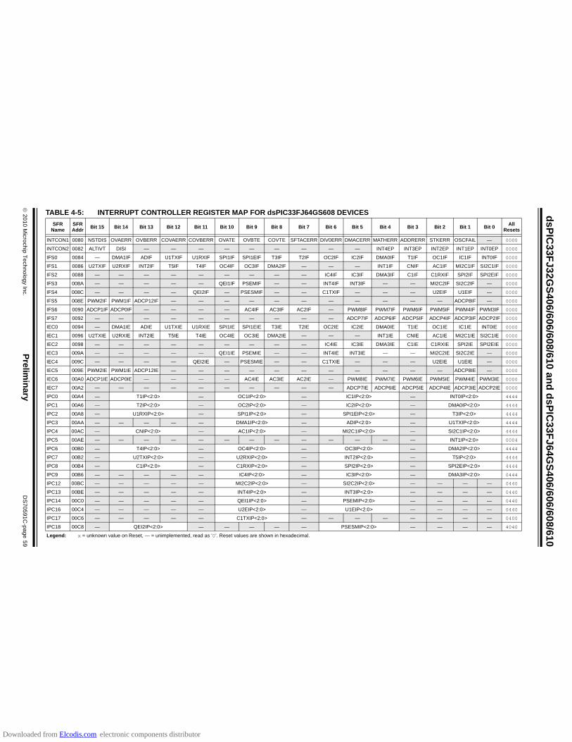
2
01
0 M
icroch
ip T
ech
no
log
y Inc.
Prelim
inary
DS
70
59
1C
-pa
ge
59
ds
PIC
33
FJ
32
GS
40
6/6
06/6
08/6
10 a
nd
ds
PIC
33
FJ
64G
S4
06/6
06/60
8/61
0
TABLE 4-5: INTERRUPT CONTROLLER REGISTER MAP FOR dsPIC33FJ64GS608 DEVICES
SFR Name
SFRAddr
Bit 15 Bit 14 Bit 13 Bit 12 Bit 11 Bit 10 Bit 9 Bit 8 Bit 7 Bit 6 Bit 5 Bit 4 Bit 3 Bit 2 Bit 1 Bit 0All
Resets
INTCON1 0080 NSTDIS OVAERR OVBERR COVAERR COVBERR OVATE OVBTE COVTE SFTACERR DIV0ERR DMACERR MATHERR ADDRERR STKERR OSCFAIL — 0000
INTCON2 0082 ALTIVT DISI — — — — — — — — — INT4EP INT3EP INT2EP INT1EP INT0EP 0000
IFS0 0084 — DMA1IF ADIF U1TXIF U1RXIF SPI1IF SPI1EIF T3IF T2IF OC2IF IC2IF DMA0IF T1IF OC1IF IC1IF INT0IF 0000
IFS1 0086 U2TXIF U2RXIF INT2IF T5IF T4IF OC4IF OC3IF DMA2IF — — — INT1IF CNIF AC1IF MI2C1IF SI2C1IF 0000
IFS2 0088 — — — — — — — — — IC4IF IC3IF DMA3IF C1IF C1RXIF SPI2IF SPI2EIF 0000
IFS3 008A — — — — — QEI1IF PSEMIF — — INT4IF INT3IF — — MI2C2IF SI2C2IF — 0000
IFS4 008C — — — — QEI2IF — PSESMIF — — C1TXIF — — — U2EIF U1EIF — 0000
IFS5 008E PWM2IF PWM1IF ADCP12IF — — — — — — — — — — — ADCP8IF — 0000
IFS6 0090 ADCP1IF ADCP0IF — — — — AC4IF AC3IF AC2IF — PWM8IF PWM7IF PWM6IF PWM5IF PWM4IF PWM3IF 0000
IFS7 0092 — — — — — — — — — — ADCP7IF ADCP6IF ADCP5IF ADCP4IF ADCP3IF ADCP2IF 0000
IEC0 0094 — DMA1IE ADIE U1TXIE U1RXIE SPI1IE SPI1EIE T3IE T2IE OC2IE IC2IE DMA0IE T1IE OC1IE IC1IE INT0IE 0000
IEC1 0096 U2TXIE U2RXIE INT2IE T5IE T4IE OC4IE OC3IE DMA2IE — — — INT1IE CNIE AC1IE MI2C1IE SI2C1IE 0000
IEC2 0098 — — — — — — — — — IC4IE IC3IE DMA3IE C1IE C1RXIE SPI2IE SPI2EIE 0000
IEC3 009A — — — — — QEI1IE PSEMIE — — INT4IE INT3IE — — MI2C2IE SI2C2IE — 0000
IEC4 009C — — — — QEI2IE — PSESMIE — — C1TXIE — — — U2EIE U1EIE — 0000
IEC5 009E PWM2IE PWM1IE ADCP12IE — — — — — — — — — — — ADCP8IE — 0000
IEC6 00A0 ADCP1IE ADCP0IE — — — — AC4IE AC3IE AC2IE — PWM8IE PWM7IE PWM6IE PWM5IE PWM4IE PWM3IE 0000
IEC7 00A2 — — — — — — — — — — ADCP7IE ADCP6IE ADCP5IE ADCP4IE ADCP3IE ADCP2IE 0000
IPC0 00A4 — T1IP<2:0> — OC1IP<2:0> — IC1IP<2:0> — INT0IP<2:0> 4444
IPC1 00A6 — T2IP<2:0> — OC2IP<2:0> — IC2IP<2:0> — DMA0IP<2:0> 4444
IPC2 00A8 — U1RXIP<2:0> — SPI1IP<2:0> — SPI1EIP<2:0> — T3IP<2:0> 4444
IPC3 00AA — — — — — DMA1IP<2:0> — ADIP<2:0> — U1TXIP<2:0> 4444
IPC4 00AC — CNIP<2:0> — AC1IP<2:0> — MI2C1IP<2:0> — SI2C1IP<2:0> 4444
IPC5 00AE — — — — — — — — — — — — — INT1IP<2:0> 0004
IPC6 00B0 — T4IP<2:0> — OC4IP<2:0> — OC3IP<2:0> — DMA2IP<2:0> 4444
IPC7 00B2 — U2TXIP<2:0> — U2RXIP<2:0> — INT2IP<2:0> — T5IP<2:0> 4444
IPC8 00B4 — C1IP<2:0> — C1RXIP<2:0> — SPI2IP<2:0> — SPI2EIP<2:0> 4444
IPC9 00B6 — — — — — IC4IP<2:0> — IC3IP<2:0> — DMA3IP<2:0> 0444
IPC12 00BC — — — — — MI2C2IP<2:0> — SI2C2IP<2:0> — — — — 0440
IPC13 00BE — — — — — INT4IP<2:0> — INT3IP<2:0> — — — — 0440
IPC14 00C0 — — — — — QEI1IP<2:0> — PSEMIP<2:0> — — — — 0440
IPC16 00C4 — — — — — U2EIP<2:0> — U1EIP<2:0> — — — — 0440
IPC17 00C6 — — — — — C1TXIP<2:0> — — — — — — — — 0400
IPC18 00C8 — QEI2IP<2:0> — — — — — PSESMIP<2:0> — — — — 4040
Legend: x = unknown value on Reset, — = unimplemented, read as ‘0’. Reset values are shown in hexadecimal.
Downloaded from Elcodis.com electronic components distributor

ds
PIC
33
FJ
32
GS
40
6/6
06
/60
8/6
10
an
d d
sP
IC3
3F
J6
4G
S4
06
/60
6/6
08/6
10
DS
70
59
1C
-pa
ge
60
Prelim
ina
ry
20
10
Micro
chip
Te
chn
olo
gy In
c.
IPC20 00CC — — — — — — — — — ADCP8IP<2:0> — — — — 0040
IPC21 00CE — — — — — — — — — ADCP12IP — — — — 0040
IPC23 00D2 — PWM2IP<2:0> — PWM1IP<2:0> — — — — — — — — 4400
IPC24 00D4 — PWM6IP<2:0> — PWM5IP<2:0> — PWM4IP<2:0> — PWM3IP<2:0> 4444
IPC25 00D6 — AC2IP<2:0> — — — — — PWM8IP<2:0> — PWM7IP<2:0> 4044
IPC26 00D8 — — — — — — — — — AC4IP<2:0> — AC3IP<2:0> 0044
IPC27 00DA — ADCP1IP<2:0> — ADCP0IP<2:0> — — — — — — — — 4400
IPC28 00DC — ADCP5IP<2:0> — ADCP4IP<2:0> — ADCP3IP<2:0> — ADCP2IP<2:0> 4444
IPC29 00DE — — — — — — — — — ADCP7IP<2:0> — ADCP6IP<2:0> 0044
INTTREG 00E0 — — — — ILR<3:0> — VECNUM<6:0> 0000
TABLE 4-5: INTERRUPT CONTROLLER REGISTER MAP FOR dsPIC33FJ64GS608 DEVICES (CONTINUED)
SFR Name
SFRAddr
Bit 15 Bit 14 Bit 13 Bit 12 Bit 11 Bit 10 Bit 9 Bit 8 Bit 7 Bit 6 Bit 5 Bit 4 Bit 3 Bit 2 Bit 1 Bit 0All
Resets
Legend: x = unknown value on Reset, — = unimplemented, read as ‘0’. Reset values are shown in hexadecimal.
Downloaded from Elcodis.com electronic components distributor

2
01
0 M
icroch
ip T
ech
no
log
y Inc.
Prelim
inary
DS
70
59
1C
-pa
ge
61
ds
PIC
33
FJ
32
GS
40
6/6
06/6
08/6
10 a
nd
ds
PIC
33
FJ
64G
S4
06/6
06/60
8/61
0
TABLE 4-6: INTERRUPT CONTROLLER REGISTER MAP FOR dsPIC33FJ64GS606 DEVICES
SFR Name
SFRAddr
Bit 15 Bit 14 Bit 13 Bit 12 Bit 11 Bit 10 Bit 9 Bit 8 Bit 7 Bit 6 Bit 5 Bit 4 Bit 3 Bit 2 Bit 1 Bit 0All
Resets
INTCON1 0080 NSTDIS OVAERR OVBERR COVAERR COVBERR OVATE OVBTE COVTE SFTACERR DIV0ERR DMACERR MATHERR ADDRERR STKERR OSCFAIL — 0000
INTCON2 0082 ALTIVT DISI — — — — — — — — — INT4EP INT3EP INT2EP INT1EP INT0EP 0000
IFS0 0084 — DMA1IF ADIF U1TXIF U1RXIF SPI1IF SPI1EIF T3IF T2IF OC2IF IC2IF DMA0IF T1IF OC1IF IC1IF INT0IF 0000
IFS1 0086 U2TXIF U2RXIF INT2IF T5IF T4IF OC4IF OC3IF DMA2IF — — — INT1IF CNIF AC1IF MI2C1IF SI2C1IF 0000
IFS2 0088 — — — — — — — — — IC4IF IC3IF DMA3IF C1IF C1RXIF SPI2IF SPI2EIF 0000
IFS3 008A — — — — — QEI1IF PSEMIF — — INT4IF INT3IF — — MI2C2IF SI2C2IF — 0000
IFS4 008C — — — — QEI2IF — PSESMIF — — C1TXIF — — — U2EIF U1EIF — 0000
IFS5 008E PWM2IF PWM1IF ADCP12IF — — — — — — — — — — — ADCP8IF — 0000
IFS6 0090 ADCP1IF ADCP0IF — — — — AC4IF AC3IF AC2IF — — — PWM6IF PWM5IF PWM4IF PWM3IF 0000
IFS7 0092 — — — — — — — — — — — ADCP6IF ADCP5IF ADCP4IF ADCP3IF ADCP2IF 0000
IEC0 0094 — DMA1IE ADIE U1TXIE U1RXIE SPI1IE SPI1EIE T3IE T2IE OC2IE IC2IE DMA0IE T1IE OC1IE IC1IE INT0IE 0000
IEC1 0096 U2TXIE U2RXIE INT2IE T5IE T4IE OC4IE OC3IE DMA2IE — — — INT1IE CNIE AC1IE MI2C1IE SI2C1IE 0000
IEC2 0098 — — — — — — — — — IC4IE IC3IE DMA3IE C1IE C1RXIE SPI2IE SPI2EIE 0000
IEC3 009A — — — — — QEI1IE PSEMIE — — INT4IE INT3IE — — MI2C2IE SI2C2IE — 0000
IEC4 009C — — — — QEI2IE — PSESMIE — — C1TXIE — — — U2EIE U1EIE — 0000
IEC5 009E PWM2IE PWM1IE ADCP12IE — — — — — — — — — — — ADCP8IE — 0000
IEC6 00A0 ADCP1IE ADCP0IE — — — — AC4IE AC3IE AC2IE — — — PWM6IE PWM5IE PWM4IE PWM3IE 0000
IEC7 00A2 — — — — — — — — — — — ADCP6IE ADCP5IE ADCP4IE ADCP3IE ADCP2IE 0000
IPC0 00A4 — T1IP<2:0> — OC1IP<2:0> — IC1IP<2:0> — INT0IP<2:0> 4444
IPC1 00A6 — T2IP<2:0> — OC2IP<2:0> — IC2IP<2:0> — DMA0IP<2:0> 4444
IPC2 00A8 — U1RXIP<2:0> — SPI1IP<2:0> — SPI1EIP<2:0> — T3IP<2:0> 4444
IPC3 00AA — — — — — DMA1IP<2:0> — ADIP<2:0> — U1TXIP<2:0> 4444
IPC4 00AC — CNIP<2:0> — AC1IP<2:0> — MI2C1IP<2:0> — SI2C1IP<2:0> 4444
IPC5 00AE — — — — — — — — — — — — — INT1IP<2:0> 0004
IPC6 00B0 — T4IP<2:0> — OC4IP<2:0> — OC3IP<2:0> — DMA2IP<2:0> 4444
IPC7 00B2 — U2TXIP<2:0> — U2RXIP<2:0> — INT2IP<2:0> — T5IP<2:0> 4444
IPC8 00B4 — C1IP<2:0> — C1RXIP<2:0> — SPI2IP<2:0> — SPI2EIP<2:0> 4444
IPC9 00B6 — — — — — IC4IP<2:0> — IC3IP<2:0> — DMA3IP<2:0> 0444
IPC12 00BC — — — — — MI2C2IP<2:0> — SI2C2IP<2:0> — — — — 0440
IPC13 00BE — — — — — INT4IP<2:0> — INT3IP<2:0> — — — — 0440
IPC14 00C0 — — — — — QEI1IP<2:0> — PSEMIP<2:0> — — — — 0440
IPC16 00C4 — — — — — U2EIP<2:0> — U1EIP<2:0> — — — — 0440
IPC17 00C6 — — — — — C1TXIP<2:0> — — — — — — — — 0400
IPC18 00C8 — QEI2IP<2:0> — — — — — PSESMIP<2:0> — — — — 4040
Legend: x = unknown value on Reset, — = unimplemented, read as ‘0’. Reset values are shown in hexadecimal.
Downloaded from Elcodis.com electronic components distributor
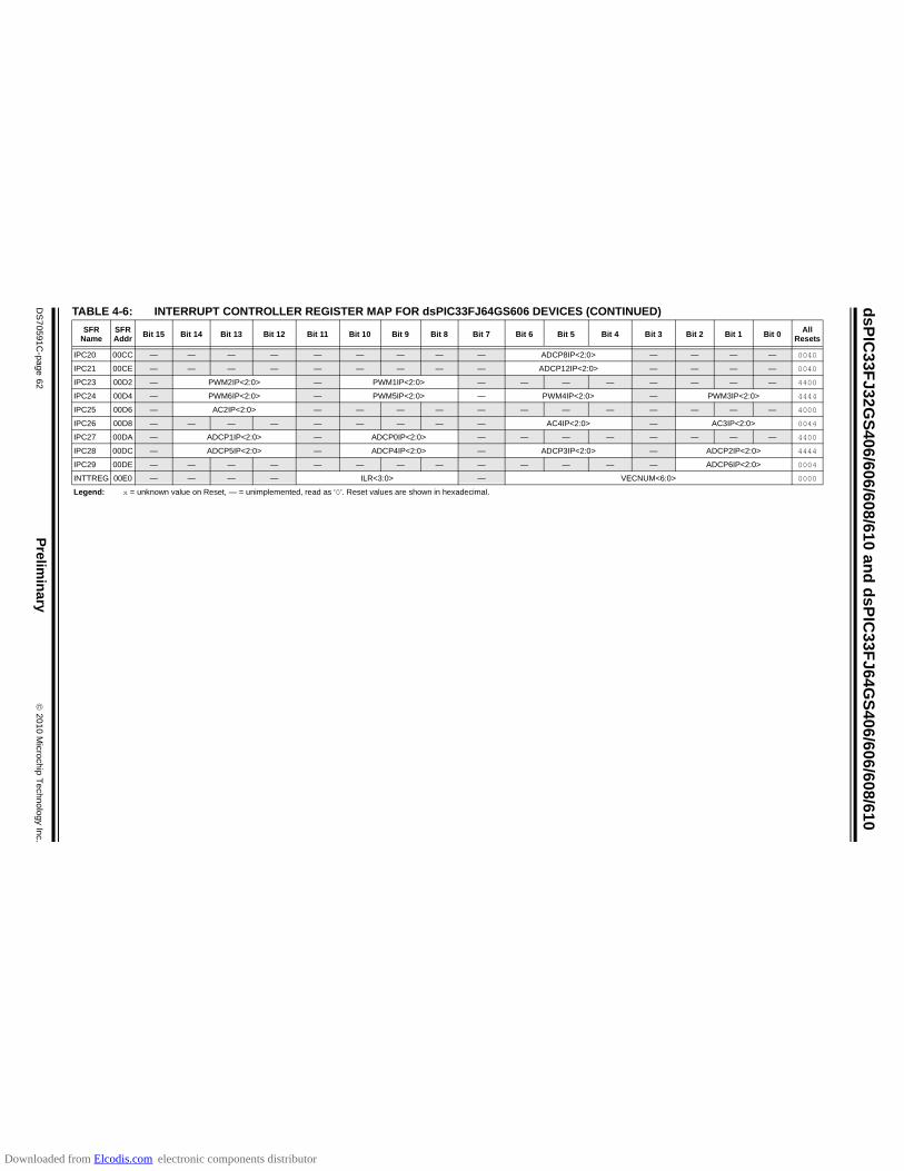
ds
PIC
33
FJ
32
GS
40
6/6
06
/60
8/6
10
an
d d
sP
IC3
3F
J6
4G
S4
06
/60
6/6
08/6
10
DS
70
59
1C
-pa
ge
62
Prelim
ina
ry
20
10
Micro
chip
Te
chn
olo
gy In
c.
IPC20 00CC — — — — — — — — — ADCP8IP<2:0> — — — — 0040
IPC21 00CE — — — — — — — — — ADCP12IP<2:0> — — — — 0040
IPC23 00D2 — PWM2IP<2:0> — PWM1IP<2:0> — — — — — — — — 4400
IPC24 00D4 — PWM6IP<2:0> — PWM5IP<2:0> — PWM4IP<2:0> — PWM3IP<2:0> 4444
IPC25 00D6 — AC2IP<2:0> — — — — — — — — — — — — 4000
IPC26 00D8 — — — — — — — — — AC4IP<2:0> — AC3IP<2:0> 0044
IPC27 00DA — ADCP1IP<2:0> — ADCP0IP<2:0> — — — — — — — — 4400
IPC28 00DC — ADCP5IP<2:0> — ADCP4IP<2:0> — ADCP3IP<2:0> — ADCP2IP<2:0> 4444
IPC29 00DE — — — — — — — — — — — — — ADCP6IP<2:0> 0004
INTTREG 00E0 — — — — ILR<3:0> — VECNUM<6:0> 0000
TABLE 4-6: INTERRUPT CONTROLLER REGISTER MAP FOR dsPIC33FJ64GS606 DEVICES (CONTINUED)
SFR Name
SFRAddr
Bit 15 Bit 14 Bit 13 Bit 12 Bit 11 Bit 10 Bit 9 Bit 8 Bit 7 Bit 6 Bit 5 Bit 4 Bit 3 Bit 2 Bit 1 Bit 0All
Resets
Legend: x = unknown value on Reset, — = unimplemented, read as ‘0’. Reset values are shown in hexadecimal.
Downloaded from Elcodis.com electronic components distributor
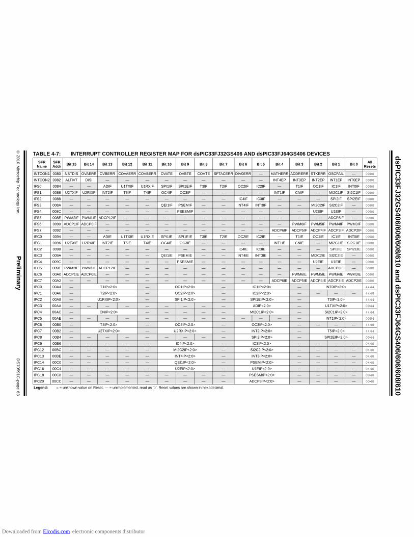
2
01
0 M
icroch
ip T
ech
no
log
y Inc.
Prelim
inary
DS
70
59
1C
-pa
ge
63
ds
PIC
33
FJ
32
GS
40
6/6
06/6
08/6
10 a
nd
ds
PIC
33
FJ
64G
S4
06/6
06/60
8/61
0
TABLE 4-7: INTERRUPT CONTROLLER REGISTER MAP FOR dsPIC33FJ32GS406 AND dsPIC33FJ64GS406 DEVICES
SFR Name
SFRAddr
Bit 15 Bit 14 Bit 13 Bit 12 Bit 11 Bit 10 Bit 9 Bit 8 Bit 7 Bit 6 Bit 5 Bit 4 Bit 3 Bit 2 Bit 1 Bit 0All
Resets
INTCON1 0080 NSTDIS OVAERR OVBERR COVAERR COVBERR OVATE OVBTE COVTE SFTACERR DIV0ERR — MATHERR ADDRERR STKERR OSCFAIL — 0000
INTCON2 0082 ALTIVT DISI — — — — — — — — — INT4EP INT3EP INT2EP INT1EP INT0EP 0000
IFS0 0084 — — ADIF U1TXIF U1RXIF SPI1IF SPI1EIF T3IF T2IF OC2IF IC2IF — T1IF OC1IF IC1IF INT0IF 0000
IFS1 0086 U2TXIF U2RXIF INT2IF T5IF T4IF OC4IF OC3IF — — — — INT1IF CNIF — MI2C1IF SI2C1IF 0000
IFS2 0088 — — — — — — — — — IC4IF IC3IF — — — SPI2IF SPI2EIF 0000
IFS3 008A — — — — — QEI1IF PSEMIF — — INT4IF INT3IF — — MI2C2IF SI2C2IF — 0000
IFS4 008C — — — — — — PSESMIF — — — — — — U2EIF U1EIF — 0000
IFS5 008E PWM2IF PWM1IF ADCP12IF — — — — — — — — — — — ADCP8IF — 0000
IFS6 0090 ADCP1IF ADCP0IF — — — — — — — — — — PWM6IF PWM5IF PWM4IF PWM3IF 0000
IFS7 0092 — — — — — — — — — — — ADCP6IF ADCP5IF ADCP4IF ADCP3IF ADCP2IF 0000
IEC0 0094 — — ADIE U1TXIE U1RXIE SPI1IE SPI1EIE T3IE T2IE OC2IE IC2IE — T1IE OC1IE IC1IE INT0IE 0000
IEC1 0096 U2TXIE U2RXIE INT2IE T5IE T4IE OC4IE OC3IE — — — — INT1IE CNIE — MI2C1IE SI2C1IE 0000
IEC2 0098 — — — — — — — — — IC4IE IC3IE — — — SPI2IE SPI2EIE 0000
IEC3 009A — — — — — QEI1IE PSEMIE — — INT4IE INT3IE — — MI2C2IE SI2C2IE — 0000
IEC4 009C — — — — — — PSESMIE — — — — — — U2EIE U1EIE — 0000
IEC5 009E PWM2IE PWM1IE ADCP12IE — — — — — — — — — — — ADCP8IE — 0000
IEC6 00A0 ADCP1IE ADCP0IE — — — — — — — — — — PWM6IE PWM5IE PWM4IE PWM3IE 0000
IEC7 00A2 — — — — — — — — — — — ADCP6IE ADCP5IE ADCP4IE ADCP3IE ADCP2IE 0000
IPC0 00A4 — T1IP<2:0> — OC1IP<2:0> — IC1IP<2:0> — INT0IP<2:0> 4444
IPC1 00A6 — T2IP<2:0> — OC2IP<2:0> — IC2IP<2:0> — — — — 4440
IPC2 00A8 — U1RXIP<2:0> — SPI1IP<2:0> — SPI1EIP<2:0> — T3IP<2:0> 4444
IPC3 00AA — — — — — — — — — ADIP<2:0> — U1TXIP<2:0> 0044
IPC4 00AC — CNIP<2:0> — — — — — MI2C1IP<2:0> — SI2C1IP<2:0> 4444
IPC5 00AE — — — — — — — — — — — — — INT1IP<2:0> 0004
IPC6 00B0 — T4IP<2:0> — OC4IP<2:0> — OC3IP<2:0> — — — — 4440
IPC7 00B2 — U2TXIP<2:0> — U2RXIP<2:0> — INT2IP<2:0> — T5IP<2:0> 4444
IPC8 00B4 — — — — — — — — — SPI2IP<2:0> — SPI2EIP<2:0> 0044
IPC9 00B6 — — — — — IC4IP<2:0> — IC3IP<2:0> — — — — 0440
IPC12 00BC — — — — — MI2C2IP<2:0> — SI2C2IP<2:0> — — — — 0440
IPC13 00BE — — — — — INT4IP<2:0> — INT3IP<2:0> — — — — 0440
IPC14 00C0 — — — — — QEI1IP<2:0> — PSEMIP<2:0> — — — — 0440
IPC16 00C4 — — — — — U2EIP<2:0> — U1EIP<2:0> — — — — 0440
IPC18 00C8 — — — — — — — — — PSESMIP<2:0> — — — — 0040
IPC20 00CC — — — — — — — — — ADCP8IP<2:0> — — — — 0040
Legend: x = unknown value on Reset, — = unimplemented, read as ‘0’. Reset values are shown in hexadecimal.
Downloaded from Elcodis.com electronic components distributor
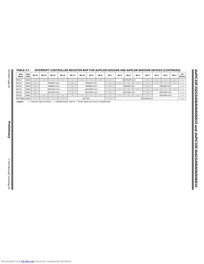
ds
PIC
33
FJ
32
GS
40
6/6
06
/60
8/6
10
an
d d
sP
IC3
3F
J6
4G
S4
06
/60
6/6
08/6
10
DS
70
59
1C
-pa
ge
64
Prelim
ina
ry
20
10
Micro
chip
Te
chn
olo
gy In
c.
IPC21 00CE — — — — — — — — — ADCP12IP<2:0> — — — — 0040
IPC23 00D2 — PWM2IP<2:0> — PWM1IP<2:0> — — — — — — — — 4400
IPC24 00D4 — PWM6IP<2:0> — PWM5IP<2:0> — PWM4IP<2:0> — PWM3IP<2:0> 4444
IPC27 00DA — ADCP1IP<2:0> — ADCP0IP<2:0> — — — — — — — — 4400
IPC28 00DC — ADCP5IP<2:0> — ADCP4IP<2:0> — ADCP3IP<2:0> — ADCP2IP<2:0> 4444
IPC29 00DE — — — — — — — — — — — — — ADCP6IP<2:0> 0004
INTTREG 00E0 — — — — ILR<3:0> — VECNUM<6:0> 0000
TABLE 4-7: INTERRUPT CONTROLLER REGISTER MAP FOR dsPIC33FJ32GS406 AND dsPIC33FJ64GS406 DEVICES (CONTINUED)
SFR Name
SFRAddr
Bit 15 Bit 14 Bit 13 Bit 12 Bit 11 Bit 10 Bit 9 Bit 8 Bit 7 Bit 6 Bit 5 Bit 4 Bit 3 Bit 2 Bit 1 Bit 0All
Resets
Legend: x = unknown value on Reset, — = unimplemented, read as ‘0’. Reset values are shown in hexadecimal.
Downloaded from Elcodis.com electronic components distributor

2
01
0 M
icroch
ip T
ech
no
log
y Inc.
Prelim
inary
DS
70
59
1C
-pa
ge
65
ds
PIC
33
FJ
32
GS
40
6/6
06/6
08/6
10 a
nd
ds
PIC
33
FJ
64G
S4
06/6
06/60
8/61
0
TABLE 4-8: INTERRUPT CONTROLLER REGISTER MAP FOR dsPIC33FJ32GS610 DEVICES
SFR Name
SFR Addr
Bit 15 Bit 14 Bit 13 Bit 12 Bit 11 Bit 10 Bit 9 Bit 8 Bit 7 Bit 6 Bit 5 Bit 4 Bit 3 Bit 2 Bit 1 Bit 0All
Resets
INTCON1 0080 NSTDIS OVAERR OVBERR COVAERR COVBERR OVATE OVBTE COVTE SFTACERR DIV0ERR — MATHERR ADDRERR STKERR OSCFAIL — 0000
INTCON2 0082 ALTIVT DISI — — — — — — — — — INT4EP INT3EP INT2EP INT1EP INT0EP 0000
IFS0 0084 — — ADIF U1TXIF U1RXIF SPI1IF SPI1EIF T3IF T2IF OC2IF IC2IF — T1IF OC1IF IC1IF INT0IF 0000
IFS1 0086 U2TXIF U2RXIF INT2IF T5IF T4IF OC4IF OC3IF — — — — INT1IF CNIF AC1IF MI2C1IF SI2C1IF 0000
IFS2 0088 — — — — — — — — — IC4IF IC3IF — — — SPI2IF SPI2EIF 0000
IFS3 008A — — — — — QEI1IF PSEMIF — — INT4IF INT3IF — — MI2C2IF SI2C2IF — 0000
IFS4 008C — — — — QEI2IF — PSESMIF — — — — — — U2EIF U1EIF — 0000
IFS5 008E PWM2IF PWM1IF ADCP12IF — — — — — — — — ADCP11IF ADCP10IF ADCP9IF ADCP8IF — 0000
IFS6 0090 ADCP1IF ADCP0IF — — — — AC4IF AC3IF AC2IF PWM9IF PWM8IF PWM7IF PWM6IF PWM5IF PWM4IF PWM3IF 0000
IFS7 0092 — — — — — — — — — — ADCP7IF ADCP6IF ADCP5IF ADCP4IF ADCP3IF ADCP2IF 0000
IEC0 0094 — — ADIE U1TXIE U1RXIE SPI1IE SPI1EIE T3IE T2IE OC2IE IC2IE — T1IE OC1IE IC1IE INT0IE 0000
IEC1 0096 U2TXIE U2RXIE INT2IE T5IE T4IE OC4IE OC3IE — — — — INT1IE CNIE AC1IE MI2C1IE SI2C1IE 0000
IEC2 0098 — — — — — — — — — IC4IE IC3IE — — — SPI2IE SPI2EIE 0000
IEC3 009A — — — — — QEI1IE PSEMIE — — INT4IE INT3IE — — MI2C2IE SI2C2IE — 0000
IEC4 009C — — — — QEI2IE — PSESMIE — — — — — — U2EIE U1EIE — 0000
IEC5 009E PWM2IE PWM1IE ADCP12IE — — — — — — — — ADCP11IE ADCP10IE ADCP9IE ADCP8IE — 0000
IEC6 00A0 ADCP1IE ADCP0IE — — — — AC4IE AC3IE AC2IE PWM9IE PWM8IE PWM7IE PWM6IE PWM5IE PWM4IE PWM3IE 0000
IEC7 00A2 — — — — — — — — — — ADCP7IE ADCP6IE ADCP5IE ADCP4IE ADCP3IE ADCP2IE 0000
IPC0 00A4 — T1IP<2:0> — OC1IP<2:0> — IC1IP<2:0> — INT0IP<2:0> 4444
IPC1 00A6 — T2IP<2:0> — OC2IP<2:0> — IC2IP<2:0> — — — — 4440
IPC2 00A8 — U1RXIP<2:0> — SPI1IP<2:0> — SPI1EIP<2:0> — T3IP<2:0> 4444
IPC3 00AA — — — — — — — — — ADIP<2:0> — U1TXIP<2:0> 0044
IPC4 00AC — CNIP<2:0> — AC1IP<2:0> — MI2C1IP<2:0> — SI2C1IP<2:0> 4444
IPC5 00AE — — — — — — — — — — — — — INT1IP<2:0> 0004
IPC6 00B0 — T4IP<2:0> — OC4IP<2:0> — OC3IP<2:0> — — — — 4440
IPC7 00B2 — U2TXIP<2:0> — U2RXIP<2:0> — INT2IP<2:0> — T5IP<2:0> 4444
IPC8 00B4 — — — — — — — — — SPI2IP<2:0> — SPI2EIP<2:0> 0044
IPC9 00B6 — — — — — IC4IP<2:0> — IC3IP<2:0> — — — — 0440
IPC12 00BC — — — — — MI2C2IP<2:0> — SI2C2IP<2:0> — — — — 0440
IPC13 00BE — — — — — INT4IP<2:0> — INT3IP<2:0> — — — — 0440
IPC14 00C0 — — — — — QEI1IP<2:0> — PSEMIP<2:0> — — — — 0440
IPC16 00C4 — — — — — U2EIP<2:0> — U1EIP<2:0> — — — — 0440
IPC18 00C8 — QEI2IP<2:0> — — — — — PSESMIP<2:0> — — — — 4040
IPC20 00CC — ADCP10IP<2:0> — ADCP9IP<2:0> — ADCP8IP<2:0> — — — — 4440
Legend: x = unknown value on Reset, — = unimplemented, read as ‘0’. Reset values are shown in hexadecimal.
Downloaded from Elcodis.com electronic components distributor

ds
PIC
33
FJ
32
GS
40
6/6
06
/60
8/6
10
an
d d
sP
IC3
3F
J6
4G
S4
06
/60
6/6
08/6
10
DS
70
59
1C
-pa
ge
66
Prelim
ina
ry
20
10
Micro
chip
Te
chn
olo
gy In
c.
IPC21 00CE — — — — — — — — — ADCP12IP<2:0> — ADCP11IP<2:0> 0044
IPC23 00D2 — PWM2IP<2:0> — PWM1IP<2:0> — — — — — — — — 4400
IPC24 00D4 — PWM6IP<2:0> — PWM5IP<2:0> — PWM4IP<2:0> — PWM3IP<2:0> 4444
IPC25 00D6 — AC2IP<2:0> — PWM9IP<2:0> — PWM8IP<2:0> — PWM7IP<2:0> 4444
IPC26 00D8 — — — — — — — — — AC4IP<2:0> — AC3IP<2:0> 0044
IPC27 00DA — ADCP1IP<2:0> — ADCP0IP<2:0> — — — — — — — — 4400
IPC28 00DC — ADCP5IP<2:0> — ADCP4IP<2:0> — ADCP3IP<2:0> — ADCP2IP<2:0> 4444
IPC29 00DE — — — — — — — — — ADCP7IP<2:0> — ADCP6IP<2:0> 0044
INTTREG 00E0 — — — — ILR<3:0> — VECNUM<6:0> 0000
TABLE 4-8: INTERRUPT CONTROLLER REGISTER MAP FOR dsPIC33FJ32GS610 DEVICES (CONTINUED)
SFR Name
SFR Addr
Bit 15 Bit 14 Bit 13 Bit 12 Bit 11 Bit 10 Bit 9 Bit 8 Bit 7 Bit 6 Bit 5 Bit 4 Bit 3 Bit 2 Bit 1 Bit 0All
Resets
Legend: x = unknown value on Reset, — = unimplemented, read as ‘0’. Reset values are shown in hexadecimal.
Downloaded from Elcodis.com electronic components distributor

2
01
0 M
icroch
ip T
ech
no
log
y Inc.
Prelim
inary
DS
70
59
1C
-pa
ge
67
ds
PIC
33
FJ
32
GS
40
6/6
06/6
08/6
10 a
nd
ds
PIC
33
FJ
64G
S4
06/6
06/60
8/61
0
TABLE 4-9: INTERRUPT CONTROLLER REGISTER MAP FOR dsPIC33FJ32GS608
SFR Name
SFR Addr
Bit 15 Bit 14 Bit 13 Bit 12 Bit 11 Bit 10 Bit 9 Bit 8 Bit 7 Bit 6 Bit 5 Bit 4 Bit 3 Bit 2 Bit 1 Bit 0All
Resets
INTCON1 0080 NSTDIS OVAERR OVBERR COVAERR COVBERR OVATE OVBTE COVTE SFTACERR DIV0ERR — MATHERR ADDRERR STKERR OSCFAIL — 0000
INTCON2 0082 ALTIVT DISI — — — — — — — — — INT4EP INT3EP INT2EP INT1EP INT0EP 0000
IFS0 0084 — — ADIF U1TXIF U1RXIF SPI1IF SPI1EIF T3IF T2IF OC2IF IC2IF — T1IF OC1IF IC1IF INT0IF 0000
IFS1 0086 U2TXIF U2RXIF INT2IF T5IF T4IF OC4IF OC3IF — — — — INT1IF CNIF AC1IF MI2C1IF SI2C1IF 0000
IFS2 0088 — — — — — — — — — IC4IF IC3IF — — — SPI2IF SPI2EIF 0000
IFS3 008A — — — — — QEI1IF PSEMIF — — INT4IF INT3IF — — MI2C2IF SI2C2IF — 0000
IFS4 008C — — — — QEI2IF — PSESMIF — — — — — — U2EIF U1EIF — 0000
IFS5 008E PWM2IF PWM1IF ADCP12IF — — — — — — — — — — — ADCP8IF — 0000
IFS6 0090 ADCP1IF ADCP0IF — — — — AC4IF AC3IF AC2IF — PWM8IF PWM7IF PWM6IF PWM5IF PWM4IF PWM3IF 0000
IFS7 0092 — — — — — — — — — — ADCP7IF ADCP6IF ADCP5IF ADCP4IF ADCP3IF ADCP2IF 0000
IEC0 0094 — — ADIE U1TXIE U1RXIE SPI1IE SPI1EIE T3IE T2IE OC2IE IC2IE — T1IE OC1IE IC1IE INT0IE 0000
IEC1 0096 U2TXIE U2RXIE INT2IE T5IE T4IE OC4IE OC3IE — — — — INT1IE CNIE — MI2C1IE SI2C1IE 0000
IEC2 0098 — — — — — — — — — IC4IE IC3IE — — — SPI2IE SPI2EIE 0000
IEC3 009A — — — — — QEI1IE PSEMIE — — INT4IE INT3IE — — MI2C2IE SI2C2IE — 0000
IEC4 009C — — — — QEI2IE — PSESMIE — — — — — — U2EIE U1EIE — 0000
IEC5 009E PWM2IE PWM1IE ADCP12IE — — — — — — — — — — — ADCP8IE — 0000
IEC6 00A0 ADCP1IE ADCP0IE — — — — AC4IE AC3IE AC2IE — PWM8IE PWM7IE PWM6IE PWM5IE PWM4IE PWM3IE 0000
IEC7 00A2 — — — — — — — — — — ADCP7IE ADCP6IE ADCP5IE ADCP4IE ADCP3IE ADCP2IE 0000
IPC0 00A4 — T1IP<2:0> — OC1IP<2:0> — IC1IP<2:0> — INT0IP<2:0> 4444
IPC1 00A6 — T2IP<2:0> — OC2IP<2:0> — IC2IP<2:0> — — — — 4440
IPC2 00A8 — U1RXIP<2:0> — SPI1IP<2:0> — SPI1EIP<2:0> — T3IP<2:0> 4444
IPC3 00AA — — — — — — — — — ADIP<2:0> — U1TXIP<2:0> 0044
IPC4 00AC — CNIP<2:0> — AC1IP<2:0> — MI2C1IP<2:0> — SI2C1IP<2:0> 4444
IPC5 00AE — — — — — — — — — — — — — INT1IP<2:0> 0004
IPC6 00B0 — T4IP<2:0> — OC4IP<2:0> — OC3IP<2:0> — — — — 4440
IPC7 00B2 — U2TXIP<2:0> — U2RXIP<2:0> — INT2IP<2:0> — T5IP<2:0> 4444
IPC8 00B4 — — — — — — — — — SPI2IP<2:0> — SPI2EIP<2:0> 0044
IPC9 00B6 — — — — — IC4IP<2:0> — IC3IP<2:0> — — — — 0440
IPC12 00BC — — — — — MI2C2IP<2:0> — SI2C2IP<2:0> — — — — 0440
IPC13 00BE — — — — — INT4IP<2:0> — INT3IP<2:0> — — — — 0440
IPC14 00C0 — — — — — QEI1IP<2:0> — PSEMIP<2:0> — — — — 0440
IPC16 00C4 — — — — — U2EIP<2:0> — U1EIP<2:0> — — — — 0440
IPC18 00C8 — QEI2IP<2:0> — — — — — PSESMIP<2:0> — — — — 4040
IPC20 00CC — — — — — — — — — ADCP8IP<2:0> — — — — 0040
Legend: x = unknown value on Reset, — = unimplemented, read as ‘0’. Reset values are shown in hexadecimal.
Downloaded from Elcodis.com electronic components distributor

ds
PIC
33
FJ
32
GS
40
6/6
06
/60
8/6
10
an
d d
sP
IC3
3F
J6
4G
S4
06
/60
6/6
08/6
10
DS
70
59
1C
-pa
ge
68
Prelim
ina
ry
20
10
Micro
chip
Te
chn
olo
gy In
c.
IPC21 00CE — — — — — — — — — ADCP12IP<2:0> — — — — 0040
IPC23 00D2 — PWM2IP<2:0> — PWM1IP<2:0> — — — — — — — — 4400
IPC24 00D4 — PWM6IP<2:0> — PWM5IP<2:0> — PWM4IP<2:0> — PWM3IP<2:0> 4444
IPC25 00D6 — AC2IP<2:0> — — — — — PWM8IP<2:0> — PWM7IP<2:0> 4044
IPC26 00D8 — — — — — — — — — AC4IP<2:0> — AC3IP<2:0> 0044
IPC27 00DA — ADCP1IP<2:0> — ADCP0IP<2:0> — — — — — — — — 4400
IPC28 00DC — ADCP5IP<2:0> — ADCP4IP<2:0> — ADCP3IP<2:0> — ADCP2IP<2:0> 4444
IPC29 00DE — — — — — — — — — ADCP7IP<2:0> — ADCP6IP<2:0> 0044
INTTREG 00E0 — — — — ILR<3:0> — VECNUM<6:0> 0000
TABLE 4-9: INTERRUPT CONTROLLER REGISTER MAP FOR dsPIC33FJ32GS608 (CONTINUED)
SFR Name
SFR Addr
Bit 15 Bit 14 Bit 13 Bit 12 Bit 11 Bit 10 Bit 9 Bit 8 Bit 7 Bit 6 Bit 5 Bit 4 Bit 3 Bit 2 Bit 1 Bit 0All
Resets
Legend: x = unknown value on Reset, — = unimplemented, read as ‘0’. Reset values are shown in hexadecimal.
Downloaded from Elcodis.com electronic components distributor

2
01
0 M
icroch
ip T
ech
no
log
y Inc.
Prelim
inary
DS
70
59
1C
-pa
ge
69
ds
PIC
33
FJ
32
GS
40
6/6
06/6
08/6
10 a
nd
ds
PIC
33
FJ
64G
S4
06/6
06/60
8/61
0
TABLE 4-10: INTERRUPT CONTROLLER REGISTER MAP FOR dsPIC33FJ32GS606 DEVICES
SFR Name
SFR Addr
Bit 15 Bit 14 Bit 13 Bit 12 Bit 11 Bit 10 Bit 9 Bit 8 Bit 7 Bit 6 Bit 5 Bit 4 Bit 3 Bit 2 Bit 1 Bit 0All
Resets
INTCON1 0080 NSTDIS OVAERR OVBERR COVAERR COVBERR OVATE OVBTE COVTE SFTACERR DIV0ERR — MATHERR ADDRERR STKERR OSCFAIL — 0000
INTCON2 0082 ALTIVT DISI — — — — — — — — — INT4EP INT3EP INT2EP INT1EP INT0EP 0000
IFS0 0084 — — ADIF U1TXIF U1RXIF SPI1IF SPI1EIF T3IF T2IF OC2IF IC2IF — T1IF OC1IF IC1IF INT0IF 0000
IFS1 0086 U2TXIF U2RXIF INT2IF T5IF T4IF OC4IF OC3IF — — — — INT1IF CNIF AC1IF MI2C1IF SI2C1IF 0000
IFS2 0088 — — — — — — — — — IC4IF IC3IF — — — SPI2IF SPI2EIF 0000
IFS3 008A — — — — — QEI1IF PSEMIF — — INT4IF INT3IF — — MI2C2IF SI2C2IF — 0000
IFS4 008C — — — — QEI2IF — PSESMIF — — — — — — U2EIF U1EIF — 0000
IFS5 008E PWM2IF PWM1IF ADCP12IF — — — — — — — — — — — ADCP8IF — 0000
IFS6 0090 ADCP1IF ADCP0IF — — — — AC4IF AC3IF AC2IF — — — PWM6IF PWM5IF PWM4IF PWM3IF 0000
IFS7 0092 — — — — — — — — — — — ADCP6IF ADCP5IF ADCP4IF ADCP3IF ADCP2IF 0000
IEC0 0094 — — ADIE U1TXIE U1RXIE SPI1IE SPI1EIE T3IE T2IE OC2IE IC2IE — T1IE OC1IE IC1IE INT0IE 0000
IEC1 0096 U2TXIE U2RXIE INT2IE T5IE T4IE OC4IE OC3IE — — — — INT1IE CNIE AC1IE MI2C1IE SI2C1IE 0000
IEC2 0098 — — — — — — — — — IC4IE IC3IE — — — SPI2IE SPI2EIE 0000
IEC3 009A — — — — — QEI1IE PSEMIE — — INT4IE INT3IE — — MI2C2IE SI2C2IE — 0000
IEC4 009C — — — — QEI2IE — PSESMIE — — — — — — U2EIE U1EIE — 0000
IEC5 009E PWM2IE PWM1IE ADCP12IE — — — — — — — — — — — ADCP8IE — 0000
IEC6 00A0 ADCP1IE ADCP0IE — — — — AC4IE AC3IE AC2IE — — — PWM6IE PWM5IE PWM4IE PWM3IE 0000
IEC7 00A2 — — — — — — — — — — — ADCP6IE ADCP5IE ADCP4IE ADCP3IE ADCP2IE 0000
IPC0 00A4 — T1IP<2:0> — OC1IP<2:0> — IC1IP<2:0> — INT0IP<2:0> 4444
IPC1 00A6 — T2IP<2:0> — OC2IP<2:0> — IC2IP<2:0> — — — — 4440
IPC2 00A8 — U1RXIP<2:0> — SPI1IP<2:0> — SPI1EIP<2:0> — T3IP<2:0> 4444
IPC3 00AA — — — — — — — — — ADIP<2:0> — U1TXIP<2:0> 0044
IPC4 00AC — CNIP<2:0> — AC1IP<2:0> — MI2C1IP<2:0> — SI2C1IP<2:0> 4444
IPC5 00AE — — — — — — — — — — — — — INT1IP<2:0> 0004
IPC6 00B0 — T4IP<2:0> — OC4IP<2:0> — OC3IP<2:0> — — — — 4440
IPC7 00B2 — U2TXIP<2:0> — U2RXIP<2:0> — INT2IP<2:0> — T5IP<2:0> 4444
IPC8 00B4 — — — — — — — — — SPI2IP<2:0> — SPI2EIP<2:0> 0044
IPC9 00B6 — — — — — IC4IP<2:0> — IC3IP<2:0> — — — — 0440
IPC12 00BC — — — — — MI2C2IP<2:0> — SI2C2IP<2:0> — — — — 0440
IPC13 00BE — — — — — INT4IP<2:0> — INT3IP<2:0> — — — — 0440
IPC14 00C0 — — — — — QEI1IP<2:0> — PSEMIP<2:0> — — — — 0440
IPC16 00C4 — — — — — U2EIP<2:0> — U1EIP<2:0> — — — — 0440
IPC18 00C8 — QEI2IP<2:0> — — — — — PSESMIP<2:0> — — — — 4040
IPC20 00CC — — — — — — — — — ADCP8IP<2:0> — — — — 0040
Legend: x = unknown value on Reset, — = unimplemented, read as ‘0’. Reset values are shown in hexadecimal.
Downloaded from Elcodis.com electronic components distributor
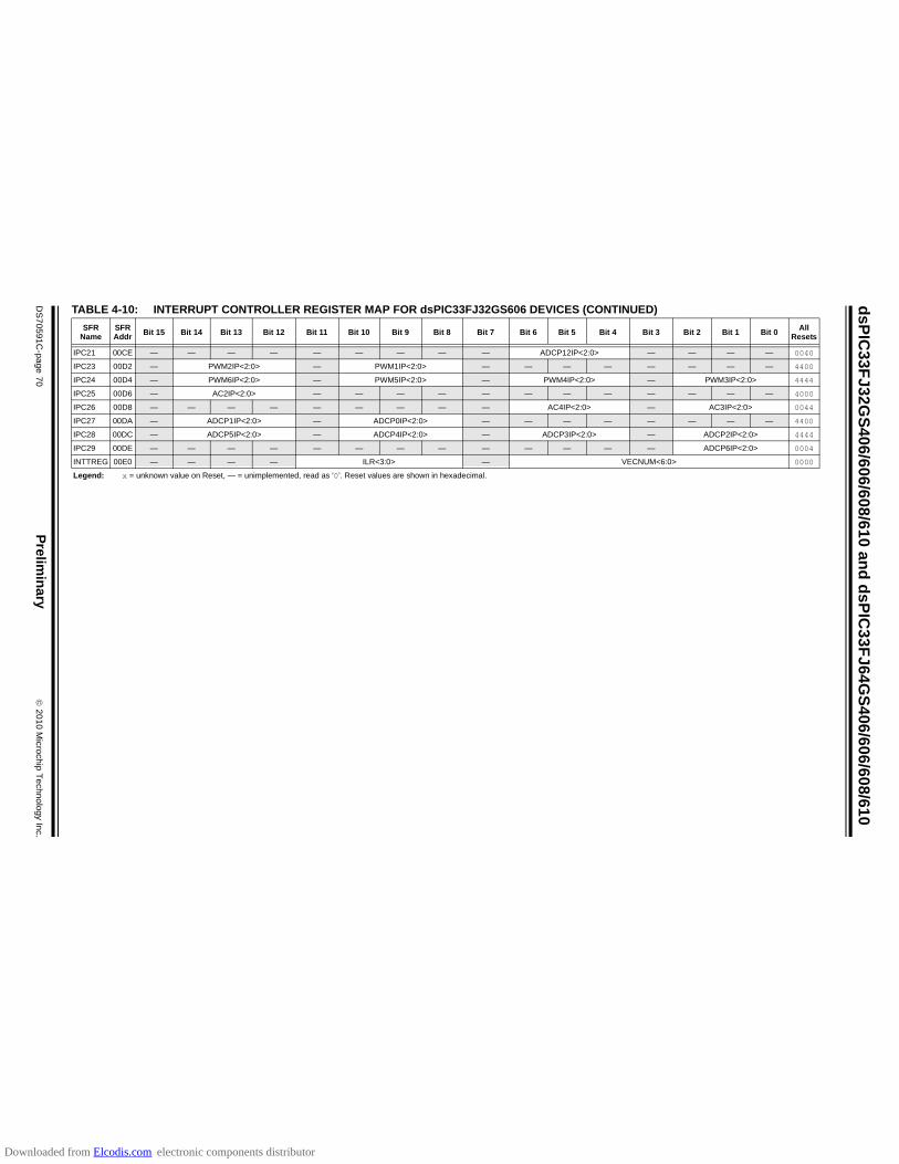
ds
PIC
33
FJ
32
GS
40
6/6
06
/60
8/6
10
an
d d
sP
IC3
3F
J6
4G
S4
06
/60
6/6
08/6
10
DS
70
59
1C
-pa
ge
70
Prelim
ina
ry
20
10
Micro
chip
Te
chn
olo
gy In
c.
IPC21 00CE — — — — — — — — — ADCP12IP<2:0> — — — — 0040
IPC23 00D2 — PWM2IP<2:0> — PWM1IP<2:0> — — — — — — — — 4400
IPC24 00D4 — PWM6IP<2:0> — PWM5IP<2:0> — PWM4IP<2:0> — PWM3IP<2:0> 4444
IPC25 00D6 — AC2IP<2:0> — — — — — — — — — — — — 4000
IPC26 00D8 — — — — — — — — — AC4IP<2:0> — AC3IP<2:0> 0044
IPC27 00DA — ADCP1IP<2:0> — ADCP0IP<2:0> — — — — — — — — 4400
IPC28 00DC — ADCP5IP<2:0> — ADCP4IP<2:0> — ADCP3IP<2:0> — ADCP2IP<2:0> 4444
IPC29 00DE — — — — — — — — — — — — — ADCP6IP<2:0> 0004
INTTREG 00E0 — — — — ILR<3:0> — VECNUM<6:0> 0000
TABLE 4-10: INTERRUPT CONTROLLER REGISTER MAP FOR dsPIC33FJ32GS606 DEVICES (CONTINUED)
SFR Name
SFR Addr
Bit 15 Bit 14 Bit 13 Bit 12 Bit 11 Bit 10 Bit 9 Bit 8 Bit 7 Bit 6 Bit 5 Bit 4 Bit 3 Bit 2 Bit 1 Bit 0All
Resets
Legend: x = unknown value on Reset, — = unimplemented, read as ‘0’. Reset values are shown in hexadecimal.
Downloaded from Elcodis.com electronic components distributor

2
01
0 M
icroch
ip T
ech
no
log
y Inc.
Prelim
inary
DS
70
59
1C
-pa
ge
71
ds
PIC
33
FJ
32
GS
40
6/6
06/6
08/6
10 a
nd
ds
PIC
33
FJ
64G
S4
06/6
06/60
8/61
0
TABLE 4-11: TIMERS REGISTER MAP
TABLE 4-12: INPUT CAPTURE REGISTER MAP
SFR Name
SFR Addr
Bit 15 Bit 14 Bit 13 Bit 12 Bit 11 Bit 10 Bit 9 Bit 8 Bit 7 Bit 6 Bit 5 Bit 4 Bit 3 Bit 2 Bit 1 Bit 0All
Resets
TMR1 0100 Timer1 Register xxxx
PR1 0102 Period Register 1 FFFF
T1CON 0104 TON — TSIDL — — — — — — TGATE TCKPS<1:0> — TSYNC TCS — 0000
TMR2 0106 Timer2 Register xxxx
TMR3HLD 0108 Timer3 Holding Register (for 32-bit timer operations only) xxxx
TMR3 010A Timer3 Register xxxx
PR2 010C Period Register 2 FFFF
PR3 010E Period Register 3 FFFF
T2CON 0110 TON — TSIDL — — — — — — TGATE TCKPS<1:0> T32 — TCS — 0000
T3CON 0112 TON — TSIDL — — — — — — TGATE TCKPS<1:0> — — TCS — 0000
TMR4 0114 Timer4 Register xxxx
TMR5HLD 0116 Timer5 Holding Register (for 32-bit timer operations only) xxxx
TMR5 0118 Timer5 Register xxxx
PR4 011A Period Register 4 FFFF
PR5 011C Period Register 5 FFFF
T4CON 011E TON — TSIDL — — — — — — TGATE TCKPS<1:0> T32 — TCS — 0000
T5CON 0120 TON — TSIDL — — — — — — TGATE TCKPS<1:0> — — TCS — 0000
Legend: x = unknown value on Reset, — = unimplemented, read as ‘0’. Reset values are shown in hexadecimal.
SFR Name
SFR Addr Bit 15 Bit 14 Bit 13 Bit 12 Bit 11 Bit 10 Bit 9 Bit 8 Bit 7 Bit 6 Bit 5 Bit 4 Bit 3 Bit 2 Bit 1 Bit 0All
Resets
IC1BUF 0140 Input 1 Capture Register xxxx
IC1CON 0142 — — ICSIDL — — — — — ICTMR ICI<1:0> ICOV ICBNE ICM<2:0> 0000
IC2BUF 0144 Input 2 Capture Register xxxx
IC2CON 0146 — — ICSIDL — — — — — ICTMR ICI<1:0> ICOV ICBNE ICM<2:0> 0000
IC3BUF 0148 Input 3 Capture Register xxxx
IC3CON 014A — — ICSIDL — — — — — ICTMR ICI<1:0> ICOV ICBNE ICM<2:0> 0000
IC4BUF 014C Input 4 Capture Register xxxx
IC4CON 014E — — ICSIDL — — — — — ICTMR ICI<1:0> ICOV ICBNE ICM<2:0> 0000
Legend: x = unknown value on Reset, — = unimplemented, read as ‘0’. Reset values are shown in hexadecimal.
Downloaded from Elcodis.com electronic components distributor

ds
PIC
33
FJ
32
GS
40
6/6
06
/60
8/6
10
an
d d
sP
IC3
3F
J6
4G
S4
06
/60
6/6
08/6
10
DS
70
59
1C
-pa
ge
72
Prelim
ina
ry
20
10
Micro
chip
Te
chn
olo
gy In
c.
TABLE 4-13: OUTPUT COMPARE REGISTER MAP
SFR Name
SFR Addr
Bit 15 Bit 14 Bit 13 Bit 12 Bit 11 Bit 10 Bit 9 Bit 8 Bit 7 Bit 6 Bit 5 Bit 4 Bit 3 Bit 2 Bit 1 Bit 0All
Resets
OC1RS 0180 Output Compare 1 Secondary Register xxxx
OC1R 0182 Output Compare 1 Register xxxx
OC1CON 0184 — — OCSIDL — — — — — — — — OCFLT OCTSEL OCM<2:0> 0000
OC2RS 0186 Output Compare 2 Secondary Register xxxx
OC2R 0188 Output Compare 2 Register xxxx
OC2CON 018A — — OCSIDL — — — — — — — — OCFLT OCTSEL OCM<2:0> 0000
OC3RS 018C Output Compare 3 Secondary Register xxxx
OC3R 018E Output Compare 3 Register xxxx
OC3CON 0190 — — OCSIDL — — — — — — — — OCFLT OCTSEL OCM<2:0> 0000
OC4RS 0192 Output Compare 4 Secondary Register xxxx
OC4R 0194 Output Compare 4 Register xxxx
OC4CON 0196 — — OCSIDL — — — — — — — — OCFLT OCTSEL OCM<2:0> 0000
Legend: x = unknown value on Reset, — = unimplemented, read as ‘0’. Reset values are shown in hexadecimal.
TABLE 4-14: QEI1 REGISTER MAP
SFR Name
Addr. Bit 15 Bit 14 Bit 13 Bit 12 Bit 11 Bit 10 Bit 9 Bit 8 Bit 7 Bit 6 Bit 5 Bit 4 Bit 3 Bit 2 Bit 1 Bit 0All
Resets
QEI1CON 01E0 CNTERR — QEISIDL INDX UPDN QEIM<2:0> SWPAB PCDOUT TQGATE TQCKPS<1:0> POSRES TQCS UPDN_SRC 0000
DFLT1CON 01E2 — — — — — IMV<1:0> CEID QEOUT QECK<2:0> — — — — 0000
POS1CNT 01E4 Position Counter<15:0> 0000
MAX1CNT 01E6 Maximum Count<15:0> FFFF
Legend: u = uninitialized bit, — = unimplemented, read as ‘0’
TABLE 4-15: QEI2 REGISTER MAP
SFR Name
Addr. Bit 15 Bit 14 Bit 13 Bit 12 Bit 11 Bit 10 Bit 9 Bit 8 Bit 7 Bit 6 Bit 5 Bit 4 Bit 3 Bit 2 Bit 1 Bit 0All
Resets
QEI2CON 01F0 CNTERR — QEISIDL INDX UPDN QEIM<2:0> SWPAB PCDOUT TQGATE TQCKPS<1:0> POSRES TQCS UPDN_SRC 0000
DFLT2CON 01F2 — — — — — IMV<1:0> CEID QEOUT QECK<2:0> — — — — 0000
POS2CNT 01F4 Position Counter<15:0> 0000
MAX2CNT 01F6 Maximum Count<15:0> FFFF
Legend: u = uninitialized bit, — = unimplemented, read as ‘0’
Downloaded from Elcodis.com electronic components distributor

2
01
0 M
icroch
ip T
ech
no
log
y Inc.
Prelim
inary
DS
70
59
1C
-pa
ge
73
ds
PIC
33
FJ
32
GS
40
6/6
06/6
08/6
10 a
nd
ds
PIC
33
FJ
64G
S4
06/6
06/60
8/61
0
TABLE 4-16: HIGH-SPEED PWM REGISTER MAP
File NameAddr Offset
Bit 15 Bit 14 Bit 13 Bit 12 Bit 11 Bit 10 Bit 9 Bit 8 Bit 7 Bit 6 Bit 5 Bit 4 Bit 3 Bit 2 Bit 1 Bit 0All
Resets
PTCON 0400 PTEN — PTSIDL SESTAT SEIEN EIPU SYNCPOL SYNCOEN SYNCEN SYNCSRC<2:0> SEVTPS<3:0> 0000
PTCON2 0402 — — — — — — — — — — — — — PCLKDIV<2:0> 0000
PTPER 0404 PTPER<15:0> FFF8
SEVTCMP 0406 SEVTCMP<15:3> — — — 0000
MDC 040A MDC<15:0> 0000
STCON 040E — — — SESTAT SEIEN EIPU SYNCPOL SYNCOEN SYNCEN SYNCSRC<2:0> SEVTPS<3:0> 0000
STCON2 0410 — — — — — — — — — — — — — PCLKDIV<2:0> 0000
STPER 0412 PTPER<15:0> FFF8
SSEVTCMP 0414 SSEVTCMP<15:3> — — — 0000
CHOP 041A CHPCLKEN — — — — — CHOP<9:3> — — — 0000
Legend: x = unknown value on Reset, — = unimplemented, read as ‘0’. Reset values are shown in hexadecimal.
TABLE 4-17: HIGH-SPEED PWM GENERATOR 1 REGISTER MAP
File NameAddr Offset
Bit 15 Bit 14 Bit 13 Bit 12 Bit 11 Bit 10 Bit 9 Bit 8 Bit 7 Bit 6 Bit 5 Bit 4 Bit 3 Bit 2 Bit 1 Bit 0All
Resets
PWMCON1 0420 FLTSTAT CLSTAT TRGSTAT FLTIEN CLIEN TRGIEN ITB MDCS DTC<1:0> DTCP — MTBS CAM XPRES IUE 0000
IOCON1 0422 PENH PENL POLH POLL PMOD<1:0> OVRENH OVRENL OVRDAT<1:0> FLTDAT<1:0> CLDAT<1:0> SWAP OSYNC 0000
FCLCON1 0424 IFLTMOD CLSRC<4:0> CLPOL CLMOD FLTSRC<4:0> FLTPOL FLTMOD<1:0> 0000
PDC1 0426 PDC1<15:0> 0000
PHASE1 0428 PHASE1<15:0> 0000
DTR1 042A — — DTR1<13:0> 0000
ALTDTR1 042C — — ALTDTR1<13:0> 0000
SDC1 042E SDC1<15:0> 0000
SPHASE1 0430 SPHASE1<15:0> 0000
TRIG1 0432 TRGCMP<15:3> — — — 0000
TRGCON1 0434 TRGDIV<3:0> — — — — DTM — TRGSTRT<5:0> 0000
STRIG1 0436 STRGCMP<15:3> — — — 0000
PWMCAP1 0438 PWMCAP1<15:3> — — — 0000
LEBCON1 043A PHR PHF PLR PLF FLTLEBEN CLLEBEN — — — — BCH BCL BPHH BPHL BPLH BPLL 0000
LEBDLY1 043C — — — — LEB<11:3> — — — 0000
AUXCON1 043E HRPDIS HRDDIS — — BLANKSEL<3:0> — — CHOPSEL<3:0> CHOPHEN CHOPLEN 0000
Legend: x = unknown value on Reset, — = unimplemented, read as ‘0’. Reset values are shown in hexadecimal.
Downloaded from Elcodis.com electronic components distributor
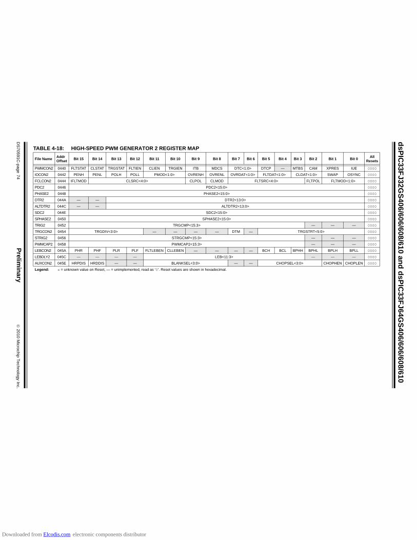
ds
PIC
33
FJ
32
GS
40
6/6
06
/60
8/6
10
an
d d
sP
IC3
3F
J6
4G
S4
06
/60
6/6
08/6
10
DS
70
59
1C
-pa
ge
74
Prelim
ina
ry
20
10
Micro
chip
Te
chn
olo
gy In
c.
TABLE 4-18: HIGH-SPEED PWM GENERATOR 2 REGISTER MAP
File NameAddr Offset
Bit 15 Bit 14 Bit 13 Bit 12 Bit 11 Bit 10 Bit 9 Bit 8 Bit 7 Bit 6 Bit 5 Bit 4 Bit 3 Bit 2 Bit 1 Bit 0All
Resets
PWMCON2 0440 FLTSTAT CLSTAT TRGSTAT FLTIEN CLIEN TRGIEN ITB MDCS DTC<1:0> DTCP — MTBS CAM XPRES IUE 0000
IOCON2 0442 PENH PENL POLH POLL PMOD<1:0> OVRENH OVRENL OVRDAT<1:0> FLTDAT<1:0> CLDAT<1:0> SWAP OSYNC 0000
FCLCON2 0444 IFLTMOD CLSRC<4:0> CLPOL CLMOD FLTSRC<4:0> FLTPOL FLTMOD<1:0> 0000
PDC2 0446 PDC2<15:0> 0000
PHASE2 0448 PHASE2<15:0> 0000
DTR2 044A — — DTR2<13:0> 0000
ALTDTR2 044C — — ALTDTR2<13:0> 0000
SDC2 044E SDC2<15:0> 0000
SPHASE2 0450 SPHASE2<15:0> 0000
TRIG2 0452 TRGCMP<15:3> — — — 0000
TRGCON2 0454 TRGDIV<3:0> — — — — DTM — TRGSTRT<5:0> 0000
STRIG2 0456 STRGCMP<15:3> — — — 0000
PWMCAP2 0458 PWMCAP2<15:3> — — — 0000
LEBCON2 045A PHR PHF PLR PLF FLTLEBEN CLLEBEN — — — — BCH BCL BPHH BPHL BPLH BPLL 0000
LEBDLY2 045C — — — — LEB<11:3> — — — 0000
AUXCON2 045E HRPDIS HRDDIS — — BLANKSEL<3:0> — — CHOPSEL<3:0> CHOPHEN CHOPLEN 0000
Legend: x = unknown value on Reset, — = unimplemented, read as ‘0’. Reset values are shown in hexadecimal.
Downloaded from Elcodis.com electronic components distributor

2
01
0 M
icroch
ip T
ech
no
log
y Inc.
Prelim
inary
DS
70
59
1C
-pa
ge
75
ds
PIC
33
FJ
32
GS
40
6/6
06/6
08/6
10 a
nd
ds
PIC
33
FJ
64G
S4
06/6
06/60
8/61
0
TABLE 4-19: HIGH-SPEED PWM GENERATOR 3 REGISTER MAP
File NameAddr Offset
Bit 15 Bit 14 Bit 13 Bit 12 Bit 11 Bit 10 Bit 9 Bit 8 Bit 7 Bit 6 Bit 5 Bit 4 Bit 3 Bit 2 Bit 1 Bit 0All
Resets
PWMCON3 0460 FLTSTAT CLSTAT TRGSTAT FLTIEN CLIEN TRGIEN ITB MDCS DTC<1:0> DTCP — MTBS CAM XPRES IUE 0000
IOCON3 0462 PENH PENL POLH POLL PMOD<1:0> OVRENH OVRENL OVRDAT<1:0> FLTDAT<1:0> CLDAT<1:0> SWAP OSYNC 0000
FCLCON3 0464 IFLTMOD CLSRC<4:0> CLPOL CLMOD FLTSRC<4:0> FLTPOL FLTMOD<1:0> 0000
PDC3 0466 PDC3<15:0> 0000
PHASE3 0468 PHASE3<15:0> 0000
DTR3 046C — — DTR3<13:0> 0000
ALTDTR3 046C — — ALTDTR3<13:0> 0000
SDC3 046E SDC3<15:0> 0000
SPHASE3 0470 SPHASE3<15:0> 0000
TRIG3 0472 TRGCMP<15:3> — — — 0000
TRGCON3 0474 TRGDIV<3:0> — — — — DTM — TRGSTRT<5:0> 0000
STRIG3 0476 STRGCMP<15:3> — — — 0000
PWMCAP3 0478 PWMCAP3<15:3> — — — 0000
LEBCON3 047A PHR PHF PLR PLF FLTLEBEN CLLEBEN — — — — BCH BCL BPHH BPHL BPLH BPLL 0000
LEBDLY3 047C — — — — LEB<11:3> — — — 0000
AUXCON3 047E HRPDIS HRDDIS — — BLANKSEL<3:0> — — CHOPSEL<3:0> CHOPHEN CHOPLEN 0000
Legend: x = unknown value on Reset, — = unimplemented, read as ‘0’. Reset values are shown in hexadecimal.
Downloaded from Elcodis.com electronic components distributor

ds
PIC
33
FJ
32
GS
40
6/6
06
/60
8/6
10
an
d d
sP
IC3
3F
J6
4G
S4
06
/60
6/6
08/6
10
DS
70
59
1C
-pa
ge
76
Prelim
ina
ry
20
10
Micro
chip
Te
chn
olo
gy In
c.
TABLE 4-20: HIGH-SPEED PWM GENERATOR 4 REGISTER MAP
File NameAddr Offset
Bit 15 Bit 14 Bit 13 Bit 12 Bit 11 Bit 10 Bit 9 Bit 8 Bit 7 Bit 6 Bit 5 Bit 4 Bit 3 Bit 2 Bit 1 Bit 0All
Resets
PWMCON4 0480 FLTSTAT CLSTAT TRGSTAT FLTIEN CLIEN TRGIEN ITB MDCS DTC<1:0> DTCP — MTBS CAM XPRES IUE 0000
IOCON4 0482 PENH PENL POLH POLL PMOD<1:0> OVRENH OVRENL OVRDAT<1:0> FLTDAT<1:0> CLDAT<1:0> SWAP OSYNC 0000
FCLCON4 0484 IFLTMOD CLSRC<4:0> CLPOL CLMOD FLTSRC<4:0> FLTPOL FLTMOD<1:0> 0000
PDC4 0486 PDC4<15:0> 0000
PHASE4 0488 PHASE4<15:0> 0000
DTR4 048A — — DTR4<13:0> 0000
ALTDTR4 048A — — ALTDTR4<13:0> 0000
SDC4 048E SDC4<15:0> 0000
SPHASE4 0490 SPHASE4<15:0> 0000
TRIG4 0492 TRGCMP<15:3> — — — 0000
TRGCON4 0494 TRGDIV<3:0> — — — — DTM — TRGSTRT<5:0> 0000
STRIG4 0496 STRGCMP<15:3> — — — 0000
PWMCAP4 0498 PWMCAP4<15:3> — — — 0000
LEBCON4 049A PHR PHF PLR PLF FLTLEBEN CLLEBEN — — — — BCH BCL BPHH BPHL BPLH BPLL 0000
LEBDLY4 049C — — — — LEB<11:3> — — — 0000
AUXCON4 049E HRPDIS HRDDIS — — BLANKSEL<3:0> — — CHOPSEL<3:0> CHOPHEN CHOPLEN 0000
Legend: x = unknown value on Reset, — = unimplemented, read as ‘0’. Reset values are shown in hexadecimal.
Downloaded from Elcodis.com electronic components distributor
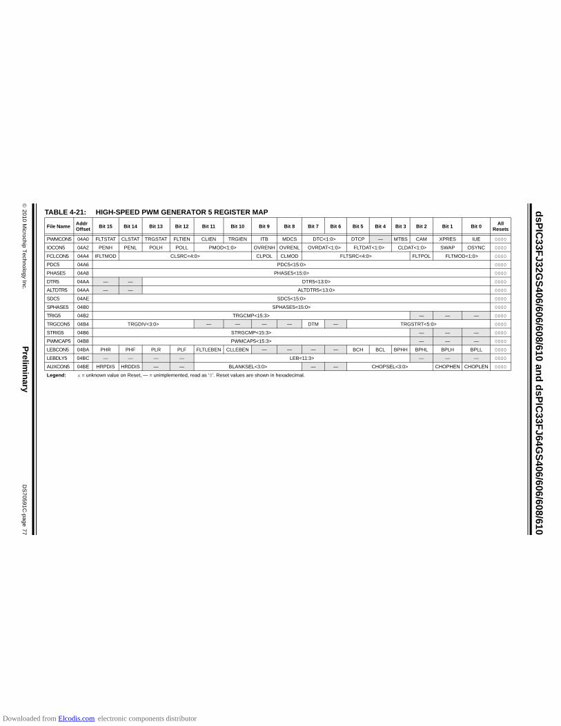
2
01
0 M
icroch
ip T
ech
no
log
y Inc.
Prelim
inary
DS
70
59
1C
-pa
ge
77
ds
PIC
33
FJ
32
GS
40
6/6
06/6
08/6
10 a
nd
ds
PIC
33
FJ
64G
S4
06/6
06/60
8/61
0
TABLE 4-21: HIGH-SPEED PWM GENERATOR 5 REGISTER MAP
File NameAddr Offset
Bit 15 Bit 14 Bit 13 Bit 12 Bit 11 Bit 10 Bit 9 Bit 8 Bit 7 Bit 6 Bit 5 Bit 4 Bit 3 Bit 2 Bit 1 Bit 0All
Resets
PWMCON5 04A0 FLTSTAT CLSTAT TRGSTAT FLTIEN CLIEN TRGIEN ITB MDCS DTC<1:0> DTCP — MTBS CAM XPRES IUE 0000
IOCON5 04A2 PENH PENL POLH POLL PMOD<1:0> OVRENH OVRENL OVRDAT<1:0> FLTDAT<1:0> CLDAT<1:0> SWAP OSYNC 0000
FCLCON5 04A4 IFLTMOD CLSRC<4:0> CLPOL CLMOD FLTSRC<4:0> FLTPOL FLTMOD<1:0> 0000
PDC5 04A6 PDC5<15:0> 0000
PHASE5 04A8 PHASE5<15:0> 0000
DTR5 04AA — — DTR5<13:0> 0000
ALTDTR5 04AA — — ALTDTR5<13:0> 0000
SDC5 04AE SDC5<15:0> 0000
SPHASE5 04B0 SPHASE5<15:0> 0000
TRIG5 04B2 TRGCMP<15:3> — — — 0000
TRGCON5 04B4 TRGDIV<3:0> — — — — DTM — TRGSTRT<5:0> 0000
STRIG5 04B6 STRGCMP<15:3> — — — 0000
PWMCAP5 04B8 PWMCAP5<15:3> — — — 0000
LEBCON5 04BA PHR PHF PLR PLF FLTLEBEN CLLEBEN — — — — BCH BCL BPHH BPHL BPLH BPLL 0000
LEBDLY5 04BC — — — — LEB<11:3> — — — 0000
AUXCON5 04BE HRPDIS HRDDIS — — BLANKSEL<3:0> — — CHOPSEL<3:0> CHOPHEN CHOPLEN 0000
Legend: x = unknown value on Reset, — = unimplemented, read as ‘0’. Reset values are shown in hexadecimal.
Downloaded from Elcodis.com electronic components distributor

ds
PIC
33
FJ
32
GS
40
6/6
06
/60
8/6
10
an
d d
sP
IC3
3F
J6
4G
S4
06
/60
6/6
08/6
10
DS
70
59
1C
-pa
ge
78
Prelim
ina
ry
20
10
Micro
chip
Te
chn
olo
gy In
c.
TABLE 4-22: HIGH-SPEED PWM GENERATOR 6 REGISTER MAP
File NameAddr Offset
Bit 15 Bit 14 Bit 13 Bit 12 Bit 11 Bit 10 Bit 9 Bit 8 Bit 7 Bit 6 Bit 5 Bit 4 Bit 3 Bit 2 Bit 1 Bit 0All
Resets
PWMCON6 04C0 FLTSTAT CLSTAT TRGSTAT FLTIEN CLIEN TRGIEN ITB MDCS DTC<1:0> DTCP — MTBS CAM XPRES IUE 0000
IOCON6 04C2 PENH PENL POLH POLL PMOD<1:0> OVRENH OVRENL OVRDAT<1:0> FLTDAT<1:0> CLDAT<1:0> SWAP OSYNC 0000
FCLCON6 04C4 IFLTMOD CLSRC<4:0> CLPOL CLMOD FLTSRC<4:0> FLTPOL FLTMOD<1:0> 0000
PDC6 04C6 PDC6<15:0> 0000
PHASE6 04C8 PHASE6<15:0> 0000
DTR6 04CA — — DTR6<13:0> 0000
ALTDTR6 04CA — — ALTDTR6<13:0> 0000
SDC6 04CE SDC6<15:0> 0000
SPHASE6 04D0 SPHASE6<15:0> 0000
TRIG6 04D2 TRGCMP<15:3> — — — 0000
TRGCON6 04D4 TRGDIV<3:0> — — — — DTM — TRGSTRT<5:0> 0000
STRIG6 04D6 STRGCMP<15:3> — — — 0000
PWMCAP6 04D8 PWMCAP6<15:3> — — — 0000
LEBCON6 04DA PHR PHF PLR PLF FLTLEBEN CLLEBEN — — — — BCH BCL BPHH BPHL BPLH BPLL 0000
LEBDLY6 04DC — — — — LEB<11:3> — — — 0000
AUXCON6 04DE HRPDIS HRDDIS — — BLANKSEL<3:0> — — CHOPSEL<3:0> CHOPHEN CHOPLEN 0000
Legend: x = unknown value on Reset, — = unimplemented, read as ‘0’. Reset values are shown in hexadecimal.
Downloaded from Elcodis.com electronic components distributor

2
01
0 M
icroch
ip T
ech
no
log
y Inc.
Prelim
inary
DS
70
59
1C
-pa
ge
79
ds
PIC
33
FJ
32
GS
40
6/6
06/6
08/6
10 a
nd
ds
PIC
33
FJ
64G
S4
06/6
06/60
8/61
0
TABLE 4-23: HIGH-SPEED PWM GENERATOR 7 REGISTER MAP (EXCLUDES dsPIC33FJ32GS406 AND dsPIC33FJ64GS406 DEVICES)
File NameAddr Offset
Bit 15 Bit 14 Bit 13 Bit 12 Bit 11 Bit 10 Bit 9 Bit 8 Bit 7 Bit 6 Bit 5 Bit 4 Bit 3 Bit 2 Bit 1 Bit 0All
Resets
PWMCON7 04E0 FLTSTAT CLSTAT TRGSTAT FLTIEN CLIEN TRGIEN ITB MDCS DTC<1:0> DTCP — MTBS CAM XPRES IUE 0000
IOCON7 04E2 PENH PENL POLH POLL PMOD<1:0> OVRENH OVRENL OVRDAT<1:0> FLTDAT<1:0> CLDAT<1:0> SWAP OSYNC 0000
FCLCON7 04E4 IFLTMOD CLSRC<4:0> CLPOL CLMOD FLTSRC<4:0> FLTPOL FLTMOD<1:0> 0000
PDC7 04E6 PDC7<15:0> 0000
PHASE7 04E8 PHASE7<15:0> 0000
DTR7 04EA — — DTR7<13:0> 0000
ALTDTR7 04EA — — ALTDTR7<13:0> 0000
SDC7 04EE SDC7<15:0> 0000
SPHASE7 04F0 SPHASE7<15:0> 0000
TRIG7 04F2 TRGCMP<15:3> — — — 0000
TRGCON7 04F4 TRGDIV<3:0> — — — — DTM — TRGSTRT<5:0> 0000
STRIG7 04F6 STRGCMP<15:3> — — — 0000
PWMCAP7 04F8 PWMCAP7<15:3> — — — 0000
LEBCON7 04FA PHR PHF PLR PLF FLTLEBEN CLLEBEN — — — — BCH BCL BPHH BPHL BPLH BPLL 0000
LEBDLY7 04FC — — — — LEB<11:3> — — — 0000
AUXCON7 04FE HRPDIS HRDDIS — — BLANKSEL<3:0> — — CHOPSEL<3:0> CHOPHEN CHOPLEN 0000
Legend: x = unknown value on Reset, — = unimplemented, read as ‘0’. Reset values are shown in hexadecimal.
Downloaded from Elcodis.com electronic components distributor
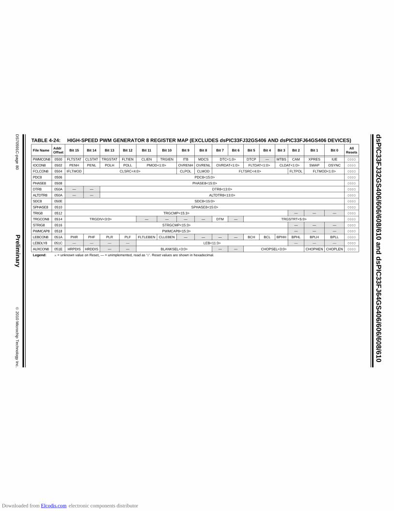
ds
PIC
33
FJ
32
GS
40
6/6
06
/60
8/6
10
an
d d
sP
IC3
3F
J6
4G
S4
06
/60
6/6
08/6
10
DS
70
59
1C
-pa
ge
80
Prelim
ina
ry
20
10
Micro
chip
Te
chn
olo
gy In
c.
TABLE 4-24: HIGH-SPEED PWM GENERATOR 8 REGISTER MAP (EXCLUDES dsPIC33FJ32GS406 AND dsPIC33FJ64GS406 DEVICES)
File NameAddr Offset
Bit 15 Bit 14 Bit 13 Bit 12 Bit 11 Bit 10 Bit 9 Bit 8 Bit 7 Bit 6 Bit 5 Bit 4 Bit 3 Bit 2 Bit 1 Bit 0All
Resets
PWMCON8 0500 FLTSTAT CLSTAT TRGSTAT FLTIEN CLIEN TRGIEN ITB MDCS DTC<1:0> DTCP — MTBS CAM XPRES IUE 0000
IOCON8 0502 PENH PENL POLH POLL PMOD<1:0> OVRENH OVRENL OVRDAT<1:0> FLTDAT<1:0> CLDAT<1:0> SWAP OSYNC 0000
FCLCON8 0504 IFLTMOD CLSRC<4:0> CLPOL CLMOD FLTSRC<4:0> FLTPOL FLTMOD<1:0> 0000
PDC8 0506 PDC8<15:0> 0000
PHASE8 0508 PHASE8<15:0> 0000
DTR8 050A — — DTR8<13:0> 0000
ALTDTR8 050A — — ALTDTR8<13:0> 0000
SDC8 050E SDC8<15:0> 0000
SPHASE8 0510 SPHASE8<15:0> 0000
TRIG8 0512 TRGCMP<15:3> — — — 0000
TRGCON8 0514 TRGDIV<3:0> — — — — DTM — TRGSTRT<5:0> 0000
STRIG8 0516 STRGCMP<15:3> — — — 0000
PWMCAP8 0518 PWMCAP8<15:3> — — — 0000
LEBCON8 051A PHR PHF PLR PLF FLTLEBEN CLLEBEN — — — — BCH BCL BPHH BPHL BPLH BPLL 0000
LEBDLY8 051C — — — — LEB<11:3> — — — 0000
AUXCON8 051E HRPDIS HRDDIS — — BLANKSEL<3:0> — — CHOPSEL<3:0> CHOPHEN CHOPLEN 0000
Legend: x = unknown value on Reset, — = unimplemented, read as ‘0’. Reset values are shown in hexadecimal.
Downloaded from Elcodis.com electronic components distributor
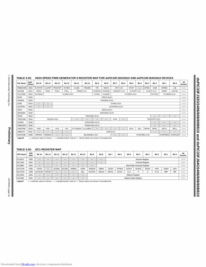
2
01
0 M
icroch
ip T
ech
no
log
y Inc.
Prelim
inary
DS
70
59
1C
-pa
ge
81
ds
PIC
33
FJ
32
GS
40
6/6
06/6
08/6
10 a
nd
ds
PIC
33
FJ
64G
S4
06/6
06/60
8/61
0
TABLE 4-25: HIGH-SPEED PWM GENERATOR 9 REGISTER MAP FOR dsPIC33FJ32GS610 AND dsPIC33FJ64GS610 DEVICES
File NameAddr Offset
Bit 15 Bit 14 Bit 13 Bit 12 Bit 11 Bit 10 Bit 9 Bit 8 Bit 7 Bit 6 Bit 5 Bit 4 Bit 3 Bit 2 Bit 1 Bit 0All
Resets
PWMCON9 0520 FLTSTAT CLSTAT TRGSTAT FLTIEN CLIEN TRGIEN ITB MDCS DTC<1:0> DTCP — MTBS CAM XPRES IUE 0000
IOCON9 0522 PENH PENL POLH POLL PMOD<1:0> OVRENH OVRENL OVRDAT<1:0> FLTDAT<1:0> CLDAT<1:0> SWAP OSYNC 0000
FCLCON9 0524 IFLTMOD CLSRC<4:0> CLPOL CLMOD FLTSRC<4:0> FLTPOL FLTMOD<1:0> 0000
PDC9 0526 PDC9<15:0> 0000
PHASE9 0528 PHASE9<15:0> 0000
DTR9 052A — — DTR9<13:0> 0000
ALTDTR9 052A — — ALTDTR9<13:0> 0000
SDC9 052E SDC9<15:0> 0000
SPHASE9 0530 SPHASE9<15:0> 0000
TRIG9 0532 TRGCMP<15:3> — — — 0000
TRGCON9 0534 TRGDIV<3:0> — — — — DTM — TRGSTRT<5:0> 0000
STRIG9 0536 STRGCMP<15:3> — — — 0000
PWMCAP9 0538 PWMCAP9<15:3> — — — 0000
LEBCON9 053A PHR PHF PLR PLF FLTLEBEN CLLEBEN — — — — BCH BCL BPHH BPHL BPLH BPLL 0000
LEBDLY9 053C — — — — LEB<11:3> — — — 0000
AUXCON9 053E HRPDIS HRDDIS — — BLANKSEL<3:0> — — CHOPSEL<3:0> CHOPHEN CHOPLEN 0000
Legend: x = unknown value on Reset, — = unimplemented, read as ‘0’. Reset values are shown in hexadecimal.
TABLE 4-26: I2C1 REGISTER MAP
SFR NameSFR Addr
Bit 15 Bit 14 Bit 13 Bit 12 Bit 11 Bit 10 Bit 9 Bit 8 Bit 7 Bit 6 Bit 5 Bit 4 Bit 3 Bit 2 Bit 1 Bit 0All
Resets
I2C1RCV 0200 — — — — — — — — Receive Register 0000
I2C1TRN 0202 — — — — — — — — Transmit Register 00FF
I2C1BRG 0204 — — — — — — — Baud Rate Generator Register 0000
I2C1CON 0206 I2CEN — I2CSIDL SCLREL IPMIEN A10M DISSLW SMEN GCEN STREN ACKDT ACKEN RCEN PEN RSEN SEN 1000
I2C1STAT 0208 ACKSTAT TRSTAT — — — BCL GCSTAT ADD10 IWCOL I2COV D_A P S R_W RBF TBF 0000
I2C1ADD 020A — — — — — — Address Register 0000
I2C1MSK 020C — — — — — — Address Mask Register 0000
Legend: x = unknown value on Reset, — = unimplemented, read as ‘0’. Reset values are shown in hexadecimal.
Downloaded from Elcodis.com electronic components distributor

ds
PIC
33
FJ
32
GS
40
6/6
06
/60
8/6
10
an
d d
sP
IC3
3F
J6
4G
S4
06
/60
6/6
08/6
10
DS
70
59
1C
-pa
ge
82
Prelim
ina
ry
20
10
Micro
chip
Te
chn
olo
gy In
c.
TABLE 4-28: UART1 REGISTER MAP
TABLE 4-27: I2C2 REGISTER MAP
SFR NameSFR Addr
Bit 15 Bit 14 Bit 13 Bit 12 Bit 11 Bit 10 Bit 9 Bit 8 Bit 7 Bit 6 Bit 5 Bit 4 Bit 3 Bit 2 Bit 1 Bit 0All
Resets
I2C2RCV 0210 — — — — — — — — Receive Register 0000
I2C2TRN 0212 — — — — — — — — Transmit Register 00FF
I2C2BRG 0214 — — — — — — — Baud Rate Generator Register 0000
I2C2CON 0216 I2CEN — I2CSIDL SCLREL IPMIEN A10M DISSLW SMEN GCEN STREN ACKDT ACKEN RCEN PEN RSEN SEN 1000
I2C2STAT 0218 ACKSTAT TRSTAT — — — BCL GCSTAT ADD10 IWCOL I2COV D_A P S R_W RBF TBF 0000
I2C2ADD 021A — — — — — — Address Register 0000
I2C2MSK 021C — — — — — — Address Mask Register 0000
Legend: x = unknown value on Reset, — = unimplemented, read as ‘0’. Reset values are shown in hexadecimal.
SFR NameSFR Addr
Bit 15 Bit 14 Bit 13 Bit 12 Bit 11 Bit 10 Bit 9 Bit 8 Bit 7 Bit 6 Bit 5 Bit 4 Bit 3 Bit 2 Bit 1 Bit 0All
Resets
U1MODE 0220 UARTEN — USIDL IREN RTSMD — UEN1 UEN0 WAKE LPBACK ABAUD URXINV BRGH PDSEL<1:0> STSEL 0000
U1STA 0222 UTXISEL1 UTXINV UTXISEL0 — UTXBRK UTXEN UTXBF TRMT URXISEL<1:0> ADDEN RIDLE PERR FERR OERR URXDA 0110
U1TXREG 0224 — — — — — — — UART Transmit Register xxxx
U1RXREG 0226 — — — — — — — UART Receive Register 0000
U1BRG 0228 Baud Rate Generator Prescaler 0000
Legend: x = unknown value on Reset, — = unimplemented, read as ‘0’. Reset values are shown in hexadecimal.
TABLE 4-29: UART2 REGISTER MAP
SFR Name
SFR Addr
Bit 15 Bit 14 Bit 13 Bit 12 Bit 11 Bit 10 Bit 9 Bit 8 Bit 7 Bit 6 Bit 5 Bit 4 Bit 3 Bit 2 Bit 1 Bit 0All
Resets
U2MODE 0230 UARTEN — USIDL IREN RTSMD — UEN1 UEN0 WAKE LPBACK ABAUD URXINV BRGH PDSEL<1:0> STSEL 0000
U2STA 0232 UTXISEL1 UTXINV UTXISEL0 — UTXBRK UTXEN UTXBF TRMT URXISEL<1:0> ADDEN RIDLE PERR FERR OERR URXDA 0110
U2TXREG 0234 — — — — — — — UART Transmit Register xxxx
U2RXREG 0236 — — — — — — — UART Receive Register 0000
U2BRG 0238 Baud Rate Generator Prescaler 0000
Legend: x = unknown value on Reset, — = unimplemented, read as ‘0’. Reset values are shown in hexadecimal.
Downloaded from Elcodis.com electronic components distributor
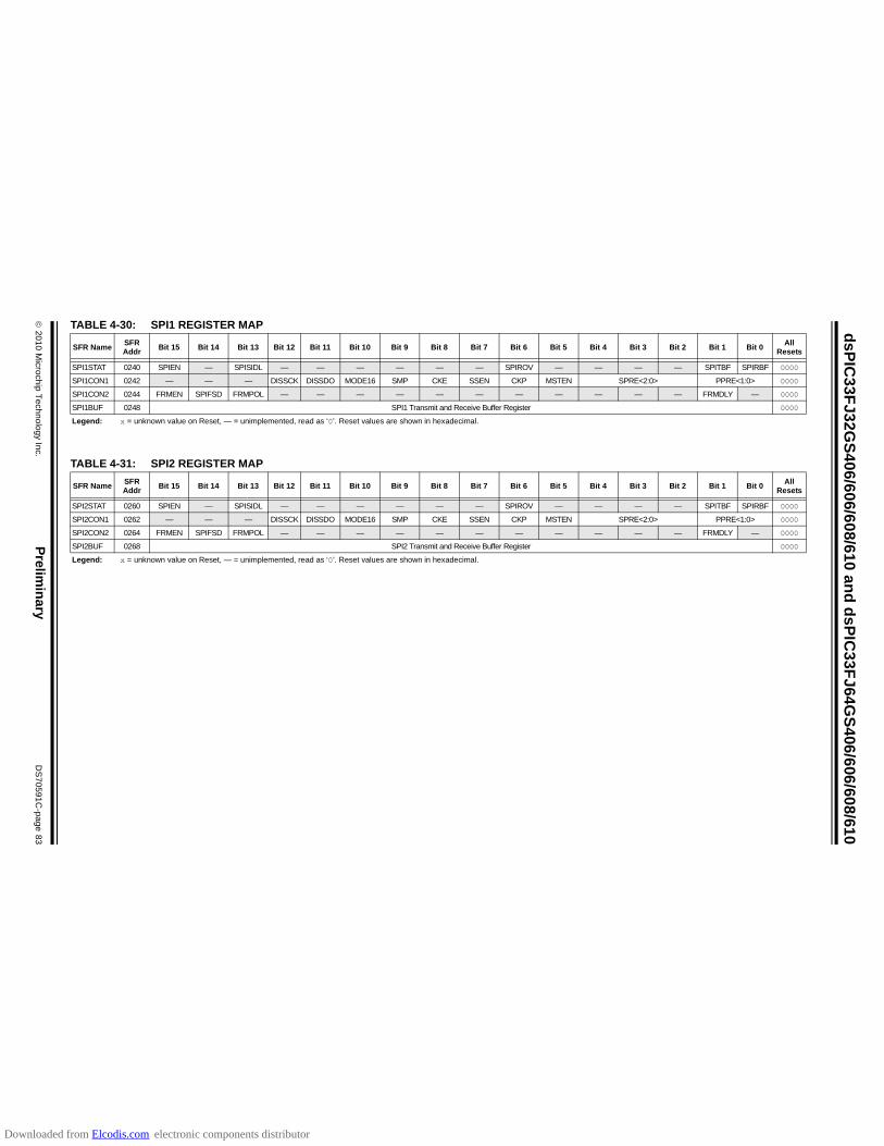
2
01
0 M
icroch
ip T
ech
no
log
y Inc.
Prelim
inary
DS
70
59
1C
-pa
ge
83
ds
PIC
33
FJ
32
GS
40
6/6
06/6
08/6
10 a
nd
ds
PIC
33
FJ
64G
S4
06/6
06/60
8/61
0
TABLE 4-30: SPI1 REGISTER MAP
TABLE 4-31: SPI2 REGISTER MAP
SFR NameSFR Addr
Bit 15 Bit 14 Bit 13 Bit 12 Bit 11 Bit 10 Bit 9 Bit 8 Bit 7 Bit 6 Bit 5 Bit 4 Bit 3 Bit 2 Bit 1 Bit 0All
Resets
SPI1STAT 0240 SPIEN — SPISIDL — — — — — — SPIROV — — — — SPITBF SPIRBF 0000
SPI1CON1 0242 — — — DISSCK DISSDO MODE16 SMP CKE SSEN CKP MSTEN SPRE<2:0> PPRE<1:0> 0000
SPI1CON2 0244 FRMEN SPIFSD FRMPOL — — — — — — — — — — — FRMDLY — 0000
SPI1BUF 0248 SPI1 Transmit and Receive Buffer Register 0000
Legend: x = unknown value on Reset, — = unimplemented, read as ‘0’. Reset values are shown in hexadecimal.
SFR NameSFR Addr
Bit 15 Bit 14 Bit 13 Bit 12 Bit 11 Bit 10 Bit 9 Bit 8 Bit 7 Bit 6 Bit 5 Bit 4 Bit 3 Bit 2 Bit 1 Bit 0All
Resets
SPI2STAT 0260 SPIEN — SPISIDL — — — — — — SPIROV — — — — SPITBF SPIRBF 0000
SPI2CON1 0262 — — — DISSCK DISSDO MODE16 SMP CKE SSEN CKP MSTEN SPRE<2:0> PPRE<1:0> 0000
SPI2CON2 0264 FRMEN SPIFSD FRMPOL — — — — — — — — — — — FRMDLY — 0000
SPI2BUF 0268 SPI2 Transmit and Receive Buffer Register 0000
Legend: x = unknown value on Reset, — = unimplemented, read as ‘0’. Reset values are shown in hexadecimal.
Downloaded from Elcodis.com electronic components distributor
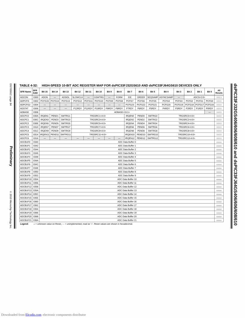
ds
PIC
33
FJ
32
GS
40
6/6
06
/60
8/6
10
an
d d
sP
IC3
3F
J6
4G
S4
06
/60
6/6
08/6
10
DS
70
59
1C
-pa
ge
84
Prelim
ina
ry
20
10
Micro
chip
Te
chn
olo
gy In
c.
TABLE 4-32: HIGH-SPEED 10-BIT ADC REGISTER MAP FOR dsPIC33FJ32GS610 AND dsPIC33FJ64GS610 DEVICES ONLY
SFR NameSFR Addr
Bit 15 Bit 14 Bit 13 Bit 12 Bit 11 Bit 10 Bit 9 Bit 8 Bit 7 Bit 6 Bit 5 Bit 4 Bit 3 Bit 2 Bit 1 Bit 0All
Resets
ADCON 0300 ADON — ADSIDL SLOWCLK — GSWTRG — FORM EIE ORDER SEQSAMP ASYNCSAMP — ADCS<2:0> 0003
ADPCFG 0302 PCFG15 PCFG14 PCFG13 PCFG12 PCFG11 PCFG10 PCFG9 PCFG8 PCFG7 PCFG6 PCFG5 PCFG4 PCFG3 PCFG2 PCFG1 PCFG0 0000
ADPCFG2 0304 — — — — — — — — PCFG23 PCFG22 PCFG21 PCFG20 PCFG19 PCFG18 PCFG17 PCFG16 0000
ADSTAT 0306 — — — P12RDY P11RDY P10RDY P9RDY P8RDY P7RDY P6RDY P5RDY P4RDY P3RDY P2RDY P1RDY P0RDY 0000
ADBASE 0308 ADBASE<15:1> — 0000
ADCPC0 030A IRQEN1 PEND1 SWTRG1 TRGSRC1<4:0> IRQEN0 PEND0 SWTRG0 TRGSRC0<4:0> 0000
ADCPC1 030C IRQEN3 PEND3 SWTRG3 TRGSRC3<4:0> IRQEN2 PEND2 SWTRG2 TRGSRC2<4:0> 0000
ADCPC2 030E IRQEN5 PEND5 SWTRG5 TRGSRC5<4:0> IRQEN4 PEND4 SWTRG4 TRGSRC4<4:0> 0000
ADCPC3 0310 IRQEN7 PEND7 SWTRG7 TRGSRC7<4:0> IRQEN6 PEND6 SWTRG6 TRGSRC6<4:0> 0000
ADCPC4 0312 IRQEN9 PEND9 SWTRG9 TRGSRC9<4:0> IRQEN8 PEND8 SWTRG8 TRGSRC8<4:0> 0000
ADCPC5 0314 IRQEN11 PEND11 SWTRG11 TRGSRC11<4:0> IRQEN10 PEND10 SWTRG10 TRGSRC10<4:0> 0000
ADCPC6 0316 — — — — — — — — IRQEN12 PEND12 SWTRG12 TRGSRC12<4:0> 0000
ADCBUF0 0340 ADC Data Buffer 0 xxxx
ADCBUF1 0342 ADC Data Buffer 1 xxxx
ADCBUF2 0344 ADC Data Buffer 2 xxxx
ADCBUF3 0346 ADC Data Buffer 3 xxxx
ADCBUF4 0348 ADC Data Buffer 4 xxxx
ADCBUF5 034A ADC Data Buffer 5 xxxx
ADCBUF6 034C ADC Data Buffer 6 xxxx
ADCBUF7 034E ADC Data Buffer 7 xxxx
ADCBUF8 0350 ADC Data Buffer 8 xxxx
ADCBUF9 0352 ADC Data Buffer 9 xxxx
ADCBUF10 0354 ADC Data Buffer 10 xxxx
ADCBUF11 0356 ADC Data Buffer 11 xxxx
ADCBUF12 0358 ADC Data Buffer 12 xxxx
ADCBUF13 035A ADC Data Buffer 13 xxxx
ADCBUF14 035C ADC Data Buffer 14 xxxx
ADCBUF15 035E ADC Data Buffer 15 xxxx
ADCBUF16 0360 ADC Data Buffer 16 xxxx
ADCBUF17 0362 ADC Data Buffer 17 xxxx
ADCBUF18 0364 ADC Data Buffer 18 xxxx
ADCBUF19 0366 ADC Data Buffer 19 xxxx
ADCBUF20 0368 ADC Data Buffer 20 xxxx
ADCBUF21 036A ADC Data Buffer 21 xxxx
Legend: x = unknown value on Reset, — = unimplemented, read as ‘0’. Reset values are shown in hexadecimal.
Downloaded from Elcodis.com electronic components distributor
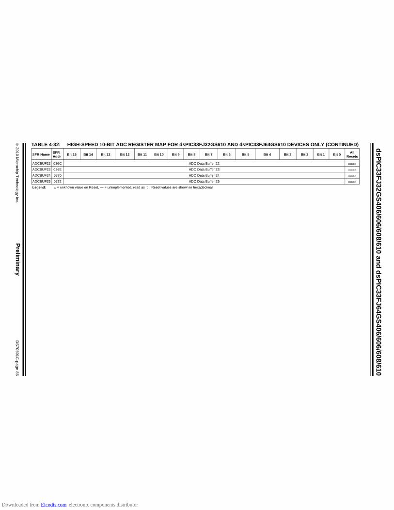
2
01
0 M
icroch
ip T
ech
no
log
y Inc.
Prelim
inary
DS
70
59
1C
-pa
ge
85
ds
PIC
33
FJ
32
GS
40
6/6
06/6
08/6
10 a
nd
ds
PIC
33
FJ
64G
S4
06/6
06/60
8/61
0
ADCBUF22 036C ADC Data Buffer 22 xxxx
ADCBUF23 036E ADC Data Buffer 23 xxxx
ADCBUF24 0370 ADC Data Buffer 24 xxxx
ADCBUF25 0372 ADC Data Buffer 25 xxxx
TABLE 4-32: HIGH-SPEED 10-BIT ADC REGISTER MAP FOR dsPIC33FJ32GS610 AND dsPIC33FJ64GS610 DEVICES ONLY (CONTINUED)
SFR NameSFR Addr
Bit 15 Bit 14 Bit 13 Bit 12 Bit 11 Bit 10 Bit 9 Bit 8 Bit 7 Bit 6 Bit 5 Bit 4 Bit 3 Bit 2 Bit 1 Bit 0All
Resets
Legend: x = unknown value on Reset, — = unimplemented, read as ‘0’. Reset values are shown in hexadecimal.
Downloaded from Elcodis.com electronic components distributor
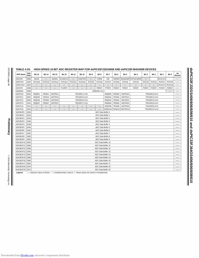
ds
PIC
33
FJ
32
GS
40
6/6
06
/60
8/6
10
an
d d
sP
IC3
3F
J6
4G
S4
06
/60
6/6
08/6
10
DS
70
59
1C
-pa
ge
86
Prelim
ina
ry
20
10
Micro
chip
Te
chn
olo
gy In
c.
TABLE 4-33: HIGH-SPEED 10-BIT ADC REGISTER MAP FOR dsPIC33FJ32GS608 AND dsPIC33FJ64GS608 DEVICES
SFR NameSFR Addr
Bit 15 Bit 14 Bit 13 Bit 12 Bit 11 Bit 10 Bit 9 Bit 8 Bit 7 Bit 6 Bit 5 Bit 4 Bit 3 Bit 2 Bit 1 Bit 0All
Resets
ADCON 0300 ADON — ADSIDL SLOWCLK — GSWTRG — FORM EIE ORDER SEQSAMP ASYNCSAMP — ADCS<2:0> 0003
ADPCFG 0302 PCFG15 PCFG14 PCFG13 PCFG12 PCFG11 PCFG10 PCFG9 PCFG8 PCFG7 PCFG6 PCFG5 PCFG4 PCFG3 PCFG2 PCFG1 PCFG0 0000
ADPCFG2 0304 — — — — — — — — — — — — — — PCFG17 PCFG16 0000
ADSTAT 0306 — — — P12RDY — — — P8RDY P7RDY P6RDY P5RDY P4RDY P3RDY P2RDY P1RDY P0RDY 0000
ADBASE 0308 ADBASE<15:1> — 0000
ADCPC0 030A IRQEN1 PEND1 SWTRG1 TRGSRC1<4:0> IRQEN0 PEND0 SWTRG0 TRGSRC0<4:0> 0000
ADCPC1 030C IRQEN3 PEND3 SWTRG3 TRGSRC3<4:0> IRQEN2 PEND2 SWTRG2 TRGSRC2<4:0> 0000
ADCPC2 030E IRQEN5 PEND5 SWTRG5 TRGSRC5<4:0> IRQEN4 PEND4 SWTRG4 TRGSRC4<4:0> 0000
ADCPC3 0310 IRQEN7 PEND7 SWTRG7 TRGSRC7<4:0> IRQEN6 PEND6 SWTRG6 TRGSRC6<4:0> 0000
ADCPC4 0312 — — — — — — — — IRQEN8 PEND8 SWTRG8 TRGSRC8<4:0> 0000
ADCPC6 0316 — — — — — — — — IRQEN12 PEND12 SWTRG12 TRGSRC12<4:0> 0000
ADCBUF0 0340 ADC Data Buffer 0 xxxx
ADCBUF1 0342 ADC Data Buffer 1 xxxx
ADCBUF2 0344 ADC Data Buffer 2 xxxx
ADCBUF3 0346 ADC Data Buffer 3 xxxx
ADCBUF4 0348 ADC Data Buffer 4 xxxx
ADCBUF5 034A ADC Data Buffer 5 xxxx
ADCBUF6 034C ADC Data Buffer 6 xxxx
ADCBUF7 034E ADC Data Buffer 7 xxxx
ADCBUF8 0350 ADC Data Buffer 8 xxxx
ADCBUF9 0352 ADC Data Buffer 9 xxxx
ADCBUF10 0354 ADC Data Buffer 10 xxxx
ADCBUF11 0356 ADC Data Buffer 11 xxxx
ADCBUF12 0358 ADC Data Buffer 12 xxxx
ADCBUF13 035A ADC Data Buffer 13 xxxx
ADCBUF14 035C ADC Data Buffer 14 xxxx
ADCBUF15 035E ADC Data Buffer 15 xxxx
ADCBUF16 0360 ADC Data Buffer 16 xxxx
ADCBUF17 0362 ADC Data Buffer 17 xxxx
ADCBUF24 0370 ADC Data Buffer 24 xxxx
ADCBUF25 0372 ADC Data Buffer 25 xxxx
Legend: x = unknown value on Reset, — = unimplemented, read as ‘0’. Reset values are shown in hexadecimal.
Downloaded from Elcodis.com electronic components distributor
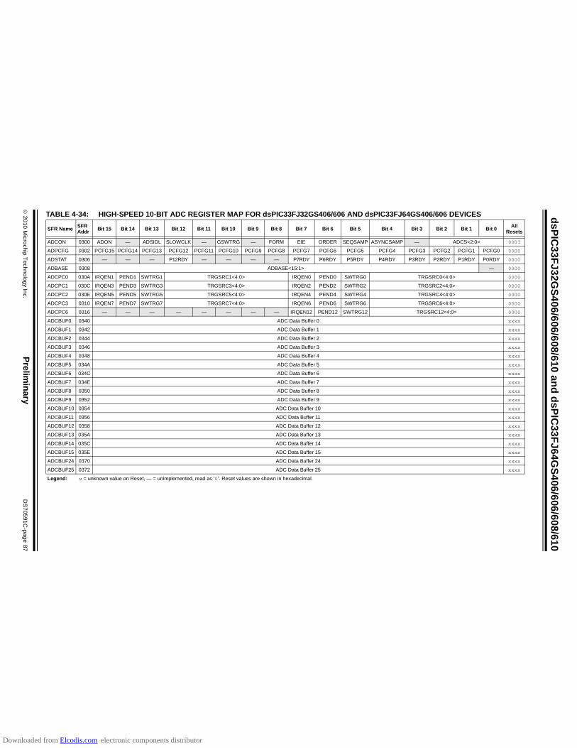
2
01
0 M
icroch
ip T
ech
no
log
y Inc.
Prelim
inary
DS
70
59
1C
-pa
ge
87
ds
PIC
33
FJ
32
GS
40
6/6
06/6
08/6
10 a
nd
ds
PIC
33
FJ
64G
S4
06/6
06/60
8/61
0
TABLE 4-34: HIGH-SPEED 10-BIT ADC REGISTER MAP FOR dsPIC33FJ32GS406/606 AND dsPIC33FJ64GS406/606 DEVICES
SFR NameSFR Addr
Bit 15 Bit 14 Bit 13 Bit 12 Bit 11 Bit 10 Bit 9 Bit 8 Bit 7 Bit 6 Bit 5 Bit 4 Bit 3 Bit 2 Bit 1 Bit 0All
Resets
ADCON 0300 ADON — ADSIDL SLOWCLK — GSWTRG — FORM EIE ORDER SEQSAMP ASYNCSAMP — ADCS<2:0> 0003
ADPCFG 0302 PCFG15 PCFG14 PCFG13 PCFG12 PCFG11 PCFG10 PCFG9 PCFG8 PCFG7 PCFG6 PCFG5 PCFG4 PCFG3 PCFG2 PCFG1 PCFG0 0000
ADSTAT 0306 — — — P12RDY — — — — P7RDY P6RDY P5RDY P4RDY P3RDY P2RDY P1RDY P0RDY 0000
ADBASE 0308 ADBASE<15:1> — 0000
ADCPC0 030A IRQEN1 PEND1 SWTRG1 TRGSRC1<4:0> IRQEN0 PEND0 SWTRG0 TRGSRC0<4:0> 0000
ADCPC1 030C IRQEN3 PEND3 SWTRG3 TRGSRC3<4:0> IRQEN2 PEND2 SWTRG2 TRGSRC2<4:0> 0000
ADCPC2 030E IRQEN5 PEND5 SWTRG5 TRGSRC5<4:0> IRQEN4 PEND4 SWTRG4 TRGSRC4<4:0> 0000
ADCPC3 0310 IRQEN7 PEND7 SWTRG7 TRGSRC7<4:0> IRQEN6 PEND6 SWTRG6 TRGSRC6<4:0> 0000
ADCPC6 0316 — — — — — — — — IRQEN12 PEND12 SWTRG12 TRGSRC12<4:0> 0000
ADCBUF0 0340 ADC Data Buffer 0 xxxx
ADCBUF1 0342 ADC Data Buffer 1 xxxx
ADCBUF2 0344 ADC Data Buffer 2 xxxx
ADCBUF3 0346 ADC Data Buffer 3 xxxx
ADCBUF4 0348 ADC Data Buffer 4 xxxx
ADCBUF5 034A ADC Data Buffer 5 xxxx
ADCBUF6 034C ADC Data Buffer 6 xxxx
ADCBUF7 034E ADC Data Buffer 7 xxxx
ADCBUF8 0350 ADC Data Buffer 8 xxxx
ADCBUF9 0352 ADC Data Buffer 9 xxxx
ADCBUF10 0354 ADC Data Buffer 10 xxxx
ADCBUF11 0356 ADC Data Buffer 11 xxxx
ADCBUF12 0358 ADC Data Buffer 12 xxxx
ADCBUF13 035A ADC Data Buffer 13 xxxx
ADCBUF14 035C ADC Data Buffer 14 xxxx
ADCBUF15 035E ADC Data Buffer 15 xxxx
ADCBUF24 0370 ADC Data Buffer 24 xxxx
ADCBUF25 0372 ADC Data Buffer 25 xxxx
Legend: x = unknown value on Reset, — = unimplemented, read as ‘0’. Reset values are shown in hexadecimal.
Downloaded from Elcodis.com electronic components distributor

ds
PIC
33
FJ
32
GS
40
6/6
06
/60
8/6
10
an
d d
sP
IC3
3F
J6
4G
S4
06
/60
6/6
08/6
10
DS
70
59
1C
-pa
ge
88
Prelim
ina
ry
20
10
Micro
chip
Te
chn
olo
gy In
c.
TABLE 4-35: DMA REGISTER MAP
File Name Addr Bit 15 Bit 14 Bit 13 Bit 12 Bit 11 Bit 10 Bit 9 Bit 8 Bit 7 Bit 6 Bit 5 Bit 4 Bit 3 Bit 2 Bit 1 Bit 0All
Resets
DMA0CON 0380 CHEN SIZE DIR HALF NULLW — — — — — AMODE<1:0> — — MODE<1:0> 0000
DMA0REQ 0382 FORCE — — — — — — — — IRQSEL<6:0> 007F
DMA0STA 0384 STA<15:0> 0000
DMA0STB 0386 STB<15:0> 0000
DMA0PAD 0388 PAD<15:0> 0000
DMA0CNT 038A — — — — — — CNT<9:0> 0000
DMA1CON 038C CHEN SIZE DIR HALF NULLW — — — — — AMODE<1:0> — — MODE<1:0> 0000
DMA1REQ 038E FORCE — — — — — — — — IRQSEL<6:0> 007F
DMA1STA 0390 STA<15:0> 0000
DMA1STB 0392 STB<15:0> 0000
DMA1PAD 0394 PAD<15:0> 0000
DMA1CNT 0396 — — — — — — CNT<9:0> 0000
DMA2CON 0398 CHEN SIZE DIR HALF NULLW — — — — — AMODE<1:0> — — MODE<1:0> 0000
DMA2REQ 039A FORCE — — — — — — — — IRQSEL<6:0> 007F
DMA2STA 039C STA<15:0> 0000
DMA2STB 039E STB<15:0> 0000
DMA2PAD 03A0 PAD<15:0> 0000
DMA2CNT 03A2 — — — — — — CNT<9:0> 0000
DMA3CON 03A4 CHEN SIZE DIR HALF NULLW — — — — — AMODE<1:0> — — MODE<1:0> 0000
DMA3REQ 03A6 FORCE — — — — — — — — IRQSEL<6:0> 007F
DMA3STA 03A8 STA<15:0> 0000
DMA3STB 03AA STB<15:0> 0000
DMA3PAD 03AC PAD<15:0> 0000
DMA3CNT 03AE — — — — — — CNT<9:0> 0000
DMACS0 03E0 — — — — PWCOL3 PWCOL2 PWCOL1 PWCOL0 — — — — XWCOL3 XWCOL2 XWCOL1 XWCOL0 0000
DMACS1 03E2 — — — — LSTCH<3:0> — — — — PPST3 PPST2 PPST1 PPST0 0F00
DSADR 03E4 DSADR<15:0> 0000
Legend: — = unimplemented, read as ‘0’. Reset values are shown in hexadecimal.
Downloaded from Elcodis.com electronic components distributor

2
01
0 M
icroch
ip T
ech
no
log
y Inc.
Prelim
inary
DS
70
59
1C
-pa
ge
89
ds
PIC
33
FJ
32
GS
40
6/6
06/6
08/6
10 a
nd
ds
PIC
33
FJ
64G
S4
06/6
06/60
8/61
0
TABLE 4-36: ECAN1 REGISTER MAP WHEN C1CTRL1.WIN = 0 OR 1
File Name Addr Bit 15 Bit 14 Bit 13 Bit 12 Bit 11 Bit 10 Bit 9 Bit 8 Bit 7 Bit 6 Bit 5 Bit 4 Bit 3 Bit 2 Bit 1 Bit 0All
Resets
C1CTRL1 0600 — — CSIDL ABAT — REQOP<2:0> OPMODE<2:0> — CANCAP — — WIN 0480
C1CTRL2 0602 — — — — — — — — — — — DNCNT<4:0> 0000
C1VEC 0604 — — — FILHIT<4:0> — ICODE<6:0> 0000
C1FCTRL 0606 DMABS<2:0> — — — — — — — — FSA<4:0> 0000
C1FIFO 0608 — — FBP<5:0> — — FNRB<5:0> 0000
C1INTF 060A — — TXBO TXBP RXBP TXWAR RXWAR EWARN IVRIF WAKIF ERRIF — FIFOIF RBOVIF RBIF TBIF 0000
C1INTE 060C — — — — — — — — IVRIE WAKIE ERRIE — FIFOIE RBOVIE RBIE TBIE 0000
C1EC 060E TERRCNT<7:0> RERRCNT<7:0> 0000
C1CFG1 0610 — — — — — — — — SJW<1:0> BRP<5:0> 0000
C1CFG2 0612 — WAKFIL — — — SEG2PH<2:0> SEG2PHTS SAM SEG1PH<2:0> PRSEG<2:0> 0000
C1FEN1 0614 FLTEN15 FLTEN14 FLTEN13 FLTEN12 FLTEN11 FLTEN10 FLTEN9 FLTEN8 FLTEN7 FLTEN6 FLTEN5 FLTEN4 FLTEN3 FLTEN2 FLTEN1 FLTEN0 FFFF
C1FMSKSEL1 0618 F7MSK<1:0> F6MSK<1:0> F5MSK<1:0> F4MSK<1:0> F3MSK<1:0> F2MSK<1:0> F1MSK<1:0> F0MSK<1:0> 0000
C1FMSKSEL2 061A F15MSK<1:0> F14MSK<1:0> F13MSK<1:0> F12MSK<1:0> F11MSK<1:0> F10MSK<1:0> F9MSK<1:0> F8MSK<1:0> 0000
Legend: — = unimplemented, read as ‘0’. Reset values are shown in hexadecimal.
TABLE 4-37: ECAN1 REGISTER MAP WHEN C1CTRL1.WIN = 0
File Name Addr Bit 15 Bit 14 Bit 13 Bit 12 Bit 11 Bit 10 Bit 9 Bit 8 Bit 7 Bit 6 Bit 5 Bit 4 Bit 3 Bit 2 Bit 1 Bit 0All
Resets
0600-061E
See definition when WIN = x
C1RXFUL1 0620 RXFUL15 RXFUL14 RXFUL13 RXFUL12 RXFUL11 RXFUL10 RXFUL9 RXFUL8 RXFUL7 RXFUL6 RXFUL5 RXFUL4 RXFUL3 RXFUL2 RXFUL1 RXFUL0 0000
C1RXFUL2 0622 RXFUL31 RXFUL30 RXFUL29 RXFUL28 RXFUL27 RXFUL26 RXFUL25 RXFUL24 RXFUL23 RXFUL22 RXFUL21 RXFUL20 RXFUL19 RXFUL18 RXFUL17 RXFUL16 0000
C1RXOVF1 0628 RXOVF15 RXOVF14 RXOVF13 RXOVF12 RXOVF11 RXOVF10 RXOVF9 RXOVF8 RXOVF7 RXOVF6 RXOVF5 RXOVF4 RXOVF3 RXOVF2 RXOVF1 RXOVF0 0000
C1RXOVF2 062A RXOVF31 RXOVF30 RXOVF29 RXOVF28 RXOVF27 RXOVF26 RXOVF25 RXOVF24 RXOVF23 RXOVF22 RXOVF21 RXOVF20 RXOVF19 RXOVF18 RXOVF17 RXOVF16 0000
C1TR01CON 0630 TXEN1 TXABT1 TXLARB1 TXERR1 TXREQ1 RTREN1 TX1PRI<1:0> TXEN0 TXABT0 TXLARB0 TXERR0 TXREQ0 RTREN0 TX0PRI<1:0> 0000
C1TR23CON 0632 TXEN3 TXABT3 TXLARB3 TXERR3 TXREQ3 RTREN3 TX3PRI<1:0> TXEN2 TXABT2 TXLARB2 TXERR2 TXREQ2 RTREN2 TX2PRI<1:0> 0000
C1TR45CON 0634 TXEN5 TXABT5 TXLARB5 TXERR5 TXREQ5 RTREN5 TX5PRI<1:0> TXEN4 TXABT4 TXLARB4 TXERR4 TXREQ4 RTREN4 TX4PRI<1:0> 0000
C1TR67CON 0636 TXEN7 TXABT7 TXLARB7 TXERR7 TXREQ7 RTREN7 TX7PRI<1:0> TXEN6 TXABT6 TXLARB6 TXERR6 TXREQ6 RTREN6 TX6PRI<1:0> 0000
C1RXD 0640 Received Data Word xxxx
C1TXD 0642 Transmit Data Word xxxx
Legend: x = unknown value on Reset, — = unimplemented, read as ‘0’. Reset values are shown in hexadecimal.
Downloaded from Elcodis.com electronic components distributor

ds
PIC
33
FJ
32
GS
40
6/6
06
/60
8/6
10
an
d d
sP
IC3
3F
J6
4G
S4
06
/60
6/6
08/6
10
DS
70
59
1C
-pa
ge
90
Prelim
ina
ry
20
10
Micro
chip
Te
chn
olo
gy In
c.
TABLE 4-38: ECAN1 REGISTER MAP WHEN C1CTRL1.WIN = 1
File Name Addr Bit 15 Bit 14 Bit 13 Bit 12 Bit 11 Bit 10 Bit 9 Bit 8 Bit 7 Bit 6 Bit 5 Bit 4 Bit 3 Bit 2 Bit 1 Bit 0All
Resets
0600-061E
See definition when WIN = x
C1BUFPNT1 0620 F3BP<3:0> F2BP<3:0> F1BP<3:0> F0BP<3:0> 0000
C1BUFPNT2 0622 F7BP<3:0> F6BP<3:0> F5BP<3:0> F4BP<3:0> 0000
C1BUFPNT3 0624 F11BP<3:0> F10BP<3:0> F9BP<3:0> F8BP<3:0> 0000
C1BUFPNT4 0626 F15BP<3:0> F14BP<3:0> F13BP<3:0> F12BP<3:0> 0000
C1RXM0SID 0630 SID<10:3> SID<2:0> — MIDE — EID<17:16> xxxx
C1RXM0EID 0632 EID<15:8> EID<7:0> xxxx
C1RXM1SID 0634 SID<10:3> SID<2:0> — MIDE — EID<17:16> xxxx
C1RXM1EID 0636 EID<15:8> EID<7:0> xxxx
C1RXM2SID 0638 SID<10:3> SID<2:0> — MIDE — EID<17:16> xxxx
C1RXM2EID 063A EID<15:8> EID<7:0> xxxx
C1RXF0SID 0640 SID<10:3> SID<2:0> — EXIDE — EID<17:16> xxxx
C1RXF0EID 0642 EID<15:8> EID<7:0> xxxx
C1RXF1SID 0644 SID<10:3> SID<2:0> — EXIDE — EID<17:16> xxxx
C1RXF1EID 0646 EID<15:8> EID<7:0> xxxx
C1RXF2SID 0648 SID<10:3> SID<2:0> — EXIDE — EID<17:16> xxxx
C1RXF2EID 064A EID<15:8> EID<7:0> xxxx
C1RXF3SID 064C SID<10:3> SID<2:0> — EXIDE — EID<17:16> xxxx
C1RXF3EID 064E EID<15:8> EID<7:0> xxxx
C1RXF4SID 0650 SID<10:3> SID<2:0> — EXIDE — EID<17:16> xxxx
C1RXF4EID 0652 EID<15:8> EID<7:0> xxxx
C1RXF5SID 0654 SID<10:3> SID<2:0> — EXIDE — EID<17:16> xxxx
C1RXF5EID 0656 EID<15:8> EID<7:0> xxxx
C1RXF6SID 0658 SID<10:3> SID<2:0> — EXIDE — EID<17:16> xxxx
C1RXF6EID 065A EID<15:8> EID<7:0> xxxx
C1RXF7SID 065C SID<10:3> SID<2:0> — EXIDE — EID<17:16> xxxx
C1RXF7EID 065E EID<15:8> EID<7:0> xxxx
C1RXF8SID 0660 SID<10:3> SID<2:0> — EXIDE — EID<17:16> xxxx
C1RXF8EID 0662 EID<15:8> EID<7:0> xxxx
C1RXF9SID 0664 SID<10:3> SID<2:0> — EXIDE — EID<17:16> xxxx
C1RXF9EID 0666 EID<15:8> EID<7:0> xxxx
C1RXF10SID 0668 SID<10:3> SID<2:0> — EXIDE — EID<17:16> xxxx
C1RXF10EID 066A EID<15:8> EID<7:0> xxxx
C1RXF11SID 066C SID<10:3> SID<2:0> — EXIDE — EID<17:16> xxxx
Legend: x = unknown value on Reset, — = unimplemented, read as ‘0’. Reset values are shown in hexadecimal.
Downloaded from Elcodis.com electronic components distributor
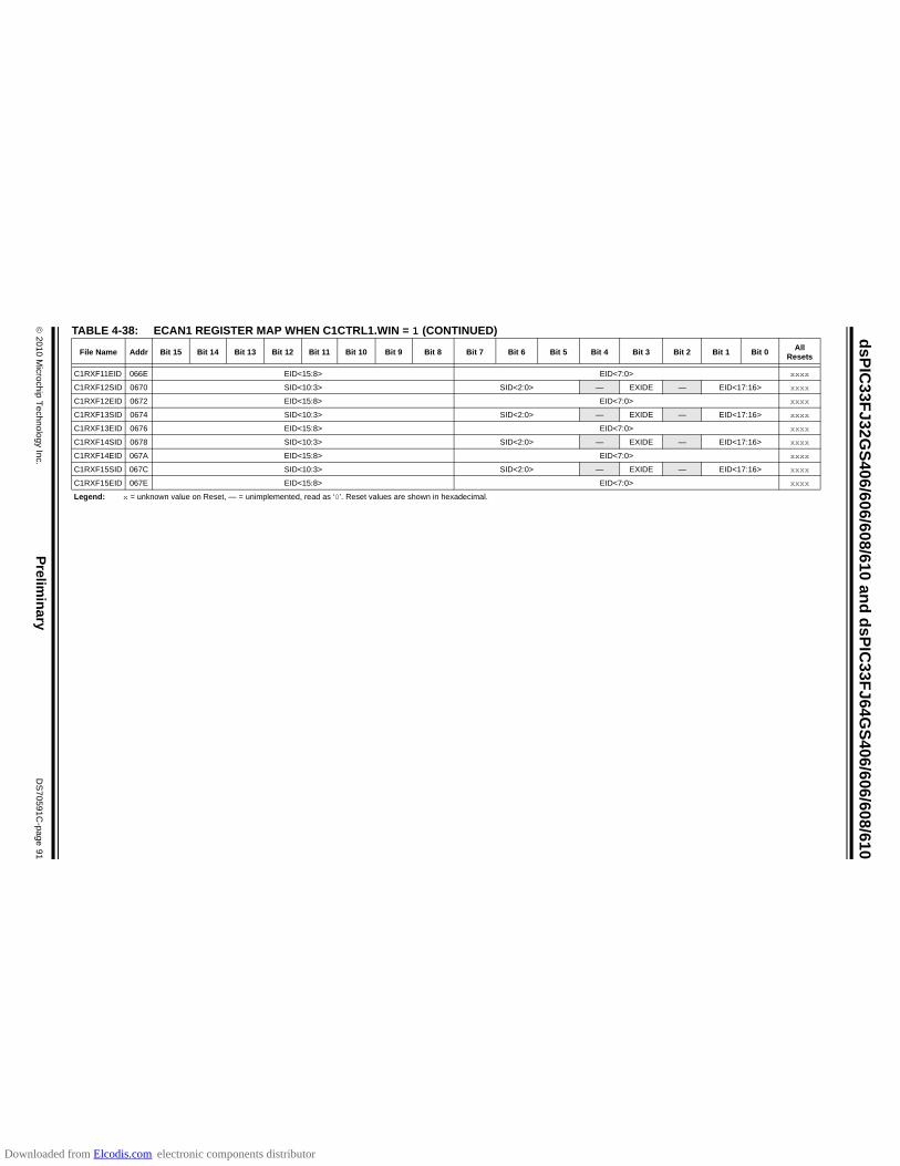
2
01
0 M
icroch
ip T
ech
no
log
y Inc.
Prelim
inary
DS
70
59
1C
-pa
ge
91
ds
PIC
33
FJ
32
GS
40
6/6
06/6
08/6
10 a
nd
ds
PIC
33
FJ
64G
S4
06/6
06/60
8/61
0
C1RXF11EID 066E EID<15:8> EID<7:0> xxxx
C1RXF12SID 0670 SID<10:3> SID<2:0> — EXIDE — EID<17:16> xxxx
C1RXF12EID 0672 EID<15:8> EID<7:0> xxxx
C1RXF13SID 0674 SID<10:3> SID<2:0> — EXIDE — EID<17:16> xxxx
C1RXF13EID 0676 EID<15:8> EID<7:0> xxxx
C1RXF14SID 0678 SID<10:3> SID<2:0> — EXIDE — EID<17:16> xxxx
C1RXF14EID 067A EID<15:8> EID<7:0> xxxx
C1RXF15SID 067C SID<10:3> SID<2:0> — EXIDE — EID<17:16> xxxx
C1RXF15EID 067E EID<15:8> EID<7:0> xxxx
TABLE 4-38: ECAN1 REGISTER MAP WHEN C1CTRL1.WIN = 1 (CONTINUED)
File Name Addr Bit 15 Bit 14 Bit 13 Bit 12 Bit 11 Bit 10 Bit 9 Bit 8 Bit 7 Bit 6 Bit 5 Bit 4 Bit 3 Bit 2 Bit 1 Bit 0All
Resets
Legend: x = unknown value on Reset, — = unimplemented, read as ‘0’. Reset values are shown in hexadecimal.
Downloaded from Elcodis.com electronic components distributor
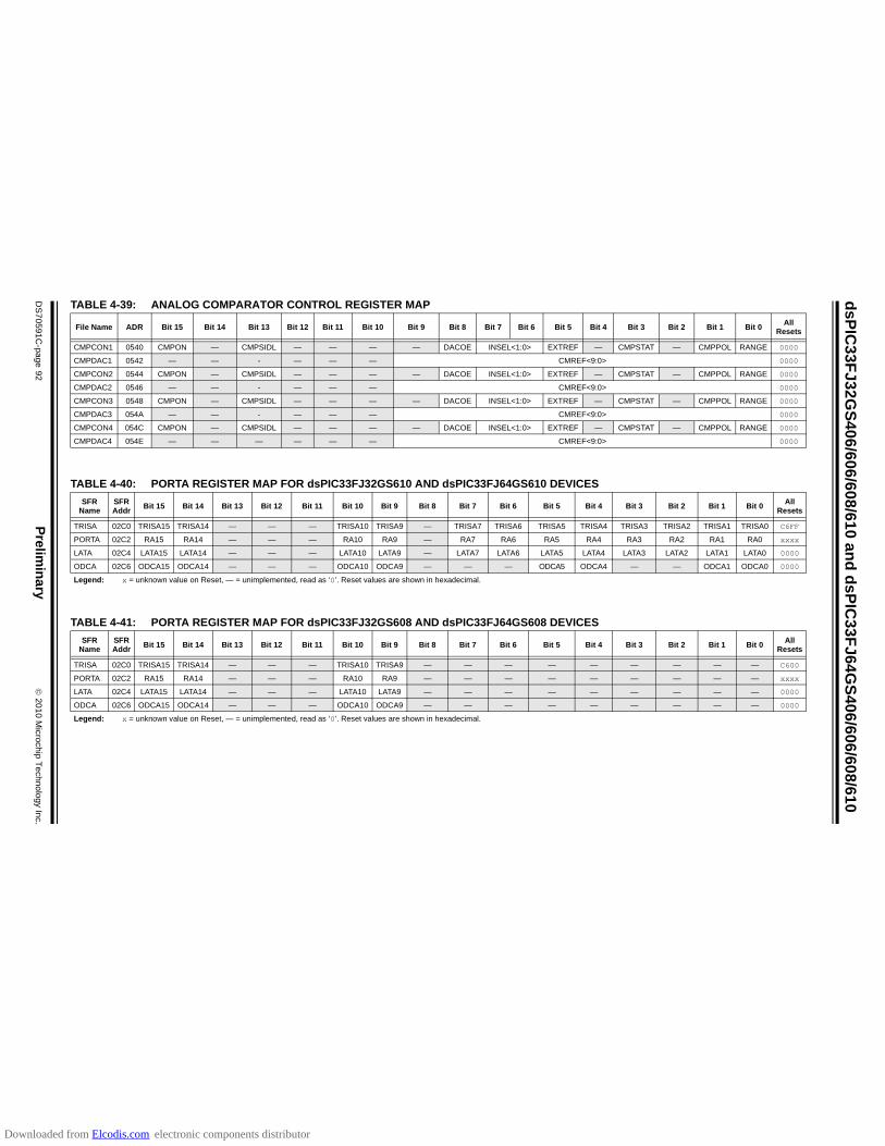
ds
PIC
33
FJ
32
GS
40
6/6
06
/60
8/6
10
an
d d
sP
IC3
3F
J6
4G
S4
06
/60
6/6
08/6
10
DS
70
59
1C
-pa
ge
92
Prelim
ina
ry
20
10
Micro
chip
Te
chn
olo
gy In
c.
TABLE 4-39: ANALOG COMPARATOR CONTROL REGISTER MAP
TABLE 4-40: PORTA REGISTER MAP FOR dsPIC33FJ32GS610 AND dsPIC33FJ64GS610 DEVICES
TABLE 4-41: PORTA REGISTER MAP FOR dsPIC33FJ32GS608 AND dsPIC33FJ64GS608 DEVICES
File Name ADR Bit 15 Bit 14 Bit 13 Bit 12 Bit 11 Bit 10 Bit 9 Bit 8 Bit 7 Bit 6 Bit 5 Bit 4 Bit 3 Bit 2 Bit 1 Bit 0All
Resets
CMPCON1 0540 CMPON — CMPSIDL — — — — DACOE INSEL<1:0> EXTREF — CMPSTAT — CMPPOL RANGE 0000
CMPDAC1 0542 — — - — — — CMREF<9:0> 0000
CMPCON2 0544 CMPON — CMPSIDL — — — — DACOE INSEL<1:0> EXTREF — CMPSTAT — CMPPOL RANGE 0000
CMPDAC2 0546 — — - — — — CMREF<9:0> 0000
CMPCON3 0548 CMPON — CMPSIDL — — — — DACOE INSEL<1:0> EXTREF — CMPSTAT — CMPPOL RANGE 0000
CMPDAC3 054A — — - — — — CMREF<9:0> 0000
CMPCON4 054C CMPON — CMPSIDL — — — — DACOE INSEL<1:0> EXTREF — CMPSTAT — CMPPOL RANGE 0000
CMPDAC4 054E — — — — — — CMREF<9:0> 0000
SFR Name
SFR Addr
Bit 15 Bit 14 Bit 13 Bit 12 Bit 11 Bit 10 Bit 9 Bit 8 Bit 7 Bit 6 Bit 5 Bit 4 Bit 3 Bit 2 Bit 1 Bit 0All
Resets
TRISA 02C0 TRISA15 TRISA14 — — — TRISA10 TRISA9 — TRISA7 TRISA6 TRISA5 TRISA4 TRISA3 TRISA2 TRISA1 TRISA0 C6FF
PORTA 02C2 RA15 RA14 — — — RA10 RA9 — RA7 RA6 RA5 RA4 RA3 RA2 RA1 RA0 xxxx
LATA 02C4 LATA15 LATA14 — — — LATA10 LATA9 — LATA7 LATA6 LATA5 LATA4 LATA3 LATA2 LATA1 LATA0 0000
ODCA 02C6 ODCA15 ODCA14 — — — ODCA10 ODCA9 — — — ODCA5 ODCA4 — — ODCA1 ODCA0 0000
Legend: x = unknown value on Reset, — = unimplemented, read as ‘0’. Reset values are shown in hexadecimal.
SFR Name
SFR Addr
Bit 15 Bit 14 Bit 13 Bit 12 Bit 11 Bit 10 Bit 9 Bit 8 Bit 7 Bit 6 Bit 5 Bit 4 Bit 3 Bit 2 Bit 1 Bit 0All
Resets
TRISA 02C0 TRISA15 TRISA14 — — — TRISA10 TRISA9 — — — — — — — — — C600
PORTA 02C2 RA15 RA14 — — — RA10 RA9 — — — — — — — — — xxxx
LATA 02C4 LATA15 LATA14 — — — LATA10 LATA9 — — — — — — — — — 0000
ODCA 02C6 ODCA15 ODCA14 — — — ODCA10 ODCA9 — — — — — — — — — 0000
Legend: x = unknown value on Reset, — = unimplemented, read as ‘0’. Reset values are shown in hexadecimal.
Downloaded from Elcodis.com electronic components distributor

2
01
0 M
icroch
ip T
ech
no
log
y Inc.
Prelim
inary
DS
70
59
1C
-pa
ge
93
ds
PIC
33
FJ
32
GS
40
6/6
06/6
08/6
10 a
nd
ds
PIC
33
FJ
64G
S4
06/6
06/60
8/61
0
TABLE 4-42: PORTB REGISTER MAP
TABLE 4-43: PORTC REGISTER MAP FOR dsPIC33FJ32GS610 AND dsPIC33FJ64GS610 DEVICES
TABLE 4-44: PORTC REGISTER MAP FOR dsPIC33FJ32GS608 AND dsPIC33FJ64GS608 DEVICES
TABLE 4-45: PORTC REGISTER MAP FOR dsPIC33FJ32GS406/606 AND dsPIC33FJ64GS406/606 DEVICES
SFR Name
SFR Addr
Bit 15 Bit 14 Bit 13 Bit 12 Bit 11 Bit 10 Bit 9 Bit 8 Bit 7 Bit 6 Bit 5 Bit 4 Bit 3 Bit 2 Bit 1 Bit 0All
Resets
TRISB 02C8 TRISB15 TRISB14 TRISB13 TRISB12 TRISB11 TRISB10 TRISB9 TRISB8 TRISB7 TRISB6 TRISB5 TRISB4 TRISB3 TRISB2 TRISB1 TRISB0 FFFF
PORTB 02CA RB15 RB14 RB13 RB12 RB11 RB10 RB9 RB8 RB7 RB6 RB5 RB4 RB3 RB2 RB1 RB0 xxxx
LATB 02CC LATB15 LATB14 LATB13 LATB12 LATB11 LATB10 LATB9 LATB8 LATB7 LATB6 LATB5 LATB4 LATB3 LATB2 LATB1 LATB0 0000
Legend: x = unknown value on Reset, — = unimplemented, read as ‘0’. Reset values are shown in hexadecimal.
SFR Name
SFR Addr
Bit 15 Bit 14 Bit 13 Bit 12 Bit 11 Bit 10 Bit 9 Bit 8 Bit 7 Bit 6 Bit 5 Bit 4 Bit 3 Bit 2 Bit 1 Bit 0All
Resets
TRISC 02D0 TRISC15 TRISC14 TRISC13 TRISC12 — — — — — — — TRISC4 TRISC3 TRISC2 TRISC1 — F01E
PORTC 02D2 RC15 RC14 RC13 RC12 — — — — — — — RC4 RC3 RC2 RC1 — xxxx
LATC 02D4 LATC15 LATC14 LATC13 LATC12 — — — — — — — LATC4 LATC3 LATC2 LATC1 — 0000
Legend: x = unknown value on Reset, — = unimplemented, read as ‘0’. Reset values are shown in hexadecimal.
SFR Name
SFR Addr
Bit 15 Bit 14 Bit 13 Bit 12 Bit 11 Bit 10 Bit 9 Bit 8 Bit 7 Bit 6 Bit 5 Bit 4 Bit 3 Bit 2 Bit 1 Bit 0All
Resets
TRISC 02D0 TRISC15 TRISC14 TRISC13 TRISC12 — — — — — — — — — TRISC2 TRISC1 — F006
PORTC 02D2 RC15 RC14 RC13 RC12 — — — — — — — — — RC2 RC1 — xxxx
LATC 02D4 LATC15 LATC14 LATC13 LATC12 — — — — — — — — — LATC2 LATC1 — 0000
Legend: x = unknown value on Reset, — = unimplemented, read as ‘0’. Reset values are shown in hexadecimal.
SFR Name
SFR Addr
Bit 15 Bit 14 Bit 13 Bit 12 Bit 11 Bit 10 Bit 9 Bit 8 Bit 7 Bit 6 Bit 5 Bit 4 Bit 3 Bit 2 Bit 1 Bit 0All
Resets
TRISC 02D0 TRISC15 TRISC14 TRISC13 TRISC12 — — — — — — — — — — — — F000
PORTC 02D2 RC15 RC14 RC13 RC12 — — — — — — — — — — — — xxxx
LATC 02D4 LATC15 LATC14 LATC13 LATC12 — — — — — — — — — — — — 0000
Legend: x = unknown value on Reset, — = unimplemented, read as ‘0’. Reset values are shown in hexadecimal.
Downloaded from Elcodis.com electronic components distributor

ds
PIC
33
FJ
32
GS
40
6/6
06
/60
8/6
10
an
d d
sP
IC3
3F
J6
4G
S4
06
/60
6/6
08/6
10
DS
70
59
1C
-pa
ge
94
Prelim
ina
ry
20
10
Micro
chip
Te
chn
olo
gy In
c.
TABLE 4-46: PORTD REGISTER MAP FOR dsPIC33FJ32GS608/610 AND dsPIC33FJ64GS608/610 DEVICES
TABLE 4-47: PORTD REGISTER MAP FOR dsPIC33FJ32GS406/606 AND dsPIC33FJ64GS406/606 DEVICES
TABLE 4-48: PORTE REGISTER MAP FOR dsPIC33FJ32GS608/610 AND dsPIC33FJ64GS608/610 DEVICES
TABLE 4-49: PORTE REGISTER MAP FOR dsPIC33FJ32GS406/606 AND dsPIC33FJ64GS406/606 DEVICES
SFR Name
SFR Addr
Bit 15 Bit 14 Bit 13 Bit 12 Bit 11 Bit 10 Bit 9 Bit 8 Bit 7 Bit 6 Bit 5 Bit 4 Bit 3 Bit 2 Bit 1 Bit 0All
Resets
TRISD 02D8 TRISD15 TRISD14 TRISD13 TRISD12 TRISD11 TRISD10 TRISD9 TRISD8 TRISD7 TRISD6 TRISD5 TRISD4 TRISD3 TRISD2 TRISD1 TRISD0 FFFF
PORTD 02DA RD15 RD14 RD13 RD12 RD11 RD10 RD9 RD8 RD7 RD6 RD5 RD4 RD3 RD2 RD1 RD0 xxxx
LATD 02DC LATD15 LATD14 LATD13 LATD12 LATD11 LATD10 LATD9 LATD8 LATD7 LATD6 LATD5 LATD4 LATD3 LATD2 LATD1 LATD0 0000
ODCD 02DE ODCD15 ODCD14 ODCD13 ODCD12 ODCD11 ODCD10 ODCD9 ODCD8 ODCD7 ODCD6 ODCD5 ODCD4 ODCD3 ODCD2 ODCD1 ODCD0 0000
Legend: x = unknown value on Reset, — = unimplemented, read as ‘0’. Reset values are shown in hexadecimal.
SFR Name
SFR Addr
Bit 15 Bit 14 Bit 13 Bit 12 Bit 11 Bit 10 Bit 9 Bit 8 Bit 7 Bit 6 Bit 5 Bit 4 Bit 3 Bit 2 Bit 1 Bit 0All
Resets
TRISD 02D8 — — — — TRISD11 TRISD10 TRISD9 TRISD8 TRISD7 TRISD6 TRISD5 TRISD4 TRISD3 TRISD2 TRISD1 TRISD0 0FFF
PORTD 02DA — — — — RD11 RD10 RD9 RD8 RD7 RD6 RD5 RD4 RD3 RD2 RD1 RD0 xxxx
LATD 02DC — — — — LATD11 LATD10 LATD9 LATD8 LATD7 LATD6 LATD5 LATD4 LATD3 LATD2 LATD1 LATD0 0000
ODCD 02DE — — — — ODCD11 ODCD10 ODCD9 ODCD8 ODCD7 ODCD6 ODCD5 ODCD4 ODCD3 ODCD2 ODCD1 ODCD0 0000
Legend: x = unknown value on Reset, — = unimplemented, read as ‘0’. Reset values are shown in hexadecimal.
SFR Name
SFR Addr
Bit 15 Bit 14 Bit 13 Bit 12 Bit 11 Bit 10 Bit 9 Bit 8 Bit 7 Bit 6 Bit 5 Bit 4 Bit 3 Bit 2 Bit 1 Bit 0All
Resets
TRISE 02E0 — — — — — — TRISE9 TRISE8 TRISE7 TRISE6 TRISE5 TRISE4 TRISE3 TRISE2 TRISE1 TRISE0 03FF
PORTE 02E2 — — — — — — RE9 RE8 RE7 RE6 RE5 RE4 RE3 RE2 RE1 RE0 xxxx
LATE 02E4 — — — — — — LATE9 LATE8 LATE7 LATE6 LATE5 LATE4 LATE3 LATE2 LATE1 LATE0 0000
ODCE 02E6 — — — — — — — — ODCE7 ODCE6 ODCE5 ODCE4 ODCE3 ODCE2 ODCE1 ODCE0 0000
Legend: x = unknown value on Reset, — = unimplemented, read as ‘0’. Reset values are shown in hexadecimal.
SFR Name
SFR Addr
Bit 15 Bit 14 Bit 13 Bit 12 Bit 11 Bit 10 Bit 9 Bit 8 Bit 7 Bit 6 Bit 5 Bit 4 Bit 3 Bit 2 Bit 1 Bit 0All
Resets
TRISE 02E0 — — — — — — — — TRISE7 TRISE6 TRISE5 TRISE4 TRISE3 TRISE2 TRISE1 TRISE0 00FF
PORTE 02E2 — — — — — — — — RE7 RE6 RE5 RE4 RE3 RE2 RE1 RE0 xxxx
LATE 02E4 — — — — — — — — LATE7 LATE6 LATE5 LATE4 LATE3 LATE2 LATE1 LATE0 0000
ODCE 02E6 — — — — — — — — ODCE7 ODCE6 ODCE5 ODCE4 ODCE3 ODCE2 ODCE1 ODCE0 0000
Legend: x = unknown value on Reset, — = unimplemented, read as ‘0’. Reset values are shown in hexadecimal.
Downloaded from Elcodis.com electronic components distributor

2
01
0 M
icroch
ip T
ech
no
log
y Inc.
Prelim
inary
DS
70
59
1C
-pa
ge
95
ds
PIC
33
FJ
32
GS
40
6/6
06/6
08/6
10 a
nd
ds
PIC
33
FJ
64G
S4
06/6
06/60
8/61
0
TABLE 4-50: PORTF REGISTER MAP FOR dsPIC33FJ32GS610 AND dsPIC33FJ64GS610 DEVICES
TABLE 4-51: PORTF REGISTER MAP FOR dsPIC33FJ32GS608 AND dsPIC33FJ64GS608 DEVICES
TABLE 4-52: PORTF REGISTER MAP FOR dsPIC33FJ32GS406/606 AND dsPIC33FJ64GS406/606 DEVICES
TABLE 4-53: PORTG REGISTER MAP FOR dsPIC33FJ32GS610 AND dsPIC33FJ64GS610 DEVICES
SFR Name
SFR Addr
Bit 15 Bit 14 Bit 13 Bit 12 Bit 11 Bit 10 Bit 9 Bit 8 Bit 7 Bit 6 Bit 5 Bit 4 Bit 3 Bit 2 Bit 1 Bit 0All
Resets
TRISF 02E8 — — TRISF13 TRISF12 — — — TRISF8 TRISF7 TRISF6 TRISF5 TRISF4 TRISF3 TRISF2 TRISF1 TRISF0 30FF
PORTF 02EA — — RF13 RF12 — — — RF8 RF7 RF6 RF5 RF4 RF3 RF2 RF1 RF0 xxxx
LATF 02EC — — LATF13 LATF12 — — — LATF8 LATF7 LATF6 LATF5 LATF4 LATF3 LATF2 LATF1 LATF0 0000
ODCF 02EE — — ODCF13 ODCF12 — — — ODCF8 ODCF7 ODCF6 — — ODCF3 ODCF2 ODCF1 — 0000
Legend: x = unknown value on Reset, — = unimplemented, read as ‘0’. Reset values are shown in hexadecimal.
SFR Name
SFR Addr
Bit 15 Bit 14 Bit 13 Bit 12 Bit 11 Bit 10 Bit 9 Bit 8 Bit 7 Bit 6 Bit 5 Bit 4 Bit 3 Bit 2 Bit 1 Bit 0All
Resets
TRISF 02E8 — — — — — — — TRISF8 TRISF7 TRISF6 TRISF5 TRISF4 TRISF3 TRISF2 TRISF1 TRISF0 01FF
PORTF 02EA — — — — — — — RF8 RF7 RF6 RF5 RF4 RF3 RF2 RF1 RF0 xxxx
LATF 02EC — — — — — — — LATF8 LATF7 LATF6 LATF5 LATF4 LATF3 LATF2 LATF1 LATF0 0000
ODCF 02EE — — — — — — — ODCF8 ODCF7 ODCF6 — — ODCF3 ODCF2 ODCF1 — 0000
Legend: x = unknown value on Reset, — = unimplemented, read as ‘0’. Reset values are shown in hexadecimal.
SFR Name
SFR Addr
Bit 15 Bit 14 Bit 13 Bit 12 Bit 11 Bit 10 Bit 9 Bit 8 Bit 7 Bit 6 Bit 5 Bit 4 Bit 3 Bit 2 Bit 1 Bit 0All
Resets
TRISF 02E8 — — — — — — — — — TRISF6 TRISF5 TRISF4 TRISF3 TRISF2 TRISF1 TRISF0 007F
PORTF 02EA — — — — — — — — — RF6 RF5 RF4 RF3 RF2 RF1 RF0 xxxx
LATF 02EC — — — — — — — — — LATF6 LATF5 LATF4 LATF3 LATF2 LATF1 LATF0 0000
ODCF 02EE — — — — — — — — — ODCF6 — — ODCF3 ODCF2 ODCF1 — 0000
Legend: x = unknown value on Reset, — = unimplemented, read as ‘0’. Reset values are shown in hexadecimal.
SFR Name
SFR Addr
Bit 15 Bit 14 Bit 13 Bit 12 Bit 11 Bit 10 Bit 9 Bit 8 Bit 7 Bit 6 Bit 5 Bit 4 Bit 3 Bit 2 Bit 1 Bit 0All
Resets
TRISG 02F0 TRISG15 TRISG14 TRISG13 TRISG12 — — TRISG9 TRISG8 TRISG7 TRISG6 — — TRISG3 TRISG2 TRISG1 TRISG0 F3CF
PORTG 02F2 RG15 RG14 RG13 RG12 — — RG9 RG8 RG7 RG6 — — RG3 RG2 RG1 RG0 xxxx
LATG 02F4 LATG15 LATG14 LATG13 LATG12 — — LATG9 LATG8 LATG7 LATG6 — — LATG3 LATG2 LATG1 LATG0 0000
ODCG 02F6 ODCG15 ODCG14 ODCG13 ODCG12 — — ODCG9 ODCG8 ODCG7 ODCG6 — — — — ODCG1 ODCG0 0000
Legend: x = unknown value on Reset, — = unimplemented, read as ‘0’. Reset values are shown in hexadecimal.
Downloaded from Elcodis.com electronic components distributor

ds
PIC
33
FJ
32
GS
40
6/6
06
/60
8/6
10
an
d d
sP
IC3
3F
J6
4G
S4
06
/60
6/6
08/6
10
DS
70
59
1C
-pa
ge
96
Prelim
ina
ry
20
10
Micro
chip
Te
chn
olo
gy In
c.
TABLE 4-54: PORTG REGISTER MAP FOR dsPIC33FJ32GS608 AND dsPIC33FJ64GS608 DEVICES
TABLE 4-55: PORTG REGISTER MAP FOR dsPIC33FJ32GS406/606 AND dsPIC33FJ64GS406/606 DEVICES
TABLE 4-56: SYSTEM CONTROL REGISTER MAP
SFR Name
SFR Addr
Bit 15 Bit 14 Bit 13 Bit 12 Bit 11 Bit 10 Bit 9 Bit 8 Bit 7 Bit 6 Bit 5 Bit 4 Bit 3 Bit 2 Bit 1 Bit 0All
Resets
TRISG 02F0 — — — — — — TRISG9 TRISG8 TRISG7 TRISG6 — — TRISG3 TRISG2 TRISG1 TRISG0 03CF
PORTG 02F2 — — — — — — RG9 RG8 RG7 RG6 — — RG3 RG2 RG1 RG0 xxxx
LATG 02F4 — — — — — — LATG9 LATG8 LATG7 LATG6 — — LATG3 LATG2 LATG1 LATG0 0000
ODCG 02F6 — — — — — — ODCG9 ODCG8 ODCG7 ODCG6 — — — — ODCG1 ODCG0 0000
Legend: x = unknown value on Reset, — = unimplemented, read as ‘0’. Reset values are shown in hexadecimal.
SFR Name
SFR Addr
Bit 15 Bit 14 Bit 13 Bit 12 Bit 11 Bit 10 Bit 9 Bit 8 Bit 7 Bit 6 Bit 5 Bit 4 Bit 3 Bit 2 Bit 1 Bit 0All
Resets
TRISG 02F0 — — — — — — TRISG9 TRISG8 TRISG7 TRISG6 — — TRISG3 TRISG2 — — 03CC
PORTG 02F2 — — — — — — RG9 RG8 RG7 RG6 — — RG3 RG2 — — xxxx
LATG 02F4 — — — — — — LATG9 LATG8 LATG7 LATG6 — — LATG3 LATG2 — — 0000
ODCG 02F6 — — — — — — ODCG9 ODCG8 ODCG7 ODCG6 — — — — — — 0000
Legend: x = unknown value on Reset, — = unimplemented, read as ‘0’. Reset values are shown in hexadecimal.
SFR NameSFR Addr
Bit 15 Bit 14 Bit 13 Bit 12 Bit 11 Bit 10 Bit 9 Bit 8 Bit 7 Bit 6 Bit 5 Bit 4 Bit 3 Bit 2 Bit 1 Bit 0All
Resets
RCON 0740 TRAPR IOPUWR — — — — — VREGS EXTR SWR SWDTEN WDTO SLEEP IDLE BOR POR xxxx(1)
OSCCON 0742 — COSC<2:0> — NOSC<2:0> CLKLOCK — LOCK — CF — — OSWEN 0300(2)
CLKDIV 0744 ROI DOZE<2:0> DOZEN FRCDIV<2:0> PLLPOST<1:0> — PLLPRE<4:0> 0040
PLLFBD 0746 — — — — — — — PLLDIV<8:0> 0030
OSCTUN 0748 — — — — — — — — — — TUN<5:0> 0000
REFOCON 074E ROON — ROSSLP ROSEL RODIV<3:0> — — — — — — — — 0000
ACLKCON 0750 ENAPLL APLLCK SELACLK — — APSTSCLR<2:0> ASRCSEL FRCSEL — — — — — — 2300
Legend: x = unknown value on Reset, — = unimplemented, read as ‘0’. Reset values are shown in hexadecimal.Note 1: The RCON register reset values are dependent on type of reset.
2: The OSCCON register reset values are dependent on the FOSC configuration bits, and on type of reset.
Downloaded from Elcodis.com electronic components distributor
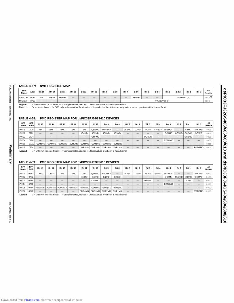
2
01
0 M
icroch
ip T
ech
no
log
y Inc.
Prelim
inary
DS
70
59
1C
-pa
ge
97
ds
PIC
33
FJ
32
GS
40
6/6
06/6
08/6
10 a
nd
ds
PIC
33
FJ
64G
S4
06/6
06/60
8/61
0
TABLE 4-57: NVM REGISTER MAP
TABLE 4-58: PMD REGISTER MAP FOR dsPIC33FJ64GS610 DEVICES
TABLE 4-59: PMD REGISTER MAP FOR dsPIC33FJ32GS610 DEVICES
SFR Name
Addr Bit 15 Bit 14 Bit 13 Bit 12 Bit 11 Bit 10 Bit 9 Bit 8 Bit 7 Bit 6 Bit 5 Bit 4 Bit 3 Bit 2 Bit 1 Bit 0All
Resets
NVMCON 0760 WR WREN WRERR — — — — — — ERASE — — NVMOP<3:0> 0000(1)
NVMKEY 0766 — — — — — — — — NVMKEY<7:0> 0000
Legend: x = unknown value on Reset, — = unimplemented, read as ‘0’. Reset values are shown in hexadecimal.Note 1: Reset value shown is for POR only. Value on other Reset states is dependent on the state of memory write or erase operations at the time of Reset.
SFR Name
SFR Addr
Bit 15 Bit 14 Bit 13 Bit 12 Bit 11 Bit 10 Bit 9 Bit 8 Bit 7 Bit 6 Bit 5 Bit 4 Bit 3 Bit 2 Bit 1 Bit 0All
Resets
PMD1 0770 T5MD T4MD T3MD T2MD T1MD QEI1MD PWMMD — I2C1MD U2MD U1MD SPI2MD SPI1MD — C1MD ADCMD 0000
PMD2 0772 — — — — IC4MD IC3MD IC2MD IC1MD — — — — OC4MD OC3MD OC2MD OC1MD 0000
PMD3 0774 — — — — — CMPMD — — — — QEI2MD — — — I2C2MD — 0000
PMD4 0776 — — — — — — — — — — — — REFOMD — — — 0000
PMD6 077A PWM8MD PWM7MD PWM6MD PWM5MD PWM4MD PWM3MD PWM2MD PWM1MD — — — — — — — — 0000
PMD7 077C — — — — CMP4MD CMP3MD CMP2MD CMP1MD — — — — — — — PWM9MD 0000
Legend: x = unknown value on Reset, — = unimplemented, read as ‘0’. Reset values are shown in hexadecimal.
SFR Name
SFR Addr
Bit 15 Bit 14 Bit 13 Bit 12 Bit 11 Bit 10 Bit 9 Bit 8 Bit 7 Bit 6 Bit 5 Bit 4 Bit 3 Bit 2 Bit 1 Bit 0All
Resets
PMD1 0770 T5MD T4MD T3MD T2MD T1MD QEI1MD PWMMD — I2C1MD U2MD U1MD SPI2MD SPI1MD — — ADCMD 0000
PMD2 0772 — — — — IC4MD IC3MD IC2MD IC1MD — — — — OC4MD OC3MD OC2MD OC1MD 0000
PMD3 0774 — — — — — CMPMD — — — — QEI2MD — — — I2C2MD — 0000
PMD4 0776 — — — — — — — — — — — — REFOMD — — — 0000
PMD6 077A PWM8MD PWM7MD PWM6MD PWM5MD PWM4MD PWM3MD PWM2MD PWM1MD — — — — — — — — 0000
PMD7 077C — — — — CMP4MD CMP3MD CMP2MD CMP1MD — — — — — — — PWM9MD 0000
Legend: x = unknown value on Reset, — = unimplemented, read as ‘0’. Reset values are shown in hexadecimal.
Downloaded from Elcodis.com electronic components distributor

ds
PIC
33
FJ
32
GS
40
6/6
06
/60
8/6
10
an
d d
sP
IC3
3F
J6
4G
S4
06
/60
6/6
08/6
10
DS
70
59
1C
-pa
ge
98
Prelim
ina
ry
20
10
Micro
chip
Te
chn
olo
gy In
c.
TABLE 4-60: PMD REGISTER MAP FOR dsPIC33FJ64GS608 DEVICES
TABLE 4-61: PMD REGISTER MAP FOR dsPIC33FJ32GS608 DEVICES
TABLE 4-62: PMD REGISTER MAP FOR dsPIC33FJ64GS606 DEVICES
SFR Name
SFR Addr
Bit 15 Bit 14 Bit 13 Bit 12 Bit 11 Bit 10 Bit 9 Bit 8 Bit 7 Bit 6 Bit 5 Bit 4 Bit 3 Bit 2 Bit 1 Bit 0All
Resets
PMD1 0770 T5MD T4MD T3MD T2MD T1MD QEI1MD PWMMD — I2C1MD U2MD U1MD SPI2MD SPI1MD — C1MD ADCMD 0000
PMD2 0772 — — — — IC4MD IC3MD IC2MD IC1MD — — — — OC4MD OC3MD OC2MD OC1MD 0000
PMD3 0774 — — — — — CMPMD — — — — QEI2MD — — — I2C2MD — 0000
PMD4 0776 — — — — — — — — — — — — REFOMD — — — 0000
PMD6 077A PWM8MD PWM7MD PWM6MD PWM5MD PWM4MD PWM3MD PWM2MD PWM1MD — — — — — — — — 0000
PMD7 077C — — — — CMP4MD CMP3MD CMP2MD CMP1MD — — — — — — — — 0000
Legend: x = unknown value on Reset, — = unimplemented, read as ‘0’. Reset values are shown in hexadecimal.
SFR Name
SFR Addr
Bit 15 Bit 14 Bit 13 Bit 12 Bit 11 Bit 10 Bit 9 Bit 8 Bit 7 Bit 6 Bit 5 Bit 4 Bit 3 Bit 2 Bit 1 Bit 0All
Resets
PMD1 0770 T5MD T4MD T3MD T2MD T1MD QEI1MD PWMMD — I2C1MD U2MD U1MD SPI2MD SPI1MD — — ADCMD 0000
PMD2 0772 — — — — IC4MD IC3MD IC2MD IC1MD — — — — OC4MD OC3MD OC2MD OC1MD 0000
PMD3 0774 — — — — — CMPMD — — — — QEI2MD — — — I2C2MD — 0000
PMD4 0776 — — — — — — — — — — — — REFOMD — — — 0000
PMD6 077A PWM8MD PWM7MD PWM6MD PWM5MD PWM4MD PWM3MD PWM2MD PWM1MD — — — — — — — — 0000
PMD7 077C — — — — CMP4MD CMP3MD CMP2MD CMP1MD — — — — — — — — 0000
Legend: x = unknown value on Reset, — = unimplemented, read as ‘0’. Reset values are shown in hexadecimal.
SFR Name
SFR Addr
Bit 15 Bit 14 Bit 13 Bit 12 Bit 11 Bit 10 Bit 9 Bit 8 Bit 7 Bit 6 Bit 5 Bit 4 Bit 3 Bit 2 Bit 1 Bit 0All
Resets
PMD1 0770 T5MD T4MD T3MD T2MD T1MD QEI1MD PWMMD — I2C1MD U2MD U1MD SPI2MD SPI1MD — C1MD ADCMD 0000
PMD2 0772 — — — — IC4MD IC3MD IC2MD IC1MD — — — — OC4MD OC3MD OC2MD OC1MD 0000
PMD3 0774 — — — — — CMPMD — — — — QEI2MD — — — I2C2MD — 0000
PMD4 0776 — — — — — — — — — — — — REFOMD — — — 0000
PMD6 077A — — PWM6MD PWM5MD PWM4MD PWM3MD PWM2MD PWM1MD — — — — — — — — 0000
PMD7 077C — — — — CMP4MD CMP3MD CMP2MD CMP1MD — — — — — — — — 0000
Legend: x = unknown value on Reset, — = unimplemented, read as ‘0’. Reset values are shown in hexadecimal.
Downloaded from Elcodis.com electronic components distributor
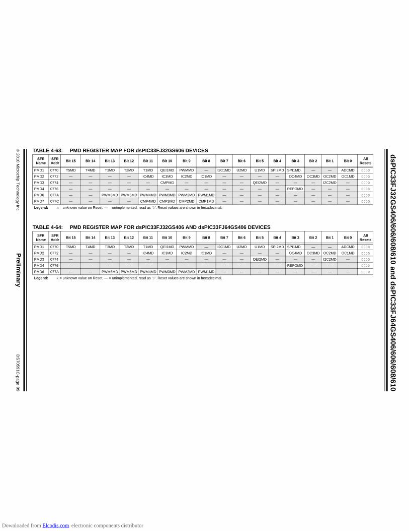
2
01
0 M
icroch
ip T
ech
no
log
y Inc.
Prelim
inary
DS
70
59
1C
-pa
ge
99
ds
PIC
33
FJ
32
GS
40
6/6
06/6
08/6
10 a
nd
ds
PIC
33
FJ
64G
S4
06/6
06/60
8/61
0
TABLE 4-63: PMD REGISTER MAP FOR dsPIC33FJ32GS606 DEVICES
TABLE 4-64: PMD REGISTER MAP FOR dsPIC33FJ32GS406 AND dsPIC33FJ64GS406 DEVICES
SFR Name
SFR Addr
Bit 15 Bit 14 Bit 13 Bit 12 Bit 11 Bit 10 Bit 9 Bit 8 Bit 7 Bit 6 Bit 5 Bit 4 Bit 3 Bit 2 Bit 1 Bit 0All
Resets
PMD1 0770 T5MD T4MD T3MD T2MD T1MD QEI1MD PWMMD — I2C1MD U2MD U1MD SPI2MD SPI1MD — — ADCMD 0000
PMD2 0772 — — — — IC4MD IC3MD IC2MD IC1MD — — — — OC4MD OC3MD OC2MD OC1MD 0000
PMD3 0774 — — — — — CMPMD — — — — QEI2MD — — — I2C2MD — 0000
PMD4 0776 — — — — — — — — — — — — REFOMD — — — 0000
PMD6 077A — — PWM6MD PWM5MD PWM4MD PWM3MD PWM2MD PWM1MD — — — — — — — — 0000
PMD7 077C — — — — CMP4MD CMP3MD CMP2MD CMP1MD — — — — — — — — 0000
Legend: x = unknown value on Reset, — = unimplemented, read as ‘0’. Reset values are shown in hexadecimal.
SFR Name
SFR Addr
Bit 15 Bit 14 Bit 13 Bit 12 Bit 11 Bit 10 Bit 9 Bit 8 Bit 7 Bit 6 Bit 5 Bit 4 Bit 3 Bit 2 Bit 1 Bit 0All
Resets
PMD1 0770 T5MD T4MD T3MD T2MD T1MD QEI1MD PWMMD — I2C1MD U2MD U1MD SPI2MD SPI1MD — — ADCMD 0000
PMD2 0772 — — — — IC4MD IC3MD IC2MD IC1MD — — — — OC4MD OC3MD OC2MD OC1MD 0000
PMD3 0774 — — — — — — — — — — QEI2MD — — — I2C2MD — 0000
PMD4 0776 — — — — — — — — — — — — REFOMD — — — 0000
PMD6 077A — — PWM6MD PWM5MD PWM4MD PWM3MD PWM2MD PWM1MD — — — — — — — — 0000
Legend: x = unknown value on Reset, — = unimplemented, read as ‘0’. Reset values are shown in hexadecimal.
Downloaded from Elcodis.com electronic components distributor

dsPIC33FJ32GS406/606/608/610 and dsPIC33FJ64GS406/606/608/610
DS70591C-page 100 Preliminary 2010 Microchip Technology Inc.
4.2.7 SOFTWARE STACK
In addition to its use as a working register, the W15register in the dsPIC33FJ32GS406/606/608/610 anddsPIC33FJ64GS406/606/608/610 devices is also usedas a software Stack Pointer. The Stack Pointer alwayspoints to the first available free word and grows fromlower to higher addresses. It predecrements for stackpops and post-increments for stack pushes, as shownin Figure 4-6. For a PC push during any CALL instruc-tion, the MSb of the PC is zero-extended before thepush, ensuring that the MSb is always clear.
The Stack Pointer Limit register (SPLIM) associatedwith the Stack Pointer sets an upper address boundaryfor the stack. SPLIM is uninitialized at Reset. As is thecase for the Stack Pointer, SPLIM<0> is forced to ‘0’because all stack operations must be word-aligned.
Whenever an EA is generated using W15 as a sourceor destination pointer, the resulting address iscompared with the value in SPLIM. If the contents ofthe Stack Pointer (W15) and the SPLIM register areequal and a push operation is performed, a stack errortrap will not occur. The stack error trap will occur on asubsequent push operation. For example, to cause astack error trap when the stack grows beyond address0x1800 in RAM, initialize the SPLIM with the value0x17FE.
Similarly, a Stack Pointer underflow (stack error) trap isgenerated when the Stack Pointer address is found tobe less than 0x0800. This prevents the stack frominterfering with the Special Function Register (SFR)space.
A write to the SPLIM register should not be immediatelyfollowed by an indirect read operation using W15.
FIGURE 4-6: CALL STACK FRAME
4.3 Instruction Addressing Modes
The addressing modes shown in Table 4-65 form thebasis of the addressing modes optimized to support thespecific features of individual instructions. Theaddressing modes provided in the MAC class ofinstructions differ from those in the other instructiontypes.
4.3.1 FILE REGISTER INSTRUCTIONS
Most file register instructions use a 13-bit address field(f) to directly address data present in the first 8192bytes of data memory (near data space). Most fileregister instructions employ a working register, W0,which is denoted as WREG in these instructions. Thedestination is typically either the same file register orWREG (with the exception of the MUL instruction),which writes the result to a register or register pair. TheMOV instruction allows additional flexibility and canaccess the entire data space.
4.3.2 MCU INSTRUCTIONS
The three-operand MCU instructions are of the form:
Operand 3 = Operand 1 <function> Operand 2
where Operand 1 is always a working register (that is,the addressing mode can only be register direct), whichis referred to as Wb. Operand 2 can be a W register,fetched from data memory, or a 5-bit literal. The resultlocation can be either a W register or a data memorylocation. The following addressing modes aresupported by MCU instructions:
• Register Direct• Register Indirect• Register Indirect Post-Modified• Register Indirect Pre-Modified• 5-bit or 10-bit Literal
Note: A PC push during exception processingconcatenates the SRL register to the MSbof the PC prior to the push.
<Free Word>
PC<15:0>
000000000
015
W15 (before CALL)
W15 (after CALL)
Sta
ck G
row
s To
wa
rdH
igh
er
Add
ress
0x0000
PC<22:16>
POP : [--W15]PUSH : [W15++]
Note: Not all instructions support all theaddressing modes given above. Individualinstructions can support different subsetsof these addressing modes.
Downloaded from Elcodis.com electronic components distributor

2010 Microchip Technology Inc. Preliminary DS70591C-page 101
dsPIC33FJ32GS406/606/608/610 and dsPIC33FJ64GS406/606/608/610
TABLE 4-65: FUNDAMENTAL ADDRESSING MODES SUPPORTED
4.3.3 MOVE AND ACCUMULATOR INSTRUCTIONS
Move instructions and the DSP accumulator class ofinstructions provide a greater degree of addressingflexibility than other instructions. In addition to theaddressing modes supported by most MCUinstructions, move and accumulator instructions alsosupport Register Indirect with Register OffsetAddressing mode, also referred to as Register Indexedmode.
In summary, the following addressing modes aresupported by move and accumulator instructions:
• Register Direct• Register Indirect• Register Indirect Post-modified• Register Indirect Pre-modified• Register Indirect with Register Offset (Indexed)• Register Indirect with Literal Offset• 8-bit Literal• 16-bit Literal
4.3.4 MAC INSTRUCTIONS
The dual source operand DSP instructions (CLR, ED,EDAC, MAC, MPY, MPY.N, MOVSAC and MSC), also referredto as MAC instructions, use a simplified set of addressingmodes to allow the user application to effectivelymanipulate the data pointers through register indirecttables.
The two-source operand prefetch registers must bemembers of the set {W8, W9, W10, W11}. For datareads, W8 and W9 are always directed to the X RAGU,and W10 and W11 are always directed to the Y AGU.The effective addresses generated (before and aftermodification) must, therefore, be valid addresses withinX data space for W8 and W9 and Y data space for W10and W11.
In summary, the following addressing modes aresupported by the MAC class of instructions:
• Register Indirect• Register Indirect Post-Modified by 2• Register Indirect Post-Modified by 4• Register Indirect Post-Modified by 6• Register Indirect with Register Offset (Indexed)
4.3.5 OTHER INSTRUCTIONS
Besides the addressing modes outlined previously, someinstructions use literal constants of various sizes. Forexample, BRA (branch) instructions use 16-bit signedliterals to specify the branch destination directly, whereasthe DISI instruction uses a 14-bit unsigned literal field. Insome instructions, such as ADD Acc, the source of anoperand or result is implied by the opcode itself. Certainoperations, such as NOP, do not have any operands.
Addressing Mode Description
File Register Direct The address of the file register is specified explicitly.
Register Direct The contents of a register are accessed directly.
Register Indirect The contents of Wn forms the Effective Address (EA).
Register Indirect Post-Modified The contents of Wn forms the EA. Wn is post-modified (incremented or decremented) by a constant value.
Register Indirect Pre-Modified Wn is pre-modified (incremented or decremented) by a signed constant value to form the EA.
Register Indirect with Register Offset (Register Indexed)
The sum of Wn and Wb forms the EA.
Register Indirect with Literal Offset The sum of Wn and a literal forms the EA.
Note: For the MOV instructions, the addressingmode specified in the instruction can differfor the source and destination EA.However, the 4-bit Wb (Register Offset)field is shared by both source anddestination (but typically only used byone).
Note: Not all instructions support all theaddressing modes given above. Individualinstructions may support different subsetsof these addressing modes.
Note: Register Indirect with Register OffsetAddressing mode is available only for W9(in X space) and W11 (in Y space).
Downloaded from Elcodis.com electronic components distributor
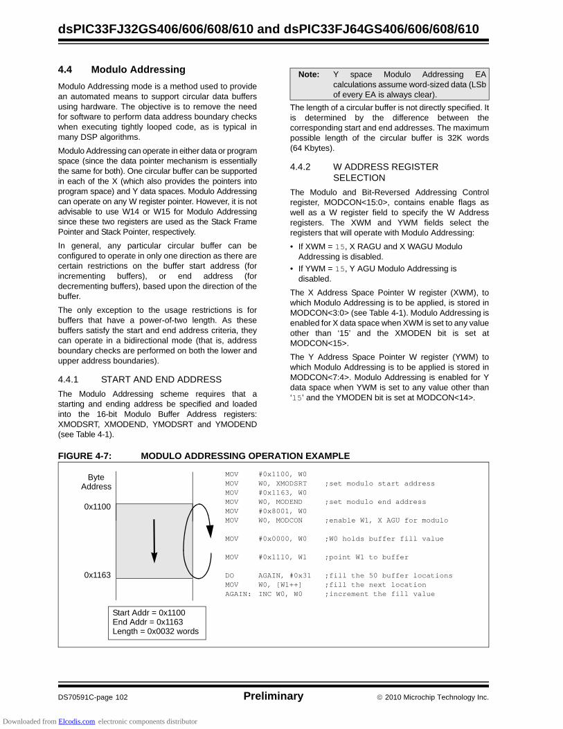
dsPIC33FJ32GS406/606/608/610 and dsPIC33FJ64GS406/606/608/610
DS70591C-page 102 Preliminary 2010 Microchip Technology Inc.
4.4 Modulo Addressing
Modulo Addressing mode is a method used to providean automated means to support circular data buffersusing hardware. The objective is to remove the needfor software to perform data address boundary checkswhen executing tightly looped code, as is typical inmany DSP algorithms.
Modulo Addressing can operate in either data or programspace (since the data pointer mechanism is essentiallythe same for both). One circular buffer can be supportedin each of the X (which also provides the pointers intoprogram space) and Y data spaces. Modulo Addressingcan operate on any W register pointer. However, it is notadvisable to use W14 or W15 for Modulo Addressingsince these two registers are used as the Stack FramePointer and Stack Pointer, respectively.
In general, any particular circular buffer can beconfigured to operate in only one direction as there arecertain restrictions on the buffer start address (forincrementing buffers), or end address (fordecrementing buffers), based upon the direction of thebuffer.
The only exception to the usage restrictions is forbuffers that have a power-of-two length. As thesebuffers satisfy the start and end address criteria, theycan operate in a bidirectional mode (that is, addressboundary checks are performed on both the lower andupper address boundaries).
4.4.1 START AND END ADDRESS
The Modulo Addressing scheme requires that astarting and ending address be specified and loadedinto the 16-bit Modulo Buffer Address registers:XMODSRT, XMODEND, YMODSRT and YMODEND(see Table 4-1).
The length of a circular buffer is not directly specified. Itis determined by the difference between thecorresponding start and end addresses. The maximumpossible length of the circular buffer is 32K words(64 Kbytes).
4.4.2 W ADDRESS REGISTER SELECTION
The Modulo and Bit-Reversed Addressing Controlregister, MODCON<15:0>, contains enable flags aswell as a W register field to specify the W Addressregisters. The XWM and YWM fields select theregisters that will operate with Modulo Addressing:
• If XWM = 15, X RAGU and X WAGU Modulo Addressing is disabled.
• If YWM = 15, Y AGU Modulo Addressing is disabled.
The X Address Space Pointer W register (XWM), towhich Modulo Addressing is to be applied, is stored inMODCON<3:0> (see Table 4-1). Modulo Addressing isenabled for X data space when XWM is set to any valueother than ‘15’ and the XMODEN bit is set atMODCON<15>.
The Y Address Space Pointer W register (YWM) towhich Modulo Addressing is to be applied is stored inMODCON<7:4>. Modulo Addressing is enabled for Ydata space when YWM is set to any value other than‘15’ and the YMODEN bit is set at MODCON<14>.
FIGURE 4-7: MODULO ADDRESSING OPERATION EXAMPLE
Note: Y space Modulo Addressing EAcalculations assume word-sized data (LSbof every EA is always clear).
0x1100
0x1163
Start Addr = 0x1100End Addr = 0x1163Length = 0x0032 words
ByteAddress
MOV #0x1100, W0MOV W0, XMODSRT ;set modulo start addressMOV #0x1163, W0MOV W0, MODEND ;set modulo end addressMOV #0x8001, W0MOV W0, MODCON ;enable W1, X AGU for modulo
MOV #0x0000, W0 ;W0 holds buffer fill value
MOV #0x1110, W1 ;point W1 to buffer
DO AGAIN, #0x31 ;fill the 50 buffer locationsMOV W0, [W1++] ;fill the next locationAGAIN: INC W0, W0 ;increment the fill value
Downloaded from Elcodis.com electronic components distributor
2010 Microchip Technology Inc. Preliminary DS70591C-page 103
dsPIC33FJ32GS406/606/608/610 and dsPIC33FJ64GS406/606/608/610
4.4.3 MODULO ADDRESSING APPLICABILITY
Modulo Addressing can be applied to the EffectiveAddress (EA) calculation associated with any Wregister. Address boundaries check for addressesequal to:
• The upper boundary addresses for incrementing buffers
• The lower boundary addresses for decrementing buffers
It is important to realize that the address boundariescheck for addresses less than or greater than the upper(for incrementing buffers) and lower (for decrementingbuffers) boundary addresses (not just equal to).Address changes can, therefore, jump beyondboundaries and still be adjusted correctly.
4.5 Bit-Reversed Addressing
Bit-Reversed Addressing mode is intended to simplifydata re-ordering for radix-2 FFT algorithms. It issupported by the X AGU for data writes only.
The modifier, which can be a constant value or registercontents, is regarded as having its bit order reversed. Theaddress source and destination are kept in normal order.Thus, the only operand requiring reversal is the modifier.
4.5.1 BIT-REVERSED ADDRESSING IMPLEMENTATION
Bit-Reversed Addressing mode is enabled in any ofthese situations:
• BWM bits (W register selection) in the MODCON register are any value other than ‘15’ (the stack cannot be accessed using Bit-Reversed Addressing)
• The BREN bit is set in the XBREV register
• The addressing mode used is Register Indirect with Pre-Increment or Post-Increment
If the length of a bit-reversed buffer is M = 2N bytes,the last ‘N’ bits of the data buffer start address mustbe zeros.
XB<14:0> is the Bit-Reversed Address modifier, or‘pivot point,’ which is typically a constant. In the case ofan FFT computation, its value is equal to half of the FFTdata buffer size.
When enabled, Bit-Reversed Addressing is executedonly for Register Indirect with Pre-Increment orPost-Increment Addressing and word-sized datawrites. It will not function for any other addressingmode or for byte-sized data, and normal addresses aregenerated instead. When Bit-Reversed Addressing isactive, the W Address Pointer is always added to theaddress modifier (XB), and the offset associated withthe Register Indirect Addressing mode is ignored. Inaddition, as word-sized data is a requirement, the LSbof the EA is ignored (and always clear).
If Bit-Reversed Addressing has already been enabledby setting the BREN (XBREV<15>) bit, a write to theXBREV register should not be immediately followed byan indirect read operation using the W register that hasbeen designated as the bit-reversed pointer.
Note: The modulo corrected effective address iswritten back to the register only whenPre-Modify or Post-Modify Addressingmode is used to compute the effectiveaddress. When an address offset (such as[W7 + W2]) is used, Modulo Addresscorrection is performed but the contents ofthe register remain unchanged.
Note: All bit-reversed EA calculations assumeword-sized data (LSb of every EA isalways clear). The XB value is scaledaccordingly to generate compatible (byte)addresses.
Note: Modulo Addressing and Bit-ReversedAddressing should not be enabledtogether. If an application attempts to do so,Bit-Reversed Addressing will assumepriority when active for the X WAGU and XWAGU, Modulo Addressing will be dis-abled. However, Modulo Addressing willcontinue to function in the X RAGU.
Downloaded from Elcodis.com electronic components distributor
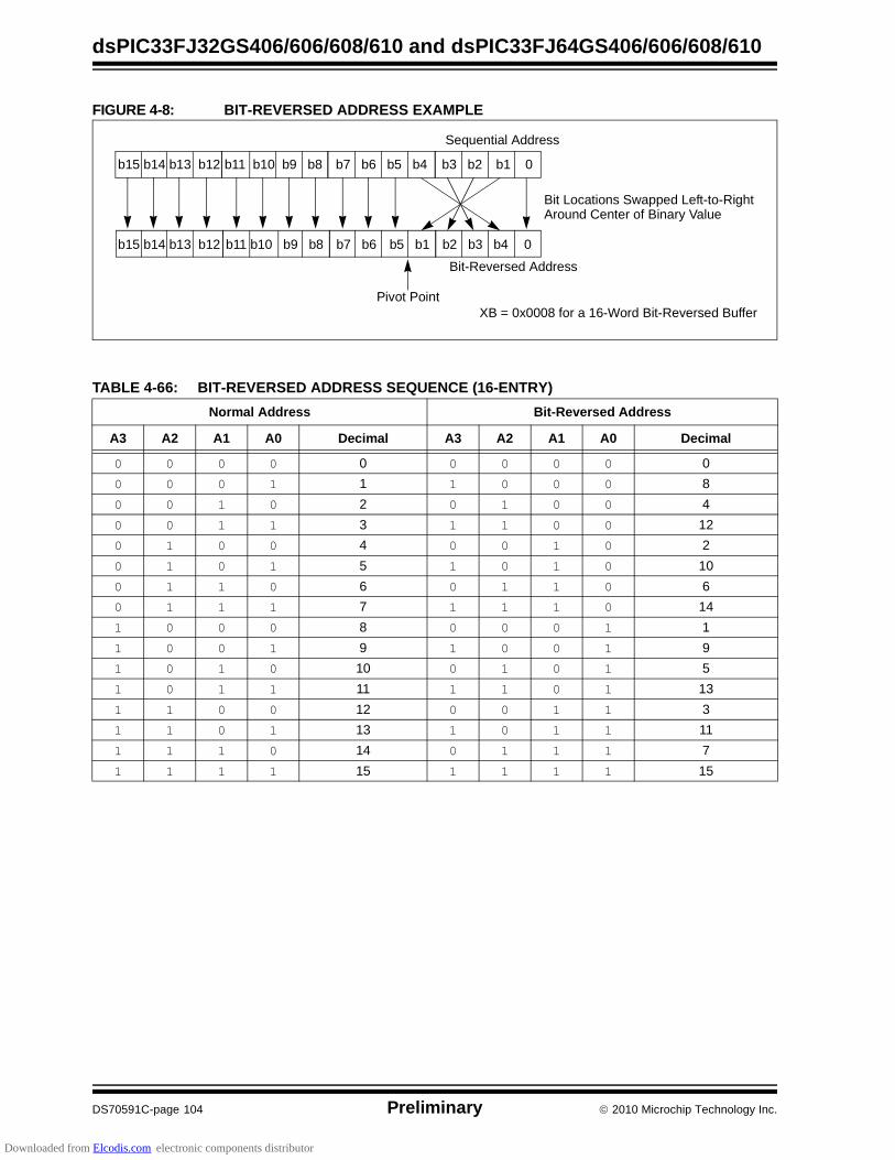
dsPIC33FJ32GS406/606/608/610 and dsPIC33FJ64GS406/606/608/610
DS70591C-page 104 Preliminary 2010 Microchip Technology Inc.
FIGURE 4-8: BIT-REVERSED ADDRESS EXAMPLE
TABLE 4-66: BIT-REVERSED ADDRESS SEQUENCE (16-ENTRY)
b3 b2 b1 0
b2 b3 b4 0
Bit Locations Swapped Left-to-RightAround Center of Binary Value
Bit-Reversed Address
XB = 0x0008 for a 16-Word Bit-Reversed Buffer
b7 b6 b5 b1
b7 b6 b5 b4b11 b10 b9 b8
b11 b10 b9 b8
b15 b14 b13 b12
b15 b14 b13 b12
Sequential Address
Pivot Point
Normal Address Bit-Reversed Address
A3 A2 A1 A0 Decimal A3 A2 A1 A0 Decimal
0 0 0 0 0 0 0 0 0 0
0 0 0 1 1 1 0 0 0 8
0 0 1 0 2 0 1 0 0 4
0 0 1 1 3 1 1 0 0 12
0 1 0 0 4 0 0 1 0 2
0 1 0 1 5 1 0 1 0 10
0 1 1 0 6 0 1 1 0 6
0 1 1 1 7 1 1 1 0 14
1 0 0 0 8 0 0 0 1 1
1 0 0 1 9 1 0 0 1 9
1 0 1 0 10 0 1 0 1 5
1 0 1 1 11 1 1 0 1 13
1 1 0 0 12 0 0 1 1 3
1 1 0 1 13 1 0 1 1 11
1 1 1 0 14 0 1 1 1 7
1 1 1 1 15 1 1 1 1 15
Downloaded from Elcodis.com electronic components distributor

2010 Microchip Technology Inc. Preliminary DS70591C-page 105
dsPIC33FJ32GS406/606/608/610 and dsPIC33FJ64GS406/606/608/610
4.6 Interfacing Program and Data Memory Spaces
The dsPIC33FJ32GS406/606/608/610 anddsPIC33FJ64GS406/606/608/610 architecture uses a24-bit-wide program space and a 16-bit-wide data space.The architecture is also a modified Harvard scheme,meaning that data can also be present in the programspace. To use this data successfully, it must be accessedin a way that preserves the alignment of information inboth spaces.
Aside from normal execution, thedsPIC33FJ32GS406/606/608/610 anddsPIC33FJ64GS406/606/608/610 architectureprovides two methods by which program space can beaccessed during operation:
• Using table instructions to access individual bytes or words anywhere in the program space
• Remapping a portion of the program space into the data space (Program Space Visibility)
Table instructions allow an application to read or writeto small areas of the program memory. This capabilitymakes the method ideal for accessing data tables thatneed to be updated periodically. It also allows accessto all bytes of the program word. The remappingmethod allows an application to access a large block ofdata on a read-only basis, which is ideal for look-upsfrom a large table of static data. The application canonly access the least significant word of the programword.
4.6.1 ADDRESSING PROGRAM SPACE
Since the address ranges for the data and programspaces are 16 and 24 bits, respectively, a method isneeded to create a 23-bit or 24-bit program addressfrom 16-bit data registers. The solution depends on theinterface method to be used.
For table operations, the 8-bit Table Page register(TBLPAG) is used to define a 32K word region withinthe program space. This is concatenated with a 16-bitEA to arrive at a full 24-bit program space address. Inthis format, the Most Significant bit of TBLPAG is usedto determine if the operation occurs in the user memory(TBLPAG<7> = 0) or the configuration memory(TBLPAG<7> = 1).
For remapping operations, the 8-bit Program SpaceVisibility Register (PSVPAG) is used to define a16K word page in the program space. When the MostSignificant bit of the EA is ‘1’, PSVPAG is concatenatedwith the lower 15 bits of the EA to form a 23-bit programspace address. Unlike table operations, this limitsremapping operations strictly to the user memory area.
Table 4-67 and Figure 4-9 show how the program EA iscreated for table operations and remapping accessesfrom the data EA. Here, P<23:0> refers to a programspace word, and D<15:0> refers to a data space word.
TABLE 4-67: PROGRAM SPACE ADDRESS CONSTRUCTION
Access TypeAccessSpace
Program Space Address
<23> <22:16> <15> <14:1> <0>
Instruction Access(Code Execution)
User 0 PC<22:1> 0
0xx xxxx xxxx xxxx xxxx xxx0
TBLRD/TBLWT(Byte/Word Read/Write)
User TBLPAG<7:0> Data EA<15:0>
0xxx xxxx xxxx xxxx xxxx xxxx
Configuration TBLPAG<7:0> Data EA<15:0>
1xxx xxxx xxxx xxxx xxxx xxxx
Program Space Visibility(Block Remap/Read)
User 0 PSVPAG<7:0> Data EA<14:0>(1)
0 xxxx xxxx xxx xxxx xxxx xxxx
Note 1: Data EA<15> is always ‘1’ in this case, but is not used in calculating the program space address. Bit 15 of the address is PSVPAG<0>.
Downloaded from Elcodis.com electronic components distributor

dsPIC33FJ32GS406/606/608/610 and dsPIC33FJ64GS406/606/608/610
DS70591C-page 106 Preliminary 2010 Microchip Technology Inc.
FIGURE 4-9: DATA ACCESS FROM PROGRAM SPACE ADDRESS GENERATION
0Program Counter
23 bits
1
PSVPAG
8 bits
EA
15 bits
Program Counter(1)
Select
TBLPAG
8 bits
EA
16 bits
Byte Select
0
0
1/0
User/Configuration
Table Operations(2)
Program Space Visibility(1)
Space Select
24 bits
23 bits
(Remapping)
1/0
0
Note 1: The Least Significant bit (LSb) of program space addresses is always fixed as ‘0’ to maintain wordalignment of data in the program and data spaces.
2: Table operations are not required to be word-aligned. Table read operations are permitted in theconfiguration memory space.
Downloaded from Elcodis.com electronic components distributor

2010 Microchip Technology Inc. Preliminary DS70591C-page 107
dsPIC33FJ32GS406/606/608/610 and dsPIC33FJ64GS406/606/608/610
4.6.2 DATA ACCESS FROM PROGRAM MEMORY USING TABLE INSTRUCTIONS
The TBLRDL and TBLWTL instructions offer a directmethod of reading or writing the lower word of anyaddress within the program space without goingthrough data space. The TBLRDH and TBLWTHinstructions are the only method to read or write theupper 8 bits of a program space word as data.
The PC is incremented by two for each successive24-bit program word. This allows program memoryaddresses to directly map to data space addresses.Program memory can thus be regarded as two16-bit-wide word address spaces, residing side by side,each with the same address range. TBLRDL andTBLWTL access the space that contains the leastsignificant data word. TBLRDH and TBLWTH access thespace that contains the upper data byte.
Two table instructions are provided to move byte orword-sized (16-bit) data to and from program space.Both function as either byte or word operations.
• TBLRDL (Table Read Low):
- In Word mode, this instruction maps the lower word of the program space location (P<15:0>) to a data address (D<15:0>).
- In Byte mode, either the upper or lower byte of the lower program word is mapped to the lower byte of a data address. The upper byte is selected when Byte Select is ‘1’; the lower byte is selected when it is ‘0’.
• TBLRDH (Table Read High):
- In Word mode, this instruction maps the entire upper word of a program address (P<23:16>) to a data address. Note that D<15:8>, the ‘phantom byte’, will always be ‘0’.
- In Byte mode, this instruction maps the upper or lower byte of the program word to D<7:0> of the data address, in the TBLRDL instruction. The data is always ‘0’ when the upper ‘phantom’ byte is selected (Byte Select = 1).
Similarly, two table instructions, TBLWTH and TBLWTL,are used to write individual bytes or words to a programspace address. The details of their operation areexplained in Section 5.0 “Flash Program Memory”.
For all table operations, the area of program memoryspace to be accessed is determined by the Table Pageregister (TBLPAG). TBLPAG covers the entire programmemory space of the device, including user andconfiguration spaces. When TBLPAG<7> = 0, the tablepage is located in the user memory space. WhenTBLPAG<7> = 1, the page is located in configurationspace.
FIGURE 4-10: ACCESSING PROGRAM MEMORY WITH TABLE INSTRUCTIONS
081623
00000000
00000000
00000000
00000000
‘Phantom’ Byte
TBLRDH.B (Wn<0> = 0)
TBLRDL.W
TBLRDL.B (Wn<0> = 1)
TBLRDL.B (Wn<0> = 0)
23 15 0
TBLPAG
02
0x000000
0x800000
0x020000
0x030000
Program Space
The address for the table operation is determined by the data EAwithin the page defined by the TBLPAG register. Only read operations are shown; write operations are also valid inthe user memory area.
Downloaded from Elcodis.com electronic components distributor

dsPIC33FJ32GS406/606/608/610 and dsPIC33FJ64GS406/606/608/610
DS70591C-page 108 Preliminary 2010 Microchip Technology Inc.
4.6.3 READING DATA FROM PROGRAM MEMORY USING PROGRAM SPACE VISIBILITY
The upper 32 Kbytes of data space may optionally bemapped into any 16K word page of the program space.This option provides transparent access to storedconstant data from the data space without the need touse special instructions (such as TBLRDL/H).
Program space access through the data space occursif the Most Significant bit of the data space EA is ‘1’ andprogram space visibility is enabled by setting the PSVbit in the Core Control register (CORCON<2>). Thelocation of the program memory space to be mappedinto the data space is determined by the ProgramSpace Visibility Page register (PSVPAG). This 8-bitregister defines any one of 256 possible pages of16K words in program space. In effect, PSVPAGfunctions as the upper 8 bits of the program memoryaddress, with the 15 bits of the EA functioning as thelower bits. By incrementing the PC by 2 for eachprogram memory word, the lower 15 bits of data spaceaddresses directly map to the lower 15 bits in thecorresponding program space addresses.
Data reads to this area add a cycle to the instructionbeing executed, since two program memory fetchesare required.
Although each data space address 8000h and highermaps directly into a corresponding program memoryaddress (see Figure 4-11), only the lower 16 bits of the
24-bit program word are used to contain the data. Theupper 8 bits of any program space location used asdata should be programmed with ‘1111 1111’ or‘0000 0000’ to force a NOP. This prevents possibleissues should the area of code ever be accidentallyexecuted.
For operations that use PSV and are executed outsidea REPEAT loop, the MOV and MOV.D instructions requireone instruction cycle in addition to the specifiedexecution time. All other instructions require twoinstruction cycles in addition to the specified executiontime.
For operations that use PSV, and are executed insidea REPEAT loop, these instances require two instructioncycles in addition to the specified execution time of theinstruction:
• Execution in the first iteration
• Execution in the last iteration
• Execution prior to exiting the loop due to an interrupt
• Execution upon re-entering the loop after an interrupt is serviced
Any other iteration of the REPEAT loop will allow theinstruction using PSV to access data, to execute in asingle cycle.
FIGURE 4-11: PROGRAM SPACE VISIBILITY OPERATION
Note: PSV access is temporarily disabled duringtable reads/writes.
23 15 0PSVPAGData SpaceProgram Space
0x0000
0x8000
0xFFFF
020x000000
0x800000
0x010000
0x018000
When CORCON<2> = 1 and EA<15> = 1:
The data in the page designated by PSVPAG is mapped into the upper half of the data memory space...
Data EA<14:0>
...while the lower 15 bits of the EA specify an exact address within the PSV area. This corresponds exactly to the same lower 15 bits of the actual program space address.
PSV Area
Downloaded from Elcodis.com electronic components distributor
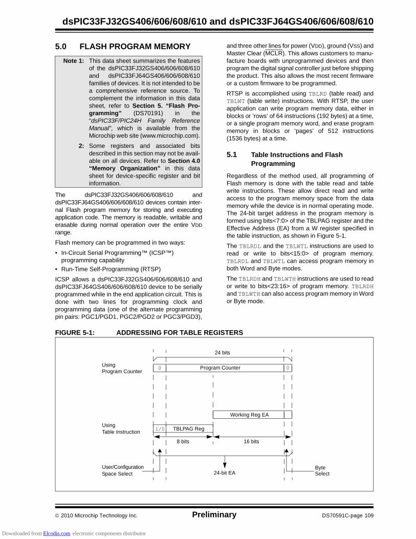
2010 Microchip Technology Inc. Preliminary DS70591C-page 109
dsPIC33FJ32GS406/606/608/610 and dsPIC33FJ64GS406/606/608/610
5.0 FLASH PROGRAM MEMORY
The dsPIC33FJ32GS406/606/608/610 anddsPIC33FJ64GS406/606/608/610 devices contain inter-nal Flash program memory for storing and executingapplication code. The memory is readable, writable anderasable during normal operation over the entire VDD
range.
Flash memory can be programmed in two ways:
• In-Circuit Serial Programming™ (ICSP™) programming capability
• Run-Time Self-Programming (RTSP)
ICSP allows a dsPIC33FJ32GS406/606/608/610 anddsPIC33FJ64GS406/606/608/610 device to be seriallyprogrammed while in the end application circuit. This isdone with two lines for programming clock andprogramming data (one of the alternate programmingpin pairs: PGC1/PGD1, PGC2/PGD2 or PGC3/PGD3),
and three other lines for power (VDD), ground (VSS) andMaster Clear (MCLR). This allows customers to manu-facture boards with unprogrammed devices and thenprogram the digital signal controller just before shippingthe product. This also allows the most recent firmwareor a custom firmware to be programmed.
RTSP is accomplished using TBLRD (table read) andTBLWT (table write) instructions. With RTSP, the userapplication can write program memory data, either inblocks or ‘rows’ of 64 instructions (192 bytes) at a time,or a single program memory word, and erase programmemory in blocks or ‘pages’ of 512 instructions(1536 bytes) at a time.
5.1 Table Instructions and Flash Programming
Regardless of the method used, all programming ofFlash memory is done with the table read and tablewrite instructions. These allow direct read and writeaccess to the program memory space from the datamemory while the device is in normal operating mode.The 24-bit target address in the program memory isformed using bits<7:0> of the TBLPAG register and theEffective Address (EA) from a W register specified inthe table instruction, as shown in Figure 5-1.
The TBLRDL and the TBLWTL instructions are used toread or write to bits<15:0> of program memory.TBLRDL and TBLWTL can access program memory inboth Word and Byte modes.
The TBLRDH and TBLWTH instructions are used to reador write to bits<23:16> of program memory. TBLRDHand TBLWTH can also access program memory in Wordor Byte mode.
FIGURE 5-1: ADDRESSING FOR TABLE REGISTERS
Note 1: This data sheet summarizes the featuresof the dsPIC33FJ32GS406/606/608/610and dsPIC33FJ64GS406/606/608/610families of devices. It is not intended to bea comprehensive reference source. Tocomplement the information in this datasheet, refer to Section 5. “Flash Pro-gramming” (DS70191) in the“dsPIC33F/PIC24H Family ReferenceManual”, which is available from theMicrochip web site (www.microchip.com).
2: Some registers and associated bitsdescribed in this section may not be avail-able on all devices. Refer to Section 4.0“Memory Organization” in this datasheet for device-specific register and bitinformation.
0Program Counter
24 bits
Program Counter
TBLPAG Reg
8 bits
Working Reg EA
16 bits
Byte24-bit EA
0
1/0
Select
UsingTable Instruction
Using
User/ConfigurationSpace Select
Downloaded from Elcodis.com electronic components distributor

dsPIC33FJ32GS406/606/608/610 and dsPIC33FJ64GS406/606/608/610
DS70591C-page 110 Preliminary 2010 Microchip Technology Inc.
5.2 RTSP Operation
The dsPIC33FJ32GS406/606/608/610 anddsPIC33FJ64GS406/606/608/610 Flash program mem-ory array is organized into rows of 64 instructions or 192bytes. RTSP allows the user application to erase a pageof memory, which consists of eight rows (512 instruc-tions) at a time, and to program one row or one word at atime. Table 27-12 shows typical erase and programmingtimes. The 8-row erase pages and single row write rowsare edge-aligned from the beginning of program memory,on boundaries of 1536 bytes and 192 bytes, respectively.
The program memory implements holding buffers thatcan contain 64 instructions of programming data. Priorto the actual programming operation, the write datamust be loaded into the buffers sequentially. Theinstruction words loaded must always be from a groupof 64 boundary.
The basic sequence for RTSP programming is to set upa Table Pointer, then do a series of TBLWT instructionsto load the buffers. Programming is performed bysetting the control bits in the NVMCON register. A totalof 64 TBLWTL and TBLWTH instructions are requiredto load the instructions.
All of the table write operations are single-word writes(two instruction cycles) because only the buffers arewritten. A programming cycle is required forprogramming each row.
5.3 Programming Operations
A complete programming sequence is necessary forprogramming or erasing the internal Flash in RTSPmode. The processor stalls (waits) until theprogramming operation is finished.
The programming time depends on the FRC accuracy(see Table 27-20) and the value of the FRC OscillatorTuning register (see Register 9-4). Use the followingformula to calculate the minimum and maximum valuesfor the Row Write Time, Page Erase Time, and WordWrite Cycle Time parameters (see Table 27-12).
EQUATION 5-1: PROGRAMMING TIME
For example, if the device is operating at +125°C,the FRC accuracy will be ±5%. If the TUN<5:0> bits(see Register 9-4) are set to ‘b000000, theMinimum Row Write Time is:
and, the Maximum Row Write Time is:
Setting the WR bit (NVMCON<15>) starts the opera-tion, and the WR bit is automatically cleared when theoperation is finished.
5.4 Control Registers
Two SFRs are used to read and write the programFlash memory: NVMCON and NVMKEY.
The NVMCON register (Register 5-1) controls whichblocks are to be erased, which memory type is to beprogrammed and the start of the programming cycle.
NVMKEY is a write-only register that is used for writeprotection. To start a programming or erase sequence,the user application must consecutively write 0x55 and0xAA to the NVMKEY register. Refer to Section 5.3“Programming Operations” for further details.
T7.37 MHz FRC Accuracy % FRC Tuning %--------------------------------------------------------------------------------------------------------------------------
TRW11064 Cycles
7.37 MHz 1 0.05+ 1 0– ------------------------------------------------------------------------------ 1.43ms==
TRW11064 Cycles
7.37 MHz 1 0.05– 1 0– ----------------------------------------------------------------------------- 1.58ms==
Downloaded from Elcodis.com electronic components distributor

2010 Microchip Technology Inc. Preliminary DS70591C-page 111
dsPIC33FJ32GS406/606/608/610 and dsPIC33FJ64GS406/606/608/610
REGISTER 5-1: NVMCON: FLASH MEMORY CONTROL REGISTER
R/SO-0(1) R/W-0(1) R/W-0(1) U-0 U-0 U-0 U-0 U-0
WR WREN WRERR — — — — —
bit 15 bit 8
U-0 R/W-0(1) U-0 U-0 R/W-0(1) R/W-0(1) R/W-0(1) R/W-0(1)
— ERASE — — NVMOP<3:0>(2)
bit 7 bit 0
Legend: SO = Settable Only bit
R = Readable bit W = Writable bit U = Unimplemented bit, read as ‘0’
-n = Value at POR ‘1’ = Bit is set ‘0’ = Bit is cleared x = Bit is unknown
bit 15 WR: Write Control bit
1 = Initiates a Flash memory program or erase operation. The operation is self-timed and the bit iscleared by hardware once operation is complete.
0 = Program or erase operation is complete and inactive
bit 14 WREN: Write Enable bit
1 = Enable Flash program/erase operations0 = Inhibit Flash program/erase operations
bit 13 WRERR: Write Sequence Error Flag bit
1 = An improper program or erase sequence attempt or termination has occurred (bit is setautomatically on any set attempt of the WR bit)
0 = The program or erase operation completed normally
bit 12-7 Unimplemented: Read as ‘0’
bit 6 ERASE: Erase/Program Enable bit
1 = Perform the erase operation specified by NVMOP<3:0> on the next WR command0 = Perform the program operation specified by NVMOP<3:0> on the next WR command
bit 5-4 Unimplemented: Read as ‘0’
bit 3-0 NVMOP<3:0>: NVM Operation Select bits(2)
If ERASE = 1:1111 = Memory bulk erase operation1101 = Erase general segment0011 = No operation0010 = Memory page erase operation0001 = No operation0000 = Erase a single Configuration register byte
If ERASE = 0:1111 = No operation1101 = No operation0011 = Memory word program operation0010 = No operation0001 = Memory row program operation0000 = Program a single Configuration register byte
Note 1: These bits can only be Reset on POR.
2: All other combinations of NVMOP<3:0> are unimplemented.
Downloaded from Elcodis.com electronic components distributor
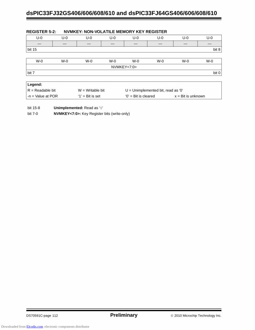
dsPIC33FJ32GS406/606/608/610 and dsPIC33FJ64GS406/606/608/610
DS70591C-page 112 Preliminary 2010 Microchip Technology Inc.
REGISTER 5-2: NVMKEY: NON-VOLATILE MEMORY KEY REGISTER
U-0 U-0 U-0 U-0 U-0 U-0 U-0 U-0
— — — — — — — —
bit 15 bit 8
W-0 W-0 W-0 W-0 W-0 W-0 W-0 W-0
NVMKEY<7:0>
bit 7 bit 0
Legend:
R = Readable bit W = Writable bit U = Unimplemented bit, read as ‘0’
-n = Value at POR ‘1’ = Bit is set ‘0’ = Bit is cleared x = Bit is unknown
bit 15-8 Unimplemented: Read as ‘0’
bit 7-0 NVMKEY<7:0>: Key Register bits (write-only)
Downloaded from Elcodis.com electronic components distributor

2010 Microchip Technology Inc. Preliminary DS70591C-page 113
dsPIC33FJ32GS406/606/608/610 and dsPIC33FJ64GS406/606/608/610
5.4.1 PROGRAMMING ALGORITHM FOR FLASH PROGRAM MEMORY
One row of program Flash memory can beprogrammed at a time. To achieve this, it is necessaryto erase the 8-row erase page that contains the desiredrow. The general process is:
1. Read eight rows of program memory(512 instructions) and store in data RAM.
2. Update the program data in RAM with thedesired new data.
3. Erase the block (see Example 5-1):
a) Set the NVMOP bits (NVMCON<3:0>) to‘0010’ to configure for block erase. Set theERASE (NVMCON<6>) and WREN(NVMCON<14>) bits.
b) Write the starting address of the page to beerased into the TBLPAG and W registers.
c) Write 0x55 to NVMKEY.
d) Write 0xAA to NVMKEY.
e) Set the WR bit (NVMCON<15>). The erasecycle begins and the CPU stalls for theduration of the erase cycle. When the erase isdone, the WR bit is cleared automatically.
4. Write the first 64 instructions from data RAM intothe program memory buffers (see Example 5-2).
5. Write the program block to Flash memory:
a) Set the NVMOP bits to ‘0001’ to configurefor row programming. Clear the ERASE bitand set the WREN bit.
b) Write 0x55 to NVMKEY.
c) Write 0xAA to NVMKEY.
d) Set the WR bit. The programming cyclebegins and the CPU stalls for the duration ofthe write cycle. When the write to Flashmemory is done, the WR bit is clearedautomatically.
6. Repeat steps 4 and 5, using the next available64 instructions from the block in data RAM byincrementing the value in TBLPAG, until all512 instructions are written back to Flash memory.
For protection against accidental operations, the writeinitiate sequence for NVMKEY must be used to allowany erase or program operation to proceed. After theprogramming command has been executed, the userapplication must wait for the programming time untilprogramming is complete. The two instructionsfollowing the start of the programming sequenceshould be NOPs, as shown in Example 5-3.
EXAMPLE 5-1: ERASING A PROGRAM MEMORY PAGE
; Set up NVMCON for block erase operationMOV #0x4042, W0 ;MOV W0, NVMCON ; Initialize NVMCON
; Init pointer to row to be ERASEDMOV #tblpage(PROG_ADDR), W0 ; MOV W0, TBLPAG ; Initialize PM Page Boundary SFRMOV #tbloffset(PROG_ADDR), W0 ; Initialize in-page EA[15:0] pointerTBLWTL W0, [W0] ; Set base address of erase blockDISI #5 ; Block all interrupts with priority <7
; for next 5 instructionsMOV #0x55, W0 MOV W0, NVMKEY ; Write the 55 key MOV #0xAA, W1 ;MOV W1, NVMKEY ; Write the AA keyBSET NVMCON, #WR ; Start the erase sequence NOP ; Insert two NOPs after the eraseNOP ; command is asserted
Downloaded from Elcodis.com electronic components distributor
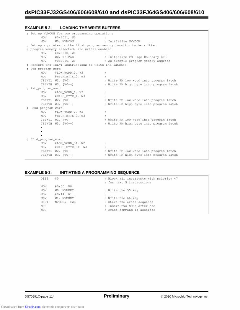
dsPIC33FJ32GS406/606/608/610 and dsPIC33FJ64GS406/606/608/610
DS70591C-page 114 Preliminary 2010 Microchip Technology Inc.
EXAMPLE 5-2: LOADING THE WRITE BUFFERS
EXAMPLE 5-3: INITIATING A PROGRAMMING SEQUENCE
; Set up NVMCON for row programming operationsMOV #0x4001, W0 ;MOV W0, NVMCON ; Initialize NVMCON
; Set up a pointer to the first program memory location to be written; program memory selected, and writes enabled
MOV #0x0000, W0 ; MOV W0, TBLPAG ; Initialize PM Page Boundary SFRMOV #0x6000, W0 ; An example program memory address
; Perform the TBLWT instructions to write the latches; 0th_program_word
MOV #LOW_WORD_0, W2 ; MOV #HIGH_BYTE_0, W3 ; TBLWTL W2, [W0] ; Write PM low word into program latchTBLWTH W3, [W0++] ; Write PM high byte into program latch
; 1st_program_wordMOV #LOW_WORD_1, W2 ; MOV #HIGH_BYTE_1, W3 ; TBLWTL W2, [W0] ; Write PM low word into program latchTBLWTH W3, [W0++] ; Write PM high byte into program latch
; 2nd_program_wordMOV #LOW_WORD_2, W2 ; MOV #HIGH_BYTE_2, W3 ; TBLWTL W2, [W0] ; Write PM low word into program latchTBLWTH W3, [W0++] ; Write PM high byte into program latch•••
; 63rd_program_wordMOV #LOW_WORD_31, W2 ; MOV #HIGH_BYTE_31, W3 ; TBLWTL W2, [W0] ; Write PM low word into program latchTBLWTH W3, [W0++] ; Write PM high byte into program latch
DISI #5 ; Block all interrupts with priority <7; for next 5 instructions
MOV #0x55, W0MOV W0, NVMKEY ; Write the 55 key MOV #0xAA, W1 ;MOV W1, NVMKEY ; Write the AA keyBSET NVMCON, #WR ; Start the erase sequence NOP ; Insert two NOPs after theNOP ; erase command is asserted
Downloaded from Elcodis.com electronic components distributor
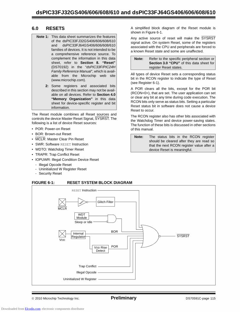
2010 Microchip Technology Inc. Preliminary DS70591C-page 115
dsPIC33FJ32GS406/606/608/610 and dsPIC33FJ64GS406/606/608/610
6.0 RESETS
The Reset module combines all Reset sources andcontrols the device Master Reset Signal, SYSRST. Thefollowing is a list of device Reset sources:
• POR: Power-on Reset
• BOR: Brown-out Reset
• MCLR: Master Clear Pin Reset
• SWR: Software RESET Instruction
• WDTO: Watchdog Timer Reset
• TRAPR: Trap Conflict Reset
• IOPUWR: Illegal Condition Device Reset
- Illegal Opcode Reset- Uninitialized W Register Reset- Security Reset
A simplified block diagram of the Reset module isshown in Figure 6-1.
Any active source of reset will make the SYSRSTsignal active. On system Reset, some of the registersassociated with the CPU and peripherals are forced toa known Reset state and some are unaffected.
All types of device Reset sets a corresponding statusbit in the RCON register to indicate the type of Reset(see Register 6-1).
A POR clears all the bits, except for the POR bit(RCON<0>), that are set. The user application can setor clear any bit at any time during code execution. TheRCON bits only serve as status bits. Setting a particularReset status bit in software does not cause a deviceReset to occur.
The RCON register also has other bits associated withthe Watchdog Timer and device power-saving states.The function of these bits is discussed in other sectionsof this manual.
FIGURE 6-1: RESET SYSTEM BLOCK DIAGRAM
Note 1: This data sheet summarizes the featuresof the dsPIC33FJ32GS406/606/608/610and dsPIC33FJ64GS406/606/608/610families of devices. It is not intended to bea comprehensive reference source. Tocomplement the information in this datasheet, refer to Section 8. “Reset”(DS70192) in the “dsPIC33F/PIC24HFamily Reference Manual”, which is avail-able from the Microchip web site(www.microchip.com).
2: Some registers and associated bitsdescribed in this section may not be avail-able on all devices. Refer to Section 4.0“Memory Organization” in this datasheet for device-specific register and bitinformation.
Note: Refer to the specific peripheral section orSection 3.0 “CPU” of this data sheet forregister Reset states.
Note: The status bits in the RCON registershould be cleared after they are read sothat the next RCON register value after adevice Reset is meaningful.
MCLR
VDD
InternalRegulator
BOR
Sleep or Idle
RESET Instruction
WDTModule
Glitch Filter
Trap Conflict
Illegal Opcode
Uninitialized W Register
SYSRST
VDD RiseDetect
POR
Downloaded from Elcodis.com electronic components distributor

dsPIC33FJ32GS406/606/608/610 and dsPIC33FJ64GS406/606/608/610
DS70591C-page 116 Preliminary 2010 Microchip Technology Inc.
REGISTER 6-1: RCON: RESET CONTROL REGISTER(1)
R/W-0 R/W-0 U-0 U-0 U-0 U-0 U-0 R/W-0
TRAPR IOPUWR — — — — — VREGS
bit 15 bit 8
R/W-0 R/W-0 R/W-0 R/W-0 R/W-0 R/W-0 R/W-1 R/W-1
EXTR SWR SWDTEN(2) WDTO SLEEP IDLE BOR POR
bit 7 bit 0
Legend:
R = Readable bit W = Writable bit U = Unimplemented bit, read as ‘0’
-n = Value at POR ‘1’ = Bit is set ‘0’ = Bit is cleared x = Bit is unknown
bit 15 TRAPR: Trap Reset Flag bit
1 = A Trap Conflict Reset has occurred0 = A Trap Conflict Reset has not occurred
bit 14 IOPUWR: Illegal Opcode or Uninitialized W Access Reset Flag bit
1 = An illegal opcode detection, an illegal address mode or uninitialized W register used as anAddress Pointer caused a Reset
0 = An illegal opcode or uninitialized W Reset has not occurred
bit 13-9 Unimplemented: Read as ‘0’
bit 8 VREGS: Voltage Regulator Standby During Sleep bit
1 = Voltage regulator is active during Sleep0 = Voltage regulator goes into Standby mode during Sleep
bit 7 EXTR: External Reset Pin (MCLR) bit
1 = A Master Clear (pin) Reset has occurred0 = A Master Clear (pin) Reset has not occurred
bit 6 SWR: Software Reset Flag (Instruction) bit
1 = A RESET instruction has been executed0 = A RESET instruction has not been executed
bit 5 SWDTEN: Software Enable/Disable of WDT bit(2)
1 = WDT is enabled0 = WDT is disabled
bit 4 WDTO: Watchdog Timer Time-out Flag bit
1 = WDT time-out has occurred0 = WDT time-out has not occurred
bit 3 SLEEP: Wake-up from Sleep Flag bit
1 = Device has been in Sleep mode0 = Device has not been in Sleep mode
bit 2 IDLE: Wake-up from Idle Flag bit
1 = Device was in Idle mode0 = Device was not in Idle mode
bit 1 BOR: Brown-out Reset Flag bit
1 = A Brown-out Reset has occurred0 = A Brown-out Reset has not occurred
bit 0 POR: Power-on Reset Flag bit
1 = A Power-up Reset has occurred0 = A Power-up Reset has not occurred
Note 1: All of the Reset status bits can be set or cleared in software. Setting one of these bits in software does notcause a device Reset.
2: If the FWDTEN Configuration bit is ‘1’ (unprogrammed), the WDT is always enabled, regardless of theSWDTEN bit setting.
Downloaded from Elcodis.com electronic components distributor
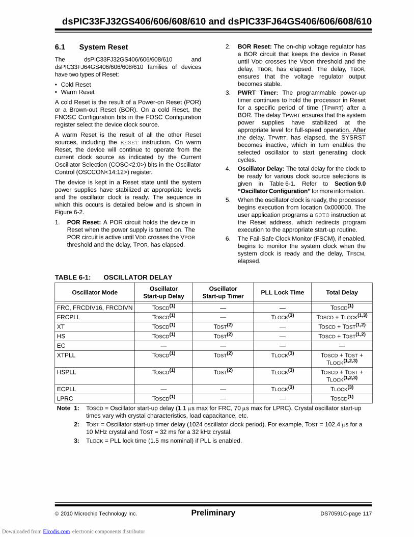
2010 Microchip Technology Inc. Preliminary DS70591C-page 117
dsPIC33FJ32GS406/606/608/610 and dsPIC33FJ64GS406/606/608/610
6.1 System Reset
The dsPIC33FJ32GS406/606/608/610 anddsPIC33FJ64GS406/606/608/610 families of deviceshave two types of Reset:
• Cold Reset• Warm Reset
A cold Reset is the result of a Power-on Reset (POR)or a Brown-out Reset (BOR). On a cold Reset, theFNOSC Configuration bits in the FOSC Configurationregister select the device clock source.
A warm Reset is the result of all the other Resetsources, including the RESET instruction. On warmReset, the device will continue to operate from thecurrent clock source as indicated by the CurrentOscillator Selection (COSC<2:0>) bits in the OscillatorControl (OSCCON<14:12>) register.
The device is kept in a Reset state until the systempower supplies have stabilized at appropriate levelsand the oscillator clock is ready. The sequence inwhich this occurs is detailed below and is shown inFigure 6-2.
1. POR Reset: A POR circuit holds the device inReset when the power supply is turned on. ThePOR circuit is active until VDD crosses the VPOR
threshold and the delay, TPOR, has elapsed.
2. BOR Reset: The on-chip voltage regulator hasa BOR circuit that keeps the device in Resetuntil VDD crosses the VBOR threshold and thedelay, TBOR, has elapsed. The delay, TBOR,ensures that the voltage regulator outputbecomes stable.
3. PWRT Timer: The programmable power-uptimer continues to hold the processor in Resetfor a specific period of time (TPWRT) after aBOR. The delay TPWRT ensures that the systempower supplies have stabilized at theappropriate level for full-speed operation. Afterthe delay, TPWRT, has elapsed, the SYSRSTbecomes inactive, which in turn enables theselected oscillator to start generating clockcycles.
4. Oscillator Delay: The total delay for the clock tobe ready for various clock source selections isgiven in Table 6-1. Refer to Section 9.0“Oscillator Configuration” for more information.
5. When the oscillator clock is ready, the processorbegins execution from location 0x000000. Theuser application programs a GOTO instruction atthe Reset address, which redirects programexecution to the appropriate start-up routine.
6. The Fail-Safe Clock Monitor (FSCM), if enabled,begins to monitor the system clock when thesystem clock is ready and the delay, TFSCM,elapsed.
TABLE 6-1: OSCILLATOR DELAY
Oscillator ModeOscillator
Start-up DelayOscillator
Start-up TimerPLL Lock Time Total Delay
FRC, FRCDIV16, FRCDIVN TOSCD(1) — — TOSCD(1)
FRCPLL TOSCD(1) — TLOCK(3) TOSCD + TLOCK(1,3)
XT TOSCD(1) TOST(2) — TOSCD + TOST(1,2)
HS TOSCD(1) TOST(2) — TOSCD + TOST(1,2)
EC — — — —
XTPLL TOSCD(1) TOST(2) TLOCK(3) TOSCD + TOST + TLOCK(1,2,3)
HSPLL TOSCD(1) TOST(2) TLOCK(3) TOSCD + TOST + TLOCK(1,2,3)
ECPLL — — TLOCK(3) TLOCK(3)
LPRC TOSCD(1) — — TOSCD(1)
Note 1: TOSCD = Oscillator start-up delay (1.1 s max for FRC, 70 s max for LPRC). Crystal oscillator start-up times vary with crystal characteristics, load capacitance, etc.
2: TOST = Oscillator start-up timer delay (1024 oscillator clock period). For example, TOST = 102.4 s for a 10 MHz crystal and TOST = 32 ms for a 32 kHz crystal.
3: TLOCK = PLL lock time (1.5 ms nominal) if PLL is enabled.
Downloaded from Elcodis.com electronic components distributor
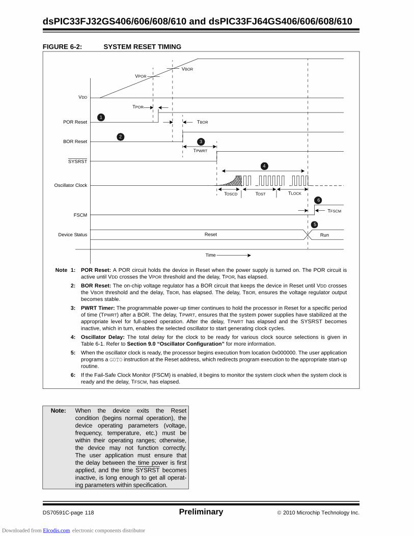
dsPIC33FJ32GS406/606/608/610 and dsPIC33FJ64GS406/606/608/610
DS70591C-page 118 Preliminary 2010 Microchip Technology Inc.
FIGURE 6-2: SYSTEM RESET TIMING
Reset RunDevice Status
VDD
VPOR
VBOR
POR Reset
BOR Reset
SYSRST
TPWRT
TPOR
TBOR
Oscillator Clock
TOSCD TOST TLOCK
Time
FSCMTFSCM
1
23
4
5
6
Note 1: POR Reset: A POR circuit holds the device in Reset when the power supply is turned on. The POR circuit isactive until VDD crosses the VPOR threshold and the delay, TPOR, has elapsed.
2: BOR Reset: The on-chip voltage regulator has a BOR circuit that keeps the device in Reset until VDD crossesthe VBOR threshold and the delay, TBOR, has elapsed. The delay, TBOR, ensures the voltage regulator outputbecomes stable.
3: PWRT Timer: The programmable power-up timer continues to hold the processor in Reset for a specific periodof time (TPWRT) after a BOR. The delay, TPWRT, ensures that the system power supplies have stabilized at theappropriate level for full-speed operation. After the delay, TPWRT has elapsed and the SYSRST becomesinactive, which in turn, enables the selected oscillator to start generating clock cycles.
4: Oscillator Delay: The total delay for the clock to be ready for various clock source selections is given inTable 6-1. Refer to Section 9.0 “Oscillator Configuration” for more information.
5: When the oscillator clock is ready, the processor begins execution from location 0x000000. The user applicationprograms a GOTO instruction at the Reset address, which redirects program execution to the appropriate start-uproutine.
6: If the Fail-Safe Clock Monitor (FSCM) is enabled, it begins to monitor the system clock when the system clock isready and the delay, TFSCM, has elapsed.
Note: When the device exits the Resetcondition (begins normal operation), thedevice operating parameters (voltage,frequency, temperature, etc.) must bewithin their operating ranges; otherwise,the device may not function correctly.The user application must ensure thatthe delay between the time power is firstapplied, and the time SYSRST becomesinactive, is long enough to get all operat-ing parameters within specification.
Downloaded from Elcodis.com electronic components distributor

2010 Microchip Technology Inc. Preliminary DS70591C-page 119
dsPIC33FJ32GS406/606/608/610 and dsPIC33FJ64GS406/606/608/610
6.2 Power-on Reset (POR)
A Power-on Reset (POR) circuit ensures the device isreset from power-on. The POR circuit is active untilVDD crosses the VPOR threshold and the delay, TPOR,has elapsed. The delay, TPOR, ensures the internaldevice bias circuits become stable.
The device supply voltage characteristics must meetthe specified starting voltage and rise raterequirements to generate the POR. Refer toSection 27.0 “Electrical Characteristics” for details.
The POR Status (POR) bit in the Reset Control(RCON<0>) register is set to indicate the Power-onReset.
6.3 Brown-out Reset (BOR) and Power-up Timer (PWRT)
The on-chip regulator has a Brown-out Reset (BOR)circuit that resets the device when the VDD is too low(VDD < VBOR) for proper device operation. The BORcircuit keeps the device in Reset until VDD crosses the
VBOR threshold and the delay, TBOR, has elapsed. Thedelay, TBOR, ensures the voltage regulator outputbecomes stable.
The BOR Status (BOR) bit in the Reset Control(RCON<1>) register is set to indicate the Brown-outReset.
The device will not run at full speed after a BOR as theVDD should rise to acceptable levels for full-speedoperation. The PWRT provides power-up time delay(TPWRT) to ensure that the system power supplies havestabilized at the appropriate levels for full-speedoperation before the SYSRST is released.
The power-up timer delay (TPWRT) is programmed bythe Power-on Reset Timer Value Select(FPWRT<2:0>) bits in the POR Configuration(FPOR<2:0>) register, which provides eight settings(from 0 ms to 128 ms). Refer to Section 24.0 “SpecialFeatures” for further details.
Figure 6-3 shows the typical brown-out scenarios. Thereset delay (TBOR + TPWRT) is initiated each time VDD
rises above the VBOR trip point
FIGURE 6-3: BROWN-OUT SITUATIONS
VDD
SYSRST
VBOR
VDD
SYSRST
VBOR
VDD
SYSRST
VBOR
TBOR + TPWRT
VDD dips before PWRT expires
TBOR + TPWRT
TBOR + TPWRT
Downloaded from Elcodis.com electronic components distributor

dsPIC33FJ32GS406/606/608/610 and dsPIC33FJ64GS406/606/608/610
DS70591C-page 120 Preliminary 2010 Microchip Technology Inc.
6.4 External Reset (EXTR)
The external Reset is generated by driving the MCLRpin low. The MCLR pin is a Schmitt Trigger input withan additional glitch filter. Reset pulses that are longerthan the minimum pulse width will generate a Reset.Refer to Section 27.0 “Electrical Characteristics” forminimum pulse width specifications. The externalReset (MCLR) pin (EXTR) bit in the Reset Control(RCON) register is set to indicate the MCLR Reset.
6.4.0.1 EXTERNAL SUPERVISORY CIRCUIT
Many systems have external supervisory circuits thatgenerate Reset signals to reset multiple devices in thesystem. This external Reset signal can be directlyconnected to the MCLR pin to reset the device whenthe rest of system is reset.
6.4.0.2 INTERNAL SUPERVISORY CIRCUIT
When using the internal power supervisory circuit toreset the device, the external Reset pin (MCLR) shouldbe tied directly or resistively to VDD. In this case, theMCLR pin will not be used to generate a Reset. Theexternal Reset pin (MCLR) does not have an internalpull-up and must not be left unconnected.
6.5 Software RESET Instruction (SWR)
Whenever the RESET instruction is executed, thedevice will assert SYSRST, placing the device in aspecial Reset state. This Reset state will notre-initialize the clock. The clock source in effect prior tothe RESET instruction will remain. SYSRST is releasedat the next instruction cycle and the Reset vector fetchwill commence.
The Software Reset (SWR) flag (instruction) in theReset Control (RCON<6>) register is set to indicatethe software Reset.
6.6 Watchdog Time-out Reset (WDTO)
Whenever a Watchdog time-out occurs, the device willasynchronously assert SYSRST. The clock source willremain unchanged. A WDT time-out during Sleep orIdle mode will wake-up the processor, but will not resetthe processor.
The Watchdog Timer Time-out (WDTO) flag in theReset Control (RCON<4>) register is set to indicatethe Watchdog Reset. Refer to Section 24.4“Watchdog Timer (WDT)” for more information onWatchdog Reset.
6.7 Trap Conflict Reset
If a lower priority hard trap occurs while a higherpriority trap is being processed, a hard Trap ConflictReset occurs. The hard traps include exceptions of pri-
ority level 13 through level 15, inclusive. The addresserror (level 13) and oscillator error (level 14) traps fallinto this category.
The Trap Reset (TRAPR) flag in the Reset Control(RCON<15>) register is set to indicate the Trap ConflictReset. Refer to Section 7.0 “Interrupt Controller” formore information on Trap Conflict Resets.
6.8 Illegal Condition Device Reset
An illegal condition device Reset occurs due to thefollowing sources:
• Illegal Opcode Reset• Uninitialized W Register Reset• Security Reset
The Illegal Opcode or Uninitialized W Access Reset(IOPUWR) flag in the Reset Control (RCON<14>)register is set to indicate the illegal condition deviceReset.
6.8.1 ILLEGAL OPCODE RESET
A device Reset is generated if the device attempts toexecute an illegal opcode value that is fetched fromprogram memory.
The Illegal Opcode Reset function can prevent thedevice from executing program memory sections thatare used to store constant data. To take advantage ofthe Illegal Opcode Reset, use only the lower 16 bits ofeach program memory section to store the data values.The upper 8 bits should be programmed with 3Fh,which is an illegal opcode value.
6.8.2 UNINITIALIZED W REGISTER RESET
Any attempt to use the uninitialized W register as anAddress Pointer will Reset the device. The W registerarray (with the exception of W15) is cleared during allResets and is considered uninitialized until written to.
6.8.3 SECURITY RESET
If a Program Flow Change (PFC) or Vector FlowChange (VFC) targets a restricted location in aprotected segment (boot and secure segment), thatoperation will cause a Security Reset.
The PFC occurs when the program counter is reloadedas a result of a call, jump, computed jump, return,return from subroutine or other form of branchinstruction.
The VFC occurs when the program counter is reloadedwith an interrupt or trap vector.
Refer to Section 24.8 “Code Protection andCodeGuard™ Security” for more information onSecurity Reset.
Downloaded from Elcodis.com electronic components distributor
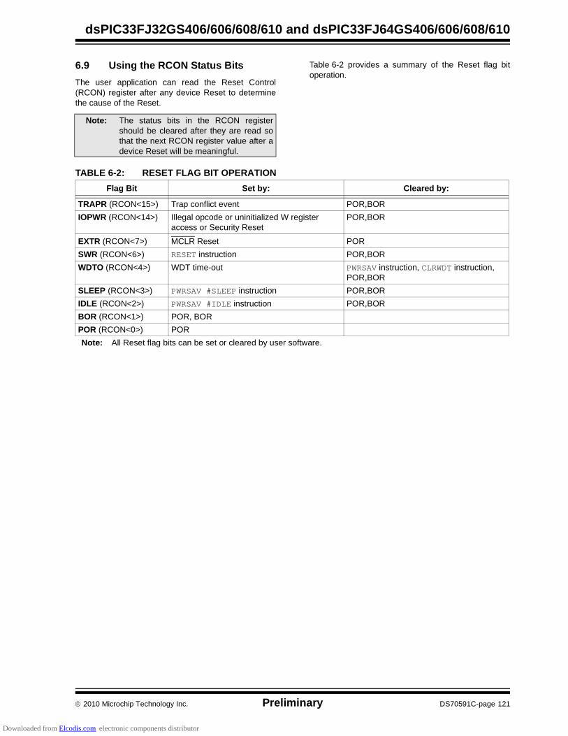
2010 Microchip Technology Inc. Preliminary DS70591C-page 121
dsPIC33FJ32GS406/606/608/610 and dsPIC33FJ64GS406/606/608/610
6.9 Using the RCON Status Bits
The user application can read the Reset Control(RCON) register after any device Reset to determinethe cause of the Reset.
Table 6-2 provides a summary of the Reset flag bitoperation.
TABLE 6-2: RESET FLAG BIT OPERATION
Note: The status bits in the RCON registershould be cleared after they are read sothat the next RCON register value after adevice Reset will be meaningful.
Flag Bit Set by: Cleared by:
TRAPR (RCON<15>) Trap conflict event POR,BOR
IOPWR (RCON<14>) Illegal opcode or uninitialized W register access or Security Reset
POR,BOR
EXTR (RCON<7>) MCLR Reset POR
SWR (RCON<6>) RESET instruction POR,BOR
WDTO (RCON<4>) WDT time-out PWRSAV instruction, CLRWDT instruction, POR,BOR
SLEEP (RCON<3>) PWRSAV #SLEEP instruction POR,BOR
IDLE (RCON<2>) PWRSAV #IDLE instruction POR,BOR
BOR (RCON<1>) POR, BOR
POR (RCON<0>) POR
Note: All Reset flag bits can be set or cleared by user software.
Downloaded from Elcodis.com electronic components distributor

dsPIC33FJ32GS406/606/608/610 and dsPIC33FJ64GS406/606/608/610
DS70591C-page 122 Preliminary 2010 Microchip Technology Inc.
NOTES:
Downloaded from Elcodis.com electronic components distributor

2010 Microchip Technology Inc. Preliminary DS70591C-page 123
dsPIC33FJ32GS406/606/608/610 and dsPIC33FJ64GS406/606/608/610
7.0 INTERRUPT CONTROLLER
The dsPIC33FJ32GS406/606/608/610 anddsPIC33FJ64GS406/606/608/610 interrupt controllerreduces the numerous peripheral interrupt requestsignals to a single interrupt request signal to thedsPIC33FJ32GS406/606/608/610 anddsPIC33FJ64GS406/606/608/610 CPU. It has thefollowing features:
• Up to eight processor exceptions and software traps
• Seven user-selectable priority levels
• Interrupt Vector Table (IVT) with up to 118 vectors
• A unique vector for each interrupt or exception source
• Fixed priority within a specified user priority level
• Alternate Interrupt Vector Table (AIVT) for debug support
• Fixed interrupt entry and return latencies
7.1 Interrupt Vector Table
The Interrupt Vector Table (IVT) is shown in Figure 7-1.The IVT resides in program memory, starting at location000004h. The IVT contains 126 vectors, consisting ofeight nonmaskable trap vectors, plus up to 118 sourcesof interrupt. In general, each interrupt source has its ownvector. Each interrupt vector contains a 24-bit-wideaddress. The value programmed into each interruptvector location is the starting address of the associatedInterrupt Service Routine (ISR).
Interrupt vectors are prioritized in terms of their naturalpriority. This priority is linked to their position in thevector table. Lower addresses generally have a highernatural priority. For example, the interrupt associatedwith vector 0 will take priority over interrupts at anyother vector address.
The dsPIC33FJ32GS406/606/608/610 anddsPIC33FJ64GS406/606/608/610 devices implement upto 71 unique interrupts and five non-maskable traps.These are summarized in Table 7-1.
7.1.1 ALTERNATE INTERRUPT VECTOR TABLE
The Alternate Interrupt Vector Table (AIVT) is locatedafter the IVT, as shown in Figure 7-1. Access to theAIVT is provided by the ALTIVT control bit(INTCON2<15>). If the ALTIVT bit is set, all interruptand exception processes use the alternate vectorsinstead of the default vectors. The alternate vectors areorganized in the same manner as the default vectors.
The AIVT supports debugging by providing a means toswitch between an application and a supportenvironment without requiring the interrupt vectors tobe reprogrammed. This feature also enables switchingbetween applications for evaluation of differentsoftware algorithms at run time. If the AIVT is notneeded, the AIVT should be programmed with thesame addresses used in the IVT.
7.2 Reset Sequence
A device Reset is not a true exception because theinterrupt controller is not involved in the Reset process.The dsPIC33FJ32GS406/606/608/610 anddsPIC33FJ64GS406/606/608/610 device clears itsregisters in response to a Reset, which forces the PC tozero. The digital signal controller then begins programexecution at location 0x000000. A GOTO instruction at theReset address can redirect program execution to theappropriate start-up routine.
Note 1: This data sheet summarizes the featuresof the dsPIC33FJ32GS406/606/608/610and dsPIC33FJ64GS406/606/608/610families of devices. It is not intended to bea comprehensive reference source. Tocomplement the information in this datasheet, refer to Section 47. “Interrupts(Part V)” (DS70597) in the “dsPIC33F/PIC24H Family Reference Manual”,which is available from the Microchip website (www.microchip.com).
2: Some registers and associated bitsdescribed in this section may not be avail-able on all devices. Refer to Section 4.0“Memory Organization” in this datasheet for device-specific register and bitinformation.
Note: Any unimplemented or unused vectorlocations in the IVT and AIVT should beprogrammed with the address of a defaultinterrupt handler routine that contains aRESET instruction.
Downloaded from Elcodis.com electronic components distributor
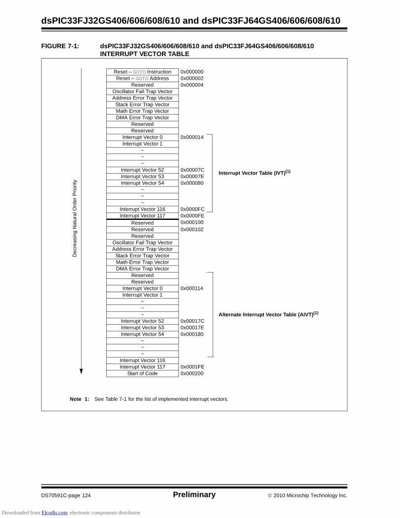
dsPIC33FJ32GS406/606/608/610 and dsPIC33FJ64GS406/606/608/610
DS70591C-page 124 Preliminary 2010 Microchip Technology Inc.
FIGURE 7-1: dsPIC33FJ32GS406/606/608/610 and dsPIC33FJ64GS406/606/608/610 INTERRUPT VECTOR TABLE
Reset – GOTO Instruction 0x000000Reset – GOTO Address 0x000002
Reserved 0x000004Oscillator Fail Trap VectorAddress Error Trap Vector
Stack Error Trap VectorMath Error Trap VectorDMA Error Trap Vector
ReservedReserved
Interrupt Vector 0 0x000014Interrupt Vector 1
~~~
Interrupt Vector 52 0x00007CInterrupt Vector 53 0x00007EInterrupt Vector 54 0x000080
~~~
Interrupt Vector 116 0x0000FCInterrupt Vector 117 0x0000FE
Reserved 0x000100Reserved 0x000102Reserved
Oscillator Fail Trap VectorAddress Error Trap Vector
Stack Error Trap VectorMath Error Trap VectorDMA Error Trap Vector
ReservedReserved
Interrupt Vector 0 0x000114Interrupt Vector 1
~~~
Interrupt Vector 52 0x00017CInterrupt Vector 53 0x00017EInterrupt Vector 54 0x000180
~~~
Interrupt Vector 116Interrupt Vector 117 0x0001FE
Start of Code 0x000200
De
cre
asi
ng
Na
tura
l Ord
er
Pri
ori
ty
Interrupt Vector Table (IVT)(1)
Alternate Interrupt Vector Table (AIVT)(1)
Note 1: See Table 7-1 for the list of implemented interrupt vectors.
Downloaded from Elcodis.com electronic components distributor
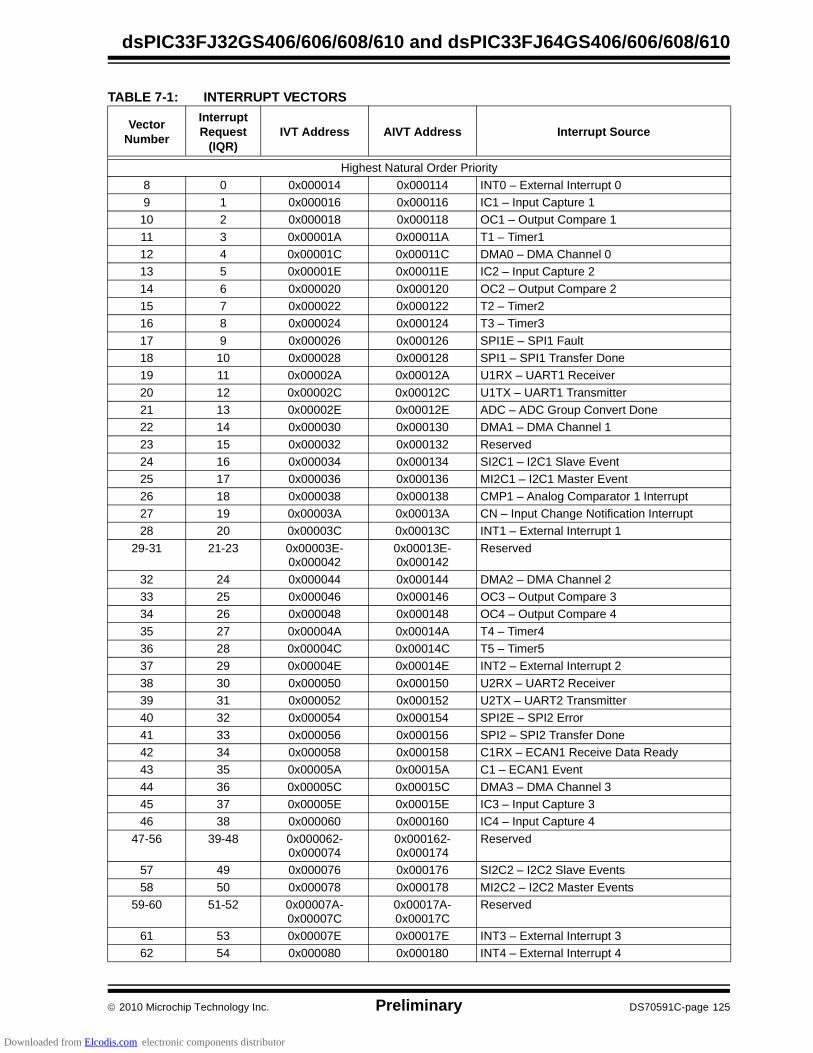
2010 Microchip Technology Inc. Preliminary DS70591C-page 125
dsPIC33FJ32GS406/606/608/610 and dsPIC33FJ64GS406/606/608/610
TABLE 7-1: INTERRUPT VECTORS
Vector Number
Interrupt Request
(IQR)IVT Address AIVT Address Interrupt Source
Highest Natural Order Priority
8 0 0x000014 0x000114 INT0 – External Interrupt 0
9 1 0x000016 0x000116 IC1 – Input Capture 1
10 2 0x000018 0x000118 OC1 – Output Compare 1
11 3 0x00001A 0x00011A T1 – Timer1
12 4 0x00001C 0x00011C DMA0 – DMA Channel 0
13 5 0x00001E 0x00011E IC2 – Input Capture 2
14 6 0x000020 0x000120 OC2 – Output Compare 2
15 7 0x000022 0x000122 T2 – Timer2
16 8 0x000024 0x000124 T3 – Timer3
17 9 0x000026 0x000126 SPI1E – SPI1 Fault
18 10 0x000028 0x000128 SPI1 – SPI1 Transfer Done
19 11 0x00002A 0x00012A U1RX – UART1 Receiver
20 12 0x00002C 0x00012C U1TX – UART1 Transmitter
21 13 0x00002E 0x00012E ADC – ADC Group Convert Done
22 14 0x000030 0x000130 DMA1 – DMA Channel 1
23 15 0x000032 0x000132 Reserved
24 16 0x000034 0x000134 SI2C1 – I2C1 Slave Event
25 17 0x000036 0x000136 MI2C1 – I2C1 Master Event
26 18 0x000038 0x000138 CMP1 – Analog Comparator 1 Interrupt
27 19 0x00003A 0x00013A CN – Input Change Notification Interrupt
28 20 0x00003C 0x00013C INT1 – External Interrupt 1
29-31 21-23 0x00003E-0x000042
0x00013E-0x000142
Reserved
32 24 0x000044 0x000144 DMA2 – DMA Channel 2
33 25 0x000046 0x000146 OC3 – Output Compare 3
34 26 0x000048 0x000148 OC4 – Output Compare 4
35 27 0x00004A 0x00014A T4 – Timer4
36 28 0x00004C 0x00014C T5 – Timer5
37 29 0x00004E 0x00014E INT2 – External Interrupt 2
38 30 0x000050 0x000150 U2RX – UART2 Receiver
39 31 0x000052 0x000152 U2TX – UART2 Transmitter
40 32 0x000054 0x000154 SPI2E – SPI2 Error
41 33 0x000056 0x000156 SPI2 – SPI2 Transfer Done
42 34 0x000058 0x000158 C1RX – ECAN1 Receive Data Ready
43 35 0x00005A 0x00015A C1 – ECAN1 Event
44 36 0x00005C 0x00015C DMA3 – DMA Channel 3
45 37 0x00005E 0x00015E IC3 – Input Capture 3
46 38 0x000060 0x000160 IC4 – Input Capture 4
47-56 39-48 0x000062-0x000074
0x000162-0x000174
Reserved
57 49 0x000076 0x000176 SI2C2 – I2C2 Slave Events
58 50 0x000078 0x000178 MI2C2 – I2C2 Master Events
59-60 51-52 0x00007A-0x00007C
0x00017A-0x00017C
Reserved
61 53 0x00007E 0x00017E INT3 – External Interrupt 3
62 54 0x000080 0x000180 INT4 – External Interrupt 4
Downloaded from Elcodis.com electronic components distributor

dsPIC33FJ32GS406/606/608/610 and dsPIC33FJ64GS406/606/608/610
DS70591C-page 126 Preliminary 2010 Microchip Technology Inc.
63-64 55-56 0x000082-0x000084
0x000182-0x000184
Reserved
65 57 0x000086 0x000186 PWM PSEM Special Event Match
66 58 0x000088 0x000188 QEI1 – Position Counter Compare
67-72 59-64 0x00008A-0x000094
0x00018A-0x000194
Reserved
73 65 0x000096 0x000196 U1E – UART1 Error Interrupt
74 66 0x000098 0x000198 U2E – UART2 Error Interrupt
75-77 67-69 0x00009A-0x00009E
0x00019A-0x00019E
Reserved
78 70 0x0000A0 0x0001A0 C1TX – ECAN1 Transmit Data Request
79 71 0x0000A2 0x0001A2 Reserved
80 72 0x0000A4 0x0001A4 Reserved
81 73 0x0000A6 0x0001A6 PWM Secondary Special Event Match
82 74 0x0000A8 0x0001A8 Reserved
83 75 0x0000AA 0x0001AA QEI2 – Position Counter Compare
84-88 76-80 0x0000AC-0x0000B4
0x0001AC-0x0001B4
Reserved
89 81 0x0000B6 0x0001B6 ADC Pair 8 Conversion Done
90 82 0x0000B8 0x0001B8 ADC Pair 9 Conversion Done
91 83 0x0000BA 0x0001BA ADC Pair 10 Conversion Done
92 84 0x0000BC 0x0001BC ADC Pair 11 Conversion Done
93 85 0x0000BE 0x0001BE ADC Pair 12 Conversion Done
94-101 86-93 0x0000C0-0x0000CE
0x0001C0-0x0001CE
Reserved
102 94 0x0000D0 0x0001D0 PWM1 – PWM1 Interrupt
103 95 0x0000D2 0x0001D2 PWM2 – PWM2 Interrupt
104 96 0x0000D4 0x0001D4 PWM3 – PWM3 Interrupt
105 97 0x0000D6 0x0001D6 PWM4 – PWM4 Interrupt
106 98 0x0000D8 0x0001D8 PWM5 – PWM5 Interrupt
107 99 0x0000DA 0x0001DA PWM6 – PWM6 Interrupt
108 100 0x0000DC 0x0001DC PWM7– PWM7 Interrupt
109 101 0x0000DE 0x0001DE PWM8 – PWM8 Interrupt
110 102 0x0000E0 0x0001E0 PWM9 – PWM9 Interrupt
111 103 0x0000E2 0x00001E2 CMP2 – Analog Comparator 2
112 104 0x0000E4 0x0001E4 CMP3 – Analog Comparator 3
113 105 0x0000E6 0x0001E6 CMP4 – Analog Comparator 4
114-117 106-109 0x0000E8-0x0000EE
0x0001E8-0x0001EE
Reserved
118 110 0x0000F0 0x0001F0 ADC Pair 0 Convert Done
119 111 0x0000F2 0x0001F2 ADC Pair 1 Convert Done
120 112 0x0000F4 0x0001F4 ADC Pair 2 Convert Done
121 113 0x0000F6 0x0001F6 ADC Pair 3 Convert Done
122 114 0x0000F8 0x0001F8 ADC Pair 4 Convert Done
123 115 0x0000FA 0x0001FA ADC Pair 5 Convert Done
124 116 0x0000FC 0x0001FC ADC Pair 6 Convert Done
125 117 0x0000FE 0x0001FE ADC Pair 7 Convert Done
Lowest Natural Order Priority
TABLE 7-1: INTERRUPT VECTORS (CONTINUED)
Vector Number
Interrupt Request
(IQR)IVT Address AIVT Address Interrupt Source
Downloaded from Elcodis.com electronic components distributor

2010 Microchip Technology Inc. Preliminary DS70591C-page 127
dsPIC33FJ32GS406/606/608/610 and dsPIC33FJ64GS406/606/608/610
7.3 Interrupt Control and Status Registers
The dsPIC33FJ32GS406/606/608/610 anddsPIC33FJ64GS406/606/608/610 devices implement 27registers for the interrupt controller:
• INTCON1 • INTCON2 • IFSx• IECx• IPCx • INTTREG
7.3.1 INTCON1 AND INTCON2
Global interrupt control functions are controlled fromINTCON1 and INTCON2. INTCON1 contains theInterrupt Nesting Disable (NSTDIS) bit as well as thecontrol and status flags for the processor trap sources.The INTCON2 register controls the external interruptrequest signal behavior and the use of the AlternateInterrupt Vector Table.
7.3.2 IFSx
The IFSx registers maintain all of the interrupt requestflags. Each source of interrupt has a status bit, which isset by the respective peripherals or external signal andis cleared via software.
7.3.3 IECx
The IECx registers maintain all of the interrupt enablebits. These control bits are used to individually enableinterrupts from the peripherals or external signals.
7.3.4 IPCx
The IPCx registers are used to set the Interrupt PriorityLevel for each source of interrupt. Each user interruptsource can be assigned to one of eight priority levels.
7.3.5 INTTREG
The INTTREG register contains the associatedinterrupt vector number and the new CPU Interruptpriority Level, which are latched into the Vector Number(VECNUM<6:0>) and Interrupt Level (ILR<3:0>) bitfields in the INTTREG register. The new InterruptPriority Level is the priority of the pending interrupt.
The interrupt sources are assigned to the IFSx, IECxand IPCx registers in the same sequence that they arelisted in Table 7-1. For example, the INT0 (ExternalInterrupt 0) is shown as having vector number 8 and anatural order priority of 0. Thus, the INT0IF bit is foundin IFS0<0>, the INT0IE bit is found in IEC0<0> and theINT0IP bits are found in the first position of IPC0(IPC0<2:0>).
7.3.6 STATUS/CONTROL REGISTERS
Although they are not specifically part of the interruptcontrol hardware, two of the CPU Control registerscontain bits that control interrupt functionality.
• The CPU STATUS register, SR, contains theIPL<2:0> bits (SR<7:5>). These bits indicate thecurrent CPU interrupt Priority Level. The user canchange the current CPU priority level by writing tothe IPL bits.
• The CORCON register contains the IPL3 bit,which together with IPL<2:0>, indicates thecurrent CPU priority level. IPL3 is a read-only bitso that trap events cannot be masked by the usersoftware.
All Interrupt registers are described in Register 7-1through Register 7-46 in the following pages.
Downloaded from Elcodis.com electronic components distributor

dsPIC33FJ32GS406/606/608/610 and dsPIC33FJ64GS406/606/608/610
DS70591C-page 128 Preliminary 2010 Microchip Technology Inc.
REGISTER 7-1: SR: CPU STATUS REGISTER(1)
REGISTER 7-2: CORCON: CORE CONTROL REGISTER(1)
R-0 R-0 R/C-0 R/C-0 R-0 R/C-0 R -0 R/W-0
OA OB SA SB OAB SAB DA DC
bit 15 bit 8
R/W-0(3) R/W-0(3) R/W-0(3) R-0 R/W-0 R/W-0 R/W-0 R/W-0
IPL2(2) IPL1(2) IPL0(2) RA N OV Z C
bit 7 bit 0
Legend:
C = Clearable bit R = Readable bit U = Unimplemented bit, read as ‘0’
S = Settable bit W = Writable bit -n = Value at POR
‘1’ = Bit is set ‘0’ = Bit is cleared x = Bit is unknown
bit 7-5 IPL<2:0>: CPU Interrupt Priority Level Status bits(2)
111 = CPU Interrupt Priority Level is 7 (15), user interrupts disabled110 = CPU Interrupt Priority Level is 6 (14)101 = CPU Interrupt Priority Level is 5 (13)100 = CPU Interrupt Priority Level is 4 (12)011 = CPU Interrupt Priority Level is 3 (11)010 = CPU Interrupt Priority Level is 2 (10)001 = CPU Interrupt Priority Level is 1 (9)000 = CPU Interrupt Priority Level is 0 (8)
Note 1: For complete register details, see Register 3-1.
2: The IPL<2:0> bits are concatenated with the IPL<3> bit (CORCON<3>) to form the CPU Interrupt PriorityLevel. The value in parentheses indicates the IPL if IPL<3> = 1. User interrupts are disabled whenIPL<3> = 1.
3: The IPL<2:0> Status bits are read-only when NSTDIS (INTCON1<15>) = 1.
U-0 U-0 U-0 U-0 R/W-0 R-0 R-0 R-0
— — — US EDT DL<2:0>
bit 15 bit 8
R/W-0 R/W-0 R/W-1 R/W-0 R/C-0 R/W-0 R/W-0 R/W-0
SATA SATB SATDW ACCSAT IPL3(2) PSV RND IF
bit 7 bit 0
Legend: C = Clearable bit
R = Readable bit W = Writable bit -n = Value at POR ‘1’ = Bit is set
0’ = Bit is cleared ‘x = Bit is unknown U = Unimplemented bit, read as ‘0’
bit 3 IPL3: CPU Interrupt Priority Level Status bit 3(2)
1 = CPU Interrupt Priority Level is greater than 70 = CPU Interrupt Priority Level is 7 or less
Note 1: For complete register details, see Register 3-2.
2: The IPL3 bit is concatenated with the IPL<2:0> bits (SR<7:5>) to form the CPU Interrupt Priority Level.
Downloaded from Elcodis.com electronic components distributor

2010 Microchip Technology Inc. Preliminary DS70591C-page 129
dsPIC33FJ32GS406/606/608/610 and dsPIC33FJ64GS406/606/608/610
REGISTER 7-3: INTCON1: INTERRUPT CONTROL REGISTER 1
R/W-0 R/W-0 R/W-0 R/W-0 R/W-0 R/W-0 R/W-0 R/W-0
NSTDIS OVAERR OVBERR COVAERR COVBERR OVATE OVBTE COVTE
bit 15 bit 8
R/W-0 R/W-0 R/W-0 R/W-0 R/W-0 R/W-0 R/W-0 U-0
SFTACERR DIV0ERR DMACERR MATHERR ADDRERR STKERR OSCFAIL —
bit 7 bit 0
Legend:
R = Readable bit W = Writable bit U = Unimplemented bit, read as ‘0’
-n = Value at POR ‘1’ = Bit is set ‘0’ = Bit is cleared x = Bit is unknown
bit 15 NSTDIS: Interrupt Nesting Disable bit
1 = Interrupt nesting is disabled0 = Interrupt nesting is enabled
bit 14 OVAERR: Accumulator A Overflow Trap Flag bit
1 = Trap was caused by overflow of Accumulator A0 = Trap was not caused by overflow of Accumulator A
bit 13 OVBERR: Accumulator B Overflow Trap Flag bit
1 = Trap was caused by overflow of Accumulator B0 = Trap was not caused by overflow of Accumulator B
bit 12 COVAERR: Accumulator A Catastrophic Overflow Trap Flag bit
1 = Trap was caused by catastrophic overflow of Accumulator A 0 = Trap was not caused by catastrophic overflow of Accumulator A
bit 11 COVBERR: Accumulator B Catastrophic Overflow Trap Flag bit
1 = Trap was caused by catastrophic overflow of Accumulator B 0 = Trap was not caused by catastrophic overflow of Accumulator B
bit 10 OVATE: Accumulator A Overflow Trap Enable bit
1 = Trap overflow of Accumulator A0 = Trap disabled
bit 9 OVBTE: Accumulator B Overflow Trap Enable bit
1 = Trap overflow of Accumulator B0 = Trap disabled
bit 8 COVTE: Catastrophic Overflow Trap Enable bit
1 = Trap on catastrophic overflow of Accumulator A or B enabled0 = Trap disabled
bit 7 SFTACERR: Shift Accumulator Error Status bit
1 = Math error trap was caused by an invalid accumulator shift0 = Math error trap was not caused by an invalid accumulator shift
bit 6 DIV0ERR: Arithmetic Error Status bit
1 = Math error trap was caused by a divide by zero0 = Math error trap was not caused by a divide by zero
bit 5 DMACERR: DMA Controller Error Status bit
1 = DMA controller error trap has occurred0 = DMA controller error trap has not occurred
bit 4 MATHERR: Arithmetic Error Status bit
1 = Math error trap has occurred0 = Math error trap has not occurred
Downloaded from Elcodis.com electronic components distributor

dsPIC33FJ32GS406/606/608/610 and dsPIC33FJ64GS406/606/608/610
DS70591C-page 130 Preliminary 2010 Microchip Technology Inc.
bit 3 ADDRERR: Address Error Trap Status bit
1 = Address error trap has occurred0 = Address error trap has not occurred
bit 2 STKERR: Stack Error Trap Status bit
1 = Stack error trap has occurred0 = Stack error trap has not occurred
bit 1 OSCFAIL: Oscillator Failure Trap Status bit
1 = Oscillator failure trap has occurred0 = Oscillator failure trap has not occurred
bit 0 Unimplemented: Read as ‘0’
REGISTER 7-3: INTCON1: INTERRUPT CONTROL REGISTER 1 (CONTINUED)
Downloaded from Elcodis.com electronic components distributor
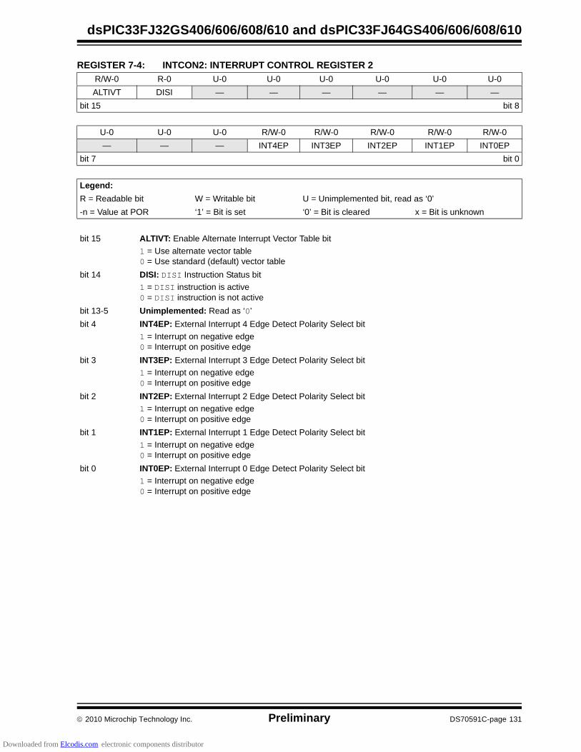
2010 Microchip Technology Inc. Preliminary DS70591C-page 131
dsPIC33FJ32GS406/606/608/610 and dsPIC33FJ64GS406/606/608/610
REGISTER 7-4: INTCON2: INTERRUPT CONTROL REGISTER 2
R/W-0 R-0 U-0 U-0 U-0 U-0 U-0 U-0
ALTIVT DISI — — — — — —
bit 15 bit 8
U-0 U-0 U-0 R/W-0 R/W-0 R/W-0 R/W-0 R/W-0
— — — INT4EP INT3EP INT2EP INT1EP INT0EP
bit 7 bit 0
Legend:
R = Readable bit W = Writable bit U = Unimplemented bit, read as ‘0’
-n = Value at POR ‘1’ = Bit is set ‘0’ = Bit is cleared x = Bit is unknown
bit 15 ALTIVT: Enable Alternate Interrupt Vector Table bit
1 = Use alternate vector table0 = Use standard (default) vector table
bit 14 DISI: DISI Instruction Status bit
1 = DISI instruction is active0 = DISI instruction is not active
bit 13-5 Unimplemented: Read as ‘0’
bit 4 INT4EP: External Interrupt 4 Edge Detect Polarity Select bit
1 = Interrupt on negative edge 0 = Interrupt on positive edge
bit 3 INT3EP: External Interrupt 3 Edge Detect Polarity Select bit
1 = Interrupt on negative edge 0 = Interrupt on positive edge
bit 2 INT2EP: External Interrupt 2 Edge Detect Polarity Select bit
1 = Interrupt on negative edge 0 = Interrupt on positive edge
bit 1 INT1EP: External Interrupt 1 Edge Detect Polarity Select bit
1 = Interrupt on negative edge 0 = Interrupt on positive edge
bit 0 INT0EP: External Interrupt 0 Edge Detect Polarity Select bit
1 = Interrupt on negative edge 0 = Interrupt on positive edge
Downloaded from Elcodis.com electronic components distributor

dsPIC33FJ32GS406/606/608/610 and dsPIC33FJ64GS406/606/608/610
DS70591C-page 132 Preliminary 2010 Microchip Technology Inc.
REGISTER 7-5: IFS0: INTERRUPT FLAG STATUS REGISTER 0
U-0 R/W-0 R/W-0 R/W-0 R/W-0 R/W-0 R/W-0 R/W-0
— DMA1IF ADIF U1TXIF U1RXIF SPI1IF SPI1EIF T3IF
bit 15 bit 8
R/W-0 R/W-0 R/W-0 R/W-0 R/W-0 R/W-0 R/W-0 R/W-0
T2IF OC2IF IC2IF DMA0IF T1IF OC1IF IC1IF INT0IF
bit 7 bit 0
Legend:
R = Readable bit W = Writable bit U = Unimplemented bit, read as ‘0’
-n = Value at POR ‘1’ = Bit is set ‘0’ = Bit is cleared x = Bit is unknown
bit 15 Unimplemented: Read as ‘0’
bit 14 DMA1IF: DMA Channel 1 Data Transfer Complete Interrupt Flag Status bit
1 = Interrupt request has occurred0 = Interrupt request has not occurred
bit 13 ADIF: ADC Group Conversion Complete Interrupt Flag Status bit
1 = Interrupt request has occurred0 = Interrupt request has not occurred
bit 12 U1TXIF: UART1 Transmitter Interrupt Flag Status bit
1 = Interrupt request has occurred0 = Interrupt request has not occurred
bit 11 U1RXIF: UART1 Receiver Interrupt Flag Status bit
1 = Interrupt request has occurred0 = Interrupt request has not occurred
bit 10 SPI1IF: SPI1 Event Interrupt Flag Status bit
1 = Interrupt request has occurred0 = Interrupt request has not occurred
bit 9 SPI1EIF: SPI1 Fault Interrupt Flag Status bit
1 = Interrupt request has occurred0 = Interrupt request has not occurred
bit 8 T3IF: Timer3 Interrupt Flag Status bit
1 = Interrupt request has occurred0 = Interrupt request has not occurred
bit 7 T2IF: Timer2 Interrupt Flag Status bit
1 = Interrupt request has occurred0 = Interrupt request has not occurred
bit 6 OC2IF: Output Compare Channel 2 Interrupt Flag Status bit
1 = Interrupt request has occurred0 = Interrupt request has not occurred
bit 5 IC2IF: Input Capture Channel 2 Interrupt Flag Status bit
1 = Interrupt request has occurred0 = Interrupt request has not occurred
bit 4 DMA0IF: DMA Channel 0 Data Transfer Complete Interrupt Flag Status bit
1 = Interrupt request has occurred0 = Interrupt request has not occurred
bit 3 T1IF: Timer1 Interrupt Flag Status bit
1 = Interrupt request has occurred0 = Interrupt request has not occurred
Downloaded from Elcodis.com electronic components distributor

2010 Microchip Technology Inc. Preliminary DS70591C-page 133
dsPIC33FJ32GS406/606/608/610 and dsPIC33FJ64GS406/606/608/610
bit 2 OC1IF: Output Compare Channel 1 Interrupt Flag Status bit
1 = Interrupt request has occurred0 = Interrupt request has not occurred
bit 1 IC1IF: Input Capture Channel 1 Interrupt Flag Status bit
1 = Interrupt request has occurred0 = Interrupt request has not occurred
bit 0 INT0IF: External Interrupt 0 Flag Status bit
1 = Interrupt request has occurred0 = Interrupt request has not occurred
REGISTER 7-5: IFS0: INTERRUPT FLAG STATUS REGISTER 0 (CONTINUED)
Downloaded from Elcodis.com electronic components distributor

dsPIC33FJ32GS406/606/608/610 and dsPIC33FJ64GS406/606/608/610
DS70591C-page 134 Preliminary 2010 Microchip Technology Inc.
REGISTER 7-6: IFS1: INTERRUPT FLAG STATUS REGISTER 1R/W-0 R/W-0 R/W-0 R/W-0 R/W-0 R/W-0 R/W-0 R/W-0
U2TXIF U2RXIF INT2IF T5IF T4IF OC4IF OC3IF DMA2IF
bit 15 bit 8
U-0 U-0 U-0 R/W-0 R/W-0 R/W-0 R/W-0 R/W-0
— — — INT1IF CNIF AC1IF MI2C1IF SI2C1IF
bit 7 bit 0
Legend:
R = Readable bit W = Writable bit U = Unimplemented bit, read as ‘0’
-n = Value at POR ‘1’ = Bit is set ‘0’ = Bit is cleared x = Bit is unknown
bit 12 U2TXIF: UART2 Transmitter Interrupt Flag Status bit
1 = Interrupt request has occurred0 = Interrupt request has not occurred
bit 11 U2RXIF: UART2 Receiver Interrupt Flag Status bit
1 = Interrupt request has occurred0 = Interrupt request has not occurred
bit 13 INT2IF: External Interrupt 2 Flag Status bit
1 = Interrupt request has occurred0 = Interrupt request has not occurred
bit 12 T5IF: Timer5 Interrupt Flag Status bit
1 = Interrupt request has occurred0 = Interrupt request has not occurred
bit 11 T4IF: Timer4 Interrupt Flag Status bit
1 = Interrupt request has occurred0 = Interrupt request has not occurred
bit 10 OC4IF: Output Compare Channel 4 Interrupt Flag Status bit
1 = Interrupt request has occurred0 = Interrupt request has not occurred
bit 9 OC3IF: Output Compare Channel 3 Interrupt Flag Status bit
1 = Interrupt request has occurred0 = Interrupt request has not occurred
bit 8 DMA2IF: DMA Channel 2 Data Transfer Complete Interrupt Flag Status bit
1 = Interrupt request has occurred0 = Interrupt request has not occurred
bit 7-5 Unimplemented: Read as ‘0’
bit 4 INT1IF: External Interrupt 1 Flag Status bit
1 = Interrupt request has occurred0 = Interrupt request has not occurred
bit 3 CNIF: Input Change Notification Interrupt Flag Status bit
1 = Interrupt request has occurred0 = Interrupt request has not occurred
bit 2 AC1IF: Analog Comparator 1 Interrupt Flag Status bit
1 = Interrupt request has occurred0 = Interrupt request has not occurred
bit 1 MI2C1IF: I2C1 Master Events Interrupt Flag Status bit
1 = Interrupt request has occurred0 = Interrupt request has not occurred
bit 0 SI2C1IF: I2C1 Slave Events Interrupt Flag Status bit
1 = Interrupt request has occurred0 = Interrupt request has not occurred
Downloaded from Elcodis.com electronic components distributor

2010 Microchip Technology Inc. Preliminary DS70591C-page 135
dsPIC33FJ32GS406/606/608/610 and dsPIC33FJ64GS406/606/608/610
REGISTER 7-7: IFS2: INTERRUPT FLAG STATUS REGISTER 2
U-0 U-0 U-0 U-0 U-0 U-0 U-0 U-0
— — — — — — — —
bit 15 bit 8
U-0 R/W-0 R/W-0 R/W-0 R/W-0 R/W-0 R/W-0 R/W-0
— IC4IF IC3IF DMA3IF C1IF(1) C1EIF(1) SPI2IF SPI2EIF
bit 7 bit 0
Legend:
R = Readable bit W = Writable bit U = Unimplemented bit, read as ‘0’
-n = Value at POR ‘1’ = Bit is set ‘0’ = Bit is cleared x = Bit is unknown
bit 15-7 Unimplemented: Read as ‘0’
bit 6 IC4IF: Input Capture Channel 4 Interrupt Flag Status bit
1 = Interrupt request has occurred0 = Interrupt request has not occurred
bit 5 IC3IF: Input Capture Channel 3 Interrupt Flag Status bit
1 = Interrupt request has occurred0 = Interrupt request has not occurred
bit 4 DMA3IF: DMA Channel 3 Data Transfer Complete Interrupt Flag Status bit
1 = Interrupt request has occurred0 = Interrupt request has not occurred
bit 3 C1IF: ECAN1 Event Interrupt Flag Status bit(1)
1 = Interrupt request has occurred0 = Interrupt request has not occurred
bit 2 C1EIF: ECAN1 External Event Interrupt Flag Status bit(1)
1 = Interrupt request has occurred0 = Interrupt request has not occurred
bit 1 SPI2IF: SPI2 Event Interrupt Flag Status bit
1 = Interrupt request has occurred0 = Interrupt request has not occurred
bit 0 SPI2EIF: SPI2 Error Interrupt Flag Status bit
1 = Interrupt request has occurred0 = Interrupt request has not occurred
Note 1: Interrupts disabled on devices without ECAN™ modules
Downloaded from Elcodis.com electronic components distributor

dsPIC33FJ32GS406/606/608/610 and dsPIC33FJ64GS406/606/608/610
DS70591C-page 136 Preliminary 2010 Microchip Technology Inc.
REGISTER 7-8: IFS3: INTERRUPT FLAG STATUS REGISTER 3
U-0 U-0 U-0 U-0 U-0 R/W-0 R/W-0 U-0
— — — — — QEI1IF PSEMIF —
bit 15 bit 8
U-0 R/W-0 R/W-0 U-0 U-0 R/W-0 R/W-0 U-0
— INT4IF INT3IF — — MI2C2IF SI2C2IF —
bit 7 bit 0
Legend:
R = Readable bit W = Writable bit U = Unimplemented bit, read as ‘0’
-n = Value at POR ‘1’ = Bit is set ‘0’ = Bit is cleared x = Bit is unknown
bit 15-11 Unimplemented: Read as ‘0’
bit 10 QEI1IF: QEI1 Event Interrupt Flag Status bit
1 = Interrupt request has occurred0 = Interrupt request has not occurred
bit 9 PSEMIF: PWM Special Event Match Interrupt Flag Status bit
1 = Interrupt request has occurred0 = Interrupt request has not occurred
bit 8-7 Unimplemented: Read as ‘0’
bit 6 INT4IF: External Interrupt 4 Flag Status bit
1 = Interrupt request has occurred0 = Interrupt request has not occurred
bit 5 INT3IF: External Interrupt 3 Flag Status bit
1 = Interrupt request has occurred0 = Interrupt request has not occurred
bit 4-3 Unimplemented: Read as ‘0’
bit 2 MI2C2IF: I2C2 Master Events Interrupt Flag Status bit
1 = Interrupt request has occurred0 = Interrupt request has not occurred
bit 1 SI2C2IF: I2C2 Slave Events Interrupt Flag Status bit
1 = Interrupt request has occurred0 = Interrupt request has not occurred
bit 0 Unimplemented: Read as ‘0’
Downloaded from Elcodis.com electronic components distributor
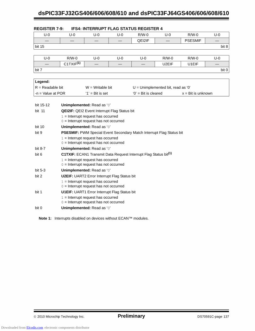
2010 Microchip Technology Inc. Preliminary DS70591C-page 137
dsPIC33FJ32GS406/606/608/610 and dsPIC33FJ64GS406/606/608/610
REGISTER 7-9: IFS4: INTERRUPT FLAG STATUS REGISTER 4
U-0 U-0 U-0 U-0 R/W-0 U-0 R/W-0 U-0
— — — — QEI2IF — PSESMIF —
bit 15 bit 8
U-0 R/W-0 U-0 U-0 U-0 R/W-0 R/W-0 U-0
— C1TXIF(1) — — — U2EIF U1EIF —
bit 7 bit 0
Legend:
R = Readable bit W = Writable bit U = Unimplemented bit, read as ‘0’
-n = Value at POR ‘1’ = Bit is set ‘0’ = Bit is cleared x = Bit is unknown
bit 15-12 Unimplemented: Read as ‘0’
bit 11 QEI2IF: QEI2 Event Interrupt Flag Status bit
1 = Interrupt request has occurred0 = Interrupt request has not occurred
bit 10 Unimplemented: Read as ‘0’
bit 9 PSESMIF: PWM Special Event Secondary Match Interrupt Flag Status bit
1 = Interrupt request has occurred0 = Interrupt request has not occurred
bit 8-7 Unimplemented: Read as ‘0’
bit 6 C1TXIF: ECAN1 Transmit Data Request Interrupt Flag Status bit(1)
1 = Interrupt request has occurred0 = Interrupt request has not occurred
bit 5-3 Unimplemented: Read as ‘0’
bit 2 U2EIF: UART2 Error Interrupt Flag Status bit
1 = Interrupt request has occurred0 = Interrupt request has not occurred
bit 1 U1EIF: UART1 Error Interrupt Flag Status bit
1 = Interrupt request has occurred0 = Interrupt request has not occurred
bit 0 Unimplemented: Read as ‘0’
Note 1: Interrupts disabled on devices without ECAN™ modules.
Downloaded from Elcodis.com electronic components distributor

dsPIC33FJ32GS406/606/608/610 and dsPIC33FJ64GS406/606/608/610
DS70591C-page 138 Preliminary 2010 Microchip Technology Inc.
REGISTER 7-10: IFS5: INTERRUPT FLAG STATUS REGISTER 5
R/W-0 R/W-0 R/W-0 U-0 U-0 U-0 U-0 U-0
PWM2IF PWM1IF ADCP12IF — — — — —
bit 15 bit 8
U-0 U-0 U-0 R/W-0 R/W-0 R/W-0 R/W-0 U-0
— — — ADCP11IF ADCP10IF ADCP9IF ADCP8IF —
bit 7 bit 0
Legend:
R = Readable bit W = Writable bit U = Unimplemented bit, read as ‘0’
-n = Value at POR ‘1’ = Bit is set ‘0’ = Bit is cleared x = Bit is unknown
bit 15 PWM2IF: PWM2 Interrupt Flag Status bit
1 = Interrupt request has occurred0 = Interrupt request has not occurred
bit 14 PWM1IF: PWM1 Interrupt Flag Status bit
1 = Interrupt request has occurred0 = Interrupt request has not occurred
bit 13 ADCP12IF: ADC Pair 12 Conversion Done Interrupt Flag Status bit
1 = Interrupt request has occurred0 = Interrupt request has not occurred
bit 12-5 Unimplemented: Read as ‘0’
bit 4 ADCP11IF: ADC Pair 11 Conversion Done Interrupt Flag Status bit
1 = Interrupt request has occurred0 = Interrupt request has not occurred
bit 3 ADCP10IF: ADC Pair 10 Conversion Done Interrupt Flag Status bit
1 = Interrupt request has occurred0 = Interrupt request has not occurred
bit 2 ADCP9IF: ADC Pair 9 Conversion Done Interrupt Flag Status bit
1 = Interrupt request has occurred0 = Interrupt request has not occurred
bit 1 ADCP8IF: ADC Pair 8 Conversion Done Interrupt Flag Status bit
1 = Interrupt request has occurred0 = Interrupt request has not occurred
bit 0 Unimplemented: Read as ‘0’
Downloaded from Elcodis.com electronic components distributor
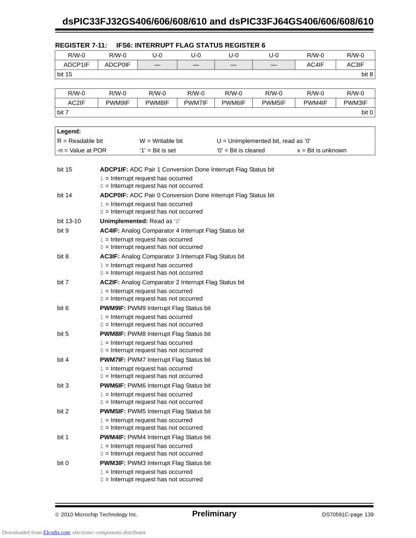
2010 Microchip Technology Inc. Preliminary DS70591C-page 139
dsPIC33FJ32GS406/606/608/610 and dsPIC33FJ64GS406/606/608/610
REGISTER 7-11: IFS6: INTERRUPT FLAG STATUS REGISTER 6
R/W-0 R/W-0 U-0 U-0 U-0 U-0 R/W-0 R/W-0
ADCP1IF ADCP0IF — — — — AC4IF AC3IF
bit 15 bit 8
R/W-0 R/W-0 R/W-0 R/W-0 R/W-0 R/W-0 R/W-0 R/W-0
AC2IF PWM9IF PWM8IF PWM7IF PWM6IF PWM5IF PWM4IF PWM3IF
bit 7 bit 0
Legend:
R = Readable bit W = Writable bit U = Unimplemented bit, read as ‘0’
-n = Value at POR ‘1’ = Bit is set ‘0’ = Bit is cleared x = Bit is unknown
bit 15 ADCP1IF: ADC Pair 1 Conversion Done Interrupt Flag Status bit
1 = Interrupt request has occurred0 = Interrupt request has not occurred
bit 14 ADCP0IF: ADC Pair 0 Conversion Done Interrupt Flag Status bit
1 = Interrupt request has occurred0 = Interrupt request has not occurred
bit 13-10 Unimplemented: Read as ‘0’
bit 9 AC4IF: Analog Comparator 4 Interrupt Flag Status bit
1 = Interrupt request has occurred0 = Interrupt request has not occurred
bit 8 AC3IF: Analog Comparator 3 Interrupt Flag Status bit
1 = Interrupt request has occurred0 = Interrupt request has not occurred
bit 7 AC2IF: Analog Comparator 2 Interrupt Flag Status bit
1 = Interrupt request has occurred0 = Interrupt request has not occurred
bit 6 PWM9IF: PWM9 Interrupt Flag Status bit
1 = Interrupt request has occurred0 = Interrupt request has not occurred
bit 5 PWM8IF: PWM8 Interrupt Flag Status bit
1 = Interrupt request has occurred0 = Interrupt request has not occurred
bit 4 PWM7IF: PWM7 Interrupt Flag Status bit
1 = Interrupt request has occurred0 = Interrupt request has not occurred
bit 3 PWM6IF: PWM6 Interrupt Flag Status bit
1 = Interrupt request has occurred0 = Interrupt request has not occurred
bit 2 PWM5IF: PWM5 Interrupt Flag Status bit
1 = Interrupt request has occurred0 = Interrupt request has not occurred
bit 1 PWM4IF: PWM4 Interrupt Flag Status bit
1 = Interrupt request has occurred0 = Interrupt request has not occurred
bit 0 PWM3IF: PWM3 Interrupt Flag Status bit
1 = Interrupt request has occurred0 = Interrupt request has not occurred
Downloaded from Elcodis.com electronic components distributor

dsPIC33FJ32GS406/606/608/610 and dsPIC33FJ64GS406/606/608/610
DS70591C-page 140 Preliminary 2010 Microchip Technology Inc.
REGISTER 7-12: IFS7: INTERRUPT FLAG STATUS REGISTER 7
U-0 U-0 U-0 U-0 U-0 U-0 U-0 U-0
— — — — — — — —
bit 15 bit 8
U-0 U-0 R/W-0 R/W-0 R/W-0 R/W-0 R/W-0 R/W-0
— — ADCP7IF ADCP6IF ADCP5IF ADCP4IF ADCP3IF ADCP2IF
bit 7 bit 0
Legend:
R = Readable bit W = Writable bit U = Unimplemented bit, read as ‘0’
-n = Value at POR ‘1’ = Bit is set ‘0’ = Bit is cleared x = Bit is unknown
bit 15-6 Unimplemented: Read as ‘0’
bit 5 ADCP7IF: ADC Pair 7 Conversion Done Interrupt Flag Status bit
1 = Interrupt request has occurred0 = Interrupt request has not occurred
bit 4 ADCP6IF: ADC Pair 6 Conversion Done Interrupt Flag Status bit
1 = Interrupt request has occurred0 = Interrupt request has not occurred
bit 3 ADCP5IF: ADC Pair 5 Conversion Done Interrupt Flag Status bit
1 = Interrupt request has occurred0 = Interrupt request has not occurred
bit 2 ADCP4IF: ADC Pair 4 Conversion Done Interrupt Flag Status bit
1 = Interrupt request has occurred0 = Interrupt request has not occurred
bit 1 ADCP3IF: ADC Pair 3 Conversion Done Interrupt Flag Status bit
1 = Interrupt request has occurred0 = Interrupt request has not occurred
bit 0 ADCP2IF: ADC Pair 2 Conversion Done Interrupt Flag Status bit
1 = Interrupt request has occurred0 = Interrupt request has not occurred
Downloaded from Elcodis.com electronic components distributor
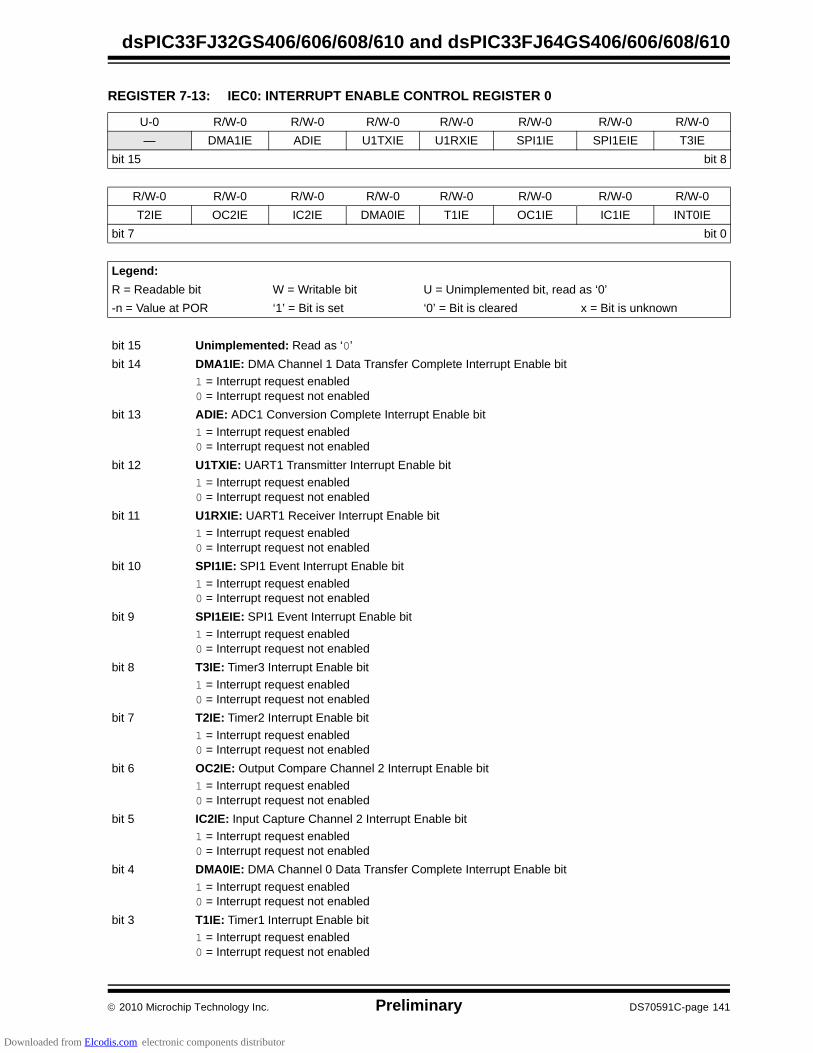
2010 Microchip Technology Inc. Preliminary DS70591C-page 141
dsPIC33FJ32GS406/606/608/610 and dsPIC33FJ64GS406/606/608/610
REGISTER 7-13: IEC0: INTERRUPT ENABLE CONTROL REGISTER 0
U-0 R/W-0 R/W-0 R/W-0 R/W-0 R/W-0 R/W-0 R/W-0
— DMA1IE ADIE U1TXIE U1RXIE SPI1IE SPI1EIE T3IE
bit 15 bit 8
R/W-0 R/W-0 R/W-0 R/W-0 R/W-0 R/W-0 R/W-0 R/W-0
T2IE OC2IE IC2IE DMA0IE T1IE OC1IE IC1IE INT0IE
bit 7 bit 0
Legend:
R = Readable bit W = Writable bit U = Unimplemented bit, read as ‘0’
-n = Value at POR ‘1’ = Bit is set ‘0’ = Bit is cleared x = Bit is unknown
bit 15 Unimplemented: Read as ‘0’
bit 14 DMA1IE: DMA Channel 1 Data Transfer Complete Interrupt Enable bit
1 = Interrupt request enabled0 = Interrupt request not enabled
bit 13 ADIE: ADC1 Conversion Complete Interrupt Enable bit
1 = Interrupt request enabled0 = Interrupt request not enabled
bit 12 U1TXIE: UART1 Transmitter Interrupt Enable bit
1 = Interrupt request enabled0 = Interrupt request not enabled
bit 11 U1RXIE: UART1 Receiver Interrupt Enable bit
1 = Interrupt request enabled0 = Interrupt request not enabled
bit 10 SPI1IE: SPI1 Event Interrupt Enable bit
1 = Interrupt request enabled0 = Interrupt request not enabled
bit 9 SPI1EIE: SPI1 Event Interrupt Enable bit
1 = Interrupt request enabled0 = Interrupt request not enabled
bit 8 T3IE: Timer3 Interrupt Enable bit
1 = Interrupt request enabled0 = Interrupt request not enabled
bit 7 T2IE: Timer2 Interrupt Enable bit
1 = Interrupt request enabled0 = Interrupt request not enabled
bit 6 OC2IE: Output Compare Channel 2 Interrupt Enable bit
1 = Interrupt request enabled0 = Interrupt request not enabled
bit 5 IC2IE: Input Capture Channel 2 Interrupt Enable bit
1 = Interrupt request enabled0 = Interrupt request not enabled
bit 4 DMA0IE: DMA Channel 0 Data Transfer Complete Interrupt Enable bit
1 = Interrupt request enabled0 = Interrupt request not enabled
bit 3 T1IE: Timer1 Interrupt Enable bit
1 = Interrupt request enabled0 = Interrupt request not enabled
Downloaded from Elcodis.com electronic components distributor
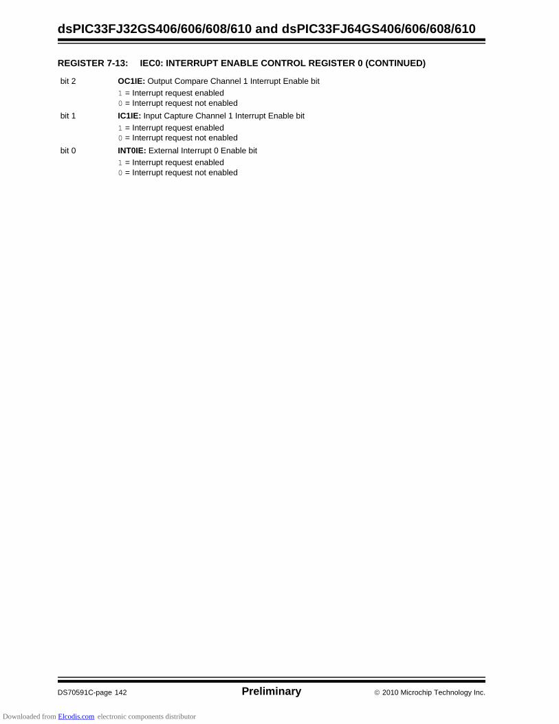
dsPIC33FJ32GS406/606/608/610 and dsPIC33FJ64GS406/606/608/610
DS70591C-page 142 Preliminary 2010 Microchip Technology Inc.
bit 2 OC1IE: Output Compare Channel 1 Interrupt Enable bit
1 = Interrupt request enabled0 = Interrupt request not enabled
bit 1 IC1IE: Input Capture Channel 1 Interrupt Enable bit
1 = Interrupt request enabled0 = Interrupt request not enabled
bit 0 INT0IE: External Interrupt 0 Enable bit
1 = Interrupt request enabled0 = Interrupt request not enabled
REGISTER 7-13: IEC0: INTERRUPT ENABLE CONTROL REGISTER 0 (CONTINUED)
Downloaded from Elcodis.com electronic components distributor
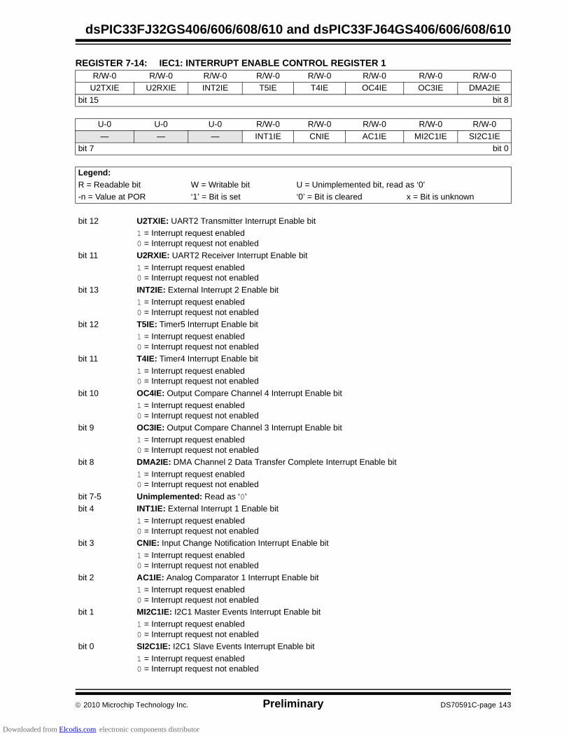
2010 Microchip Technology Inc. Preliminary DS70591C-page 143
dsPIC33FJ32GS406/606/608/610 and dsPIC33FJ64GS406/606/608/610
REGISTER 7-14: IEC1: INTERRUPT ENABLE CONTROL REGISTER 1R/W-0 R/W-0 R/W-0 R/W-0 R/W-0 R/W-0 R/W-0 R/W-0
U2TXIE U2RXIE INT2IE T5IE T4IE OC4IE OC3IE DMA2IE
bit 15 bit 8
U-0 U-0 U-0 R/W-0 R/W-0 R/W-0 R/W-0 R/W-0
— — — INT1IE CNIE AC1IE MI2C1IE SI2C1IE
bit 7 bit 0
Legend:
R = Readable bit W = Writable bit U = Unimplemented bit, read as ‘0’
-n = Value at POR ‘1’ = Bit is set ‘0’ = Bit is cleared x = Bit is unknown
bit 12 U2TXIE: UART2 Transmitter Interrupt Enable bit
1 = Interrupt request enabled0 = Interrupt request not enabled
bit 11 U2RXIE: UART2 Receiver Interrupt Enable bit
1 = Interrupt request enabled0 = Interrupt request not enabled
bit 13 INT2IE: External Interrupt 2 Enable bit
1 = Interrupt request enabled0 = Interrupt request not enabled
bit 12 T5IE: Timer5 Interrupt Enable bit
1 = Interrupt request enabled0 = Interrupt request not enabled
bit 11 T4IE: Timer4 Interrupt Enable bit
1 = Interrupt request enabled0 = Interrupt request not enabled
bit 10 OC4IE: Output Compare Channel 4 Interrupt Enable bit
1 = Interrupt request enabled0 = Interrupt request not enabled
bit 9 OC3IE: Output Compare Channel 3 Interrupt Enable bit
1 = Interrupt request enabled0 = Interrupt request not enabled
bit 8 DMA2IE: DMA Channel 2 Data Transfer Complete Interrupt Enable bit
1 = Interrupt request enabled0 = Interrupt request not enabled
bit 7-5 Unimplemented: Read as ‘0’
bit 4 INT1IE: External Interrupt 1 Enable bit
1 = Interrupt request enabled0 = Interrupt request not enabled
bit 3 CNIE: Input Change Notification Interrupt Enable bit
1 = Interrupt request enabled0 = Interrupt request not enabled
bit 2 AC1IE: Analog Comparator 1 Interrupt Enable bit
1 = Interrupt request enabled0 = Interrupt request not enabled
bit 1 MI2C1IE: I2C1 Master Events Interrupt Enable bit
1 = Interrupt request enabled0 = Interrupt request not enabled
bit 0 SI2C1IE: I2C1 Slave Events Interrupt Enable bit
1 = Interrupt request enabled0 = Interrupt request not enabled
Downloaded from Elcodis.com electronic components distributor

dsPIC33FJ32GS406/606/608/610 and dsPIC33FJ64GS406/606/608/610
DS70591C-page 144 Preliminary 2010 Microchip Technology Inc.
REGISTER 7-15: IEC2: INTERRUPT ENABLE CONTROL REGISTER 2
U-0 U-0 U-0 U-0 U-0 U-0 U-0 U-0
— — — — — — — —
bit 15 bit 8
U-0 R/W-0 R/W-0 R/W-0 R/W-0 R/W-0 R/W-0 R/W-0
— IC4IE IC3IE DMA3IE C1IE(1) C1RXIE(1) SPI2IE SPI2EIE
bit 7 bit 0
Legend:
R = Readable bit W = Writable bit U = Unimplemented bit, read as ‘0’
-n = Value at POR ‘1’ = Bit is set ‘0’ = Bit is cleared x = Bit is unknown
bit 15-7 Unimplemented: Read as ‘0’
bit 6 IC4IE: Input Capture Channel 4 Interrupt Enable bit
1 = Interrupt request enabled0 = Interrupt request not enabled
bit 5 IC3IE: Input Capture Channel 3 Interrupt Enable bit
1 = Interrupt request enabled0 = Interrupt request not enabled
bit 4 DMA3IE: DMA Channel 3 Data Transfer Complete Interrupt Enable bit
1 = Interrupt request enabled0 = Interrupt request has enabled
bit 3 C1IE: ECAN1 Event Interrupt Enable bit(1)
1 = Interrupt request enabled0 = Interrupt request not enabled
bit 2 C1RXIE: ECAN1 Receive Data Ready Interrupt Enable bit(1)
1 = Interrupt request enabled0 = Interrupt request not enabled
bit 1 SPI2IE: SPI2 Event Interrupt Enable bit
1 = Interrupt request enabled0 = Interrupt request not enabled
bit 0 SPI2EIE: SPI2 Error Interrupt Enable bit
1 = Interrupt request enabled0 = Interrupt request not enabled
Note 1: Interrupts disabled on devices without ECAN™ modules
Downloaded from Elcodis.com electronic components distributor

2010 Microchip Technology Inc. Preliminary DS70591C-page 145
dsPIC33FJ32GS406/606/608/610 and dsPIC33FJ64GS406/606/608/610
REGISTER 7-16: IEC3: INTERRUPT ENABLE CONTROL REGISTER 3
U-0 U-0 U-0 U-0 U-0 R/W-0 R/W-0 U-0
— — — — — QEI1IE PSEMIE —
bit 15 bit 8
U-0 R/W-0 R/W-0 U-0 U-0 R/W-0 R/W-0 U-0
— INT4IE INT3EI — — MI2C2IE SI2C2IE —
bit 7 bit 0
Legend:
R = Readable bit W = Writable bit U = Unimplemented bit, read as ‘0’
-n = Value at POR ‘1’ = Bit is set ‘0’ = Bit is cleared x = Bit is unknown
bit 15-11 Unimplemented: Read as ‘0’
bit 10 QEI1IE: QEI1 Event Interrupt Enable bit
1 = Interrupt request enabled0 = Interrupt request not enabled
bit 9 PSEMIE: PWM Special Event Match Interrupt Enable bit
1 = Interrupt request enabled0 = Interrupt request not enabled
bit 8-7 Unimplemented: Read as ‘0’
bit 6 INT4IE: External Interrupt 4 Enable bit
1 = Interrupt request enabled0 = Interrupt request not enabled
bit 6 INT3IE: External Interrupt 3 Enable bit
1 = Interrupt request enabled0 = Interrupt request not enabled
bit 4-3 Unimplemented: Read as ‘0’
bit 2 MI2C2IE: I2C2 Master Events Interrupt Enable bit
1 = Interrupt request enabled0 = Interrupt request not enabled
bit 1 SI2C2IE: I2C2 Slave Events Interrupt Enable bit
1 = Interrupt request enabled0 = Interrupt request not enabled
bit 0 Unimplemented: Read as ‘0’
Downloaded from Elcodis.com electronic components distributor

dsPIC33FJ32GS406/606/608/610 and dsPIC33FJ64GS406/606/608/610
DS70591C-page 146 Preliminary 2010 Microchip Technology Inc.
REGISTER 7-17: IEC4: INTERRUPT ENABLE CONTROL REGISTER 4
U-0 U-0 U-0 U-0 R/W-0 U-0 R/W-0 U-0
— — — — QEI2IE — PSESMIE —
bit 15 bit 8
U-0 R/W-0 U-0 U-0 U-0 R/W-0 R/W-0 U-0
— C1TXIE(1) — — — U2EIE U1EIE —
bit 7 bit 0
Legend:
R = Readable bit W = Writable bit U = Unimplemented bit, read as ‘0’
-n = Value at POR ‘1’ = Bit is set ‘0’ = Bit is cleared x = Bit is unknown
bit 15-12 Unimplemented: Read as ‘0’
bit 11 QEI2IE: QEI2 Event Interrupt Enable bit
1 = Interrupt request enabled0 = Interrupt request not enabled
bit 10 Unimplemented: Read as ‘0’
bit 9 PSESMIE: PWM Special Event Secondary Match Error Interrupt Enable bit
1 = Interrupt request enabled0 = Interrupt request not enabled
bit 8-7 Unimplemented: Read as ‘0’
bit 6 C1TXIE: ECAN1 Transmit Data Request Interrupt Enable bit(1)
1 = Interrupt request occurred0 = Interrupt request not occurred
bit 5-3 Unimplemented: Read as ‘0’
bit 2 U2EIE: UART2 Error Interrupt Enable bit
1 = Interrupt request enabled0 = Interrupt request not enabled
bit 1 U1EIE: UART1 Error Interrupt Enable bit
1 = Interrupt request enabled0 = Interrupt request not enabled
bit 0 Unimplemented: Read as ‘0’
Note 1: Interrupts disabled on devices without ECAN™ modules.
Downloaded from Elcodis.com electronic components distributor
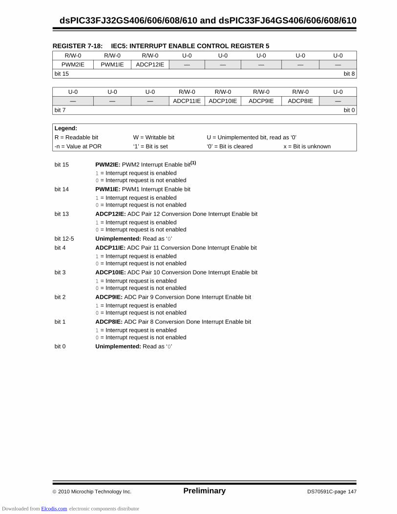
2010 Microchip Technology Inc. Preliminary DS70591C-page 147
dsPIC33FJ32GS406/606/608/610 and dsPIC33FJ64GS406/606/608/610
REGISTER 7-18: IEC5: INTERRUPT ENABLE CONTROL REGISTER 5
R/W-0 R/W-0 R/W-0 U-0 U-0 U-0 U-0 U-0
PWM2IE PWM1IE ADCP12IE — — — — —
bit 15 bit 8
U-0 U-0 U-0 R/W-0 R/W-0 R/W-0 R/W-0 U-0
— — — ADCP11IE ADCP10IE ADCP9IE ADCP8IE —
bit 7 bit 0
Legend:
R = Readable bit W = Writable bit U = Unimplemented bit, read as ‘0’
-n = Value at POR ‘1’ = Bit is set ‘0’ = Bit is cleared x = Bit is unknown
bit 15 PWM2IE: PWM2 Interrupt Enable bit(1)
1 = Interrupt request is enabled0 = Interrupt request is not enabled
bit 14 PWM1IE: PWM1 Interrupt Enable bit
1 = Interrupt request is enabled0 = Interrupt request is not enabled
bit 13 ADCP12IE: ADC Pair 12 Conversion Done Interrupt Enable bit
1 = Interrupt request is enabled0 = Interrupt request is not enabled
bit 12-5 Unimplemented: Read as ‘0’
bit 4 ADCP11IE: ADC Pair 11 Conversion Done Interrupt Enable bit
1 = Interrupt request is enabled0 = Interrupt request is not enabled
bit 3 ADCP10IE: ADC Pair 10 Conversion Done Interrupt Enable bit
1 = Interrupt request is enabled0 = Interrupt request is not enabled
bit 2 ADCP9IE: ADC Pair 9 Conversion Done Interrupt Enable bit
1 = Interrupt request is enabled0 = Interrupt request is not enabled
bit 1 ADCP8IE: ADC Pair 8 Conversion Done Interrupt Enable bit
1 = Interrupt request is enabled0 = Interrupt request is not enabled
bit 0 Unimplemented: Read as ‘0’
Downloaded from Elcodis.com electronic components distributor
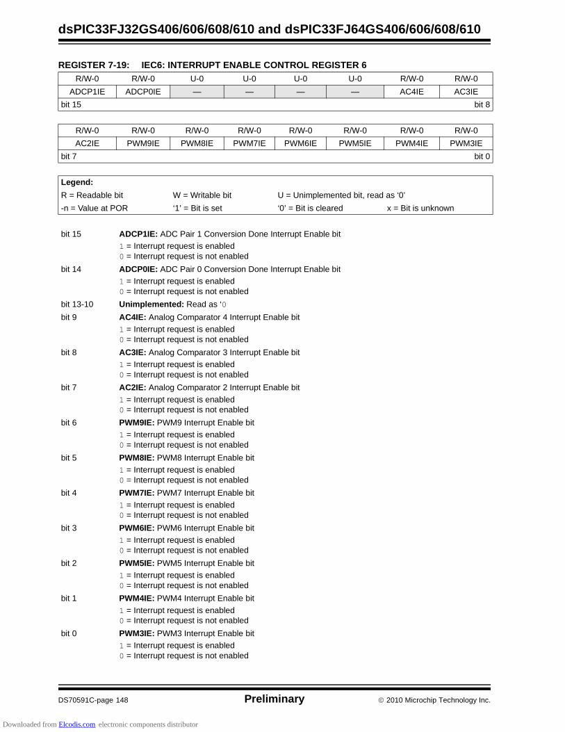
dsPIC33FJ32GS406/606/608/610 and dsPIC33FJ64GS406/606/608/610
DS70591C-page 148 Preliminary 2010 Microchip Technology Inc.
REGISTER 7-19: IEC6: INTERRUPT ENABLE CONTROL REGISTER 6
R/W-0 R/W-0 U-0 U-0 U-0 U-0 R/W-0 R/W-0
ADCP1IE ADCP0IE — — — — AC4IE AC3IE
bit 15 bit 8
R/W-0 R/W-0 R/W-0 R/W-0 R/W-0 R/W-0 R/W-0 R/W-0
AC2IE PWM9IE PWM8IE PWM7IE PWM6IE PWM5IE PWM4IE PWM3IE
bit 7 bit 0
Legend:
R = Readable bit W = Writable bit U = Unimplemented bit, read as ‘0’
-n = Value at POR ‘1’ = Bit is set ‘0’ = Bit is cleared x = Bit is unknown
bit 15 ADCP1IE: ADC Pair 1 Conversion Done Interrupt Enable bit
1 = Interrupt request is enabled0 = Interrupt request is not enabled
bit 14 ADCP0IE: ADC Pair 0 Conversion Done Interrupt Enable bit
1 = Interrupt request is enabled0 = Interrupt request is not enabled
bit 13-10 Unimplemented: Read as ‘0
bit 9 AC4IE: Analog Comparator 4 Interrupt Enable bit
1 = Interrupt request is enabled0 = Interrupt request is not enabled
bit 8 AC3IE: Analog Comparator 3 Interrupt Enable bit
1 = Interrupt request is enabled0 = Interrupt request is not enabled
bit 7 AC2IE: Analog Comparator 2 Interrupt Enable bit
1 = Interrupt request is enabled0 = Interrupt request is not enabled
bit 6 PWM9IE: PWM9 Interrupt Enable bit
1 = Interrupt request is enabled0 = Interrupt request is not enabled
bit 5 PWM8IE: PWM8 Interrupt Enable bit
1 = Interrupt request is enabled0 = Interrupt request is not enabled
bit 4 PWM7IE: PWM7 Interrupt Enable bit
1 = Interrupt request is enabled0 = Interrupt request is not enabled
bit 3 PWM6IE: PWM6 Interrupt Enable bit
1 = Interrupt request is enabled0 = Interrupt request is not enabled
bit 2 PWM5IE: PWM5 Interrupt Enable bit
1 = Interrupt request is enabled0 = Interrupt request is not enabled
bit 1 PWM4IE: PWM4 Interrupt Enable bit
1 = Interrupt request is enabled0 = Interrupt request is not enabled
bit 0 PWM3IE: PWM3 Interrupt Enable bit
1 = Interrupt request is enabled0 = Interrupt request is not enabled
Downloaded from Elcodis.com electronic components distributor
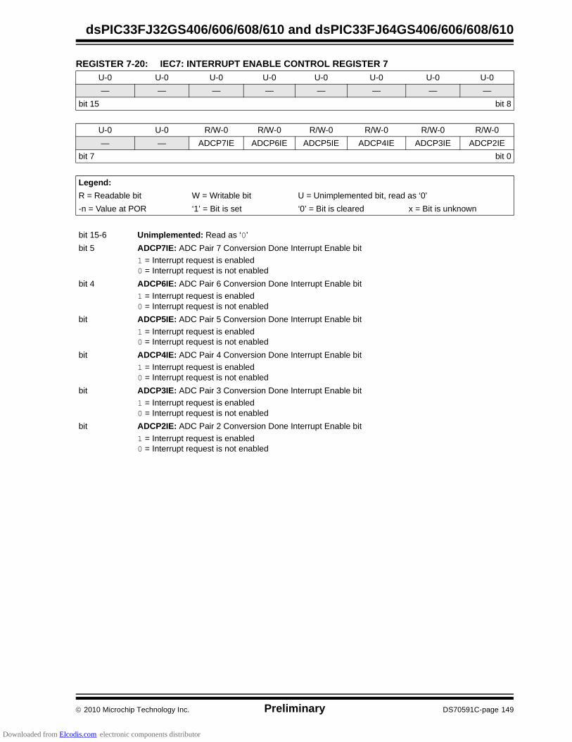
2010 Microchip Technology Inc. Preliminary DS70591C-page 149
dsPIC33FJ32GS406/606/608/610 and dsPIC33FJ64GS406/606/608/610
REGISTER 7-20: IEC7: INTERRUPT ENABLE CONTROL REGISTER 7
U-0 U-0 U-0 U-0 U-0 U-0 U-0 U-0
— — — — — — — —
bit 15 bit 8
U-0 U-0 R/W-0 R/W-0 R/W-0 R/W-0 R/W-0 R/W-0
— — ADCP7IE ADCP6IE ADCP5IE ADCP4IE ADCP3IE ADCP2IE
bit 7 bit 0
Legend:
R = Readable bit W = Writable bit U = Unimplemented bit, read as ‘0’
-n = Value at POR ‘1’ = Bit is set ‘0’ = Bit is cleared x = Bit is unknown
bit 15-6 Unimplemented: Read as ‘0’
bit 5 ADCP7IE: ADC Pair 7 Conversion Done Interrupt Enable bit
1 = Interrupt request is enabled0 = Interrupt request is not enabled
bit 4 ADCP6IE: ADC Pair 6 Conversion Done Interrupt Enable bit
1 = Interrupt request is enabled0 = Interrupt request is not enabled
bit ADCP5IE: ADC Pair 5 Conversion Done Interrupt Enable bit
1 = Interrupt request is enabled0 = Interrupt request is not enabled
bit ADCP4IE: ADC Pair 4 Conversion Done Interrupt Enable bit
1 = Interrupt request is enabled0 = Interrupt request is not enabled
bit ADCP3IE: ADC Pair 3 Conversion Done Interrupt Enable bit
1 = Interrupt request is enabled0 = Interrupt request is not enabled
bit ADCP2IE: ADC Pair 2 Conversion Done Interrupt Enable bit
1 = Interrupt request is enabled0 = Interrupt request is not enabled
Downloaded from Elcodis.com electronic components distributor
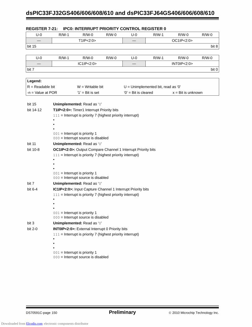
dsPIC33FJ32GS406/606/608/610 and dsPIC33FJ64GS406/606/608/610
DS70591C-page 150 Preliminary 2010 Microchip Technology Inc.
REGISTER 7-21: IPC0: INTERRUPT PRIORITY CONTROL REGISTER 0
U-0 R/W-1 R/W-0 R/W-0 U-0 R/W-1 R/W-0 R/W-0
— T1IP<2:0> — OC1IP<2:0>
bit 15 bit 8
U-0 R/W-1 R/W-0 R/W-0 U-0 R/W-1 R/W-0 R/W-0
— IC1IP<2:0> — INT0IP<2:0>
bit 7 bit 0
Legend:
R = Readable bit W = Writable bit U = Unimplemented bit, read as ‘0’
-n = Value at POR ‘1’ = Bit is set ‘0’ = Bit is cleared x = Bit is unknown
bit 15 Unimplemented: Read as ‘0’
bit 14-12 T1IP<2:0>: Timer1 Interrupt Priority bits
111 = Interrupt is priority 7 (highest priority interrupt)•••001 = Interrupt is priority 1000 = Interrupt source is disabled
bit 11 Unimplemented: Read as ‘0’
bit 10-8 OC1IP<2:0>: Output Compare Channel 1 Interrupt Priority bits
111 = Interrupt is priority 7 (highest priority interrupt)•••001 = Interrupt is priority 1000 = Interrupt source is disabled
bit 7 Unimplemented: Read as ‘0’
bit 6-4 IC1IP<2:0>: Input Capture Channel 1 Interrupt Priority bits
111 = Interrupt is priority 7 (highest priority interrupt)•••001 = Interrupt is priority 1000 = Interrupt source is disabled
bit 3 Unimplemented: Read as ‘0’
bit 2-0 INT0IP<2:0>: External Interrupt 0 Priority bits
111 = Interrupt is priority 7 (highest priority interrupt)•••001 = Interrupt is priority 1000 = Interrupt source is disabled
Downloaded from Elcodis.com electronic components distributor

2010 Microchip Technology Inc. Preliminary DS70591C-page 151
dsPIC33FJ32GS406/606/608/610 and dsPIC33FJ64GS406/606/608/610
REGISTER 7-22: IPC1: INTERRUPT PRIORITY CONTROL REGISTER 1
U-0 R/W-1 R/W-0 R/W-0 U-0 R/W-1 R/W-0 R/W-0
— T2IP<2:0> — OC2IP<2:0>
bit 15 bit 8
U-0 R/W-1 R/W-0 R/W-0 U-0 R/W-1 R/W-0 R/W-0
— IC2IP<2:0> — DMA0IP<2:0>
bit 7 bit 0
Legend:
R = Readable bit W = Writable bit U = Unimplemented bit, read as ‘0’
-n = Value at POR ‘1’ = Bit is set ‘0’ = Bit is cleared x = Bit is unknown
bit 15 Unimplemented: Read as ‘0’
bit 14-12 T2IP<2:0>: Timer2 Interrupt Priority bits
111 = Interrupt is priority 7 (highest priority interrupt)•••001 = Interrupt is priority 1000 = Interrupt source is disabled
bit 11 Unimplemented: Read as ‘0’
bit 10-8 OC2IP<2:0>: Output Compare Channel 2 Interrupt Priority bits
111 = Interrupt is priority 7 (highest priority interrupt)•••001 = Interrupt is priority 1000 = Interrupt source is disabled
bit 7 Unimplemented: Read as ‘0’
bit 6-4 IC2IP<2:0>: Input Capture Channel 2 Interrupt Priority bits
111 = Interrupt is priority 7 (highest priority interrupt)•••001 = Interrupt is priority 1000 = Interrupt source is disabled
bit 3-0 DMA0IP<2:0>: DMA Channel 0 Data Transfer Complete Interrupt Priority bits
111 = Interrupt is priority 7 (highest priority interrupt)•••001 = Interrupt is priority 1000 = Interrupt source is disabled
Downloaded from Elcodis.com electronic components distributor

dsPIC33FJ32GS406/606/608/610 and dsPIC33FJ64GS406/606/608/610
DS70591C-page 152 Preliminary 2010 Microchip Technology Inc.
REGISTER 7-23: IPC2: INTERRUPT PRIORITY CONTROL REGISTER 2
U-0 R/W-1 R/W-0 R/W-0 U-0 R/W-1 R/W-0 R/W-0
— U1RXIP<2:0> — SPI1IP<2:0>
bit 15 bit 8
U-0 R/W-1 R/W-0 R/W-0 U-0 R/W-1 R/W-0 R/W-0
— SPI1EIP<2:0> — T3IP<2:0>
bit 7 bit 0
Legend:
R = Readable bit W = Writable bit U = Unimplemented bit, read as ‘0’
-n = Value at POR ‘1’ = Bit is set ‘0’ = Bit is cleared x = Bit is unknown
bit 15 Unimplemented: Read as ‘0’
bit 14-12 U1RXIP<2:0>: UART1 Receiver Interrupt Priority bits
111 = Interrupt is priority 7 (highest priority interrupt)•••001 = Interrupt is priority 1000 = Interrupt source is disabled
bit 11 Unimplemented: Read as ‘0’
bit 10-8 SPI1IP<2:0>: SPI1 Event Interrupt Priority bits
111 = Interrupt is priority 7 (highest priority interrupt)•••001 = Interrupt is priority 1000 = Interrupt source is disabled
bit 7 Unimplemented: Read as ‘0’
bit 6-4 SPI1EIP<2:0>: SPI1 Error Interrupt Priority bits
111 = Interrupt is priority 7 (highest priority interrupt)•••001 = Interrupt is priority 1000 = Interrupt source is disabled
bit 3 Unimplemented: Read as ‘0’
bit 2-0 T3IP<2:0>: Timer3 Interrupt Priority bits
111 = Interrupt is priority 7 (highest priority interrupt)•••001 = Interrupt is priority 1000 = Interrupt source is disabled
Downloaded from Elcodis.com electronic components distributor

2010 Microchip Technology Inc. Preliminary DS70591C-page 153
dsPIC33FJ32GS406/606/608/610 and dsPIC33FJ64GS406/606/608/610
REGISTER 7-24: IPC3: INTERRUPT PRIORITY CONTROL REGISTER 3
U-0 U-0 U-0 U-0 U-0 R/W-1 R/W-0 R/W-0
— — — — — DMA1IP<2:0>
bit 15 bit 8
U-0 R/W-1 R/W-0 R/W-0 U-0 R/W-1 R/W-0 R/W-0
— ADIP<2:0> — U1TXIP<2:0>
bit 7 bit 0
Legend:
R = Readable bit W = Writable bit U = Unimplemented bit, read as ‘0’
-n = Value at POR ‘1’ = Bit is set ‘0’ = Bit is cleared x = Bit is unknown
bit 15-11 Unimplemented: Read as ‘0’
bit 10-8 DMA1IP<2:0>: DMA Channel 1 Data Transfer Complete Interrupt Priority bits
111 = Interrupt is priority 7 (highest priority interrupt)•••001 = Interrupt is priority 1000 = Interrupt source is disabled
bit 7 Unimplemented: Read as ‘0’
bit 6-4 ADIP<2:0>: ADC1 Conversion Complete Interrupt Priority bits
111 = Interrupt is priority 7 (highest priority interrupt)•••001 = Interrupt is priority 1000 = Interrupt source is disabled
bit 3 Unimplemented: Read as ‘0’
bit 2-0 U1TXIP<2:0>: UART1 Transmitter Interrupt Priority bits
111 = Interrupt is priority 7 (highest priority interrupt)•••001 = Interrupt is priority 1000 = Interrupt source is disabled
Downloaded from Elcodis.com electronic components distributor

dsPIC33FJ32GS406/606/608/610 and dsPIC33FJ64GS406/606/608/610
DS70591C-page 154 Preliminary 2010 Microchip Technology Inc.
REGISTER 7-25: IPC4: INTERRUPT PRIORITY CONTROL REGISTER 4
U-0 R/W-1 R/W-0 R/W-0 U-0 R/W-1 R/W-0 R/W-0
— CNIP<2:0> — AC1IP<2:0>
bit 15 bit 8
U-0 R/W-1 R/W-0 R/W-0 U-0 R/W-1 R/W-0 R/W-0
— MI2C1IP<2:0> — SI2C1IP<2:0>
bit 7 bit 0
Legend:
R = Readable bit W = Writable bit U = Unimplemented bit, read as ‘0’
-n = Value at POR ‘1’ = Bit is set ‘0’ = Bit is cleared x = Bit is unknown
bit 15 Unimplemented: Read as ‘0’
bit 14-12 CNIP<2:0>: Change Notification Interrupt Priority bits
111 = Interrupt is priority 7 (highest priority interrupt)•••001 = Interrupt is priority 1000 = Interrupt source is disabled
bit 11 Unimplemented: Read as ‘0’
bit 10-8 AC1IP<2:0>: Analog Comparator 1 Interrupt Priority bits
111 = Interrupt is priority 7 (highest priority interrupt)•••001 = Interrupt is priority 1000 = Interrupt source is disabled
bit 7 Unimplemented: Read as ‘0’
bit 6-4 MI2C1IP<2:0>: I2C1 Master Events Interrupt Priority bits
111 = Interrupt is priority 7 (highest priority interrupt)•••001 = Interrupt is priority 1000 = Interrupt source is disabled
bit 3 Unimplemented: Read as ‘0’
bit 2-0 SI2C1IP<2:0>: I2C1 Slave Events Interrupt Priority bits
111 = Interrupt is priority 7 (highest priority interrupt)•••001 = Interrupt is priority 1000 = Interrupt source is disabled
Downloaded from Elcodis.com electronic components distributor

2010 Microchip Technology Inc. Preliminary DS70591C-page 155
dsPIC33FJ32GS406/606/608/610 and dsPIC33FJ64GS406/606/608/610
REGISTER 7-26: IPC5: INTERRUPT PRIORITY CONTROL REGISTER 5
U-0 U-0 U-0 U-0 U-0 U-0 U-0 U-0
— — — — — — — —
bit 15 bit 8
U-0 U-0 U-0 U-0 U-0 R/W-1 R/W-0 R/W-0
— — — — — INT1IP<2:0>
bit 7 bit 0
Legend:
R = Readable bit W = Writable bit U = Unimplemented bit, read as ‘0’
-n = Value at POR ‘1’ = Bit is set ‘0’ = Bit is cleared x = Bit is unknown
bit 15-3 Unimplemented: Read as ‘0’
bit 2-0 INT1IP<2:0>: External Interrupt 1 Priority bits
111 = Interrupt is priority 7 (highest priority interrupt)•••001 = Interrupt is priority 1000 = Interrupt source is disabled
Downloaded from Elcodis.com electronic components distributor

dsPIC33FJ32GS406/606/608/610 and dsPIC33FJ64GS406/606/608/610
DS70591C-page 156 Preliminary 2010 Microchip Technology Inc.
REGISTER 7-27: IPC6: INTERRUPT PRIORITY CONTROL REGISTER 6
U-0 R/W-1 R/W-0 R/W-0 U-0 R/W-1 R/W-0 R/W-0
— T4IP<2:0> — OC4IP<2:0>
bit 15 bit 8
U-0 R/W-1 R/W-0 R/W-0 U-0 R/W-1 R/W-0 R/W-0
— OC3IP<2:0> — DMA2IP<2:0>
bit 7 bit 0
Legend:
R = Readable bit W = Writable bit U = Unimplemented bit, read as ‘0’
-n = Value at POR ‘1’ = Bit is set ‘0’ = Bit is cleared x = Bit is unknown
bit 15 Unimplemented: Read as ‘0’
bit 14-12 T4IP<2:0>: Timer4 Interrupt Priority bits
111 = Interrupt is priority 7 (highest priority interrupt)•••001 = Interrupt is priority 1000 = Interrupt source is disabled
bit 11 Unimplemented: Read as ‘0’
bit 10-8 OC4IP<2:0>: Output Compare Channel 4 Interrupt Priority bits
111 = Interrupt is priority 7 (highest priority interrupt)•••001 = Interrupt is priority 1000 = Interrupt source is disabled
bit 7 Unimplemented: Read as ‘0’
bit 6-4 OC3IP<2:0>: Output Compare Channel 3 Interrupt Priority bits
111 = Interrupt is priority 7 (highest priority interrupt)•••001 = Interrupt is priority 1000 = Interrupt source is disabled
bit 3 Unimplemented: Read as ‘0’
bit 2-0 DMA2IP<2:0>: DMA Channel 2 Data Transfer Complete Interrupt Priority bits
111 = Interrupt is priority 7 (highest priority interrupt)•••001 = Interrupt is priority 1000 = Interrupt source is disabled
Downloaded from Elcodis.com electronic components distributor

2010 Microchip Technology Inc. Preliminary DS70591C-page 157
dsPIC33FJ32GS406/606/608/610 and dsPIC33FJ64GS406/606/608/610
REGISTER 7-28: IPC7: INTERRUPT PRIORITY CONTROL REGISTER 7
U-0 R/W-1 R/W-0 R/W-0 U-0 R/W-1 R/W-0 R/W-0
— U2TXIP<2:0> — U2RXIP<2:0>
bit 15 bit 8
U-0 R/W-1 R/W-0 R/W-0 U-0 R/W-1 R/W-0 R/W-0
— INT2IP<2:0> — T5IP<2:0>
bit 7 bit 0
Legend:
R = Readable bit W = Writable bit U = Unimplemented bit, read as ‘0’
-n = Value at POR ‘1’ = Bit is set ‘0’ = Bit is cleared x = Bit is unknown
bit 15 Unimplemented: Read as ‘0’
bit 14-12 U2TXIP<2:0>: UART2 Transmitter Interrupt Priority bits
111 = Interrupt is priority 7 (highest priority interrupt)•••001 = Interrupt is priority 1000 = Interrupt source is disabled
bit 11 Unimplemented: Read as ‘0’
bit 10-8 U2RXIP<2:0>: UART2 Receiver Interrupt Priority bits
111 = Interrupt is priority 7 (highest priority interrupt)•••001 = Interrupt is priority 1000 = Interrupt source is disabled
bit 7 Unimplemented: Read as ‘0’
bit 6-4 INT2IP<2:0>: External Interrupt 2 Priority bits
111 = Interrupt is priority 7 (highest priority interrupt)•••001 = Interrupt is priority 1000 = Interrupt source is disabled
bit 3 Unimplemented: Read as ‘0’
bit 2-0 T5IP<2:0>: Timer5 Interrupt Priority bits
111 = Interrupt is priority 7 (highest priority interrupt)•••001 = Interrupt is priority 1000 = Interrupt source is disabled
Downloaded from Elcodis.com electronic components distributor

dsPIC33FJ32GS406/606/608/610 and dsPIC33FJ64GS406/606/608/610
DS70591C-page 158 Preliminary 2010 Microchip Technology Inc.
REGISTER 7-29: IPC8: INTERRUPT PRIORITY CONTROL REGISTER 8
U-0 R/W-1 R/W-0 R/W-0 U-0 R/W-1 R/W-0 R/W-0
— C1IP<2:0>(1) — C1RXIP<2:0>(1)
bit 15 bit 8
U-0 R/W-1 R/W-0 R/W-0 U-0 R/W-1 R/W-0 R/W-0
— SPI2IP<2:0> — SPI2EIP<2:0>
bit 7 bit 0
Legend:
R = Readable bit W = Writable bit U = Unimplemented bit, read as ‘0’
-n = Value at POR ‘1’ = Bit is set ‘0’ = Bit is cleared x = Bit is unknown
bit 15 Unimplemented: Read as ‘0’
bit 14-12 C1IP<2:0>: ECAN1 Event Interrupt Priority bits(1)
111 = Interrupt is priority 7 (highest priority interrupt)•••001 = Interrupt is priority 1000 = Interrupt source is disabled
bit 11 Unimplemented: Read as ‘0’
bit 10-8 C1RXIP<2:0>: ECAN1 Receive Data Ready Interrupt Priority bits(1)
111 = Interrupt is priority 7 (highest priority interrupt)•••001 = Interrupt is priority 1000 = Interrupt source is disabled
bit 7 Unimplemented: Read as ‘0’
bit 6-4 SPI2IP<2:0>: SPI2 Event Interrupt Priority bits
111 = Interrupt is priority 7 (highest priority interrupt)•••001 = Interrupt is priority 1000 = Interrupt source is disabled
bit 3 Unimplemented: Read as ‘0’
bit 2-0 SPI2EIP<2:0>: SPI2 Error Interrupt Priority bits
111 = Interrupt is priority 7 (highest priority interrupt)•••001 = Interrupt is priority 1000 = Interrupt source is disabled
Note 1: Interrupts disabled on devices without ECAN™ modules
Downloaded from Elcodis.com electronic components distributor

2010 Microchip Technology Inc. Preliminary DS70591C-page 159
dsPIC33FJ32GS406/606/608/610 and dsPIC33FJ64GS406/606/608/610
REGISTER 7-30: IPC9: INTERRUPT PRIORITY CONTROL REGISTER 9
U-0 U-0 U-0 U-0 U-0 R/W-1 R/W-0 R/W-0
— — — — — IC4IP<2:0>
bit 15 bit 8
U-0 R/W-1 R/W-0 R/W-0 U-0 R/W-1 R/W-0 R/W-0
— IC3IP<2:0> — DMA3IP<2:0>
bit 7 bit 0
Legend:
R = Readable bit W = Writable bit U = Unimplemented bit, read as ‘0’
-n = Value at POR ‘1’ = Bit is set ‘0’ = Bit is cleared x = Bit is unknown
bit 15-11 Unimplemented: Read as ‘0’
bit 10-8 IC4IP<2:0>: Input Capture Channel 4 Interrupt Priority bits
111 = Interrupt is priority 7 (highest priority interrupt)•••001 = Interrupt is priority 1000 = Interrupt source is disabled
bit 7 Unimplemented: Read as ‘0’
bit 6-4 IC3IP<2:0>: Input Capture Channel 3 Interrupt Priority bits
111 = Interrupt is priority 7 (highest priority interrupt)•••001 = Interrupt is priority 1000 = Interrupt source is disabled
bit 3 Unimplemented: Read as ‘0’
bit 2-0 DMA3IP<2:0>: DMA Channel 3 Data Transfer Complete Interrupt Priority bits
111 = Interrupt is priority 7 (highest priority interrupt)•••001 = Interrupt is priority 1000 = Interrupt source is disabled
Downloaded from Elcodis.com electronic components distributor

dsPIC33FJ32GS406/606/608/610 and dsPIC33FJ64GS406/606/608/610
DS70591C-page 160 Preliminary 2010 Microchip Technology Inc.
REGISTER 7-31: IPC12: INTERRUPT PRIORITY CONTROL REGISTER 12
U-0 U-0 U-0 U-0 U-0 R/W-1 R/W-0 R/W-0
— — — — — MI2C2IP<2:0>
bit 15 bit 8
U-0 R/W-1 R/W-0 R/W-0 U-0 U-0 U-0 U-0
— SI2C2IP<2:0> — — — —
bit 7 bit 0
Legend:
R = Readable bit W = Writable bit U = Unimplemented bit, read as ‘0’
-n = Value at POR ‘1’ = Bit is set ‘0’ = Bit is cleared x = Bit is unknown
bit 15-11 Unimplemented: Read as ‘0’
bit 10-8 MI2C2IP<2:0>: I2C2 Master Events Interrupt Priority bits
111 = Interrupt is priority 7 (highest priority interrupt)•••001 = Interrupt is priority 1000 = Interrupt source is disabled
bit 7 Unimplemented: Read as ‘0’
bit 6-4 SI2C2IP<2:0>: I2C2 Slave Events Interrupt Priority bits
111 = Interrupt is priority 7 (highest priority interrupt)•••001 = Interrupt is priority 1000 = Interrupt source is disabled
bit 3-0 Unimplemented: Read as ‘0’
Downloaded from Elcodis.com electronic components distributor

2010 Microchip Technology Inc. Preliminary DS70591C-page 161
dsPIC33FJ32GS406/606/608/610 and dsPIC33FJ64GS406/606/608/610
REGISTER 7-32: IPC13: INTERRUPT PRIORITY CONTROL REGISTER 13
U-0 U-0 U-0 U-0 U-0 R/W-1 R/W-0 R/W-0
— — — — — INT4IP<2:0>
bit 15 bit 8
U-0 R/W-1 R/W-0 R/W-0 U-0 U-0 U-0 U-0
— INT3IP<2:0> — — — —
bit 7 bit 0
Legend:
R = Readable bit W = Writable bit U = Unimplemented bit, read as ‘0’
-n = Value at POR ‘1’ = Bit is set ‘0’ = Bit is cleared x = Bit is unknown
bit 15-11 Unimplemented: Read as ‘0’
bit 10-8 INT4IP<2:0>: External Interrupt 4 Priority bits
111 = Interrupt is priority 7 (highest priority interrupt)•••001 = Interrupt is priority 1000 = Interrupt source is disabled
bit 7 Unimplemented: Read as ‘0’
bit 6-4 INT3IP<2:0>: External Interrupt 3 Priority bits
111 = Interrupt is priority 7 (highest priority interrupt)•••001 = Interrupt is priority 1000 = Interrupt source is disabled
bit 3-0 Unimplemented: Read as ‘0’
Downloaded from Elcodis.com electronic components distributor
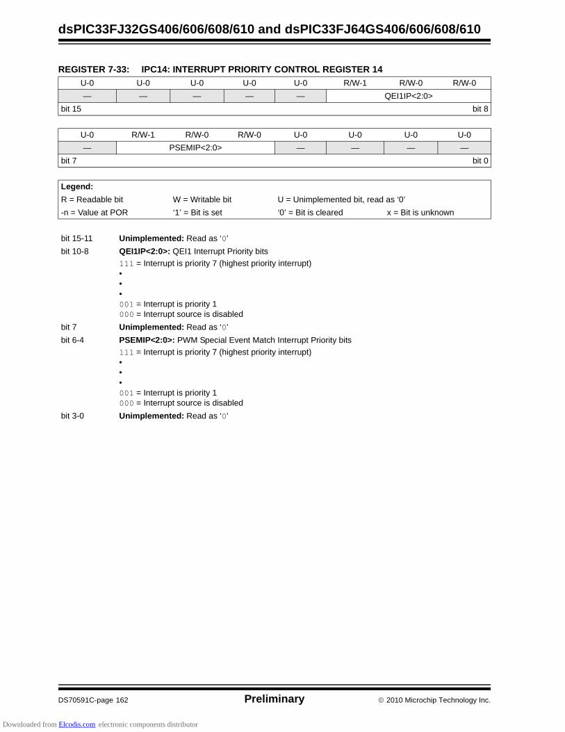
dsPIC33FJ32GS406/606/608/610 and dsPIC33FJ64GS406/606/608/610
DS70591C-page 162 Preliminary 2010 Microchip Technology Inc.
REGISTER 7-33: IPC14: INTERRUPT PRIORITY CONTROL REGISTER 14
U-0 U-0 U-0 U-0 U-0 R/W-1 R/W-0 R/W-0
— — — — — QEI1IP<2:0>
bit 15 bit 8
U-0 R/W-1 R/W-0 R/W-0 U-0 U-0 U-0 U-0
— PSEMIP<2:0> — — — —
bit 7 bit 0
Legend:
R = Readable bit W = Writable bit U = Unimplemented bit, read as ‘0’
-n = Value at POR ‘1’ = Bit is set ‘0’ = Bit is cleared x = Bit is unknown
bit 15-11 Unimplemented: Read as ‘0’
bit 10-8 QEI1IP<2:0>: QEI1 Interrupt Priority bits
111 = Interrupt is priority 7 (highest priority interrupt)•••001 = Interrupt is priority 1000 = Interrupt source is disabled
bit 7 Unimplemented: Read as ‘0’
bit 6-4 PSEMIP<2:0>: PWM Special Event Match Interrupt Priority bits
111 = Interrupt is priority 7 (highest priority interrupt)•••001 = Interrupt is priority 1000 = Interrupt source is disabled
bit 3-0 Unimplemented: Read as ‘0’
Downloaded from Elcodis.com electronic components distributor

2010 Microchip Technology Inc. Preliminary DS70591C-page 163
dsPIC33FJ32GS406/606/608/610 and dsPIC33FJ64GS406/606/608/610
REGISTER 7-34: IPC16: INTERRUPT PRIORITY CONTROL REGISTER 16
U-0 U-0 U-0 U-0 U-0 R/W-1 R/W-0 R/W-0
— — — — — U2EIP<2:0>
bit 15 bit 8
U-0 R/W-1 R/W-0 R/W-0 U-0 U-0 U-0 U-0
— U1EIP<2:0> — — — —
bit 7 bit 0
Legend:
R = Readable bit W = Writable bit U = Unimplemented bit, read as ‘0’
-n = Value at POR ‘1’ = Bit is set ‘0’ = Bit is cleared x = Bit is unknown
bit 15-11 Unimplemented: Read as ‘0’
bit 10-8 U2EIP<2:0>: UART2 Error Interrupt Priority bits
111 = Interrupt is priority 7 (highest priority interrupt)•••001 = Interrupt is priority 1000 = Interrupt source is disabled
bit 7 Unimplemented: Read as ‘0’
bit 6-4 U1EIP<2:0>: UART1 Error Interrupt Priority bits
111 = Interrupt is priority 7 (highest priority interrupt)•••001 = Interrupt is priority 1000 = Interrupt source is disabled
bit 3-0 Unimplemented: Read as ‘0’
Downloaded from Elcodis.com electronic components distributor

dsPIC33FJ32GS406/606/608/610 and dsPIC33FJ64GS406/606/608/610
DS70591C-page 164 Preliminary 2010 Microchip Technology Inc.
REGISTER 7-35: IPC17: INTERRUPT PRIORITY CONTROL REGISTER 17
U-0 U-0 U-0 U-0 U-0 R/W-1 R/W-0 R/W-0
— — — — — C1TXIP<2:0>(1)
bit 15 bit 8
U-0 U-0 U-0 U-0 U-0 U-0 U-0 U-0
— — — — — — — —
bit 7 bit 0
Legend:
R = Readable bit W = Writable bit U = Unimplemented bit, read as ‘0’
-n = Value at POR ‘1’ = Bit is set ‘0’ = Bit is cleared x = Bit is unknown
bit 15-11 Unimplemented: Read as ‘0’
bit 10-8 C1TXIP<2:0>: ECAN1 Transmit Data Request Interrupt Priority bits(1)
111 = Interrupt is priority 7 (highest priority interrupt)•••001 = Interrupt is priority 1000 = Interrupt source is disabled
bit 7-0 Unimplemented: Read as ‘0’
Note 1: Interrupts disabled on devices without ECAN™ modules
Downloaded from Elcodis.com electronic components distributor

2010 Microchip Technology Inc. Preliminary DS70591C-page 165
dsPIC33FJ32GS406/606/608/610 and dsPIC33FJ64GS406/606/608/610
REGISTER 7-36: IPC18: INTERRUPT PRIORITY CONTROL REGISTER 18
U-0 R/W-1 R/W-0 R/W-0 U-0 U-0 U-0 U-0
— QEI2IP<2:0> — — — —
bit 15 bit 8
U-0 R/W-1 R/W-0 R/W-0 U-0 U-0 U-0 U-0
— PSESMIP<2:0> — — — —
bit 7 bit 0
Legend:
R = Readable bit W = Writable bit U = Unimplemented bit, read as ‘0’
-n = Value at POR ‘1’ = Bit is set ‘0’ = Bit is cleared x = Bit is unknown
bit 15 Unimplemented: Read as ‘0’
bit 14-12 QEI2IP<2:0>: QEI2 Interrupt Priority bits
111 = Interrupt is priority 7 (highest priority interrupt)•••001 = Interrupt is priority 1000 = Interrupt source is disabled
bit 11-7 Unimplemented: Read as ‘0’
bit 6-4 PSESMIP<2:0>: PWM Special Event Secondary Match Interrupt Priority bits
111 = Interrupt is priority 7 (highest priority interrupt)•••001 = Interrupt is priority 1000 = Interrupt source is disabled
bit 3-0 Unimplemented: Read as ‘0’
Downloaded from Elcodis.com electronic components distributor

dsPIC33FJ32GS406/606/608/610 and dsPIC33FJ64GS406/606/608/610
DS70591C-page 166 Preliminary 2010 Microchip Technology Inc.
REGISTER 7-37: IPC20: INTERRUPT PRIORITY CONTROL REGISTER 20
U-0 R/W-1 R/W-0 R/W-0 U-0 R/W-1 R/W-0 R/W-0
— ADCP10IP<2:0> — ADCP9IP<2:0>
bit 15 bit 8
U-0 R/W-1 R/W-0 R/W-0 U-0 U-0 U-0 U-0
— ADCP8IP<2:0> — — — —
bit 7 bit 0
Legend:
R = Readable bit W = Writable bit U = Unimplemented bit, read as ‘0’
-n = Value at POR ‘1’ = Bit is set ‘0’ = Bit is cleared x = Bit is unknown
bit 15 Unimplemented: Read as ‘0’
bit 14-12 ADCP10IP<2:0>: ADC Pair 10 Conversion Done Interrupt 1 Priority bits
111 = Interrupt is priority 7 (highest priority interrupt)•••001 = Interrupt is priority 1000 = Interrupt source is disabled
bit 11 Unimplemented: Read as ‘0’
bit 10-8 ADCP9IP<2:0>: ADC Pair 9 Conversion Done Interrupt 1 Priority bits
111 = Interrupt is priority 7 (highest priority interrupt)•••001 = Interrupt is priority 1000 = Interrupt source is disabled
bit 7 Unimplemented: Read as ‘0’
bit 6-4 ADCP8IP<2:0>: ADC Pair 8 Conversion Done Interrupt 1 Priority bits
111 = Interrupt is priority 7 (highest priority interrupt)•••001 = Interrupt is priority 1000 = Interrupt source is disabled
bit 3-0 Unimplemented: Read as ‘0’
Downloaded from Elcodis.com electronic components distributor

2010 Microchip Technology Inc. Preliminary DS70591C-page 167
dsPIC33FJ32GS406/606/608/610 and dsPIC33FJ64GS406/606/608/610
REGISTER 7-38: IPC21: INTERRUPT PRIORITY CONTROL REGISTER 21
U-0 U-0 U-0 U-0 U-0 U-0 U-0 U-0
— — — — — — — —
bit 15 bit 8
U-0 R/W-1 R/W-0 R/W-0 U-0 R/W-1 R/W-0 R/W-0
— ADCP12IP<2:0> — ADCP11IP<2:0>
bit 7 bit 0
Legend:
R = Readable bit W = Writable bit U = Unimplemented bit, read as ‘0’
-n = Value at POR ‘1’ = Bit is set ‘0’ = Bit is cleared x = Bit is unknown
bit 15-7 Unimplemented: Read as ‘0’
bit 6-4 ADCP12IP<2:0>: ADC Pair 12 Conversion Done Interrupt 1 Priority bits
111 = Interrupt is priority 7 (highest priority interrupt)•••001 = Interrupt is priority 1000 = Interrupt source is disabled
bit 3 Unimplemented: Read as ‘0’
bit 2-0 ADCP11IP<2:0>: ADC Pair 11 Conversion Done Interrupt 1 Priority bits
111 = Interrupt is priority 7 (highest priority interrupt)•••001 = Interrupt is priority 1000 = Interrupt source is disabled
Downloaded from Elcodis.com electronic components distributor
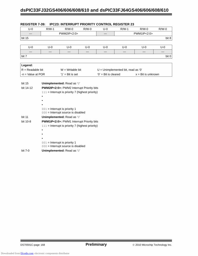
dsPIC33FJ32GS406/606/608/610 and dsPIC33FJ64GS406/606/608/610
DS70591C-page 168 Preliminary 2010 Microchip Technology Inc.
REGISTER 7-39: IPC23: INTERRUPT PRIORITY CONTROL REGISTER 23
U-0 R/W-1 R/W-0 R/W-0 U-0 R/W-1 R/W-0 R/W-0
— PWM2IP<2:0> — PWM1IP<2:0>
bit 15 bit 8
U-0 U-0 U-0 U-0 U-0 U-0 U-0 U-0
— — — — — — — —
bit 7 bit 0
Legend:
R = Readable bit W = Writable bit U = Unimplemented bit, read as ‘0’
-n = Value at POR ‘1’ = Bit is set ‘0’ = Bit is cleared x = Bit is unknown
bit 15 Unimplemented: Read as ‘0’
bit 14-12 PWM2IP<2:0>: PWM2 Interrupt Priority bits
111 = Interrupt is priority 7 (highest priority)
•
•
•
001 = Interrupt is priority 1000 = Interrupt source is disabled
bit 11 Unimplemented: Read as ‘0’
bit 10-8 PWM1IP<2:0>: PWM1 Interrupt Priority bits
111 = Interrupt is priority 7 (highest priority)
•
•
•
001 = Interrupt is priority 1000 = Interrupt source is disabled
bit 7-0 Unimplemented: Read as ‘0’
Downloaded from Elcodis.com electronic components distributor

2010 Microchip Technology Inc. Preliminary DS70591C-page 169
dsPIC33FJ32GS406/606/608/610 and dsPIC33FJ64GS406/606/608/610
REGISTER 7-40: IPC24: INTERRUPT PRIORITY CONTROL REGISTER 24
U-0 R/W-1 R/W-0 R/W-0 U-0 R/W-1 R/W-0 R/W-0
— PWM6IP<2:0> — PWM5IP<2:0>
bit 15 bit 8
U-0 R/W-1 R/W-0 R/W-0 U-0 R/W-1 R/W-0 R/W-0
— PWM4IP<2:0> — PWM3IP<2:0>
bit 7 bit 0
Legend:
R = Readable bit W = Writable bit U = Unimplemented bit, read as ‘0’
-n = Value at POR ‘1’ = Bit is set ‘0’ = Bit is cleared x = Bit is unknown
bit 15 Unimplemented: Read as ‘0’
bit 14-12 PWM6IP<2:0>: PWM6 Interrupt Priority bits
111 = Interrupt is priority 7 (highest priority)
•
•
•
001 = Interrupt is priority 1000 = Interrupt source is disabled
bit 11 Unimplemented: Read as ‘0’
bit 10-8 PWM5IP<2:0>: PWM5 Interrupt Priority bits
111 = Interrupt is priority 7 (highest priority)
•
•
•
001 = Interrupt is priority 1000 = Interrupt source is disabled
bit 7 Unimplemented: Read as ‘0’
bit 6-4 PWM4IP<2:0>: PWM4 Interrupt Priority bits
111 = Interrupt is priority 7 (highest priority)
•
•
•
001 = Interrupt is priority 1000 = Interrupt source is disabled
bit 3 Unimplemented: Read as ‘0’
bit 2-0 PWM3IP<2:0>: PWM3 Interrupt Priority bits
111 = Interrupt is priority 7 (highest priority)
•
•
•
001 = Interrupt is priority 1000 = Interrupt source is disabled
Downloaded from Elcodis.com electronic components distributor

dsPIC33FJ32GS406/606/608/610 and dsPIC33FJ64GS406/606/608/610
DS70591C-page 170 Preliminary 2010 Microchip Technology Inc.
REGISTER 7-41: IPC25: INTERRUPT PRIORITY CONTROL REGISTER 25
U-0 R/W-1 R/W-0 R/W-0 U-0 R/W-1 R/W-0 R/W-0
— AC2IP<2:0> — PWM9IP<2:0>
bit 15 bit 8
U-0 R/W-1 R/W-0 R/W-0 U-0 R/W-1 R/W-0 R/W-0
— PWM8IP<2:0> — PWM7IP<2:0>
bit 7 bit 0
Legend:
R = Readable bit W = Writable bit U = Unimplemented bit, read as ‘0’
-n = Value at POR ‘1’ = Bit is set ‘0’ = Bit is cleared x = Bit is unknown
bit 15 Unimplemented: Read as ‘0’
bit 14-12 AC2IP<2:0>: Analog Comparator 2 Interrupt Priority bits
111 = Interrupt is priority 7 (highest priority)
•
•
•
001 = Interrupt is priority 1000 = Interrupt source is disabled
bit 11 Unimplemented: Read as ‘0’
bit 10-8 PWM9IP<2:0>: PWM9 Interrupt Priority bits
111 = Interrupt is priority 7 (highest priority)
•
•
•
001 = Interrupt is priority 1000 = Interrupt source is disabled
bit 7 Unimplemented: Read as ‘0’
bit 6-4 PWM8IP<2:0>: PWM8 Interrupt Priority bits
111 = Interrupt is priority 7 (highest priority)
•
•
•
001 = Interrupt is priority 1000 = Interrupt source is disabled
bit 3 Unimplemented: Read as ‘0’
bit 2-0 PWM7IP<2:0>: PWM7 Interrupt Priority bits
111 = Interrupt is priority 7 (highest priority)
•
•
•
001 = Interrupt is priority 1000 = Interrupt source is disabled
Downloaded from Elcodis.com electronic components distributor

2010 Microchip Technology Inc. Preliminary DS70591C-page 171
dsPIC33FJ32GS406/606/608/610 and dsPIC33FJ64GS406/606/608/610
REGISTER 7-42: IPC26: INTERRUPT PRIORITY CONTROL REGISTER 26
U-0 U-0 U-0 U-0 U-0 U-0 U-0 U-0
— — — — — — — —
bit 15 bit 8
U-0 R/W-1 R/W-0 R/W-0 U-0 R/W-1 R/W-0 R/W-0
— AC4IP<2:0> — AC3IP<2:0>
bit 7 bit 0
Legend:
R = Readable bit W = Writable bit U = Unimplemented bit, read as ‘0’
-n = Value at POR ‘1’ = Bit is set ‘0’ = Bit is cleared x = Bit is unknown
bit 15-7 Unimplemented: Read as ‘0’
bit 6-4 AC4IP<2:0>: Analog Comparator 4 Interrupt Priority bits
111 = Interrupt is priority 7 (highest priority)
•
•
•
001 = Interrupt is priority 1000 = Interrupt source is disabled
bit 3 Unimplemented: Read as ‘0’
bit 2-0 AC3IP<2:0>: Analog Comparator 3 Interrupt Priority bits
111 = Interrupt is priority 7 (highest priority)
•
•
•
001 = Interrupt is priority 1000 = Interrupt source is disabled
Downloaded from Elcodis.com electronic components distributor
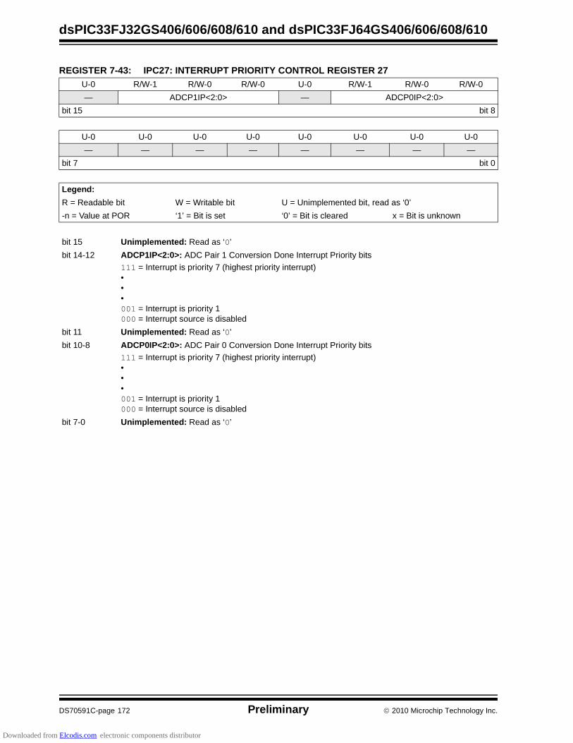
dsPIC33FJ32GS406/606/608/610 and dsPIC33FJ64GS406/606/608/610
DS70591C-page 172 Preliminary 2010 Microchip Technology Inc.
REGISTER 7-43: IPC27: INTERRUPT PRIORITY CONTROL REGISTER 27
U-0 R/W-1 R/W-0 R/W-0 U-0 R/W-1 R/W-0 R/W-0
— ADCP1IP<2:0> — ADCP0IP<2:0>
bit 15 bit 8
U-0 U-0 U-0 U-0 U-0 U-0 U-0 U-0
— — — — — — — —
bit 7 bit 0
Legend:
R = Readable bit W = Writable bit U = Unimplemented bit, read as ‘0’
-n = Value at POR ‘1’ = Bit is set ‘0’ = Bit is cleared x = Bit is unknown
bit 15 Unimplemented: Read as ‘0’
bit 14-12 ADCP1IP<2:0>: ADC Pair 1 Conversion Done Interrupt Priority bits
111 = Interrupt is priority 7 (highest priority interrupt)•••001 = Interrupt is priority 1000 = Interrupt source is disabled
bit 11 Unimplemented: Read as ‘0’
bit 10-8 ADCP0IP<2:0>: ADC Pair 0 Conversion Done Interrupt Priority bits
111 = Interrupt is priority 7 (highest priority interrupt)•••001 = Interrupt is priority 1000 = Interrupt source is disabled
bit 7-0 Unimplemented: Read as ‘0’
Downloaded from Elcodis.com electronic components distributor

2010 Microchip Technology Inc. Preliminary DS70591C-page 173
dsPIC33FJ32GS406/606/608/610 and dsPIC33FJ64GS406/606/608/610
REGISTER 7-44: IPC28: INTERRUPT PRIORITY CONTROL REGISTER 28
U-0 R/W-1 R/W-0 R/W-0 U-0 R/W-1 R/W-0 R/W-0
— ADCP5IP<2:0> — ADCP4IP<2:0>
bit 15 bit 8
U-0 R/W-1 R/W-0 R/W-0 U-0 R/W-1 R/W-0 R/W-0
— ADCP3IP<2:0> — ADCP2IP<2:0>
bit 7 bit 0
Legend:
R = Readable bit W = Writable bit U = Unimplemented bit, read as ‘0’
-n = Value at POR ‘1’ = Bit is set ‘0’ = Bit is cleared x = Bit is unknown
bit 15 Unimplemented: Read as ‘0’
bit 14-12 ADCP5IP<2:0>: ADC Pair 5 Conversion Done Interrupt Priority bits
111 = Interrupt is priority 7 (highest priority interrupt)•••001 = Interrupt is priority 1000 = Interrupt source is disabled
bit 11 Unimplemented: Read as ‘0’
bit 10-8 ADCP4IP<2:0>: ADC Pair 4 Conversion Done Interrupt Priority bits
111 = Interrupt is priority 7 (highest priority interrupt)•••001 = Interrupt is priority 1000 = Interrupt source is disabled
bit 7 Unimplemented: Read as ‘0’
bit 6-4 ADCP3IP<2:0>: ADC Pair 3 Conversion Done Interrupt Priority bits
111 = Interrupt is priority 7 (highest priority interrupt)•••001 = Interrupt is priority 1000 = Interrupt source is disabled
bit 3 Unimplemented: Read as ‘0’
bit 2-0 ADCP2IP<2:0>: ADC Pair 2 Conversion Done Interrupt Priority bits
111 = Interrupt is priority 7 (highest priority interrupt)•••001 = Interrupt is priority 1000 = Interrupt source is disabled
Downloaded from Elcodis.com electronic components distributor
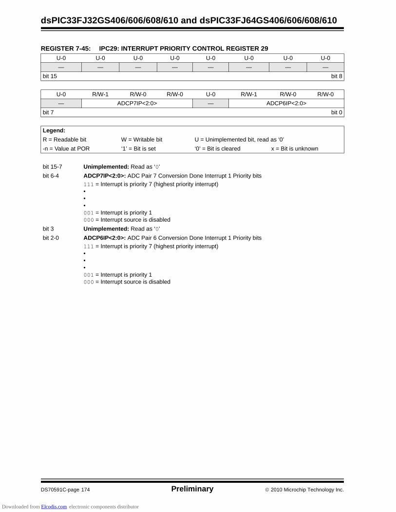
dsPIC33FJ32GS406/606/608/610 and dsPIC33FJ64GS406/606/608/610
DS70591C-page 174 Preliminary 2010 Microchip Technology Inc.
REGISTER 7-45: IPC29: INTERRUPT PRIORITY CONTROL REGISTER 29
U-0 U-0 U-0 U-0 U-0 U-0 U-0 U-0
— — — — — — — —
bit 15 bit 8
U-0 R/W-1 R/W-0 R/W-0 U-0 R/W-1 R/W-0 R/W-0
— ADCP7IP<2:0> — ADCP6IP<2:0>
bit 7 bit 0
Legend:
R = Readable bit W = Writable bit U = Unimplemented bit, read as ‘0’
-n = Value at POR ‘1’ = Bit is set ‘0’ = Bit is cleared x = Bit is unknown
bit 15-7 Unimplemented: Read as ‘0’
bit 6-4 ADCP7IP<2:0>: ADC Pair 7 Conversion Done Interrupt 1 Priority bits
111 = Interrupt is priority 7 (highest priority interrupt)•••001 = Interrupt is priority 1000 = Interrupt source is disabled
bit 3 Unimplemented: Read as ‘0’
bit 2-0 ADCP6IP<2:0>: ADC Pair 6 Conversion Done Interrupt 1 Priority bits
111 = Interrupt is priority 7 (highest priority interrupt)•••001 = Interrupt is priority 1000 = Interrupt source is disabled
Downloaded from Elcodis.com electronic components distributor
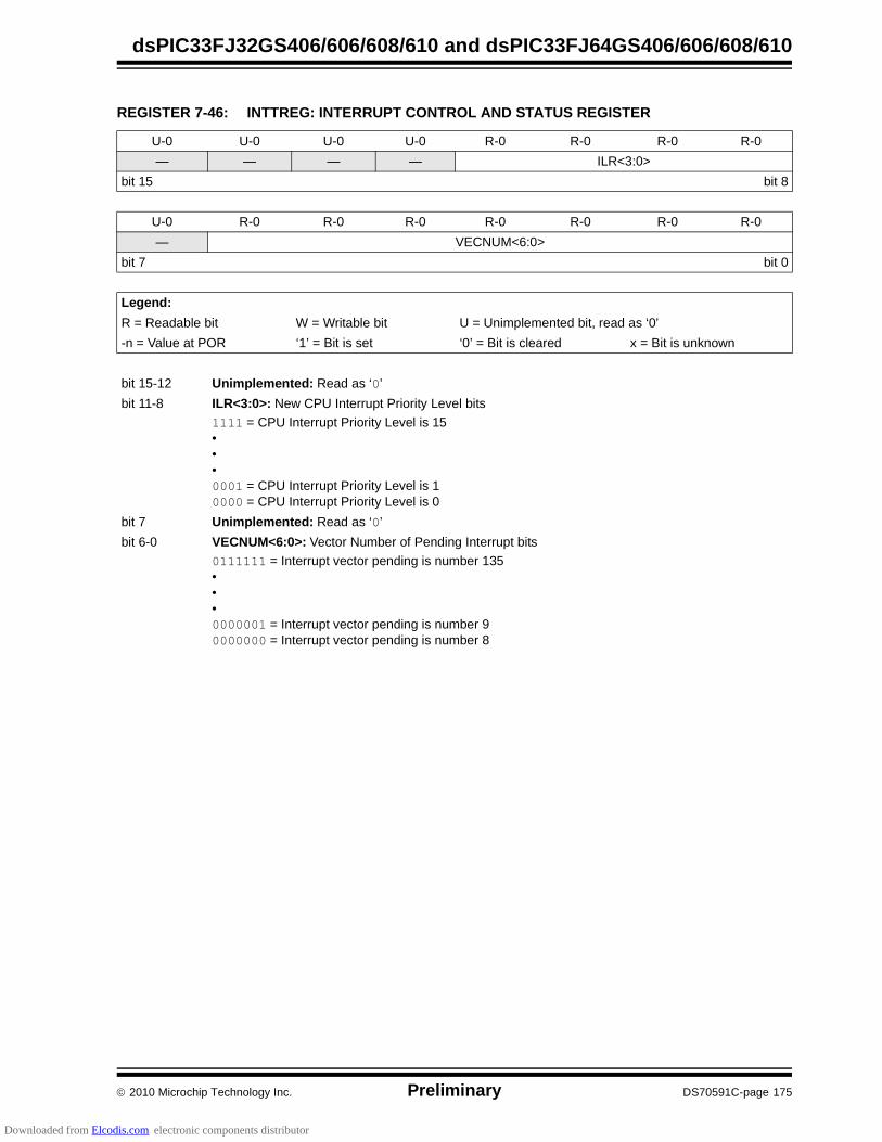
2010 Microchip Technology Inc. Preliminary DS70591C-page 175
dsPIC33FJ32GS406/606/608/610 and dsPIC33FJ64GS406/606/608/610
REGISTER 7-46: INTTREG: INTERRUPT CONTROL AND STATUS REGISTER
U-0 U-0 U-0 U-0 R-0 R-0 R-0 R-0
— — — — ILR<3:0>
bit 15 bit 8
U-0 R-0 R-0 R-0 R-0 R-0 R-0 R-0
— VECNUM<6:0>
bit 7 bit 0
Legend:
R = Readable bit W = Writable bit U = Unimplemented bit, read as ‘0’
-n = Value at POR ‘1’ = Bit is set ‘0’ = Bit is cleared x = Bit is unknown
bit 15-12 Unimplemented: Read as ‘0’
bit 11-8 ILR<3:0>: New CPU Interrupt Priority Level bits
1111 = CPU Interrupt Priority Level is 15 •••0001 = CPU Interrupt Priority Level is 10000 = CPU Interrupt Priority Level is 0
bit 7 Unimplemented: Read as ‘0’
bit 6-0 VECNUM<6:0>: Vector Number of Pending Interrupt bits
0111111 = Interrupt vector pending is number 135 •••0000001 = Interrupt vector pending is number 90000000 = Interrupt vector pending is number 8
Downloaded from Elcodis.com electronic components distributor

dsPIC33FJ32GS406/606/608/610 and dsPIC33FJ64GS406/606/608/610
DS70591C-page 176 Preliminary 2010 Microchip Technology Inc.
7.4 Interrupt Setup Procedures
7.4.1 INITIALIZATION
Complete the following steps to configure an interruptsource at initialization:
1. Set the NSTDIS bit (INTCON1<15>) if nestedinterrupts are not desired.
2. Select the user-assigned priority level for theinterrupt source by writing the control bits in theappropriate IPCx register. The priority level willdepend on the specific application and type ofinterrupt source. If multiple priority levels are notdesired, the IPCx register control bits for allenabled interrupt sources can be programmedto the same non-zero value.
3. Clear the interrupt flag status bit associated withthe peripheral in the associated IFSx register.
4. Enable the interrupt source by setting theinterrupt enable control bit associated with thesource in the appropriate IECx register.
7.4.2 INTERRUPT SERVICE ROUTINE
The method used to declare an ISR and initialize theIVT with the correct vector address depends on theprogramming language (C or assembler) and thelanguage development toolsuite used to develop theapplication.
In general, the user application must clear the interruptflag in the appropriate IFSx register for the source ofinterrupt that the ISR handles. Otherwise, program willre-enter the ISR immediately after exiting the routine. Ifthe ISR is coded in assembly language, it must beterminated using a RETFIE instruction to unstack thesaved PC value, SRL value and old CPU priority level.
7.4.3 TRAP SERVICE ROUTINE
A Trap Service Routine (TSR) is coded like an ISR,except that the appropriate trap status flag in theINTCON1 register must be cleared to avoid re-entryinto the TSR.
7.4.4 INTERRUPT DISABLE
The following steps outline the procedure to disable alluser interrupts:
1. Push the current SR value onto the softwarestack using the PUSH instruction.
2. Force the CPU to priority level 7 by inclusiveORing the value EOh with SRL.
To enable user interrupts, the POP instruction can beused to restore the previous SR value.
The DISI instruction provides a convenient way todisable interrupts of priority levels 1-6 for a fixed periodof time. Level 7 interrupt sources are not disabled bythe DISI instruction.
Note: At a device Reset, the IPCx registers areinitialized such that all user interruptsources are assigned to priority level 4.
Note: Only user interrupts with a priority level of7 or lower can be disabled. Trap sources(level 8-level 15) cannot be disabled.
Downloaded from Elcodis.com electronic components distributor
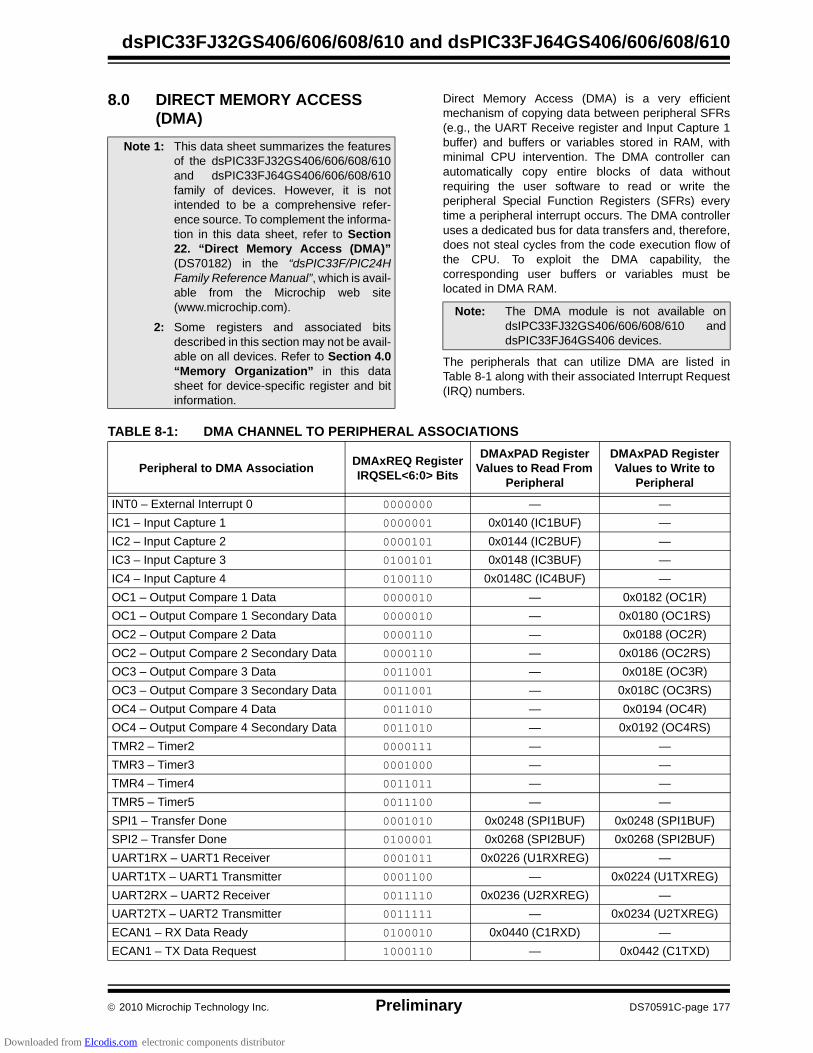
2010 Microchip Technology Inc. Preliminary DS70591C-page 177
dsPIC33FJ32GS406/606/608/610 and dsPIC33FJ64GS406/606/608/610
8.0 DIRECT MEMORY ACCESS (DMA)
Direct Memory Access (DMA) is a very efficientmechanism of copying data between peripheral SFRs(e.g., the UART Receive register and Input Capture 1buffer) and buffers or variables stored in RAM, withminimal CPU intervention. The DMA controller canautomatically copy entire blocks of data withoutrequiring the user software to read or write theperipheral Special Function Registers (SFRs) everytime a peripheral interrupt occurs. The DMA controlleruses a dedicated bus for data transfers and, therefore,does not steal cycles from the code execution flow ofthe CPU. To exploit the DMA capability, thecorresponding user buffers or variables must belocated in DMA RAM.
The peripherals that can utilize DMA are listed inTable 8-1 along with their associated Interrupt Request(IRQ) numbers.
TABLE 8-1: DMA CHANNEL TO PERIPHERAL ASSOCIATIONS
Note 1: This data sheet summarizes the featuresof the dsPIC33FJ32GS406/606/608/610and dsPIC33FJ64GS406/606/608/610family of devices. However, it is notintended to be a comprehensive refer-ence source. To complement the informa-tion in this data sheet, refer to Section22. “Direct Memory Access (DMA)”(DS70182) in the “dsPIC33F/PIC24HFamily Reference Manual”, which is avail-able from the Microchip web site(www.microchip.com).
2: Some registers and associated bitsdescribed in this section may not be avail-able on all devices. Refer to Section 4.0“Memory Organization” in this datasheet for device-specific register and bitinformation.
Note: The DMA module is not available ondsIPC33FJ32GS406/606/608/610 anddsPIC33FJ64GS406 devices.
Peripheral to DMA AssociationDMAxREQ RegisterIRQSEL<6:0> Bits
DMAxPAD Register Values to Read From
Peripheral
DMAxPAD Register Values to Write to
Peripheral
INT0 – External Interrupt 0 0000000 — —
IC1 – Input Capture 1 0000001 0x0140 (IC1BUF) —
IC2 – Input Capture 2 0000101 0x0144 (IC2BUF) —
IC3 – Input Capture 3 0100101 0x0148 (IC3BUF) —
IC4 – Input Capture 4 0100110 0x0148C (IC4BUF) —
OC1 – Output Compare 1 Data 0000010 — 0x0182 (OC1R)
OC1 – Output Compare 1 Secondary Data 0000010 — 0x0180 (OC1RS)
OC2 – Output Compare 2 Data 0000110 — 0x0188 (OC2R)
OC2 – Output Compare 2 Secondary Data 0000110 — 0x0186 (OC2RS)
OC3 – Output Compare 3 Data 0011001 — 0x018E (OC3R)
OC3 – Output Compare 3 Secondary Data 0011001 — 0x018C (OC3RS)
OC4 – Output Compare 4 Data 0011010 — 0x0194 (OC4R)
OC4 – Output Compare 4 Secondary Data 0011010 — 0x0192 (OC4RS)
TMR2 – Timer2 0000111 — —
TMR3 – Timer3 0001000 — —
TMR4 – Timer4 0011011 — —
TMR5 – Timer5 0011100 — —
SPI1 – Transfer Done 0001010 0x0248 (SPI1BUF) 0x0248 (SPI1BUF)
SPI2 – Transfer Done 0100001 0x0268 (SPI2BUF) 0x0268 (SPI2BUF)
UART1RX – UART1 Receiver 0001011 0x0226 (U1RXREG) —
UART1TX – UART1 Transmitter 0001100 — 0x0224 (U1TXREG)
UART2RX – UART2 Receiver 0011110 0x0236 (U2RXREG) —
UART2TX – UART2 Transmitter 0011111 — 0x0234 (U2TXREG)
ECAN1 – RX Data Ready 0100010 0x0440 (C1RXD) —
ECAN1 – TX Data Request 1000110 — 0x0442 (C1TXD)
Downloaded from Elcodis.com electronic components distributor
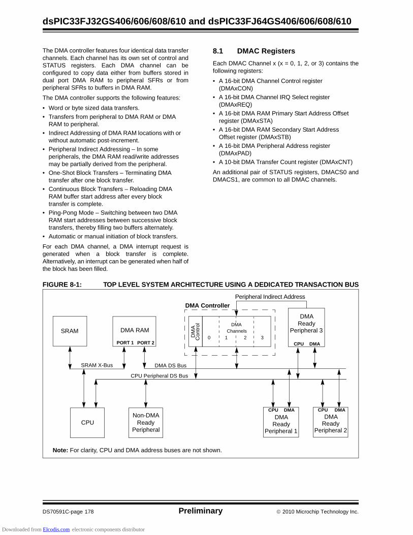
dsPIC33FJ32GS406/606/608/610 and dsPIC33FJ64GS406/606/608/610
DS70591C-page 178 Preliminary 2010 Microchip Technology Inc.
The DMA controller features four identical data transferchannels. Each channel has its own set of control andSTATUS registers. Each DMA channel can beconfigured to copy data either from buffers stored indual port DMA RAM to peripheral SFRs or fromperipheral SFRs to buffers in DMA RAM.
The DMA controller supports the following features:
• Word or byte sized data transfers.
• Transfers from peripheral to DMA RAM or DMA RAM to peripheral.
• Indirect Addressing of DMA RAM locations with or without automatic post-increment.
• Peripheral Indirect Addressing – In some peripherals, the DMA RAM read/write addresses may be partially derived from the peripheral.
• One-Shot Block Transfers – Terminating DMA transfer after one block transfer.
• Continuous Block Transfers – Reloading DMA RAM buffer start address after every block transfer is complete.
• Ping-Pong Mode – Switching between two DMA RAM start addresses between successive block transfers, thereby filling two buffers alternately.
• Automatic or manual initiation of block transfers.
For each DMA channel, a DMA interrupt request isgenerated when a block transfer is complete.Alternatively, an interrupt can be generated when half ofthe block has been filled.
8.1 DMAC Registers
Each DMAC Channel x (x = 0, 1, 2, or 3) contains thefollowing registers:
• A 16-bit DMA Channel Control register (DMAxCON)
• A 16-bit DMA Channel IRQ Select register (DMAxREQ)
• A 16-bit DMA RAM Primary Start Address Offset register (DMAxSTA)
• A 16-bit DMA RAM Secondary Start Address Offset register (DMAxSTB)
• A 16-bit DMA Peripheral Address register (DMAxPAD)
• A 10-bit DMA Transfer Count register (DMAxCNT)
An additional pair of STATUS registers, DMACS0 andDMACS1, are common to all DMAC channels.
FIGURE 8-1: TOP LEVEL SYSTEM ARCHITECTURE USING A DEDICATED TRANSACTION BUS
CPU
SRAM DMA RAM
CPU Peripheral DS Bus
Peripheral 3
DMA
Peripheral
Non-DMA
SRAM X-Bus
PORT 2PORT 1
Peripheral 1
DMAReady
Peripheral 2
DMAReadyReady
Ready
DMA DS Bus
CPU DMA
CPU DMA CPU DMA
Peripheral Indirect Address
Note: For clarity, CPU and DMA address buses are not shown.
DM
AC
on
tro
l
DMA Controller
DMAChannels
0 1 2 3
Downloaded from Elcodis.com electronic components distributor
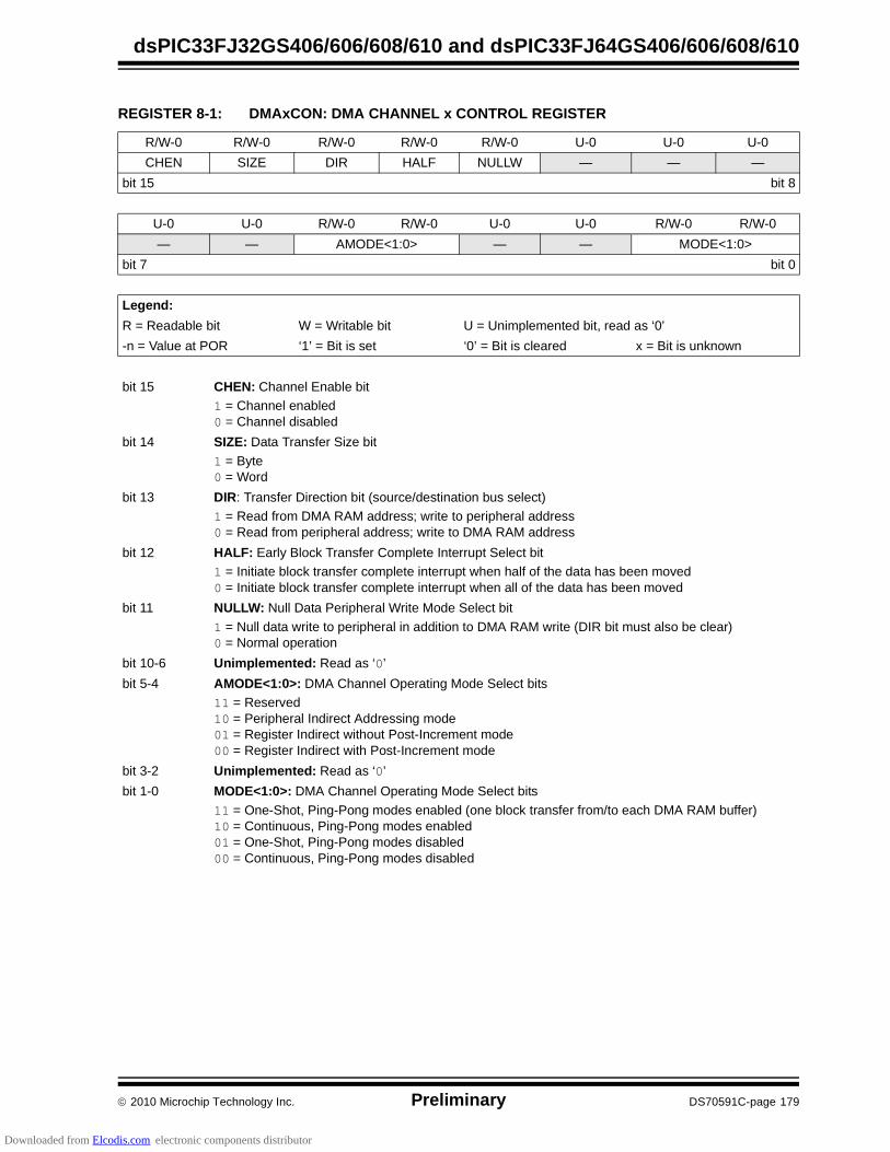
2010 Microchip Technology Inc. Preliminary DS70591C-page 179
dsPIC33FJ32GS406/606/608/610 and dsPIC33FJ64GS406/606/608/610
REGISTER 8-1: DMAxCON: DMA CHANNEL x CONTROL REGISTER
R/W-0 R/W-0 R/W-0 R/W-0 R/W-0 U-0 U-0 U-0
CHEN SIZE DIR HALF NULLW — — —
bit 15 bit 8
U-0 U-0 R/W-0 R/W-0 U-0 U-0 R/W-0 R/W-0
— — AMODE<1:0> — — MODE<1:0>
bit 7 bit 0
Legend:
R = Readable bit W = Writable bit U = Unimplemented bit, read as ‘0’
-n = Value at POR ‘1’ = Bit is set ‘0’ = Bit is cleared x = Bit is unknown
bit 15 CHEN: Channel Enable bit
1 = Channel enabled0 = Channel disabled
bit 14 SIZE: Data Transfer Size bit
1 = Byte0 = Word
bit 13 DIR: Transfer Direction bit (source/destination bus select)
1 = Read from DMA RAM address; write to peripheral address0 = Read from peripheral address; write to DMA RAM address
bit 12 HALF: Early Block Transfer Complete Interrupt Select bit
1 = Initiate block transfer complete interrupt when half of the data has been moved0 = Initiate block transfer complete interrupt when all of the data has been moved
bit 11 NULLW: Null Data Peripheral Write Mode Select bit
1 = Null data write to peripheral in addition to DMA RAM write (DIR bit must also be clear) 0 = Normal operation
bit 10-6 Unimplemented: Read as ‘0’
bit 5-4 AMODE<1:0>: DMA Channel Operating Mode Select bits
11 = Reserved10 = Peripheral Indirect Addressing mode01 = Register Indirect without Post-Increment mode00 = Register Indirect with Post-Increment mode
bit 3-2 Unimplemented: Read as ‘0’
bit 1-0 MODE<1:0>: DMA Channel Operating Mode Select bits
11 = One-Shot, Ping-Pong modes enabled (one block transfer from/to each DMA RAM buffer)10 = Continuous, Ping-Pong modes enabled01 = One-Shot, Ping-Pong modes disabled00 = Continuous, Ping-Pong modes disabled
Downloaded from Elcodis.com electronic components distributor

dsPIC33FJ32GS406/606/608/610 and dsPIC33FJ64GS406/606/608/610
DS70591C-page 180 Preliminary 2010 Microchip Technology Inc.
REGISTER 8-2: DMAxREQ: DMA CHANNEL x IRQ SELECT REGISTER
R/W-0 U-0 U-0 U-0 U-0 U-0 U-0 U-0
FORCE(1) — — — — — — —
bit 15 bit 8
U-0 R/W-1 R/W-1 R/W-1 R/W-1 R/W-1 R/W-1 R/W-1
— IRQSEL<6:0>(2)
bit 7 bit 0
Legend:
R = Readable bit W = Writable bit U = Unimplemented bit, read as ‘0’
-n = Value at POR ‘1’ = Bit is set ‘0’ = Bit is cleared x = Bit is unknown
bit 15 FORCE: Force DMA Transfer bit(1)
1 = Force a single DMA transfer (Manual mode)0 = Automatic DMA transfer initiation by DMA request
bit 14-7 Unimplemented: Read as ‘0’
bit 6-0 IRQSEL<6:0>: DMA Peripheral IRQ Number Select bits(2)
0000000-1111111 = DMAIRQ0-DMAIRQ127 selected to be Channel DMAREQ
Note 1: The FORCE bit cannot be cleared by the user. The FORCE bit is cleared by hardware when the forcedDMA transfer is complete.
2: See Table 8-1 for a complete listing of IRQ numbers for all interrupt sources.
Downloaded from Elcodis.com electronic components distributor
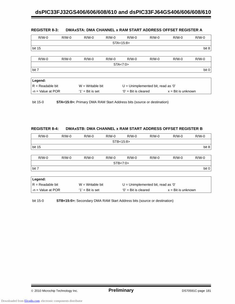
2010 Microchip Technology Inc. Preliminary DS70591C-page 181
dsPIC33FJ32GS406/606/608/610 and dsPIC33FJ64GS406/606/608/610
REGISTER 8-3: DMAxSTA: DMA CHANNEL x RAM START ADDRESS OFFSET REGISTER A
R/W-0 R/W-0 R/W-0 R/W-0 R/W-0 R/W-0 R/W-0 R/W-0
STA<15:8>
bit 15 bit 8
R/W-0 R/W-0 R/W-0 R/W-0 R/W-0 R/W-0 R/W-0 R/W-0
STA<7:0>
bit 7 bit 0
Legend:
R = Readable bit W = Writable bit U = Unimplemented bit, read as ‘0’
-n = Value at POR ‘1’ = Bit is set ‘0’ = Bit is cleared x = Bit is unknown
bit 15-0 STA<15:0>: Primary DMA RAM Start Address bits (source or destination)
REGISTER 8-4: DMAxSTB: DMA CHANNEL x RAM START ADDRESS OFFSET REGISTER B
R/W-0 R/W-0 R/W-0 R/W-0 R/W-0 R/W-0 R/W-0 R/W-0
STB<15:8>
bit 15 bit 8
R/W-0 R/W-0 R/W-0 R/W-0 R/W-0 R/W-0 R/W-0 R/W-0
STB<7:0>
bit 7 bit 0
Legend:
R = Readable bit W = Writable bit U = Unimplemented bit, read as ‘0’
-n = Value at POR ‘1’ = Bit is set ‘0’ = Bit is cleared x = Bit is unknown
bit 15-0 STB<15:0>: Secondary DMA RAM Start Address bits (source or destination)
Downloaded from Elcodis.com electronic components distributor
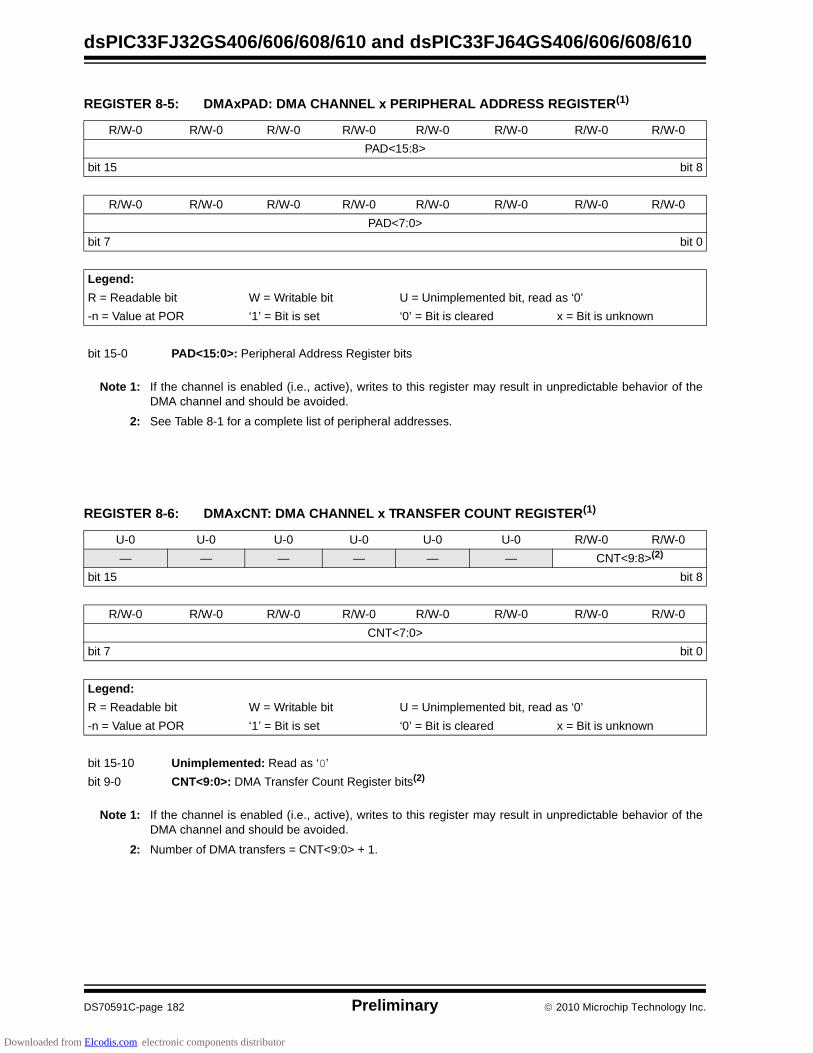
dsPIC33FJ32GS406/606/608/610 and dsPIC33FJ64GS406/606/608/610
DS70591C-page 182 Preliminary 2010 Microchip Technology Inc.
REGISTER 8-5: DMAxPAD: DMA CHANNEL x PERIPHERAL ADDRESS REGISTER(1)
R/W-0 R/W-0 R/W-0 R/W-0 R/W-0 R/W-0 R/W-0 R/W-0
PAD<15:8>
bit 15 bit 8
R/W-0 R/W-0 R/W-0 R/W-0 R/W-0 R/W-0 R/W-0 R/W-0
PAD<7:0>
bit 7 bit 0
Legend:
R = Readable bit W = Writable bit U = Unimplemented bit, read as ‘0’
-n = Value at POR ‘1’ = Bit is set ‘0’ = Bit is cleared x = Bit is unknown
bit 15-0 PAD<15:0>: Peripheral Address Register bits
Note 1: If the channel is enabled (i.e., active), writes to this register may result in unpredictable behavior of theDMA channel and should be avoided.
2: See Table 8-1 for a complete list of peripheral addresses.
REGISTER 8-6: DMAxCNT: DMA CHANNEL x TRANSFER COUNT REGISTER(1)
U-0 U-0 U-0 U-0 U-0 U-0 R/W-0 R/W-0
— — — — — — CNT<9:8>(2)
bit 15 bit 8
R/W-0 R/W-0 R/W-0 R/W-0 R/W-0 R/W-0 R/W-0 R/W-0
CNT<7:0>
bit 7 bit 0
Legend:
R = Readable bit W = Writable bit U = Unimplemented bit, read as ‘0’
-n = Value at POR ‘1’ = Bit is set ‘0’ = Bit is cleared x = Bit is unknown
bit 15-10 Unimplemented: Read as ‘0’
bit 9-0 CNT<9:0>: DMA Transfer Count Register bits(2)
Note 1: If the channel is enabled (i.e., active), writes to this register may result in unpredictable behavior of theDMA channel and should be avoided.
2: Number of DMA transfers = CNT<9:0> + 1.
Downloaded from Elcodis.com electronic components distributor

2010 Microchip Technology Inc. Preliminary DS70591C-page 183
dsPIC33FJ32GS406/606/608/610 and dsPIC33FJ64GS406/606/608/610
REGISTER 8-7: DMACS0: DMA CONTROLLER STATUS REGISTER 0
U-0 U-0 U-0 U-0 R/C-0 R/C-0 R/C-0 R/C-0
— — — — PWCOL3 PWCOL2 PWCOL1 PWCOL0
bit 15 bit 8
U-0 U-0 U-0 U-0 R/C-0 R/C-0 R/C-0 R/C-0
— — — — XWCOL3 XWCOL2 XWCOL1 XWCOL0
bit 7 bit 0
Legend:
R = Readable bit W = Writable bit U = Unimplemented bit, read as ‘0’
-n = Value at POR ‘1’ = Bit is set ‘0’ = Bit is cleared x = Bit is unknown
bit 15-12 Unimplemented: Read as ‘0’
bit 11 PWCOL3: Channel 3 Peripheral Write Collision Flag bit
1 = Write collision detected0 = No write collision detected
bit 10 PWCOL2: Channel 2 Peripheral Write Collision Flag bit
1 = Write collision detected0 = No write collision detected
bit 9 PWCOL1: Channel 1 Peripheral Write Collision Flag bit
1 = Write collision detected0 = No write collision detected
bit 8 PWCOL0: Channel 0 Peripheral Write Collision Flag bit
1 = Write collision detected0 = No write collision detected
bit 7-4 Unimplemented: Read as ‘0’
bit 3 XWCOL3: Channel 3 DMA RAM Write Collision Flag bit
1 = Write collision detected0 = No write collision detected
bit 2 XWCOL2: Channel 2 DMA RAM Write Collision Flag bit
1 = Write collision detected0 = No write collision detected
bit 1 XWCOL1: Channel 1 DMA RAM Write Collision Flag bit
1 = Write collision detected0 = No write collision detected
bit 0 XWCOL0: Channel 0 DMA RAM Write Collision Flag bit
1 = Write collision detected0 = No write collision detected
Downloaded from Elcodis.com electronic components distributor

dsPIC33FJ32GS406/606/608/610 and dsPIC33FJ64GS406/606/608/610
DS70591C-page 184 Preliminary 2010 Microchip Technology Inc.
REGISTER 8-8: DMACS1: DMA CONTROLLER STATUS REGISTER 1
U-0 U-0 U-0 U-0 R-1 R-1 R-1 R-1
— — — — LSTCH<3:0>
bit 15 bit 8
U-0 U-0 U-0 U-0 R-0 R-0 R-0 R-0
— — — — PPST3 PPST2 PPST1 PPST0
bit 7 bit 0
Legend:
R = Readable bit W = Writable bit U = Unimplemented bit, read as ‘0’
-n = Value at POR ‘1’ = Bit is set ‘0’ = Bit is cleared x = Bit is unknown
bit 15-12 Unimplemented: Read as ‘0’
bit 11-8 LSTCH<3:0>: Last DMA Channel Active bits
1111 = No DMA transfer has occurred since system Reset1110-0100 = Reserved0011 = Last data transfer was by DMA Channel 30010 = Last data transfer was by DMA Channel 20001 = Last data transfer was by DMA Channel 10000 = Last data transfer was by DMA Channel 0
bit 7-4 Unimplemented: Read as ‘0’
bit 3 PPST3: Channel 3 Ping-Pong Mode Status Flag bit
1 = DMA3STB register selected0 = DMA3STA register selected
bit 2 PPST2: Channel 2 Ping-Pong Mode Status Flag bit
1 = DMA2STB register selected0 = DMA2STA register selected
bit 1 PPST1: Channel 1 Ping-Pong Mode Status Flag bit
1 = DMA1STB register selected0 = DMA1STA register selected
bit 0 PPST0: Channel 0 Ping-Pong Mode Status Flag bit
1 = DMA0STB register selected0 = DMA0STA register selected
Downloaded from Elcodis.com electronic components distributor

2010 Microchip Technology Inc. Preliminary DS70591C-page 185
dsPIC33FJ32GS406/606/608/610 and dsPIC33FJ64GS406/606/608/610
REGISTER 8-9: DSADR: MOST RECENT DMA RAM ADDRESS
R-0 R-0 R-0 R-0 R-0 R-0 R-0 R-0
DSADR<15:8>
bit 15 bit 8
R-0 R-0 R-0 R-0 R-0 R-0 R-0 R-0
DSADR<7:0>
bit 7 bit 0
Legend:
R = Readable bit W = Writable bit U = Unimplemented bit, read as ‘0’
-n = Value at POR ‘1’ = Bit is set ‘0’ = Bit is cleared x = Bit is unknown
bit 15-0 DSADR<15:0>: Most Recent DMA RAM Address Accessed by DMA Controller bits
Downloaded from Elcodis.com electronic components distributor

dsPIC33FJ32GS406/606/608/610 and dsPIC33FJ64GS406/606/608/610
DS70591C-page 186 Preliminary 2010 Microchip Technology Inc.
NOTES:
Downloaded from Elcodis.com electronic components distributor

2010 Microchip Technology Inc. Preliminary DS70591C-page 187
dsPIC33FJ32GS406/606/608/610 and dsPIC33FJ64GS406/606/608/610
9.0 OSCILLATOR CONFIGURATION
The dsPIC33FJ32GS406/606/608/610 anddsPIC33FJ64GS406/606/608/610 oscillator systemprovides:
• External and internal oscillator options as clock sources
• An on-chip Phase-Locked Loop (PLL) to scale the internal operating frequency to the required system clock frequency
• An internal FRC oscillator that can also be used with the PLL, thereby allowing full-speed operation without any external clock generation hardware
• Clock switching between various clock sources
• Programmable clock postscaler for system power savings
• A Fail-Safe Clock Monitor (FSCM) that detects clock failure and takes fail-safe measures
• A Clock Control register (OSCCON)
• Nonvolatile Configuration bits for main oscillator selection.
• Auxiliary PLL for ADC and PWM
A simplified diagram of the oscillator system is shownin Figure 9-1.
Note 1: This data sheet summarizes the featuresof the dsPIC33FJ32GS406/606/608/610and dsPIC33FJ64GS406/606/608/610families of devices. It is not intended to bea comprehensive reference source. Tocomplement the information in this datasheet, refer to Section 42. “Oscillator(Part IV)” (DS70307) in the “dsPIC33FFamily Reference Manual”, which isavailable from the Microchip web site(www.microchip.com).
2: Some registers and associated bitsdescribed in this section may not be avail-able on all devices. Refer to Section 4.0“Memory Organization” in this datasheet for device-specific register and bitinformation.
Downloaded from Elcodis.com electronic components distributor

dsPIC33FJ32GS406/606/608/610 and dsPIC33FJ64GS406/606/608/610
DS70591C-page 188 Preliminary 2010 Microchip Technology Inc.
FIGURE 9-1: dsPIC33FJ32GS406/606/608/610 and dsPIC33FJ64GS406/606/608/610 OSCILLATOR SYSTEM DIAGRAM
÷ N
ACLK
SELACLK APSTSCLR<2:0>
To PWM/ADC
ENAPLL
APLLx16
ASRCSEL FRCSEL
POSCCLKFRCCLK
÷ N
ROSEL RODIV<3:0>
REFCLKO(3)
POSCCLK
Reference Clock Generation
Auxiliary Clock Generation
Note 1: See Figure 9-2 for PLL details.
2: If the Oscillator is used with XT or HS modes, an external parallel resistor with the value of 1 M must be connected.
3: REFCLKO functionality is not available if the Primary Oscillator is used.
FVCO(1)
FOSC
Secondary Oscillator (SOSC)
LPOSCEN
SOSCO
SOSCI
Timer 1
OSC2
OSC1Primary Oscillator (POSC)
XTPLL, HSPLL,
XT, HS, EC
FRCDIV<2:0>
WDT, PWRT, FSCM
FRCDIVN
SOSC
FRCDIV16
ECPLL, FRCPLL
NOSC<2:0> FNOSC<2:0>
Reset
FRCOscillator
LPRCOscillator
DOZE<2:0>
S3
S1
S2
S1/S3
S7
S6
FRC
LPRC
S0
S5
S4
÷ 16
Clock Switch
S7
Clock Fail
÷ 2
TUN<5:0>
PLL(1) FCY
FOSCF
RC
DIV
DO
ZE
FVCO(1)
To ADC andAuxiliary ClockGenerator
R(2)
POSCMD<1:0>
POSCCLK
FP
Downloaded from Elcodis.com electronic components distributor
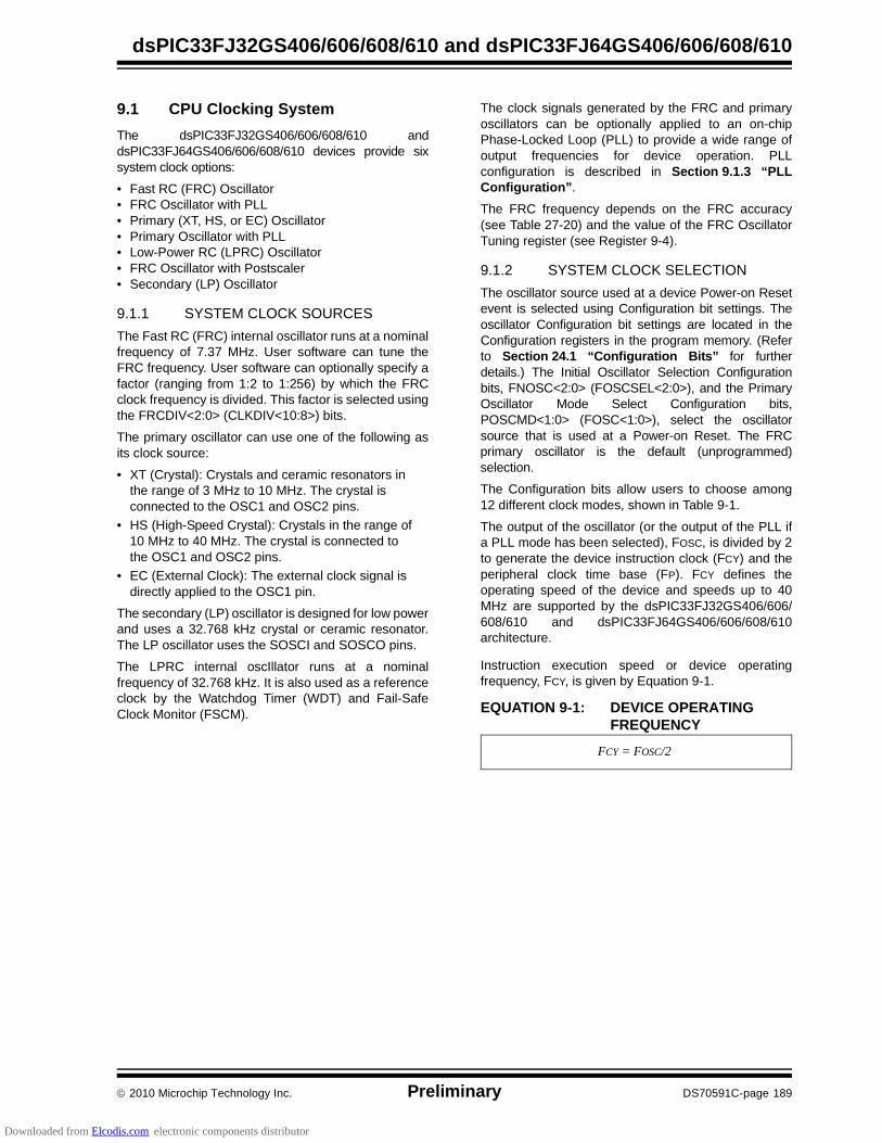
2010 Microchip Technology Inc. Preliminary DS70591C-page 189
dsPIC33FJ32GS406/606/608/610 and dsPIC33FJ64GS406/606/608/610
9.1 CPU Clocking System
The dsPIC33FJ32GS406/606/608/610 anddsPIC33FJ64GS406/606/608/610 devices provide sixsystem clock options:
• Fast RC (FRC) Oscillator• FRC Oscillator with PLL• Primary (XT, HS, or EC) Oscillator• Primary Oscillator with PLL• Low-Power RC (LPRC) Oscillator• FRC Oscillator with Postscaler• Secondary (LP) Oscillator
9.1.1 SYSTEM CLOCK SOURCES
The Fast RC (FRC) internal oscillator runs at a nominalfrequency of 7.37 MHz. User software can tune theFRC frequency. User software can optionally specify afactor (ranging from 1:2 to 1:256) by which the FRCclock frequency is divided. This factor is selected usingthe FRCDIV<2:0> (CLKDIV<10:8>) bits.
The primary oscillator can use one of the following asits clock source:
• XT (Crystal): Crystals and ceramic resonators in the range of 3 MHz to 10 MHz. The crystal is connected to the OSC1 and OSC2 pins.
• HS (High-Speed Crystal): Crystals in the range of 10 MHz to 40 MHz. The crystal is connected to the OSC1 and OSC2 pins.
• EC (External Clock): The external clock signal is directly applied to the OSC1 pin.
The secondary (LP) oscillator is designed for low powerand uses a 32.768 kHz crystal or ceramic resonator.The LP oscillator uses the SOSCI and SOSCO pins.
The LPRC internal oscIllator runs at a nominalfrequency of 32.768 kHz. It is also used as a referenceclock by the Watchdog Timer (WDT) and Fail-SafeClock Monitor (FSCM).
The clock signals generated by the FRC and primaryoscillators can be optionally applied to an on-chipPhase-Locked Loop (PLL) to provide a wide range ofoutput frequencies for device operation. PLLconfiguration is described in Section 9.1.3 “PLLConfiguration”.
The FRC frequency depends on the FRC accuracy(see Table 27-20) and the value of the FRC OscillatorTuning register (see Register 9-4).
9.1.2 SYSTEM CLOCK SELECTION
The oscillator source used at a device Power-on Resetevent is selected using Configuration bit settings. Theoscillator Configuration bit settings are located in theConfiguration registers in the program memory. (Referto Section 24.1 “Configuration Bits” for furtherdetails.) The Initial Oscillator Selection Configurationbits, FNOSC<2:0> (FOSCSEL<2:0>), and the PrimaryOscillator Mode Select Configuration bits,POSCMD<1:0> (FOSC<1:0>), select the oscillatorsource that is used at a Power-on Reset. The FRCprimary oscillator is the default (unprogrammed)selection.
The Configuration bits allow users to choose among12 different clock modes, shown in Table 9-1.
The output of the oscillator (or the output of the PLL ifa PLL mode has been selected), FOSC, is divided by 2to generate the device instruction clock (FCY) and theperipheral clock time base (FP). FCY defines theoperating speed of the device and speeds up to 40MHz are supported by the dsPIC33FJ32GS406/606/608/610 and dsPIC33FJ64GS406/606/608/610architecture.
Instruction execution speed or device operatingfrequency, FCY, is given by Equation 9-1.
EQUATION 9-1: DEVICE OPERATING FREQUENCY
FCY = FOSC/2
Downloaded from Elcodis.com electronic components distributor
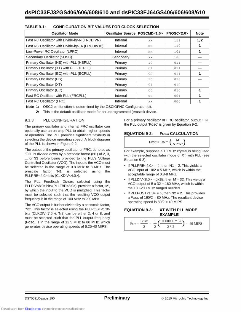
dsPIC33FJ32GS406/606/608/610 and dsPIC33FJ64GS406/606/608/610
DS70591C-page 190 Preliminary 2010 Microchip Technology Inc.
TABLE 9-1: CONFIGURATION BIT VALUES FOR CLOCK SELECTION
9.1.3 PLL CONFIGURATION
The primary oscillator and internal FRC oscillator canoptionally use an on-chip PLL to obtain higher speedsof operation. The PLL provides significant flexibility inselecting the device operating speed. A block diagramof the PLL is shown in Figure 9-2.
The output of the primary oscillator or FRC, denoted as‘FIN’, is divided down by a prescale factor (N1) of 2, 3,... or 33 before being provided to the PLL’s VoltageControlled Oscillator (VCO). The input to the VCO mustbe selected in the range of 0.8 MHz to 8 MHz. Theprescale factor ‘N1’ is selected using thePLLPRE<4:0> bits (CLKDIV<4:0>).
The PLL Feedback Divisor, selected using thePLLDIV<8:0> bits (PLLFBD<8:0>), provides a factor, ‘M’,by which the input to the VCO is multiplied. This factormust be selected such that the resulting VCO outputfrequency is in the range of 100 MHz to 200 MHz.
The VCO output is further divided by a postscale factor,‘N2’. This factor is selected using the PLLPOST<1:0>bits (CLKDIV<7:6>). ‘N2’ can be either 2, 4 or 8, andmust be selected such that the PLL output frequency(FOSC) is in the range of 12.5 MHz to 80 MHz, whichgenerates device operating speeds of 6.25-40 MIPS.
For a primary oscillator or FRC oscillator, output ‘FIN’,the PLL output ‘FOSC’ is given by Equation 9-2.
EQUATION 9-2: FOSC CALCULATION
For example, suppose a 10 MHz crystal is being usedwith the selected oscillator mode of XT with PLL (seeEquation 9-3).
• If PLLPRE<4:0> = 0, then N1 = 2. This yields a VCO input of 10/2 = 5 MHz, which is within the acceptable range of 0.8-8 MHz.
• If PLLDIV<8:0> = 0x1E, then M = 32. This yields a VCO output of 5 x 32 = 160 MHz, which is within the 100-200 MHz ranged needed.
• If PLLPOST<1:0> = 0, then N2 = 2. This provides a FOSC of 160/2 = 80 MHz. The resultant device operating speed is 80/2 = 40 MIPS.
EQUATION 9-3: XT WITH PLL MODE EXAMPLE
Oscillator Mode Oscillator Source POSCMD<1:0> FNOSC<2:0> Note
Fast RC Oscillator with Divide-by-N (FRCDIVN) Internal xx 111 1, 2
Fast RC Oscillator with Divide-by-16 (FRCDIV16) Internal xx 110 1
Low-Power RC Oscillator (LPRC) Internal xx 101 1
Secondary Oscillator (SOSC) Secondary xx 100 —
Primary Oscillator (HS) with PLL (HSPLL) Primary 10 011 —
Primary Oscillator (XT) with PLL (XTPLL) Primary 01 011 —
Primary Oscillator (EC) with PLL (ECPLL) Primary 00 011 1
Primary Oscillator (HS) Primary 10 010 —
Primary Oscillator (XT) Primary 01 010 —
Primary Oscillator (EC) Primary 00 010 1
Fast RC Oscillator with PLL (FRCPLL) Internal xx 001 1
Fast RC Oscillator (FRC) Internal xx 000 1
Note 1: OSC2 pin function is determined by the OSCIOFNC Configuration bit.
2: This is the default oscillator mode for an unprogrammed (erased) device.
( ) M N1*N2
FOSC = FIN *
FCY = FOSC
2= =
1
2(10000000 * 32
2 * 2) 40 MIPS
Downloaded from Elcodis.com electronic components distributor

2010 Microchip Technology Inc. Preliminary DS70591C-page 191
dsPIC33FJ32GS406/606/608/610 and dsPIC33FJ64GS406/606/608/610
FIGURE 9-2: dsPIC33FJ32GS406/606/608/610 and dsPIC33FJ64GS406/606/608/610 PLL BLOCK DIAGRAM
9.2 Auxiliary Clock Generation
The auxiliary clock generation is used for a peripheralsthat need to operate at a frequency unrelated to thesystem clock such as a PWM or ADC.
The primary oscillator and internal FRC oscillatorsources can be used with an auxiliary PLL to obtain theauxiliary clock. The auxiliary PLL has a fixed 16xmultiplication factor.
9.3 Reference Clock Generation
The reference clock output logic provides the user withthe ability to output a clock signal based on the systemclock or the crystal oscillator on a device pin. The userapplication can specify a wide range of clock scalingprior to outputting the reference clock.
0.8-8.0 MHzHere(1) 100-200 MHz
Here(1)
Divide by2, 4, 8
Divide by2-513
Divide by2-33
Source (Crystal, External ClockPLLPRE X VCO
PLLDIV
PLLPOSTor Internal RC)
12.5-80 MHzHere(1)
FOSC
Note 1: This frequency range must be satisfied at all times.
N1
M
N2
FVCO
Note: To achieve 1.04 ns PWM resolution, theauxiliary clock must be set up for 120 MHz.
Note: If the primary PLL is used as a source forthe auxiliary clock, then the primary PLLshould be configured up to a maximumoperation of 30 MIPS or less.
Downloaded from Elcodis.com electronic components distributor

dsPIC33FJ32GS406/606/608/610 and dsPIC33FJ64GS406/606/608/610
DS70591C-page 192 Preliminary 2010 Microchip Technology Inc.
REGISTER 9-1: OSCCON: OSCILLATOR CONTROL REGISTER(1)
U-0 R-y R-y R-y U-0 R/W-y R/W-y R/W-y
— COSC<2:0> — NOSC<2:0>(2)
bit 15 bit 8
R/W-0 U-0 R-0 U-0 R/C-0 U-0 U-0 R/W-0
CLKLOCK — LOCK — CF — — OSWEN
bit 7 bit 0
Legend: y = Value set from Configuration bits on POR
R = Readable bit W = Writable bit U = Unimplemented bit, read as ‘0’
-n = Value at POR ‘1’ = Bit is set ‘0’ = Bit is cleared x = Bit is unknown
bit 15 Unimplemented: Read as ‘0’
bit 14-12 COSC<2:0>: Current Oscillator Selection bits (read-only)
000 = Fast RC oscillator (FRC)001 = Fast RC oscillator (FRC) with PLL 010 = Primary oscillator (XT, HS, EC)011 = Primary oscillator (XT, HS, EC) with PLL 100 = Secondary oscillator (SOSC)101 = Low-Power RC oscillator (LPRC)110 = Fast RC oscillator (FRC) with divide-by-16111 = Fast RC oscillator (FRC) with divide-by-n
bit 11 Unimplemented: Read as ‘0’
bit 10-8 NOSC<2:0>: New Oscillator Selection bits(2)
000 = Fast RC oscillator (FRC)001 = Fast RC oscillator (FRC) with PLL 010 = Primary oscillator (XT, HS, EC)011 = Primary oscillator (XT, HS, EC) with PLL 100 = Secondary oscillator (SOSC)101 = Low-Power RC oscillator (LPRC)110 = Fast RC oscillator (FRC) with divide-by-16111 = Fast RC oscillator (FRC) with divide-by-n
bit 7 CLKLOCK: Clock Lock Enable bit
If clock switching is enabled and FSCM is disabled, (FOSC<FCKSM> = 0b01):1 = Clock switching is disabled, system clock source is locked0 = Clock switching is enabled, system clock source can be modified by clock switching
bit 6 Unimplemented: Read as ‘0’
bit 5 LOCK: PLL Lock Status bit (read-only)
1 = Indicates that PLL is in lock, or PLL start-up timer is satisfied0 = Indicates that PLL is out of lock, start-up timer is in progress or PLL is disabled
bit 4 Unimplemented: Read as ‘0’
bit 3 CF: Clock Fail Detect bit (read/clear by application)
1 = FSCM has detected clock failure0 = FSCM has not detected clock failure
bit 2-1 Unimplemented: Read as ‘0’
bit 0 OSWEN: Oscillator Switch Enable bit
1 = Request oscillator switch to selection specified by NOSC<2:0> bits0 = Oscillator switch is complete
Note 1: Writes to this register require an unlock sequence. Refer to Section 42. “Oscillator (Part IV)” (DS70307)in the “dsPIC33F Family Reference Manual” (available from the Microchip web site) for details.
2: Direct clock switches between any primary oscillator mode with PLL and FRCPLL mode are not permitted.This applies to clock switches in either direction. In these instances, the application must switch to FRC modeas a transition clock source between the two PLL modes.
Downloaded from Elcodis.com electronic components distributor

2010 Microchip Technology Inc. Preliminary DS70591C-page 193
dsPIC33FJ32GS406/606/608/610 and dsPIC33FJ64GS406/606/608/610
REGISTER 9-2: CLKDIV: CLOCK DIVISOR REGISTER
R/W-0 R/W-0 R/W-1 R/W-1 R/W-0 R/W-0 R/W-0 R/W-0
ROI DOZE<2:0> DOZEN(1) FRCDIV<2:0>
bit 15 bit 8
R/W-0 R/W-1 U-0 R/W-0 R/W-0 R/W-0 R/W-0 R/W-0
PLLPOST<1:0> — PLLPRE<4:0>
bit 7 bit 0
Legend:
R = Readable bit W = Writable bit U = Unimplemented bit, read as ‘0’
-n = Value at POR ‘1’ = Bit is set ‘0’ = Bit is cleared x = Bit is unknown
bit 15 ROI: Recover on Interrupt bit
1 = Interrupts will clear the DOZEN bit and the processor clock/peripheral clock ratio is set to 1:10 = Interrupts have no effect on the DOZEN bit
bit 14-12 DOZE<2:0>: Processor Clock Reduction Select bits
000 = FCY/1001 = FCY/2010 = FCY/4011 = FCY/8 (default)100 = FCY/16101 = FCY/32110 = FCY/64111 = FCY/128
bit 11 DOZEN: Doze Mode Enable bit(1)
1 = DOZE<2:0> field specifies the ratio between the peripheral clocks and the processor clocks0 = Processor clock/peripheral clock ratio forced to 1:1
bit 10-8 FRCDIV<2:0>: Internal Fast RC Oscillator Postscaler bits
000 = FRC divide by 1 (default)001 = FRC divide by 2010 = FRC divide by 4011 = FRC divide by 8100 = FRC divide by 16101 = FRC divide by 32110 = FRC divide by 64111 = FRC divide by 256
bit 7-6 PLLPOST<1:0>: PLL VCO Output Divider Select bits (also denoted as ‘N2’, PLL postscaler)
00 = Output/2 01 = Output/4 (default)10 = Reserved11 = Output/8
bit 5 Unimplemented: Read as ‘0’
bit 4-0 PLLPRE<4:0>: PLL Phase Detector Input Divider bits (also denoted as ‘N1’, PLL prescaler)
00000 = Input/2 (default)00001 = Input/3
•
•
•
11111 = Input/33
Note 1: This bit is cleared when the ROI bit is set and an interrupt occurs.
Downloaded from Elcodis.com electronic components distributor

dsPIC33FJ32GS406/606/608/610 and dsPIC33FJ64GS406/606/608/610
DS70591C-page 194 Preliminary 2010 Microchip Technology Inc.
REGISTER 9-3: PLLFBD: PLL FEEDBACK DIVISOR REGISTER
U-0 U-0 U-0 U-0 U-0 U-0 U-0 R/W-0
— — — — — — — PLLDIV<8>
bit 15 bit 8
R/W-0 R/W-0 R/W-1 R/W-1 R/W-0 R/W-0 R/W-0 R/W-0
PLLDIV<7:0>
bit 7 bit 0
Legend:
R = Readable bit W = Writable bit U = Unimplemented bit, read as ‘0’
-n = Value at POR ‘1’ = Bit is set ‘0’ = Bit is cleared x = Bit is unknown
bit 15-9 Unimplemented: Read as ‘0’
bit 8-0 PLLDIV<8:0>: PLL Feedback Divisor bits (also denoted as ‘M’, PLL multiplier)
000000000 = 2000000001 = 3000000010 = 4
•
•
•
000110000 = 50 (default)
•
•
•
111111111 = 513
Downloaded from Elcodis.com electronic components distributor

2010 Microchip Technology Inc. Preliminary DS70591C-page 195
dsPIC33FJ32GS406/606/608/610 and dsPIC33FJ64GS406/606/608/610
REGISTER 9-4: OSCTUN: OSCILLATOR TUNING REGISTER
U-0 U-0 U-0 U-0 U-0 U-0 U-0 U-0
— — — — — — — —
bit 15 bit 8
U-0 U-0 R/W-0 R/W-0 R/W-0 R/W-0 R/W-0 R/W-0
— — TUN<5:0>(1)
bit 7 bit 0
Legend:
R = Readable bit W = Writable bit U = Unimplemented bit, read as ‘0’
-n = Value at POR ‘1’ = Bit is set ‘0’ = Bit is cleared x = Bit is unknown
bit 15-6 Unimplemented: Read as ‘0’
bit 5-0 TUN<5:0>: FRC Oscillator Tuning bits(1)
011111 = Center frequency + 11.625% (8.23 MHz)011110 = Center frequency + 11.25% (8.20 MHz)
•
•
•
000001 = Center frequency + 0.375% (7.40 MHz) 000000 = Center frequency (7.37 MHz nominal)111111 = Center frequency -0.375% (7.345 MHz)
•
•
•
100001 = Center frequency -11.625% (6.52 MHz) 100000 = Center frequency -12% (6.49 MHz)
Note 1: OSCTUN functionality has been provided to help customers compensate for temperature effects on theFRC frequency over a wide range of temperatures. The tuning step size is an approximation and is neithercharacterized nor tested.
Downloaded from Elcodis.com electronic components distributor

dsPIC33FJ32GS406/606/608/610 and dsPIC33FJ64GS406/606/608/610
DS70591C-page 196 Preliminary 2010 Microchip Technology Inc.
REGISTER 9-5: ACLKCON: AUXILIARY CLOCK DIVISOR CONTROL REGISTER
R/W-0 R-0 R/W-1 U-0 U-0 R/W-1 R/W-1 R/W-1
ENAPLL APLLCK SELACLK — — APSTSCLR<2:0>
bit 15 bit 0
R/W-0 R/W-0 U-0 U-0 U-0 U-0 U-0 U-0
ASRCSEL FRCSEL — — — — — —
bit 7
Legend:
R = Readable bit W = Writable bit U = Unimplemented bit, read as ‘0’
-n = Value at POR ‘1’ = Bit is set ‘0’ = Bit is cleared x = Bit is unknown
bit 15 ENAPLL: Auxiliary PLL Enable bit
1 = APLL is enabled0 = APLL is disabled
bit 14 APLLCK: APLL Locked Status bit (read-only)
1 = Indicates that auxiliary PLL is in lock0 = Indicates that auxiliary PLL is not in lock
bit 13 SELACLK: Select Auxiliary Clock Source for Auxiliary Clock Divider bit
1 = Auxiliary Oscillators provides the source clock for auxiliary clock divider0 = Primary PLL (FVCO) provides the source clock for auxiliary clock divider
bit 12-11 Unimplemented: Read as ‘0’
bit 10-8 APSTSCLR<2:0>: Auxiliary Clock Output Divider bits
111 = Divided by 1110 = Divided by 2101 = Divided by 4100 = Divided by 8011 = Divided by 16010 = Divided by 32001 = Divided by 64000 = Divided by 256
bit 7 ASRCSEL: Select Reference Clock Source for Auxiliary Clock bit
1 = Primary oscillator is the clock source0 = No clock input is selected
bit 6 FRCSEL: Select Reference Clock Source for Auxiliary PLL bit
1 = Select FRC clock for auxiliary PLL0 = Input clock source is determined by ASRCSEL bit setting
bit 5-0 Unimplemented: Read as ‘0’
Downloaded from Elcodis.com electronic components distributor

2010 Microchip Technology Inc. Preliminary DS70591C-page 197
dsPIC33FJ32GS406/606/608/610 and dsPIC33FJ64GS406/606/608/610
REGISTER 9-6: REFOCON: REFERENCE OSCILLATOR CONTROL REGISTER
R/W-0 U-0 R/W-0 R/W-0 R/W-0 R/W-0 R/W-0 R/W-0
ROON — ROSSLP ROSEL RODIV<3:0>(1)
bit 15 bit 8
U-0 U-0 U-0 U-0 U-0 U-0 U-0 U-0
— — — — — — — —
bit 7 bit 0
Legend:
R = Readable bit W = Writable bit U = Unimplemented bit, read as ‘0’
-n = Value at POR ‘1’ = Bit is set ‘0’ = Bit is cleared x = Bit is unknown
bit 15 ROON: Reference Oscillator Output Enable bit
1 = Reference oscillator output enabled on REFCLK0 pin0 = Reference oscillator output disabled
bit 14 Unimplemented: Read as ‘0’
bit 13 ROSSLP: Reference Oscillator Run in Sleep bit
1 = Reference oscillator output continues to run in Sleep0 = Reference oscillator output is disabled in Sleep
bit 12 ROSEL: Reference Oscillator Source Select bit
1 = Oscillator crystal used as the reference clock0 = System clock used as the reference clock
bit 11-8 RODIV<3:0>: Reference Oscillator Divider bits(1)
1111 = Reference clock divided by 32,7681110 = Reference clock divided by 16,3841101 = Reference clock divided by 8,1921100 = Reference clock divided by 4,0961011 = Reference clock divided by 2,0481010 = Reference clock divided by 1,0241001 = Reference clock divided by 5121000 = Reference clock divided by 2560111 = Reference clock divided by 1280110 = Reference clock divided by 640101 = Reference clock divided by 320100 = Reference clock divided by 160011 = Reference clock divided by 80010 = Reference clock divided by 40001 = Reference clock divided by 20000 = Reference clock
bit 7-0 Unimplemented: Read as ‘0’
Note 1: The reference oscillator output must be disabled (ROON = 0) before writing to these bits.
Downloaded from Elcodis.com electronic components distributor

dsPIC33FJ32GS406/606/608/610 and dsPIC33FJ64GS406/606/608/610
DS70591C-page 198 Preliminary 2010 Microchip Technology Inc.
9.4 Clock Switching Operation
Applications are free to switch among any of the fourclock sources (primary, LP, FRC and LPRC) undersoftware control at any time. To limit the possible sideeffects of this flexibility, dsPIC33FJ32GS406/606/608/610 and dsPIC33FJ64GS406/606/608/610 deviceshave a safeguard lock built into the switch process.
9.4.1 ENABLING CLOCK SWITCHING
To enable clock switching, the FCKSM1 Configurationbit in the Configuration register must be programmed to‘0’. (Refer to Section 24.1 “Configuration Bits” forfurther details.) If the FCKSM1 Configuration bit isunprogrammed (‘1’), the clock switching function andFail-Safe Clock Monitor function are disabled. This isthe default setting.
The NOSC control bits (OSCCON<10:8>) do notcontrol the clock selection when clock switching isdisabled. However, the COSC bits (OSCCON<14:12>)reflect the clock source selected by the FNOSCConfiguration bits.
The OSWEN control bit (OSCCON<0>) has no effectwhen clock switching is disabled. It is held at ‘0’ at alltimes.
9.4.2 OSCILLATOR SWITCHING SEQUENCE
To perform a clock switch, the following basicsequence is required:
1. If desired, read the COSC bits(OSCCON<14:12>) to determine the currentoscillator source.
2. Perform the unlock sequence to allow a write tothe OSCCON register high byte.
3. Write the appropriate value to the NOSC controlbits (OSCCON<10:8>) for the new oscillatorsource.
4. Perform the unlock sequence to allow a write tothe OSCCON register low byte.
5. Set the OSWEN bit (OSCCON<0>) to initiate theoscillator switch.
Once the basic sequence is completed, the systemclock hardware responds automatically as follows:
1. The clock switching hardware compares theCOSC Status bits with the new value of theNOSC control bits. If they are the same, theclock switch is a redundant operation. In thiscase, the OSWEN bit is cleared automatically
and the clock switch is aborted.
2. If a valid clock switch has been initiated, theLOCK (OSCCON<5>) and the CF(OSCCON<3>) Status bits are cleared.
3. The new oscillator is turned on by the hardwareif it is not currently running. If a crystal oscillatormust be turned on, the hardware waits until theOscillator Start-up Timer (OST) expires. If thenew source is using the PLL, the hardware waitsuntil a PLL lock is detected (LOCK = 1).
4. The hardware waits for 10 clock cycles from thenew clock source and then performs the clockswitch.
5. The hardware clears the OSWEN bit to indicate asuccessful clock transition. In addition, the NOSCbit values are transferred to the COSC Status bits.
6. The old clock source is turned off at this time,with the exception of LPRC (if WDT or FSCMare enabled) or LP (if LPOSCEN remains set).
9.5 Fail-Safe Clock Monitor (FSCM)
The Fail-Safe Clock Monitor (FSCM) allows the deviceto continue to operate even in the event of an oscillatorfailure. The FSCM function is enabled by programming.If the FSCM function is enabled, the LPRC internaloscillator runs at all times (except during Sleep mode)and is not subject to control by the Watchdog Timer.
In the event of an oscillator failure, the FSCMgenerates a clock failure trap event and switches thesystem clock over to the FRC oscillator. Then, theapplication program can either attempt to restart theoscillator or execute a controlled shutdown. The trapcan be treated as a warm Reset by simply loading theReset address into the oscillator fail trap vector.
If the PLL multiplier is used to scale the system clock,the internal FRC is also multiplied by the same factoron clock failure. Essentially, the device switches toFRC with PLL on a clock failure.
Note: Primary oscillator mode has three differentsubmodes (XT, HS and EC), which aredetermined by the POSCMD<1:0>Configuration bits. While an applicationcan switch to and from primary oscillatormode in software, it cannot switch amongthe different primary submodes withoutreprogramming the device.
Note 1: The processor continues to execute codethroughout the clock switching sequence.Timing-sensitive code should not beexecuted during this time.
2: Direct clock switches between any primaryoscillator mode with PLL and FRCPLLmode are not permitted. This applies toclock switches in either direction. In theseinstances, the application must switch toFRC mode as a transition clock sourcebetween the two PLL modes.
3: Refer to Section 42. “Oscillator (PartIV)” (DS70307) in the “dsPIC33F FamilyReference Manual” for details.
Downloaded from Elcodis.com electronic components distributor

2010 Microchip Technology Inc. Preliminary DS70591C-page 199
dsPIC33FJ32GS406/606/608/610 and dsPIC33FJ64GS406/606/608/610
10.0 POWER-SAVING FEATURES
The dsPIC33FJ32GS406/606/608/610 anddsPIC33FJ64GS406/606/608/610 devices provide theability to manage power consumption by selectively man-aging clocking to the CPU and the peripherals. In general,a lower clock frequency and a reduction in the number ofcircuits being clocked constitutes lower consumed power.dsPIC33FJ32GS406/606/608/610 anddsPIC33FJ64GS406/606/608/610 devices can managepower consumption in four different ways:
• Clock Frequency• Instruction-Based Sleep and Idle modes• Software-Controlled Doze mode• Selective Peripheral Control in Software
Combinations of these methods can be used toselectively tailor an application’s power consumptionwhile still maintaining critical application features, suchas timing-sensitive communications.
10.1 Clock Frequency and Clock Switching
The dsPIC33FJ32GS406/606/608/610 anddsPIC33FJ64GS406/606/608/610 devices allow awide range of clock frequencies to be selected underapplication control. If the system clock configuration isnot locked, users can choose low-power or high-precision oscillators by simply changing the NOSC bits(OSCCON<10:8>). The process of changing a systemclock during operation, as well as limitations to theprocess, are discussed in more detail in Section 9.0“Oscillator Configuration”.
10.2 Instruction-Based Power-Saving Modes
The dsPIC33FJ32GS406/606/608/610 anddsPIC33FJ64GS406/606/608/610 devices have two spe-cial power-saving modes that are entered through theexecution of a special PWRSAV instruction. Sleep modestops clock operation and halts all code execution. Idlemode halts the CPU and code execution, but allowsperipheral modules to continue operation. The assem-bler syntax of the PWRSAV instruction is shown inExample 10-1.
Sleep and Idle modes can be exited as a result of anenabled interrupt, WDT time-out or a device Reset. Whenthe device exits these modes, it is said to wake-up.
10.2.1 SLEEP MODE
The following occur in Sleep mode:
• The system clock source is shut down. If an on-chip oscillator is used, it is turned off.
• The device current consumption is reduced to a minimum, provided that no I/O pin is sourcing current.
• The Fail-Safe Clock Monitor does not operate, since the system clock source is disabled.
• The LPRC clock continues to run in Sleep mode if the WDT is enabled.
• The WDT, if enabled, is automatically cleared prior to entering Sleep mode.
• Some device features or peripherals may continue to operate. This includes the items such as the input change notification on the I/O ports or peripherals that use an external clock input.
• Any peripheral that requires the system clock source for its operation is disabled.
The device will wake-up from Sleep mode on any ofthese events:
• Any interrupt source that is individually enabled• Any form of device Reset• A WDT time-out
On wake-up from Sleep mode, the processor restartswith the same clock source that was active when Sleepmode was entered.
EXAMPLE 10-1: PWRSAV INSTRUCTION SYNTAX
Note 1: This data sheet summarizes the featuresof the dsPIC33FJ32GS406/606/608/610and dsPIC33FJ64GS406/606/608/610families of devices. It is not intended to bea comprehensive reference source. Tocomplement the information in this datasheet, refer to Section 9. “WatchdogTimer and Power-Saving Modes”(DS70196) in the “dsPIC33F/PIC24HFamily Reference Manual”, which is avail-able from the Microchip web site(www.microchip.com).
2: Some registers and associated bitsdescribed in this section may not be avail-able on all devices. Refer to Section 4.0“Memory Organization” in this datasheet for device-specific register and bitinformation.
Note: SLEEP_MODE and IDLE_MODE areconstants defined in the assemblerinclude file for the selected device.
PWRSAV #SLEEP_MODE ; Put the device into SLEEP modePWRSAV #IDLE_MODE ; Put the device into IDLE mode
Downloaded from Elcodis.com electronic components distributor

dsPIC33FJ32GS406/606/608/610 and dsPIC33FJ64GS406/606/608/610
DS70591C-page 200 Preliminary 2010 Microchip Technology Inc.
10.2.2 IDLE MODE
The following occur in Idle mode:
• The CPU stops executing instructions.
• The WDT is automatically cleared.
• The system clock source remains active. By default, all peripheral modules continue to operate normally from the system clock source, but can also be selectively disabled (see Section 10.5 “Peripheral Module Disable”).
• If the WDT or FSCM is enabled, the LPRC also remains active.
The device will wake-up from Idle mode on any of theseevents:
• Any interrupt that is individually enabled• Any device Reset• A WDT time-out
On wake-up from Idle mode, the clock is reapplied tothe CPU and instruction execution will begin (2-4 clockcycles later), starting with the instruction following thePWRSAV instruction, or the first instruction in the ISR.
10.2.3 INTERRUPTS COINCIDENT WITH POWER SAVE INSTRUCTIONS
Any interrupt that coincides with the execution of aPWRSAV instruction is held off until entry into Sleep orIdle mode has completed. The device then wakes upfrom Sleep or Idle mode.
10.3 Doze Mode
The preferred strategies for reducing powerconsumption are changing clock speed and invokingone of the power-saving modes. In somecircumstances, this may not be practical. For example,it may be necessary for an application to maintainuninterrupted synchronous communication, even whileit is doing nothing else. Reducing system clock speedcan introduce communication errors, while using apower-saving mode can stop communicationscompletely.
Doze mode is a simple and effective alternative methodto reduce power consumption while the device is stillexecuting code. In this mode, the system clockcontinues to operate from the same source and at thesame speed. Peripheral modules continue to beclocked at the same speed, while the CPU clock speedis reduced. Synchronization between the two clockdomains is maintained, allowing the peripherals toaccess the SFRs while the CPU executes code at aslower rate.
Doze mode is enabled by setting the DOZEN bit(CLKDIV<11>). The ratio between peripheral and coreclock speed is determined by the DOZE<2:0> bits(CLKDIV<14:12>). There are eight possibleconfigurations, from 1:1 to 1:128, with 1:1 being thedefault setting.
Programs can use Doze mode to selectively reducepower consumption in event-driven applications. Thisallows clock-sensitive functions, such as synchronouscommunications, to continue without interruption whilethe CPU idles, waiting for something to invoke aninterrupt routine. An automatic return to full-speed CPUoperation on interrupts can be enabled by setting theROI bit (CLKDIV<15>). By default, interrupt eventshave no effect on Doze mode operation.
For example, suppose the device is operating at20 MIPS and the CAN module has been configured for500 kbps based on this device operating speed. If thedevice is placed in Doze mode with a clock frequencyratio of 1:4, the CAN module continues to communicateat the required bit rate of 500 kbps, but the CPU nowstarts executing instructions at a frequency of 5 MIPS.
10.4 PWM Power-Saving Features
Typically, many applications need either a highresolution duty cycle or phase offset (for fixedfrequency operation) or a high resolution PWM periodfor variable frequency modes of operation (such asResonant mode). Very few applications require bothhigh resolution modes simultaneously.
The HRPDIS and the HRDDIS bits in the AUXCONxregisters permit the user to disable the circuitry associ-ated with the high resolution duty cycle and PWMperiod to reduce the operating current of the device.
If the HRDDIS bit is set, the circuitry associated withthe high resolution duty cycle, phase offset, and deadtime for the respective PWM generator is disabled. Ifthe HRPDIS bit is set, the circuitry associated with thehigh resolution PWM period for the respective PWMgenerator is disabled.
When the HRPDIS bit is set, the smallest unit ofmeasure for the PWM period is 8.32 ns.
If the HRDDIS bit is set, the smallest unit of measurefor the PWM duty cycle, phase offset and dead time is8.32 ns.
Downloaded from Elcodis.com electronic components distributor
2010 Microchip Technology Inc. Preliminary DS70591C-page 201
dsPIC33FJ32GS406/606/608/610 and dsPIC33FJ64GS406/606/608/610
10.5 Peripheral Module Disable
The Peripheral Module Disable (PMD) registersprovide a method to disable a peripheral module bystopping all clock sources supplied to that module.When a peripheral is disabled using the appropriatePMD control bit, the peripheral is in a minimum powerconsumption state. The control and STATUS registersassociated with the peripheral are also disabled, sowrites to those registers will have no effect and readvalues will be invalid.
A peripheral module is enabled only if both theassociated bit in the PMD register is cleared and theperipheral is supported by the specific dsPIC® DSCvariant. If the peripheral is present in the device, it isenabled in the PMD register by default.
Note: If a PMD bit is set, the correspondingmodule is disabled after a delay of oneinstruction cycle. Similarly, if a PMD bit iscleared, the corresponding module isenabled after a delay of one instructioncycle (assuming the module control regis-ters are already configured to enablemodule operation).
Downloaded from Elcodis.com electronic components distributor
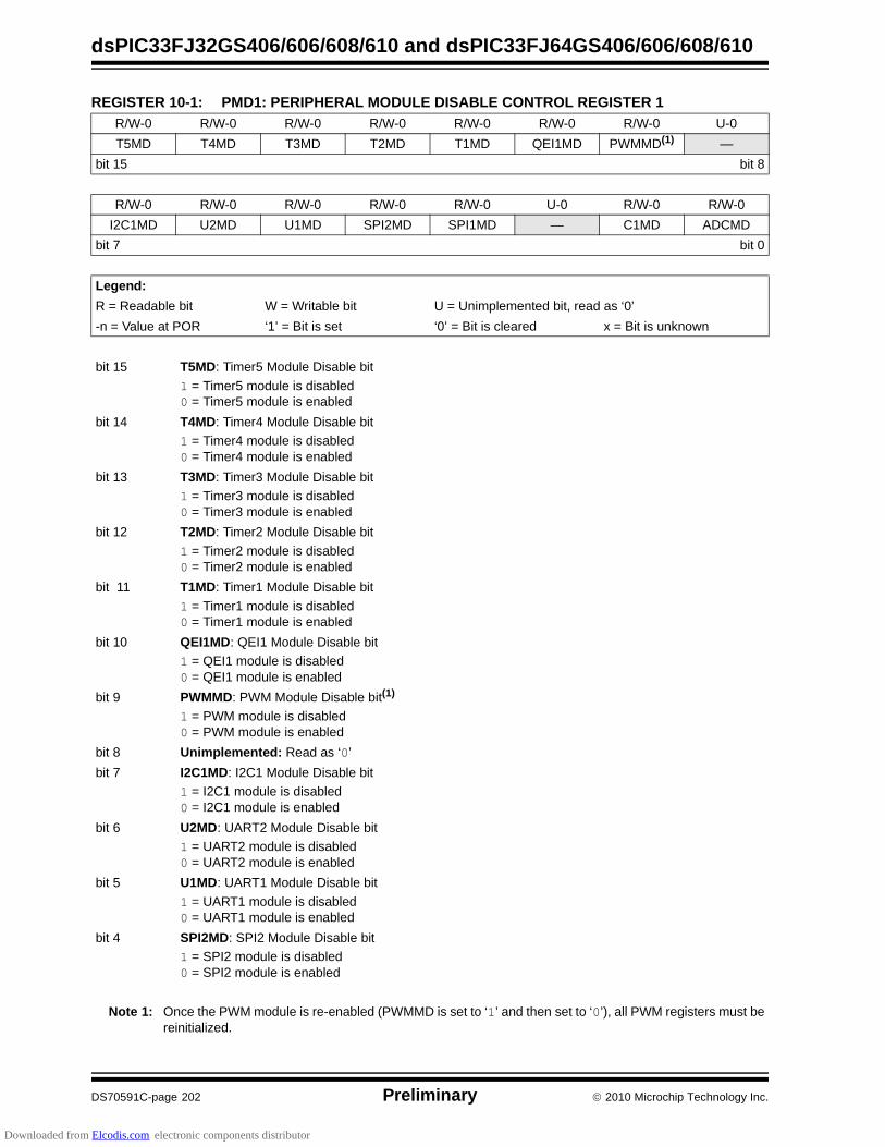
dsPIC33FJ32GS406/606/608/610 and dsPIC33FJ64GS406/606/608/610
DS70591C-page 202 Preliminary 2010 Microchip Technology Inc.
REGISTER 10-1: PMD1: PERIPHERAL MODULE DISABLE CONTROL REGISTER 1
R/W-0 R/W-0 R/W-0 R/W-0 R/W-0 R/W-0 R/W-0 U-0
T5MD T4MD T3MD T2MD T1MD QEI1MD PWMMD(1) —
bit 15 bit 8
R/W-0 R/W-0 R/W-0 R/W-0 R/W-0 U-0 R/W-0 R/W-0
I2C1MD U2MD U1MD SPI2MD SPI1MD — C1MD ADCMD
bit 7 bit 0
Legend:
R = Readable bit W = Writable bit U = Unimplemented bit, read as ‘0’
-n = Value at POR ‘1’ = Bit is set ‘0’ = Bit is cleared x = Bit is unknown
bit 15 T5MD: Timer5 Module Disable bit
1 = Timer5 module is disabled0 = Timer5 module is enabled
bit 14 T4MD: Timer4 Module Disable bit
1 = Timer4 module is disabled0 = Timer4 module is enabled
bit 13 T3MD: Timer3 Module Disable bit
1 = Timer3 module is disabled0 = Timer3 module is enabled
bit 12 T2MD: Timer2 Module Disable bit
1 = Timer2 module is disabled0 = Timer2 module is enabled
bit 11 T1MD: Timer1 Module Disable bit
1 = Timer1 module is disabled0 = Timer1 module is enabled
bit 10 QEI1MD: QEI1 Module Disable bit
1 = QEI1 module is disabled0 = QEI1 module is enabled
bit 9 PWMMD: PWM Module Disable bit(1)
1 = PWM module is disabled0 = PWM module is enabled
bit 8 Unimplemented: Read as ‘0’
bit 7 I2C1MD: I2C1 Module Disable bit
1 = I2C1 module is disabled0 = I2C1 module is enabled
bit 6 U2MD: UART2 Module Disable bit
1 = UART2 module is disabled0 = UART2 module is enabled
bit 5 U1MD: UART1 Module Disable bit
1 = UART1 module is disabled0 = UART1 module is enabled
bit 4 SPI2MD: SPI2 Module Disable bit
1 = SPI2 module is disabled0 = SPI2 module is enabled
Note 1: Once the PWM module is re-enabled (PWMMD is set to ‘1’ and then set to ‘0’), all PWM registers must bereinitialized.
Downloaded from Elcodis.com electronic components distributor
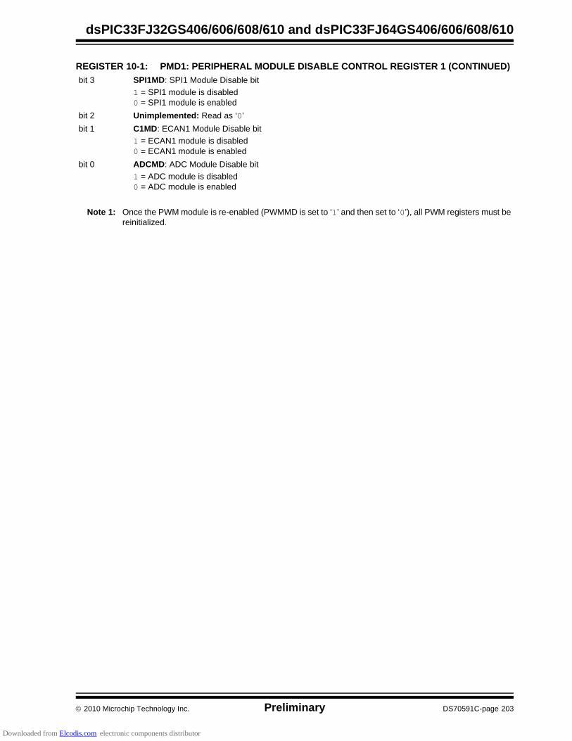
2010 Microchip Technology Inc. Preliminary DS70591C-page 203
dsPIC33FJ32GS406/606/608/610 and dsPIC33FJ64GS406/606/608/610
bit 3 SPI1MD: SPI1 Module Disable bit
1 = SPI1 module is disabled0 = SPI1 module is enabled
bit 2 Unimplemented: Read as ‘0’
bit 1 C1MD: ECAN1 Module Disable bit
1 = ECAN1 module is disabled0 = ECAN1 module is enabled
bit 0 ADCMD: ADC Module Disable bit
1 = ADC module is disabled0 = ADC module is enabled
REGISTER 10-1: PMD1: PERIPHERAL MODULE DISABLE CONTROL REGISTER 1 (CONTINUED)
Note 1: Once the PWM module is re-enabled (PWMMD is set to ‘1’ and then set to ‘0’), all PWM registers must bereinitialized.
Downloaded from Elcodis.com electronic components distributor
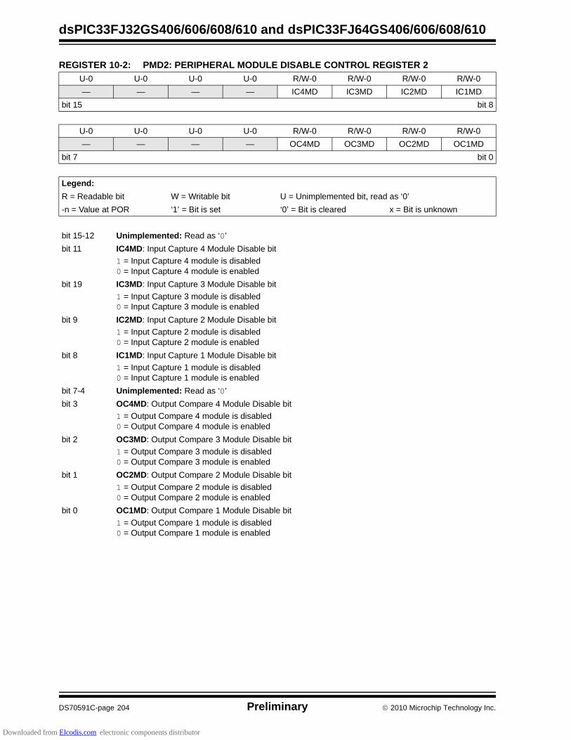
dsPIC33FJ32GS406/606/608/610 and dsPIC33FJ64GS406/606/608/610
DS70591C-page 204 Preliminary 2010 Microchip Technology Inc.
REGISTER 10-2: PMD2: PERIPHERAL MODULE DISABLE CONTROL REGISTER 2
U-0 U-0 U-0 U-0 R/W-0 R/W-0 R/W-0 R/W-0
— — — — IC4MD IC3MD IC2MD IC1MD
bit 15 bit 8
U-0 U-0 U-0 U-0 R/W-0 R/W-0 R/W-0 R/W-0
— — — — OC4MD OC3MD OC2MD OC1MD
bit 7 bit 0
Legend:
R = Readable bit W = Writable bit U = Unimplemented bit, read as ‘0’
-n = Value at POR ‘1’ = Bit is set ‘0’ = Bit is cleared x = Bit is unknown
bit 15-12 Unimplemented: Read as ‘0’
bit 11 IC4MD: Input Capture 4 Module Disable bit
1 = Input Capture 4 module is disabled0 = Input Capture 4 module is enabled
bit 19 IC3MD: Input Capture 3 Module Disable bit
1 = Input Capture 3 module is disabled0 = Input Capture 3 module is enabled
bit 9 IC2MD: Input Capture 2 Module Disable bit
1 = Input Capture 2 module is disabled0 = Input Capture 2 module is enabled
bit 8 IC1MD: Input Capture 1 Module Disable bit
1 = Input Capture 1 module is disabled0 = Input Capture 1 module is enabled
bit 7-4 Unimplemented: Read as ‘0’
bit 3 OC4MD: Output Compare 4 Module Disable bit
1 = Output Compare 4 module is disabled0 = Output Compare 4 module is enabled
bit 2 OC3MD: Output Compare 3 Module Disable bit
1 = Output Compare 3 module is disabled0 = Output Compare 3 module is enabled
bit 1 OC2MD: Output Compare 2 Module Disable bit
1 = Output Compare 2 module is disabled0 = Output Compare 2 module is enabled
bit 0 OC1MD: Output Compare 1 Module Disable bit
1 = Output Compare 1 module is disabled0 = Output Compare 1 module is enabled
Downloaded from Elcodis.com electronic components distributor

2010 Microchip Technology Inc. Preliminary DS70591C-page 205
dsPIC33FJ32GS406/606/608/610 and dsPIC33FJ64GS406/606/608/610
REGISTER 10-3: PMD3: PERIPHERAL MODULE DISABLE CONTROL REGISTER 3
REGISTER 10-4: PMD4: PERIPHERAL MODULE DISABLE CONTROL REGISTER 4
U-0 U-0 U-0 U-0 U-0 R/W-0 U-0 U-0
— — — — — CMPMD — —
bit 15 bit 8
U-0 U-0 R/W-0 U-0 U-0 U-0 R/W-0 U-0
— — QEI2MD — — — I2C2MD —
bit 7 bit 0
Legend:
R = Readable bit W = Writable bit U = Unimplemented bit, read as ‘0’
-n = Value at POR ‘1’ = Bit is set ‘0’ = Bit is cleared x = Bit is unknown
bit 15-11 Unimplemented: Read as ‘0’
bit 10 CMPMD: Analog Comparator Module Disable bit
1 = Analog Comparator module is disabled0 = Analog Comparator module is enabled
bit 9-6 Unimplemented: Read as ‘0’
bit 5 QEI2MD: QEI2 Module Disable bit
1 = QEI2 module is disabled0 = QEI2 module is enabled
bit 4-2 Unimplemented: Read as ‘0’
bit 1 I2C2MD: I2C2 Module Disable bit
1 = I2C2 module is disabled0 = I2C2 module is enabled
bit 0 Unimplemented: Read as ‘0’
U-0 U-0 U-0 U-0 U-0 U-0 U-0 U-0
— — — — — — — —
bit 15 bit 8
U-0 U-0 U-0 U-0 R/W-0 U-0 U-0 U-0
— — — — REFOMD — — —
bit 7 bit 0
Legend:
R = Readable bit W = Writable bit U = Unimplemented bit, read as ‘0’
-n = Value at POR ‘1’ = Bit is set ‘0’ = Bit is cleared x = Bit is unknown
bit 15-4 Unimplemented: Read as ‘0’
bit 3 REFOMD: Reference Clock Generator Module Disable bit
1 = Reference clock generator module is disabled0 = Reference clock generator module is enabled
bit 2-0 Unimplemented: Read as ‘0’
Downloaded from Elcodis.com electronic components distributor
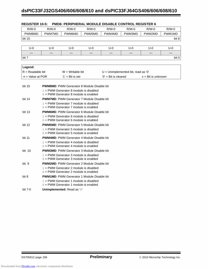
dsPIC33FJ32GS406/606/608/610 and dsPIC33FJ64GS406/606/608/610
DS70591C-page 206 Preliminary 2010 Microchip Technology Inc.
REGISTER 10-5: PMD6: PERIPHERAL MODULE DISABLE CONTROL REGISTER 6
R/W-0 R/W-0 R/W-0 R/W-0 R/W-0 R/W-0 R/W-0 R/W-0
PWM8MD PWM7MD PWM6MD PWM5MD PWM4MD PWM3MD PWM2MD PWM1MD
bit 15 bit 8
U-0 U-0 U-0 U-0 U-0 U-0 U-0 U-0
— — — — — — — —
bit 7 bit 0
Legend:
R = Readable bit W = Writable bit U = Unimplemented bit, read as ‘0’
-n = Value at POR ‘1’ = Bit is set ‘0’ = Bit is cleared x = Bit is unknown
bit 15 PWM8MD: PWM Generator 8 Module Disable bit
1 = PWM Generator 8 module is disabled0 = PWM Generator 8 module is enabled
bit 14 PWM7MD: PWM Generator 7 Module Disable bit
1 = PWM Generator 7 module is disabled0 = PWM Generator 7 module is enabled
bit 13 PWM6MD: PWM Generator 6 Module Disable bit
1 = PWM Generator 6 module is disabled0 = PWM Generator 6 module is enabled
bit 12 PWM5MD: PWM Generator 5 Module Disable bit
1 = PWM Generator 5 module is disabled0 = PWM Generator 5 module is enabled
bit 11 PWM4MD: PWM Generator 4 Module Disable bit
1 = PWM Generator 4 module is disabled0 = PWM Generator 4 module is enabled
bit 10 PWM3MD: PWM Generator 3 Module Disable bit
1 = PWM Generator 3 module is disabled0 = PWM Generator 3 module is enabled
bit 9 PWM2MD: PWM Generator 2 Module Disable bit
1 = PWM Generator 2 module is disabled0 = PWM Generator 2 module is enabled
bit 8 PWM1MD: PWM Generator 1 Module Disable bit
1 = PWM Generator 1 module is disabled0 = PWM Generator 1 module is enabled
bit 7-0 Unimplemented: Read as ‘0’
Downloaded from Elcodis.com electronic components distributor

2010 Microchip Technology Inc. Preliminary DS70591C-page 207
dsPIC33FJ32GS406/606/608/610 and dsPIC33FJ64GS406/606/608/610
REGISTER 10-6: PMD7: PERIPHERAL MODULE DISABLE CONTROL REGISTER 7
U-0 U-0 U-0 U-0 R/W-0 R/W-0 R/W-0 R/W-0
— — — — CMP4MD CMP3MD CMP2MD CMP1MD
bit 15 bit 8
U-0 U-0 U-0 U-0 U-0 U-0 U-0 R/W-0
— — — — — — — PWM9MD
bit 7 bit 0
Legend:
R = Readable bit W = Writable bit U = Unimplemented bit, read as ‘0’
-n = Value at POR ‘1’ = Bit is set ‘0’ = Bit is cleared x = Bit is unknown
bit 15-12 Unimplemented: Read as ‘0’
bit 11 CMP4MD: Analog Comparator 4 Module Disable bit
1 = Analog Comparator 4 module is disabled0 = Analog Comparator 4 module is enabled
bit 10 CMP3MD: Analog Comparator 3 Module Disable bit
1 = Analog Comparator 3 module is disabled0 = Analog Comparator 3 module is enabled
bit 9 CMP2MD: Analog Comparator 2 Module Disable bit
1 = Analog Comparator 2 module is disabled0 = Analog Comparator 2 module is enabled
bit 8 CMP1MD: Analog Comparator 1 Module Disable bit
1 = Analog Comparator 1 module is disabled0 = Analog Comparator 1 module is enabled
bit 7-1 Unimplemented: Read as ‘0’
bit 0 PWM9MD: PWM Generator 9 Module Disable bit
1 = PWM Generator 9 module is disabled0 = PWM Generator 9 module is enabled
Downloaded from Elcodis.com electronic components distributor

dsPIC33FJ32GS406/606/608/610 and dsPIC33FJ64GS406/606/608/610
DS70591C-page 208 Preliminary 2010 Microchip Technology Inc.
NOTES:
Downloaded from Elcodis.com electronic components distributor

2010 Microchip Technology Inc. Preliminary DS70591C-page 209
dsPIC33FJ32GS406/606/608/610 and dsPIC33FJ64GS406/606/608/610
11.0 I/O PORTS
All of the device pins (except VDD, VSS, MCLR andOSC1/CLKI) are shared among the peripherals and theparallel I/O ports. All I/O input ports feature SchmittTrigger inputs for improved noise immunity.
11.1 Parallel I/O (PIO) PortsGenerally a parallel I/O port that shares a pin with aperipheral is subservient to the peripheral. Theperipheral’s output buffer data and control signals areprovided to a pair of multiplexers. The multiplexersselect whether the peripheral or the associated port
has ownership of the output data and control signals ofthe I/O pin. The logic also prevents “loop through”, inwhich a port’s digital output can drive the input of aperipheral that shares the same pin. Figure 11-1 showshow ports are shared with other peripherals and theassociated I/O pin to which they are connected.
When a peripheral is enabled and the peripheral isactively driving an associated pin, the use of the pin asa general purpose output pin is disabled. The I/O pincan be read, but the output driver for the parallel port bitis disabled. If a peripheral is enabled, but the peripheralis not actively driving a pin, that pin can be driven by aport.
All port pins have three registers directly associatedwith their operation as digital I/O. The data directionregister (TRISx) determines whether the pin is an inputor an output. If the data direction bit is ‘1’, then the pinis an input. All port pins are defined as inputs after aReset. Reads from the latch (LATx) read the latch.Writes to the latch write the latch. Reads from the port(PORTx) read the port pins, while writes to the port pinswrite the latch.
Any bit and its associated data and control registersthat are not valid for a particular device will bedisabled. That means the corresponding LATx andTRISx registers and the port pin will read as zeros.
When a pin is shared with another peripheral orfunction that is defined as an input only, it isnevertheless regarded as a dedicated port becausethere is no other competing source of outputs.
FIGURE 11-1: BLOCK DIAGRAM OF A TYPICAL SHARED PORT STRUCTURE
Note 1: This data sheet summarizes the featuresof the dsPIC33FJ32GS406/606/608/610and dsPIC33FJ64GS406/606/608/610families of devices. It is not intended to bea comprehensive reference source. Tocomplement the information in this datasheet, refer to Section 10. “I/O Ports”(DS70193) in the “dsPIC33F/PIC24HFamily Reference Manual”, which is avail-able from the Microchip web site(www.microchip.com).
2: Some registers and associated bitsdescribed in this section may not be avail-able on all devices. Refer to Section 4.0“Memory Organization” in this datasheet for device-specific register and bitinformation.
QD
CK
WR LAT +
TRIS Latch
I/O Pin
WR PORT
Data Bus
QD
CK
Data Latch
Read PORT
Read TRIS
1
0
1
0
WR TRIS
Peripheral Output DataOutput Enable
Peripheral Input Data
I/O
Peripheral Module
Peripheral Output Enable
PIO Module
Output Multiplexers
Output Data
Input Data
Peripheral Module Enable
Read LAT
Downloaded from Elcodis.com electronic components distributor

dsPIC33FJ32GS406/606/608/610 and dsPIC33FJ64GS406/606/608/610
DS70591C-page 210 Preliminary 2010 Microchip Technology Inc.
11.2 Open-Drain Configuration
In addition to the PORT, LAT and TRIS registers fordata control, some digital-only port pins can also beindividually configured for either digital or open-drainoutput. This is controlled by the Open-Drain Controlregister, ODCx, associated with each port. Setting anyof the bits configures the corresponding pin to act as anopen-drain output.
The open-drain feature allows the generation ofoutputs higher than VDD (for example, 5V) on anydesired 5V tolerant pins by using external pull-upresistors. The maximum open-drain voltage allowed isthe same as the maximum VIH specification.
Refer to “Pin Diagrams” for the available pins andtheir functionality.
11.3 Configuring Analog Port Pins
The ADPCFG and TRIS registers control the operationof the Analog-to-Digital (A/D) port pins. The port pinsthat are to function as analog inputs must have theircorresponding TRIS bit set (input). If the TRIS bit iscleared (output), the digital output level (VOH or VOL)will be converted.
The ADPCFG and ADPCFG2 registers have a defaultvalue of 0x000; therefore, all pins that share ANxfunctions are analog (not digital) by default.
When the PORT register is read, all pins configured asanalog input channels will read as cleared (a low level).
Pins configured as digital inputs will not convert ananalog input. Analog levels on any pin defined as adigital input (including the ANx pins) can cause theinput buffer to consume current that exceeds thedevice specifications.
11.4 I/O Port Write/Read Timing
One instruction cycle is required between a port directionchange or port write operation and a read operation ofthe same port. Typically, this instruction would be a NOP.An example is shown in Example 11-1.
11.5 Input Change Notification
The input change notification function of the I/Oports allows the dsPIC33FJ32GS406/606/608/610and dsPIC33FJ64GS406/606/608/610 devices to gen-erate interrupt requests to the processor in response toa Change-Of-State (COS) on selected input pins. Thisfeature can detect input Change-Of-States even inSleep mode, when the clocks are disabled. Dependingon the device pin count, up to 30 external signals (CNxpin) can be selected (enabled) for generating aninterrupt request on a Change-Of-State.
Four control registers are associated with the CNmodule. The CNEN1 and CNEN2 registers contain theinterrupt enable control bits for each of the CN inputpins. Setting any of these bits enables a CN interruptfor the corresponding pins.
Each CN pin also has a weak pull-up connected to it.The pull-ups act as a current source connected to thepin, and eliminate the need for external resistors whenthe push button or keypad devices are connected. Thepull-ups are enabled separately using the CNPU1 andCNPU2 registers, which contain the control bits foreach of the CN pins. Setting any of the control bitsenables the weak pull-ups for the corresponding pins.
EQUATION 11-1: PORT WRITE/READ EXAMPLE
Note: Pull-ups on change notification pinsshould always be disabled when the portpin is configured as a digital output.
MOV 0xFF00, W0 ; Configure PORTB<15:8> as inputsMOV W0, TRISBB ; and PORTB<7:0> as outputsNOP ; Delay 1 cycleBTSS PORTB, #13 ; Next Instruction
Downloaded from Elcodis.com electronic components distributor

2010 Microchip Technology Inc. Preliminary DS70591C-page 211
dsPIC33FJ32GS406/606/608/610 and dsPIC33FJ64GS406/606/608/610
12.0 TIMER1
The Timer1 module is a 16-bit timer, which can serveas a time counter for the Real-Time Clock (RTC), oroperate as a free-running interval timer/counter.
The Timer1 module has the following unique featuresover other timers:
• Can be operated from the low-power 32.767 kHz crystal oscillator available on the device
• Can be operated in Asynchronous Counter mode from an external clock source.
• The external clock input (T1CK) can optionally be synchronized to the internal device clock and the clock synchronization is performed after the prescaler.
The unique features of Timer1 allow it to be used forReal-Time Clock (RTC) applications. A block diagramof Timer1 is shown in Figure 12-1.
The Timer1 module can operate in one of the followingmodes:
• Timer mode• Gated Timer mode• Synchronous Counter mode• Asynchronous Counter mode
In Timer and Gated Timer modes, the input clock isderived from the internal instruction cycle clock (FCY).In Synchronous and Asynchronous Counter modes,the input clock is derived from the external clock inputat the T1CK pin.
The Timer modes are determined by the following bits:
• Timer Clock Source Control bit (TCS): T1CON<1>
• Timer Synchronization Control bit (TSYNC): T1CON<2>
• Timer Gate Control bit (TGATE): T1CON<6>
The timer control bit settings for different operatingmodes are given in the Table 12-1.
TABLE 12-1: TIMER MODE SETTINGS
FIGURE 12-1: 16-BIT TIMER1 MODULE BLOCK DIAGRAM
Note 1: This data sheet summarizes the featuresof the dsPIC33FJ32GS406/606/608/610and dsPIC33FJ64GS406/606/608/610families of devices. It is not intended to bea comprehensive reference source. Tocomplement the information in this datasheet, refer to Section 11. “Timers”(DS70205) in the “dsPIC33F/PIC24HFamily Reference Manual”, which is avail-able from the Microchip web site(www.microchip.com).
2: Some registers and associated bitsdescribed in this section may not be avail-able on all devices. Refer to Section 4.0“Memory Organization” in this datasheet for device-specific register and bitinformation.
Mode TCS TGATE TSYNC
Timer 0 0 x
Gated Timer 0 1 x
Synchronous Counter
1 x 1
Asynchronous Counter
1 x 0
TGATE
TCS
00
10
x1
TMR1
Comparator
PR1
TGATE
Set T1IF Flag
0
1
TSYNC
0
1
SyncEqual
Reset
T1CKPrescaler
(/n)
TCKPS<1:0>
GateSync
FCY
Falling EdgeDetect
Prescaler(/n)
TCKPS<1:0>
Downloaded from Elcodis.com electronic components distributor

dsPIC33FJ32GS406/606/608/610 and dsPIC33FJ64GS406/606/608/610
DS70591C-page 212 Preliminary 2010 Microchip Technology Inc.
REGISTER 12-1: T1CON: TIMER1 CONTROL REGISTER
R/W-0 U-0 R/W-0 U-0 U-0 U-0 U-0 U-0
TON — TSIDL — — — — —
bit 15 bit 8
U-0 R/W-0 R/W-0 R/W-0 U-0 R/W-0 R/W-0 U-0
— TGATE TCKPS<1:0> — TSYNC TCS —
bit 7 bit 0
Legend:
R = Readable bit W = Writable bit U = Unimplemented bit, read as ‘0’
-n = Value at POR ‘1’ = Bit is set ‘0’ = Bit is cleared x = Bit is unknown
bit 15 TON: Timer1 On bit
1 = Starts 16-bit Timer10 = Stops 16-bit Timer1
bit 14 Unimplemented: Read as ‘0’
bit 13 TSIDL: Stop in Idle Mode bit
1 = Discontinue module operation when device enters Idle mode0 = Continue module operation in Idle mode
bit 12-7 Unimplemented: Read as ‘0’
bit 6 TGATE: Timer1 Gated Time Accumulation Enable bit
When T1CS = 1: This bit is ignored.
When T1CS = 0: 1 = Gated time accumulation enabled0 = Gated time accumulation disabled
bit 5-4 TCKPS<1:0> Timer1 Input Clock Prescale Select bits
11 = 1:256 10 = 1:6401 = 1:8 00 = 1:1
bit 3 Unimplemented: Read as ‘0’
bit 2 TSYNC: Timer1 External Clock Input Synchronization Select bit
When TCS = 1: 1 = Synchronize external clock input0 = Do not synchronize external clock input
When TCS = 0: This bit is ignored.
bit 1 TCS: Timer1 Clock Source Select bit
1 = External clock from T1CK pin (on the rising edge) 0 = Internal clock (FCY)
bit 0 Unimplemented: Read as ‘0’
Downloaded from Elcodis.com electronic components distributor
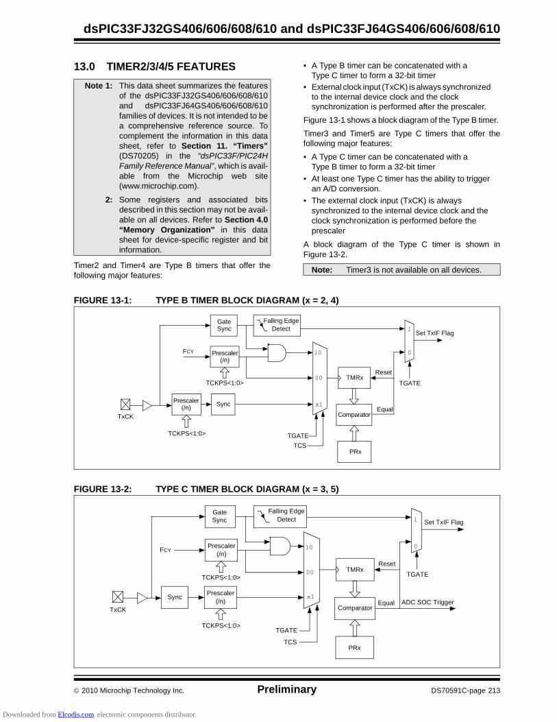
2010 Microchip Technology Inc. Preliminary DS70591C-page 213
dsPIC33FJ32GS406/606/608/610 and dsPIC33FJ64GS406/606/608/610
13.0 TIMER2/3/4/5 FEATURES
Timer2 and Timer4 are Type B timers that offer thefollowing major features:
• A Type B timer can be concatenated with a Type C timer to form a 32-bit timer
• External clock input (TxCK) is always synchronized to the internal device clock and the clock synchronization is performed after the prescaler.
Figure 13-1 shows a block diagram of the Type B timer.
Timer3 and Timer5 are Type C timers that offer thefollowing major features:
• A Type C timer can be concatenated with a Type B timer to form a 32-bit timer
• At least one Type C timer has the ability to trigger an A/D conversion.
• The external clock input (TxCK) is always synchronized to the internal device clock and the clock synchronization is performed before the prescaler
A block diagram of the Type C timer is shown inFigure 13-2.
FIGURE 13-1: TYPE B TIMER BLOCK DIAGRAM (x = 2, 4)
FIGURE 13-2: TYPE C TIMER BLOCK DIAGRAM (x = 3, 5)
Note 1: This data sheet summarizes the featuresof the dsPIC33FJ32GS406/606/608/610and dsPIC33FJ64GS406/606/608/610families of devices. It is not intended to bea comprehensive reference source. Tocomplement the information in this datasheet, refer to Section 11. “Timers”(DS70205) in the “dsPIC33F/PIC24HFamily Reference Manual”, which is avail-able from the Microchip web site(www.microchip.com).
2: Some registers and associated bitsdescribed in this section may not be avail-able on all devices. Refer to Section 4.0“Memory Organization” in this datasheet for device-specific register and bitinformation.
Note: Timer3 is not available on all devices.
Prescaler(/n)
TGATE
TCS
00
10
x1
TMRx
Comparator
PRx
TGATE
Set TxIF Flag
0
1
Sync
TCKPS<1:0>
Equal
Reset
TxCK
GateSync
FCY
Falling EdgeDetect
Prescaler(/n)
TCKPS<1:0>
Prescaler(/n)
GateSync
TGATE
TCS
00
10
x1
TMRx
Comparator
PRx
FCY
TGATE
Falling Edge Detect Set TxIF Flag
0
1
Sync
TCKPS<1:0>
Equal
Reset
TxCKADC SOC Trigger
Prescaler(/n)
TCKPS<1:0>
Downloaded from Elcodis.com electronic components distributor

dsPIC33FJ32GS406/606/608/610 and dsPIC33FJ64GS406/606/608/610
DS70591C-page 214 Preliminary 2010 Microchip Technology Inc.
The Timer2/3/4/5 modules can operate in one of thefollowing modes:
• Timer mode• Gated Timer mode• Synchronous Counter mode
In Timer and Gated Timer modes, the input clock isderived from the internal instruction cycle clock (FCY).In Synchronous Counter mode, the input clock isderived from the external clock input at the TxCK pin.
The timer modes are determined by the following bits:
• TCS (TxCON<1>): Timer Clock Source Control bit• TGATE (TxCON<6>): Timer Gate Control bit
Timer control bit settings for different operating modesare given in the Table 13-1.
TABLE 13-1: TIMER MODE SETTINGS
13.1 16-Bit Operation
To configure any of the timers for individual 16-bitoperation:
1. Clear the T32 bit corresponding to that timer.
2. Select the timer prescaler ratio using theTCKPS<1:0> bits.
3. Set the Clock and Gating modes using the TCSand TGATE bits.
4. Load the timer period value into the PRxregister.
5. If interrupts are required, set the interrupt enablebit, TxIE. Use the priority bits, TxIP<2:0>, to setthe interrupt priority.
6. Set the TON bit.
13.2 32-Bit Operation
A 32-bit timer module can be formed by combining aType B and a Type C 16-bit timer module. For 32-bittimer operation, the T32 control bit in the Type B TimerControl (TxCON<3>) register must be set. The Type Ctimer holds the most significant word (msw) and theType B timer holds the least significant word (lsw)for 32-bit operation.
When configured for 32-bit operation, only the Type BTimer Control (TxCON) register bits are required forsetup and control while the Type C Timer Controlregister bits are ignored (except the TSIDL bit).
For interrupt control, the combined 32-bit timer usesthe interrupt enable, interrupt flag and interrupt prioritycontrol bits of the Type C timer. The interrupt controland status bits for the Type B timer are ignoredduring 32-bit timer operation.
The timers that can be combined to form a 32-bit timerare listed in Table 13-2.
TABLE 13-2: 32-BIT TIMER
A block diagram representation of the 32-bit timermodule is shown in Figure 13-3. The 32-timer modulecan operate in one of the following modes:
• Timer mode• Gated Timer mode• Synchronous Counter mode
To configure the timer features for 32-bit operation:
1. Set the T32 control bit.
2. Select the prescaler ratio for Timer2 using theTCKPS<1:0> bits.
3. Set the Clock and Gating modes using thecorresponding TCS and TGATE bits.
4. Load the timer period value. PR3 contains themost significant word of the value, while PR2contains the least significant word.
5. If interrupts are required, set the interrupt enablebit, T3IE. Use the priority bits, T3IP<2:0>, to setthe interrupt priority. While Timer2 controls thetimer, the interrupt appears as a Timer3interrupt.
6. Set the corresponding TON bit.
Mode TCS TGATE
Timer 0 0
Gated Timer 0 1
Synchronous Counter 1 x
Type B Timer (lsw) Type C Timer (msw)
Timer2 Timer3
TImer4 Timer5
Downloaded from Elcodis.com electronic components distributor

2010 Microchip Technology Inc. Preliminary DS70591C-page 215
dsPIC33FJ32GS406/606/608/610 and dsPIC33FJ64GS406/606/608/610
FIGURE 13-3: 32-BIT TIMER BLOCK DIAGRAM
Prescaler(/n)
TGATE
TCS
00
10
x1
TMRx(1)
PRx
TGATE
Set TyIF
0
1
Sync
TCKPS<1:0>
Equal
TxCK
GateSync
FCY
Falling Edge Detect
Prescaler(/n)
TCKPS<1:0>TMRy(2)
Comparator
PRy
Reset
mswlsw
TMRyHLD
Data Bus <15:0>
Flag
Note 1: Timerx is a Type B Timer (x = 2, 4).
2: Timery is a Type C Timer (y = 3, 5).
Downloaded from Elcodis.com electronic components distributor

dsPIC33FJ32GS406/606/608/610 and dsPIC33FJ64GS406/606/608/610
DS70591C-page 216 Preliminary 2010 Microchip Technology Inc.
REGISTER 13-1: TxCON: TIMER CONTROL REGISTER (x = 2, 4)
R/W-0 U-0 R/W-0 U-0 U-0 U-0 U-0 U-0
TON — TSIDL — — — — —
bit 15 bit 8
U-0 R/W-0 R/W-0 R/W-0 R/W-0 U-0 R/W-0 U-0
— TGATE TCKPS<1:0> T32 — TCS —
bit 7 bit 0
Legend:
R = Readable bit W = Writable bit U = Unimplemented bit, read as ‘0’
-n = Value at POR ‘1’ = Bit is set ‘0’ = Bit is cleared x = Bit is unknown
bit 15 TON: Timerx On bit
When T32 = 1 (in 32-Bit Timer mode):1 = Starts 32-bit TMRx:TMRy timer pair0 = Stops 32-bit TMRx:TMRy timer pair
When T32 = 0 (in 16-Bit Timer mode):1 = Starts 16-bit timer0 = Stops 16-bit timer
bit 14 Unimplemented: Read as ‘0’
bit 13 TSIDL: Stop in Idle Mode bit
1 = Discontinue timer operation when device enters Idle mode0 = Continue timer operation in Idle mode
bit 12-7 Unimplemented: Read as ‘0’
bit 6 TGATE: Timerx Gated Time Accumulation Enable bit
When TCS = 1:This bit is ignored.
When TCS = 0:1 = Gated time accumulation enabled0 = Gated time accumulation disabled
bit 5-4 TCKPS<1:0>: Timerx Input Clock Prescale Select bits
11 = 1:256 prescale value10 = 1:64 prescale value01 = 1:8 prescale value00 = 1:1 prescale value
bit 3 T32: 32-Bit Timerx Mode Select bit
1 = TMRx and TMRy form a 32-bit timer0 = TMRx and TMRy form separate 16-bit timer
bit 2 Unimplemented: Read as ‘0’
bit 1 TCS: Timerx Clock Source Select bit
1 = External clock from TxCK pin0 = Internal clock (FOSC/2)
bit 0 Unimplemented: Read as ‘0’
Downloaded from Elcodis.com electronic components distributor
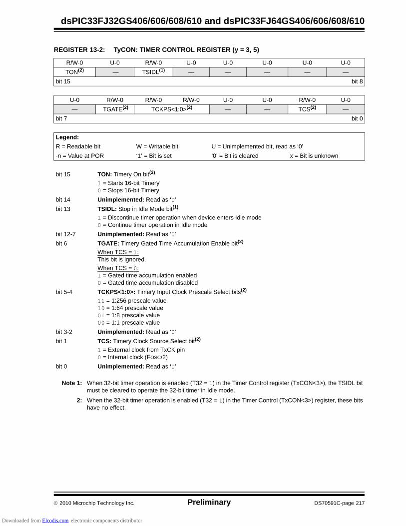
2010 Microchip Technology Inc. Preliminary DS70591C-page 217
dsPIC33FJ32GS406/606/608/610 and dsPIC33FJ64GS406/606/608/610
REGISTER 13-2: TyCON: TIMER CONTROL REGISTER (y = 3, 5)
R/W-0 U-0 R/W-0 U-0 U-0 U-0 U-0 U-0
TON(2) — TSIDL(1) — — — — —
bit 15 bit 8
U-0 R/W-0 R/W-0 R/W-0 U-0 U-0 R/W-0 U-0
— TGATE(2) TCKPS<1:0>(2) — — TCS(2) —
bit 7 bit 0
Legend:
R = Readable bit W = Writable bit U = Unimplemented bit, read as ‘0’
-n = Value at POR ‘1’ = Bit is set ‘0’ = Bit is cleared x = Bit is unknown
bit 15 TON: Timery On bit(2)
1 = Starts 16-bit Timery0 = Stops 16-bit Timery
bit 14 Unimplemented: Read as ‘0’
bit 13 TSIDL: Stop in Idle Mode bit(1)
1 = Discontinue timer operation when device enters Idle mode0 = Continue timer operation in Idle mode
bit 12-7 Unimplemented: Read as ‘0’
bit 6 TGATE: Timery Gated Time Accumulation Enable bit(2)
When TCS = 1:This bit is ignored.
When TCS = 0:1 = Gated time accumulation enabled0 = Gated time accumulation disabled
bit 5-4 TCKPS<1:0>: Timery Input Clock Prescale Select bits(2)
11 = 1:256 prescale value10 = 1:64 prescale value01 = 1:8 prescale value00 = 1:1 prescale value
bit 3-2 Unimplemented: Read as ‘0’
bit 1 TCS: Timery Clock Source Select bit(2)
1 = External clock from TxCK pin0 = Internal clock (FOSC/2)
bit 0 Unimplemented: Read as ‘0’
Note 1: When 32-bit timer operation is enabled (T32 = 1) in the Timer Control register (TxCON<3>), the TSIDL bitmust be cleared to operate the 32-bit timer in Idle mode.
2: When the 32-bit timer operation is enabled (T32 = 1) in the Timer Control (TxCON<3>) register, these bitshave no effect.
Downloaded from Elcodis.com electronic components distributor

dsPIC33FJ32GS406/606/608/610 and dsPIC33FJ64GS406/606/608/610
DS70591C-page 218 Preliminary 2010 Microchip Technology Inc.
NOTES:
Downloaded from Elcodis.com electronic components distributor

2010 Microchip Technology Inc. Preliminary DS70591C-page 219
dsPIC33FJ32GS406/606/608/610 and dsPIC33FJ64GS406/606/608/610
14.0 INPUT CAPTURE
The input capture module is useful in applicationsrequiring frequency (period) and pulse measurement.The dsPIC33FJ32GS406/606/608/610 anddsPIC33FJ64GS406/606/608/610 devices support up totwo input capture channels.
The input capture module captures the 16-bit value ofthe selected Time Base register when an event occursat the ICx pin. The events that cause a capture eventare listed below in three categories:
• Simple Capture Event modes:
- Capture timer value on every falling edge of input at ICx pin
- Capture timer value on every rising edge of input at ICx pin
• Capture timer value on every edge (rising and falling)
• Prescaler Capture Event modes:
- Capture timer value on every 4th rising edge of input at ICx pin
- Capture timer value on every 16th rising edge of input at ICx pin
Each input capture channel can select one of thetwo 16-bit timers (Timer2 or Timer3) for the timebase. The selected timer can use either an internalor external clock.
Other operational features include:
• Device wake-up from capture pin during CPU Sleep and Idle modes
• Interrupt on input capture event
• 4-word FIFO buffer for capture values
- Interrupt optionally generated after 1, 2, 3 or 4 buffer locations are filled
• Use of input capture to provide additional sources of external interrupts
FIGURE 14-1: INPUT CAPTURE BLOCK DIAGRAM
Note 1: This data sheet summarizes the featuresof the dsPIC33FJ32GS406/606/608/610and dsPIC33FJ64GS406/606/608/610families of devices. It is not intended to bea comprehensive reference source. Tocomplement the information in this datasheet, refer to Section 12. “Input Cap-ture” (DS70198) in the “dsPIC33F/PIC24H Family Reference Manual”,which is available from the Microchip website (www.microchip.com).
2: Some registers and associated bitsdescribed in this section may not be avail-able on all devices. Refer to Section 4.0“Memory Organization” in this datasheet for device-specific register and bitinformation.
ICxBUF
ICx PinICM<2:0> (ICxCON<2:0>)
Mode Select3
1 0
Set Flag ICxIF(in IFSx Register)
TMR2 TMR3
Edge Detection Logic
16 16
FIFOR/WLogic
ICxI<1:0>
ICOV, ICBNE (ICxCON<4:3>)
ICxCONInterrupt
Logic
System Bus
From 16-Bit Timers
ICTMR(ICxCON<7>)
FIF
O
PrescalerCounter(1, 4, 16)
andClock Synchronizer
Note 1: An ‘x’ in a signal, register or bit name denotes the number of the capture channel.
Downloaded from Elcodis.com electronic components distributor

dsPIC33FJ32GS406/606/608/610 and dsPIC33FJ64GS406/606/608/610
DS70591C-page 220 Preliminary 2010 Microchip Technology Inc.
14.1 Input Capture Registers
REGISTER 14-1: ICxCON: INPUT CAPTURE x CONTROL REGISTER (x = 1, 2)
U-0 U-0 R/W-0 U-0 U-0 U-0 U-0 U-0
— — ICSIDL — — — — —
bit 15 bit 8
R/W-0 R/W-0 R/W-0 R-0, HC R-0, HC R/W-0 R/W-0 R/W-0
ICTMR ICI<1:0> ICOV ICBNE ICM<2:0>
bit 7 bit 0
Legend: HC = Hardware Clearable bit
R = Readable bit W = Writable bit U = Unimplemented bit, read as ‘0’
-n = Value at POR ‘1’ = Bit is set ‘0’ = Bit is cleared x = Bit is unknown
bit 15-14 Unimplemented: Read as ‘0’
bit 13 ICSIDL: Input Capture Module Stop in Idle Control bit
1 = Input capture module halts in CPU Idle mode0 = Input capture module continues to operate in CPU Idle mode
bit 12-8 Unimplemented: Read as ‘0’
bit 7 ICTMR: Input Capture Timer Select bits
1 = TMR2 contents are captured on capture event0 = TMR3 contents are captured on capture event
bit 6-5 ICI<1:0>: Select Number of Captures per Interrupt bits
11 = Interrupt on every fourth capture event10 = Interrupt on every third capture event01 = Interrupt on every second capture event00 = Interrupt on every capture event
bit 4 ICOV: Input Capture Overflow Status Flag bit (read-only)
1 = Input capture overflow occurred0 = No input capture overflow occurred
bit 3 ICBNE: Input Capture Buffer Empty Status bit (read-only)
1 = Input capture buffer is not empty, at least one more capture value can be read0 = Input capture buffer is empty
bit 2-0 ICM<2:0>: Input Capture Mode Select bits
111 = Input capture functions as interrupt pin only when device is in Sleep or Idle mode. Rising edgedetect-only, all other control bits are not applicable.
110 = Unused (module disabled)101 = Capture mode, every 16th rising edge100 = Capture mode, every 4th rising edge011 = Capture mode, every rising edge010 = Capture mode, every falling edge001 = Capture mode, every edge (rising and falling). ICI<1:0> bits do not control interrupt generation
for this mode.000 = Input capture module turned off
Downloaded from Elcodis.com electronic components distributor

2010 Microchip Technology Inc. Preliminary DS70591C-page 221
dsPIC33FJ32GS406/606/608/610 and dsPIC33FJ64GS406/606/608/610
15.0 OUTPUT COMPARE The output compare module can select either Timer2 orTimer3 for its time base. The module compares thevalue of the timer with the value of one or two Compareregisters depending on the operating mode selected.The state of the output pin changes when the timervalue matches the Compare register value. The outputcompare module generates either a single outputpulse, or a sequence of output pulses, by changing thestate of the output pin on the compare match events.The output compare module can also generateinterrupts on compare match events.
The output compare module has multiple operatingmodes:
• Active-Low One-Shot mode• Active-High One-Shot mode• Toggle mode• Delayed One-Shot mode• Continuous Pulse mode• PWM mode without Fault Protection• PWM mode with Fault Protection
FIGURE 15-1: OUTPUT COMPARE MODULE BLOCK DIAGRAM
Note 1: This data sheet summarizes the featuresof the dsPIC33FJ32GS406/606/608/610and dsPIC33FJ64GS406/606/608/610families of devices. It is not intended to bea comprehensive reference source. Tocomplement the information in this datasheet, refer to Section 13. “OutputCompare” (DS70209) in the “dsPIC33F/PIC24H Family Reference Manual”,which is available from the Microchip website (www.microchip.com).
2: Some registers and associated bitsdescribed in this section may not be avail-able on all devices. Refer to Section 4.0“Memory Organization” in this datasheet for device-specific register and bitinformation.
OCxR
Comparator
OutputLogic
OCM<2:0>
Output Enable
OCx
Set Flag bitOCxIF
OCxRS
Mode Select
3
0 1 OCTSEL 0 1
16 16
OCFA
TMR2 TMR2
QSR
TMR3 TMR3Rollover Rollover
Note: An ‘x’ in a signal, register or bit name denotes the number of the output compare channels.
Downloaded from Elcodis.com electronic components distributor
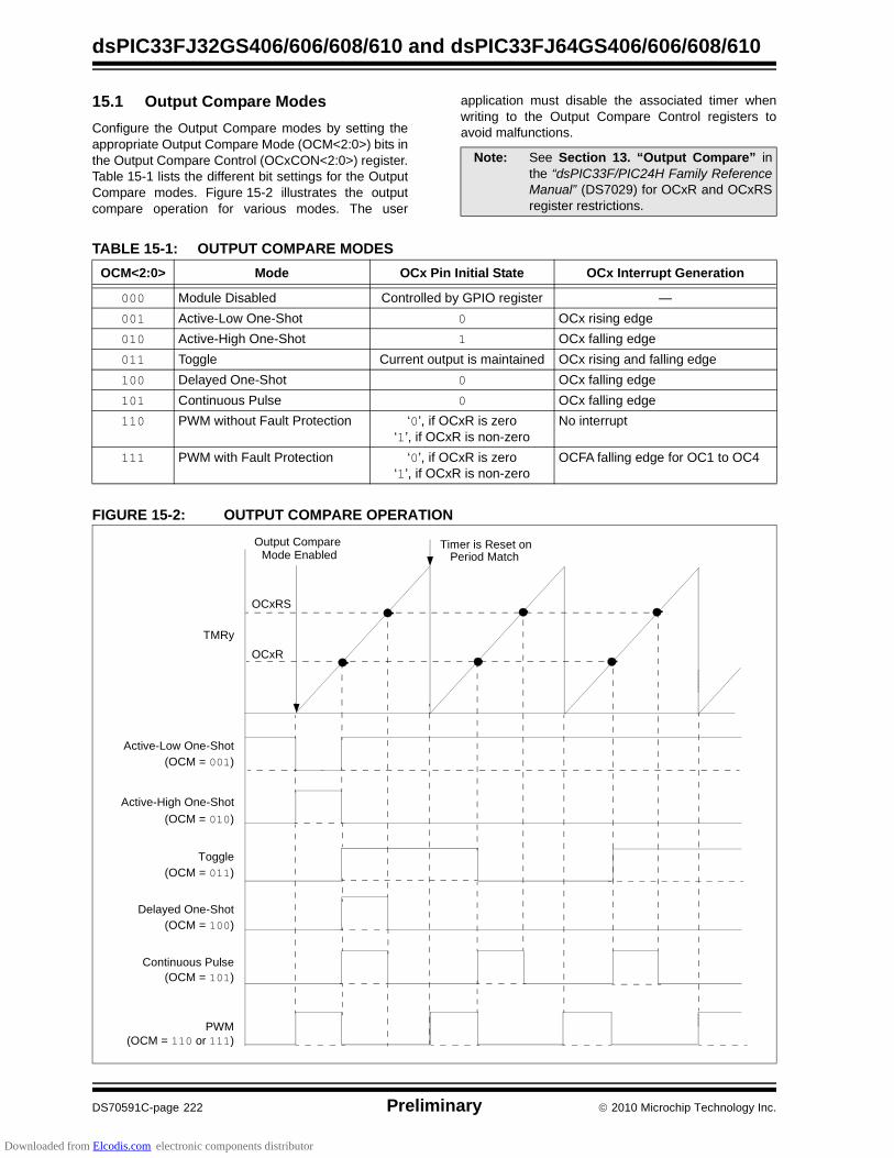
dsPIC33FJ32GS406/606/608/610 and dsPIC33FJ64GS406/606/608/610
DS70591C-page 222 Preliminary 2010 Microchip Technology Inc.
15.1 Output Compare Modes
Configure the Output Compare modes by setting theappropriate Output Compare Mode (OCM<2:0>) bits inthe Output Compare Control (OCxCON<2:0>) register.Table 15-1 lists the different bit settings for the OutputCompare modes. Figure 15-2 illustrates the outputcompare operation for various modes. The user
application must disable the associated timer whenwriting to the Output Compare Control registers toavoid malfunctions.
TABLE 15-1: OUTPUT COMPARE MODES
FIGURE 15-2: OUTPUT COMPARE OPERATION
Note: See Section 13. “Output Compare” inthe “dsPIC33F/PIC24H Family ReferenceManual” (DS7029) for OCxR and OCxRSregister restrictions.
OCM<2:0> Mode OCx Pin Initial State OCx Interrupt Generation
000 Module Disabled Controlled by GPIO register —
001 Active-Low One-Shot 0 OCx rising edge
010 Active-High One-Shot 1 OCx falling edge
011 Toggle Current output is maintained OCx rising and falling edge
100 Delayed One-Shot 0 OCx falling edge
101 Continuous Pulse 0 OCx falling edge
110 PWM without Fault Protection ‘0’, if OCxR is zero‘1’, if OCxR is non-zero
No interrupt
111 PWM with Fault Protection ‘0’, if OCxR is zero‘1’, if OCxR is non-zero
OCFA falling edge for OC1 to OC4
OCxRS
TMRy
OCxR
Timer is Reset onPeriod Match
Continuous Pulse(OCM = 101)
PWM(OCM = 110 or 111)
Active-Low One-Shot(OCM = 001)
Active-High One-Shot
(OCM = 010)
Toggle(OCM = 011)
Delayed One-Shot(OCM = 100)
Output Compare Mode Enabled
Downloaded from Elcodis.com electronic components distributor

2010 Microchip Technology Inc. Preliminary DS70591C-page 223
dsPIC33FJ32GS406/606/608/610 and dsPIC33FJ64GS406/606/608/610
REGISTER 15-1: OCxCON: OUTPUT COMPARE x CONTROL REGISTER (x = 1, 2)
U-0 U-0 R/W-0 U-0 U-0 U-0 U-0 U-0
— — OCSIDL — — — — —
bit 15 bit 8
U-0 U-0 U-0 R-0, HC R/W-0 R/W-0 R/W-0 R/W-0
— — — OCFLT OCTSEL OCM<2:0>
bit 7 bit 0
Legend: HC = Hardware Clearable bit
R = Readable bit W = Writable bit U = Unimplemented bit, read as ‘0’
-n = Value at POR ‘1’ = Bit is set ‘0’ = Bit is cleared x = Bit is unknown
bit 15-14 Unimplemented: Read as ‘0’
bit 13 OCSIDL: Stop Output Compare in Idle Mode Control bit
1 = Output Compare x halts in CPU Idle mode0 = Output Compare x continues to operate in CPU Idle mode
bit 12-5 Unimplemented: Read as ‘0’
bit 4 OCFLT: PWM Fault Condition Status bit
1 = PWM Fault condition has occurred (cleared in hardware only)0 = No PWM Fault condition has occurred (this bit is only used when OCM<2:0> = 111)
bit 3 OCTSEL: Output Compare Timer Select bit
1 = Timer3 is the clock source for Compare x0 = Timer2 is the clock source for Compare x
bit 2-0 OCM<2:0>: Output Compare Mode Select bits
111 = PWM mode on OCx, Fault pin enabled110 = PWM mode on OCx, Fault pin disabled101 = Initialize OCx pin low, generate continuous output pulses on OCx pin100 = Initialize OCx pin low, generate single output pulse on OCx pin011 = Compare event toggles OCx pin010 = Initialize OCx pin high, compare event forces OCx pin low001 = Initialize OCx pin low, compare event forces OCx pin high 000 = Output compare channel is disabled
Downloaded from Elcodis.com electronic components distributor

dsPIC33FJ32GS406/606/608/610 and dsPIC33FJ64GS406/606/608/610
DS70591C-page 224 Preliminary 2010 Microchip Technology Inc.
NOTES:
Downloaded from Elcodis.com electronic components distributor
2010 Microchip Technology Inc. Preliminary DS70591C-page 225
dsPIC33FJ32GS406/606/608/610 and dsPIC33FJ64GS406/606/608/610
16.0 HIGH-SPEED PWM
The High-Speed PWM module on thedsPIC33FJ32GS406/606/608/610 anddsPIC33FJ64GS406/606/608/610 devices supports awide variety of PWM modes and output formats. ThisPWM module is ideal for power conversion applica-tions, such as:
• AC/DC Converters• DC/DC Converters• Power Factor Correction• Uninterruptible Power Supply (UPS)• Inverters• Battery Chargers• Digital Lighting
16.1 Features Overview
The High-Speed PWM module incorporates thefollowing features:
• Two master time base modules
• Up to nine PWM generators with up to 18 outputs
• Two PWM outputs per PWM generator
• Individual time base and duty cycle for each PWM output
• Duty cycle, dead time, phase shift, and frequency resolution of 1.04 ns at 40 MIPS
• Independent fault and current-limit inputs for eight PWM Outputs
• Redundant output
• True Independent output
• Center-Aligned PWM mode
• Output override control
• Chop mode (also known as Gated mode)
• Special Event Trigger
• Prescaler for input clock
• Dual trigger from PWM to Analog-to-Digital Con-verter (ADC) per PWM period
• PWMxL and PWMxH output pin swapping
• Independent PWM frequency, duty cycle, and phase shift changes
• Current compensation
• Enhanced Leading-Edge Blanking (LEB) functionality
• PWM Capture functionality
Figure 16-1 conceptualizes the PWM module in asimplified block diagram. Figure 16-2 illustrates howthe module hardware is partitioned for each PWMoutput pair for the Complementary PWM mode.
The PWM module contains nine PWM generators. Themodule has up to 18 PWM output pins: PWM1H,PWM1L, PWM2H, PWM2L, PWM3H, PWM3L,PWM4H, PWM4L, PWM5H, PWM5L, PWM6H,PWM6L, PWM7H, PWM7L, PWM8H, PWM8L,PWM9H, and PWM9L. For complementary outputs,these 18 I/O pins are grouped into H/L pairs.
16.2 Feature Description
The PWM module is designed for applications thatrequire:
• High-resolution at high PWM frequencies
• The ability to drive Standard, Edge-Aligned, Center-Aligned Complementary mode, and Push-Pull mode outputs
• The ability to create multiphase PWM outputs
For Center-Aligned mode, the duty cycle, period phaseand dead-time resolutions will be 8.32 ns.
Two common, medium power converter topologies arepush-pull and half-bridge. These designs require thePWM output signal to be switched between alternatepins, as provided by the Push-Pull PWM mode.
Phase-shifted PWM describes the situation whereeach PWM generator provides outputs, but the phaserelationship between the generator outputs isspecifiable and changeable.
Multiphase PWM is often used to improve DC/DC con-verter load transient response, and reduce the size ofoutput filter capacitors and inductors. Multiple DC/DCconverters are often operated in parallel, butphase-shifted in time. A single PWM output operating at250 kHz has a period of 4 s, but an array of four PWMchannels, staggered by 1 s each, yields an effectiveswitching frequency of 1 MHz. Multiphase PWMapplications typically use a fixed-phase relationship.
Variable phase PWM is useful in Zero VoltageTransition (ZVT) power converters. Here, the PWMduty cycle is always 50%, and the power flow is con-trolled by varying the relative phase shift between thetwo PWM generators.
Note 1: This data sheet summarizes the featuresof the dsPIC33FJ32GS406/606/608/610and dsPIC33FJ64GS406/606/608/610families of devices. It is not intended to bea comprehensive reference source. Tocomplement the information in this datasheet, refer to Section 50. “High-SpeedPWM” (DS70579) in the “dsPIC33F/PIC24H Family Reference Manual”,which is available from the Microchip website (www.microchip.com).
2: Some registers and associated bitsdescribed in this section may not be avail-able on all devices. Refer to Section 4.0“Memory Organization” in this datasheet for device-specific register and bitinformation.
Note: Duty cycle, dead-time, phase shift andfrequency resolution is 8.32 ns inCenter-Aligned PWM mode.
Downloaded from Elcodis.com electronic components distributor

dsPIC33FJ32GS406/606/608/610 and dsPIC33FJ64GS406/606/608/610
DS70591C-page 226 Preliminary 2010 Microchip Technology Inc.
FIGURE 16-1: HIGH-SPEED PWM MODULE ARCHITECTURAL DIAGRAM
CPU
Master Time Base
PWMGenerator 1
PWMGenerator 2
PWMGenerator 8
PWMGenerator 9
SYNCIx
SYNCOx
PWM1H
PWM1L
PWM1 Interrupt
PWM2H
PWM2L
PWM2 Interrupt
PWM8H
PWM8L
PWM8 Interrupt
PWM9H
PWM9L
PWM9 Interrupt
Synchronization Signal
Data Bus
ADC Module Fault and
Fault, Current-Limit
Synchronization Signal
Synchronization Signal
Synchronization Signal
Primary Trigger
Secondary Trigger
Special Event Trigger Current-Limit
and Dead Time Compensation
Fault, Current-Limitand Dead Time Compensation
Fault, Current-Limitand Dead Time Compensation
PWM3 through PWM7
Primary and Secondary
Downloaded from Elcodis.com electronic components distributor
2010 Microchip Technology Inc. Preliminary DS70591C-page 227
dsPIC33FJ32GS406/606/608/610 and dsPIC33FJ64GS406/606/608/610
FIGURE 16-2: OUTPUT COMPARE MODULE REGISTER INTERCONNECTION DIAGRAM
MUX
PTMRx
PDCx
PWMCONx TRGCONx
PTCON, PTCON2
IOCONx
DTRx
PWMxL
PWMxH
FLTn(1)
PWM1L
PWM1H
FLTCONx
MDC
PHASEx
LEBCONx
MUX
STMRx
SDCx
SPHASEx ALTDTRx
PWMCAPx
User Override Logic
Current-Limit
PWM Output Mode Control Logic
Dead
Logic
Pin Control Logic
Fault and Current-Limit
Logic
PWM Generator 1
FLTn(1)PWM Generator 2 – PWM Generator 9
InterruptLogic
ADC Trigger
Module Control and Timing
Master Duty Cycle Register
Syn
chro
niz
atio
nS
ynch
roni
zatio
n
Ma
ster
Per
iod
Ma
ster
Per
iod
Ma
ster
Dut
y C
ycle
Mas
ter
Du
ty C
ycle
Secondary PWM
SYNCI4SYNCI1
SYNCO1SEVTCMP
Comparator Special Event Trigger
Special EventPostscaler
PTPER
PMTMR Primary Master Time Base
Master Time Base Counter
Special Event Compare Trigger
Comparator
Clock Prescaler
Comparator
Comparator
Comparator
16-b
it D
ata
Bus Time
TRIGx Fault Override Logic
Override Logic
SYNCO2SEVTCMP
Comparator Special Event Trigger
Special EventPostscaler
STPER
SMTMR Secondary Master Time Base
Master Time Base Counter
Special Event Compare Trigger
Comparator
Clock Prescaler
DTCMPx
STCON, STCON2 • • •
Comparator
STRIGx
Note 1: n = 1 through 23.
ADC Trigger
Downloaded from Elcodis.com electronic components distributor

dsPIC33FJ32GS406/606/608/610 and dsPIC33FJ64GS406/606/608/610
DS70591C-page 228 Preliminary 2010 Microchip Technology Inc.
16.3 Control Registers
The following registers control the operation of theHigh-Speed PWM module.
• PTCON: PWM Time Base Control Register
• PTCON2: PWM Clock Divider Select Register
• PTPER: Primary Master Time Base Period Regis-ter(1,2)
• SEVTCMP: PWM Special Event Compare Regis-ter(1)
• STCON: PWM Secondary Master Time Base Control Register
• STCON2: PWM Secondary Clock Divider Select Register
• STPER: Secondary Master Time Base Period Register
• SSEVTCMP: PWM Secondary Special Event Compare Register
• CHOP: PWM Chop Clock Generator Register
• MDC: PWM Master Duty Cycle Register
• PWMCONx: PWM Control Register
• PDCx: PWM Generator Duty Cycle Register
• PHASEx: PWM Primary Phase Shift Register
• DTRx: PWM Dead Time Register
• ALTDTRx: PWM Alternate Dead Time Register
• SDCx: PWM Secondary Duty Cycle Register
• SPHASEx: PWM Secondary Phase Shift Register
• TRGCONx: PWM Trigger Control Register
• IOCONx: PWM I/O Control Register
• FCLCONx: PWM Fault Current-Limit Control Register
• TRIGx: PWM Primary Trigger Compare Value Register
• STRIGx: PWM Secondary Trigger Compare Value Register(1)
• LEBCONx: Leading-Edge Blanking Control Register
• LEBDLYx: Leading-Edge Blanking Delay Register
• AUXCONx: PWM Auxiliary Control Register
• PWMCAPx: Primary PWM Time Base Capture Register
Downloaded from Elcodis.com electronic components distributor
2010 Microchip Technology Inc. Preliminary DS70591C-page 229
dsPIC33FJ32GS406/606/608/610 and dsPIC33FJ64GS406/606/608/610
REGISTER 16-1: PTCON: PWM TIME BASE CONTROL REGISTER
R/W-0 U-0 R/W-0 HS/HC-0 R/W-0 R/W-0 R/W-0 R/W-0
PTEN — PTSIDL SESTAT SEIEN EIPU(1) SYNCPOL(1) SYNCOEN(1)
bit 15 bit 8
R/W-0 R/W-0 R/W-0 R/W-0 R/W-0 R/W-0 R/W-0 R/W-0
SYNCEN(1) SYNCSRC<2:0>(1) SEVTPS<3:0>(1)
bit 7 bit 0
Legend: HC = Cleared in Hardware HS = Set in Hardware
R = Readable bit W = Writable bit U = Unimplemented bit, read as ‘0’
-n = Value at POR ‘1’ = Bit is set ‘0’ = Bit is cleared x = Bit is unknown
bit 15 PTEN: PWM Module Enable bit
1 = PWM module is enabled0 = PWM module is disabled
bit 14 Unimplemented: Read as ‘0’
bit 13 PTSIDL: PWM Time Base Stop in Idle Mode bit
1 = PWM time base halts in CPU Idle mode0 = PWM time base runs in CPU Idle mode
bit 12 SESTAT: Special Event Interrupt Status bit
1 = Special Event Interrupt is pending0 = Special Event Interrupt is not pending
bit 11 SEIEN: Special Event Interrupt Enable bit
1 = Special Event Interrupt is enabled0 = Special Event Interrupt is disabled
bit 10 EIPU: Enable Immediate Period Updates bit(1)
1 = Active Period register is updated immediately0 = Active Period register updates occur on PWM cycle boundaries
bit 9 SYNCPOL: Synchronize Input and Output Polarity bit(1)
1 = SYNCIx/SYNCO1 polarity is inverted (active-low)0 = SYNCIx/SYNCO1 is active-high
bit 8 SYNCOEN: Primary Time Base Sync Enable bit(1)
1 = SYNCO1 output is enabled0 = SYNCO1 output is disabled
bit 7 SYNCEN: External Time Base Synchronization Enable bit(1)
1 = External synchronization of primary time base is enabled0 = External synchronization of primary time base is disabled
bit 6-4 SYNCSRC<2:0>: Synchronous Source Selection bits(1)
000 = SYNCI1001 = SYNCI2010 = SYNCI3011 = SYNCI4100 = Reserved101 = Reserved111 = Reserved
Note 1: These bits should be changed only when PTEN = 0. In addition, when using the SYNCIx feature, the userapplication must program the period register with a value that is slightly larger than the expected period ofthe external synchronization input signal.
Downloaded from Elcodis.com electronic components distributor

dsPIC33FJ32GS406/606/608/610 and dsPIC33FJ64GS406/606/608/610
DS70591C-page 230 Preliminary 2010 Microchip Technology Inc.
bit 3-0 SEVTPS<3:0>: PWM Special Event Trigger Output Postscaler Select bits(1)
1111 = 1:16 Postscaler generates Special Event Trigger on every sixteenth compare match event
•
•
•
0001 = 1:2 Postscaler generates Special Event Trigger on every second compare match event0000 = 1:1 Postscaler generates Special Event Trigger on every compare match event
REGISTER 16-1: PTCON: PWM TIME BASE CONTROL REGISTER (CONTINUED)
Note 1: These bits should be changed only when PTEN = 0. In addition, when using the SYNCIx feature, the userapplication must program the period register with a value that is slightly larger than the expected period ofthe external synchronization input signal.
Downloaded from Elcodis.com electronic components distributor

2010 Microchip Technology Inc. Preliminary DS70591C-page 231
dsPIC33FJ32GS406/606/608/610 and dsPIC33FJ64GS406/606/608/610
REGISTER 16-2: PTCON2: PWM CLOCK DIVIDER SELECT REGISTER
U-0 U-0 U-0 U-0 U-0 U-0 U-0 U-0
— — — — — — — —
bit 15 bit 8
U-0 U-0 U-0 U-0 U-0 R/W-0 R/W-0 R/W-0
— — — — — PCLKDIV<2:0>(1)
bit 7 bit 0
Legend:
R = Readable bit W = Writable bit U = Unimplemented bit, read as ‘0’
-n = Value at POR ‘1’ = Bit is set ‘0’ = Bit is cleared x = Bit is unknown
bit 15-3 Unimplemented: Read as ‘0’
bit 2-0 PCLKDIV<2:0>: PWM Input Clock Prescaler (Divider) Select bits(1)
111 = Reserved110 = Divide by 64, maximum PWM timing resolution101 = Divide by 32, maximum PWM timing resolution100 = Divide by 16, maximum PWM timing resolution011 = Divide by 8, maximum PWM timing resolution010 = Divide by 4, maximum PWM timing resolution001 = Divide by 2, maximum PWM timing resolution000 = Divide by 1, maximum PWM timing resolution (power-on default)
Note 1: These bits should be changed only when PTEN = 0. Changing the clock selection during operation willyield unpredictable results.
REGISTER 16-3: PTPER: PRIMARY MASTER TIME BASE PERIOD REGISTER(1,2)
R/W-1 R/W-1 R/W-1 R/W-1 R/W-1 R/W-1 R/W-1 R/W-1
PTPER<15:8>
bit 15 bit 8
R/W-1 R/W-1 R/W-1 R/W-1 R/W-1 R/W-0 R/W-0 R/W-0
PTPER<7:0>
bit 7 bit 0
Legend:
R = Readable bit W = Writable bit U = Unimplemented bit, read as ‘0’
-n = Value at POR ‘1’ = Bit is set ‘0’ = Bit is cleared x = Bit is unknown
bit 15-0 PTPER<15:0>: Primary Master Time Base (PMTMR) Period Value bits
Note 1: The PWM time base has a minimum value of 0x0010, and a maximum value of 0xFFF8.
2: Any Period value that is less than 0x0028 must have the least significant 3 bits set to ‘0’, thus yielding aPeriod resolution at 8.32 ns (at fastest auxiliary clock rate).
Downloaded from Elcodis.com electronic components distributor

dsPIC33FJ32GS406/606/608/610 and dsPIC33FJ64GS406/606/608/610
DS70591C-page 232 Preliminary 2010 Microchip Technology Inc.
REGISTER 16-4: SEVTCMP: PWM SPECIAL EVENT COMPARE REGISTER(1)
R/W-0 R/W-0 R/W-0 R/W-0 R/W-0 R/W-0 R/W-0 R/W-0
SEVTCMP<15:8>
bit 15 bit 8
R/W-0 R/W-0 R/W-0 R/W-0 R/W-0 U-0 U-0 U-0
SEVTCMP<7:3> — — —
bit 7 bit 0
Legend:
R = Readable bit W = Writable bit U = Unimplemented bit, read as ‘0’
-n = Value at POR ‘1’ = Bit is set ‘0’ = Bit is cleared x = Bit is unknown
bit 15-3 SEVTCMP<15:3>: Special Event Compare Count Value bits
bit 2-0 Unimplemented: Read as ‘0’
Note 1: One LSB = 1.04 ns (at fastest auxiliary clock rate); therefore, the minimum SEVTCMP resolution is 8.32 ns.
Downloaded from Elcodis.com electronic components distributor

2010 Microchip Technology Inc. Preliminary DS70591C-page 233
dsPIC33FJ32GS406/606/608/610 and dsPIC33FJ64GS406/606/608/610
REGISTER 16-5: STCON: PWM SECONDARY MASTER TIME BASE CONTROL REGISTER
U-0 U-0 U-0 HS/HC-0 R/W-0 R/W-0 R/W-0 R/W-0
— — — SESTAT SEIEN EIPU(1) SYNCPOL SYNCOEN
bit 15 bit 8
R/W-0 R/W-0 R/W-0 R/W-0 R/W-0 R/W-0 R/W-0 R/W-0
SYNCEN SYNCSRC<2:0> SEVTPS<3:0>
bit 7 bit 0
Legend:
R = Readable bit W = Writable bit U = Unimplemented bit, read as ‘0’
-n = Value at POR ‘1’ = Bit is set ‘0’ = Bit is cleared x = Bit is unknown
bit 15-13 Unimplemented: Read as ‘0’
bit 12 SESTAT: Special Event Interrupt Status bit
1 = Secondary Special Event Interrupt is pending0 = Secondary Special Event Interrupt is not pending
bit 11 SEIEN: Special Event Interrupt Enable bit
1 = Secondary Special Event Interrupt is enabled0 = Secondary Special Event Interrupt is disabled
bit 10 EIPU: Enable Immediate Period Updates bit(1)
1 = Active Secondary Period register is updated immediately0 = Active Secondary Period register updates occur on PWM cycle boundries
bit 9 SYNCPOL: Synchronize Input and Output Polarity bit
1 = SYNCIx/SYNCO2 polarity is inverted (active-low)0 = SYNCIx/SYNCO2 polarity is active-high
bit 8 SYNCOEN: Secondary Master Time Base Sync Enable bit
1 = SYNCO2 output is enabled.0 = SYNCO2 output is disabled
bit 7 SYNCEN: External Secondary Master Time Base Synchronization Enable bit
1 = External synchronization of secondary time base is enabled0 = External synchronization of secondary time base is disabled
bit 6-4 SYNCSRC<2:0>: Secondary Time Base Sync Source Selection bits
000 = SYNCI1001 = SYNCI2010 = SYNCI3011 = SYNCI4100 = Reserved101 = Reserved111 = Reserved
bit 3-0 SEVTPS<3:0>: PWM Secondary Special Event Trigger Output Postscaler Select bits
1111 = 1:16 Postcale0001 = 1:2 Postcale
•
•
•
0000 = 1:1 Postscale
Note 1: This bit only applies to the secondary master time base period.
Downloaded from Elcodis.com electronic components distributor

dsPIC33FJ32GS406/606/608/610 and dsPIC33FJ64GS406/606/608/610
DS70591C-page 234 Preliminary 2010 Microchip Technology Inc.
REGISTER 16-6: STCON2: PWM SECONDARY CLOCK DIVIDER SELECT REGISTER
U-0 U-0 U-0 U-0 U-0 U-0 U-0 U-0
— — — — — — — —
bit 15 bit 8
U-0 U-0 U-0 U-0 U-0 R/W-0 R/W-0 R/W-0
— — — — — PCLKDIV<2:0>(1)
bit 7 bit 0
Legend:
R = Readable bit W = Writable bit U = Unimplemented bit, read as ‘0’
-n = Value at POR ‘1’ = Bit is set ‘0’ = Bit is cleared x = Bit is unknown
bit 15-3 Unimplemented: Read as ‘0’
bit 2-0 PCLKDIV<2:0>: PWM Input Clock Prescaler (Divider) Select bits(1)
111 = Reserved110 = Divide by 64, maximum PWM timing resolution101 = Divide by 32, maximum PWM timing resolution100 = Divide by 16, maximum PWM timing resolution011 = Divide by 8, maximum PWM timing resolution010 = Divide by 4, maximum PWM timing resolution001 = Divide by 2, maximum PWM timing resolution000 = Divide by 1, maximum PWM timing resolution (power-on default)
Note 1: These bits should be changed only when PTEN = 0. Changing the clock selection during operation willyield unpredictable results.
REGISTER 16-7: STPER: SECONDARY MASTER TIME BASE PERIOD REGISTER
R/W-1 R/W-1 R/W-1 R/W-1 R/W-1 R/W-1 R/W-1 R/W-1
STPER<15:8>
bit 15 bit 8
R/W-1 R/W-1 R/W-1 R/W-1 R/W-1 R/W-0 R/W-0 R/W-0
STPER<7:0>
bit 7 bit 0
Legend:
R = Readable bit W = Writable bit U = Unimplemented bit, read as ‘0’
-n = Value at POR ‘1’ = Bit is set ‘0’ = Bit is cleared x = Bit is unknown
bit 15-0 STPER<15:0>: Secondary Master Time Base (SMTMR) Period Value bits
Downloaded from Elcodis.com electronic components distributor
2010 Microchip Technology Inc. Preliminary DS70591C-page 235
dsPIC33FJ32GS406/606/608/610 and dsPIC33FJ64GS406/606/608/610
REGISTER 16-8: SSEVTCMP: PWM SECONDARY SPECIAL EVENT COMPARE REGISTER
R/W-0 R/W-0 R/W-0 R/W-0 R/W-0 R/W-0 R/W-0 R/W-0
SSEVTCMP<15:8>
bit 15 bit 8
R/W-0 R/W-0 R/W-0 R/W-0 R/W-0 U-0 U-0 U-0
SSEVTCMP<7:3> — — —
bit 7 bit 0
Legend:
R = Readable bit W = Writable bit U = Unimplemented bit, read as ‘0’
-n = Value at POR ‘1’ = Bit is set ‘0’ = Bit is cleared x = Bit is unknown
bit 15-3 SSEVTCMP<15:3>: Special Event Compare Count Value bits
bit 2-0 Unimplemented: Read as ‘0’
REGISTER 16-9: CHOP: PWM CHOP CLOCK GENERATOR REGISTER
R/W-0 U-0 U-0 U-0 U-0 U-0 R/W-0 R/W-0
CHPCLKEN — — — — — CHOP<9:8>
bit 15 bit 8
R/W-0 R/W-0 R/W-0 R/W-0 R/W-0 U-0 U-0 U-0
CHOP<7:3> — — —
bit 7 bit 0
Legend:
R = Readable bit W = Writable bit U = Unimplemented bit, read as ‘0’
-n = Value at POR ‘1’ = Bit is set ‘0’ = Bit is cleared x = Bit is unknown
bit 15 CHPCLKEN: Enable Chop Clock Generator bit
1 = Chop clock generator is enabled0 = Chop clock generator is disabled
bit 14-10 Unimplemented: Read as ‘0’
bit 9-3 CHOP<9:3>: Chop Clock Divider bits
Value in 8.32 ns increments. The frequency of the chop clock signal is given by the followingexpression:
Chop Frequency = 1/(16.64 * (CHOP<7:3> + 1) * Primary Master PWM Input Clock Period)
Note: The chop clock generator operates with the primary PWM clock prescaler (PCLKDIV<2:0>) in the PTCON2register (Register 16-2).
Downloaded from Elcodis.com electronic components distributor
dsPIC33FJ32GS406/606/608/610 and dsPIC33FJ64GS406/606/608/610
DS70591C-page 236 Preliminary 2010 Microchip Technology Inc.
REGISTER 16-10: MDC: PWM MASTER DUTY CYCLE REGISTER
R/W-0 R/W-0 R/W-0 R/W-0 R/W-0 R/W-0 R/W-0 R/W-0
MDC<15:8>
bit 15 bit 8
R/W-0 R/W-0 R/W-0 R/W-0 R/W-0 R/W-0 R/W-0 R/W-0
MDC<7:0>
bit 7 bit 0
Legend:
R = Readable bit W = Writable bit U = Unimplemented bit, read as ‘0’
-n = Value at POR ‘1’ = Bit is set ‘0’ = Bit is cleared x = Bit is unknown
bit 15-0 MDC<15:0>: Master PWM Duty Cycle Value bits
Note 1: The smallest pulse width that can be generated on the PWM output corresponds to a value of 0x0008,while the maximum pulse width generated corresponds to a value of Period - 0x0008.
2: As the Duty Cycle gets closer to 0% or 100% of the PWM Period (0 to 40 ns, depending on the mode ofoperation), PWM Duty Cycle resolution will increase from 1 to 3 LSBs.
Downloaded from Elcodis.com electronic components distributor

2010 Microchip Technology Inc. Preliminary DS70591C-page 237
dsPIC33FJ32GS406/606/608/610 and dsPIC33FJ64GS406/606/608/610
REGISTER 16-11: PWMCONx: PWM CONTROL REGISTER
HS/HC-0 HS/HC-0 HS/HC-0 R/W-0 R/W-0 R/W-0 R/W-0 R/W-0
FLTSTAT(1) CLSTAT(1) TRGSTAT FLTIEN CLIEN TRGIEN ITB(3) MDCS(3)
bit 15 bit 8
R/W-0 R/W-0 R/W-0 U-0 R/W-0 R/W-0 R/W-0 R/W-0
DTC<1:0> DTCP(4) — MTBS CAM(2,3,5) XPRES(6) IUE
bit 7 bit 0
Legend: HC = Cleared in Hardware HS = Set in Hardware
R = Readable bit W = Writable bit U = Unimplemented bit, read as ‘0’
-n = Value at POR ‘1’ = Bit is set ‘0’ = Bit is cleared x = Bit is unknown
bit 15 FLTSTAT: Fault Interrupt Status bit(1)
1 = Fault interrupt is pending0 = No Fault interrupt is pendingThis bit is cleared by setting FLTIEN = 0.
bit 14 CLSTAT: Current-Limit Interrupt Status bit(1)
1 = Current-limit interrupt is pending0 = No current-limit interrupt is pendingThis bit is cleared by setting CLIEN = 0.
bit 13 TRGSTAT: Trigger Interrupt Status bit
1 = Trigger interrupt is pending0 = No trigger interrupt is pendingThis bit is cleared by setting TRGIEN = 0.
bit 12 FLTIEN: Fault Interrupt Enable bit
1 = Fault interrupt is enabled0 = Fault interrupt is disabled and FLTSTAT bit is cleared
bit 11 CLIEN: Current-Limit Interrupt Enable bit
1 = Current-limit interrupt enabled0 = Current-limit interrupt disabled and CLSTAT bit is cleared
bit 10 TRGIEN: Trigger Interrupt Enable bit
1 = A trigger event generates an interrupt request0 = Trigger event interrupts are disabled and TRGSTAT bit is cleared
bit 9 ITB: Independent Time Base Mode bit(3)
1 = PHASEx/SPHASEx registers provide time base period for this PWM generator0 = PTPER register provides timing for this PWM generator
Note 1: Software must clear the interrupt status here, and in the corresponding IFS bit in the Interrupt Controller.
2: The Independent Time Base mode (ITB = 1) must be enabled to use Center-Aligned mode. If ITB = 0, theCAM bit is ignored.
3: These bits should not be changed after the PWM is enabled (PTEN = 1) (PTCON<15>).
4: For DTCP to be effective, DTC<1:0> must be set to ‘11’; otherwise, DTCP is ignored.
5: Center-Aligned mode ignores the least significant 3 bits of the duty cycle, phase, and dead time registers.The highest Center-Aligned mode resolution available is 8.32 ns with the clock prescaler set to the fastestclock.
6: Configure CLMOD = 0 (FCLCONX<8>) and ITB = 1 (PWMCONx<9>) to operate in External Period Resetmode.
Downloaded from Elcodis.com electronic components distributor

dsPIC33FJ32GS406/606/608/610 and dsPIC33FJ64GS406/606/608/610
DS70591C-page 238 Preliminary 2010 Microchip Technology Inc.
bit 8 MDCS: Master Duty Cycle Register Select bit(3)
1 = MDC register provides duty cycle information for this PWM generator0 = PDCx and SDCx registers provide duty cycle information for this PWM generator
bit 7-6 DTC<1:0>: Dead Time Control bits
11 = Dead Time Compensation mode10 = Dead time function is disabled01 = Negative dead time actively applied for Complementary Output mode00 = Positive dead time actively applied for all output modes
bit 5 DTCP: Dead Time Compensation Polarity bit(4)
1 = If DTCMPx = 0, PWMxL is shortened, and PWMxH is lengthened
If DTCMPx = 1, PWMxH is shortened, and PWMxL is lengthened0 = If DTCMPx = 0, PWMxH is shortened, and PWMLx is lengthened
If DTCMPx = 1, PWMxL is shortened, and PWMxH is lengthened
bit 4 Unimplemented: Read as ‘0’
bit 3 MTBS: Master Time Base Select bit
1 = PWM generator uses the secondary master time base for synchronization and the clock sourcefor the PWM generation logic (if secondary time base is available)
0 = PWM generator uses the primary master time base for synchronization and the clock source forthe PWM generation logic
bit 2 CAM: Center-Aligned Mode Enable bit(2,3,5)
1 = Center-Aligned mode is enabled0 = Edge-Aligned mode is enabled
bit 1 XPRES: External PWM Reset Control bit(6)
1 = Current-limit source resets the time base for this PWM generator if it is in Independent Time Basemode
0 = External pins do not affect PWM time base
bit 0 IUE: Immediate Update Enable bit
1 = Updates to the active MDC/PDCx/SDCx registers are immediate0 = Updates to the active PDCx registers are synchronized to the PWM time base
REGISTER 16-11: PWMCONx: PWM CONTROL REGISTER (CONTINUED)
Note 1: Software must clear the interrupt status here, and in the corresponding IFS bit in the Interrupt Controller.
2: The Independent Time Base mode (ITB = 1) must be enabled to use Center-Aligned mode. If ITB = 0, theCAM bit is ignored.
3: These bits should not be changed after the PWM is enabled (PTEN = 1) (PTCON<15>).
4: For DTCP to be effective, DTC<1:0> must be set to ‘11’; otherwise, DTCP is ignored.
5: Center-Aligned mode ignores the least significant 3 bits of the duty cycle, phase, and dead time registers.The highest Center-Aligned mode resolution available is 8.32 ns with the clock prescaler set to the fastestclock.
6: Configure CLMOD = 0 (FCLCONX<8>) and ITB = 1 (PWMCONx<9>) to operate in External Period Resetmode.
Downloaded from Elcodis.com electronic components distributor

2010 Microchip Technology Inc. Preliminary DS70591C-page 239
dsPIC33FJ32GS406/606/608/610 and dsPIC33FJ64GS406/606/608/610
REGISTER 16-12: PDCx: PWM GENERATOR DUTY CYCLE REGISTER
R/W-0 R/W-0 R/W-0 R/W-0 R/W-0 R/W-0 R/W-0 R/W-0
PDCx<15:8>
bit 15 bit 8
R/W-0 R/W-0 R/W-0 R/W-0 R/W-0 R/W-0 R/W-0 R/W-0
PDCx<7:0>
bit 7 bit 0
Legend:
R = Readable bit W = Writable bit U = Unimplemented bit, read as ‘0’
-n = Value at POR ‘1’ = Bit is set ‘0’ = Bit is cleared x = Bit is unknown
bit 15-0 PDCx<15:0>: PWM Generator # Duty Cycle Value bits
Note 1: In Independent PWM mode, the PDCx register controls the PWMxH duty cycle only. Inthe Complementary, Redundant and Push-Pull PWM modes, the PDCx register controls the duty cycle ofboth the PWMxH and PWMxL.
2: The smallest pulse width that can be generated on the PWM output corresponds to a value of 0x0008,while the maximum pulse width generated corresponds to a value of Period - 0x0008.
3: As the Duty Cycle gets closer to 0% or 100% of the PWM Period (0 to 40 ns, depending on the mode ofoperation), PWM Duty Cycle resolution will increase from 1 to 3 LSBs.
REGISTER 16-13: SDCx: PWM SECONDARY DUTY CYCLE REGISTER
R/W-0 R/W-0 R/W-0 R/W-0 R/W-0 R/W-0 R/W-0 R/W-0
SDCx<15:8>
bit 15 bit 8
R/W-0 R/W-0 R/W-0 R/W-0 R/W-0 R/W-0 R/W-0 R/W-0
SDCx<7:0>
bit 7 bit 0
Legend:
R = Readable bit W = Writable bit U = Unimplemented bit, read as ‘0’
-n = Value at POR ‘1’ = Bit is set ‘0’ = Bit is cleared x = Bit is unknown
bit 15-0 SDCx<15:0>: Secondary Duty Cycle bits for PWMxL Output Pin
Note 1: The SDCx register is used in Independent PWM mode only. When used in Independent PWM mode, theSDCx register controls the PWMxL duty cycle.
2: The smallest pulse width that can be generated on the PWM output corresponds to a value of 0x0008,while the maximum pulse width generated corresponds to a value of Period - 0x0008.
3: As the Duty Cycle gets closer to 0% or 100% of the PWM Period (0 to 40 ns, depending on the mode ofoperation), PWM Duty Cycle resolution will increase from 1 to 3 LSBs.
Downloaded from Elcodis.com electronic components distributor

dsPIC33FJ32GS406/606/608/610 and dsPIC33FJ64GS406/606/608/610
DS70591C-page 240 Preliminary 2010 Microchip Technology Inc.
REGISTER 16-14: PHASEx: PWM PRIMARY PHASE SHIFT REGISTER
R/W-0 R/W-0 R/W-0 R/W-0 R/W-0 R/W-0 R/W-0 R/W-0
PHASEx<15:8>
bit 15 bit 8
R/W-0 R/W-0 R/W-0 R/W-0 R/W-0 R/W-0 R/W-0 R/W-0
PHASEx<7:0>
bit 7 bit 0
Legend:
R = Readable bit W = Writable bit U = Unimplemented bit, read as ‘0’
-n = Value at POR ‘1’ = Bit is set ‘0’ = Bit is cleared x = Bit is unknown
bit 15-0 PHASEx<15:0>: PWM Phase Shift Value or Independent Time Base Period bits for the PWM Generator
Note 1: If PWMCONx<9> = 0, the following applies based on the mode of operation:
• Complementary, Redundant and Push-Pull Output mode (IOCONx<10:8> = 00, 01, or 10) PHASEx<15:0> = Phase shift value for PWMxH and PWMxL outputs
• True Independent Output mode (IOCONx<10:8> = 11) PHASEx<15:0> = Phase shift value for PWMxH only
• When the PHASEx/SPHASEx register provides the phase shift with respect to the master time base; therefore, the valid range is 0x0000 through Period.
2: If PWMCONx<9> = 1, the following applies based on the mode of operation:
• Complementary, Redundant, and Push-Pull Output mode (IOCONx<10:8> = 00, 01, or 10) PHA-SEx<15:0> = Independent time base period value for PWMxH and PWMxL
• True Independent Output mode (IOCONx<10:8> = 11) PHASEx<15:0> = Independent time base period value for PWMxH only
• When the PHASEx/SPHASEx register provides the local period, the valid range is 0x0000 through 0xFFF8.
Downloaded from Elcodis.com electronic components distributor

2010 Microchip Technology Inc. Preliminary DS70591C-page 241
dsPIC33FJ32GS406/606/608/610 and dsPIC33FJ64GS406/606/608/610
REGISTER 16-15: SPHASEx: PWM SECONDARY PHASE SHIFT REGISTER
R/W-0 R/W-0 R/W-0 R/W-0 R/W-0 R/W-0 R/W-0 R/W-0
SPHASEx<15:8>
bit 15 bit 8
R/W-0 R/W-0 R/W-0 R/W-0 R/W-0 R/W-0 R/W-0 R/W-0
SPHASEx<7:0>
bit 7 bit 0
Legend:
R = Readable bit W = Writable bit U = Unimplemented bit, read as ‘0’
-n = Value at POR ‘1’ = Bit is set ‘0’ = Bit is cleared x = Bit is unknown
bit 15-0 SPHASEx<15:0>: Secondary Phase Offset bits for PWMxL Output Pin (used in Independent PWM mode only)
Note 1: If PWMCONx<9> = 0, the following applies based on the mode of operation:
• Complementary, Redundant and Push-Pull Output mode (IOCONx<10:8> = 00, 01, or 10) SPHA-SEx<15:0> = Not used
• True Independent Output mode (IOCONx<10:8> = 11) PHASEx<15:0> = Phase shift value for PWMxL only
2: If PWMCONx<9> = 1, the following applies based on the mode of operation:
• Complementary, Redundant and Push-Pull Output mode (IOCONx<10:8> = 00, 01, or 10) SPHA-SEx<15:0> = Not used
• True Independent Output mode (IOCONx<10:8> = 11) PHASEx<15:0> = Independent time base period value for PWMxL only
• When the PHASEx/SPHASEx register provides the local period, the valid range of values is 0x0010-0xFFF8.
Downloaded from Elcodis.com electronic components distributor

dsPIC33FJ32GS406/606/608/610 and dsPIC33FJ64GS406/606/608/610
DS70591C-page 242 Preliminary 2010 Microchip Technology Inc.
REGISTER 16-16: DTRx: PWM DEAD TIME REGISTER
U-0 U-0 R/W-0 R/W-0 R/W-0 R/W-0 R/W-0 R/W-0
— — DTRx<13:8>
bit 15 bit 8
R/W-0 R/W-0 R/W-0 R/W-0 R/W-0 R/W-0 R/W-0 R/W-0
DTRx<7:0>
bit 7 bit 0
Legend:
R = Readable bit W = Writable bit U = Unimplemented bit, read as ‘0’
-n = Value at POR ‘1’ = Bit is set ‘0’ = Bit is cleared x = Bit is unknown
bit 15-14 Unimplemented: Read as ‘0’
bit 13-0 DTRx<13:0>: Unsigned 14-bit Dead Time Value bits for PWMx Dead Time Unit
REGISTER 16-17: ALTDTRx: PWM ALTERNATE DEAD TIME REGISTER
U-0 U-0 R/W-0 R/W-0 R/W-0 R/W-0 R/W-0 R/W-0
— — ALTDTRx<13:8>
bit 15 bit 8
R/W-0 R/W-0 R/W-0 R/W-0 R/W-0 R/W-0 R/W-0 R/W-0
ALTDTRx<7:0>
bit 7 bit 0
Legend:
R = Readable bit W = Writable bit U = Unimplemented bit, read as ‘0’
-n = Value at POR ‘1’ = Bit is set ‘0’ = Bit is cleared x = Bit is unknown
bit 15-14 Unimplemented: Read as ‘0’
bit 13-0 ALTDTRx<13:0>: Unsigned 14-bit Dead Time Value bits for PWMx Dead Time Unit
Downloaded from Elcodis.com electronic components distributor

2010 Microchip Technology Inc. Preliminary DS70591C-page 243
dsPIC33FJ32GS406/606/608/610 and dsPIC33FJ64GS406/606/608/610
REGISTER 16-18: TRGCONx: PWM TRIGGER CONTROL REGISTER
R/W-0 R/W-0 R/W-0 R/W-0 U-0 U-0 U-0 U-0
TRGDIV<3:0> — — — —
bit 15 bit 8
R/W-0 U-0 R/W-0 R/W-0 R/W-0 R/W-0 R/W-0 R/W-0
DTM(1) — TRGSTRT<5:0>
bit 7 bit 0
Legend:
R = Readable bit W = Writable bit U = Unimplemented bit, read as ‘0’
-n = Value at POR ‘1’ = Bit is set ‘0’ = Bit is cleared x = Bit is unknown
bit 15-12 TRGDIV<3:0>: Trigger # Output Divider bits
1111 = Trigger output for every 16th trigger event1110 = Trigger output for every 15th trigger event1101 = Trigger output for every 14th trigger event1100 = Trigger output for every 13th trigger event1011 = Trigger output for every 12th trigger event1010 = Trigger output for every 11th trigger event1001 = Trigger output for every 10th trigger event1000 = Trigger output for every 9th trigger event0111 = Trigger output for every 8th trigger event0110 = Trigger output for every 7th trigger event0101 = Trigger output for every 6th trigger event0100 = Trigger output for every 5th trigger event0011 = Trigger output for every 4th trigger event0010 = Trigger output for every 3rd trigger event0001 = Trigger output for every 2nd trigger event0000 = Trigger output for every trigger event
bit 11-8 Unimplemented: Read as ‘0’
bit 7 DTM: Dual Trigger Mode bit(1)
1 = Secondary trigger event is combined with the primary trigger event to create PWM trigger0 = Secondary trigger event is not combined with the primary trigger event to create PWM trigger. Two
separate PWM triggers are generated.
bit 6 Unimplemented: Read as ‘0’
bit 5-0 TRGSTRT<5:0>: Trigger Postscaler Start Enable Select bits
111111 = Wait 63 PWM cycles before generating the first trigger event after the module is enabled
•
•
•
000010 = Wait 2 PWM cycles before generating the first trigger event after the module is enabled000001 = Wait 1 PWM cycles before generating the first trigger event after the module is enabled000000 = Wait 0 PWM cycles before generating the first trigger event after the module is enabled
Note 1: The secondary PWM generator cannot generate PWM trigger interrupts.
Downloaded from Elcodis.com electronic components distributor

dsPIC33FJ32GS406/606/608/610 and dsPIC33FJ64GS406/606/608/610
DS70591C-page 244 Preliminary 2010 Microchip Technology Inc.
REGISTER 16-19: IOCONx: PWM I/O CONTROL REGISTER
R/W-0 R/W-0 R/W-0 R/W-0 R/W-0 R/W-0 R/W-0 R/W-0
PENH PENL POLH POLL PMOD<1:0>(1) OVRENH OVRENL
bit 15 bit 8
R/W-0 R/W-0 R/W-0 R/W-0 R/W-0 R/W-0 R/W-0 R/W-0
OVRDAT<1:0> FLTDAT<1:0> CLDAT<1:0> SWAP OSYNC
bit 7 bit 0
Legend:
R = Readable bit W = Writable bit U = Unimplemented bit, read as ‘0’
-n = Value at POR ‘1’ = Bit is set ‘0’ = Bit is cleared x = Bit is unknown
bit 15 PENH: PWMxH Output Pin Ownership bit1 = PWM module controls PWMxH pin0 = GPIO module controls PWMxH pin
bit 14 PENL: PWMxL Output Pin Ownership bit1 = PWM module controls PWMxL pin0 = GPIO module controls PWMxL pin
bit 13 POLH: PWMxH Output Pin Polarity bit1 = PWMxH pin is active-low0 = PWMxH pin is active-high
bit 12 POLL: PWMxL Output Pin Polarity bit1 = PWMxL pin is active-low0 = PWMxL pin is active-high
bit 11-10 PMOD<1:0>: PWM # I/O Pin Mode bits(1)
11 = PWM I/O pin pair is in the True Independent Output mode10 = PWM I/O pin pair is in the Push-Pull Output mode01 = PWM I/O pin pair is in the Redundant Output mode00 = PWM I/O pin pair is in the Complementary Output mode
bit 9 OVRENH: Override Enable for PWMxH Pin bit1 = OVRDAT<1> provides data for output on PWMxH pin0 = PWM generator provides data for PWMxH pin
bit 8 OVRENL: Override Enable for PWMxL Pin bit1 = OVRDAT<0> provides data for output on PWMxL pin0 = PWM generator provides data for PWMxL pin
bit 7-6 OVRDAT<1:0>: Data for PWMxH, PWMxL Pins if Override is Enabled bitsIf OVERENH = 1, OVRDAT<1> provides data for PWMxHIf OVERENL = 1, OVRDAT<0> provides data for PWMxL
bit 5-4 FLTDAT<1:0>: State(2) for PWMxH and PWMxL Pins if FLTMOD is Enabled bitsFCLCONx<IFLTMOD> = 0: Normal Fault modeIf Fault active, then FLTDAT<1> provides state for PWMxHIf Fault active, then FLTDAT<0> provides state for PWMxL
FCLCONx<IFLTMOD> = 1: Independent Fault modeIf Current-Limit active, then FLTDAT<1> provides data for PWMxHIf Fault active, then FLTDAT<0> provides state for PWMxL
Note 1: These bits should not be changed after the PWM module is enabled (PTEN = 1).
2: State represents the active/inactive state of the PWM depending on the POLH and POLL bit settings.
Downloaded from Elcodis.com electronic components distributor

2010 Microchip Technology Inc. Preliminary DS70591C-page 245
dsPIC33FJ32GS406/606/608/610 and dsPIC33FJ64GS406/606/608/610
bit 3-2 CLDAT<1:0>: State(2) for PWMxH and PWMxL Pins if CLMOD is Enabled bitsFCLCONx<IFLTMOD> = 0: Normal Fault modeIf current-limit active, then CLDAT<1> provides state for PWMxHIf current-limit active, then CLDAT<0> provides state for PWMxL
FCLCONx<IFLTMOD> = 1: Independent Fault modeCLDAT<1:0> is ignored
bit 1 SWAP: SWAP PWMxH and PWMxL pins bit1 = PWMxH output signal is connected to PWMxL pins; PWMxL output signal is connected to PWMxH
pins0 = PWMxH and PWMxL pins are mapped to their respective pins
bit 0 OSYNC: Output Override Synchronization bit1 = Output overrides via the OVRDAT<1:0> bits are synchronized to the PWM time base0 = Output overrides via the OVDDAT<1:0> bits occur on next CPU clock boundary
REGISTER 16-19: IOCONx: PWM I/O CONTROL REGISTER (CONTINUED)
Note 1: These bits should not be changed after the PWM module is enabled (PTEN = 1).
2: State represents the active/inactive state of the PWM depending on the POLH and POLL bit settings.
Downloaded from Elcodis.com electronic components distributor

dsPIC33FJ32GS406/606/608/610 and dsPIC33FJ64GS406/606/608/610
DS70591C-page 246 Preliminary 2010 Microchip Technology Inc.
REGISTER 16-20: TRIGx: PWM PRIMARY TRIGGER COMPARE VALUE REGISTER
R/W-0 R/W-0 R/W-0 R/W-0 R/W-0 R/W-0 R/W-0 R/W-0
TRGCMP<15:8>
bit 15 bit 8
R/W-0 R/W-0 R/W-0 R/W-0 R/W-0 U-0 U-0 U-0
TRGCMP<7:3> — — —
bit 7 bit 0
Legend:
R = Readable bit W = Writable bit U = Unimplemented bit, read as ‘0’
-n = Value at POR ‘1’ = Bit is set ‘0’ = Bit is cleared x = Bit is unknown
bit 15-3 TRGCMP<15:3>: Trigger Compare Value bits
When the primary PWM functions in local time base, this register contains the compare values that can trigger the ADC module.
bit 2-0 Unimplemented: Read as ‘0’
Downloaded from Elcodis.com electronic components distributor
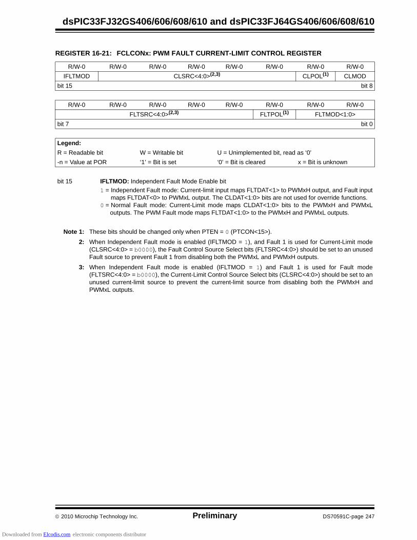
2010 Microchip Technology Inc. Preliminary DS70591C-page 247
dsPIC33FJ32GS406/606/608/610 and dsPIC33FJ64GS406/606/608/610
REGISTER 16-21: FCLCONx: PWM FAULT CURRENT-LIMIT CONTROL REGISTER
R/W-0 R/W-0 R/W-0 R/W-0 R/W-0 R/W-0 R/W-0 R/W-0
IFLTMOD CLSRC<4:0>(2,3) CLPOL(1) CLMOD
bit 15 bit 8
R/W-0 R/W-0 R/W-0 R/W-0 R/W-0 R/W-0 R/W-0 R/W-0
FLTSRC<4:0>(2,3) FLTPOL(1) FLTMOD<1:0>
bit 7 bit 0
Legend:
R = Readable bit W = Writable bit U = Unimplemented bit, read as ‘0’
-n = Value at POR ‘1’ = Bit is set ‘0’ = Bit is cleared x = Bit is unknown
bit 15 IFLTMOD: Independent Fault Mode Enable bit
1 = Independent Fault mode: Current-limit input maps FLTDAT<1> to PWMxH output, and Fault inputmaps FLTDAT<0> to PWMxL output. The CLDAT<1:0> bits are not used for override functions.
0 = Normal Fault mode: Current-Limit mode maps CLDAT<1:0> bits to the PWMxH and PWMxLoutputs. The PWM Fault mode maps FLTDAT<1:0> to the PWMxH and PWMxL outputs.
Note 1: These bits should be changed only when PTEN = 0 (PTCON<15>).
2: When Independent Fault mode is enabled (IFLTMOD = 1), and Fault 1 is used for Current-Limit mode(CLSRC<4:0> = b0000), the Fault Control Source Select bits (FLTSRC<4:0>) should be set to an unusedFault source to prevent Fault 1 from disabling both the PWMxL and PWMxH outputs.
3: When Independent Fault mode is enabled (IFLTMOD = 1) and Fault 1 is used for Fault mode(FLTSRC<4:0> = b0000), the Current-Limit Control Source Select bits (CLSRC<4:0>) should be set to anunused current-limit source to prevent the current-limit source from disabling both the PWMxH andPWMxL outputs.
Downloaded from Elcodis.com electronic components distributor

dsPIC33FJ32GS406/606/608/610 and dsPIC33FJ64GS406/606/608/610
DS70591C-page 248 Preliminary 2010 Microchip Technology Inc.
bit 14-10 CLSRC<4:0>: Current-Limit Control Signal Source Select bits for PWM Generator #(2,4). These bits also specify the source for the dead time compensation input signal, DTCMPx.
11111 = Reserved11110 = Fault 2311101 = Fault 2211100 = Fault 2111011 = Fault 2011010 = Fault 1911001 = Fault 1811000 = Fault 1710111 = Fault 1610110 = Fault 1510101 = Fault 1410100 = Fault 1310011 = Fault 1210010 = Fault 1110001 = Fault 1010000 = Fault 901111 = Fault 801110 = Fault 701101 = Fault 601100 = Fault 501011 = Fault 401010 = Fault 301001 = Fault 201000 = Fault 100111 = Reserved00110 = Reserved00101 = Reserved00100 = Reserved00011 = Analog Comparator 400010 = Analog Comparator 300001 = Analog Comparator 200000 = Analog Comparator 1
bit 9 CLPOL: Current-Limit Polarity bit for PWM Generator #(1)
1 = The selected current-limit source is active-low0 = The selected current-limit source is active-high
bit 8 CLMOD: Current-Limit Mode Enable bit for PWM Generator #
1 = Current-Limit mode is enabled0 = Current-Limit mode is disabled
REGISTER 16-21: FCLCONx: PWM FAULT CURRENT-LIMIT CONTROL REGISTER (CONTINUED)
Note 1: These bits should be changed only when PTEN = 0 (PTCON<15>).
2: When Independent Fault mode is enabled (IFLTMOD = 1), and Fault 1 is used for Current-Limit mode(CLSRC<4:0> = b0000), the Fault Control Source Select bits (FLTSRC<4:0>) should be set to an unusedFault source to prevent Fault 1 from disabling both the PWMxL and PWMxH outputs.
3: When Independent Fault mode is enabled (IFLTMOD = 1) and Fault 1 is used for Fault mode(FLTSRC<4:0> = b0000), the Current-Limit Control Source Select bits (CLSRC<4:0>) should be set to anunused current-limit source to prevent the current-limit source from disabling both the PWMxH andPWMxL outputs.
Downloaded from Elcodis.com electronic components distributor

2010 Microchip Technology Inc. Preliminary DS70591C-page 249
dsPIC33FJ32GS406/606/608/610 and dsPIC33FJ64GS406/606/608/610
bit 7-3 FLTSRC<4:0>: Fault Control Signal Source Select bits for PWM Generator #(2,4)
11111 = Reserved11110 = Fault 2311101 = Fault 2211100 = Fault 2111011 = Fault 2011010 = Fault 1911001 = Fault 1811000 = Fault 1710111 = Fault 1610110 = Fault 1510101 = Fault 1410100 = Fault 1310011 = Fault 1210010 = Fault 1110001 = Fault 1010000 = Fault 901111 = Fault 801110 = Fault 701101 = Fault 601100 = Fault 501011 = Fault 401010 = Fault 301001 = Fault 201000 = Fault 100111 = Reserved00110 = Reserved00101 = Reserved00100 = Reserved00011 = Analog Comparator 400010 = Analog Comparator 300001 = Analog Comparator 200000 = Analog Comparator 1
bit 2 FLTPOL: Fault Polarity bit for PWM Generator #(1)
1 = The selected Fault source is active-low0 = The selected Fault source is active-high
bit 1-0 FLTMOD<1:0>: Fault Mode bits for PWM Generator #
11 = Fault input is disabled10 = Reserved01 = The selected Fault source forces PWMxH, PWMxL pins to FLTDAT values (cycle)00 = The selected Fault source forces PWMxH, PWMxL pins to FLTDAT values (latched condition)
REGISTER 16-21: FCLCONx: PWM FAULT CURRENT-LIMIT CONTROL REGISTER (CONTINUED)
Note 1: These bits should be changed only when PTEN = 0 (PTCON<15>).
2: When Independent Fault mode is enabled (IFLTMOD = 1), and Fault 1 is used for Current-Limit mode(CLSRC<4:0> = b0000), the Fault Control Source Select bits (FLTSRC<4:0>) should be set to an unusedFault source to prevent Fault 1 from disabling both the PWMxL and PWMxH outputs.
3: When Independent Fault mode is enabled (IFLTMOD = 1) and Fault 1 is used for Fault mode(FLTSRC<4:0> = b0000), the Current-Limit Control Source Select bits (CLSRC<4:0>) should be set to anunused current-limit source to prevent the current-limit source from disabling both the PWMxH andPWMxL outputs.
Downloaded from Elcodis.com electronic components distributor
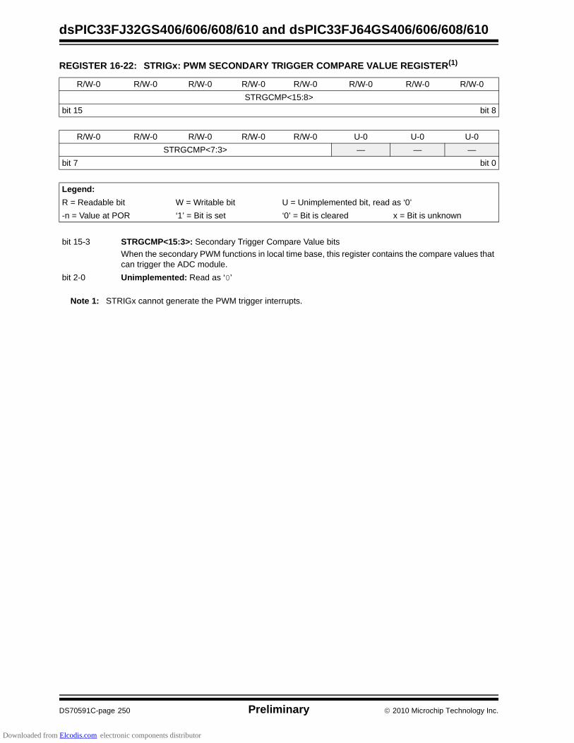
dsPIC33FJ32GS406/606/608/610 and dsPIC33FJ64GS406/606/608/610
DS70591C-page 250 Preliminary 2010 Microchip Technology Inc.
REGISTER 16-22: STRIGx: PWM SECONDARY TRIGGER COMPARE VALUE REGISTER(1)
R/W-0 R/W-0 R/W-0 R/W-0 R/W-0 R/W-0 R/W-0 R/W-0
STRGCMP<15:8>
bit 15 bit 8
R/W-0 R/W-0 R/W-0 R/W-0 R/W-0 U-0 U-0 U-0
STRGCMP<7:3> — — —
bit 7 bit 0
Legend:
R = Readable bit W = Writable bit U = Unimplemented bit, read as ‘0’
-n = Value at POR ‘1’ = Bit is set ‘0’ = Bit is cleared x = Bit is unknown
bit 15-3 STRGCMP<15:3>: Secondary Trigger Compare Value bits
When the secondary PWM functions in local time base, this register contains the compare values that can trigger the ADC module.
bit 2-0 Unimplemented: Read as ‘0’
Note 1: STRIGx cannot generate the PWM trigger interrupts.
Downloaded from Elcodis.com electronic components distributor

2010 Microchip Technology Inc. Preliminary DS70591C-page 251
dsPIC33FJ32GS406/606/608/610 and dsPIC33FJ64GS406/606/608/610
REGISTER 16-23: LEBCONx: LEADING-EDGE BLANKING CONTROL REGISTER
R/W-0 R/W-0 R/W-0 R/W-0 R/W-0 R/W-0 U-0 U-0
PHR PHF PLR PLF FLTLEBEN CLLEBEN — —
bit 15 bit 8
U-0 U-0 R/W-0 R/W-0 R/W-0 R/W-0 R/W-0 R/W-0
— — BCH BCL BPHH BPHL BPLH BPLL
bit 7 bit 0
Legend:
R = Readable bit W = Writable bit U = Unimplemented bit, read as ‘0’
-n = Value at POR ‘1’ = Bit is set ‘0’ = Bit is cleared x = Bit is unknown
bit 15 PHR: PWMxH Rising Edge Trigger Enable bit1 = Rising edge of PWMxH will trigger Leading-Edge Blanking counter0 = Leading-Edge Blanking ignores rising edge of PWMxH
bit 14 PHF: PWMxH Falling Edge Trigger Enable bit1 = Falling edge of PWMxH will trigger Leading-Edge Blanking counter0 = Leading-Edge Blanking ignores falling edge of PWMxH
bit 13 PLR: PWMxL Rising Edge Trigger Enable bit1 = Rising edge of PWMxL will trigger Leading-Edge Blanking counter0 = Leading-Edge Blanking ignores rising edge of PWMxL
bit 12 PLF: PWMxL Falling Edge Trigger Enable bit1 = Falling edge of PWMxL will trigger Leading-Edge Blanking counter0 = Leading-Edge Blanking ignores falling edge of PWMxL
bit 11 FLTLEBEN: Fault Input Leading-Edge Blanking Enable bit1 = Leading-Edge Blanking is applied to selected fault input0 = Leading-Edge Blanking is not applied to selected fault input
bit 10 CLLEBEN: Current-Limit Leading-Edge Blanking Enable bit1 = Leading-Edge Blanking is applied to selected current-limit input0 = Leading-Edge Blanking is not applied to selected current-limit input
bit 9-6 Unimplemented: Read as ‘0’
bit 5 BCH: Blanking in Selected-Blanking Signal High Enable bit(1)
1 = State blanking (of current-limit and/or fault input signals) when selected blanking signal is high0 = No blanking when selected blanking signal is high
bit 4 BCL: Blanking in Selected-Blanking Signal Low Enable bit(1)
1 = State blanking (of current-limit and/or fault input signals) when selected blanking signal is low0 = No blanking when selected blanking signal is low
bit 3 BPHH: Blanking in PWMxH High Enable bit
1 = State blanking (of current-limit and/or fault input signals) when PWMxH output is high0 = No blanking when PWMxH output is high
bit 2 BPHL: Blanking in PWMxH Low Enable bit
1 = State blanking (of current-limit and/or fault input signals) when PWMxH output is low0 = No blanking when PWMxH output is low
bit 1 BPLH: Blanking in PWMxL High Enable bit
1 = State blanking (of current-limit and/or fault input signals) when PWMxL output is high0 = No blanking when PWMxL output is high
bit 0 BPLL: Blanking in PWMxL Low Enable bit
1 = State blanking (of current-limit and/or fault input signals) when PWMxL output is low0 = No blanking when PWMxL output is low
Note 1: The blanking signal is selected via the BLANKSEL bits in the AUXCONx register.
Downloaded from Elcodis.com electronic components distributor

dsPIC33FJ32GS406/606/608/610 and dsPIC33FJ64GS406/606/608/610
DS70591C-page 252 Preliminary 2010 Microchip Technology Inc.
REGISTER 16-24: LEBDLYx: LEADING-EDGE BLANKING DELAY REGISTER
U-0 U-0 U-0 U-0 R/W-0 R/W-0 R/W-0 R/W-0
— — — — LEB<11:8>
bit 15 bit 8
R/W-0 R/W-0 R/W-0 R/W-0 R/W-0 U-0 U-0 U-0
LEB<7:3> — — —
bit 7 bit 0
Legend:
R = Readable bit W = Writable bit U = Unimplemented bit, read as ‘0’
-n = Value at POR ‘1’ = Bit is set ‘0’ = Bit is cleared x = Bit is unknown
bit 15-12 Unimplemented: Read as ‘0’
bit 11-3 LEB<11:3>: Leading-Edge Blanking Delay bits for Current-Limit and Fault Inputs
Value in 8.32 ns increments
bit 2-0 Unimplemented: Read as ‘0’
Note: The LEB delay timing operates with the primary PWM clock prescaler bits, PCLKDIV<2:0>(PTCON<10:8>).
Downloaded from Elcodis.com electronic components distributor

2010 Microchip Technology Inc. Preliminary DS70591C-page 253
dsPIC33FJ32GS406/606/608/610 and dsPIC33FJ64GS406/606/608/610
REGISTER 16-25: AUXCONx: PWM AUXILIARY CONTROL REGISTER
R/W-0 R/W-0 U-0 U-0 R/W-0 R/W-0 R/W-0 R/W-0
HRPDIS HRDDIS — — BLANKSEL<3:0>
bit 15 bit 8
U-0 U-0 R/W-0 R/W-0 R/W-0 R/W-0 R/W-0 R/W-0
— — CHOPSEL<3:0> CHOPHEN CHOPLEN
bit 7 bit 0
Legend:
R = Readable bit W = Writable bit U = Unimplemented bit, read as ‘0’
-n = Value at POR ‘1’ = Bit is set ‘0’ = Bit is cleared x = Bit is unknown
bit 15 HRPDIS: High Resolution PWM Period Disable bit(1)
1 = High resolution PWM period is disabled to reduce power consumption0 = High resolution PWM period is enabled
bit 14 HRDDIS: High Resolution PWM Duty Cycle Disable bit(1)
1 = High resolution PWM duty cycle is disabled to reduce power consumption0 = High resolution PWM duty cycle is enabled
bit 13-12 Unimplemented: Read as ‘0’
bit 11-8 BLANKSEL<3:0>: PWM State Blank Source Select bitsThe selected state blank signal will block the current limit and/or fault input signals (if enabled via the BCH and BCL bits in the LEBCONx register)1001 = PWM9H selected as state blank source1000 = PWM8H selected as state blank source0111 = PWM7H selected as state blank source0110 = PWM6H selected as state blank source0101 = PWM5H selected as state blank source0100 = PWM4H selected as state blank source0011 = PWM3H selected as state blank source0010 = PWM2H selected as state blank source0001 = PWM1H selected as state blank source0000 = 1’b0 (no state blanking)
bit 7-6 Unimplemented: Read as ‘0’
bit 5-2 CHOPSEL<3:0>: PWM Chop Clock Source Select bitsThe selected signal will enable and disable (CHOP) the selected PWM outputs1001 = PWM9H selected as CHOP clock source1000 = PWM8H selected as CHOP clock source0111 = PWM7H selected as CHOP clock source0110 = PWM6H selected as CHOP clock source0101 = PWM5H selected as CHOP clock source0100 = PWM4H selected as CHOP clock source0011 = PWM3H selected as CHOP clock source0010 = PWM2H selected as CHOP clock source0001 = PWM1H selected as CHOP clock source0000 = Chop Clock generator selected as CHOP clock source
bit 1 CHOPHEN: PWMxH Output Chopping Enable bit1 = PWMxH chopping function is enabled0 = PWMxH chopping function is disabled
bit 0 CHOPLEN: PWMxL Output Chopping Enable bit1 = PWMxL chopping function is enabled0 = PWMxL chopping function is disabled
Downloaded from Elcodis.com electronic components distributor

dsPIC33FJ32GS406/606/608/610 and dsPIC33FJ64GS406/606/608/610
DS70591C-page 254 Preliminary 2010 Microchip Technology Inc.
REGISTER 16-26: PWMCAPx: PRIMARY PWM TIME BASE CAPTURE REGISTER
R-0 R-0 R-0 R-0 R-0 R-0 R-0 R-0
PWMCAP<15:8>
bit 15 bit 8
R-0 R-0 R-0 R-0 R-0 U-0 U-0 U-0
PWMCAP<7:3> — — —
bit 7 bit 0
Legend:
R = Readable bit W = Writable bit U = Unimplemented bit, read as ‘0’
-n = Value at POR ‘1’ = Bit is set ‘0’ = Bit is cleared x = Bit is unknown
bit 15-3 PWMCAP<15:3>: Captured PWM Time Base Value bits(1,2,3,4)
The value in this register represents the captured PWM time base value when a leading edge isdetected on the current-limit input.
bit 2-0 Unimplemented: Read as ‘0’
Note 1: The capture feature is only available on primary output (PWMxH).
2: This feature is active only after LEB processing on the current-limit input signal is complete.
3: The minimum capture resolution is 8.32 ns.
4: This feature can be used when the XPRES bit (PWMCONx<1>) is set to ‘0’.
Downloaded from Elcodis.com electronic components distributor

2010 Microchip Technology Inc. Preliminary DS70591C-page 255
dsPIC33FJ32GS406/606/608/610 and dsPIC33FJ64GS406/606/608/610
17.0 QUADRATURE ENCODER INTERFACE (QEI) MODULE
This chapter describes the Quadrature Encoder Inter-face (QEI) module and associated operational modes.The QEI module provides the interface to incrementalencoders for obtaining mechanical position data.
The operational features of the QEI include:
• Three input channels for two phase signals and index pulse
• 16-bit up/down position counter• Count direction status
• Position Measurement (x2 and x4) mode• Programmable digital noise filters on inputs• Alternate 16-bit Timer/Counter mode• Quadrature Encoder Interface interrupts
These operating modes are determined by setting theappropriate bits, QEIM<2:0> in (QEIxCON<10:8>).Figure 17-1 depicts the Quadrature Encoder Interfaceblock diagram.
FIGURE 17-1: QUADRATURE ENCODER INTERFACE BLOCK DIAGRAM (x = 1 OR 2)
Note 1: This data sheet summarizes the featuresof the dsPIC33FJ32GS406/606/608/610and dsPIC33FJ64GS406/606/608/610families of devices. It is not intended to bea comprehensive reference source. Tocomplement the information in this datasheet, refer to Section 15. “QuadratureEncoder Interface (QEI)” (DS70208) inthe “dsPIC33F/PIC24H Family ReferenceManual”, which is available from theMicrochip web site (www.microchip.com).
2: Some registers and associated bitsdescribed in this section may not be avail-able on all devices. Refer to Section 4.0“Memory Organization” in this datasheet for device-specific register and bitinformation. Note: An ‘x’ used in the names of pins, control/
status bits and registers denotes aparticular Quadrature Encoder Interface(QEI) module number (x = 1 or 2).
16-bit Up/Down Counter
Comparator/
Max Count Register
QEAx(1)
INDXx(1)
0
1Up/Down
Existing Pin Logic
UPDNx
3
QEBx(1)
QEIM<2:0>Mode Select
3
(POSxCNT)
(MAXxCNT)
PCDOUT
QExIFEvent Flag
Reset
Equal
2
TCY
1
0
TQCSTQCKPS<1:0>
2
Q
QD
CK
TQGATE
QEIM<2:0>
1
0
Sleep Input
0
1
UPDN_SRC
QEIxCON<11>Zero Detect
Synchronize
Det 1, 8, 64, 256Prescaler
QuadratureEncoder
Interface Logic
Programmable
Digital Filter
Programmable
Digital Filter
Programmable
Digital Filter
Note 1: The QEI1 module can be connected to the QEA1/QEB1/INDX1or AQEA1/AQEB1/AINDX1 pins, which are controlled by clearingor setting the ALTQIO bit in the FPOR Configuration register. SeeSection 24.0 “Special Features” for more information.
Downloaded from Elcodis.com electronic components distributor
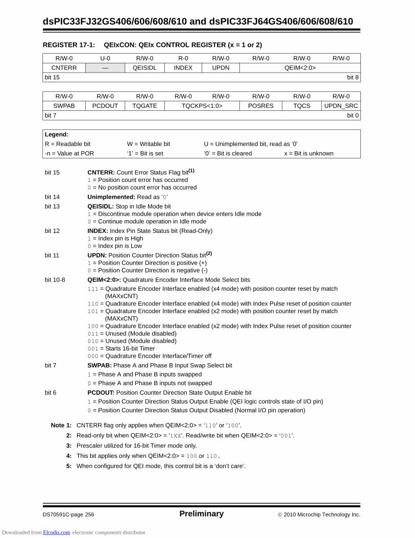
dsPIC33FJ32GS406/606/608/610 and dsPIC33FJ64GS406/606/608/610
DS70591C-page 256 Preliminary 2010 Microchip Technology Inc.
REGISTER 17-1: QEIxCON: QEIx CONTROL REGISTER (x = 1 or 2)
R/W-0 U-0 R/W-0 R-0 R/W-0 R/W-0 R/W-0 R/W-0
CNTERR — QEISIDL INDEX UPDN QEIM<2:0>
bit 15 bit 8
R/W-0 R/W-0 R/W-0 R/W-0 R/W-0 R/W-0 R/W-0 R/W-0
SWPAB PCDOUT TQGATE TQCKPS<1:0> POSRES TQCS UPDN_SRC
bit 7 bit 0
Legend:
R = Readable bit W = Writable bit U = Unimplemented bit, read as ‘0’
-n = Value at POR ‘1’ = Bit is set ‘0’ = Bit is cleared x = Bit is unknown
bit 15 CNTERR: Count Error Status Flag bit(1)
1 = Position count error has occurred0 = No position count error has occurred
bit 14 Unimplemented: Read as ‘0’
bit 13 QEISIDL: Stop in Idle Mode bit1 = Discontinue module operation when device enters Idle mode0 = Continue module operation in Idle mode
bit 12 INDEX: Index Pin State Status bit (Read-Only)1 = Index pin is High0 = Index pin is Low
bit 11 UPDN: Position Counter Direction Status bit(2)
1 = Position Counter Direction is positive (+)0 = Position Counter Direction is negative (-)
bit 10-8 QEIM<2:0>: Quadrature Encoder Interface Mode Select bits
111 = Quadrature Encoder Interface enabled (x4 mode) with position counter reset by match(MAXxCNT)
110 = Quadrature Encoder Interface enabled (x4 mode) with Index Pulse reset of position counter101 = Quadrature Encoder Interface enabled (x2 mode) with position counter reset by match
(MAXxCNT)100 = Quadrature Encoder Interface enabled (x2 mode) with Index Pulse reset of position counter011 = Unused (Module disabled)010 = Unused (Module disabled)001 = Starts 16-bit Timer000 = Quadrature Encoder Interface/Timer off
bit 7 SWPAB: Phase A and Phase B Input Swap Select bit
1 = Phase A and Phase B inputs swapped
0 = Phase A and Phase B inputs not swapped
bit 6 PCDOUT: Position Counter Direction State Output Enable bit
1 = Position Counter Direction Status Output Enable (QEI logic controls state of I/O pin)
0 = Position Counter Direction Status Output Disabled (Normal I/O pin operation)
Note 1: CNTERR flag only applies when QEIM<2:0> = ‘110’ or ‘100’.
2: Read-only bit when QEIM<2:0> = ‘1XX’. Read/write bit when QEIM<2:0> = ‘001’.
3: Prescaler utilized for 16-bit Timer mode only.
4: This bit applies only when QEIM<2:0> = 100 or 110.
5: When configured for QEI mode, this control bit is a ‘don’t care’.
Downloaded from Elcodis.com electronic components distributor
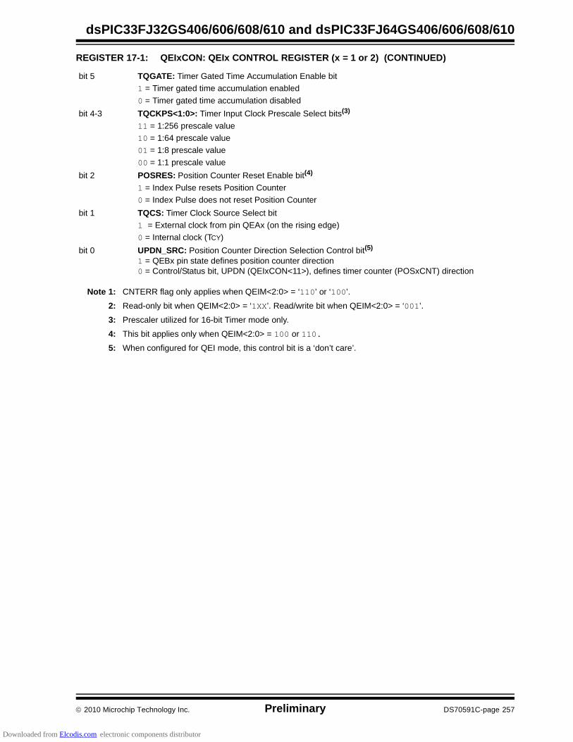
2010 Microchip Technology Inc. Preliminary DS70591C-page 257
dsPIC33FJ32GS406/606/608/610 and dsPIC33FJ64GS406/606/608/610
bit 5 TQGATE: Timer Gated Time Accumulation Enable bit
1 = Timer gated time accumulation enabled
0 = Timer gated time accumulation disabled
bit 4-3 TQCKPS<1:0>: Timer Input Clock Prescale Select bits(3)
11 = 1:256 prescale value
10 = 1:64 prescale value
01 = 1:8 prescale value
00 = 1:1 prescale value
bit 2 POSRES: Position Counter Reset Enable bit(4)
1 = Index Pulse resets Position Counter
0 = Index Pulse does not reset Position Counter
bit 1 TQCS: Timer Clock Source Select bit
1 = External clock from pin QEAx (on the rising edge)
0 = Internal clock (TCY)
bit 0 UPDN_SRC: Position Counter Direction Selection Control bit(5)
1 = QEBx pin state defines position counter direction0 = Control/Status bit, UPDN (QEIxCON<11>), defines timer counter (POSxCNT) direction
REGISTER 17-1: QEIxCON: QEIx CONTROL REGISTER (x = 1 or 2) (CONTINUED)
Note 1: CNTERR flag only applies when QEIM<2:0> = ‘110’ or ‘100’.
2: Read-only bit when QEIM<2:0> = ‘1XX’. Read/write bit when QEIM<2:0> = ‘001’.
3: Prescaler utilized for 16-bit Timer mode only.
4: This bit applies only when QEIM<2:0> = 100 or 110.
5: When configured for QEI mode, this control bit is a ‘don’t care’.
Downloaded from Elcodis.com electronic components distributor
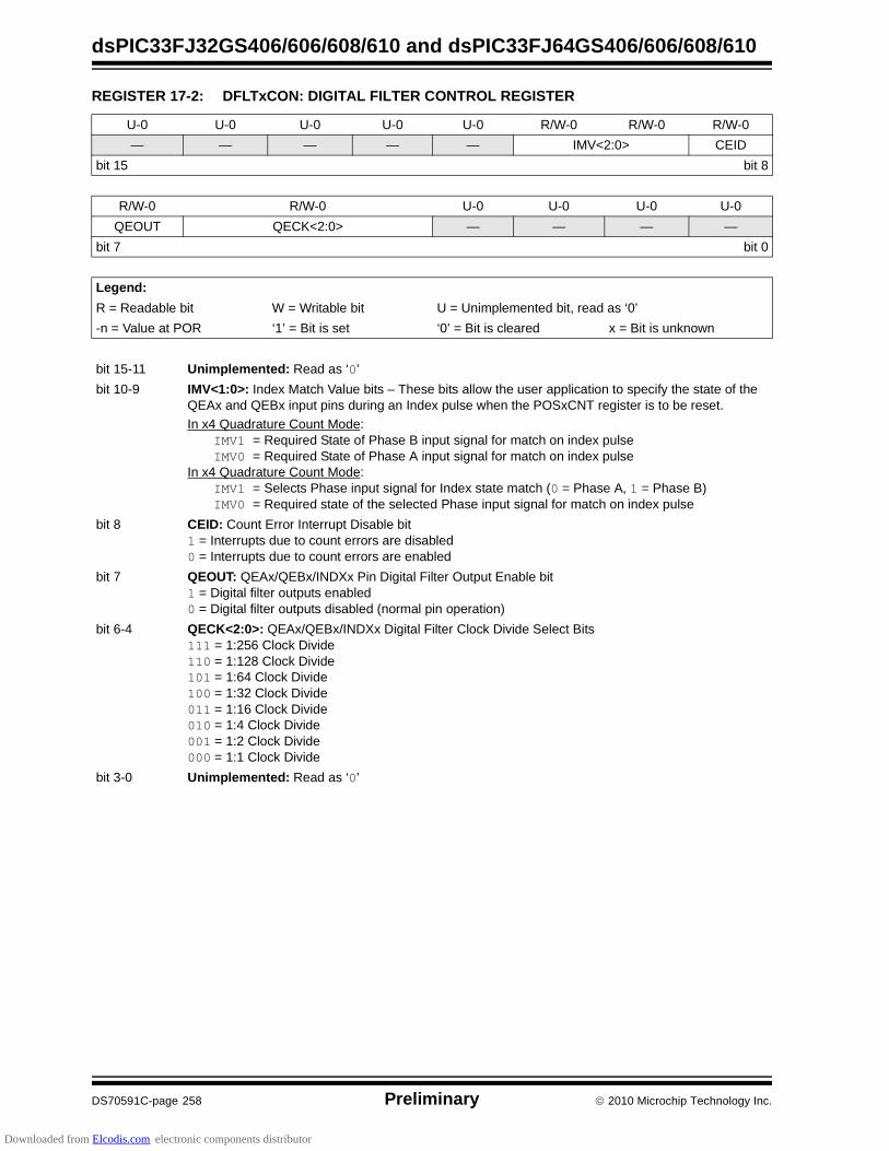
dsPIC33FJ32GS406/606/608/610 and dsPIC33FJ64GS406/606/608/610
DS70591C-page 258 Preliminary 2010 Microchip Technology Inc.
REGISTER 17-2: DFLTxCON: DIGITAL FILTER CONTROL REGISTER
U-0 U-0 U-0 U-0 U-0 R/W-0 R/W-0 R/W-0
— — — — — IMV<2:0> CEID
bit 15 bit 8
R/W-0 R/W-0 U-0 U-0 U-0 U-0
QEOUT QECK<2:0> — — — —
bit 7 bit 0
Legend:
R = Readable bit W = Writable bit U = Unimplemented bit, read as ‘0’
-n = Value at POR ‘1’ = Bit is set ‘0’ = Bit is cleared x = Bit is unknown
bit 15-11 Unimplemented: Read as ‘0’
bit 10-9 IMV<1:0>: Index Match Value bits – These bits allow the user application to specify the state of the QEAx and QEBx input pins during an Index pulse when the POSxCNT register is to be reset.
In x4 Quadrature Count Mode:IMV1 = Required State of Phase B input signal for match on index pulseIMV0 = Required State of Phase A input signal for match on index pulse
In x4 Quadrature Count Mode:IMV1 = Selects Phase input signal for Index state match (0 = Phase A, 1 = Phase B)IMV0 = Required state of the selected Phase input signal for match on index pulse
bit 8 CEID: Count Error Interrupt Disable bit1 = Interrupts due to count errors are disabled0 = Interrupts due to count errors are enabled
bit 7 QEOUT: QEAx/QEBx/INDXx Pin Digital Filter Output Enable bit1 = Digital filter outputs enabled0 = Digital filter outputs disabled (normal pin operation)
bit 6-4 QECK<2:0>: QEAx/QEBx/INDXx Digital Filter Clock Divide Select Bits111 = 1:256 Clock Divide110 = 1:128 Clock Divide101 = 1:64 Clock Divide100 = 1:32 Clock Divide011 = 1:16 Clock Divide010 = 1:4 Clock Divide001 = 1:2 Clock Divide000 = 1:1 Clock Divide
bit 3-0 Unimplemented: Read as ‘0’
Downloaded from Elcodis.com electronic components distributor

2010 Microchip Technology Inc. Preliminary DS70591C-page 259
dsPIC33FJ32GS406/606/608/610 and dsPIC33FJ64GS406/606/608/610
18.0 SERIAL PERIPHERAL INTERFACE (SPI)
The Serial Peripheral Interface (SPI) module is asynchronous serial interface useful for communicatingwith other peripheral or microcontroller devices. Theseperipheral devices can be serial EEPROMs, shiftregisters, display drivers, analog-to-digital convertersand so on. The SPI module is compatible with SPI andSIOP from Motorola®.
The SPI module consists of a 16-bit shift register,SPIxSR (where x = 1), used for shifting data in and out,and a buffer register, SPIxBUF. A control register,SPIxCON, configures the module. Additionally, aSTATUS register, SPIxSTAT, indicates statusconditions.
The serial interface consists of 4 pins:
• SDIx (Serial Data Input)• SDOx (Serial Data Output)• SCKx (Shift Clock Input Or Output)• SSx (Active-Low Slave Select).
In Master mode operation, SCK is a clock output; inSlave mode, it is a clock input.
FIGURE 18-1: SPI MODULE BLOCK DIAGRAM
Note 1: This data sheet summarizes the featuresof the dsPIC33FJ32GS406/606/608/610and dsPIC33FJ64GS406/606/608/610families of devices. It is not intended to bea comprehensive reference source. Tocomplement the information in this datasheet, refer to Section 18. “SerialPeripheral Interface (SPI)” (DS70206)in the “dsPIC33F/PIC24H Family Refer-ence Manual”, which is available from theMicrochip web site (www.microchip.com).
2: Some registers and associated bitsdescribed in this section may not be avail-able on all devices. Refer to Section 4.0“Memory Organization” in this datasheet for device-specific register and bitinformation.
Internal Data Bus
SDIx
SDOx
SSx(1)
SCKx
SPIxSR
bit 0
Shift Control
EdgeSelect
FCYPrimary1:1/4/16/64
Enable
Prescaler
Sync
SPIxBUF
Control
TransferTransfer
Write SPIxBUFRead SPIxBUF
16
SPIxCON1<1:0>
SPIxCON1<4:2>
Master Clock
ClockControl
SecondaryPrescaler
1:1 to 1:8
SPIxRXB SPIxTXB
Note 1: The SPI1 module can be connected to the SS1 or ASS1 pins, which are controlled by clearing or setting theALTSS1 bit in the FPOR Configuration register. See Section 24.0 “Special Features” for more information.
Downloaded from Elcodis.com electronic components distributor

dsPIC33FJ32GS406/606/608/610 and dsPIC33FJ64GS406/606/608/610
DS70591C-page 260 Preliminary 2010 Microchip Technology Inc.
REGISTER 18-1: SPIxSTAT: SPIx STATUS AND CONTROL REGISTER
R/W-0 U-0 R/W-0 U-0 U-0 U-0 U-0 U-0
SPIEN — SPISIDL — — — — —
bit 15 bit 8
U-0 R/C-0 U-0 U-0 U-0 U-0 R-0 R-0
— SPIROV — — — — SPITBF SPIRBF
bit 7 bit 0
Legend: C = Clearable bit
R = Readable bit W = Writable bit U = Unimplemented bit, read as ‘0’
-n = Value at POR ‘1’ = Bit is set ‘0’ = Bit is cleared x = Bit is unknown
bit 15 SPIEN: SPIx Enable bit
1 = Enables module and configures SCKx, SDOx, SDIx and SSx as serial port pins0 = Disables module
bit 14 Unimplemented: Read as ‘0’
bit 13 SPISIDL: Stop in Idle Mode bit
1 = Discontinue module operation when device enters Idle mode0 = Continue module operation in Idle mode
bit 12-7 Unimplemented: Read as ‘0’
bit 6 SPIROV: Receive Overflow Flag bit1 = A new byte/word is completely received and discarded. The user software has not read the
previous data in the SPIxBUF register.0 = No overflow has occurred
bit 5-2 Unimplemented: Read as ‘0’
bit 1 SPITBF: SPIx Transmit Buffer Full Status bit
1 = Transmit not yet started, SPIxTXB is full0 = Transmit started, SPIxTXB is empty. Automatically set in hardware when CPU writes SPIxBUF
location, loading SPIxTXB. Automatically cleared in hardware when SPIx module transfers datafrom SPIxTXB to SPIxSR.
bit 0 SPIRBF: SPIx Receive Buffer Full Status bit
1 = Receive complete, SPIxRXB is full0 = Receive is not complete, SPIxRXB is empty. Automatically set in hardware when SPIx transfers
data from SPIxSR to SPIxRXB. Automatically cleared in hardware when core reads SPIxBUFlocation, reading SPIxRXB.
Downloaded from Elcodis.com electronic components distributor

2010 Microchip Technology Inc. Preliminary DS70591C-page 261
dsPIC33FJ32GS406/606/608/610 and dsPIC33FJ64GS406/606/608/610
REGISTER 18-2: SPIXCON1: SPIx CONTROL REGISTER 1
U-0 U-0 U-0 R/W-0 R/W-0 R/W-0 R/W-0 R/W-0
— — — DISSCK DISSDO MODE16 SMP CKE(1)
bit 15 bit 8
R/W-0 R/W-0 R/W-0 R/W-0 R/W-0 R/W-0 R/W-0 R/W-0
SSEN(3) CKP MSTEN SPRE<2:0>(2) PPRE<1:0>(2)
bit 7 bit 0
Legend:
R = Readable bit W = Writable bit U = Unimplemented bit, read as ‘0’
-n = Value at POR ‘1’ = Bit is set ‘0’ = Bit is cleared x = Bit is unknown
bit 15-13 Unimplemented: Read as ‘0’
bit 12 DISSCK: Disable SCKx pin bit (SPI Master modes only)1 = Internal SPI clock is disabled; pin functions as I/O0 = Internal SPI clock is enabled
bit 11 DISSDO: Disable SDOx pin bit1 = SDOx pin is not used by module; pin functions as I/O0 = SDOx pin is controlled by the module
bit 10 MODE16: Word/Byte Communication Select bit1 = Communication is word-wide (16 bits)0 = Communication is byte-wide (8 bits)
bit 9 SMP: SPIx Data Input Sample Phase bitMaster mode:1 = Input data sampled at end of data output time0 = Input data sampled at middle of data output timeSlave mode:SMP must be cleared when SPIx is used in Slave mode.
bit 8 CKE: SPIx Clock Edge Select bit(1)
1 = Serial output data changes on transition from active clock state to Idle clock state (see bit 6)0 = Serial output data changes on transition from Idle clock state to active clock state (see bit 6)
bit 7 SSEN: Slave Select Enable bit (Slave mode)(3)
1 = SSx pin used for Slave mode0 = SSx pin not used by module; pin controlled by port function
bit 6 CKP: Clock Polarity Select bit1 = Idle state for clock is a high level; active state is a low level0 = Idle state for clock is a low level; active state is a high level
bit 5 MSTEN: Master Mode Enable bit1 = Master mode0 = Slave mode
Note 1: The CKE bit is not used in the Framed SPI modes. Program this bit to ‘0’ for the Framed SPI modes(FRMEN = 1).
2: Do not set both primary and secondary prescalers to a value of 1:1.
3: This bit must be cleared when FRMEN = 1.
Downloaded from Elcodis.com electronic components distributor
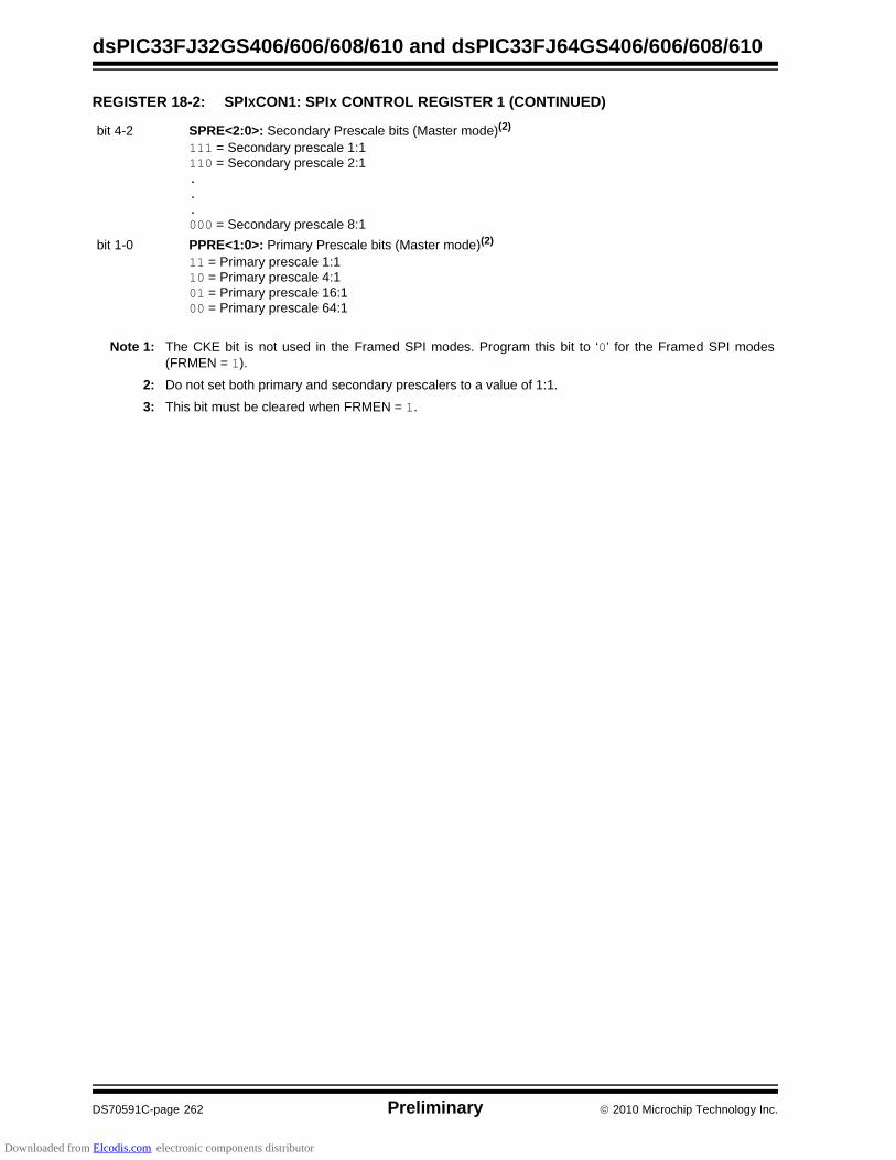
dsPIC33FJ32GS406/606/608/610 and dsPIC33FJ64GS406/606/608/610
DS70591C-page 262 Preliminary 2010 Microchip Technology Inc.
bit 4-2 SPRE<2:0>: Secondary Prescale bits (Master mode)(2)
111 = Secondary prescale 1:1110 = Secondary prescale 2:1...000 = Secondary prescale 8:1
bit 1-0 PPRE<1:0>: Primary Prescale bits (Master mode)(2)
11 = Primary prescale 1:110 = Primary prescale 4:101 = Primary prescale 16:100 = Primary prescale 64:1
REGISTER 18-2: SPIXCON1: SPIx CONTROL REGISTER 1 (CONTINUED)
Note 1: The CKE bit is not used in the Framed SPI modes. Program this bit to ‘0’ for the Framed SPI modes(FRMEN = 1).
2: Do not set both primary and secondary prescalers to a value of 1:1.
3: This bit must be cleared when FRMEN = 1.
Downloaded from Elcodis.com electronic components distributor

2010 Microchip Technology Inc. Preliminary DS70591C-page 263
dsPIC33FJ32GS406/606/608/610 and dsPIC33FJ64GS406/606/608/610
REGISTER 18-3: SPIxCON2: SPIx CONTROL REGISTER 2
R/W-0 R/W-0 R/W-0 U-0 U-0 U-0 U-0 U-0
FRMEN SPIFSD FRMPOL — — — — —
bit 15 bit 8
U-0 U-0 U-0 U-0 U-0 U-0 R/W-0 U-0
— — — — — — FRMDLY —
bit 7 bit 0
Legend:
R = Readable bit W = Writable bit U = Unimplemented bit, read as ‘0’
-n = Value at POR ‘1’ = Bit is set ‘0’ = Bit is cleared x = Bit is unknown
bit 15 FRMEN: Framed SPIx Support bit
1 = Framed SPIx support enabled (SSx pin used as frame sync pulse input/output)0 = Framed SPIx support disabled
bit 14 SPIFSD: Frame Sync Pulse Direction Control bit
1 = Frame sync pulse input (slave)0 = Frame sync pulse output (master)
bit 13 FRMPOL: Frame Sync Pulse Polarity bit
1 = Frame sync pulse is active-high0 = Frame sync pulse is active-low
bit 12-2 Unimplemented: Read as ‘0’
bit 1 FRMDLY: Frame Sync Pulse Edge Select bit
1 = Frame sync pulse coincides with first bit clock0 = Frame sync pulse precedes first bit clock
bit 0 Unimplemented: This bit must not be set to ‘1’ by the user application
Downloaded from Elcodis.com electronic components distributor

dsPIC33FJ32GS406/606/608/610 and dsPIC33FJ64GS406/606/608/610
DS70591C-page 264 Preliminary 2010 Microchip Technology Inc.
NOTES:
Downloaded from Elcodis.com electronic components distributor

2010 Microchip Technology Inc. Preliminary DS70591C-page 265
dsPIC33FJ32GS406/606/608/610 and dsPIC33FJ64GS406/606/608/610
19.0 INTER-INTEGRATED CIRCUIT (I2C™)
The Inter-Integrated Circuit (I2C) module providescomplete hardware support for both Slave andMulti-Master modes of the I2C serial communicationstandard with a 16-bit interface.
The I2C module has a 2-pin interface:
• The SCLx pin is clock.• The SDAx pin is data.
The I2C module offers the following key features:
• I2C interface supporting both Master and Slave modes of operation.
• I2C Slave mode supports 7-bit and 10-bit addressing.
• I2C Master mode supports 7-bit and 10-bit addressing.
• I2C port allows bidirectional transfers between master and slaves.
• Serial clock synchronization for I2C port can be used as a handshake mechanism to suspend and resume serial transfer (SCLREL control).
• I2C supports multi-master operation, detects bus collision and arbitrates accordingly.
19.1 Operating Modes
The hardware fully implements all the master and slavefunctions of the I2C Standard and Fast modespecifications, as well as 7-bit and 10-bit addressing.
The I2C module can operate either as a slave or amaster on an I2C bus.
The following types of I2C operation are supported:
• I2C slave operation with 7-bit addressing• I2C slave operation with 10-bit addressing• I2C master operation with 7-bit or 10-bit addressing
For details about the communication sequence in eachof these modes, refer to the “dsPIC33F/PIC24H FamilyReference Manual”. Please see the Microchip web site(www.microchip.com) for the latest “dsPIC33F/PIC24HFamily Reference Manual” sections.
19.2 I2C Registers
I2CxCON and I2CxSTAT are control and STATUSregisters, respectively. The I2CxCON register isreadable and writable. The lower six bits of I2CxSTATare read-only. The remaining bits of the I2CSTAT areread/write:
• I2CxRSR is the shift register used for shifting data internal to the module and the user application has no access to it.
• I2CxRCV is the receive buffer and the register to which data bytes are written, or from which data bytes are read.
• I2CxTRN is the transmit register to which bytes are written during a transmit operation.
• The I2CxADD register holds the slave address.
• A Status bit, ADD10, indicates 10-Bit Address mode.
• The I2CxBRG acts as the Baud Rate Generator (BRG) reload value.
In receive operations, I2CxRSR and I2CxRCV togetherform a double-buffered receiver. When I2CxRSRreceives a complete byte, it is transferred to I2CxRCV,and an interrupt pulse is generated.
Note 1: This data sheet summarizes the featuresof the dsPIC33FJ32GS406/606/608/610and dsPIC33FJ64GS406/606/608/610families of devices. It is not intended to bea comprehensive reference source. Tocomplement the information in this datasheet, refer to Section 19. “Inter-Inte-grated Circuit (I2C™)” (DS70195) in the“dsPIC33F/PIC24H Family ReferenceManual”, which is available from theMicrochip web site (www.microchip.com).
2: Some registers and associated bitsdescribed in this section may not be avail-able on all devices. Refer to Section 4.0“Memory Organization” in this datasheet for device-specific register and bitinformation.
Downloaded from Elcodis.com electronic components distributor
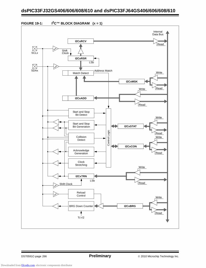
dsPIC33FJ32GS406/606/608/610 and dsPIC33FJ64GS406/606/608/610
DS70591C-page 266 Preliminary 2010 Microchip Technology Inc.
FIGURE 19-1: I2C™ BLOCK DIAGRAM (X = 1)
InternalData Bus
SCLx
SDAx
Shift
Match Detect
I2CxADD
Start and StopBit Detect
Clock
Address Match
ClockStretching
I2CxTRN
LSbShift Clock
BRG Down Counter
ReloadControl
TCY/2
Start and StopBit Generation
AcknowledgeGeneration
CollisionDetect
I2CxCON
I2CxSTAT
Co
ntr
ol L
og
ic
Read
LSb
Write
Read
I2CxBRG
I2CxRSR
Write
Read
Write
Read
Write
Read
Write
Read
Write
Read
I2CxMSK
I2CxRCV
Downloaded from Elcodis.com electronic components distributor

2010 Microchip Technology Inc. Preliminary DS70591C-page 267
dsPIC33FJ32GS406/606/608/610 and dsPIC33FJ64GS406/606/608/610
REGISTER 19-1: I2CxCON: I2Cx CONTROL REGISTER
R/W-0 U-0 R/W-0 R/W-1, HC R/W-0 R/W-0 R/W-0 R/W-0
I2CEN — I2CSIDL SCLREL IPMIEN A10M DISSLW SMEN
bit 15 bit 8
R/W-0 R/W-0 R/W-0 R/W-0, HC R/W-0, HC R/W-0, HC R/W-0, HC R/W-0, HC
GCEN STREN ACKDT ACKEN RCEN PEN RSEN SEN
bit 7 bit 0
Legend: U = Unimplemented bit, read as ‘0’
R = Readable bit W = Writable bit HS = Hardware Settable bit HC = Hardware Clearable bit
-n = Value at POR ‘1’ = Bit is set ‘0’ = Bit is cleared x = Bit is unknown
bit 15 I2CEN: I2Cx Enable bit
1 = Enables the I2Cx module and configures the SDAx and SCLx pins as serial port pins0 = Disables the I2Cx module. All I2C pins are controlled by port functions.
bit 14 Unimplemented: Read as ‘0’
bit 13 I2CSIDL: Stop in Idle Mode bit
1 = Discontinue module operation when device enters an Idle mode0 = Continue module operation in Idle mode
bit 12 SCLREL: SCLx Release Control bit (when operating as I2C slave)
1 = Release SCLx clock0 = Hold SCLx clock low (clock stretch)
If STREN = 1:Bit is R/W (i.e., software can write ‘0’ to initiate stretch and write ‘1’ to release clock). Hardware clearat beginning of slave transmission. Hardware clear at end of slave reception.
If STREN = 0:Bit is R/S (i.e., software can only write ‘1’ to release clock). Hardware clear at beginning of slavetransmission.
bit 11 IPMIEN: Intelligent Peripheral Management Interface (IPMI) Enable bit
1 = IPMI mode is enabled; all addresses Acknowledged0 = IPMI mode disabled
bit 10 A10M: 10-Bit Slave Address bit
1 = I2CxADD is a 10-bit slave address0 = I2CxADD is a 7-bit slave address
bit 9 DISSLW: Disable Slew Rate Control bit
1 = Slew rate control disabled0 = Slew rate control enabled
bit 8 SMEN: SMBus Input Levels bit
1 = Enable I/O pin thresholds compliant with SMBus specification0 = Disable SMBus input thresholds
bit 7 GCEN: General Call Enable bit (when operating as I2C slave)
1 = Enable interrupt when a general call address is received in the I2CxRSR(module is enabled for reception)
0 = General call address disabled
bit 6 STREN: SCLx Clock Stretch Enable bit (when operating as I2C slave)
Used in conjunction with SCLREL bit.1 = Enable software or receive clock stretching0 = Disable software or receive clock stretching
Downloaded from Elcodis.com electronic components distributor
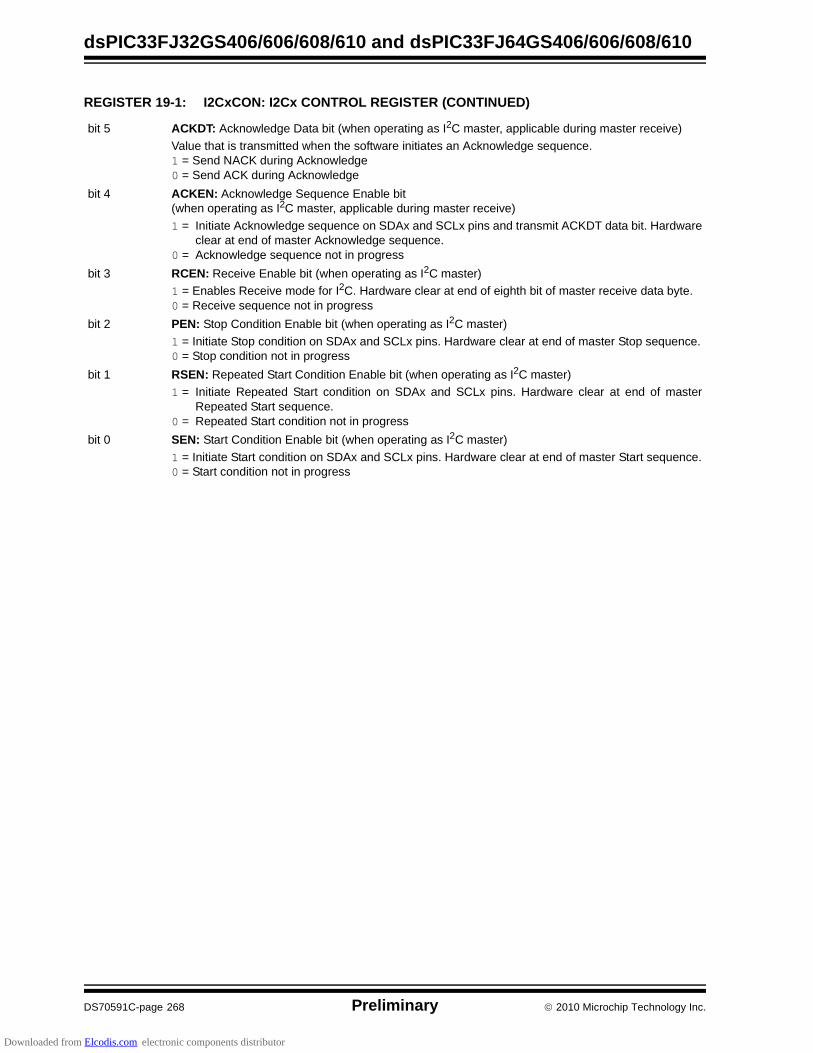
dsPIC33FJ32GS406/606/608/610 and dsPIC33FJ64GS406/606/608/610
DS70591C-page 268 Preliminary 2010 Microchip Technology Inc.
bit 5 ACKDT: Acknowledge Data bit (when operating as I2C master, applicable during master receive)
Value that is transmitted when the software initiates an Acknowledge sequence.1 = Send NACK during Acknowledge0 = Send ACK during Acknowledge
bit 4 ACKEN: Acknowledge Sequence Enable bit (when operating as I2C master, applicable during master receive)
1 = Initiate Acknowledge sequence on SDAx and SCLx pins and transmit ACKDT data bit. Hardwareclear at end of master Acknowledge sequence.
0 = Acknowledge sequence not in progress
bit 3 RCEN: Receive Enable bit (when operating as I2C master)
1 = Enables Receive mode for I2C. Hardware clear at end of eighth bit of master receive data byte.0 = Receive sequence not in progress
bit 2 PEN: Stop Condition Enable bit (when operating as I2C master)
1 = Initiate Stop condition on SDAx and SCLx pins. Hardware clear at end of master Stop sequence.0 = Stop condition not in progress
bit 1 RSEN: Repeated Start Condition Enable bit (when operating as I2C master)
1 = Initiate Repeated Start condition on SDAx and SCLx pins. Hardware clear at end of masterRepeated Start sequence.
0 = Repeated Start condition not in progress
bit 0 SEN: Start Condition Enable bit (when operating as I2C master)
1 = Initiate Start condition on SDAx and SCLx pins. Hardware clear at end of master Start sequence.0 = Start condition not in progress
REGISTER 19-1: I2CxCON: I2Cx CONTROL REGISTER (CONTINUED)
Downloaded from Elcodis.com electronic components distributor

2010 Microchip Technology Inc. Preliminary DS70591C-page 269
dsPIC33FJ32GS406/606/608/610 and dsPIC33FJ64GS406/606/608/610
REGISTER 19-2: I2CxSTAT: I2Cx STATUS REGISTER
R-0, HSC R-0, HSC U-0 U-0 U-0 R/C-0, HSC R-0, HSC R-0, HSC
ACKSTAT TRSTAT — — — BCL GCSTAT ADD10
bit 15 bit 8
R/C-0, HS R/C-0, HS R-0, HSC R/C-0, HSC R/C-0, HSC R-0, HSC R-0, HSC R-0, HSC
IWCOL I2COV D_A P S R_W RBF TBF
bit 7 bit 0
Legend: U = Unimplemented bit, read as ‘0’
R = Readable bit W = Writable bit HS = Hardware Settable bit HSC = Hardware Settable/Clearable
-n = Value at POR ‘1’ = Bit is set ‘0’ = Bit is cleared x = Bit is unknown
bit 15 ACKSTAT: Acknowledge Status bit (when operating as I2C master, applicable to master transmit operation)
1 = NACK received from slave0 = ACK received from slaveHardware set or clear at end of slave Acknowledge.
bit 14 TRSTAT: Transmit Status bit (when operating as I2C master, applicable to master transmit operation)
1 = Master transmit is in progress (8 bits + ACK)0 = Master transmit is not in progressHardware set at beginning of master transmission. Hardware clear at end of slave Acknowledge.
bit 13-11 Unimplemented: Read as ‘0’
bit 10 BCL: Master Bus Collision Detect bit
1 = A bus collision has been detected during a master operation0 = No collisionHardware set at detection of bus collision.
bit 9 GCSTAT: General Call Status bit
1 = General call address was received0 = General call address was not receivedHardware set when address matches general call address. Hardware clear at Stop detection.
bit 8 ADD10: 10-Bit Address Status bit
1 = 10-bit address was matched0 = 10-bit address was not matchedHardware set at match of 2nd byte of matched 10-bit address. Hardware clear at Stop detection.
bit 7 IWCOL: Write Collision Detect bit
1 = An attempt to write the I2CxTRN register failed because the I2C module is busy 0 = No collisionHardware set at occurrence of write to I2CxTRN while busy (cleared by software).
bit 6 I2COV: Receive Overflow Flag bit
1 = A byte was received while the I2CxRCV register is still holding the previous byte0 = No overflowHardware set at attempt to transfer I2CxRSR to I2CxRCV (cleared by software).
bit 5 D_A: Data/Address bit (when operating as I2C slave)
1 = Indicates that the last byte received was data0 = Indicates that the last byte received was device addressHardware clear at device address match. Hardware set by reception of slave byte.
bit 4 P: Stop bit
1 = Indicates that a Stop bit has been detected last0 = Stop bit was not detected lastHardware set or clear when Start, Repeated Start or Stop detected.
Downloaded from Elcodis.com electronic components distributor
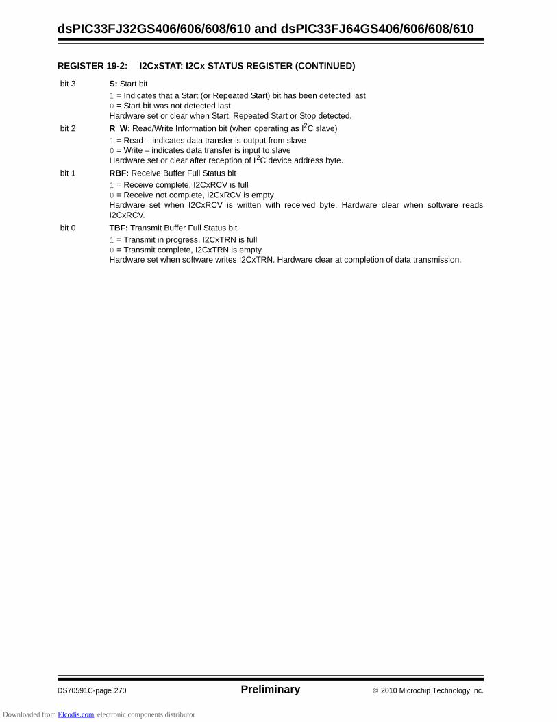
dsPIC33FJ32GS406/606/608/610 and dsPIC33FJ64GS406/606/608/610
DS70591C-page 270 Preliminary 2010 Microchip Technology Inc.
bit 3 S: Start bit
1 = Indicates that a Start (or Repeated Start) bit has been detected last0 = Start bit was not detected lastHardware set or clear when Start, Repeated Start or Stop detected.
bit 2 R_W: Read/Write Information bit (when operating as I2C slave)
1 = Read – indicates data transfer is output from slave0 = Write – indicates data transfer is input to slaveHardware set or clear after reception of I2C device address byte.
bit 1 RBF: Receive Buffer Full Status bit
1 = Receive complete, I2CxRCV is full0 = Receive not complete, I2CxRCV is emptyHardware set when I2CxRCV is written with received byte. Hardware clear when software readsI2CxRCV.
bit 0 TBF: Transmit Buffer Full Status bit
1 = Transmit in progress, I2CxTRN is full0 = Transmit complete, I2CxTRN is emptyHardware set when software writes I2CxTRN. Hardware clear at completion of data transmission.
REGISTER 19-2: I2CxSTAT: I2Cx STATUS REGISTER (CONTINUED)
Downloaded from Elcodis.com electronic components distributor

2010 Microchip Technology Inc. Preliminary DS70591C-page 271
dsPIC33FJ32GS406/606/608/610 and dsPIC33FJ64GS406/606/608/610
REGISTER 19-3: I2CxMSK: I2Cx SLAVE MODE ADDRESS MASK REGISTER
U-0 U-0 U-0 U-0 U-0 U-0 R/W-0 R/W-0
— — — — — — AMSK<9:8>
bit 15 bit 8
R/W-0 R/W-0 R/W-0 R/W-0 R/W-0 R/W-0 R/W-0 R/W-0
AMSK<7:0>
bit 7 bit 0
Legend:
R = Readable bit W = Writable bit U = Unimplemented bit, read as ‘0’
-n = Value at POR ‘1’ = Bit is set ‘0’ = Bit is cleared x = Bit is unknown
bit 15-10 Unimplemented: Read as ‘0’
bit 9-0 AMSK<9:0>: Mask for Address bit x Select bits
1 = Enable masking for bit x of incoming message address; bit match not required in this position0 = Disable masking for bit x; bit match required in this position
Downloaded from Elcodis.com electronic components distributor

dsPIC33FJ32GS406/606/608/610 and dsPIC33FJ64GS406/606/608/610
DS70591C-page 272 Preliminary 2010 Microchip Technology Inc.
NOTES:
Downloaded from Elcodis.com electronic components distributor

2010 Microchip Technology Inc. Preliminary DS70591C-page 273
dsPIC33FJ32GS406/606/608/610 and dsPIC33FJ64GS406/606/608/610
20.0 UNIVERSAL ASYNCHRONOUS RECEIVER TRANSMITTER (UART)
The Universal Asynchronous Receiver Transmitter(UART) module is one of the serial I/O modulesavailable in the dsPIC33FJ32GS406/606/608/610 anddsPIC33FJ64GS406/606/608/610 device families. TheUART is a full-duplex, asynchronous system that cancommunicate with peripheral devices, such aspersonal computers, LIN, RS-232 and RS-485interfaces. The module also supports a hardware flowcontrol option with the UxCTS and UxRTS pins andalso includes an IrDA encoder and decoder.
The primary features of the UART module are:
• Full-Duplex, 8-Bit or 9-Bit Data Transmission through the UxTX and UxRX pins
• Even, Odd or No Parity Options (for 8-bit data)
• One or Two Stop bits
• Hardware Flow Control Option with UxCTS and UxRTS Pins
• Fully Integrated Baud Rate Generator with 16-Bit Prescaler
• Baud Rates Ranging from 10 Mbps to 38 bps at40 MIPS
• 4-Deep First-In First-Out (FIFO) Transmit DataBuffer
• 4-Deep FIFO Receive Data Buffer
• Parity, Framing and Buffer Overrun Error Detection
• Support for 9-bit mode with Address Detect(9th bit = 1)
• Transmit and Receive Interrupts
• A Separate Interrupt for all UART Error Conditions
• Loopback mode for Diagnostic Support
• Support for Sync and Break Characters
• Support for Automatic Baud Rate Detection
• IrDA Encoder and Decoder Logic
• 16x Baud Clock Output for IrDA Support
• Support for DMA
A simplified block diagram of the UART module isshown in Figure 20-1. The UART module consists ofthese key hardware elements:
• Baud Rate Generator• Asynchronous Transmitter• Asynchronous Receiver
FIGURE 20-1: UART SIMPLIFIED BLOCK DIAGRAM
Note 1: This data sheet summarizes the featuresof the dsPIC33FJ32GS406/606/608/610and dsPIC33FJ64GS406/606/608/610families of devices. It is not intended to bea comprehensive reference source. Tocomplement the information in this datasheet, refer to Section 17. “UART”(DS70188) in the “dsPIC33F/PIC24HFamily Reference Manual”, which is avail-able from the Microchip web site(www.microchip.com).
2: Some registers and associated bitsdescribed in this section may not be avail-able on all devices. Refer to Section 4.0“Memory Organization” in this datasheet for device-specific register and bitinformation.
UxRX
Hardware Flow Control
UART Receiver
UART Transmitter UxTX
Baud Rate Generator
UxRTS
IrDA®
UxCTS
Downloaded from Elcodis.com electronic components distributor
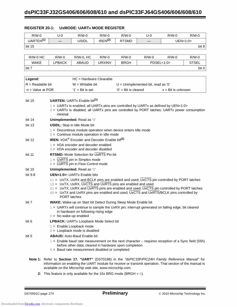
dsPIC33FJ32GS406/606/608/610 and dsPIC33FJ64GS406/606/608/610
DS70591C-page 274 Preliminary 2010 Microchip Technology Inc.
REGISTER 20-1: UxMODE: UARTx MODE REGISTER
R/W-0 U-0 R/W-0 R/W-0 R/W-0 U-0 R/W-0 R/W-0
UARTEN(1) — USIDL IREN(2) RTSMD — UEN<1:0>
bit 15 bit 8
R/W-0 HC R/W-0 R/W-0, HC R/W-0 R/W-0 R/W-0 R/W-0 R/W-0
WAKE LPBACK ABAUD URXINV BRGH PDSEL<1:0> STSEL
bit 7 bit 0
Legend: HC = Hardware Clearable
R = Readable bit W = Writable bit U = Unimplemented bit, read as ‘0’
-n = Value at POR ‘1’ = Bit is set ‘0’ = Bit is cleared x = Bit is unknown
bit 15 UARTEN: UARTx Enable bit(1)
1 = UARTx is enabled; all UARTx pins are controlled by UARTx as defined by UEN<1:0>0 = UARTx is disabled; all UARTx pins are controlled by PORT latches; UARTx power consumption
minimal
bit 14 Unimplemented: Read as ‘0’
bit 13 USIDL: Stop in Idle Mode bit
1 = Discontinue module operation when device enters Idle mode0 = Continue module operation in Idle mode
bit 12 IREN: IrDA® Encoder and Decoder Enable bit(2)
1 = IrDA encoder and decoder enabled0 = IrDA encoder and decoder disabled
bit 11 RTSMD: Mode Selection for UxRTS Pin bit
1 = UxRTS pin in Simplex mode0 = UxRTS pin in Flow Control mode
bit 10 Unimplemented: Read as ‘0’
bit 9-8 UEN<1:0>: UARTx Enable bits
11 = UxTX, UxRX and BCLK pins are enabled and used; UxCTS pin controlled by PORT latches10 = UxTX, UxRX, UxCTS and UxRTS pins are enabled and used01 = UxTX, UxRX and UxRTS pins are enabled and used; UxCTS pin controlled by PORT latches00 = UxTX and UxRX pins are enabled and used; UxCTS and UxRTS/BCLK pins controlled by
PORT latches
bit 7 WAKE: Wake-up on Start bit Detect During Sleep Mode Enable bit
1 = UARTx will continue to sample the UxRX pin; interrupt generated on falling edge; bit cleared in hardware on following rising edge
0 = No wake-up enabled
bit 6 LPBACK: UARTx Loopback Mode Select bit
1 = Enable Loopback mode0 = Loopback mode is disabled
bit 5 ABAUD: Auto-Baud Enable bit
1 = Enable baud rate measurement on the next character – requires reception of a Sync field (55h)before other data; cleared in hardware upon completion
0 = Baud rate measurement disabled or completed
Note 1: Refer to Section 17. “UART” (DS70188) in the “dsPIC33F/PIC24H Family Reference Manual” forinformation on enabling the UART module for receive or transmit operation. That section of the manual isavailable on the Microchip web site, www.microchip.com.
2: This feature is only available for the 16x BRG mode (BRGH = 0).
Downloaded from Elcodis.com electronic components distributor
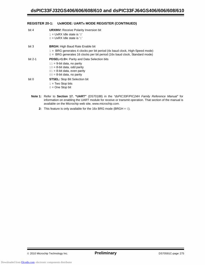
2010 Microchip Technology Inc. Preliminary DS70591C-page 275
dsPIC33FJ32GS406/606/608/610 and dsPIC33FJ64GS406/606/608/610
bit 4 URXINV: Receive Polarity Inversion bit
1 = UxRX Idle state is ‘0’0 = UxRX Idle state is ‘1’
bit 3 BRGH: High Baud Rate Enable bit
1 = BRG generates 4 clocks per bit period (4x baud clock, High-Speed mode)0 = BRG generates 16 clocks per bit period (16x baud clock, Standard mode)
bit 2-1 PDSEL<1:0>: Parity and Data Selection bits
11 = 9-bit data, no parity10 = 8-bit data, odd parity01 = 8-bit data, even parity00 = 8-bit data, no parity
bit 0 STSEL: Stop Bit Selection bit
1 = Two Stop bits0 = One Stop bit
REGISTER 20-1: UxMODE: UARTx MODE REGISTER (CONTINUED)
Note 1: Refer to Section 17. “UART” (DS70188) in the “dsPIC33F/PIC24H Family Reference Manual” forinformation on enabling the UART module for receive or transmit operation. That section of the manual isavailable on the Microchip web site, www.microchip.com.
2: This feature is only available for the 16x BRG mode (BRGH = 0).
Downloaded from Elcodis.com electronic components distributor

dsPIC33FJ32GS406/606/608/610 and dsPIC33FJ64GS406/606/608/610
DS70591C-page 276 Preliminary 2010 Microchip Technology Inc.
REGISTER 20-2: UxSTA: UARTx STATUS AND CONTROL REGISTER
R/W-0 R/W-0 R/W-0 U-0 R/W-0, HC R/W-0 R-0 R-1
UTXISEL1 UTXINV UTXISEL0 — UTXBRK UTXEN(1) UTXBF TRMT
bit 15 bit 8
R/W-0 R/W-0 R/W-0 R-1 R-0 R-0 R/C-0 R-0
URXISEL<1:0> ADDEN RIDLE PERR FERR OERR URXDA
bit 7 bit 0
Legend: HC = Hardware Clearable bit C = Clearable bit
R = Readable bit W = Writable bit U = Unimplemented bit, read as ‘0’
-n = Value at POR ‘1’ = Bit is set ‘0’ = Bit is cleared x = Bit is unknown
bit 15,13 UTXISEL<1:0>: Transmission Interrupt Mode Selection bits
11 = Reserved; do not use10 = Interrupt when a character is transferred to the Transmit Shift register, and as a result, the
transmit buffer becomes empty01 = Interrupt when the last character is shifted out of the Transmit Shift register; all transmit
operations are completed00 = Interrupt when a character is transferred to the Transmit Shift register (this implies there is at
least one character open in the transmit buffer)
bit 14 UTXINV: Transmit Polarity Inversion bit
If IREN = 0:1 = UxTX Idle state is ‘0’0 = UxTX Idle state is ‘1’
If IREN = 1:
1 = IrDA® encoded UxTX Idle state is ‘1’0 = IrDA encoded UxTX Idle state is ‘0’
bit 12 Unimplemented: Read as ‘0’
bit 11 UTXBRK: Transmit Break bit
1 = Send Sync Break on next transmission – Start bit, followed by twelve ‘0’ bits, followed by Stop bit;cleared by hardware upon completion
0 = Sync Break transmission disabled or completed
bit 10 UTXEN: Transmit Enable bit(1)
1 = Transmit enabled, UxTX pin controlled by UARTx0 = Transmit disabled, any pending transmission is aborted and buffer is reset; UxTX pin controlled
by port
bit 9 UTXBF: Transmit Buffer Full Status bit (read-only)
1 = Transmit buffer is full0 = Transmit buffer is not full; at least one more character can be written
bit 8 TRMT: Transmit Shift Register Empty bit (read-only)
1 = Transmit Shift register is empty and transmit buffer is empty (the last transmission has completed)0 = Transmit Shift register is not empty, a transmission is in progress or queued
bit 7-6 URXISEL<1:0>: Receive Interrupt Mode Selection bits
11 = Interrupt is set on UxRSR transfer making the receive buffer full (i.e., has 4 data characters)10 = Interrupt is set on UxRSR transfer making the receive buffer 3/4 full (i.e., has 3 data characters)0x = Interrupt is set when any character is received and transferred from the UxRSR to the receive
buffer; receive buffer has one or more characters
Note 1: Refer to Section 17. “UART” (DS70188) in the “dsPIC33F/PIC24H Family Reference Manual” forinformation on enabling the UART module for transmit operation. That section of the manual is availableon the Microchip web site, www.microchip.com.
Downloaded from Elcodis.com electronic components distributor

2010 Microchip Technology Inc. Preliminary DS70591C-page 277
dsPIC33FJ32GS406/606/608/610 and dsPIC33FJ64GS406/606/608/610
bit 5 ADDEN: Address Character Detect bit (bit 8 of received data = 1)
1 = Address Detect mode enabled. If 9-bit mode is not selected, this does not take effect.0 = Address Detect mode disabled
bit 4 RIDLE: Receiver Idle bit (read-only)
1 = Receiver is Idle0 = Receiver is active
bit 3 PERR: Parity Error Status bit (read-only)
1 = Parity error has been detected for the current character (character at the top of the receive FIFO)0 = Parity error has not been detected
bit 2 FERR: Framing Error Status bit (read-only)
1 = Framing error has been detected for the current character (character at the top of the receiveFIFO)
0 = Framing error has not been detected
bit 1 OERR: Receive Buffer Overrun Error Status bit (clear/read-only)
1 = Receive buffer has overflowed0 = Receive buffer has not overflowed. Clearing a previously set OERR bit (1 0 transition) will reset
the receiver buffer and the UxRSR to the empty state.
bit 0 URXDA: Receive Buffer Data Available bit (read-only)
1 = Receive buffer has data, at least one more character can be read0 = Receive buffer is empty
REGISTER 20-2: UxSTA: UARTx STATUS AND CONTROL REGISTER (CONTINUED)
Note 1: Refer to Section 17. “UART” (DS70188) in the “dsPIC33F/PIC24H Family Reference Manual” forinformation on enabling the UART module for transmit operation. That section of the manual is availableon the Microchip web site, www.microchip.com.
Downloaded from Elcodis.com electronic components distributor
dsPIC33FJ32GS406/606/608/610 and dsPIC33FJ64GS406/606/608/610
DS70591C-page 278 Preliminary 2010 Microchip Technology Inc.
NOTES:
Downloaded from Elcodis.com electronic components distributor

2010 Microchip Technology Inc. Preliminary DS70591C-page 279
dsPIC33FJ32GS406/606/608/610 and dsPIC33FJ64GS406/606/608/610
21.0 ENHANCED CAN (ECAN™) MODULE
21.1 Overview
The Enhanced Controller Area Network (ECAN) mod-ule is a serial interface, useful for communicating withother CAN modules or microcontroller devices. Thisinterface/protocol was designed to allow communica-tions within noisy environments. ThedsPIC33FJ32GS406/606/608/610 anddsPIC33FJ64GS406/606/608/610 devices contain upto two ECAN modules.
The ECAN module is a communication controller imple-menting the CAN 2.0 A/B protocol, as defined in theBOSCH CAN specification. The module supportsCAN 1.2, CAN 2.0A, CAN 2.0B Passive and CAN 2.0BActive versions of the protocol. The module implementa-tion is a full CAN system. The CAN specification is notcovered within this data sheet. The reader can refer tothe BOSCH CAN specification for further details.
The module features are as follows:
• Implementation of the CAN protocol, CAN 1.2, CAN 2.0A and CAN 2.0B
• Standard and extended data frames• 0-8 bytes data length
• Programmable bit rate up to 1 Mbit/sec• Automatic response to remote transmission
requests• Up to eight transmit buffers with application speci-
fied prioritization and abort capability (each buffer can contain up to 8 bytes of data)
• Up to 32 receive buffers (each buffer can contain up to 8 bytes of data)
• Up to 16 full (standard/extended identifier) acceptance filters
• Three full acceptance filter masks• DeviceNet™ addressing support• Programmable wake-up functionality with
integrated low-pass filter
• Programmable Loopback mode supports self-test operation
• Signaling via interrupt capabilities for all CAN receiver and transmitter error states
• Programmable clock source
• Programmable link to input capture module (IC2 for CAN1) for time-stamping and network synchronization
• Low-power Sleep and Idle mode
The CAN bus module consists of a protocol engine andmessage buffering/control. The CAN protocol enginehandles all functions for receiving and transmittingmessages on the CAN bus. Messages are transmittedby first loading the appropriate data registers. Statusand errors can be checked by reading the appropriateregisters. Any message detected on the CAN bus ischecked for errors and then matched against filters tosee if it should be received and stored in one of thereceive registers.
21.2 Frame TypesThe ECAN module transmits various types of frameswhich include data messages, or remote transmissionrequests initiated by the user, as other frames that areautomatically generated for control purposes. Thefollowing frame types are supported:
• Standard Data Frame:A standard data frame is generated by a node when the node wishes to transmit data. It includes an 11-bit Standard Identifier (SID), but not an 18-bit Extended Identifier (EID).
• Extended Data Frame:An extended data frame is similar to a standard data frame, but includes an extended identifier as well.
• Remote Frame:It is possible for a destination node to request the data from the source. For this purpose, the destination node sends a remote frame with an iden-tifier that matches the identifier of the required data frame. The appropriate data source node sends a data frame as a response to this remote request.
• Error Frame:An error frame is generated by any node that detects a bus error. An error frame consists of two fields: an error flag field and an error delimiter field.
• Overload Frame: An overload frame can be generated by a node as a result of two conditions. First, the node detects a dominant bit during interframe space which is an ille-gal condition. Second, due to internal conditions, the node is not yet able to start reception of the next message. A node can generate a maximum of 2 sequential overload frames to delay the start of the next message.
• Interframe Space:Interframe space separates a proceeding frame (of whatever type) from a following data or remote frame.
Note 1: This data sheet summarizes the featuresof the dsPIC33FJ32GS406/606/608/610and dsPIC33FJ64GS406/606/608/610families of devices. It is not intended to bea comprehensive reference source. Tocomplement the information in this datasheet, refer to Section 21. “EnhancedController Area Network (ECAN™)”(DS70185) in the dsPIC33F/PIC24HFamily Reference Manual, which is avail-able from the Microchip web site(www.microchip.com).
2: Some registers and associated bitsdescribed in this section may not be avail-able on all devices. Refer to Section 4.0“Memory Organization” in this datasheet for device-specific register and bitinformation.
Downloaded from Elcodis.com electronic components distributor
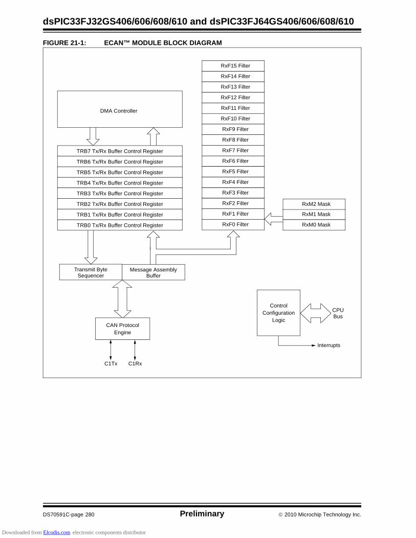
dsPIC33FJ32GS406/606/608/610 and dsPIC33FJ64GS406/606/608/610
DS70591C-page 280 Preliminary 2010 Microchip Technology Inc.
FIGURE 21-1: ECAN™ MODULE BLOCK DIAGRAM
Message Assembly
CAN ProtocolEngine
C1Tx
Buffer
C1Rx
RxF14 Filter
RxF13 Filter
RxF12 Filter
RxF11 Filter
RxF10 Filter
RxF9 Filter
RxF8 Filter
RxF7 Filter
RxF6 Filter
RxF5 Filter
RxF4 Filter
RxF3 Filter
RxF2 Filter
RxF1 Filter
RxF0 Filter
Transmit ByteSequencer
RxM1 Mask
RxM0 Mask
ControlConfiguration
Logic
CPUBus
Interrupts
TRB0 Tx/Rx Buffer Control Register
DMA Controller
RxF15 Filter
RxM2 Mask
TRB7 Tx/Rx Buffer Control Register
TRB6 Tx/Rx Buffer Control Register
TRB5 Tx/Rx Buffer Control Register
TRB4 Tx/Rx Buffer Control Register
TRB3 Tx/Rx Buffer Control Register
TRB2 Tx/Rx Buffer Control Register
TRB1 Tx/Rx Buffer Control Register
Downloaded from Elcodis.com electronic components distributor

2010 Microchip Technology Inc. Preliminary DS70591C-page 281
dsPIC33FJ32GS406/606/608/610 and dsPIC33FJ64GS406/606/608/610
21.3 Modes of Operation
The ECAN module can operate in one of severaloperation modes selected by the user. These modesinclude:
• Initialization mode• Disable mode• Normal Operation mode• Listen Only mode
• Listen All Messages mode
• Loopback mode
Modes are requested by setting the REQOP<2:0> bits(CiCTRL1<10:8>). Entry into a mode is Acknowledgedby monitoring the OPMODE<2:0> bits(CiCTRL1<7:5>). The module does not change themode and the OPMODE bits until a change in mode isacceptable, generally during bus Idle time, which isdefined as at least 11 consecutive recessive bits.
21.3.1 INITIALIZATION MODE
In the Initialization mode, the module does not transmitor receive. The error counters are cleared and the inter-rupt flags remain unchanged. The user application hasaccess to Configuration registers that are accessrestricted in other modes. The module protects the userfrom accidentally violating the CAN protocol throughprogramming errors. All registers which control theconfiguration of the module can not be modified whilethe module is on-line. The ECAN module is not allowedto enter the Configuration mode while a transmission istaking place. The Configuration mode serves as a lockto protect the following registers:
• All Module Control registers• Baud Rate and Interrupt Configuration registers • Bus Timing registers • Identifier Acceptance Filter registers • Identifier Acceptance Mask registers
21.3.2 DISABLE MODE
In Disable mode, the module does not transmit orreceive. The module has the ability to set the WAKIF bitdue to bus activity, however, any pending interruptsremains and the error counters retains their value.
If the REQOP<2:0> bits (CiCTRL1<10:8>) = 001, themodule enters the Module Disable mode. If the module isactive, the module waits for 11 recessive bits on the CANbus, detect that condition as an Idle bus, then accept themodule disable command. When the OPMODE<2:0>bits (CiCTRL1<7:5>) = 001, that indicates whether themodule successfully went into Module Disable mode.The I/O pins reverts to normal I/O function when themodule is in the Module Disable mode.
The module can be programmed to apply a low-passfilter function to the CiRX input line while the module orthe CPU is in Sleep mode. The WAKFIL bit(CiCFG2<14>) enables or disables the filter.
21.3.3 NORMAL OPERATION MODE
Normal Operation mode is selected whenREQOP<2:0> = 000. In this mode, the module isactivated and the I/O pins assumes the CAN busfunctions. The module transmits and receive CAN busmessages via the CiTX and CiRX pins.
21.3.4 LISTEN ONLY MODE
If the Listen Only mode is activated, the module on theCAN bus is passive. The transmitter buffers revert tothe port I/O function. The receive pins remain inputs.For the receiver, no error flags or Acknowledge signalsare sent. The error counters are deactivated in thisstate. The Listen Only mode can be used for detectingthe baud rate on the CAN bus. To use this, it is neces-sary that there are at least two further nodes thatcommunicate with each other.
21.3.5 LISTEN ALL MESSAGES MODE
The module can be set to ignore all errors and receiveany message. The Listen All Messages mode is acti-vated by setting REQOP<2:0> = ‘111’. In this mode,the data which is in the message assembly buffer, untilthe time an error occurred, is copied in the receive buf-fer and can be read via the CPU interface.
21.3.6 LOOPBACK MODE
If the Loopback mode is activated, the module con-nects the internal transmit signal to the internal receivesignal at the module boundary. The transmit andreceive pins revert to their port I/O function.
Note: Typically, if the ECAN module is allowed totransmit in a particular mode of operationand a transmission is requested immedi-ately after the ECAN module has beenplaced in that mode of operation, the mod-ule waits for 11 consecutive recessive bitson the bus before starting transmission. Ifthe user switches to Disable mode withinthis 11-bit period, then this transmission isaborted and the corresponding TXABT bitis set and TXREQ bit is cleared.
Downloaded from Elcodis.com electronic components distributor
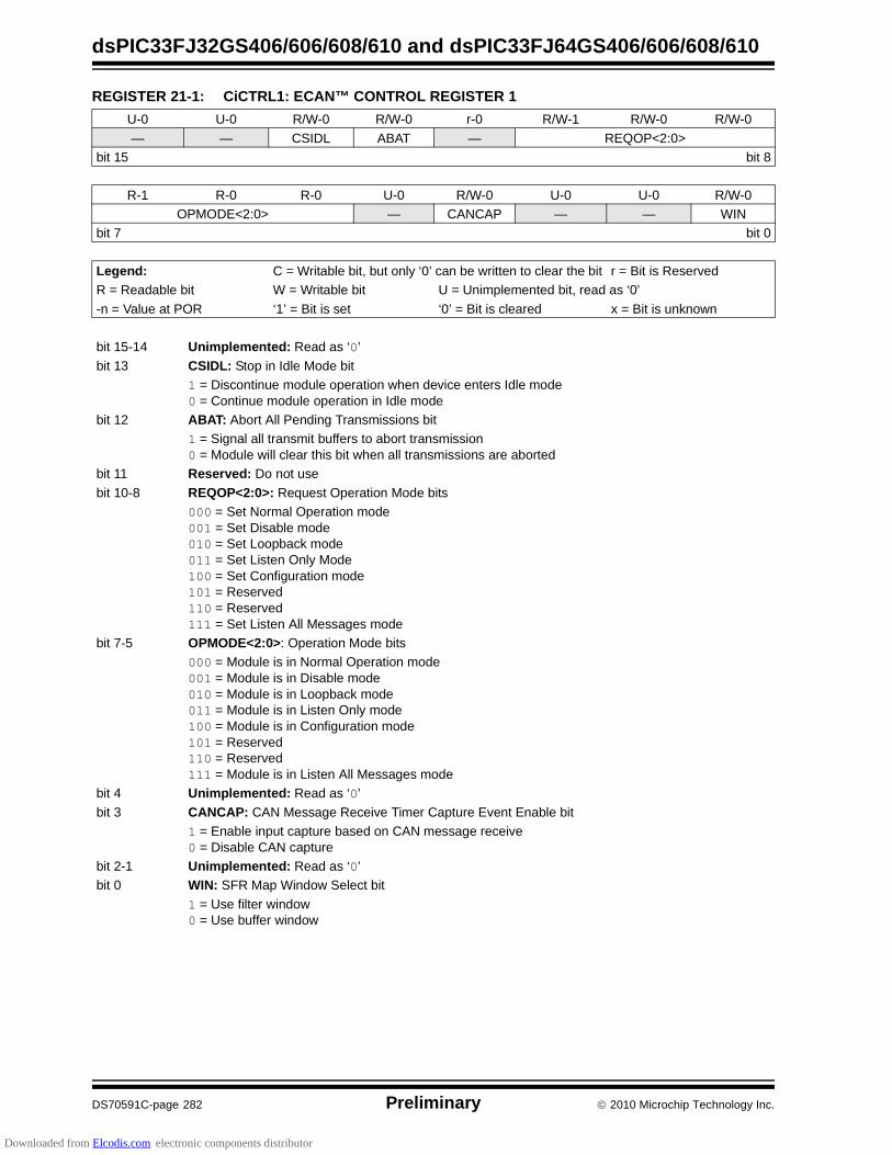
dsPIC33FJ32GS406/606/608/610 and dsPIC33FJ64GS406/606/608/610
DS70591C-page 282 Preliminary 2010 Microchip Technology Inc.
REGISTER 21-1: CiCTRL1: ECAN™ CONTROL REGISTER 1
U-0 U-0 R/W-0 R/W-0 r-0 R/W-1 R/W-0 R/W-0
— — CSIDL ABAT — REQOP<2:0>
bit 15 bit 8
R-1 R-0 R-0 U-0 R/W-0 U-0 U-0 R/W-0
OPMODE<2:0> — CANCAP — — WIN
bit 7 bit 0
Legend: C = Writable bit, but only ‘0’ can be written to clear the bit r = Bit is Reserved
R = Readable bit W = Writable bit U = Unimplemented bit, read as ‘0’
-n = Value at POR ‘1’ = Bit is set ‘0’ = Bit is cleared x = Bit is unknown
bit 15-14 Unimplemented: Read as ‘0’
bit 13 CSIDL: Stop in Idle Mode bit
1 = Discontinue module operation when device enters Idle mode0 = Continue module operation in Idle mode
bit 12 ABAT: Abort All Pending Transmissions bit
1 = Signal all transmit buffers to abort transmission0 = Module will clear this bit when all transmissions are aborted
bit 11 Reserved: Do not use
bit 10-8 REQOP<2:0>: Request Operation Mode bits
000 = Set Normal Operation mode001 = Set Disable mode010 = Set Loopback mode011 = Set Listen Only Mode100 = Set Configuration mode 101 = Reserved110 = Reserved 111 = Set Listen All Messages mode
bit 7-5 OPMODE<2:0>: Operation Mode bits
000 = Module is in Normal Operation mode001 = Module is in Disable mode010 = Module is in Loopback mode011 = Module is in Listen Only mode100 = Module is in Configuration mode101 = Reserved110 = Reserved111 = Module is in Listen All Messages mode
bit 4 Unimplemented: Read as ‘0’
bit 3 CANCAP: CAN Message Receive Timer Capture Event Enable bit
1 = Enable input capture based on CAN message receive 0 = Disable CAN capture
bit 2-1 Unimplemented: Read as ‘0’
bit 0 WIN: SFR Map Window Select bit
1 = Use filter window 0 = Use buffer window
Downloaded from Elcodis.com electronic components distributor

2010 Microchip Technology Inc. Preliminary DS70591C-page 283
dsPIC33FJ32GS406/606/608/610 and dsPIC33FJ64GS406/606/608/610
REGISTER 21-2: CiCTRL2: ECAN™ CONTROL REGISTER 2
U-0 U-0 U-0 U-0 U-0 U-0 U-0 U-0
— — — — — — — —
bit 15 bit 8
U-0 U-0 U-0 R-0 R-0 R-0 R-0 R-0
— — — DNCNT<4:0>
bit 7 bit 0
Legend: C = Writeable bit, but only ‘0’ can be written to clear the bit
R = Readable bit W = Writable bit U = Unimplemented bit, read as ‘0’
-n = Value at POR ‘1’ = Bit is set ‘0’ = Bit is cleared x = Bit is unknown
bit 15-5 Unimplemented: Read as ‘0’
bit 4-0 DNCNT<4:0>: DeviceNet™ Filter Bit Number bits
10010-11111 = Invalid selection 10001 = Compare up to data byte 3, bit 6 with EID<17>
•
•
•
00001 = Compare up to data byte 1, bit 7 with EID<0>00000 = Do not compare data bytes
Downloaded from Elcodis.com electronic components distributor

dsPIC33FJ32GS406/606/608/610 and dsPIC33FJ64GS406/606/608/610
DS70591C-page 284 Preliminary 2010 Microchip Technology Inc.
REGISTER 21-3: CiVEC: ECAN™ INTERRUPT CODE REGISTER
U-0 U-0 U-0 R-0 R-0 R-0 R-0 R-0
— — — FILHIT<4:0>
bit 15 bit 8
U-0 R-1 R-0 R-0 R-0 R-0 R-0 R-0
— ICODE<6:0>
bit 7 bit 0
Legend: C = Writeable bit, but only ‘0’ can be written to clear the bit
R = Readable bit W = Writable bit U = Unimplemented bit, read as ‘0’
-n = Value at POR ‘1’ = Bit is set ‘0’ = Bit is cleared x = Bit is unknown
bit 15-13 Unimplemented: Read as ‘0’
bit 12-8 FILHIT<4:0>: Filter Hit Number bits
10000-11111 = Reserved01111 = Filter 15
•
•
•
00001 = Filter 100000 = Filter 0
bit 7 Unimplemented: Read as ‘0’
bit 6-0 ICODE<6:0>: Interrupt Flag Code bits
1000101-1111111 = Reserved1000100 = FIFO almost full interrupt1000011 = Receiver overflow interrupt1000010 = Wake-up interrupt1000001 = Error interrupt1000000 = No interrupt
•
•
•
0010000-0111111 = Reserved0001111 = RB15 buffer Interrupt
•
•
•
0001001 = RB9 buffer interrupt 0001000 = RB8 buffer interrupt 0000111 = TRB7 buffer interrupt0000110 = TRB6 buffer interrupt0000101 = TRB5 buffer interrupt0000100 = TRB4 buffer interrupt0000011 = TRB3 buffer interrupt0000010 = TRB2 buffer interrupt0000001 = TRB1 buffer interrupt0000000 = TRB0 Buffer interrupt
Downloaded from Elcodis.com electronic components distributor

2010 Microchip Technology Inc. Preliminary DS70591C-page 285
dsPIC33FJ32GS406/606/608/610 and dsPIC33FJ64GS406/606/608/610
REGISTER 21-4: CiFCTRL: ECAN™ FIFO CONTROL REGISTER
R/W-0 R/W-0 R/W-0 U-0 U-0 U-0 U-0 U-0
DMABS<2:0> — — — — —
bit 15 bit 8
U-0 U-0 U-0 R/W-0 R/W-0 R/W-0 R/W-0 R/W-0
— — — FSA<4:0>
bit 7 bit 0
Legend: C = Writeable bit, but only ‘0’ can be written to clear the bit
R = Readable bit W = Writable bit U = Unimplemented bit, read as ‘0’
-n = Value at POR ‘1’ = Bit is set ‘0’ = Bit is cleared x = Bit is unknown
bit 15-13 DMABS<2:0>: DMA Buffer Size bits
111 = Reserved110 = 32 buffers in DMA RAM101 = 24 buffers in DMA RAM100 = 16 buffers in DMA RAM011 = 12 buffers in DMA RAM010 = 8 buffers in DMA RAM001 = 6 buffers in DMA RAM000 = 4 buffers in DMA RAM
bit 12-5 Unimplemented: Read as ‘0’
bit 4-0 FSA<4:0>: FIFO Area Starts with Buffer bits
11111 = Read buffer RB31 11110 = Read buffer RB30
•
•
•
00001 = Tx/Rx buffer TRB100000 = Tx/Rx buffer TRB0
Downloaded from Elcodis.com electronic components distributor
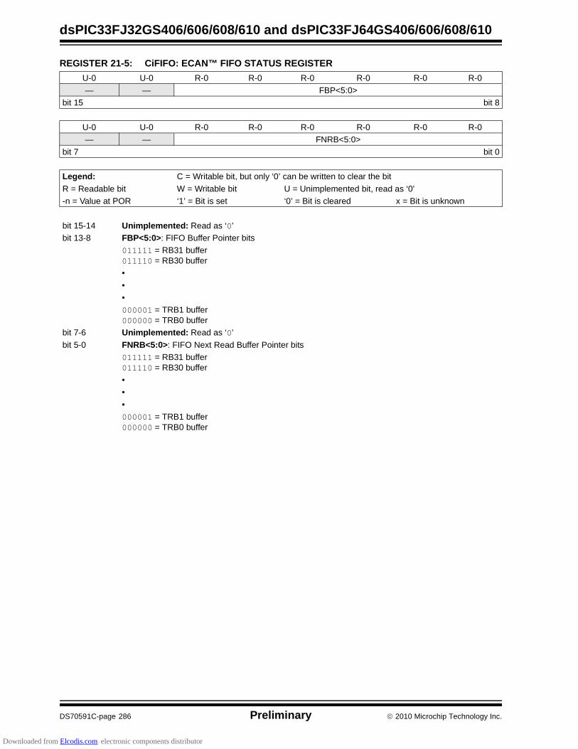
dsPIC33FJ32GS406/606/608/610 and dsPIC33FJ64GS406/606/608/610
DS70591C-page 286 Preliminary 2010 Microchip Technology Inc.
REGISTER 21-5: CiFIFO: ECAN™ FIFO STATUS REGISTER
U-0 U-0 R-0 R-0 R-0 R-0 R-0 R-0
— — FBP<5:0>
bit 15 bit 8
U-0 U-0 R-0 R-0 R-0 R-0 R-0 R-0
— — FNRB<5:0>
bit 7 bit 0
Legend: C = Writable bit, but only ‘0’ can be written to clear the bit
R = Readable bit W = Writable bit U = Unimplemented bit, read as ‘0’
-n = Value at POR ‘1’ = Bit is set ‘0’ = Bit is cleared x = Bit is unknown
bit 15-14 Unimplemented: Read as ‘0’
bit 13-8 FBP<5:0>: FIFO Buffer Pointer bits
011111 = RB31 buffer011110 = RB30 buffer
•
•
•
000001 = TRB1 buffer000000 = TRB0 buffer
bit 7-6 Unimplemented: Read as ‘0’
bit 5-0 FNRB<5:0>: FIFO Next Read Buffer Pointer bits
011111 = RB31 buffer011110 = RB30 buffer
•
•
•
000001 = TRB1 buffer000000 = TRB0 buffer
Downloaded from Elcodis.com electronic components distributor
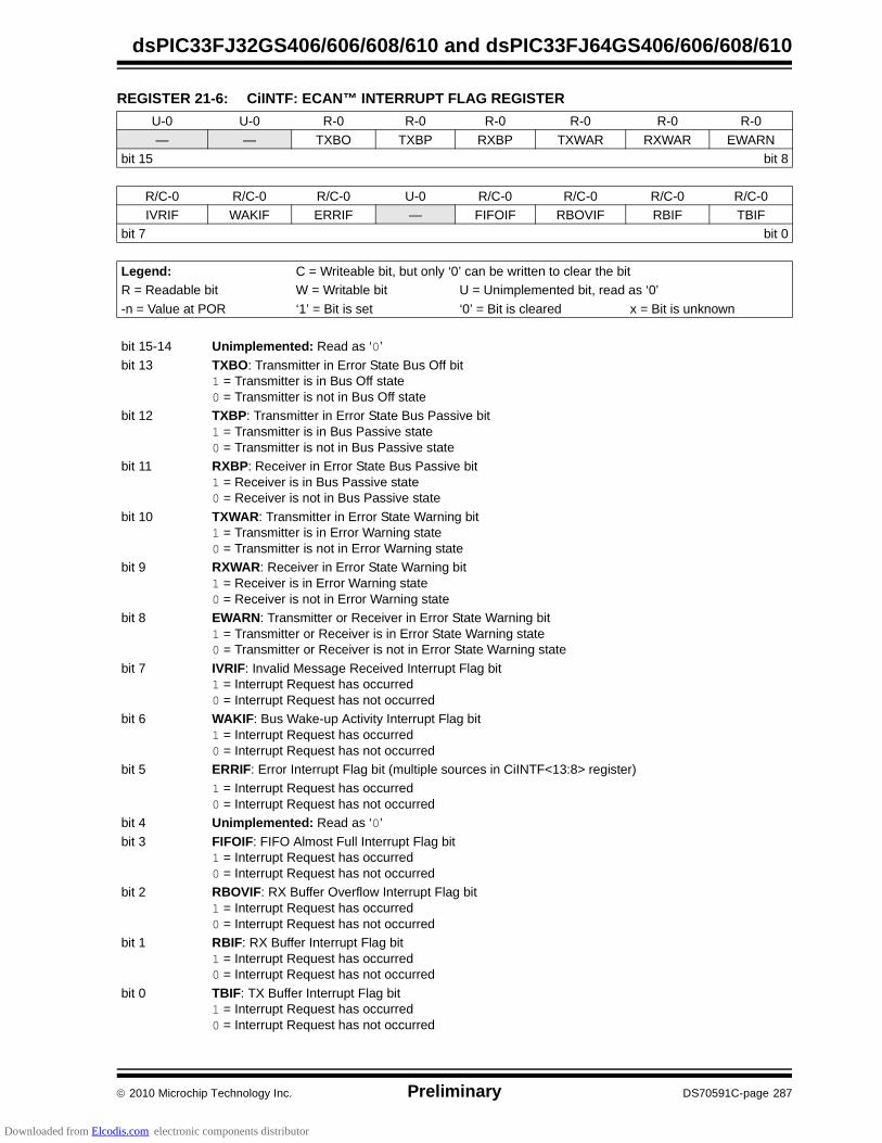
2010 Microchip Technology Inc. Preliminary DS70591C-page 287
dsPIC33FJ32GS406/606/608/610 and dsPIC33FJ64GS406/606/608/610
REGISTER 21-6: CiINTF: ECAN™ INTERRUPT FLAG REGISTER
U-0 U-0 R-0 R-0 R-0 R-0 R-0 R-0
— — TXBO TXBP RXBP TXWAR RXWAR EWARN
bit 15 bit 8
R/C-0 R/C-0 R/C-0 U-0 R/C-0 R/C-0 R/C-0 R/C-0
IVRIF WAKIF ERRIF — FIFOIF RBOVIF RBIF TBIF
bit 7 bit 0
Legend: C = Writeable bit, but only ‘0’ can be written to clear the bit
R = Readable bit W = Writable bit U = Unimplemented bit, read as ‘0’
-n = Value at POR ‘1’ = Bit is set ‘0’ = Bit is cleared x = Bit is unknown
bit 15-14 Unimplemented: Read as ‘0’
bit 13 TXBO: Transmitter in Error State Bus Off bit1 = Transmitter is in Bus Off state0 = Transmitter is not in Bus Off state
bit 12 TXBP: Transmitter in Error State Bus Passive bit1 = Transmitter is in Bus Passive state0 = Transmitter is not in Bus Passive state
bit 11 RXBP: Receiver in Error State Bus Passive bit1 = Receiver is in Bus Passive state0 = Receiver is not in Bus Passive state
bit 10 TXWAR: Transmitter in Error State Warning bit1 = Transmitter is in Error Warning state0 = Transmitter is not in Error Warning state
bit 9 RXWAR: Receiver in Error State Warning bit1 = Receiver is in Error Warning state0 = Receiver is not in Error Warning state
bit 8 EWARN: Transmitter or Receiver in Error State Warning bit1 = Transmitter or Receiver is in Error State Warning state0 = Transmitter or Receiver is not in Error State Warning state
bit 7 IVRIF: Invalid Message Received Interrupt Flag bit1 = Interrupt Request has occurred0 = Interrupt Request has not occurred
bit 6 WAKIF: Bus Wake-up Activity Interrupt Flag bit1 = Interrupt Request has occurred0 = Interrupt Request has not occurred
bit 5 ERRIF: Error Interrupt Flag bit (multiple sources in CiINTF<13:8> register)
1 = Interrupt Request has occurred0 = Interrupt Request has not occurred
bit 4 Unimplemented: Read as ‘0’
bit 3 FIFOIF: FIFO Almost Full Interrupt Flag bit1 = Interrupt Request has occurred0 = Interrupt Request has not occurred
bit 2 RBOVIF: RX Buffer Overflow Interrupt Flag bit1 = Interrupt Request has occurred0 = Interrupt Request has not occurred
bit 1 RBIF: RX Buffer Interrupt Flag bit1 = Interrupt Request has occurred0 = Interrupt Request has not occurred
bit 0 TBIF: TX Buffer Interrupt Flag bit1 = Interrupt Request has occurred0 = Interrupt Request has not occurred
Downloaded from Elcodis.com electronic components distributor

dsPIC33FJ32GS406/606/608/610 and dsPIC33FJ64GS406/606/608/610
DS70591C-page 288 Preliminary 2010 Microchip Technology Inc.
REGISTER 21-7: CiINTE: ECAN™ INTERRUPT ENABLE REGISTER
U-0 U-0 U-0 U-0 U-0 U-0 U-0 U-0
— — — — — — — —
bit 15 bit 8
R/W-0 R/W-0 R/W-0 R/W-0 R/W-0 R/W-0 R/W-0 R/W-0
IVRIE WAKIE ERRIE — FIFOIE RBOVIE RBIE TBIE
bit 7 bit 0
Legend: C = Writeable bit, but only ‘0’ can be written to clear the bit
R = Readable bit W = Writable bit U = Unimplemented bit, read as ‘0’
-n = Value at POR ‘1’ = Bit is set ‘0’ = Bit is cleared x = Bit is unknown
bit 15-8 Unimplemented: Read as ‘0’
bit 7 IVRIE: Invalid Message Received Interrupt Enable bit1 = Interrupt Request Enabled0 = Interrupt Request not enabled
bit 6 WAKIE: Bus Wake-up Activity Interrupt Flag bit1 = Interrupt Request Enabled0 = Interrupt Request not enabled
bit 5 ERRIE: Error Interrupt Enable bit
1 = Interrupt Request Enabled0 = Interrupt Request not enabled
bit 4 Unimplemented: Read as ‘0’
bit 3 FIFOIE: FIFO Almost Full Interrupt Enable bit1 = Interrupt Request Enabled0 = Interrupt Request not enabled
bit 2 RBOVIE: RX Buffer Overflow Interrupt Enable bit1 = Interrupt Request Enabled0 = Interrupt Request not enabled
bit 1 RBIE: RX Buffer Interrupt Enable bit1 = Interrupt Request Enabled0 = Interrupt Request not enabled
bit 0 TBIE: TX Buffer Interrupt Enable bit1 = Interrupt Request Enabled0 = Interrupt Request not enabled
Downloaded from Elcodis.com electronic components distributor

2010 Microchip Technology Inc. Preliminary DS70591C-page 289
dsPIC33FJ32GS406/606/608/610 and dsPIC33FJ64GS406/606/608/610
REGISTER 21-8: CiEC: ECAN™ TRANSMIT/RECEIVE ERROR COUNT REGISTER
R-0 R-0 R-0 R-0 R-0 R-0 R-0 R-0
TERRCNT<7:0>
bit 15 bit 8
R-0 R-0 R-0 R-0 R-0 R-0 R-0 R-0
RERRCNT<7:0>
bit 7 bit 0
Legend: C = Writeable bit, but only ‘0’ can be written to clear the bit
R = Readable bit W = Writable bit U = Unimplemented bit, read as ‘0’
-n = Value at POR ‘1’ = Bit is set ‘0’ = Bit is cleared x = Bit is unknown
bit 15-8 TERRCNT<7:0>: Transmit Error Count bits
bit 7-0 RERRCNT<7:0>: Receive Error Count bits
REGISTER 21-9: CiCFG1: ECAN™ BAUD RATE CONFIGURATION REGISTER 1
U-0 U-0 U-0 U-0 U-0 U-0 U-0 U-0
— — — — — — — —
bit 15 bit 8
R/W-0 R/W-0 R/W-0 R/W-0 R/W-0 R/W-0 R/W-0 R/W-0
SJW<1:0> BRP<5:0>
bit 7 bit 0
Legend:
R = Readable bit W = Writable bit U = Unimplemented bit, read as ‘0’
-n = Value at POR ‘1’ = Bit is set ‘0’ = Bit is cleared x = Bit is unknown
bit 15-8 Unimplemented: Read as ‘0’
bit 7-6 SJW<1:0>: Synchronization Jump Width bits
11 = Length is 4 x TQ 10 = Length is 3 x TQ 01 = Length is 2 x TQ 00 = Length is 1 x TQ
bit 5-0 BRP<5:0>: Baud Rate Prescaler bits
11 1111 = TQ = 2 x 64 x 1/FCAN
•
•
•
00 0010 = TQ = 2 x 3 x 1/FCAN
00 0001 = TQ = 2 x 2 x 1/FCAN 00 0000 = TQ = 2 x 1 x 1/FCAN
Downloaded from Elcodis.com electronic components distributor

dsPIC33FJ32GS406/606/608/610 and dsPIC33FJ64GS406/606/608/610
DS70591C-page 290 Preliminary 2010 Microchip Technology Inc.
REGISTER 21-10: CiCFG2: ECAN™ BAUD RATE CONFIGURATION REGISTER 2
U-0 R/W-x U-0 U-0 U-0 R/W-x R/W-x R/W-x
— WAKFIL — — — SEG2PH<2:0>
bit 15 bit 8
R/W-x R/W-x R/W-x R/W-x R/W-x R/W-x R/W-x R/W-x
SEG2PHTS SAM SEG1PH<2:0> PRSEG<2:0>
bit 7 bit 0
Legend:
R = Readable bit W = Writable bit U = Unimplemented bit, read as ‘0’
-n = Value at POR ‘1’ = Bit is set ‘0’ = Bit is cleared x = Bit is unknown
bit 15 Unimplemented: Read as ‘0’
bit 14 WAKFIL: Select CAN bus Line Filter for Wake-up bit
1 = Use CAN bus line filter for wake-up0 = CAN bus line filter is not used for wake-up
bit 13-11 Unimplemented: Read as ‘0’
bit 10-8 SEG2PH<2:0>: Phase Segment 2 bits
111 = Length is 8 x TQ
•
•
•
000 = Length is 1 x TQ
bit 7 SEG2PHTS: Phase Segment 2 Time Select bit
1 = Freely programmable0 = Maximum of SEG1PH bits or Information Processing Time (IPT), whichever is greater
bit 6 SAM: Sample of the CAN bus Line bit
1 = Bus line is sampled three times at the sample point 0 = Bus line is sampled once at the sample point
bit 5-3 SEG1PH<2:0>: Phase Segment 1 bits
111 = Length is 8 x TQ
•
•
•
000 = Length is 1 x TQ
bit 2-0 PRSEG<2:0>: Propagation Time Segment bits
111 = Length is 8 x TQ
•
•
•
000 = Length is 1 x TQ
Downloaded from Elcodis.com electronic components distributor
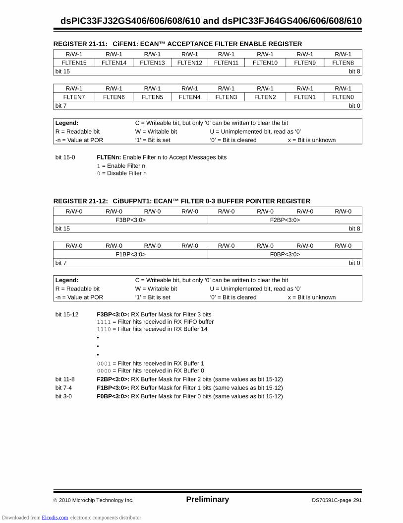
2010 Microchip Technology Inc. Preliminary DS70591C-page 291
dsPIC33FJ32GS406/606/608/610 and dsPIC33FJ64GS406/606/608/610
REGISTER 21-11: CiFEN1: ECAN™ ACCEPTANCE FILTER ENABLE REGISTER
R/W-1 R/W-1 R/W-1 R/W-1 R/W-1 R/W-1 R/W-1 R/W-1
FLTEN15 FLTEN14 FLTEN13 FLTEN12 FLTEN11 FLTEN10 FLTEN9 FLTEN8
bit 15 bit 8
R/W-1 R/W-1 R/W-1 R/W-1 R/W-1 R/W-1 R/W-1 R/W-1
FLTEN7 FLTEN6 FLTEN5 FLTEN4 FLTEN3 FLTEN2 FLTEN1 FLTEN0
bit 7 bit 0
Legend: C = Writeable bit, but only ‘0’ can be written to clear the bit
R = Readable bit W = Writable bit U = Unimplemented bit, read as ‘0’
-n = Value at POR ‘1’ = Bit is set ‘0’ = Bit is cleared x = Bit is unknown
bit 15-0 FLTENn: Enable Filter n to Accept Messages bits
1 = Enable Filter n0 = Disable Filter n
REGISTER 21-12: CiBUFPNT1: ECAN™ FILTER 0-3 BUFFER POINTER REGISTER
R/W-0 R/W-0 R/W-0 R/W-0 R/W-0 R/W-0 R/W-0 R/W-0
F3BP<3:0> F2BP<3:0>
bit 15 bit 8
R/W-0 R/W-0 R/W-0 R/W-0 R/W-0 R/W-0 R/W-0 R/W-0
F1BP<3:0> F0BP<3:0>
bit 7 bit 0
Legend: C = Writeable bit, but only ‘0’ can be written to clear the bit
R = Readable bit W = Writable bit U = Unimplemented bit, read as ‘0’
-n = Value at POR ‘1’ = Bit is set ‘0’ = Bit is cleared x = Bit is unknown
bit 15-12 F3BP<3:0>: RX Buffer Mask for Filter 3 bits1111 = Filter hits received in RX FIFO buffer1110 = Filter hits received in RX Buffer 14
•
•
•
0001 = Filter hits received in RX Buffer 10000 = Filter hits received in RX Buffer 0
bit 11-8 F2BP<3:0>: RX Buffer Mask for Filter 2 bits (same values as bit 15-12)
bit 7-4 F1BP<3:0>: RX Buffer Mask for Filter 1 bits (same values as bit 15-12)
bit 3-0 F0BP<3:0>: RX Buffer Mask for Filter 0 bits (same values as bit 15-12)
Downloaded from Elcodis.com electronic components distributor

dsPIC33FJ32GS406/606/608/610 and dsPIC33FJ64GS406/606/608/610
DS70591C-page 292 Preliminary 2010 Microchip Technology Inc.
REGISTER 21-13: CiBUFPNT2: ECAN™ FILTER 4-7 BUFFER POINTER REGISTER
R/W-0 R/W-0 R/W-0 R/W-0 R/W-0 R/W-0 R/W-0 R/W-0
F7BP<3:0> F6BP<3:0>
bit 15 bit 8
R/W-0 R/W-0 R/W-0 R/W-0 R/W-0 R/W-0 R/W-0 R/W-0
F5BP<3:0> F4BP<3:0>
bit 7 bit 0
Legend: C = Writeable bit, but only ‘0’ can be written to clear the bit
R = Readable bit W = Writable bit U = Unimplemented bit, read as ‘0’
-n = Value at POR ‘1’ = Bit is set ‘0’ = Bit is cleared x = Bit is unknown
bit 15-12 F7BP<3:0>: RX Buffer Mask for Filter 7 bits1111 = Filter hits received in RX FIFO buffer1110 = Filter hits received in RX Buffer 14
•
•
•
0001 = Filter hits received in RX Buffer 10000 = Filter hits received in RX Buffer 0
bit 11-8 F6BP<3:0>: RX Buffer Mask for Filter 6 bits (same values as bit 15-12)
bit 7-4 F5BP<3:0>: RX Buffer Mask for Filter 5 bits (same values as bit 15-12)
bit 3-0 F4BP<3:0>: RX Buffer Mask for Filter 4 bits (same values as bit 15-12)
REGISTER 21-14: CiBUFPNT3: ECAN™ FILTER 8-11 BUFFER POINTER REGISTER
R/W-0 R/W-0 R/W-0 R/W-0 R/W-0 R/W-0 R/W-0 R/W-0
F11BP<3:0> F10BP<3:0>
bit 15 bit 8
R/W-0 R/W-0 R/W-0 R/W-0 R/W-0 R/W-0 R/W-0 R/W-0
F9BP<3:0> F8BP<3:0>
bit 7 bit 0
Legend: C = Writeable bit, but only ‘0’ can be written to clear the bit
R = Readable bit W = Writable bit U = Unimplemented bit, read as ‘0’
-n = Value at POR ‘1’ = Bit is set ‘0’ = Bit is cleared x = Bit is unknown
bit 15-12 F11BP<3:0>: RX Buffer Mask for Filter 11 bits1111 = Filter hits received in RX FIFO buffer1110 = Filter hits received in RX Buffer 14
•
•
•
0001 = Filter hits received in RX Buffer 10000 = Filter hits received in RX Buffer 0
bit 11-8 F10BP<3:0>: RX Buffer Mask for Filter 10 bits (same values as bit 15-12)
bit 7-4 F9BP<3:0>: RX Buffer Mask for Filter 9 bits (same values as bit 15-12)
bit 3-0 F8BP<3:0>: RX Buffer Mask for Filter 8 bits (same values as bit 15-12)
Downloaded from Elcodis.com electronic components distributor
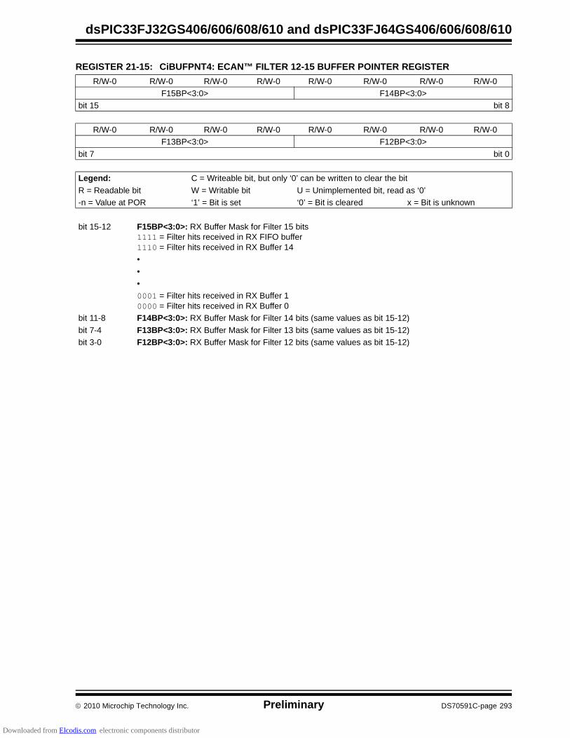
2010 Microchip Technology Inc. Preliminary DS70591C-page 293
dsPIC33FJ32GS406/606/608/610 and dsPIC33FJ64GS406/606/608/610
REGISTER 21-15: CiBUFPNT4: ECAN™ FILTER 12-15 BUFFER POINTER REGISTER
R/W-0 R/W-0 R/W-0 R/W-0 R/W-0 R/W-0 R/W-0 R/W-0
F15BP<3:0> F14BP<3:0>
bit 15 bit 8
R/W-0 R/W-0 R/W-0 R/W-0 R/W-0 R/W-0 R/W-0 R/W-0
F13BP<3:0> F12BP<3:0>
bit 7 bit 0
Legend: C = Writeable bit, but only ‘0’ can be written to clear the bit
R = Readable bit W = Writable bit U = Unimplemented bit, read as ‘0’
-n = Value at POR ‘1’ = Bit is set ‘0’ = Bit is cleared x = Bit is unknown
bit 15-12 F15BP<3:0>: RX Buffer Mask for Filter 15 bits1111 = Filter hits received in RX FIFO buffer1110 = Filter hits received in RX Buffer 14
•
•
•
0001 = Filter hits received in RX Buffer 10000 = Filter hits received in RX Buffer 0
bit 11-8 F14BP<3:0>: RX Buffer Mask for Filter 14 bits (same values as bit 15-12)
bit 7-4 F13BP<3:0>: RX Buffer Mask for Filter 13 bits (same values as bit 15-12)
bit 3-0 F12BP<3:0>: RX Buffer Mask for Filter 12 bits (same values as bit 15-12)
Downloaded from Elcodis.com electronic components distributor
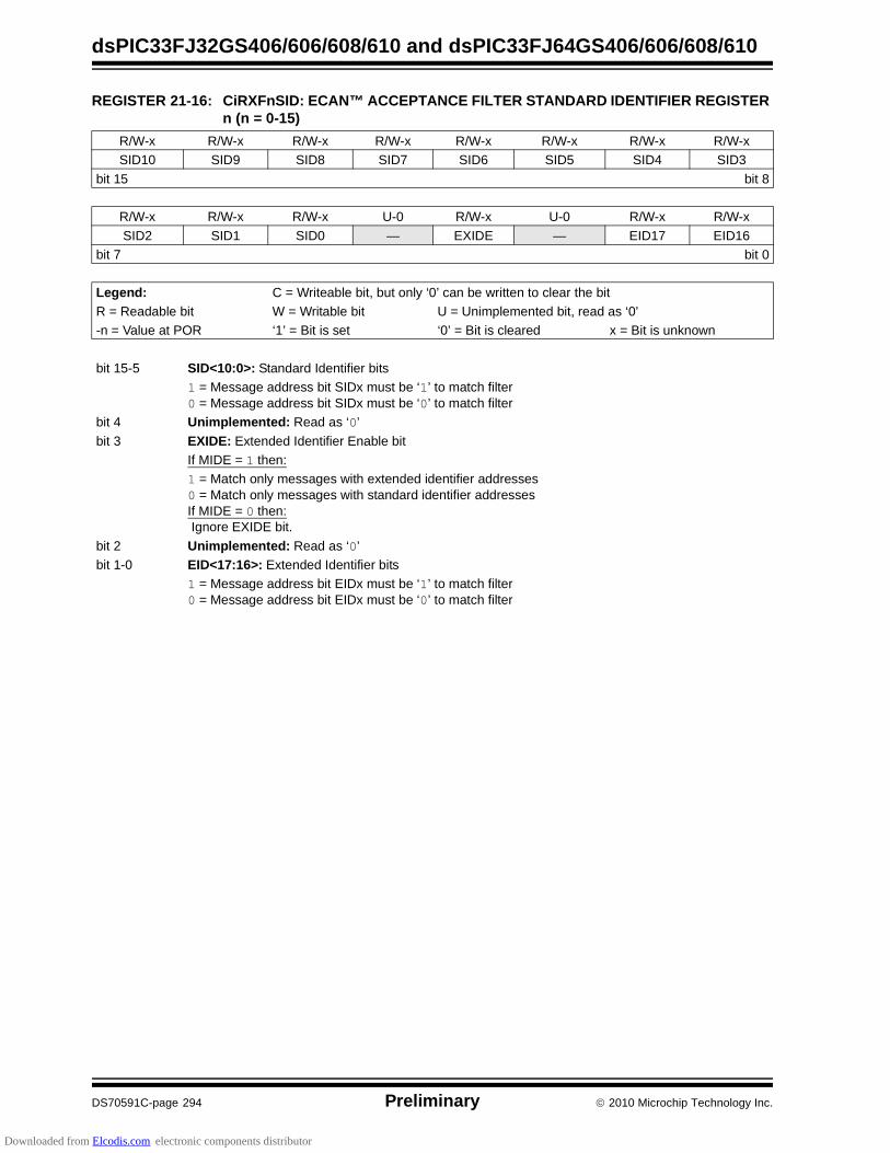
dsPIC33FJ32GS406/606/608/610 and dsPIC33FJ64GS406/606/608/610
DS70591C-page 294 Preliminary 2010 Microchip Technology Inc.
REGISTER 21-16: CiRXFnSID: ECAN™ ACCEPTANCE FILTER STANDARD IDENTIFIER REGISTER n (n = 0-15)
R/W-x R/W-x R/W-x R/W-x R/W-x R/W-x R/W-x R/W-x
SID10 SID9 SID8 SID7 SID6 SID5 SID4 SID3
bit 15 bit 8
R/W-x R/W-x R/W-x U-0 R/W-x U-0 R/W-x R/W-x
SID2 SID1 SID0 — EXIDE — EID17 EID16
bit 7 bit 0
Legend: C = Writeable bit, but only ‘0’ can be written to clear the bit
R = Readable bit W = Writable bit U = Unimplemented bit, read as ‘0’
-n = Value at POR ‘1’ = Bit is set ‘0’ = Bit is cleared x = Bit is unknown
bit 15-5 SID<10:0>: Standard Identifier bits
1 = Message address bit SIDx must be ‘1’ to match filter0 = Message address bit SIDx must be ‘0’ to match filter
bit 4 Unimplemented: Read as ‘0’
bit 3 EXIDE: Extended Identifier Enable bit
If MIDE = 1 then:
1 = Match only messages with extended identifier addresses0 = Match only messages with standard identifier addressesIf MIDE = 0 then: Ignore EXIDE bit.
bit 2 Unimplemented: Read as ‘0’
bit 1-0 EID<17:16>: Extended Identifier bits
1 = Message address bit EIDx must be ‘1’ to match filter0 = Message address bit EIDx must be ‘0’ to match filter
Downloaded from Elcodis.com electronic components distributor

2010 Microchip Technology Inc. Preliminary DS70591C-page 295
dsPIC33FJ32GS406/606/608/610 and dsPIC33FJ64GS406/606/608/610
REGISTER 21-17: CiRXFnEID: ECAN™ ACCEPTANCE FILTER EXTENDED IDENTIFIER REGISTER n (n = 0-15)
R/W-x R/W-x R/W-x R/W-x R/W-x R/W-x R/W-x R/W-x
EID15 EID14 EID13 EID12 EID11 EID10 EID9 EID8
bit 15 bit 8
R/W-x R/W-x R/W-x R/W-x R/W-x R/W-x R/W-x R/W-x
EID7 EID6 EID5 EID4 EID3 EID2 EID1 EID0
bit 7 bit 0
Legend: C = Writeable bit, but only ‘0’ can be written to clear the bit
R = Readable bit W = Writable bit U = Unimplemented bit, read as ‘0’
-n = Value at POR ‘1’ = Bit is set ‘0’ = Bit is cleared x = Bit is unknown
bit 15-0 EID<15:0>: Extended Identifier bits
1 = Message address bit EIDx must be ‘1’ to match filter0 = Message address bit EIDx must be ‘0’ to match filter
REGISTER 21-18: CiFMSKSEL1: ECAN™ FILTER 7-0 MASK SELECTION REGISTER
R/W-0 R/W-0 R/W-0 R/W-0 R/W-0 R/W-0 R/W-0 R/W-0
F7MSK<1:0> F6MSK<1:0> F5MSK<1:0> F4MSK<1:0>
bit 15 bit 8
R/W-0 R/W-0 R/W-0 R/W-0 R/W-0 R/W-0 R/W-0 R/W-0
F3MSK<1:0> F2MSK<1:0> F1MSK<1:0> F0MSK<1:0>
bit 7 bit 0
Legend: C = Writeable bit, but only ‘0’ can be written to clear the bit
R = Readable bit W = Writable bit U = Unimplemented bit, read as ‘0’
-n = Value at POR ‘1’ = Bit is set ‘0’ = Bit is cleared x = Bit is unknown
bit 15-14 F7MSK<1:0>: Mask Source for Filter 7 bits11 = Reserved10 = Acceptance Mask 2 registers contain mask01 = Acceptance Mask 1 registers contain mask00 = Acceptance Mask 0 registers contain mask
bit 13-12 F6MSK<1:0>: Mask Source for Filter 6 bits (same values as bit 15-14)
bit 11-10 F5MSK<1:0>: Mask Source for Filter 5 bits (same values as bit 15-14)
bit 9-8 F4MSK<1:0>: Mask Source for Filter 4 bits (same values as bit 15-14)
bit 7-6 F3MSK<1:0>: Mask Source for Filter 3 bits (same values as bit 15-14)
bit 5-4 F2MSK<1:0>: Mask Source for Filter 2 bits (same values as bit 15-14)
bit 3-2 F1MSK<1:0>: Mask Source for Filter 1 bits (same values as bit 15-14)
bit 1-0 F0MSK<1:0>: Mask Source for Filter 0 bits (same values as bit 15-14)
Downloaded from Elcodis.com electronic components distributor
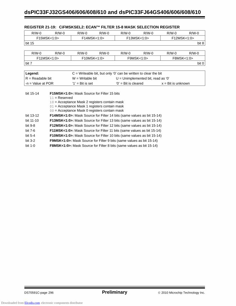
dsPIC33FJ32GS406/606/608/610 and dsPIC33FJ64GS406/606/608/610
DS70591C-page 296 Preliminary 2010 Microchip Technology Inc.
REGISTER 21-19: CiFMSKSEL2: ECAN™ FILTER 15-8 MASK SELECTION REGISTER
R/W-0 R/W-0 R/W-0 R/W-0 R/W-0 R/W-0 R/W-0 R/W-0
F15MSK<1:0> F14MSK<1:0> F13MSK<1:0> F12MSK<1:0>
bit 15 bit 8
R/W-0 R/W-0 R/W-0 R/W-0 R/W-0 R/W-0 R/W-0 R/W-0
F11MSK<1:0> F10MSK<1:0> F9MSK<1:0> F8MSK<1:0>
bit 7 bit 0
Legend: C = Writeable bit, but only ‘0’ can be written to clear the bit
R = Readable bit W = Writable bit U = Unimplemented bit, read as ‘0’
-n = Value at POR ‘1’ = Bit is set ‘0’ = Bit is cleared x = Bit is unknown
bit 15-14 F15MSK<1:0>: Mask Source for Filter 15 bits11 = Reserved10 = Acceptance Mask 2 registers contain mask01 = Acceptance Mask 1 registers contain mask00 = Acceptance Mask 0 registers contain mask
bit 13-12 F14MSK<1:0>: Mask Source for Filter 14 bits (same values as bit 15-14)
bit 11-10 F13MSK<1:0>: Mask Source for Filter 13 bits (same values as bit 15-14)
bit 9-8 F12MSK<1:0>: Mask Source for Filter 12 bits (same values as bit 15-14)
bit 7-6 F11MSK<1:0>: Mask Source for Filter 11 bits (same values as bit 15-14)
bit 5-4 F10MSK<1:0>: Mask Source for Filter 10 bits (same values as bit 15-14)
bit 3-2 F9MSK<1:0>: Mask Source for Filter 9 bits (same values as bit 15-14)
bit 1-0 F8MSK<1:0>: Mask Source for Filter 8 bits (same values as bit 15-14)
Downloaded from Elcodis.com electronic components distributor

2010 Microchip Technology Inc. Preliminary DS70591C-page 297
dsPIC33FJ32GS406/606/608/610 and dsPIC33FJ64GS406/606/608/610
REGISTER 21-20: CiRXMnSID: ECAN™ ACCEPTANCE FILTER MASK STANDARD IDENTIFIER REGISTER n (n = 0-2)
R/W-x R/W-x R/W-x R/W-x R/W-x R/W-x R/W-x R/W-x
SID10 SID9 SID8 SID7 SID6 SID5 SID4 SID3
bit 15 bit 8
R/W-x R/W-x R/W-x U-0 R/W-x U-0 R/W-x R/W-x
SID2 SID1 SID0 — MIDE — EID17 EID16
bit 7 bit 0
Legend: C = Writeable bit, but only ‘0’ can be written to clear the bit
R = Readable bit W = Writable bit U = Unimplemented bit, read as ‘0’
-n = Value at POR ‘1’ = Bit is set ‘0’ = Bit is cleared x = Bit is unknown
bit 15-5 SID<10:0>: Standard Identifier bits
1 = Include bit SIDx in filter comparison0 = Bit SIDx is don’t care in filter comparison
bit 4 Unimplemented: Read as ‘0’
bit 3 MIDE: Identifier Receive Mode bit
1 = Match only message types (standard or extended address) that correspond to EXIDE bit in filter 0 = Match either standard or extended address message if filters match
(i.e., if (Filter SID) = (Message SID) or if (Filter SID/EID) = (Message SID/EID))
bit 2 Unimplemented: Read as ‘0’
bit 1-0 EID<17:16>: Extended Identifier bits
1 = Include bit EIDx in filter comparison0 = Bit EIDx is don’t care in filter comparison
REGISTER 21-21: CiRXMnEID: ECAN™ ACCEPTANCE FILTER MASK EXTENDED IDENTIFIER REGISTER n (n = 0-2)
R/W-x R/W-x R/W-x R/W-x R/W-x R/W-x R/W-x R/W-x
EID15 EID14 EID13 EID12 EID11 EID10 EID9 EID8
bit 15 bit 8
R/W-x R/W-x R/W-x R/W-x R/W-x R/W-x R/W-x R/W-x
EID7 EID6 EID5 EID4 EID3 EID2 EID1 EID0
bit 7 bit 0
Legend: C = Writeable bit, but only ‘0’ can be written to clear the bit
R = Readable bit W = Writable bit U = Unimplemented bit, read as ‘0’
-n = Value at POR ‘1’ = Bit is set ‘0’ = Bit is cleared x = Bit is unknown
bit 15-0 EID<15:0>: Extended Identifier bits
1 = Include bit EIDx in filter comparison0 = Bit EIDx is don’t care in filter comparison
Downloaded from Elcodis.com electronic components distributor
dsPIC33FJ32GS406/606/608/610 and dsPIC33FJ64GS406/606/608/610
DS70591C-page 298 Preliminary 2010 Microchip Technology Inc.
REGISTER 21-22: CiRXFUL1: ECAN™ RECEIVE BUFFER FULL REGISTER 1
R/C-0 R/C-0 R/C-0 R/C-0 R/C-0 R/C-0 R/C-0 R/C-0
RXFUL15 RXFUL14 RXFUL13 RXFUL12 RXFUL11 RXFUL10 RXFUL9 RXFUL8
bit 15 bit 8
R/C-0 R/C-0 R/C-0 R/C-0 R/C-0 R/C-0 R/C-0 R/C-0
RXFUL7 RXFUL6 RXFUL5 RXFUL4 RXFUL3 RXFUL2 RXFUL1 RXFUL0
bit 7 bit 0
Legend: C = Writeable bit, but only ‘0’ can be written to clear the bit
R = Readable bit W = Writable bit U = Unimplemented bit, read as ‘0’
-n = Value at POR ‘1’ = Bit is set ‘0’ = Bit is cleared x = Bit is unknown
bit 15-0 RXFUL<15:0>: Receive Buffer n Full bits
1 = Buffer is full (set by module) 0 = Buffer is empty
REGISTER 21-23: CiRXFUL2: ECAN™ RECEIVE BUFFER FULL REGISTER 2
R/C-0 R/C-0 R/C-0 R/C-0 R/C-0 R/C-0 R/C-0 R/C-0
RXFUL31 RXFUL30 RXFUL29 RXFUL28 RXFUL27 RXFUL26 RXFUL25 RXFUL24
bit 15 bit 8
R/C-0 R/C-0 R/C-0 R/C-0 R/C-0 R/C-0 R/C-0 R/C-0
RXFUL23 RXFUL22 RXFUL21 RXFUL20 RXFUL19 RXFUL18 RXFUL17 RXFUL16
bit 7 bit 0
Legend: C = Writeable bit, but only ‘0’ can be written to clear the bit
R = Readable bit W = Writable bit U = Unimplemented bit, read as ‘0’
-n = Value at POR ‘1’ = Bit is set ‘0’ = Bit is cleared x = Bit is unknown
bit 15-0 RXFUL<31:16>: Receive Buffer n Full bits
1 = Buffer is full (set by module) 0 = Buffer is empty
Downloaded from Elcodis.com electronic components distributor

2010 Microchip Technology Inc. Preliminary DS70591C-page 299
dsPIC33FJ32GS406/606/608/610 and dsPIC33FJ64GS406/606/608/610
REGISTER 21-24: CiRXOVF1: ECAN™ RECEIVE BUFFER OVERFLOW REGISTER 1
R/C-0 R/C-0 R/C-0 R/C-0 R/C-0 R/C-0 R/C-0 R/C-0
RXOVF15 RXOVF14 RXOVF13 RXOVF12 RXOVF11 RXOVF10 RXOVF9 RXOVF8
bit 15 bit 8
R/C-0 R/C-0 R/C-0 R/C-0 R/C-0 R/C-0 R/C-0 R/C-0
RXOVF7 RXOVF6 RXOVF5 RXOVF4 RXOVF3 RXOVF2 RXOVF1 RXOVF0
bit 7 bit 0
Legend: C = Writeable bit, but only ‘0’ can be written to clear the bit
R = Readable bit W = Writable bit U = Unimplemented bit, read as ‘0’
-n = Value at POR ‘1’ = Bit is set ‘0’ = Bit is cleared x = Bit is unknown
bit 15-0 RXOVF<15:0>: Receive Buffer n Overflow bits
1 = Module attempted to write to a full buffer (set by module) 0 = No overflow condition
REGISTER 21-25: CiRXOVF2: ECAN™ RECEIVE BUFFER OVERFLOW REGISTER 2
R/C-0 R/C-0 R/C-0 R/C-0 R/C-0 R/C-0 R/C-0 R/C-0
RXOVF31 RXOVF30 RXOVF29 RXOVF28 RXOVF27 RXOVF26 RXOVF25 RXOVF24
bit 15 bit 8
R/C-0 R/C-0 R/C-0 R/C-0 R/C-0 R/C-0 R/C-0 R/C-0
RXOVF23 RXOVF22 RXOVF21 RXOVF20 RXOVF19 RXOVF18 RXOVF17 RXOVF16
bit 7 bit 0
Legend: C = Writeable bit, but only ‘0’ can be written to clear the bit
R = Readable bit W = Writable bit U = Unimplemented bit, read as ‘0’
-n = Value at POR ‘1’ = Bit is set ‘0’ = Bit is cleared x = Bit is unknown
bit 15-0 RXOVF<31:16>: Receive Buffer n Overflow bits
1 = Module attempted to write to a full buffer (set by module) 0 = No overflow condition
Downloaded from Elcodis.com electronic components distributor

dsPIC33FJ32GS406/606/608/610 and dsPIC33FJ64GS406/606/608/610
DS70591C-page 300 Preliminary 2010 Microchip Technology Inc.
REGISTER 21-26: CiTRmnCON: ECAN™ Tx/Rx BUFFER m CONTROL REGISTER(m = 0,2,4,6; n = 1,3,5,7)
R/W-0 R-0 R-0 R-0 R/W-0 R/W-0 R/W-0 R/W-0
TXENn TXABTn TXLARBn TXERRn TXREQn RTRENn TXnPRI<1:0>
bit 15 bit 8
R/W-0 R-0 R-0 R-0 R/W-0 R/W-0 R/W-0 R/W-0
TXENm TXABTm(1) TXLARBm(1) TXERRm(1) TXREQm RTRENm TXmPRI<1:0>
bit 7 bit 0
Legend: C = Writeable bit, but only ‘0’ can be written to clear the bit
R = Readable bit W = Writable bit U = Unimplemented bit, read as ‘0’
-n = Value at POR ‘1’ = Bit is set ‘0’ = Bit is cleared x = Bit is unknown
bit 15-8 See Definition for Bits 7-0, Controls Buffer n
bit 7 TXENm: TX/RX Buffer Selection bit
1 = Buffer TRBn is a transmit buffer0 = Buffer TRBn is a receive buffer
bit 6 TXABTm: Message Aborted bit(1)
1 = Message was aborted0 = Message completed transmission successfully
bit 5 TXLARBm: Message Lost Arbitration bit(1)
1 = Message lost arbitration while being sent0 = Message did not lose arbitration while being sent
bit 4 TXERRm: Error Detected During Transmission bit(1)
1 = A bus error occurred while the message was being sent0 = A bus error did not occur while the message was being sent
bit 3 TXREQm: Message Send Request bit
1 = Requests that a message be sent. The bit automatically clears when the message is successfullysent.
0 = Clearing the bit to ‘0’ while set requests a message abort.
bit 2 RTRENm: Auto-Remote Transmit Enable bit
1 = When a remote transmit is received, TXREQ will be set0 = When a remote transmit is received, TXREQ will be unaffected
bit 1-0 TXmPRI<1:0>: Message Transmission Priority bits
11 = Highest message priority10 = High intermediate message priority01 = Low intermediate message priority00 = Lowest message priority
Note 1: This bit is cleared when TXREQ is set.
Note: The buffers, SID, EID, DLC, Data Field and Receive Status registers are located in DMA RAM.
Downloaded from Elcodis.com electronic components distributor

2010 Microchip Technology Inc. Preliminary DS70591C-page 301
dsPIC33FJ32GS406/606/608/610 and dsPIC33FJ64GS406/606/608/610
21.4 ECAN Message Buffers
ECAN Message Buffers are part of DMA RAM Memory.They are not ECAN Special Function Registers. Theuser application must directly write into the DMA RAMarea that is configured for ECAN Message Buffers. Thelocation and size of the buffer area is defined by theuser application.
BUFFER 21-1: ECAN™ MESSAGE BUFFER WORD 0
U-0 U-0 U-0 R/W-x R/W-x R/W-x R/W-x R/W-x
— — — SID10 SID9 SID8 SID7 SID6
bit 15 bit 8
R/W-x R/W-x R/W-x R/W-x R/W-x R/W-x R/W-x R/W-x
SID5 SID4 SID3 SID2 SID1 SID0 SRR IDE
bit 7 bit 0
Legend:
R = Readable bit W = Writable bit U = Unimplemented bit, read as ‘0’
-n = Value at POR ‘1’ = Bit is set ‘0’ = Bit is cleared x = Bit is unknown
bit 15-13 Unimplemented: Read as ‘0’
bit 12-2 SID<10:0>: Standard Identifier bits
bit 1 SRR: Substitute Remote Request bit
1 = Message will request remote transmission 0 = Normal message
bit 0 IDE: Extended Identifier bit
1 = Message will transmit extended identifier 0 = Message will transmit standard identifier
BUFFER 21-2: ECAN™ MESSAGE BUFFER WORD 1
U-0 U-0 U-0 U-0 R/W-x R/W-x R/W-x R/W-x
— — — — EID17 EID16 EID15 EID14
bit 15 bit 8
R/W-x R/W-x R/W-x R/W-x R/W-x R/W-x R/W-x R/W-x
EID13 EID12 EID11 EID10 EID9 EID8 EID7 EID6
bit 7 bit 0
Legend:
R = Readable bit W = Writable bit U = Unimplemented bit, read as ‘0’
-n = Value at POR ‘1’ = Bit is set ‘0’ = Bit is cleared x = Bit is unknown
bit 15-12 Unimplemented: Read as ‘0’
bit 11-0 EID<17:6>: Extended Identifier bits
Downloaded from Elcodis.com electronic components distributor
dsPIC33FJ32GS406/606/608/610 and dsPIC33FJ64GS406/606/608/610
DS70591C-page 302 Preliminary 2010 Microchip Technology Inc.
(
BUFFER 21-3: ECAN™ MESSAGE BUFFER WORD 2
R/W-x R/W-x R/W-x R/W-x R/W-x R/W-x R/W-x R/W-x
EID5 EID4 EID3 EID2 EID1 EID0 RTR RB1
bit 15 bit 8
U-x U-x U-x R/W-x R/W-x R/W-x R/W-x R/W-x
— — — RB0 DLC3 DLC2 DLC1 DLC0
bit 7 bit 0
Legend:
R = Readable bit W = Writable bit U = Unimplemented bit, read as ‘0’
-n = Value at POR ‘1’ = Bit is set ‘0’ = Bit is cleared x = Bit is unknown
bit 15-10 EID<5:0>: Extended Identifier bits
bit 9 RTR: Remote Transmission Request bit
1 = Message will request remote transmission 0 = Normal message
bit 8 RB1: Reserved Bit 1
User must set this bit to ‘0’ per CAN protocol.
bit 7-5 Unimplemented: Read as ‘0’
bit 4 RB0: Reserved Bit 0
User must set this bit to ‘0’ per CAN protocol.
bit 3-0 DLC<3:0>: Data Length Code bits
BUFFER 21-4: ECAN™ MESSAGE BUFFER WORD 3
R/W-x R/W-x R/W-x R/W-x R/W-x R/W-x R/W-x R/W-x
Byte 1
bit 15 bit 8
R/W-x R/W-x R/W-x R/W-x R/W-x R/W-x R/W-x R/W-x
Byte 0
bit 7 bit 0
Legend:
R = Readable bit W = Writable bit U = Unimplemented bit, read as ‘0’
-n = Value at POR ‘1’ = Bit is set ‘0’ = Bit is cleared x = Bit is unknown
bit 15-8 Byte 1<15:8>: ECAN™ Message Byte 0
bit 7-0 Byte 0<7:0>: ECAN Message Byte 1
Downloaded from Elcodis.com electronic components distributor
2010 Microchip Technology Inc. Preliminary DS70591C-page 303
dsPIC33FJ32GS406/606/608/610 and dsPIC33FJ64GS406/606/608/610
BUFFER 21-5: ECAN™ MESSAGE BUFFER WORD 4
R/W-x R/W-x R/W-x R/W-x R/W-x R/W-x R/W-x R/W-x
Byte 3
bit 15 bit 8
R/W-x R/W-x R/W-x R/W-x R/W-x R/W-x R/W-x R/W-x
Byte 2
bit 7 bit 0
Legend:
R = Readable bit W = Writable bit U = Unimplemented bit, read as ‘0’
-n = Value at POR ‘1’ = Bit is set ‘0’ = Bit is cleared x = Bit is unknown
bit 15-8 Byte 3<15:8>: ECAN™ Message Byte 3
bit 7-0 Byte 2<7:0>: ECAN Message Byte 2
BUFFER 21-6: ECAN™ MESSAGE BUFFER WORD 5
R/W-x R/W-x R/W-x R/W-x R/W-x R/W-x R/W-x R/W-x
Byte 5
bit 15 bit 8
R/W-x R/W-x R/W-x R/W-x R/W-x R/W-x R/W-x R/W-x
Byte 4
bit 7 bit 0
Legend:
R = Readable bit W = Writable bit U = Unimplemented bit, read as ‘0’
-n = Value at POR ‘1’ = Bit is set ‘0’ = Bit is cleared x = Bit is unknown
bit 15-8 Byte 5<15:8>: ECAN™ Message Byte 5
bit 7-0 Byte 4<7:0>: ECAN Message Byte 4
Downloaded from Elcodis.com electronic components distributor

dsPIC33FJ32GS406/606/608/610 and dsPIC33FJ64GS406/606/608/610
DS70591C-page 304 Preliminary 2010 Microchip Technology Inc.
BUFFER 21-7: ECAN™ MESSAGE BUFFER WORD 6
R/W-x R/W-x R/W-x R/W-x R/W-x R/W-x R/W-x R/W-x
Byte 7
bit 15 bit 8
R/W-x R/W-x R/W-x R/W-x R/W-x R/W-x R/W-x R/W-x
Byte 6
bit 7 bit 0
Legend:
R = Readable bit W = Writable bit U = Unimplemented bit, read as ‘0’
-n = Value at POR ‘1’ = Bit is set ‘0’ = Bit is cleared x = Bit is unknown
bit 15-8 Byte 7<15:8>: ECAN™ Message Byte 7
bit 7-0 Byte 6<7:0>: ECAN Message Byte 6
BUFFER 21-8: ECAN™ MESSAGE BUFFER WORD 7
U-0 U-0 U-0 R/W-x R/W-x R/W-x R/W-x R/W-x
— — — FILHIT<4:0>(1)
bit 15 bit 8
U-0 U-0 U-0 U-0 U-0 U-0 U-0 U-0
— — — — — — — —
bit 7 bit 0
Legend:
R = Readable bit W = Writable bit U = Unimplemented bit, read as ‘0’
-n = Value at POR ‘1’ = Bit is set ‘0’ = Bit is cleared x = Bit is unknown
bit 15-13 Unimplemented: Read as ‘0’
bit 12-8 FILHIT<4:0>: Filter Hit Code bits(1)
Encodes number of filter that resulted in writing this buffer.
bit 7-0 Unimplemented: Read as ‘0’
Note 1: Only written by module for receive buffers, unused for transmit buffers.
Downloaded from Elcodis.com electronic components distributor

2010 Microchip Technology Inc. Preliminary DS70591C-page 305
dsPIC33FJ32GS406/606/608/610 and dsPIC33FJ64GS406/606/608/610
22.0 HIGH-SPEED 10-BIT ANALOG-TO-DIGITAL CONVERTER (ADC)
The dsPIC33FJ32GS406/606/608/610 anddsPIC33FJ64GS406/606/608/610 devices providehigh-speed successive approximation Analog-to-Digitalconversions to support applications such as AC/DC andDC/DC power converters.
22.1 Features Overview
The ADC module incorporates the following features:
• 10-bit resolution
• Unipolar inputs
• Up to two Successive Approximation Registers (SARs)
• Up to 24 external input channels
• Two internal analog inputs
• Dedicated result register for each analog input
• ±1 LSB accuracy at 3.3V
• Single supply operation
• 4 Msps conversion rate at 3.3V (devices with two SARs)
• 2 Msps conversion rate at 3.3V (devices with one SAR)
• Low-power CMOS technology
22.2 Module Description
This ADC module is designed for applications thatrequire low latency between the request for conversionand the resultant output data. Typical applicationsinclude:
• AC/DC power supplies• DC/DC converters• Power Factor Correction (PFC)
This ADC works with the high-speed PWM module inpower control applications that require high-frequencycontrol loops. This module can sample and convert twoanalog inputs in a 0.5 microsecond when two SARs areused. This small conversion delay reduces the “phaselag” between measurement and control systemresponse.
Up to five inputs may be sampled at a time (four inputsfrom the dedicated sample and hold circuits and onefrom the shared sample and hold circuit). If multipleinputs request conversion, the ADC will convert them ina sequential manner, starting with the lowest orderinput.
This ADC design provides each pair of analog inputs(AN1,AN0), (AN3,AN2),..., the ability to specify its owntrigger source out of a maximum of sixteen differenttrigger sources. This capability allows this ADC tosample and convert analog inputs that are associatedwith PWM generators operating on independent timebases.
The user application typically requires synchronizationbetween analog data sampling and PWM output to theapplication circuit. The very high-speed operation ofthis ADC module allows “data on demand”.
In addition, several hardware features have beenadded to the peripheral interface to improve real-timeperformance in a typical DSP-based application.
• Result alignment options
• Automated sampling
• External conversion start control
• Two internal inputs to monitor 1.2V internal reference and EXTREF input signal
A block diagram of the ADC module is shown in Figure 22-2.
Note 1: This data sheet summarizes the featuresof the dsPIC33FJ32GS406/606/608/610and dsPIC33FJ64GS406/606/608/610families of devices. It is not intended to bea comprehensive reference source. Tocomplement the information in this datasheet, refer to Section 44. “High-Speed10-Bit Analog-to-Digital Converter(ADC)” (DS70321) in the“dsPIC33F/PIC24H Family ReferenceManual”, which is available from theMicrochip web site (www.microchip.com).
2: Some registers and associated bitsdescribed in this section may not be avail-able on all devices. Refer to Section 4.0“Memory Organization” in this datasheet for device-specific register and bitinformation.
Downloaded from Elcodis.com electronic components distributor
dsPIC33FJ32GS406/606/608/610 and dsPIC33FJ64GS406/606/608/610
DS70591C-page 306 Preliminary 2010 Microchip Technology Inc.
22.3 Module Functionality
The high-speed 10-bit ADC is designed to supportpower conversion applications when used with theHigh-Speed PWM module. The ADC may have one ortwo SAR modules, depending on the device variant. Iftwo SARs are present on a device, two conversionscan be processed at a time, yielding 4 Msps conversionrate. If only one SAR is present on a device, only oneconversion can be processed at a time, yielding 2 Mspsconversion rate. The high-speed 10-bit ADC producestwo 10-bit conversion results in a 0.5 microsecond.
The ADC module supports up to 24 external analoginputs and two internal analog inputs. To monitorreference voltage, two internal inputs, AN24 and AN25,are connected to the EXTREF and internal band gapvoltages (1.2V), respectively.
The analog reference voltage is defined as the devicesupply voltage (AVDD/AVSS).
The ADC module uses the following control andSTATUS registers:
• ADCON: A/D Control Register
• ADSTAT: A/D Status Register
• ADBASE: A/D Base Register
• ADPCFG: A/D Port Configuration Register
• ADPCFG2: A/D Port Configuration Register 2
• ADCPC0: A/D Convert Pair Control Register 0
• ADCPC1: A/D Convert Pair Control Register 1
• ADCPC2: A/D Convert Pair Control Register 2
• ADCPC3: A/D Convert Pair Control Register 3
• ADCPC4: A/D Convert Pair Control Register 4
• ADCPC5: A/D Convert Pair Control Register 5
• ADCPC6: A/D Convert Pair Control Register 6
The ADCON register controls the operation of theADC module. The ADSTAT register displays thestatus of the conversion processes. The ADPCFGregisters configure the port pins as analog inputs oras digital I/O. The ADCPCx registers control thetriggering of the ADC conversions. See Register 22-1through Register 22-12 for detailed bit configurations.
Note: A unique feature of the ADC module is itsability to sample inputs in anasynchronous manner. Individual sampleand hold circuits can be triggeredindependently of each other.
Downloaded from Elcodis.com electronic components distributor

2010 Microchip Technology Inc. Preliminary DS70591C-page 307
dsPIC33FJ32GS406/606/608/610 and dsPIC33FJ64GS406/606/608/610
FIGURE 22-1: ADC BLOCK DIAGRAM FOR dsPIC33FJ32GS406 AND dsPIC33FJ64GS406 DEVICES WITH ONE SAR
Even Numbered Inputs with Dedicated
Shared Sample and HoldD
ata
For
mat
SARCore
Eight
Registers16-Bit
Sample and Hold (S&H) Circuits
Bus
Inte
rfac
e
AN0
AN1
AN7
AN15
AN3
AN2
AN4
AN6
AN5
AN24(1)
AN25(2)
(EXTREF)
(INTREF)
Note 1: AN24 (EXTREF) is an internal analog input. To measure the voltage at AN12 (EXTREF), an analog comparator must be enabledand EXTREF must be selected as the comparator reference.
2: AN25 (INTREF) is an internal analog input and is not available on a pin.
AN8
AN9
AN10
AN11
AN12
AN13
AN14
Downloaded from Elcodis.com electronic components distributor

dsPIC33FJ32GS406/606/608/610 and dsPIC33FJ64GS406/606/608/610
DS70591C-page 308 Preliminary 2010 Microchip Technology Inc.
FIGURE 22-2: ADC BLOCK DIAGRAM FOR dsPIC33FJ32GS606 AND dsPIC33FJ64GS606 DEVICES WITH TWO SARS
AN12
AN25(2)
Even Numbered Inputs with Dedicated
Odd Numbered Inputswith Shared S&H
Even Numbered Inputswith Shared S&H
Da
taF
orm
atSAR
Core
Seven
Registers16-Bit
SARCore
Sample and Hold (S&H) Circuits
Bus
Inte
rfa
ce
AN0
AN2
AN6
AN1
AN3
AN8
AN10
Da
taF
orm
at Seven
Registers16-Bit
AN4
AN5
AN7
AN9
AN11
(INTREF)
Note 1: AN24 (EXTREF) is an internal analog input. To measure the voltage at AN12 (EXTREF), an analog comparator must be enabled andEXTREF must be selected as the comparator reference.
2: AN25 (INTREF) is an internal analog input and is not available on a pin.
AN15
AN24(1)
(EXTREF)
AN14
AN13
Downloaded from Elcodis.com electronic components distributor
2010 Microchip Technology Inc. Preliminary DS70591C-page 309
dsPIC33FJ32GS406/606/608/610 and dsPIC33FJ64GS406/606/608/610
FIGURE 22-3: ADC BLOCK DIAGRAM FOR dsPIC33FJ32GS608 AND dsPIC33FJ64GS608 DEVICES WITH TWO SARS
AN25(2)
Even Numbered Inputs with Dedicated
Odd Numbered Inputswith Shared S&H
Even Numbered Inputswith Shared S&H
Dat
aF
orm
at
SAR
Core
Seven
Registers16-Bit
SAR
Core
Sample and Hold (S&H) Circuits
Bus
Inte
rfac
e
AN0
AN2
AN6
AN1
AN3
AN8
AN10
Dat
aF
orm
at
Seven
Registers16-Bit
AN4
AN5
AN7
AN9
AN11
(INTREF)
Note 1: AN24 (EXTREF) is an internal analog input. To measure the voltage at AN12 (EXTREF), an analog comparator must be enabled andEXTREF must be selected as the comparator reference.
2: AN25 (INTREF) is an internal analog input and is not available on a pin.
AN17
AN24(1)
(EXTREF)
AN13
AN15
AN12
AN14
AN16
Downloaded from Elcodis.com electronic components distributor

dsPIC33FJ32GS406/606/608/610 and dsPIC33FJ64GS406/606/608/610
DS70591C-page 310 Preliminary 2010 Microchip Technology Inc.
FIGURE 22-4: ADC BLOCK DIAGRAM FOR dsPIC33FJ32GS610 AND dsPIC33FJ64GS610 DEVICES WITH TWO SARS
AN25(2)
Even Numbered Inputs with Dedicated
Odd Numbered Inputswith Shared S&H
Even Numbered Inputswith Shared S&H
Da
taF
orm
atSAR
Core
Seven
Registers16-Bit
SAR
Core
Sample and Hold (S&H) Circuits
Bus
Inte
rfa
ce
AN0
AN2
AN6
AN1
AN3
AN8
AN10
Da
taF
orm
at Seven
Registers16-Bit
AN4
AN5
AN7
AN9
AN11
(INTREF)
Note 1: AN24 (EXTREF) is an internal analog input. To measure the voltage at AN12 (EXTREF), an analog comparator must be enabled andEXTREF must be selected as the comparator reference.
2: AN25 (INTREF) is an internal analog input and is not available on a pin.
AN24(1)
(EXTREF)
AN13
AN15
AN12
AN14
AN16
AN17
AN19
AN21
AN23
AN18
AN20
AN22
Downloaded from Elcodis.com electronic components distributor
2010 Microchip Technology Inc. Preliminary DS70591C-page 311
dsPIC33FJ32GS406/606/608/610 and dsPIC33FJ64GS406/606/608/610
REGISTER 22-1: ADCON: A/D CONTROL REGISTER
R/W-0 U-0 R/W-0 R/W-0 U-0 R/W-0 U-0 R/W-0
ADON — ADSIDL SLOWCLK(1) — GSWTRG — FORM(1)
bit 15 bit 8
R/W-0 R/W-0 R/W-0 R/W-0 U-0 R/W-0 R/W-1 R/W-1
EIE(1) ORDER(1) SEQSAMP(1) ASYNCSAMP(1) — ADCS<2:0>(1)
bit 7 bit 0
Legend:
R = Readable bit W = Writable bit U = Unimplemented bit, read as ‘0’
-n = Value at POR ‘1’ = Bit is set ‘0’ = Bit is cleared x = Bit is unknown
bit 15 ADON: A/D Operating Mode bit
1 = A/D converter module is operating0 = A/D converter is off
bit 14 Unimplemented: Read as ‘0’
bit 13 ADSIDL: Stop in Idle Mode bit
1 = Discontinue module operation when device enters Idle mode0 = Continue module operation in Idle mode
bit 12 SLOWCLK: Enable The Slow Clock Divider bit(1)
1 = ADC is clocked by the auxiliary PLL (ACLK)0 = ADC is clock by the primary PLL (FVCO)
bit 11 Unimplemented: Read as ‘0’
bit 10 GSWTRG: Global Software Trigger bit
When this bit is set by the user, it will trigger conversions if selected by the TRGSRC<4:0> bits in theADCPCx registers. This bit must be cleared by the user prior to initiating another global trigger (i.e., thisbit is not auto-clearing).
bit 9 Unimplemented: Read as ‘0’
bit 8 FORM: Data Output Format bit(1)
1 = Fractional (DOUT = dddd dddd dd00 0000)0 = Integer (DOUT = 0000 00dd dddd dddd)
bit 7 EIE: Early Interrupt Enable bit(1)
1 = Interrupt is generated after first conversion is completed0 = Interrupt is generated after second conversion is completed
bit 6 ORDER: Conversion Order bit(1)
1 = Odd numbered analog input is converted first, followed by conversion of even numbered input0 = Even numbered analog input is converted first, followed by conversion of odd numbered input
bit 5 SEQSAMP: Sequential Sample Enable bit(1)
1 = Shared Sample and Hold (S&H) circuit is sampled at the start of the second conversion ifORDER = 0. If ORDER = 1, then the shared S&H is sampled at the start of the first conversion.
0 = Shared S&H is sampled at the same time the dedicated S&H is sampled if the shared S&H is notcurrently busy with an existing conversion process. If the shared S&H is busy at the time thededicated S&H is sampled, then the shared S&H will sample at the start of the new conversioncycle.
bit 4 ASYNCSAMP: Asynchronous Dedicated S&H Sampling Enable bit(1)
1 = The dedicated S&H is constantly sampling and then terminates sampling as soon as the triggerpulse is detected.
0 = The dedicated S&H starts sampling when the trigger event is detected and completes the samplingprocess in two ADC clock cycles.
Note 1: This control bit can only be changed while the ADC is disabled (ADON = 0).
Downloaded from Elcodis.com electronic components distributor
dsPIC33FJ32GS406/606/608/610 and dsPIC33FJ64GS406/606/608/610
DS70591C-page 312 Preliminary 2010 Microchip Technology Inc.
bit 3 Unimplemented: Read as ‘0’
bit 2-0 ADCS<2:0>: A/D Conversion Clock Divider Select bits(1)
111 = FADC/8110 = FADC/7101 = FADC/6100 = FADC/5011 = FADC/4 (default)010 = FADC/3001 = FADC/2000 = FADC/1
REGISTER 22-1: ADCON: A/D CONTROL REGISTER (CONTINUED)
Note 1: This control bit can only be changed while the ADC is disabled (ADON = 0).
Downloaded from Elcodis.com electronic components distributor
2010 Microchip Technology Inc. Preliminary DS70591C-page 313
dsPIC33FJ32GS406/606/608/610 and dsPIC33FJ64GS406/606/608/610
REGISTER 22-2: ADSTAT: A/D STATUS REGISTER
U-0 U-0 U-0 R/C-0, HS R/C-0, HS R/C-0, HS R/C-0, HS R/C-0, HS
— — — P12RDY P11RDY P10RDY P9RDY P8RDY
bit 15 bit 8
R/C-0, HS R/C-0, HS R/C-0, HS R/C-0, HS R/C-0, HS R/C-0, HS R/C-0, HS R/C-0, HS
P7RDY P6RDY P5RDY P4RDY P3RDY P2RDY P1RDY P0RDY
bit 7 bit 0
Legend:
R = Readable bit W = Writable bit U = Unimplemented bit, read as ‘0’
-n = Value at PORC = Clearable bit
‘1’ = Bit is setHS = Hardware Settable bit
‘0’ = Bit is cleared x = Bit is unknown
bit 15-13 Unimplemented: Read as ‘0’
bit 6 P12RDY: Conversion Data for Pair 12 Ready bit
Bit is set when data is ready in buffer, cleared when a ‘0’ is written to this bit.
bit 5 P11RDY: Conversion Data for Pair 11 Ready bit
Bit is set when data is ready in buffer, cleared when a ‘0’ is written to this bit.
bit 4 P10RDY: Conversion Data for Pair 10 Ready bit
Bit is set when data is ready in buffer, cleared when a ‘0’ is written to this bit.
bit 3 P9RDY: Conversion Data for Pair 9 Ready bit
Bit is set when data is ready in buffer, cleared when a ‘0’ is written to this bit.
bit 2 P8RDY: Conversion Data for Pair 8 Ready bit
Bit is set when data is ready in buffer, cleared when a ‘0’ is written to this bit.
bit 1 P7RDY: Conversion Data for Pair 7 Ready bit
Bit is set when data is ready in buffer, cleared when a ‘0’ is written to this bit.
bit 6 P6RDY: Conversion Data for Pair 6 Ready bit
Bit is set when data is ready in buffer, cleared when a ‘0’ is written to this bit.
bit 5 P5RDY: Conversion Data for Pair 5 Ready bit
Bit is set when data is ready in buffer, cleared when a ‘0’ is written to this bit.
bit 4 P4RDY: Conversion Data for Pair 4 Ready bit
Bit is set when data is ready in buffer, cleared when a ‘0’ is written to this bit.
bit 3 P3RDY: Conversion Data for Pair 3 Ready bit
Bit is set when data is ready in buffer, cleared when a ‘0’ is written to this bit.
bit 2 P2RDY: Conversion Data for Pair 2 Ready bit
Bit is set when data is ready in buffer, cleared when a ‘0’ is written to this bit.
bit 1 P1RDY: Conversion Data for Pair 1 Ready bit
Bit is set when data is ready in buffer, cleared when a ‘0’ is written to this bit.
bit 0 P0RDY: Conversion Data for Pair 0 Ready bit
Bit is set when data is ready in buffer, cleared when a ‘0’ is written to this bit.
Note: Not all PxRDY bits are available on all devices. See Figure 22-1, Figure 22-2, Figure 22-3, and Figure 22-4for the available analog inputs.
Downloaded from Elcodis.com electronic components distributor

dsPIC33FJ32GS406/606/608/610 and dsPIC33FJ64GS406/606/608/610
DS70591C-page 314 Preliminary 2010 Microchip Technology Inc.
REGISTER 22-3: ADBASE: A/D BASE REGISTER(1,2)
R/W-0 R/W-0 R/W-0 R/W-0 R/W-0 R/W-0 R/W-0 R/W-0
ADBASE<15:8>
bit 15 bit 8
R/W-0 R/W-0 R/W-0 R/W-0 R/W-0 R/W-0 R/W-0 U-0
ADBASE<7:1> —
bit 7 bit 0
Legend:
R = Readable bit W = Writable bit U = Unimplemented bit, read as ‘0’
-n = Value at POR ‘1’ = Bit is set ‘0’ = Bit is cleared x = Bit is unknown
bit 15-1 ADBASE<15:1>: This register contains the base address of the user’s ADC Interrupt Service Routine jump table. This register, when read, contains the sum of the ADBASE register contents and the encoded value of the PxRDY Status bits.
The encoder logic provides the bit number of the highest priority PxRDY bits where P0RDY is thehighest priority, and P6RDY is the lowest priority.
bit 0 Unimplemented: Read as ‘0’
Note 1: The encoding results are shifted left two bits so bits 1-0 of the result are always zero.
2: As an alternative to using the ADBASE Register, the ADCP0-ADCP12 ADC Pair Conversion CompleteInterrupts can be used to invoke A to D conversion completion routines for individual ADC input pairs.
Downloaded from Elcodis.com electronic components distributor
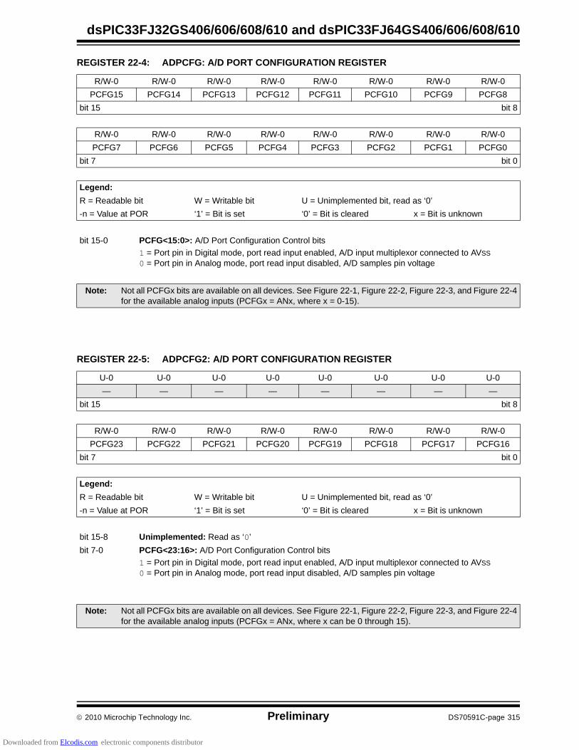
2010 Microchip Technology Inc. Preliminary DS70591C-page 315
dsPIC33FJ32GS406/606/608/610 and dsPIC33FJ64GS406/606/608/610
REGISTER 22-4: ADPCFG: A/D PORT CONFIGURATION REGISTER
R/W-0 R/W-0 R/W-0 R/W-0 R/W-0 R/W-0 R/W-0 R/W-0
PCFG15 PCFG14 PCFG13 PCFG12 PCFG11 PCFG10 PCFG9 PCFG8
bit 15 bit 8
R/W-0 R/W-0 R/W-0 R/W-0 R/W-0 R/W-0 R/W-0 R/W-0
PCFG7 PCFG6 PCFG5 PCFG4 PCFG3 PCFG2 PCFG1 PCFG0
bit 7 bit 0
Legend:
R = Readable bit W = Writable bit U = Unimplemented bit, read as ‘0’
-n = Value at POR ‘1’ = Bit is set ‘0’ = Bit is cleared x = Bit is unknown
bit 15-0 PCFG<15:0>: A/D Port Configuration Control bits
1 = Port pin in Digital mode, port read input enabled, A/D input multiplexor connected to AVSS
0 = Port pin in Analog mode, port read input disabled, A/D samples pin voltage
Note: Not all PCFGx bits are available on all devices. See Figure 22-1, Figure 22-2, Figure 22-3, and Figure 22-4for the available analog inputs (PCFGx = ANx, where x = 0-15).
REGISTER 22-5: ADPCFG2: A/D PORT CONFIGURATION REGISTER
U-0 U-0 U-0 U-0 U-0 U-0 U-0 U-0
— — — — — — — —
bit 15 bit 8
R/W-0 R/W-0 R/W-0 R/W-0 R/W-0 R/W-0 R/W-0 R/W-0
PCFG23 PCFG22 PCFG21 PCFG20 PCFG19 PCFG18 PCFG17 PCFG16
bit 7 bit 0
Legend:
R = Readable bit W = Writable bit U = Unimplemented bit, read as ‘0’
-n = Value at POR ‘1’ = Bit is set ‘0’ = Bit is cleared x = Bit is unknown
bit 15-8 Unimplemented: Read as ‘0’
bit 7-0 PCFG<23:16>: A/D Port Configuration Control bits
1 = Port pin in Digital mode, port read input enabled, A/D input multiplexor connected to AVSS
0 = Port pin in Analog mode, port read input disabled, A/D samples pin voltage
Note: Not all PCFGx bits are available on all devices. See Figure 22-1, Figure 22-2, Figure 22-3, and Figure 22-4for the available analog inputs (PCFGx = ANx, where x can be 0 through 15).
Downloaded from Elcodis.com electronic components distributor
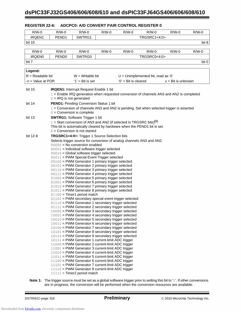
dsPIC33FJ32GS406/606/608/610 and dsPIC33FJ64GS406/606/608/610
DS70591C-page 316 Preliminary 2010 Microchip Technology Inc.
REGISTER 22-6: ADCPC0: A/D CONVERT PAIR CONTROL REGISTER 0
R/W-0 R/W-0 R/W-0 R/W-0 R/W-0 R/W-0 R/W-0 R/W-0
IRQEN1 PEND1 SWTRG1 TRGSRC1<4:0>
bit 15 bit 8
R/W-0 R/W-0 R/W-0 R/W-0 R/W-0 R/W-0 R/W-0 R/W-0
IRQEN0 PEND0 SWTRG0 TRGSRC0<4:0>
bit 7 bit 0
Legend:
R = Readable bit W = Writable bit U = Unimplemented bit, read as ‘0’
-n = Value at POR ‘1’ = Bit is set ‘0’ = Bit is cleared x = Bit is unknown
bit 15 IRQEN1: Interrupt Request Enable 1 bit1 = Enable IRQ generation when requested conversion of channels AN3 and AN2 is completed0 = IRQ is not generated
bit 14 PEND1: Pending Conversion Status 1 bit 1 = Conversion of channels AN3 and AN2 is pending. Set when selected trigger is asserted0 = Conversion is complete
bit 13 SWTRG1: Software Trigger 1 bit1 = Start conversion of AN3 and AN2 (if selected in TRGSRC bits)(1)
This bit is automatically cleared by hardware when the PEND1 bit is set.0 = Conversion is not started
bit 12-8 TRGSRC1<4:0>: Trigger 1 Source Selection bitsSelects trigger source for conversion of analog channels AN3 and AN2.00000 = No conversion enabled00001 = Individual software trigger selected00010 = Global software trigger selected00011 = PWM Special Event Trigger selected00100 = PWM Generator 1 primary trigger selected00101 = PWM Generator 2 primary trigger selected00110 = PWM Generator 3 primary trigger selected00111 = PWM Generator 4 primary trigger selected01000 = PWM Generator 5 primary trigger selected01001 = PWM Generator 6 primary trigger selected01010 = PWM Generator 7 primary trigger selected01011 = PWM Generator 8 primary trigger selected01100 = Timer1 period match01101 = PWM secondary special event trigger selected01110 = PWM Generator 1 secondary trigger selected01111 = PWM Generator 2 secondary trigger selected10000 = PWM Generator 3 secondary trigger selected10001 = PWM Generator 4 secondary trigger selected10010 = PWM Generator 5 secondary trigger selected10011 = PWM Generator 6 secondary trigger selected10100 = PWM Generator 7 secondary trigger selected10101 = PWM Generator 8 secondary trigger selected10110 = PWM Generator 9 secondary trigger selected10111 = PWM Generator 1 current-limit ADC trigger11000 = PWM Generator 2 current-limit ADC trigger11001 = PWM Generator 3 current-limit ADC trigger11010 = PWM Generator 4 current-limit ADC trigger11011 = PWM Generator 5 current-limit ADC trigger11100 = PWM Generator 6 current-limit ADC trigger11101 = PWM Generator 7 current-limit ADC trigger11110 = PWM Generator 8 current-limit ADC trigger11111 = Timer2 period match
Note 1: The trigger source must be set as a global software trigger prior to setting this bit to ‘1’. If other conversionsare in progress, the conversion will be performed when the conversion resources are available.
Downloaded from Elcodis.com electronic components distributor
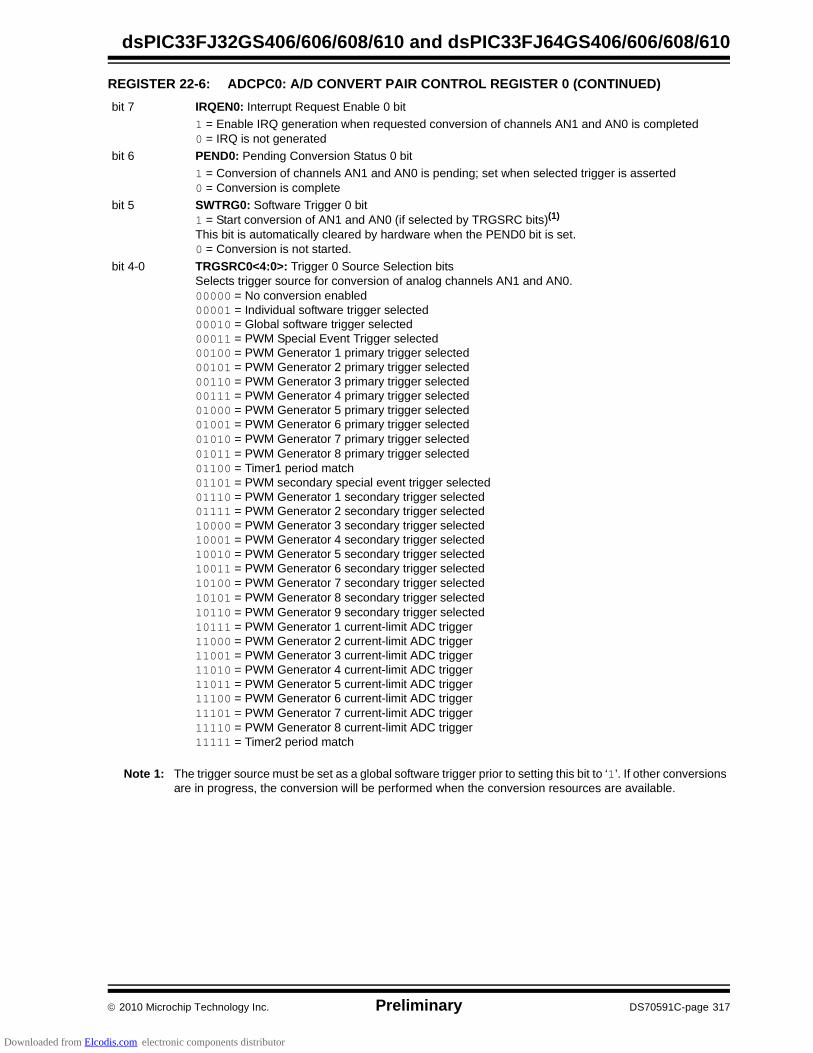
2010 Microchip Technology Inc. Preliminary DS70591C-page 317
dsPIC33FJ32GS406/606/608/610 and dsPIC33FJ64GS406/606/608/610
bit 7 IRQEN0: Interrupt Request Enable 0 bit
1 = Enable IRQ generation when requested conversion of channels AN1 and AN0 is completed0 = IRQ is not generated
bit 6 PEND0: Pending Conversion Status 0 bit
1 = Conversion of channels AN1 and AN0 is pending; set when selected trigger is asserted0 = Conversion is complete
bit 5 SWTRG0: Software Trigger 0 bit1 = Start conversion of AN1 and AN0 (if selected by TRGSRC bits)(1)
This bit is automatically cleared by hardware when the PEND0 bit is set.0 = Conversion is not started.
bit 4-0 TRGSRC0<4:0>: Trigger 0 Source Selection bitsSelects trigger source for conversion of analog channels AN1 and AN0.00000 = No conversion enabled00001 = Individual software trigger selected00010 = Global software trigger selected00011 = PWM Special Event Trigger selected00100 = PWM Generator 1 primary trigger selected00101 = PWM Generator 2 primary trigger selected00110 = PWM Generator 3 primary trigger selected00111 = PWM Generator 4 primary trigger selected01000 = PWM Generator 5 primary trigger selected01001 = PWM Generator 6 primary trigger selected01010 = PWM Generator 7 primary trigger selected01011 = PWM Generator 8 primary trigger selected01100 = Timer1 period match01101 = PWM secondary special event trigger selected01110 = PWM Generator 1 secondary trigger selected01111 = PWM Generator 2 secondary trigger selected10000 = PWM Generator 3 secondary trigger selected10001 = PWM Generator 4 secondary trigger selected10010 = PWM Generator 5 secondary trigger selected10011 = PWM Generator 6 secondary trigger selected10100 = PWM Generator 7 secondary trigger selected10101 = PWM Generator 8 secondary trigger selected10110 = PWM Generator 9 secondary trigger selected10111 = PWM Generator 1 current-limit ADC trigger11000 = PWM Generator 2 current-limit ADC trigger11001 = PWM Generator 3 current-limit ADC trigger11010 = PWM Generator 4 current-limit ADC trigger11011 = PWM Generator 5 current-limit ADC trigger11100 = PWM Generator 6 current-limit ADC trigger11101 = PWM Generator 7 current-limit ADC trigger11110 = PWM Generator 8 current-limit ADC trigger11111 = Timer2 period match
REGISTER 22-6: ADCPC0: A/D CONVERT PAIR CONTROL REGISTER 0 (CONTINUED)
Note 1: The trigger source must be set as a global software trigger prior to setting this bit to ‘1’. If other conversionsare in progress, the conversion will be performed when the conversion resources are available.
Downloaded from Elcodis.com electronic components distributor

dsPIC33FJ32GS406/606/608/610 and dsPIC33FJ64GS406/606/608/610
DS70591C-page 318 Preliminary 2010 Microchip Technology Inc.
REGISTER 22-7: ADCPC1: A/D CONVERT PAIR CONTROL REGISTER 1
R/W-0 R/W-0 R/W-0 R/W-0 R/W-0 R/W-0 R/W-0 R/W-0IRQEN3 PEND3 SWTRG3 TRGSRC3<4:0>
bit 15 bit 8
R/W-0 R/W-0 R/W-0 R/W-0 R/W-0 R/W-0 R/W-0 R/W-0IRQEN2 PEND2 SWTRG2 TRGSRC2<4:0>
bit 7 bit 0
Legend:R = Readable bit W = Writable bit U = Unimplemented bit, read as ‘0’-n = Value at POR ‘1’ = Bit is set ‘0’ = Bit is cleared x = Bit is unknown
bit 15 IRQEN3: Interrupt Request Enable 3 bit
1 = Enable IRQ generation when requested conversion of channels AN7 and AN6 is completed0 = IRQ is not generated
bit 14 PEND3: Pending Conversion Status 3 bit
1 = Conversion of channels AN7 and AN6 is pending. Set when selected trigger is asserted0 = Conversion is complete
bit 13 SWTRG3: Software Trigger 3 bit
1 = Start conversion of AN7 and AN6 (if selected in TRGSRC bits)(1)
This bit is automatically cleared by hardware when the PEND3 bit is set.0 = Conversion is not started.
bit 12-8 TRGSRC3<4:0>: Trigger 3 Source Selection bits(1)
Selects trigger source for conversion of analog channels AN7 and AN6.00000 = No conversion enabled00001 = Individual software trigger selected00010 = Global software trigger selected00011 = PWM Special Event Trigger selected00100 = PWM Generator 1 primary trigger selected00101 = PWM Generator 2 primary trigger selected00110 = PWM Generator 3 primary trigger selected00111 = PWM Generator 4 primary trigger selected01000 = PWM Generator 5 primary trigger selected01001 = PWM Generator 6 primary trigger selected01010 = PWM Generator 7 primary trigger selected01011 = PWM Generator 8 primary trigger selected01100 = Timer1 period match01101 = PWM secondary special event trigger selected01110 = PWM Generator 1 secondary trigger selected01111 = PWM Generator 2 secondary trigger selected10000 = PWM Generator 3 secondary trigger selected10001 = PWM Generator 4 secondary trigger selected10010 = PWM Generator 5 secondary trigger selected10011 = PWM Generator 6 secondary trigger selected10100 = PWM Generator 7 secondary trigger selected10101 = PWM Generator 8 secondary trigger selected10110 = PWM Generator 9 secondary trigger selected10111 = PWM Generator 1 current-limit ADC trigger11000 = PWM Generator 2 current-limit ADC trigger11001 = PWM Generator 3 current-limit ADC trigger11010 = PWM Generator 4 current-limit ADC trigger11011 = PWM Generator 5 current-limit ADC trigger11100 = PWM Generator 6 current-limit ADC trigger11101 = PWM Generator 7 current-limit ADC trigger11110 = PWM Generator 8 current-limit ADC trigger11111 = Timer2 period match
Note 1: The trigger source must be set as a global software trigger prior to setting this bit to ‘1’. If other conversionsare in progress, the conversion will be performed when the conversion resources are available.
Downloaded from Elcodis.com electronic components distributor

2010 Microchip Technology Inc. Preliminary DS70591C-page 319
dsPIC33FJ32GS406/606/608/610 and dsPIC33FJ64GS406/606/608/610
bit 7 IRQEN2: Interrupt Request Enable 2 bit
1 = Enable IRQ generation when requested conversion of channels AN5 and AN4 is completed0 = IRQ is not generated
bit 6 PEND2: Pending Conversion Status 2 bit
1 = Conversion of channels AN5 and AN4 is pending; set when selected trigger is asserted.0 = Conversion is complete
bit 5 SWTRG2: Software Trigger 2 bit
1 = Start conversion of AN5 and AN4 (if selected by TRGSRC bits)(1)
This bit is automatically cleared by hardware when the PEND2 bit is set.0 = Conversion is not started
bit 4-0 TRGSRC2<4:0>: Trigger 2 Source Selection bitsSelects trigger source for conversion of analog channels AN5 and AN4.00000 = No conversion enabled00001 = Individual software trigger selected00010 = Global software trigger selected00011 = PWM Special Event Trigger selected00100 = PWM Generator 1 primary trigger selected00101 = PWM Generator 2 primary trigger selected00110 = PWM Generator 3 primary trigger selected00111 = PWM Generator 4 primary trigger selected01000 = PWM Generator 5 primary trigger selected01001 = PWM Generator 6 primary trigger selected01010 = PWM Generator 7 primary trigger selected01011 = PWM Generator 8 primary trigger selected01100 = Timer1 period match01101 = PWM secondary special event trigger selected01110 = PWM Generator 1 secondary trigger selected01111 = PWM Generator 2 secondary trigger selected10000 = PWM Generator 3 secondary trigger selected10001 = PWM Generator 4 secondary trigger selected10010 = PWM Generator 5 secondary trigger selected10011 = PWM Generator 6 secondary trigger selected10100 = PWM Generator 7 secondary trigger selected10101 = PWM Generator 8 secondary trigger selected10110 = PWM Generator 9 secondary trigger selected10111 = PWM Generator 1 current-limit ADC trigger11000 = PWM Generator 2 current-limit ADC trigger11001 = PWM Generator 3 current-limit ADC trigger11010 = PWM Generator 4 current-limit ADC trigger11011 = PWM Generator 5 current-limit ADC trigger11100 = PWM Generator 6 current-limit ADC trigger11101 = PWM Generator 7 current-limit ADC trigger11110 = PWM Generator 8 current-limit ADC trigger11111 = Timer2 period match
REGISTER 22-7: ADCPC1: A/D CONVERT PAIR CONTROL REGISTER 1 (CONTINUED)
Note 1: The trigger source must be set as a global software trigger prior to setting this bit to ‘1’. If other conversionsare in progress, the conversion will be performed when the conversion resources are available.
Downloaded from Elcodis.com electronic components distributor

dsPIC33FJ32GS406/606/608/610 and dsPIC33FJ64GS406/606/608/610
DS70591C-page 320 Preliminary 2010 Microchip Technology Inc.
REGISTER 22-8: ADCPC2: A/D CONVERT PAIR CONTROL REGISTER 2
R/W-0 R/W-0 R/W-0 R/W-0 R/W-0 R/W-0 R/W-0 R/W-0IRQEN5 PEND5 SWTRG5 TRGSRC5<4:0>
bit 15 bit 8
R/W-0 R/W-0 R/W-0 R/W-0 R/W-0 R/W-0 R/W-0 R/W-0IRQEN4 PEND4 SWTRG4 TRGSRC4<4:0>
bit 7 bit 0
Legend:R = Readable bit W = Writable bit U = Unimplemented bit, read as ‘0’-n = Value at POR ‘1’ = Bit is set ‘0’ = Bit is cleared x = Bit is unknown
bit 15 IRQEN5: Interrupt Request Enable 5 bit1 = Enable IRQ generation when requested conversion of channels AN11 and AN10 is completed0 = IRQ is not generated
bit 14 PEND5: Pending Conversion Status 5 bit 1 = Conversion of channels AN11 and AN10 is pending; set when selected trigger is asserted0 = Conversion is complete
bit 13 SWTRG5: Software Trigger 5 bit1 = Start conversion of AN11 and AN10 (if selected in TRGSRC bits)(1)
This bit is automatically cleared by hardware when the PEND5 bit is set.0 = Conversion is not started
bit 12-8 TRGSRC5<4:0>: Trigger 5 Source Selection bitsSelects trigger source for conversion of analog channels AN11 and AN10.00000 = No conversion enabled00001 = Individual software trigger selected00010 = Global software trigger selected00011 = PWM Special Event Trigger selected00100 = PWM Generator 1 primary trigger selected00101 = PWM Generator 2 primary trigger selected00110 = PWM Generator 3 primary trigger selected00111 = PWM Generator 4 primary trigger selected01000 = PWM Generator 5 primary trigger selected01001 = PWM Generator 6 primary trigger selected01010 = PWM Generator 7 primary trigger selected01011 = PWM Generator 8 primary trigger selected01100 = Timer1 period match01101 = PWM secondary special event trigger selected01110 = PWM Generator 1 secondary trigger selected01111 = PWM Generator 2 secondary trigger selected10000 = PWM Generator 3 secondary trigger selected10001 = PWM Generator 4 secondary trigger selected10010 = PWM Generator 5 secondary trigger selected10011 = PWM Generator 6 secondary trigger selected10100 = PWM Generator 7 secondary trigger selected10101 = PWM Generator 8 secondary trigger selected10110 = PWM Generator 9 secondary trigger selected10111 = PWM Generator 1 current-limit ADC trigger11000 = PWM Generator 2 current-limit ADC trigger11001 = PWM Generator 3 current-limit ADC trigger11010 = PWM Generator 4 current-limit ADC trigger11011 = PWM Generator 5 current-limit ADC trigger11100 = PWM Generator 6 current-limit ADC trigger11101 = PWM Generator 7 current-limit ADC trigger11110 = PWM Generator 8 current-limit ADC trigger11111 = Timer2 period match
Note 1: The trigger source must be set as a global software trigger prior to setting this bit to ‘1’. If other conversionsare in progress, the conversion will be performed when the conversion resources are available.
Downloaded from Elcodis.com electronic components distributor

2010 Microchip Technology Inc. Preliminary DS70591C-page 321
dsPIC33FJ32GS406/606/608/610 and dsPIC33FJ64GS406/606/608/610
bit 7 IRQEN4: Interrupt Request Enable 4 bit
1 = Enable IRQ generation when requested conversion of channels AN9 and AN8 is completed0 = IRQ is not generated
bit 6 PEND4: Pending Conversion Status 4 bit1 = Conversion of channels AN9 and AN8 is pending; set when selected trigger is asserted0 = Conversion is complete
bit 5 SWTRG4: Software Trigger4 bit
1 = Start conversion of AN9 and AN8 (if selected by TRGSRC bits)(1)
This bit is automatically cleared by hardware when the PEND4 bit is set.0 = Conversion is not started
bit 4-0 TRGSRC4<4:0>: Trigger 4 Source Selection bitsSelects trigger source for conversion of analog channels AN9 and AN8.00000 = No conversion enabled00001 = Individual software trigger selected00010 = Global software trigger selected00011 = PWM Special Event Trigger selected00100 = PWM Generator 1 primary trigger selected00101 = PWM Generator 2 primary trigger selected00110 = PWM Generator 3 primary trigger selected00111 = PWM Generator 4 primary trigger selected01000 = PWM Generator 5 primary trigger selected01001 = PWM Generator 6 primary trigger selected01010 = PWM Generator 7 primary trigger selected01011 = PWM Generator 8 primary trigger selected01100 = Timer1 period match01101 = Secondary special event trigger selected01110 = PWM Generator 1 secondary trigger selected01111 = PWM Generator 2 secondary trigger selected10000 = PWM Generator 3 secondary trigger selected10001 = PWM Generator 4 secondary trigger selected10010 = PWM Generator 5 secondary trigger selected10011 = PWM Generator 6 secondary trigger selected10100 = PWM Generator 7 secondary trigger selected10101 = PWM Generator 8 secondary trigger selected10110 = PWM Generator 9 secondary trigger selected10111 = PWM Generator 1 current-limit ADC trigger11000 = PWM Generator 2 current-limit ADC trigger11001 = PWM Generator 3 current-limit ADC trigger11010 = PWM Generator 4 current-limit ADC trigger11011 = PWM Generator 5 current-limit ADC trigger11100 = PWM Generator 6 current-limit ADC trigger11101 = PWM Generator 7 current-limit ADC trigger11110 = PWM Generator 8 current-limit ADC trigger11111 = Timer2 period match
REGISTER 22-8: ADCPC2: A/D CONVERT PAIR CONTROL REGISTER 2 (CONTINUED)
Note 1: The trigger source must be set as a global software trigger prior to setting this bit to ‘1’. If other conversionsare in progress, the conversion will be performed when the conversion resources are available.
Downloaded from Elcodis.com electronic components distributor
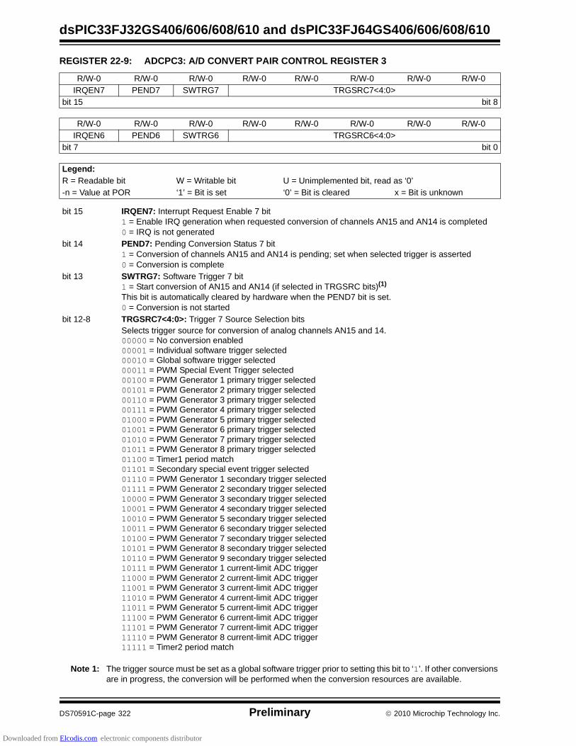
dsPIC33FJ32GS406/606/608/610 and dsPIC33FJ64GS406/606/608/610
DS70591C-page 322 Preliminary 2010 Microchip Technology Inc.
REGISTER 22-9: ADCPC3: A/D CONVERT PAIR CONTROL REGISTER 3
R/W-0 R/W-0 R/W-0 R/W-0 R/W-0 R/W-0 R/W-0 R/W-0IRQEN7 PEND7 SWTRG7 TRGSRC7<4:0>
bit 15 bit 8
R/W-0 R/W-0 R/W-0 R/W-0 R/W-0 R/W-0 R/W-0 R/W-0IRQEN6 PEND6 SWTRG6 TRGSRC6<4:0>
bit 7 bit 0
Legend:R = Readable bit W = Writable bit U = Unimplemented bit, read as ‘0’-n = Value at POR ‘1’ = Bit is set ‘0’ = Bit is cleared x = Bit is unknown
bit 15 IRQEN7: Interrupt Request Enable 7 bit1 = Enable IRQ generation when requested conversion of channels AN15 and AN14 is completed0 = IRQ is not generated
bit 14 PEND7: Pending Conversion Status 7 bit 1 = Conversion of channels AN15 and AN14 is pending; set when selected trigger is asserted0 = Conversion is complete
bit 13 SWTRG7: Software Trigger 7 bit1 = Start conversion of AN15 and AN14 (if selected in TRGSRC bits)(1)
This bit is automatically cleared by hardware when the PEND7 bit is set.0 = Conversion is not started
bit 12-8 TRGSRC7<4:0>: Trigger 7 Source Selection bitsSelects trigger source for conversion of analog channels AN15 and 14.00000 = No conversion enabled00001 = Individual software trigger selected00010 = Global software trigger selected00011 = PWM Special Event Trigger selected00100 = PWM Generator 1 primary trigger selected00101 = PWM Generator 2 primary trigger selected00110 = PWM Generator 3 primary trigger selected00111 = PWM Generator 4 primary trigger selected01000 = PWM Generator 5 primary trigger selected01001 = PWM Generator 6 primary trigger selected01010 = PWM Generator 7 primary trigger selected01011 = PWM Generator 8 primary trigger selected01100 = Timer1 period match01101 = Secondary special event trigger selected01110 = PWM Generator 1 secondary trigger selected01111 = PWM Generator 2 secondary trigger selected10000 = PWM Generator 3 secondary trigger selected10001 = PWM Generator 4 secondary trigger selected10010 = PWM Generator 5 secondary trigger selected10011 = PWM Generator 6 secondary trigger selected10100 = PWM Generator 7 secondary trigger selected10101 = PWM Generator 8 secondary trigger selected10110 = PWM Generator 9 secondary trigger selected10111 = PWM Generator 1 current-limit ADC trigger11000 = PWM Generator 2 current-limit ADC trigger11001 = PWM Generator 3 current-limit ADC trigger11010 = PWM Generator 4 current-limit ADC trigger11011 = PWM Generator 5 current-limit ADC trigger11100 = PWM Generator 6 current-limit ADC trigger11101 = PWM Generator 7 current-limit ADC trigger11110 = PWM Generator 8 current-limit ADC trigger11111 = Timer2 period match
Note 1: The trigger source must be set as a global software trigger prior to setting this bit to ‘1’. If other conversionsare in progress, the conversion will be performed when the conversion resources are available.
Downloaded from Elcodis.com electronic components distributor

2010 Microchip Technology Inc. Preliminary DS70591C-page 323
dsPIC33FJ32GS406/606/608/610 and dsPIC33FJ64GS406/606/608/610
bit 7 IRQEN6: Interrupt Request Enable 6 bit
1 = Enable IRQ generation when requested conversion of channels AN13 and AN12 is completed0 = IRQ is not generated
bit 6 PEND6: Pending Conversion Status 6 bit1 = Conversion of channels AN13 and AN12 is pending; set when selected trigger is asserted0 = Conversion is complete
bit 5 SWTRG6: Software Trigger 6 bit
1 = Start conversion of AN13 and AN12 (if selected by TRGSRC bits)(1)
This bit is automatically cleared by hardware when the PEND6 bit is set.0 = Conversion is not started
bit 4-0 TRGSRC6<4:0>: Trigger 6 Source Selection bitsSelects trigger source for conversion of analog channels AN13 and AN12.00000 = No conversion enabled00001 = Individual software trigger selected00010 = Global software trigger selected00011 = PWM Special Event Trigger selected00100 = PWM Generator 1 primary trigger selected00101 = PWM Generator 2 primary trigger selected00110 = PWM Generator 3 primary trigger selected00111 = PWM Generator 4 primary trigger selected01000 = PWM Generator 5 primary trigger selected01001 = PWM Generator 6 primary trigger selected01010 = PWM Generator 7 primary trigger selected01011 = PWM Generator 8 primary trigger selected01100 = Timer1 period match01101 = Secondary special event trigger selected01110 = PWM Generator 1 secondary trigger selected01111 = PWM Generator 2 secondary trigger selected10000 = PWM Generator 3 secondary trigger selected10001 = PWM Generator 4 secondary trigger selected10010 = PWM Generator 5 secondary trigger selected10011 = PWM Generator 6 secondary trigger selected10100 = PWM Generator 7 secondary trigger selected10101 = PWM Generator 8 secondary trigger selected10110 = PWM Generator 9 secondary trigger selected10111 = PWM Generator 1 current-limit ADC trigger11000 = PWM Generator 2 current-limit ADC trigger11001 = PWM Generator 3 current-limit ADC trigger11010 = PWM Generator 4 current-limit ADC trigger11011 = PWM Generator 5 current-limit ADC trigger11100 = PWM Generator 6 current-limit ADC trigger11101 = PWM Generator 7 current-limit ADC trigger11110 = PWM Generator 8 current-limit ADC trigger11111 = Timer2 period match
REGISTER 22-9: ADCPC3: A/D CONVERT PAIR CONTROL REGISTER 3 (CONTINUED)
Note 1: The trigger source must be set as a global software trigger prior to setting this bit to ‘1’. If other conversionsare in progress, the conversion will be performed when the conversion resources are available.
Downloaded from Elcodis.com electronic components distributor

dsPIC33FJ32GS406/606/608/610 and dsPIC33FJ64GS406/606/608/610
DS70591C-page 324 Preliminary 2010 Microchip Technology Inc.
REGISTER 22-10: ADCPC4: A/D CONVERT PAIR CONTROL REGISTER 4
R/W-0 R/W-0 R/W-0 R/W-0 R/W-0 R/W-0 R/W-0 R/W-0IRQEN9 PEND9 SWTRG9 TRGSRC9<4:0>
bit 15 bit 8
R/W-0 R/W-0 R/W-0 R/W-0 R/W-0 R/W-0 R/W-0 R/W-0IRQEN8 PEND8 SWTRG8 TRGSRC8<4:0>
bit 7 bit 0
Legend:R = Readable bit W = Writable bit U = Unimplemented bit, read as ‘0’-n = Value at POR ‘1’ = Bit is set ‘0’ = Bit is cleared x = Bit is unknown
bit 15 IRQEN9: Interrupt Request Enable 9 bit1 = Enable IRQ generation when requested conversion of channels AN19 and AN18 is completed0 = IRQ is not generated
bit 14 PEND9: Pending Conversion Status 9 bit 1 = Conversion of channels AN19 and AN18 is pending; set when selected trigger is asserted0 = Conversion is complete
bit 13 SWTRG9: Software Trigger 9 bit1 = Start conversion of AN19 and AN18 (if selected in TRGSRC bits)(1)
This bit is automatically cleared by hardware when the PEND9 bit is set.0 = Conversion is not started
bit 12-8 TRGSRC9<4:0>: Trigger 9 Source Selection bitsSelects trigger source for conversion of analog channels AN19 and AN18.00000 = No conversion enabled00001 = Individual software trigger selected00010 = Global software trigger selected00011 = PWM Special Event Trigger selected00100 = PWM Generator 1 primary trigger selected00101 = PWM Generator 2 primary trigger selected00110 = PWM Generator 3 primary trigger selected00111 = PWM Generator 4 primary trigger selected01000 = PWM Generator 5 primary trigger selected01001 = PWM Generator 6 primary trigger selected01010 = PWM Generator 7 primary trigger selected01011 = PWM Generator 8 primary trigger selected01100 = Timer1 period match01101 = PWM secondary special event trigger selected01110 = PWM Generator 1 secondary trigger selected01111 = PWM Generator 2 secondary trigger selected10000 = PWM Generator 3 secondary trigger selected10001 = PWM Generator 4 secondary trigger selected10010 = PWM Generator 5 secondary trigger selected10011 = PWM Generator 6 secondary trigger selected10100 = PWM Generator 7 secondary trigger selected10101 = PWM Generator 8 secondary trigger selected10110 = PWM Generator 9 secondary trigger selected10111 = PWM Generator 1 current-limit ADC trigger11000 = PWM Generator 2 current-limit ADC trigger11001 = PWM Generator 3 current-limit ADC trigger11010 = PWM Generator 4 current-limit ADC trigger11011 = PWM Generator 5 current-limit ADC trigger11100 = PWM Generator 6 current-limit ADC trigger11101 = PWM Generator 7 current-limit ADC trigger11110 = PWM Generator 8 current-limit ADC trigger11111 = Timer2 period match
Note 1: The trigger source must be set as a global software trigger prior to setting this bit to ‘1’. If other conversionsare in progress, the conversion will be performed when the conversion resources are available.
Downloaded from Elcodis.com electronic components distributor

2010 Microchip Technology Inc. Preliminary DS70591C-page 325
dsPIC33FJ32GS406/606/608/610 and dsPIC33FJ64GS406/606/608/610
bit 7 IRQEN8: Interrupt Request Enable 8 bit
1 = Enable IRQ generation when requested conversion of channels AN17 and AN16 is completed0 = IRQ is not generated
bit 6 PEND8: Pending Conversion Status 8 bit1 = Conversion of channels AN17 and AN16 is pending; set when selected trigger is asserted0 = Conversion is complete
bit 5 SWTRG8: Software Trigger 8 bit
1 = Start conversion of AN17 and AN16 (if selected by TRGSRC bits)(1)
This bit is automatically cleared by hardware when the PEND8 bit is set.0 = Conversion is not started
bit 4-0 TRGSRC8<4:0>: Trigger 8 Source Selection bitsSelects trigger source for conversion of analog channels AN17 and AN16.00000 = No conversion enabled00001 = Individual software trigger selected00010 = Global software trigger selected00011 = PWM Special Event Trigger selected00100 = PWM Generator 1 primary trigger selected00101 = PWM Generator 2 primary trigger selected00110 = PWM Generator 3 primary trigger selected00111 = PWM Generator 4 primary trigger selected01000 = PWM Generator 5 primary trigger selected01001 = PWM Generator 6 primary trigger selected01010 = PWM Generator 7 primary trigger selected01011 = PWM Generator 8 primary trigger selected01100 = Timer1 period match01101 = PWM secondary special event trigger selected01110 = PWM Generator 1 secondary trigger selected01111 = PWM Generator 2 secondary trigger selected10000 = PWM Generator 3 secondary trigger selected10001 = PWM Generator 4 secondary trigger selected10010 = PWM Generator 5 secondary trigger selected10011 = PWM Generator 6 secondary trigger selected10100 = PWM Generator 7 secondary trigger selected10101 = PWM Generator 8 secondary trigger selected10110 = PWM Generator 9 secondary trigger selected10111 = PWM Generator 1 current-limit ADC trigger11000 = PWM Generator 2 current-limit ADC trigger11001 = PWM Generator 3 current-limit ADC trigger11010 = PWM Generator 4 current-limit ADC trigger11011 = PWM Generator 5 current-limit ADC trigger11100 = PWM Generator 6 current-limit ADC trigger11101 = PWM Generator 7 current-limit ADC trigger11110 = PWM Generator 8 current-limit ADC trigger11111 = Timer2 period match
REGISTER 22-10: ADCPC4: A/D CONVERT PAIR CONTROL REGISTER 4 (CONTINUED)
Note 1: The trigger source must be set as a global software trigger prior to setting this bit to ‘1’. If other conversionsare in progress, the conversion will be performed when the conversion resources are available.
Downloaded from Elcodis.com electronic components distributor

dsPIC33FJ32GS406/606/608/610 and dsPIC33FJ64GS406/606/608/610
DS70591C-page 326 Preliminary 2010 Microchip Technology Inc.
REGISTER 22-11: ADCPC5: A/D CONVERT PAIR CONTROL REGISTER 5
R/W-0 R/W-0 R/W-0 R/W-0 R/W-0 R/W-0 R/W-0 R/W-0IRQEN11 PEND11 SWTRG11 TRGSRC11<4:0>
bit 15 bit 8
R/W-0 R/W-0 R/W-0 R/W-0 R/W-0 R/W-0 R/W-0 R/W-0IRQEN10 PEND10 SWTRG10 TRGSRC10<4:0>
bit 7 bit 0
Legend:R = Readable bit W = Writable bit U = Unimplemented bit, read as ‘0’-n = Value at POR ‘1’ = Bit is set ‘0’ = Bit is cleared x = Bit is unknown
bit 15 IRQEN11: Interrupt Request Enable 11 bit1 = Enable IRQ generation when requested conversion of channels AN23 and AN22 is completed0 = IRQ is not generated
bit 14 PEND11: Pending Conversion Status 11 bit 1 = Conversion of channels AN23 and AN22 is pending; set when selected trigger is asserted0 = Conversion is complete
bit 13 SWTRG11: Software Trigger 11 bit1 = Start conversion of AN23 and AN22 (if selected in TRGSRC bits)(1). This bit is automatically
cleared by hardware when the PEND11 bit is set.0 = Conversion is not started
bit 12-8 TRGSRC11<4:0>: Trigger 11 Source Selection bitsSelects trigger source for conversion of analog channels AN23 and AN22.00000 = No conversion enabled00001 = Individual software trigger selected00010 = Global software trigger selected00011 = PWM Special Event Trigger selected00100 = PWM Generator 1 primary trigger selected00101 = PWM Generator 2 primary trigger selected00110 = PWM Generator 3 primary trigger selected00111 = PWM Generator 4 primary trigger selected01000 = PWM Generator 5 primary trigger selected01001 = PWM Generator 6 primary trigger selected01010 = PWM Generator 7 primary trigger selected01011 = PWM Generator 8 primary trigger selected01100 = Timer1 period match01101 = PWM secondary special event trigger selected01110 = PWM Generator 1 secondary trigger selected01111 = PWM Generator 2 secondary trigger selected10000 = PWM Generator 3 secondary trigger selected10001 = PWM Generator 4 secondary trigger selected10010 = PWM Generator 5 secondary trigger selected10011 = PWM Generator 6 secondary trigger selected10100 = PWM Generator 7 secondary trigger selected10101 = PWM Generator 8 secondary trigger selected10110 = PWM Generator 9 secondary trigger selected10111 = PWM Generator 1 current-limit ADC trigger11000 = PWM Generator 2 current-limit ADC trigger11001 = PWM Generator 3 current-limit ADC trigger11010 = PWM Generator 4 current-limit ADC trigger11011 = PWM Generator 5 current-limit ADC trigger11100 = PWM Generator 6 current-limit ADC trigger11101 = PWM Generator 7 current-limit ADC trigger11110 = PWM Generator 8 current-limit ADC trigger11111 = Timer2 period match
Note 1: The trigger source must be set as a global software trigger prior to setting this bit to ‘1’. If other conversionsare in progress, the conversion will be performed when the conversion resources are available.
Downloaded from Elcodis.com electronic components distributor

2010 Microchip Technology Inc. Preliminary DS70591C-page 327
dsPIC33FJ32GS406/606/608/610 and dsPIC33FJ64GS406/606/608/610
bit 7 IRQEN10: Interrupt Request Enable 10 bit1 = Enable IRQ generation when requested conversion of channels AN21 and AN20 is completed0 = IRQ is not generated
bit 6 PEND10: Pending Conversion Status 10 bit1 = Conversion of channels AN21 and AN20 is pending; set when selected trigger is asserted0 = Conversion is complete
bit 5 SWTRG10: Software Trigger 10 bit
1 = Start conversion of AN21 and AN20 (if selected by TRGSRC bits)(1). This bit is automaticallycleared by hardware when the PEND10 bit is set.
0 = Conversion is not startedbit 4-0 TRGSRC10<4:0>: Trigger 10 Source Selection bits
Selects trigger source for conversion of analog channels AN21 and AN20.00000 = No conversion enabled00001 = Individual software trigger selected00010 = Global software trigger selected00011 = PWM Special Event Trigger selected00100 = PWM Generator 1 primary trigger selected00101 = PWM Generator 2 primary trigger selected00110 = PWM Generator 3 primary trigger selected00111 = PWM Generator 4 primary trigger selected01000 = PWM Generator 5 primary trigger selected01001 = PWM Generator 6 primary trigger selected01010 = PWM Generator 7 primary trigger selected01011 = PWM Generator 8 primary trigger selected01100 = Timer1 period match01101 = PWM secondary special event trigger selected01110 = PWM Generator 1 secondary trigger selected01111 = PWM Generator 2 secondary trigger selected10000 = PWM Generator 3 secondary trigger selected10001 = PWM Generator 4 secondary trigger selected10010 = PWM Generator 5 secondary trigger selected10011 = PWM Generator 6 secondary trigger selected10100 = PWM Generator 7 secondary trigger selected10101 = PWM Generator 8 secondary trigger selected10110 = PWM Generator 9 secondary trigger selected10111 = PWM Generator 1 current-limit ADC trigger11000 = PWM Generator 2 current-limit ADC trigger11001 = PWM Generator 3 current-limit ADC trigger11010 = PWM Generator 4 current-limit ADC trigger11011 = PWM Generator 5 current-limit ADC trigger11100 = PWM Generator 6 current-limit ADC trigger11101 = PWM Generator 7 current-limit ADC trigger11110 = PWM Generator 8 current-limit ADC trigger11111 = Timer2 period match
REGISTER 22-11: ADCPC5: A/D CONVERT PAIR CONTROL REGISTER 5 (CONTINUED)
Note 1: The trigger source must be set as a global software trigger prior to setting this bit to ‘1’. If other conversionsare in progress, the conversion will be performed when the conversion resources are available.
Downloaded from Elcodis.com electronic components distributor

dsPIC33FJ32GS406/606/608/610 and dsPIC33FJ64GS406/606/608/610
DS70591C-page 328 Preliminary 2010 Microchip Technology Inc.
REGISTER 22-12: ADCPC6: A/D CONVERT PAIR CONTROL REGISTER 6
U-0 U-0 U-0 U-0 U-0 U-0 U-0 U-0
— — — — — — — —bit 15 bit 8
R/W-0 R/W-0 R/W-0 R/W-0 R/W-0 R/W-0 R/W-0 R/W-0IRQEN12 PEND12 SWTRG12 TRGSRC12<4:0>
bit 7 bit 0
Legend:R = Readable bit W = Writable bit U = Unimplemented bit, read as ‘0’-n = Value at POR ‘1’ = Bit is set ‘0’ = Bit is cleared x = Bit is unknown
bit 15-8 Unimplemented: Read as ‘0’bit 7 IRQEN12: Interrupt Request Enable 12 bit
1 = Enable IRQ generation when requested conversion of channels AN25 and AN24 is completed0 = IRQ is not generated
bit 6 PEND12: Pending Conversion Status 12 bit1 = Conversion of channels AN25 and AN24 is pending; set when selected trigger is asserted0 = Conversion is complete
bit 5 SWTRG12: Software Trigger 12 bit1 = Start conversion of AN25 (INTREF) and AN24 (EXTREF) if selected by TRGSRC bits(1)
This bit is automatically cleared by hardware when the PEND12 bit is set.0 = Conversion is not started.
bit 4-0 TRGSRC12<4:0>: Trigger 12 Source Selection bitsSelects trigger source for conversion of analog channels AN25 and AN24.00000 = No conversion enabled00001 = Individual software trigger selected00010 = Global software trigger selected00011 = PWM Special Event Trigger selected00100 = PWM Generator 1 primary trigger selected00101 = PWM Generator 2 primary trigger selected00110 = PWM Generator 3 primary trigger selected00111 = PWM Generator 4 primary trigger selected01000 = PWM Generator 5 primary trigger selected01001 = PWM Generator 6 primary trigger selected01010 = PWM Generator 7 primary trigger selected01011 = PWM Generator 8 primary trigger selected01100 = Timer1 period match01101 = PWM secondary special event trigger selected01110 = PWM Generator 1 secondary trigger selected01111 = PWM Generator 2 secondary trigger selected10000 = PWM Generator 3 secondary trigger selected10001 = PWM Generator 4 secondary trigger selected10010 = PWM Generator 5 secondary trigger selected10011 = PWM Generator 6 secondary trigger selected10100 = PWM Generator 7 secondary trigger selected10101 = PWM Generator 8 secondary trigger selected10110 = PWM Generator 9 secondary trigger selected10111 = PWM Generator 1 current-limit ADC trigger11000 = PWM Generator 2 current-limit ADC trigger11001 = PWM Generator 3 current-limit ADC trigger11010 = PWM Generator 4 current-limit ADC trigger11011 = PWM Generator 5 current-limit ADC trigger11100 = PWM Generator 6 current-limit ADC trigger11101 = PWM Generator 7 current-limit ADC trigger11110 = PWM Generator 8 current-limit ADC trigger11111 = Timer2 period match
Note 1: The trigger source must be set as a global software trigger prior to setting this bit to ‘1’. If other conversionsare in progress, the conversion will be performed when the conversion resources are available.
Downloaded from Elcodis.com electronic components distributor
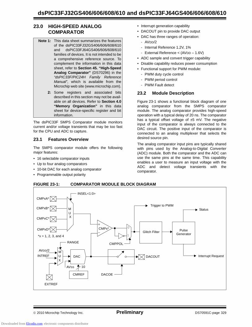
2010 Microchip Technology Inc. Preliminary DS70591C-page 329
dsPIC33FJ32GS406/606/608/610 and dsPIC33FJ64GS406/606/608/610
23.0 HIGH-SPEED ANALOG COMPARATOR
The dsPIC33F SMPS Comparator module monitorscurrent and/or voltage transients that may be too fastfor the CPU and ADC to capture.
23.1 Features Overview
The SMPS comparator module offers the followingmajor features:
• 16 selectable comparator inputs
• Up to four analog comparators
• 10-bit DAC for each analog comparator
• Programmable output polarity
• Interrupt generation capability
• DACOUT pin to provide DAC output
• DAC has three ranges of operation:
- AVDD/2
- Internal Reference 1.2V, 1%
- External Reference < (AVDD – 1.6V)
• ADC sample and convert trigger capability
• Disable capability reduces power consumption
• Functional support for PWM module:
- PWM duty cycle control
- PWM period control
- PWM Fault detect
23.2 Module Description
Figure 23-1 shows a functional block diagram of oneanalog comparator from the SMPS comparatormodule. The analog comparator provides high-speedoperation with a typical delay of 20 ns. The comparatorhas a typical offset voltage of ±5 mV. The negativeinput of the comparator is always connected to theDAC circuit. The positive input of the comparator isconnected to an analog multiplexer that selects thedesired source pin.
The analog comparator input pins are typically sharedwith pins used by the Analog-to-Digital Converter(ADC) module. Both the comparator and the ADC canuse the same pins at the same time. This capabilityenables a user to measure an input voltage with theADC and detect voltage transients with thecomparator.
FIGURE 23-1: COMPARATOR MODULE BLOCK DIAGRAM
Note 1: This data sheet summarizes the featuresof the dsPIC33FJ32GS406/606/608/610and dsPIC33FJ64GS406/606/608/610families of devices. It is not intended to bea comprehensive reference source. Tocomplement the information in this datasheet, refer to Section 45. “High-SpeedAnalog Comparator” (DS70296) in the“dsPIC33F/PIC24H Family ReferenceManual”, which is available from theMicrochip web site (www.microchip.com).
2: Some registers and associated bitsdescribed in this section may not be avail-able on all devices. Refer to Section 4.0“Memory Organization” in this datasheet for device-specific register and bitinformation.
CMPxA*
CMPxC*
DAC
CMPPOL
0
1
AVDD/2
INTREF
MUX
MUX
CMREF
CMPx*
INSEL<1:0>
10
Trigger to PWM
Interrupt Request
CMPxB*
CMPxD*Glitch Filter Pulse
EXTREF
Status
AVSS
Generator *x = 1, 2, 3, and 4
RANGE
DACOUT
DACOE
Downloaded from Elcodis.com electronic components distributor

dsPIC33FJ32GS406/606/608/610 and dsPIC33FJ64GS406/606/608/610
DS70591C-page 330 Preliminary 2010 Microchip Technology Inc.
23.3 Module Applications
This module provides a means for the SMPS dsPICDSC devices to monitor voltage and currents in apower conversion application. The ability to detecttransient conditions and stimulate the dsPIC DSCprocessor and/or peripherals, without requiring theprocessor and ADC to constantly monitor voltages orcurrents, frees the dsPIC DSC to perform other tasks.
The comparator module has a high-speed comparatorand an associated 10-bit DAC that provides aprogrammable reference voltage to the inverting inputof the comparator. The polarity of the comparator out-put is user-programmable. The output of the modulecan be used in the following modes:
• Generate an Interrupt
• Trigger an ADC Sample and Convert Process
• Truncate the PWM Signal (current limit)
• Truncate the PWM Period (current minimum)
• Disable the PWM Outputs (Fault latch)
The output of the comparator module may be used inmultiple modes at the same time, such as: (1)generate an interrupt, (2) have the ADC take a sampleand convert it, and (3) truncate the PWM output inresponse to a voltage being detected beyond itsexpected value.
The comparator module can also be used to wake-upthe system from Sleep or Idle mode when the analoginput voltage exceeds the programmed thresholdvoltage.
23.4 DAC
The range of the DAC is controlled via an analogmultiplexer that selects either AVDD/2, internal 1.2V,1% reference, or an external reference source,EXTREF. The full range of the DAC (AVDD/2) willtypically be used when the chosen input source pin isshared with the ADC. The reduced range option(INTREF) will likely be used when monitoring currentlevels using a current sense resistor. Usually, themeasured voltages in such applications are small(<1.25V); therefore the option of using a reducedreference range for the comparator extends theavailable DAC resolution in these applications. Theuse of an external reference enables the user toconnect to a reference that better suits theirapplication.
DACOUT, shown in Figure 23-1, can only beassociated with a single comparator at a given time.
23.5 Interaction with I/O Buffers
If the comparator module is enabled and a pin hasbeen selected as the source for the comparator, thenthe chosen I/O pad must disable the digital input bufferassociated with the pad to prevent excessive currentsin the digital buffer due to analog input voltages.
23.6 Digital Logic
The CMPCONx register (see Register 23-1) providesthe control logic that configures the comparatormodule. The digital logic provides a glitch filter for thecomparator output to mask transient signals in lessthan two instruction cycles. In Sleep or Idle mode, theglitch filter is bypassed to enable an asynchronouspath from the comparator to the interrupt controller.This asynchronous path can be used to wake-up theprocessor from Sleep or Idle mode.
The comparator can be disabled while in Idle mode ifthe CMPSIDL bit is set. If a device has multiplecomparators, if any CMPSIDL bit is set, then the entiregroup of comparators will be disabled while in Idlemode. This behavior reduces complexity in the designof the clock control logic for this module.
The digital logic also provides a one TCY width pulsegenerator for triggering the ADC and generatinginterrupt requests.
The CMPDACx (see Register 23-2) register providesthe digital input value to the reference DAC.
If the module is disabled, the DAC and comparator aredisabled to reduce power consumption.
23.7 Comparator Input Range
The comparator has a limitation for the input CommonMode Range (CMR) of (AVDD – 1.5V), typical. Thismeans that both inputs should not exceed this range.As long as one of the inputs is within the CommonMode Range, the comparator output will be correct.However, any input exceeding the CMR limitation willcause the comparator input to be saturated.
If both inputs exceed the CMR, the comparator outputwill be indeterminate.
23.8 DAC Output Range
The DAC has a limitation for the maximum referencevoltage input of (AVDD – 1.6) volts. An externalreference voltage input should not exceed this value orthe reference DAC output will become indeterminate.
23.9 Comparator Registers
The comparator module is controlled by the followingregisters:
• CMPCONx: Comparator Control Register• CMPDACx: Comparator DAC Control Register
Note: It should be ensured in software thatmultiple DACOE bits are not set. Theoutput on the DACOUT pin will be indeter-minate if multiple comparators enable theDAC output.
Downloaded from Elcodis.com electronic components distributor
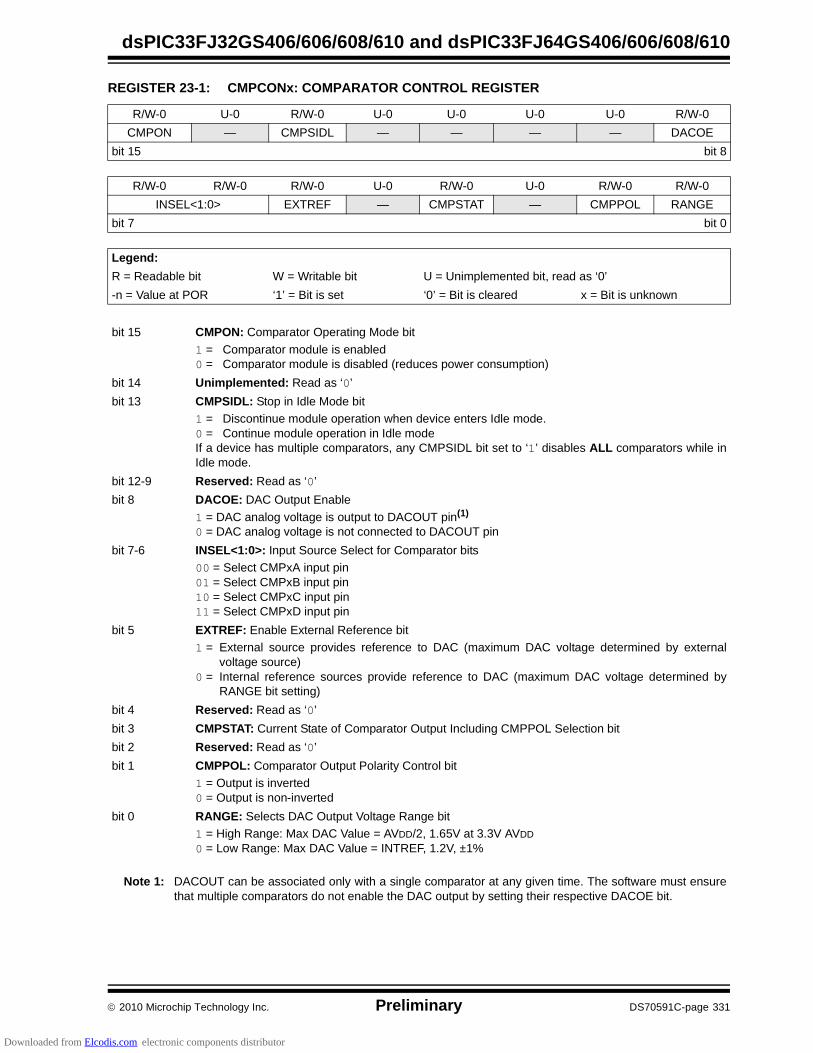
2010 Microchip Technology Inc. Preliminary DS70591C-page 331
dsPIC33FJ32GS406/606/608/610 and dsPIC33FJ64GS406/606/608/610
REGISTER 23-1: CMPCONx: COMPARATOR CONTROL REGISTER
R/W-0 U-0 R/W-0 U-0 U-0 U-0 U-0 R/W-0
CMPON — CMPSIDL — — — — DACOE
bit 15 bit 8
R/W-0 R/W-0 R/W-0 U-0 R/W-0 U-0 R/W-0 R/W-0
INSEL<1:0> EXTREF — CMPSTAT — CMPPOL RANGE
bit 7 bit 0
Legend:
R = Readable bit W = Writable bit U = Unimplemented bit, read as ‘0’
-n = Value at POR ‘1’ = Bit is set ‘0’ = Bit is cleared x = Bit is unknown
bit 15 CMPON: Comparator Operating Mode bit
1 = Comparator module is enabled0 = Comparator module is disabled (reduces power consumption)
bit 14 Unimplemented: Read as ‘0’
bit 13 CMPSIDL: Stop in Idle Mode bit
1 = Discontinue module operation when device enters Idle mode.0 = Continue module operation in Idle modeIf a device has multiple comparators, any CMPSIDL bit set to ‘1’ disables ALL comparators while inIdle mode.
bit 12-9 Reserved: Read as ‘0’
bit 8 DACOE: DAC Output Enable
1 = DAC analog voltage is output to DACOUT pin(1)
0 = DAC analog voltage is not connected to DACOUT pin
bit 7-6 INSEL<1:0>: Input Source Select for Comparator bits
00 = Select CMPxA input pin01 = Select CMPxB input pin10 = Select CMPxC input pin11 = Select CMPxD input pin
bit 5 EXTREF: Enable External Reference bit
1 = External source provides reference to DAC (maximum DAC voltage determined by externalvoltage source)
0 = Internal reference sources provide reference to DAC (maximum DAC voltage determined byRANGE bit setting)
bit 4 Reserved: Read as ‘0’
bit 3 CMPSTAT: Current State of Comparator Output Including CMPPOL Selection bit
bit 2 Reserved: Read as ‘0’
bit 1 CMPPOL: Comparator Output Polarity Control bit
1 = Output is inverted0 = Output is non-inverted
bit 0 RANGE: Selects DAC Output Voltage Range bit
1 = High Range: Max DAC Value = AVDD/2, 1.65V at 3.3V AVDD
0 = Low Range: Max DAC Value = INTREF, 1.2V, ±1%
Note 1: DACOUT can be associated only with a single comparator at any given time. The software must ensurethat multiple comparators do not enable the DAC output by setting their respective DACOE bit.
Downloaded from Elcodis.com electronic components distributor

dsPIC33FJ32GS406/606/608/610 and dsPIC33FJ64GS406/606/608/610
DS70591C-page 332 Preliminary 2010 Microchip Technology Inc.
REGISTER 23-2: CMPDACx: COMPARATOR DAC CONTROL REGISTER
U-0 U-0 U-0 U-0 U-0 U-0 R/W-0 R/W-0
— — — — — — CMREF<9:8>
bit 15 bit 8
R/W-0 R/W-0 R/W-0 R/W-0 R/W-0 R/W-0 R/W-0 R/W-0
CMREF<7:0>
bit 7 bit 0
Legend:
R = Readable bit W = Writable bit U = Unimplemented bit, read as ‘0’
-n = Value at POR ‘1’ = Bit is set ‘0’ = Bit is cleared x = Bit is unknown
bit 15-10 Reserved: Read as ‘0’
bit 9-0 CMREF<9:0>: Comparator Reference Voltage Select bits
1111111111 = (CMREF * INTREF/1024) or (CMREF * (AVDD/2)/1024) volts depending on RANGEbit or (CMREF * EXTREF/1024) if EXTREF is set
•
•
•
0000000000 = 0.0 volts
Downloaded from Elcodis.com electronic components distributor
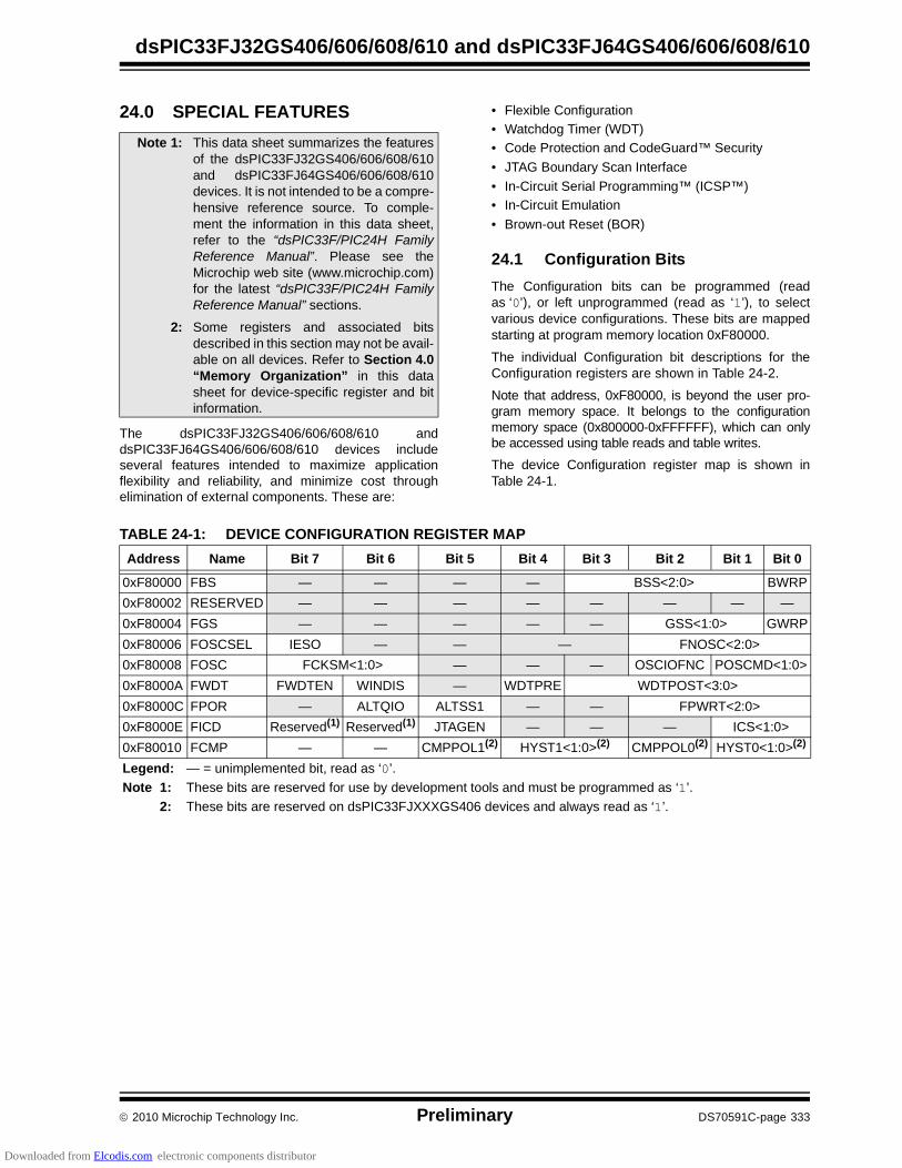
2010 Microchip Technology Inc. Preliminary DS70591C-page 333
dsPIC33FJ32GS406/606/608/610 and dsPIC33FJ64GS406/606/608/610
24.0 SPECIAL FEATURES
The dsPIC33FJ32GS406/606/608/610 anddsPIC33FJ64GS406/606/608/610 devices includeseveral features intended to maximize applicationflexibility and reliability, and minimize cost throughelimination of external components. These are:
• Flexible Configuration
• Watchdog Timer (WDT)
• Code Protection and CodeGuard™ Security
• JTAG Boundary Scan Interface
• In-Circuit Serial Programming™ (ICSP™)
• In-Circuit Emulation
• Brown-out Reset (BOR)
24.1 Configuration Bits
The Configuration bits can be programmed (readas ‘0’), or left unprogrammed (read as ‘1’), to selectvarious device configurations. These bits are mappedstarting at program memory location 0xF80000.
The individual Configuration bit descriptions for theConfiguration registers are shown in Table 24-2.
Note that address, 0xF80000, is beyond the user pro-gram memory space. It belongs to the configurationmemory space (0x800000-0xFFFFFF), which can onlybe accessed using table reads and table writes.
The device Configuration register map is shown inTable 24-1.
Note 1: This data sheet summarizes the featuresof the dsPIC33FJ32GS406/606/608/610and dsPIC33FJ64GS406/606/608/610devices. It is not intended to be a compre-hensive reference source. To comple-ment the information in this data sheet,refer to the “dsPIC33F/PIC24H FamilyReference Manual”. Please see theMicrochip web site (www.microchip.com)for the latest “dsPIC33F/PIC24H FamilyReference Manual” sections.
2: Some registers and associated bitsdescribed in this section may not be avail-able on all devices. Refer to Section 4.0“Memory Organization” in this datasheet for device-specific register and bitinformation.
TABLE 24-1: DEVICE CONFIGURATION REGISTER MAP
Address Name Bit 7 Bit 6 Bit 5 Bit 4 Bit 3 Bit 2 Bit 1 Bit 0
0xF80000 FBS — — — — BSS<2:0> BWRP
0xF80002 RESERVED — — — — — — — —
0xF80004 FGS — — — — — GSS<1:0> GWRP
0xF80006 FOSCSEL IESO — — — FNOSC<2:0>
0xF80008 FOSC FCKSM<1:0> — — — OSCIOFNC POSCMD<1:0>
0xF8000A FWDT FWDTEN WINDIS — WDTPRE WDTPOST<3:0>
0xF8000C FPOR — ALTQIO ALTSS1 — — FPWRT<2:0>
0xF8000E FICD Reserved(1) Reserved(1) JTAGEN — — — ICS<1:0>
0xF80010 FCMP — — CMPPOL1(2) HYST1<1:0>(2) CMPPOL0(2) HYST0<1:0>(2)
Legend: — = unimplemented bit, read as ‘0’.
Note 1: These bits are reserved for use by development tools and must be programmed as ‘1’.
2: These bits are reserved on dsPIC33FJXXXGS406 devices and always read as ‘1’.
Downloaded from Elcodis.com electronic components distributor
dsPIC33FJ32GS406/606/608/610 and dsPIC33FJ64GS406/606/608/610
DS70591C-page 334 Preliminary 2010 Microchip Technology Inc.
TABLE 24-2: dsPIC33F CONFIGURATION BITS DESCRIPTION
Bit Field Register Description
BWRP FBS Boot Segment Program Flash Write Protection bit1 = Boot segment can be written0 = Boot segment is write-protected
BSS<2:0> FBS Boot Segment Program Flash Code Protection Size bitsX11 = No boot program Flash segment
Boot space is 256 instruction words (except interrupt vectors)110 = Standard security; boot program Flash segment ends at
0x0003FE010 = High security; boot program Flash segment ends at 0x0003FE
Boot space is 768 instruction words (except interrupt vectors)101 = Standard security; boot program Flash segment ends at
0x0007FE001 = High security; boot program Flash segment ends at 0x0007FE
Boot space is 1792 instruction words (except interrupt vectors)100 = Standard security; boot program Flash segment ends at
0x000FFE000 = High security; boot program Flash segment ends at 0x000FFE
GSS<1:0> FGS General Segment Code-Protect bits11 = User program memory is not code-protected10 = Standard security0x = High security
GWRP FGS General Segment Write-Protect bit1 = User program memory is not write-protected0 = User program memory is write-protected
IESO FOSCSEL Two-speed Oscillator Start-up Enable bit1 = Start-up device with FRC, then automatically switch to the user-selected oscillator source when ready0 = Start-up device with user-selected oscillator source
FNOSC<2:0> FOSCSEL Initial Oscillator Source Selection bits111 = Internal Fast RC (FRC) oscillator with postscaler110 = Internal Fast RC (FRC) oscillator with divide-by-16101 = LPRC oscillator100 = Secondary (LP) oscillator011 = Primary (XT, HS, EC) oscillator with PLL010 = Primary (XT, HS, EC) oscillator001 = Internal Fast RC (FRC) oscillator with PLL000 = FRC oscillator
FCKSM<1:0> FOSC Clock Switching Mode bits1x = Clock switching is disabled, Fail-Safe Clock Monitor is disabled01 = Clock switching is enabled, Fail-Safe Clock Monitor is disabled00 = Clock switching is enabled, Fail-Safe Clock Monitor is enabled
OSCIOFNC FOSC OSC2 Pin Function bit (except in XT and HS modes)1 = OSC2 is clock output0 = OSC2 is general purpose digital I/O pin
POSCMD<1:0> FOSC Primary Oscillator Mode Select bits11 = Primary oscillator disabled10 = HS Crystal Oscillator mode01 = XT Crystal Oscillator mode00 = EC (External Clock) mode
Downloaded from Elcodis.com electronic components distributor

2010 Microchip Technology Inc. Preliminary DS70591C-page 335
dsPIC33FJ32GS406/606/608/610 and dsPIC33FJ64GS406/606/608/610
FWDTEN FWDT Watchdog Timer Enable bit1 = Watchdog Timer always enabled (LPRC oscillator cannot be disabled;
clearing the SWDTEN bit in the RCON register will have no effect)0 = Watchdog Timer enabled/disabled by user software (LPRC can be
disabled by clearing the SWDTEN bit in the RCON register)
WINDIS FWDT Watchdog Timer Window Enable bit1 = Watchdog Timer in Non-Window mode0 = Watchdog Timer in Window mode
WDTPRE FWDT Watchdog Timer Prescaler bit1 = 1:1280 = 1:32
WDTPOST<3:0> FWDT Watchdog Timer Postscaler bits1111 = 1:32,7681110 = 1:16,384
•
•
•
0001 = 1:20000 = 1:1
FPWRT<2:0> FPOR Power-on Reset Timer Value Select bits111 = PWRT = 128 ms110 = PWRT = 64 ms101 = PWRT = 32 ms100 = PWRT = 16 ms011 = PWRT = 8 ms010 = PWRT = 4 ms001 = PWRT = 2 ms000 = PWRT = Disabled
JTAGEN FICD JTAG Enable bit1 = JTAG is enabled 0 = JTAG is disabled
ICS<1:0> FICD ICD Communication Channel Select Enable bits11 = Communicate on PGEC1 and PGED1 10 = Communicate on PGEC2 and PGED201 = Communicate on PGEC3 and PGED300 = Reserved, do not use.
ALTQIO FPOR Enable Alternate QEI1 pin bit1 = QEA1, QEB1 and INDX1 are selected as inputs to QEI10 = AQEA1, AQEB1 and AINDX1 are selected as inputs to QEI1
ALTSS1 FPOR Enable Alternate SS1 pin bit1 = ASS1 is selected as the I/O pin for SPI1 0 = SS1 is selected as the I/O pin for SPI1
CMPPOL0 FCMP Comparator Hysteresis Polarity (for even numbered comparators)1 = Hysteresis is applied to falling edge0 = Hysteresis is applied to rising edge
HYST0<1:0> FCMP Comparator Hysteresis Select11 = 45 mV Hysteresis10 = 30 mV Hysteresis01 = 15 mV Hysteresis00 = No Hysteresis
TABLE 24-2: dsPIC33F CONFIGURATION BITS DESCRIPTION (CONTINUED)
Bit Field Register Description
Downloaded from Elcodis.com electronic components distributor
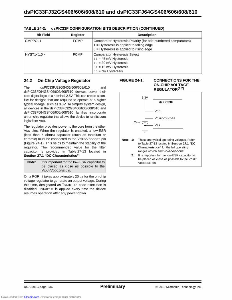
dsPIC33FJ32GS406/606/608/610 and dsPIC33FJ64GS406/606/608/610
DS70591C-page 336 Preliminary 2010 Microchip Technology Inc.
24.2 On-Chip Voltage Regulator
The dsPIC33FJ32GS406/606/608/610 anddsPIC33FJ64GS406/606/608/610 devices power theircore digital logic at a nominal 2.5V. This can create a con-flict for designs that are required to operate at a highertypical voltage, such as 3.3V. To simplify system design,all devices in the dsPIC33FJ32GS406/606/608/610 anddsPIC33FJ64GS406/606/608/610 families incorporatean on-chip regulator that allows the device to run its corelogic from VDD.
The regulator provides power to the core from the otherVDD pins. When the regulator is enabled, a low-ESR(less than 5 ohms) capacitor (such as tantalum orceramic) must be connected to the VCAP/VDDCORE pin(Figure 24-1). This helps to maintain the stability of theregulator. The recommended value for the filtercapacitor is provided in Table 27-13 located inSection 27.1 “DC Characteristics”.
On a POR, it takes approximately 20 s for the on-chipvoltage regulator to generate an output voltage. Duringthis time, designated as TSTARTUP, code execution isdisabled. TSTARTUP is applied every time the deviceresumes operation after any power-down.
FIGURE 24-1: CONNECTIONS FOR THE ON-CHIP VOLTAGE REGULATOR(1,2)
CMPPOL1 FCMP Comparator Hysteresis Polarity (for odd numbered comparators)1 = Hysteresis is applied to falling edge0 = Hysteresis is applied to rising edge
HYST1<1:0> FCMP Comparator Hysteresis Select11 = 45 mV Hysteresis10 = 30 mV Hysteresis01 = 15 mV Hysteresis00 = No Hysteresis
TABLE 24-2: dsPIC33F CONFIGURATION BITS DESCRIPTION (CONTINUED)
Bit Field Register Description
Note: It is important for the low-ESR capacitor tobe placed as close as possible to theVCAP/VDDCORE pin.
Note 1: These are typical operating voltages. Refer to Table 27-13 located in Section 27.1 “DC Characteristics” for the full operating ranges of VDD and VCAP/VDDCORE.
2: It is important for the low-ESR capacitor to be placed as close as possible to the VCAP/VDDCORE pin.
VDD
VCAP/VDDCORE
VSS
dsPIC33F
CEFC
3.3V
Downloaded from Elcodis.com electronic components distributor
2010 Microchip Technology Inc. Preliminary DS70591C-page 337
dsPIC33FJ32GS406/606/608/610 and dsPIC33FJ64GS406/606/608/610
24.3 BOR: Brown-Out Reset
The Brown-out Reset (BOR) module is based on aninternal voltage reference circuit that monitors theregulated supply voltage VCAP/VDDCORE. The mainpurpose of the BOR module is to generate a deviceReset when a brown-out condition occurs. Brown-outconditions are generally caused by glitches on the ACmains (for example, missing portions of the AC cyclewaveform due to bad power transmission lines, or volt-age sags due to excessive current draw when a largeinductive load is turned on).
A BOR generates a Reset pulse, which resets thedevice. The BOR selects the clock source, based onthe device Configuration bit values (FNOSC<2:0> andPOSCMD<1:0>).
If an oscillator mode is selected, the BOR activates theOscillator Start-up Timer (OST). The system clock isheld until OST expires. If the PLL is used, the clock isheld until the LOCK bit (OSCCON<5>) is ‘1’.
Concurrently, the PWRT time-out (TPWRT) is appliedbefore the internal Reset is released. If TPWRT = 0 anda crystal oscillator is being used, then a nominal delayof TFSCM = 100 is applied. The total delay in this caseis TFSCM.
The BOR Status bit (RCON<1>) is set to indicate that aBOR has occurred. The BOR circuit continues tooperate while in Sleep or Idle modes and resets thedevice should VDD fall below the BOR thresholdvoltage.
24.4 Watchdog Timer (WDT)
For dsPIC33FJ32GS406/606/608/610 anddsPIC33FJ64GS406/606/608/610 devices, the WDT isdriven by the LPRC oscillator. When the WDT is enabled,the clock source is also enabled.
24.4.1 PRESCALER/POSTSCALER
The nominal WDT clock source from LPRC is32.767 kHz. This feeds a prescaler that can be config-ured for either 5-bit (divide-by-32) or 7-bit (divide-by-128) operation. The prescaler is set by the WDTPREConfiguration bit. With a 32.767 kHz input, the pres-caler yields a nominal WDT time-out period (TWDT) of1 ms in 5-bit mode, or 4 ms in 7-bit mode.
A variable postscaler divides down the WDT prescaleroutput and allows for a wide range of time-out periods.The postscaler is controlled by the WDTPOST<3:0>Configuration bits (FWDT<3:0>) which allow theselection of 16 settings, from 1:1 to 1:32,768. Using theprescaler and postscaler, time-out periods ranging from1 ms to 131 seconds can be achieved.
The WDT, prescaler and postscaler are reset:
• On any device Reset
• On the completion of a clock switch, whether invoked by software (i.e., setting the OSWEN bit after changing the NOSC bits) or by hardware (i.e., Fail-Safe Clock Monitor)
• When a PWRSAV instruction is executed (i.e., Sleep or Idle mode is entered)
• When the device exits Sleep or Idle mode to resume normal operation
• By a CLRWDT instruction during normal execution
24.4.2 SLEEP AND IDLE MODES
If the WDT is enabled, it will continue to run duringSleep or Idle modes. When the WDT time-out occurs,the WDT will wake the device and code execution willcontinue from where the PWRSAV instruction wasexecuted. The corresponding SLEEP or IDLE bits(RCON<3:2>) will need to be cleared in software afterthe device wakes up.
24.4.3 ENABLING WDT
The WDT is enabled or disabled by the FWDTENConfiguration bit in the FWDT Configuration register.When the FWDTEN Configuration bit is set, the WDT isalways enabled.
The WDT can be optionally controlled in software whenthe FWDTEN Configuration bit has been programmedto ‘0’. The WDT is enabled in software by setting theSWDTEN control bit (RCON<5>). The SWDTENcontrol bit is cleared on any device Reset. The softwareWDT option allows the user application to enable theWDT for critical code segments and disable the WDTduring non-critical segments for maximum powersavings.
The WDT flag bit, WDTO (RCON<4>), is not automaticallycleared following a WDT time-out. To detect subsequentWDT events, the flag must be cleared in software.
Note: The CLRWDT and PWRSAV instructionsclear the prescaler and postscaler countswhen executed.
Note: If the WINDIS bit (FWDT<6>) is cleared, theCLRWDT instruction should be executed bythe application software only during the last1/4 of the WDT period. This CLRWDTwindow can be determined by using a timer.If a CLRWDT instruction is executed beforethis window, a WDT Reset occurs.
Downloaded from Elcodis.com electronic components distributor
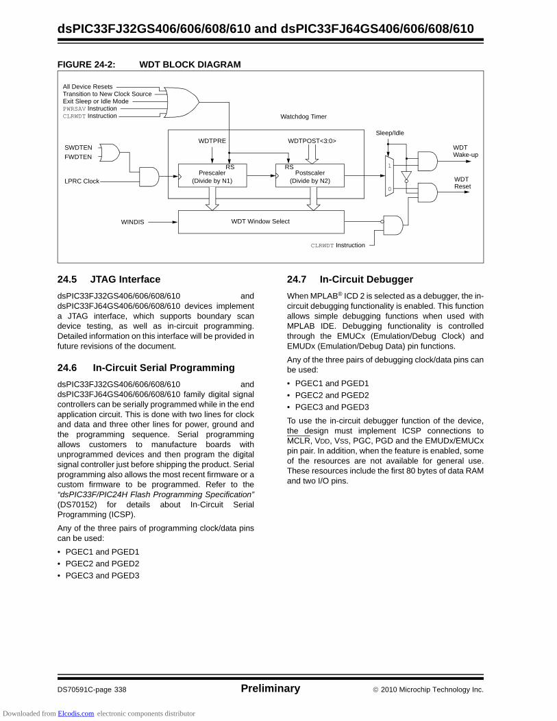
dsPIC33FJ32GS406/606/608/610 and dsPIC33FJ64GS406/606/608/610
DS70591C-page 338 Preliminary 2010 Microchip Technology Inc.
FIGURE 24-2: WDT BLOCK DIAGRAM
24.5 JTAG Interface
dsPIC33FJ32GS406/606/608/610 anddsPIC33FJ64GS406/606/608/610 devices implementa JTAG interface, which supports boundary scandevice testing, as well as in-circuit programming.Detailed information on this interface will be provided infuture revisions of the document.
24.6 In-Circuit Serial Programming
dsPIC33FJ32GS406/606/608/610 anddsPIC33FJ64GS406/606/608/610 family digital signalcontrollers can be serially programmed while in the endapplication circuit. This is done with two lines for clockand data and three other lines for power, ground andthe programming sequence. Serial programmingallows customers to manufacture boards withunprogrammed devices and then program the digitalsignal controller just before shipping the product. Serialprogramming also allows the most recent firmware or acustom firmware to be programmed. Refer to the“dsPIC33F/PIC24H Flash Programming Specification”(DS70152) for details about In-Circuit SerialProgramming (ICSP).
Any of the three pairs of programming clock/data pinscan be used:
• PGEC1 and PGED1
• PGEC2 and PGED2
• PGEC3 and PGED3
24.7 In-Circuit Debugger
When MPLAB® ICD 2 is selected as a debugger, the in-circuit debugging functionality is enabled. This functionallows simple debugging functions when used withMPLAB IDE. Debugging functionality is controlledthrough the EMUCx (Emulation/Debug Clock) andEMUDx (Emulation/Debug Data) pin functions.
Any of the three pairs of debugging clock/data pins canbe used:
• PGEC1 and PGED1
• PGEC2 and PGED2
• PGEC3 and PGED3
To use the in-circuit debugger function of the device,the design must implement ICSP connections toMCLR, VDD, VSS, PGC, PGD and the EMUDx/EMUCxpin pair. In addition, when the feature is enabled, someof the resources are not available for general use.These resources include the first 80 bytes of data RAMand two I/O pins.
All Device ResetsTransition to New Clock SourceExit Sleep or Idle ModePWRSAV InstructionCLRWDT Instruction
0
1
WDTPRE WDTPOST<3:0>
Watchdog Timer
Prescaler(Divide by N1)
Postscaler(Divide by N2)
Sleep/Idle
WDT
WDT Window SelectWINDIS
WDT
CLRWDT Instruction
SWDTEN
FWDTEN
LPRC Clock
RS RS
Wake-up
Reset
Downloaded from Elcodis.com electronic components distributor

2010 Microchip Technology Inc. Preliminary DS70591C-page 339
dsPIC33FJ32GS406/606/608/610 and dsPIC33FJ64GS406/606/608/610
24.8 Code Protection and CodeGuard™ Security
The dsPIC33FJ32GS406/606/608/610 anddsPIC33FJ64GS406/606/608/610 devices offer theintermediate implementation of CodeGuard™ Security.CodeGuard Security enables multiple parties to securelyshare resources (memory, interrupts and peripherals) ona single chip. This feature helps protect individualIntellectual Property in collaborative system designs.
When coupled with software encryption libraries,CodeGuard™ Security can be used to securely updateFlash even when multiple IPs reside on a single chip.
The code protection features are controlled by theConfiguration registers: FBS and FGS.
Secure segment and RAM protection is not implementedin dsPIC33FJ32GS406/606/608/610 anddsPIC33FJ64GS406/606/608/610 devices.
TABLE 24-3: CODE FLASH SECURITY SEGMENT SIZES FOR 64K BYTE DEVICES
TABLE 24-4: CODE FLASH SECURITY SEGMENT SIZES FOR 32K BYTE DEVICES
Note: Refer to the “CodeGuard SecurityReference Manual” (DS70180) for furtherinformation on usage, configuration andoperation of CodeGuard Security.
BSS<2:0> = x11 0K BSS<2:0> = x10 1K BSS<2:0> = x01 4K BSS<2:0> = x00 8K
BSS<2:0> = x11 0K BSS<2:0> = x10 1K BSS<2:0> = x01 4K BSS<2:0> = x00 8K
0001FEh000200h
000000hVS = 256 IW
00ABFEh
GS = 21760 IW
0001FEh000200h
000000hVS = 256 IW
0007FEh000800h
00ABFEh
GS = 20992 IW
BS = 768 IW0001FEh000200h
000000hVS = 256 IW
00ABFEh
001FFEh002000h
GS = 17920 IW
BS = 3840 IW
003FFEh004000h
0001FEh000200h
000000hVS = 256 IW
00ABFEh
GS = 13824 IW
BS = 7936 IW
0057FEh
0001FEh000200h
000000hVS = 256 IW
GS = 11008 IW
00ABFEh
0057FEh
0001FEh000200h
000000hVS = 256 IW
0007FEh000800h
GS = 10240 IW
BS = 768 IW
00ABFEh
0057FEh
0001FEh000200h
000000hVS = 256 IW
001FFEh002000h
GS = 7168 IW
BS = 3840 IW
00ABFEh
0057FEh
003FFEh004000h
0001FEh000200h
000000hVS = 256 IW
GS = 3072 IW
BS = 7936 IW
00ABFEh
Downloaded from Elcodis.com electronic components distributor

dsPIC33FJ32GS406/606/608/610 and dsPIC33FJ64GS406/606/608/610
DS70591C-page 340 Preliminary 2010 Microchip Technology Inc.
NOTES:
Downloaded from Elcodis.com electronic components distributor

2010 Microchip Technology Inc. Preliminary DS70591C-page 341
dsPIC33FJ32GS406/606/608/610 and dsPIC33FJ64GS406/606/608/610
25.0 INSTRUCTION SET SUMMARY
The dsPIC33F instruction set is identical to that of thedsPIC30F.
Most instructions are a single program memory word(24 bits). Only three instructions require two programmemory locations.
Each single-word instruction is a 24-bit word, dividedinto an 8-bit opcode, which specifies the instructiontype and one or more operands, which further specifythe operation of the instruction.
The instruction set is highly orthogonal and is groupedinto five basic categories:
• Word or byte-oriented operations
• Bit-oriented operations
• Literal operations
• DSP operations
• Control operations
Table 25-1 shows the general symbols used indescribing the instructions.
The dsPIC33F instruction set summary in Table 25-2lists all the instructions, along with the status flagsaffected by each instruction.
Most word or byte-oriented W register instructions(including barrel shift instructions) have threeoperands:
• The first source operand, which is typically a register ‘Wb’ without any address modifier
• The second source operand, which is typically a register ‘Ws’ with or without an address modifier
• The destination of the result, which is typically a register ‘Wd’ with or without an address modifier
However, word or byte-oriented file register instructionshave two operands:
• The file register specified by the value, ‘f’
• The destination, which could be either the file register, ‘f’, or the W0 register, which is denoted as ‘WREG’
Most bit-oriented instructions (including simplerotate/shift instructions) have two operands:
• The W register (with or without an address modifier) or file register (specified by the value of ‘Ws’ or ‘f’)
• The bit in the W register or file register (specified by a literal value or indirectly by the contents of register ‘Wb’)
The literal instructions that involve data movement canuse some of the following operands:
• A literal value to be loaded into a W register or file register (specified by ‘k’)
• The W register or file register where the literal value is to be loaded (specified by ‘Wb’ or ‘f’)
However, literal instructions that involve arithmetic orlogical operations use some of the following operands:
• The first source operand, which is a register ‘Wb’ without any address modifier
• The second source operand, which is a literal value
• The destination of the result (only if not the same as the first source operand), which is typically a register ‘Wd’ with or without an address modifier
The MAC class of DSP instructions can use some of thefollowing operands:
• The accumulator (A or B) to be used (required operand)
• The W registers to be used as the two operands
• The X and Y address space prefetch operations
• The X and Y address space prefetch destinations
• The accumulator write-back destination
The other DSP instructions do not involve anymultiplication and can include:
• The accumulator to be used (required)
• The source or destination operand (designated as Wso or Wdo, respectively) with or without an address modifier
• The amount of shift specified by a W register, ‘Wn’, or a literal value
The control instructions can use some of the followingoperands:
• A program memory address
• The mode of the table read and table write instructions
Note: This data sheet summarizes the featuresof the dsPIC33FJ32GS406/606/608/610and dsPIC33FJ64GS406/606/608/610devices. It is not intended to be acomprehensive reference source. Tocomplement the information in this datasheet, refer to the “dsPIC33F/PIC24HFamily Reference Manual”. Please seethe Microchip web site(www.microchip.com) for the latest“dsPIC33F/PIC24H Family ReferenceManual” sections.
Downloaded from Elcodis.com electronic components distributor

dsPIC33FJ32GS406/606/608/610 and dsPIC33FJ64GS406/606/608/610
DS70591C-page 342 Preliminary 2010 Microchip Technology Inc.
Most instructions are a single word. Certaindouble-word instructions are designed to provide all therequired information in these 48 bits. In the secondword, the 8 MSbs are ‘0’s. If this second word isexecuted as an instruction (by itself), it will execute asa NOP.
The double-word instructions execute in two instructioncycles.
Most single-word instructions are executed in a singleinstruction cycle, unless a conditional test is true, or theprogram counter is changed as a result of theinstruction. In these cases, the execution takes twoinstruction cycles with the additional instruction cycle(s)executed as a NOP. Notable exceptions are the BRA
(unconditional/computed branch), indirect CALL/GOTO,all table reads and writes and RETURN/RETFIEinstructions, which are single-word instructions but taketwo or three cycles. Certain instructions that involveskipping over the subsequent instruction require eithertwo or three cycles if the skip is performed, dependingon whether the instruction being skipped is a single-wordor two-word instruction. Moreover, double-word movesrequire two cycles.
Note: For more details on the instruction set,refer to the “16-bit MCU and DSCProgrammer’s Reference Manual”(DS70157).
TABLE 25-1: SYMBOLS USED IN OPCODE DESCRIPTIONS
Field Description
#text Means literal defined by “text”
(text) Means “content of text”
[text] Means “the location addressed by text”
{ } Optional field or operation
<n:m> Register bit field
.b Byte mode selection
.d Double-Word mode selection
.S Shadow register select
.w Word mode selection (default)
Acc One of two accumulators {A, B}
AWB Accumulator Write-Back Destination Address register {W13, [W13]+ = 2}
bit4 4-bit bit selection field (used in word-addressed instructions) {0...15}
C, DC, N, OV, Z MCU Status bits: Carry, Digit Carry, Negative, Overflow, Sticky Zero
Expr Absolute address, label or expression (resolved by the linker)
f File register address {0x0000...0x1FFF}
lit1 1-bit unsigned literal {0,1}
lit4 4-bit unsigned literal {0...15}
lit5 5-bit unsigned literal {0...31}
lit8 8-bit unsigned literal {0...255}
lit10 10-bit unsigned literal {0...255} for Byte mode, {0:1023} for Word mode
lit14 14-bit unsigned literal {0...16384}
lit16 16-bit unsigned literal {0...65535}
lit23 23-bit unsigned literal {0...8388608}; LSb must be ‘0’
None Field does not require an entry, can be blank
OA, OB, SA, SB DSP Status bits: ACCA Overflow, ACCB Overflow, ACCA Saturate, ACCB Saturate
PC Program Counter
Slit10 10-bit signed literal {-512...511}
Slit16 16-bit signed literal {-32768...32767}
Slit6 6-bit signed literal {-16...16}
Wb Base W register {W0..W15}
Wd Destination W register { Wd, [Wd], [Wd++], [Wd--], [++Wd], [--Wd] }
Wdo Destination W register { Wnd, [Wnd], [Wnd++], [Wnd--], [++Wnd], [--Wnd], [Wnd+Wb] }
Wm,Wn Dividend, Divisor Working register pair (Direct Addressing)
Downloaded from Elcodis.com electronic components distributor

2010 Microchip Technology Inc. Preliminary DS70591C-page 343
dsPIC33FJ32GS406/606/608/610 and dsPIC33FJ64GS406/606/608/610
Wm*Wm Multiplicand and Multiplier Working register pair for Square instructions {W4 * W4,W5 * W5,W6 * W6,W7 * W7}
Wm*Wn Multiplicand and Multiplier Working register pair for DSP instructions {W4 * W5,W4 * W6,W4 * W7,W5 * W6,W5 * W7,W6 * W7}
Wn One of 16 Working registers {W0..W15}
Wnd One of 16 Destination Working registers {W0...W15}
Wns One of 16 Source Working registers {W0...W15}
WREG W0 (Working register used in file register instructions)
Ws Source W register { Ws, [Ws], [Ws++], [Ws--], [++Ws], [--Ws] }
Wso Source W register { Wns, [Wns], [Wns++], [Wns--], [++Wns], [--Wns], [Wns+Wb] }
Wx X Data Space Prefetch Address register for DSP instructions {[W8] + = 6, [W8] + = 4, [W8] + = 2, [W8], [W8] - = 6, [W8] - = 4, [W8] - = 2, [W9] + = 6, [W9] + = 4, [W9] + = 2, [W9], [W9] - = 6, [W9] - = 4, [W9] - = 2, [W9 + W12], none}
Wxd X Data Space Prefetch Destination register for DSP instructions {W4...W7}
Wy Y Data Space Prefetch Address register for DSP instructions {[W10] + = 6, [W10] + = 4, [W10] + = 2, [W10], [W10] - = 6, [W10] - = 4, [W10] - = 2, [W11] + = 6, [W11] + = 4, [W11] + = 2, [W11], [W11] - = 6, [W11] - = 4, [W11] - = 2, [W11 + W12], none}
Wyd Y Data Space Prefetch Destination register for DSP instructions {W4...W7}
TABLE 25-1: SYMBOLS USED IN OPCODE DESCRIPTIONS (CONTINUED)
Field Description
Downloaded from Elcodis.com electronic components distributor
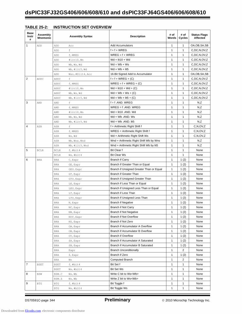
dsPIC33FJ32GS406/606/608/610 and dsPIC33FJ64GS406/606/608/610
DS70591C-page 344 Preliminary 2010 Microchip Technology Inc.
TABLE 25-2: INSTRUCTION SET OVERVIEW
BaseInstr
#
AssemblyMnemonic
Assembly Syntax Description# of
Words# of
CyclesStatus Flags
Affected
1 ADD ADD Acc Add Accumulators 1 1 OA,OB,SA,SB
ADD f f = f + WREG 1 1 C,DC,N,OV,Z
ADD f,WREG WREG = f + WREG 1 1 C,DC,N,OV,Z
ADD #lit10,Wn Wd = lit10 + Wd 1 1 C,DC,N,OV,Z
ADD Wb,Ws,Wd Wd = Wb + Ws 1 1 C,DC,N,OV,Z
ADD Wb,#lit5,Wd Wd = Wb + lit5 1 1 C,DC,N,OV,Z
ADD Wso,#Slit4,Acc 16-Bit Signed Add to Accumulator 1 1 OA,OB,SA,SB
2 ADDC ADDC f f = f + WREG + (C) 1 1 C,DC,N,OV,Z
ADDC f,WREG WREG = f + WREG + (C) 1 1 C,DC,N,OV,Z
ADDC #lit10,Wn Wd = lit10 + Wd + (C) 1 1 C,DC,N,OV,Z
ADDC Wb,Ws,Wd Wd = Wb + Ws + (C) 1 1 C,DC,N,OV,Z
ADDC Wb,#lit5,Wd Wd = Wb + lit5 + (C) 1 1 C,DC,N,OV,Z
3 AND AND f f = f .AND. WREG 1 1 N,Z
AND f,WREG WREG = f .AND. WREG 1 1 N,Z
AND #lit10,Wn Wd = lit10 .AND. Wd 1 1 N,Z
AND Wb,Ws,Wd Wd = Wb .AND. Ws 1 1 N,Z
AND Wb,#lit5,Wd Wd = Wb .AND. lit5 1 1 N,Z
4 ASR ASR f f = Arithmetic Right Shift f 1 1 C,N,OV,Z
ASR f,WREG WREG = Arithmetic Right Shift f 1 1 C,N,OV,Z
ASR Ws,Wd Wd = Arithmetic Right Shift Ws 1 1 C,N,OV,Z
ASR Wb,Wns,Wnd Wnd = Arithmetic Right Shift Wb by Wns 1 1 N,Z
ASR Wb,#lit5,Wnd Wnd = Arithmetic Right Shift Wb by lit5 1 1 N,Z
5 BCLR BCLR f,#bit4 Bit Clear f 1 1 None
BCLR Ws,#bit4 Bit Clear Ws 1 1 None
6 BRA BRA C,Expr Branch if Carry 1 1 (2) None
BRA GE,Expr Branch if Greater Than or Equal 1 1 (2) None
BRA GEU,Expr Branch if Unsigned Greater Than or Equal 1 1 (2) None
BRA GT,Expr Branch if Greater Than 1 1 (2) None
BRA GTU,Expr Branch if Unsigned Greater Than 1 1 (2) None
BRA LE,Expr Branch if Less Than or Equal 1 1 (2) None
BRA LEU,Expr Branch if Unsigned Less Than or Equal 1 1 (2) None
BRA LT,Expr Branch if Less Than 1 1 (2) None
BRA LTU,Expr Branch if Unsigned Less Than 1 1 (2) None
BRA N,Expr Branch if Negative 1 1 (2) None
BRA NC,Expr Branch if Not Carry 1 1 (2) None
BRA NN,Expr Branch if Not Negative 1 1 (2) None
BRA NOV,Expr Branch if Not Overflow 1 1 (2) None
BRA NZ,Expr Branch if Not Zero 1 1 (2) None
BRA OA,Expr Branch if Accumulator A Overflow 1 1 (2) None
BRA OB,Expr Branch if Accumulator B Overflow 1 1 (2) None
BRA OV,Expr Branch if Overflow 1 1 (2) None
BRA SA,Expr Branch if Accumulator A Saturated 1 1 (2) None
BRA SB,Expr Branch if Accumulator B Saturated 1 1 (2) None
BRA Expr Branch Unconditionally 1 2 None
BRA Z,Expr Branch if Zero 1 1 (2) None
BRA Wn Computed Branch 1 2 None
7 BSET BSET f,#bit4 Bit Set f 1 1 None
BSET Ws,#bit4 Bit Set Ws 1 1 None
8 BSW BSW.C Ws,Wb Write C bit to Ws<Wb> 1 1 None
BSW.Z Ws,Wb Write Z bit to Ws<Wb> 1 1 None
9 BTG BTG f,#bit4 Bit Toggle f 1 1 None
BTG Ws,#bit4 Bit Toggle Ws 1 1 None
Downloaded from Elcodis.com electronic components distributor
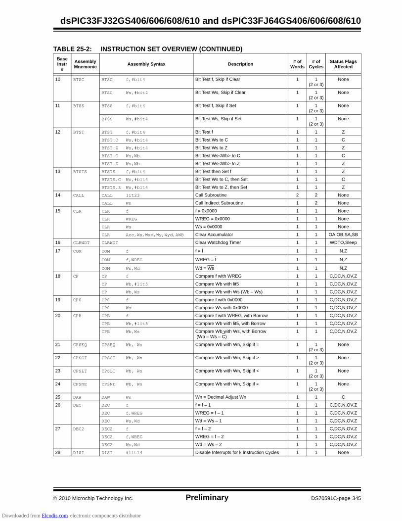
2010 Microchip Technology Inc. Preliminary DS70591C-page 345
dsPIC33FJ32GS406/606/608/610 and dsPIC33FJ64GS406/606/608/610
10 BTSC BTSC f,#bit4 Bit Test f, Skip if Clear 1 1 (2 or 3)
None
BTSC Ws,#bit4 Bit Test Ws, Skip if Clear 1 1 (2 or 3)
None
11 BTSS BTSS f,#bit4 Bit Test f, Skip if Set 1 1 (2 or 3)
None
BTSS Ws,#bit4 Bit Test Ws, Skip if Set 1 1 (2 or 3)
None
12 BTST BTST f,#bit4 Bit Test f 1 1 Z
BTST.C Ws,#bit4 Bit Test Ws to C 1 1 C
BTST.Z Ws,#bit4 Bit Test Ws to Z 1 1 Z
BTST.C Ws,Wb Bit Test Ws<Wb> to C 1 1 C
BTST.Z Ws,Wb Bit Test Ws<Wb> to Z 1 1 Z
13 BTSTS BTSTS f,#bit4 Bit Test then Set f 1 1 Z
BTSTS.C Ws,#bit4 Bit Test Ws to C, then Set 1 1 C
BTSTS.Z Ws,#bit4 Bit Test Ws to Z, then Set 1 1 Z
14 CALL CALL lit23 Call Subroutine 2 2 None
CALL Wn Call Indirect Subroutine 1 2 None
15 CLR CLR f f = 0x0000 1 1 None
CLR WREG WREG = 0x0000 1 1 None
CLR Ws Ws = 0x0000 1 1 None
CLR Acc,Wx,Wxd,Wy,Wyd,AWB Clear Accumulator 1 1 OA,OB,SA,SB
16 CLRWDT CLRWDT Clear Watchdog Timer 1 1 WDTO,Sleep
17 COM COM f f = f 1 1 N,Z
COM f,WREG WREG = f 1 1 N,Z
COM Ws,Wd Wd = Ws 1 1 N,Z
18 CP CP f Compare f with WREG 1 1 C,DC,N,OV,Z
CP Wb,#lit5 Compare Wb with lit5 1 1 C,DC,N,OV,Z
CP Wb,Ws Compare Wb with Ws (Wb – Ws) 1 1 C,DC,N,OV,Z
19 CP0 CP0 f Compare f with 0x0000 1 1 C,DC,N,OV,Z
CP0 Ws Compare Ws with 0x0000 1 1 C,DC,N,OV,Z
20 CPB CPB f Compare f with WREG, with Borrow 1 1 C,DC,N,OV,Z
CPB Wb,#lit5 Compare Wb with lit5, with Borrow 1 1 C,DC,N,OV,Z
CPB Wb,Ws Compare Wb with Ws, with Borrow (Wb – Ws – C)
1 1 C,DC,N,OV,Z
21 CPSEQ CPSEQ Wb, Wn Compare Wb with Wn, Skip if = 1 1 (2 or 3)
None
22 CPSGT CPSGT Wb, Wn Compare Wb with Wn, Skip if > 1 1 (2 or 3)
None
23 CPSLT CPSLT Wb, Wn Compare Wb with Wn, Skip if < 1 1 (2 or 3)
None
24 CPSNE CPSNE Wb, Wn Compare Wb with Wn, Skip if 1 1 (2 or 3)
None
25 DAW DAW Wn Wn = Decimal Adjust Wn 1 1 C
26 DEC DEC f f = f – 1 1 1 C,DC,N,OV,Z
DEC f,WREG WREG = f – 1 1 1 C,DC,N,OV,Z
DEC Ws,Wd Wd = Ws – 1 1 1 C,DC,N,OV,Z
27 DEC2 DEC2 f f = f – 2 1 1 C,DC,N,OV,Z
DEC2 f,WREG WREG = f – 2 1 1 C,DC,N,OV,Z
DEC2 Ws,Wd Wd = Ws – 2 1 1 C,DC,N,OV,Z
28 DISI DISI #lit14 Disable Interrupts for k Instruction Cycles 1 1 None
TABLE 25-2: INSTRUCTION SET OVERVIEW (CONTINUED)
BaseInstr
#
AssemblyMnemonic
Assembly Syntax Description# of
Words# of
CyclesStatus Flags
Affected
Downloaded from Elcodis.com electronic components distributor
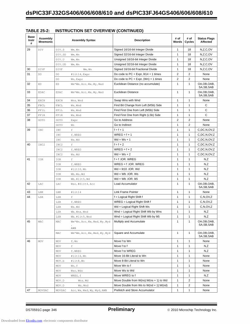
dsPIC33FJ32GS406/606/608/610 and dsPIC33FJ64GS406/606/608/610
DS70591C-page 346 Preliminary 2010 Microchip Technology Inc.
29 DIV DIV.S Wm,Wn Signed 16/16-bit Integer Divide 1 18 N,Z,C,OV
DIV.SD Wm,Wn Signed 32/16-bit Integer Divide 1 18 N,Z,C,OV
DIV.U Wm,Wn Unsigned 16/16-bit Integer Divide 1 18 N,Z,C,OV
DIV.UD Wm,Wn Unsigned 32/16-bit Integer Divide 1 18 N,Z,C,OV
30 DIVF DIVF Wm,Wn Signed 16/16-bit Fractional Divide 1 18 N,Z,C,OV
31 DO DO #lit14,Expr Do code to PC + Expr, lit14 + 1 times 2 2 None
DO Wn,Expr Do code to PC + Expr, (Wn) + 1 times 2 2 None
32 ED ED Wm*Wm,Acc,Wx,Wy,Wxd Euclidean Distance (no accumulate) 1 1 OA,OB,OAB,SA,SB,SAB
33 EDAC EDAC Wm*Wm,Acc,Wx,Wy,Wxd Euclidean Distance 1 1 OA,OB,OAB,SA,SB,SAB
34 EXCH EXCH Wns,Wnd Swap Wns with Wnd 1 1 None
35 FBCL FBCL Ws,Wnd Find Bit Change from Left (MSb) Side 1 1 C
36 FF1L FF1L Ws,Wnd Find First One from Left (MSb) Side 1 1 C
37 FF1R FF1R Ws,Wnd Find First One from Right (LSb) Side 1 1 C
38 GOTO GOTO Expr Go to Address 2 2 None
GOTO Wn Go to Indirect 1 2 None
39 INC INC f f = f + 1 1 1 C,DC,N,OV,Z
INC f,WREG WREG = f + 1 1 1 C,DC,N,OV,Z
INC Ws,Wd Wd = Ws + 1 1 1 C,DC,N,OV,Z
40 INC2 INC2 f f = f + 2 1 1 C,DC,N,OV,Z
INC2 f,WREG WREG = f + 2 1 1 C,DC,N,OV,Z
INC2 Ws,Wd Wd = Ws + 2 1 1 C,DC,N,OV,Z
41 IOR IOR f f = f .IOR. WREG 1 1 N,Z
IOR f,WREG WREG = f .IOR. WREG 1 1 N,Z
IOR #lit10,Wn Wd = lit10 .IOR. Wd 1 1 N,Z
IOR Wb,Ws,Wd Wd = Wb .IOR. Ws 1 1 N,Z
IOR Wb,#lit5,Wd Wd = Wb .IOR. lit5 1 1 N,Z
42 LAC LAC Wso,#Slit4,Acc Load Accumulator 1 1 OA,OB,OAB,SA,SB,SAB
43 LNK LNK #lit14 Link Frame Pointer 1 1 None
44 LSR LSR f f = Logical Right Shift f 1 1 C,N,OV,Z
LSR f,WREG WREG = Logical Right Shift f 1 1 C,N,OV,Z
LSR Ws,Wd Wd = Logical Right Shift Ws 1 1 C,N,OV,Z
LSR Wb,Wns,Wnd Wnd = Logical Right Shift Wb by Wns 1 1 N,Z
LSR Wb,#lit5,Wnd Wnd = Logical Right Shift Wb by lit5 1 1 N,Z
45 MAC MAC Wm*Wn,Acc,Wx,Wxd,Wy,Wyd,AWB
Multiply and Accumulate 1 1 OA,OB,OAB,SA,SB,SAB
MAC Wm*Wm,Acc,Wx,Wxd,Wy,Wyd Square and Accumulate 1 1 OA,OB,OAB,SA,SB,SAB
46 MOV MOV f,Wn Move f to Wn 1 1 None
MOV f Move f to f 1 1 N,Z
MOV f,WREG Move f to WREG 1 1 N,Z
MOV #lit16,Wn Move 16-Bit Literal to Wn 1 1 None
MOV.b #lit8,Wn Move 8-Bit Literal to Wn 1 1 None
MOV Wn,f Move Wn to f 1 1 None
MOV Wso,Wdo Move Ws to Wd 1 1 None
MOV WREG,f Move WREG to f 1 1 N,Z
MOV.D Wns,Wd Move Double from W(ns):W(ns + 1) to Wd 1 2 None
MOV.D Ws,Wnd Move Double from Ws to W(nd + 1):W(nd) 1 2 None
47 MOVSAC MOVSAC Acc,Wx,Wxd,Wy,Wyd,AWB Prefetch and Store Accumulator 1 1 None
TABLE 25-2: INSTRUCTION SET OVERVIEW (CONTINUED)
BaseInstr
#
AssemblyMnemonic
Assembly Syntax Description# of
Words# of
CyclesStatus Flags
Affected
Downloaded from Elcodis.com electronic components distributor

2010 Microchip Technology Inc. Preliminary DS70591C-page 347
dsPIC33FJ32GS406/606/608/610 and dsPIC33FJ64GS406/606/608/610
48 MPY MPY Wm*Wn,Acc,Wx,Wxd,Wy,Wyd
Multiply Wm by Wn to Accumulator 1 1 OA,OB,OAB,SA,SB,SAB
MPY Wm*Wm,Acc,Wx,Wxd,Wy,Wyd
Square Wm to Accumulator 1 1 OA,OB,OAB,SA,SB,SAB
49 MPY.N MPY.N Wm*Wn,Acc,Wx,Wxd,Wy,Wyd
-(Multiply Wm by Wn) to Accumulator 1 1 None
50 MSC MSC Wm*Wm,Acc,Wx,Wxd,Wy,Wyd,AWB
Multiply and Subtract from Accumulator 1 1 OA,OB,OAB,SA,SB,SAB
51 MUL MUL.SS Wb,Ws,Wnd {Wnd + 1, Wnd} = signed(Wb) * signed(Ws) 1 1 None
MUL.SU Wb,Ws,Wnd {Wnd + 1, Wnd} = signed(Wb) * unsigned(Ws) 1 1 None
MUL.US Wb,Ws,Wnd {Wnd + 1, Wnd} = unsigned(Wb) * signed(Ws) 1 1 None
MUL.UU Wb,Ws,Wnd {Wnd + 1, Wnd} = unsigned(Wb) * unsigned(Ws)
1 1 None
MUL.SU Wb,#lit5,Wnd {Wnd + 1, Wnd} = signed(Wb) * unsigned(lit5) 1 1 None
MUL.UU Wb,#lit5,Wnd {Wnd + 1, Wnd} = unsigned(Wb) * unsigned(lit5)
1 1 None
MUL f W3:W2 = f * WREG 1 1 None
52 NEG NEG Acc Negate Accumulator 1 1 OA,OB,OAB,SA,SB,SAB
NEG f f = f + 1 1 1 C,DC,N,OV,Z
NEG f,WREG WREG = f + 1 1 1 C,DC,N,OV,Z
NEG Ws,Wd Wd = Ws + 1 1 1 C,DC,N,OV,Z
53 NOP NOP No Operation 1 1 None
NOPR No Operation 1 1 None
54 POP POP f Pop f from Top-of-Stack (TOS) 1 1 None
POP Wdo Pop from Top-of-Stack (TOS) to Wdo 1 1 None
POP.D Wnd Pop from Top-of-Stack (TOS) to W(nd):W(nd + 1)
1 2 None
POP.S Pop Shadow Registers 1 1 All
55 PUSH PUSH f Push f to Top-of-Stack (TOS) 1 1 None
PUSH Wso Push Wso to Top-of-Stack (TOS) 1 1 None
PUSH.D Wns Push W(ns):W(ns + 1) to Top-of-Stack (TOS) 1 2 None
PUSH.S Push Shadow Registers 1 1 None
56 PWRSAV PWRSAV #lit1 Go into Sleep or Idle mode 1 1 WDTO,Sleep
57 RCALL RCALL Expr Relative Call 1 2 None
RCALL Wn Computed Call 1 2 None
58 REPEAT REPEAT #lit14 Repeat Next Instruction lit14 + 1 times 1 1 None
REPEAT Wn Repeat Next Instruction (Wn) + 1 times 1 1 None
59 RESET RESET Software Device Reset 1 1 None
60 RETFIE RETFIE Return from interrupt 1 3 (2) None
61 RETLW RETLW #lit10,Wn Return with Literal in Wn 1 3 (2) None
62 RETURN RETURN Return from Subroutine 1 3 (2) None
63 RLC RLC f f = Rotate Left through Carry f 1 1 C,N,Z
RLC f,WREG WREG = Rotate Left through Carry f 1 1 C,N,Z
RLC Ws,Wd Wd = Rotate Left through Carry Ws 1 1 C,N,Z
64 RLNC RLNC f f = Rotate Left (No Carry) f 1 1 N,Z
RLNC f,WREG WREG = Rotate Left (No Carry) f 1 1 N,Z
RLNC Ws,Wd Wd = Rotate Left (No Carry) Ws 1 1 N,Z
65 RRC RRC f f = Rotate Right through Carry f 1 1 C,N,Z
RRC f,WREG WREG = Rotate Right through Carry f 1 1 C,N,Z
RRC Ws,Wd Wd = Rotate Right through Carry Ws 1 1 C,N,Z
TABLE 25-2: INSTRUCTION SET OVERVIEW (CONTINUED)
BaseInstr
#
AssemblyMnemonic
Assembly Syntax Description# of
Words# of
CyclesStatus Flags
Affected
Downloaded from Elcodis.com electronic components distributor

dsPIC33FJ32GS406/606/608/610 and dsPIC33FJ64GS406/606/608/610
DS70591C-page 348 Preliminary 2010 Microchip Technology Inc.
66 RRNC RRNC f f = Rotate Right (No Carry) f 1 1 N,Z
RRNC f,WREG WREG = Rotate Right (No Carry) f 1 1 N,Z
RRNC Ws,Wd Wd = Rotate Right (No Carry) Ws 1 1 N,Z
67 SAC SAC Acc,#Slit4,Wdo Store Accumulator 1 1 None
SAC.R Acc,#Slit4,Wdo Store Rounded Accumulator 1 1 None
68 SE SE Ws,Wnd Wnd = Sign-Extended Ws 1 1 C,N,Z
69 SETM SETM f f = 0xFFFF 1 1 None
SETM WREG WREG = 0xFFFF 1 1 None
SETM Ws Ws = 0xFFFF 1 1 None
70 SFTAC SFTAC Acc,Wn Arithmetic Shift Accumulator by (Wn) 1 1 OA,OB,OAB,SA,SB,SAB
SFTAC Acc,#Slit6 Arithmetic Shift Accumulator by Slit6 1 1 OA,OB,OAB,SA,SB,SAB
71 SL SL f f = Left Shift f 1 1 C,N,OV,Z
SL f,WREG WREG = Left Shift f 1 1 C,N,OV,Z
SL Ws,Wd Wd = Left Shift Ws 1 1 C,N,OV,Z
SL Wb,Wns,Wnd Wnd = Left Shift Wb by Wns 1 1 N,Z
SL Wb,#lit5,Wnd Wnd = Left Shift Wb by lit5 1 1 N,Z
72 SUB SUB Acc Subtract Accumulators 1 1 OA,OB,OAB,SA,SB,SAB
SUB f f = f – WREG 1 1 C,DC,N,OV,Z
SUB f,WREG WREG = f – WREG 1 1 C,DC,N,OV,Z
SUB #lit10,Wn Wn = Wn – lit10 1 1 C,DC,N,OV,Z
SUB Wb,Ws,Wd Wd = Wb – Ws 1 1 C,DC,N,OV,Z
SUB Wb,#lit5,Wd Wd = Wb – lit5 1 1 C,DC,N,OV,Z
73 SUBB SUBB f f = f – WREG – (C) 1 1 C,DC,N,OV,Z
SUBB f,WREG WREG = f – WREG – (C) 1 1 C,DC,N,OV,Z
SUBB #lit10,Wn Wn = Wn – lit10 – (C) 1 1 C,DC,N,OV,Z
SUBB Wb,Ws,Wd Wd = Wb – Ws – (C) 1 1 C,DC,N,OV,Z
SUBB Wb,#lit5,Wd Wd = Wb – lit5 – (C) 1 1 C,DC,N,OV,Z
74 SUBR SUBR f f = WREG – f 1 1 C,DC,N,OV,Z
SUBR f,WREG WREG = WREG – f 1 1 C,DC,N,OV,Z
SUBR Wb,Ws,Wd Wd = Ws – Wb 1 1 C,DC,N,OV,Z
SUBR Wb,#lit5,Wd Wd = lit5 – Wb 1 1 C,DC,N,OV,Z
75 SUBBR SUBBR f f = WREG – f – (C) 1 1 C,DC,N,OV,Z
SUBBR f,WREG WREG = WREG – f – (C) 1 1 C,DC,N,OV,Z
SUBBR Wb,Ws,Wd Wd = Ws – Wb – (C) 1 1 C,DC,N,OV,Z
SUBBR Wb,#lit5,Wd Wd = lit5 – Wb – (C) 1 1 C,DC,N,OV,Z
76 SWAP SWAP.b Wn Wn = Nibble Swap Wn 1 1 None
SWAP Wn Wn = Byte Swap Wn 1 1 None
77 TBLRDH TBLRDH Ws,Wd Read Prog<23:16> to Wd<7:0> 1 2 None
78 TBLRDL TBLRDL Ws,Wd Read Prog<15:0> to Wd 1 2 None
79 TBLWTH TBLWTH Ws,Wd Write Ws<7:0> to Prog<23:16> 1 2 None
80 TBLWTL TBLWTL Ws,Wd Write Ws to Prog<15:0> 1 2 None
81 ULNK ULNK Unlink Frame Pointer 1 1 None
82 XOR XOR f f = f .XOR. WREG 1 1 N,Z
XOR f,WREG WREG = f .XOR. WREG 1 1 N,Z
XOR #lit10,Wn Wd = lit10 .XOR. Wd 1 1 N,Z
XOR Wb,Ws,Wd Wd = Wb .XOR. Ws 1 1 N,Z
XOR Wb,#lit5,Wd Wd = Wb .XOR. lit5 1 1 N,Z
83 ZE ZE Ws,Wnd Wnd = Zero-Extend Ws 1 1 C,Z,N
TABLE 25-2: INSTRUCTION SET OVERVIEW (CONTINUED)
BaseInstr
#
AssemblyMnemonic
Assembly Syntax Description# of
Words# of
CyclesStatus Flags
Affected
Downloaded from Elcodis.com electronic components distributor

2010 Microchip Technology Inc. Preliminary DS70591C-page 349
dsPIC33FJ32GS406/606/608/610 and dsPIC33FJ64GS406/606/608/610
26.0 DEVELOPMENT SUPPORT
The PIC® microcontrollers and dsPIC® digital signalcontrollers are supported with a full range of softwareand hardware development tools:
• Integrated Development Environment
- MPLAB® IDE Software
• Compilers/Assemblers/Linkers
- MPLAB C Compiler for Various DeviceFamilies
- HI-TECH C for Various Device Families
- MPASMTM Assembler
- MPLINKTM Object Linker/MPLIBTM Object Librarian
- MPLAB Assembler/Linker/Librarian forVarious Device Families
• Simulators
- MPLAB SIM Software Simulator
• Emulators
- MPLAB REAL ICE™ In-Circuit Emulator
• In-Circuit Debuggers
- MPLAB ICD 3
- PICkit™ 3 Debug Express
• Device Programmers
- PICkit™ 2 Programmer
- MPLAB PM3 Device Programmer
• Low-Cost Demonstration/Development Boards, Evaluation Kits, and Starter Kits
26.1 MPLAB Integrated Development Environment Software
The MPLAB IDE software brings an ease of softwaredevelopment previously unseen in the 8/16/32-bitmicrocontroller market. The MPLAB IDE is a Windows®
operating system-based application that contains:
• A single graphical interface to all debugging tools
- Simulator
- Programmer (sold separately)
- In-Circuit Emulator (sold separately)
- In-Circuit Debugger (sold separately)
• A full-featured editor with color-coded context
• A multiple project manager
• Customizable data windows with direct edit of contents
• High-level source code debugging
• Mouse over variable inspection
• Drag and drop variables from source to watch windows
• Extensive on-line help
• Integration of select third-party tools, such as IAR C Compilers
The MPLAB IDE allows you to:
• Edit your source files (either C or assembly)
• One-touch compile or assemble, and download to emulator and simulator tools (automatically updates all project information)
• Debug using:
- Source files (C or assembly)
- Mixed C and assembly
- Machine code
MPLAB IDE supports multiple debugging tools in asingle development paradigm, from the cost-effectivesimulators, through low-cost in-circuit debuggers, tofull-featured emulators. This eliminates the learningcurve when upgrading to tools with increased flexibilityand power.
Downloaded from Elcodis.com electronic components distributor

dsPIC33FJ32GS406/606/608/610 and dsPIC33FJ64GS406/606/608/610
DS70591C-page 350 Preliminary 2010 Microchip Technology Inc.
26.2 MPLAB C Compilers for Various Device Families
The MPLAB C Compiler code development systemsare complete ANSI C compilers for Microchip’s PIC18,PIC24 and PIC32 families of microcontrollers and thedsPIC30 and dsPIC33 families of digital signal control-lers. These compilers provide powerful integrationcapabilities, superior code optimization and ease ofuse.
For easy source level debugging, the compilers providesymbol information that is optimized to the MPLAB IDEdebugger.
26.3 HI-TECH C for Various Device Families
The HI-TECH C Compiler code development systemsare complete ANSI C compilers for Microchip’s PICfamily of microcontrollers and the dsPIC family of digitalsignal controllers. These compilers provide powerfulintegration capabilities, omniscient code generationand ease of use.
For easy source level debugging, the compilers providesymbol information that is optimized to the MPLAB IDEdebugger.
The compilers include a macro assembler, linker, pre-processor, and one-step driver, and can run on multipleplatforms.
26.4 MPASM Assembler
The MPASM Assembler is a full-featured, universalmacro assembler for PIC10/12/16/18 MCUs.
The MPASM Assembler generates relocatable objectfiles for the MPLINK Object Linker, Intel® standard HEXfiles, MAP files to detail memory usage and symbolreference, absolute LST files that contain source linesand generated machine code and COFF files fordebugging.
The MPASM Assembler features include:
• Integration into MPLAB IDE projects
• User-defined macros to streamline assembly code
• Conditional assembly for multi-purpose source files
• Directives that allow complete control over the assembly process
26.5 MPLINK Object Linker/MPLIB Object Librarian
The MPLINK Object Linker combines relocatableobjects created by the MPASM Assembler and theMPLAB C18 C Compiler. It can link relocatable objectsfrom precompiled libraries, using directives from alinker script.
The MPLIB Object Librarian manages the creation andmodification of library files of precompiled code. Whena routine from a library is called from a source file, onlythe modules that contain that routine will be linked inwith the application. This allows large libraries to beused efficiently in many different applications.
The object linker/library features include:
• Efficient linking of single libraries instead of many smaller files
• Enhanced code maintainability by grouping related modules together
• Flexible creation of libraries with easy module listing, replacement, deletion and extraction
26.6 MPLAB Assembler, Linker and Librarian for Various Device Families
MPLAB Assembler produces relocatable machinecode from symbolic assembly language for PIC24,PIC32 and dsPIC devices. MPLAB C Compiler usesthe assembler to produce its object file. The assemblergenerates relocatable object files that can then bearchived or linked with other relocatable object files andarchives to create an executable file. Notable featuresof the assembler include:
• Support for the entire device instruction set
• Support for fixed-point and floating-point data
• Command line interface
• Rich directive set
• Flexible macro language
• MPLAB IDE compatibility
Downloaded from Elcodis.com electronic components distributor
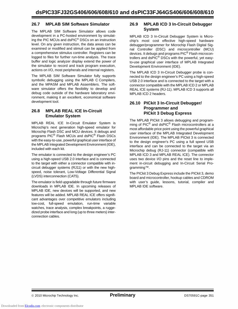
2010 Microchip Technology Inc. Preliminary DS70591C-page 351
dsPIC33FJ32GS406/606/608/610 and dsPIC33FJ64GS406/606/608/610
26.7 MPLAB SIM Software Simulator
The MPLAB SIM Software Simulator allows codedevelopment in a PC-hosted environment by simulat-ing the PIC MCUs and dsPIC® DSCs on an instructionlevel. On any given instruction, the data areas can beexamined or modified and stimuli can be applied froma comprehensive stimulus controller. Registers can belogged to files for further run-time analysis. The tracebuffer and logic analyzer display extend the power ofthe simulator to record and track program execution,actions on I/O, most peripherals and internal registers.
The MPLAB SIM Software Simulator fully supportssymbolic debugging using the MPLAB C Compilers,and the MPASM and MPLAB Assemblers. The soft-ware simulator offers the flexibility to develop anddebug code outside of the hardware laboratory envi-ronment, making it an excellent, economical softwaredevelopment tool.
26.8 MPLAB REAL ICE In-Circuit Emulator System
MPLAB REAL ICE In-Circuit Emulator System isMicrochip’s next generation high-speed emulator forMicrochip Flash DSC and MCU devices. It debugs andprograms PIC® Flash MCUs and dsPIC® Flash DSCswith the easy-to-use, powerful graphical user interface ofthe MPLAB Integrated Development Environment (IDE),included with each kit.
The emulator is connected to the design engineer’s PCusing a high-speed USB 2.0 interface and is connectedto the target with either a connector compatible with in-circuit debugger systems (RJ11) or with the new high-speed, noise tolerant, Low-Voltage Differential Signal(LVDS) interconnection (CAT5).
The emulator is field upgradable through future firmwaredownloads in MPLAB IDE. In upcoming releases ofMPLAB IDE, new devices will be supported, and newfeatures will be added. MPLAB REAL ICE offers signifi-cant advantages over competitive emulators includinglow-cost, full-speed emulation, run-time variablewatches, trace analysis, complex breakpoints, a rugge-dized probe interface and long (up to three meters) inter-connection cables.
26.9 MPLAB ICD 3 In-Circuit Debugger System
MPLAB ICD 3 In-Circuit Debugger System is Micro-chip's most cost effective high-speed hardwaredebugger/programmer for Microchip Flash Digital Sig-nal Controller (DSC) and microcontroller (MCU)devices. It debugs and programs PIC® Flash microcon-trollers and dsPIC® DSCs with the powerful, yet easy-to-use graphical user interface of MPLAB IntegratedDevelopment Environment (IDE).
The MPLAB ICD 3 In-Circuit Debugger probe is con-nected to the design engineer's PC using a high-speedUSB 2.0 interface and is connected to the target with aconnector compatible with the MPLAB ICD 2 or MPLABREAL ICE systems (RJ-11). MPLAB ICD 3 supports allMPLAB ICD 2 headers.
26.10 PICkit 3 In-Circuit Debugger/Programmer and PICkit 3 Debug Express
The MPLAB PICkit 3 allows debugging and program-ming of PIC® and dsPIC® Flash microcontrollers at amost affordable price point using the powerful graphicaluser interface of the MPLAB Integrated DevelopmentEnvironment (IDE). The MPLAB PICkit 3 is connectedto the design engineer's PC using a full speed USBinterface and can be connected to the target via anMicrochip debug (RJ-11) connector (compatible withMPLAB ICD 3 and MPLAB REAL ICE). The connectoruses two device I/O pins and the reset line to imple-ment in-circuit debugging and In-Circuit Serial Pro-gramming™.
The PICkit 3 Debug Express include the PICkit 3, demoboard and microcontroller, hookup cables and CDROMwith user’s guide, lessons, tutorial, compiler andMPLAB IDE software.
Downloaded from Elcodis.com electronic components distributor

dsPIC33FJ32GS406/606/608/610 and dsPIC33FJ64GS406/606/608/610
DS70591C-page 352 Preliminary 2010 Microchip Technology Inc.
26.11 PICkit 2 Development Programmer/Debugger and PICkit 2 Debug Express
The PICkit™ 2 Development Programmer/Debugger isa low-cost development tool with an easy to use inter-face for programming and debugging Microchip’s Flashfamilies of microcontrollers. The full featuredWindows® programming interface supports baseline(PIC10F, PIC12F5xx, PIC16F5xx), midrange(PIC12F6xx, PIC16F), PIC18F, PIC24, dsPIC30,dsPIC33, and PIC32 families of 8-bit, 16-bit, and 32-bitmicrocontrollers, and many Microchip Serial EEPROMproducts. With Microchip’s powerful MPLAB IntegratedDevelopment Environment (IDE) the PICkit™ 2enables in-circuit debugging on most PIC® microcon-trollers. In-Circuit-Debugging runs, halts and singlesteps the program while the PIC microcontroller isembedded in the application. When halted at a break-point, the file registers can be examined and modified.
The PICkit 2 Debug Express include the PICkit 2, demoboard and microcontroller, hookup cables and CDROMwith user’s guide, lessons, tutorial, compiler andMPLAB IDE software.
26.12 MPLAB PM3 Device Programmer
The MPLAB PM3 Device Programmer is a universal,CE compliant device programmer with programmablevoltage verification at VDDMIN and VDDMAX formaximum reliability. It features a large LCD display(128 x 64) for menus and error messages and a modu-lar, detachable socket assembly to support variouspackage types. The ICSP™ cable assembly is includedas a standard item. In Stand-Alone mode, the MPLABPM3 Device Programmer can read, verify and programPIC devices without a PC connection. It can also setcode protection in this mode. The MPLAB PM3connects to the host PC via an RS-232 or USB cable.The MPLAB PM3 has high-speed communications andoptimized algorithms for quick programming of largememory devices and incorporates an MMC card for filestorage and data applications.
26.13 Demonstration/Development Boards, Evaluation Kits, and Starter Kits
A wide variety of demonstration, development andevaluation boards for various PIC MCUs and dsPICDSCs allows quick application development on fully func-tional systems. Most boards include prototyping areas foradding custom circuitry and provide application firmwareand source code for examination and modification.
The boards support a variety of features, including LEDs,temperature sensors, switches, speakers, RS-232interfaces, LCD displays, potentiometers and additionalEEPROM memory.
The demonstration and development boards can beused in teaching environments, for prototyping customcircuits and for learning about various microcontrollerapplications.
In addition to the PICDEM™ and dsPICDEM™ demon-stration/development board series of circuits, Microchiphas a line of evaluation kits and demonstration softwarefor analog filter design, KEELOQ® security ICs, CAN,IrDA®, PowerSmart battery management, SEEVAL®
evaluation system, Sigma-Delta ADC, flow ratesensing, plus many more.
Also available are starter kits that contain everythingneeded to experience the specified device. This usuallyincludes a single application and debug capability, allon one board.
Check the Microchip web page (www.microchip.com)for the complete list of demonstration, developmentand evaluation kits.
Downloaded from Elcodis.com electronic components distributor

2010 Microchip Technology Inc. Preliminary DS70591C-page 353
dsPIC33FJ32GS406/606/608/610 and dsPIC33FJ64GS406/606/608/610
27.0 ELECTRICAL CHARACTERISTICS
This section provides an overview of dsPIC33FJ32GS406/606/608/610 and dsPIC33FJ64GS406/606/608/610 electri-cal characteristics. Additional information will be provided in future revisions of this document as it becomes available.
Absolute maximum ratings for the dsPIC33FJ32GS406/606/608/610 and dsPIC33FJ64GS406/606/608/610 family arelisted below. Exposure to these maximum rating conditions for extended periods may affect device reliability. Functionaloperation of the device at these or any other conditions above the parameters indicated in the operation listings of thisspecification is not implied.
Absolute Maximum Ratings(1)
Ambient temperature under bias............................................................................................................ .-40°C to +125°C
Storage temperature .............................................................................................................................. -65°C to +150°C
Voltage on VDD with respect to VSS ......................................................................................................... -0.3V to +4.0V
Voltage on any pin that is not 5V tolerant, with respect to VSS(4) ................................................... -0.3V to (VDD + 0.3V)
Voltage on any 5V tolerant pin with respect to VSS, when Vdd 3.0V(4) ................................................. -0.3V to +5.6V
Voltage on any 5V tolerant pin with respect to Vss, when VDD < 3.0V(4)........................................ -0.3V to (VDD + 0.3V)
Voltage on VCAP/VDDCORE with respect to VSS ....................................................................................... 2.25V to 2.75V
Maximum current out of VSS pin ...........................................................................................................................300 mA
Maximum current into VDD pin(2)...........................................................................................................................250 mA
Maximum output current sunk by any I/O pin(3) ........................................................................................................4 mA
Maximum output current sourced by any I/O pin(3)...................................................................................................4 mA
Maximum current sunk by all ports .......................................................................................................................200 mA
Maximum current sourced by all ports(2)...............................................................................................................200 mA
Maximum output current sunk by non-remappable PWM pins ...............................................................................16 mA
Maximum output current sourced by non-remappable PWM pins ..........................................................................16 mA
Note 1: Stresses above those listed under “Absolute Maximum Ratings” may cause permanent damage to thedevice. This is a stress rating only, and functional operation of the device at those or any other conditionsabove those indicated in the operation listings of this specification is not implied. Exposure to maximumrating conditions for extended periods may affect device reliability.
2: Maximum allowable current is a function of device maximum power dissipation (see Table 27-2).
3: Exceptions are PWMxL, and PWMxH, which are able to sink/source 16 mA, and digital pins, which are ableto sink/source 8 mA.
4: See the “Pin Diagrams” section for 5V tolerant pins.
Downloaded from Elcodis.com electronic components distributor
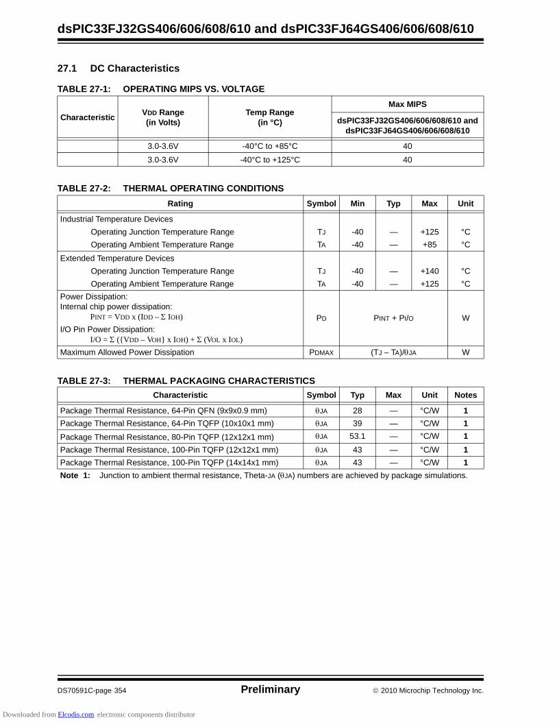
dsPIC33FJ32GS406/606/608/610 and dsPIC33FJ64GS406/606/608/610
DS70591C-page 354 Preliminary 2010 Microchip Technology Inc.
27.1 DC Characteristics
TABLE 27-1: OPERATING MIPS VS. VOLTAGE
CharacteristicVDD Range(in Volts)
Temp Range(in °C)
Max MIPS
dsPIC33FJ32GS406/606/608/610 and dsPIC33FJ64GS406/606/608/610
3.0-3.6V -40°C to +85°C 40
3.0-3.6V -40°C to +125°C 40
TABLE 27-2: THERMAL OPERATING CONDITIONS
Rating Symbol Min Typ Max Unit
Industrial Temperature Devices
Operating Junction Temperature Range TJ -40 — +125 °C
Operating Ambient Temperature Range TA -40 — +85 °C
Extended Temperature Devices
Operating Junction Temperature Range TJ -40 — +140 °C
Operating Ambient Temperature Range TA -40 — +125 °C
Power Dissipation:Internal chip power dissipation:
PINT = VDD x (IDD – IOH) PD PINT + PI/O WI/O Pin Power Dissipation:
I/O = ({VDD – VOH} x IOH) + (VOL x IOL)
Maximum Allowed Power Dissipation PDMAX (TJ – TA)/JA W
TABLE 27-3: THERMAL PACKAGING CHARACTERISTICS
Characteristic Symbol Typ Max Unit Notes
Package Thermal Resistance, 64-Pin QFN (9x9x0.9 mm) JA 28 — °C/W 1
Package Thermal Resistance, 64-Pin TQFP (10x10x1 mm) JA 39 — °C/W 1
Package Thermal Resistance, 80-Pin TQFP (12x12x1 mm) JA 53.1 — °C/W 1
Package Thermal Resistance, 100-Pin TQFP (12x12x1 mm) JA 43 — °C/W 1
Package Thermal Resistance, 100-Pin TQFP (14x14x1 mm) JA 43 — °C/W 1
Note 1: Junction to ambient thermal resistance, Theta-JA (JA) numbers are achieved by package simulations.
Downloaded from Elcodis.com electronic components distributor

2010 Microchip Technology Inc. Preliminary DS70591C-page 355
dsPIC33FJ32GS406/606/608/610 and dsPIC33FJ64GS406/606/608/610
TABLE 27-4: DC TEMPERATURE AND VOLTAGE SPECIFICATIONS
DC CHARACTERISTICS
Standard Operating Conditions: 3.0V to 3.6V(unless otherwise stated)Operating temperature -40°C TA +85°C for Industrial
-40°C TA +125°C for Extended
Param No.
Symbol Characteristic Min Typ(1) Max Units Conditions
Operating Voltage
DC10
Supply Voltage
VDD 3.0 — 3.6 V Industrial and extended
DC12 VDR RAM Data Retention Voltage(2) 1.8 — — V
DC16 VPOR VDD Start Voltage(4)
to Ensure Internal Power-on Reset Signal
— — VSS V
DC17 SVDD VDD Rise Rate(3)
to Ensure InternalPower-on Reset Signal
0.03 — — V/ms 0-3.0V in 0.1s
DC18 VCORE VDD Core Internal Regulator Voltage
2.25 — 2.75 V Voltage is dependent on load, temperature and VDD
Note 1: Data in “Typ” column is at 3.3V, +25°C unless otherwise stated.
2: This is the limit to which VDD may be lowered without losing RAM data.
3: These parameters are characterized but not tested in manufacturing.
4: VDD voltage must remain at Vss for a minimum of 200 µs to ensure POR.
Downloaded from Elcodis.com electronic components distributor
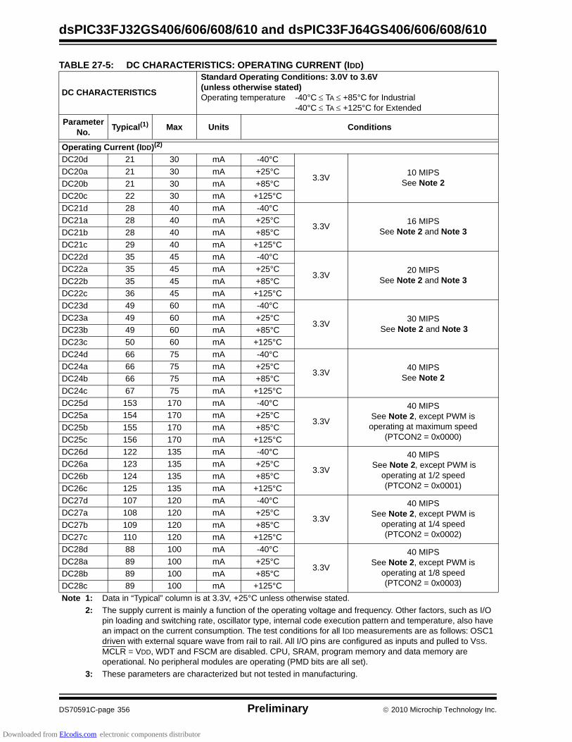
dsPIC33FJ32GS406/606/608/610 and dsPIC33FJ64GS406/606/608/610
DS70591C-page 356 Preliminary 2010 Microchip Technology Inc.
TABLE 27-5: DC CHARACTERISTICS: OPERATING CURRENT (IDD)
DC CHARACTERISTICS
Standard Operating Conditions: 3.0V to 3.6V(unless otherwise stated)Operating temperature -40°C TA +85°C for Industrial
-40°C TA +125°C for Extended
Parameter No.
Typical(1) Max Units Conditions
Operating Current (IDD)(2)
DC20d 21 30 mA -40°C
3.3V10 MIPS
See Note 2DC20a 21 30 mA +25°C
DC20b 21 30 mA +85°C
DC20c 22 30 mA +125°C
DC21d 28 40 mA -40°C
3.3V16 MIPS
See Note 2 and Note 3DC21a 28 40 mA +25°C
DC21b 28 40 mA +85°C
DC21c 29 40 mA +125°C
DC22d 35 45 mA -40°C
3.3V20 MIPS
See Note 2 and Note 3DC22a 35 45 mA +25°C
DC22b 35 45 mA +85°C
DC22c 36 45 mA +125°C
DC23d 49 60 mA -40°C
3.3V30 MIPS
See Note 2 and Note 3DC23a 49 60 mA +25°C
DC23b 49 60 mA +85°C
DC23c 50 60 mA +125°C
DC24d 66 75 mA -40°C
3.3V40 MIPS
See Note 2DC24a 66 75 mA +25°C
DC24b 66 75 mA +85°C
DC24c 67 75 mA +125°C
DC25d 153 170 mA -40°C
3.3V
40 MIPS
See Note 2, except PWM is operating at maximum speed
(PTCON2 = 0x0000)
DC25a 154 170 mA +25°C
DC25b 155 170 mA +85°C
DC25c 156 170 mA +125°C
DC26d 122 135 mA -40°C
3.3V
40 MIPS See Note 2, except PWM is
operating at 1/2 speed(PTCON2 = 0x0001)
DC26a 123 135 mA +25°C
DC26b 124 135 mA +85°C
DC26c 125 135 mA +125°C
DC27d 107 120 mA -40°C
3.3V
40 MIPSSee Note 2, except PWM is
operating at 1/4 speed(PTCON2 = 0x0002)
DC27a 108 120 mA +25°C
DC27b 109 120 mA +85°C
DC27c 110 120 mA +125°C
DC28d 88 100 mA -40°C
3.3V
40 MIPSSee Note 2, except PWM is
operating at 1/8 speed(PTCON2 = 0x0003)
DC28a 89 100 mA +25°C
DC28b 89 100 mA +85°C
DC28c 89 100 mA +125°C
Note 1: Data in “Typical” column is at 3.3V, +25°C unless otherwise stated.
2: The supply current is mainly a function of the operating voltage and frequency. Other factors, such as I/O pin loading and switching rate, oscillator type, internal code execution pattern and temperature, also have an impact on the current consumption. The test conditions for all IDD measurements are as follows: OSC1 driven with external square wave from rail to rail. All I/O pins are configured as inputs and pulled to VSS. MCLR = VDD, WDT and FSCM are disabled. CPU, SRAM, program memory and data memory are operational. No peripheral modules are operating (PMD bits are all set).
3: These parameters are characterized but not tested in manufacturing.
Downloaded from Elcodis.com electronic components distributor
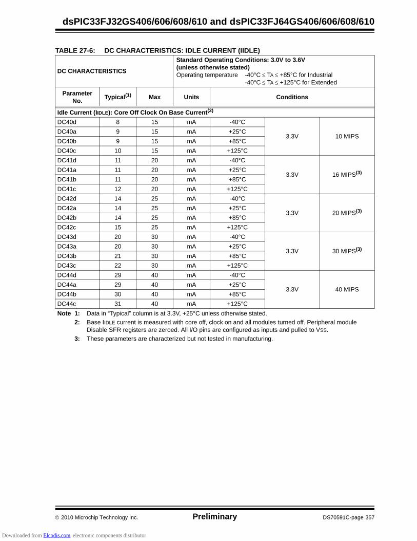
2010 Microchip Technology Inc. Preliminary DS70591C-page 357
dsPIC33FJ32GS406/606/608/610 and dsPIC33FJ64GS406/606/608/610
TABLE 27-6: DC CHARACTERISTICS: IDLE CURRENT (IIDLE)
DC CHARACTERISTICS
Standard Operating Conditions: 3.0V to 3.6V(unless otherwise stated)Operating temperature -40°C TA +85°C for Industrial
-40°C TA +125°C for Extended
Parameter No.
Typical(1) Max Units Conditions
Idle Current (IIDLE): Core Off Clock On Base Current(2)
DC40d 8 15 mA -40°C
3.3V 10 MIPSDC40a 9 15 mA +25°C
DC40b 9 15 mA +85°C
DC40c 10 15 mA +125°C
DC41d 11 20 mA -40°C
3.3V 16 MIPS(3)DC41a 11 mA +25°C20
DC41b 11 20 mA +85°C
DC41c 12 20 mA +125°C
DC42d 14 25 mA -40°C
3.3V 20 MIPS(3)DC42a 14 25 mA +25°C
DC42b 14 25 mA +85°C
DC42c 15 25 mA +125°C
DC43d 20 30 mA -40°C
3.3V 30 MIPS(3)DC43a 20 30 mA +25°C
DC43b 21 30 mA +85°C
DC43c 22 30 mA +125°C
DC44d 29 40 mA -40°C
3.3V 40 MIPSDC44a 29 40 mA +25°C
DC44b 30 40 mA +85°C
DC44c 31 40 mA +125°C
Note 1: Data in “Typical” column is at 3.3V, +25°C unless otherwise stated.
2: Base IIDLE current is measured with core off, clock on and all modules turned off. Peripheral module Disable SFR registers are zeroed. All I/O pins are configured as inputs and pulled to VSS.
3: These parameters are characterized but not tested in manufacturing.
Downloaded from Elcodis.com electronic components distributor

dsPIC33FJ32GS406/606/608/610 and dsPIC33FJ64GS406/606/608/610
DS70591C-page 358 Preliminary 2010 Microchip Technology Inc.
TABLE 27-7: DC CHARACTERISTICS: POWER-DOWN CURRENT (IPD)
DC CHARACTERISTICS
Standard Operating Conditions: 3.0V to 3.6V(unless otherwise stated)Operating temperature -40°C TA +85°C for Industrial
-40°C TA +125°C for Extended
Parameter No.
Typical(1) Max Units Conditions
Power-Down Current (IPD)(2,4)
DC60d 50 200 A -40°C
3.3V Base Power-Down CurrentDC60a 50 200 A +25°C
DC60b 200 500 A +85°C
DC60c 600 1000 A +125°C
DC61d 8 13 A -40°C
3.3V Watchdog Timer Current: IWDT(3)DC61a 10 15 A +25°C
DC61b 12 20 A +85°C
DC61c 13 25 A +125°C
Note 1: Data in the Typical column is at 3.3V, +25°C unless otherwise stated.
2: Base IPD is measured with all peripherals and clocks shut down. All I/Os are configured as inputs and pulled to VSS. WDT, etc., are all switched off, and VREGS (RCON<8>) = 1.
3: The current is the additional current consumed when the WDT module is enabled. This current should be added to the base IPD current.
4: These currents are measured on the device containing the most memory in this family.
TABLE 27-8: DC CHARACTERISTICS: DOZE CURRENT (IDOZE)
DC CHARACTERISTICS
Standard Operating Conditions: 3.0V to 3.6V(unless otherwise stated)Operating temperature -40°C TA +85°C for Industrial
-40°C TA +125°C for Extended
Parameter No. Typical(1) MaxDoze Ratio
Units Conditions
DC73a 105 120 1:2 mA
-40°C 3.3V 40 MIPSDC73f 82 100 1:64 mA
DC73g 82 100 1:128 mA
DC70a 105 120 1:2 mA
+25°C 3.3V 40 MIPSDC70f 80 100 1:64 mA
DC70g 79 100 1:128 mA
DC71a 105 120 1:2 mA
+85°C 3.3V 40 MIPSDC71f 77 100 1:64 mA
DC71g 77 100 1:128 mA
DC72a 105 120 1:2 mA
+125°C 3.3V 40 MIPSDC72f 76 100 1:64 mA
DC72g 76 100 1:128 mA
Note 1: Data in the Typical column is at 3.3V, +25°C unless otherwise stated.
Downloaded from Elcodis.com electronic components distributor
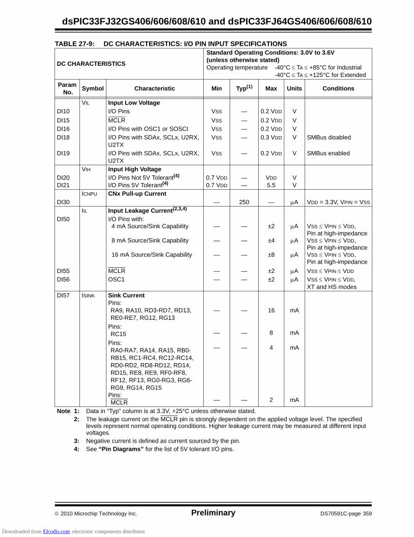
2010 Microchip Technology Inc. Preliminary DS70591C-page 359
dsPIC33FJ32GS406/606/608/610 and dsPIC33FJ64GS406/606/608/610
TABLE 27-9: DC CHARACTERISTICS: I/O PIN INPUT SPECIFICATIONS
DC CHARACTERISTICS
Standard Operating Conditions: 3.0V to 3.6V(unless otherwise stated)Operating temperature -40°C TA +85°C for Industrial
-40°C TA +125°C for Extended
Param No.
Symbol Characteristic Min Typ(1) Max Units Conditions
VIL Input Low Voltage
DI10 I/O Pins VSS — 0.2 VDD V
DI15 MCLR VSS — 0.2 VDD VDI16 I/O Pins with OSC1 or SOSCI VSS — 0.2 VDD V
DI18 I/O Pins with SDAx, SCLx, U2RX, U2TX
VSS — 0.3 VDD V SMBus disabled
DI19 I/O Pins with SDAx, SCLx, U2RX, U2TX
VSS — 0.2 VDD V SMBus enabled
VIH Input High VoltageDI20DI21
I/O Pins Not 5V Tolerant(4)
I/O Pins 5V Tolerant(4)0.7 VDD
0.7 VDD
——
VDD
5.5VV
ICNPU CNx Pull-up CurrentDI30 — 250 — A VDD = 3.3V, VPIN = VSS
IIL Input Leakage Current(2,3,4)
DI50 I/O Pins with: 4 mA Source/Sink Capability
8 mA Source/Sink Capability
16 mA Source/Sink Capability
—
—
—
—
—
—
±2
±4
±8
A
A
A
VSS VPIN VDD,Pin at high-impedanceVSS VPIN VDD,Pin at high-impedanceVSS VPIN VDD,Pin at high-impedance
DI55 MCLR — — ±2 A VSS VPIN VDD
DI56 OSC1 — — ±2 A VSS VPIN VDD, XT and HS modes
DI57 ISINK Sink CurrentPins:RA9, RA10, RD3-RD7, RD13, RE0-RE7, RG12, RG13
Pins:RC15
Pins:RA0-RA7, RA14, RA15, RB0-RB15, RC1-RC4, RC12-RC14, RD0-RD2, RD8-RD12, RD14, RD15, RE8, RE9, RF0-RF8, RF12, RF13, RG0-RG3, RG6-RG9, RG14, RG15
Pins:MCLR
—
—
—
—
—
—
—
—
16
8
4
2
mA
mA
mA
mA
Note 1: Data in “Typ” column is at 3.3V, +25°C unless otherwise stated.2: The leakage current on the MCLR pin is strongly dependent on the applied voltage level. The specified
levels represent normal operating conditions. Higher leakage current may be measured at different input voltages.
3: Negative current is defined as current sourced by the pin.4: See “Pin Diagrams” for the list of 5V tolerant I/O pins.
Downloaded from Elcodis.com electronic components distributor

dsPIC33FJ32GS406/606/608/610 and dsPIC33FJ64GS406/606/608/610
DS70591C-page 360 Preliminary 2010 Microchip Technology Inc.
TABLE 27-10: DC CHARACTERISTICS: I/O PIN OUTPUT SPECIFICATIONS
DC CHARACTERISTICS
Standard Operating Conditions: 3.0V to 3.6V(unless otherwise stated)Operating temperature -40°C TA +85°C for Industrial
-40°C TA +125°C for Extended
Param No.
Symbol Characteristic Min Typ Max Units Conditions
DO10 VOL Output Low Voltage
I/O Ports:4 mA Source/Sink Capability8 mA Source/Sink Capability16 mA Source/Sink Capability
———
———
0.40.40.4
VVV
IOL = 4 mA, VDD = 3.3VIOL = 8 mA, VDD = 3.3VIOL = 16 mA, VDD = 3.3V
DO16 OSC2/CLKO — — 0.4 V IOL = 2 mA, VDD = 3.3V
DO20 VOH Output High Voltage
I/O Ports:4 mA Source/Sink Capability8 mA Source/Sink Capability16 mA Source/Sink Capability
2.402.402.40
———
———
VVV
IOH = -4 mA, VDD = 3.3VIOH = -8 mA, VDD = 3.3VIOH = -16 mA, VDD = 3.3V
DO26 OSC2/CLKO 2.41 — — V IOH = -1.3 mA, VDD = 3.3V
DO27 ISOURCE Source CurrentPins:RA9, RA10, RD3-RD7, RD13, RE0-RE7, RG12, RG13
Pins:RC15
Pins:RA0-RA7, RA14, RA15, RB0-RB15, RC1-RC4, RC12-RC14, RD0-RD2, RD8-RD12, RD14, RD15, RE8, RE9, RF0-RF8, RF12, RF13, RG0-RG3, RG6-RG9, RG14, RG15
Pins:MCLR
—
—
—
—
—
—
—
—
16
8
4
2
mA
mA
mA
mA
TABLE 27-11: ELECTRICAL CHARACTERISTICS: BOR
DC CHARACTERISTICS
Standard Operating Conditions: 3.0V to 3.6V(unless otherwise stated)Operating temperature -40°C TA +85°C for Industrial
-40°C TA +125°C for Extended
ParamNo.
Symbol Characteristic Min(1) Typ Max Units Conditions
BO10 VBOR BOR Event on VDD Transition High-to-LowBOR Event is Tied to VDD Core Voltage Decrease
2.6 — 2.95 V
Note 1: Parameters are for design guidance only and are not tested in manufacturing.
Downloaded from Elcodis.com electronic components distributor
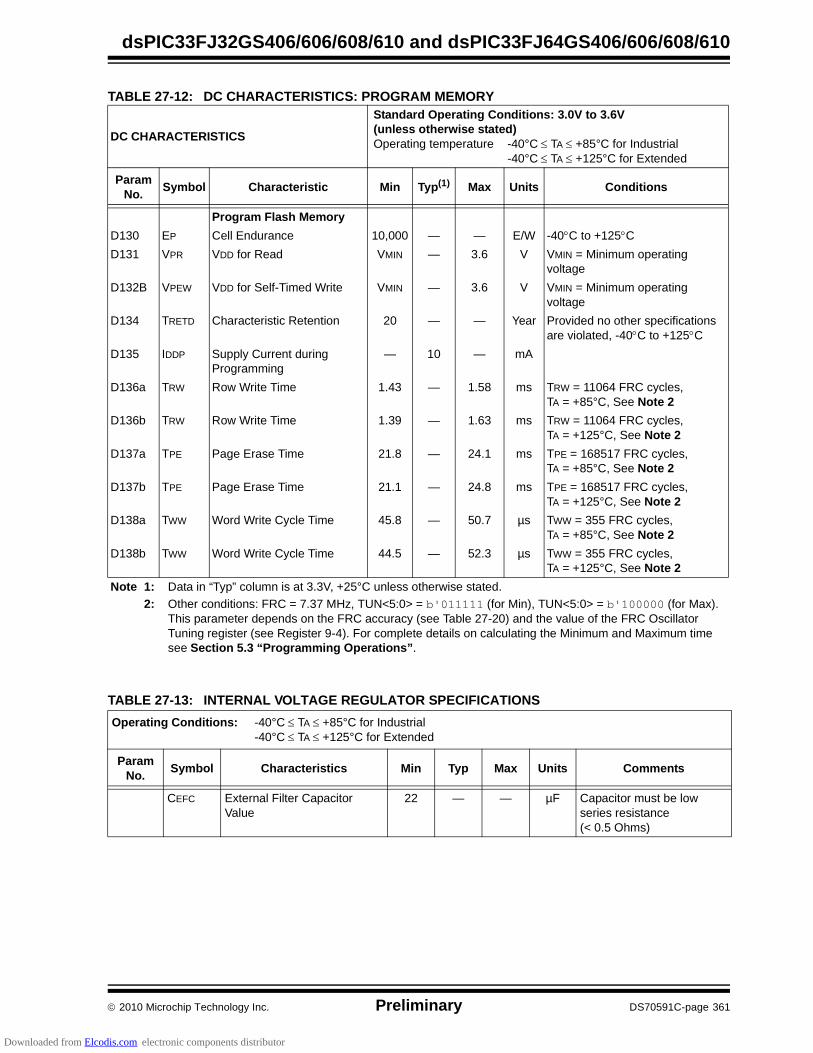
2010 Microchip Technology Inc. Preliminary DS70591C-page 361
dsPIC33FJ32GS406/606/608/610 and dsPIC33FJ64GS406/606/608/610
TABLE 27-13: INTERNAL VOLTAGE REGULATOR SPECIFICATIONS
TABLE 27-12: DC CHARACTERISTICS: PROGRAM MEMORY
DC CHARACTERISTICS
Standard Operating Conditions: 3.0V to 3.6V(unless otherwise stated)Operating temperature -40°C TA +85°C for Industrial
-40°C TA +125°C for Extended
ParamNo.
Symbol Characteristic Min Typ(1) Max Units Conditions
Program Flash Memory
D130 EP Cell Endurance 10,000 — — E/W -40C to +125C
D131 VPR VDD for Read VMIN — 3.6 V VMIN = Minimum operating voltage
D132B VPEW VDD for Self-Timed Write VMIN — 3.6 V VMIN = Minimum operating voltage
D134 TRETD Characteristic Retention 20 — — Year Provided no other specifications are violated, -40C to +125C
D135 IDDP Supply Current during Programming
— 10 — mA
D136a TRW Row Write Time 1.43 — 1.58 ms TRW = 11064 FRC cycles, TA = +85°C, See Note 2
D136b TRW Row Write Time 1.39 — 1.63 ms TRW = 11064 FRC cycles, TA = +125°C, See Note 2
D137a TPE Page Erase Time 21.8 — 24.1 ms TPE = 168517 FRC cycles, TA = +85°C, See Note 2
D137b TPE Page Erase Time 21.1 — 24.8 ms TPE = 168517 FRC cycles, TA = +125°C, See Note 2
D138a TWW Word Write Cycle Time 45.8 — 50.7 µs TWW = 355 FRC cycles, TA = +85°C, See Note 2
D138b TWW Word Write Cycle Time 44.5 — 52.3 µs TWW = 355 FRC cycles, TA = +125°C, See Note 2
Note 1: Data in “Typ” column is at 3.3V, +25°C unless otherwise stated.
2: Other conditions: FRC = 7.37 MHz, TUN<5:0> = b'011111 (for Min), TUN<5:0> = b'100000 (for Max). This parameter depends on the FRC accuracy (see Table 27-20) and the value of the FRC Oscillator Tuning register (see Register 9-4). For complete details on calculating the Minimum and Maximum time see Section 5.3 “Programming Operations”.
Operating Conditions: -40°C TA +85°C for Industrial-40°C TA +125°C for Extended
ParamNo.
Symbol Characteristics Min Typ Max Units Comments
CEFC External Filter Capacitor Value
22 — — µF Capacitor must be low series resistance (< 0.5 Ohms)
Downloaded from Elcodis.com electronic components distributor
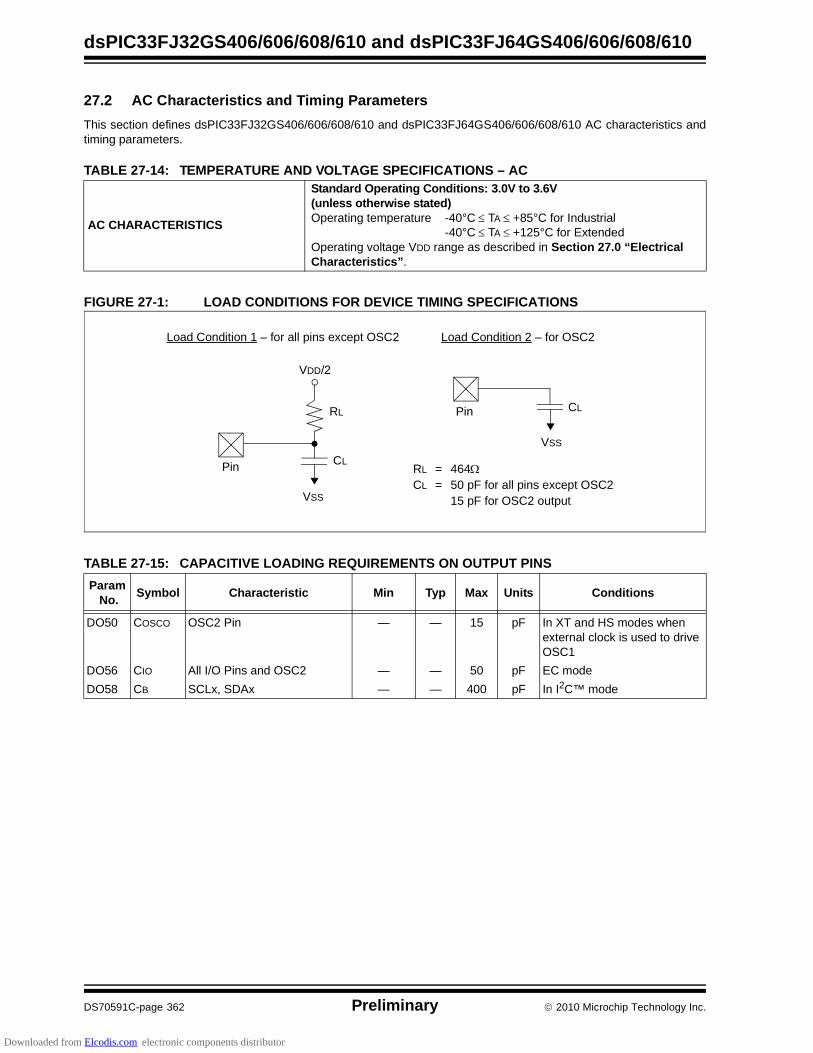
dsPIC33FJ32GS406/606/608/610 and dsPIC33FJ64GS406/606/608/610
DS70591C-page 362 Preliminary 2010 Microchip Technology Inc.
27.2 AC Characteristics and Timing Parameters
This section defines dsPIC33FJ32GS406/606/608/610 and dsPIC33FJ64GS406/606/608/610 AC characteristics andtiming parameters.
TABLE 27-14: TEMPERATURE AND VOLTAGE SPECIFICATIONS – AC
FIGURE 27-1: LOAD CONDITIONS FOR DEVICE TIMING SPECIFICATIONS
TABLE 27-15: CAPACITIVE LOADING REQUIREMENTS ON OUTPUT PINS
AC CHARACTERISTICS
Standard Operating Conditions: 3.0V to 3.6V(unless otherwise stated)Operating temperature -40°C TA +85°C for Industrial
-40°C TA +125°C for ExtendedOperating voltage VDD range as described in Section 27.0 “Electrical Characteristics”.
Param No.
Symbol Characteristic Min Typ Max Units Conditions
DO50 COSCO OSC2 Pin — — 15 pF In XT and HS modes when external clock is used to drive OSC1
DO56 CIO All I/O Pins and OSC2 — — 50 pF EC mode
DO58 CB SCLx, SDAx — — 400 pF In I2C™ mode
VDD/2
CL
RL
Pin
Pin
VSS
VSS
CL
RL = 464CL = 50 pF for all pins except OSC2
15 pF for OSC2 output
Load Condition 1 – for all pins except OSC2 Load Condition 2 – for OSC2
Downloaded from Elcodis.com electronic components distributor

2010 Microchip Technology Inc. Preliminary DS70591C-page 363
dsPIC33FJ32GS406/606/608/610 and dsPIC33FJ64GS406/606/608/610
FIGURE 27-2: EXTERNAL CLOCK TIMING
Q1 Q2 Q3 Q4
OSC1
CLKO
Q1 Q2 Q3 Q4
OS20
OS25OS30 OS30
OS40OS41
OS31 OS31
TABLE 27-16: EXTERNAL CLOCK TIMING REQUIREMENTS
AC CHARACTERISTICS
Standard Operating Conditions: 3.0V to 3.6V(unless otherwise stated)Operating temperature -40°C TA +85°C for Industrial
-40°C TA +125°C for Extended
ParamNo.
Symb Characteristic Min Typ(1) Max Units Conditions
OS10 FIN External CLKI Frequency(External clocks allowed onlyin EC and ECPLL modes)
DC — 40 MHz EC
Oscillator Crystal Frequency 3.510
——
1040
MHzMHz
XTHS
OS20 TOSC TOSC = 1/FOSC 12.5 — DC ns
OS25 TCY Instruction Cycle Time(2) 25 — DC ns
OS30 TosL,TosH
External Clock in (OSC1)High or Low Time
0.375 x TOSC — 0.625 x TOSC ns EC
OS31 TosR,TosF
External Clock in (OSC1)Rise or Fall Time
— — 20 ns EC
OS40 TckR CLKO Rise Time(3) — 5.2 — ns
OS41 TckF CLKO Fall Time(3) — 5.2 — ns
Note 1: Data in “Typ” column is at 3.3V, +25°C unless otherwise stated.
2: Instruction cycle period (TCY) equals two times the input oscillator time-base period. All specified values are based on characterization data for that particular oscillator type under standard operating conditions with the device executing code. Exceeding these specified limits may result in an unstable oscillator operation and/or higher than expected current consumption. All devices are tested to operate at “min.” values with an external clock applied to the OSC1/CLKI pin. When an external clock input is used, the “max.” cycle time limit is “DC” (no clock) for all devices.
3: Measurements are taken in EC mode. The CLKO signal is measured on the OSC2 pin.
Downloaded from Elcodis.com electronic components distributor
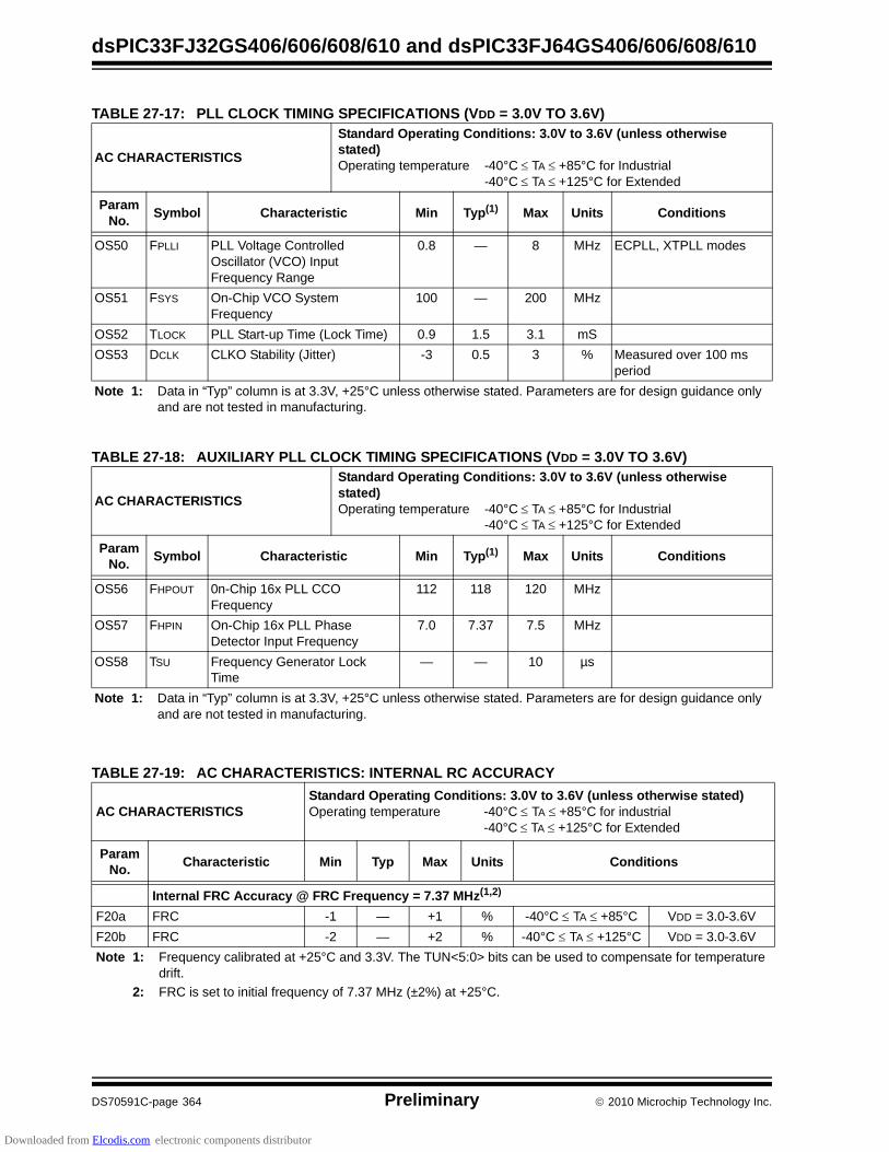
dsPIC33FJ32GS406/606/608/610 and dsPIC33FJ64GS406/606/608/610
DS70591C-page 364 Preliminary 2010 Microchip Technology Inc.
TABLE 27-17: PLL CLOCK TIMING SPECIFICATIONS (VDD = 3.0V TO 3.6V)
AC CHARACTERISTICS
Standard Operating Conditions: 3.0V to 3.6V (unless otherwise stated)Operating temperature -40°C TA +85°C for Industrial
-40°C TA +125°C for Extended
ParamNo.
Symbol Characteristic Min Typ(1) Max Units Conditions
OS50 FPLLI PLL Voltage Controlled Oscillator (VCO) Input Frequency Range
0.8 — 8 MHz ECPLL, XTPLL modes
OS51 FSYS On-Chip VCO System Frequency
100 — 200 MHz
OS52 TLOCK PLL Start-up Time (Lock Time) 0.9 1.5 3.1 mS
OS53 DCLK CLKO Stability (Jitter) -3 0.5 3 % Measured over 100 ms period
Note 1: Data in “Typ” column is at 3.3V, +25°C unless otherwise stated. Parameters are for design guidance only and are not tested in manufacturing.
TABLE 27-18: AUXILIARY PLL CLOCK TIMING SPECIFICATIONS (VDD = 3.0V TO 3.6V)
AC CHARACTERISTICS
Standard Operating Conditions: 3.0V to 3.6V (unless otherwise stated)Operating temperature -40°C TA +85°C for Industrial
-40°C TA +125°C for Extended
ParamNo.
Symbol Characteristic Min Typ(1) Max Units Conditions
OS56 FHPOUT 0n-Chip 16x PLL CCO Frequency
112 118 120 MHz
OS57 FHPIN On-Chip 16x PLL Phase Detector Input Frequency
7.0 7.37 7.5 MHz
OS58 TSU Frequency Generator Lock Time
— — 10 µs
Note 1: Data in “Typ” column is at 3.3V, +25°C unless otherwise stated. Parameters are for design guidance only and are not tested in manufacturing.
TABLE 27-19: AC CHARACTERISTICS: INTERNAL RC ACCURACY
AC CHARACTERISTICSStandard Operating Conditions: 3.0V to 3.6V (unless otherwise stated)Operating temperature -40°C TA +85°C for industrial
-40°C TA +125°C for Extended
Param No.
Characteristic Min Typ Max Units Conditions
Internal FRC Accuracy @ FRC Frequency = 7.37 MHz(1,2)
F20a FRC -1 — +1 % -40°C TA +85°C VDD = 3.0-3.6V
F20b FRC -2 — +2 % -40°C TA +125°C VDD = 3.0-3.6V
Note 1: Frequency calibrated at +25°C and 3.3V. The TUN<5:0> bits can be used to compensate for temperature drift.
2: FRC is set to initial frequency of 7.37 MHz (±2%) at +25°C.
Downloaded from Elcodis.com electronic components distributor

2010 Microchip Technology Inc. Preliminary DS70591C-page 365
dsPIC33FJ32GS406/606/608/610 and dsPIC33FJ64GS406/606/608/610
FIGURE 27-3: I/O TIMING CHARACTERISTICS
TABLE 27-20: INTERNAL RC ACCURACY
AC CHARACTERISTICSStandard Operating Conditions: 3.0V to 3.6V (unless otherwise stated)Operating temperature -40°C TA +85°C for Industrial
-40°C TA +125°C for Extended
ParamNo.
Characteristic Min Typ Max Units Conditions
LPRC @ 32.768 kHz(1)
F21a LPRC -40 — +40 % -40°C TA +85°C
F21b LPRC -70 — +70 % -40°C TA +125°C
Note 1: Change of LPRC frequency as VDD changes.
Note: Refer to Figure 27-1 for load conditions.
I/O Pin(Input)
I/O Pin(Output)
DI35
Old Value New Value
DI40
DO31DO32
TABLE 27-21: I/O TIMING REQUIREMENTS
AC CHARACTERISTICS
Standard Operating Conditions: 3.0V to 3.6V(unless otherwise stated)Operating temperature -40°C TA +85°C for Industrial
-40°C TA +125°C for Extended
ParamNo.
Symbol Characteristic Min Typ(1) Max Units Conditions
DO31 TIOR Port Output Rise Time — 10 25 ns Refer to Figure 27-1 for test conditions
DO32 TIOF Port Output Fall Time — 10 25 ns Refer to Figure 27-1 for test conditions
DI35 TINP INTx Pin High or Low Time (output) 20 — — ns
DI40 TRBP CNx High or Low Time (input) 2 — — TCY
Note 1: Data in “Typ” column is at 3.3V, +25°C unless otherwise stated.
Downloaded from Elcodis.com electronic components distributor

dsPIC33FJ32GS406/606/608/610 and dsPIC33FJ64GS406/606/608/610
DS70591C-page 366 Preliminary 2010 Microchip Technology Inc.
FIGURE 27-4: RESET, WATCHDOG TIMER, OSCILLATOR START-UP TIMER AND POWER-UP TIMER TIMING CHARACTERISTICS
VDD
MCLR
InternalPOR
PWRTTime-out
OSCTime-out
InternalReset
WatchdogTimerReset
SY11
SY10
SY20SY13
I/O Pins
SY13
Note: Refer to Figure 27-1 for load conditions.
FSCM Delay
SY35
SY30
SY12
Downloaded from Elcodis.com electronic components distributor

2010 Microchip Technology Inc. Preliminary DS70591C-page 367
dsPIC33FJ32GS406/606/608/610 and dsPIC33FJ64GS406/606/608/610
TABLE 27-22: RESET, WATCHDOG TIMER, OSCILLATOR START-UP TIMER, POWER-UP TIMER TIMING REQUIREMENTS
AC CHARACTERISTICS
Standard Operating Conditions: 3.0V to 3.6V(unless otherwise stated)Operating temperature -40°C TA +85°C for Industrial
-40°C TA +125°C for Extended
ParamNo.
Symbol Characteristic(1) Min Typ(2) Max Units Conditions
SY10 TMCL MCLR Pulse Width (low) 2 — — s -40°C to +85°C
SY11 TPWRT Power-up Timer Period — 248163264
128
— ms -40°C to +85°CUser programmable
SY12 TPOR Power-on Reset Delay 3 10 30 s -40°C to +85°C
SY13 TIOZ I/O High-Impedance from MCLR Low or Watchdog Timer Reset
0.68 0.72 1.2 s
SY20 TWDT1 Watchdog Timer Time-out Period — — — ms See Section 24.4 “Watch-dog Timer (WDT)” and LPRC parameter F21a (Table 27-20).
SY30 TOST Oscillator Start-up Time — 1024TOSC
— — TOSC = OSC1 period
Note 1: These parameters are characterized but not tested in manufacturing. 2: Data in “Typ” column is at 3.3V, +25°C unless otherwise stated.
Downloaded from Elcodis.com electronic components distributor
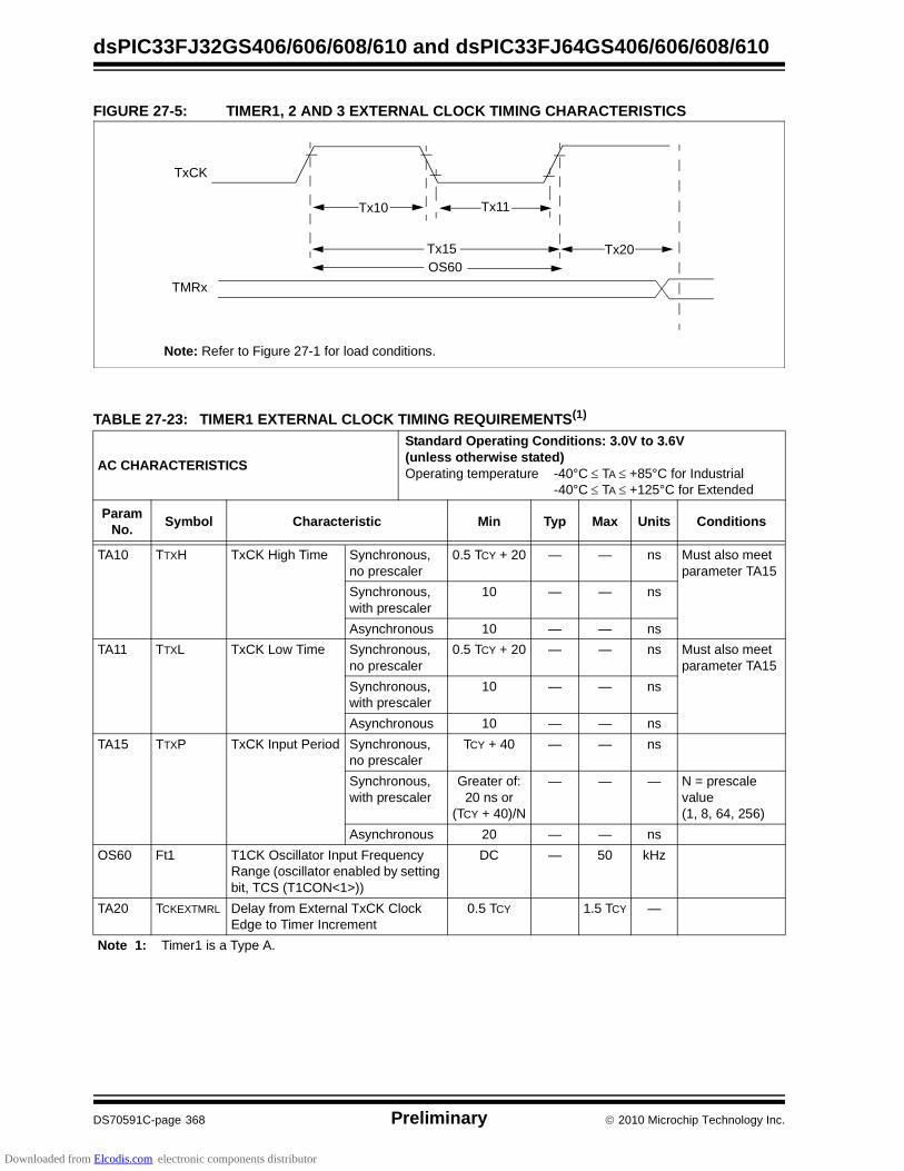
dsPIC33FJ32GS406/606/608/610 and dsPIC33FJ64GS406/606/608/610
DS70591C-page 368 Preliminary 2010 Microchip Technology Inc.
FIGURE 27-5: TIMER1, 2 AND 3 EXTERNAL CLOCK TIMING CHARACTERISTICS
Note: Refer to Figure 27-1 for load conditions.
Tx11
Tx15
Tx10
Tx20
TMRx
OS60
TxCK
TABLE 27-23: TIMER1 EXTERNAL CLOCK TIMING REQUIREMENTS(1)
AC CHARACTERISTICS
Standard Operating Conditions: 3.0V to 3.6V(unless otherwise stated)Operating temperature -40°C TA +85°C for Industrial
-40°C TA +125°C for Extended
ParamNo.
Symbol Characteristic Min Typ Max Units Conditions
TA10 TTXH TxCK High Time Synchronous,no prescaler
0.5 TCY + 20 — — ns Must also meet parameter TA15
Synchronous,with prescaler
10 — — ns
Asynchronous 10 — — ns
TA11 TTXL TxCK Low Time Synchronous,no prescaler
0.5 TCY + 20 — — ns Must also meet parameter TA15
Synchronous,with prescaler
10 — — ns
Asynchronous 10 — — ns
TA15 TTXP TxCK Input Period Synchronous,no prescaler
TCY + 40 — — ns
Synchronous,with prescaler
Greater of:20 ns or
(TCY + 40)/N
— — — N = prescale value(1, 8, 64, 256)
Asynchronous 20 — — ns
OS60 Ft1 T1CK Oscillator Input Frequency Range (oscillator enabled by setting bit, TCS (T1CON<1>))
DC — 50 kHz
TA20 TCKEXTMRL Delay from External TxCK Clock Edge to Timer Increment
0.5 TCY 1.5 TCY —
Note 1: Timer1 is a Type A.
Downloaded from Elcodis.com electronic components distributor

2010 Microchip Technology Inc. Preliminary DS70591C-page 369
dsPIC33FJ32GS406/606/608/610 and dsPIC33FJ64GS406/606/608/610
TABLE 27-24: TIMER2 EXTERNAL CLOCK TIMING REQUIREMENTS
AC CHARACTERISTICS
Standard Operating Conditions: 3.0V to 3.6V(unless otherwise stated)Operating temperature -40°C TA +85°C for Industrial
-40°C TA +125°C for Extended
ParamNo.
Symbol Characteristic Min Typ Max Units Conditions
TB10 TTXH TxCK High Time Synchronous,no prescaler
0.5 TCY + 20 — — ns Must also meet parameter TB15
Synchronous,with prescaler
10 — — ns
TB11 TTXL TxCK Low Time Synchronous,no prescaler
0.5 TCY + 20 — — ns Must also meet parameter TB15
Synchronous,with prescaler
10 — — ns
TB15 TTXP TxCK Input Period
Synchronous,no prescaler
TCY + 40 — — ns N = prescale value(1, 8, 64, 256)Synchronous,
with prescalerGreater of:
20 ns or(TCY + 40)/N
TB20 TCKEXTMRL Delay from External TxCK Clock Edge to Timer Increment
0.5 TCY — 1.5 TCY —
TABLE 27-25: TIMER3 EXTERNAL CLOCK TIMING REQUIREMENTS
AC CHARACTERISTICS
Standard Operating Conditions: 3.0V to 3.6V(unless otherwise stated)Operating temperature -40°C TA +85°C for Industrial
-40°C TA +125°C for Extended
ParamNo.
Symbol Characteristic Min Typ Max Units Conditions
TC10 TTXH TxCK High Time Synchronous 0.5 TCY + 20 — — ns Must also meet parameter TC15
TC11 TTXL TxCK Low Time Synchronous 0.5 TCY + 20 — — ns Must also meet parameter TC15
TC15 TTXP TxCK Input Period Synchronous,no prescaler
TCY + 40 — — ns N = prescalevalue (1, 8, 64, 256)Synchronous,
with prescalerGreater of:
20 ns or (TCY + 40)/N
TC20 TCKEXTMRL Delay from External TxCK Clock Edge to Timer Increment
0.5 TCY — 1.5 TCY
—
Downloaded from Elcodis.com electronic components distributor

dsPIC33FJ32GS406/606/608/610 and dsPIC33FJ64GS406/606/608/610
DS70591C-page 370 Preliminary 2010 Microchip Technology Inc.
FIGURE 27-6: INPUT CAPTURE (CAPx) TIMING CHARACTERISTICS
FIGURE 27-7: OUTPUT COMPARE MODULE (OCx) TIMING CHARACTERISTICS
TABLE 27-26: INPUT CAPTURE TIMING REQUIREMENTS
AC CHARACTERISTICS
Standard Operating Conditions: 3.0V to 3.6V(unless otherwise stated)Operating temperature -40°C TA +85°C for Industrial
-40°C TA +125°C for Extended
ParamNo.
Symbol Characteristic(1) Min Max Units Conditions
IC10 TccL ICx Input Low Time No prescaler 0.5 TCY + 20 — ns
With prescaler 10 — ns
IC11 TccH ICx Input High Time No prescaler 0.5 TCY + 20 — ns
With prescaler 10 — ns
IC15 TccP ICx Input Period (TCY + 40)/N — ns N = prescale value (1, 4, 16)
Note 1: These parameters are characterized but not tested in manufacturing.
TABLE 27-27: OUTPUT COMPARE MODULE TIMING REQUIREMENTS
AC CHARACTERISTICS
Standard Operating Conditions: 3.0V to 3.6V(unless otherwise stated)Operating temperature -40°C TA +85°C for Industrial
-40°C TA +125°C for Extended
Param No.
Symbol Characteristic(1) Min Typ Max Units Conditions
OC10 TccF OCx Output Fall Time — — — ns See parameter D032
OC11 TccR OCx Output Rise Time — — — ns See parameter D031
Note 1: These parameters are characterized but not tested in manufacturing.
ICx
IC10 IC11
IC15
Note: Refer to Figure 27-1 for load conditions.
OCx
OC11 OC10(Output Compare
Note: Refer to Figure 27-1 for load conditions.
or PWM Mode)
Downloaded from Elcodis.com electronic components distributor

2010 Microchip Technology Inc. Preliminary DS70591C-page 371
dsPIC33FJ32GS406/606/608/610 and dsPIC33FJ64GS406/606/608/610
FIGURE 27-8: OC/PWM MODULE TIMING CHARACTERISTICS
OCFA
OCx
OC20
OC15
TABLE 27-28: SIMPLE OC/PWM MODE TIMING REQUIREMENTS
AC CHARACTERISTICS
Standard Operating Conditions: 3.0V to 3.6V(unless otherwise stated)Operating temperature -40°C TA +85°C for Industrial
-40°C TA +125°C for Extended
Param No.
Symbol Characteristic(1) Min Typ Max Units Conditions
OC15 TFD Fault Input to PWM I/O Change
— — 50 ns
OC20 TFLT Fault Input Pulse Width 50 — — ns
Note 1: These parameters are characterized but not tested in manufacturing.
Downloaded from Elcodis.com electronic components distributor

dsPIC33FJ32GS406/606/608/610 and dsPIC33FJ64GS406/606/608/610
DS70591C-page 372 Preliminary 2010 Microchip Technology Inc.
FIGURE 27-9: HIGH-SPEED PWM MODULE FAULT TIMING CHARACTERISTICS
FIGURE 27-10: HIGH-SPEED PWM MODULE TIMING CHARACTERISTICS
FLTx
PWMx
MP30
MP20
PWMx
MP11 MP10
Note: Refer to Figure 27-1 for load conditions.
TABLE 27-29: HIGH-SPEED PWM MODULE TIMING REQUIREMENTS
AC CHARACTERISTICS
Standard Operating Conditions: 3.0V to 3.6V(unless otherwise stated)Operating temperature -40°C TA +85°C for Industrial
-40°C TA +125°C for Extended
ParamNo.
Symbol Characteristic(1) Min Typ Max Units Conditions
MP10 TFPWM PWM Output Fall Time — 2.5 — ns
MP11 TRPWM PWM Output Rise Time — 2.5 — ns
MP20TFD Fault Input to PWM
I/O Change— — 15 ns DTC<10> = 10
MP30 TFH Minimum PWM Fault Pulse Width 8 — — ns
MP31 TPDLY Tap Delay 1.04 — — ns ACLK = 120 MHz
MP32 ACLK PWM Input Clock — — 120 MHz See Note 2
Note 1: These parameters are characterized but not tested in manufacturing.
2: This parameter is a maximum allowed input clock for the PWM module.
Downloaded from Elcodis.com electronic components distributor
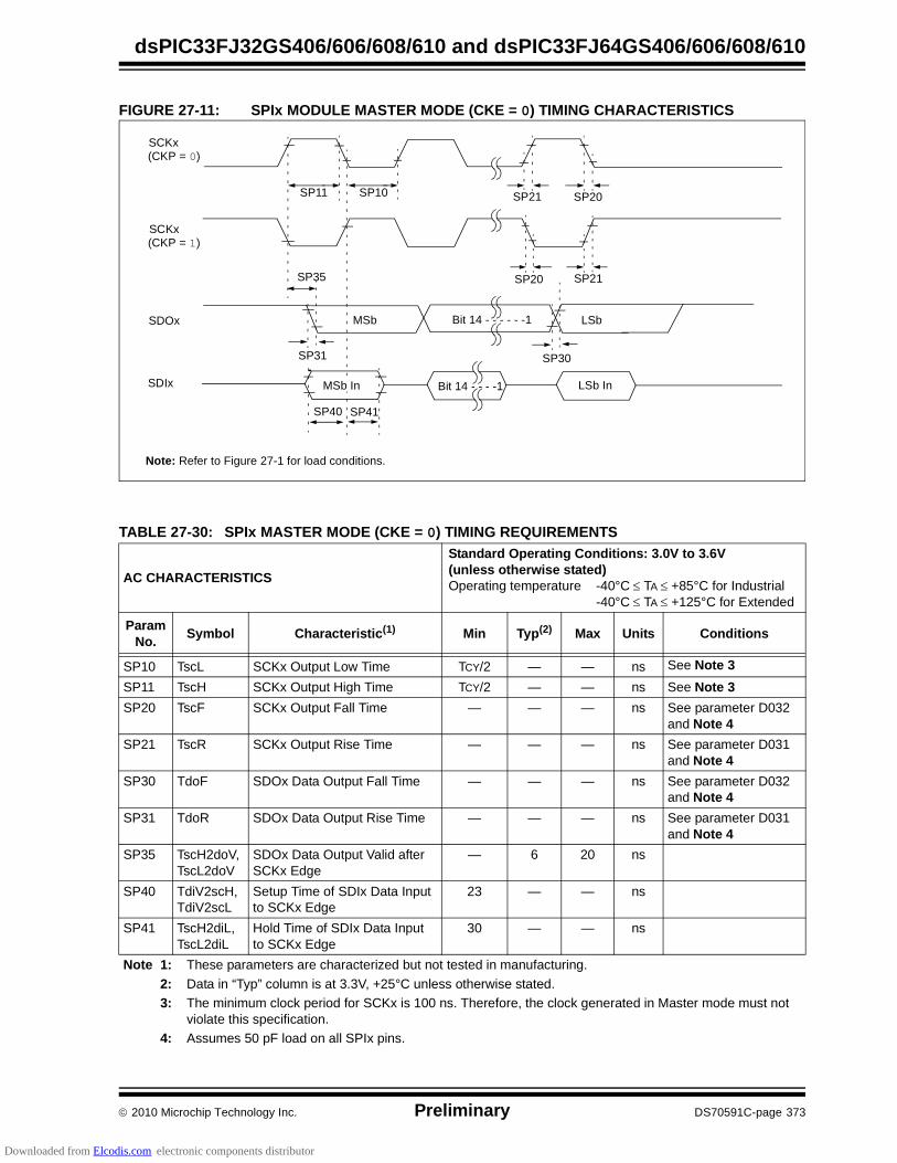
2010 Microchip Technology Inc. Preliminary DS70591C-page 373
dsPIC33FJ32GS406/606/608/610 and dsPIC33FJ64GS406/606/608/610
FIGURE 27-11: SPIx MODULE MASTER MODE (CKE = 0) TIMING CHARACTERISTICS
SCKx(CKP = 0)
SCKx(CKP = 1)
SDOx
SDIx
SP11 SP10
SP40 SP41
SP21SP20SP35
SP20SP21
MSb LSbBit 14 - - - - - -1
LSb InBit 14 - - - -1
SP30SP31
Note: Refer to Figure 27-1 for load conditions.
MSb In
TABLE 27-30: SPIx MASTER MODE (CKE = 0) TIMING REQUIREMENTS
AC CHARACTERISTICS
Standard Operating Conditions: 3.0V to 3.6V(unless otherwise stated)Operating temperature -40°C TA +85°C for Industrial
-40°C TA +125°C for Extended
ParamNo.
Symbol Characteristic(1) Min Typ(2) Max Units Conditions
SP10 TscL SCKx Output Low Time TCY/2 — — ns See Note 3
SP11 TscH SCKx Output High Time TCY/2 — — ns See Note 3
SP20 TscF SCKx Output Fall Time — — — ns See parameter D032 and Note 4
SP21 TscR SCKx Output Rise Time — — — ns See parameter D031 and Note 4
SP30 TdoF SDOx Data Output Fall Time — — — ns See parameter D032 and Note 4
SP31 TdoR SDOx Data Output Rise Time — — — ns See parameter D031 and Note 4
SP35 TscH2doV,TscL2doV
SDOx Data Output Valid after SCKx Edge
— 6 20 ns
SP40 TdiV2scH,TdiV2scL
Setup Time of SDIx Data Inputto SCKx Edge
23 — — ns
SP41 TscH2diL,TscL2diL
Hold Time of SDIx Data Inputto SCKx Edge
30 — — ns
Note 1: These parameters are characterized but not tested in manufacturing.
2: Data in “Typ” column is at 3.3V, +25°C unless otherwise stated.
3: The minimum clock period for SCKx is 100 ns. Therefore, the clock generated in Master mode must not violate this specification.
4: Assumes 50 pF load on all SPIx pins.
Downloaded from Elcodis.com electronic components distributor
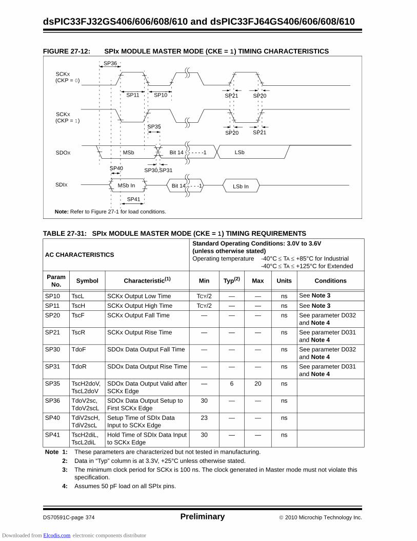
dsPIC33FJ32GS406/606/608/610 and dsPIC33FJ64GS406/606/608/610
DS70591C-page 374 Preliminary 2010 Microchip Technology Inc.
FIGURE 27-12: SPIx MODULE MASTER MODE (CKE = 1) TIMING CHARACTERISTICS
TABLE 27-31: SPIx MODULE MASTER MODE (CKE = 1) TIMING REQUIREMENTS
AC CHARACTERISTICS
Standard Operating Conditions: 3.0V to 3.6V(unless otherwise stated)Operating temperature -40°C TA +85°C for Industrial
-40°C TA +125°C for Extended
ParamNo.
Symbol Characteristic(1) Min Typ(2) Max Units Conditions
SP10 TscL SCKx Output Low Time TCY/2 — — ns See Note 3
SP11 TscH SCKx Output High Time TCY/2 — — ns See Note 3
SP20 TscF SCKx Output Fall Time — — — ns See parameter D032 and Note 4
SP21 TscR SCKx Output Rise Time — — — ns See parameter D031 and Note 4
SP30 TdoF SDOx Data Output Fall Time — — — ns See parameter D032 and Note 4
SP31 TdoR SDOx Data Output Rise Time — — — ns See parameter D031 and Note 4
SP35 TscH2doV,TscL2doV
SDOx Data Output Valid afterSCKx Edge
— 6 20 ns
SP36 TdoV2sc, TdoV2scL
SDOx Data Output Setup toFirst SCKx Edge
30 — — ns
SP40 TdiV2scH, TdiV2scL
Setup Time of SDIx Data Input to SCKx Edge
23 — — ns
SP41 TscH2diL, TscL2diL
Hold Time of SDIx Data Inputto SCKx Edge
30 — — ns
Note 1: These parameters are characterized but not tested in manufacturing.
2: Data in “Typ” column is at 3.3V, +25°C unless otherwise stated.
3: The minimum clock period for SCKx is 100 ns. The clock generated in Master mode must not violate this specification.
4: Assumes 50 pF load on all SPIx pins.
SCKX
(CKP = 0)
SCKX
(CKP = 1)
SDOX
SDIX
SP36
SP30,SP31
SP35
MSb Bit 14 - - - - - -1
LSb InBit 14 - - - -1
LSb
Note: Refer to Figure 27-1 for load conditions.
SP11 SP10 SP20SP21
SP21SP20
SP40
SP41
MSb In
Downloaded from Elcodis.com electronic components distributor
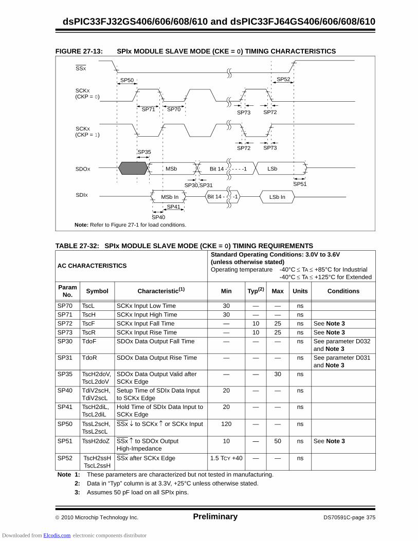
2010 Microchip Technology Inc. Preliminary DS70591C-page 375
dsPIC33FJ32GS406/606/608/610 and dsPIC33FJ64GS406/606/608/610
FIGURE 27-13: SPIx MODULE SLAVE MODE (CKE = 0) TIMING CHARACTERISTICS
SSX
SCKX(CKP = 0)
SCKX(CKP = 1)
SDOX
SP50
SP40
SP41
SP30,SP31 SP51
SP35
MSb LSbBit 14 - - - - - -1
Bit 14 - - - -1 LSb In
SP52
SP73SP72
SP72SP73SP71 SP70
Note: Refer to Figure 27-1 for load conditions.
SDIX MSb In
TABLE 27-32: SPIx MODULE SLAVE MODE (CKE = 0) TIMING REQUIREMENTS
AC CHARACTERISTICS
Standard Operating Conditions: 3.0V to 3.6V(unless otherwise stated)Operating temperature -40°C TA +85°C for Industrial
-40°C TA +125°C for Extended
ParamNo.
Symbol Characteristic(1) Min Typ(2) Max Units Conditions
SP70 TscL SCKx Input Low Time 30 — — ns
SP71 TscH SCKx Input High Time 30 — — ns
SP72 TscF SCKx Input Fall Time — 10 25 ns See Note 3
SP73 TscR SCKx Input Rise Time — 10 25 ns See Note 3
SP30 TdoF SDOx Data Output Fall Time — — — ns See parameter D032 and Note 3
SP31 TdoR SDOx Data Output Rise Time — — — ns See parameter D031 and Note 3
SP35 TscH2doV,TscL2doV
SDOx Data Output Valid after SCKx Edge
— — 30 ns
SP40 TdiV2scH, TdiV2scL
Setup Time of SDIx Data Input to SCKx Edge
20 — — ns
SP41 TscH2diL, TscL2diL
Hold Time of SDIx Data Input to SCKx Edge
20 — — ns
SP50 TssL2scH, TssL2scL
SSx to SCKx or SCKx Input 120 — — ns
SP51 TssH2doZ SSx to SDOx OutputHigh-Impedance
10 — 50 ns See Note 3
SP52 TscH2ssHTscL2ssH
SSx after SCKx Edge 1.5 TCY +40 — — ns
Note 1: These parameters are characterized but not tested in manufacturing.
2: Data in “Typ” column is at 3.3V, +25°C unless otherwise stated.
3: Assumes 50 pF load on all SPIx pins.
Downloaded from Elcodis.com electronic components distributor
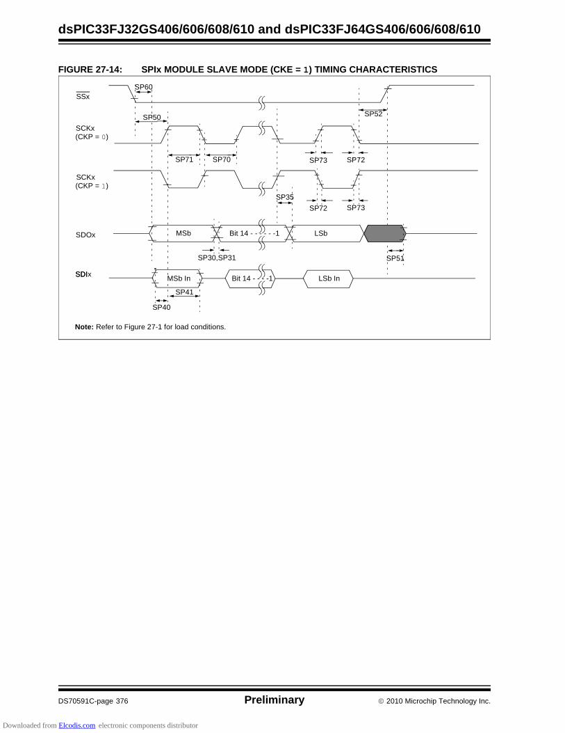
dsPIC33FJ32GS406/606/608/610 and dsPIC33FJ64GS406/606/608/610
DS70591C-page 376 Preliminary 2010 Microchip Technology Inc.
FIGURE 27-14: SPIx MODULE SLAVE MODE (CKE = 1) TIMING CHARACTERISTICS
SSx
SCKx(CKP = 0)
SCKx(CKP = 1)
SDOx
SDI
SP50
SP60
SDIx
SP30,SP31
MSb Bit 14 - - - - - -1 LSb
SP51
Bit 14 - - - -1 LSb In
SP35
SP52
SP73SP72
SP72SP73SP71 SP70
SP40
SP41
Note: Refer to Figure 27-1 for load conditions.
MSb In
Downloaded from Elcodis.com electronic components distributor

2010 Microchip Technology Inc. Preliminary DS70591C-page 377
dsPIC33FJ32GS406/606/608/610 and dsPIC33FJ64GS406/606/608/610
TABLE 27-33: SPIx MODULE SLAVE MODE (CKE = 1) TIMING REQUIREMENTS
AC CHARACTERISTICS
Standard Operating Conditions: 3.0V to 3.6V(unless otherwise stated)Operating temperature -40°C TA +85°C for Industrial
-40°C TA +125°C for Extended
ParamNo.
Symbol Characteristic(1) Min Typ(2) Max Units Conditions
SP70 TscL SCKx Input Low Time 30 — — ns
SP71 TscH SCKx Input High Time 30 — — ns
SP72 TscF SCKx Input Fall Time — 10 25 ns See Note 3
SP73 TscR SCKx Input Rise Time — 10 25 ns See Note 3
SP30 TdoF SDOx Data Output Fall Time — — — ns See parameter D032 and Note 3
SP31 TdoR SDOx Data Output Rise Time — — — ns See parameter D031 and Note 3
SP35 TscH2doV,TscL2doV
SDOx Data Output Valid afterSCKx Edge
— — 30 ns
SP40 TdiV2scH, TdiV2scL
Setup Time of SDIx Data Inputto SCKx Edge
20 — — ns
SP41 TscH2diL, TscL2diL
Hold Time of SDIx Data Inputto SCKx Edge
20 — — ns
SP50 TssL2scH, TssL2scL
SSx to SCKx or SCKx Input
120 — — ns
SP51 TssH2doZ SSx to SDOX OutputHigh-Impedance
10 — 50 ns See Note 4
SP52 TscH2ssHTscL2ssH
SSx after SCKx Edge 1.5 TCY + 40 — — ns
SP60 TssL2doV SDOx Data Output Valid afterSSx Edge
— — 50 ns
Note 1: These parameters are characterized but not tested in manufacturing.
2: Data in “Typ” column is at 3.3V, +25°C unless otherwise stated.
3: The minimum clock period for SCKx is 100 ns. The clock generated in Master mode must not violate this specification.
4: Assumes 50 pF load on all SPIx pins.
Downloaded from Elcodis.com electronic components distributor

dsPIC33FJ32GS406/606/608/610 and dsPIC33FJ64GS406/606/608/610
DS70591C-page 378 Preliminary 2010 Microchip Technology Inc.
FIGURE 27-15: I2Cx BUS START/STOP BITS TIMING CHARACTERISTICS (MASTER MODE)
FIGURE 27-16: I2Cx BUS DATA TIMING CHARACTERISTICS (MASTER MODE)
IM31 IM34
SCLx
SDAx
StartCondition
StopCondition
IM30 IM33
Note: Refer to Figure 27-1 for load conditions.
IM11IM10 IM33
IM11
IM10
IM20
IM26IM25
IM40 IM40 IM45
IM21
SCLx
SDAxIn
SDAxOut
Note: Refer to Figure 27-1 for load conditions.
Downloaded from Elcodis.com electronic components distributor

2010 Microchip Technology Inc. Preliminary DS70591C-page 379
dsPIC33FJ32GS406/606/608/610 and dsPIC33FJ64GS406/606/608/610
TABLE 27-34: I2Cx BUS DATA TIMING REQUIREMENTS (MASTER MODE)
AC CHARACTERISTICS
Standard Operating Conditions: 3.0V to 3.6V(unless otherwise stated)Operating temperature -40°C TA +85°C for Industrial
-40°C TA +125°C for Extended
ParamNo.
Symbol Characteristic Min(1) Max Units Conditions
IM10 TLO:SCL Clock Low Time 100 kHz mode TCY/2 (BRG + 1) — s
400 kHz mode TCY/2 (BRG + 1) — s
1 MHz mode(2) TCY/2 (BRG + 1) — s
IM11 THI:SCL Clock High Time 100 kHz mode TCY/2 (BRG + 1) — s
400 kHz mode TCY/2 (BRG + 1) — s
1 MHz mode(2) TCY/2 (BRG + 1) — s
IM20 TF:SCL SDAx and SCLxFall Time
100 kHz mode — 300 ns CB is specified to be from 10 to 400 pF400 kHz mode 20 + 0.1 CB 300 ns
1 MHz mode(2) — 100 ns
IM21 TR:SCL SDAx and SCLxRise Time
100 kHz mode — 1000 ns CB is specified to be from 10 to 400 pF400 kHz mode 20 + 0.1 CB 300 ns
1 MHz mode(2) — 300 ns
IM25 TSU:DAT Data InputSetup Time
100 kHz mode 250 — ns
400 kHz mode 100 — ns
1 MHz mode(2) 40 — ns
IM26 THD:DAT Data InputHold Time
100 kHz mode 0 — s
400 kHz mode 0 0.9 s
1 MHz mode(2) 0.2 — s
IM30 TSU:STA Start ConditionSetup Time
100 kHz mode TCY/2 (BRG + 1) — s Only relevant for Repeated Startcondition
400 kHz mode TCY/2 (BRG + 1) — s
1 MHz mode(2) TCY/2 (BRG + 1) — s
IM31 THD:STA Start Condition Hold Time
100 kHz mode TCY/2 (BRG + 1) — s After this period thefirst clock pulse isgenerated
400 kHz mode TCY/2 (BRG + 1) — s
1 MHz mode(2) TCY/2 (BRG + 1) — s
IM33 TSU:STO Stop Condition Setup Time
100 kHz mode TCY/2 (BRG + 1) — s
400 kHz mode TCY/2 (BRG + 1) — s
1 MHz mode(2) TCY/2 (BRG + 1) — s
IM34 THD:STO Stop Condition 100 kHz mode TCY/2 (BRG + 1) — ns
Hold Time 400 kHz mode TCY/2 (BRG + 1) — ns
1 MHz mode(2) TCY/2 (BRG + 1) — ns
IM40 TAA:SCL Output Valid From Clock
100 kHz mode — 3500 ns
400 kHz mode — 1000 ns
1 MHz mode(2) — 400 ns
IM45 TBF:SDA Bus Free Time 100 kHz mode 4.7 — s Time the bus must be free before a newtransmission can start
400 kHz mode 1.3 — s
1 MHz mode(2) 0.5 — s
IM50 CB Bus Capacitive Loading — 400 pF
IM51 TPGD Pulse Gobbler Delay 65 390 ns See Note 3
Note 1: BRG is the value of the I2C™ Baud Rate Generator. Refer to Section 19. “Inter-Integrated Circuit (I2C™)” (DS70195) in the “dsPIC33F/PIC24F Family Reference Manual”.
2: Maximum pin capacitance = 10 pF for all I2Cx pins (for 1 MHz mode only).
3: Typical value for this parameter is 130 ns.
Downloaded from Elcodis.com electronic components distributor

dsPIC33FJ32GS406/606/608/610 and dsPIC33FJ64GS406/606/608/610
DS70591C-page 380 Preliminary 2010 Microchip Technology Inc.
FIGURE 27-17: I2Cx BUS START/STOP BITS TIMING CHARACTERISTICS (SLAVE MODE)
FIGURE 27-18: I2Cx BUS DATA TIMING CHARACTERISTICS (SLAVE MODE)
IS31 IS34SCLx
SDAx
StartCondition
StopCondition
IS30 IS33
IS30IS31 IS33
IS11
IS10
IS20
IS26IS25
IS40 IS40 IS45
IS21
SCLx
SDAxIn
SDAxOut
Downloaded from Elcodis.com electronic components distributor
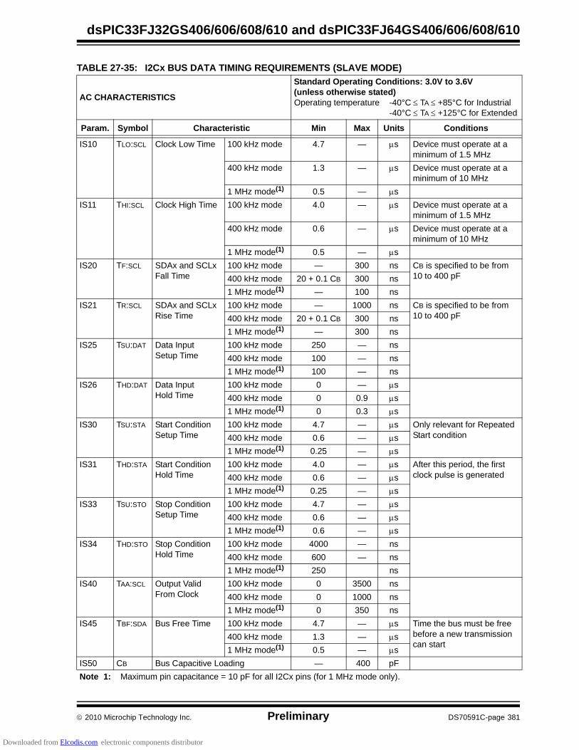
2010 Microchip Technology Inc. Preliminary DS70591C-page 381
dsPIC33FJ32GS406/606/608/610 and dsPIC33FJ64GS406/606/608/610
TABLE 27-35: I2Cx BUS DATA TIMING REQUIREMENTS (SLAVE MODE)
AC CHARACTERISTICS
Standard Operating Conditions: 3.0V to 3.6V(unless otherwise stated)Operating temperature -40°C TA +85°C for Industrial
-40°C TA +125°C for Extended
Param. Symbol Characteristic Min Max Units Conditions
IS10 TLO:SCL Clock Low Time 100 kHz mode 4.7 — s Device must operate at a minimum of 1.5 MHz
400 kHz mode 1.3 — s Device must operate at a minimum of 10 MHz
1 MHz mode(1) 0.5 — s
IS11 THI:SCL Clock High Time 100 kHz mode 4.0 — s Device must operate at a minimum of 1.5 MHz
400 kHz mode 0.6 — s Device must operate at a minimum of 10 MHz
1 MHz mode(1) 0.5 — s
IS20 TF:SCL SDAx and SCLxFall Time
100 kHz mode — 300 ns CB is specified to be from10 to 400 pF400 kHz mode 20 + 0.1 CB 300 ns
1 MHz mode(1) — 100 ns
IS21 TR:SCL SDAx and SCLxRise Time
100 kHz mode — 1000 ns CB is specified to be from10 to 400 pF400 kHz mode 20 + 0.1 CB 300 ns
1 MHz mode(1) — 300 ns
IS25 TSU:DAT Data InputSetup Time
100 kHz mode 250 — ns
400 kHz mode 100 — ns
1 MHz mode(1) 100 — ns
IS26 THD:DAT Data InputHold Time
100 kHz mode 0 — s
400 kHz mode 0 0.9 s
1 MHz mode(1) 0 0.3 s
IS30 TSU:STA Start ConditionSetup Time
100 kHz mode 4.7 — s Only relevant for Repeated Start condition400 kHz mode 0.6 — s
1 MHz mode(1) 0.25 — s
IS31 THD:STA Start Condition Hold Time
100 kHz mode 4.0 — s After this period, the first clock pulse is generated400 kHz mode 0.6 — s
1 MHz mode(1) 0.25 — s
IS33 TSU:STO Stop Condition Setup Time
100 kHz mode 4.7 — s
400 kHz mode 0.6 — s
1 MHz mode(1) 0.6 — s
IS34 THD:STO Stop ConditionHold Time
100 kHz mode 4000 — ns
400 kHz mode 600 — ns
1 MHz mode(1) 250 ns
IS40 TAA:SCL Output Valid From Clock
100 kHz mode 0 3500 ns
400 kHz mode 0 1000 ns
1 MHz mode(1) 0 350 ns
IS45 TBF:SDA Bus Free Time 100 kHz mode 4.7 — s Time the bus must be free before a new transmission can start
400 kHz mode 1.3 — s
1 MHz mode(1) 0.5 — s
IS50 CB Bus Capacitive Loading — 400 pF
Note 1: Maximum pin capacitance = 10 pF for all I2Cx pins (for 1 MHz mode only).
Downloaded from Elcodis.com electronic components distributor
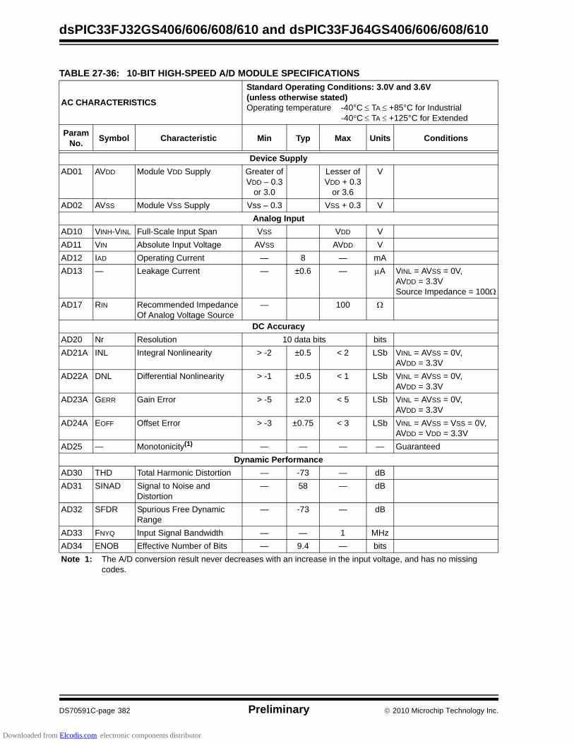
dsPIC33FJ32GS406/606/608/610 and dsPIC33FJ64GS406/606/608/610
DS70591C-page 382 Preliminary 2010 Microchip Technology Inc.
TABLE 27-36: 10-BIT HIGH-SPEED A/D MODULE SPECIFICATIONS
AC CHARACTERISTICS
Standard Operating Conditions: 3.0V and 3.6V(unless otherwise stated)Operating temperature -40°C TA +85°C for Industrial
-40°C TA +125°C for Extended
Param No.
Symbol Characteristic Min Typ Max Units Conditions
Device Supply
AD01 AVDD Module VDD Supply Greater ofVDD – 0.3
or 3.0
Lesser ofVDD + 0.3
or 3.6
V
AD02 AVSS Module VSS Supply Vss – 0.3 VSS + 0.3 V
Analog Input
AD10 VINH-VINL Full-Scale Input Span VSS VDD V
AD11 VIN Absolute Input Voltage AVSS AVDD V
AD12 IAD Operating Current — 8 — mA
AD13 — Leakage Current — ±0.6 — A VINL = AVSS = 0V,AVDD = 3.3VSource Impedance = 100
AD17 RIN Recommended ImpedanceOf Analog Voltage Source
— 100
DC Accuracy
AD20 Nr Resolution 10 data bits bits
AD21A INL Integral Nonlinearity > -2 ±0.5 < 2 LSb VINL = AVSS = 0V,AVDD = 3.3V
AD22A DNL Differential Nonlinearity > -1 ±0.5 < 1 LSb VINL = AVSS = 0V,AVDD = 3.3V
AD23A GERR Gain Error > -5 ±2.0 < 5 LSb VINL = AVSS = 0V,AVDD = 3.3V
AD24A EOFF Offset Error > -3 ±0.75 < 3 LSb VINL = AVSS = VSS = 0V, AVDD = VDD = 3.3V
AD25 — Monotonicity(1) — — — — Guaranteed
Dynamic Performance
AD30 THD Total Harmonic Distortion — -73 — dB
AD31 SINAD Signal to Noise andDistortion
— 58 — dB
AD32 SFDR Spurious Free Dynamic Range
— -73 — dB
AD33 FNYQ Input Signal Bandwidth — — 1 MHz
AD34 ENOB Effective Number of Bits — 9.4 — bits
Note 1: The A/D conversion result never decreases with an increase in the input voltage, and has no missing codes.
Downloaded from Elcodis.com electronic components distributor

2010 Microchip Technology Inc. Preliminary DS70591C-page 383
dsPIC33FJ32GS406/606/608/610 and dsPIC33FJ64GS406/606/608/610
FIGURE 27-19: A/D CONVERSION TIMING PER INPUT
TABLE 27-37: 10-BIT HIGH-SPEED A/D MODULE TIMING REQUIREMENTS
AC CHARACTERISTICS
Standard Operating Conditions: 3.0V to 3.6V(unless otherwise stated)Operating temperature -40°C TA +85°C for Industrial
-40°C TA +125°C for Extended
Param No.
Symbol Characteristic Min Typ(1) Max Units Conditions
Clock Parameters
AD50b TAD ADC Clock Period 35.8 — — ns
Conversion Rate
AD55b tCONV Conversion Time — 14 TAD — —
AD56b FCNV Throughput Rate
Devices with Single SAR — — 2.0 Msps
Devices with Dual SARs — — 4.0 Msps
Timing Parameters
AD63b tDPU Time to Stabilize Analog Stage from ADC Off to ADC On(1)
1.0 — 10 s
Note 1: These parameters are characterized but not tested in manufacturing.
TAD
A/D Data
ADBUFxx
9 8 2 1 0
Old Data New Data
CONV
A/D Clock
Trigger Pulse
Tconv
Downloaded from Elcodis.com electronic components distributor
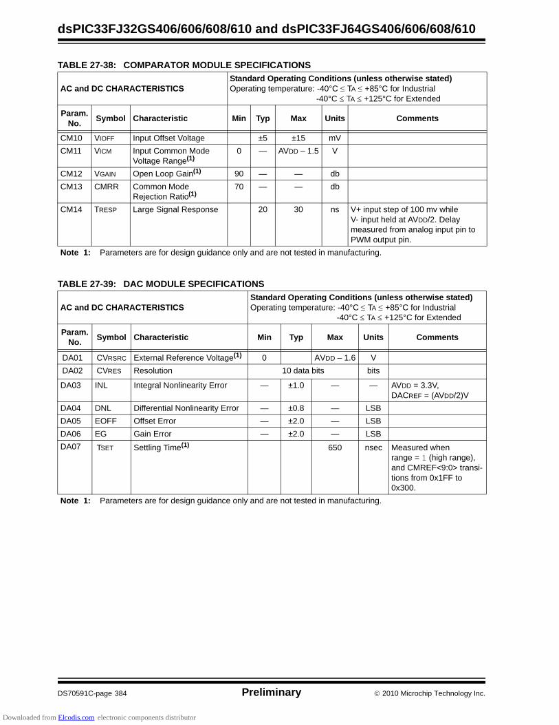
dsPIC33FJ32GS406/606/608/610 and dsPIC33FJ64GS406/606/608/610
DS70591C-page 384 Preliminary 2010 Microchip Technology Inc.
TABLE 27-38: COMPARATOR MODULE SPECIFICATIONS
AC and DC CHARACTERISTICSStandard Operating Conditions (unless otherwise stated)
Operating temperature: -40°C TA +85°C for Industrial-40°C TA +125°C for Extended
Param. No.
Symbol Characteristic Min Typ Max Units Comments
CM10 VIOFF Input Offset Voltage ±5 ±15 mV
CM11 VICM Input Common Mode Voltage Range(1)
0 — AVDD – 1.5 V
CM12 VGAIN Open Loop Gain(1) 90 — — db
CM13 CMRR Common Mode Rejection Ratio(1)
70 — — db
CM14 TRESP Large Signal Response 20 30 ns V+ input step of 100 mv while V- input held at AVDD/2. Delay measured from analog input pin to PWM output pin.
Note 1: Parameters are for design guidance only and are not tested in manufacturing.
TABLE 27-39: DAC MODULE SPECIFICATIONS
AC and DC CHARACTERISTICS Standard Operating Conditions (unless otherwise stated) Operating temperature: -40°C TA +85°C for Industrial
-40°C TA +125°C for Extended
Param. No.
Symbol Characteristic Min Typ Max Units Comments
DA01 CVRSRC External Reference Voltage(1) 0 AVDD – 1.6 V
DA02 CVRES Resolution 10 data bits bits
DA03 INL Integral Nonlinearity Error — ±1.0 — — AVDD = 3.3V, DACREF = (AVDD/2)V
DA04 DNL Differential Nonlinearity Error — ±0.8 — LSB
DA05 EOFF Offset Error — ±2.0 — LSB
DA06 EG Gain Error — ±2.0 — LSB
DA07 TSET Settling Time(1) 650 nsec Measured when range = 1 (high range), and CMREF<9:0> transi-tions from 0x1FF to 0x300.
Note 1: Parameters are for design guidance only and are not tested in manufacturing.
Downloaded from Elcodis.com electronic components distributor
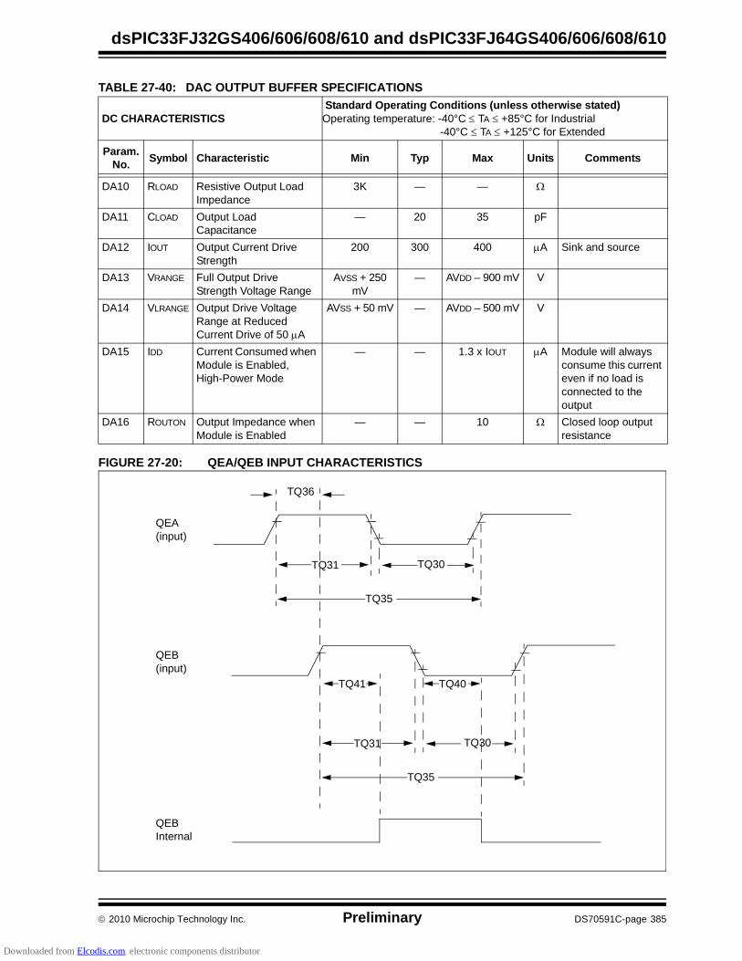
2010 Microchip Technology Inc. Preliminary DS70591C-page 385
dsPIC33FJ32GS406/606/608/610 and dsPIC33FJ64GS406/606/608/610
FIGURE 27-20: QEA/QEB INPUT CHARACTERISTICS
TABLE 27-40: DAC OUTPUT BUFFER SPECIFICATIONS
DC CHARACTERISTICSStandard Operating Conditions (unless otherwise stated)
Operating temperature: -40°C TA +85°C for Industrial-40°C TA +125°C for Extended
Param. No.
Symbol Characteristic Min Typ Max Units Comments
DA10 RLOAD Resistive Output Load Impedance
3K — —
DA11 CLOAD Output Load Capacitance
— 20 35 pF
DA12 IOUT Output Current Drive Strength
200 300 400 A Sink and source
DA13 VRANGE Full Output Drive Strength Voltage Range
AVSS + 250 mV
— AVDD – 900 mV V
DA14 VLRANGE Output Drive Voltage Range at Reduced Current Drive of 50 A
AVSS + 50 mV — AVDD – 500 mV V
DA15 IDD Current Consumed when Module is Enabled, High-Power Mode
— — 1.3 x IOUT A Module will always consume this current even if no load is connected to the output
DA16 ROUTON Output Impedance when Module is Enabled
— — 10 Closed loop output resistance
TQ30
TQ35
TQ31
QEA (input)
TQ30
TQ35
TQ31
QEB (input)
TQ36
QEB Internal
TQ40TQ41
Downloaded from Elcodis.com electronic components distributor

dsPIC33FJ32GS406/606/608/610 and dsPIC33FJ64GS406/606/608/610
DS70591C-page 386 Preliminary 2010 Microchip Technology Inc.
FIGURE 27-21: QEI MODULE INDEX PULSE TIMING CHARACTERISTICS
TABLE 27-41: QUADRATURE DECODER TIMING REQUIREMENTS
AC CHARACTERISTICS
Standard Operating Conditions: 3.0V to 3.6V(unless otherwise stated)Operating temperature -40°C TA +85°C for Industrial
-40°C TA +125°C for Extended
ParamNo.
Symbol Characteristic(1) Typ(2) Max Units Conditions
TQ30 TQUL Quadrature Input Low Time 6 TCY — ns —
TQ31 TQUH Quadrature Input High Time 6 TCY — ns —
TQ35 TQUIN Quadrature Input Period 12 TCY — ns —
TQ36 TQUP Quadrature Phase Period 3 TCY — ns —
TQ40 TQUFL Filter Time to Recognize Low,with Digital Filter
3 * N * TCY — ns N = 1, 2, 4, 16, 32, 64, 128 and 256 (Note 3)
TQ41 TQUFH Filter Time to Recognize High,with Digital Filter
3 * N * TCY — ns N = 1, 2, 4, 16, 32, 64, 128 and 256 (Note 3)
Note 1: These parameters are characterized but not tested in manufacturing.
2: Data in “Typ” column is at 3.3V, 25°C unless otherwise stated.
3: N = Index Channel Digital Filter Clock Divide Select bits. Refer to Section 15. “Quadrature Encoder Interface (QEI)” in the “dsPIC33F/PIC24H Family Reference Manual”.
QEA(input)
UngatedIndex
QEB(input)
TQ55
Index Internal
Position CounterReset
TQ50TQ51
Downloaded from Elcodis.com electronic components distributor

2010 Microchip Technology Inc. Preliminary DS70591C-page 387
dsPIC33FJ32GS406/606/608/610 and dsPIC33FJ64GS406/606/608/610
FIGURE 27-22: TIMERQ (QEI MODULE) EXTERNAL CLOCK TIMING CHARACTERISTICS
TABLE 27-42: QEI INDEX PULSE TIMING REQUIREMENTS
AC CHARACTERISTICS
Standard Operating Conditions: 3.0V to 3.6V(unless otherwise stated)Operating temperature -40°C TA +85°C for Industrial
-40°C TA +125°C for Extended
ParamNo.
Symbol Characteristic(1) Min Max Units Conditions
TQ50 TqIL Filter Time to Recognize Low,with Digital Filter
3 * N * TCY — ns N = 1, 2, 4, 16, 32, 64,128 and 256 (Note 2)
TQ51 TqiH Filter Time to Recognize High,with Digital Filter
3 * N * TCY — ns N = 1, 2, 4, 16, 32, 64,128 and 256 (Note 2)
TQ55 Tqidxr Index Pulse Recognized to PositionCounter Reset (ungated index)
3 TCY — ns —
Note 1: These parameters are characterized but not tested in manufacturing.
2: Alignment of index pulses to QEA and QEB is shown for position counter Reset timing only. Shown for forward direction only (QEA leads QEB). Same timing applies for reverse direction (QEA lags QEB) but index pulse recognition occurs on falling edge.
TQ11
TQ15
TQ10
TQ20
QEB
POSCNT
TABLE 27-43: QEI MODULE EXTERNAL CLOCK TIMING REQUIREMENTS
AC CHARACTERISTICS
Standard Operating Conditions: 3.0V to 3.6V(unless otherwise stated)Operating temperature -40°C TA +85°C for Industrial
-40°C TA +125°C for Extended
ParamNo.
Symbol Characteristic(1) Min Typ Max Units Conditions
TQ10 TtQH TQCK High Time Synchronous,with prescaler
TCY + 20 — — ns Must also meet parameter TQ15
TQ11 TtQL TQCK Low Time Synchronous,with prescaler
TCY + 20 — — ns Must also meet parameter TQ15
TQ15 TtQP TQCP Input Period
Synchronous,with prescaler
2 * TCY + 40 — — ns —
TQ20 TCKEXTMRL Delay from External TxCK Clock Edge to Timer Increment
0.5 TCY — 1.5 TCY — —
Note 1: These parameters are characterized but not tested in manufacturing.
Downloaded from Elcodis.com electronic components distributor
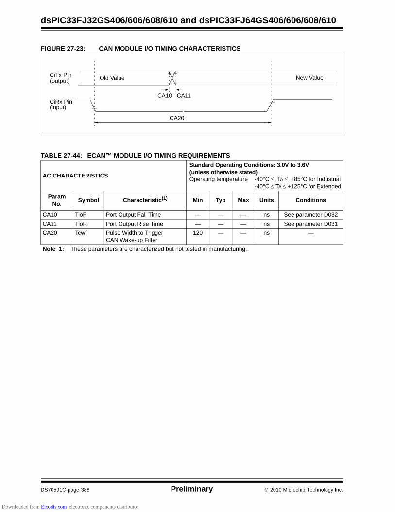
dsPIC33FJ32GS406/606/608/610 and dsPIC33FJ64GS406/606/608/610
DS70591C-page 388 Preliminary 2010 Microchip Technology Inc.
FIGURE 27-23: CAN MODULE I/O TIMING CHARACTERISTICS
CiTx Pin(output)
CA10 CA11
Old Value New Value
CA20
CiRx Pin(input)
TABLE 27-44: ECAN™ MODULE I/O TIMING REQUIREMENTS
AC CHARACTERISTICS
Standard Operating Conditions: 3.0V to 3.6V(unless otherwise stated)Operating temperature -40°C TA +85°C for Industrial
-40°C TA +125°C for Extended
ParamNo.
Symbol Characteristic(1) Min Typ Max Units Conditions
CA10 TioF Port Output Fall Time — — — ns See parameter D032
CA11 TioR Port Output Rise Time — — — ns See parameter D031
CA20 Tcwf Pulse Width to TriggerCAN Wake-up Filter
120 — — ns —
Note 1: These parameters are characterized but not tested in manufacturing.
Downloaded from Elcodis.com electronic components distributor
2010 Microchip Technology Inc. Preliminary DS70591C-page 389
dsPIC33FJ32GS406/606/608/610 and dsPIC33FJ64GS406/606/608/610
28.0 PACKAGING INFORMATION
Legend: XX...X Customer-specific informationY Year code (last digit of calendar year)YY Year code (last 2 digits of calendar year)WW Week code (week of January 1 is week ‘01’)NNN Alphanumeric traceability code Pb-free JEDEC designator for Matte Tin (Sn)* This package is Pb-free. The Pb-free JEDEC designator ( )
can be found on the outer packaging for this package.
Note: If the full Microchip part number cannot be marked on one line, it is carried over to the nextline, thus limiting the number of available characters for customer-specific information.
3e
3e
64-Lead TQFP (10x10x1mm)
XXXXXXXXXXXXXXXXXXXXXXXXXXXXXX
YYWWNNN
Example
dsPIC33FJ32GS406
0610017
80-Lead TQFP (12x12x1mm)
XXXXXXXXXXXXXXXXXXXXXXXX
YYWWNNN
Example
33FJ32GS608-I/PT
0610017
-I/PT 3e
3e
64-Lead QFN (9x9x0.9mm) Example
XXXXXXXXXXXXXXXXXXXX
YYWWNNN
33FJ32FJ32GS406-I/MR
0610017
3e
Downloaded from Elcodis.com electronic components distributor
dsPIC33FJ32GS406/606/608/610 and dsPIC33FJ64GS406/606/608/610
DS70591C-page 390 Preliminary 2010 Microchip Technology Inc.
Legend: XX...X Customer-specific informationY Year code (last digit of calendar year)YY Year code (last 2 digits of calendar year)WW Week code (week of January 1 is week ‘01’)NNN Alphanumeric traceability code Pb-free JEDEC designator for Matte Tin (Sn)* This package is Pb-free. The Pb-free JEDEC designator ( )
can be found on the outer packaging for this package.
Note: If the full Microchip part number cannot be marked on one line, it is carried over to the nextline, thus limiting the number of available characters for customer-specific information.
3e
3e
100-Lead TQFP (14x14x1mm)
XXXXXXXXXXXXXXXXXXXXXXXX
YYWWNNN
Example
33FJ32GS610-I/PF
06100173e
100-Lead TQFP (12x12x1 mm)
XXXXXXXXXXXXXXXXXXXXXXXX
YYWWNNN
Example
dsPIC33FJ64GS608-I/PT
05100173e
Downloaded from Elcodis.com electronic components distributor
2010 Microchip Technology Inc. Preliminary DS70591C-page 391
dsPIC33FJ32GS406/606/608/610 and dsPIC33FJ64GS406/606/608/610
28.1 Package Details
Note: For the most current package drawings, please see the Microchip Packaging Specification located at http://www.microchip.com/packaging
Downloaded from Elcodis.com electronic components distributor

dsPIC33FJ32GS406/606/608/610 and dsPIC33FJ64GS406/606/608/610
DS70591C-page 392 Preliminary 2010 Microchip Technology Inc.
Note: For the most current package drawings, please see the Microchip Packaging Specification located at http://www.microchip.com/packaging
Downloaded from Elcodis.com electronic components distributor

2010 Microchip Technology Inc. Preliminary DS70591C-page 393
dsPIC33FJ32GS406/606/608/610 and dsPIC33FJ64GS406/606/608/610
Note: For the most current package drawings, please see the Microchip Packaging Specification located at http://www.microchip.com/packaging
Downloaded from Elcodis.com electronic components distributor
dsPIC33FJ32GS406/606/608/610 and dsPIC33FJ64GS406/606/608/610
DS70591C-page 394 Preliminary 2010 Microchip Technology Inc.
���������� ������������� ������������������ �!"#$����%���&
' ��(�� ������ �!"�����# $�% �&"� �'��� ���(�)"&�'"!&�) �����& #�*�&����&� ���&�� #��� ���� +��'% �!��&����� �!��� ��&�����,�!�- �'��� ������ ��' �!���!������#�.��#����&�����"# �'��#�%��!�������&�"!���!�����#�%��!�������&�"!���!�!�������&� $� #����/�''� ��!�# ��� ��' �!���������#�&�� �������� �����.�0���/��
1�+2 1�!�����' �!������� �� &������� $��&� ��" �!��*��*�&��"&�&�� ���� !��.32 � % � �� ���' �!���(�"!"�����*�&��"&�&�� ���� (�%�����%��'�&����"��! !������
' �( 3���&� �'�!&��"�� �&���4�� �#��*���!(�� �! �! �&� �������������4������� ��%���&��������& #��&��&&255***�'����������'5��4�����
6��&! ��77��.�.����' �!����7�'�&! ��8 89� ��:
8"') ���%�7 �#! 8 ;�7 �#���&�� ��/��1�+9 �����< ���& � = = �������# #����4�� �����4� !! �� ���/ ���� ���/�&��#�%%�� �� ���/ = ���/3��&�7 ��&� 7 ���/ ��;� ���/3��&���& 7� ������.33��&����� � �> ��/> �>9 �����?�#&� . ������1�+9 �����7 ��&� � ������1�+���# #����4�� �?�#&� .� ������1�+���# #����4�� �7 ��&� �� ������1�+7 �#�����4� !! � ���� = ����7 �#�?�#&� ) ���� ���� �������#����%&����� ��� � ��> ��> ��>���#����%&����� �1�&&�' � ��> ��> ��>
D
D1
E
E1
e
b
N
NOTE 1 1 2 3 NOTE 2
c
LA1
L1
A2
Aφ
β
α
�������� � �������� ���*��� +���@/1
Downloaded from Elcodis.com electronic components distributor

2010 Microchip Technology Inc. Preliminary DS70591C-page 395
dsPIC33FJ32GS406/606/608/610 and dsPIC33FJ64GS406/606/608/610
���������� ������������� ������������������ �!"#$����%���&
' �( 3���&� �'�!&��"�� �&���4�� �#��*���!(�� �! �! �&� �������������4������� ��%���&��������& #��&��&&255***�'����������'5��4�����
Downloaded from Elcodis.com electronic components distributor

dsPIC33FJ32GS406/606/608/610 and dsPIC33FJ64GS406/606/608/610
DS70591C-page 396 Preliminary 2010 Microchip Technology Inc.
)��������� ������������� ���������#��#����� �!"#$����%���&
' ��(�� ������ �!"�����# $�% �&"� �'��� ���(�)"&�'"!&�) �����& #�*�&����&� ���&�� #��� ���� +��'% �!��&����� �!��� ��&�����,�!�- �'��� ������ ��' �!���!������#�.��#����&�����"# �'��#�%��!�������&�"!���!�����#�%��!�������&�"!���!�!�������&� $� #����/�''� ��!�# ��� ��' �!���������#�&�� �������� �����.�0���/��
1�+2 1�!�����' �!������� �� &������� $��&� ��" �!��*��*�&��"&�&�� ���� !��.32 � % � �� ���' �!���(�"!"�����*�&��"&�&�� ���� (�%�����%��'�&����"��! !������
' �( 3���&� �'�!&��"�� �&���4�� �#��*���!(�� �! �! �&� �������������4������� ��%���&��������& #��&��&&255***�'����������'5��4�����
6��&! ��77��.�.����' �!����7�'�&! ��8 89� ��:
8"') ���%�7 �#! 8 @�7 �#���&�� ��/��1�+9 �����< ���& � = = �������# #����4�� �����4� !! �� ���/ ���� ���/�&��#�%%�� �� ���/ = ���/3��&�7 ��&� 7 ���/ ��;� ���/3��&���& 7� ������.33��&����� � �> ��/> �>9 �����?�#&� . ������1�+9 �����7 ��&� � ������1�+���# #����4�� �?�#&� .� ������1�+���# #����4�� �7 ��&� �� ������1�+7 �#�����4� !! � ���� = ����7 �#�?�#&� ) ���� ���� �������#����%&����� ��� � ��> ��> ��>���#����%&����� �1�&&�' � ��> ��> ��>
D
D1
E
E1e
b N
NOTE 112 3 NOTE 2
A
A2L1
A1L
c
α
βφ
�������� � �������� ���*��� +�����1
Downloaded from Elcodis.com electronic components distributor

2010 Microchip Technology Inc. Preliminary DS70591C-page 397
dsPIC33FJ32GS406/606/608/610 and dsPIC33FJ64GS406/606/608/610
)��������� ������������� ���������#��#����� �!"#$����%���&
' �( 3���&� �'�!&��"�� �&���4�� �#��*���!(�� �! �! �&� �������������4������� ��%���&��������& #��&��&&255***�'����������'5��4�����
Downloaded from Elcodis.com electronic components distributor
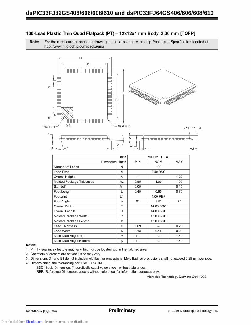
dsPIC33FJ32GS406/606/608/610 and dsPIC33FJ64GS406/606/608/610
DS70591C-page 398 Preliminary 2010 Microchip Technology Inc.
����������� ������������� ���������#��#����� �!"#$����%���&
' ��(�� ������ �!"�����# $�% �&"� �'��� ���(�)"&�'"!&�) �����& #�*�&����&� ���&�� #��� ���� +��'% �!��&����� �!��� ��&�����,�!�- �'��� ������ ��' �!���!������#�.��#����&�����"# �'��#�%��!�������&�"!���!�����#�%��!�������&�"!���!�!�������&� $� #����/�''� ��!�# ��� ��' �!���������#�&�� �������� �����.�0���/��
1�+2 1�!�����' �!������� �� &������� $��&� ��" �!��*��*�&��"&�&�� ���� !��.32 � % � �� ���' �!���(�"!"�����*�&��"&�&�� ���� (�%�����%��'�&����"��! !������
' �( 3���&� �'�!&��"�� �&���4�� �#��*���!(�� �! �! �&� �������������4������� ��%���&��������& #��&��&&255***�'����������'5��4�����
6��&! ��77��.�.����' �!����7�'�&! ��8 89� ��:
8"') ���%�7 �#! 8 ���7 �#���&�� �����1�+9 �����< ���& � = = �������# #����4�� �����4� !! �� ���/ ���� ���/�&��#�%%�� �� ���/ = ���/3��&�7 ��&� 7 ���/ ��;� ���/3��&���& 7� ������.33��&����� � �> ��/> �>9 �����?�#&� . ������1�+9 �����7 ��&� � ������1�+���# #����4�� �?�#&� .� ������1�+���# #����4�� �7 ��&� �� ������1�+7 �#�����4� !! � ���� = ����7 �#�?�#&� ) ���� ���@ �������#����%&����� ��� � ��> ��> ��>���#����%&����� �1�&&�' � ��> ��> ��>
D
D1
E
E1
e
bN
123NOTE 1 NOTE 2
c
LA1
L1
A
A2
α
βφ
�������� � �������� ���*��� +�����1
Downloaded from Elcodis.com electronic components distributor

2010 Microchip Technology Inc. Preliminary DS70591C-page 399
dsPIC33FJ32GS406/606/608/610 and dsPIC33FJ64GS406/606/608/610
����������� ������������� ���������#��#����� �!"#$����%���&
' �( 3���&� �'�!&��"�� �&���4�� �#��*���!(�� �! �! �&� �������������4������� ��%���&��������& #��&��&&255***�'����������'5��4�����
Downloaded from Elcodis.com electronic components distributor

dsPIC33FJ32GS406/606/608/610 and dsPIC33FJ64GS406/606/608/610
DS70591C-page 400 Preliminary 2010 Microchip Technology Inc.
����������� ������������� ������������������ �!"#$����%���&
' ��(�� ������ �!"�����# $�% �&"� �'��� ���(�)"&�'"!&�) �����& #�*�&����&� ���&�� #��� ���� +��'% �!��&����� �!��� ��&�����,�!�- �'��� ������ ��' �!���!������#�.��#����&�����"# �'��#�%��!�������&�"!���!�����#�%��!�������&�"!���!�!�������&� $� #����/�''� ��!�# ��� ��' �!���������#�&�� �������� �����.�0���/��
1�+2 1�!�����' �!������� �� &������� $��&� ��" �!��*��*�&��"&�&�� ���� !��.32 � % � �� ���' �!���(�"!"�����*�&��"&�&�� ���� (�%�����%��'�&����"��! !������
' �( 3���&� �'�!&��"�� �&���4�� �#��*���!(�� �! �! �&� �������������4������� ��%���&��������& #��&��&&255***�'����������'5��4�����
6��&! ��77��.�.����' �!����7�'�&! ��8 89� ��:
8"') ���%�7 �#! 8 ���7 �#���&�� ��/��1�+9 �����< ���& � = = �������# #����4�� �����4� !! �� ���/ ���� ���/�&��#�%%�� �� ���/ = ���/3��&�7 ��&� 7 ���/ ��;� ���/3��&���& 7� ������.33��&����� � �> ��/> �>9 �����?�#&� . �;����1�+9 �����7 ��&� � �;����1�+���# #����4�� �?�#&� .� ������1�+���# #����4�� �7 ��&� �� ������1�+7 �#�����4� !! � ���� = ����7 �#�?�#&� ) ���� ���� �������#����%&����� ��� � ��> ��> ��>���#����%&����� �1�&&�' � ��> ��> ��>
D
D1
e
b
E1
E
N
NOTE 1 NOTE 21 23
c
LA1 L1
A2
A
φβ
α
�������� � �������� ���*��� +�����1
Downloaded from Elcodis.com electronic components distributor

2010 Microchip Technology Inc. Preliminary DS70591C-page 401
dsPIC33FJ32GS406/606/608/610 and dsPIC33FJ64GS406/606/608/610
����������� ������������� ������������������ �!"#$����%���&
' �( 3���&� �'�!&��"�� �&���4�� �#��*���!(�� �! �! �&� �������������4������� ��%���&��������& #��&��&&255***�'����������'5��4�����
Downloaded from Elcodis.com electronic components distributor

dsPIC33FJ32GS406/606/608/610 and dsPIC33FJ64GS406/606/608/610
DS70591C-page 402 Preliminary 2010 Microchip Technology Inc.
NOTES:
Downloaded from Elcodis.com electronic components distributor
2010 Microchip Technology Inc. Preliminary DS70591C-page 403
dsPIC33FJ32GS406/606/608/610 and dsPIC33FJ64GS406/606/608/610
APPENDIX A: MIGRATING FROM dsPIC33FJ06GS101/X02 AND dsPIC33FJ16GSX02/X04 TO dsPIC33FJ32GS406/606/608/610 AND dsPIC33FJ64GS406/606/608/610 DEVICES
This appendix provides an overview of considerationsfor migrating from the dsPIC33FJ06GS101/X02 anddsPIC33FJ16GSX02/X04 family of devices to thedsPIC33FJ32GS406/606/608/610 anddsPIC33FJ64GS406/606/608/610 family of devices.The code developed for the dsPIC33FJ06GS101/X02and dsPIC33FJ16GSX02/X04 devices can be portedto the dsPIC33FJ32GS406/606/608/610 anddsPIC33FJ64GS406/606/608/610 devices aftermaking the appropriate changes outlined below.
A.1 Device Pins and Peripheral Pin Select (PPS)
On dsPIC33FJ06GS101/X02 anddsPIC33FJ16GSX02/X04 devices, some peripheralssuch as the Timer, Input Capture, Output Compare,UART, SPI, External Interrupts, Analog ComparatorOutput, as well as the PWM4 pin pair, were mapped tophysical pins via Peripheral Pin Select (PPS)functionality. On dsPIC33FJ32GS406/606/608/610and dsPIC33FJ64GS406/606/608/610 devices, theseperipherals are hard-coded to dedicated pins. Becauseof this, as well as pinout differences between the twodevices families, software must be updated to utilizeperipherals on the desired pin locations.
A.2 High-Speed PWM
A.2.1 FAULT AND CURRENT-LIMIT CONTROL SIGNAL SOURCE SELECTION
Fault and Current-Limit Control Signal Source selec-tion has changed between the two families of devices.On dsPIC33FJ06GS101/X02 anddsPIC33FJ16GSX02/X04 devices, Fault1 throughFault8 were assigned to Fault and Current-LimitControls with the following values:
• 00000 = Fault 1
• 00001 = Fault 2
• 00010 = Fault 3
• 00011 = Fault 4
• 00100 = Fault 5
• 00101 = Fault 6
• 00110 = Fault 7
• 00111 = Fault 8
On dsPIC33FJ32GS406/606/608/610 anddsPIC33FJ64GS406/606/608/610 devices, Fault1through Fault8 were assigned to Fault and Current-Limit Controls with the following values:
• 01000 = Fault 1
• 01001 = Fault 2
• 01010 = Fault 3
• 01011 = Fault 4
• 01100 = Fault 5
• 01101 = Fault 6
• 01110 = Fault 7
• 01111 = Fault 8
A.2.2 ANALOG COMPARATORS CONNECTION
Connection of analog comparators to the PWM Faultand Current-Limit Control Signal Sources ondsPIC33FJ06GS101/X02 and dsPIC33FJ16GSX02/X04 devices is performed by assigning a comparator toone of the Fault sources via the virtual PPS pins, andthen selecting the desired Fault as the source for Faultand Current-Limit Control. On dsPIC33FJ32GS406/606/608/610 and dsPIC33FJ64GS406/606/608/610devices, analog comparators have a direct connectionto Fault and Current-Limit Control, and can be selectedwith the following values for the CLSRC or FLTSRCbits:
• 00000 = Analog Comparator 1
• 00001 = Analog Comparator 2
• 00010 = Analog Comparator 3
• 00011 = Analog Comparator 4
A.2.3 LEADING-EDGE BLANKING (LEB)
The Leading-Edge Blanking Delay (LEB) bits havebeen moved from the LEBCOx register ondsPIC33FJ06GS101/X02 and dsPIC33FJ16GSX02/X04 devices to the LEBDLYx register ondsPIC33FJ32GS406/606/608/610 anddsPIC33FJ64GS406/606/608/610 devices.
Downloaded from Elcodis.com electronic components distributor

dsPIC33FJ32GS406/606/608/610 and dsPIC33FJ64GS406/606/608/610
DS70591C-page 404 Preliminary 2010 Microchip Technology Inc.
APPENDIX B: REVISION HISTORY
Revision A (March 2009)
This is the initial release of this document.
Revision B (November 2009)
The revision includes the following global update:
• Added Note 2 to the shaded table that appears at the beginning of each chapter. This new note provides information regarding the availability of registers and their associated bits
This revision also includes minor typographical andformatting changes throughout the data sheet text.
All other major changes are referenced by theirrespective section in Table B-1.
TABLE B-1: MAJOR SECTION UPDATES
Section Name Update Description
“High-Performance, 16-Bit Digital Signal Controllers”
Added “DMA Channels” column and updated the RAM size to 9K for the dsPIC33FJ64GS406 devices in the controller families table (see Table 1).
Updated the pin diagrams as follows:
• 64-pin TQFP and QFN
- Removed FLT8 from pin 51
- Added FLT8 to pin 60
- Added FLT17 to pin 31
- Added FLT18 to pin32
• 80-pin TQFP
- Removed FLT8 from pin 63
- Added FLT8 to pin 76
- Added FLT19 to pin 53
- Added FLT20 to pin 52
• 100-pin TQFP
- Removed FLT8 from pin 78
- Added FLT8 to pin 93
- Added SYNCO1 to pin 95
Section 4.0 “Memory Organization” Added Data Memory Map for Devices with 8 KB RAM (see Figure 4-4).
Removed SFRs IPC25 and IPC26 from the Interrupt Controller Register Map for dsPIC33FJ32GS406 and dsPIC33FJ64GS406 devices (see Table 4-7).
The following bits in the Interrupt Controller Register Map for dsPIC33FJ32GS406 and dsPIC33FJ64GS406 devices were changed to unimplemented (see Table 4-7):
• Bit 2 of IFS1
• Bits 9-7 of IFS6
• Bit 2 of IEC1
• Bits 9-7 of IEC6
• Bits 10-8 of IPC4
Removed OSCTUN2 and LFSR, updated OSCCON and OSCTUN, renamed bit 13 of the REFOCON SFR in the System Control Register Map from ROSIDL to ROSSLP and changed the All Resets value from ‘0000’ to ‘2300’ for the ACLKCON SFR (see Table 4-56).
Updated bit 1 of the PMD Register Map for dsPIC33FJ64GS608 devices from unimplemented to C1MD (see Table 4-60).
Downloaded from Elcodis.com electronic components distributor

2010 Microchip Technology Inc. Preliminary DS70591C-page 405
dsPIC33FJ32GS406/606/608/610 and dsPIC33FJ64GS406/606/608/610
Section 9.0 “Oscillator Configuration” Removed Section 9.2 “FRC Tuning”.
Removed the PRCDEN, TSEQEN, and LPOSCEN bits from the Oscillator Control Register (see Register 9-1).
Updated the Oscillator Tuning Register (see Register 9-4).
Removed the Oscillator Tuning Register 2 and the Linear Feedback Shift Register.
Updated the default reset values from R/W-0 to R/W-1 for the SELACLK and APSTSCLR<2:0> bits in the ACLKCON register (see Register 9-5).
Renamed the ROSIDL bit to ROSSLP in the REFOCON register (see Register 9-6).
Section 10.0 “Power-Saving Features” Updated the last paragraph of Section 10.2.2 “Idle Mode” to clarify when instruction execution begins.
Added Note 1 to the PMD1 register (see Register 10-1).
Section 11.0 “I/O Ports” Changed the reference to digital-only pins to 5V tolerant pins in the second paragraph of Section 11.2 “Open-Drain Configuration”.
Section 16.0 “High-Speed PWM” Updated the High-Speed PWM Module Register Interconnect Diagram (see Figure 16-2).
Updated the SYNCSRC<2:0> = 111, 101, and 100 definitions to Reserved in the PTCON and STCON registers (see Register 16-1 and Register 16-5).
Updated the PWM time base maximum value from 0xFFFB to 0xFFF8 in the PTPER register (Register 16-3).
Updated the smallest pulse width value from 0x0008 to 0x0009 in Note 1 of the shaded note that follows the MDC register (see Register 16-10).
Updated the smallest pulse width value from 0x0008 to 0x0009 in Note 2 of the shaded note that follows the PDCx and SDCx registers (see Register 16-12 and Register 16-13).
Added Note 2 and updated the FLTDAT<1:0> and CLDAT<1:0> bits, changing the word ‘data’ to ‘state’ in the IOCONx register (see Register 16-19).
Section 20.0 “Universal Asynchronous Receiver Transmitter (UART)”
Updated the two baud rate range features to: 10 Mbps to 38 bps at 40 MIPS.
Section 22.0 “High-Speed 10-bit Analog-to-Digital Converter (ADC)”
Updated the TRGSRCx<4:0> = 01101 definition from Reserved to PWM secondary special event trigger selected, and updated Note 1 in the ADCP0-ADCP6 registers (see Register 22-6 through Register 22-12).
Section 24.0 “Special Features” Updated the second paragraph and removed the fourth paragraph in Section 24.1 “Configuration Bits”.
Updated the Device Configuration Register Map (see Table 24-1).
TABLE B-1: MAJOR SECTION UPDATES (CONTINUED)
Section Name Update Description
Downloaded from Elcodis.com electronic components distributor

dsPIC33FJ32GS406/606/608/610 and dsPIC33FJ64GS406/606/608/610
DS70591C-page 406 Preliminary 2010 Microchip Technology Inc.
Section 27.0 “Electrical Characteristics”
Updated the Absolute Maximum Ratings for high temperature and added Note 4.
Updated all Operating Current (IDD) Typical and Max values in Table 27-5.
Updated all Idle Current (IIDLE) Typical and Max values in Table 27-6.
Updated all Power-Down Current (IPD) Typical and Max values in Table 27-7.
Updated all Doze Current (IDOZE) Typical and Max values in Table 27-8.
Updated the Typ and Max values for parameter D150 and removed parameters DI26, DI28, and DI29 from the I/O Pin Input Specifications (see Table 27-9).
Updated the Typ and Max values for parameter DO10 and DO27 and the Min and Typ values for parameter DO20 in the I/O Pin Output Specifications (see Table 27-10).
Added parameter numbers to the Auxiliary PLL Clock Timing Specifications (see Table 27-18).
Added parameters numbers and updated the Internal RC Accuracy Min, Typ, and Max values (see Table 27-19 and Table 27-20).
Added parameter numbers, Note 2, updated the Min and Typ parameter values for MP31 and MP32, and removed the conditions for MP10 and MP11 in the High-Speed PWM Module Timing Requirements (see Table 27-29).
Updated the SPIx Module Slave Mode (CKE = 1) Timing Characteristics (see Figure 27-14).
Added parameter IM51 to the I2Cx Bus Data Timing Requirements (Master Mode) (see Table 27-34).
Updated the Max value for parameter AD33 in the 10-bit High-Speed A/D Module Specifications (see Table 27-36).
Updated the titles and added parameter numbers to the Comparator and DAC Module Specifications (see Table 27-38 and Table 27-39) and the DAC Output Buffer Specifications (see Table 27-40).
TABLE B-1: MAJOR SECTION UPDATES (CONTINUED)
Section Name Update Description
Downloaded from Elcodis.com electronic components distributor
2010 Microchip Technology Inc. Preliminary DS70591C-page 407
dsPIC33FJ32GS406/606/608/610 and dsPIC33FJ64GS406/606/608/610
Revision C (February 2010)
This revision includes minor typographical andformatting changes throughout the data sheet text.
All other changes are referenced by their respectivesection in Table B-2.
TABLE B-2: MAJOR SECTION UPDATES
Section Name Update Description
Section 16.0 “High-Speed PWM” Added Note 2 to PTPER (Register 16-3).
Added Note 1 to SEVTCMP (Register 16-4).
Updated Note 1 in MDC (Register 16-10).
Updated Note 5 and added Note 6 to PWMCONx (Register 16-11).
Updated Note 1 in PDCx (Register 16-12).
Updated Note 1 in SDCx (Register 16-13).
Updated Note 1 and Note 2 in PHASEx (Register 16-14).
Updated Note 2 in SPHASEx (Register 16-15).
Updated Note 1 in FCLCONx (Register 16-21).
Added Note 1 to STRIGx (Register 16-22).
Updated Leading-Edge Blanking Delay increment value from 8.4 ns to 8.32 ns and added a shaded note in LEBDLYx (Register 16-24).
Added Note 3 and Note 4 to PWMCAPx (Register 16-26).
Section 27.0 “Electrical Characteristics”
Updated the Min and Typ values for the Internal Voltage Regulator specifications in Table 27-13.
Updated the Min and Max values for the Internal RC Accuracy specifications in Table 27-20.
Downloaded from Elcodis.com electronic components distributor
dsPIC33FJ32GS406/606/608/610 and dsPIC33FJ64GS406/606/608/610
DS70591C-page 408 Preliminary 2010 Microchip Technology Inc.
NOTES:
Downloaded from Elcodis.com electronic components distributor

2010 Microchip Technology Inc. Preliminary DS70591C-page 409
dsPIC33FJ32GS406/606/608/610 and dsPIC33FJ64GS406/606/608/610
INDEX
AAC Characteristics ............................................................ 362
Internal RC Accuracy ................................................ 364Load Conditions ........................................................ 362
Alternate Vector Table (AIVT)........................................... 123Arithmetic Logic Unit (ALU)................................................. 41Assembler
MPASM Assembler................................................... 350
BBarrel Shifter ....................................................................... 45Bit-Reversed Addressing .................................................. 103
Example .................................................................... 104Implementation ......................................................... 103Sequence Table (16-Entry)....................................... 104
Block Diagrams16-bit Timer1 Module ................................................ 211Comparator ............................................................... 329Connections for On-Chip Voltage Regulator............. 336Device Clock ............................................................. 191DSP Engine ................................................................ 42dsPIC33FJ32GS406/606/608/610 and
dsPIC33FJ64GS406/606/608/610...................... 20dsPIC33FJ32GS406/606/608/610 and
dsPIC33FJ64GS406/606/608/610 CPU Core .... 36ECAN Module ........................................................... 280I2C............................................................................. 266Input Capture ............................................................ 219Oscillator System...................................................... 188Output Compare ....................................................... 221PLL............................................................................ 191Quadrature Encoder Interface .................................. 255Reset System............................................................ 115Shared Port Structure ............................................... 209Simplified Conceptual High-Speed PWM ................. 226SPI ............................................................................ 259Timer2/3 (32-bit) ....................................................... 215Type B Timer ............................................................ 213Type C Timer ............................................................ 213UART ........................................................................ 273Watchdog Timer (WDT) ............................................ 338
Brown-out Reset (BOR) .................................................... 333
CC Compilers
Hi-Tech C.................................................................. 350MPLAB C .................................................................. 350
Clock Switching................................................................. 198Enabling .................................................................... 198Sequence.................................................................. 198
Code ExamplesErasing a Program Memory Page............................. 113Initiating a Programming Sequence.......................... 114Loading Write Buffers ............................................... 114Port Write/Read ........................................................ 210PWRSAV Instruction Syntax..................................... 199
Code Protection ........................................................ 333, 339CodeGuard Security ......................................................... 333Configuration Bits.............................................................. 333Configuration Register Map .............................................. 333Configuring Analog Port Pins............................................ 210CPU
Control Registers ........................................................ 38
CPU Clocking System ...................................................... 189PLL Configuration..................................................... 190Selection................................................................... 189Sources .................................................................... 189
Customer Change Notification Service............................. 415Customer Notification Service .......................................... 415Customer Support............................................................. 415
DDAC .................................................................................. 330
Output Range ........................................................... 330Data Accumulators and Adder/Subtracter .......................... 43
Data Space Write Saturation ...................................... 45Overflow and Saturation ............................................. 43Round Logic ............................................................... 44Write Back .................................................................. 44
Data Address Space........................................................... 49Alignment.................................................................... 49Memory Map for dsPIC33FJ32GS406/606/608/610 De-
vices with 4 KB RAM .......................................... 50Memory Map for dsPIC33FJ64GS406/606/608/610 De-
vices with 8 KB RAM .......................................... 51Memory Map for dsPIC33FJ64GS406/606/608/610 De-
vices with 9 KB RAM .......................................... 52Near Data Space ........................................................ 49Software Stack ......................................................... 100Width .......................................................................... 49
DC Characteristics............................................................ 354Doze Current (IDOZE)................................................ 358I/O Pin Input Specifications ...................................... 359I/O Pin Output Specifications.................................... 360Idle Current (IIDLE) .................................................... 357Operating Current (IDD) ............................................ 356Power-Down Current (IPD)........................................ 358Program Memory...................................................... 361Temperature and Voltage Specifications.................. 355
Demonstration/Development Boards, Evaluation Kits, andStarter Kits................................................................ 352
Development Support ....................................................... 349DMAC Registers ............................................................... 178
DMAxCNT ................................................................ 178DMAxCON................................................................ 178DMAxPAD ................................................................ 178DMAxREQ ................................................................ 178DMAxSTA................................................................. 178DMAxSTB................................................................. 178
Doze Mode ....................................................................... 200DSP Engine ........................................................................ 41
Multiplier ..................................................................... 43
EECAN Module
CiBUFPNT1 register................................................. 291CiBUFPNT2 register................................................. 292CiBUFPNT3 register................................................. 292CiBUFPNT4 register................................................. 293CiCFG1 register........................................................ 289CiCFG2 register........................................................ 290CiCTRL1 register...................................................... 282CiCTRL2 register...................................................... 283CiEC register ............................................................ 289CiFCTRL register...................................................... 285CiFEN1 register ........................................................ 291CiFIFO register ......................................................... 286
Downloaded from Elcodis.com electronic components distributor
dsPIC33FJ32GS406/606/608/610 and dsPIC33FJ64GS406/606/608/610
DS70591C-page 410 Preliminary 2010 Microchip Technology Inc.
CiFMSKSEL1 register ............................................... 295CiFMSKSEL2 register ............................................... 296CiINTE register ......................................................... 288CiINTF register.......................................................... 287CiRXFnEID register .................................................. 295CiRXFnSID register .................................................. 294CiRXFUL1 register .................................................... 298CiRXFUL2 register .................................................... 298CiRXMnEID register.................................................. 297CiRXMnSID register.................................................. 297CiRXOVF1 register ................................................... 299CiRXOVF2 register ................................................... 299CiTRmnCON register ................................................ 300CiVEC register .......................................................... 284Frame Types............................................................. 279Modes of Operation .................................................. 281Overview ................................................................... 279
ECAN RegistersAcceptance Filter Enable Register (CiFEN1)............ 291Acceptance Filter Extended Identifier Register n (CiRXF-
nEID)................................................................. 295Acceptance Filter Mask Extended Identifier Register n
(CiRXMnEID) .................................................... 297Acceptance Filter Mask Standard Identifier Register n
(CiRXMnSID) .................................................... 297Acceptance Filter Standard Identifier Register n (CiRXF-
nSID)................................................................. 294Baud Rate Configuration Register 1 (CiCFG1) ......... 289Baud Rate Configuration Register 2 (CiCFG2) ......... 290Control Register 1 (CiCTRL1) ................................... 282Control Register 2 (CiCTRL2) ................................... 283FIFO Control Register (CiFCTRL) ............................ 285FIFO Status Register (CiFIFO) ................................. 286Filter 0-3 Buffer Pointer Register (CiBUFPNT1) ....... 291Filter 12-15 Buffer Pointer Register (CiBUFPNT4) ... 293Filter 15-8 Mask Selection Register (CiFMSKSEL2). 296Filter 4-7 Buffer Pointer Register (CiBUFPNT2) ....... 292Filter 7-0 Mask Selection Register (CiFMSKSEL1)... 295Filter 8-11 Buffer Pointer Register (CiBUFPNT3) ..... 292Interrupt Code Register (CiVEC) .............................. 284Interrupt Enable Register (CiINTE) ........................... 288Interrupt Flag Register (CiINTF) ............................... 287Receive Buffer Full Register 1 (CiRXFUL1).............. 298Receive Buffer Full Register 2 (CiRXFUL2).............. 298Receive Buffer Overflow Register 2 (CiRXOVF2)..... 299Receive Overflow Register (CiRXOVF1) .................. 299
ECAN Transmit/Receive Error Count Register (CiEC) ..... 289ECAN TX/RX Buffer m Control Register (CiTRmnCON) .. 300Electrical Characteristics................................................... 353
AC Characteristics and Timing Parameters .............. 362BOR .......................................................................... 360
Enhanced CAN Module..................................................... 279Equations
Device Operating Frequency .................................... 189FOSC Calculation....................................................... 190XT with PLL Mode Example...................................... 190
Errata .................................................................................. 18
FFail-Safe Clock Monitor (FSCM) ....................................... 198Flash Program Memory..................................................... 109
Control Registers ...................................................... 110Operations ................................................................ 110Programming Algorithm ............................................ 113RTSP Operation........................................................ 110Table Instructions...................................................... 109
Flexible Configuration ....................................................... 333
HHigh-Speed Analog Comparator....................................... 329High-Speed PWM............................................................. 225
II/O Ports............................................................................ 209
Parallel I/O (PIO) ...................................................... 209Write/Read Timing .................................................... 210
I2COperating Modes ...................................................... 265Registers .................................................................. 265
In-Circuit Debugger........................................................... 338In-Circuit Emulation .......................................................... 333In-Circuit Serial Programming (ICSP)....................... 333, 338Input Capture .................................................................... 219
Registers .................................................................. 220Input Change Notification ................................................. 210Instruction Addressing Modes .......................................... 100
File Register Instructions .......................................... 100Fundamental Modes Supported ............................... 101MAC Instructions ...................................................... 101MCU Instructions ...................................................... 100Move and Accumulator Instructions.......................... 101Other Instructions ..................................................... 101
Instruction SetOverview................................................................... 344Summary .................................................................. 341
Instruction-Based Power-Saving Modes........................... 199Idle ............................................................................ 200Sleep ........................................................................ 199
Interfacing Program and Data Memory Spaces................ 105Internal RC Oscillator
Use with WDT........................................................... 337Internet Address ............................................................... 415Interrupt Control and Status Registers ............................. 127
IECx.......................................................................... 127IFSx .......................................................................... 127INTCON1.................................................................. 127INTCON2.................................................................. 127INTTREG.................................................................. 127IPCx.......................................................................... 127
Interrupt Setup Procedures............................................... 176Initialization............................................................... 176Interrupt Disable ....................................................... 176Interrupt Service Routine.......................................... 176Trap Service Routine................................................ 176
Interrupt Vector Table (IVT) .............................................. 123Interrupts Coincident with Power Save Instructions ......... 200
JJTAG Boundary Scan Interface ........................................ 333JTAG Interface.................................................................. 338
LLeading-Edge Blanking (LEB) .......................................... 225
MMemory Organization ......................................................... 47Microchip Internet Web Site.............................................. 415Migrating from dsPIC33FJ06GS101/X02 and
dsPIC33FJ16GSX02/X04 to dsPIC33FJ32GS406/606/608/610 and dsPIC33FJ64GS406/606/608/610 Devices403
MigrationAnalog Comparators Connection.............................. 403
Downloaded from Elcodis.com electronic components distributor

2010 Microchip Technology Inc. Preliminary DS70591C-page 411
dsPIC33FJ32GS406/606/608/610 and dsPIC33FJ64GS406/606/608/610
Device Pins and Peripheral Pin Select (PPS)........... 403Fault and Current-Limit Control Signal Source Selection
403Leading-Edge Blanking (LEB)................................... 403
Modes of OperationDisable ...................................................................... 281Initialization ............................................................... 281Listen All Messages .................................................. 281Listen Only ................................................................ 281Loopback .................................................................. 281Normal Operation...................................................... 281
Modulo Addressing ........................................................... 102Applicability ............................................................... 103Operation Example ................................................... 102Start and End Address.............................................. 102W Address Register Selection .................................. 102
MPLAB ASM30 Assembler, Linker, Librarian ................... 350MPLAB ICD 3 In-Circuit Debugger System ...................... 351MPLAB Integrated Development Environment Software .. 349MPLAB PM3 Device Programmer .................................... 352MPLAB REAL ICE In-Circuit Emulator System................. 351MPLINK Object Linker/MPLIB Object Librarian ................ 350
OOpen-Drain Configuration ................................................. 210Oscillator Configuration..................................................... 187Oscillator Tuning Register (OSCTUN) .............................. 195Output Compare ............................................................... 221
PPackaging ......................................................................... 389
100-Lead TQFP ........................................................ 398100-Lead TQFP Land Pattern................................... 39964-Lead QFN ............................................ 391, 392, 39564-Lead QFN Land Pattern....................................... 39564-Lead TQFP .......................................................... 39464-Lead TQFP Land Pattern..................................... 39580-Lead TQFP .......................................................... 39680-Lead TQFP Land Pattern..................................... 397Marking ..................................................................... 389
Peripheral Module Disable (PMD) .................................... 201PICkit 2 Development Programmer/Debugger and PICkit 2
Debug Express ......................................................... 352PICkit 3 In-Circuit Debugger/Programmer and PICkit 3 Debug
Express ..................................................................... 351Pinout I/O Descriptions (table) ............................................ 21Power-on Reset (POR) ..................................................... 119Power-Saving Features .................................................... 199
Clock Frequency and Switching................................ 199Program Address Space..................................................... 47
Construction.............................................................. 105Data Access from Program Memory Using Program
Space Visibility.................................................. 108Data Access from Program Memory Using Table Instruc-
tions .................................................................. 107Data Access from, Address Generation.................... 106Memory Map ............................................................... 47Table Read Instructions
TBLRDH ........................................................... 107TBLRDL ............................................................ 107
Visibility Operation .................................................... 108Program Memory
Interrupt Vector ........................................................... 48Organization................................................................ 48Reset Vector ............................................................... 48
QQuadrature Encoder Interface (QEI)................................. 255
RReader Response............................................................. 416Register Maps
Analog Comparator .................................................... 92Change Notification (dsPIC33FJ32GS608/610 and
dsPIC33FJ64GS608/601 Devices)..................... 56Change Notification (dsPIC33FJ64GS406/606 Devices)
56CPU Core ................................................................... 54DMA............................................................................ 88ECAN1 (C1CTRL1.WIN = 0 or 1) ............................... 89ECAN1 (C1CTRL1.WIN = 0) ...................................... 89ECAN1 (C1CTRL1.WIN = 1) ...................................... 90High-Speed 10-bit ADC Module (dsPIC33FJ32GS608
and dsPIC33FJ64GS608 Devices)..................... 86High-Speed 10-bit ADC Module (dsPIC33FJ32GS610
and dsPIC33FJ64GS610 Devices)..................... 84High-Speed 10-bit ADC Module (for
dsPIC33FJ32GS406/606 anddsPIC33FJ64GS406/606 Devices)..................... 87
High-Speed PWM....................................................... 73High-Speed PWM Generator 1................................... 73High-Speed PWM Generator 2................................... 74High-Speed PWM Generator 3................................... 75High-Speed PWM Generator 4................................... 76High-Speed PWM Generator 5................................... 77High-Speed PWM Generator 6................................... 78High-Speed PWM Generator 7 (All devices except
dsPIC33FJ32GS406 and dsPIC33FJ64GS406) 79High-Speed PWM Generator 8 (All devices except
dsPIC33FJ32GS406 and dsPIC33FJ64GS406) 80High-Speed PWM Generator 9 (dsPIC33FJ32GS610
and dsPIC33FJ64GS610 Devices)..................... 81I2C1 ............................................................................ 81I2C2 ............................................................................ 82Input Capture.............................................................. 71Interrupt Controller (dsPIC33FJ32GS406 and
dsPIC33FJ64GS406 Devices)............................ 63Interrupt Controller (dsPIC33FJ32GS606 Devices) ... 69Interrupt Controller (dsPIC33FJ32GS608 Devices) ... 67Interrupt Controller (dsPIC33FJ32GS610 Devices) ... 65Interrupt Controller (dsPIC33FJ64GS606 Devices) ... 61Interrupt Controller (dsPIC33FJ64GS608 Devices) ... 59Interrupt Controller (dsPIC33FJ64GS610 Devices) ... 57NVM............................................................................ 97Output Compare ......................................................... 72PMD (dsIPC33FJ64GS606 Devices) ......................... 98PMD (dsPIC33FJ32GS406 and dsPIC33FJ64GS406
Devices).............................................................. 99PMD (dsPIC33FJ32GS606 Devices) ......................... 99PMD (dsPIC33FJ32GS608 Devices) ......................... 98PMD (dsPIC33FJ32GS610 Devices) ......................... 97PMD (dsPIC33FJ64GS608 Devices) ......................... 98PMD (dsPIC33FJ64GS610 Devices) ......................... 97PORTA (dsPIC33FJ32GS608 and dsPIC33FJ64GS608
Devices).............................................................. 92PORTA (dsPIC33FJ32GS610 and dsPIC33FJ64GS610
Devices).............................................................. 92PORTB ....................................................................... 93PORTC (dsPIC33FJ32GS406/606 and
dsPIC33FJ64GS406/606 Devices)..................... 93PORTC (dsPIC33FJ32GS608 and dsPIC33FJ64GS608
Devices).............................................................. 93
Downloaded from Elcodis.com electronic components distributor
dsPIC33FJ32GS406/606/608/610 and dsPIC33FJ64GS406/606/608/610
DS70591C-page 412 Preliminary 2010 Microchip Technology Inc.
PORTC (dsPIC33FJ32GS610 and dsPIC33FJ64GS610Devices) .............................................................. 93
PORTD (dsPIC33FJ32GS406/606 anddsPIC33FJ64GS406/606 Devices) ..................... 94
PORTD (dsPIC33FJ32GS608/610 anddsPIC33FJ64GS608/610 Devices) ..................... 94
PORTE (dsPIC33FJ32GS406/606 anddsPIC33FJ64GS406/606 Devices) ..................... 94
PORTE (dsPIC33FJ32GS608/610 anddsPIC33FJ64GS608/610 Devices) ..................... 94
PORTF (dsPIC33FJ32GS406/606 anddsPIC33FJ64GS406/606 Devices) ..................... 95
PORTF (dsPIC33FJ32GS608 and dsPIC33FJ64GS608Devices) .............................................................. 95
PORTF (dsPIC33FJ32GS610 and dsPIC33FJ64GS610Devices) .............................................................. 95
PORTG (dsPIC33FJ32GS406/606 anddsPIC33FJ64GS406/606 Devices) ..................... 96
PORTG (dsPIC33FJ32GS608 and dsPIC33FJ64GS608Devices) .............................................................. 96
PORTG (dsPIC33FJ32GS610 and dsPIC33FJ64GS610Devices) .............................................................. 95
Quadrature Encoder Interface (QEI) 1 ........................ 72Quadrature Encoder Interface (QEI) 2 ........................ 72SPI1 ............................................................................ 83SPI2 ............................................................................ 83System Control ........................................................... 96Timers ......................................................................... 71UART1 ........................................................................ 82UART2 ........................................................................ 82
RegistersA/D Control Register (ADCON)................................. 311A/D Convert Pair Control Register 0 (ADCPC0) ....... 316A/D Convert Pair Control Register 1 (ADCPC1) ....... 318A/D Convert Pair Control Register 2 (ADCPC2) ....... 320A/D Convert Pair Control Register 3 (ADCPC3) ....... 322A/D Convert Pair Control Register 4 (ADCPC4) ....... 324A/D Convert Pair Control Register 5 (ADCPC5) ....... 326A/D Convert Pair Control Register 6 (ADCPC6) ....... 328A/D Port Configuration Register (ADPCFG) ............. 315A/D Status Register (ADSTAT) ................................. 313ACLKCON (Auxiliary Clock Divisor Control) ............. 196ADBASE (A/D Base) ................................................. 314ADCON (A/D Control) ............................................... 311ADCPC0 (A/D Convert Pair Control 0) ..................... 316ADCPC1 (A/D Convert Pair Control 1) ..................... 318ADCPC2 (A/D Convert Pair Control 2) ..................... 320ADCPC3 (A/D Convert Pair Control 3) ..................... 322ADCPC4 (A/D Convert Pair Control 4) ..................... 324ADCPC5 (A/D Convert Pair Control 5) ..................... 326ADCPC6 (A/D Convert Pair Control 6) ..................... 328ADPCFG (A/D Port Configuration)............................ 315ADPCFG2 (A/D Port Configuration).......................... 315ADSTAT (A/D Status) ............................................... 313ALTDTRx (PWM Alternate Dead Time) .................... 242AUXCONx (PWM Auxiliary Control).......................... 253CHOP (PWM Chop Clock Generator)....................... 235CiBUFPNT1 (ECAN Filter 0-3 Buffer Pointer)........... 291CiBUFPNT2 (ECAN Filter 4-7 Buffer Pointer)........... 292CiBUFPNT3 (ECAN Filter 8-11 Buffer Pointer)......... 292CiBUFPNT4 (ECAN Filter 12-15 Buffer Pointer)....... 293CiCFG1 (ECAN Baud Rate Configuration 1) ............ 289CiCFG2 (ECAN Baud Rate Configuration 2) ............ 290CiCTRL1 (ECAN Control 1) ...................................... 282CiCTRL2 (ECAN Control 2) ...................................... 283CiEC (ECAN Transmit/Receive Error Count)............ 289
CiFCTRL (ECAN FIFO Control)................................ 285CiFEN1 (ECAN Acceptance Filter Enable)............... 291CiFIFO (ECAN FIFO Status) .................................... 286CiFMSKSEL1 (ECAN Filter 7-0 Mask Selection)...... 295CiFMSKSEL2 (ECAN Filter 15-8 Mask Selection).... 296CiINTE (ECAN Interrupt Enable) .............................. 288CiINTF (ECAN Interrupt Flag)................................... 287CiRXFnEID (ECAN Acceptance Filter n Extended Identi-
fier) ................................................................... 295CiRXFnSID (ECAN Acceptance Filter n Standard Identi-
fier) ................................................................... 294CiRXFUL1 (ECAN Receive Buffer Full 1)................. 298CiRXFUL2 (ECAN Receive Buffer Full 2)................. 298CiRXMnEID (ECAN Acceptance Filter Mask n Extended
Identifier)........................................................... 297CiRXMnSID (ECAN Acceptance Filter Mask n Standard
Identifier)........................................................... 297CiRXOVF1 (ECAN Receive Buffer Overflow 1)........ 299CiRXOVF2 (ECAN Receive Buffer Overflow 2)........ 299CiTRBnSID (ECAN Buffer n Standard Identifier)..... 301,
302, 304CiTRmnCON (ECAN TX/RX Buffer m Control) ........ 300CiVEC (ECAN Interrupt Code).................................. 284CLKDIV (Clock Divisor) ............................................ 193CMPCONx (Comparator Control) ............................. 331CMPCPNx (Comparator Control) ............................. 331CMPDACx (Comparator DAC Control)..................... 332CORCON (Core Control) .................................... 40, 128DFLTCON (QEI Control)........................................... 258DFLTxCON (Digital Filter Control) ............................ 258DMACS0 (DMA Controller Status 0)......................... 183DMACS1 (DMA Controller Status 1)......................... 184DMAxCNT (DMA Channel x Transfer Count) ........... 182DMAxCON (DMA Channel x Control)....................... 179DMAxPAD (DMA Channel x Peripheral Address) .... 182DMAxREQ (DMA Channel x IRQ Select) ................. 180DMAxSTA (DMA Channel x RAM Start Address A) . 181DMAxSTB (DMA Channel x RAM Start Address B) . 181DSADR (Most Recent DMA RAM Address) ............. 185DTRx (PWM Dead Time).......................................... 242FCLCONx (PWM Fault Current-Limit Control).......... 247I2CxCON (I2Cx Control) ........................................... 267I2CxMSK (I2Cx Slave Mode Address Mask) ............ 271I2CxSTAT (I2Cx Status) ........................................... 269ICxCON (Input Capture x Control, x = 1, 2).............. 220ICxCON (Input Capture x Control)............................ 220IEC0 (Interrupt Enable Control 0) ............................. 141IEC1 (Interrupt Enable Control 1) ............................. 143IEC2 (Interrupt Enable Control 2) ............................. 144IEC3 (Interrupt Enable Control 3) ............................. 145IEC4 (Interrupt Enable Control 4) ............................. 146IEC5 (Interrupt Enable Control 5) ............................. 147IEC6 (Interrupt Enable Control 6) ............................. 148IEC7 (Interrupt Enable Control 7) ............................. 149IFS0 (Interrupt Flag Status 0) ................................... 132IFS1 (Interrupt Flag Status 1) ................................... 134IFS2 (Interrupt Flag Status 2) ................................... 135IFS3 (Interrupt Flag Status 3) ................................... 136IFS4 (Interrupt Flag Status 4) ................................... 137IFS5 (Interrupt Flag Status 5) ................................... 138IFS6 (Interrupt Flag Status 6) ................................... 139IFS7 (Interrupt Flag Status 7) ................................... 140INTCON1 (Interrupt Control 1).................................. 129INTCON1 (Interrupt Control Register 1) ................... 129INTCON2 (Interrupt Control Register 2) ................... 131INTTREG (Interrupt Control and Status) .................. 175
Downloaded from Elcodis.com electronic components distributor

2010 Microchip Technology Inc. Preliminary DS70591C-page 413
dsPIC33FJ32GS406/606/608/610 and dsPIC33FJ64GS406/606/608/610
INTTREG Interrupt Control and Status ..................... 175IOCONx (PWM I/O Control)...................................... 244IPC0 (Interrupt Priority Control 0) ............................. 150IPC1 (Interrupt Priority Control 1) ............................. 151IPC12 (Interrupt Priority Control 12) ......................... 160IPC13 (Interrupt Priority Control 13) ......................... 161IPC14 (Interrupt Priority Control 14) ......................... 162IPC16 (Interrupt Priority Control 16) ......................... 163IPC17 (Interrupt Priority Control 17) ......................... 164IPC18 (Interrupt Priority Control 18) ......................... 165IPC2 (Interrupt Priority Control 2) ............................. 152IPC20 (Interrupt Priority Control 20) ......................... 166IPC21 (Interrupt Priority Control 21) ......................... 167IPC23 (Interrupt Priority Control 23) ......................... 168IPC24 (Interrupt Priority Control 24) ......................... 169IPC25 (Interrupt Priority Control 25) ......................... 170IPC26 (Interrupt Priority Control 26) ......................... 171IPC27 (Interrupt Priority Control 27) ......................... 172IPC28 (Interrupt Priority Control 28) ......................... 173IPC29 (Interrupt Priority Control 29) ......................... 174IPC3 (Interrupt Priority Control 3) ............................. 153IPC4 (Interrupt Priority Control 4) ............................. 154IPC5 (Interrupt Priority Control 5) ............................. 155IPC6 (Interrupt Priority Control 6) ............................. 156IPC7 (Interrupt Priority Control 7) ............................. 157IPC8 (Interrupt Priority Control 8) ............................. 158IPC9 (Interrupt Priority Control 9) ............................. 159LEBCONx (Leading-Edge Blanking Control) ............ 251LEBDLYx (Leading-Edge Blanking Delay)................ 252MDC (PWM Master Duty Cycle) ............................... 236NVMCON (Flash Memory Control) ........................... 111NVMKEY (Non-Volatile Memory Key)....................... 112NVMKEY (Nonvolatile Memory Key) ........................ 112OCxCON (Output Compare x Control, x = 1, 2) ....... 223OSCCON (Oscillator Control) ................................... 192OSCTUN (Oscillator Tuning) .................................... 195PDCx (PWM Generator Duty Cycle)......................... 239PHASEx (PWM Primary Phase Shift) ....................... 240PLLFBD (PLL Feedback Divisor).............................. 194PMD1 (Peripheral Module Disable Control 1 ............ 202PMD1 (Peripheral Module Disable Control 1)........... 202PMD2 (Peripheral Module Disable Control 2)........... 204PMD3 (Peripheral Module Disable Control 3)........... 205PMD4 (Peripheral Module Disable Control 4)........... 205PMD6 (Peripheral Module Disable Control 6)........... 206PMD7 (Peripheral Module Disable Control 7)........... 207PTCON (PWM Time Base Control) .......................... 229PTCON2 (PWM Clock Divider Select) ...................... 231PTPER (Primary Master Time Base Period)............. 231PWMCAPx (Primary PWM Time Base Capture) ...... 254PWMCONx (PWM Control)....................................... 237QEICON (QEI Control).............................................. 256QEIxCON (QEIx Control, x = 1 or 2) ......................... 256RCON (Reset Control) .............................................. 116REFOCON (Reference Oscillator Control) ............... 197SDCx (PWM Secondary Duty Cycle)........................ 239SEVTCMP................................................................. 235SEVTCMP (Special Event Compare) ....................... 232SPHASEx (PWM Secondary Phase Shift) ................ 241SPIxCON1 (SPIx Control 1)...................................... 261SPIxCON2 (SPIx Control 2)...................................... 263SPIxSTAT (SPIx Status and Control) ....................... 260SR (CPU STATUS)................................................... 128SR (CPU Status)......................................................... 38SSEVTCMP (PWM Secondary Special Event Compare)
235STCON (PWM Secondary Master Time Base Control) ..
233STCON2 (PWM Secondary Clock Divider Select) ... 234STPER (Secondary Master Time Base Period) ....... 234STRIGx (PWM Secondary Trigger Compare Value) 250T1CON (Timer1 Control) .......................................... 212TRGCONx (PWM Trigger Control) ........................... 243TRIGx (PWM Primary Trigger Compare Value) ....... 246TxCON (Timer Control, x = 2)................................... 216TyCON (Timer Control, y = 3)................................... 217UxMODE (UARTx Mode) ......................................... 274UxSTA (UARTx Status and Control) ........................ 276
ResetIllegal Opcode................................................... 115, 120Trap Conflict ............................................................. 120Uninitialized W Register ................................... 115, 120
Reset Sequence ............................................................... 123Resets .............................................................................. 115Resources Required for Digital PFC............................. 29, 32Resources Required for Digital Phase-Shift ZVT Converter34
SSerial Peripheral Interface (SPI) ....................................... 259Software RESET Instruction (SWR) ................................. 120Software Simulator (MPLAB SIM) .................................... 351Software Stack Pointer, Frame Pointer
CALL Stack Frame ................................................... 100Special Event Compare Register (SEVTCMP)......... 232, 235Special Features of the CPU ............................................ 333Symbols Used in Opcode Descriptions ............................ 342
TTemperature and Voltage Specifications
AC............................................................................. 362Timer1 .............................................................................. 211Timer2/3 ........................................................................... 213Timing Diagrams
A/D Conversion per Input ......................................... 383Brown-out Situations ................................................ 119CAN I/O .................................................................... 388External Clock .......................................................... 363High-Speed PWM..................................................... 372High-Speed PWM Fault ............................................ 372I/O............................................................................. 365I2Cx Bus Data (Master Mode) .................................. 378I2Cx Bus Data (Slave Mode) .................................... 380I2Cx Bus Start/Stop Bits (Master Mode)................... 378I2Cx Bus Start/Stop Bits (Slave Mode)..................... 380Input Capture (CAPx) ............................................... 370OC/PWM .................................................................. 371Output Compare (OCx) ............................................ 370QEA/QEB Input ........................................................ 385QEI Module Index Pulse........................................... 386Reset, Watchdog Timer, Oscillator Start-up Timer and
Power-up Timer................................................ 366SPIx Master Mode (CKE = 0) ................................... 373SPIx Master Mode (CKE = 1) ................................... 374SPIx Slave Mode (CKE = 0) ..................................... 375SPIx Slave Mode (CKE = 1) ..................................... 376Timer1, 2, 3 External Clock ...................................... 368TimerQ (QEI Module) External Clock ....................... 387
Timing RequirementsExternal Clock .......................................................... 363I/O............................................................................. 365Input Capture............................................................ 370
Downloaded from Elcodis.com electronic components distributor

dsPIC33FJ32GS406/606/608/610 and dsPIC33FJ64GS406/606/608/610
DS70591C-page 414 Preliminary 2010 Microchip Technology Inc.
Timing Specifications10-bit A/D Conversion Requirements ....................... 383CAN I/O Requirements ............................................. 388High-Speed PWM Requirements .............................. 372I2Cx Bus Data Requirements (Master Mode) ........... 379I2Cx Bus Data Requirements (Slave Mode) ............. 381Output Compare Requirements ................................ 370PLL Clock.................................................................. 364QEI External Clock Requirements ............................ 387QEI Index Pulse Requirements................................. 387Quadrature Decoder Requirements .......................... 386Reset, Watchdog Timer, Oscillator Start-up Timer, Pow-
er-up Timer and Brown-out Reset Requirements ...367
Simple OC/PWM Mode Requirements ..................... 371SPIx Master Mode (CKE = 0) Requirements ............ 373SPIx Master Mode (CKE = 1) Requirements ............ 374SPIx Slave Mode (CKE = 0) Requirements .............. 375SPIx Slave Mode (CKE = 1) Requirements .............. 377Timer1 External Clock Requirements ....................... 368Timer2 External Clock Requirements ....................... 369Timer3 External Clock Requirements ....................... 369
UUniversal Asynchronous Receiver Transmitter (UART).... 273Using the RCON Status Bits ............................................. 121
VVoltage Regulator (On-Chip)............................................. 336
WWatchdog Time-out Reset (WDTO) .................................. 120Watchdog Timer (WDT) ............................................ 333, 337
Programming Considerations ................................... 337WWW Address.................................................................. 415WWW, On-Line Support...................................................... 18
Downloaded from Elcodis.com electronic components distributor

2010 Microchip Technology Inc. Preliminary DS70591C-page 415
dsPIC33FJ32GS406/606/608/610 and dsPIC33FJ64GS406/606/608/610
THE MICROCHIP WEB SITE
Microchip provides online support via our WWW site atwww.microchip.com. This web site is used as a meansto make files and information easily available tocustomers. Accessible by using your favorite Internetbrowser, the web site contains the followinginformation:
• Product Support – Data sheets and errata, application notes and sample programs, design resources, user’s guides and hardware support documents, latest software releases and archived software.
• General Technical Support – Frequently Asked Questions (FAQ), technical support requests, online discussion groups, Microchip consultant program member listing.
• Business of Microchip – Product selector and ordering guides, latest Microchip press releases, listing of seminars and events, listings of Microchip sales offices, distributors and factory representatives.
CUSTOMER CHANGE NOTIFICATION SERVICE
Microchip’s customer notification service helps keepcustomers current on Microchip products. Subscriberswill receive e-mail notification whenever there arechanges, updates, revisions or errata related to aspecified product family or development tool of interest.
To register, access the Microchip web site atwww.microchip.com, click on Customer ChangeNotification and follow the registration instructions.
CUSTOMER SUPPORT
Users of Microchip products can receive assistancethrough several channels:
• Distributor or Representative
• Local Sales Office
• Field Application Engineer (FAE)
• Technical Support
Customers should contact their distributor,representative or field application engineer (FAE) forsupport. Local sales offices are also available to helpcustomers. A listing of sales offices and locations isincluded in the back of this document.
Technical support is available through the web siteat: http://support.microchip.com
Downloaded from Elcodis.com electronic components distributor

dsPIC33FJ32GS406/606/608/610 and dsPIC33FJ64GS406/606/608/610
DS70591C-page 416 Preliminary 2010 Microchip Technology Inc.
READER RESPONSE
It is our intention to provide you with the best documentation possible to ensure successful use of your Microchipproduct. If you wish to provide your comments on organization, clarity, subject matter, and ways in which ourdocumentation can better serve you, please FAX your comments to the Technical Publications Managerat (480) 792-4150.
Please list the following information, and use this outline to provide us with your comments about this document.
To: Technical Publications Manager
RE: Reader Response
Total Pages Sent ________
From: Name
Company
Address
City / State / ZIP / Country
Telephone: (_______) _________ - _________
Application (optional):
Would you like a reply? Y N
Device: Literature Number:
Questions:
FAX: (______) _________ - _________
DS70591CdsPIC33FJ32GS406/606/608/610 and dsPIC33FJ64GS406/606/608/610
1. What are the best features of this document?
2. How does this document meet your hardware and software development needs?
3. Do you find the organization of this document easy to follow? If not, why?
4. What additions to the document do you think would enhance the structure and subject?
5. What deletions from the document could be made without affecting the overall usefulness?
6. Is there any incorrect or misleading information (what and where)?
7. How would you improve this document?
Downloaded from Elcodis.com electronic components distributor
2010 Microchip Technology Inc. Preliminary DS70591C-page 417
dsPIC33FJ32GS406/606/608/610 and dsPIC33FJ64GS406/606/608/610
PRODUCT IDENTIFICATION SYSTEM
To order or obtain information, e.g., on pricing or delivery, refer to the factory or the listed sales office.
Architecture: 33 = 16-bit Digital Signal Controller
Flash Memory Family:
FJ = Flash program memory, 3.3V
Product Group: GS4 = Switch Mode Power Supply (SMPS) familyGS6 = Switch Mode Power Supply (SMPS) family
Pin Count: 06 = 64-pin08 = 80-pin10 = 100-pin
Temperature Range: I = -40C to+85C (Industrial)E = -40C to+125C (Extended)
Package: PT = Plastic Thin Quad Flatpack - 10x10x1 mm body (TQFP)PT = Plastic Thin Quad Flatpack - 12x12x1 mm body (TQFP)PF = Plastic Thin Quad Flatpack - 14x14x1 mm body (TQFP)MR = Plastic Quad Flat, No Lead Package - 9x9x0.9 mm body (QFN)
Examples:
a) dsPIC33FJ32GS406-E/PT:SMPS dsPIC33, 32 KB program memory, 64-pin, Extended temp., TQFP package.
Microchip Trademark
Architecture
Flash Memory Family
Program Memory Size (KB)
Product Group
Pin Count
Temperature Range
Package
Pattern
dsPIC 33 FJ 32 GS4 06 T E / PT - XXX
Tape and Reel Flag (if applicable)
Downloaded from Elcodis.com electronic components distributor

DS70591C-page 418 Preliminary 2010 Microchip Technology Inc.
AMERICASCorporate Office2355 West Chandler Blvd.Chandler, AZ 85224-6199Tel: 480-792-7200 Fax: 480-792-7277Technical Support: http://support.microchip.comWeb Address: www.microchip.com
AtlantaDuluth, GA Tel: 678-957-9614 Fax: 678-957-1455
BostonWestborough, MA Tel: 774-760-0087 Fax: 774-760-0088
ChicagoItasca, IL Tel: 630-285-0071 Fax: 630-285-0075
ClevelandIndependence, OH Tel: 216-447-0464 Fax: 216-447-0643
DallasAddison, TX Tel: 972-818-7423 Fax: 972-818-2924
DetroitFarmington Hills, MI Tel: 248-538-2250Fax: 248-538-2260
KokomoKokomo, IN Tel: 765-864-8360Fax: 765-864-8387
Los AngelesMission Viejo, CA Tel: 949-462-9523 Fax: 949-462-9608
Santa ClaraSanta Clara, CA Tel: 408-961-6444Fax: 408-961-6445
TorontoMississauga, Ontario, CanadaTel: 905-673-0699 Fax: 905-673-6509
ASIA/PACIFICAsia Pacific OfficeSuites 3707-14, 37th FloorTower 6, The GatewayHarbour City, KowloonHong KongTel: 852-2401-1200Fax: 852-2401-3431
Australia - SydneyTel: 61-2-9868-6733Fax: 61-2-9868-6755
China - BeijingTel: 86-10-8528-2100 Fax: 86-10-8528-2104
China - ChengduTel: 86-28-8665-5511Fax: 86-28-8665-7889
China - ChongqingTel: 86-23-8980-9588Fax: 86-23-8980-9500
China - Hong Kong SARTel: 852-2401-1200 Fax: 852-2401-3431
China - NanjingTel: 86-25-8473-2460Fax: 86-25-8473-2470
China - QingdaoTel: 86-532-8502-7355Fax: 86-532-8502-7205
China - ShanghaiTel: 86-21-5407-5533 Fax: 86-21-5407-5066
China - ShenyangTel: 86-24-2334-2829Fax: 86-24-2334-2393
China - ShenzhenTel: 86-755-8203-2660 Fax: 86-755-8203-1760
China - WuhanTel: 86-27-5980-5300Fax: 86-27-5980-5118
China - XianTel: 86-29-8833-7252Fax: 86-29-8833-7256
China - XiamenTel: 86-592-2388138 Fax: 86-592-2388130
China - ZhuhaiTel: 86-756-3210040 Fax: 86-756-3210049
ASIA/PACIFICIndia - BangaloreTel: 91-80-3090-4444 Fax: 91-80-3090-4123
India - New DelhiTel: 91-11-4160-8631Fax: 91-11-4160-8632
India - PuneTel: 91-20-2566-1512Fax: 91-20-2566-1513
Japan - YokohamaTel: 81-45-471- 6166 Fax: 81-45-471-6122
Korea - DaeguTel: 82-53-744-4301Fax: 82-53-744-4302
Korea - SeoulTel: 82-2-554-7200Fax: 82-2-558-5932 or 82-2-558-5934
Malaysia - Kuala LumpurTel: 60-3-6201-9857Fax: 60-3-6201-9859
Malaysia - PenangTel: 60-4-227-8870Fax: 60-4-227-4068
Philippines - ManilaTel: 63-2-634-9065Fax: 63-2-634-9069
SingaporeTel: 65-6334-8870Fax: 65-6334-8850
Taiwan - Hsin ChuTel: 886-3-6578-300Fax: 886-3-6578-370
Taiwan - KaohsiungTel: 886-7-536-4818Fax: 886-7-536-4803
Taiwan - TaipeiTel: 886-2-2500-6610 Fax: 886-2-2508-0102
Thailand - BangkokTel: 66-2-694-1351Fax: 66-2-694-1350
EUROPEAustria - WelsTel: 43-7242-2244-39Fax: 43-7242-2244-393Denmark - CopenhagenTel: 45-4450-2828 Fax: 45-4485-2829
France - ParisTel: 33-1-69-53-63-20 Fax: 33-1-69-30-90-79
Germany - MunichTel: 49-89-627-144-0 Fax: 49-89-627-144-44
Italy - Milan Tel: 39-0331-742611 Fax: 39-0331-466781
Netherlands - DrunenTel: 31-416-690399 Fax: 31-416-690340
Spain - MadridTel: 34-91-708-08-90Fax: 34-91-708-08-91
UK - WokinghamTel: 44-118-921-5869Fax: 44-118-921-5820
Worldwide Sales and Service
01/05/10
Downloaded from Elcodis.com electronic components distributor