-48v hot swap controller (rev. a)
TRANSCRIPT
SLUS562A − JUNE 2003 − REVISED SEPTEMBER 2003
1www.ti.com
FEATURES Wide Input Supply Range: −36 V to −80 V
Transient Rating to −100 V
Improved Transient Response
Enable Input (EN)
Programmable Current Limit
Programmable Current Slew Rate
Fault Timer to Eliminate Nuisance Trips
Open-Drain Power Good Output (PG )
8-Pin MSOP Package
⋅APPLICATIONS −48-V Distributed Power Systems
Redundant Negative Voltage Supplies
Central Office Switching
DESCRIPTION
The TPS2398 and TPS2399 integrated circuitsare hot swap power managers optimized for usein nominal −48-V systems. For redundant-supplysystems, they incorporate an improved circuitbreaker response that provides rapid protectionfrom short circuits, while still enabling plug-ins totolerate large transients that can be generated bythe sudden switchover to a higher voltage supply.They are designed for supply voltage ranges up to−80 V, and are rated to withstand spikes to −100 V.In conjunction with an external N-channel FETand sense resistor, they can be used to enable liveinsertion of plug-in cards and modules in poweredsystems. Both devices provide load current slewrate and peak magnitude limiting, easilyprogrammed by sense resistor value and a single-external capacitor.
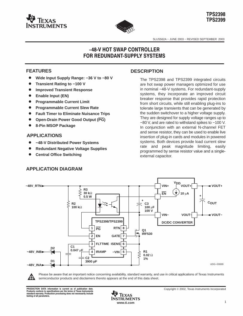
APPLICATION DIAGRAM
UDG−03069
COUT
VDD
R10.02 Ω1%
C10.047 µF
R330 kΩ0.5 W
R2100 kΩ
1
2
8
5
RTN
EN
+
−VIN
GATE
ISENS
−48V_INA
TPS2398/TPS2399
3 FLTTIME
4 IRAMP
6
7
C23900 pF
VOUT+VIN+
VOUT−
DC/DC CONVERTER
VIN−
VOUT+
VOUT−
+
D1
D2−48V_INB
−48V_RTN
Q1IRF530
C3100 µF100 V
PG
10 µAEN
!"# $ %&'# "$ (&)*%"# +"#',+&%#$ %! # $('%%"#$ (' #-' #'!$ '."$ $#&!'#$$#"+"+ /""#0, +&%# (%'$$1 +'$ # '%'$$"*0 %*&+'#'$#1 "** (""!'#'$,
Copyright 2002, Texas Instruments Incorporated
Please be aware that an important notice concerning availability, standard warranty, and use in critical applications of Texas Instrumentssemiconductor products and disclaimers thereto appears at the end of this data sheet.

SLUS562A − JUNE 2003 − REVISED SEPTEMBER 2003
2 www.ti.com
DESCRIPTION (continued)
They also provide single-line fault reporting, electrical isolation of faulty cards, and protection against nuisanceovercurrent trips. The TPS2398 latches off in response to current faults, while the TPS2399 periodically retriesthe load in the event of a fault.
ABSOLUTE MAXIMUM RATINGS (See Note 1)
TPS2398/1 UNIT
Input voltage range, all pins except RTN, EN, PG(2) −0.3 V to 15 V
Input voltage range, RTN(2) −0.3 V to 100 V
Input voltage range, EN(2)(3) −0.3 V to 100 V
Output voltage range, PG(2)(4) −0.3 V to 100 V
Continuous output current, PG 10 mA
Continuous total power dissipation see Dissipation Rating Table
Operating junction temperature range, TJ −55C to 125C C
Storage temperature range, Tstg −65C to 150C C
Lead temperature soldering 1,6 mm (1/16 inch) from case for 10 seconds 260C C
NOTES 1: Stresses beyond those listed under ”absolute maximum ratings” may cause permanent damage to the device. These are stress ratingsonly and functional operation of the device at these or any other conditions beyond those indicated under ”recommended operatingconditions” is not implied. Exposure to absolute−maximum−rated conditions for extended periods may affect device reliability.
2: All voltages are with respect to −VIN (unless otherwise noted).3: With 100-kΩ minimum input series resistance, −0.3 V to 15 V with low impedance.4: With 10-kΩ minimum series resistance, −0.3 V to 80 V with low impedance.
ELECTROSTATIC DISCHARGE (ESD) PROTECTION
MIN UNIT
Human Body Model (HBM) 1.5 kV
Charged Device Model (CDM) 1.5 kV
RECOMMENDED OPERATING CONDITIONS†
MIN NOM MAX UNIT
Nominal input supply, −VIN to RTN −80 −36 V
Operating junction temperature range −40 85 C† All voltages are with respect to −VIN (unless otherwise noted)
DISSIPATION RATING TABLE
PACKAGE TA < 25CPOWER RATING
DERATING FACTORABOVE TA = 25C
TA = 85CPOWER RATING
MSOP-8 420 mW 4.3 mW/C 160 mW
AVAILABLE OPTIONS
OPERATING FAULT PACKAGED DEVICESOPERATINGTA
FAULTOPERATION
PACKAGED DEVICESMSOP (DGK)
−40C to 85CLatch off TPS2398DGK
−40C to 85CPeriodically retry TPS2399DGK

SLUS562A − JUNE 2003 − REVISED SEPTEMBER 2003
3www.ti.com
ELECTRICAL CHARACTERISTICS
VI(−VIN) = −48 V with respect to RTN, VI(EN) = 2.8 V, VI(ISENS) = 0, all outputs unloaded, TA = −40C to 85C (unless otherwise noted)(1)(2)
input supplyPARAMETER TEST CONDITIONS MIN TYP MAX UNIT
ICC1 Supply current, RTN VI(RTN) = 48 V 700 1000 µA
ICC2 Supply current, RTN VI(RTN) = 80 V 1000 1500 µA
VUVLO_L UVLO threshold, input voltage rising To GATE pull-up, referenced to RTN −36 −30 −25 V
VHYS UVLO hysteresis 1.8 2.3 3.0 V
enable input (EN)
PARAMETER TEST CONDITIONS MIN TYP MAX UNIT
VTH Threshold voltage, input voltage rising To GATE pull-up 1.3 1.4 1.5 V
VHYS_EN EN hysteresis 22 60 90 mV
IIH High-level input current VI(EN) = 5 V −2 1 2 µA
linear current amplifier (LCA)
PARAMETER TEST CONDITIONS MIN TYP MAX UNIT
VOH High-level output, GATE VI(ISENS) = 0 V 11 14 17 V
ISINK Output sink current VI(ISENS) = 80 mV, VO(GATE) = 5V, Fault mode 50 100 mA
II Input current, ISENS 0 V < VI(ISENS) < 0.2 V −1 1 µA
VREF_K Reference clamp voltage VO(IRAMP) = open 33 40 46 mV
VIO Input offset voltage VO(IRAMP) = 2 V −7 6 mV
ramp generator
PARAMETER TEST CONDITIONS MIN TYP MAX UNIT
ISRC1 IRAMP source current, slow turn-on rate VO(IRAMP) = 0.25 V −850 −600 −400 nA
ISRC2 IRAMP source current, normal rate VO(IRAMP) = 1 V, 3 V −11 −10 −9 µA
VOL Low-level output voltage VI(EN) = 0 V 5 mV
AV Voltage gain, relative to ISENS VO(IRAMP) = 1 V, 3 V 9.5 10.0 10.5 mV/V
overload comparator
PARAMETER TEST CONDITIONS MIN TYP MAX UNIT
VTH_OL Current overload threshold, ISENS 80 100 120 mV
tDLY Glitch filter delay time VI(ISENS) = 200 mV 2 4 7 µs
fault timer
PARAMETER TEST CONDITIONS MIN TYP MAX UNIT
VOL Low-level output voltage VI(EN) = 0 V 5 mV
ICHG Charging current, current limit mode VI(ISENS) = 80 mV, VO(FLTTIME) = 2 V −55 −50 −45 µA
VFLT Fault threshold voltage 3.75 4.00 4.25 V
IDSG Discharge current, retry mode TPS2399 VI(ISENS) = 80 mV, VO(FLTTIME) = 2 V 0.38 0.75 µA
D Output duty cycle TPS2399 1 1.5 %
IRST Discharge current, timer reset mode VO(FLTTIME) = 2 V, VI(ISENS) = 0 V 1 mA
NOTES 1: All voltages are with respect to the −VIN terminal unless otherwise stated.2: Currents are positive into and negative out of the specified terminal.

SLUS562A − JUNE 2003 − REVISED SEPTEMBER 2003
4 www.ti.com
ELECTRICAL CHARACTERISTICS (continued)
VI(−VIN) = −48 V with respect to RTN, VI(EN) = 2.8 V, VI(ISENS) = 0, all outputs unloaded, TA = −40C to 85C (unless otherwise noted)(1)(2)
PG output
PARAMETER TEST CONDITIONS MIN TYP MAX UNIT
IOH High-level output (leakage) current VI(EN) = 0 V, VO(PG) = 65 V 10 µA
RDS(ON) Driver ON resistance VI(ISENS) = 80 mV, VO(FLTTIME) = 5V,
IO(PG) = 1 mA
35 80 Ω
NOTES 1: All voltages are with respect to the −VIN terminal unless otherwise stated.2: Currents are positive into and negative out of the specified terminal.
TERMINAL FUNCTIONS
TERMINAL I/O DESCRIPTION
NAME NO.
EN 2 I Enable input to turn on/off power to the load.
PG 1 O Open-drain, active-low indication of a load power good condition.
FLTTIME 3 I/O Connection for user-programming of the fault timeout period.
GATE 7 O Gate drive for external N-channel FET.
IRAMP 4 I/O Programming input for setting the inrush current slew rate.
ISENS 6 I Current sense input.
RTN 8 I Positive supply input for the TPS2398 and TPS2399.
−VIN 5 I Negative supply input and reference pin for the TPS2398 and TPS2399.
DGK PACKAGE(TOP VIEW)
1 8
2
3
4
7
6
5
EN
FLTTIME
IRAMP
RTN
GATE
ISENS
−VIN
PG

SLUS562A − JUNE 2003 − REVISED SEPTEMBER 2003
5www.ti.com
DETAILED PIN DESCRIPTIONS
EN: Enable input to turn on/off power to the load. The EN pin is referenced to the −VIN potential of the circuit.When this input is pulled high (above the nominal 1.4-V threshold) the device enables the GATE output, andbegins the ramp of current to the load. When this input is low, the linear current amplifier (LCA) is disabled, anda large pull-down device is applied to the FET gate, disabling power to the load.
FLTTIME: Connection for user-programming of the fault timeout period. An external capacitor connected fromFLTTIME to −VIN establishes the timeout period to declare a fault condition. This timeout protects againstindefinite current sourcing into a faulted load, and also provides a filter against nuisance trips from momentarycurrent spikes or surges. The TPS2398 and TPS2399 define a fault condition as voltage at the ISENS pin ator greater than the 40-mV fault threshold. When a fault condition exists, the timer is active. The devices managefault timing by charging the external capacitor to the 4-V fault threshold, then subsequently discharging it to resetthe timer (TPS2398), or discharging it at approximately 1% the charge rate to establish the duty cycle for retryingthe load (TPS2399). Whenever the internal fault latch is set (timer expired), the pass FET is rapidly turned off,and the PG output is deasserted.
GATE: Gate drive for external N-channel FET. When enabled, and the input supply is above the UVLOthreshold, the gate drive is enabled and the device begins charging an external capacitor connected to theIRAMP pin. This pin voltage is used to develop the reference voltage at the non-inverting input of the internalLCA. The inverting input is connected to the current sense node, ISENS. The LCA acts to slew the pass FETgate to force the ISENS voltage to track the reference. The reference is internally clamped at 40 mV, so themaximum current that can be sourced to the load is determined by the sense resistor value as IMAX ≤ 40mV/RSENSE. Once the load voltage has ramped up to the input dc potential, and current demand drops off, theLCA drives the GATE output to about 14 V to fully enhance the pass FET, completing the low-impedance supplyreturn path for the load.
IRAMP: Programming input for setting the inrush current slew rate. An external capacitor connected betweenthis pin and −VIN establishes the load current slew rate whenever power to the load is enabled. The devicecharges the external capacitor to establish the reference input to the LCA. The closed-loop control of the LCAand pass FET acts to maintain the current sense voltage at ISENS at the reference potential. Since the sensevoltage is developed as the drop across a resistor, the charging current ramp rate is set by the voltage ramprate at the IRAMP pin. When the output is disabled via the EN input or due to a load fault, the capacitor isdischarged and held low to initialize for the next turn-on.
ISENS: Current sense input. An external low value resistor connected between this pin and −VIN is used to feedback current magnitude information to the TPS2398/99. There are two internal device thresholds associatedwith the voltage at the ISENS pin. During charging of the load’s input capacitance, or during other periods ofexcessive demand, the HSPM acts to limit this voltage to 40 mV. Whenever the LCA is in current regulationmode, the capacitor at FLTTIME is charged to activate the timer. If, when the LCA is driving to its supply rail,a fast-acting fault such as a short-circuit, causes the ISENS voltage to exceed 100 mV (the overload threshold),the GATE pin is pulled low rapidly, bypassing the fault timer.
PG: Open-drain, active-low indication of load power good. A power good status is declared when the outputis enabled, the GATE pin voltage has ramped to at least 7 V, and the voltage on the IRAMP pin exceedsapproximately 5 V. This last condition assures that full programmed sourcing current is available prior todeclaring power good, even with very slow current ramp rates. This additional protection prevents potentialdischarging of the module input bulk capacitance during load turn-on.
RTN: Positive supply input for the TPS2398/99. For negative voltage systems, the supply pin connects directlyto the return node of the input power bus. Internal regulators step down the input voltage to generate the varioussupply levels used by the TPS2398 and TPS2399.
−VIN: Negative supply input and reference pin for the TPS2398/99. This pin connects directly to the input supplynegative rail. The input and output pins and all internal circuitry are referenced to this pin, so it is essentially theGND or VSS pin of the device.
SLUS562A − JUNE 2003 − REVISED SEPTEMBER 2003
6 www.ti.com
TYPICAL CHARACTERISTICS
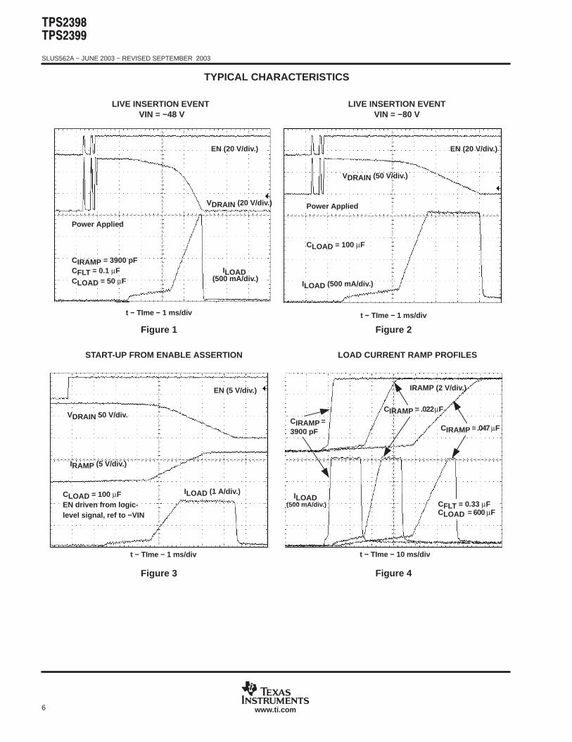
Figure 1
LIVE INSERTION EVENT VIN = −48 V
Power Applied
CIRAMP = 3900 pFCFLT = 0.1 µFCLOAD = 50 µF
EN (20 V/div.)
VDRAIN (20 V/div.)
ILOAD (500 mA/div.)
t − TIme − 1 ms/div
Figure 2
LIVE INSERTION EVENTVIN = −80 V
ILOAD (500 mA/div.)
VDRAIN (50 V/div.)
EN (20 V/div.)
Power Applied
CLOAD = 100 µF
t − TIme − 1 ms/div
Figure 3
START-UP FROM ENABLE ASSERTION
ILOAD (1 A/div.)
VDRAIN 50 V/div.
EN (5 V/div.)
IRAMP (5 V/div.)
CLOAD = 100 µFEN driven from logic-level signal, ref to −VIN
t − TIme − 1 ms/div
Figure 4
LOAD CURRENT RAMP PROFILES
CFLT = 0.33 µFCLOAD = 600 µF
IRAMP (2 V/div.)
CIRAMP = 3900 pF CIRAMP = .047 µF
ILOAD (500 mA/div.)
CIRAMP = .022 µF
t − TIme − 10 ms/div

SLUS562A − JUNE 2003 − REVISED SEPTEMBER 2003
7www.ti.com
TYPICAL CHARACTERISTICS
Figure 5
TURN-ON INTO SHORTED LOAD(TPS2399)
ILOAD(1 A/div.)
VIRAMP (5 V/div.)
FLTTIME (2 V/div.)
CIRAMP = 3900 pFCFLT = 0.047 µFRPG = 100 kΩ
t − TIme − 1 ms/div
PG (50 V/div.)
Figure 6
TURN-ON INTO SHORTED LOAD(TPS2398)
t − TIme − 1 ms/div
ILOAD(1 A/div.)
VIRAMP (5 V/div.)
FLTTIME (2 V/div.)
CIRAMP = 3900 pFCFLT = 0.047 µFRPG = 100 kΩ
PG (50 V/div.)
Figure 7
FAULT RETRY OPERATION(TPS2399)
ILOAD (1 A/div.)
VDRAIN (20 V/div.)
FLTTIME (2 V/div.)
CIRAMP = 3900 pFCFLT = 0.047 µFCLOAD = 100 µFRLOAD = 12.5 Ω
PG (50 V/div.)
t − TIme − 50 ms/div
Figure 8
RECOVERY FROM A FAULT − LARGE SCALE VIEW(TPS2399)
ILOAD (1 A/div.)
VDRAIN (20 V/div.)
FLTTIME (2 V/div.)
CIRAMP = 3900 pFCFLT = 0.047 µFCLOAD = 100 µF
PG (50 V/div.)
t − TIme − 50 ms/div

SLUS562A − JUNE 2003 − REVISED SEPTEMBER 2003
8 www.ti.com
TYPICAL CHARACTERISTICS
Figure 9
RECOVERY FROM A FAULT − EXPANDED VIEW(TPS2399)
ILOAD (1 A/div)
VDRAIN (20 V/div)
FLTTIME (2 V/div.)
CIRAMP = 3900 pFCFLT = 0.047 µFCLOAD = 100 µF
PG (50 V/div)
t − TIme − 1 ms/div
Figure 10
PG OUTPUT TIMING,VOLTAGE QUALIFIED
CIRAMP = 3900 pFCFLT = 0.1 µFCLOAD = 150 µF
VIRAMP (2 V/div)
VDRAIN (20 V/div)
PG (50 V/div)
t − TIme − 1 ms/div
Figure 11
PG OUTPUT TIMING,CURRENT QUALIFIED
t − TIme − 1 ms/div
CIRAMP = 0.01 µFCFLT = 0.1 µFCLOAD = 50 µF
VIRAMP (2 V/div)
VDRAIN (20 V/div)
PG (50 V/div)
VTH_PG
Figure 12
SUPPLY CURRENTvs
AMBIENT TEMPERATURE
−40 −15 10 35 60 85
0
200
400
600
800
1000
1200
I CC
− S
uppl
y C
urre
nt −
µA
TA − Ambient Temperature − °C
VRTN = 48 V
VRTN = 36 V
VRTN = 80 V

SLUS562A − JUNE 2003 − REVISED SEPTEMBER 2003
9www.ti.com
TYPICAL CHARACTERISTICS
Figure 13
GATE HIGH-LEVEL OUTPUTvs
AMBIENT TEMPERATURE
−40 −15 10 35 60 85
14.0
14.5
15.0
15.5
16.0
16.5
17.0
VO
H −
Out
put V
olta
ge −
V
TA − Ambient Temperature − °C
VRTN = 80 V
VRTN = 48 V
VI(ISENS) = 0 V
VRTN = 36 V
Figure 14
IRAMP OUTPUT CURRENTvs
AMBIENT TEMPERATURE, SLOW TURN-ON
−40 −15 10 35 60 85
−066
−0.62
−0.58
−0.54
−0.50
I SR
C1
− IR
AM
P O
utpu
t Cur
rent
− µ
A
VRTN = 80 V
VRTN = 36 V
VRTN = 48 V
VO(IRAMP) = 0.25 V
TA − Ambient Temperature − °C
Figure 15
−40 −15 10 35 60 85
−10.5
−10.3
−10.1
−9.9
−9.7
−9.5
IRAMP OUTPUT CURRENTvs
AMBIENT TEMPERATURE, NORMAL RATE
I SR
C2
− IR
AM
P O
utpu
t Cur
rent
− µ
A
Average for V O(IRAMP) = 1 V, 3 VVRTN = 36 V to 80 V
TA − Ambient Temperature − °C
Figure 16
TIMER CHARGING CURRENTvs
AMBIENT TEMPERATURE
−40 −15 10 35 60 85
−55
−53
−51
−49
−47
−45
I CH
G −
Cha
rgin
g C
urre
nt −
µA
VI(ISENS) = 80 mVVO(FLTTIME) = 2 V
TA − Ambient Temperature − °C
VRTN = 48 VVRTN = 36 V
VRTN = 80 V
SLUS562A − JUNE 2003 − REVISED SEPTEMBER 2003
10 www.ti.com
TYPICAL CHARACTERISTICS
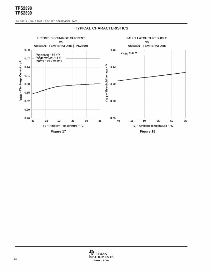
Figure 17
−40 −15 10 35 60 850.26
0.29
0.32
0.35
0.38
0.41
0.44
0.47
0.50
FLTTIME DISCHARGE CURRENTvs
AMBIENT TEMPERATURE (TPS2399)
I DS
G −
Dis
char
ge C
urre
nt −
µA
VI(ISENS) = 80 mVVO(FLTTIME) = 2 VVRTN = 36 V to 80 V
TA − Ambient Temperature − °C
Figure 18
FAULT LATCH THRESHOLDvs
AMBIENT TEMPERATURE
−40 −15 10 35 60 853.75
3.88
4.00
4.13
4.25
VF
LT −
Thr
esho
ld V
olta
ge −
V
VRTN = 48 V
TA − Ambient Temperature − °C

SLUS562A − JUNE 2003 − REVISED SEPTEMBER 2003
11www.ti.com
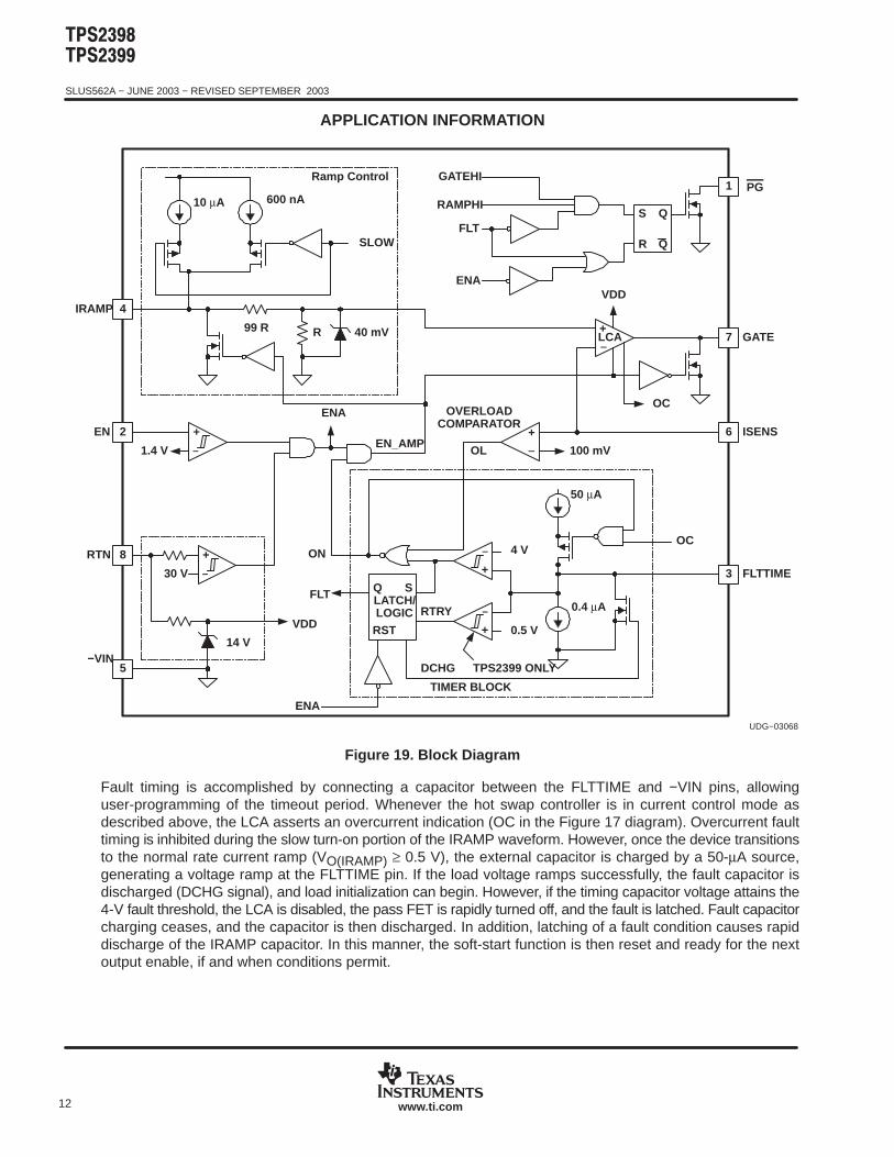
APPLICATION INFORMATION
When a plug-in module or printed circuit card is inserted into a live chassis slot, discharged supply bulkcapacitance on the board can draw huge transient currents from the system supplies. Without some form ofinrush limiting, these currents can reach peak magnitudes ranging up to several hundred amps, particularly inhigh-voltage systems. Such large transients can damage connector pins, PCB etch, and plug-in and supplycomponents. In addition, current spikes can cause voltage droops on the power distribution bus, causing otherboards in the system to reset.
The TPS2398 and TPS2399 are hot swap power managers designed to limit these peaks to preset levels, aswell as control the slew rate (di/dt) at which charging current ramps to the user-programmed limit. These devicesuse an external N-Channel pass FET and sense element to provide closed-loop control of current sourced tothe load. Input supply undervoltage lockout (UVLO) protection allows hot swap circuits to turn on automaticallywith the application of power, or to be controlled with a system command via the EN input. External capacitorscontrol both the current ramp rate, and the time−out period for load voltage ramping. In addition, an internaloverload comparator provides circuit breaker protection against shorts occurring during steady-state(post-turn-on) operation of the card.
The TPS2398 and TPS2399 operate directly from the input supply (nominal −48 VDC rail). The −VIN pinconnects to the negative voltage rail, and the RTN pin connects to the supply return. Internal regulators convertinput power to the supply levels required by the device circuitry. An input UVLO circuit holds the GATE outputlow until the supply voltage reaches a nominal 30-V level. A second comparator monitors the EN input; this pinmust be pulled above the 1.4-V enable threshold to turn on power to the load.
Once enabled, and when the input supply is above the UVLO threshold, the GATE pull-down is removed, thelinear control amplifier (LCA) is enabled, and a large discharge device in the RAMP CONTROL block is turnedoff. Subsequently, a small current source is now able to charge an external capacitor connected to the IRAMPpin. This results in a linear voltage ramp at IRAMP. The voltage ramp on the capacitor actually has two discreteslopes. As shown in Figure 17, charging current is supplied from either of two sources. Initially at turn-on, the600-nA source is selected, to provide a slow turn-on rate. This slow turn-on helps ensure that the LCA is pulledout of saturation, and is slewing to the voltage at its non-inverting input before normal rate load charging isallowed. This mechanism helps reduce current steps at turn-on. Once the voltage at the IRAMP pin reachesapproximately 0.5 V, an internal comparator deasserts the SLOW signal, and the 10-µA source is selected forthe remainder of the ramp period.
The voltage at IRAMP is divided down by a factor of 100, and applied to the non-inverting input of the LCA. Loadcurrent magnitude information at the ISENS pin is applied to the inverting input. This voltage is developed byconnecting the current sense resistor between ISENS and −VIN. The LCA slews the gate of the external passFET to force the ISENS voltage to track the divided down IRAMP voltage. Consequently, the load current slewrate tracks the linear voltage ramp at the IRAMP pin, producing a linear di/dt of the load current. The IRAMPcapacitor is charged to about 6.5 V; however, the LCA input is clamped at 40 mV. Therefore, the current sourcedto the load during turn-on is limited to a value given by IMAX ≤ 40 mV/RSENSE, where RSENSE is the value ofthe sense resistor.
The resultant load current, regulated by the controller, charges the module’s input bulk capacitance in a safefashion. Under normal conditions, this capacitance eventually charges up to the dc input potential. At this point,the load demand drops off, and the voltage at ISENS decreases. The LCA now drives the GATE output to itssupply rail.
The device detects this condition as the GATE voltage rises through 7 V or 8 V, latches this status and assertsthe PG output. If the full sourced current limit is not yet available to the load, as evidenced by the IRAMP voltagebeing less than 5 V, then the PG assertion is delayed until that condition is also met.
The peak, steady-state GATE pin output, typically 14 V, ensures sufficient overdrive to fully enhance the externalFET, while not exceeding the typical 20-V VGS rating of common N-channel power FETs.
SLUS562A − JUNE 2003 − REVISED SEPTEMBER 2003
12 www.ti.com
APPLICATION INFORMATION
RAMPHI
1
7
6
3
4
2
8
5
IRAMP
EN
RTN
−VIN
GATE
ISENS
FLTTIME
+
1.4 V
600 nA
SLOW
99 R R 40 mV
ENA
+
30 V
EN_AMP
+LCA
VDD
OC
+
100 mV
+
LATCH/LOGIC
Q S
RST +
ENA
RTRY
4 V
0.5 V
TIMER BLOCK
DCHG TPS2399 ONLY
OL
OVERLOADCOMPARATOR
S Q
QR
GATEHI
ENA
FLT
OC
UDG−03068
10 µA
50 µA
0.4 µAVDD
Ramp Control
14 V
FLT
PG
ON
Figure 19. Block Diagram
Fault timing is accomplished by connecting a capacitor between the FLTTIME and −VIN pins, allowinguser-programming of the timeout period. Whenever the hot swap controller is in current control mode asdescribed above, the LCA asserts an overcurrent indication (OC in the Figure 17 diagram). Overcurrent faulttiming is inhibited during the slow turn-on portion of the IRAMP waveform. However, once the device transitionsto the normal rate current ramp (VO(IRAMP) ≥ 0.5 V), the external capacitor is charged by a 50-µA source,generating a voltage ramp at the FLTTIME pin. If the load voltage ramps successfully, the fault capacitor isdischarged (DCHG signal), and load initialization can begin. However, if the timing capacitor voltage attains the4-V fault threshold, the LCA is disabled, the pass FET is rapidly turned off, and the fault is latched. Fault capacitorcharging ceases, and the capacitor is then discharged. In addition, latching of a fault condition causes rapiddischarge of the IRAMP capacitor. In this manner, the soft-start function is then reset and ready for the nextoutput enable, if and when conditions permit.
SLUS562A − JUNE 2003 − REVISED SEPTEMBER 2003
13www.ti.com
APPLICATION INFORMATION
Subsequent to a plug-in’s start-up, and during the module’s steady-state operation, load faults that force currentlimit operation also initiate fault timing cycles as described above. In this case, a fault timeout also clears thepreviously latched power good status.
The TPS2398 latches off in response to faults; once a fault timeout occurs, the DCHG signal turns on a largeNMOS device to rapidly discharge the external capacitor, resetting the timer for any subsequent device reset.The TPS2398 can only be reset by cycling power to the device, or by cycling the EN input.
In response to a latched fault condition, the TPS2399 enters a fault retry mode, wherein it periodically retriesthe load to test for continued existence of the fault. In this mode, the FLTTIME capacitor is discharged slowlyby a about a 0.4-µA constant-current sink. When the voltage at the FLTTIME pin decays below 0.5 V, the LCAand RAMP CONTROL circuits are re-enabled, and a normal turn-on current ramp ensues. Again, during theload charging, the OC signal causes charging of the FLTTIME capacitor until the next delay period elapses. Thesequential charging and discharging of the FLTTIME capacitor results in a typical 1% retry duty cycle. If the faultsubsides, the timing capacitor is rapidly discharged, duty-cycle operation stops, and the PG output is asserted.
Note that because of the timing inhibit during the initial slow ramp period, the duty cycle in practice is slightlygreater than the nominal 1% value. However, sourced current during this period peaks at only about one-eighththe maximum limit. The duty cycle of the normal ramp and constant-current periods is approximately 1%.
The FAULT LOGIC within the TIMER BLOCK automatically manages capacitor charge and discharge actions,and the enabling of the GATE output (DCHG and ON signals).
supply transient response
The TPS2398 and TPS2399 also feature a fast-acting overload comparator which acts to clamp large transientsfrom catastrophic faults occurring once the pass FET is fully enhanced, such as short circuits. This functionprovides a back-up protection to the LCA by providing a hard gate discharge action when the LCA is saturated.If sense voltage excursions above 100 mV are detected, this comparator rapidly pulls down the GATE output,bypassing the fault timer, and terminating the short−circuit condition. Once the spike has been brought downbelow the overload threshold, the GATE output is released, allowing the circuit to turn on again in eithercurrent-ramp or current-limit mode. A 4−µs deglitch filter is applied to the OL signal to help reduce theoccurrence of nuisance trips.
In redundant-supply systems, the sudden switchover to a supply of higher voltage potential is one more sourceof large current spikes. Due to the low impedance of filter capacitance under such high-frequency transients,these spikes are generally indistinguishable from true short-circuit faults to a hot swap controller. However, theTPS2398and TPS2399 transient response addresses this issue by providing rapid circuit-breaker protectionfor load faults along with minimal interruption of power flow during supply switching events. The scope plots inFigure 20 illustrate how.
Figure 20 is a scope capture of the TPS2398/99 response in a diode-OR configuration to such an input transientevent. (All waveforms are referenced to the −VIN pin.) In this example, the module is initially operating froma nominal −44-V supply (relative to the backplane supply return node). At the second major time division,another power supply, with an output of −48 V, is suddenly hot swapped into a secondary, or INB, input. Thissudden voltage step is reflected in the −48V_RTN trace. On this board, the 4−V potential difference causeda greater than 6-A spike, as shown by the IINB trace. The GATE pin is rapidly pulled low, which quickly terminatesthe overload spike. However, it is quickly released, and seen to drive back to the pass FET ON-threshold, inthis case, about 4.5 V. The resultant current-limit operation of the circuit is evidenced by the 2-A load on the Bsupply. Once supply current is flowing again, the filter capacitance is charged up to the new input supply level,seen here on the VDRAIN trace. Once the capacitance is fully charged, the load demand rolls off to the operating1-A level. As an added benefit, this event is transparent to the PG signal, which remains asserted throughoutthe disturbance.

SLUS562A − JUNE 2003 − REVISED SEPTEMBER 2003
14 www.ti.com
APPLICATION INFORMATION
Figure 20
INPUT TRANSIENT RESPONSE
CLOAD = 100 µFRLOAD = 50 Ω RSNS = 20 mΩCIRAMP = 3900 pF
IINB= (2 A/div)
−48V_RTN (5 V/div)(Offset 44 V)
t − TIme − 100 µs/div
GATE (5 V/div)
VDRAIN (5 V/div)
PG (50 V/div)
In order for downstream loads (bricks, etc.) to operate through the distribution bus transient, it is important toproperly size the filtering capacitance to supply the needed energy during the OFF-time of the pass FET. In thisexample, once the RTN node stabilizes at about 3.5 V higher than the original potential, about 4.5 V developsacross the FET, indicating approximately a 1-V droop across the brick input. Therefore, due to the fast responseof the TPS2398/99 devices, the 100-µF capacitor achieves excellent hold-up of the brick input voltage. Actualrequirements depend heavily on the individual application. Whether the device turns back on in eithercurrent-ramp or current-limit mode depends in part on the size of the ramp capacitor (CIRAMP) and the inputcapacitance of the pass FET. But in any case, the circuit turns back on in a controlled-current manner afterrapidly clamping the potentially damaging spike.
SLUS562A − JUNE 2003 − REVISED SEPTEMBER 2003
15www.ti.com
APPLICATION INFORMATION
setting the sense resistor value
Due to the current-limiting action of the internal LCA, the maximum allowable load current for an implementationis easily programmed by selecting the appropriate sense resistor value. The LCA acts to limit the sense voltageVI(ISENS) to its internal reference. Once the voltage at the IRAMP pin exceeds approximately 4 V, this limit isthe clamp voltage, VREF_K. Therefore, a maximum sense resistor value can be determined from equation (1).
RSENSE 33 mVIMAX
where:
• RSENSE is the resistor value, and
• IMAX is the desired current limit.
When setting the sense resistor value, it is important to consider two factors, the minimum current that may beimposed by the TPS2398 or TPS2399, and the maximum load under normal operation of the module. For thefirst factor, the specification minimum clamp value is used, as seen in equation (1). This method accounts forthe tolerance in the sourced current limit below the typical level expected (40 mV/RSENSE). (The clampmeasurement includes LCA input offset voltage; therefore, this offset does not have to be factored into thecurrent limit again.) Second, if the load current varies over a range of values under normal operating conditions,then the maximum load level must be allowed for by the value of RSENSE. One example of this is when the loadis a switching converter, or brick, which draws higher input current, for a given power output, when thedistribution bus is at the low end of its operating range, with decreasing draw at higher supply voltages. To avoidcurrent-limit operation under normal loading, some margin should be designed in between this maximumanticipated load and the minimum current limit level, or IMAX > ILOAD(max), for equation (1).
For example, using a 20-mΩ sense resistor for a nominal 1-A load application provides a minimum of 650 mAof overhead for load variance/margin. Typical bulk capacitor charging current during turn-on is 2 A(40 mV/20 mΩ).
setting the inrush slew rate
The TPS2398 and TPS2399 devices enable user-programming of the maximum current slew rate during loadstart-up events. A capacitor tied to the IRAMP pin (C2 in the typical application diagram) controls the di/dt rate.Once the sense resistor value has been established, a value for ramp capacitor CIRAMP, in microfarads, can bedetermined from equation (2).
CIRAMP 11
100 RSENSE didt
MAX
where:
• RSENSE is in ohms, and
• (di/dt)MAX is the desired maximum slew rate, in amperes/second.
For example, if the desired slew rate for the typical application shown is 1500 mA/ms, the calculated value forCIRAMP is about 3700 pF. Selecting the next larger standard value of 3900 pF (as shown in the diagram) providessome margin for capacitor and sense resistor tolerances.
(1)
(2)
SLUS562A − JUNE 2003 − REVISED SEPTEMBER 2003
16 www.ti.com
APPLICATION INFORMATION
As described earlier in this section, the TPS2398 and TPS2399 initiate ramp capacitor charging, andconsequently, load current di/dt at a reduced rate. This reduced rate applies until the voltage on the IRAMP pinis about 0.5 V. The maximum di/dt rate, as set by equation (2), is effective once the device has switched to the10-µA charging source.
setting the fault timing capacitor
The fault timeout period is established by the value of the capacitor connected to the FLTTIME pin, CFLT. Thetimeout period permits riding out spurious current glitches and surges that may occur during operation of thesystem, and prevents indefinite sourcing into faulted loads swapped into a live system. However, to ensuresmooth voltage ramping under all conditions of load capacitance and input supply potential, the minimumtimeout should be set to accommodate these system variables. To do this, a rough estimate of the maximumvoltage ramp time for a completely discharged plug-in card provides a good basis for setting the minimum timerdelay.
Due to the three-phase nature of the load current at turn-on, the load voltage ramp potentially has three distinctphases ( compare Figures 1 and 2). This profile depends on the relative values of load capacitance, input dcpotential, maximum current limit and other factors. The first two phases are characterized by the two differentslopes of the current ramp; the third phase, if required for bulk capacitance charging, is the constant-currentcharging at IMAX. Considering the two current ramp phases to be one period at an average di/dt simplifiescalculation of the required timing capacitor.
For the TPS2398 and TPS2399, the typical duration of the soft-start ramp period, tSS, is given by equation (3).
tSS 1183 CIRAMP
where:
• tSS is the soft-start period in ms, and
• CIRAMP is given in µF
During this current ramp period, the load voltage magnitude which is attained is estimated by equation (4).
VLSS iAVG
2 CLOAD CIRAMP 100 RSENSE tSS
2
where:
• VLSS is the load voltage reached during soft-start,
• iAVG is 3.38 µA for the TPS2398 and TPS2399,
• CLOAD is the amount of the load capacitance, and
• tSS is the soft-start period, in seconds
The quantity iAVG in equation (4) is a weighted average of the two charge currents applied to CIRAMP duringturn-on, considering the typical output values.
(3)
(4)

SLUS562A − JUNE 2003 − REVISED SEPTEMBER 2003
17www.ti.com
APPLICATION INFORMATION
If the result of equation (4) is larger than the maximum input supply value, then the load can be expected tocharge completely during the inrush slewing portion of the insertion event. However, if this voltage is less thanthe maximum supply input, VIN(max), the HSPM transitions to the constant-current charging of the load. Theremaining amount of time required at IMAX is determined from equation (5).
tCC CLOAD VIN (max) VLSS
VREF_K (min)RSENSE
where:
• tCC is the constant-current voltage ramp time, in seconds, and
• VREF_K(min) is the minimum clamp voltage, 33 mV.
With this information, the minimum recommended value timing capacitor CFLT can be determined. The delaytime needed will be either a time tSS2 or the sum of tSS2 and tCC, according to the estimated time to charge theload. The quantity tSS2 is the duration of the normal rate current ramp period, and is given by equation (6).
tSS2 0.35 CRAMP
where:
• CRAMP is given in microfarads
Since fault timing is generated by the constant−current charging of CFLT, the capacitor value is determined fromeither equation (7) or (8), as appropriate.
CFLT(min) 55 tSS2
3.75
CFLT(min) 55 tSS2 tCC
3.75
where:
• CFLT(min) is the recommended capacitor value, in microfarads,
• tSS2 is the result of equation (6), in seconds, and
• tCC is the result of equation (5), in seconds.
Continuing the typical application example, using a 100-µF input capacitor (CLOAD), equations (3) and (4)estimate the load voltage ramping to approximately −46 V during the soft-start period. If the module shouldoperate down to −72 V input supply, approximately another 1.58-ms of constant-current charging may berequired. Therefore, equations (6) and (8) are used to determine CFLT(min), and the result of 0.043-µF suggeststhe 0.047-µF standard value.
(5)
(6)
(7)
(8)

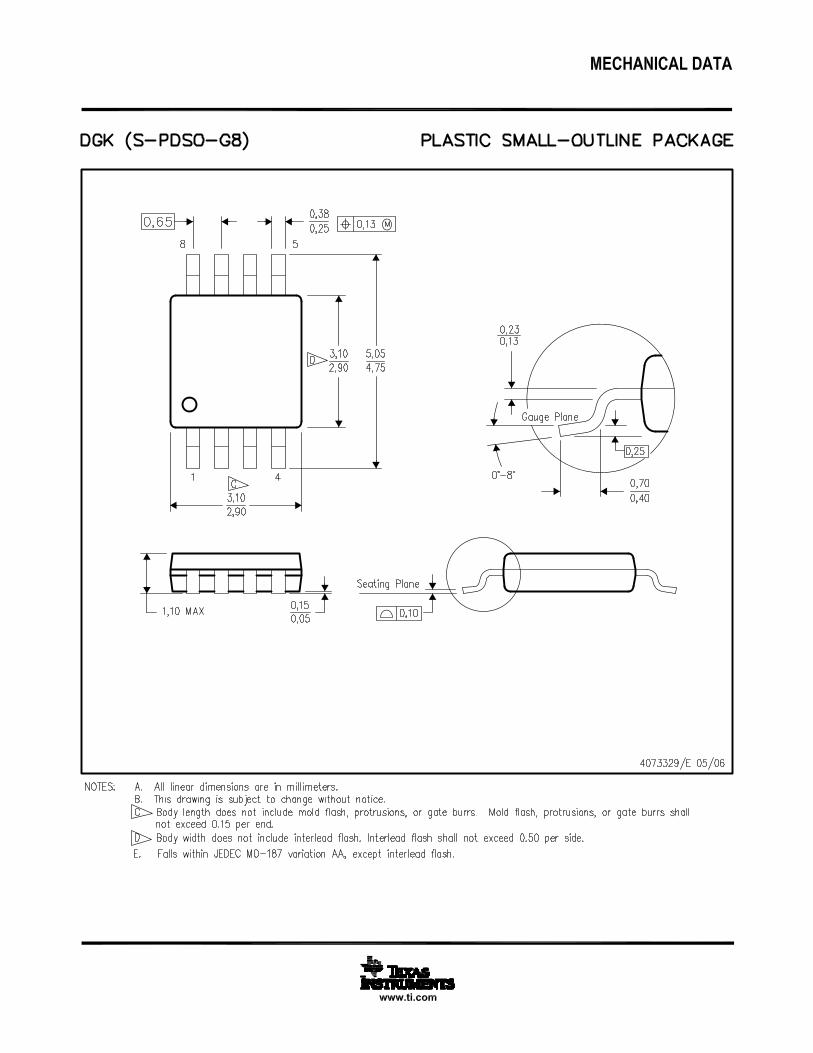
PACKAGING INFORMATION
Orderable Device Status (1) PackageType
PackageDrawing
Pins PackageQty
Eco Plan (2) Lead/Ball Finish MSL Peak Temp (3)
TPS2398DGK ACTIVE MSOP DGK 8 80 Green (RoHS &no Sb/Br)
CU NIPDAU Level-1-260C-UNLIM
TPS2398DGKG4 ACTIVE MSOP DGK 8 80 Green (RoHS &no Sb/Br)
CU NIPDAU Level-1-260C-UNLIM
TPS2398DGKR ACTIVE MSOP DGK 8 2500 Green (RoHS &no Sb/Br)
CU NIPDAU Level-1-260C-UNLIM
TPS2398DGKRG4 ACTIVE MSOP DGK 8 2500 Green (RoHS &no Sb/Br)
CU NIPDAU Level-1-260C-UNLIM
TPS2399DGK ACTIVE MSOP DGK 8 80 Green (RoHS &no Sb/Br)
CU NIPDAU Level-2-260C-1 YEAR
TPS2399DGKG4 ACTIVE MSOP DGK 8 80 Green (RoHS &no Sb/Br)
CU NIPDAU Level-2-260C-1 YEAR
TPS2399DGKR ACTIVE MSOP DGK 8 2500 Green (RoHS &no Sb/Br)
CU NIPDAU Level-2-260C-1 YEAR
TPS2399DGKRG4 ACTIVE MSOP DGK 8 2500 Green (RoHS &no Sb/Br)
CU NIPDAU Level-2-260C-1 YEAR
(1) The marketing status values are defined as follows:ACTIVE: Product device recommended for new designs.LIFEBUY: TI has announced that the device will be discontinued, and a lifetime-buy period is in effect.NRND: Not recommended for new designs. Device is in production to support existing customers, but TI does not recommend using this part ina new design.PREVIEW: Device has been announced but is not in production. Samples may or may not be available.OBSOLETE: TI has discontinued the production of the device.
(2) Eco Plan - The planned eco-friendly classification: Pb-Free (RoHS), Pb-Free (RoHS Exempt), or Green (RoHS & no Sb/Br) - please checkhttp://www.ti.com/productcontent for the latest availability information and additional product content details.TBD: The Pb-Free/Green conversion plan has not been defined.Pb-Free (RoHS): TI's terms "Lead-Free" or "Pb-Free" mean semiconductor products that are compatible with the current RoHS requirementsfor all 6 substances, including the requirement that lead not exceed 0.1% by weight in homogeneous materials. Where designed to be solderedat high temperatures, TI Pb-Free products are suitable for use in specified lead-free processes.Pb-Free (RoHS Exempt): This component has a RoHS exemption for either 1) lead-based flip-chip solder bumps used between the die andpackage, or 2) lead-based die adhesive used between the die and leadframe. The component is otherwise considered Pb-Free (RoHScompatible) as defined above.Green (RoHS & no Sb/Br): TI defines "Green" to mean Pb-Free (RoHS compatible), and free of Bromine (Br) and Antimony (Sb) based flameretardants (Br or Sb do not exceed 0.1% by weight in homogeneous material)
(3) MSL, Peak Temp. -- The Moisture Sensitivity Level rating according to the JEDEC industry standard classifications, and peak soldertemperature.
Important Information and Disclaimer:The information provided on this page represents TI's knowledge and belief as of the date that it isprovided. TI bases its knowledge and belief on information provided by third parties, and makes no representation or warranty as to theaccuracy of such information. Efforts are underway to better integrate information from third parties. TI has taken and continues to takereasonable steps to provide representative and accurate information but may not have conducted destructive testing or chemical analysis onincoming materials and chemicals. TI and TI suppliers consider certain information to be proprietary, and thus CAS numbers and other limitedinformation may not be available for release.
In no event shall TI's liability arising out of such information exceed the total purchase price of the TI part(s) at issue in this document sold by TIto Customer on an annual basis.
PACKAGE OPTION ADDENDUM
www.ti.com 6-Dec-2006
Addendum-Page 1

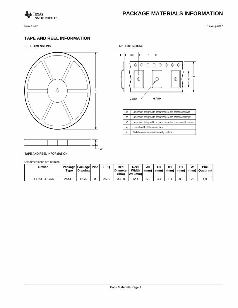
TAPE AND REEL INFORMATION
*All dimensions are nominal
Device PackageType
PackageDrawing
Pins SPQ ReelDiameter
(mm)
ReelWidth
W1 (mm)
A0 (mm) B0 (mm) K0 (mm) P1(mm)
W(mm)
Pin1Quadrant
TPS2398DGKR MSOP DGK 8 2500 330.0 12.4 5.3 3.4 1.4 8.0 12.0 Q1
TPS2399DGKR MSOP DGK 8 2500 330.0 12.4 5.3 3.4 1.4 8.0 12.0 Q1
PACKAGE MATERIALS INFORMATION
www.ti.com 29-Jul-2008
Pack Materials-Page 1
*All dimensions are nominal
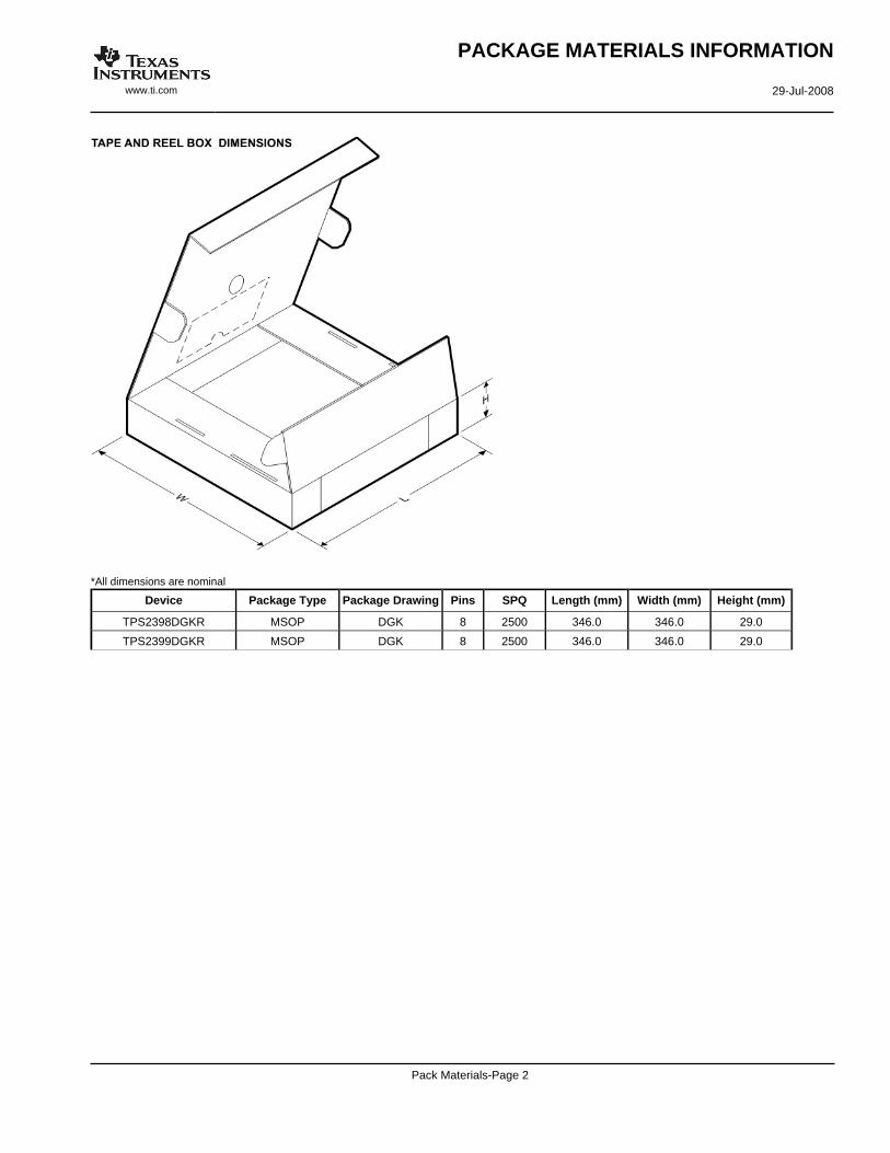
Device Package Type Package Drawing Pins SPQ Length (mm) Width (mm) Height (mm)
TPS2398DGKR MSOP DGK 8 2500 346.0 346.0 29.0
TPS2399DGKR MSOP DGK 8 2500 346.0 346.0 29.0
PACKAGE MATERIALS INFORMATION
www.ti.com 29-Jul-2008
Pack Materials-Page 2


PACKAGE OPTION ADDENDUM
www.ti.com 10-Jun-2014
Addendum-Page 1
PACKAGING INFORMATION
Orderable Device Status(1)
Package Type PackageDrawing
Pins PackageQty
Eco Plan(2)
Lead/Ball Finish(6)
MSL Peak Temp(3)
Op Temp (°C) Device Marking(4/5)
Samples
TPS2398DGK ACTIVE VSSOP DGK 8 80 Green (RoHS& no Sb/Br)
CU NIPDAUAG Level-1-260C-UNLIM -40 to 85 2398
TPS2398DGKG4 ACTIVE VSSOP DGK 8 80 Green (RoHS& no Sb/Br)
CU NIPDAUAG Level-1-260C-UNLIM -40 to 85 2398
TPS2398DGKR OBSOLETE VSSOP DGK 8 TBD Call TI Call TI -40 to 85 2398
TPS2398DGKRG4 OBSOLETE VSSOP DGK 8 TBD Call TI Call TI -40 to 85
TPS2399DGK ACTIVE VSSOP DGK 8 80 Green (RoHS& no Sb/Br)
CU NIPDAUAG Level-2-260C-1 YEAR -40 to 85 2399
TPS2399DGKG4 ACTIVE VSSOP DGK 8 80 Green (RoHS& no Sb/Br)
CU NIPDAUAG Level-2-260C-1 YEAR -40 to 85 2399
TPS2399DGKR ACTIVE VSSOP DGK 8 2500 Green (RoHS& no Sb/Br)
CU NIPDAUAG Level-2-260C-1 YEAR -40 to 85 2399
(1) The marketing status values are defined as follows:ACTIVE: Product device recommended for new designs.LIFEBUY: TI has announced that the device will be discontinued, and a lifetime-buy period is in effect.NRND: Not recommended for new designs. Device is in production to support existing customers, but TI does not recommend using this part in a new design.PREVIEW: Device has been announced but is not in production. Samples may or may not be available.OBSOLETE: TI has discontinued the production of the device.
(2) Eco Plan - The planned eco-friendly classification: Pb-Free (RoHS), Pb-Free (RoHS Exempt), or Green (RoHS & no Sb/Br) - please check http://www.ti.com/productcontent for the latest availabilityinformation and additional product content details.TBD: The Pb-Free/Green conversion plan has not been defined.Pb-Free (RoHS): TI's terms "Lead-Free" or "Pb-Free" mean semiconductor products that are compatible with the current RoHS requirements for all 6 substances, including the requirement thatlead not exceed 0.1% by weight in homogeneous materials. Where designed to be soldered at high temperatures, TI Pb-Free products are suitable for use in specified lead-free processes.Pb-Free (RoHS Exempt): This component has a RoHS exemption for either 1) lead-based flip-chip solder bumps used between the die and package, or 2) lead-based die adhesive used betweenthe die and leadframe. The component is otherwise considered Pb-Free (RoHS compatible) as defined above.Green (RoHS & no Sb/Br): TI defines "Green" to mean Pb-Free (RoHS compatible), and free of Bromine (Br) and Antimony (Sb) based flame retardants (Br or Sb do not exceed 0.1% by weightin homogeneous material)
(3) MSL, Peak Temp. - The Moisture Sensitivity Level rating according to the JEDEC industry standard classifications, and peak solder temperature.
(4) There may be additional marking, which relates to the logo, the lot trace code information, or the environmental category on the device.
(5) Multiple Device Markings will be inside parentheses. Only one Device Marking contained in parentheses and separated by a "~" will appear on a device. If a line is indented then it is a continuationof the previous line and the two combined represent the entire Device Marking for that device.

PACKAGE OPTION ADDENDUM
www.ti.com 10-Jun-2014
Addendum-Page 2
(6) Lead/Ball Finish - Orderable Devices may have multiple material finish options. Finish options are separated by a vertical ruled line. Lead/Ball Finish values may wrap to two lines if the finishvalue exceeds the maximum column width.
Important Information and Disclaimer:The information provided on this page represents TI's knowledge and belief as of the date that it is provided. TI bases its knowledge and belief on informationprovided by third parties, and makes no representation or warranty as to the accuracy of such information. Efforts are underway to better integrate information from third parties. TI has taken andcontinues to take reasonable steps to provide representative and accurate information but may not have conducted destructive testing or chemical analysis on incoming materials and chemicals.TI and TI suppliers consider certain information to be proprietary, and thus CAS numbers and other limited information may not be available for release.
In no event shall TI's liability arising out of such information exceed the total purchase price of the TI part(s) at issue in this document sold by TI to Customer on an annual basis.
TAPE AND REEL INFORMATION
*All dimensions are nominal
Device PackageType
PackageDrawing
Pins SPQ ReelDiameter
(mm)
ReelWidth
W1 (mm)
A0(mm)
B0(mm)
K0(mm)
P1(mm)
W(mm)
Pin1Quadrant
TPS2399DGKR VSSOP DGK 8 2500 330.0 12.4 5.3 3.4 1.4 8.0 12.0 Q1
PACKAGE MATERIALS INFORMATION
www.ti.com 17-Aug-2012
Pack Materials-Page 1
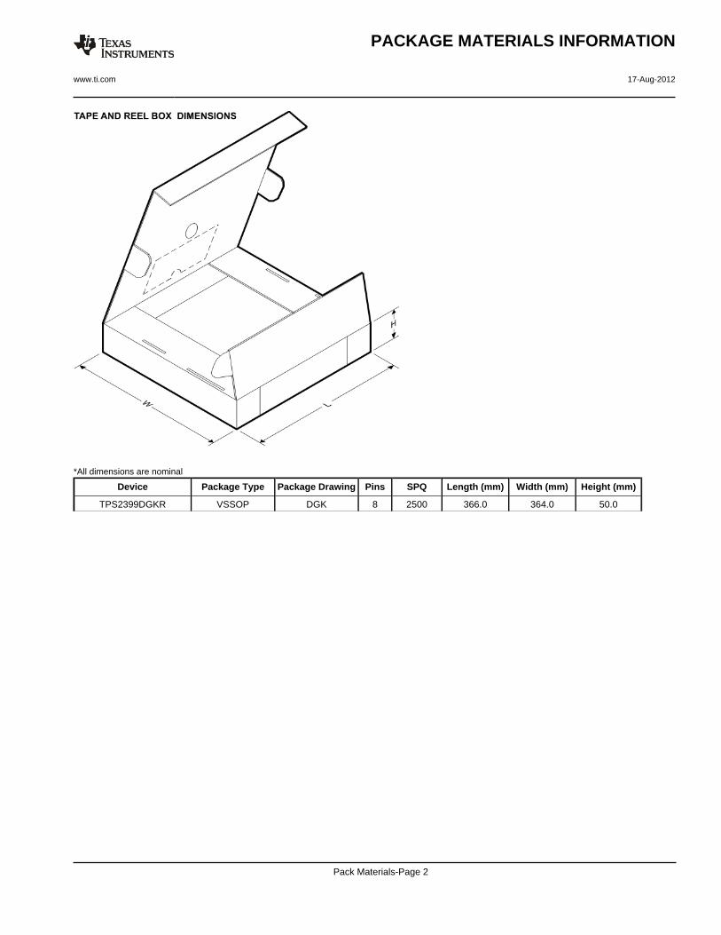
*All dimensions are nominal
Device Package Type Package Drawing Pins SPQ Length (mm) Width (mm) Height (mm)
TPS2399DGKR VSSOP DGK 8 2500 366.0 364.0 50.0
PACKAGE MATERIALS INFORMATION
www.ti.com 17-Aug-2012
Pack Materials-Page 2


IMPORTANT NOTICE
Texas Instruments Incorporated and its subsidiaries (TI) reserve the right to make corrections, enhancements, improvements and otherchanges to its semiconductor products and services per JESD46, latest issue, and to discontinue any product or service per JESD48, latestissue. Buyers should obtain the latest relevant information before placing orders and should verify that such information is current andcomplete. All semiconductor products (also referred to herein as “components”) are sold subject to TI’s terms and conditions of salesupplied at the time of order acknowledgment.TI warrants performance of its components to the specifications applicable at the time of sale, in accordance with the warranty in TI’s termsand conditions of sale of semiconductor products. Testing and other quality control techniques are used to the extent TI deems necessaryto support this warranty. Except where mandated by applicable law, testing of all parameters of each component is not necessarilyperformed.TI assumes no liability for applications assistance or the design of Buyers’ products. Buyers are responsible for their products andapplications using TI components. To minimize the risks associated with Buyers’ products and applications, Buyers should provideadequate design and operating safeguards.TI does not warrant or represent that any license, either express or implied, is granted under any patent right, copyright, mask work right, orother intellectual property right relating to any combination, machine, or process in which TI components or services are used. Informationpublished by TI regarding third-party products or services does not constitute a license to use such products or services or a warranty orendorsement thereof. Use of such information may require a license from a third party under the patents or other intellectual property of thethird party, or a license from TI under the patents or other intellectual property of TI.Reproduction of significant portions of TI information in TI data books or data sheets is permissible only if reproduction is without alterationand is accompanied by all associated warranties, conditions, limitations, and notices. TI is not responsible or liable for such altereddocumentation. Information of third parties may be subject to additional restrictions.Resale of TI components or services with statements different from or beyond the parameters stated by TI for that component or servicevoids all express and any implied warranties for the associated TI component or service and is an unfair and deceptive business practice.TI is not responsible or liable for any such statements.Buyer acknowledges and agrees that it is solely responsible for compliance with all legal, regulatory and safety-related requirementsconcerning its products, and any use of TI components in its applications, notwithstanding any applications-related information or supportthat may be provided by TI. Buyer represents and agrees that it has all the necessary expertise to create and implement safeguards whichanticipate dangerous consequences of failures, monitor failures and their consequences, lessen the likelihood of failures that might causeharm and take appropriate remedial actions. Buyer will fully indemnify TI and its representatives against any damages arising out of the useof any TI components in safety-critical applications.In some cases, TI components may be promoted specifically to facilitate safety-related applications. With such components, TI’s goal is tohelp enable customers to design and create their own end-product solutions that meet applicable functional safety standards andrequirements. Nonetheless, such components are subject to these terms.No TI components are authorized for use in FDA Class III (or similar life-critical medical equipment) unless authorized officers of the partieshave executed a special agreement specifically governing such use.Only those TI components which TI has specifically designated as military grade or “enhanced plastic” are designed and intended for use inmilitary/aerospace applications or environments. Buyer acknowledges and agrees that any military or aerospace use of TI componentswhich have not been so designated is solely at the Buyer's risk, and that Buyer is solely responsible for compliance with all legal andregulatory requirements in connection with such use.TI has specifically designated certain components as meeting ISO/TS16949 requirements, mainly for automotive use. In any case of use ofnon-designated products, TI will not be responsible for any failure to meet ISO/TS16949.
Products ApplicationsAudio www.ti.com/audio Automotive and Transportation www.ti.com/automotiveAmplifiers amplifier.ti.com Communications and Telecom www.ti.com/communicationsData Converters dataconverter.ti.com Computers and Peripherals www.ti.com/computersDLP® Products www.dlp.com Consumer Electronics www.ti.com/consumer-appsDSP dsp.ti.com Energy and Lighting www.ti.com/energyClocks and Timers www.ti.com/clocks Industrial www.ti.com/industrialInterface interface.ti.com Medical www.ti.com/medicalLogic logic.ti.com Security www.ti.com/securityPower Mgmt power.ti.com Space, Avionics and Defense www.ti.com/space-avionics-defenseMicrocontrollers microcontroller.ti.com Video and Imaging www.ti.com/videoRFID www.ti-rfid.comOMAP Applications Processors www.ti.com/omap TI E2E Community e2e.ti.comWireless Connectivity www.ti.com/wirelessconnectivity
Mailing Address: Texas Instruments, Post Office Box 655303, Dallas, Texas 75265Copyright © 2016, Texas Instruments Incorporated