= 492 nm v f = 4.1 v blue led on 6” si
DESCRIPTION
- PowerPoint PPT PresentationTRANSCRIPT
Kansas State University
III-Nitride Deep Ultraviolet Photonic Materials and Structures Jingyu Lin & Hongxing Jiang DMR-0504601
Growth of III-nitride Photonic Structures on Large Area Silicon Substrates
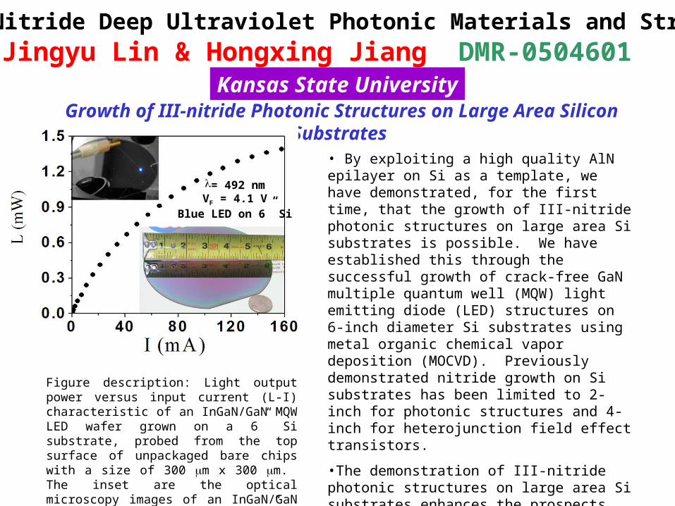
• By exploiting a high quality AlN epilayer on Si as a template, we have demonstrated, for the first time, that the growth of III-nitride photonic structures on large area Si substrates is possible. We have established this through the successful growth of crack-free GaN multiple quantum well (MQW) light emitting diode (LED) structures on 6-inch diameter Si substrates using metal organic chemical vapor deposition (MOCVD). Previously demonstrated nitride growth on Si substrates has been limited to 2-inch for photonic structures and 4-inch for heterojunction field effect transistors.
•The demonstration of III-nitride photonic structures on large area Si substrates enhances the prospects for achieving photonic integrated circuits (PICs) based upon III-nitrides on Si - a material system that is compatible with the standard processes for making silicon computer chips (or CMOS technology).
Figure description: Light output power versus input current (L-I) characteristic of an InGaN/GaN MQW LED wafer grown on a 6” Si substrate, probed from the top surface of unpackaged bare chips with a size of 300 m x 300 m. The inset are the optical microscopy images of an InGaN/GaN MQW blue LED wafer grown on 6” Si substrate.
= 492 nmVF = 4.1 V
Blue LED on 6” Si

Kansas State University
III-Nitride Deep Ultraviolet Photonic Materials and Structures Jingyu Lin & Hongxing Jiang DMR-0504601
Growth of III-nitride Photonic Structures on Large Area Silicon Substrates
500 m500 m
Figure description: Schematics of of InGaN/GaN MQW LED structures grown on 6” Si substrates (a) without the use of AlN epilayer template (cracks are visible). (b) with the use of AlN epilayer template (cracks are completely eliminated).
(a) (b) • It is well known that the large lattice and coefficient of thermal expansion mismatches between Si and GaN makes it highly challenging to grow nitride epilayers on Si substrates with high quality. Apart from a high dislocation density in the grown nitride films due to the large lattice mismatch, another main challenge is managing the stress induced by the coefficient of thermal expansion mismatch that leads to cracks in epilayers thicker than 1 m. For the growth of nitride materials on large area Si substrates, problems associated with cracks and bowing can be more severe because of the increased difficulty of maintaining temperature uniformity and mechanical strength over a larger area.
• The relatively small lattice constant of an AlN epilayer, however, has the potential to counterbalance the thermally induced tensile strains by inducing compressive strain on the subsequent GaN layers, thereby supporting the growth of crack-free and relatively thick GaN layers. We have exploited this potential to fabricate crack-free 492-nm blue LEDs on 6-inch Si substrates with a total thickness exceeding 3 m with high performance.

Kansas State University
III-Nitride Deep Ultraviolet Photonic Materials and Structures Jingyu Lin & Hongxing Jiang DMR-0504601
Growth of III-nitride Photonic Structures on Large Area Silicon Substrates
The P.I. (Lin) of this project serves as a faculty advisor for the Woman in Engineering and Science Program (WESP) at Kansas State University. The program provides outreach, recruitment, and programs for girls and women from middle school through post-graduate levels, to encourage them to consider and persist in careers in science, mathematics and engineering. Prof. Lin conducts demonstrations on LEDs, lasers and optical effects in local schools several times a year in order to reach out to the broader community. The PI’s lab is a “hot” spot for illustrating “Science in Action” to local students. She also participates in a yearly university open-house demonstrating progress in III-nitride photonic devices through NSF supported materials research.
Reaching out to local school girls
Figure description: Prof. Lin hosts students visiting from local middle schools and puts them to work in her lab.