studentsrepo.um.edu.mystudentsrepo.um.edu.my/4234/1/thesis-_final.pdf · abstract ii abstract this...
TRANSCRIPT
INFLUENCE OF HYDROGENATED AMORPHOUS CARBON
UNDERLAYER FILM ON THE FORMATION OF
CARBON NITRIDE NANOSTRUCTURES
NOOR HAMIZAH BINTI KHANIS
DISSERTATION SUBMITTED IN FULFILLMENT OF
THE REQUIREMENTS FOR THE DEGREE OF
MASTER OF SCIENCE
DEPARTMENT OF PHYSICS
FACULTY OF SCIENCE
UNIVERSITY OF MALAYA
KUALA LUMPUR
2013

UNIVERSITI MALAYA
ORIGINAL LITERARY WORK DECLARATION
Name of Candidate: NOOR HAMIZAH BINTI KHANIS (I.C/Passport No: 860104-085206)
Registration/Matric No: SGR090097
Name of Degree: MASTER OF SCIENCE (DISSERTATION)
Title of Project Paper/Research Report/Dissertation/Thesis (“this Work”):
INFLUENCE OF HYDROGENATED AMORPHOUS CARBON UNDERLAYER FILM ON
THE FORMATION OF CARBON NITRIDE NANOSTRUCTURES
Field of Study: THIN FILMS
I do solemnly and sincerely declare that:
(1) I am the sole author/writer of this Work; (2) This Work is original; (3) Any use of any work in which copyright exists was done by way of fair dealing and for permitted purposes and any excerpt or extract from, or reference to or reproduction of any copyright work has been disclosed expressly and sufficiently and the title of the Work and its authorship have been acknowledged in this Work; (4) I do not have any actual knowledge nor do I ought reasonably to know that the making of this work constitutes an infringement of any copyright work; (5) I hereby assign all and every rights in the copyright to this Work to the University of Malaya (“UM”), who henceforth shall be owner of the copyright in this Work and that any reproduction or use in any form or by any means whatsoever is prohibited without the written consent of UM having been first had and obtained; (6) I am fully aware that if in the course of making this Work I have infringed any copyright whether intentionally or otherwise, I may be subject to legal action or any other action as may be determined by UM.
Candidate’s Signature: Date:
Subscribed and solemnly declared before,
Witness’s Signature: Date:
Name:
Designation:
Abstract
ii
Abstract
This study is focused on the effects of the structural properties of the
hydrogenated amorphous carbon (a-C:H) underlayer on the subsequent formation of
carbon nitride nanostructures (ns-CNx). Both layers were prepared sequentially using
radio-frequency plasma enhanced chemical vapour deposition (RFPECVD). The a-C:H
underlayers and ns-CNx were deposited from pure methane and a mixture of pure
methane and nitrogen gases, respectively. The deposition parameters of the ns-CNx
were fixed while the parameters relating to the deposition of a-C:H underlayers were
varied. Three sets of ns-CNx deposited using fixed deposition parameters on a-C:H
underlayer were studied. The first two sets of ns-CNx samples were deposited on a-C:H
underlayers grown at different deposition time duration and RF power. The H2 plasma
treatment time duration done on a-C:H underlayers were varied for the third set of
ns-CNx samples. The structural properties of the a-C:H underlayers studied were
characterized using atomic force microscopy (AFM), Fourier transform infrared
spectroscopy (FTIR) and Raman spectroscopy while the structural properties of ns-CNx
samples were characterized using field emission scanning electron microscopy
(FESEM), FTIR spectroscopy, Raman spectroscopy and Auger electron spectroscopy.
It was determined that the a-C:H underlayer with highest surface roughness of
6 nm results in the formation of rigid vertically aligned CNx nanorods. The a-C:H
underlayer with highest surface roughness which induced the formation of cone-like
structures was shown to have an ordered structure of sp2 clusters and the optimized
deposition time duration for the growth of the underlayer was established to be 10
minutes. By varying the applied RF power at 30-80 W, ion bombardment was shown to
play an important role in changing the surface morphology of a-C:H underlayer. From
the FTIR analysis, the a-C:H underlayer with highest surface roughness shows low CHn
band associated with low H content, and dominant sp2 clustering. These properties
induced the formation of the said rigid vertically aligned CNx nanorods. It was also
found that by tuning the RF power, unique flower-like ns-CNx structure was formed.
The treatment of H2 plasma at different time at 3, 5 and 10 minutes on these a-C:H
underlayers showed that H bombardment could be used effectively to modify the
surface morphology of the underlayer films. In contrast to the high surface roughness
requirement for the growth of nanorods, CNx nanotips were formed on smooth a-C:H
underlayer film surface.
These results showed the effects of changes in structural properties of a-C:H
underlayers on the formation of different ns-CNx. The ns-CNx formed were rigid
vertically aligned nanorods, nanotip and the rare flower-like structures. Both layers
were able to be fabricated in the same system at low deposition temperature of 100 oC
without the use of catalyst. High N content and preferential formation of -N≡C bonds
are crucial aspects in the formation of rigid and vertically aligned nanorods.
Abstrak
iii
Abstrak
Kajian ini ditumpukan kepada kesan sifat struktur filem nipis amorfus karbon
berhidrogen (a-C:H) yang digunakan sebagai substrat dasar bagi pembentukan karbon
nitrida bernanostruktur (ns-CNx). Kedua-dua lapisan ini dihasilkan berturutan
menggunakan pemendapan frekuensi radio wap kimia secara peningkatan plasma
(RFPECVD). Lapisan dasar a-C:H dan berikutnya ns-CNx, masing-masing
dimendapkan daripada metana tulen dan campuran gas metana tulen dan nitrogen.
Parameter bagi pemendapan ns-CNx ditetapkan manakala bagi lapisan a-C:H, parameter
yang digunakan diubah. Tiga set ns-CNx yang dimendapkan menggunakan parameter
pemendapan yang tetap dimendapkan di atas lapisan dasar a-C:H telah dikaji. Dua set
pertama terdiri dari sampel ns-CNx yang dimendapkan di atas lapisan dasar a-C:H yang
dimendapkan pada tempoh masa dan kuasa RF yang berbeza-beza. Lapisan dasar a-C:H
yang dirawat dalam plasma H2 pada tempoh masa berbeza-beza digunakan sebagai
lapisan dasar untuk sampel ns-CNx bagi set ketiga. Sifat struktur bagi lapisan dasar
a-C:H telah dikaji menggunakan mikroskopi daya atom (AFM), spektroskop inframerah
transfomasi Fourier (FTIR) dan spektroskopi Raman manakala sifat struktur bagi
ns-CNx dikaji menggunakan mikroskopi pancaran medan pengimbasan elektron
(FESEM), spektroskopi FTIR dan spektroskopi elektron Auger.
Lapisan dasar yang mempunyai kekasaran permukaan yang paling tinggi iaitu 6
nm menyebabkan pembentukan CNx rod-nano yang tegar dan secara menegak.
Kekasaran permukaan lapisan dasar a-C:H yang tinggi mendorong pembentukan
struktur menyerupai kon yang mengandungi kelompok sp2
yang tertib dan ini
dioptimumkan pada tempoh pemendapan lapisan dasar sebanyak 10 minit. Dengan
mengubah kuasa frekuensi radio (RF) yang dikenakan daripada 30-80 W, hentaman ion
memainkan peranan penting dalam mengubah morfologi permukaan lapisan dasar a-
C:H. Daripada analisis FTIR, lapisan dasar a-C:H yang mempunyai kekasaran paling
tinggi menunjukkan jalur CHn yang rendah yang dikaitkan dengan kandungan H rendah,
dan pengkelompokan sp2. Sifat-sifat yang dominan ini mendorong pembentukan rod-
nano CNx yang tegar dan menjajar secara menegak. Pembentukan struktur unik
menyerupai bunga juga diperolehi dengan mengubah kuasa RF. Rawatan plasma H2
pada 3, 5 dan 10 minit ke atas lapisan dasar a-C:H menunjukkan bahawa hentaman H2
boleh digunakan secara berkesan dalam mengubah morfologi permukaan lapisan filem
dasar. Berbeza dengan rod-nano yang memerlukan permukaan ynag kasar, tip-nano CNx
telah dihasilkan di atas lapisan dasar a-C:H yang rata.
Keputusan ini menunjukkan kesan perubahan dalam sifat struktur lapisan dasar
a-C:H berpotensi terhadap pembentukan ns-CNx yang berbeza. ns-CNx terbentuk adalah
rod-nano yang tegar dan menjajar secara tegak, tip-nano dan struktur menyerupai bunga
yang jarang ditemui. Kedua-dua lapisan boleh disediakan dalam sistem yang sama pada
suhu yang rendah iaitu 100 oC tanpa penggunaan bahan pemangkin. Kandungan N yang
tinggi dan pembentukan -N≡C adalah aspek penting dalam pembentukan rod-nano yang
tegar dan menjajar secara tegak.

Acknowledgement
iv
Acknowledgment
In the name of Allah, Most Gracious, Most Merciful.
All Praise to Allah for His blessing and strength to make completion of this
dissertation a reality. I would like to express my sincere gratitude to my supervisor,
Associate Professor Dr. Siti Meriam Ab. Gani for valuable guidance and endless
support throughout my MSc work. Not forgotten are all the lecturers of Low
Dimensional Materials Research Centre, especially to Professor Datin Dr. Saadah Abd.
Rahman for her constructive advice and guidance. I would also like to thank the science
officer, Pn. Zurina Marzuki, the assistant science officers Pn. Norlela Mohamed
Shahardin and En. Mohamad Aruf; and all members of the Physics Department for their
kindness.
Million thanks to Dr. Richard Ritikos for endless guidance, supportive comment
and encouragement during my MSc work. I would like to express my appreciation to
my colleagues Ms. Maisara Othman and Ms. Nur Maisarah Abdul Rashid for being kind
and supportive and going through this hardship together. My gratitude also goes to Siti
Hajar, Nor Khairiah, Mohd. Ragib, Chong Su Kong, Chan Kee Wah, Dr Goh Boon
Tong and all the members of Low Dimensional Materials Research Centre.
I would like to thank University of Malaya for SBUM scholarship scheme to
support my MSc. I would also like to acknowledge the financial support given,
including University Research Grant RG064-09AFR, Fundamental Research Grants
FP016/2008C and FP052/2010B and short term grant PS308/2009C.
Last but not least, my deepest gratitude to my families (in-laws included)
especially to my beloved parents Tn. Hj. Khanis Khayon and Pn. Hjh. Homsinah
Mohamad for the love, support and endless prayers. My gratitude also goes to my
sibling Noor Rashidah and Nadzri Amini. My special thanks also to my beloved
husband, Fakrul Hakimi Osman for his understanding, care and love.
To those who indirectly contribute to this work, your kindness means a lot to
me.
Thank you.
Table of Content
v
Table of Content
Abstract…………………………………………………………………………....... ii
Abstrak……………………………………………………………………………… iii
Acknowledgment…………………………………………………………………… iv
Table of Content……………………………………………………………………. v
LIST OF FIGURES………………………………………………………………… ix
LIST OF TABLES…………………………………………………………………. xiv
LIST OF PUBLICATIONS……………………………………………………….. xv
LIST OF ABBREVIATIONS……………………………………………………… xvi
CHAPTER 1: INTRODUCTION………………………………………………... 1
1.1 Development on Carbon Nitride………………………….……………….. 1
1.2 Properties of Carbon Nitride and Application…………………………… 3
1.3 Related Works, Motivation and Objectives for This Study……………… 4
1.4 Thesis Outline………………………………………………………………. 6
CHAPTER 2: LITERATURE REVIEW………………………………………. 8
2.1 Introduction………………………………………………………………… 8
2.2 Carbon Nitride Nanostructures…………………………………………… 8
2.2.1 Nanorods…………………………………………………………….. 8
2.2.2 Nanotubes…………………………………………………………… 9
2.2.3 Nanotips……………………………………………………………… 10
2.2.4 Other ns-CNx………………………………………………………… 11
2.3 Review on Preparation of Carbon Nitride Nanostructures……………... 15
2.3.1 Sputtering…………………………………………………………….. 16
2.3.2 Arc Discharge……………………………………………………….. 17
Table of Content
vi
2.3.3 Laser Ablation……………………………………………………….. 18
2.3.4 Chemical Vapour Deposition………………………………………... 19
2.3.4.1 Hot filament plasma enhanced CVD………………………… 19
2.3.4.2 Electron cyclotron resonance CVD………………………….. 20
2.3.4.3 Radio frequency plasma enhanced CVD……………………. 21
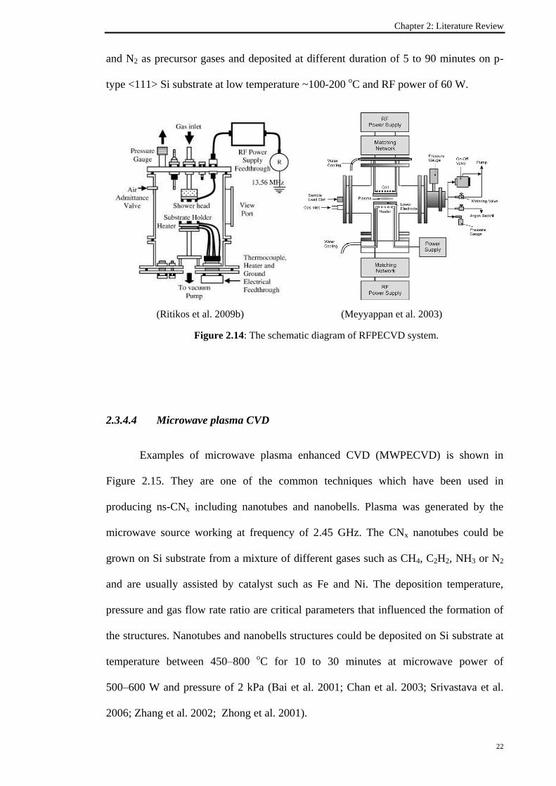
2.3.4.4 Microwave plasma CVD…………………………………….. 22
2.3.4.5 Floating catalyst CVD……………………………………….. 23
2.4 Substrate Condition………………………………………………………… 24
2.4.1 Bare Substrate………………………………………………………... 24
2.4.2 Catalyst………………………………………………………………. 25
2.4.3 Template and Underlayer……………………………………………. 26
2.5 Review of Analytical Methods……………………………………………... 27
2.5.1 Fourier Transform Infrared Spectroscopy…………………………… 27
2.5.2 Raman Spectroscopy………………………………………………… 31
CHAPTER 3: EXPERIMENTAL AND ANALYTICAL TECHNIQUES……. 34
3.1 Introduction……………………………………………………………….... 34
3.2 Radio Frequency Plasma Enhanced Chemical Vapour Deposition
System………………………………………………………………………. 34
3.3 Sample Preparation........................................................................................ 38
3.3.1 Substrate Cleaning Procedures………………………………………. 38
3.3.2 Pre-deposition Process………………………………………………. 38
3.3.3 Deposition Process…………………………………………………... 40
3.3.4 Post-deposition Process……………………………………………… 44
3.4 Analytical Technique……………………………………………………….. 44
3.4.1 Atomic Force Microscopy…………………………………………… 44
3.4.2 Profilometer………………………………………………………….. 47
3.4.3 Scanning Electron Microscopy……………………………………… 48
Table of Content
vii
3.4.4 Fourier Transmission Infrared Spectroscopy Measurement………… 50
3.4.5 Raman Spectroscopy………………………………………………… 56
3.4.6 Auger Electron Spectroscopy………………………………………... 58
CHAPTER 4: EFFECTS OF HYDROGENATED AMORPHOUS CARBON
UNDERLAYER ON THE FORMATION OF CARBON NITRIDE
NANOSTRUCTURES: RESULTS, ANALYSIS AND DISCUSSION………….. 61
4.1 Introduction………………………………………………………………… 61
4.2 Effects of Deposition Time Duration of a-C:H Underlayer and
Resulting CNx/ a-C:H Formation………………………………………….. 64
4.2.1 Effects of Deposition Time Duration on a-C:H Underlayers………... 64
4.2.1.1 Growth rate of a-C:H underlayers…………………………… 64
4.2.1.2 Surface roughness and surface morphology of a-C:H
underlayers…………………………………………………… 66
4.2.1.3 Chemical bonding properties of a-C:H underlayers…………. 68
4.2.1.4 Raman Analysis……………………………………………… 72
4.2.2 Effect on Resulting ns-CNx/a-C:H Formation……………………….. 76
4.2.2.1 Surface and cross-sectional images………………………….. 76
4.2.2.2 Auger electron spectroscopy measurement of ns-CNx………. 79
4.2.2.3 FTIR spectra of ns-CNx……………………………………… 80
4.2.3 Summary……………………………………………………………... 85
4.3 Effects of RF Power on a-C:H Underlayer and Resulting CNx/a-C:H
Formation…………………………………………………………………… 86
4.3.1 Effects of RF Power on a-C:H Underlayer…………………………... 86
4.3.1.1 Growth rate of a-C:H underlayers…………………………… 86
4.3.1.2 Surface roughness and surface morphology of a-C:H
underlayers……………………………………………………
87
4.3.1.3 FTIR spectra of a-C:H underlayers………………………….. 90
4.3.1.4 Raman scattering analysis…………………………………… 92
4.3.2 Effect of RF Power on Resulting CNx/a-C:H Formation……………. 97
4.3.2.1 Surface and cross-sectional images………………………….. 97
Table of Content
viii
4.3.2.2 Auger electron spectroscopy measurement of CNx
nanostructures………………………………………………... 100
4.3.2.3 FTIR spectra of CNx nanostructures…………………………. 102
4.3.3 Summary…………………………………………………………….. 107
4.4 Effects of Hydrogen Treatment on the a-C:H Underlayer and the
Resulting CNx/ a-C:H Film………………………………………………… 108
4.4.1 Effect of H2 Treatment Time Duration on a-C:H Underlayers……… 109
4.4.1.1 Surface roughness and surface morphology of a-C:H
underlayers…………………………………………………… 109
4.4.1.2 Chemical bonding properties of a-C:H underlayers…………. 111
4.4.1.3 Raman analysis 114
4.4.2 Effect on Resulting CNx/a-C:H Formation…………………………... 119
4.4.2.1 Surface and cross-sectional images………………………….. 119
4.4.2.2 Auger electron spectroscopy measurement of ns-CNx………. 121
4.4.2.3 FTIR spectra of ns-CNx……………………………………… 122
4.4.3 Summary……………………………………………………………... 127
CHAPTER 5: CONCLUSION AND FUTURE WORKS……………………… 129
5.1 Conclusion…………………………………………………………………... 129
5.2 Future Works……………………………………………………………….. 131
REFERENCES……………………………………………………………………… 132
List of Figures
ix
LIST OF FIGURES
Figure 1.1: Progression chart of ns-CNx. 2
Figure 2.1: Example of FESEM images CNx nanorods. 9
Figure 2.2: Example SEM images of various CNx nanotubes structure. 10
Figure 2.3: FESEM images of CNx nanotips. 11
Figure 2.4: HRTEM image of CNx nanobell. 12
Figure 2.5: SEM images of carbon nitride (a) aligned nanoribbons and (b)
microsphere nanoribbons.
13
Figure 2.6: TEM image of the CNx nanospheres. 13
Figure 2.7: SEM image the formation of (a) nano-petals and (b) flower-like
CNx structure.
14
Figure 2.8: The TEM image of CNx leaf-like structures. 15
Figure 2.9: The example of schematic diagram of magnetron sputtering system. 16
Figure 2.10: Example of schematic diagram of arc discharge system. 17
Figure 2.11: Example of schematic diagram of pulsed laser ablation system. 18
Figure 2.12: Example of schematic diagram of HFPECVD system. 20
Figure 2.13: The example of schematic diagram ECRCVD system. 21
Figure 2.14: The schematic diagram of RFPECVD system. 22
Figure 2.15: Example of schematic diagram of MWPECVD system. 23
Figure 2.16: Example of typical schematic diagram of floating catalyst CVD
system.
24
Figure 2.17: The example of template used in CNx nanotubes fabrication. 26
Figure 2.18: Type of vibration mode in FTIR analysis. 28
Figure 2.19: Example of typical FTIR spectra of a-C:H film. 29
Figure 2.20: Example of typical FTIR spectra of CNx film. 29
Figure 2.21: Typical Raman spectra for carbon based materials. 32
Figure 3.1: Schematic diagram of RFPECVD system. 35

List of Figures
x
Figure 3.2: Schematic diagram of RFPECVD system reaction chamber. 37
Figure 3.3: Top view mask of substrate holder. 39
Figure 3.4: Single a-C:H underlayer deposited on Si substrate and CNx film
deposited on a-C:H underlayer prepared by RFPECVD.
40
Figure 3.5: Chart of sample preparation. 42
Figure 3.6: Plasma discharge during deposition process. 43
Figure 3.7: Schematic diagram of AFM. 45
Figure 3.8: VEECO Dimension 3000 atomic force microscope. 45
Figure 3.9: Surface morphological (a) and roughness analysis (b) of a-C:H
underlayer deposited by RFPECVD at 10 minutes.
46
Figure 3.10: KLA TENCO P-6 profilometer. 47
Figure 3.11: Data observed from profilometer for film deposited at 100 W RF
power with 3 minutes hydrogen treatment process.
48
Figure 3.12: FEI Quanta 200 field emission scanning electron microscope. 49
Figure 3.13: Surface (a) and cross section (b) images of CNx film deposited on
a-C:H underlayer prepared at RF power of 50 W.
50
Figure 3.14: Schematic diagram of Fourier Transform Infrared Spectrometer. 51
Figure 3.15: The Perkin Elmer System 2000 FTIR spectrometer. 52
Figure 3.16: FTIR spectrum of a-C:H underlayer. 53
Figure 3.17: FTIR spectrum of CNx nanostructures. 53
Figure 3.18: Example of deconvolution FTIR absorption peaks of a-C:H
underlayer and CNx nanostructures in wavenumber region of 2000-2300 cm-1
.
55
Figure 3.19: The Renishaw inVia Raman Microscope. 56
Figure 3.20: Raman spectra with the baseline (a) and corrected Raman spectra
with the Gaussian fitting D and G bands (b)
57
Figure 3.21: Schematic diagram of Auger electron process. 58
Figure 3.22: JAMP-9500F Field Emission Auger Microprobe. 60
Figure 3.23: AES spectra variation of CNx prepared on different deposition
duration of a-C:H underlayer and bare c-Si substrate.
60

List of Figures
xi
Figure 4.1: Summary of the methodology and variations in film preparation
parameters
63
Figure 4.2: Thickness (■) and growth rate (♦) of a-C:H underlayer deposited by
RFPECVD for different deposition time duration. The line is only an eye-
guide.
65
Figure 4.3: AFM surface morphology of (a) bare c-Si, a-C:H underlayers
deposited for tD of (b) 5, (c)10, (d) 15 and (e) 30 minutes.
66
Figure 4.4: Variation of surface roughness of bare c-Si and a-C:H underlayers
deposited at 5, 10, 15 and 30 minutes.
67
Figure 4.5: The FTIR spectra of a-C:H underlayer deposited for varied
deposition duration.
68
Figure 4.6: Variation of FTIR spectra for a-C:H underlayers deposited at
different duration of 5, 10, 15 and 30 minutes.
71
Figure 4.7: The raw Raman spectra with strong background (a) and the Raman
spectra after the background extraction (b) for a-C:H underlayers prepared at
different deposition duration of 5, 10, 15 and 30 min.
73
Figure 4.8: Raman analysis of a-C:H underlayers prepared at tD of 5, 10, 15 and
30 minutes. Line is guide to the eyes.
75
Figure 4.9: Surface and cross-sectional images of ns- CNx deposited on a-C:H
underlayer prepared at different tD.
76
Figure 4.10: Variation of FESEM cross-sectional images for ns-CNx deposited
on bare c-Si and 10 minutes a-C:H underlayer.
78
Figure 4.11: Variation of nitrogen to carbon N/C ratio of ns-CNx deposited on
c-Si, a-C:H underlayers at tD of 5, 10, 15 and 30 minutes.
79
Figure 4.12: Variation in FTIR absorbance spectra of ns-CNx as a function of
deposition duration of a-C:H underlayers.
81
Figure 4.13: The FTIR spectra for ns-CNx deposited at different tD of a-C:H
underlayers in the range of (a) sp2, (b) sp
1 and(c) sp
3 phases.
82
Figure 4.14: The FTIR spectra in the wavenumber range of 1900-2300 cm-1
of
CNx nanostructres as a function of tD a-C:H underlayers.
83
Figure 4.15: Gaussian fitting profiles for FTIR spectra in wavenumber region
of 2000-2300 cm-1
for a-C:H underlayer at tD 10, 30 minutes and c-Si.
84
Figure 4.16: Growth rate of a-C:H underlayers deposited by RFPECVD at
different RF power. The line is only an eye-guide.
87

List of Figures
xii
Figure 4.17: AFM surface morphology of a-C:H underlayers deposited for RF
power of 30, 40, 50, 60, 80 and 100 W.
88
Figure 4.18: Variation of surface roughness of a-C:H underlayers deposited at
RF power of 30, 40, 50, 60, 80 and 100 W.
89
Figure 4.19: The FTIR spectra of a-C:H underlayer at different RF power of
30, 40, 50, 60, 80 and 100 W.
91
Figure 4.20: Variation of FTIR spectra for a-C:H underlayers deposited at
different RF power in the range of 1400-2000 cm-1
and 2600-4000 cm-1
.
92
Figure 4.21: Raw Raman spectra (a) and corrected Raman spectra (b) of a-C:H
underlayers as a function of RF power.
94
Figure 4.22: Raman analysis of a-C:H underlayers prepared at different RF
power.
96
Figure 4.23: Surface and cross-section images of ns:CNx deposited by
RFPECVD at different RF power of a-C:H underlayer.
98
Figure 4.24: FESEM cross section image for ns-CNx deposited on pre-
deposited a-C:H underlayer with surface roughness of 5.956.
100
Figure 4.25: FESEM surface image for ns-CNx deposited on pre-deposited
a-C:H underlayer with surface roughness of 2.783.
100
Figure 4.26: Variation of nitrogen to carbon N/C ratio of ns-CNx films as a
function of surface roughness of a-C:H underlayers.
101
Figure 4.27: Variation in FTIR absorbance spectra as a function surface
roughness of a-C:H underlayers.
103
Figure 4.28: The FTIR spectra for CNx nanostructures deposited on a-C:H
underlayers with different roughness in the range of (a) sp2, (b) sp
1 and (c) sp
3
phases.
104
Figure 4.29: The FTIR spectra in the range of 1900-2300 cm-1
of ns-CNx as a
function of RUL a-C:H underlayers.
106
Figure 4.30: Gaussian fitting profiles for FTIR spectra in the region
2000-2300 cm-1
for a-C:H underlayers with surface roughness 5.596 and 3.262.
107
Figure 4.31: AFM surface morphology of a-C:H underlayers at various time
duration of H2 plasma treatment.
109
Figure 4.32: Variation of surface roughness of a-C:H underlayer as a function
of tH. Line is a guide to the eyes.
110
Figure 4.33: FTIR spectra of a-C:H underlayers as a function of tH. 112

List of Figures
xiii
Figure 4.34: Variation of FTIR spectra for a-C:H underlayers prepared by
RFPECVD as a function of tH in regions of (a) 1300-1900 cm-1
and (b)
2700-3200 cm-1
.
113
Figure 4.35: The raw Raman spectra with strong background (a) and the Raman
spectra after the background extraction (b) for a-C:H underlayers as a function
of tH.
117
Figure 4.36: Raman analysis of a-C:H underlayers prepared as a function
hydrogen treatment duration. Line is guide to the eyes.
118
Figure 4.37: The surface and cross-section images of ns-CNx subsequently
deposited on different tH a-C:H underlayers.
120
Figure 4.38: Variation of nitrogen to carbon, N/C ratio of ns-CNx deposited on
different tH a-C:H underlayers.
122
Figure 4.39: Variation in FTIR absorbance spectra of ns-CNx as a function of
H2 treatment time of a-C:H underlayers.
123
Figure 4.40: The FTIR spectra for ns-CNx deposited on different tH of a-C:H
underlayers in the range of (a) sp2, (b) sp
1 and (c) sp
3 phases.
124
Figure 4.41: The FTIR spectra in the wavenumber range of 1900-2300 cm-1
of
ns-CNx as a function of tH a-C:H underlayers.
125
Figure 4.42: Gaussian fitting profiles for FTIR spectra in wavenumber region
of 1900-2400 cm-1
for a-C:H underlayer at tH of 3, 5, 10 minutes and a-C:H
underlayer without H2 treatment.
127

List of Tables
xiv
LIST OF TABLES
Table 2.1: The assignments FTIR vibrational frequencies of a-C:H underlayer and
nanostructured CNx films prepared by RFPECVD…………………………….……....30
Table 3.1: Deposition parameter of a-C:H layer and CNx nanostructures……..………43
List of Publications
xv
LIST OF PUBLICATIONS
Reviewed paper
1. Effect of pre-deposited carbon layer on the formation of carbon nitride
nanostructures prepared by radio-frequency plasma enhanced chemical vapour
deposition.
Materials Chemistry and Physics 130 (2011) 218–222
Noor Hamizah Khanis, Richard Ritikos, Maisara Othman, Nur Maisarah Abdul Rashid,
Siti Meriam Ab Gani, Muhamad Rasat Muhamad, Saadah Abdul Rahman
Impact factor: 2.353 Category: Q1
2. Catalyst free carbon nitride nanostructures prepared by rf-pecvd technique on
hydrogenated amorphous carbon template.
Materials Chemistry and Physics
Noor Hamizah Khanis, Richard Ritikos, Maisara Othman, Nur Maisarah Abdul Rashid,
Siti Meriam Ab. Gani and Saadah Abdul Rahman
Impact factor: 2.353 Category: Q1
Other related papers
1. Effect of N2 flow rate on the properties of CNx thin films prepared by radio
frequency plasma enhanced chemical vapor deposition from ethane and nitrogen.
Thin Solid Films (2012)
Maisara Othman, Richard Ritikos, Noor Hamizah Khanis, Nur Maisarah Abdul Rashid,
Siti Meriam Ab Gani, Saadah Abdul Rahman
Impact factor: 1.909 Category: Q1
2. Effects of rf power on the structural properties of carbon nitride thin films
prepared by plasma enhanced chemical vapour deposition.
Thin Solid Films 519 (2011) 4981–4986
Maisara Othman, Richard Ritikos, Noor Hamizah Khanis, Nur Maisarah Abdul Rashid,
Saadah Abdul Rahman, Siti Meriam Ab Gani, Muhamad Rasat Muhamad
Impact factor: 1.909 Category: Q1

List of Abbreviations
xvi
LIST OF ABBREVIATIONS
a-C:H Hydrogenated amorphous carbon
CH4 Methane
CNx Carbon nitride
DC Direct current
FWHM Full width half maximum
H2 Hydrogen
MFC Mass flow controller
N2 Nitrogen
ns-CNx Carbon nitride nanostructures
PUL Power of underlayer
RF Radio frequency
RFPECVD Radio frequency plasma enhanced chemical vapour deposition
RUL Surface roughness of underlayer
sccm Standard cubic centimeter per minute
Si Silicon
tD Deposition time duration
tH Hydrogen treatment time duration
Chapter 1: Introduction
1
CHAPTER 1 : INTRODUCTION
1.1 Development on Carbon Nitride
Studies on carbon nitride (CNx) films have received considerable attention in
recent years particularly after 1979 following the work by Cuomo et al. In their work,
CNx films were prepared by reactive RF sputtering of carbon in nitrogen (Cuomo et al.
1979). The interest on CNx films further expanded following the work done by Liu and
Cohen in 1989 which reported the feasibility of producing β-C3N4 which is analogous to
β-Si3N4 having hardness comparable to diamond (Liu and Cohen 1989). Over the years,
the research continues with the discovery of various types of CNx structures including
diamond, graphitic, polymeric and others (Shimoyama et al. 2001; Sung and Sung
1996; Zambov et al. 2000).
Fabrication of one dimensional CNx nanostructures is one of the most significant
progress in the study of carbon related films beginning with the work carried out by
Pradeep et al. in incorporating N in fullerene in 1991. This was followed by various
work to fabricate other CNx nanostructures (ns-CNx) such as nanotube, nanofiber,
nanorod, nanowire, nanotip, nanosphere, nanoribbon, nanobell and several rare species
including flower-like, leaf-like and worm-like structures (Droppa et al. 2002; Pradeep et
al. 1991; Wang and Ostrikov 2009; Yang, et al. 2006). The most recent progression in
the fabrication of ns-CNx focused on incorporating nitrogen into single or multilayer
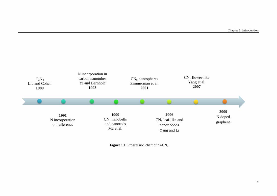
graphene sheets (Qu et al. 2010; Shao et al. 2010; Wang et al. 2010). Figure 1.1
summarizes the progression of the works done on ns-CNx.
Chapter 1: Introduction
2
CNx flower-like
Yang et al.
2007
CNx nanospheres
Zimmerman et al.
2001
C3N4
Liu and Cohen
1989
N incorporation in
carbon nanotubes
Yi and Bernholc
1993
2009
N doped
graphene
2006
CNx leaf-like and
nanoribbons
Yang and Li
1999
CNx nanobells
and nanorods
Ma et al.
1991
N incorporation
on fullerenes
Figure 1.1: Progression chart of ns-CNx.

Chapter 1: Introduction
3
1.2 Properties of Carbon Nitride and Application
CNx is a promising material in various applications due to its interesting and
unique properties. Nitrogen incorporation in carbon films leads to structural
transformation with preference to bond as sp2 bonded CNx. In a study reported by Hu et
al. on the preparation of carbon nitride films using plasma-assisted pulsed laser
deposition technique having N incorporation increasing from 12% to 17% results in a
decrease in sp3 bonded carbon from 70% to almost 0% (Hu et al. 1998). Consequently,
sp2 content in the film increased. The increase in N content are caused by the preference
in N to bond to carbon atoms in the films due to the strong electronegativity of N atom.
Additionally, the N atom could be substituted in the carbon network to form double or
single bond subjected to the N concentration (Wang et al. 2008).
N incorporation into carbon films brings about an enhancement in mechanical
characteristic leading to excellent adhesion properties of these films (Lowther 1998;
Ren et al. 1995). Additionally N incorporation also improve the local density of states
near the Fermi level of these materials thus enhances their electronic characteristic.
Such materials are suitable candidates for field emission devices which would show low
turn-on voltage (Chan et al. 2003; Kim et al. 2011; Zhong et al. 2001). Lately, CNx has
gained considerable attention in its potential in various electrical devices, photo-
catalyst, oxygen reduction agent, hydrogen storage material and active sensors (Bai
et al. 2001; Jun et al. 1998; Pan et al. 2011a). One of the outstanding examples is that
reported by Gong et al. on vertically aligned nitrogen containing carbon nanotube used
as metal-free electrode in oxygen reduction reaction to improve fuel cell performance.
These nitrogen containing carbon nanotubes are said to have better characteristic
compared to conventional platinum electrode due to enhancement in electro-catalytic
activity, being more stable for long term operation and at lower production cost
(Gong et al. 2009). Integrated sensor systems including humidity sensitive field effect
Chapter 1: Introduction
4
transistor, temperature sensor and operational amplifier have utilized ns-CNx as a
component material in the device system. This ns-CNx sensor was fabricated by analog
mixed CMOS process (Lee et al. 2008). Other notable example of CNx application is as
hydrogen storage material. This study was done by Ito et al. using amorphous CNx. The
maximum hydrogen content uptake was reported as high as 0.78 wt% which is
dependent on the type of hydrocarbon precursor used for the deposition such as CH4,
C2H6, C2H4 and C6H6 (Ito et al. 2008; Koh et al. 2012).
1.3 Related Works, Motivation and Objectives for This Study
A novel technique of growing vertically aligned CNx nanorods was established
and reported by Ritikos et. al. from Low Dimensional Materials Research Centre,
University of Malaya where this work was carried out (Ritikos et al. 2011). This
technique established the fabrication of CNx nanorods by RF-PECVD at low
temperature (100 oC) using a parallel plate configuration without the use of metal
catalyst. The effect of high electric field induced by small electrode spacing between the
powered electrode and the substrate holder resulted in the formation of these nanorods
at fixed RF power of 80 W in a mixture of methane and nitrogen flow rates of 20 and
47 sccm, respectively. The work also shows that N incorporation is one of the crucial
aspects in obtaining the vertical alignment. However, further work is proposed by that
study to find ways of modifying these structures while retaining a large part of its
deposition parameters and avoiding the use of metal catalysts. The use of catalytic
materials can change the structure of CNx but this sacrifices the purity of the resulting
product since they introduce contaminants into the material structure. Thus, this work
was motivated by these suggestions and also by the emergence of a recent study on the
use of pre-deposited hydrogenated amorphous carbon (a-C:H) underlayer films as
Chapter 1: Introduction
5
template or seeding layer for the growth of carbon nanostructures (Wang et al. 2012b;
Wang and Zhang 2006). These underlayer films would act as the substrate upon which
this nanostructures are built on. Indeed substrate conditioning has been suggested as an
important aspect that can influence the properties of the resulting upper-structures.
Several studies have been carried out on the effects of substrate characteristic including
variations in temperature, crystallinity orientation, morphology, type, and treatment
process (Cao et al. 2007; Gielen et al. 1997; Jayatissa et al. 1998; Sakata et al. 2010;
Smietana et al.2010).
In this work the ns-CNx were deposited on a-C:H underlayers by RF-PECVD.
The ns-CNx were deposited from a mixture of methane and nitrogen at fixed deposition
preparation conditions while methane was used as gas source for the growth of a-C:H
underlayers prepared by varying a specific deposition parameter for each set of
samples. The objectives of this work are as listed below:
(1) To grow the ns-CNx on a-C:H underlayers deposited under these conditions;
i. Different deposition time duration
ii. Different RF powers applied during deposition
iii. Different time duration of H2 plasma treatment
(2) To study the effects of structural properties of a-C:H underlayer on the
morphology of the ns-CNx formed.
Chapter 1: Introduction
6
1.4 Thesis Outline
This Chapter 1 features an introduction to this study and is followed by
Chapter 2 which presents the literature review related to this work. The literature review
is divided into four parts. The first part introduces various types of one-dimensional
ns-CNx including nanorod, nanotube, nanotip and also rare species such as nanobell,
flower-like and leaf-like CNx. The second part covers common deposition techniques
employed to fabricate ns-CNx. The third part looks into various types of substrate
conditioning including film deposition on bare Si substrate, with catalytic assistance or
with template assistance. The last part presents a brief theoretical background on the
two analytical techniques used in this work that is Raman scattering and Fourier
transform infrared spectroscopy.
Chapter 3 presents details on the experimental and analytical techniques used in
this work. These include the deposition procedures and characterization of the films.
The deposition procedures outline the description of the RFPECVD system, substrate
preparation, film deposition and post deposition procedures. The characterization
methods used comprise of atomic force microscopy (AFM), surface profilometer,
scanning electron microscopy (SEM), Fourier transform infrared (FTIR) spectroscopy,
Raman spectroscopy and Auger electron spectroscopy (AES). These methods are
briefly described in this chapter.
Chapter 4 presents the experimental results, analysis and discussion related to
the study of carbon underlayer films and the subsequent fabrication of ns-CNx. The
focus on this chapter is to study the effect of a-C:H underlayer on formation of ns-CNx.
For the a-C:H underlayers, their growth rate, surface roughness, chemical bonding and
structural properties were studied. Subsequently, ns-CNx were grown directly onto these
a-C:H underlayer films. These ns-CNx/a-C:H films were studied in terms of their

Chapter 1: Introduction
7
surface and cross sectional images, growth rates, elemental composition and bonding
properties.
Chapter 5 presents the general conclusion of this study and also offers
suggestions for future works.

Chapter 2: Literature Review
8
CHAPTER 2 : LITERATURE REVIEW
2.1 Introduction
This chapter presents a literature review of two critical topics related to this
work. The first part comprises a review on various types of one dimensional ns-CNx
which can consist of not only nanorod, nanotube, nanotip but also more rare species
such as nanobells, nanoribbon, nanosphere, flower-like and leaf-like CNx. Then, the
next section looks into a brief theoretical background on two particular analytical
techniques related to this work. These include the Fourier transform infrared and Raman
analysis.
2.2 Carbon Nitride Nanostructures
2.2.1 Nanorods
Nanorods are nanostructures with stick or rod shapes with relatively low aspect
ratio. Several investigations have been done in order to fabricate these structures.
Ritikos and co-wokers have found CNx nanorods deposited by RFPECVD at low
temperature and not assisted by catalyst.The CNx nanorods are have diameter of 20-140
nm, length up to 5 µm with high nitrogen content of 42 at.% (Ritikos, et al. 2011).
Moreover, Cespedes et al. also reported high density of 4 cm2 area CNx nanorods with
diameter 50-200 nm and length 1 µm (Cespedes et al. 2005). CNx nanorods were cited
as one of the potential materials for applications in optic, electronic and optoelectronic
devices (Liu et al. 2002a; 2002b). In another related work, Yang et al. obtained aligned
ultra-fine crystalline CNx nanorods prepared by pulsed laser ablation technique at room

Chapter 2: Literature Review
9
temperature (Yang et al. 2007). Figure 2.1 shows SEM images of examples of CNx
nanorods.
Figure 2.1: Example of FESEM images CNx nanorods.
2.2.2 Nanotubes
Carbon nanotube (CNT) can be categorized either as multi wall or single wall
nanotube. Single wall nanotube exhibit only one graphite layer with hexagonal lattice
that appears wrapped up into a seamless cylinder. Multi wall nanotube form as a group
of single wall nanotube with a mutual centre axis (Tu and Ou-Yang 2002). The
inclusion of other element such as B and N into carbon nanotube network has been
studied and it is expected to enhance their properties. From previous work, it was
reported that doping nitrogen to carbon nanotubes network is expected to enhance its
structural, magnetic and electronic properties and the size of carbon nitrogen atom is
almost the same (Che, Peng, and Wang 2004; Ganesan et al. 2010; Krstić et al. 2007;
Moradian and Azadi 2006). From experiment and simulation, Hu et al. showed that
nitrogen influenced the structural properties of CNx. by which it causes relaxation of sp3
bonded carbon to sp2
bonding (Chan et al. 2004; Hu et al. 1998). The enhancement in
electronic characteristic could be applied as field emitting devices (Chan et al. 2003;
Kim et al. 2011; Zhong et al. 2001). This is due to improvement of local density of
(Ritikos et al. 2011) (Liu et al. 2002a)
Chapter 2: Literature Review
10
states near the Fermi level in CNx thus lowers the field emission threshold voltage
(Srivastava et al. 2006). By functionalizing CNT with different transition metals such as
W, Ti, Cr and Mn, the magnetic moment may be aligned to create either ferro or anti-
ferro magnetic properties between neighboring metal atoms. This functionalized CNT
can be applied in gas and energy storage devices (Pan et al. 2011b). Koh et al. showed
that the graphitic CNx nanotubes is one of the promising material in H2 storage with the
ability to uptake up to 4.66 wt. % hydrogen (Koh et al. 2012). Other applications
include utilizing nitrogen doped carbon nanotubes coated with atomic layer of SnO2 as
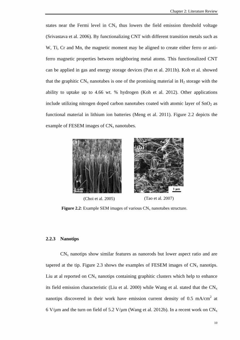
functional material in lithium ion batteries (Meng et al. 2011). Figure 2.2 depicts the
example of FESEM images of CNx nanotubes.
Figure 2.2: Example SEM images of various CNx nanotubes structure.
2.2.3 Nanotips
CNx nanotips show similar features as nanorods but lower aspect ratio and are
tapered at the tip. Figure 2.3 shows the examples of FESEM images of CNx nanotips.
Liu at al reported on CNx nanotips containing graphitic clusters which help to enhance
its field emission characteristic (Liu et al. 2000) while Wang et al. stated that the CNx
nanotips discovered in their work have emission current density of 0.5 mA/cm2 at
6 V/µm and the turn on field of 5.2 V/µm (Wang et al. 2012b). In a recent work on CNx
(Choi et al. 2005) (Tao et al. 2007)
(b)

Chapter 2: Literature Review
11
nanotips prepared by hot filament plasma enhanced CVD system, a thin carbon
underlayer was pre-deposited using RF magnetron sputtering prior to the deposition
procedure. This underlayer was used as seed layer to promote the growth of nanotips. In
another work, Dang and Wang reported on the effect of different growth duration on PL
properties of CNx nanotips. The longer duration resulted in stronger PL intensity due to
strong effect of light trapping within the nanotips. This work showed that the dimension
(length, height and diameter) of the nanotips influences the absorption and reflection
process during the PL measurement (Dang and Wang 2012).
Figure 2.3: FESEM images of CNx nanotips.
2.2.4 Other ns-CNx
Nanobells. Several works have reported the growth of CNx nanobells (Bai et al. 2001;
Wang 2002, 2006; Zhang, et al. 2002). This structure is made up of a series of stacking
graphite cones growing parallel to each other in compartmentalized spaces, were
produced by using microwave plasma enhanced CVD technique from a mixture of CH4
and N2 gases. From the HRTEM image shown in Figure 2.4, these structures were seen
as nanotubes with nanobell compartments where the catalyst are encapsulated at the root
of the fiber like structure. The bell-like structures are made up of a curved top and bend
(Wang et al. 2012a) (Wang and Zhang 2006)
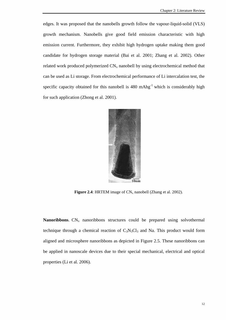
Chapter 2: Literature Review
12
edges. It was proposed that the nanobells growth follow the vapour-liquid-solid (VLS)
growth mechanism. Nanobells give good field emission characteristic with high
emission current. Furthermore, they exhibit high hydrogen uptake making them good
candidate for hydrogen storage material (Bai et al. 2001; Zhang et al. 2002). Other
related work produced polymerized CNx nanobell by using electrochemical method that
can be used as Li storage. From electrochemical performance of Li intercalation test, the
specific capacity obtained for this nanobell is 480 mAhg-1
which is considerably high
for such application (Zhong et al. 2001).
Figure 2.4: HRTEM image of CNx nanobell (Zhang et al. 2002).
Nanoribbons. CNx nanoribbons structures could be prepared using solvothermal
technique through a chemical reaction of C3N3Cl3 and Na. This product would form
aligned and microsphere nanoribbons as depicted in Figure 2.5. These nanoribbons can
be applied in nanoscale devices due to their special mechanical, electrical and optical
properties (Li et al. 2006).

Chapter 2: Literature Review
13
Figure 2.5: SEM images of carbon nitride (a) aligned nanoribbons and
(b) microsphere nanoribbons (Li et al. 2006).
Nanospheres. CNx nanospheres could be prepared using solution reaction or template-
directed solid-state of cynuric chloride or fluoride with lithium nitride. Zimmerman et al
were able to obtain nanosphere with sizes in the range of 30-200 nm. The features of the
nanospheres could be controlled by using silica spheres as template. It is important to
control the sphere size and shape for their application and desired properties
(Zimmerman et al. 2001). Figure 2.6 shows example of TEM image of the CNx
nanospheres.
Figure 2.6: TEM image of the CNx nanospheres (Zimmerman et al. 2001).
(a) (b)

Chapter 2: Literature Review
14
Flower-like. Bai et al. reported the formation of flower-like CNx prepared by the high-
energy ball-milling and subsequent thermal-annealing process in a horizontal tube
furnace using melamine as precursor. In this work, annealing temperature of up to
650oC is the key factor in the successfully formation of flower-like CNx (Bai, Cao and
Xu 2010). Yang et al. fabricated flower-like CNx via liquid pulsed laser ablation
technique using ammonia solution. These structures are made up of self-assembled
nano-petals structures. Different ablation time, laser energy, ammonium concentration
and drying speed play crucial roles in the formation of these flower-like structures.
Figure 2.7 shows examples of SEM images of flower-like CNx (Yang et al. 2007).
Figure 2.7: SEM image the formation of (a) nano-petals
and (b) flower-like CNx structure (Yang et al. 2007).
Leaf-like. Leaf-like CNx structure consists of large number of packed ordered nanorods
could be formed by self-assemble process using liquid phase pulsed laser ablation of
graphite target and ammonia solution. The formation of leaf-like structure depends on
the ablation duration. Such structures have wide band gap and are therefore suitable for
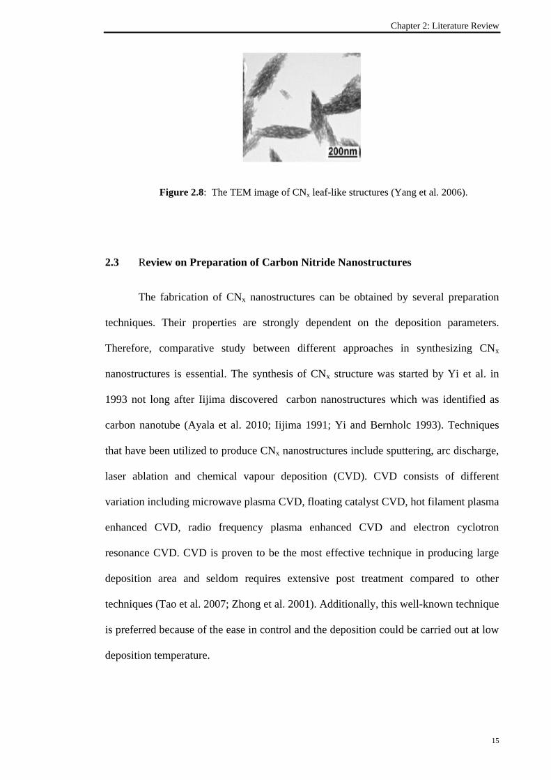
optical application. Example of this structure is shown in Figure 2.8.
(a) (b)
Chapter 2: Literature Review
15
Figure 2.8: The TEM image of CNx leaf-like structures (Yang et al. 2006).
2.3 Review on Preparation of Carbon Nitride Nanostructures
The fabrication of CNx nanostructures can be obtained by several preparation
techniques. Their properties are strongly dependent on the deposition parameters.
Therefore, comparative study between different approaches in synthesizing CNx
nanostructures is essential. The synthesis of CNx structure was started by Yi et al. in
1993 not long after Iijima discovered carbon nanostructures which was identified as
carbon nanotube (Ayala et al. 2010; Iijima 1991; Yi and Bernholc 1993). Techniques
that have been utilized to produce CNx nanostructures include sputtering, arc discharge,
laser ablation and chemical vapour deposition (CVD). CVD consists of different
variation including microwave plasma CVD, floating catalyst CVD, hot filament plasma
enhanced CVD, radio frequency plasma enhanced CVD and electron cyclotron
resonance CVD. CVD is proven to be the most effective technique in producing large
deposition area and seldom requires extensive post treatment compared to other
techniques (Tao et al. 2007; Zhong et al. 2001). Additionally, this well-known technique
is preferred because of the ease in control and the deposition could be carried out at low
deposition temperature.

Chapter 2: Literature Review
16
2.3.1 Sputtering
In sputtering technique, film deposition is carried out by using radio frequency
(RF), direct current (DC) or pulsed DC source as power sources and it generates ions
that can eject material through sputtering process from a target, then deposits the
sputtered elements onto a substrate. CNT coated with amorphous CNx and ns-CNx have
been obtained by RF magnetron sputtering (Banerjee et al. 2010; Kim et al. 2011). The
fabrication process was carried out on c-Si substrate at a working pressure range of
6.7 x 10⁻³
to 5 x 10⁻²
mbar with Ar to N2 flow rate ratio of 1:1 and 4:1, respectively.
High purity graphite was used as target. The deposition was carried out for 3 hours and
10 minutes for CNT coated with amorphous CNx and ns-CNx, respectively. In the
fabrication of the CNT coated with amorphous CNx, Ni with thickness of 7 nm was
used as catalyst. In another study, Suenaga et al. deposited nanotubulite CNx using DC
magnetron sputtering system. The sample was deposited on cleaved NaCl substrate in
Ar/N2. The deposition temperature was at 350 oC (Suenaga et al. 1999). Examples of
conventional sputtering system are shown in Figure 2.9.
Figure 2.9: The example of schematic diagram of magnetron sputtering system.
(Honda et al. 2002) (Iseki 2009)
Chapter 2: Literature Review
17
2.3.2 Arc Discharge
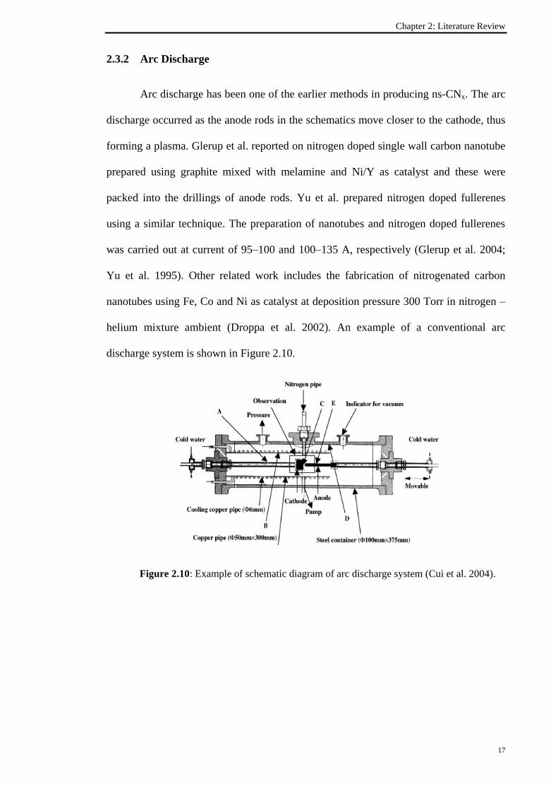
Arc discharge has been one of the earlier methods in producing ns-CNx. The arc
discharge occurred as the anode rods in the schematics move closer to the cathode, thus
forming a plasma. Glerup et al. reported on nitrogen doped single wall carbon nanotube
prepared using graphite mixed with melamine and Ni/Y as catalyst and these were
packed into the drillings of anode rods. Yu et al. prepared nitrogen doped fullerenes
using a similar technique. The preparation of nanotubes and nitrogen doped fullerenes
was carried out at current of 95–100 and 100–135 A, respectively (Glerup et al. 2004;
Yu et al. 1995). Other related work includes the fabrication of nitrogenated carbon
nanotubes using Fe, Co and Ni as catalyst at deposition pressure 300 Torr in nitrogen –
helium mixture ambient (Droppa et al. 2002). An example of a conventional arc
discharge system is shown in Figure 2.10.
Figure 2.10: Example of schematic diagram of arc discharge system (Cui et al. 2004).

Chapter 2: Literature Review
18
2.3.3 Laser Ablation
Laser ablation is one of the common physical vapour deposition used in
producing ns-CNx. Laser ablation occurs when short laser pulses are irradiated onto a
solid or liquid target, which at certain conditions will formed a plasma. The utilization
of laser ablation has a few advantages such as enabling direct chemical analysis for
solids, produces high quality sample with low contamination and enables analysis to be
done without separating the solids and solution. CNx nanorods has been prepared using
a Nd: YAG laser with wavelength of 532 nm focused onto a solid graphite target which
was submerged in a 35% ammonia solution at longer ablation duration of 5 hours.
Alternatively, at lower deposition duration (2 hours), only nanoparticles were formed
(Yang et al. 2007). Other ns-CNx using this technique includes flower-like and leaf-like
CNx which could be produced by controlling the deposition duration (Yang et al. 2007b,
2006a, 2006b). Examples of conventional laser ablation system are shown in
Figure 2.11.
Figure 2.11: Example of schematic diagram of pulsed laser ablation system.
(Sasaki et al. 1998) (Apostol et al. 2011)
Chapter 2: Literature Review
19
2.3.4 Chemical Vapour Deposition
2.3.4.1 Hot filament plasma enhanced CVD
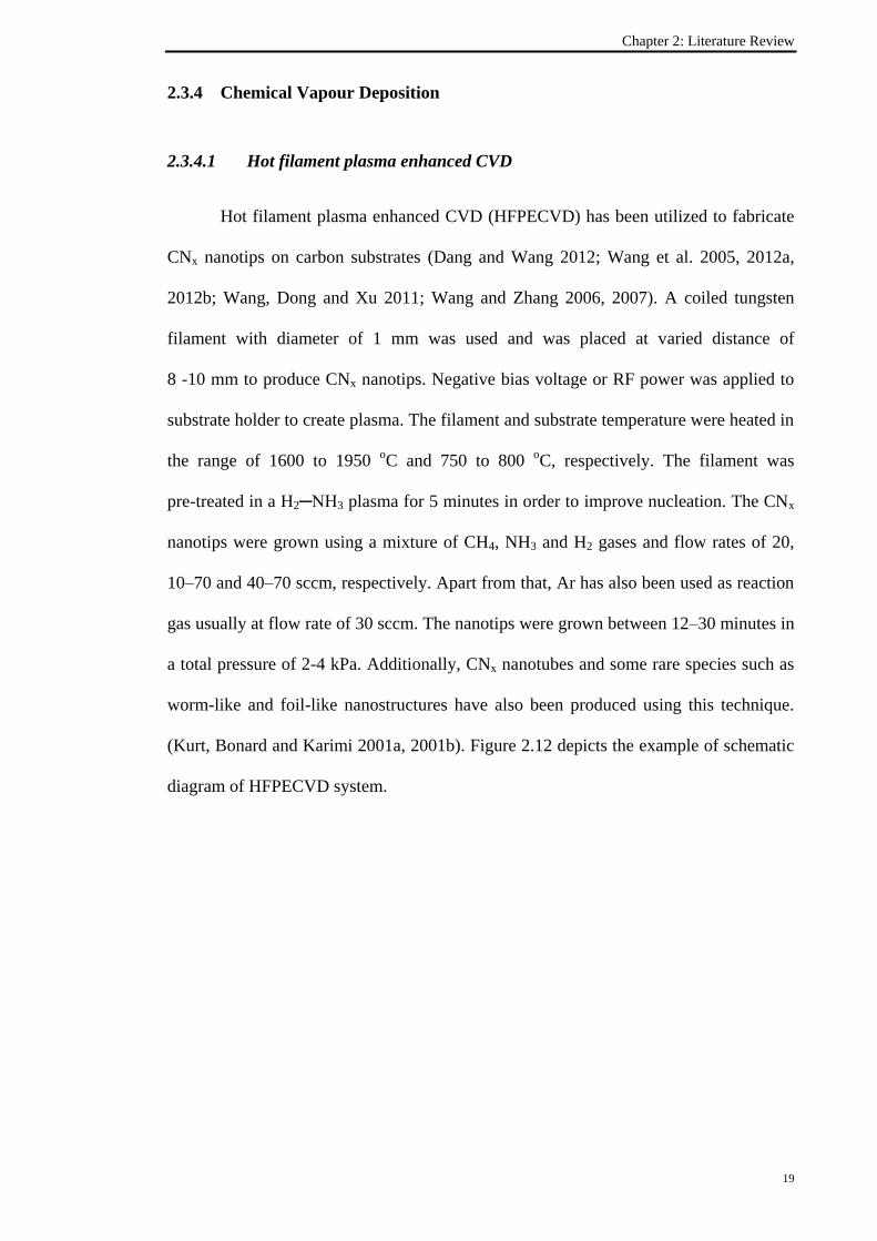
Hot filament plasma enhanced CVD (HFPECVD) has been utilized to fabricate
CNx nanotips on carbon substrates (Dang and Wang 2012; Wang et al. 2005, 2012a,
2012b; Wang, Dong and Xu 2011; Wang and Zhang 2006, 2007). A coiled tungsten
filament with diameter of 1 mm was used and was placed at varied distance of
8 -10 mm to produce CNx nanotips. Negative bias voltage or RF power was applied to
substrate holder to create plasma. The filament and substrate temperature were heated in
the range of 1600 to 1950 oC and 750 to 800
oC, respectively. The filament was
pre-treated in a H2─NH3 plasma for 5 minutes in order to improve nucleation. The CNx
nanotips were grown using a mixture of CH4, NH3 and H2 gases and flow rates of 20,
10–70 and 40–70 sccm, respectively. Apart from that, Ar has also been used as reaction
gas usually at flow rate of 30 sccm. The nanotips were grown between 12–30 minutes in
a total pressure of 2-4 kPa. Additionally, CNx nanotubes and some rare species such as
worm-like and foil-like nanostructures have also been produced using this technique.
(Kurt, Bonard and Karimi 2001a, 2001b). Figure 2.12 depicts the example of schematic
diagram of HFPECVD system.

Chapter 2: Literature Review
20
Figure 2.12: Example of schematic diagram of HFPECVD system.
2.3.4.2 Electron cyclotron resonance CVD
Electron cyclotron resonance CVD (ECRCVD) has been used to obtain CNx
nanotubes, CNx nanotips and vertically aligned amorphous CNx nanorods as reported by
Liu et al., Sung et al. and Lai et al. (Lai et al. 2003; Liu et al. 2000, 2002b; Sung et al.
1999). The CNx nanorods and nanotubes structures were deposited on anodic alumina
composite membrane with pore diameter 100-250 nm and 50-80 µm length which acts
as a template for the growth of the structure. All structures were prepared using a
mixture of C2H2 and N2 gases. The electron cyclotron resonance operated using a
microwave excitation at 2.45 GHz to generate plasma was fed perpendicularly through
the quartz dome into a magnetic field created by coils surrounding the chamber. It is
believed that ECRCVD provides the highest plasma density compared to other CVDs
(Wang et al. 2005) (Wang et al. 2012)
(Kurt, Bonard and Karimi, 2001a)
Chapter 2: Literature Review
21
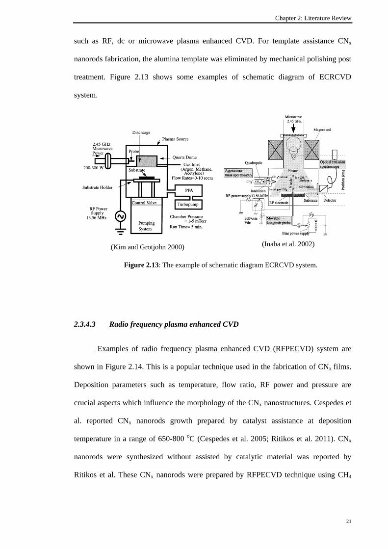
such as RF, dc or microwave plasma enhanced CVD. For template assistance CNx
nanorods fabrication, the alumina template was eliminated by mechanical polishing post
treatment. Figure 2.13 shows some examples of schematic diagram of ECRCVD
system.
Figure 2.13: The example of schematic diagram ECRCVD system.
2.3.4.3 Radio frequency plasma enhanced CVD
Examples of radio frequency plasma enhanced CVD (RFPECVD) system are
shown in Figure 2.14. This is a popular technique used in the fabrication of CNx films.
Deposition parameters such as temperature, flow ratio, RF power and pressure are
crucial aspects which influence the morphology of the CNx nanostructures. Cespedes et
al. reported CNx nanorods growth prepared by catalyst assistance at deposition
temperature in a range of 650-800 oC (Cespedes et al. 2005; Ritikos et al. 2011). CNx
nanorods were synthesized without assisted by catalytic material was reported by
Ritikos et al. These CNx nanorods were prepared by RFPECVD technique using CH4
(Kim and Grotjohn 2000) (Inaba et al. 2002)
Chapter 2: Literature Review
22
and N2 as precursor gases and deposited at different duration of 5 to 90 minutes on p-
type <111> Si substrate at low temperature ~100-200 oC and RF power of 60 W.
Figure 2.14: The schematic diagram of RFPECVD system.
2.3.4.4 Microwave plasma CVD
Examples of microwave plasma enhanced CVD (MWPECVD) is shown in
Figure 2.15. They are one of the common techniques which have been used in
producing ns-CNx including nanotubes and nanobells. Plasma was generated by the
microwave source working at frequency of 2.45 GHz. The CNx nanotubes could be
grown on Si substrate from a mixture of different gases such as CH4, C2H2, NH3 or N2
and are usually assisted by catalyst such as Fe and Ni. The deposition temperature,
pressure and gas flow rate ratio are critical parameters that influenced the formation of
the structures. Nanotubes and nanobells structures could be deposited on Si substrate at
temperature between 450–800 oC for 10 to 30 minutes at microwave power of
500–600 W and pressure of 2 kPa (Bai et al. 2001; Chan et al. 2003; Srivastava et al.
2006; Zhang et al. 2002; Zhong et al. 2001).
(Ritikos et al. 2009b) (Meyyappan et al. 2003)

Chapter 2: Literature Review
23
Figure 2.15: Example of schematic diagram of MWPECVD system.
2.3.4.5 Floating catalyst CVD
There are several works reported on the fabrication of CNx nanotubes and
nanofibers by using this technique. Usually single or multilayered catalyst such as Fe,
Ni, Al2O3 and MgO are used with carbon and nitrogen sources in a mixture of
acetonitrile and ethanol or CH4, NH3 and H2. The deposition of the films could take as
long as 8 to 60 minutes depending on the deposition conditions and temperature of the
substrate. The deposition requires pressure of the horizontal tube furnace to be in range
of 1 x 10⁻⁶
to 89 mbar. N2 or Ar gas is flowed into the tube before it was heated to the
desired temperature. When the entrance temperature increase to about 200 oC, the
precursor was introduced into the tube and evaporation begins. The temperature of the
furnace is increased up to 950 oC. The vapour was carried out by the gas flow to the
higher temperature region and thus the reaction occurrs. Then, the tube furnace is
allowed to cool down to room temperature (Ayala et al. 2007a, 2007b; He et al. 2005;
Koós et al. 2009; Liu et al. 2005, 2010; Maldonado, Morin and Stevenson 2006;
(Baehr et al. 1997) (Hung et al. 2011)
Chapter 2: Literature Review
24
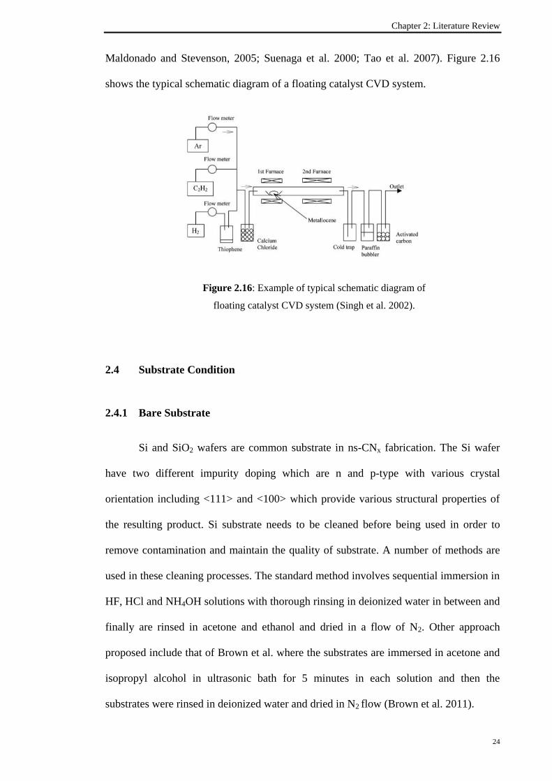
Maldonado and Stevenson, 2005; Suenaga et al. 2000; Tao et al. 2007). Figure 2.16
shows the typical schematic diagram of a floating catalyst CVD system.
Figure 2.16: Example of typical schematic diagram of
floating catalyst CVD system (Singh et al. 2002).
2.4 Substrate Condition
2.4.1 Bare Substrate
Si and SiO2 wafers are common substrate in ns-CNx fabrication. The Si wafer
have two different impurity doping which are n and p-type with various crystal
orientation including <111> and <100> which provide various structural properties of
the resulting product. Si substrate needs to be cleaned before being used in order to
remove contamination and maintain the quality of substrate. A number of methods are
used in these cleaning processes. The standard method involves sequential immersion in
HF, HCl and NH4OH solutions with thorough rinsing in deionized water in between and
finally are rinsed in acetone and ethanol and dried in a flow of N2. Other approach
proposed include that of Brown et al. where the substrates are immersed in acetone and
isopropyl alcohol in ultrasonic bath for 5 minutes in each solution and then the
substrates were rinsed in deionized water and dried in N2 flow (Brown et al. 2011).
Chapter 2: Literature Review
25
2.4.2 Catalyst
The use of catalytic materials to produce ns-CNx is a common practice. Usually,
transition metals such as Ni, Co, and Fe were used to achieve the desirable structures
(Lin et al. 2003; Sen et al. 1997). Catalyst preparation technique could be divided into
two types. The first is solution base preparation, such as dissolution, stirring,
precipitation, refluxing, separation, annealing or calcination. These techniques are
commonly used in CVD sample preparation. The second is physical method including
thermal evaporation, lithography, sputtering, transfer printing and combustion (Lin et al.
2003; Tao et al. 2007). These physical techniques are more widely used since they are
quicker, easier and enables small patterns compared to solution base techniques. There
are three factors affecting the formation of catalytic growth of ns-CNx. First, the
selection of catalyst where different materials formed different structures through the
precursor gases due to different catalytic reaction. Secondly, the effects of adsorption or
absorption on the catalyst surface due to the surface energy and its electronic state.
Finally, the structure of the catalyst including its size and crystallographic structure
(Lin et al. 2003). He et al. produced aligned nitrogen doped carbon nanotube by CVD
technique on Si substrate using Fe as catalyst and acetonitrile as precursor gas while Sen
et al. obtained CNx nanotubes by pyrolysis of pyridine on ~50 nm size of Co powder
(He et al. 2005; Sen et al. 1997). Ayala et al. used multilayered catalyst films which
promote the formation of vertically aligned nitrogen doped carbon nanotube prepared
from acetonitrile. These multilayered catalysts contain different metallic films made up
of Si, Al, MgO, Mo and Fe. The catalyst was then removed by mild sonication (Ayala et
al. 2007b). According to Brown et al., even though the purification method has been
enhanced recently, there are still few obstacles which should be resolved such as the
possibility of structural damage, the extra cost and process (Brown et al. 2011).
Chapter 2: Literature Review
26
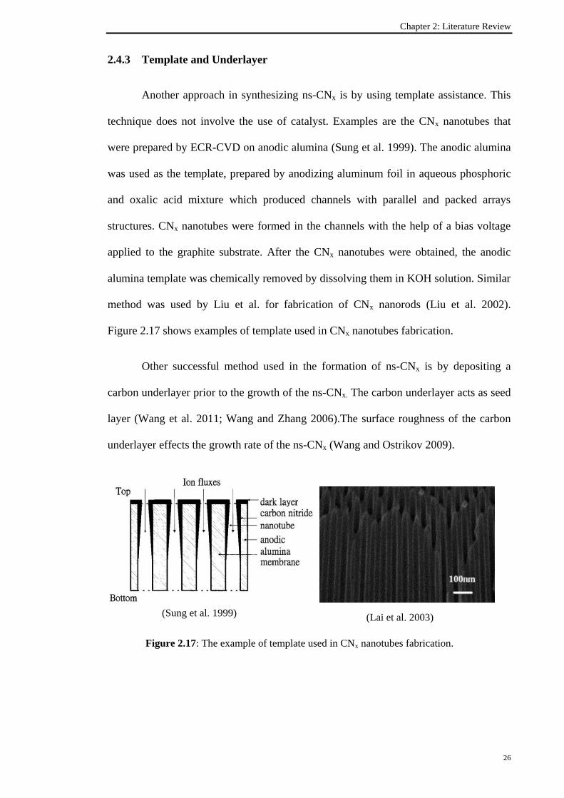
2.4.3 Template and Underlayer
Another approach in synthesizing ns-CNx is by using template assistance. This
technique does not involve the use of catalyst. Examples are the CNx nanotubes that
were prepared by ECR-CVD on anodic alumina (Sung et al. 1999). The anodic alumina
was used as the template, prepared by anodizing aluminum foil in aqueous phosphoric
and oxalic acid mixture which produced channels with parallel and packed arrays
structures. CNx nanotubes were formed in the channels with the help of a bias voltage
applied to the graphite substrate. After the CNx nanotubes were obtained, the anodic
alumina template was chemically removed by dissolving them in KOH solution. Similar
method was used by Liu et al. for fabrication of CNx nanorods (Liu et al. 2002).
Figure 2.17 shows examples of template used in CNx nanotubes fabrication.
Other successful method used in the formation of ns-CNx is by depositing a
carbon underlayer prior to the growth of the ns-CNx. The carbon underlayer acts as seed
layer (Wang et al. 2011; Wang and Zhang 2006).The surface roughness of the carbon
underlayer effects the growth rate of the ns-CNx (Wang and Ostrikov 2009).
(Sung et al. 1999) (Lai et al. 2003)
Figure 2.17: The example of template used in CNx nanotubes fabrication.

Chapter 2: Literature Review
27
2.5 Review of Analytical Methods
The following section reviews some of the analytical methods used in this work.
The review includes Fourier transform infrared (FTIR) and Raman scattering analysis.
Other methods including profilormeter measurement, atomic force microscopy (AFM),
field emission scanning electron microscopy (FESEM) and Auger electron spectroscopy
(AES) analysis are not discussed since they can be interpreted directly from images
and/or instrumental software.
2.5.1 Fourier Transform Infrared Spectroscopy
Fourier transform infrared (FTIR) spectroscopy is one of the common and
popular characterization tool widely used in the determination of bonding in a-C:H and
CNx. Any compound, either organic or inorganic has covalent bonds which would
absorb electromagnetic radiation in various specific frequencies in the infrared region.
The wavenumber of interest is in the region of 400-4000 cm-1
. The vibrational energy
transition for different bonding in a compound are assigned to specific value, thus could
be used as the „finger print‟ of the material. In general, there are a few types of
vibrational motion including stretching, bending, scissoring, wagging, rocking and
twisting. These are shown in Figure 2.18.

Chapter 2: Literature Review
28
Figure 2.18: Type of vibration mode in FTIR analysis (Marcelli et al. 2012).
From the FTIR spectrum obtained, the peak position and intensity of each bond
are assigned. However, the interpretation of the data should be done carefully since
there are some overlapping peaks which form broad peak thus clustering the shape and
the profile of the spectrum. Deconvolution method using Gaussian fitting has been used
extensively to solve this problem (Fanchini et al. 2005; Rodil 2005). Figures 2.19 and
2.20 show examples of typical FTIR spectra of a-C:H and CNx films.

Chapter 2: Literature Review
29
Figure 2.19: Example of typical FTIR spectrum of a-C:H film.
Figure 2.20: Example of typical FTIR spectrum of CNx film.
Chapter 2: Literature Review
30
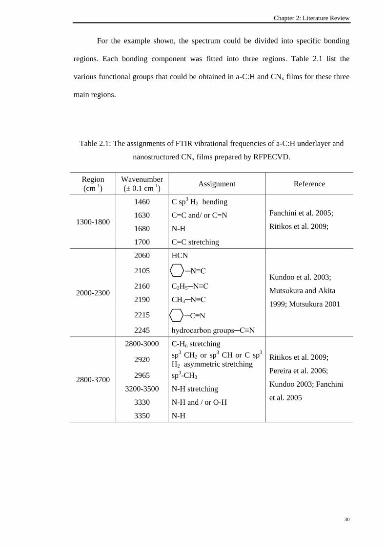
For the example shown, the spectrum could be divided into specific bonding
regions. Each bonding component was fitted into three regions. Table 2.1 list the
various functional groups that could be obtained in a-C:H and CNx films for these three
main regions.
Table 2.1: The assignments of FTIR vibrational frequencies of a-C:H underlayer and
nanostructured CNx films prepared by RFPECVD.
Region
(cm-1
)
Wavenumber
(± 0.1 cm-1
) Assignment Reference
1300-1800
1460 C sp3 H2 bending
Fanchini et al. 2005;
Ritikos et al. 2009;
1630 C=C and/ or C=N
1680 N-H
1700 C=C stretching
2000-2300
2060 HCN
Kundoo et al. 2003;
Mutsukura and Akita
1999; Mutsukura 2001
2105
2160 C2H5─N≡C
2190 CH3─N≡C
2215
2245 hydrocarbon groups─C≡N
2800-3700
2800-3000 C-Hn stretching
Ritikos et al. 2009;
Pereira et al. 2006;
Kundoo 2003; Fanchini
et al. 2005
2920 sp
3 CH2 or sp
3 CH or C sp
3
H2 asymmetric stretching
2965 sp3-CH3
3200-3500 N-H stretching
3330 N-H and / or O-H
3350 N-H
─C≡N
─N≡C
Chapter 2: Literature Review
31
2.5.2 Raman Spectroscopy
Raman spectra are associated with the structure of material. The various type of
carbon structure such as diamond, graphite, amorphous and others structures would give
different Raman spectra. Firstly, it is important to identify the general type of structure
according to its features. Example of typical Raman spectra for different types of
structure is presented in Figure 2.21 (Chu and Li 2006).
Typical Raman spectrum for carbon films shows two prominent peaks due to sp2
sites known as the D and G peak at Raman shift of 1360 and 1560 cm-1
, respectively.
However, there may also be one background peak at Raman shift of 1500 cm-1
typically
found for amorphous hydrogenated carbon (Huang et al. 2003). The D peak is attributed
to breathing modes of sixfold aromatic rings and only become active in the presence of
disorder. The G peak is due to bond stretching of all pairs of sp2 atoms both in rings and
chains (Escobar-Alarcón et al. 2005; Ferrari, Rodil and Robertson 2003; Ferrari 2007;
Zhao et al. 2011). There are four information which could be deduced from the Raman
analysis. This includes (a) sp2 phase clustering, (b) presence of sp
2 chains or rings, (c)
bond disorder and (d) relative content of sp2 and sp
3.
The Raman interpretation typically includes the deconvolution using Gaussian
fitting method (Marchon et al. 1997; Park et al. 2005). From this fittings, five
parameters can be extracted including its peak position and full width half maximum
(FWHM) of the D and G peaks and also the peak integrated intensities to calculate the
ID/IG ratio.
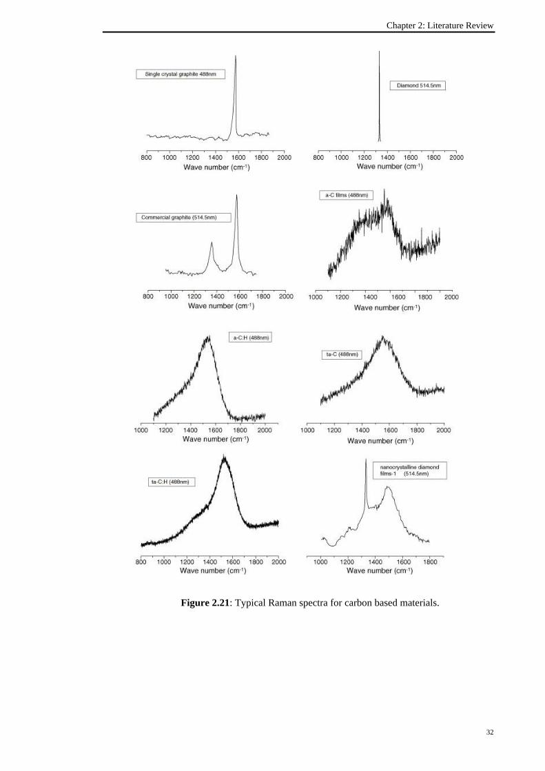
Chapter 2: Literature Review
32
Figure 2.21: Typical Raman spectra for carbon based materials.
Chapter 2: Literature Review
33
The red-shift (to higher wavenumber) in G peak position towards 1600 cm-1
being higher than that of graphite (1550 cm-1
) though not exceeding the limit of
graphitic carbon may imply that these films have high degree of graphitization. This
may also imply that the film exhibit characteristic of olefinic (chain sp2 group) with
shorter bond length (Gilkes et al. 1998). The blue shift (to lower wavenumber) in D
peak position can be attributed to the strained or curved graphite plane which occurs
when there is a change in the vibration frequency due to the change of spacing between
the atoms (Ferrari and Robertson 2000; Yu, Lee and Lee 2002).
A broadening in the width of the D peak (FWHMD) is correlated to the increase
in disorder due to the re-distribution of clusters with different orders and dimensions.
This is due to the presence of different order in the clusters. The FWHMG is also
sensitive to structural disorder though this is attributed to bond angle and bond length
distortion. If there is no defect within the cluster, the size of FWHMG would be small.
Conversely, an increase in bandwidth of both D and G, indicates lower degree of
clustering and less ordered structure (Zhao et al. 2011).
The ID/IG ratio depend on the size of the sp2 phase (Casiraghi et al. 2005).
According to Zhao et al, the low ID/ IG ratio (<1) in disordered graphite is due to the
decrement of defect or ordering of carbon atoms. This is attributed to small crystal size
or the destruction of symmetry in the crystalline structure. However in amorphous
carbon, the increase in ID/IG towards unity (ID/ IG ≈ 1) indicates an increase disorder or
decreasing crystallite size (Zhao et al. 2011). Further increase in ID/IG indicates an
increase in the number and/or size of graphitic cluster in the films (Ferrari and
Robertson 2000).

Chapter 3: Experimental and Analytical Techniques
34
CHAPTER 3 : EXPERIMENTAL AND ANALYTICAL TECHNIQUES
3.1 Introduction
In this work, carbon nitride (CNx) nanostructured films were prepared using
radio frequency plasma enhanced chemical vapour deposition (RFPECVD) technique.
This chapter presents the deposition procedures, experimental and analytical techniques
used in the characterization of the films. The first section focused on the RFPECVD
system, substrate preparation, film deposition and post deposition procedures. The
substrate preparation procedures consist of the substrate cleaning and pre-deposition
treatments. The next section discussed the characterization methods used, which include
atomic force microscopy (AFM), surface profilometer, scanning electron microscopy
(SEM), Fourier transform infrared (FTIR) spectroscopy, Raman spectroscopy and
Auger electron spectroscopy (AES).
3.2 Radio Frequency Plasma Enhanced Chemical Vapour Deposition System
The radio frequency plasma enhanced chemical vapour deposition which is
made up of a reaction chamber connected to three part subsystems consisting of a
vacuum system, gas distribution system and electrical system (Ritikos et al. 2009).
Figure 3.1 shows the schematic diagram of the RFPECVD system.
In this work, pure methane 99.995% (CH4), nitrogen 99.995% (N2) and
hydrogen 99.995% (H2) were used. The gases were flowed into the reaction chamber
through the sequence of line tubing and mass flow controllers (MFC) which are used to
control their flow rates. These MFCs operate at 0-200 standard cubic centimeter per
minute (sccm) for N2 and H2 while 0-50 sccm for CH4.
Chapter 3: Experimental and Analytical Techniques
35
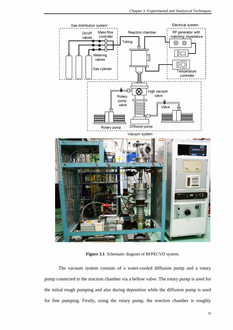
Figure 3.1: Schematic diagram of RFPECVD system.
The vacuum system consists of a water-cooled diffusion pump and a rotary
pump connected to the reaction chamber via a bellow valve. The rotary pump is used for
the initial rough pumping and also during deposition while the diffusion pump is used
for fine pumping. Firstly, using the rotary pump, the reaction chamber is roughly

Chapter 3: Experimental and Analytical Techniques
36
pumped to a base pressure of approximately at 3 x 10⁻³
mbar. During this time, the
diffusion pump is warmed up for about 30 minutes once the desired pressure is
achieved. The bellow valve direction of the pump is switched on and the pumping is
continued till the chamber pressure reached approximately to 5 x 10⁻⁵
mbar. The rotary
pump should be switched off immediately before the diffusion pump is operated to
avoid backflow due to difference in pressure.
The electrical system consists of a RF generator with a matching impedance
network, and also a temperature controller fitted with a heater power supply. The RF
generator is connected to the reaction chamber via the matching impedance which
balanced the different between impedance of the unit and the system. The substrate was
heated using (400 W) Watlow firerod cartridge heater driven by the ac power supply,
where the substrate temperature was measured using K-type thermocouple. The
temperature was monitored and controlled using a thermocouple and temperature
controller.
The main part in this RFPECVD system is the reaction chamber. Figure 3.2
shows the schematic diagram of this reaction chamber. This chamber is made from
stainless steel. The RF generator and gas distribution system are connected to the upper
part while the pumping system is attached to the bottom part of this chamber. The
electrode is arrayed in a parallel plate configuration. The upper electrode is a shower
head with holes size of about 1 mm and arrayed 1 cm apart. This electrode is connected
to the RF generator and is insulated from the chamber using a teflon block. The bottom
electrode which acts as the substrate holder, was electrically grounded and connected to
the heating component. The legs of the substrate holder are insulated by teflon cylinder
to avoid touching the body of the reaction chamber. Throughout this work, the distance
between the top and bottom electrode is fixed at 1 cm.

Chapter 3: Experimental and Analytical Techniques
37
1. Gas shower head 7. Thermocouple
2. Upper electrical feedthrough 8. Heater
3. Teflon 9. Substrate holder
4. Shower head 10. View port
5. Electrode distance 11. Lower electrical feedthrough
6. Substrate 12. Pressure gauge
Figure 3.2: Schematic diagram of RFPECVD system reaction chamber.

Chapter 3: Experimental and Analytical Techniques
38
3.3 Sample Preparation
3.3.1 Substrate Cleaning Procedures
The substrates were cleaved into rectangular pieces with dimension of 2.0 cm x
2.5 cm. The substrate cleaning is an important part in preparing the substrates for the
film deposition. Small amount of contamination on the substrate may change the
properties of the sample and also decrease the adhesion of the film onto the substrate. In
this work, all samples were deposited onto silicon (Si) substrate.
Firstly, the Si substrate was rinsed in deionized water and then soaked in a
solution of H2O:H2O2:HCl = 6:1:1 for 10 minutes. Then, these substrates were soaked
with deionized water in a beaker placed in an ultrasonic bath for 10 minutes. They were
soaked again in a solution of H2O:H2O2:NH4OH = 5:1:1 for 1 minute. After the
substrates were rinsed with deionized water, they were then immersed in a solution
H2O:HF = 10:1 for 1 minute. Finally, the substrates were rinsed with deionized water
and immersed in ethanol and then acetone before they were dried in a stream of nitrogen
gas and then placed in the deposition chamber. This whole process was done to remove
impurities and the oxide layer on the surface of these Si substrates.
3.3.2 Pre-deposition Process
The deposition chamber was thoroughly cleaned to remove all the deposits left
from the previous deposition process. Sand paper was used to remove the deposits on
the steel surface inside the chamber. The surface was then thoroughly cleaned with
acetone. The set up was assembled and the thermocouple and electrical connection were
attached to the substrate holder. Four clean substrates were positioned on the substrate
holder with a mask shown in Figure 3.3. The chamber was sealed and all the valves
were closed before the system is ready to be pumped down.
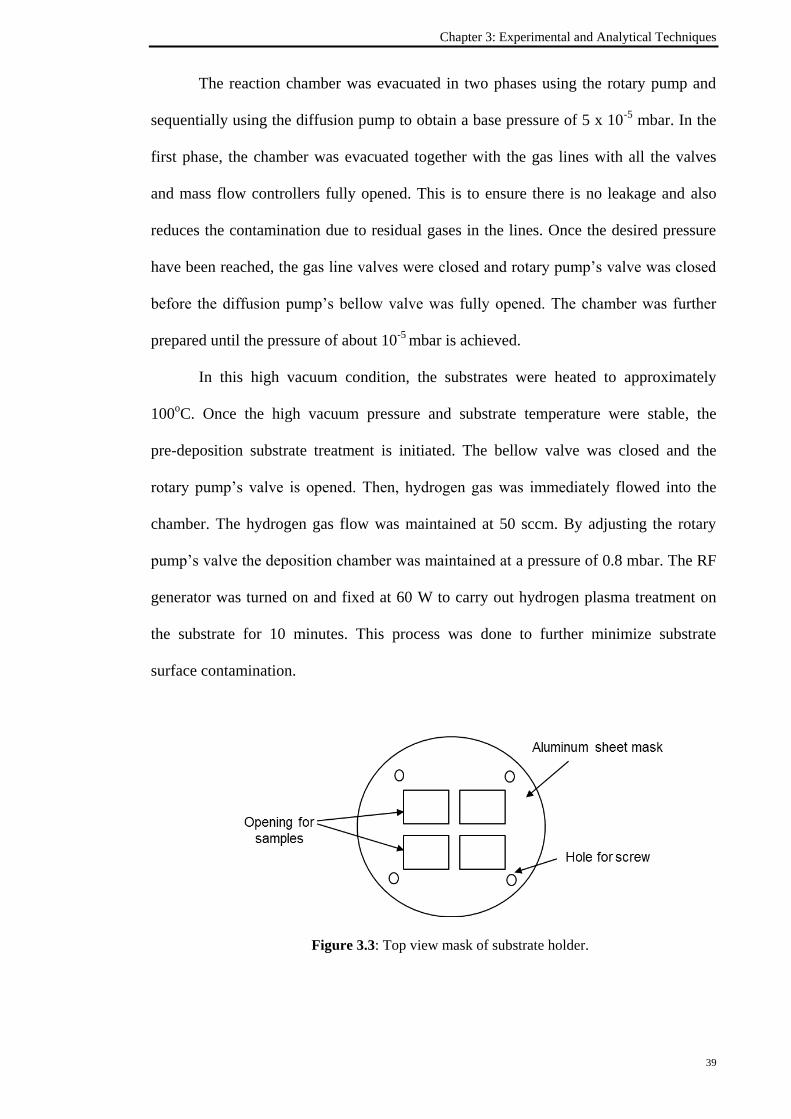
Chapter 3: Experimental and Analytical Techniques
39
The reaction chamber was evacuated in two phases using the rotary pump and
sequentially using the diffusion pump to obtain a base pressure of 5 x 10⁻⁵
mbar. In the
first phase, the chamber was evacuated together with the gas lines with all the valves
and mass flow controllers fully opened. This is to ensure there is no leakage and also
reduces the contamination due to residual gases in the lines. Once the desired pressure
have been reached, the gas line valves were closed and rotary pump‟s valve was closed
before the diffusion pump‟s bellow valve was fully opened. The chamber was further
prepared until the pressure of about 10-5
mbar is achieved.
In this high vacuum condition, the substrates were heated to approximately
100oC. Once the high vacuum pressure and substrate temperature were stable, the
pre-deposition substrate treatment is initiated. The bellow valve was closed and the
rotary pump‟s valve is opened. Then, hydrogen gas was immediately flowed into the
chamber. The hydrogen gas flow was maintained at 50 sccm. By adjusting the rotary
pump‟s valve the deposition chamber was maintained at a pressure of 0.8 mbar. The RF
generator was turned on and fixed at 60 W to carry out hydrogen plasma treatment on
the substrate for 10 minutes. This process was done to further minimize substrate
surface contamination.
Figure 3.3: Top view mask of substrate holder.

Chapter 3: Experimental and Analytical Techniques
40
3.3.3 Deposition Process
The film grown in this work consist of underlayer amorphous hydrogenated
carbon, a-C:H films and carbon nitride films which were deposited onto these a-C:H
underlayer; were grown by RFPECVD. Both configurations are shown in Figure 3.4.
These a-C:H underlayers were deposited from pure methane (99.995%) plasma. Where
there are variation in the a-C:H underlayer deposition, some of the parameter are fixed
throughout this work. This include the flow rate, deposition pressure and substrate
temperature of 20 sccm, 0.31 mbar and 100 oC, respectively. The CNx films were grown
on these a-C:H underlayer from the RF discharge of gas mixture of pure methane (CH4)
and nitrogen (N2) gas. The deposition parameters are fixed throughout this work. The
flow rate of the CH4 and N2 were fixed at 20 and 50 sccm respectively. The RF power
was fixed at 60 W while the deposition pressure was fixed at 0.58 mbar. Single a-C:H
underlayers were also fabricated to study the underlayers themselves.
c-Si a-C:H
c-Si a-C:H
c-Si
CNx
CH4 plasma [CH4 + N2]
plasma
Figure 3.4: Single a-C:H underlayer deposited on Si substrate and CNx film
deposited on a-C:H underlayer prepared by RFPECVD.

Chapter 3: Experimental and Analytical Techniques
41
Three sets of a-C:H underlayer and the subsequent CNx thin films were
prepared. In the first set, a-C:H underlayers were deposited at different deposition
duration of 5, 10, 15 and 30 minutes at RF power of 60 W. CNx films was deposited on
these a-C:H underlayers. In set 2, a-C:H underlayers were prepared at different RF
power of 30, 40, 50, 60, 80 and 100 W and deposited for 10 minutes. The last set
consists of a-C:H underlayers deposited at fixed RF power of 100 W and deposition
time of 10 minutes; and these are subsequently treated in hydrogen plasma for different
duration of 3, 5 and 10 minutes. The hydrogen plasma was produced from hydrogen at
flow rate 50 sccm. Subsequently CNx films were deposited onto these films and the
effects of varying each deposition condition were studied in terms of the a-C:H
underlayer and the CNx formation. The chart of the set of samples prepared in this work
is shown in Figure 3.5. Table 3.1 summarizes the parameters for a-C:H layer and CNx
film.

Chapter 3: Experimental and Analytical Techniques
42
c-Si
a-C:H c-Si
a-C:H c-Si
CNx
Set 1
a-C:H underlayers
deposited on c-Si for
deposition duration of 5,
10, 15 and 30 minutes at
fixed RF power of 60 W
Set 2
a-C:H underlayers
deposited on c-Si
substrate at RF power of
30, 40, 50, 60, 80 and
100 W for 10 minutes
Set 3
a-C:H underlayers
deposited on c-Si
substrate at RF power of
100 W for 10 minutes
with different H2
treatment time of 3, 5 and
10 minutes
Set 1
Subsequent CNx film on
a-C:H underlayers
deposited at different
deposition time of 5, 10,
15 and 30 minutes.
Set 2
Subsequent CNx film on
a-C:H underlayers
deposited at RF power of
30, 40, 50, 60, 80 and
100 W for 10 minutes
Set 3
Subsequent CNx film on
a-C:H underlayers
deposited at RF power of
100 W for 10 minutes
with different H2
treatment time of 3, 5 and
10 minutes
Figure 3.5: Chart of sample preparation.
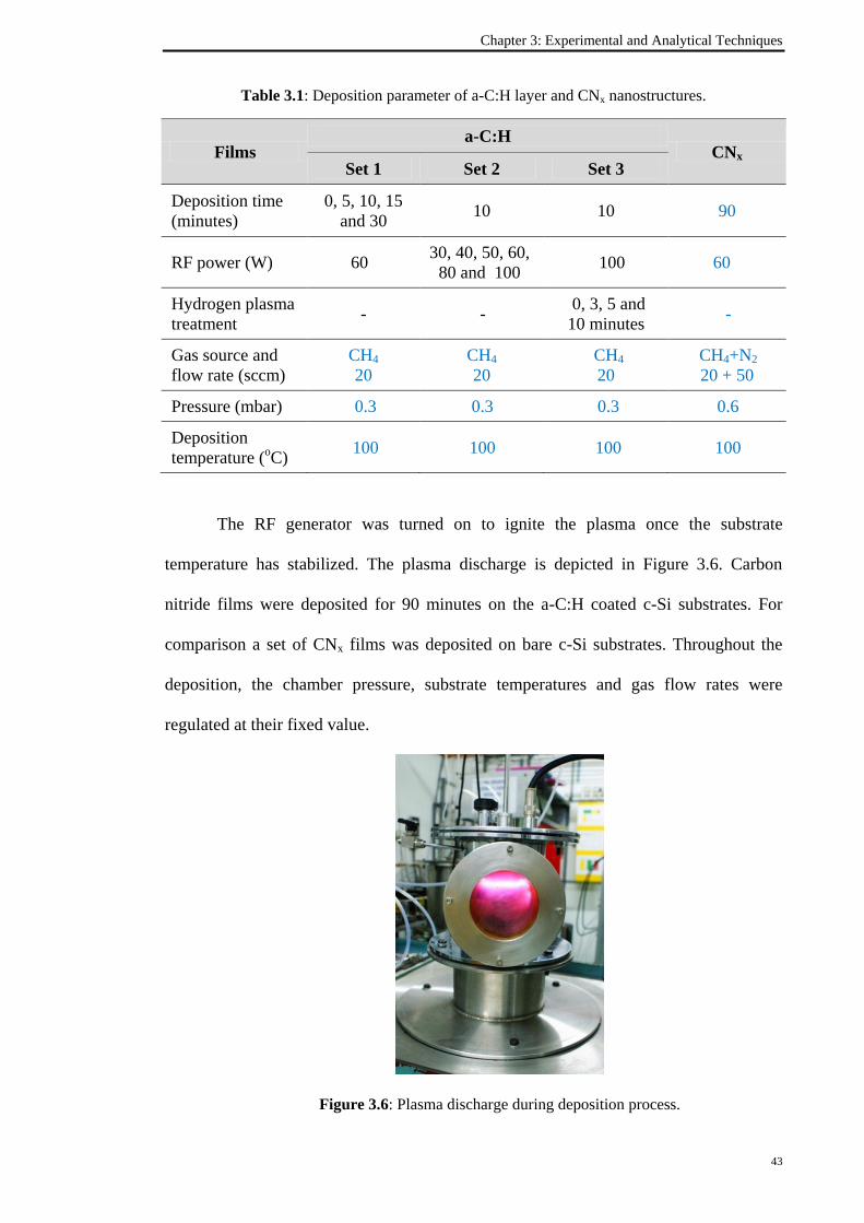
Chapter 3: Experimental and Analytical Techniques
43
Table 3.1: Deposition parameter of a-C:H layer and CNx nanostructures.
Films a-C:H
CNx Set 1 Set 2 Set 3
Deposition time
(minutes)
0, 5, 10, 15
and 30 10 10 90
RF power (W) 60 30, 40, 50, 60,
80 and 100 100 60
Hydrogen plasma
treatment - -
0, 3, 5 and
10 minutes -
Gas source and
flow rate (sccm)
CH4
20
CH4
20
CH4
20
CH4+N2
20 + 50
Pressure (mbar) 0.3 0.3 0.3 0.6
Deposition
temperature (oC)
100 100 100 100
The RF generator was turned on to ignite the plasma once the substrate
temperature has stabilized. The plasma discharge is depicted in Figure 3.6. Carbon
nitride films were deposited for 90 minutes on the a-C:H coated c-Si substrates. For
comparison a set of CNx films was deposited on bare c-Si substrates. Throughout the
deposition, the chamber pressure, substrate temperatures and gas flow rates were
regulated at their fixed value.
Figure 3.6: Plasma discharge during deposition process.
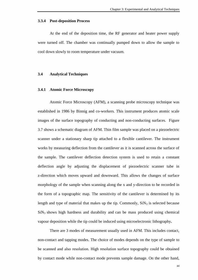
Chapter 3: Experimental and Analytical Techniques
44
3.3.4 Post-deposition Process
At the end of the deposition time, the RF generator and heater power supply
were turned off. The chamber was continually pumped down to allow the sample to
cool down slowly to room temperature under vacuum.
3.4 Analytical Techniques
3.4.1 Atomic Force Microscopy
Atomic Force Microscopy (AFM), a scanning probe microscopy technique was
established in 1986 by Binnig and co-workers. This instrument produces atomic scale
images of the surface topography of conducting and non-conducting surfaces. Figure
3.7 shows a schematic diagram of AFM. Thin film sample was placed on a piezoelectric
scanner under a stationary sharp tip attached to a flexible cantilever. The instrument
works by measuring deflection from the cantilever as it is scanned across the surface of
the sample. The cantilever deflection detection system is used to retain a constant
deflection angle by adjusting the displacement of piezoelectric scanner tube in
z-direction which moves upward and downward. This allows the changes of surface
morphology of the sample when scanning along the x and y-direction to be recorded in
the form of a topographic map. The sensitivity of the cantilever is determined by its
length and type of material that makes up the tip. Commonly, SiN3 is selected because
SiN3 shows high hardness and durability and can be mass produced using chemical
vapour deposition while the tip could be induced using microelectronic lithography.
There are 3 modes of measurement usually used in AFM. This includes contact,
non-contact and tapping modes. The choice of modes depends on the type of sample to
be scanned and also resolution. High resolution surface topography could be obtained
by contact mode while non-contact mode prevents sample damage. On the other hand,

Chapter 3: Experimental and Analytical Techniques
45
tapping mode is preferred because its combines the advantages of both contact and non-
contact modes. This minimizes damage of the film surface while producing high
resolution image. A VEECO Dimension 3000 atomic force microscope as shown in
Figure 3.8, was used to determine the surface roughness and morphological properties
of the a-C:H underlayer.
Figure 3.7: Schematic diagram of AFM
Figure 3.8: VEECO Dimension 3000 atomic force microscope.

Chapter 3: Experimental and Analytical Techniques
46
An a-C:H underlayer was scanned within an area of 5 x 5 m2. Figure 3.9 (a)
and (b) show a typical surface morphological image and the corresponding roughness
analysis respectively.
Figure 3.9: Surface morphological (a) and roughness analysis (b) of a-C:H underlayer
deposited by RFPECVD at 10 minutes.
(a)
(b)
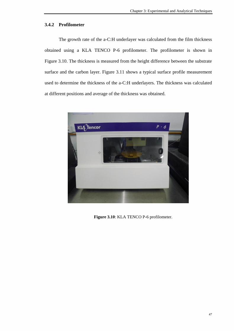
Chapter 3: Experimental and Analytical Techniques
47
3.4.2 Profilometer
The growth rate of the a-C:H underlayer was calculated from the film thickness
obtained using a KLA TENCO P-6 profilometer. The profilometer is shown in
Figure 3.10. The thickness is measured from the height difference between the substrate
surface and the carbon layer. Figure 3.11 shows a typical surface profile measurement
used to determine the thickness of the a-C:H underlayers. The thickness was calculated
at different positions and average of the thickness was obtained.
Figure 3.10: KLA TENCO P-6 profilometer.

Chapter 3: Experimental and Analytical Techniques
48
Figure 3.11: Data observed from profilometer for film deposited at 100 W
RF power with 3 minutes hydrogen treatment process.
3.4.3 Scanning Electron Microscopy
High resolution surface and cross section of images of the CNx films were
obtained from a FEI Quanta 200 field emission scanning electron microscope (FESEM).
The FESEM is shown in Figure 3.12. The FESEM operates using a beam of electron
which is scanned across a sample. During the scanning process, the specimen is
bombarded with electrons. The electrons may be elastically reflected or absorbed by the
sample. Secondary electrons and x-rays can be produced from the specimen surface if
the incident beam is energetic enough. This causes a slight energy loss and path change
in the incident electrons and ionization of electron in the specimen atom. Several
secondary electrons can be produced by each of the incident electrons and all these
effects can be used to produce an image.
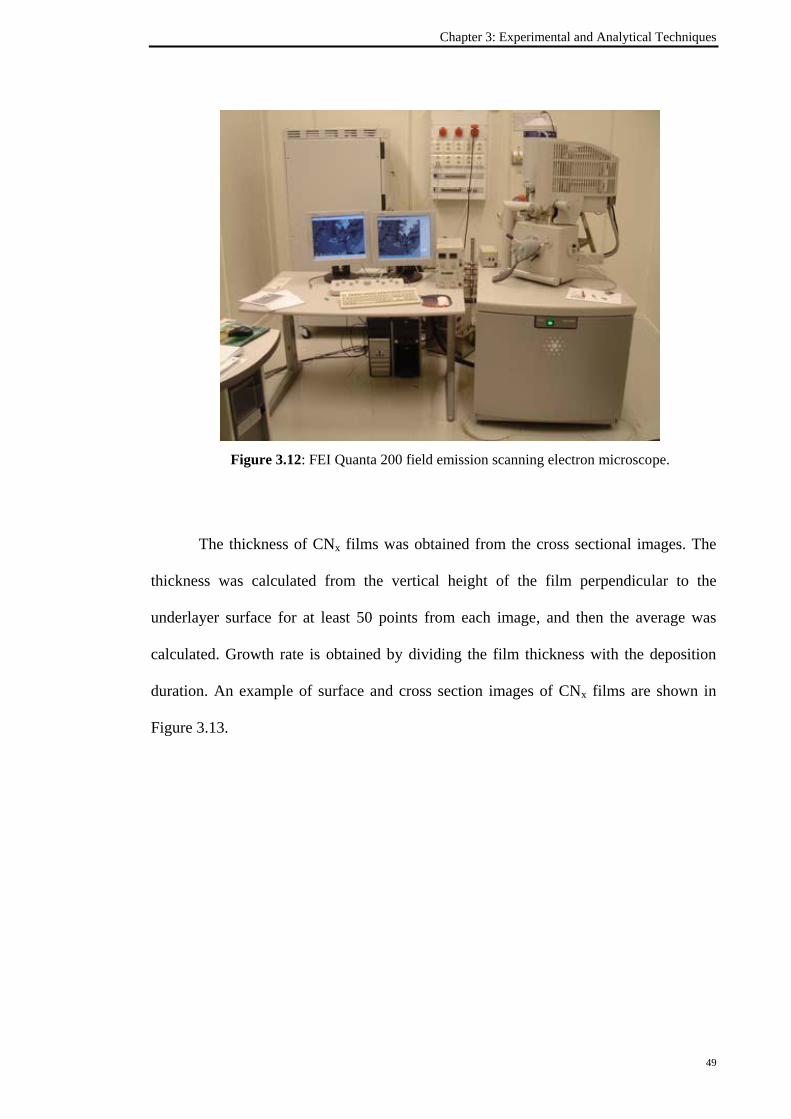
Chapter 3: Experimental and Analytical Techniques
49
Figure 3.12: FEI Quanta 200 field emission scanning electron microscope.
The thickness of CNx films was obtained from the cross sectional images. The
thickness was calculated from the vertical height of the film perpendicular to the
underlayer surface for at least 50 points from each image, and then the average was
calculated. Growth rate is obtained by dividing the film thickness with the deposition
duration. An example of surface and cross section images of CNx films are shown in
Figure 3.13.

Chapter 3: Experimental and Analytical Techniques
50
(a) (b)
Figure 3.13: Surface (a) and cross section (b) images of CNx film deposited on a-C:H
underlayer prepared at RF power of 50 W.
3.4.4 Fourier Transform Infrared Spectroscopy Measurement
Fourier Transform Infrared (FTIR) spectroscopy, is used to determine the
chemical bonding structure and molecule content in the a-C:H underlayer and CNx thin
film. The FTIR technique is used to identify the absorption of various bonding of the a-
C:H and CNx films. This was done by measuring the infrared radiations by the sample
under transmission mode. Molecular vibrations give rise to IR bands only if they cause
a change in the dipole moment of the molecule which includes stretching, wagging,
rocking and bending. The normal way to interpret an IR spectrum is to identify
functional group regions, then to note any unusually strong bands or particularly
prominent patterns in the fingerprint region. These functional groups could be identified
from the spectra with reference to those obtained from literature. Figure 3.14 shows the
schematic diagram of Fourier Transform Infrared Spectrometer. The interferogram is a
complex signal produced from an optical pathway pattern. This signal is generated by
combination of two beams oriented toward the sample by a beam splitter. The sample
absorbs the beam that passes through at specific wavelength and the computer compares
the signal produced with a reference laser beam. The resulting interferogram shows all

Chapter 3: Experimental and Analytical Techniques
51
the information in an imaginary one time-domain signal. A mathematical process called
Fourier transform is applied by the computer to produce the resulting infrared spectrum.
Figure 3.14: Schematic diagram of Fourier Transform Infrared Spectrometer.
FTIR measurements were done using a Perkin Elmer System 2000 FTIR
spectrometer in transmission mode as shown in Figure 3.15. The sample deposited on Si
substrate was scanned in the range of 400-4000 cm-1
. A blank Si substrate was used as
background. The spectrum is converted to absorption spectrum by normalizing it to film
thickness.

Chapter 3: Experimental and Analytical Techniques
52
Figure 3.15: The Perkin Elmer System 2000 FTIR spectrometer.
Figure 3.16 shows a typical FTIR spectrum of a-C:H underlayer while
Figure 3.17 shows a typical FTIR spectrum for CNx nanostructures. These spectra are
divided into 2 and 3 regions at wavenumber respectively of 1300-1800, 2000-2300 and
2800-3700 cm-1
. Each region is assigned to bonds accordingly as shown in Table 2.1.
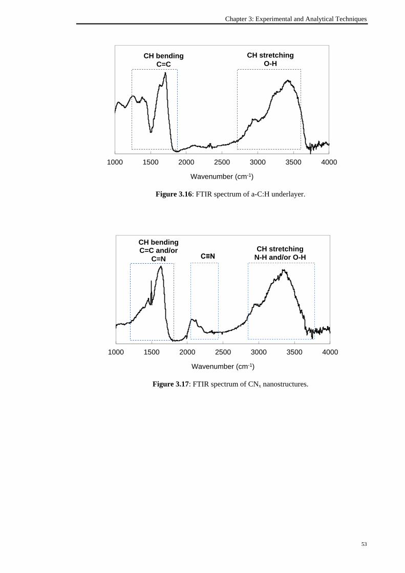
Chapter 3: Experimental and Analytical Techniques
53
Figure 3.16: FTIR spectrum of a-C:H underlayer.
Figure 3.17: FTIR spectrum of CNx nanostructures.
1000 1500 2000 2500 3000 3500 4000
Wavenumber (cm-1)
1000 1500 2000 2500 3000 3500 4000
Wavenumber (cm-1)
CH bending C=C and/or
C=N C≡N CH stretching
N-H and/or O-H
CH bending C=C
CH stretching O-H

Chapter 3: Experimental and Analytical Techniques
54
The spectrum was deconvoluted according to those proposed by other
researchers (Mutsukura and Akita 1999; Fanchini et al. 2005; Li et al. 2006) to obtain
the integrated intensity of the absorption spectra This integrated intensity can be
determined from the following relation.
The absorption coefficient is given by equation 3.1.
= ln (3.1)
where d is the film thickness and T is the transmittance.
The integrated intensity of the absorption band representing a particular bonding
configuration is obtained using equation 3.2.
I= d (3.2)
The Gaussian or Doppler line shape was used to deconvolute the component peak from
the absorption spectrum. This can be expressed using
( ) = max exp (3.3)
with max = (3.4)
and Sband = (3.5)
Sband, , ( ) and are the area under the spectrum, the full width half maximum
(FWHM) of the absorption peak, the maximum absorption coefficient and the position
of absorption peak respectively. Equation 3.2 can be rewritten in the form of
y = A exp (-Bx) (3.6)
where A, B and x can be expressed in the following form
y = ( ) (3.7)
x = ( )2
(3.8)
A = , or A = (3.9)
d
1
T%
100
0
)(
2
2
0
)(
))(2(ln4
)(
)2(ln2
21
21
bandS
d)(
0
0
21
21
bandSB
)(
)2(ln2
21
21
bandS
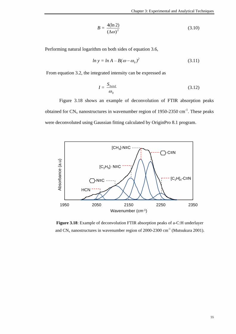
Chapter 3: Experimental and Analytical Techniques
55
B = (3.10)
Performing natural logarithm on both sides of equation 3.6,
ln y = ln A – B( )2 (3.11)
From equation 3.2, the integrated intensity can be expressed as
I = (3.12)
Figure 3.18 shows an example of deconvolution of FTIR absorption peaks
obtained for CNx nanostructures in wavenumber region of 1950-2350 cm-1
. These peaks
were deconvoluted using Gaussian fitting calculated by OriginPro 8.1 program.
Figure 3.18: Example of deconvolution FTIR absorption peaks of a-C:H underlayer
and CNx nanostructures in wavenumber region of 2000-2300 cm-1
(Mutsukura 2001).
2)(
)2(ln4
0
0bandS
HCN
-N≡C
[C2H5]- N≡C
[CH3]-N≡C
-C≡N
[C2H]n-C≡N
1950 2050 2150 2250 2350
Ab
so
rban
ce
(a.u
)
Wavenumber (cm-1)

Chapter 3: Experimental and Analytical Techniques
56
3.4.5 Raman Spectroscopy
Raman Spectroscopy is used to study the vibrational, rotational and other low
frequency transition properties of materials. The Raman effect occurs when frequency
of monochromatic light changes upon interaction with a sample due to an inelastic
scattering of the monochromatic laser source. The sample absorbs the photon from the
laser source and reemitted photon and the difference in frequency of incident and
emitted photon provides information about the vibrational and rotational transition in
molecules.
Figure 3.19 shows the Renishaw inVia Raman Microscope and in this work
measurements were carried out by using Helium-Cadmium laser with excitation
wavelength of 325 nm and grating slit of 2400 lines/mm for film deposited on c-Si
substrate. Raman shift was determined in wavenumber range of 1000-2500 cm-1
measured at an exposed time of 10 s at laser power of approximately 0.2 mW.
Figure 3.19: The Renishaw inVia Raman Microscope.
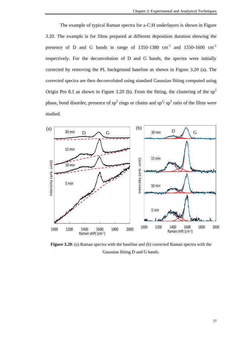
Chapter 3: Experimental and Analytical Techniques
57
The example of typical Raman spectra for a-C:H underlayers is shown in Figure
3.20. The example is for films prepared at different deposition duration showing the
presence of D and G bands in range of 1350-1380 cm-1
and 1550-1600 cm-1
respectively. For the deconvolution of D and G bands, the spectra were initially
corrected by removing the PL background baseline as shown in Figure 3.20 (a). The
corrected spectra are then deconvoluted using standard Gaussian fitting computed using
Origin Pro 8.1 as shown in Figure 3.20 (b). From the fitting, the clustering of the sp2
phase, bond disorder, presence of sp2 rings or chains and sp
2/ sp
3 ratio of the films were
studied.
Figure 3.20: (a) Raman spectra with the baseline and (b) corrected Raman spectra with the
Gaussian fitting D and G bands.
(a) (b) D G G D
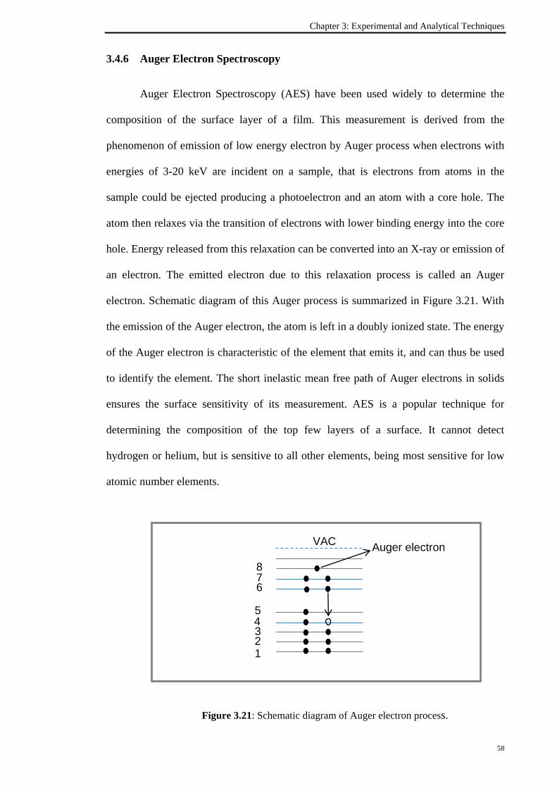
Chapter 3: Experimental and Analytical Techniques
58
3.4.6 Auger Electron Spectroscopy
Auger Electron Spectroscopy (AES) have been used widely to determine the
composition of the surface layer of a film. This measurement is derived from the
phenomenon of emission of low energy electron by Auger process when electrons with
energies of 3-20 keV are incident on a sample, that is electrons from atoms in the
sample could be ejected producing a photoelectron and an atom with a core hole. The
atom then relaxes via the transition of electrons with lower binding energy into the core
hole. Energy released from this relaxation can be converted into an X-ray or emission of
an electron. The emitted electron due to this relaxation process is called an Auger
electron. Schematic diagram of this Auger process is summarized in Figure 3.21. With
the emission of the Auger electron, the atom is left in a doubly ionized state. The energy
of the Auger electron is characteristic of the element that emits it, and can thus be used
to identify the element. The short inelastic mean free path of Auger electrons in solids
ensures the surface sensitivity of its measurement. AES is a popular technique for
determining the composition of the top few layers of a surface. It cannot detect
hydrogen or helium, but is sensitive to all other elements, being most sensitive for low
atomic number elements.
5
3 2
4
1
VAC
6
8 7
Auger electron
Figure 3.21: Schematic diagram of Auger electron process.
Chapter 3: Experimental and Analytical Techniques
59
In this work, Auger electron was measured by JAMP-9500F Field Emission
Auger Microprobe, as shown in Figure 3.22. Etching and measure cycles were carried
out to obtain reliable, consistent result, since the top surface of the film tends to have
contamination. The etching process is done by sputtering of high energy heavy ion
beam in which Ar+ ions was used to impinge the surface of the film. Figure 3.23
illustrates the typical AES spectra of CNx nanostructured films. In this example, the
films are prepared at different deposition duration for the a-C:H underlayer. From the
quantitative analysis, the nitrogen to carbon content ratio was calculated.

Chapter 3: Experimental and Analytical Techniques
60
Figure 3.22: JAMP-9500F Field Emission Auger Microprobe.
Figure 3.23: AES spectra variation of CNx prepared on different deposition
duration of a-C:H underlayer and bare c-Si substrate.
c-Si
5 min
15 min
30 min
10 min
0 100 200 300 400 500 600 700 800 900 1000
Inte
nsity (
a.u
)
Energy (eV)
Chapter 4: Results and Discussion
61
CHAPTER 4 : EFFECTS OF HYDROGENATED AMORPHOUS CARBON
UNDERLAYER ON THE FORMATION OF CARBON
NITRIDE NANOSTRUCTURES: RESULTS, ANALYSIS AND
DISCUSSION
4.1 Introduction
This chapter presents the experiment results, analysis and discussion related to
the study of hydrogenated amorphous carbon (a-C:H) thin films used as the underlayer
film in the subsequent fabrication of carbon nitride nanostructures (ns-CNx). These
films were deposited using radio frequency plasma enhanced chemical vapour
deposition (RFPECVD) from the precursors methane and nitrogen gases. For the a-C:H
underlayers, their growth rate, surface roughness , chemical bonding and structural
properties were studied. Subsequently, ns-CNx were grown directly onto these a-C:H
underlayer films. These ns-CNx/a-C:H films were studied in terms of their surface and
cross section images, growth rates, elemental composition and bonding properties.
This exploratory study focuses on three different aspects of the a-C:H underlayer
growth and treatment. The first aspect looks into the effects of growth duration on these
underlayer films, then the effects of the morphology of the underlayer on the formation
of the ns-CNx were studied. While the deposition time duration is varied, other critical
deposition parameters such as the RF power, gas ratios, deposition temperatures and
pressures, were kept constant. These critical parameters are known to significantly
influence the structure of the film and thus it is expected that by keeping them constant
throughout the deposition, the bulk structure of the films themselves should remain
constant. This may enable studies of the growth and surface morphology to be
scrutinized.
Chapter 4: Results and Discussion
62
The second part looks into one of these critical deposition parameters, namely
the effect of applied RF power on the deposition of the a-C:H underlayer and
corresponding ns-CNx. This was carried out while keeping the rest of the parameters
constant, including the deposition duration. The third part looks into a totally different
aspect. This involves the effect of hydrogen treatment onto a particular a-C:H
underlayer sample. The as-deposited sample chosen exhibited the smoothest surface.
The purpose of the treatment is to determine the potential of using surface treatment to
alter the a-C:H surface and subsequently to produce different ns-CNx structures.
In each part, the results and discussion were first focused on the characterization
of the a-C:H underlayer films, followed by the characterization of the subsequent
formation of ns-CNx. The discussion in these part includes the correlation of the
properties of the a-C:H underlayers and the structure of the ns-CNx. Figure 4.1
summarizes the methodology and variations in the parameters involved in the
modification of the a-C:H underlayer.

Chapter 4: Results and Discussion
63
a-C:H underlayer
Varied = deposition
duration
bare c-Si 10 min 5 min 15 min 30 min
a-C:H underlayer
Varied = RF power
30 W 50 W 40 W 80 W 100 W
a-C:H underlayer
Varied = H2 plasma
treatment duration
As deposited 3 min 5 min 10 min
ns-CNx
ns-CNx
ns-CNx
Preparation of a-C:H
underlayer film
Subsequent deposition
of ns-CNx film
Fixed parameters:
Duration = 10 min
CH4 = 20 sccm
Pressure = 0.3 mbar
Temperature = 100oC
Fixed parameters:
??????
Fixed parameters:
RF power = 60 W
CH4 = 20 sccm
Pressure = 0.3 mbar
Temperature = 100oC
Common Fixed parameters:
RF power = 60 W
CH4 + N2 = 20 + 50 sccm
Pressure = 0.6 mbar
Temperature = 100oC
Duration = 90 min
Figure 4.1: Summary of the methodology and variations in film preparation parameters.
Duration = 10 min
CH4 = 20 sccm
Pressure = 0.3 mbar
RF power = 100 W
Temperature = 100oC
Variable:
Variable:
Variable:
Chapter 4: Results and Discussion
64
4.2 Effects of Deposition Time Duration of a-C:H Underlayer and Resulting
CNx/ a-C:H Formation
The first study focuses on the effects of different deposition time duration on the
properties of a-C:H underlayers and thus its effects on the properties of the ns-CNx. Five
sets of samples are prepared where the deposition duration for a-C:H underlayers was
varied at 5, 10, 15, 30 minutes, together with a CNx prepared on bare c-Si. The growth
rate, morphology, chemical bonding properties and composition of the films were
studied.
4.2.1 Effects of Deposition Time Duration on a-C:H Underlayers
4.2.1.1 Growth rate of a-C:H underlayers
The thickness of these a-C:H underlayers were determined from surface profiler
measurement. Figure 4.2 presents the variation of thickness and deposition rate of a-C:H
underlayer deposited as a function of deposition time duration (tD). The thickness of the
a-C:H underlayers increase gradually at tD up to 10 minutes, and subsequently increased
linearly up to tD of 30 minutes. The growth rates of these a-C:H films were calculated
from the thickness. The growth rate decreased slightly when tD was increased from 5 to
10 minutes and then, with further increase in tD an almost constant increase in the
growth rate was observed.
The growth rate of the a-C:H underlayers by RFPECVD is dependent on the
number of nucleation sites present for the diffusion of carbon growth radicals from the
plasma. The creation of the nucleation sites is mainly contributed by hydrogen etching
effects and/or ion bombardment and abstraction process by CH3 radicals. These

Chapter 4: Results and Discussion
65
effectively break weak C-C bonds or H terminated bonds (Si-H on the c-Si substrates or
C-H bonds), creating dangling bonds which allowed C growth radicals to bond onto the
film. The slight decrease in growth rate for the film deposited at tD of 10 minutes
indicates that the rate of nucleation sites formation was larger than the rate of diffusion
of C growth radicals onto these nucleation sites. Longer deposition duration increased
the number of growth radicals reaching the growth sites thus increased the growth rate
of the film.
Figure 4.2: Thickness (■) and growth rate (♦) of a-C:H underlayer deposited by RFPECVD for
different deposition time duration. The line is only an eye-guide.
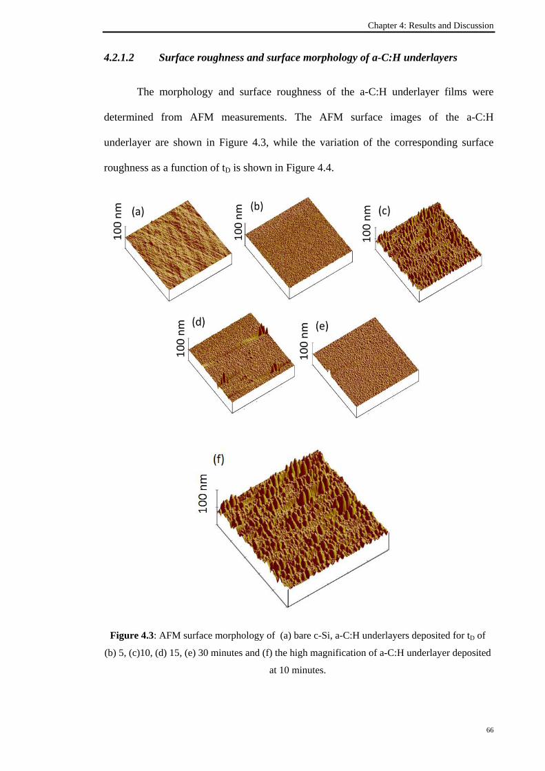
Chapter 4: Results and Discussion
66
4.2.1.2 Surface roughness and surface morphology of a-C:H underlayers
The morphology and surface roughness of the a-C:H underlayer films were
determined from AFM measurements. The AFM surface images of the a-C:H
underlayer are shown in Figure 4.3, while the variation of the corresponding surface
roughness as a function of tD is shown in Figure 4.4.
Figure 4.3: AFM surface morphology of (a) bare c-Si, a-C:H underlayers deposited for tD of
(b) 5, (c)10, (d) 15, (e) 30 minutes and (f) the high magnification of a-C:H underlayer deposited
at 10 minutes.
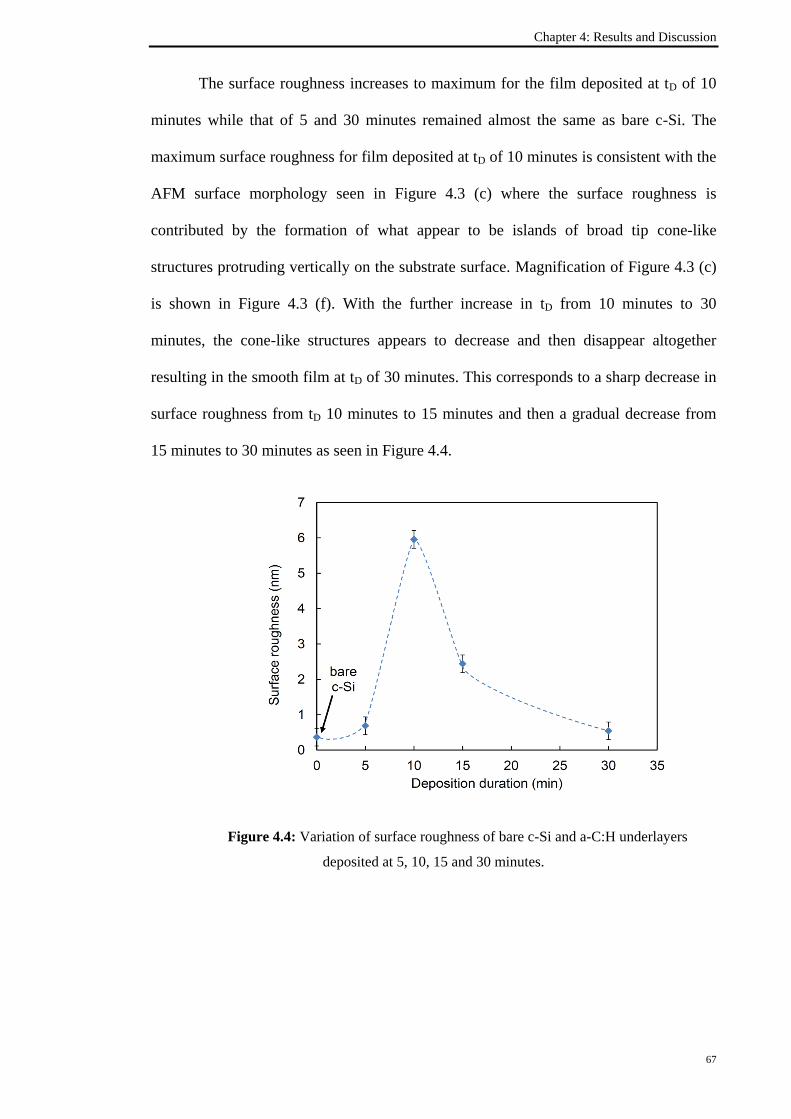
Chapter 4: Results and Discussion
67
The surface roughness increases to maximum for the film deposited at tD of 10
minutes while that of 5 and 30 minutes remained almost the same as bare c-Si. The
maximum surface roughness for film deposited at tD of 10 minutes is consistent with the
AFM surface morphology seen in Figure 4.3 (c) where the surface roughness is
contributed by the formation of what appear to be islands of broad tip cone-like
structures protruding vertically on the substrate surface. Magnification of Figure 4.3 (c)
is shown in Figure 4.3 (f). With the further increase in tD from 10 minutes to 30
minutes, the cone-like structures appears to decrease and then disappear altogether
resulting in the smooth film at tD of 30 minutes. This corresponds to a sharp decrease in
surface roughness from tD 10 minutes to 15 minutes and then a gradual decrease from
15 minutes to 30 minutes as seen in Figure 4.4.
Figure 4.4: Variation of surface roughness of bare c-Si and a-C:H underlayers
deposited at 5, 10, 15 and 30 minutes.

Chapter 4: Results and Discussion
68
4.2.1.3 Chemical bonding properties of a-C:H underlayers
FTIR spectra were obtained to study the chemical bonding of the a-C:H
underlayers. The FTIR spectra for the films prepared at different tD are shown in
Figure 4.5. The spectra can be separated into 2 main regions at wavenumber ranges of
1200-1900 cm-1
and 2700-3800 cm-1
. The absorption bands at 1200-1900 cm-1
are
assigned to CH bending and C=C stretching bonds; while the band in the region of
2700-3800 cm-1
are assigned to various of CHn groups and O-H bonds (Mutsukura and
Akita 1999).
Figure 4.5: The FTIR spectra of a-C:H underlayer deposited for varied
deposition duration.
For detailed analysis, the FTIR spectra were deconvoluted into its corresponding
components as shown in Figure 4.6. For the region in the wavenumber range of 1200-
1900 cm-1
, the deconvolution peaks corresponds to sp2 C, Raman D, sp
3 CH, Raman G,
CH, C=C and C=C stretching modes found at 1350, 1380, 1450, 1580, 1600, 1650 and

Chapter 4: Results and Discussion
69
1700 cm-1
, respectively. The peaks in the second region within the wavenumber range
of 2700-3200 cm-1
are represented by the symmetry sp3 CH2, symmetry sp
3 CH3,
asymmetry sp3 CH2, asymmetry sp
3 CH3, sp
2 CH and sp
2 CH
2 bonds located at 2835,
2875, 2930, 2960, 3000 and 3020 cm-1
respectively. From these spectra, the chemical
bondings in the films remain almost the same indicating that the bonding composition
remains the same irrespective of tD. In particular, the bonds within the range of
1200-1900 cm-1
remain almost the same, with the deconvolution peaks showing almost
no changes with the change in tD. This is expected since the deposition parameters such
as the RF power, deposition pressure and temperature, and gas flow rates were kept
constant. These parameters are the ones which would greatly affect the structure of the
films. The deposition duration should not influence the structure of the bulk film
drastically. This however does not mean that the bonding and structure of the film does
not alter during the film growth, as proven in the AFM analysis. This could be
correlated with the slight change in the absorption intensities of the CHn bands within
the wavenumber range of 2700-3200 cm-1
. It could be seen that their intensities
decreases particularly for the films deposited at tD above 10 minutes which indicates a
decrease in H content in the film. The fact that this decrease occurs for the film
deposited at tD above 10 minutes coincide with the change in the film surface from the
cone-like formation to a smoother surface, and corresponding decrease in surface
roughness. This suggests a certain relationship between the decrease in H content
through the CHn bonds and the surface morphology. It is believed that H etching and
energetic ion bombardment of the growing surface may contribute to the formation of
these cone-like structures thus creating a very rough film surface. These cone-like
structures were believed to be covered with H terminated bonds. The presence of
energetic H atoms at the growth sites resulted in the formation of these bonds as they
were easily diffused onto the dangling bonds covering the surface of these cone-like

Chapter 4: Results and Discussion
70
structures. These effects become effective at the initial tD up to tD of 10 minutes where
the formation of these cone-like structures form uniformly on the film surface. However
with the further increase in tD from 10 minutes to 30 minutes, the increase in the number
of growth radicals at the growth sites increased the size of the cone-like structures,
forcing them to fuse together. This will effectively embed the cone-like structures as
indicated in the progression shown in Figure 4.3 (c) and (d). Finally, as seen in
Figure 4.3 (e) a smooth surface effectively covered the cone-like structures results in the
smooth film. This corresponds to the gradual decrease in surface roughness from tD 10
minutes to 30 minutes seen in Figure 4.4.
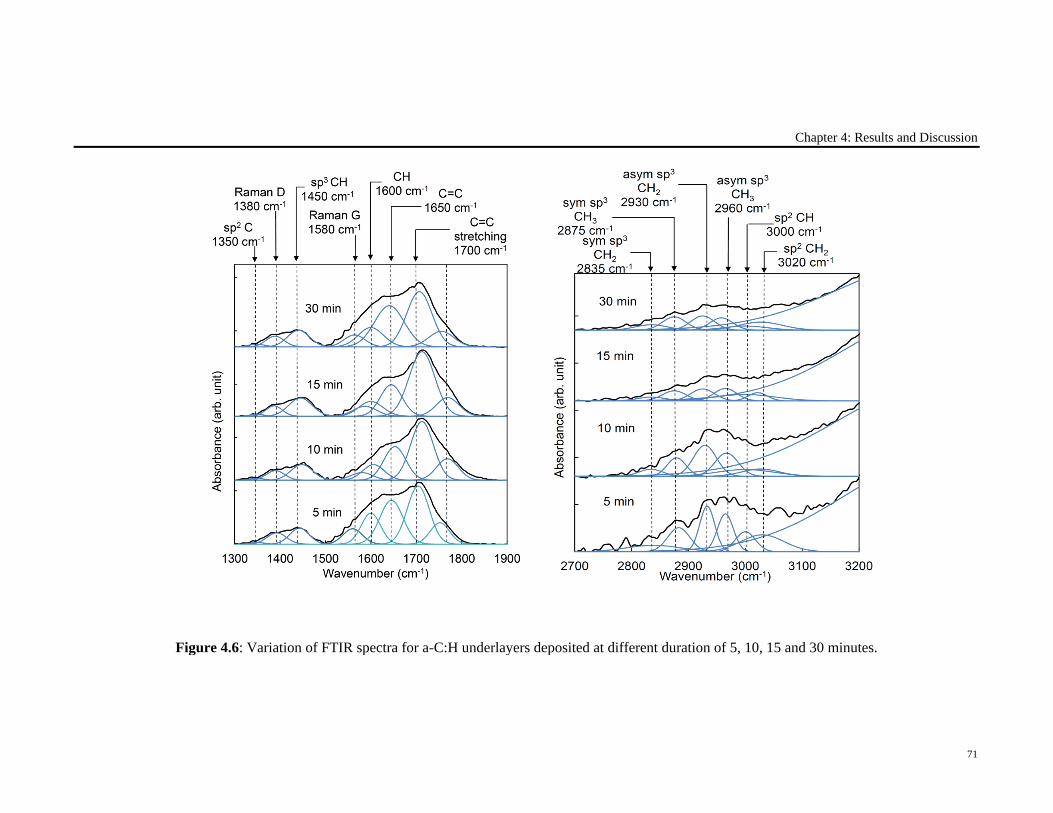
Chapter 4: Results and Discussion
71
Figure 4.6: Variation of FTIR spectra for a-C:H underlayers deposited at different duration of 5, 10, 15 and 30 minutes.
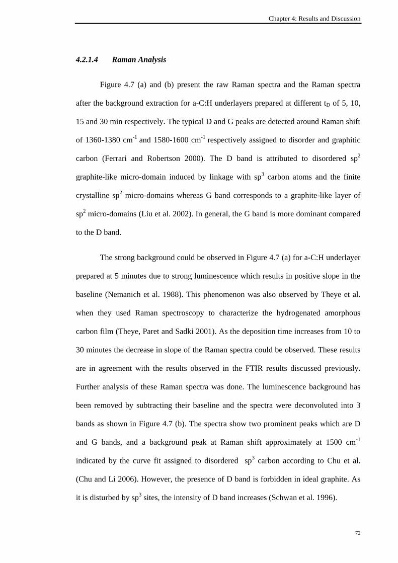
Chapter 4: Results and Discussion
72
4.2.1.4 Raman Analysis
Figure 4.7 (a) and (b) present the raw Raman spectra and the Raman spectra
after the background extraction for a-C:H underlayers prepared at different tD of 5, 10,
15 and 30 min respectively. The typical D and G peaks are detected around Raman shift
of 1360-1380 cm-1
and 1580-1600 cm-1
respectively assigned to disorder and graphitic
carbon (Ferrari and Robertson 2000). The D band is attributed to disordered sp2
graphite-like micro-domain induced by linkage with sp3 carbon atoms and the finite
crystalline sp2 micro-domains whereas G band corresponds to a graphite-like layer of
sp2 micro-domains (Liu et al. 2002). In general, the G band is more dominant compared
to the D band.
The strong background could be observed in Figure 4.7 (a) for a-C:H underlayer
prepared at 5 minutes due to strong luminescence which results in positive slope in the
baseline (Nemanich et al. 1988). This phenomenon was also observed by Theye et al.
when they used Raman spectroscopy to characterize the hydrogenated amorphous
carbon film (Theye, Paret and Sadki 2001). As the deposition time increases from 10 to
30 minutes the decrease in slope of the Raman spectra could be observed. These results
are in agreement with the results observed in the FTIR results discussed previously.
Further analysis of these Raman spectra was done. The luminescence background has
been removed by subtracting their baseline and the spectra were deconvoluted into 3
bands as shown in Figure 4.7 (b). The spectra show two prominent peaks which are D
and G bands, and a background peak at Raman shift approximately at 1500 cm-1
indicated by the curve fit assigned to disordered sp3 carbon according to Chu et al.
(Chu and Li 2006). However, the presence of D band is forbidden in ideal graphite. As
it is disturbed by sp3 sites, the intensity of D band increases (Schwan et al. 1996).
Chapter 4: Results and Discussion
73
Figure 4.7: The raw Raman spectra with strong background (a) and the Raman spectra after the background extraction (b)
for a-C:H underlayers prepared at different deposition duration of 5, 10, 15 and 30 min.
(a) (b) D D G G

Chapter 4: Results and Discussion
74
From Raman analysis, the variation of G and D peak positions, FWHM and
ID/ IG ratio for a-C:H underlayers as a function of tD were obtained as shown in Figure
4.8. In general, the G peak position is almost uniform at ~1590 cm-1
for all films as
shown in Figure 4.8 (a). This is higher than its 1550 cm-1
value in visible Raman but
does not exceed the band limit of graphitic carbon. This indicates that the shifted G peak
position in uv region is contributed by olefinic (chain) sp2 groups with high vibrational
frequencies than graphitic groups due to their shorter bond lengths (Gilkes et al. 1998) .
Likewise the D peak position, it is also uniform at around 1375 cm-1
for the a-C:H
underlayer deposited at tD of 5, 10 and 15 minutes and increases to 1390 cm-1
for a-C:H
underlayer prepared at tD of 30 minutes as shown in Figure 4.8 (b). The band width of G
and D bands for a-C:H underlayer prepared at tD of 10 minutes are highest compared to
others as seen in Figure 4.8 (c) and (d). It is suggested that the a-C:H underlayer
prepared at 10 minutes has lower degree of clustering of sp2
phases and less ordered
structures compared to those underlayers prepared at tD of 5, 15 and 30 minutes
(Jawhari, Roid and Casado 1995). This may be due to the increase in bond-angle
disorder at sp2 site in carbonaceous materials. From Figure 4.8 (e), the ID/IG ranges from
0.4 to 0.9. It is observed that the ID/IG decreases as the tD increases indicating an
increase in the ratio of sp3 to sp
2 bonded to carbon. Zhao et al has suggested that the low
ratio of ID/ IG (<1) in disordered graphite is due to the decrement of defect or ordering of
carbon atoms. This is shown by small crystal size or the destruction of symmetry in
crystallite structure (Zhao et al. 2011).

Chapter 4: Results and Discussion
75
Figure 4.8: Raman analysis of a-C:H underlayers prepared at tD of 5, 10, 15 and
30 minutes. Line is guide to the eyes.
(a) (b)
(c) (d)
(e)

Chapter 4: Results and Discussion
76
4.2.2 Effect on Resulting ns-CNx/a-C:H Formation
4.2.2.1 Surface and cross-sectional images
The surface and cross-sectional images of the ns-CNx deposited onto the a-C:H
underlayer which were produced at different tD are shown in Figure 4.9.
Surface Cross-sectional
(a) bare c-Si
(b) tD = 5 minutes
(c) tD = 10 minutes
(d) tD =15 minutes
(e) tD = 30 minutes
Figure 4.9: Surface and cross-sectional images of ns-CNx
deposited on a-C:H underlayer prepared at different tD.
1
1
1
1
1
1
1µ
1
1
1

Chapter 4: Results and Discussion
77
Figure 4.9 (a) shows that ns-CNx could be deposited directly on bare
c-Si substrate. These fiber-like nanostructures exhibited high aspect ratio with average
diameter of 88 ± 14 nm and length of 3.81 ± 0.09 μm. It was also observed from Figure
4.9 (b)-(e) that the formation of ns-CNx could be influenced by introducing the a-C:H as
an underlayer base. The formation of these ns-CNx on the a-C:H base varied in
accordance to tD. The nanostructures formed on the a-C:H underlayer deposited at tD of
5 minutes resembles those on bare c-Si substrate but the length of the former was
decreased by almost one third. Furthermore, they were more tightly packed and were
formed on the surface of the a-C:H underlayer. The film deposited on the a-C:H
underlayers at tD of 10 minutes were tightly packed, rigid and cylindrical in shape with
enhanced vertical alignment. These nanostructures show a slightly lower aspect ratio
compared to the fiber-like structures produced on the bare c-Si substrate whereby the
average diameter of the former was 84 ± 17 nm while their average length was
3.38 ± 0.07 m. The ns-CNx deposited on the a-C:H underlayer deposited at tD of
15 minutes formed bunches of dendrite-like structures fused at the base. The
nanostructures deposited on the a-C:H underlayer at tD of 30 minutes also showed a
dendrite-like structures but of smaller size protruding from that possibly the a-C:H
underlayer. This is influenced by cone-like structure of the a-C:H as underlayer appears
to decreases and disappear altogether.
Among these, the well aligned, rigid, cylindrical rod-like structure is of great
interest. Figure 4.10 compares the well aligned fiber-like CNx formed on bare c-Si and
a-C:H underlayer deposited at tD 10 minutes. The formation of the fiber-like ns-CNx
formed on the bare c-Si substrate is believed to be influenced by the crystalline structure
of the substrate itself. In contrast, this was not so for film grown on the c-Si substrate
coated with the a-C:H underlayer film. Here, the growth of the rod-like ns-CNx
coincided with the high surface roughness of the film. The high surface roughness was

Chapter 4: Results and Discussion
78
contributed by the presence of vertical broad tip cone-like features of the a-C:H
underlayer. These morphological features may have acted as the template for the
formation of these structures. Ion bombardments on the H terminated bonds of the cone-
like structures along with H etching effects during the growth of the CNx structures
might have induced the formation of a higher ordering of these structures which resulted
in the growth of highly aligned rigid cylindrical nanostructures. It is also seen that the
„roots‟ of the nanofibers that grew directly on the c-Si substrate appear to form
separately from each other. In contrast, the nanorods grew on the a-C:H underlayer
appears to have more solid base where their „roots‟ grew from. It is very likely that this
base is the a-C:H underlayer film.
For deposition on the a-C:H underlayers film which were produced at tD of 15
and 30 minutes, the formation of ns-CNx reduced significantly in size and appeared as
dendrite-like structures. These cone-like structures appear to be embedded in the a-C:H
film. The changes in the growth of the ns-CNx corresponds to the reduction in the
surface roughness of the a-C:H underlayer and shows that the growth of the nanorods
are effectively suppressed.
bare c-Si 10 minutes
Figure 4.10: Variation of FESEM cross-sectional images for ns-CNx deposited on
bare c-Si and 10 minutes a-C:H underlayer.
1 1

Chapter 4: Results and Discussion
79
4.2.2.2 Auger electron spectroscopy measurement of ns-CNx
The elemental composition of these ns-CNx was determined by using AES.
From these measurements the relative concentration (%) of C and N elements were
calculated. The N/C ratio for the ns-CNx grown on the a-C:H deposited as a function of
tD is shown in Figure 4.11. The results indicate that the incorporation of nitrogen was at
the highest for the film deposited at tD of 10 minutes. This coincides with the formation
of the rigid and aligned nanostructures (Ritikos et al. 2011). This indicates that high
incorporation of N atoms into the film structure is important in the formation of the
rigid and highly aligned vertical cylindrical ns-CNx. It is important to determine how
these N atoms are bonded to the C structure. This was studied by means of FTIR
characterization.
Figure 4.11: Variation of nitrogen to carbon N/C ratio of ns-CNx
deposited on c-Si, a-C:H underlayers at tD of 5, 10, 15 and 30 minutes.
0.1
0.12
0.14
0.16
0.18
0.2
0.22
0.24
0.26
0.28
0.3
0 10 20 30 40
N/C
ratio
Deposition time (min)
bare c-Si
Chapter 4: Results and Discussion
80
4.2.2.3 FTIR spectra of ns-CNx
The FTIR spectra obtained for the ns-CNx films deposited onto the a-C:H
underlayer which was prepared as a function of tD are shown in Figure 4.12. The
spectra are composed of 3 main characteristic bonding groups. These include the
absorption band at 1300-1800 cm-1
related to sp2-CH bending and C=C and/or C=N;
absorption band at 2000-2300 cm-1
corresponding to sp1
nitrile and/or isonitrile (CN)
bonds and those at 2800-3700 cm-1
which are related to sp3 CHn groups and N-H and /
or O-H (Motta and Pereyra 2004; Mutsukura and Akita 1999; Pereira et al. 2006). For
clarification, the individual spectra for each region are presented in Figure 4.13.
Compared to the spectra for the a-C:H underlayer (Figure 4.5), the spectra for the ns-
CNx films show the additional absorption region within the range of 2000-2300 cm-1
,
which was attributed to the incorporation of N atoms into the film structure. Indeed it is
the band in this region which shows the most significant changes with the variation in
the deposition parameter. These changes are deem more important and reliable than the
other regions since the changes in the sp2 or sp
3 phases may be influenced or
contributed by any changes in the a-C:H underlayer films during the CNx deposition.
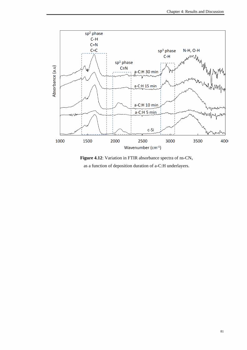
Chapter 4: Results and Discussion
81
Figure 4.12: Variation in FTIR absorbance spectra of ns-CNx
as a function of deposition duration of a-C:H underlayers.
H

Chapter 4: Results and Discussion
82
Figure 4.13: The FTIR spectra for ns-CNx deposited at different tD of a-C:H underlayers
in the range of (a) sp2, (b) sp1 and(c) sp3 phases.
(a) (b) (c)

Chapter 4: Results and Discussion
83
Figure 4.14: The FTIR spectra in the wavenumber range of 1900-2300 cm-1 of
CNx nanostructres as a function of tD a-C:H underlayers.
The spectra region in question, shown in Figure 4.14 is contributed by the
presence of nitrile and/or isonitrile (CN) bonds in the films. The broad bands in this
region were decomposed into five overlapping bands associated with these nitrile
(−C≡N) and isonitrile (−N≡C) bonds (Mutsukura 2001; Mutsukura and Akita 1999)
which include the isolated and/or fused aromatic rings bonded either to isonitrile
(−N≡C) bonds at 2105 cm-1
or nitrile bonds (−C≡N) at 2215 cm-1
; hydrocarbon
molecules which include C2H5 at 2160 cm-1
and CH3 at 2190 cm-1
bonded to isonitrile
(−N≡C); and the hydrocarbon groups (CH3, C2H5, etc.) bonded to nitrile (−C≡N) which
appear as a single peak at 2245 cm-1
. The deconvolution of the spectra carried out using
standard Gaussian curve-fitting method (Fanchini et al. 2005; Mutsukura and Akita
1999) is shown in Figure 4.15. Among these spectra and their deconvolution, a
consistency in the film prepared on bare c-Si and the underlayer film at tD of 10 minutes
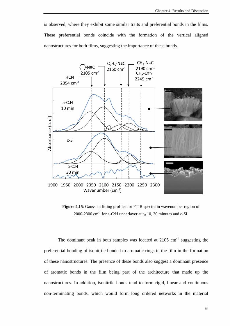
Chapter 4: Results and Discussion
84
is observed, where they exhibit some similar traits and preferential bonds in the films.
These preferential bonds coincide with the formation of the vertical aligned
nanostructures for both films, suggesting the importance of these bonds.
Figure 4.15: Gaussian fitting profiles for FTIR spectra in wavenumber region of
2000-2300 cm-1 for a-C:H underlayer at tD 10, 30 minutes and c-Si.
The dominant peak in both samples was located at 2105 cm-1
suggesting the
preferential bonding of isonitrile bonded to aromatic rings in the film in the formation
of these nanostructures. The presence of these bonds also suggest a dominant presence
of aromatic bonds in the film being part of the architecture that made up the
nanostructures. In addition, isonitrile bonds tend to form rigid, linear and continuous
non-terminating bonds, which would form long ordered networks in the material

Chapter 4: Results and Discussion
85
suitable for the formation of the nanostructured fibers and rods. Furthermore,
preferential bonding of the ring through N atom rather than C for the isonitrile,
suggested the presence of partial charge (−N+≡C
−) formed within the nanostructures.
The electric field imposed by the RF plasma aligns the partial charge, resulting in the
formation of the vertical aligned growth of these structures perpendicular to substrate
surface (Ritikos et al. 2011).
4.2.3 Summary
The influence of the surface morphological and chemical bonding properties of
PECVD-grown a-C:H underlayer pre-deposited films on p-type <111> c-Si substrates
were studied. The effects of the films properties on the subsequent growth ns-CNx
produced on these films are reported. This study shows that a-C:H pre-deposited
underlayer films could be used as a template for the formation and modification of ns-
CNx. Indeed with the use of these a-C:H template the rigidity and shape of the ns-CNx
could be modified from the vertically aligned CNx nanorods produced on bare c-Si. The
formation of rigid and vertically aligned cylindrical ns-CNx is produced on a-C:H
underlayer prepared at tD of 10 minutes. Though the structure and properties of these
a-C:H films appear to have minimal variation with tD, the a-C:H film produced at tD of
10 minutes shows the highest surface roughness. Its surface morphology is made up of
broad tip cone-like structures with highly ordered sp2 clusters covered with H
terminated bond. Nitrogen incorporation in ns-CNx and the preference of isonitrile
bonds in the film induce the formation of vertically aligned ns-CNx.

Chapter 4: Results and Discussion
86
4.3 Effects of RF Power on a-C:H Underlayer and Resulting CNx/a-C:H
Formation
This section study the effects of different applied RF power, PUL on the
deposition of the a-C:H underlayer and the effects on the resulting ns-CNx. PUL were set
at 30, 40, 50, 60, 80 and 100 W giving 6 sets of a-C:H underlayers and corresponding
ns-CNx/a-C:H films. The deposition time was fixed at 10 minutes. The effects of
applied RF power on the formation of a-C:H underlayers by RFPECVD have been
investigated by other researchers working on this material (Choi et al. 2005; von
Keudell, Meier and Hopf 2002). It is generally accepted that applied power significantly
influences the structure of the deposited a-C:H films. Three aspects are usually taken
into consideration when dealing with the studies of PUL on the film deposition. These
include (i) the dissociation of gas precursors through primary and secondary reactions in
the plasma, (ii) absorption and desorption processes on the film surface, and (iii) ion
bombardment on the growth surface. The first aspect is associated with gas phase
reactions, while the second and third aspects are related to surface reactions. Each
aspect has its influence on the resulting film.
4.3.1 Effects of RF Power on a-C:H Underlayer
4.3.1.1 Growth rate of a-C:H underlayers
Figure 4.16 shows the relationship between PUL and the corresponding film
growth rate of the a-C:H underlayers. It is also found that the increase in PUL
significantly increases the growth rate of the a-C:H underlayer films. The reason for the
increase in growth rate is probably due to the increase in dissociation of the CH4. This
will increase the number of reactive species in the plasma including hydrocarbon radical
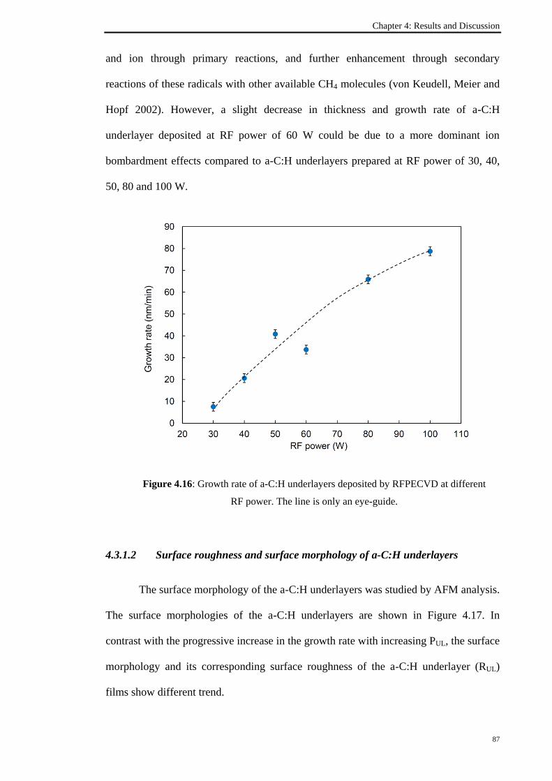
Chapter 4: Results and Discussion
87
and ion through primary reactions, and further enhancement through secondary
reactions of these radicals with other available CH4 molecules (von Keudell, Meier and
Hopf 2002). However, a slight decrease in thickness and growth rate of a-C:H
underlayer deposited at RF power of 60 W could be due to a more dominant ion
bombardment effects compared to a-C:H underlayers prepared at RF power of 30, 40,
50, 80 and 100 W.
Figure 4.16: Growth rate of a-C:H underlayers deposited by RFPECVD at different
RF power. The line is only an eye-guide.
4.3.1.2 Surface roughness and surface morphology of a-C:H underlayers
The surface morphology of the a-C:H underlayers was studied by AFM analysis.
The surface morphologies of the a-C:H underlayers are shown in Figure 4.17. In
contrast with the progressive increase in the growth rate with increasing PUL, the surface
morphology and its corresponding surface roughness of the a-C:H underlayer (RUL)
films show different trend.

Chapter 4: Results and Discussion
88
Figure 4.17: AFM surface morphology of a-C:H underlayers deposited for RF power
of 30, 40, 50, 60, 80 and 100 W.
Figure 4.18 presents the variation of surface roughness RUL of a-C:H
underlayers as a function of PUL . RUL was almost constant when PUL is varied from 30
to 50 W, then spikes to a maximum at PUL of 60 W before decreasing to a minimum at
PUL of 80 W. With the current results, specific explanations could not be given for the
variation in RUL with PUL particularly to the significant decrease in RUL for film
deposited at PUL of 80 W. However, the changes in RUL are believed to be attributed by
various degree and contribution of the gas phase and surface reactions. Though the
substrate is grounded throughout the deposition process, ion bombardment contributed
by the plasma, is expected to play an important role in the structural formation of the
films. This may be true considering the close proximity of the electrodes (1 cm). Ion
bombardment would effectively remove weak hydrogen bonds from the surface
allowing structural modifications to occur as PUL is varied. Also when PUL is increased,
primary reactions would dominate the gas phase reactions allowing increase in
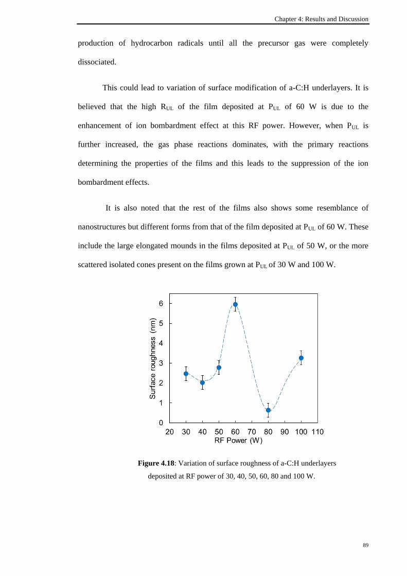
Chapter 4: Results and Discussion
89
production of hydrocarbon radicals until all the precursor gas were completely
dissociated.
This could lead to variation of surface modification of a-C:H underlayers. It is
believed that the high RUL of the film deposited at PUL of 60 W is due to the
enhancement of ion bombardment effect at this RF power. However, when PUL is
further increased, the gas phase reactions dominates, with the primary reactions
determining the properties of the films and this leads to the suppression of the ion
bombardment effects.
It is also noted that the rest of the films also shows some resemblance of
nanostructures but different forms from that of the film deposited at PUL of 60 W. These
include the large elongated mounds in the films deposited at PUL of 50 W, or the more
scattered isolated cones present on the films grown at PUL of 30 W and 100 W.
Figure 4.18: Variation of surface roughness of a-C:H underlayers
deposited at RF power of 30, 40, 50, 60, 80 and 100 W.

Chapter 4: Results and Discussion
90
4.3.1.3 FTIR spectra of a-C:H underlayers
The FTIR spectra of the C:H underlayer films prepared at different PUL are
shown in Figure 4.19. Included is also the corresponding surface roughness. These
spectra also show the expected functional groups common for a-C:H films. These
groups consist of various sp2 C related bonds in the wave number range of
1300-1700 cm-1
. Among others, these bonds include those of CC, the so called G and
D bands and sp2 C bonds at frequency range of, 1550-1570 cm
-1, 1360-1380 cm
-1 and
1620-1650 cm-1
, respectively (Lazar et al. 2005). Also, the CHn bands are clearly
observed within the frequency range of 2800-3050 cm-1
which includes various
overlapping sp2 and sp
3 CHn bonds (Ghodselahi and Vesaghi 2008). For clarification,
the individual spectra for each region are presented in Figure 4.20.
A significant difference between the spectra of the film deposited at PUL of 60 W
and the rest of the films is clearly seen and this film shows the highest RUL. While the
rest of the films show a more dominant and stronger CHn bands than the sp2
C bands,
the opposite is seen for film at PUL of 60 W. The decrease in CHn shows that there is a
significant decrease in H content in the film. This is in line with the proposed decrease
of H bonds due to their removal by ion bombardment. The sp2 C bonds are observed to
show a more dominant presence in these films compared to sp3 C bonds. The clustering
of sp2 C species within the amorphous sp
3 C matrix is reflected by the surface
morphology and high RUL of the film deposited at RF power of 60 W. The smooth cone
shaped structures seen on the film deposited at PUL of 60 W, may very well be linked to
these sp2 clusters. On the other hand with further increase in PUL to 80 W and 100 W,
the increase in the H content supports the later explanation of decrease in surface
roughness in AFM analysis attributed to the suppression of ion bombardment effect on
the film during growth. Indeed in both extreme cases of the films deposited at PUL of 60
W and 80 W, where the former show the highest RUL but weakest CHn bonds (high sp2
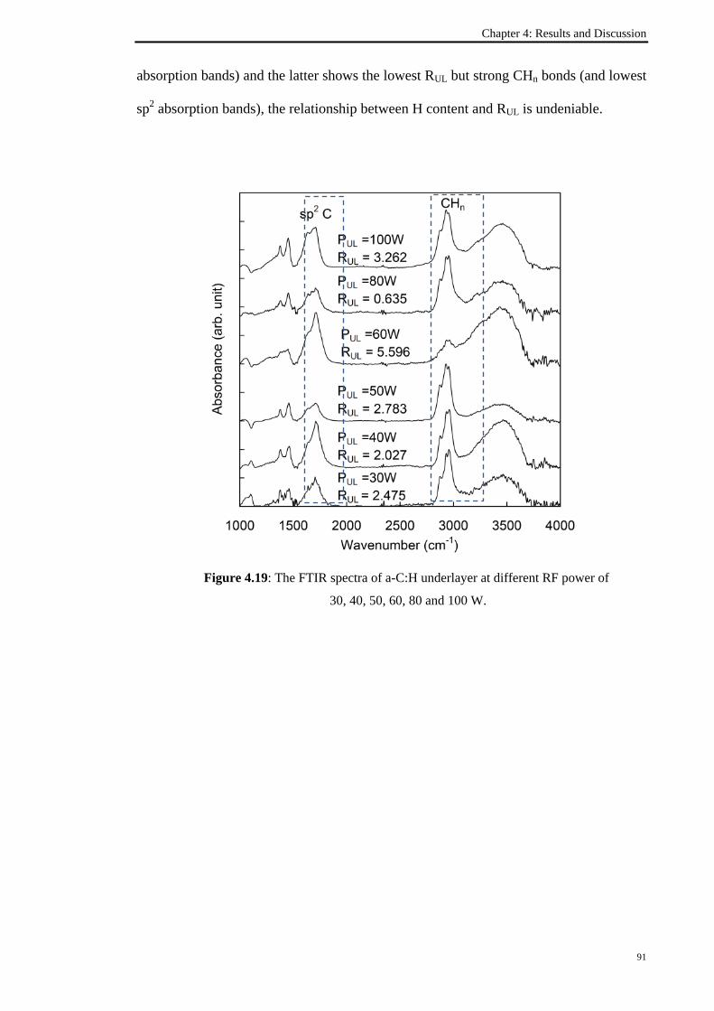
Chapter 4: Results and Discussion
91
absorption bands) and the latter shows the lowest RUL but strong CHn bonds (and lowest
sp2 absorption bands), the relationship between H content and RUL is undeniable.
Figure 4.19: The FTIR spectra of a-C:H underlayer at different RF power of
30, 40, 50, 60, 80 and 100 W.

Chapter 4: Results and Discussion
92
Figure 4.20: Variation of FTIR spectra for a-C:H underlayers deposited at
different RF power in the range of 1400-2000 cm-1 and 2600-4000 cm-1.
4.3.1.4 Raman scattering analysis
The structural properties of a-C:H underlayers was further studied by Raman
scattering microscopy. The Raman spectra of a-C:H underlayers deposited at different
PUL are shown in Figure 4.21. Figure 4.21 (a) is plotted from the raw Raman data and
exhibits strong photoluminescence (PL) background which causes the positive slope in
the spectral baseline. The presence of this slope was also observed by Casiraghi et al. in
their study of hydrogenated diamond-like carbon films (Casiraghi et al. 2005).
According to Casiraghi et al., the increasing PL background is due to increasing H
content in the films which contributes to hydrogen saturation of non-radiative
recombination centers in the films (Escobar-Alarcón et al. 2005).
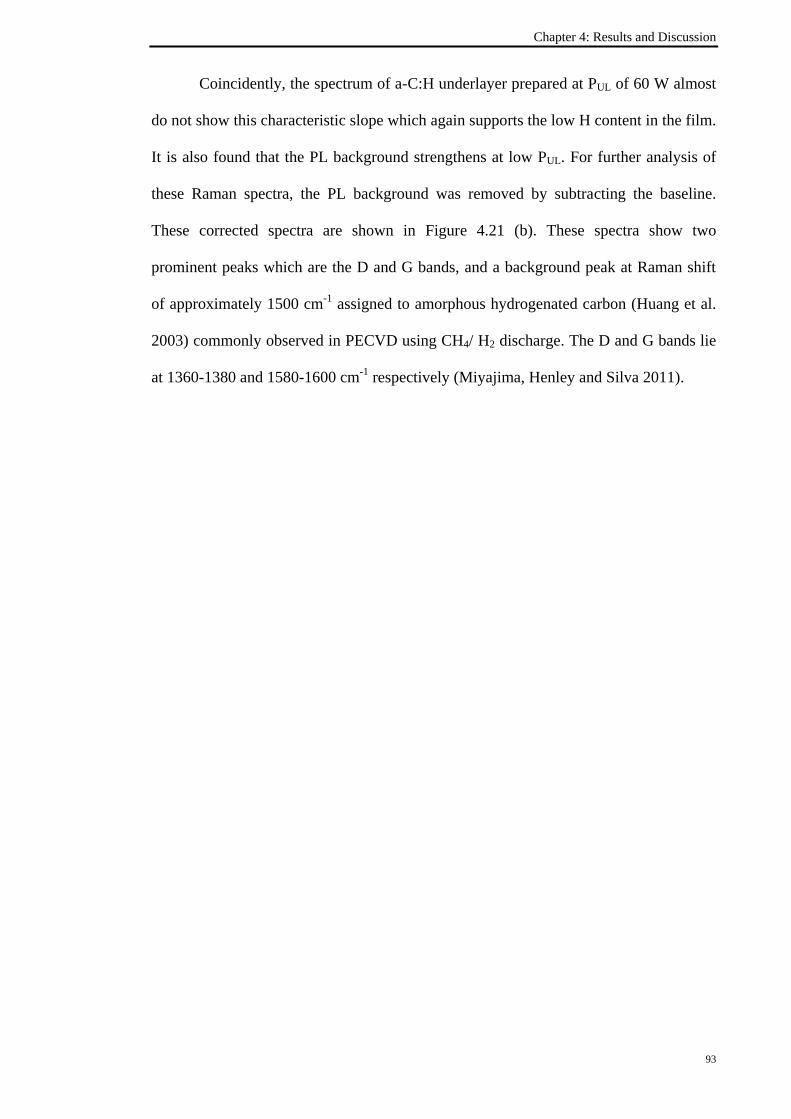
Chapter 4: Results and Discussion
93
Coincidently, the spectrum of a-C:H underlayer prepared at PUL of 60 W almost
do not show this characteristic slope which again supports the low H content in the film.
It is also found that the PL background strengthens at low PUL. For further analysis of
these Raman spectra, the PL background was removed by subtracting the baseline.
These corrected spectra are shown in Figure 4.21 (b). These spectra show two
prominent peaks which are the D and G bands, and a background peak at Raman shift
of approximately 1500 cm-1
assigned to amorphous hydrogenated carbon (Huang et al.
2003) commonly observed in PECVD using CH4/ H2 discharge. The D and G bands lie
at 1360-1380 and 1580-1600 cm-1
respectively (Miyajima, Henley and Silva 2011).
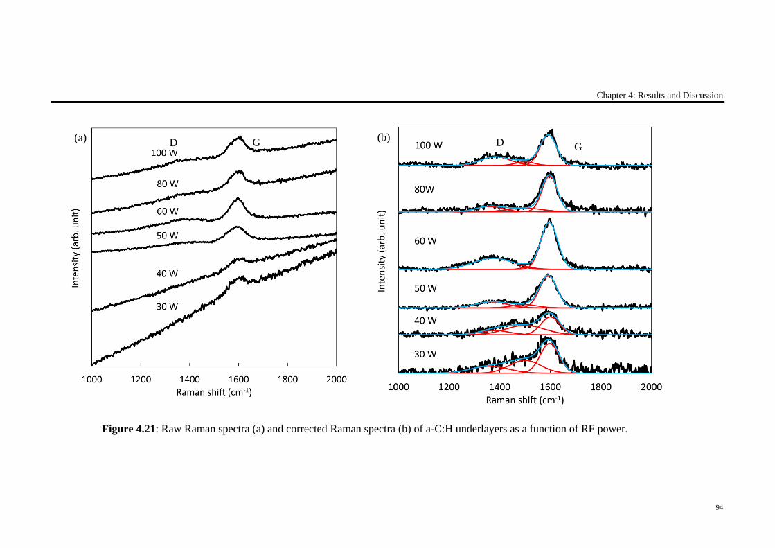
Chapter 4: Results and Discussion
94
Figure 4.21: Raw Raman spectra (a) and corrected Raman spectra (b) of a-C:H underlayers as a function of RF power.
(a) (b) D G D G

Chapter 4: Results and Discussion
95
Figure 4.22 presents the Raman analysis of a-C:H underlayers including the
variation in (a) G peak position, (b) D peak position, (c) FWHMG, (d) FWHMD and
(e) ID/IG. In general the G peak positions of all these films were blue shifted towards
1600 cm-1
compared to deposition normally found for pure graphite at 1560 cm-1
. This
indicates that these films are made up not only of nanocrytalline graphitic structure but
also C=C sp2 stretching vibrations of olefinic or conjugated carbon “chain” in the films
(Schwan et al. 1996; Wang and Zhang 2007). As shown in Figure 4.22 (d), a-C:H
underlayer films prepared at 30 and 60 W show higher FWHMD compared to the rest of
the films. This behavior indicates increase in the disorder in sp2 C bonds. This is due to
the presence of different order in the clusters distribution.
Among these films, the a-C:H underlayers deposited at 60 and 100 W shows
high ID/IG ratio of 0.56 and 0.52, respectively. High in ID/IG indicates an increase in the
number and/or size of graphitic cluster in the films (Ferrari and Robertson 2000). This
suggests that the C atoms have high probability of forming C=C ring structures rather
than the chain structure. In addition, a-C:H underlayer prepared at PUL of 60 W has the
highest ID/IG ratio which is ascribed to the conversion of sp3 to sp
2 bonds and
desorption of hydrogen. This is also in line with FTIR results which show more sp2 C
bonds. Thus, the a-C:H underlayer film prepared at PUL of 60 W has dominant sp2 C
bonds. The Raman results suggest that the a-C:H underlayer deposited at PUL of 60 W
consists of dominant sp2 clusters compared to the rest of the films. This supported the
observation in both AFM and surface roughness results that these sp2 clusters may
contribute to highest surface roughness seen in the film.
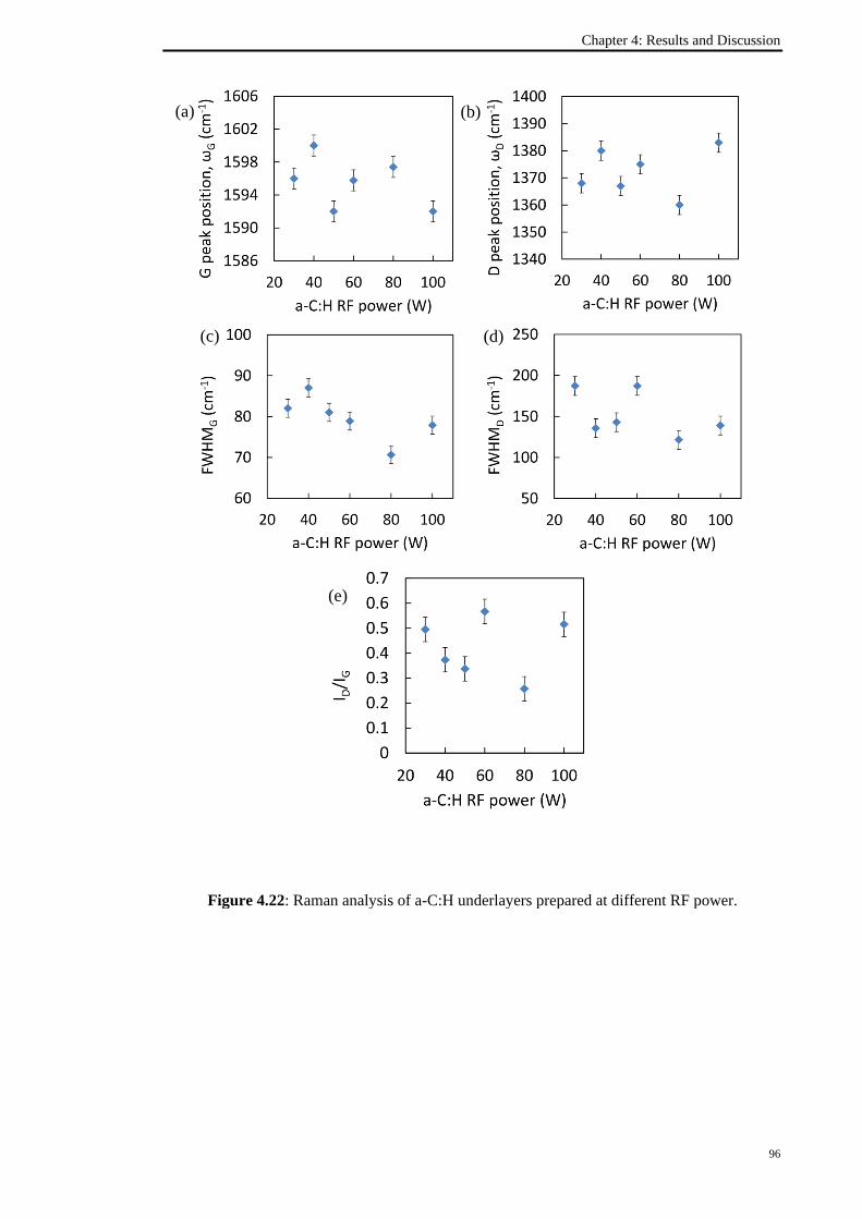
Chapter 4: Results and Discussion
96
Figure 4.22: Raman analysis of a-C:H underlayers prepared at different RF power.
(a) (b)
(c) (d)
(e)
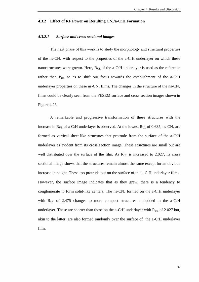
Chapter 4: Results and Discussion
97
4.3.2 Effect of RF Power on Resulting CNx/a-C:H Formation
4.3.2.1 Surface and cross-sectional images
The next phase of this work is to study the morphology and structural properties
of the ns-CNx with respect to the properties of the a-C:H underlayer on which these
nanostructures were grown. Here, RUL of the a-C:H underlayer is used as the reference
rather than PUL so as to shift our focus towards the establishment of the a-C:H
underlayer properties on these ns-CNx films. The changes in the structure of the ns-CNx
films could be clearly seen from the FESEM surface and cross section images shown in
Figure 4.23.
A remarkable and progressive transformation of these structures with the
increase in RUL of a-C:H underlayer is observed. At the lowest RUL of 0.635, ns-CNx are
formed as vertical sheet-like structures that protrude from the surface of the a-C:H
underlayer as evident from its cross section image. These structures are small but are
well distributed over the surface of the film. As RUL is increased to 2.027, its cross
sectional image shows that the structures remain almost the same except for an obvious
increase in height. These too protrude out on the surface of the a-C:H underlayer films.
However, the surface image indicates that as they grew, there is a tendency to
conglomerate to form solid-like centers. The ns-CNx formed on the a-C:H underlayer
with RUL of 2.475 changes to more compact structures embedded in the a-C:H
underlayer. These are shorter than those on the a-C:H underlayer with RUL of 2.027 but,
akin to the latter, are also formed randomly over the surface of the a-C:H underlayer
film.
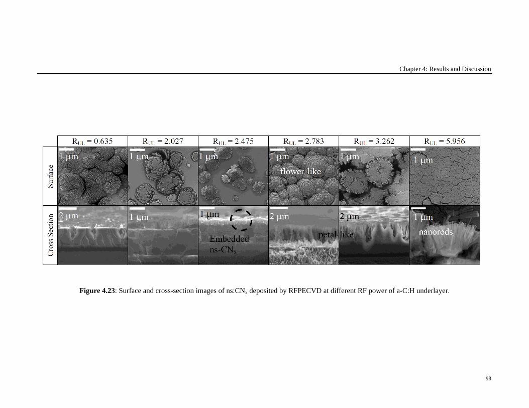
Chapter 4: Results and Discussion
98
Figure 4.23: Surface and cross-section images of ns:CNx deposited by RFPECVD at different RF power of a-C:H underlayer.
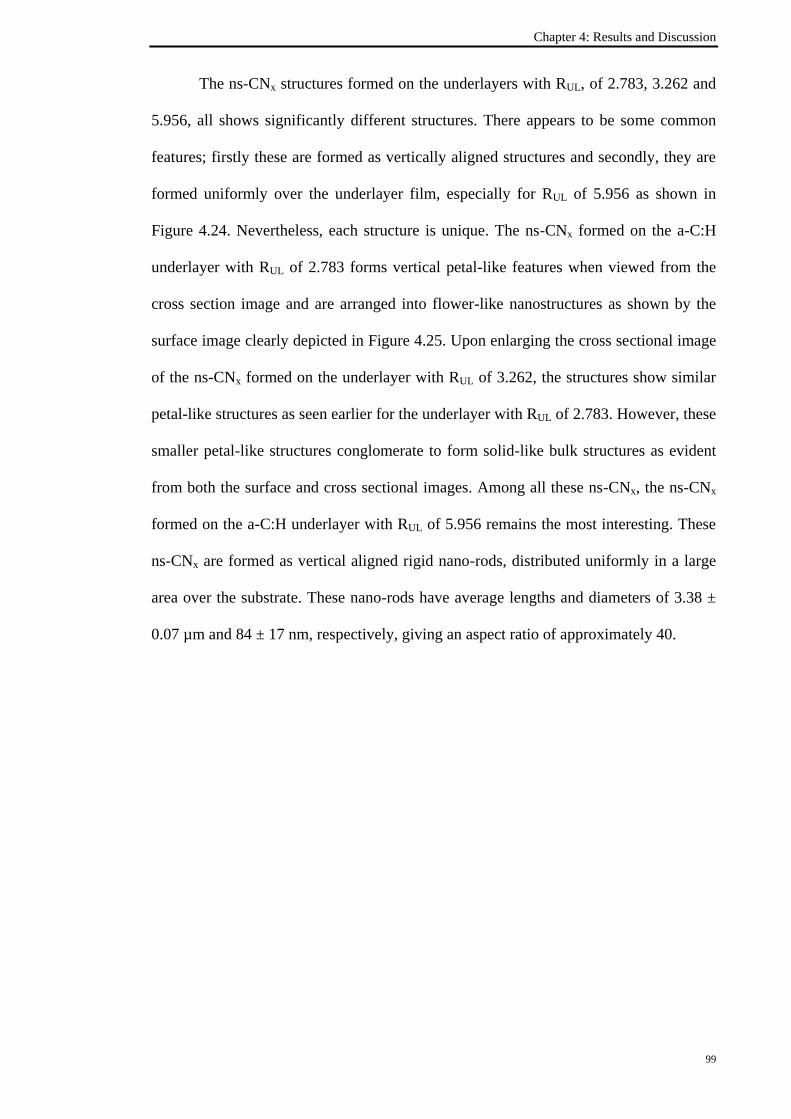
Chapter 4: Results and Discussion
99
The ns-CNx structures formed on the underlayers with RUL, of 2.783, 3.262 and
5.956, all shows significantly different structures. There appears to be some common
features; firstly these are formed as vertically aligned structures and secondly, they are
formed uniformly over the underlayer film, especially for RUL of 5.956 as shown in
Figure 4.24. Nevertheless, each structure is unique. The ns-CNx formed on the a-C:H
underlayer with RUL of 2.783 forms vertical petal-like features when viewed from the
cross section image and are arranged into flower-like nanostructures as shown by the
surface image clearly depicted in Figure 4.25. Upon enlarging the cross sectional image
of the ns-CNx formed on the underlayer with RUL of 3.262, the structures show similar
petal-like structures as seen earlier for the underlayer with RUL of 2.783. However, these
smaller petal-like structures conglomerate to form solid-like bulk structures as evident
from both the surface and cross sectional images. Among all these ns-CNx, the ns-CNx
formed on the a-C:H underlayer with RUL of 5.956 remains the most interesting. These
ns-CNx are formed as vertical aligned rigid nano-rods, distributed uniformly in a large
area over the substrate. These nano-rods have average lengths and diameters of 3.38 ±
0.07 µm and 84 ± 17 nm, respectively, giving an aspect ratio of approximately 40.
Chapter 4: Results and Discussion
100
Figure 4.24: FESEM cross section image for ns-CNx deposited on
pre-deposited a-C:H underlayer with surface roughness of 5.956.
4.3.2.2 Auger electron spectroscopy measurement of CNx nanostructures
AES analysis was done to determine the chemical composition of C and N in
these ns-CNx. Figure 4.26 presents the variation of N/C ratio as a function of RUL. This
1
1
Figure 4.25: FESEM surface image for ns-CNx deposited
on pre-deposited a-C:H underlayer with surface roughness of 2.783.
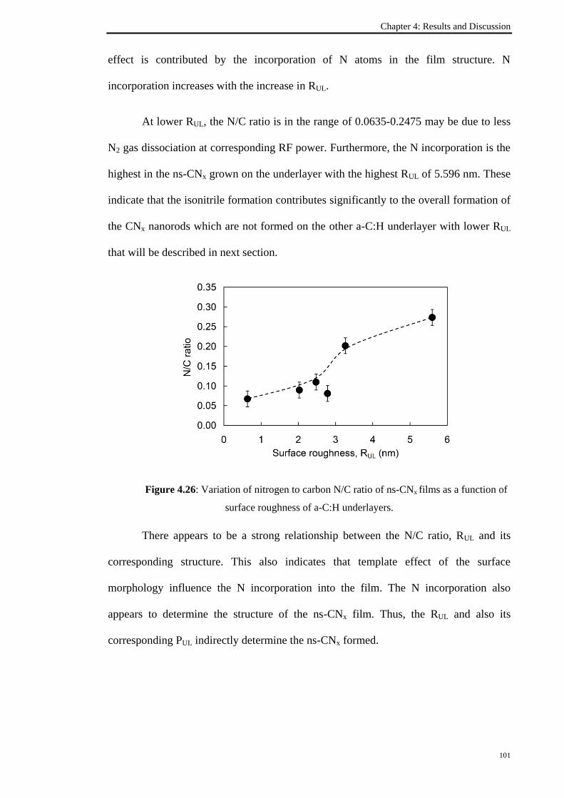
Chapter 4: Results and Discussion
101
effect is contributed by the incorporation of N atoms in the film structure. N
incorporation increases with the increase in RUL.
At lower RUL, the N/C ratio is in the range of 0.0635-0.2475 may be due to less
N2 gas dissociation at corresponding RF power. Furthermore, the N incorporation is the
highest in the ns-CNx grown on the underlayer with the highest RUL of 5.596 nm. These
indicate that the isonitrile formation contributes significantly to the overall formation of
the CNx nanorods which are not formed on the other a-C:H underlayer with lower RUL
that will be described in next section.
Figure 4.26: Variation of nitrogen to carbon N/C ratio of ns-CNx films as a function of
surface roughness of a-C:H underlayers.
There appears to be a strong relationship between the N/C ratio, RUL and its
corresponding structure. This also indicates that template effect of the surface
morphology influence the N incorporation into the film. The N incorporation also
appears to determine the structure of the ns-CNx film. Thus, the RUL and also its
corresponding PUL indirectly determine the ns-CNx formed.
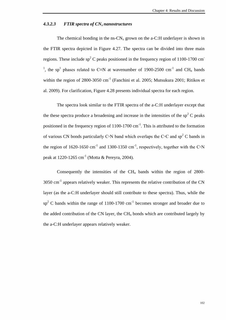
Chapter 4: Results and Discussion
102
4.3.2.3 FTIR spectra of CNx nanostructures
The chemical bonding in the ns-CNx grown on the a-C:H underlayer is shown in
the FTIR spectra depicted in Figure 4.27. The spectra can be divided into three main
regions. These include sp2 C peaks positioned in the frequency region of 1100-1700 cm
-
1, the sp
1 phases related to C≡N at wavenumber of 1900-2500 cm
-1 and CHn bands
within the region of 2800-3050 cm-1
(Fanchini et al. 2005; Mutsukura 2001; Ritikos et
al. 2009). For clarification, Figure 4.28 presents individual spectra for each region.
The spectra look similar to the FTIR spectra of the a-C:H underlayer except that
the these spectra produce a broadening and increase in the intensities of the sp2 C peaks
positioned in the frequency region of 1100-1700 cm-1
. This is attributed to the formation
of various CN bonds particularly C꞊N band which overlaps the C꞊C and sp2 C bands in
the region of 1620-1650 cm-1
and 1300-1350 cm-1
, respectively, together with the C꞊N
peak at 1220-1265 cm-1
(Motta & Pereyra, 2004).
Consequently the intensities of the CHn bands within the region of 2800-
3050 cm-1
appears relatively weaker. This represents the relative contribution of the CN
layer (as the a-C:H underlayer should still contribute to these spectra). Thus, while the
sp2 C bands within the range of 1100-1700 cm
-1 becomes stronger and broader due to
the added contribution of the CN layer, the CHn bonds which are contributed largely by
the a-C:H underlayer appears relatively weaker.
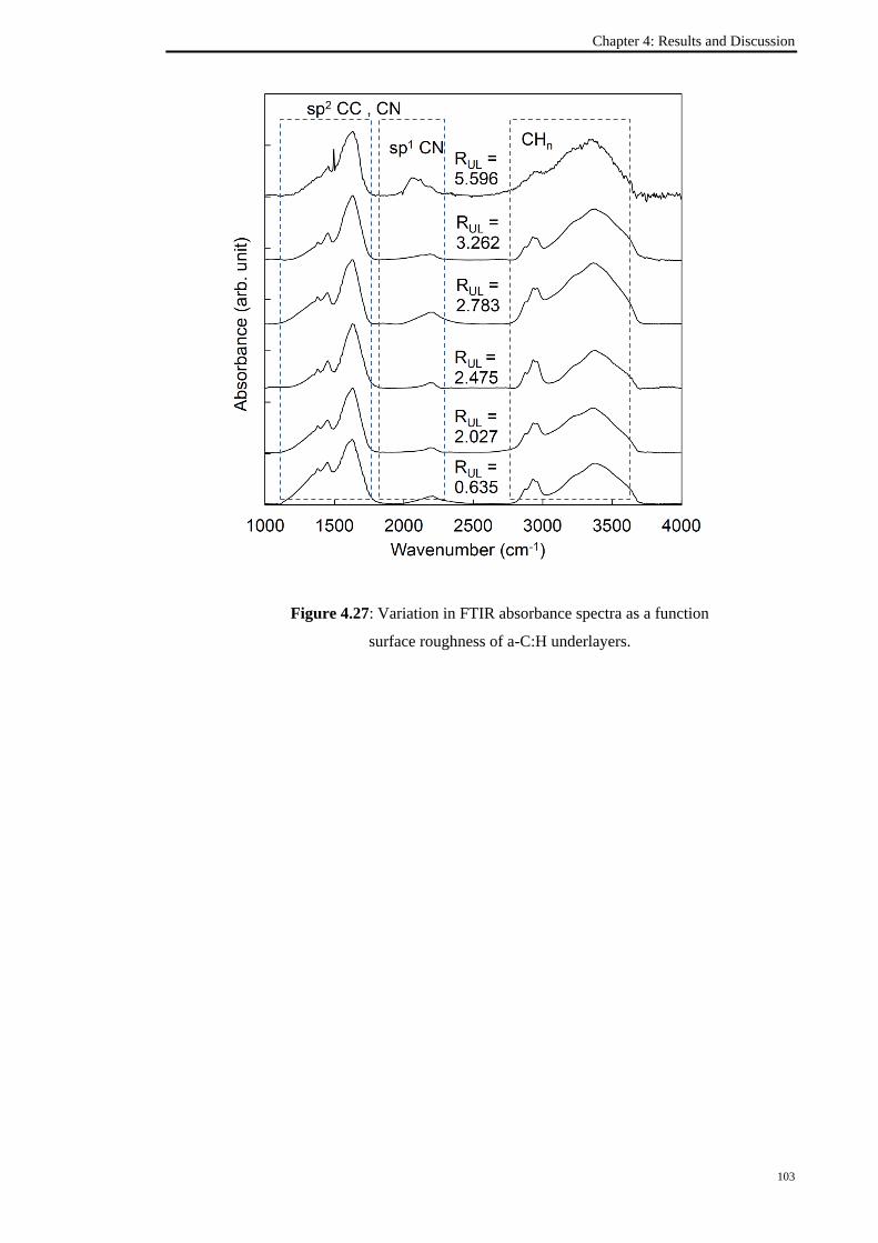
Chapter 4: Results and Discussion
103
Figure 4.27: Variation in FTIR absorbance spectra as a function
surface roughness of a-C:H underlayers.
Chapter 4: Results and Discussion
104
Figure 4.28: The FTIR spectra for CNx nanostructures deposited on a-C:H underlayers with different roughness
in the range of (a) sp2, (b) sp1 and (c) sp3 phases.
(a) (b) (c)
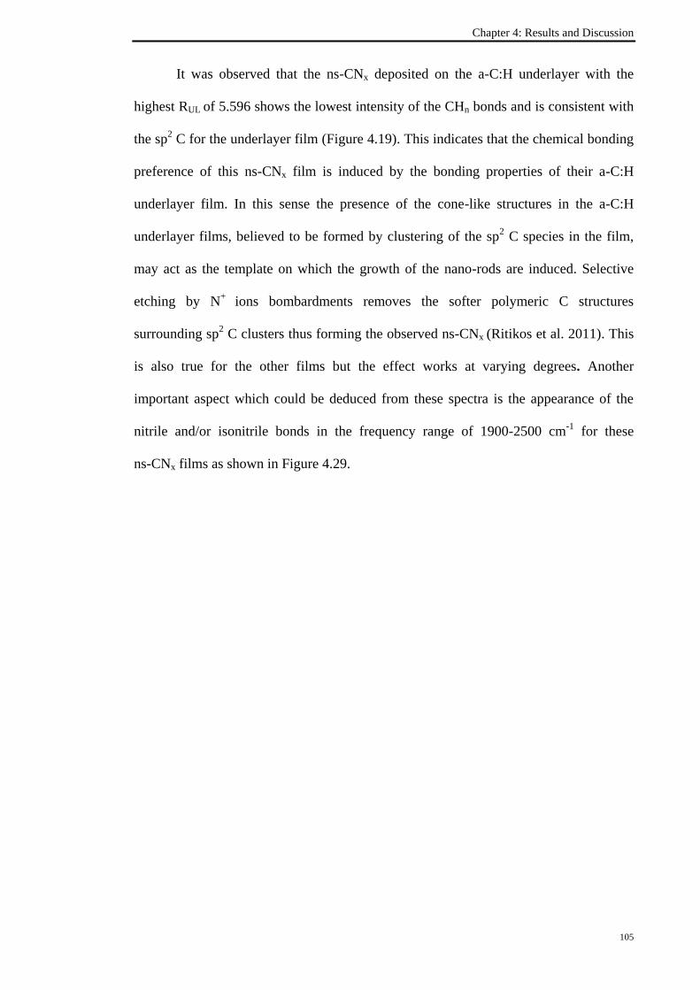
Chapter 4: Results and Discussion
105
It was observed that the ns-CNx deposited on the a-C:H underlayer with the
highest RUL of 5.596 shows the lowest intensity of the CHn bonds and is consistent with
the sp2 C for the underlayer film (Figure 4.19). This indicates that the chemical bonding
preference of this ns-CNx film is induced by the bonding properties of their a-C:H
underlayer film. In this sense the presence of the cone-like structures in the a-C:H
underlayer films, believed to be formed by clustering of the sp2 C species in the film,
may act as the template on which the growth of the nano-rods are induced. Selective
etching by N+
ions bombardments removes the softer polymeric C structures
surrounding sp2 C clusters thus forming the observed ns-CNx (Ritikos et al. 2011). This
is also true for the other films but the effect works at varying degrees. Another
important aspect which could be deduced from these spectra is the appearance of the
nitrile and/or isonitrile bonds in the frequency range of 1900-2500 cm-1
for these
ns-CNx films as shown in Figure 4.29.

Chapter 4: Results and Discussion
106
Figure 4.29: The FTIR spectra in the range of 1900-2300 cm-1 of ns-CNx
as a function of RUL a-C:H underlayers.
The band superposes isolated and/or fused aromatic rings bonded either to
isonitrile (-N≡C) at 2105 cm-1
or nitrile (-C≡N) at 2215 cm-1
, hydrocarbon molecules
which includes C2H5 at 2160 cm-1
and CH3 at 2190 cm-1
bonded to isonitrile (N≡C), and
hydrocarbon groups (CH3, C2H5, etc.) bonded to nitrile (-C≡N) located as a single peak
at 2245 cm-1
(Mutsukura and Akita 1999). Generally, the CNx films deposited on the
a-C:H underlayer films with RUL in the range of 0.63-3.26 nm show a dominant peak
attributed to isonitrile bonded to aliphatic at approximately 2190 cm-1
. In contrast, the
nanorods shows preferential formation of isonitriles bonded to aromatic rings at 2105
cm-1
. The differences is seen in the formation of aromatic rings attributed by the
increase in sp2 C bonds in the a-C:H films and CNx nanorods. From our previous
studies, we also deduce that isonitrile bonds induce a partial charge within these
nanostructures, and together with the electric field imposed by the RF plasma results in
the vertical alignment. Figure 4.30 shows the example of Gausian fitting related to those
Chapter 4: Results and Discussion
107
bonds in the region of 2000-2300 cm-1
for a-C:H underlayers with surface roughness of
5.596 and 3.262.
Figure 4.30: Gaussian fitting profiles for FTIR spectra in the region 2000-2300 cm-1 for a-C:H
underlayers with surface roughness 5.596 and 3.262.
4.3.3 Summary
The effects of RF power on the growth rate, surface morphology and chemical
bonding of the a-C:H underlayer film have been studied. Consequently, the morphology
and structural properties of ns-CNx film formed on these underlayer film were
investigated. The RF power indirectly determines the formation of the sp2 C clusters
and surface morphology of the a-C:H underlayer. The variation in surface roughness
and morphology of the a-C:H underlayer result in the formation of ns-CNx with unique
features such as flower-like structures and vertically aligned rigid nano-rods. The sp2 C

Chapter 4: Results and Discussion
108
clusters in the a-C:H underlayer acted as templates, where selective etching of the softer
polymeric C structures surrounding or within the clusters by N+ ion bombardment in the
different ns-CNx on the a-C:H underlayers occured. High N incorporation and the
preferential formation of isonitrile bonds is the condition that forms vertically aligned
rigid carbon nitride nanostructures.
4.4 Effects of Hydrogen Treatment on the a-C:H Underlayer and the Resulting
CNx/ a-C:H Film
The third part of the study emphasize the effects of different time duration of H2
plasma treatment on the a-C:H underlayers, deposited for 10 minutes and at RF power
of 100 W, also on the properties of the resulting CNx/a-C:H nanostructures. There are 4
sets of sample including the as-deposited a-C:H underlayer (without H2 plasma
treatment), 3, 5 and 10 minutes treated a-C:H underlayers and their corresponding CNx
films. The surface morphology, chemical, structural and elemental composition
properties of the films were studied.
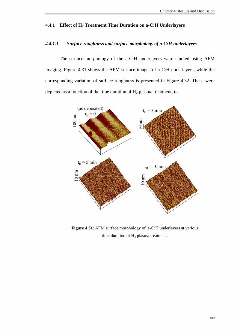
Chapter 4: Results and Discussion
109
4.4.1 Effect of H2 Treatment Time Duration on a-C:H Underlayers
4.4.1.1 Surface roughness and surface morphology of a-C:H underlayers
The surface morphology of the a-C:H underlayers were studied using AFM
imaging. Figure 4.31 shows the AFM surface images of a-C:H underlayers, while the
corresponding variation of surface roughness is presented in Figure 4.32. These were
depicted as a function of the time duration of H2 plasma treatment, tH.
Figure 4.31: AFM surface morphology of a-C:H underlayers at various
time duration of H2 plasma treatment.
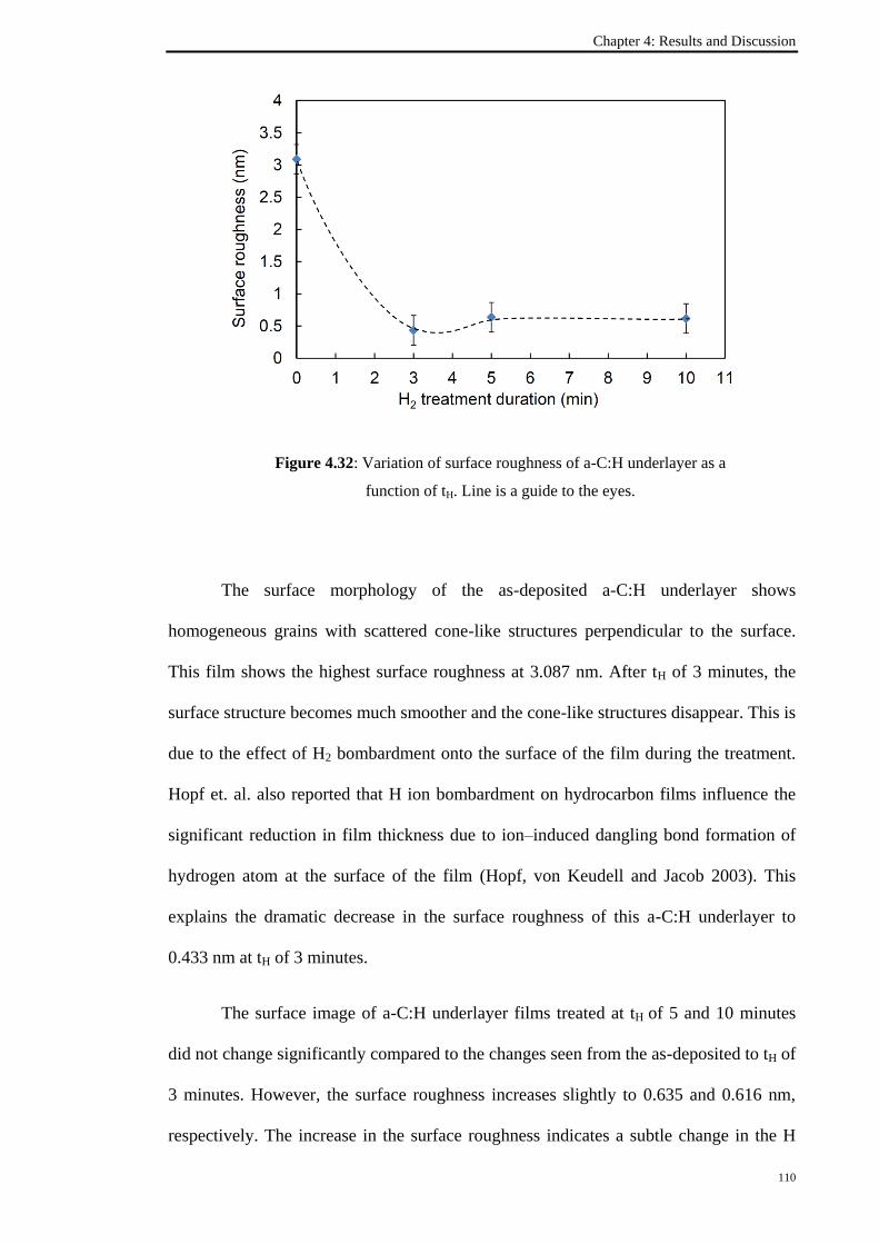
Chapter 4: Results and Discussion
110
Figure 4.32: Variation of surface roughness of a-C:H underlayer as a
function of tH. Line is a guide to the eyes.
The surface morphology of the as-deposited a-C:H underlayer shows
homogeneous grains with scattered cone-like structures perpendicular to the surface.
This film shows the highest surface roughness at 3.087 nm. After tH of 3 minutes, the
surface structure becomes much smoother and the cone-like structures disappear. This is
due to the effect of H2 bombardment onto the surface of the film during the treatment.
Hopf et. al. also reported that H ion bombardment on hydrocarbon films influence the
significant reduction in film thickness due to ion–induced dangling bond formation of
hydrogen atom at the surface of the film (Hopf, von Keudell and Jacob 2003). This
explains the dramatic decrease in the surface roughness of this a-C:H underlayer to
0.433 nm at tH of 3 minutes.
The surface image of a-C:H underlayer films treated at tH of 5 and 10 minutes
did not change significantly compared to the changes seen from the as-deposited to tH of
3 minutes. However, the surface roughness increases slightly to 0.635 and 0.616 nm,
respectively. The increase in the surface roughness indicates a subtle change in the H

Chapter 4: Results and Discussion
111
ion bombardment on the surface. It is believed that the H plasma etching effect is time
dependent, and becomes less dominant since weakly bonded sites would have been
removed by this tH. On the other hand, the atomic hydrogen density increases when the
a-C:H underlayers experienced longer tH. The energy of the impinging H ions is
dependent on the amount of collision that occurs in the plasma. When their energies are
larger than the critical value of atomic displacement in the a-C:H underlayer, the ions
will be able to penetrate the outermost surface of a-C:H underlayer. This process is
called subplantation (Robertson 2002). During this process, the ions will be integrated
into the bulk volume of the subsurface thus contributing to the morphology of a-C:H
underlayer at longer tH. It appears that the subplantation of the H atoms and ions is
dependent on tH and increase with tH after the initial 3 minutes.
4.4.1.2 Chemical bonding properties of a-C:H underlayers
The chemical bonding of the a-C:H underlayers as a function of tH were studied
using FTIR.. These FTIR spectra are shown in Figure 4.33. The spectra can be divided
into two main regions at wavenumber ranges of 1200-1900 cm-1
and 2700-3800 cm-1
.
The absorption bands at 1200-1900 cm-1
are assigned to sp2 phase CC bond; while the
band in the region of 2700-3800 cm-1
are assigned to the bonds of CHn groups and O-H
(Mutsukura and Akita 1999).
These two major regions of the FTIR spectra were deconvoluted and presented
in Figure 4.34. For the region within the range of 1200-1900 cm-1
, the spectra were
fitted for band corresponding to sp2 C, Raman D, sp
3 CH, Raman G, C=C and C=C
stretching at 1350, 1380, 1450, 1580, 1650 and 1700 cm-1
, respectively as shown in
Figure 4.34 (a). Figure 4.34 (b) shows the second region in the range of
2700-3200 cm-1
, whereby the spectra represent sym sp3 CH2, sym sp
3 CH3, asym sp
3
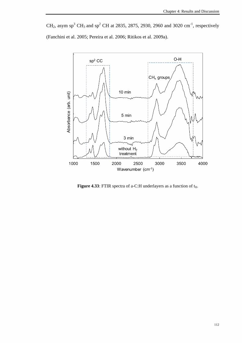
Chapter 4: Results and Discussion
112
CH2, asym sp3 CH3 and sp
2 CH at 2835, 2875, 2930, 2960 and 3020 cm
-1, respectively
(Fanchini et al. 2005; Pereira et al. 2006; Ritikos et al. 2009a).
Figure 4.33: FTIR spectra of a-C:H underlayers as a function of tH.
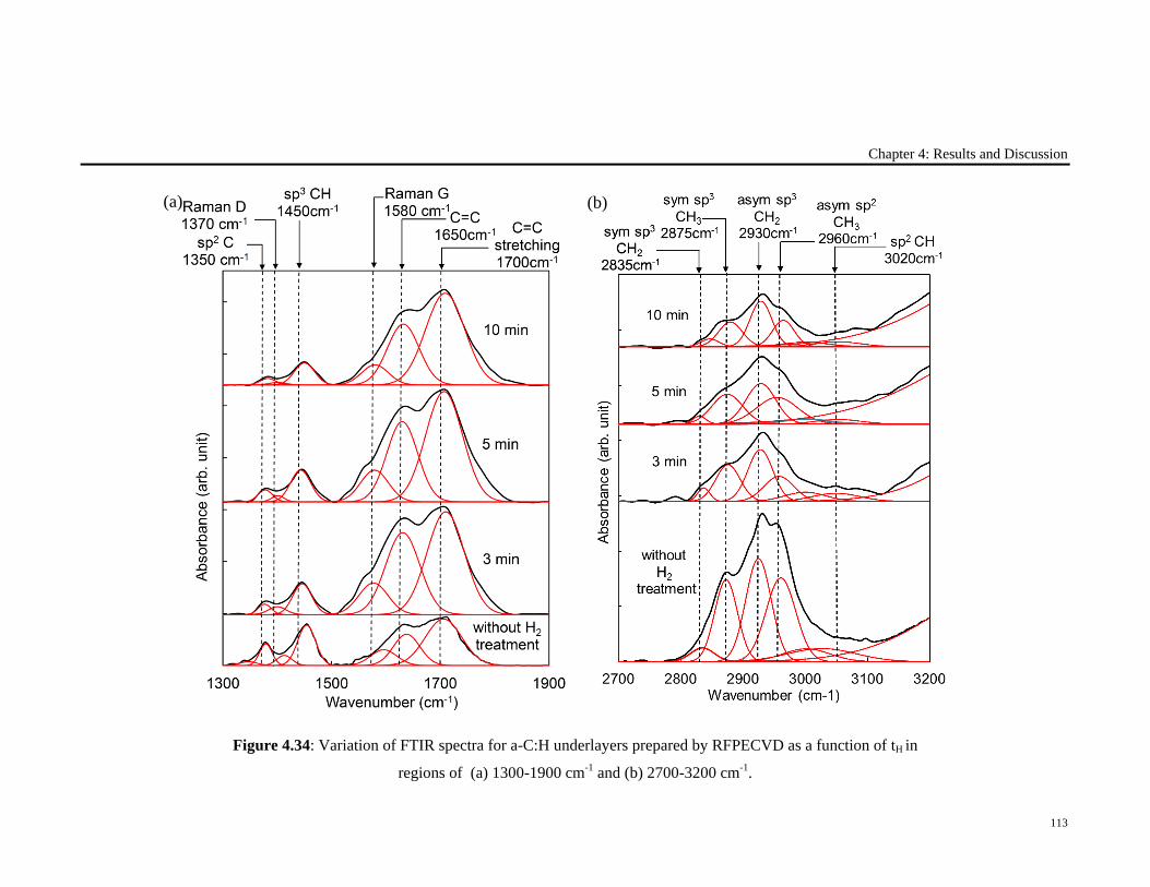
Chapter 4: Results and Discussion
113
Figure 4.34: Variation of FTIR spectra for a-C:H underlayers prepared by RFPECVD as a function of tH in
regions of (a) 1300-1900 cm-1 and (b) 2700-3200 cm-1.
(a) (b)

Chapter 4: Results and Discussion
114
The deconvoluted FTIR spectra depicted in Figure 4.34 show that the functional
groups remains intact even with the H2 treatment on these a-CH underlayer films. In
particular, the sp2 phase region remains almost the same even after tH of 10 minutes. A
similar deduction could be made for the CHn region although it is seen that there are
slight changes in the relative peak intensities of the sp3 CH2 and sp
2 CH3 peaks at 2930
and 2960 cm-1
, respectively. However a more significant change is seen for the overall
spectra as shown in Figure 4.33. While the sp2 CC band does not change, a significant
decrease is seen in the CHn particularly when compared between the as deposited a-C:H
and after tH of 3 minutes.
The decrease in CHn indicates a decrease in H bonds and this is in line with the
proposed H ion bombardment effect on the film surface which creates dangling bonds
(Hopf, von Keudell and Jacob 2003). It appears that the ion bombardment would
preferentially reduce this CHn bonds. With the increase in tH, the CHn bond intensities
remains almost the same which support the saturation in the etching effect of the H
bombardment that leads instead to the subplantation of these ions or atom.
4.4.1.3 Raman analysis
The Raman spectra of these a-C:H underlayers were obtained in the Raman shift
range of 1000–2000 cm-1
using UV excitation of 325 nm. The raw Raman spectra
depicted in Figure 4.35 (a) shows two prominent peaks at around 1380 and 1600 cm-1
assigned to their D and G band, respectively. The Raman spectrum of the as-deposited
a-C:H underlayer has strong PL background resulting in a positive slope of the
spectrum. This was also observed by Marchon et. al in hydrogenated carbon films
prepared by DC-magnetron sputtering technique (Marchon et al. 1997). The PL
background is due to hydrogen saturation of non-radiative recombination centers in the

Chapter 4: Results and Discussion
115
film (Escobar-Alarcón et al. 2005) which promotes the PL emission in this material.
The increase in H bond in a-C:H usually leads to an increase in PL emission. In contrast
having undergone H treatment even as early as tH of 3 minutes the PL background
reduces significantly which completely eliminates the slope. This indicates a reduction
in H bond in the film in line with the deduction in FTIR and AFM analysis.
The corrected and fitted Raman spectra for a-C:H underlayers as a function of tH
are shown in Figure 4.35 (b), while the corresponding fitting parameters including the
variations in G and D peak positions, FWHM and ID/ IG ratio are shown in Figure 4.36.
In general, the G peak position lies at a constant wavenumber approximately 1597 cm-1
regardless of tH. This value being higher than that of graphite (1550 cm-1
) though not
exceeding the limit of graphitic carbon implies that these films have high degree of
graphitization but also exhibit characteristic of olefinic (chain sp2 group) with shorter
bond length (Gilkes et al. 1998). However it is the D band which best explains the
changes in the film with tH. The D peak red-shifted drastically with tH particularly from
the as-deposited to the initial tH of 3 minutes. The red-shift in D peak could be attributed
to either a decrease in the number of ordered aromatic ring or a strained or curved
graphitic plane (Ferrari and Robertson 2000; Yu et al. 2002). In contrast, the FWHMD
increases drastically with tH particularly from the as-deposited to the initial tH of
3 minutes. This implies a broadening in the width of the D peak which is correlated to
the increase in disorder due to a distribution of clusters with diferent orders and
dimensions. The changes in the initial tH of 3 minutes coincides with the proposed
etching and reduction of H bonds on the film surface with H ion bombardment. Thus it
can be deduced that in the initial tH of 3 minutes, there appears to be an increase in
disorder due to the breaking of the CH bonds, which in turns causes a change in the
number of aromatic rings and a redistribution of the clusters containing these rings. It
can also be stipulated that the redistribution of the clusters also causes the changes in
Chapter 4: Results and Discussion
116
the surface morphology of the films seen in the AFM imaging whereby the surface was
smoothen out and the roughness decreases significantly. It is deemed true that the
clusters in the film consisting of sp2 domains may be taken as ordered domains by
Raman, these clusters are the cone-like structures on the surface which induce the high
roughness in AFM analysis.
With the increase in tH above 3 minutes, the D peak blue-shifted slightly, while
the FWHMD decreases, implying an slight increase in ordering and an increase in the
number or size of the ordered sp2 aromatic ring clusters. Indeed this is in-line with the
slight increase in the surface roughness (Figure 4.32) which further supports the
deduction proposed concerning the effect of the H ion treatment.

Chapter 4: Results and Discussion
117
Figure 4.35: The raw Raman spectra with strong background (a) and the Raman spectra after the background extraction (b) for a-C:H
underlayers as a function of tH.
(a) (b)

Chapter 4: Results and Discussion
118
Figure 4.36: Raman analysis of a-C:H underlayers prepared
as a function hydrogen treatment duration. Line is guide to the eyes.
(a) (b)
(c) (d)
(e)

Chapter 4: Results and Discussion
119
4.4.2 Effect on Resulting CNx/a-C:H Formation
4.4.2.1 Surface and cross-sectional images
The next step is to investigate the formation of ns-CNx deposited onto these
a-C:H underlayers treated at different tH. The surface and cross-sectional FESEM
images of these ns-CNx/a-C:H are presented in Figure 4.37 as a function of tH. The
ns-CNx prepared on as-deposited a-C:H underlayer formed petal–like structure which
conglomerate to form solid-like bulk structures. The ns-CNx grown on a-C:H underlayer
treated at 3 minutes shows similar structures as those deposited on the as-deposited
a-C:H underlayer. However these are formed as distinct vertical fiber-like structures
which are well separated as compared to the conglomeration of those mention for its
predecessor. Conversely, the structures of the ns-CNx evolved with the increase of tH
above 3 minutes. It is seen that the ns-CNx/a-C:H formed at tH of 5 minutes were
produced as well defined short nanotips. The length and distribution of these CNx
nanotips are quite uniform with the average length and diameter calculated from the
cross-sectional image to be approximately 125 ± 1 nm and 78.0 ± 0.2 nm, respectively.
With the increase in tH to 10 minutes, the ns-CNx/a-C:H forms similar structure as those
at tH of 5 minutes but the length, diameter and distribution appears to change. The
length and diameter of these nanotips appear to increase though the growth appears not
to be so uniform with large disparities where the length varies between 20 to 211 nm
and the diameter between 39 to 60 nm. It is also noted that the ns-CNx produced on the
as-deposited a-C:H and at tH of 3 minutes appears to grow as part of the underlayer film.
No clear distinction could be made to identify the boundary between the root of the
ns-CNx and the top layer of the a-C:H underlayer. In contrast, the boundary between the
CNx nanotips formed at tH of 5 and 10 minutes is easily distinguish.
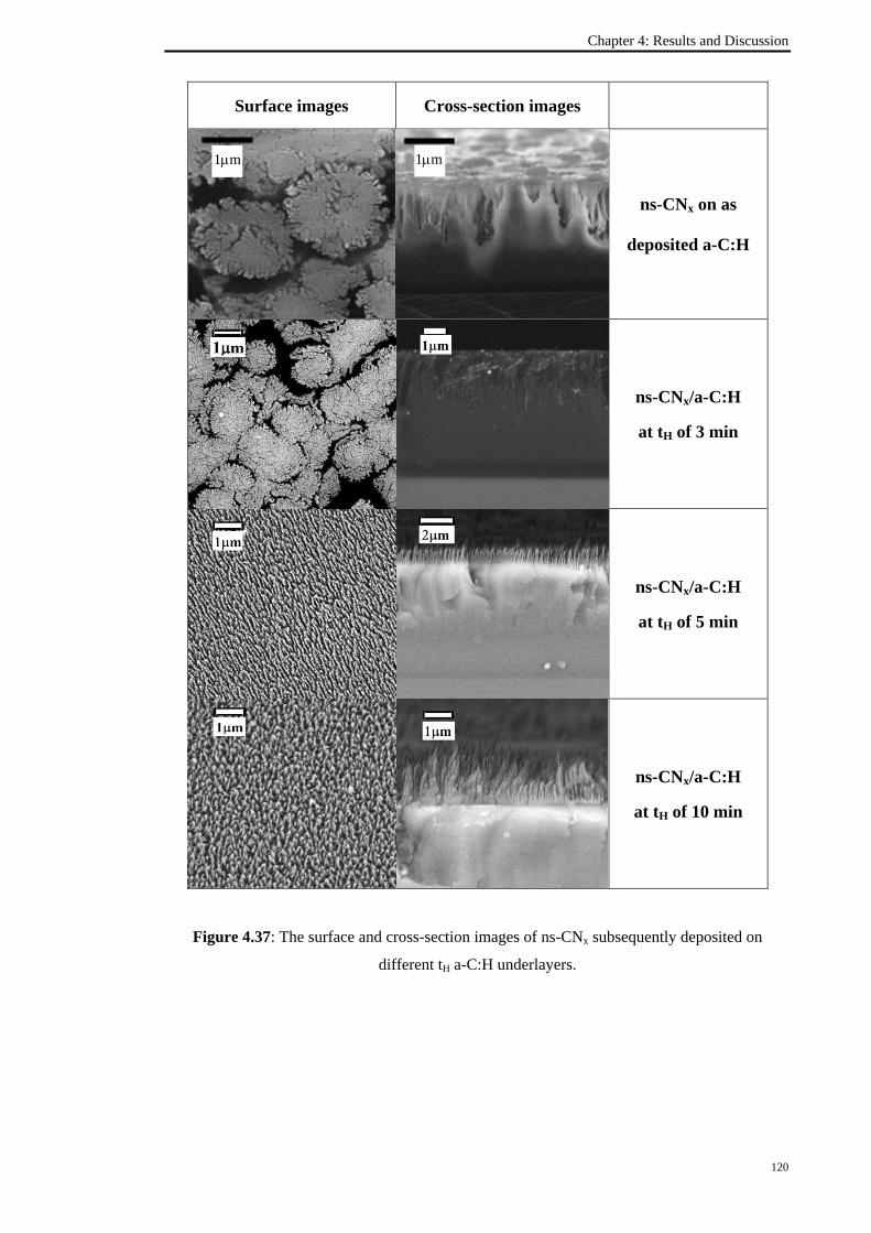
Chapter 4: Results and Discussion
120
Surface images Cross-section images
ns-CNx on as
deposited a-C:H
ns-CNx/a-C:H
at tH of 3 min
ns-CNx/a-C:H
at tH of 5 min
ns-CNx/a-C:H
at tH of 10 min
Figure 4.37: The surface and cross-section images of ns-CNx subsequently deposited on
different tH a-C:H underlayers.
1m 1m
Chapter 4: Results and Discussion
121
4.4.2.2 Auger electron spectroscopy measurement of ns-CNx
The chemical composition of the ns-CNx was determined as the relative
concentration of N and C (N/C) calculated from AES measurement. Figure 4.38 shows
the variation of N/C ratio of these ns-CNx as a function of different tH for the treatment
of a-C:H underlayers. The ns-CNx grown on the as-deposited a-C:H underlayer has the
highest N/C ratio at 0.2 . With the H2 treatment of the a-C:H underlayer and increase in
tH the N/C ratio of the ns-CNx formed reduces gradually after the initial tH of 3 minutes.
This indicates a significant decrease in N incorporation in the ns-CNx with the H
treatment of the a-C:H underlayer. From the previous sections on the study of rf power
and deposition duration, it was seen that CNx nanorods were produced at the high a-C:H
surface roughness and highest N/C ratio of the ns-CNx, which was correlated to
presence and ordering of the sp2 clusters. In contrast, with the H2 treatment on the
a-C:H underlayers, CNx nanotips are formed at low surface roughness while having low
N/C ratio. Indeed, other researcher has reported the formation of CNx nanotips formed
on a-C:H films at high deposition temperature, having also low N content (Wang et al.
2005). According to these researchers, the N2 in the plasma not only acts as reactants
but also as etching agents. These N etching ions help to form the nanostructure but do
not get incorporated into the film, thus keep the N incorporation low. However in this
work there is an obvious dependence of the change in ns-CNx and the surface condition
of the a-C:H films brought about by the H2 plasma treatment. The earlier studies on the
Raman scattering of these a-C:H underlayer as a function of tH implies a redistribution
and decrease in the size and/or number of sp2
clusters. These clusters may act as the
nucleation sites for the growth of the ns-CNx (Wang et al. 2011) and with the changes in
these sp2 clusters, the sites may become smaller and thus decreases the size of the
ns-CNx and forms the nanotips. The redistribution of the cluster by the H2 plasma also
results on the uniform distribution of the nanotips.

Chapter 4: Results and Discussion
122
Figure 4.38: Variation of nitrogen to carbon, N/C ratio of ns-CNx
deposited on different tH a-C:H underlayers.
4.4.2.3 FTIR spectra of ns-CNx
FTIR analysis was carried out on the ns-CNx grown on a-C:H underlayers as a
function of tH. The variation their spectra are shown in Figure 4.39 in the region of
1000–4000 cm-1
, while the three separated main regions within the range of 1100–1900,
2000–2300 and 2700–3800 cm
-1 are shown in Figure 4.40. Similar to the previous
sections the first region within the range of 1100–1900 cm-1
is attributed to sp2-C bonds
including C-C, C-N, C=C and C=N. The second region in the range of 2000–2300 cm-1
is assigned to the sp1-C bonds including nitrile and isonitrile bonds. Lastly, the third
region in the range of 2700–3800 cm-1
represents sp3-C bonds, O-H and N-H groups
(Motta and Pereyra 2004; Pereira et al. 2006; Ritikos et al. 2009b).
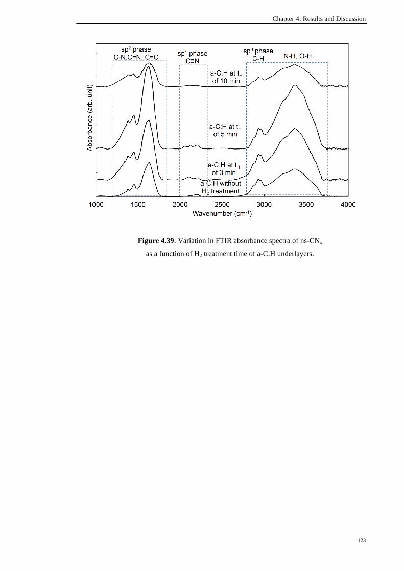
Chapter 4: Results and Discussion
123
Figure 4.39: Variation in FTIR absorbance spectra of ns-CNx
as a function of H2 treatment time of a-C:H underlayers.

Chapter 4: Results and Discussion
124
Figure 4.40: The FTIR spectra for ns-CNx deposited on different tH of a-C:H underlayers
in the range of (a) sp2, (b) sp1 and (c) sp3 phases.
(a) (b) (c)

Chapter 4: Results and Discussion
125
The sp2 and sp
3-C bonds within the ranges of 1100–1900 and 2700–3800 cm
-1,
respectively, remains almost the same regardless of tH. The remarkable difference was
seen in the spectra range of 1900-2300 cm-1
as shown in the overlaid spectra shown in
Figure 4.41 for this region. As mentioned before, this absorption band is related to
nitrile and/or isonitrile (C≡N) bonds in the chemical structure of the material. The
region consists of five overlapping bands associated to HCN at 2050 cm-1
, aromatic
ring, C2H5 and CH3 bonded to isonitrile (-N≡C) located at 2105, 2160 and 2190 cm-1
,
respectively, together with the aromatic ring and hydrocarbon (CH3, C2H5, etc.) bonded
to nitrile (-C≡N) at 2215 and 2245 cm-1
, respectively (Mutsukura and Akita 1999). The
deconvoluted peaks using standard Gaussian curve-fitting method are shown in Figure
4.42.
Figure 4.41: The FTIR spectra in the wavenumber range of 1900-2300 cm-1 of
ns-CNx as a function of tH a-C:H underlayers.
Chapter 4: Results and Discussion
126
The deconvoluted spectra show a certain progression in the formation and
preferential sp1-C bonds which makes up the ns-CNx film. While isonitrile (-N≡C)
bonds appear to be the preferential type compared to nitrile (-C≡N) for all these
samples, the functional group which are attached to these bonds appears to be
important. The ns-CNx deposited onto the as-deposited a-C:H underlayer shows the
preference of isonitrile bonded to aliphatic CH3 (CH3─N≡C), with the absorption peaks
corresponding to isonitrile bonded to aliphatic C2H5 and nitrile bonded to aromatic rings
being slightly less stronger.
In contrast, when these ns-CNx were deposited onto the treated a-C:H
underlayers, a significant shift in the preferential bonds to isonitrile bonded to aromatic
rings is seen. Its absorption peaks strengthen considerably relative to the other bonding
and indicates the increase in aromatic rings and thus the sp2 clusters in the
nanostructures. This signifies the importance of the aromatic rings in the formation of
these vertically aligned nanostructures. This may also have led to the separation of the
nanostructure strands which allows the nanofibers and nanotips to form apart rather than
conglomerate like the ns-CNx formed on the as-deposited a-C:H.
The variation in the spectra also shows a significant increase in the formation of
HCN particularly for the ns-CNx/a-C:H treated at tH of 5 and 10 minutes. These
elements could also be found in gaseous form and are normaaly volatile. Thus, it is
probable that during the deposition, these elements may be a substantial part of the
species in the plasma. Due to the volatile nature of this element, a large part of it may
have been discarded as residual rather than being incorporated into the film. Thus this
reduces the N incorporation in the film resulting in the low N/C ratio in the
ns-CNx/a-C:H with tH.

Chapter 4: Results and Discussion
127
Figure 4.42 : Gaussian fitting profiles for FTIR spectra in wavenumber region of
1900-2400 cm-1 for a-C:H underlayer at tH of 3, 5, 10 minutes and
a-C:H underlayer without H2 treatment.
4.4.3 Summary
The effects of H2 treatment at various tH on the structure and morphology of
a-C:H underlayer were studied. H2 treatment alters the surface morphologies of these
films giving a smoother surface roughness with the increase in tH. This was related to an
increase in the disorder in the film due to the decrease in size and/or number of the sp2
clusters and a redistribution of these clusters. This in turn was speculated to be due to
the H etching and subplantation during H ion bombardment on the film surface. It was
shown that by using this treatment method, the ns-CNx deposited onto this underlayer
1m

Chapter 4: Results and Discussion
128
film could be manipulated. CNx nanotips were successfully produced by RFPECVD at
low temperature on a-C:H underlayers treated at tH above 3 minutes. While all these
ns-CNx/a-C:H films still shows the preferential formation of isonitrile bonds, the
formation of distinct and separated strands were induce by the increase in aromatic
rings in the film being bonded to these isonitrile. The decrease in the N incorporation
with the formation of the nanotip may be due to production of volatile HCN in the
plasma which did not contribute to the growth of the film.

Chapter 5: Conclusion and Future Works
129
CHAPTER 5 : CONCLUSION AND FUTURE WORKS
5.1 Conclusion
The deposition of various types of ns-CNx through the modification of the
structural properties of pre-deposited a-C:H underlayer has been studied. Both ns-CNx
and a-C:H underlayer films were successfully grown using RFPECVD technique
without catalyst assistance at 100 oC. The ns-CNx were fabricated at fixed deposition
parameters including RF power, deposition duration, temperature, pressure and gases
flow rate ratio while the deposition parameters of the a-C:H underlayer were varied
using different preparation condition or post-deposition treatments. In the first two sets,
ns-CNx samples were deposited on a-C:H underlayers prepared using different
deposition time duration (tD) and RF power (PUL) while in the third set, the ns-CNx were
deposited on a-C:H underlayers treated with H2 plasma at different time duration (tH).
Under these conditions different types of ns-CNx was formed including rigid and
vertically aligned nanorods, fiber-like, flower-like nanostructures and nanotips.
The structural properties of the a-C:H underlayer influences the formation of
ns-CNx. In the study of deposition time duration of 5, 10, 15 and 30 minutes, it was
found that high surface roughness of a-C:H underlayer induce the formation of rigid and
vertically aligned CNx nanorods. The a-C:H underlayer deposited for 10 minutes shows
the highest surface roughness inducing the protrusion of broad-tipped cone-like features
from the film surface. This was shown to be associated with the presence and ordering
of sp2 clusters in the a-C:H film.
The contribution of the surface roughness was further studied by varying the
applied RF power. This effectively influences the ion bombardment effect on the
Chapter 5: Conclusion and Future Works
130
growing film surface and significantly changes the structural properties of the a-C:H
underlayer. From the FTIR results, it was obtained that the film with highest surface
roughness shows low CHn band indicating low H content in the film attributed by the
dominant sp2 C bonds. This confirms the deduction made in the earlier study where the
highest surface roughness of the a-C:H underlayer was due to the presence and ordering
of sp2 clusters in the a-C:H film. In this work, it was also established that by tuning the
RF power, a unique flower-like CNx nanostructures can be grown.
The study on the variation of H2 plasma treatment time duration of 3, 5 and 10
minutes shows that H bombardment effects influenced the structural properties of the a-
C:H underlayers. These results showed that the formation of dangling bonds as a results
of bombardment of the surface with hydrogen atoms form a smooth surface of a-C:H
underlayers as a consequent of the disorder in the film structure due to the decrease in
size and/or number of sp2 clusters and the redistribution on these clusters. The smooth
a-C:H underlayers that were treated for a duration of 5 and 10 minutes led to the
formation of CNx nanotips.
Different structures of ns-CNx were formed as a result of different a-C:H
underlayer properties. The nanostructures formed included rigid vertically aligned
nanorods and nanotips. Rigid, vertically aligned CNx nanorods exhibit the highest N
incorporation with N/C ratio of 0.2. This indicates that high N incorporation is crucial in
the formation of this type of structure. CNx nanotips show relatively lower N
incorporation whereby N in the plasma act as etching agents in the growth process and
do not get easily incorporated into the film structure. In general, the chemical bonding
of these different ns-CNx structures show preference of N bonding in the form of nitrile
(-C≡N) and isonitrile (-N≡C). From this chemical bonding analysis, the preference of
aromatic ring bonded to isonitrile bonds favours the formation of rigid, vertically
aligned nanorods of CNx. Throughout this work, it is proposed that a-C:H underlayer

Chapter 5: Conclusion and Future Works
131
acts as template or seed layer that helps the formation of nucleation site for ns-CNx
growth.
5.2 Future Works
Due to the introductory nature of this work and constraint in time and resources
a number of different aspects in this study were not able to be carried out. Some of these
aspects are listed here as suggestion for future works:
(1) Material characterization particularly on the properties of these ns-CNx,
measurements such as high resolution transmission electron microscopy
(HRTEM) and x-ray photo spectroscopy are needed to further identify the
nature and crystallinity of these structures.
(2) Growth progress and mechanism for both the a-C:H underlayer and ns-CNx
that could be done by studying the growth as a function of deposition duration
for both layers.
(3) Exploring different areas of application for the films.
(i) CNx nanotips as scanning probe-tip and electron emitting devices seem
high in view of its size and distribution of the growth.
(ii) CNx nanorods as potential material for humidity or gas sensors and
hydrogen storage material.

References
132
REFERENCES
Apostol, I., Stefan, N., Luculescu, C. R., Birjega, R., Socol, M., Miroiu, M., &
Mihailescu, I. N. (2011). Pulsed laser deposition of semiconducting crystalline
double-doped barium titanate thin films on nickel substrates. Applied Surface
Science, 257(8), 3570-3576.
Ayala, P., Arenal, R., Rümmeli, M., Rubio, A., & Pichler, T. (2010). The doping of
carbon nanotubes with nitrogen and their potential applications. Carbon, 48(3),
575-586.
Ayala, P., Grüneis, A., Gemming, T., Büchner, B., Rümmeli, M., Grimm, D., Filho, H.
D. F. (2007a). Influence of the catalyst hydrogen pretreatment on the growth of
vertically aligned nitrogen-doped carbon nanotubes. Chemistry of Materials,
19(25), 6131-6137.
Ayala, P., Grüneis, A., Kramberger, C., Rümmeli, M., Solorzano, I., Freire Jr, F., &
Pichler, T. (2007b). Effects of the reaction atmosphere composition on the
synthesis of single and multiwalled nitrogen-doped nanotubes. The Journal of
Chemical Physics, 127, 184709.
Baehr, O., Thevenin, P., Bath, A., Koukab, A., Losson, E., & Lepley, B. (1997).
Preparation of boron nitride thin films by microwave plasma enhanced CVD, for
semiconductor applications. Materials Science and Engineering: B, 46(1), 101-
104.
Bai, X., Cao, C., & Xu, X. (2010). Formation and characterization of flower-like carbon
nitride by pyrolysis of melamine. Materials Science and Engineering: B, 175(2),
95-99.
Bai, X., Zhong, D., Zhang, G., Ma, X., Liu, S., Wang, E., Shaw, D. T. (2001).
Hydrogen storage in carbon nitride nanobells. Applied Physics Letters, 79(10),
1552-1554.
Banerjee, I., Kumari, N., Singh, A. K., Kumar, M., Laha, P., Panda, A., Mahapatra, S.
(2010). Influence of RF power on the electrical and mechanical properties of
nano-structured carbon nitride thin films deposited by RF magnetron sputtering.
Thin Solid Films, 518(24), 7240-7244.
Brown, B., Parker, C. B., Stoner, B. R., & Glass, J. T. (2011). Growth of vertically
aligned bamboo-like carbon nanotubes from ammonia/methane precursors using
a platinum catalyst. Carbon, 49(1), 266-274.
Cao, P., Zhu, D., Liu, W., & Ma, X. (2007). The effect of substrate morphology on the
diameter distribution of carbon nanotubes grown on silica and ceramic
substrates. Materials Letters, 61(8), 1899-1903.
Casiraghi, C., Piazza, F., Ferrari, A. C., Grambole, D., & Robertson, J. (2005). Bonding
in hydrogenated diamond-like carbon by Raman spectroscopy. Diamond and
Related Materials, 14(3-7), 1098-1102.
Cespedes, J., Corbella, C., Bertran, E., Viera, G., & Galan, M. (2005). Characteristics of
Carbon and Carbon‐Nitride Nanostructures Produced by Plasma Deposition
from Ammonia and Methane or Acetylene. Fullerenes, Nanotubes, and Carbon
Nanostructures, 13(S1), 447-455.
Chan, L., Hong, K., Xiao, D., Hsieh, W., Lai, S., Shih, H., Cheng, H. (2003). Role of
extrinsic atoms on the morphology and field emission properties of carbon
nanotubes. Applied Physics Letters, 82, 4334.
Chan, L. H., Hong, K. H., Xiao, D. Q., Lin, T. C., Lai, S. H., Hsieh, W. J., & Shih, H.
C. (2004). Resolution of the binding configuration in nitrogen-doped carbon
nanotubes. Physical Review B, 70(12), 125408.
References
133
Che, R., Peng, L. M., & Wang, M. (2004). Electron side-emission from corrugated CN
nanotubes. Applied Physics Letters, 85, 4753.
Choi, H. C., Bae, S. Y., Jang, W. S., Park, J., Song, H. J., Shin, H. J., Ahn, J. P. (2005).
Release of N2 from the carbon nanotubes via high-temperature annealing. The
Journal of Physical Chemistry B, 109(5), 1683-1688.
Choi, W. S., Heo, J., Chung, I., & Hong, B. (2005). The effect of RF power on
tribological properties of the diamond-like carbon films. Thin Solid Films,
475(1-2), 287-290.
Chu, P. K., & Li, L. (2006). Characterization of amorphous and nanocrystalline carbon
films. Materials Chemistry and Physics, 96(2-3), 253-277.
Cui, S., Scharff, P., Siegmund, C., Schneider, D., Risch, K., Klötzer, S., Schawohl, J.
(2004). Investigation on preparation of multiwalled carbon nanotubes by DC arc
discharge under N2 atmosphere. Carbon, 42(5–6), 931-939.
Cuomo, J., Leary, P., Yu, D., Reuter, W., & Frisch, M. (1979). Reactive sputtering of
carbon and carbide targets in nitrogen. Journal of Vacuum Science and
Technology, 16(2), 299-302.
Dang, C., & Wang, B. (2012). Study on structures and photoluminescence of
nitrogenated carbon nanotip arrays synthesized by plasma assisted hot filament
chemical vapor deposition. Applied Surface Science 258(17), 6692-6698.
Droppa Jr, R., Hammer, P., Carvalho, A. C. M., dos Santos, M. C., & Alvarez, F.
(2002). Incorporation of nitrogen in carbon nanotubes. Journal of Non-
Crystalline Solids, 299–302, Part 2(0), 874-879.
Escobar-Alarcón, L., Arrieta, A., Camps, E., Romero, S., & Camacho-Lopez, M.
(2005). Infrared and Raman characterization of amorphous carbon nitride thin
films prepared by laser ablation.Superficies y Vacio, 9-12.
Fanchini, G., Mandracci, P., Tagliaferro, A., Rodil, S. E., Vomiero, A., & Della Mea, G.
(2005). Growth and characterisation of polymeric amorphous carbon and carbon
nitride films from propane. Diamond and Related Materials, 14(3–7), 928-933.
Ferrari, A., & Robertson, J. (2000). Interpretation of Raman spectra of disordered and
amorphous carbon. Physical Review B, 61(20), 14095.
Ferrari, A., Rodil, S., & Robertson, J. (2003). Interpretation of infrared and Raman
spectra of amorphous carbon nitrides. Physical Review B, 67(15), 155306.
Ferrari, A. C. (2007). Raman spectroscopy of graphene and graphite: Disorder,
electron–phonon coupling, doping and nonadiabatic effects. Solid State
Communications, 143(1), 47-57.
Ganesan, Y., Peng, C., Lu, Y., Ci, L., Srivastava, A., Ajayan, P. M., & Lou, J. (2010).
Effect of nitrogen doping on the mechanical properties of carbon nanotubes.
ACS Nano 4(12), 7637-7643.
Gielen, J., Kessels, W., Van de Sanden, M., & Schram, D. (1997). Effect of substrate
conditions on the plasma beam deposition of amorphous hydrogenated carbon.
Journal of Applied Physics, 82, 2643.
Gilkes, K. W. R., Sands, H. S., Batchelder, D. N., Milne, W. I., & Robertson, J. (1998).
Direct observation of sp3 bonding in tetrahedral amorphous carbon UV Raman
spectroscopy. Journal of Non-Crystalline Solids, 227–230, Part 1(0), 612-616.
Glerup, M., Steinmetz, J., Samaille, D., Stéphan, O., Enouz, S., Loiseau, A., Bernier, P.
(2004). Synthesis of N-doped SWNT using the arc-discharge procedure.
Chemical Physics Letters, 387(1–3), 193-197.
Gong, K., Du, F., Xia, Z., Durstock, M., & Dai, L. (2009). Nitrogen-doped carbon
nanotube arrays with high electrocatalytic activity for oxygen reduction.
Science, 323(5915), 760.
References
134
He, M., Zhou, S., Zhang, J., Liu, Z., & Robinson, C. (2005). CVD growth of N-doped
carbon nanotubes on silicon substrates and its mechanism. The Journal of
Physical Chemistry B, 109(19), 9275-9279.
Honda, S., Lee, K. Y., Fujimoto, K., Tsuji, K., Ohkura, S., Katayama, M., Oura, K.
(2002). Formation of carbon nanofiber films by RF magnetron sputtering
method. Physica B: Condensed Matter, 323(1–4), 347-349.
Hopf, C., von Keudell, A., & Jacob, W. (2003). The influence of hydrogen ion
bombardment on plasma-assisted hydrocarbon film growth. Diamond and
Related Materials, 12(2), 85-89.
Hu, J., Yang, P., & Lieber, C. M. (1998). Nitrogen driven structural transformation in
carbon nitride materials. Applied Surface Science, 127, 569-573.
Huang, C. J., Chih, Y. K., Hwang, J., Lee, A. P., & Kou, C. S. (2003). Field emission
from amorphous-carbon nanotips on copper. Journal of Applied Physics, 94(10),
6796-6799.
Hung, J.-M., Lin, L.-H., Shih, Y.-H., Liu, C.-M., Cheng, H.-C., & Ou, K.-L. (2011).
Research of microstructural characteristics on nanocrystalline diamond by
microwave plasma CVD. Applied Surface Science, 257(13), 5508-5512.
Iijima, S. (1991). Helical microtubules of graphitic carbon. Nature, 354(6348), 56-58.
Inaba, H., Fujimaki, S., Furusawa, K., & Todoroki, S. (2002). ECR-plasma parameters
and properties of thin DLC films. Vacuum, 66(3–4), 487-493.
Iseki, T. (2009). Target utilization of planar magnetron sputtering using a rotating tilted
unbalanced yoke magnet. Vacuum, 84(2), 339-347.
Ito, H., Nozaki, T., Saikubo, A., Yamada, N., Kanda, K., Niibe, M., & Saitoh, H.
(2008). Hydrogen-storage characteristics of hydrogenated amorphous carbon
nitrides. Thin Solid Films, 516(19), 6575-6579.
Jawhari, T., Roid, A., & Casado, J. (1995). Raman spectroscopic characterization of
some commercially available carbon black materials. Carbon, 33(11), 1561-
1565.
Jayatissa, A. H., Sato, F., Saito, N., Ohnishi, H., Takizawa, K., Nakanishi, Y., &
Yamaguchi, T. (1998). Structural properties of carbon films deposited by pulsed
ArF laser ablation: effects of substrate temperature, bias and H< sub> 2</sub>
pressure. Materials Science and Engineering: B, 55(1), 143-152.
Jun, C., Ning-sheng, X., En-ge, W., Shao-zhi, D., Di-hu, C., & Ai-xiang, W. (1998). A
Study of Field Electron Emission from Thin Amorphous-Carbon-Nitride Films.
Chinese Physics Letters, 15, 539.
Kim, B. K., & Grotjohn, T. A. (2000). Comparison of a-C:H films deposited from
methane–argon and acetylene–argon mixtures by electron cyclotron resonance–
chemical vapor deposition discharges. Diamond and Related Materials, 9(1),
37-47.
Kim, J.-P., Noh, Y.-R., Kim, J.-U., & Park, J.-S. (2011). Electron-emission properties of
carbon nanotube micro-tips coated by amorphous carbon nitride films. Thin
Solid Films, 519(22), 7899-7903.
Koh, G., Zhang, Y.-W., & Pan, H. (2012). First-principles study on hydrogen storage by
graphitic carbon nitride nanotubes. International Journal of Hydrogen Energy,
37(5), 4170-4178.
Koós, A. A., Dowling, M., Jurkschat, K., Crossley, A., & Grobert, N. (2009). Effect of
the experimental parameters on the structure of nitrogen-doped carbon
nanotubes produced by aerosol chemical vapour deposition. Carbon, 47(1), 30-
37.
Krstić, V., Rikken, G., Bernier, P., Roth, S., & Glerup, M. (2007). Nitrogen doping of
metallic single-walled carbon nanotubes: n-type conduction and dipole
scattering. EPL (Europhysics Letters), 77, 37001.

References
135
Kurt, R., Bonard, J. M., & Karimi, A. (2001a). Morphology and field emission
properties of nano-structured nitrogenated carbon films produced by plasma
enhanced hot filament CVD. Carbon, 39(11), 1723-1730.
Kurt, R., Bonard, J. M., & Karimi, A. (2001b). Structure and field emission properties
of decorated C/N nanotubes tuned by diameter variations. Thin Solid Films,
398–399(0), 193-198.
Lai, S. H., Chen, Y. L., Chan, L. H., Pan, Y. M., Liu, X. W., & Shih, H. C. (2003). The
crystalline properties of carbon nitride nanotubes synthesized by electron
cyclotron resonance plasma. Thin Solid Films, 444(1-2), 38-43.
Lazar, G., Zellama, K., Vascan, I., Stamate, M., Lazar, I., & Rusu, I. (2005). Infrared
absorption properties of amorphous carbon films. Journal of Optoelectronics
and Advanced Materials, 7(2), 647-652.
Lee, S. P., Lee, J. G., & Chowdhury, S. (2008). CMOS humidity sensor system using
carbon nitride film as sensing materials. Sensors, 8(4), 2662-2672.
Li, J., Cao, C., Hao, J., Qiu, H., Xu, Y., & Zhu, H. (2006). Self-assembled one-
dimensional carbon nitride architectures. Diamond and Related Materials,
15(10), 1593-1600.
Lin, C. H., Chang, H. L., Hsu, C. M., Lo, A. Y., & Kuo, C. T. (2003). The role of
nitrogen in carbon nanotube formation. Diamond and Related Materials, 12(10–
11), 1851-1857.
Liu, A. Y., & Cohen, M. L. (1989). Prediction of new low compressibility solids.
Science, 245(4920), 841-842.
Liu, H., Zhang, Y., Li, R., Sun, X., Désilets, S., Abou-Rachid, H., Lussier, L.-S. (2010).
Structural and morphological control of aligned nitrogen-doped carbon
nanotubes. Carbon, 48(5), 1498-1507.
Liu, J., Webster, S., & Carroll, D. L. (2005). Temperature and flow rate of NH3 effects
on nitrogen content and doping environments of carbon nanotubes grown by
injection CVD method. The Journal of Physical Chemistry B, 109(33), 15769-
15774.
Liu, X. W., Chan, L., Hong, K., & Shih, H. (2002a). Effect of bias voltage on the
formation of aC: N nanostructures in ECR plasmas. Thin Solid Films, 420, 212-
218.
Liu, X. W., Lin, C. H., Chao, L. T., & Shih, H. C. (2000). Electron field emission from
amorphous carbon nitride nanotips. Materials Letters, 44(5), 304-308.
Liu, X. W., Lin, J. H., Hsieh, W. J., & Shih, H. C. (2002b). Morphology and
characterization of highly nitrogenated, aligned, amorphous carbon nano-rods
formed on an alumina template by ECR-CVD. Diamond and Related Materials,
11(3-6), 1193-1199.
Lowther, J. (1998). Defective and amorphous structure of carbon nitride. Physical
Review B, 57(10), 5724.
Maldonado, S., Morin, S., & Stevenson, K. J. (2006). Structure, composition, and
chemical reactivity of carbon nanotubes by selective nitrogen doping. Carbon,
44(8), 1429-1437.
Maldonado, S., & Stevenson, K. J. (2005). Influence of nitrogen doping on oxygen
reduction electrocatalysis at carbon nanofiber electrodes. The Journal of
Physical Chemistry B, 109(10), 4707-4716.
Marcelli, A., Cricenti, A., Kwiatek, W. M., & Petibois, C. (2012). Biological
applications of synchrotron radiation infrared spectromicroscopy. Biotechnology
Advances doi:/10.1016/j.biotechadv.2012.02.012.
Marchon, B., Gui, J., Grannen, K., Rauch, G. C., Ager III, J. W., Silva, S., & Robertson,
J. (1997). Photoluminescence and Raman spectroscopy in hydrogenated carbon
films. Magnetics, IEEE Transactions on, 33(5), 3148-3150.
References
136
Meng, X., Zhong, Y., Sun, Y., Banis, M. N., Li, R., & Sun, X. (2011). Nitrogen-doped
carbon nanotubes coated by atomic layer deposited SnO2 with controlled
morphology and phase. Carbon, 49(4), 1133-1144.
Meyyappan, M., Delzeit, L., Cassell, A., & Hash, D. (2003). Carbon nanotube growth
by PECVD: a review. Plasma Sources Science and Technology, 12, 205.
Miyajima, Y., Henley, S. J., & Silva, S. R. P. (2011). Hydrogenated amorphous carbon
and carbon nitride films deposited at low pressure by plasma enhanced chemical
vapor deposition. Thin Solid Films, 519(19), 6374-6380.
Moradian, R., & Azadi, S. (2006). Boron and nitrogen-doped single-walled carbon
nanotube. Physica E: Low-dimensional Systems and Nanostructures, 35(1), 157-
160.
Motta, E. F., & Pereyra, I. (2004). Amorphous hydrogenated carbon-nitride films
prepared by RF-PECVD in methane–nitrogen atmospheres. Journal of Non-
Crystalline Solids, 338-340(0), 525-529.
Mutsukura, N. (2001). Photoluminescence and infra-red absorption of annealed a-
CNx:H films. Diamond and Related Materials, 10(3–7), 1152-1155.
Mutsukura, N., & Akita, K.-i. (1999). Deposition of hydrogenated amorphous CNx film
in CH4/N2 RF discharge. Diamond and Related Materials, 8(8-9), 1720-1723.
Nemanich, R., Glass, J., Lucovsky, G., & Shroder, R. (1988). Raman scattering
characterization of carbon bonding in diamond and diamondlike thin films.
Journal of Vacuum Science & Technology A: Vacuum, Surfaces, and Films,
6(3), 1783-1787.
Pan, H., Zhang, Y. W., Shenoy, V. B., & Gao, H. (2011a). Ab Initio Study on a Novel
Photocatalyst: Functionalized Graphitic Carbon Nitride Nanotube. ACS
Catalysis, 1, 99-104.
Pan, H., Zhang, Y. W., Shenoy, V. B., & Gao, H. (2011b). Metal-functionalized single-
walled graphitic carbon nitride nanotubes: a first-principles study on magnetic
property. Nanoscale research letters, 6(1), 1-7.
Park, Y. S., Myung, H. S., Han, J. G., & Hong, B. (2005). Characterization of CNx thin
films prepared by close field unbalanced magnetron sputtering. Thin Solid
Films, 475(1), 298-302.
Pereira, J., Géraud-Grenier, I., Massereau-Guilbaud, V., Plain, A., & Fernandez, V.
(2006). Characterization of a-CNx:H particles and coatings prepared in a CH4/N2
r.f. plasma. Surface and Coatings Technology, 200(22–23), 6414-6419.
Pradeep, T., Vijayakrishnan, V., Santra, A., & Rao, C. (1991). Interaction of nitrogen
with fullerenes: nitrogen derivatives of C60 and C70. The Journal of Physical
Chemistry, 95(26), 10564-10565.
Qu, L., Liu, Y., Baek, J. B., & Dai, L. (2010). Nitrogen-doped graphene as efficient
metal-free electrocatalyst for oxygen reduction in fuel cells. ACS Nano, 4(3),
1321-1326.
Ren, Z.-M., Du, Y.-C., Qiu, Y., Wu, J.-D., Ying, Z.-F., Xiong, X.-X., & Li, F.-M.
(1995). Carbon nitride films synthesized by combined ion-beam and laser-
ablation processing. Physical Review B, 51(8), 5274-5277.
Ritikos, R., Rahman, S. A., Gani, S. M. A., Muhamad, M. R., & Yap, Y. K. (2011).
Catalyst-free formation of vertically-aligned carbon nanorods as induced by
nitrogen incorporation. Carbon, 49(6), 1842-1848.
Ritikos, R., Siong, C. C., Gani, S. M. A., Muhamad, M. R., & Rahman, S. A. (2009).
Effect of annealing on the optical and chemical bonding properties of
hydrogenated amorphous carbon and hydrogenated amorphous carbon nitride
thin films. Jpn J Appl Phys, 48(10), 101301-101301-101304.
Robertson, J. (2002). Diamond-like amorphous carbon. Materials Science and
Engineering: R: Reports, 37(4-6), 129-281.
References
137
Rodil, S. (2005). Infrared spectra of amorphous carbon based materials. Diamond and
Related Materials, 14(8), 1262-1269.
Sakata, T., Kodama, H., Hayashi, H., Shimo, T., & Suzuki, T. (2010). Effects of
substrate temperature on physical properties of amorphous carbon film
synthesized under atmospheric pressure. Surface and Coatings Technology, 205,
Supplement 1(0), S414-S417.
Sasaki, T., Terauchi, S., Koshizaki, N., & Umehara, H. (1998). The preparation of iron
complex oxide nanoparticles by pulsed-laser ablation. Applied Surface Science,
127–129(0), 398-402.
Schwan, J., Ulrich, S., Batori, V., Ehrhardt, H., & Silva, S. (1996). Raman spectroscopy
on amorphous carbon films. Journal of Applied Physics, 80(1), 440-447.
Sen, R., Satishkumar, B., Govindaraj, A., Harikumar, K., Renganathan, M., & Rao, C.
(1997). Nitrogen-containing carbon nanotubes. J. Mater. Chem., 7(12), 2335-
2337.
Shao, Y., Zhang, S., Engelhard, M. H., Li, G., Shao, G., Wang, Y., Lin, Y. (2010).
Nitrogen-doped graphene and its electrochemical applications. J. Mater. Chem.,
20(35), 7491-7496.
Shimoyama, I., Wu, G., Sekiguchi, T., & Baba, Y. (2001). Study of electronic structure
of graphite-like carbon nitride. Journal of Electron Spectroscopy and Related
Phenomena, 114, 841-848.
Singh, C., Quested, T., Boothroyd, C. B., Thomas, P., Kinloch, I. A., Abou-Kandil, A.
I., & Windle, A. H. (2002). Synthesis and characterization of carbon nanofibers
produced by the floating catalyst method. The Journal of Physical Chemistry B,
106(42), 10915-10922.
Smietana, M., Bock, W. J., Szmidt, J., & Grabarczyk, J. (2010). Substrate effect on the
optical properties and thickness of diamond-like carbon films deposited by the
RF PACVD method. Diamond and Related Materials, 19(12), 1461-1465.
Srivastava, S. K., Vankar, V., Sridhar Rao, D., & Kumar, V. (2006). Enhanced field
emission characteristics of nitrogen-doped carbon nanotube films grown by
microwave plasma enhanced chemical vapor deposition process. Thin Solid
Films, 515(4), 1851-1856.
Suenaga, K., Johansson, M. P., Hellgren, N., Broitman, E., Wallenberg, L. R., Colliex,
C., Hultman, L. (1999). Carbon nitride nanotubulite – densely-packed and well-
aligned tubular nanostructures. Chemical Physics Letters, 300(5–6), 695-700.
Suenaga, K., Yudasaka, M., Colliex, C., & Iijima, S. (2000). Radially modulated
nitrogen distribution in CNx nanotubular structures prepared by CVD using Ni
phthalocyanine. Chemical Physics Letters, 316(5–6), 365-372.
Sung, C. M., & Sung, M. (1996). Carbon nitride and other speculative superhard
materials1. Materials Chemistry and Physics, 43(1), 1-18.
Sung, S., Tsai, S., Tseng, C., Chiang, F., Liu, X., & Shih, H. (1999). Well-aligned
carbon nitride nanotubes synthesized in anodic alumina by electron cyclotron
resonance chemical vapor deposition. Applied Physics Letters, 74, 197.
Tao, X., Zhang, X., Sun, F., Cheng, J., Liu, F., & Luo, Z. (2007). Large-scale CVD
synthesis of nitrogen-doped multi-walled carbon nanotubes with controllable
nitrogen content on a CoxMg1-xMoO4 catalyst. Diamond and Related
Materials, 16(3), 425-430.
Theye, M. L., Paret, V., & Sadki, A. (2001). Relations between the deposition
conditions, the microstructure and the defects in PECVD hydrogenated
amorphous carbon films; influence on the electronic density of states. Diamond
and Related Materials, 10(2), 182-190.
References
138
Tu, Z., & Ou-Yang, Z. (2002). Single-walled and multiwalled carbon nanotubes viewed
as elastic tubes with the effective Young‟s moduli dependent on layer number.
Physical Review B, 65(23), 233407.
von Keudell, A., Meier, M., & Hopf, C. (2002). Growth mechanism of amorphous
hydrogenated carbon. Diamond and Related Materials, 11(3-6), 969-975.
Wang, B., Cheng, Q., Wang, L., Zheng, K., & Ostrikov, K. (2012a). The effect of
temperature on the mechanism of photoluminescence from plasma-nucleated,
nitrogenated carbon nanotips. Carbon 50(10), 3561-3571.
Wang, B., Cheng, Q., Zhong, X., Wang, Y., Chen, Y., & Ostrikov, K. (2012b).
Enhanced electron field emission from plasma-nitrogenated carbon nanotips.
Journal of Applied Physics, 111(4), 044317-044317-044318.
Wang, B., Dong, G., & Xu, X. (2011). Carbon fractals grown from carbon nanotips by
plasma-enhanced hot filament chemical vapor deposition. Applied Surface
Science 258(5), 1677-1681.
Wang, B., Lee, S., Yan, H., Gu, C., & Wang, B. (2005). Study on the mechanism of
self-organized carbon nanotips without catalyst by plasma-enhanced hot
filament chemical vapor deposition. Applied Surface Science, 245(1), 21-25.
Wang, B., & Ostrikov, K. (2009). Tailoring carbon nanotips in the plasma-assisted
chemical vapor deposition: Effect of the process parameters. Journal of Applied
Physics, 105(8), 083303-083303-083309.
Wang, B., & Zhang, B. (2006). Effects of carbon film roughness on growth of carbon
nanotip arrays by plasma-enhanced hot filament chemical vapor deposition.
Carbon, 44(10), 1949-1953.
Wang, B., & Zhang, B. (2007). Study on formation model of carbon nanotips by ion
bombardment. Diamond and Related Materials, 16(11), 1982-1987.
Wang, C., Yang, S., & Zhang, J. (2008). Correlation between nitrogen incorporation
and structural modification of hydrogenated carbon nitride films. Journal of
Non-Crystalline Solids, 354(15-16), 1608-1614.
Wang, E. (2002). Carbon nitride‐related nanomaterials from chemical vapor deposition:
structure and properties. Journal of the American Ceramic Society, 85(1), 105-
108.
Wang, E. (2006). Nitrogen-induced carbon nanobells and their properties. Journal Of
Materials Research-Pittsburgh Then Warrendale-, 21(11), 2767.
Wang, Y., Shao, Y., Matson, D. W., Li, J., & Lin, Y. (2010). Nitrogen-doped graphene
and its application in electrochemical biosensing. ACS Nano, 4(4), 1790-1798.
Yang, L., May, P. W., Huang, Y. Z., & Yin, L. (2007). Hierarchical architecture of self-
assembled carbon nitride nanocrystals. Journal of Materials Chemistry, 17(13),
1255-1257.
Yang, L., May, P. W., Yin, L., Brown, R., & Scott, T. B. (2006a). Direct growth of
highly organized crystalline carbon nitride from liquid-phase pulsed laser
ablation. Chemistry of Materials, 18(21), 5058-5064.
Yang, L., May, P. W., Yin, L., Scott, T. B., Smith, J. A., & Rosser, K. N. (2006b).
Growth and characterization of self-assembled carbon nitride leaf-like
nanostructures. Nanotechnology, 17, 5798.
Yang, L., May, P. W., Yin, L., Smith, J. A., & Rosser, K. N. (2007). Ultra fine carbon
nitride nanocrystals synthesized by laser ablation in liquid solution. Journal of
Nanoparticle Research, 9(6), 1181-1185.
Yi, J.-Y., & Bernholc, J. (1993). Atomic structure and doping of microtubules. Physical
Review B, 47(3), 1708-1711.
Yu, G.-Q., Lee, S.-H., & Lee, J.-J. (2002). Effects of thermal annealing on amorphous
carbon nitride films by r.f. PECVD. Diamond and Related Materials, 11(9),
1633-1637.
References
139
Yu, R., Zhan, M., Cheng, D., Yang, S., Liu, Z., & Zheng, L. (1995). Simultaneous
Synthesis of Carbon Nanotubes and Nitrogen-Doped Fullerenes in Nitrogen
Atmosphere. The Journal of Physical Chemistry, 99(7), 1818-1819.
Zambov, L., Popov, C., Abedinov, N., Plass, M., Kulisch, W., Gotszalk, T., Kassing, R.
(2000). Gas‐Sensitive Properties of Nitrogen‐Rich Carbon Nitride Films.
Advanced Materials, 12(9), 656-660.
Zhang, G., Ma, X., Zhong, D., & Wang, E. (2002). Polymerized carbon nitride
nanobells. Journal of Applied Physics, 91, 9324.
Zhao, G. M., Yang, Y. Q., Zhang, W., Luo, X., Zhang, R. J., & Chen, Y. (2011). Raman
scattering characterization of a carbon coating after low-energy argon ion
bombardment. Physica B: Condensed Matter, 406(20), 3876-3884.
Zhong, D., Liu, S., Zhang, G., & Wang, E. (2001). Large-scale well aligned carbon
nitride nanotube films: Low temperature growth and electron field emission.
Journal of Applied Physics, 89, 5939.
Zhong, D., Zhang, G., Liu, S., Wang, E., Wang, Q., Li, H., & Huang, X. (2001).
Lithium storage in polymerized carbon nitride nanobells. Applied Physics
Letters, 79, 3500.
Zimmerman, J. L., Williams, R., Khabashesku, V. N., & Margrave, J. L. (2001).
Synthesis of spherical carbon nitride nanostructures. Nano Letters, 1(12), 731-
734.