-lamplran - repository.wima.ac.idrepository.wima.ac.id/1620/7/lampiran.pdf · program form menu...
TRANSCRIPT

-LAMPlRAN

RANGKAXAN SOLENOID
+12V ... 12V
r-----~ " ~ " n'R'~"N"O Ie] L-!'1 N._:::-. L-'---.
u; I F640Nrro L-l ~ ..,.-
r" ~'''''" ___ < ~ '''''"''0 '~ I "
-----<IJ "
RANGKAIAN LIMIT SWITCH M ,~~'--------------
~---,
I RF540NfTO - L~_~ -rv
" • .....,.. -, '-.'f ...... ....,-
/'< (/'<,;,<"" RPACK ««<, -""\.
~'l' l11Ll11 ''''O_0J', l ;;::;::-.:tj~--:--:-.:--:-!--:--:-.:iiiiiii'i'i'i'i'i'i'i'i'i'i'i-::--:--:-':--:~-':~~~~"I.~!!!!~!!!!~Pi'WT2 P1.1fT2·EX ] 1 ~:L
Pi ,41St:! P1,&lIIAOST ----, =:~~
I r- "'f,~q -a ~W; C4 .-----u eANPP
I ~V' "p "9" + 5 V AT8tG61
r~ HEAOER e
cf,-:] ~IL
b.v PUSf-IBUTTON-SPST IS ~ r-' ? R2
~8'2k
r /7«-;'77< R PACK -.>«««
RANOItA.:tAN ROMUNIltAS I SERXAL
Lampiran A-I

Port 2.0
PortP2.1
Port P2.2
Port p2.3
U'A
U"A
,; R2 i .> 1 k
-,$.-
r '> -;- RESISTOR VAR ]:1<.
<'F!'"
<=:] T <" ..,.) ikES'ISTOR VAR
U7A
:~ R2
~_lk
'F."
RANGKAIAN SENSOR
•• V
ik! R5 DO
PHOTOCIOOE
+'V
! R5 1k>
.,,-
.5V
09 PHOTODIODE
L, 1k ~'>
-09
PHOTOOIODE
.'V ~ :> R5
"1.09 1 PHQ"TODIOOE
=.-
PortP2.4
Port P2.5
Port P2.6
Port P2.7
R2
...L" .,..
r 1 3 ~"> RESI$TOR VAR
I'
"""'"
U7. r ----, 0:::"
'"3"-'1 .,..
.5V
~ lk ~ R5
.,,-
0, PHOTODIODE
"'
"" PHOTaDIODE
t'¢.""
"'"
.5
09
PHOTODIODE
Lampiran A-2

Program Form Menu
procedure TForm2.BitBtn1 Click(Sender: TObject); begin formI.show; with form I do edit2.clear; end;
procedure TForm2.BitBtn2Click(Sender: TObject); begin form3.show; with form3 do edit2. Clear; end;
procedure TForm2.BitBtn3Click(Sender: TObject); begin form4.show; with form4 do edit2.Clear; end;
procedure TForm2.FormCreate(Sender: TObject); begin
n:=O; x: =64; end;
procedure TForm2. SpeedButton I Click(...';;ender: TObject); begin application. Terminate; end;
procedure TForm2.SpeedButton2Click(Sender: TObject); begin form5. QUickRep I.Preview; end;
procedure TForm2.SpeedButton3Click(Sender: TObject); begin form5. QuickRepI print; end;
Lampiran B-1
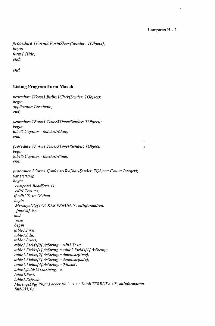
procedure TForm2.FormShow(Sender: TObject); begin forml.Hide; end;
end.
Listing Program Form Masuk
procedure TFormi.BitBtni Click(Sender: TObject); begin application. Terminate; end;
procedure TFormi.Timer2Timer(Sender: TObject); begin label5. Caption: =datetostr(date); end;
procedure TFormi.Timer3Timer(Sender: TObject); begin label6. Caption: =timetostr(time); end;
procedure TFormi.ComPortlRxChar(Sender: TObject; Count: integer); var s: string; begin
comportl.ReadStr(s, I); editl. Text: =s; if editl. Text= '9' then begin MessageDlg(LOCKER PENUH!II', mtlnformation, [mbOkj,O);
end else
begin fable I. First; table I. Edit; table I.Insert; table i.Fields [OJ.AsString: =edit2. Text; table 1. Fie Ids {l j.AsString: =table 2.Fields [1 j .AsString; fable i. Fields [2 j AsString: =timetostr(time); table i.Fields [3 j.AsString: =datetostr(date); table I. Fields [4 j.AsString: = 'Masuk'; table i.fields [5 j.asstring: =s; table I . Post; table i.Refresh; MessageDlg(Pintu Locker Ke '+ s + 'Telah TERBUKA "I', mtlnformation, [mbOkj,O);
Lampiran B-2
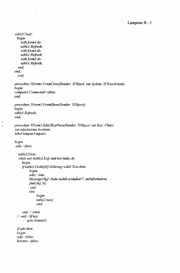
edit2.Clear; begin
with form4 do tablel.Refresh; with form3 do tablel.Refresh; with form5 do tablel.Refresh;
end; end;
end;
procedure TFormIFormClose(Sender: TObject; var Action: TCloseAction); begin comportl.Connected:=false; end;
procedure TForml.FormShow(Sender: TObject); begin tablel.Refresh; end;
procedure TForml.Edit2KeyPress(Sender: TObject; var Key: Char); var ada,ketemu: boolean; labellompat,lompat2;
begin ada: =false;
table2.First; while not (table2.Eoj) and not (ada) do
begin if table2.Fields[0 j.AsString=edit2. Text then
begin ada:=true; MessageDlg(' Anda sudah terdaftarl I', mtln/ormation, [mbOkj,O); end
else begin table2.next; end;
end; llwhile II end; Ilifkey
il goto lompat2;
ifada then begin ada:~alse;
ketemu: =false;
Lampiran B-3

table] .First; while not (tableI.Eoj) and not(ada) do
begin if ((tableI.Fields[O j.AsString=edit2. Text)) then begin
ada:=trne; if (table 1. Fields[ 4 ).AsString= 'Mas uk') then
begin MessageD/g(' Anda sudah punya loker! I', mtInformation, [mbOkj,O); ketemu:= true;
end else
begin
end else begin
MessageDIg(,Anda mall kelllar1f', mtlnformation, [mbOkj,O); ketemll:= false;
end
tableI.next; end;
end; j1while if not(ketemu) then
begin
end; end;
end.
messageDIg(' Anda Belum AKSESII', mtlnformation, [mbOkj,O); comportl. WriteStr(#65);
end;
Listing Program Form Perpanjangan
procedure TForm3. Timer 1 Timer(Sender: TObject); begin labell . Caption: =datetostr(date); end;
procedure TForm3. Timer2Timer(Sender: TObject); begin label2. Caption: =timetostr(time); end;
procedure TForm3.Edit1KeyPress(Sender: TObject; var Key: Char); begin edit2. Text: =copy(editl. Text, 1 ,1 0); end;
Lampiran B - 4

procedure TForm3.Edit2Change(Sender: TObject); begin table i.First; while not (tablei.Eof) do
begin if table i.Fields[0j.AsString=edit2. Text then
begin 15. Caption: =table1.Fields[5 j.AsString; label5. Caption: =table1.Fields [1 J .AsString; comport2. WriteStr(chr(strtoint(l5.Caption) + 48)); table i.First; table 1. Edit; table] .Insert; table i.Fields[Oj.AsString: =edit2. Text; tablei.Fields[l j.AsString: =labeI5.Caption; table 1. Fields[2 j.AsString: =timetostr(time); table 1. Fields [3 j.AsString: =datetostr(date); table1.Fields[4j.AsString:='Perpanjangan'; table 1. Fields [5 j.AsString: =15.Caption; tablei.Post; table i.Refresh;
Lampiran B - 5
MessageDlg(Locker Ke '+ 15.caption +' Telah TERBUKA!!!.'. mt1nformation. [mbOkJ.O);
end;
edit2.Clear; break;
end else begin
table i.Next; end;
begin withform1 do table i.Refresh;
withform4 do table i.Refresh;
withform5 do table] .Refresh;
end; end;
procedure TForm3.FormClose(Sender: TObject; var Action: TCloseAction): begin comport2.Connected: =false; end;

procedure TForm3.FormShow(Sender: TObject); begin tablel.Refresh; end;
end.
Listing program Form Keluar
procedure TForm4.TimerITimer(Sender: TObject); begin label3. Caption: =datetostr(date); end;
procedure TForm4.Timer2Timer(Sender: TObject); begin label4. Caption: =timetostr(time); end;
procedure TForm4.Edit2Change(Sender: TObject); begin
table I.First; while not (tablel.Eof) do
begin if table 1. Fields [0 j.AsString=edit2. Text then
begin
labeI5.Caption: =tableJ .Fields[5 j.AsString; label6. Caption: =table 1. Fields [I j.AsString; comport3. WriteStr(chr(strtoint(labeI5. Caption) +48)); tablel·first; tablel.Insert; table 1. Fields[Oj.A sString: =edit2. Text; table 1. Fields[I j.AsString: =labeI6.Caption; table 1. Fields [2 j.AsString: =timetostr(time); table I. Fields [3 j .AsString: =datetostr(date); table 1. Fields [4 j.AsString: = 'Keluar'; table I. Fields[5 j.AsString: =labeI5.Caption; tableI.Post; table I. Refresh;
Lampiran B - 6
MessageDlg('Pintu Locker Ke '+ label5.Caption + 'Telah TERBUKA I,,', mtlnformation.[mbOkj, 0); edit2.Clear; {close;} break; end else begin

end;
tableI.Next; end; end; begin withformI do table I.Refresh; withform3 do table] .Refresh; with form5 do tableI.Refresh; end;
procedure TForm4.FormClose(Sender: TObject; var Action: TCloseAction); begin comport3. Connected: ~false; end;
procedure TForm4.FormShow(Sender: TObject); begin tableI.Refresh; end;
Lampiran B - 7

Lampiran C- I
$incIude(reg51.inc) '*********************************************************************** , ;PROGRAM ASSEMBLY PERANCANGAN DAN PEMBUATAN LOKER OTOMATIS .*********************************************************************** ,
mulai:
org OOh ajmp mulai org 60h
;Program dimulai pada alamat OOh
mov pO,#OOOOOOOOb mov pI ,#Offh acall inisial
ulang: mov jnb clr mov cjne ajmp
a,#OOh ri,cekl ;cek ke limit switch n a,sbuf a,#41h,lopl pintul
,--------------------------------------------;ini uutuk mengecek limit switch ;--------------------------------------------------------.--------------------------------------------------cekl: jub pl.O,cek2
cJrpO,O
cek2: jub pl.l,cek3 elr pO. I
~ek3: jnb p 1.2,cek4 clrpO.2
!k4: jub p1.3,cek5 clr pOJ
k5: jub p 1.4,eek6 elr pOA
I
I
I
I
I
I
I
I
I
I

cek6: jnb pl.S,cek7 c1rpO.5
cek7: jnb pl.6,cek8 clrpO.6
cek8: jnb p 1.7 ,balik clrpO.7
balik: ajmp ulang
pintul: jnb p2.0,bukal ajmppintu2
bukal: setb pO.O mov a,#3lh acall kirim ajmp ulang
pintu2: jnb p2.1 ,buka2 ajmp pintu3
buka2: setb pO. 1 mova,#32h acall kirim ajmp ulang
pintu3: jnb p2.2,buka3 ajmppintu4
buka3: setb pO.2 mova,#33h acall kirim ajmp ulang
lopl: ajmp doorl
Lampiran c- 2
;cek sensor apa p2.0 ada barang kalau tidak ada lompat ke bukal ;tidak ada barang lompat ke pintu2
;buka solenoidl ; pindah isi 3lh ke A ;panggil kirim ;lompat keulang
;cek sensor apa p2.1 ada barang kalau tidak ada lompat ke buka2 ;tidak ada barang lompat ke pintu3 ;aktifkan solenoid2 ;pindahkan isi32h ke A
;cek sensor apa p2.2 ada barang kalau tidak ada lompat ke buka3
pintu4: jnb p2.3,buka4 ;cek sensor apa p2.3 ada barang kalau tidak ada lompat ke buka4 ajmp pintuS
buka4: setb pO.3 mova,#34h acall kirim ajmp ulang
pintuS: jnb p2.4,bukaS ;cek sensor apa p2.4 ada barang kalau tidak ada \ompat ke buka5

ajmp pintu6
buk:aS: setb pO.4 mova,#3Sh acall kirim ajmp ulang
Lampiran C- 3
pintu6: jnb p2.5,buka6 ;cek sensor apa p2.S ada barang kalau tidak ada lompat ke buk:a6 ajmppintu7
buka6: setb pO.S mova,#36h acall kirim ajmp ulang
pintu7: jnb p2.6,buka7 ;cek sensor apa p2.6 ada barang kalau tidak ada lompat ke buka7 ajmp pintu8
buka7: setb pO.6 mova,#37h acall kirim ajmp ulang
pintu8: jnb p2.7,buka8 ;cek sensor apa p2.7 ada barang kalau tidak ada lompat ke buka8 ajmp kirim_berita ;mengirim data ke delphi
buka8: setb pO. 7 mov a,#38h acall kirim ajmp ulang
-------------------------------------------------------------------------------------------------------------, ; Perintah untuk mengirim data ke Delphi ,-------------------------------------------------------------------------------------------------------------
kirim _ berita: mov a,#39h acall kirim ;mengirim data ajmp ulang
jauh: aJmp ulang
"-------------------------------------------------------------------------------------------------------------, ;perintah untuk keluar atau memperpanjang loker -------------------------------------------------------------------------------------------------------------,
doorl: CJne a,# 31 h,door2 setb pO.O aJmp ulang
door2: CJne a,#32h,door3
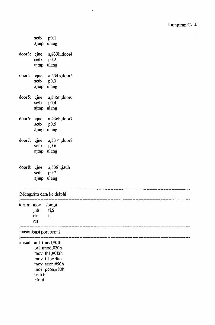
Lampiran C- 4
setb pO.1 aJmp ulang
door3: CJne a,#33h,door4 setb pO.2 aJmp ulang
door4: cJne a,#34h,door5 setb pOJ aJmp ulang
door5: cJne a,#35h,door6 setb pO.4 aJmp ulang
door6: CJne a,#36h,door7 setb pO.5 aJmp ulang
door7: cJne a.#37h,door8 setb 90.6 aJmp ulang
door8: CJne a,#38hjauh setb pO.7 aJmp ulang
,-------------------------------------------------------------------------------------------------------------;Mengirim data ke delphi ,-----------------------------------------------------------------.-------------------------------------------kirim: mov
jnb elf ret
sbuf,a ti,$ ti
,-------------------------------------------------------------------------------------------------------------;inisialisasi port serial ,-------------------------------------------------------------------------------------------------------------inisial: anI tmod,#Oth
orl tmod,#20h mov th I ,#Ofab mov tll ,#Ofah mov scon,#50h mov pcon,#80h setb trl elf ti

clr ri ret end
Lampiran C- 5
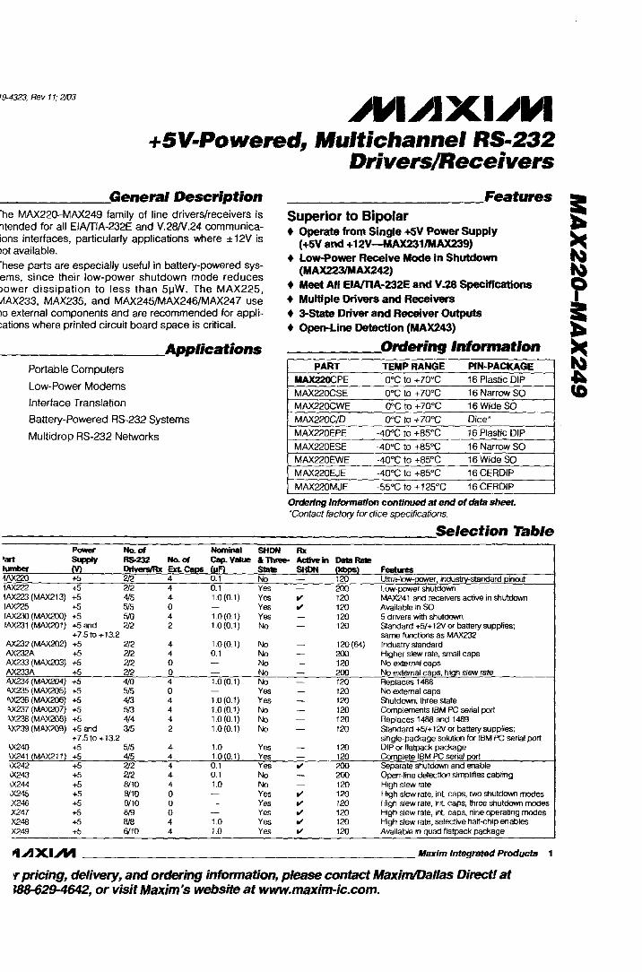
1~23; Rev 11; 2/03
~~I"'JXI~~I +5V-Powered, Multichannel RS-232
Drivers/Receivers ____________ ~GeneraIOescription The MAX220--MAX249 family of line drivers/receivers is intended for all EINTIA-232E and V.28/V.24 communications interfaces, particularly applications where ± 12V is not available. These parts are especially useful in battery-powered systems, since their low-power shutdown mode reduces power dissipation to less than 5/lW. The MAX225, MAX233, MAX235, and MAX245/MAX246/MAX247 use no external components and are recommended for applications where printed circuit board space is critical.
__________________ AppHcations Portable Computers
Low-Power Modems
Interface Translation
Sattery-Powered RS-232 Systems
Multidrop RS-232 Networks
Power No. 01 Nominal stiCH
______________________ Features Superior to Bipolar • Operate from Single +5V Power Supply
(+5V and +12V-MAX231JMAX(39) • Low-Power Receive Mode in Shutdown
(MAX22l1MAX242)
• Meet All EIAITlA.-232E and V.28 Specifications • MuHlple Drivers and Receivers • 3-State Driver and Receiver OUtputs • Open-Line Detection (MAX243)
Ordering 'aformation PART TEMP RANGE PIN-PACKAGE
MAX220CPE O°C to +70°C 16 Plastic DIP
MAX220CSE OOC to +70°C 16 Narrow SO
MAX220CWE OOC to +70°C 16 Wide SO
MAX220C/D O°C to + 70"C Dice'
MAX220EPE -400C to +85°C 16 Plastic DIP
MAX220ESE -40°C to +85°C 16 Narrow SO
MAX220EWE -40"C to +85°C 16 Wide SO
MAX220EJE -40°C to +85°C 16CERDIP
MAX220MJE -55°C to +125°C 16CERDIP
Ordering Information continued at end of data sheet. 'Contact factory for dice specifICations.
Selection Table Ax
'art ~oppI)' flS.232 No. 01 Cap. Value a_ _ in Data Ra1e
DoiventlRx Ext. Ca~ 1I,f} lumber SIa1e SHDH (kbps) features IAX220 +5 212 4 0.1 No 120 UItra-Iow-jlOWer, induslrJ'-S..tandard oinout 1= +5 212 4 0.1 Yes 200 LOoN-power shutdown IAXm (MAX213) +5 4/5 4 1.0(0.1) Yes t/' 120 WJ<241 and receivers active in shlJtda.Nn IAX225 +5 5/5 0 - Yes t/' 120 Available in SO IAX230 (MAX200) +5 5/0 4 1.0 (0.1) Yes - 120 5 drivers with shutdoYin 1AX231 (MAX201) +5 and 212 2 1.0(0.1) No - 120 Standard +S/+ 12V or battery supplies;
+7.5 to + 13.2 same functions as MAX232 IAX232 (MAX202) +5 212 4 1.0(0.1) No - 120(64) Industry standard AX232A +S 212 4 0.1 No - 200 Higher slew rate, small caps AX233 (MAX203) +5 212 0 - No - 120 No external caps AX233A +S 212 0 - No 200 No external caps high slew rate AX234 (MAX204) +5 4!tl 4 1.0(0.1) No 120 Replaces 1488 1\)(235 (MAX20S) +S 5/5 0 - Yes - 120 No extemal caps 'IX236 (MAX206) +5 413 4 1.0(0.1) Yes - 120 Shutdown, three state '1)(237 (MAX207) +5 S!3 4 1.0(0.1) No - 120 Complements IBM PC serial port 'IX238 (MAX208) +S 4/4 4 1.0(0.1) No - 120 Replaces 1488 and 1489 'IX239 (MAX200) +S and 3/5 2 10(0.1) No - 120 Standard +5/+ 12V or battery &Jpplies;
+7.5 to + 13.2 single-package solution for IBM PC serial port \)(240 +5 5/5 4 1.0 Yes - 120 DIP or "a!pack package \)(241 (MAX211) +5 4/5 4 1.0 (0.1) Yes - 120 Com.Jllete IBM PC serial port 1)(242 +S 212 4 0.1 Yes t/' 200 Separate shutdown and enable \X243 +5 212 4 0.1 No - 200 Open-line detectlor1 simplifies cabling 0(244 +5 8110 4 1.0 No - 120 High slew rate '><245 +S 8110 0 - Yes t/' 120 f-figh slew rate, lnt caps, two shutcfolM1 modes .><246 +5 8110 0 - Yes t/' 120 High slew rate, lnt caps, ttlree shutdown modes X247 +5 8!9 0 - Yes t/' 120 High slew rate, int caps, nine operating modes X24B +S B/8 4 1.0 Yes t/' 120 High slew rate, selective half-chip enables X249 +5 6/10 4 1.0 Yes t/' 120 Available in quad flatpack: package
".AXIAIII _________________________ Maxim Integrated Products
'r pricing, delivery, and ordering information, please contact Maxim/Dallas Direct/ at UlB-629-4642, or visit Maxim's website at www.maxim-ic.com.

+5V·Powered, Multichannel RS·232 Drivers/Receivers
ABSOLUTE MAXIMUM RATINGS-MAX22012221232A1233A12421243 Supply Voltage (Vee) .. Input Voltages
.. ..... ·0.3V to +6V 20-Pin Plastic DIP (derate 8.00mW/"C above +70OC) ..44OmW
TIN .......... .. RIN (Except MAX220) . RIN (MAX220) ... TOUT (Except MAX220) (Note 1). TOUT (MAX220) ....
Output Voltages
.... -0.3V to (Vee - 0.3V) .. ............ ±30V
. ................. ±2SV .............. ±1SV ............ ±13.2V
16-Pin NarrON SO (derate 8.7OmW/"C above +700c) ... 696mW 16-Pin Wide SO (derate 9.S2mWfC above +70OC) ...... 762mW 18-Pin Wide SO (derate 9.52mWfC above +70OC) .... ..762mW 20-Pin Wide SO (derate 10.0OmW/"C above + 70"C) ... .8oOmw 20-Pin SSOP (derate 8.00mW/"C above +70°C) .......... 64OmW 16-Pin CERDIP (derate 10.00mW/"C above + 70°C) ..... 80OmW 18-Pin CERDIP (derate lO.S3mW/"C above + 70"C) ..... B42mW
TOUT.... .. .. ±1SV Operating Temperature Ranges ROUT.. .. ......................................... -0.3V to (Vee + 0.3V) MAX2... ..AC __ . MAX2 __ C __ ............................. O"C to +70°C
Driver/Receiver Output Short Circuited to GND ......... Continuous MAX2... _AE __ . MAX2 __ E __ .......................... -40"C to +85°C Continuous Power Dissipation (T A = +70°C) MAX2.....AM __ . MAX2 __ M __ ....................... -55°C to +12SoC
16-Pin Plastic DIP (derate 10.53mW/"C above +70"C) .... B42mW Storage Temperature Range .................... ..·65°C to + 160°C 18-Pin Plastic DIP (derate 11.11mWrC above +70OC) .... 889mW Lead Temperature (soldering. 108).............. . .. +300°C
Note 1: Input voltage measured with TOUT in high-impedance state. SHDN or Vee = OV. Note 2: For the MAX220. V+ and V- can have a maximum magnitude of 7V. but their absolute difference cannot exceed 13V. Stresses beyond those listed under ~ Absolute Maximum Ratings" may cause permanent damage to the deVice. These are stress ratings only, and functional operation of the device at these or any other conditions beyond those indicated in the operational sections of the specifications is not implied. Exposure to absolute maximum rating conditions for extended periCKis may affect device reliability.
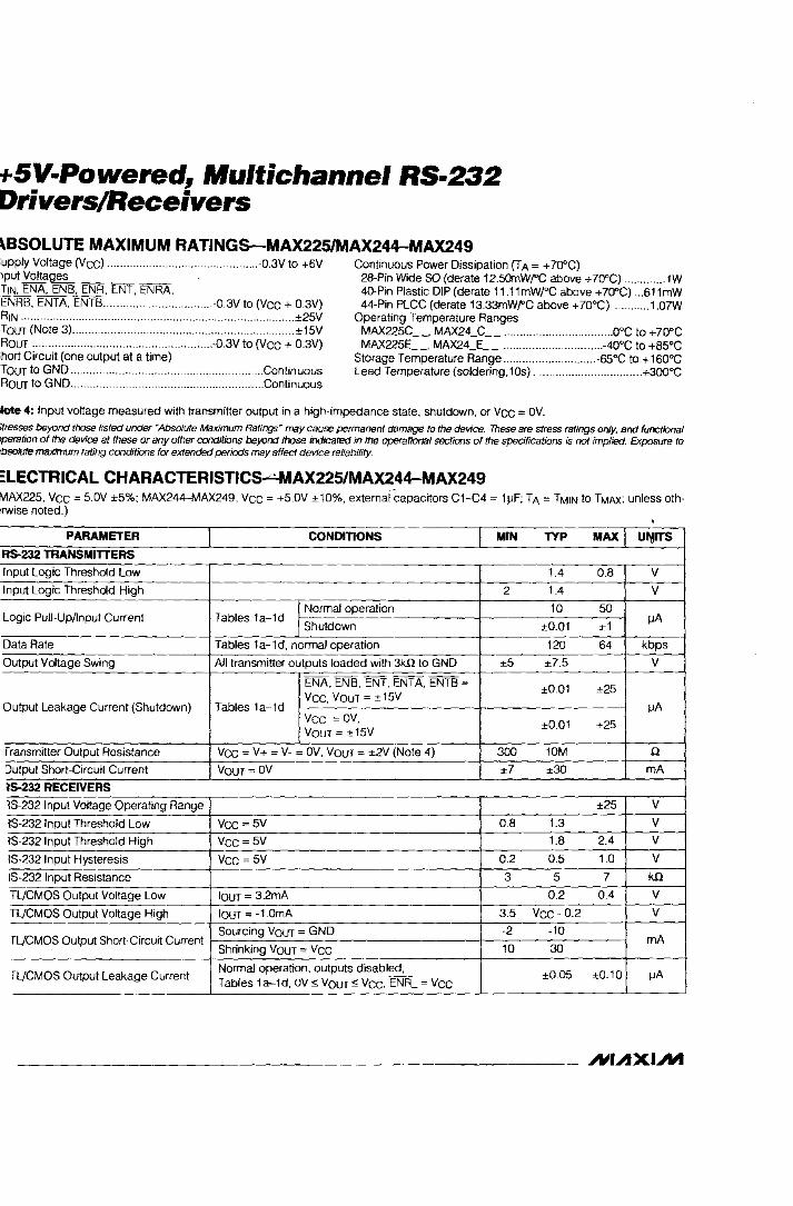
ELECTRICAL CHARACTERISTICS-MAX22OI222I232A1233A12421243 Vee = +sv ±10%. C1-C4 = 0.1~F. MAX220. C1 = a.a47~F. C2~4 = a.33~F. TA = TMIN to TMAX. unless otherwise noted.)
PARAMETER CONDITIONS MIN TYP MAX UNITS
RS-232 TRANSMITTERS
Output Voltage Swing All transmitter outputs loaded wtth 3ill to GND ±S ±8 V
Input Logic Threshold Low 1.4 0.8 V
I nput Logic Threshold High All devices except MAX220 2 1.4
MAX220: Vee = S.OV V
2.4
Logic Pull-Up/Input Current All except MAX220. normal operation S 40
SHDN ~ av. MAX222/242. shutdown. MAX220 ±0.01 ±1 ~A
Jutput Leakage Current Vee = S.5V. SHDN = OV. VOUT = ±15V. MAX222/242 ±0.01 ±10
Vee = SHDN = OV. VOUT = ± 15V ±0.01 ±10 jJA
Jata Rate 200 116 kbps
ransmitter Output Resistance Vee ~ V+ ~ V- = OV. VOUT = ±2V 300 10M n Jutput Short-Circuit Current VOUT = OV ±7 ±22 mA
18-232 RECEIVERS
IS-232 Input Voltage Operating Range ±30 V
S-232 Input Threshold Low Vee = SV All except MAX243 R21N 0.8 1.3
V MAX243 R21N (Note 2) ·3
S-232 Input Threshold High Vee~SV All except MAX243 R21N 1.8 2.4
V MAX243 R21N (Note 2) -O.S -0.1
,·232 Input HystereSis All except MAX243. Vee ~ SV. no hysteresis in shdn. 0.2 O.S 1
V MAX243 1
,-232 Input Resistance 3 5 7 kU
'L/CMOS Output Voltage Low lOUT = 3.2mA 0.2 0.4 V
L/CMOS Output Voltage High lOUT - -1 .omA 3.S Vee - 0.2 V
Sourcing Your ~ GND -2 -10 L/CMOS Output Short-Circurt Current mA
Shrinking Vour = Vee 10 30
________________________ .MAXI""

+5V-Powered!l Multichannel RS-232 Drivers!Receivers
ELECTRICAL CHARACTERISnCs-MAX22012221232A1233A12421243 (continued) (Vee=+5V±10% Cl--C4=O.I~F,MAX220,Cl =0.047~F C2-C4=033~F TA=TMINtoTMAX unlessotherwisenoted)
PARAMETER CONDITIONS MIN TYP MAX UNITS
TT[JCMOS Output Leakage Current SHDN = Vee or EN = Vee (SHDN = OV for MAX222), ±0.05 ±1D ~A OV" VOUT " Vee
EN Input Threshold Low MAX242 1.4 0.8 V
EN Input Threshold High MAX242 2.0 1.4 V
Operating Supply Vokage 4.5 5.5 V
No load MAX220 0.5 2
Vee Supply Current (SHDN = Vee), MAX222/232A/233A/242/243 4 10 rnA
Figures 5. 6.11.19 3k1110ad MAX220 12 both inputs MAX222J232A/233A/242J243 15
TA = +25°C 0.1 10
Shutdown Supply Current MAX222J242 TA = DoC to +70°C 2 50
TA = -400C to +85°C 2 50 ~A
TA = -55°C to + 125°C 35 100
SHDN Input Leakage Current MAX222J242 ±1 ~A
SHDN Threshold Low MAX222/242 1.4 0.8 V
SHDN Threshold High MAX222/242 2.0 1.4 V
CL = 50pF to 2500pF, MAX222J232A/233A/242/243 6 12 30 RL = 3kU to 7k.u.
Transition Slew Rate Vee = 5V. TA = +25OC. V/~s measured from +3V MAX220 1.5 3 30 to -3V or -3V to +3V
MAX222/232A/233A/242/243 1.3 3.5 Transmrtter Propagation Delay tpHLT
MAX220 4 10 TLL to RS-232 (Normal Operation).
MAX222/232A/233A/242/243 1.5 3.5 ~s
Figure 1 tpLHT MAX220 5 10
MAX222/232A/233A/242/243 0.5 1 Receiver Propagation Delay tpHLR
MAX220 0.6 3 RS-232 to TLL (Normal Operation).
MAX222J232A/233A/242J243 0.6 1 ~s
Figure 2 tpLHR MAX220 0.8 3
Receiver Propagation Delay tpHLS MAX242 0.5 10
~S-232 to TLL (Shutdown). Figure 2 MAX242 2.5 10 ~s
tpLHS
~eceiver-Output Enable Time. Figure 3 tEA MAX242 125 500 ns
~eceiver-Output Disable Time. Figure 3 tDR MAX242 160 500 ns
-ransrnrtter-Output Enable Time tET
MAX222/242, O.I~F caps 250 ~s SHDN Goes High). Figure 4 (includes Charge-pump start-up)
'ransmrtter-Output Disable Time tDT MAX222/242. O. 1 ~F caps 600 ns
SHDN Goes Low), Figure 4
ransmrtter + to - Propagation MAX222/232A/233A/242/243 300 tpHL T - tPLHT ns
lelay Difference (Normal Operation) MAX220 2000
eceiver + to - Propagation MAX222/232A/233A/242/243 100 tpHLR - tPLHR ns
'elay Difference (Normal Operation) MAX220 225
,te 3: MAX243 R20UT is guaranteed to be low when R21N is;, OV or is floating
3
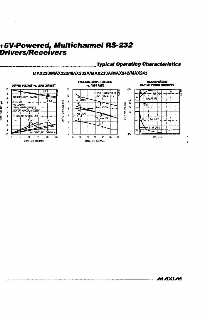
+5V.Powered, Multichannel RS·232 Drivers/Receivers _________________ 'JYpical Operating Characteristics
MAX2201MAX222JMAX232A1MAX233A1MAX2421MAX243
10
8
6
~ 2 g 0 ~
~ -2 ~
a -4
-6
-8
-10
UUl'PUT VtllTASE YS. LOAD CU1111E1T
l~FJ
E1lHER Y+ OR vlOADED
vcc=t5V o.l~ '-NO LOAD ON I IHANSMlmn OUlPlJTS (EXCEPT MAX22Il, MAX233A)
I I I v- LOADED, NO LOAD ON v+ ,
o~ ~-~
V+ LOADED, NO LOAD ON V
o 10 15 20 25
LOAD CURRENT (mA)
11
10
'" .s 9 ~
i5 8 or or ~ u ~ 7 ~ ~ ~ ~ a 6
AVAUIU OUTPUT ClllIIBIT YS. DATA RATE
10 20 m ~ ~ 00
DATA RAIf (kbils/",,)
+lOV
+5V 2+5V ~
'" OV ;5
~ OV 0< .->
-lOV
V+ I-
v-
MAX222IIIAX242 U .. nME EXm. SIIUTOOWI
.....,. -'1~CAPi V+
~ ~ol~C~ i ID[
\-0 - 1ri \ t+ ~OJ~FCAPS
v-'-f-r-+-.L
5OO~S/div
.MAXIAt

+5V.Powered, Multichannel RS·232 Drivers/Receivers
ABSOLUTE MAXIMUM RATINGS-MAX2231MAX23o-MAX241 Vee ................ _ ................................ · ............ _ .. -0.3V to +6V
... (Vee - O.3V) to + 14V V+ V- ............ .. Input Voltages TIN .. RIN .......... ..
Output Voltages
.. ............ +0.3Vto -14V
. ......... -0.3V to (Vee + 0.3V) .. ............. ±30V
TOUT ... .. ............................. (V+ + 0.3V) to (V- - 0.3Y) ROUT.. ...... ........... .. ... -O.3V to (Vee + O.3Y)
Short-Circutt Duration, TOUT ...... .. ....... Continuous Continuous Power Dissipation (T A ~ + 70°C)
20-Pin Wide SO (derate 10 OOmWfC above + 70°C) ...... 80OmW 24-Pin Wide SO (derate 11.76mWfC above +70"C) ....... 941mW 28-Pin Wide SO (derate 12.5OmWfC above +70°C) ....... _ ..... lW 44-Pin Plastic FP (derate 11.11mWfC above +700C) ..... 889mW 14-Pin CERDIP (derate 9.00mwfC above +70°C) .......... 727mW 16-Pin CERDIP (derate 10.00mWfC above +700C) ........ 800mW 20-Pin CERDIP (derate 11.11mWfC above +700C) ........ B89mW 24-Pin Narrow CERDIP
(derate 12.5OmWfC above +700C) .............. 1W 24-Pin Sidebraze (derate 20 OmW/"C above +70°C) .......... 1.6W 2B-Pin SSOP (derate 9.52mW/oC above +70"C) ....... _ ..... 762mW
14-Pin Plastic DIP (derate 10.00mwfC above +700C) .... 800mW Operating Temperature Ranges 16-Pin Plastic DIP (derate 10.53mWfC above +70'C) ... .B42mW MAX2 __ C __ ...................... . ................... O°C to +70°C 2O-Pin Plastic DIP (derate 11.11mWfC above +700C) .... BB9mW MAX2 E ............. -40°C to +B5°C 24-Pin Narrow Plastic DIP MAX2 __ M __ ................ . ............... -55°C to +125'C
(derate 13.33mWfC above +70°C) ......... 1.07W Storage Temperature Range ........................... _65°C to +l60°C 24-Pin Plastic DIP (derate 9.09mWfC above +70°C) ..... 500mW Lead Temperature (soldering, lOs) ................................ +300°C 16-Pin Wide SO (derate 9.52mWI'C above +70°C) ....... 762mW
Stresses be}OOd those listed under "Absolute Maximun Ranngs" may cause permanent damage to the device. These are stress ratings only, and functional operation of the device at these or any other conditions beyond those indicated in the operational sections of the specifications ;s not implied. Exposure to absofute ma>dmum rating CfX1ditions for extended pericx:Js may affect device reliability.
ELECTRICAL CHARACTERISTICS-MAX2231MAX23O-MAX241 (MAX223/230/232/234/236/237/238/240/241, Vee ; +5V ±10; MAX233/MAX235, Vee ~ 5V ±5%, Cl-C4 ~ 1.0~F; MAX231/MAX239, Vee ~ 5V ±10%; v+ ~ 7.5V to 13.2V; TA ~ TMIN to TMAJC unless otherwise noted.)
PARAMETER CONDITIONS MIN TYP MAX UNITS
Output Voltage Swing All transmitter outputs loaded wtth 3k.O. to ground ±5.0 ±7.3 V
MAX232/233 5 10
Vee Power-Supply Current No load,
MAX223/230/234-23B!240/241 7 15 rnA TA ~ +25°C
MAX231/239 0.4 1
V+ Power-Supply Current MAX231 1.B 5
rnA MAX239 5 15
Shutdown Supply Current MAX223 15 50
TA = +25'C MAX230/235/236/240/241
~A 1 10
Input Logic Threshold Low TIN; EN, SHDN (MAX233); EN, SHDN (MAX230/235-241) O.B V
TIN 2.0
Input Logic Threshold High EN, SHDN (MAX223); V
EN, SHDN (MAX230/235/236/240/241) 2.4
Logic Pull-Up Current TIN=OV 1.5 200 ~A
Receiver Input Voltage -30 30 V
Operating Range
MAXIM 5

+5V.Powered, Multichannel RS·232 Drivers!Receivers
ELECTRICAL CHARACTERISTICS-MAX2231MAX23O-MAX241 (continued) (MAX223/230/232/234/236/237/238/240/241. Vee = +5V ±10; MAX2331MAX235. Vee = 5V ±5%. C1-C4 = 1.0~F; MAX231IMAX239. Vee = 5V ±10%; v+ = 7.5V to 13.2V; TA = TMIN to TMAX; unless otherwise noted.)
PARAMETER CONDITIONS MIN TYP MAX UNITS
Normal operation SHDN = 5V (MAX223) 0.8 1.2
TA = +25°C. SHDN = OV (MAX235/236/240/241) RS-232 Input Threshold Low
Vee = 5V V Shutdown (MAX223)
SHDN =OV. 0.6 1.5 EN = 5V (R4IN. R5IN)
Normal operation SHDN = 5V (MAX223) 1.7 2.4
TA = +25°C. SHDN = OV (MAX235/236/240/241) RS-232 Input Threshold High V
Vee = 5V Shutdown (MAX223) SHDN =OV. 1.5 2.4 EN = 5V (R4IN. R5IN)
RS-232 Input Hysteresis Vee = 5V. no hysteresis in shutdown 0.2 0.5 1.0 V
RS-232 Input Resistance TA = +25°C. Vee = 5V 3 5 7 k.Q
nUCMOS Output Vo~age Low lOUT = 1.6mA (MAX231/232/233. lOUT = 3.2mA) 0.4 V
nUCMOS Output Vo~age High lOUT = -1mA 3.5 Vee - 0.4 V
nUCMOS Output Leakage Current OV 5 ROUT 5 Vee; EN = OV (MAX223);
0.05 ±10 IJA EN = Vee (MAX235-241 )
Normal MAX223 600 Receiver Output Enable Time
operation ns
MAX235/236/239/240/241 400
Normal MAX223 900 Receiver Output Disable Time ns
operation MAX235/236/239/240/241 250
RS-232IN to Normal operation 0.5 10
Propagation Delay nUCMOSOUT. SHDN=OV tpHLS 4 40 IJs CL = 150pF (MAX223) tpLHS 6 40
MAX223/MAX230/MAX234-241. TA = +25°C. Vee = 5V. RL = 3k.Q to 7k.Q. CL = 50pF to 2500pF. measured from 3 5.1 30 +3V to -3V or -3V to +3V
V/~s Transition Region Slew Rate MAX231/MAX232/MAX233. TA = +25°C. Vee = 5V. RL = 3k.Q to 7k.Q. CL = 50pF to 2500pF. measured from 4 30 +3V to -3V or -3V to +3V
Transmitter Output Resistance Vee = V+ = V- = OV. VOUT = ±2V 300 n
Transmitter Output Short-Circuit Current
±1D mA
6

+5V-Powered, Multichannel RS-232 Drivers/Receivers
________________ l'ypical Operating Characteristics
MAX223JMAX23~MAX241
8.5
8.0
~ ~ 75 g
7.0
6.5
-6.0
-6.5
-7.0
~
~ -7.5
-8.0
-8.5
-9.0
4.5
4.5
T1IAIISMITTER OUTPUT VOLTAIE (v1IIII 15. Vee
5.0 Vee (V)
TRAIISMITTER OUTPUT VOLTAIE (Va) I$. Vee
5.0
VeeM
.M.AXI.M
7.4
7.2
7.0
~ 6.8 ~
g 6.6
6.4
6.2
6.0 5.5
-6.0
-6.2
-6.4
·6.6 ~
:!" -6.8
-7.0
-72
-7.4
-7.6 5.5
T1IAIISMITTBI OUTPUT VOLTAIE (vUIII I$. LOAD CAPACITAICE AT
DIFFERUT DATA RATES
......... 1"-- V
l»<-v-< 1"-.... 1601<bilslsec / V f\. 6OI<bilsisec 2Okbi~sec
\ I TA:+25°C vee =+5V 1\ 3 TRANSMITT£RS lOADED At dkll I CH4:1111' \
i
500 1000 1500 2000 2500
lOAD CAPACITANCE (pF)
TRAlSlllTTEII OUTPUT VOLTAGE (Va) , I$. lOAD CAPACITAIICE AT
DlFFEREIT DATA RATES
T,:+25°C ~
f-Vee =+5V / f- ~ TRANSMITT£RS lOADED
Rl=3kn I / C1-C4-1111'
1~bilSIsec I / f-- 8Okbilslsoc ~ ./ ~ 2VKkbils/sec
/~ V ...... V./ V "'" ~ o 500 1000 1500 2000 2500
lOAD CAPACITANCE (pF)
V+, V· WHEI EXm .. SIRITDDWI 11!!F CAPACl11IIIS)
500msJdiv
·SHUIDOWN POlARITY IS REVERSED FOR NON MAX241 PARTS
12.0
11.0
10.0
~ ~ 9.0
~ 8.0
~ 7.0 w
~ 0> +' >
6.0
5.0
4.0
10
4
2
-2
-4
-6
-8
-10
TRAlSlllTTER Sl£W RATE IS. LOAD CAPACITAICE
o 500 1000 1500 2000 2500 lOAD CAPACITANCE (pF)
T1IAIISMITTBI OUTPUT VOL TAlE (V+, V·) IS. LOAD CIIRIIEIT
I ~
~ T-+-.:j T,_+25°C if f..
I- VCC=+5V C1-C4= 1~F
V+ANOV· V-lOADED, V+ lOADED,
EQUAllY - NO lOAD I-ONV+ NO lOAD
lOADED ON V- -~ I
1/ tI.- l. J.,.
~ ~ I-..... AlllllANSMlTTERS UM.OADED
o 5 10 15 m ~ ~ ~ ~ ~ ~ CURRENT (mA)
7
+SV·Powered, Multichannel RS·232 Drivers!Receivers
ABSOLUTE MAXIMUM RA TINGS-MAX225IMAX244-MAX249 Supply Voltage (Vee) .................... . ..... -0.3V to +6V Continuous Power Dissipation (T A = + 70°C) Input Volla~ _____ _
T,N, ENA, ENB, ENR, ENT, ENRA. 28-Pin Wide SO (derate 12.5OmWf'C above +7QOC) ............. IW
ENRB, ENTA. ENTB..... . .. ... -0.3V to (Vee + 0.3V) 40-Pin Plastic DIP (derate 11.llmWrC above +700C) ... 611mW
R'N ..................... ................................. .. ........... ±25V 44-Pin PLCC (derate 13.33mWf'C above +70°C) .......... 1.07W
Operating Temperature Ranges TOUT (Note 3)..... .. ............ ± 15V MAX225C __ , MAX24_C __ . . .... O°C to +70°C ROUT ...................................................... -0.3V to (Vee + 0.3V) MAX225E __ , MAX24_E __ .............................. -40°C to +85°C
Short Circuit (one output at a time) TOUT to GND.. . .... Continuous
Storage Temperature Range ............................ -65°C to + 1600C Lead Temperature (soldering, 1 Os) ... .. +300°C
ROUT to GND.. .. .. Continuous
Note 4: Input vo~age measured with transmitter output in a high-impedance state, shutdown, or Vee = OV.
Stresses beyond those listed under ~Abso/ute Maximum Ratings" may cause permanent damage to the device. These are stress ratings only, and functional operation of ItJe device at (fJese or any o(fJer conditions be}<Jnd lhose indicated in ItJe operalionaf sections of ItJe specificaffons is not implied. Exposure to absoltJte maximum rating conditions for extended periods may affect device reliability.
ELECTRICAL CHARACTERISTICS"""-MAX225/MAX244-MAX249 MAX225, Vee = 5.0V ±5%; MAX244-MAX249, Vee = +5.0V ±10%, external capaCITors Cl-C4 = lJ.lF; TA = TMIN to TMAX; unless othlrwise noted.)
PARAMETER CONDITIONS MIN TYP MAX Ut,!rrs R5-232 TRANSMITTERS
Input Logic Threshold Low 1.4 0.8 V
Input Logic Threshold High 2 1.4 V
Normal operation 10 50 Logic Pull-Up/lnput Current Tables la-ld
Shutdown ±0.01 ±1 J.lA
Data Rate Tables la-ld, normal operation 120 64 kbps
Output Vollage Swing All transmitter outputs loaded wrth 3k.Q to GND ±5 ±7.5 V
ENA, ENB. ENT, ENTA. ENTB = ±0.01 ±25
Output Leakage Current (Shutdown) Tables la-ld Vee, VOUT = ±15V
J.lA Vee = OV, ±0.01 ±25 VOUT = ±15V
r ransmitter Output Resistance Vee = V+ = V- = OV, Your = +2V (Note 4) 300 10M Q
)utput Short-Circuit Current VOUT= OV ±7 ±30 mA
15-232 RECEIVERS
~S-232 Input Voltage Operating Range ±25 V
lS-232 Input Threshold Low Vee =5V 0.8 1.3 V
IS-232 Input Threshold High Vee=5V 1.8 2.4 V
IS-232 Input HystereSiS Vee = 5V 0.2 0.5 1.0 V
IS-232 Input Resistance 3 5 7 k.Q
TUCMOS Output Vo~age Low lOUT = 3.2mA 0.2 0.4 V
TUCMOS Output Vo~age High lOUT = -1.0mA 3.5 Vee - 0.2 V
Sourcing VOUT = GND -2 -10 Tl/CMOS Output Short-Circuit Current mA
Shrinking VOUT = Vee 10 30
rUCMOS Output Leakage Current Normal operation, outputs disabled,
±0.05 ±0.10 J.lA Tables la-ld, av,; VOUT'; Vee, ENR_ = Vee
NIAXI.hI

+5V.Powered, Multichannel RS·232 Drivers/Receivers
ELECTRICAL CHARACTERISnCs-MAX2251MAX244-MAX249 (continued) (MAX225, Vee = 5.0V ±5%; MAX244-MAX249, Vee = +5.0V ± 1 0%, external capacitors C 1-C4 = 1 ~F; T A = T MIN to TMAX; unless otherwise noted.)
PARAMETER CONDmONS MIN TYP MAX UNITS
POWER SUPPLY AND CONTROL LOGIC
Operating Supply Vonage MAX225 4.75 5.25
V MAX244-MAX249 4.5 5.5
No load MAX225 10 20
Vee Supply Current MAX244-MAX249 11 30 rnA
(Normal Operation) 3kO loads on MAX225 40
all outputs MAX244-MAX249 57
Shutdown Supply Current TA = +25°C 8 25
~A TA = TMINto TMAX 50
Leakage current ±1 ~A
Control Input ThreshOld low 1.4 0.8 V
Threshold high 2.4 1.4
AC CHARACTERISTICS
Transition Slew Rate CL = 50pF to 2500pF, RL = 3k.Q to 7kQ, Vee = 5V, 5 10 30 V/~s
TA = +25OC, measured from +3V to -3V or -3V to +3V
Transmitter Propagation Delay tpHLT 1.3 3.5 TLL to RS-232 (Normal Operation), ~s
Figure 1 tpLHT 1.5 3.5
Receiver Propagation Delay tpHLR 0.6 1.5 TLL to RS-232 (Normal Operation), ~s
Figure 2 tPLHR 0.6 15
• Receiver Propagation Delay tpHLS 0.6 10 TLL to RS-232 (Low-Power Mode), ~s
Figure 2 tPLHS 3.0 10
Transmitter + to - Propagation tpHL T - tpLHT 350 ns Delay Difference (Normal Operation)
Receiver + to - Propagation tpHLR - tPLHR 350 ns
Delay Difference (Normal Operation)
Receiver-Output Enable Time, Figure 3 tER 100 500 ns
Receiver-Output Disable Time, Figure 3 tDR 100 500 ns
MAX246-MAX249 5
(excludes charge-pump startup) ~s
Transmitter Enable Time tET MAX225/MAX245-MAX249
10 ms (includes charge-pump startup)
Transmitter Disable Time, Figure 4 tDT 100 ns
'kite 5: The 300n minimum specification complies wtth E/AlTIA-232E. but the actual resistance when in shutdown mode or Vee = OV is 1 OMIl as is implied by the leakage specification.
MAXIAt 9
+SV-Powered, Multichannel RS-232 Drivers!Receivers
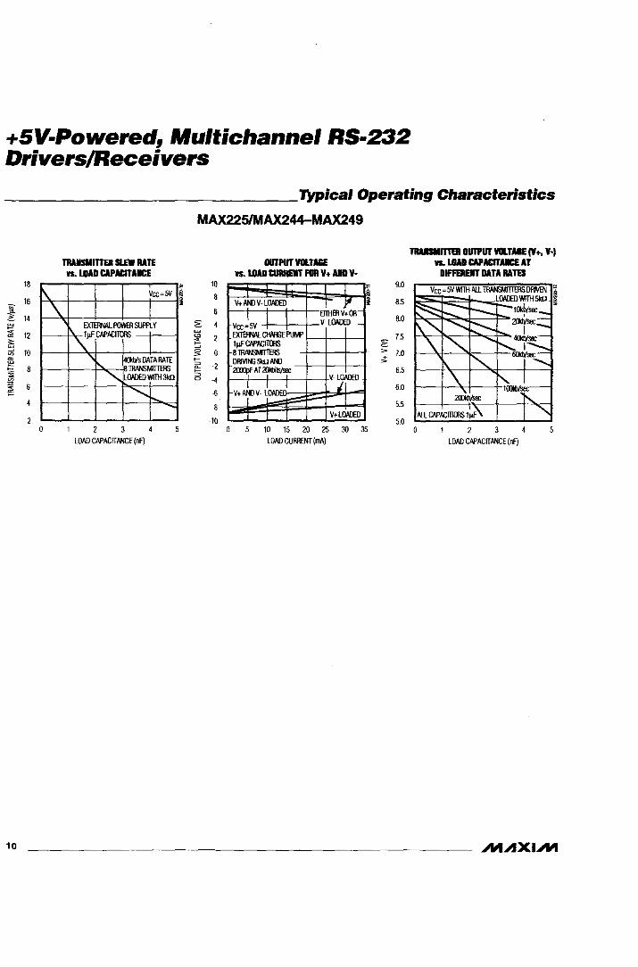
________________ l'ypical Operating Characteristics
MAX2251MAX244-MAX249
18
16 ]: C 14 ~ ~ 12
~ 10 f5 ~ 8 ~ ~
~ 6
10
\.
TllAllSlllTTEII Sl£W RATE IS. LOAD CAPACITAKE
• Vcc=5V ~
\. ~
EXTB!NAL POWER SUPPLY
~CAPACIlURS
"- :-... ~~OATARATE TRANSMIlTERS
" LONlElJ WITH 3I<n
" r-"
4
lOAD CAPACfTANCf (nF)
-
10
8
~ 4 ~
~ 2 §i 0 ~
K -2 to; o -.!
-6
~
-10
OIITPUT VIIlTAGE IS. LOAD CUlI1IElIT filii Y+ AID y.
I I ~ v+ ANJ V-LOAOOJ ~ERl(Jl- i Vcc~5V L I V-lOADED _
EXTB!NAL C!W«PlM' 1¢' CAPACIlURS 8 TRANSMITTERS 0RIVINi 5k11 ANJ 2(IXif AT ~ts/S8:
ViL V++V-~~ ~ I V+LOAOfO
10 15 20 25 30 3S
LOAD CURRENT (mA)
9.0
8.5
8.0
75 ~ ~ 7.0
6.5
6.0
5.5
5.0
TlIAISIIIITTEII OIITPUT VllLTAIE (y+, y., IS.. LOAD CAPACITAKE AT
DIfFEREJIT DATA RATES
LOAD CAPACfTANCE (nF)
At.AXIAt

+5V-Powered, Multichannel RS-232 Drivers!Receivers
+'JV
INPUT ).,-_...!!!rJV ____ I
;::OUT:::.;.:PU:.:..T_....:.-..i-!----mmmh-m-fmE ~ , , , , ,
, ,
tpoo.- _ --: i+-- tPHLT
Figure 1. Transmitter Propagation-Delay Timing
Rx lN ')o ..... J\J'l.Ar-4t-.. Vee- 2V
01 TEST CIRCUIT l~F
ENINPUT~ ov 11-· ~:-:~--- EN
--+i ;-- OUTPUT EN.ABLE TIME (tER)
:--- ------- +3.SV RECEIVER __ ~ OUTPUTS
bl ENABLE nMING
+O.BV
~ __ "':::V,--__ EN
ENINPUT~ -: ;.- OUTPUT OISABLE TIME (tDR)
VOH
RECEIVER OUTPUTS
.-; ------- VDH-OSV
VOL ___ -'.-: ------- VOL + OSV
cl DISABLE nMING
Vee - 2V
Figure 3. Receiver -Output Enable and Disable Timing
.M.AXI.M
, +3V _~ ___ h 50%
INPUT D'r 1----- 50%
, h~: hUV-;;-, __ 50% Vee OUTPUT -+-\ 50% 7--::::
: : '------t-: ..J __ ;- __ Gt>Il , , , , , ,
trHLR : \-- _~, :_, ttPlHSPLHfl tPHI.S-' ~
'EXCEPT FOR R2 ON THE MAX243 WHERE -3V IS UOfD.
Figure 2. Receiver Propagation-Delay Timing
SHDN _-'t3:e.V'----,1
OV
_: :.-- OUTPUT DISABLE TIME (tOT)
ji~. :--~ v- -------"1'----' !
al nMING DIAGRAM
10RO
bl TEST CIRCUIT
Figure 4. Transmitter-Output Disable Timing
11

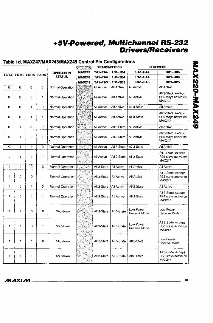
+SV-Powered, Multichannel RS-232 Drivers/Receivers Table 1a. MAX245 Control Pin Configurations
ENT ENR OPERATION STATUS TRANSMITTERS RECEIVERS
0 0 Normal Operation All Active All Active
0 1 Normal Operation All Active AlI3-State
1 0 Shutdown AlI3-State All Low-Power Receive Mode
1 1 Shutdown AII3-State AlI3-State
Table 1 b. MAX245 Control Pin Configurations
ENT ENR OPERATION TRANSMITTERS RECEIVERS
STATUS TA1-TA4 TB1-TB4 RA1-RA5 RB1-RB5
0 0 Normal Operation All Active All Active All Active All Active
0 1 Normal Operation All Active All Active RA l-RA4 3-State. RB l-RB4 3-State. RA5 Active RB5 Active
1 0 Shutdown AlI3-State AlI3-State All Low-Power All Low-Power Receive Mode Receive Mode
RA l-RA4 3-State. RB1-RB43-State. 1 1 Shutdown AlI3-State AlI3-State RA5 Low-Power RB5 Low-Power
Receive Mode Receive Mode
Table 1 c. MAX246 Control Pin Configurations
ENA ENB OPERATION TRANSMmERS RECEIVERS
STATUS TA1-TA4 TB1-TB4 RA1-RA5 RB1-RB5
0 0 Normal Operation All Active All Active All Active All Active
0 1 Normal Operation All Active AlI3-State All Active RB1-RB4 3-State. RBSActive
1 0 Shutdown AlI3-State All Active RA l-RA4 3-5tate.
All Active RA5 Active
RA1-RA4 3-5tate. RB1-RB43-51ale. 1 1 5hutdown A1I3-51ate AlI3-5tate RA5 Low-Power RA5 Low-Power
Receive Mode Receive Mode
12
+5V-Powered, Multichannel RS-232 Drivers!Receivers
Table 1d. MAX247IMAX2481MAX249 Control Pin ~nlnfif1I1rAtl'\nlii:
OPERATION STATUS
0 AlI3-State
0 0 Shutdown AlI3-State Al13-State Low-Power Low-Power Receive Mode Receive Mode
Low-Power All 3-State, except
0 Shutdown AlI3-State AlI3-State Receive Mode
RBS stays active on MAX247
0 Shutdown AlI3-State AlI3-State AlI3-State Low-Power Receive Mode
All 3-State, except Shutdown AlI3-State AlI3-State AlI3-State RBS stays active on
MAX247
13

+5V.Powered, Multichannel RS·232 Drivers!Receivers
______ Detailed Description The MAX220-MAX249 contain four sections: dual charge-pump DC-DC voltage converters, RS-232 drivers, RS-232 receivers, and receiver and transmitter enable control inputs.
Dual Charge-Pump Voltage Converter The MAX22~MAX249 have two internal charge-pumps that convert +5V to ±10V (unloaded) for RS-232 driver operation. The first converter uses capacitor C1 to double the +5V input to +1 OV on C3 at the V + output. The second converter uses capacitor C2 to invert + 1 OV to -10V on C4 at the V- output.
A small amount of power rnay be drawn from the + 10V (V+) and -10V (V-) outputs to power extemal Circuitry (see the Typical Operating Characteristics section), except on the MAX225 and MAX245-MAX247, where these pins are not available. V+ and V- are not regulated, so the output voltage drops with increasing load current. Do not load V+ and V- to a point that violates the minimum ±5V EIA/TIA-232E driver output voltage when sourcing current from V+ and V- to external circuitry.
When using the shutdown feature in the MAX222, MAX225, MAX230, MAX235, MAX236, MAX240, MAX241 , and MAX245-MAX249, avoid using V+ and Vto power external circuitry. When these parts are shut down, V- falls to OV, and V+ falls to +5V. For applications where a + 10V external supply is applied to the V+ pin (instead of using the internal charge pump to generate + 10V), the C1 capacitor must not be installed and the SHDN pin must be tied to Vee. This is because V+ is internally connected to Vee in shutdown mode.
RS-232 Drivers The typical driver output voltage swing is ±8V when loaded with a norninal 5kU RS-232 receiver and Vee = +5V. Output swing is guaranteed to meet the EIAffIA-232E and V.28 specification, which calls for ±5V minimum driver output levels under worst-case conditions. These include a minimum 3kn load, Vee = +4.5V, and maximum operating temperature. Unloaded driver output voltage ranges from (V+ -1.3V) to (V- +O.5V).
Input thresholds are both TIL and CMOS compatible. The inputs of unused drivers can be left unconnected since 400kO input pull-up resistors to Vee are built in (except for the MAX220). The pull-uP reSistors force the outputs of unused drivers low because all drivers invert. The intemal input pull-up reSistors typically source 121JA, except in shutdown mode where the pull-ups are disabled. Driver outputs turn off and enter a high-impedance state-where leakage current is typically microamperes (maximum 25iJA)-when in shutdown
14
mode, in three-state mode, or when device power is removed. Outputs can be driven to ±15V. The powersupply current typically drops to 81JA in shutdown mode. The MAX220 does not have pull-up resistors to force the outputs of the unused drivers low. Connect unused inputs to GND or Vee.
The MAX239 has a receiver three-state control line, and the MAX223, MAX225, MAX235, MAX236 , MAX240, and MAX241 have both a receiver three-state control line and a low-power shutdown control. Table 2 shows the effects of the shutdown control and receiver threestate control on the receiver outputs.
The receiver TIL/CMOS outputs are in a high-impedance, three-state mode whenever the three-state enable line is high (for the MAX225/MAX235/MAX236/MAX239-MAX241), and are also high-impedance whenever the shutdown control line is high.
When in low-power shutdown mode, the driver outputs are turned off and their leakage current is less than 1iJA \..,ith the driver output pulled to ground. The driver output ~eakage remains less than 1iJA, even if the transmitter output is backdriven between OV and (Vee + 6V). Below -0.5V, the transmitter is diode clamped to ground with 1kO series impedance. The transmitter is also zener clamped to approximately Vee + 6V, with a series impedance of 1 kO.
The driver output slew rate is limited to less than 30V /iJS as required by the EINTIA-232E and V.28 specifications. Typical slew rates are 24V/iJs unloaded and 10V/iJs loaded with 30 and 2500pF.
R5-232 Receivers EIAffIA-232E and V.28 specifications define a VOltage level greater than 3V as a logic 0, so all receivers invert. Input thresholds are set at 0.8V and 2.4V, so receivers respond to TIL level inputs as well as EIAffIA-232E and V.28 levels.
The receiver inputs withstand an input overvoltage up to ±25V and provide input terminating resistors with
Table 2. Three-State Control of Receivers PART SHDN SHDN EN EN(R) RECEIVERS
Low X High Impedance MAX223 - High Low - Active
High High High Impedance
MAX225 Low High Impedance
- - - High Active
MAX235 Low Low High Impedance MAX236 Low - - High Active MAX24D High X High Impedance
NI.AXINI

+5V.Powered, Multichannel RS·232 Drivers!Receivers
nominal 5k.Q values. The receivers implement Type 1 interpretation of the fault conditions of Y.28 and EINTIA-232E.
The receiver input hysteresis is typically 0.5Y with a guaranteed minimum of 0.2Y. This produces clear output transitions with slow-moving input signals. even with moderate amounts of noise and ringing. The receiver propagation delay is typically 600ns and is independent of input swing direction.
Low-Power Receive Mode The low-power receive-mode feature of the MAX223. MAX242. and MAX245-MAX249 puts the IC into shutdown mode but still allows it to receive information. This is important for applications where systems are periodically awakened to look for activity. Using low-power receive mode. the system can still receive a Signal that will activate it on command and prepare it for communication at faster data rates. This operation conserves system power.
Negative Threshold-NIAX243 The MAX243 is pin compatible with the MAX232A. differing only in that RS-232 cable fault protection is removed on one of the two receiver inputs. This means that control lines such as CTS and RTS can either be driven or left floating without interrupting communication. Different cables are not needed to interface with different pieces of equipment.
The input threshold of the receiver without cable fault protection is -0.8Y rather than + 1 .4Y. Its output goes positive only if the input is connected to a control line that is actively driven negative. If not driven. it defaults to the 0 or "OK to send" state. Normally. the MAX243's other receiver (+ 1.4Y threshold) is used for the data line (TO or RD). while the negative threshold receiver is connected to the control line (DTR. DTS. CTS. RTS. etc.).
Other members of the RS-232 family implement the optional cable fault protection as specified by EINTIA-232E specifications. This means a receiver output goes high whenever its input is driven negative. left floating. or shorted to ground. The high output tells the serial communications IC to stop sending data. To avoid this. the control lines must either be driven or connected with jumpers to an appropriate positive voltage level.
AII.AXIAII
Shutdo~22-MAJC242 On the MAX222. MAX235. MAX236. MAX240. and MAX241. all receivers are disabled during shutdown. On the MAX223 and MAX242. two receivers continue to operate in a reduced power mode when the chip is in shutdown. Under these conditions. the propagation delay increases to about 2.5/Js for a high-to-Iow input transition. When in shutdown, the receiver acts as a CMOS inverter with no hysteresis. The MAX223 and MAX242 also have a receiver output enable input (EN for the MAX242 and EN for the MAX223) that allows receiver output control independent of SHDN (SHDN for MAX241). With all other devices, SHDN (SHDN for MAX241) also disables the receiver outputs.
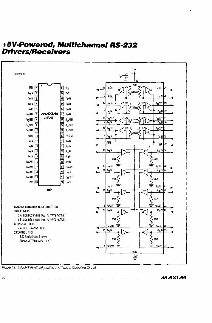
The MAX225 provides five transmitters and five receivers, while the MAX245 provides ten receivers and eight transmitters. Both devices have separate receiver and transmitter-enable controls. The charge pumps turn off and the devices shut down when a logic high is applied to the ENT input. In this state, the supply current drops to less than 25/JA anp the receivers continue to operate in a low-power receive mode. Driver outputs enter a high-impedance state (three-state mode). On the MAX225, all five receivers are controlled by the ENR input. On the MAX245, eight of the receiver outputs are controlled by the ENR input. while the remaining two receivers (RA5 and RB5) are always active. RA1-RA4 and RB1-RB4 are put in a three-state mode when ENR is a logic high.
Receiver and TransmiHer Ena"Ie Control Inputs
The MAX225 and MAX245-MAX249 feature transmitter and receiver enable controls.
The receivers have three modes of operation: full-speed receive (normal active), three-state (disabled), and lowpower receive (enabled receivers continue to function at lower data rates). The receiver enable inputs control the full-speed receive and three-state modes. The transmitters have two modes of operation: full-speed transmit (normal active) and three-state (disabled). The transmitter enable inputs also control the shutdown mode. The device enters shutdown mode when all transmitters are disabled. Enabled receivers function in the low-power receive mode when in shutdown.
15

+5V.Powered, Multichannel RS·232 Drivers/Receivers Tables 1a-1d define the control states. The MAX244 has no control pins and is not included in these tables.
The MAX246 has ten receivers and eight drivers with two control pins, each controlling one side of the device. A logic high at the A-side control input (ENA) causes the four A-side receivers and drivers to go into a three-state mode. Similarly, the B-side control input (ENB) causes the four B-side drivers and receivers to go into a three-state mode. As in the MAX24S, one Aside and one B-side receiver (RAS and RBS) remain active at all times. The entire device is put into shutdown mode when both the A and B sides are disabled (ENA = ENB = +SV).
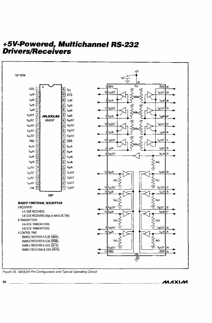
The MAX247 provides nine receivers and eight drivers with four control pins. The ENRA and ENRS receiver enable inputs each control four receiver outputs. The ENT A and ENTB transmitter enable inputs each control four drivers. The ninth receiver (RSS) is always active. The device enters shutdown mode with a logic high on both ENTA and ENTB.
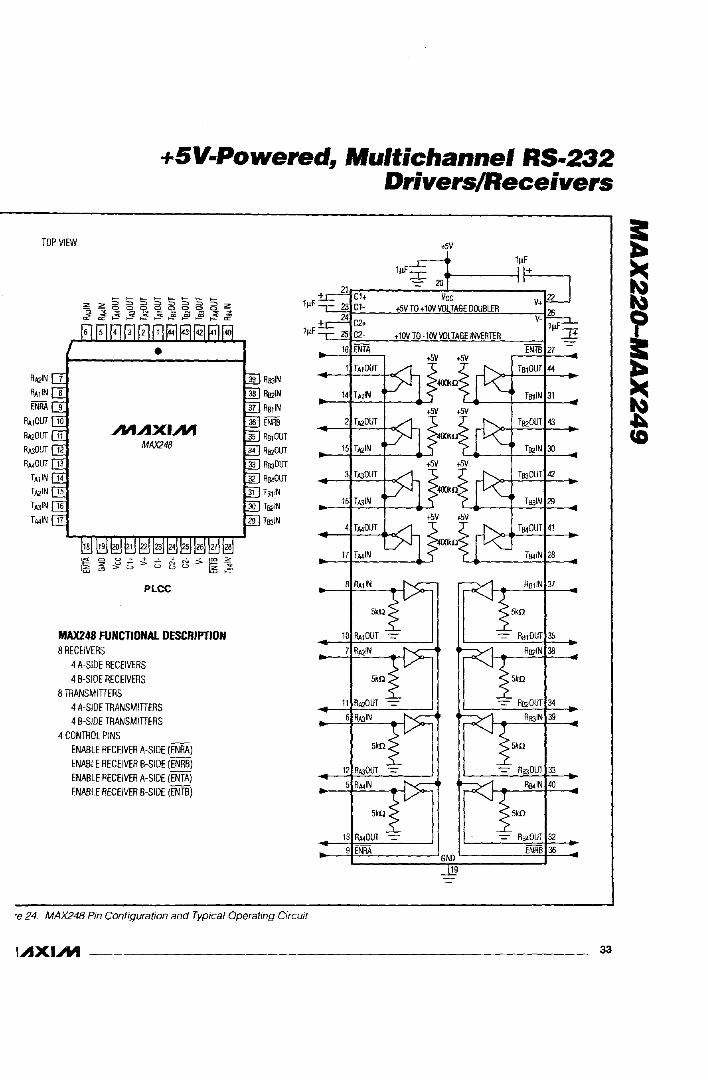
The MAX248 provides eight receivers and eight drivers with four control pins. The ENRA and ENRB receiver enable inputs each control four receiver outputs. The ENTA and ENTB transmitter enable inputs control four drivers each. This part does not have an always-active receiver. The device enters shutdown mode and transmitte~into a three-state mode with a logic high on both ENT A and ENTB.
16
The MAX249 provides ten receivers and six drivers with four control pins. The ENRA and ENRS receiver enable inputs each control five receiver outputs. The ENT A and ENTB transmitter enable inputs control three drivers each. There is no always-active receiver. The device enters shutdown mode and transmitters go into a three-state mode with a logic high on both ENTA and ENTB. In shutdown mode, active receivers operate in a low-power receive mode at data rates up to 20kbits/sec.
____ Applications Information Figures S through 2S show pin configurations and typical operating circuits. In applications that are sensitive to power-supply noise, VCC should be decoupled to ground with a capacitor of the same value as C1 and C2 connected as close as possible to the device.
+5V-Powered, Multichannel RS-232 Drivers!Receivers
iSV INPUT
TOP VIEW
Vee
V+ GND
C1- T10UT -1OV
C2+ R1~
R10UT
r nIH T10UT
"} TllJCMOS iSV
RS-232 T21H INPUTS 400kn OUTPUTS
R2'N R20UI 10 T2IN T20UT 7
DJP/sO 12 RloUT
"}~m TllJCMOS { OUTPUTS INPUTS
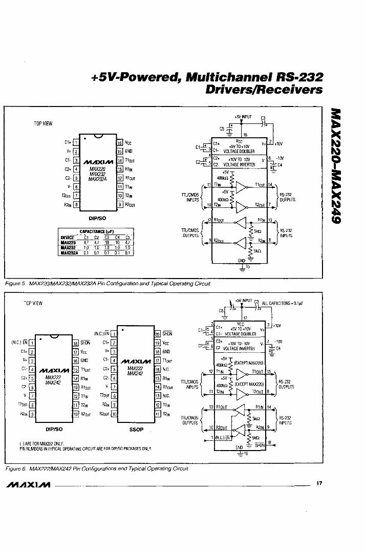
Figure 5. MAX22o;MAX232/MAX232A Pin Configuration and Typical Operating Circuit
TOP VIEW ~ +5V INPUT C3 ALL CAPACITORS, 0 1!'f
cs... +
SHDN C1
INC) EN 1 SHDN Cl+ Vee -1OV C2
C1+ Vee V+ GND
v+ GNC T10UI
T10UT N.C. 12 T10UT "} RlrN TI~MOS{ RS 232 R10UT R10UT INPUTS OUTPUTS
11 T20UT 8 nN T20m N.C.
R2,. T1,. 13 R11N 14 R21N R20UT T2'H
TIliCMOS { } RS-232 OUTPUTS 9 INPUTS
DIP/sO SSOP
I ) AREFOR MAX222 ONLY. PIN NUMBERS IN TYPICAL OPERATING CIRCUIT ARE FOR DIPiSO PACKAGES ONLY.
Figure 6. MAX222/MAX242 Pin Configurations and Typical Operating Circuit
.hIAXI.hI 17
E ~ ~ cp E ~ ,. U)

+SV.Powered, Multichannel RS·232 Drivers!Receivers
TOP VIEW
R,OUT
R:JIN
R:/IN
R,IN
T,OUT
so
MAX225 FUNCTIONAL DESCRIPTION 5 RECEIVERS 5 TRANSMITTERS 2 CONTROL PINS
1 RECEIVER ENABLE (ENR) 1 TRANSMITTER ENABLE (ENT)
Vee
Vee
ENT
T31N
T,IN
T51N
R,OUT
RsOUT
RsIN
R,IN
T30UT
T,OUT
PINS lENA, GND, Vee, T50UT) ARE INTERNALLY CONNECTED. CONNECT EITHER OR BOTH EXTERNALLY T50UT IS A SINGLE DRIVER
Figure 7, MAX225 Pm Configuration and Typical Operating Circuit
18
+5'1
3 T,IN
4 T21N
25 T31N
24 T,IN
23 T51N
26 00
11
12
18
17
16
15
R,IN 10
5kn
9
8
19
5kn
20
5kn
.M.AXI.M
+5V.Powered, Multichannel RS·232 Drivers!Receivers
TOP VIEW
T10ur
T20ur
Wide SOl SSOP
-R4 AND R51N MAX223 REMAIN ACTIVE IN SHUTDOWN
NOTE: PIN lABELS IN ( ) ARE FOR MAX241
T"N
RSour-
10¢
10¢
nUCMOS INPUTS
LOGIC OUTPUTS
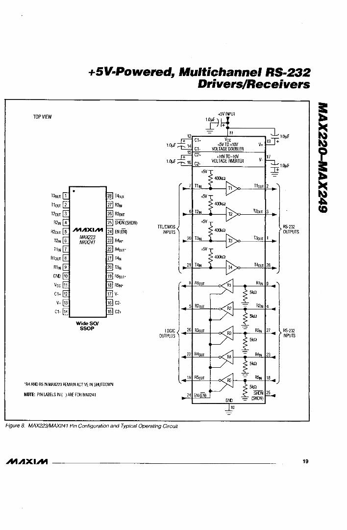
Figure 8. MAX223/MAX241 Pin Configuration and Typical Operating Circuit
.MAXIAt
20 131H
8 R10ur
;fN INPUT
~+ 11
Vee ;fNTO+1OV
VOLTAGE DOUBLER
+10VTO-IOV VOLTAGE INVERTER
It 10¢
T10ur 2
T20ur 3
RS-232 OUTPUTS
T30ur 1
T40ur 28
RIIN 9
5kn
R2IN 4
5kn
R3,N 27 R5-232 INPUTS
5kO
R4N 23
5kn
R~N 18
5kn SIilN 25
-= (SHON)
-
19
E ~ ~
~ ~
~ .. U»

+5V·Powered, Multichannel RS·232 Drivers!Receivers
TOP VIEW
130Ul
nOUl
n,. GMJ
Vee
C1+
OIPISO
HOUl
T5iN
N.C.
SHDN
1'5oUl
T4,.
131N
C2-
C2+
7gure 9. MAX230 Pin Configuration and Typical Operating Circuit
TOP VIEW
V+ V+
Vee C- Vee
GND GMJ
nOUl
RllN R2,. R1,.
R10UT R20Ul R1001
T1,. 11,. N.C. N_C.
DIP SO
PIN NUMBERS IN ( ) ARE FOR SO PACKAGE
"re 10. MAX231 Pin Configurations and Typical Operating Circuit
1.0!1F
1.0!1F
nuCMOS INPUTS
~C INPUTS
~C RtOUT
OUTPUTS
6 R20Ul
1.0!1F
':»="'-t2 .... \ RS-232 OUTPUTS
SHDN
+5V INPUT
-TlOUl
'l~ OUTPUTS T2001 4
'"}m RllN
INPUTS
R2JN 5
~.AXI.NI

+5V.Powered!l Multichannel RS·232 Drivers/Receivers
TOP VIEW
Tl,. RloUT
Rl,.
( ) AREFDR SO PACKAGE ONLY.
DIPISO
R20UT
R2,.
120UT
v-C2-
C2+
V+(Cl-)
C1-(Ch}
V- (C2+)
C2+(C2-)
2 TlIH
~{ INPUTS
12,. Rl0UT
=L R20UT , DO NOT MAKE 8 (13) C1+
CONNECTIONS TO {13 (14) Cl-
THESE PINS 12 (10)
INTERNAL -10 { V-POWER SUPPlY 17
INTERNAL +10V 14 (8) POWER SUPPlY
~jgure 11. MAX233/MAX233A Pin Configuration and Typical Operating Circuit
TOP VIEW
1.0~F
10~F
T2001 HOUl
12,. T4,. 4 n!H
Tl,. 13,.
GNO V-
Vee C2- 3 12,.
C2+ TTL/CMOS INPUTS
Cl-13 13'N
DIPISO
14 H,.
lure 12. MAX234 Pin Configuration and Typical Operating Circuit
-
GND GNO
-
TloUT 5
}~m OUTPUTS 120UT 18
· }~m R11N
OUTPUTS
R2,. 19
11 (12)
e2-C2-
nOUT
T20ur 3
130ur 16
T40ur 15
RS-232 OUTPUTS
21
E ~ ~
* • ~ • U)

+5V.Powered~ Multichannel RS·232 Drivers!Receivers
TOP VIEW
ffilCMOS INPUTS
R3'N
/l3oUT
nom T5'N
SHDN
EN
RZauT TSoUT
R41N
Tl,. R40UT
R10UT T41N
Rl" TI'N
R50UT
Vee R5~
DIP ffilCMOS OUTPUTS
11
'gure 13. MAX235 Pin Configuration and Typical Operating Circuit
TlOUT 3
120UT 4
T30Ul 2 R5-232 OUTPUTS
T40Ul 1
TSoUT 19
R5-232 INPUTS

TOP VIEW
T10UT
T2IH
GNO
+5V·Powered, Multichannel RS·232 Drivers/Receivers
DIPISO
R2"
R20Ul
SHDN
EN T41N
T3JN
R30uT
R31N
C2+
1.0pF
TTlJCMOS INPUTS
TIVCMOS OUTPUTS
,sVINPUT
1-L ...--------, 9
Vee ,sVTO+1DV
VOLTAGE DOUBLER
V-
7 nlN nOUl 2
18
GNO
8
RS-232 OUTPUTS
1\$-232 INPUTS
re 14. MAX236 Pin Configuration and Typical Operating Circuit
IAXI.hI 23
+SV.Powered, Multichannel RS.232 Drivers!Receivers
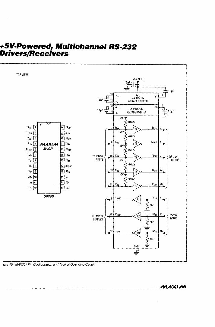
lure 15. MAX237 Pin Configuration and Typical Operating Circuit
~AXI.NI
TOP VIEW
DIP/SO
+5V.Powered, Multichannel RS·232 Drivers!Receivers
T30lJT
R3'N
R30lJT
T41N
T40lJT
13'N
T2'N
R40lJT
R4'N
v-C2-
C2+
1.il!lF
TTUCMOS INPUTS
TTUCMOS OUTPUTS
5 111N
18 12'N
19 T3'N
21 T41N
6 R10lJT
4 R20lJT
22 R30lJT
17 R40lJT
+5VINPUT
~cL..-_____ -, - 9
Vee +5VTO+1OV
V0l1AG£DOllBlER
HOlJT 2
T20lJT 1
T30lJT 24
T40lJT 20
RS-232 OUTPUTS
R5-232 INPUTS
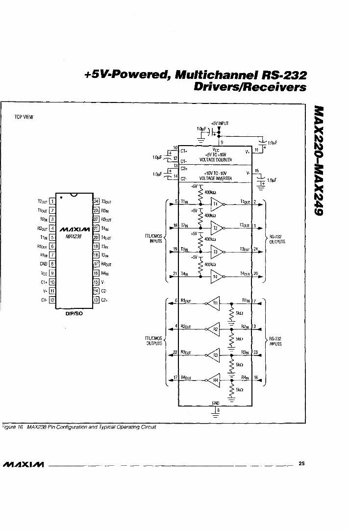
~igure 16. MAX238 Pin Configuration and Typical Operating Circuit
M.AXIAII 25

+5V-Powered, Multichannel RS-232 Drivers!Receivers
TOP VIEW 7.5'1 TO 132V
101lf
T11N
R11N T21N
R20llf nUCMOS INPUTS
R2w
T20llf
110llf
R31N
R30llf
T31N
N.C
EN
DlP/so nUCMOS
OUTPUTS
Figure 17. MAX239 Pin Configuration and TYPical Operating Circuit
26
+5V INPUT INPUT
:P+ - 4
Vee V+
+1OVTD -1OV VOlTAGE INVERTER
V- 8
110llf 19
T20lfT 20
T30llf 13
RS-232 OUTPUTS
RS-232 INPUTS

N.C.
Vee N.C N.C N.C.
TOP VIEW
+5V.Powered, Multichannel RS·232 Drivers!Receivers
AIIAXIAII MAX240
Plastic FP
N.C. SHlN EN
11:;;==TSour R4w R40ur T4,. 13'N R50ur RStN N.C
to¢'
nUCMOS INPUTS
nUCMOS OUTPUTS
15
14
42 EN
+5V INPUT
~ +.-------, 19
Vee +5VTO +1OV
VOLTAGE DOUBLER
V·
T10ur 7
R4'N 40
RS-232 OUTPUTS
R&-232 INPUTS
Figure 18. MAX240 Pin Configuration and Typical Operating Circuit
AI'I.AXI.AIi 27
+SV.Powered, Multichannel RS·232 Drivers!Receivers
TOP VIEW
C2+
C2-
T20llT
. DIP/SO
o
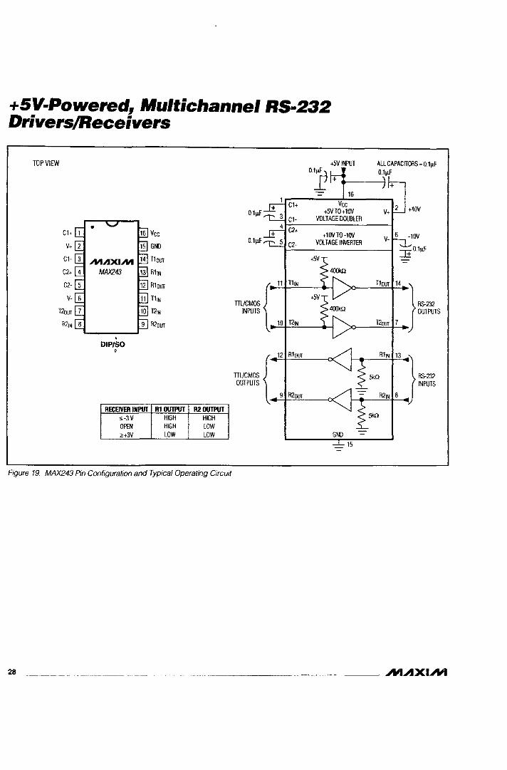
REtEIVER INPUT ~-3V
OPEN >+3V
R11N
R10llT
T11N
T21"
R1 OUTPUT HIGH HIGH LOW
R20UTPUT HIGH LOW LOW
Figure 19. MAX243 Pin Configuration and Typical Operating Circuit
28
+SV INPUT 0:r +
- 16 Vee
01!1f +SV TO +1OV VOLTAGE DOUBLER
0.1!1f
r T11"
TTUCMOS INPUTS
10 T21N
{" R10llT
TTl/CMOS OUTPUTS
9 R20IlT
GND 15
-
T10llT
.. } RS-232 OUTPUTS
T20llT 7
" } RS-232 INPUTS
R2IN 8
.hI..AXI.hI

+5V-Powered, Multichannel RS-232 Drivers/Receivers
TOP VIEW
•
~AXI~ MAX244
PLCC
MAX249 FUNCTIONAL DESCRIPTION 10 RECEIVERS
5 A-SIDE RECEIVER 58-SIDE RECEIVER
B TRANSMITTERS 4 A-SIDE TRANSMITTERS 4 8-SIDE TRANSMITTERS
NO CONTROL PINS
Ife 20. MAX244 Pin Configuration and Typical Operating Circuit
IAXI~
+5V
Vee t5V TO + lOY VOLTAGE DCXJBlER
GND 19
-TS1DUT 44
TIl1IN 30
T.,OUT 43
T.,IN 29
TB3DUT 42
TB3IN 28
TB40UT 41
TB4IN 27
RSllN 36
RB3IN 38
RB30UT 33
RB4IN 39
RB5IN 4D
29
+SV.Powered* Multichannel RS.232 Drivers!Receivers
TOP VIEW
ENR
T"IN
TA3IN
TMIN
R"OUT
ilM~Yf
R"OUT
RA1 0UT
R"IN
RA3IN
RAAIN
R"IN
TAl OUT
T"oUT
TA30UT
TAAoUT
GNO
DIP
MAX245 FUNCTIONAL DESCRIPTION 10 RECEIVERS
5 A-SIDE RECEIVERS (RA5 ALWAYS ACTIVE) 5 B-SIDE RECEIVERS (RB5 ALWAYS ACTIVE)
B TAANSMITITERS 4 A-SIDE TAANSMITIERS
2 CONTROL PINS 1 RECEIVER ENABLE (ENR) 1 TAANSMITIER ENABLE (ENT)
Vee
ENT
TB1IN
T62IN
TrolN
T"IN
~Yf
RroOUT
RS1 0UT
RSlIN
R62IN
RrolN
R"IN
RsslN
TSloUT
T620UT
TrooUT
TB40UT
Figure 21. MAX245 Pin Configuration and Typical Operating Circuit
30
¥5V
l~F :::r:: - 40
16 TAl OUT
2 TA1IN
17 T"oUT
3 T"IN
18 TA30UT 4 TA3IN
19 TMOUT
S TMIN
1 ENR
11 RAllN
10 RA10UT
12 R"IN
Sku
9 R"OUT
13 RA3IN
GNO 20
TB10UT 24
TB1IN 38
T62DlIT 23
T62IN 37
TroOUT 22
TrolN 36
T"OUT 21
T"IN 35
ENT 39
RSllN 29
R"OUT 30
R"IN 28
R"OUT 31
RrolN 27
.MAXI.M

+SV-Powered, Multichannel RS·232 Drivers/Receivers
TOP VIEW ;5V
40
ENA Vee ;5V Vee ;5V
TA,IN ENB 16 TA'OUT TB10UT 24
T"IN TB1IN 2 TA,IN TB1IN 38
T",IN
TI!3IN 17 T"oUT T",OUT 23
RASOUT TS4IN 3 T"IN T",IN 37
RssOUT
RA30UT RS40UT 18 TA30UT TI!30UT 22
RI!30UT 4 TA3IN
RA'OUT TI!3IN 36
RB'OUT 19 TAAOUT TS40UT 21
R"IN RB,IN TB4IN 35 5 TAAIN
RA3IN R",IN 1 ENA ENB 39
RMJN RI!3i>1 11 R..,IN RBlIN 29
RASIN RB4IN
TA'OUT RsslN
T"OUT TB10UT R..,OUT RB10UT 30 10
TA30UT T",OUT 12 R"IN R",IN 28
TA40UT TI!30UT
GND TB40UT
DIP 9 R"OUT R",OUT 31
13 RA3IN RI!3IN 27
MAX246 FUNCTIONAL DESCRIPTION 10 RECEIVERS
B RA3DUT R"OUT 32 5 ~-SIOE RECEIVERS (RA5 ALWAYS ~CTIVE)
14 RAAIN RS4IN 26 58-SIDE RECEIVERS IR85 ALWAYS AcnVE)
8 TRANSMITTERS 4 A-SIDE TRANSMITTERS 4 8-SIDE TRANSMITTERS 7 RAAOUT RMOUT 33
2 CONTROL PINS 15 RASIN RsslN 25 ENABLE A-SIDE lENA) ENABLE 8-SIDE IEN8)
34
-
Figure 22. MAX246 Pin Configuration and Typical Operating Circuit
.MAX.AII 31
E ~ ~ E ~ 6 CD
+5V.Powered, Multichannel RS·232 Drivers!Receivers
+5V
TOP VIEW
- 4lJ
1 ENTA Vee Vee +5V +5V
16 T.,OUT TAl IN ENTB
T"IN TBlIN 2 TAllN
T"IN TMIN TB3IN
17 T"OUT
RBsOUT T84IN 3 T"IN R840UT
R",OUT RB30UT 18 T",OUT
R"OUT R"oUT 4 T",IN R.,OUT RBlOUT
ENRA ENRB 19 TMOUT
RAllN RBlIN 5 TMIN
R"IN R"IN 6 RasOUT
R",IN RB3IN
RMIN R84IN
TA,OUT RaslN
T"OUT TBlOUT 12 RA,IN
T",OUT T",OUT
TMOUT TB3DUT
GNO 10 RA10UT
13 R"IN DIP
MAX247 FUNCTIONAL DESCRIPTION 9 RECEIVERS 9 R"OUT
4 A~SIDE RECEIVERS 14 R",IN 5 B~SIDE RECEIVERS (RB5 ALWAYS ACTIVE)
8 TRANSMITTERS 4 A~SIDE TRANSMITTERS
4 B~SIDE TRANSMITTERS 8 R",OUT
4 CONTROL PINS 15 RMIN
ENABLE RECEIVER A~SIOE (ENRA)
ENABLE RECEIVER B-SIDE (ENRB)
ENABLE RECEIVER A~SIOE (ENTA) 7 RMOUT
ENABLE RECEIVERr B~SIDE (ENTB) 11 ENRA
GNO 20
-
Figure 23. MAX247 Pin Configuration and Typical Operating Circuit
32
ENTB 39
RaslN 25
RBlIN 29
RB10UT 31
R"IN 28
R"OUT 32
RB3IN 27
RB30UT 33
RB4IN 26
R840UT 34
ENRB 30
AlI.AXI.hI
+SV.Powered, Multichannel RS·232 Drivers/Receivers
TOP VIEW
•
..NIAXI..NI MAX248
PLCC
MAX248 FUNCTIONAL DESCRIPTION 8 RECEIVERS
4 A-SIDE RECEIVERS 4 B-SIDE RECEIVERS
8 TRANSM ITTERS 4 A-SIDE TRANSMITTERS 4 B-SIDE TRANSMITTERS
4 CONTROL PINS ENABLE RECEIVER A-SIDE (ENRA) ENABLE RECEIVER B-SIDE (ENRB) ENABLE RECEIVER A-SIDE (ENTA) ENABLE RECEIVER B-SlDE (ENTS)
RB3IN
R82IN
RSlIN
ENRB
R"OUT
RWlUT RB3DUT
R"OUT
T82IN
TB3IN
-e 24_ MAX248 Pin Configuration and Typical Operating Circuit
I.AXI.M
18 ENTA
8 RAllN
+f;V
1j1f 1j1f...,
20
Vee +fiV TO +lOVVDLTAGE DOUBLER
+lOV TO-1OV VOLTAGE INVERTER
ENTB 27
TB10UT 44
T"IN 31
T82DUT 43
T82IN 30
TB3DUT 42
TB3IN 29
T"OUT 41
T"IN 28
R81IN 37
19
33
E ~ , E ~ 6 CO

+SV·Powered, Multichannel RS·232 Drivers!Receivers
TOP VIEW
R,..,OUT
RA20UT 11 .JMAXI.JM MAX249
R"OUT
RMOUT
PLCC
MAX249 FUNCTIONAL DESCRIPTION 10 RECEIVERS
5 A-SIDE RECEIVERS 5 B-SIDE RECEIVERS
6 TRANSMITIERS 3 A-SIDE TRANSMITIERS 3 8-SIDE TRANSMITIERS
4 CONTROL PINS ENABLE RECEIVER A-SIDE {ENRAl ENABLE RECEIVER B-SIDE {ENRBl ENABLE RECEIVER A-SIDE {ENTAl ENABLE RECEIVER B-SIDE (ENTS)
Figure 25. MAX249 Pin Configuration and Typical Operating Circuit
34
Vee +5V TO +1OV VOLTAGE OOUBLfR
+1OV TO -1OV VOLTAGE INVERTER
+9/ +5V 1 TA10UT
15 TA1IN
2 T"OUT
16 T"IN
3 T"OUT
17 TA3IN
8 RA1IN
10 ""OUT
9 ENRA GNO
19
-ENTB 27
T.,OUT 44
Tm lN 30
TB20UT 43
TB2IN 29
TB30UT 42
TB3IN 28
R"IN 37
Rs4IN 40
RB40UT 32
RsslN 41
RssOUT 31
.hIAXI.hI

+5V.Powered, Multichannel RS·232 Drivers/Receivers
_________________ Ordering Information (continuedJ
PART TEMP RANGE PIN-PACKAGE PART TEMP RANGE PIN-PACKAGE
MAX222CPN O"C to + 70"C 18 Plastic DIP MAX232AC/D O°C to + 70"C Dice"
MAX222CWN DoC to + 70"C 18 Wide SO MAX232AEPE -40°C to +85°C 16 Plastic DIP
MAX222C/D DoC to +70°C Dice" MAX232AESE -40"C to +85°C 16 Narrow SO
MAX222EPN -40°C to +85°C 18 Plastic DIP MAX232AEWE -40°C to +85°C 16 Wide SO
MAX222EWN -40°C to +85°C 18 Wide SO MAX232AEJE -40°C to +85°C 16CERDIP
MAX222EJN -40°C to +85°C 18 CERDIP MAX232AMJE -55°C to +125°C 16 CERDIP
MAX222MJN -55°C to + 125°C 18CERDIP MAX232AMLP -55°C to + 125°C 20LCC
MAX223CAI O"C to + 70°C 28SS0P MAX233CPP O"C to + 70DC 20 Plastic DIP
MAX223CWI O"C to + 70°C 28 Wide SO MAX233EPP -40°C to +85°C 20 Plastic DIP
MAX223C/D O"C to + 70°C Dice" MAX233ACPP OOC to + 70"C 20 Plastic DIP
MAX223EAI -40°C to +85°C 28SS0P MAX233ACWP O°C to +70°C 20 Wide SO
MAX223EWI -40°C to +85°C 28 Wide SO MAX233AEPP _40DC to +85°C 20 Plastic DIP
MAX225CWI DOC to +7DoC 28 Wide SO MAX233AEWP -40°C to +85°C 20 Wide SO
MAX225EWI -40°C to +85°C 28 Wide SO MAX234CPE O"C to + 70°C 16 Plastic DIP
MAX23OCPP" DoC to +70°C 20 Plastic DIP MAX234CWE DoC to +70DC 16 Wide SO
MAX230CWfll O"C to + 7D"C 20 Wide SO MAX234C/D O°C to + 70"C Dice"
MAX23DC/D DoC to +7DoC Dice' MAX234EPE _40DC to +85DC 16 Plastic DIP
MAX23DEPP -40°C to +85°C 20 Plastic DIP MAX234EWE -40°C to +85°C 16 Wide SO
MAX23DEWP -40°C to +85°C 20 Wide SO MAX234EJE -40DC to +85DC 16 CERDIP
MAX230EJP -40°C to +85°C 20CERDIP MAX234MJE -55°C 10 + 125DC 16CERDIP
MAX230MJP -55°C to + 125°C 20CEROIP MAX235CPG DOC to +70°C 24 Wide Plastic DIP
MAX231CPD DoC to +70°C 14 Plastic DIP MAX235EPG -40°C to +85°C 24 Wide Plastic DIP
MAX231CWE DoC to +70°C 16 Wide SO MAX235EDG -40"C to +85°C 24 Ceramic S8
MAX231CJD DoC to +70°C 14 CERDIP MAX235MDG -55°C to + 125°C 24 Ceramic S8
MAX231C/D O"C to + 70DC Dice" MAX236CNG DoC to +70°C 24 Narrow Plastic DIP
MAX231EPD -40°C to +85°C 14 Plastic DIP MAX236CWG O°C to +70°C 24 Wide SO
MAX231 EWE -40°C to +85DC 16 Wide SO MAX236C/D O°C to +70°C Dice"
MAX231EJD -40°C to +85DC 14 CERDIP MAX236ENG -40°C to +B5°C 24 Narrow Plastic DIP
MAX231MJD -55°C to + 125°C 14 CERDIP MAX236EWG _40DC to +85DC 24 Wide SO
MAX232CPE DoC to +70°C 16 Plastic DIP MAX236ERG -40"C to +85°C 24 Narrow CERDIP
MAX232CSE O°C to +70°C 16 Narrow SO MAX236MRG -55DC to + 125°C 24 Narrow CERDIP
MAX232CWE DoC to +70°C 16 Wide SO MAX237CNG DoC to +70DC 24 Narrow Plastic DIP
MAX232C/D O"C to + 70"C Dice" MAX237CWG DoC to +70DC 24 Wide SO
MAX232EPE -40°C to +85°C 16 Plastic DIP MAX237C/D DoC to +70°C Dice"
MAX232ESE -40°C to +85°C 16 Narrow SO MAX237ENG -40°C to +85°C 24 Narrow Plastic DIP
MAX232EWE -40°C to +85°C 16 Wide SO MAX237EWG -40°C to +85°C 24 Wide SO
MAX232EJE -40°C to +85°C 16 CERDIP MAX237ERG -40°C to +8SDC 24 Narrow CERDIP
MAX232MJE -55°C to + 125°C 16 CERDIP MAX237MRG -SSDC to + 12SoC 24 Narrow CERDIP
MAX232MLP -55°C to + 125°C 20LCC MAX238CNG O°C to +70"C 24 Narrow Plastic DIP
MAX232ACPE O°C to + 70"C 16 Plastic DIP MAX238CWG O°C to + 70"C 24 Wide SO
MAX232ACSE DoC to +70°C 16 Narrow SO MAX238C/D ODC to +70°C Dice'
MAX232ACWE O°C to +70°C 16Wide SO MAX238ENG -40°C to +BSoC 24 Narrow Plastic DIP
• Contact factory for dice specifications .
.M~XI.M 35

+SV-Powered, Multichannel RS-232 Drivers/Receivers
_________________ Ordering Information (continued]
PART TEMP RANGE PIN-PACKAGE
MAX238EWG -40°C to +85°C 24 Wide SO
MAX238ERG -40°C to +85°C 24 Narrow CERDIP
MAX238MRG -55°C to +125°C 24 Narrow CERDIP
MAX239CNG O°C to +70°C 24 Narrow Plastic DIP
MAX239CWG O°C to +70°C 24 Wide SO
MAX239C/D OOC to +70OC Dice-
MAX239ENG -40°C to +85°C 24 Narrow Plastic DIP
MAX239EWG -40°C to +85°C 24 Wide SO
MAX239ERG -40°C to +85°C 24 Narrow CERDIP
MAX239MRG -55°C to +125°C 24 Narrow CERDIP
MAX240CMH O°C to +70°C 44 Plastic FP
MAX24DC/D DOC to +7DoC Dice*
MAX241CAI DoC to +70°C 28SS0P
MAX241CWI DoC to +70°C 28 Wide SO
MAX241C/D DoC to +70°C Dice* .
MAX241EAI -40°C to +85°C 28 SSOI'
MAX241EWI -40°C to +85°C 28 Wide SO
MAX242CAP DoC to +70°C 20SS0P
MAX242CPN DoC to +70°C 18 Plastic DIP
MAX242CWN DoC to +70°C 18WideSO
MAX242C/D DoC to +70°C Dice'"
MAX242EPN -40°C to +85°C 18 Plastic DIP
MAX242EWN -40°C to +85°C 18Wide SO
MAX242EJN -40°C to +85°C 18CERDIP
MAX242MJN -55°C to + 125°C 18 CERDIP
PART TEMP RANGE PIN-PACKAGE MAX243CPE DOC to +70°C 16 Plastic DIP
MAX243CSE DoC to +70°C 16 Narrow SO
MAX243CWE DoC to +70OC 16WideSO
MAX243C/D DoC to +70°C Dice*
MAX243EPE -40°C to +85°C 16 Plastic DIP
MAX243ESE -40"C to +85°C 16 Narrow SO
MAX243EWE -4DoC to +85°C 16Wide SO
MAX243EJE -40°C to +85°C 16 CERDIP
MAX243MJE -55°C to + 125°C 16 CERDIP
MAX244COH O°C to +70°C 44PLCC
MAX244C/D DOC to +7DoC Dice'" MAX244EOH -40°C to +85°C 44PLCC
MAX245CPL O°C to +70°C 40 Plastic DIP
MAX245C/D DoC to +70°C Dice"
MAX245EPL -40°C to +85°C 40 Plastic DIP
MAX246CPL DOC to +70°C 40 Plastic DIP
MAX246C/D DoC to +70°C Dice*
MAX246EPL -40°C to +85°C 40 Plastic DIP
MAX247CPL DoC to +70°C 40 Plastic DIP
MAX247C/D DoC to +70°C Dice*
MAX247EPL -40°C to +85°C 40 Plastic DIP
MAX248COH DoC to +70°C 44 PLCC
MAX248C/D DoC to +70°C Dice*
MAX248EOH -40°C to +85°C 44 PLCC
MAX249COH DoC to +70°C 44 PLCC
MAX249EOH -40°C to +85°C 44 PLCC
• Contact factory for dIce speCIfIcations.
______ Paclcage Information For the latest package outline information, go to www.maxim-ic.com/packaaes.
Maxim cannot assume responsibility far use of any Circuitry other than Circuitry entirety embodied in a Maxim product. No circuit patent licenses are implied. Maxim reserves the right to change the circuitry and specifications without notice at any time
36 _______ Maxim Integrated Products, 120 San Gabriel Drive, Sunnpale, CA 94086 (408} 737·7600
© 2003 Maxim Integrated Products Printed USA .NUIXIAII is a registered trademark of Maxim Integrated Products.
November 1997
Features
• 25A and 28A, SOV and 100V
• rDS(ON) = O.077n and 0.100n
IRF540, IRF541, IRF542, IRF543, RF1S540, RF1S540SM
25A and 28A, 80V and 100V, 0.077 and 0.100 Ohm, N-Channel Power MOSFETs
Description
• Single Pulse Avalanche Energy Rated
These are N-ChanneJ enhancement mode silicon gate power field effect transistors. They are advanced power MOSFETs designed, tested, and guaranteed to withstand a specified level of energy in the breakdown avalanche mode of operation. All of these power MOSFETs are designed for applications such as switching regulators, switching convertors, motor drivers, relay drivers, and drivers for high power bipolar switching transistors requiring high speed and low gate drive power. These types can be operated directly from integrated circuits.
• Nanosecond Switching Speeds
• Linear Transfer Characteristics
• High Input Impedance
• Related Literature • TB334 "Guidelines for Soldering Surface Mount
Components to PC Boards" Formerly developmental type TA17421.
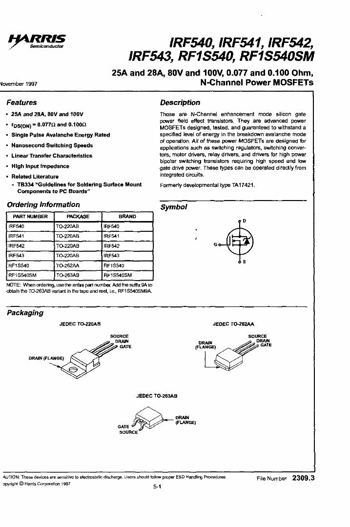
Ordering Information Symbol PART NUMBER PACKAGE BRAND
IRF540 T0-220AB IRF540
IRF541 T0-220AB IRF541
IRF542 T0-220AB IRF542
IRF543 T0-220AB IRF543
RF1S540 T0-262AA RF1S540
RF1S540SM T0-263AB RF1S540SM
NOTE: When ordering, use the entire part number.1Idd the suffix 9A to obtain the T0-263AB variant in the tape and reel, i.e., RF1 S540SM9A
Packaging
JEDEC TO-220AB
SOURCE DRAIN
GATE
JEDEC T0-263AB
~DRAlN (FLANGE)
GATE SOURCE
G
s
JEDEC T0-262AA
SOURCE DRAIN
/'-4~~"" GATE
AUTION: These devices are sensitive to electrostatic discharge. Users should follow proper ESO Handling Procedures. File Number 2309.3 opyright © Harris Corporation 1997
5-1
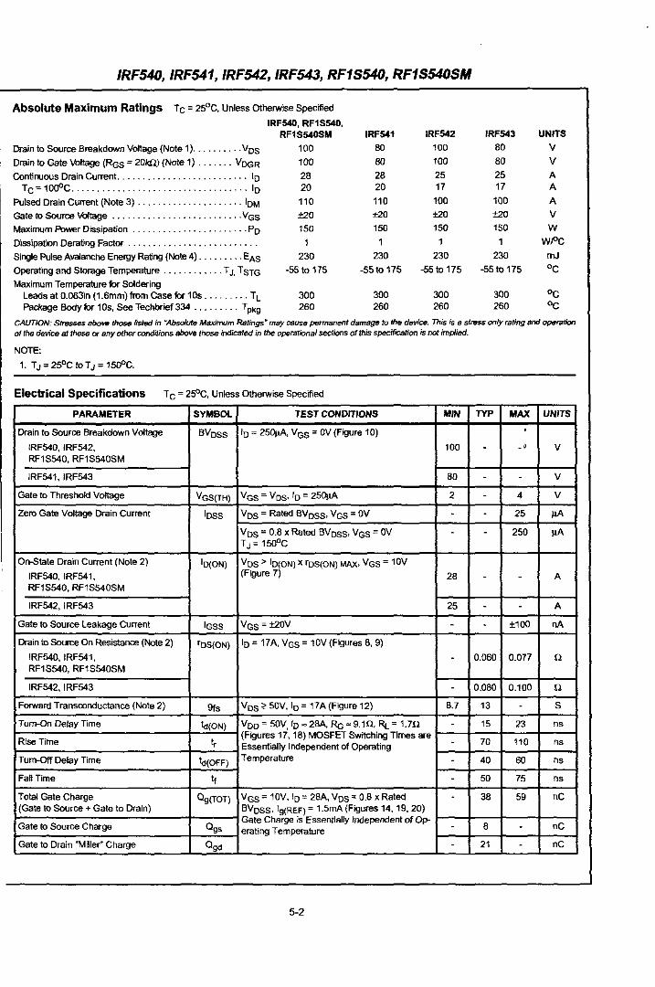
IRF540, IRF541, IRF542, IRF543, RF1S540, RF1S540SM
Absolute Maximum Ratings T c = 25°C. Unless Otherwise Specified
IRF540. RF1S540. RF1S54DSM IRF541 IRF542 IRF543 UNITS
Drain to Source Breakdown Voltage (Note 1) .......... VOS 100 SO 100 80 V
Drain to Gate Voltage (RGS = 20k!2) (Note 1) ....... VOGR 100 BO 100 80 V
Continuous Drain Current. ......................... 10 28 28 25 25 A
T C = 1000C ................................... 10 20 20 17 17 A
Pulsed Drain Current (Note 3) ..................... 10M 110 110 100 100 A
Gate to Source Voltage .......................... V GS ±20 ±20 ±20 ±20 V
Maximum Power Dissipation ....................... Po 150 150 150 150 W
Dissipation Derating Factor .......................... 1 1 1 1 Wf'C
Siegle Pulse Avalanche Energy Rating (Note 4) ......... EAS 230 230 230 230 mJ
Operating and Storage Temperature ............ T J. T STG -55 to 175 -55 to 175 -55 to 175 -55 to 175 °c
Maximum Temperature b- Soldering Leads at 0.063in (1.6mm) from Case for lOs ......... T L 300 300 300 300 °c
Package Body for lOs. See Techbrief 334 ......... T pkg 260 260 260 260 °c
CAUTION: Stresses abo"" those listed in ~AbsoIut" Maximum Ratings- may cause permanent damage to the device. This;s 8 stress only rating and optH'Blion of the device at these or any other conditions above those indicated in the operational sections of this specffication is not implied.
NOTE:
1. TJ = 25°C to TJ = 15O"C.
Electrical Specifications T C = 2SOC. Unless Otherwise Specified
PARAMETER SYMBOL TEST CONDITIONS MIN TYP MAX UNITS
Drain to Source Breakdown Voltage BVOSS 10 = 250JiA, VGS = OV (Figure 10) . IRF540. IRF542, 100 - -, V RFl S540. RF1 S540SM
IRF541,IRF543 80 - - V
Gate to Threshold Voltage VGS(TH) VGS = VOS' 10 = 25O!IA 2 - 4 V
Zero Gate Voltage Drain Current loss VOS = Rated BVOSS, VGS = OV - - 25 IlA
VOS = 0.8 x Rated BVOSS, VGS = OV - - 250 IlA TJ=15O"C
OM3tate Drain Current (Note 2) ID(ON) VOS> 10(ON) x rOS(ON) MAX. VGS = 10V
IRF540, IRF541, (Figure 7) 28 - - A RF1S540, RF1S540SM
IRF542, IRF543 25 - - A
Gate to Source Leakage Current IGSS VGS =±20V - - ±100 nA
Drain to Source On Resistance (Note 2) rOS(ON) 10 = 17A. VGS = 10V (Figures 8, 9)
IRF540, IRF541. - 0.060 0.077 0 RF1S540. RF1S540SM
IRF542. IRF543 - 0.080 0.100 0
Forward Transconductance (Note 2) 9ts VOs " 50V. 10 = 17A (Figure 12) 8.7 13 - S
Tum-On Delay Time t.l{ON) Voo = 50V.lo ~28A. % ~ 9.10. RL = 1.70 - 15 23 ns
Rise Time tr (Figures 17. 18) MOSFET Switching Times are - 70 110 ns Essentially Independent of Operating
Tum-Off Delay Time !"(OFF) Temperature - 40 60 ns
Fall Time tf - 50 75 ns
T olal Gate Charge Og(TOT) VGS = 10V. 10 = 28A. VOS = 0.8 x Rated - 38 59 nC (Gate to Source + Gate to Drain) BVOSS. Ig{REF) = 1.5mA (Figures 14. 19.20)
Gate to Source Charge Qgs Gate Charge is Essentially Independent of Op- - 8 nC erating Temperature -
Gate to Drain "Miller" Charge Qgd - 21 - nC
5-2
IRF540, IRF541, IRF542, IRF543, RF1S540, RF1S540SM
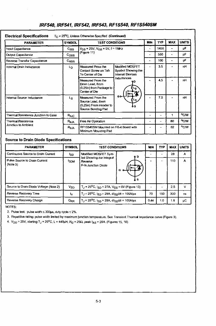
Electrical Specifications T c = 25"C, Unless Otherwise Specified (Continued)
PARAMETER SYMBOL TEST CONDITIONS MIN TYP MAX UNITS
Input Capacitance CISS VOS = 25V, VGS = OV, f -1MHz - 1450 - pF
Output Capacitance COSS (Figure 11) - 550 - pF
Reverse Transfer Capacitance CRSS - 100 - pF
Internal Drain Inductance Lo Measured From the Modified MOSFET - 3.5 - nH Contact Screw on Tab Symbol Showing the To Center of Die Internal Devices
Measured From the Inductances
4.5 nH 'tD - -Drain Lead, 6mm
.~ (0.25in) from Package to Center of Die
Internal Source Inductance Ls Measured From the - 7.5 - nH Source Lead, 6mm (0.25in) From Header to h Source Bonding Pad
Thermal Resistance Junction to Case ReJc - - 1 °CIW
Thermal Resistance RaJA Free Air Operation - - 80 0eJW Junction to Ambient
ReJA RF1S540SM Mounted on FR-4 Board with 62 °CIW - -Minimum Mounting Pad
Source to Drain Diode Specifications
PARAMETER SYMBOL TEST CONDITIONS MIN TYP MAX UNITS
Continuous Source to Drain Current ISO Modified MOSFET Sym-
~ - - 28 A
Pulse Source to Drain Current boI Showing the Integral
ISOM Reverse - - 110 A (Note 3) P-N Junction Diode
G~~ S
Source to Drain Diode Voltage (Note 2) VSO T J = 25°C. Iso = 27 A, VGS = OV (Figure 13) - - 2.5 V
Reverse Recovery Time Irr T J = 25°C, ISO = 28A, dlSo'dt = 100AlJIs 70 150 300 ns
Reverse Recovery Charge ORR TJ = 25°C, ISO = 28A, dlSo'dt = 100NJIs 0.44 1.0 1.9 JIC
NOTES:
2. Pulse test pulse width <; 300~, duty cycle S 2%.
3. Repetttive rating: pulse width limited by maximum junction temperature. See Transient Therrnallmpedance curve (Figure 3).
4. Voo = 25V, starting TJ = 25°C, L = 44O!!H, % = 250, peak lAS = 28A. (Figures 15,16).
5-3

IRF540, IRF541, IRF542, IRF543, RF1S540, RF1S540SM
Typical Performance Curves Unless Otherwise Specified
IX W :::; "-is ::J :E z g
~ 0; !!2 Q IX W
~ ...
1.2
1.0
~ 0.8
0.6
0.4
0.2
o o 25
"-~ " ~ .......
~ ~
50 75 100 125 150 175
Te. eASE TEMPERATURE ("C)
FIGURE 1. NORMALIZED PONER DISSIPATION vs CASE TEMPERATURE
-------
~0.01"-0.01 ...... 1-"
10""
30
g24
... z lii! 18 IX ::>
'" 3l 12 ~ c .E
6
0 25 50 75 100 125 150
T c. CASE TEMPERATURE ("C)
FIGURE 2. MAXIMUM CONTINUOUS DRAIN CURRENT vs CASE TEMPERATURE
," RECTANGUlAR PULSE DURATION (5)
FIGURE 3. MAXIMUM TRANSIENT THERMAL IMPEDANCE
IRF54{j~ '. RF1~s40: ~~ Te = 25°C
IRF542, 3 10us :±= 100 50
IlOjJS pULSE TEST
:r..
175
g IRF540. 1. RF·"~540. ~M
100jJS - g ry-:::. VGS= lOY VGS =: 7V ..
IRF542, 3 .. , ...
z w IX IX
... 40 z W IX IX
VGS= BV
. i I~ ~ .. 1ms ::J
'" 10 ::J 30
'" VGS= 6V-
OPERATION IN THIS 10ms :E AREA MAY BE ro.. ., LIMITED BY restON} ~~ TJ = MAX RATED
IRF541.3 DC -!;
SINGLE PULSE ...... I I I-II -...-~~
, "
z :;;: IX C
.9
1 1 10 100
z < IX 20 Q
.9 10
0 0
VGS= 5V
VGS= 4V
12 36 46 24 60 Vas. DRAIN TO SOURCE VOLTAGE M Vas. DRAIN TO SOURCE VOLTAGE M
FIGURE 4. FORWARD BIAS SAFE OPERATING AREA FIGURE 5. OUTPUT CHARACTERISTICS
5-4
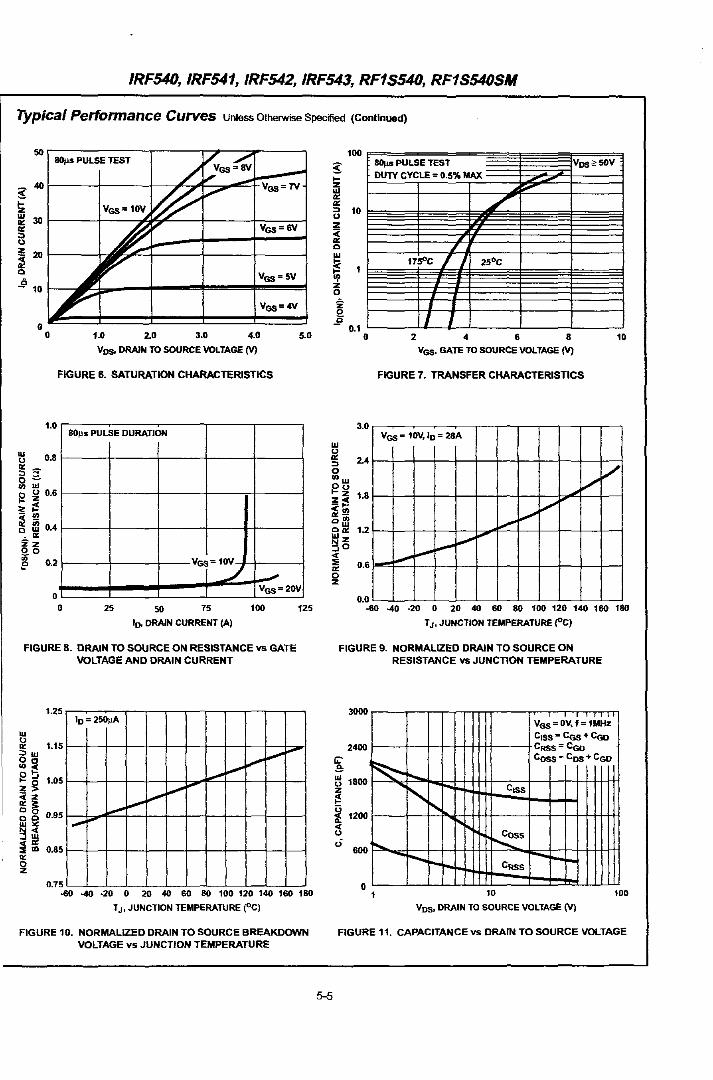
IRF540, IRF541, IRF542, IRF543, RF1S540, RF1S540SM
Typical Performance Curves Unless Otherwise Specified (Continued)
~r-------------,------,~~--~----~ 80jls PULSE TEST
VGS= 5V
VGS=4V
1.0 2.0 3.0 4.0 5.0
VOS. DRAIN TO SOURCE VOLTAGE M
FIGURE 6. SATURATION CHARACTERISTICS
1.0 8O~s PULSE DURATION
VGS= 10V
1,1 -o -' VGS -20V
o 25 ~ 75 100 125
I", DRAIN CURRENT (A)
FIGURE 8. DRAIN TO SOURCE ON RESISTANCE vs GATE VOLTAGE AND DRAIN CURRENT
1.25 ID=2~~
w t>
1.15 '" ~w 00 "'0( O!j
1.05 ~g <tZ "'~ 00 0.95 00 w>< ~< -,w <'" :li 1D 0.85
r" ,.. .....
i,.....-,..
i--"" ". ~ ~ ......
I ..... -'" 0 z
0.75 -60 -40 -20 0 20 40 60 80 100 120 140 160 180
TJ. JUNCTION TEMPERATURE ("C)
FIGURE 10. NORMALIZED DRAIN TO SOURCE BREAKDOWN VOLTAGE vs JUNCTION TEMPERATURE
~ ... z ll! '"
100
~ 10 z ~ o w lc ~ z o
1 0.1
o
3.0
w u
'" 2.4 OJ 0 "w 00 I-z 1.8 ~~ ~~ ~m 1.2 W z ':lo < :Ii 0.6 a: 0 z
0.0
80jls PULSE TEST VOS:>SOV DUTY CYCLE = 0.5% MAX
.Jt.~
/"
/ 17s"c I I 2SoC
I
I J 2 4 6 8 10
VGS. GATE TO SOURCE VOLTAGE (V)
FIGURE 7. TRANSFER CHARACTERISTICS
VGS = 10V. 10 = 26A
V ,/
",. V ",. ,.. "
...... ...... ...-
-60 -40 -20 0 20 40 60 80 100 120 140 160 180
5-5
T J. JUNCTION TEMPERATURE ("C)
FIGURE 9. NORMALIZED DRAIN TO SOURCE ON RESISTANCE vs JUNCTION TEMPERATURE
3000 V~= Ov, f= lMH
II
z C,ss - CGS + Coo
2400 CRSS=CGO
ii:' .eo ... 1800 u z i! ~ 1200 <
~ Coss "" Cos + eGD
I'-..
"'I'. 1'00 C'SS
..... I'
0 c.i
600 " ~oss
r--. .... CRSS -o
1 10
Vos. DRAIN TO SOURCE VOLTAGE (V)
100
FIGURE 11. CAPACITANCE vs DRAIN TO SOURCE VOLTAGE

IRF540, IRF541, IRF542, IRF543, RF1S540, RF1S540SM
Typical Performance Curves Unless Otherwise Specified (Continued)
~r------------------.-----r-----' Vos ~ 5OV,80j.lS PULSE TEST
~ 16r------r------r_--~~~~--r_----~ w u z ~ g 12r------t~~--r---_=~~--~~----~ Q z o u
~ 8r-.F--~~----r_----_+------r_----~
4~~--+_----4_----~----_+----~
O~ ____ ~ ____ _L ____ _L ____ ~ ____ ~
o 10 30 40
1000
~ !z ~ '" ~ 100 z ~ Q
g w 10 ~ :::> o /II
C .!!'
1
175"c -'"
//2soc
I
I I o 0.6 1.2
~
1.8
... ...
2.4 ID, DRAIN CURRENT (A) Vso. SOURCE TO DRAIN VOLTAGE M
FIGURE 12. TRANSCONDUCTANCe vs DRAIN CURRENT FIGURE 13. SOURCE TO DRAIN DIODE VOLTAGE
20
~ lo=28A
w Vos= 50V
" ~ 16
g w I.J
12
'" :::> 0 III a g w !;(
4 " .. ~
0 0 12 24 36 48 60
ag. TOTAL GATE CHARGE (nC)
FIGURE 14. GATE TO SOURCE VOLTAGE vs GATE CHARGE
5-6
3.0

IRF540, IRF541, IRF542, IRF543, RF1S540, RF1S540SM
Test Circuits and Waveforms
VARY tp TO OBTAIN
REQUIRED PEAK lAS
VGS
FIGURE 15. UNCLAMPED ENERGY TEST CIRCUIT
+
FIGURE 17. SWITCHING TIME TEST CIRCUIT
0.2)lf
O~(REFI
Vos (ISOLATED SUPPLy)
SAME TYPE ASDUT
OUT
Vos _ IOCURRENT - SAMPLING
RESISTOR
FIGURE 19. GATE CHARGE TEST CIRCUIT
5-7
o
BVoss
- tp
lAS / ----,/ Voo / \
/ \
FIGURE 16. UNCLAMPED ENERGY WAVEFORMS
-- to(ONI
Vos -!-'--..! 90% ,
0--
FIGURE 18. RESISTIVE SWITCHING WAVEFORMS
IG(REF)
, .. .... Vos .. , .. ,,------------
O~ FIGURE 20. GATE CHARGE WAVEFORMS
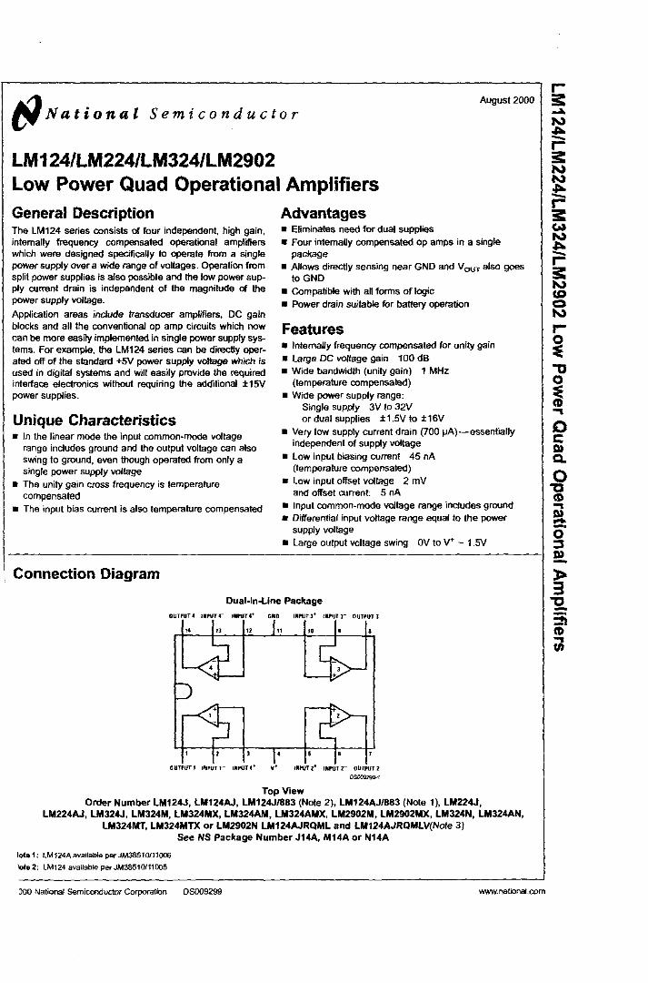
(J1National Semiconductor August 2000
LM124/LM224/LM324/LM2902 Low Power Quad Operational Amplifiers General Description The lM124 series consists of four independent, high gain, intemally frequency compensated operational amplifiers which were designed specifically to operate from a single power supply over a wide range of votlages. Operation from split power supplies is also possible and the low power supply current drain is independent of the magnitude of the power supply voltage.
Application areas include transducer amplifiers, DC gain blocks and all the conventional op amp circuits which now can be more easily implemented in single power supply systems. For example, the lM124 series can be direcUy operated off of the standard +5V power supply votlage which is used in digital systems and will easily provide the required interface electronics without requiring the additional ±lSV power supplies.
Unique Characteristics • In the linear mOde the input common-mode voltage
range indudes ground and the output voltage can also swing to ground, even though operated from only a single power supply voltage
• The unity gain cross frequency is temperature compensated
• The input bias current is also temperature compensated
Connection Diagram
Advantages • Eliminates need for dual supplies • Four intemaNy compensated op amps in a single
package • Allows direCtly sensing near GND and VOUT also goes
toGND • Compatible with an forms of logic • Power drain suitable for battery operation
Features • Intemally frequency compensated for unity gain • large DC voltage gain 100 dB • Wide bandwidth (unity gain) 1 MHz
(temperature compensated) • Wide power supply range:
Single supply 3V to 32V or dual supplies ± 1.SV to ± 16V
• Very low supply current drain (700 ~A)-essentially independent of supply voltage
• Low input biasing current 45 nA (temperature compensated)
• low input offset voltage 2 mV and offset curren!: 5 nA
• Input common-mode voltage range indudes ground • Differential input voltage range equal to the power
supply voltage • large output voltage swing OV to V· - 1.SV
Dual-In-Line Package
OUTPUT' 'ltPUT4- INf"UT4~ GNO IlIl'lJfl+
OUTPUT 1 Il\Ipur ,- INPUT 1+ v" INPUT l" IMPUT r OUTPUT 2
DS00929G-i
Top View Order Number lM124J, lM124AJ, lM124J/883 (Note 2), LM124AJ/883 (Note 1), LM224J,
lM224AJ, lM324J, lM324M, lM324MX, lM324AM, lM324AMX, lM2902M, lM2902MX, lM324N, lM324AN, lM324MT, LM324MTX or LM2902N LM124AJRQML and LM124AJRQMLV{Nofe 3)
lote1: LM124A available perJM38510111006
lote2: LM124 available per JM3851 0111005
See NS Package Number J14A, M14A or N14A
JOO National Semiconductor Corporation 08009299 www.natiOnal.com
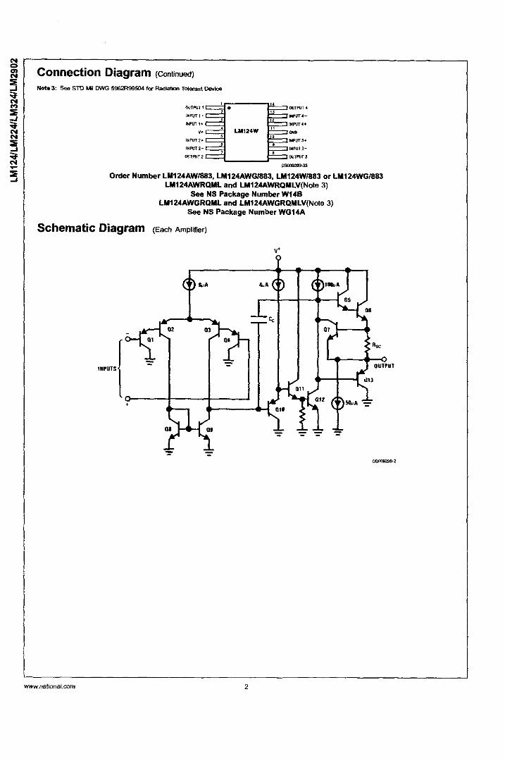
Connection Diagram (Continued)
_ 3: _ sm MI DWG 5962R99504 for Radiation Tolerant Device
OI.lTPtJT I
!/iPIlT1-
INPUT 1+
v. IIiPUT 2+
INPUT 2-
OlIJPUT2 --'-___ ...r-
OUTPUT .01-
INPUT4-
INPUT -4+ ... INPUT 3+
INPUT 3-
OOTPtJT.5
Order Number LM124AW/883, LM124AWGI883, LM124W1883 or LM124WG/883 LM124AWRQML and LM124AWRQMLV(Nole 3)
See NS Package Number W148 LM124AWGRQML and LM124AWGRQMLV(Noie 3)
See NS Package Number WG14A
Schematic Diagram (Each Amplifier)
v'
INPUTS
www.national.com 2
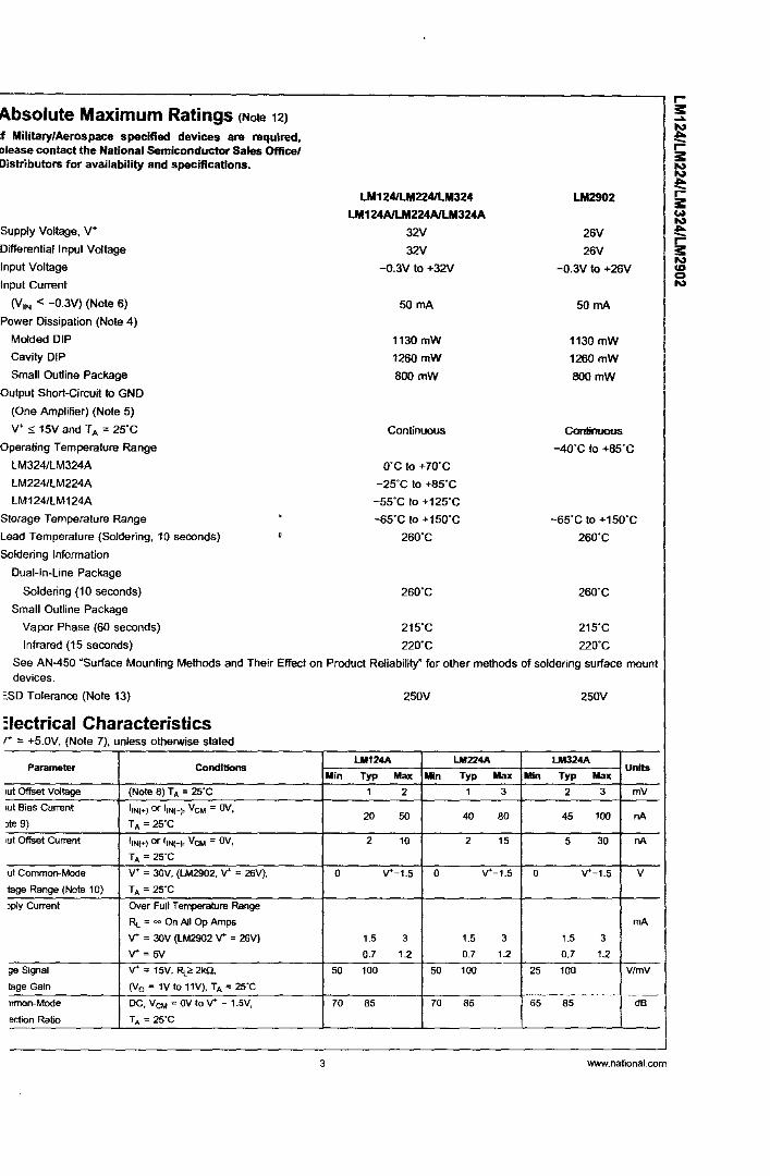
Absolute Maximum Ratings (Note 12)
If Military/Aerospace specified devices are required, please contact the National Semiconductor Sales Office/ Distributors for availability and specifications.
Supply Voltage, V'
Differential Input Voltage
Input Voltage
I nput Current
(V,N < -0.3V) (Note 6)
Power Dissipation (Note 4)
Molded DIP
Cavity DIP
Small Outline Package
o utput Short-Circu~ to GND
(One Amplifier) (Note 5)
V' s 15V and TA = 25'C
o perating Temperature Range
lM324/lM324A
lM2241lM224A
lM124/lM124A
S
l
S
torage Temperature Range
ead Temperature (Soldering, 10 seconds)
oldering Information
Dual-In-line Package
Soldering (10 seconds)
Small Outline Package
Vapor Phase (60 seconds)
Infrared (15 seconds)
. D
LM1241LM2241LM324
LM124A1LM224A1LM324A
32V
32V
-0.3V to +32V
SO rnA
1130 mW
1260 mW
800mW
Continuous
O'C to +70'C
-2S'C to +85'C
-55'C to +125'C
-6S'C to +150'C
260'C
260'C
21S'C
220'C
LM2902
26V
26V
-0.3V to +26V
SO rnA
1130 mW
1260mW
800mW
Continuous
-4Q'C to +85'C
-6S'C to +150'C
260'C
260'C
21S'C
220'C
See AN-4S0 "Surface Mounting Methods and Their Effect on Product Reliability" for other methods of soldering surface mount devices.
::SD Tolerance (Note 13) 2S0V 250V
:Iectrical Characteristics ,. = +S.OV, (Note 7), unless otherwise stated
LM124A LM224A LM324A Parameter Conditions Units
Min Typ Max Min Typ Max Min Typ Max luI Offset Voltage (Note 8) T. = 25'C 1 2 1 3 2 3 mV .ut Bias Current I'N(of-) or I'N(-J' V CM = fN,
20 50 40 80 45 100 nA )Ie 9) T. = 25'C
lut Offset Current I'N(-") or IIN(-), VCM = OV, 2 10 2 15 5 30 nA
TA = 25'C
ut Common-Mode y+ = JOV, (LM2902, y+ = 26V), 0 Y+-l.5 0 Y+-l.5 0 Y+-l.5 V
!age Range (Note 10) T, = 25'C
)pty Current OVer Full Temperature Range
RL = = On All Op Amps rnA
y+ = JOV (LM2902 y+ = 26V) 1.5 3 1.5 3 1.5 3
Y+=5V 0.7 1.2 0.7 1.2 0.7 1.2 ge Signal y+ = 15V, Rc~ 2k!2, 50 100 50 100 25 100 VlmV
tage Gain f% = 1V 10 l1V), TA = 25'C -'--'-'-~-------. -- ---
omon-Mode DC, VCM = OV 10 y+ - 1.5V, 70 85 70 85 65 85 dB
ection Ratio TA = 25'C
3 'IM'W.national.com

Electrical Characteristics (Continued)
y+ ~ +5.0V, (Note 7), unless otherwise stated
LMl24A LM224A LM324A Parameter CondItions Units
Min Typ Max Min Typ Max Min Typ Max
Power Supply V' = 511 to 30V
Rejection Ratio (lM2902, V' = 511 to 26V), 65 100 65 100 65 100 dB
TA = 25'C
Amplifier-to-Amplifier f = 1 kHz to 20 kHz, TA = 25'C -120 -120 -120 dB
Coupflng (Nota 11) (Input Referred)
Output Current Source VIN+::: 1V. VIN = OV. 20 40 20 40 20 40
V' = 1511, Va = 2V, TA = 25'C rnA
Sink VIN ::: 1V, VIN + = av. 10 20 10 20 10 20
V' = 15V. Va = 2V, TA = 25'C
Y,N = 1V. VIN· = OV, 12 50 12 50 12 50 IlA V' = 15V. Va = 200 mY, TA = 25'C
Short Circuit to Ground (Nola 5) V' = 1511, T. = 25'C 40 60 40 60 40 60 rnA
Input Offset Voltage (Nota 8) 4 4 5 mV . -~--- ~. --_ .. .. --~.-- . ---. .........
Vas Drift Rs = on 7 20 7 20 7 30 ~vrc
Input Offset Current IIN(+) - "N(-)' V CM = fJV 30 30 75 nA
los Drift Rs = on 10 200 10 200 10 300 plV'C
Input Bias Current IIN(+) or IIN(-) 40 100 40 100 40 200 nA
Input ComlTlOn-Mode V' = +30V 0 V'-2 0 V'-2 0 V'-2 V
Voltage Range (Nota 10) (lM2902, V' = 26V)
large Signal V' = +15V (VoSwing = 1V to llV)
Voltage Gain Rl2:2k!l 25 25 15 V/mV
Output Voltage VOH V' = 30V Rt.=2kQ 26 26 26 V
Swing (lM2902, V' = 26V) Rt. = 10 kQ 27 28 27 28 27 28
Val V' = 511. Rt. = 10 kQ 5 20 5 20 5 20 mV
Output Current Source Va = 2V VIN+ = +1V, 10 20 10 20 10 20
~~~~~. rnA
Sink VIN = +1V, 10 15 5 8 5 8
V l' = (]V VV' = 15V'
Electrical Characteristics y+ ~ +5.0V, (Note 7), unless otherwise stated
lM1241LM224 LM324 LM2902 Parameter Conditions UnHs
Min Typ Max Min Typ Max Min Typ Max
Input Offset Voltage (Note 8) T. = 25'C 2 5 2 7 2 7 mV
Input Bias Current IIN(+) or I'N{-I' VCM = OV, 45 150 45 250 45 250 nA
(Note 9) T. = 25'C
Input Offset Current IIN(+) or "NH' VCM = OV, 3 30 5 50 5 50 nA
TA = 25'C
Input Common-Mode V' = 3OV. (lM2902. V' = 26V). 0 V' -1.5 0 V'-1.5 0 V' 1.5 V
Voltage Range (Nota 10) TA = 25'C
Supply Current Over Full Temperature Range
Rl = ~ On All OpAmps mA
V' = 30V (LM2902 V' = 26V) 1.5 3 1.5 3 1.5 3
V'=511 0.7 1.2 0.7 1.2 0.7 1.2
large Signal V' - 15V. Rt.o> 2kn. 50 100 25 100 25 100 VlmV
Voltage Gain (VA = 1V to llV), TA = 25'C
Common-Mode ~C. VCM = OV to V' - 1.511. 70 85 65 85 50 70 dB
Rejection Ratio TA = 25'C
Prmer Supply V' = 511 to 30V
Rejection Ratio (LM2902. V' = 5V to 26V). 65 100 65 100 50 100 dB
www.national.com 4
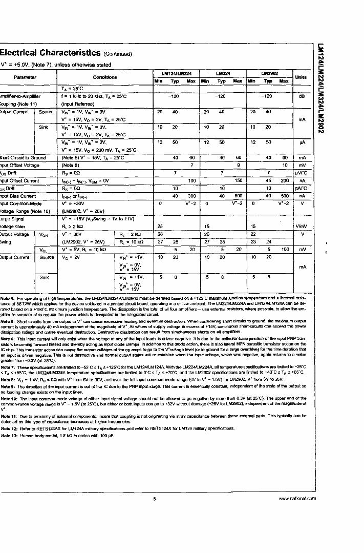
Electrical Characteristics (Continued)
v+ = +5.0V, (Note 7), unless otherwise stated
LM1241LM224 LM324 LM2902 Parameter Conditions Units
Min Typ Max Min Typ Max Min Typ Max
TA = 25'C
I\mplifier -II>-Amplifier f = 1 kHz 10 20 kHz. TA = 25'C -120 -120 -120 dB
::OOpling (No'" 11) (Input Referred)
:Jutput Current Source Y,N + = lV, Y,N = (N, 20 40 20 40 20 40
y+ = 15V, Vo = 2V, TA = 25'C rnA
Sink V'N- = lV, V,N+ = W, 10 20 10 20 10 20
y+ = 15V, Vo = 2V, TA = 25'C
Y,N = lV, V,tt = w, 12 50 12 50 12 50 IIA y+ = 15V, Vo = 200 mV, TA = 25'C
SIlort arcu~ 10 Ground (No'" 5) y+ = 15V, T A = 25'C 40 60 40 60 40 60 mA
nput Offset Voltage (No"'8) 7 9 10 mV
'os Drift Rs = on 7 7 7 ~vrc
nput Offset Current I'N(+) - I'N(-). V CM = OV 100 150 45 200 nA
os Drift Rs = on 10 10 10 pArC
nput Bias Current I'N(+) or I'N(-) 40 300 40 500 40 500 nA
nput Common-Mode y+ = +JOV 0 Y+-2 0 Y+-2 0 Y+-2 V
tollage Range (No'" 10) (LM2902, y+ = 26V)
.arge Signal y+ - +15V (VoSWing = lV to l1V)
toltage Gain RL~2kil 25 15 15 VlmV
)utput Vollage VOH y+ = JOV RL = 21<!l 26 26 22 V
~wing (LM2902, V· = 26V) I Rc = 10 kQ 27 28 27 28 23 24
VOL y+ = 5V, Rc = 10 kQ 5 20 5 20 5 100 mV
)utput Current Source Vo = 2V V,N+ - +1V, 10 20 10 20 10 20
V - = (N, \l' = 15V
rnA
Sink Y,N = +1V, 5 8 5 8 5 8
V + = ov, \l' = 15V
Note4: For operating at high temperatures. the LM3241LM324A1LM2902 must be derated based on a +125"C maximum junction temperature and a thennal rests-tance of sa"C/W which applies for the device soldered in a printed circuit board, operating in a still air ambient. The LM224J1...M224A and LM1241LM124A can be de-rated based on a +150'C maximum junction temperature. The dissipation is the total of all four amplifiers-use external resistors, where possible. to allow the am-plifier to saturate of to reduce the power which is dissipated in the integrated circuit
Note 5: Short circuits from the output to y+- can cause excessive heating and eventua.t destruction. When considering short drcuits to ground, the ma.ximum output current is approximately 40 rnA independent of the magnitude of y+. At values of suppty voltage in excess of +15V, continuous short-cin::uits can exceed the power
dissipation ratings and cause eventual destruction. Destructive dissipation can result from simultaneous shorts on all ampflfiers.
Note 6: This input current will only exist when the voltage at any of the input leads is driven negative. It is due to the rollector--base jwlction of the input PNP tran-sistors beroming forward biased and thereby acting as input diode clamps. In addition to this diode action, there is also lateral NPN parasitic transistor action on the Ie chip. This: transistor action can cause the ou1put voftages of the op amps to go to the v+voftage level (or to ground for a large overdrive) for the time duration that an input is driven negative. This is not destructive and nonnal output states wiD re-establish when the input voltage, which was negative, again returns to a value greater than -O.3V (at 25"C).
Note 7: These specifications are limited to -55"C s: T AS: +12S"C forthe LM124/LM124A With the LM2241LM224A, aU temperature specifications are limited to -25-C :5 TA :5 +B5'C, the LM3241lM324A temperature specifications are limited to O'C s TA S +70·C, and the LM2902 spedfications are limited to -40·C:s TA s +SS·C.
Note 8: Vo "" 1.4V, Rs = on wrth y+ from 5V to 3OV; and over the full input rommon~mode range (OV to y+ - 1.5V) for LM2902, y+ from 5V to 26V.
Note 9: The direction of the input current is out of the IC due to the PNP input stage. This current is essentially constant. independent of the state of the output so
no loading change exists on the input lines.
Note 10: The input cornmon-mode voltage of either input signal voltage should not be allowed to go negative by more than 0.3V (at 2S·C). The upper end of the common~rnode voftage range is y+ - 1.5V (at 25'C), but either or both inputs can geta +32V without damage (+26V forLM29(2), independent of the magnitude of
V'. Note 11: Due to proximity of external components, insure that ooupling is not originating via stray capacitance between these external parts. This typically can be detected as this type of capacitance increases at higher frequencies.
Note 12: Refer to RETS124AX for LM124A military spedfications and refer to RETS124X for LM124 military specifications.
Note 13: Human body modet, 1.5 k.Q in series wrth 100 pF.
5 www.national.com

Typical Performance Characteristics
Input Voltage Range 15r-----,------.-----n
0
:? ~ w <:> < ~ ~ 0 > ~
=> ~
~
z >--H
10
5
o 5 10 15
v+ OR V- - POWER SUPPLY VOLTAGE (tVoc) DSIJ092ll9.34
Supply Current
~ 1 ~ TA' oo~ TO +125 OC
I P T. I -55;C--
ID 20
v+ - SUPPLY VOLTAGE (VI)() 0S009299-36
Open Loop Frequency Response
z '< '-' w <:> ~ ~ o >
www.natlonal.com
10 100 l.Ok 10k lOOk 100M 10~
f - FREQUENCY (Hz) DSOOI2!I9-J8
Input Current 90
80
Jl 70 -5
60
50
40
30
O 0
o
I I Ivcw=OVoc I I I
v+ = +30 Voc I I
v+ = +15 Voc f--- t-
v+ = '5VoC I I 1
I I I -55 -35 -15 5 25 45 65 85 105125
Voltage Gain
~ .. '-' w
160
120
~ 80 '::; o >
o
T. - TEWPERATURE (oc) 0&I092!l<>35
Rc = 20kll
". ~ Rc = 2 kll
10 20 30 40
V+ - SUPPLY VOLTAGE (Voc ) DSOO9299-37
Common Mode Rejection Ratio
= ~ 120
0 >= ;:, 100 z 0 >= 8 ;:J ~
w 0 0
'" , z 0
'" '" 0 0
~ ~
'" 100 1. u 10k lOOk 1M
f - FREQUENCY (Hz)
6

BIODATA
Nama Y ohanes Pandu A.
NRP 5103099059
Tempat, Tgl. Lahir Surabaya, 14-05- 1979
Agama Katolik
Alamat rumah Jl. Mastrip Warugunung
IX /51 Surabaya
Riwayat Pendidikan :
• Tahun 1992 Lulus SDK Indriyasana VII, Surabaya.
• Tahun 1995 Lulus SL TK Santo Yosef, Surabaya.
• Tahun 1998 Lulus SMUK. St. Loui.s U, SUIabaya
PER PUS T A ~ A A N l Universitas Kato.k \'y 1,,'.1 1i'J.Cl •• !.l..lla
l SUKAllAYA )