“o” subscript denotes the equilibrium carrier concentration. ideal diode equation
TRANSCRIPT

“o” subscript denotes the equilibrium carrier concentration.
Ideal diode equation
material. type-nin ion concentrat hole mequilibriu
material. type-pin ion concentrat hole mequilibriu
material. type-pin ion concentratelectron mequilibriu
material. type-nin ion concentratelectron mequilibriu
no
po
po
no
p
p
n
n
2. inpn

At equilibrium case ( no bias )
Ideal diode equation
)2(.
)1(.
.
2
2
2
materialtypepnpn
materialtypennpn
npn
ipopo
inono
i

Ideal diode equation
2
22
ln assuming full ionization
; majority carriers
.ln . for n-type
ln exp (3)
A Dbi
i
A po D no
po nobi no no i
i
po bibi po no
no
kT N NV
q n
N p N n
p nkTV n p n
q n
p qVkTV p p
q p kT

Ideal diode equation
22
, (2)
.ln .
ln exp (4)
po nobi po po i
i
no bibi no po
po
Similarly from equation
p nkTV n p n
q n
n qVkTV n n
q n kT
This equation gives us the equilibrium majority carrier concentration.

Ideal diode equation
What happens when a voltage appears across the p-n junction ?
Equations (3) and (4) still valid but you should drop (0) subscript and change Vbi with
i. Vbi – VF if a forward bias is applied.
ii. Vbi + VR if a reverse bias is applied.
VF : forward voltage
VR : reverse voltage
With these biases, the carrier densities change from equilibrium carrier densities to non- equilibrium carrier densities.
Ideal diode equation
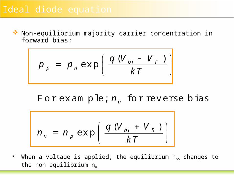
Non-equilibrium majority carrier concentration in forward bias;
( )exp
For example; for reverse bias
( )exp
bi Fp n
n
bi Rn p
q V Vp p
kT
n
q V Vn n
kT
• When a voltage is applied; the equilibrium nno changes to the non equilibrium nn.

Assumption; low level injection
• For low level injection; the number of injected minorities is much less than the number of the majorities. That is the injected minority carriers do not upset the majority carrier equilibrium densities.
pop
non
pp
nn
• Non equilibrium electron concentration in n-type when a forward bias is applied ,
( )exp non-equilibrium.bi F
n p
q V Vn n
kT

Ideal diode equation
( ) (5)
exp (6)
bi Fn no no p
bino po
q V Vn n n n
kT
qVn n
kT
combining (5) and (6)
( )exp expbi F bi
p po
q V V qVn n
kT kT

Ideal diode equation
poexp and subtracting n from both sides
exp 1
the excess concentration of minority electrons
over the equilibrium concentration at the edge of the DR
Fp po
p po po n
n
qVn n
kT
qVn n n
kT
Solving for non-equilibrium electron concentration in p-type material, i.e. np

Ideal diode equation
Similarly ,
exp 1 the non-equilibriumn no no p
qVp p p
kT
the excess concentration of minority holes
over the equilibrium concentration at the edge of the DR
p

Forward-bias diode; injection of minority carriers across DR
+ -
p n++
--
B
pno
npo
A
nno
ppo
point A
point B
p po
n no
n n
p p
lnlp
• is the distance from DR edge into p-side
• is the distance from DR edge into n-side
p
n
l
l
When a forward bias is applied; majority carriers are injected across DR and appear as a minority carrier at the edge of DR on opposite side. These minorities will diffuse in field free opposite-region towards ohmic contact. Since ohmic contact is a long way away, minority carriers decay exponentially with distance in this region until it reaches to its equilibrium value.

Exponential decay of injected minority carriers on opposite sides
The excess injected minorities decay exponentially as
p
( ) (0)exp
( ) (0)exp
and L are diffusion lengths
for electrons and holes
pp
n
nn
p
n
lp l n
L
ln l p
L
L

Number of Injected Minority Holes Across The Depletion Region
• By means of forward-biasing a p-n junction diode, the holes diffuse from left to right accross the DR and they become minority carriers.
• These holes recombine with majority electrons when they are moving towards ohmic constants.
• So, the number of minority holes on the n-region decreases exponentially towards the ohmic contact. The number of injected minority holes;excess holes;
( ) (0)exp( )nn
p
lp l p
L
Distance into then region from the Depletion Region
Diffusion Length for holes

Number of Injected Minority Holes Across The Depletion Region
point A
( ) (0)exp( )
(0) exp( ) 1
(0) exp 1
p po
pp
n
po
no
n n
ln l n
L
qVn n
kT
qVp p
kT

Ideal diode equation
• Similarly by means of forward biasing a p-n junction, the majority electrons are injected from right to left across the Depletion Region. These injected electrons become minorities at the Depletion Region edge on the p-side, and they recombine with the majority holes. When they move into the neutral p-side, the number of injected excess electrons decreases exponentially.
)exp(1)exp()(
)exp()0()(
n
ppopn
n
pnpn
L
l
kT
qVnl
L
ll

Ideal diode equationDiffusion current density for electrons ;
( ) exp 1 exp
( 0) exp 1 Minus sign shows that electron current
density is
n po pn n n p
n n
n pon p
n
D n ldn d qVJ qD qD n l q
dx dx L kT L
qD n qVJ l
L kT
in opposite direction to increasing .That is in the positive x direction.
Similarly for holes;
pl
( 0) exp 1
The total current density;
exp 1
p nop n p
p
n po p noTotal n p
n p
qD pdp qVJ l qD
dx L kT
D n D p qVJ J J q
L L kT

Ideal diode equation
exp 1 exp 1
multiplying by area ;
exp 1
n po p noTotal o
n p
o
D n D p qV qVJ q J
L L kT kT
qVI I
kT
Ideal diode equation
This equation is valid for both forward and reverse biases; just change the sign of V.

Ideal diode equation
• Change V with –V for reverse bias. When qV>a few kT; exponential term goes to zero as
VB I0
VB ; Breakdown voltage
I0 ; Reverse saturation current
Forward Bias
Reverse Bias
oII Reverse saturation currentexp 1o
qVI I
kT
Current
Voltage

Forward bias current densities
+ -
p n
ln=0lp=0
Ohmic contact
pntotal JJJ
pJnJ
Cur
rent
den
sity
Jtotal is constant through the whole diode.
Minority current densities decreases exponentially into the the neutral sides whereas the current densities due to the majorities increase into the neutral sides.

p-n junction in reverse bias
• Depletion region gets bigger with increasing reverse bias.
• Reverse bias prevents large diffusion current to flow through the diode.
• However; reverse bias doesn’t prevent the small current flow due to the minority carrier. The presence of large electric field across the DR extracts almost all the minority holes from the n-region and minority electrons from the p-region.
• This flow of minority carriers across the junction constitudes I0, the reverse saturation current.
• These minorities are generated thermally.
- +
p n
ln=0lp=0
pntotal JJJ
pJnJCur
rent
den
sity
Car
rier
dens
ity
pn
np
pnonpo

p-n junction in reverse bias
• The flow of these minorities produces the reverse saturation current and this current increases exponentially with temperature but it is independent of applied reverse voltage.
Vb I0
VB ; Breakdown voltage
I0 ; Reverse saturation current
Forward Bias
Reverse BiasDrift current
I(current)
V(voltage)

Junction breakdown or reverse breakdown
• An applied reverse bias (voltage) will result in a small current to flow through the device.
• At a particular high voltage value, which is called as breakdown voltage VB, large currents start to flow. If there is no current limiting resistor which is connected in series to the diode, the diode will be destroyed. There are two physical effects which cause this breakdown.
1) Zener breakdown is observed in highly doped p-n junctions and occurs for voltages of about 5 V or less.
2) Avalanche breakdown is observed in less highly doped p-n junctions.

Zener breakdown
• Zener breakdown occurs at highly doped p-n junctions with a tunneling mechanism.
• In a highly doped p-n junction the conduction and valance bands on opposite side of the junction become so close during the reverse-bias that the electrons on the p-side can tunnel from directly VB into the CB on the n-side.
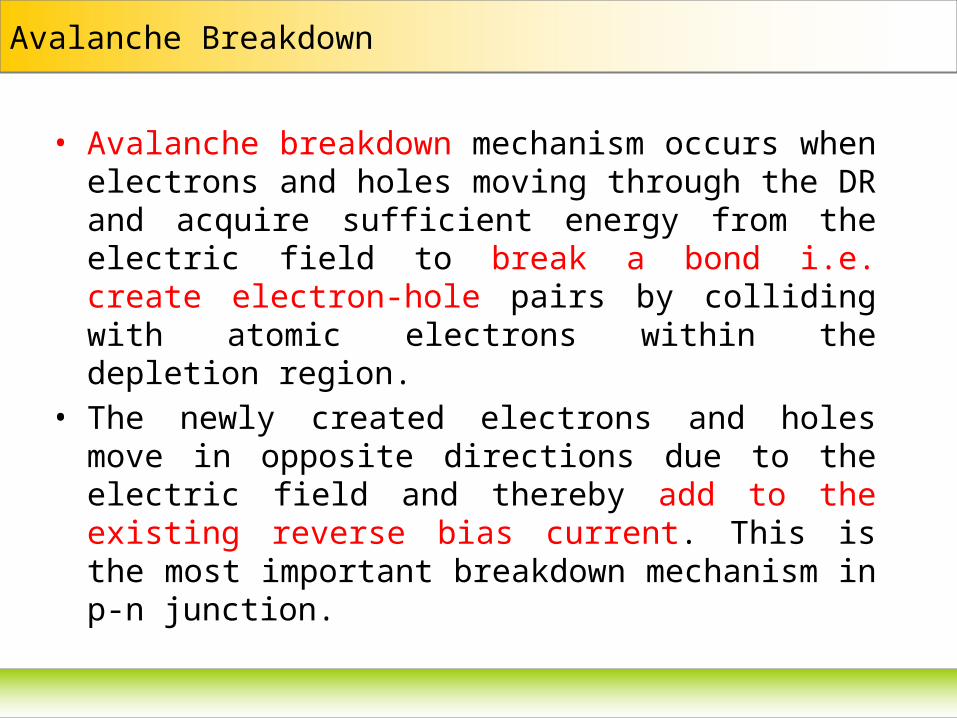
Avalanche Breakdown
• Avalanche breakdown mechanism occurs when electrons and holes moving through the DR and acquire sufficient energy from the electric field to break a bond i.e. create electron-hole pairs by colliding with atomic electrons within the depletion region.
• The newly created electrons and holes move in opposite directions due to the electric field and thereby add to the existing reverse bias current. This is the most important breakdown mechanism in p-n junction.

p – n junction
There is a big discontinuity in the fermi level accross the p-n junction.
EC
Eİ
EV
Ef
EC
Eİ
EV
Ef
EC
Eİ
EV
Ef
p-type n-typeEC
Eİ
EV
Ef
p-type n-type