01-使用stm32 设计hmi(硬件) v1
TRANSCRIPT

使用STM32 设计HMI-硬件介绍使用STM32提供的硬件资源和软件资源开发人机交互界面HMI的方法

Agenda一、STM32 HMI设计硬件资源
LCD controller
ChromeART accelerator
SDRAM interface
二、 STM32 HMI设计软件资源STemWin
IS2T
TouchGFX
2

Embedded graphics on STM32F4

OBJECTIVES
• Getting familiar with basics of graphics• General LCD connection
• Color representation
• Layers
• Transparency / alpha channels
• CLUT
• Color keying
• Understand how you can benefit from STM32F4’s HW acceleration• Usage of LTDC layer features
• Offload CPU by using Chrom-ART
• Hardware pixel format conversion
4
4

CORTEX M4 CPU+ MPU
+ FPU180 MHz
5STM32F4x9 Block Diagram
256KB SRAM
AP
B2
(max
90M
Hz)
3x 12-bit ADC24 channels / 2Msps
3x I2C
80/112/140 I/Os
Up to 16 Ext. ITs
2x6x 16-bit PWM Synchronized AC Timer
2x Watchdog(independent & window)
5x 16-bit Timer
JTAG/SW Debug
XTAL oscillators32KHz + 8~25MHz
Power SupplyReg 1.2V
POR/PDR/PVD
DMA16 Channels
Nested vect IT Ctrl
2x DAC + 2 Timers
2 x USART/LIN
4 x SPI
Bridge
Bridge
1 x Systic Timer
PLLClock Control
RTC / AWU
APB1
(max 45MHz)
4KB backup RAM
ETM
Ethernet MAC 10/100, IEEE1588
Fla
sh I
/F
2MB Flash Memory Dual
Bank
External Memory Interface with SDRAM
Encryption
Camera Interface
USB 2.0 OTG FS
6x USART/LIN
1x SDIO
Int. RC oscillators32KHz + 16MHz
AHB1
(max 180MHz)
AHB2
(max 180MHz)
3 x 16bit Timer
AR
M ®
32-b
it m
ulti-
AH
B b
us m
atrix
A
rbite
r (m
ax 1
20M
Hz)
2x 32-bit Timer
2x CAN 2.0B
2x SPI/I2S
Temp Sensor
LCD Controller
Chrom-ART
1xSAINew IPs/Features/more IPs instances
• Fully compatible with F4x
• Up to 180MHz with over-drive mode
• Dual Bank 2 x 1MB Flash
• 256KB SRAM
• FMC with SDRAM + Support and 32-bit data
• Audio PLL + Serial Audio I/F
• LCD-TFT Controller
• Chrom – ART Accelerator
• Hash: supporting SHA-2 and GCM
• More serial com and more fast timers running at Fcpu
• 100 pins to 208 pins
• 1.71V-3.6V Supply
USB 2.0 OTG HS

System Architecture 6
SRAM1112KBSRAM1112KB
SRAM216KB
SRAM216KB
SRAM3 64KB
SRAM3 64KB
AHB1AHB1
CORTEX-M4180MHz
FPU & MPU
Master 1
CORTEX-M4180MHz
FPU & MPU
Master 1
D-Code
Dual PortDMA2
Master 3
Dual PortDMA2
Master 3
FIFO/8 StreamsFIFO/8 Streams
AHB2AHB2
Dual P
ortA
HB
1-AP
B1
Dual P
ortA
HB
1-AP
B1
Dual PortDMA1
Master 2
Dual PortDMA1
Master 2
FIFO/8 StreamsFIFO/8 Streams
CCM data RAM
64KB
CCM data RAM
64KB
High SpeedUSB2.0Master 5
High SpeedUSB2.0Master 5
FIFO/DMAFIFO/DMA
Ethernet 10/100Master 4
Ethernet 10/100Master 4
FIFO/DMAFIFO/DMA
AR
TA
ccel
erat
orA
RT
Acc
eler
atorI-Code
2Mbytes Flash
Bank1
1Mbytes
Bank1
1Mbytes
Bank2
1Mbytes
Bank2
1Mbytes
FMCFMC
LCD-TFT
Master 6
LCD-TFT
Master 6
FIFOFIFO
DMA2D
Master 7
DMA2D
Master 7
FIFOFIFO
D-B
us
S-B
us
I-B
us
Dual P
ortA
HB
1-AP
B2
Dual P
ortA
HB
1-AP
B2
Multi-AHB Bus Matrix
Graphics on STM32

Image quality needs
• iPhone has completely changed the required level of graphical quality
• Bigger display size
• Better display resolution
• Perfect icons
• State of the art animations (coverflow…etc…)
• User wants the same experience than on iPhone• Huge resource needs on microcontroller side
• Hardware acceleration becomes mandatory
• Content design/creation is a key aspect
• But no need for a gaming machine• No need for real 3D : 2D graphics is wide enough
8

Overview
• Past / TodayPast / TodayPast / TodayPast / Today
• Keyboard and/or Knob
• Optional 7-segment display
• Optional dot-matrix display
(text or graphical)
• Limited interactivity
9

Typical embedded display needs
• For home appliance• Display size and form factor will be very different from an equipment to another
• In most of them we shall not be above 6~7 inches
• iPad 2 display is 132PPI (pixels per inch)
• 7” 4:3 display 800x600 represents @142PPI
10

From ones and zeros to image display 11
Font 1
Text 1
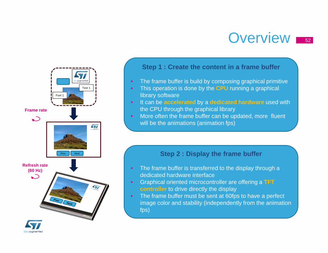
Step 2 : Display the frame buffer
• The frame buffer is transferred to the display through a dedicated hardware interface
• Graphical oriented microcontroller are offering a TFT controller to drive directly the display
• The frame buffer must be sent at 60fps to have a perfect image color and stability (independently from the animation fps)
Step 1 : Create the content in a frame buffer
• The frame buffer is build by composing graphical primitive• This operation is done by the CPU running a graphical
library software• It can be accelerated by a dedicated hardware used with
the CPU through the graphical library• More often the frame buffer can be updated, more fluent
will be the animations (frames per second / fps)
NextPrev
Refresh rate (60 Hz)
Frame rate

STM32F4x9 Architecture
• TFT controller allows the interfacing • Chrome-ART ( DMA2D) provides a true HW graphical acceleration• DMA2D offloads the CPU for operations like rectangle filling, rectangle
copy (with or without pixel format conversion), and image blending• DMA2D goes faster than the CPU for the equivalent operation
TFTController
InternalFlash
InternalSRAM
ExternalMemory
Controller
Chrom-ART Accelerator
(DMA2D)Cortex-M4
Bus Matrix
External memory
12
Implementation examples and resources requirements
13
13

Image Building process 14Using STM32F4x7/4X9 internal RAM (192K) for
small resolutions
Double buffer : New image and Frame buffers can be in internal RAMSingle buffer : 2 options:• Image can be handled by regions: one region to be displayed while the other is been built and so only one buffer will be needed
• new image buffer in internal RAM and frame buffer in external RAM or in display internal memory.
External memory needed for both frame buffer and new image buffer
BUFFER SIZES
(Kbytes) ↘
CGA
(320x200)
QVGA
(320x240)
WQVGA
(480x272)
VGA
(640x480)
WVGA
(800x480)
SVGA
(800x600)
XGA
(1024x768)
1 (2 colors) 7,8 9,4 15,8 37,5 46,9 58,6 96,0
2 (4 colors) 15,6 18,8 31,6 75,0 93,8 117,2 192,0
bpp ↓ 4(16 colors) 31,3 37,5 63,3 150,0 187,5 234,4 384,0
8 (256 colors) 62,5 75,0 126,6 300,0 375,0 468,8 768,0
16 (high color) 125,0 150,0 253,1 600,0 750,0 937,5 1536,0
24 (true color) 187,5 225,0 379,7 900,0 1125,0 1406,3 2304,0
32 (deep
color) 250,0 300,0 506,3 1200,0 1500,0 1875,0 3072,0

Single Chip MCU
•Internal Flash up to 2MB
•Internal SRAM up to 256KB• Frame buffer in internal SRAM
• 16-bit QVGA (320 x 240 ~154 KB)• 8-bit WQVGA (400 x 240 ~97 KB)
•Package LQFP 100pin
16-bit QVGA, 8-bit WQVGA
STM32F4x9
Cost saving + Graphic Acceleration
TFTController
InternalFlash
InternalSRAM
ExternalMemory
Controller
Chrom-ART AcceleratorCortex-M4
Bus Matrix
15

MCU with External Memory
•Internal Flash up to 2MB
•Internal SRAM up to 256KB
•External Memory for frame buffer • 16-bit or 32-bit SDRAM / SRAM
•Package: LQFP 144pin, up to 208.
16
Up to SVGA ( 800x600 )
STM32F4x9
Unique Graphical Capability and
Flexible architecture
TFTController
InternalFlash
InternalSRAM
ExternalMemory
Controller
Chrom-ART AcceleratorCortex-M4
Bus Matrix
SDRAM

Which package to use depending on the variant targeted?
Variant TFT Controller External Memory - SDRAM STM32F4x 9 package
High-End Yes 32-bit LQFP208/BGA216
Mid-End Yes 16-bitLQFP144/
BGA176 / LQFP176
Low-End
No No LQFP100/LQFP144
Yes No LQFP100/LQFP144
SDRAM devices example:• MT48LC4M16A2P-7E : 64Mb • MT48LC16M16A2P-7E : 256Mb
17

LCD-TFT Display Controller (LTDC)MCD Application Team

Benefits
• AHB bus Master• Can access any part of address space → ext. memory, internal SRAM, Flash.
• Flexible programmable display parameters• Display control signals
• Flexible color format
• Multi-Layer Support • Windowing
• Blending
• Flexible programmable parameters for each Layer
• On chip memory or External memory can be used as Frame buffer
19

LCD-TFT architecture 20
AH
B M
aste
r Int
erfa
ce
LCD_G[7:0]
LCD_B[7:0 ]
Layer2
FIFO
64x32b
AH
B In
terf
ace
Con
figur
atio
n an
d
stat
us r
egis
ters
LCD_CLK
LCD_HSYNC
LCD_VSYNC
LCD_DE
LCD_R[7:0 ] LCD
Pan
elBlending
PFC
PFC
Layer1
FIFO
64x32b
Synchronous Timings Generation
AP
B In
terf
ace
Dithering
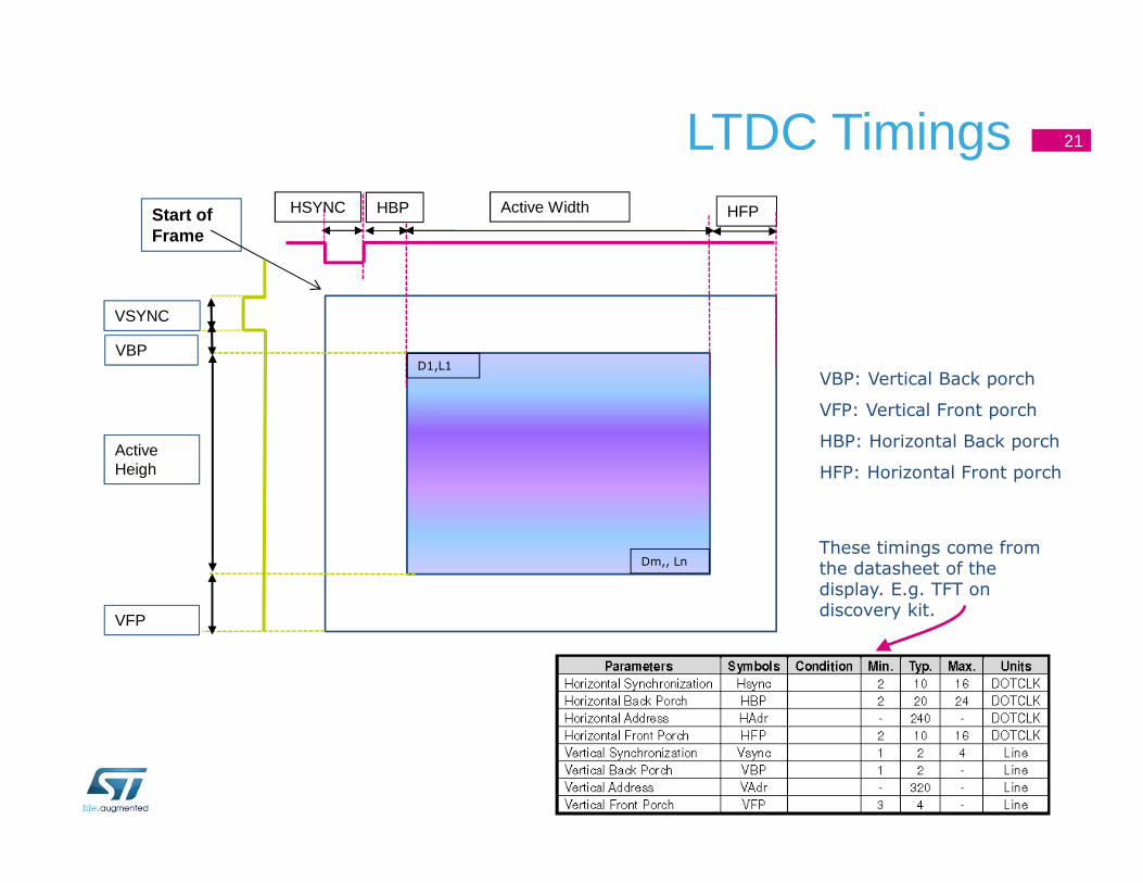
LTDC Timings 21
8/12/2015
D1,L1
Dm,, Ln
HFPHBP
VBP
VFP
VBP: Vertical Back porch
VFP: Vertical Front porch
HBP: Horizontal Back porch
HFP: Horizontal Front porch
Start of Frame
VSYNC
HSYNC Active Width
Active Heigh
These timings come from the datasheet of the display. E.g. TFT on discovery kit.

Frame Display
VSYNC Vertical Back Porch (VBP)
LCD Lines Vertical Front Porch (VFP)
22
HSYNC Horizontal(VBP)
LCD Columns Horizontal(HFP)
LCD_CLK
LCD RGBs
LCD Data Enable
1 Line
1 Frame
1 2 3 4 5 x x x x 480x
Vertical/Horizontal transactions
• Horizontal transaction
23
• Vertical transactionStart of Frame
Start of Scan Line
LCD basic timing signals
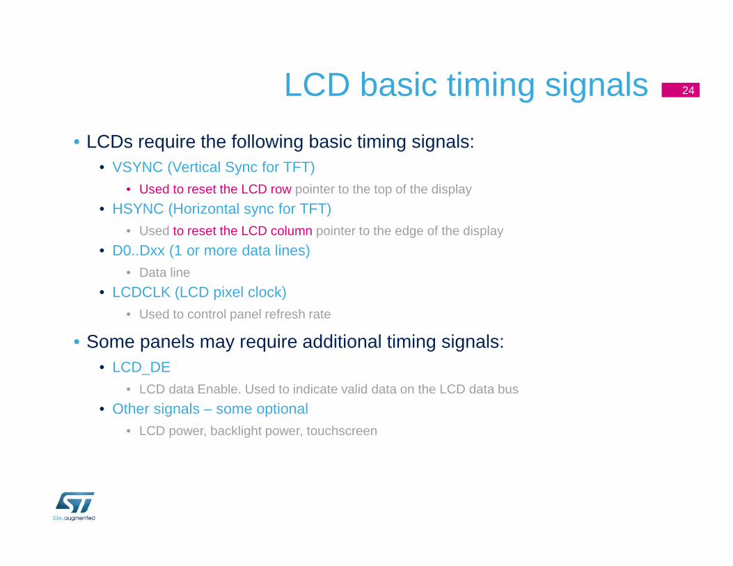
• LCDs require the following basic timing signals:• VSYNC (Vertical Sync for TFT)
• Used to reset the LCD row pointer to the top of the display
• HSYNC (Horizontal sync for TFT)
• Used to reset the LCD column pointer to the edge of the display
• D0..Dxx (1 or more data lines)
• Data line
• LCDCLK (LCD pixel clock)
• Used to control panel refresh rate
• Some panels may require additional timing signals:• LCD_DE
• LCD data Enable. Used to indicate valid data on the LCD data bus
• Other signals – some optional
• LCD power, backlight power, touchscreen
24

LCD Memory Requirements
• Frame buffer size• The panel size and bits per pixel determine the amount of memory
needed to hold the graphic buffer.
• Memory Requirement (KB) = (bpp * Width * Height)/8
25
Panel Resolution Total Pixel bpp (bit per pixel) Requir ed memory (KB)
320x240 (QVGA) 76.8K 16bpp 153.6
8bpp 76.8
480x272 (WQVGA)
130.5K 16bbp 261.12
640x480 (VGA) 307.2K 16bbp 614.4
• In many cases, more memory is needed. E.g. double buffering: one graphic buffer to store the current image while a second buffer used to prepare the next image.
LTDC Clocks and reset
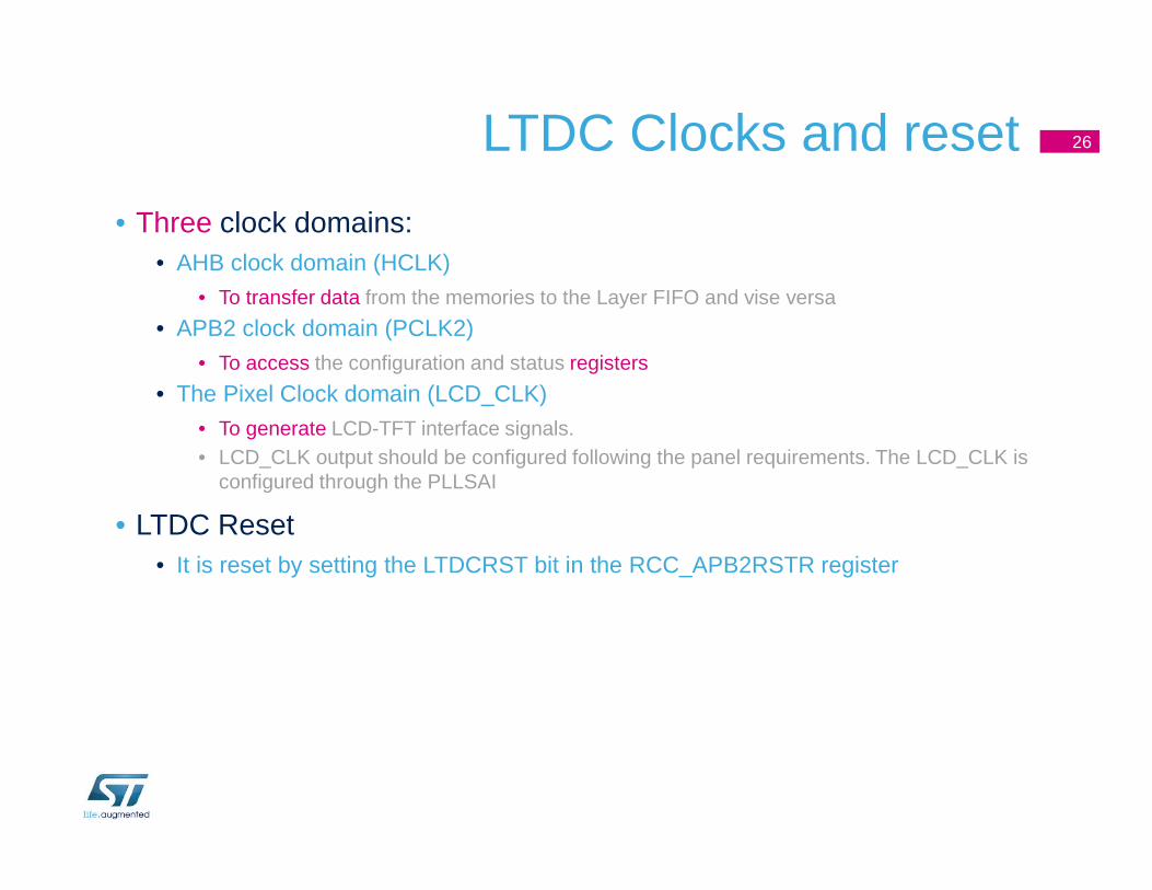
• Three clock domains:• AHB clock domain (HCLK)
• To transfer data from the memories to the Layer FIFO and vise versa
• APB2 clock domain (PCLK2)
• To access the configuration and status registers
• The Pixel Clock domain (LCD_CLK)
• To generate LCD-TFT interface signals. • LCD_CLK output should be configured following the panel requirements. The LCD_CLK is
configured through the PLLSAI
• LTDC Reset• It is reset by setting the LTDCRST bit in the RCC_APB2RSTR register
26
LCD-TFT Signals
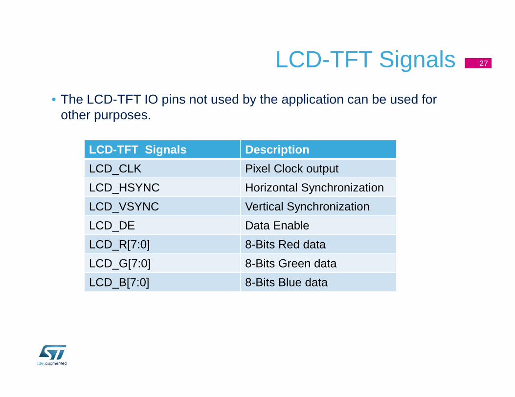
• The LCD-TFT IO pins not used by the application can be used for other purposes.
27
LCD-TFT Signals Description
LCD_CLK Pixel Clock output
LCD_HSYNC Horizontal Synchronization
LCD_VSYNC Vertical Synchronization
LCD_DE Data Enable
LCD_R[7:0] 8-Bits Red data
LCD_G[7:0] 8-Bits Green data
LCD_B[7:0] 8-Bits Blue data

LTDC Main Features - (1/3)
• 24-bit RGB Parallel Pixel Output; 8 bits-per-pixel ( RGB888)
• AHB 32-Bit master with burst access of 16 words to any system memory
• Dedicated FIFO per Layer (depth of 64 word)
• Programmable timings to adapt to targeted display panel.• HSYNC width, VSYNC width, VBP, HBP, VFP, HFP
• Programmable Polarity of:• HSYNC, VSYNC, Data Enable
• Pixel clock
• Supports only TFT (no STN)
28
LTDC Main Features - (2/3)
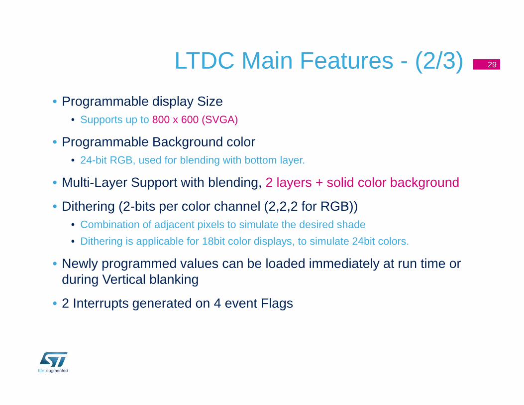
• Programmable display Size• Supports up to 800 x 600 (SVGA)
• Programmable Background color• 24-bit RGB, used for blending with bottom layer.
• Multi-Layer Support with blending, 2 layers + solid color background
• Dithering (2-bits per color channel (2,2,2 for RGB))• Combination of adjacent pixels to simulate the desired shade
• Dithering is applicable for 18bit color displays, to simulate 24bit colors.
• Newly programmed values can be loaded immediately at run time or during Vertical blanking
• 2 Interrupts generated on 4 event Flags
29

Alpha Channel Usage
• The Alpha channel represent the transparency of a pixel
• It’s mandatory as soon as you are manipulating bitmaps with non square edges or for anti-aliased font support
30
Aliased Anti-aliased
• 0xFF = opaque 0xFFFF0000 0xAA FF0000 0x30FF0000
Box filled with color in ARGB8888 format

Pixel Data Mapping vs Color Format
Ax+1[3:0] Rx+1[3:0] Gx+1[3:0] Bx+1[3:0] Ax[3:0 ] Rx[3:0] Gx[3:0] Bx[3:0]
31
7:015:823:1631:24
ARBG8888
RGB888
ARGB4444
AL88 Ax+1[7:0] Lx+1[7:0] Ax[7:0] Lx[7:0]
Bx+1[7:0] Rx[7:0] Gx[7:0] Bx[7:0]
Ax[7:0] Rx[7:0] Gx[7:0] Bx[7:0]
Ax+3[3:0] Lx+3[3:0]
Ax+2[3:0] Lx+2[3:0] Ax+1[3:0] Lx+1[3:0] Ax[3:0] Lx[3: 0]AL44
Lx+3[7:0] Lx+2[7:0] Lx+1[7:0] Lx[7:0]L8
Ax+1[0]
Rx+1[4:0]
Gx+1[4:3]
Gx+1[2:0] Bx+1[4:0] Ax[0] Rx[4:0] Gx[4:3] Gx[2:0] Bx[4:0]ARGB1555
Rx+1[4:0] Gx+1[5:3] Gx+1[2:0] Bx+1[4:0] Rx[4:0] Gx[5:3] G x[2:0] Bn[4:0]RGB565
32
24
16
16
16
8
16
8
bpp8 programmable Input color format per layer

Pixel Format Conversion
• The color format of a bitmap converted into another one : this operation is called Pixel Format Conversion (PFC)
• Direct Mode to Direct Mode or Indirect Mode to Direct Mode is easy to do, but converting to an indirect color format would mean regenerating a CLUT which is a very complex operation...
32
0 0 0 00 0 0 0
0 4 3 24 3 2 1
0 4 3 24 3 2 1
0 4 3 24 3 2 1
0
04 3 2 1
04 3 2 1
04 3 2 1
PFC
ARGB1555 ARGB8888

PFC - Direct color Mode 33
A R G B
32-bit per pixel
ARGB8888
24-bit per pixel
RGB888
16-bit per pixel
ARGB4444ARGB1555
RGB565
Direct coding

PFC - Indirect color Mode 34
A R G B
8-bit per pixel
L8AL44
A8
4-bit per pixel
L4A4
16-bit per pixel
AL88
Indirect codingA R G B
A R G B
...
ColorLookUp Table
Index
A R G B
0x00
0x01
0xFF

CLUT - Palletized color
• Color Look-Up Table (CLUT) up to 256 entry per layer
• The frame buffer will contain an index value for each pixel
• The CLUT must be pre-loaded with RGB values for each index
• Each RGB value is stored in a position in the CLUT.
• The CLUT must be reloaded only when LTDC is disabled or during vertical blanking period
• The CLUT can be enabled on the fly for every layer through the LTDC_LxCR register
35

CLUT- Palletized
• The R, G and B values and their own respective address are programmed through the LTDC_LxCLUTWR register.
• L8 and AL88 input pixel format, the CLUT has to be loaded by 256 colors
• AL44 input pixel format, the CLUT has to be loaded by 16 colors. The address of each color must be filled by replicating the 4-bit L channel to 8-bit.
• L0 (indexed color 0), at address 0x00,• L1, at address 0x11…. • L2, at address 0x22
36
Source - wikipedia.org
Indexed 256 - L8Indexed 16 – L4 RGB888

Demo – Color Formats 37
• Size of pictures displayed• RGB 888 - 230kb – needed for pictures with uniform
color transitions (like blue sky on the picture)
• RGB565 - 154kb – good trade off between size and quality
• L8 - 78kb – for small icons it is usually good enough, without significant quality decrease
• Picture quality• Difference is mostly visible in the color transitions (like
the blue sky)
• Dithering is improving the quality, but it make worse details recognition
• STM32F429I-Discovery kit display • 18bit interface, it is not possible to display 24bpp
(RGB888)
• Difference between direct RGB888 and RGB565 is not visible
• HW dithering is improving the quality of RGB888
• Indexed L8 format can be improved by dithering implemented on PC side
12/08/2015
Dithering
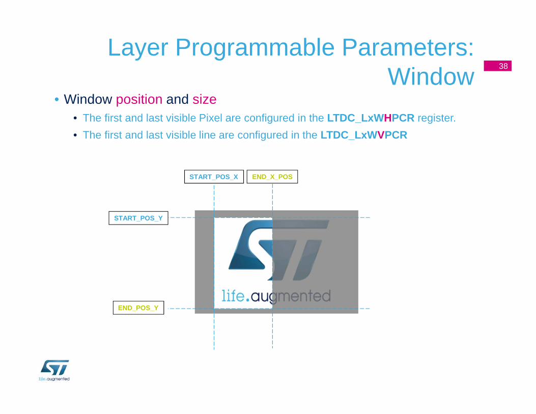
Layer Programmable Parameters: Window
• Window position and size • The first and last visible Pixel are configured in the LTDC_LxW HPCR register.
• The first and last visible line are configured in the LTDC_LxW VPCR
38
START_POS_X
START_POS_Y
END_POS_Y
END_X_POS

Layer Programmable Parameters: Color Frame Buffer
• The frame buffer size, line length and the number of lines settings must be correctly configured :
• If it is set to less bytes than required by the layer, FIFO underrun error will be set.
• If it is set to more bytes than actually required by the layer, the useless data read is discarded. The useless data is not displayed.
39
Line Length
Number of Lines..
Pitch
Frame Buffer
Start of layer frame buffer

Layer Programmable Parameters: Color Frame Buffer - effects
• Simply changing the start of the layer frame buffer you can scroll the picture over the layer
• The picture stored in the memory must be bigger tha n actual layer size
40
.
.
.
.

Demo - Moving layer
• Just by changing the layer buffer address you can move the visible layer over a bitmap which is bigger than the layer.
41
400
320
LTDC_Layer_InitStruct.LTDC_CFBStartAdress = (uint32_t)Image + 3 * (offsetH + (offsetV * Image_width));
• Horizontal scroll
• Vertical scroll• Bytes per pixel
• Base address of image in memory
240
320

Layer Programmable Parameters: Multi-layer blending
• Blending is always active using alpha value
• Blending factors are configured through the LTDC_LxBFCR register• Fixed Constant alpha
• Alpha pixel multiplied by the Constant Alpha
• The blending order is fixed and it is bottom up.
• Programmable Background Color for the bottom layer
42
Layer 2Layer 1
Solid color background
Blending – Example 1
• Layer 1 blending with background• Background is black
• Layer 2 is disabled.
43
75%
25%
0%
50%
100%

Blending – Example 2
• Layer 1 and Layer 2 blending • Background color is black
• Layer 1 Constant Alpha set to 100 %
• Layer 2 Constant Alpha is set to:
44
75 %
25 %
0 %
50 %
100%

Demo – Two Layers
• Example is using two layers• Layer 1 – static background picture
• Layer 2 – moving ST logo with alpha channel
• ST logo is moved using layer 2 parameters only, no load of CPU
• Blending is done directly by Constant Alpha parameter, no load of CPU, done by LTDC controller directly
45

Layer Programmable Parameters: Color Keying
• Transparent color (RGB) can be defined for each layer in the LTDC_LxCKCR register
• When the Color Keying is enabled, the current pixels is compared to the color key. If they match for the programmed RGB value, all channels (ARGB) of that pixel are set to 0.
• Color Keying can be enabled on the fly for each layer in the LTDC_LxCR regiser
46

Demo - Color Keying
• Example is using two layers• Layer 1 – background picture “blue sky”
• Layer 2 – ST logo with white background color
• Keying color is set to WHITE
• Disturbing artifacts can be removed by pre-processing using tools like Photoshop or Gimp, but quality of result is usually depending on the background anyway
• Best suitable for rectangular graphical objects
• Not optimal for photos – use alpha channel blending instead
47
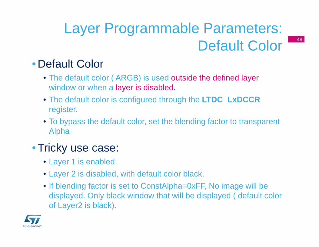
Layer Programmable Parameters: Default Color
• Default Color • The default color ( ARGB) is used outside the defined layer
window or when a layer is disabled.
• The default color is configured through the LTDC_LxDCCRregister.
• To bypass the default color, set the blending factor to transparent Alpha
• Tricky use case: • Layer 1 is enabled
• Layer 2 is disabled, with default color black.
• If blending factor is set to ConstAlpha=0xFF, No image will be displayed. Only black window that will be displayed ( default color of Layer2 is black).
48

LTDC Shadow registers
• The shadowed registers are all the Layer 1 and Layer 2 registers except the CLUT register (LTDC_LxCLUTWR) .
• The shadow registers should not be modified again before the reload has been done.
• The new written value can only be read after the reload has taken place.
• Shadow registers can be reloaded to active registers by:• Immediate Reload
Set IMR bit in LTDC_SRCR register
• Vertical blanking reload
Set VBR bit in LTDC_SRCR register
49
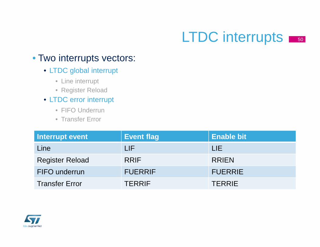
LTDC interrupts• Two interrupts vectors:
• LTDC global interrupt• Line interrupt• Register Reload
• LTDC error interrupt• FIFO Underrun• Transfer Error
50
Interrupt event Event flag Enable bit
Line LIF LIE
Register Reload RRIF RRIEN
FIFO underrun FUERRIF FUERRIE
Transfer Error TERRIF TERRIE

Chrom-ART Accelerator™STM32F4 Graphic Accelerator (DMA2D)
Overview
Font 1
Text 1
Step 2 : Display the frame buffer
• The frame buffer is transferred to the display through a dedicated hardware interface
• Graphical oriented microcontroller are offering a TFTcontroller to drive directly the display
• The frame buffer must be sent at 60fps to have a perfect image color and stability (independently from the animation fps)
Step 1 : Create the content in a frame buffer
• The frame buffer is build by composing graphical primitive• This operation is done by the CPU running a graphical
library software• It can be accelerated by a dedicated hardware used with
the CPU through the graphical library• More often the frame buffer can be updated, more fluent
will be the animations (animation fps)
NextPrev
52
Refresh rate (60 Hz)
Frame rate

Graphical content creation
53

Creating something « cool »
• How the frame buffer is generated for creating a “cool” graphical interface to be displayed through the TFT controller ?
54
-5°C
21°C
62%
Temperature
Humidity
ARMED
14:21

Frame buffer construction
• The frame buffer is generated drawing successively all the graphic objects
55
-5°C
21°C
62%
Temperature
Humidity
ARMED
14:21

Frame buffer generation needs 56
• The resulting frame buffer is an uncompressed bitmap of the size of the screen.
• Each object to be drawn can be• A Bitmap with its own color coding (different from the final one), compressed or not
• A Vector Description (a line, a circle with a texture...etc....)
• (A Text )

Bitmap or Vector 57
Bitmap• High ROM usage• No CPU usage if no compression,
but can be needed for uncompressing
• Geometrical transformations limited and would need filtering
• Description standard bitmap files that are converted into C table
Vector graphics• Low ROM usage• High CPU usage as image needs
to be generated : a GPU is mandatory
• Geometrical transformations are natural
• Description through• Polygons : 3D graphics• Curves : 2D graphics

STM32F42x/F43x Architecture
• TFT controller allows the interfacing • DMA2D provides a true graphical acceleration• DMA2D offloads the CPU for operations like rectangle filling, rectangle
copy (with or without pixel format conversion), and image blending• DMA2D goes faster than the CPU for the equivalent operation
TFTController
InternalFlash
InternalSRAM
ExternalMemory
Controller
Chrom-ART AcceleratorCortex-M4
Bus Matrix
58

Bitmaps
59

Overview
• Bitmap are an array representation of an image
• It shall have the at least following properties• Width (in pixel)
• Height (in pixel)
• Color mode (direct, indirect, ARGB8888, RGB565...etc...)
• Color Look Up Table (optional)
60
Width
Height
How color are coded

Blending
• Blending consist in drawing an image onto another respecting the transparency information
• As a consequence blending implies to read 2 sources, then blend then write to the destination
61
Not Blended
Blended

Back to our « cool » interface 62
-5°C
21°C
62%
Temperature
Humidity
ARMED
14:21Background
Almost UniformL8 mode
Button
Round shapeGradient
ARGB8888 mode
Icon
Complex shapeMany colors
ARGB8888 mode
Fonts
Specific management with A8 or A4 mode

Demo – Content Creation• Moving successively graphical elements from internal FLASH into
the frame buffer by Chrome-ART
63
ARMED
ARMED
DMA2D source parameters:Location in memory, width, height, pixel format
DMA2D destination parameters:Location in buffer, width, height, pixel format, line offset
DMA2D
foreground
background
output
FLASH content

Font management
• Bitmap fonts are managed only using alpha channel (transparency)
64
ROMed character bitmap(A8 or A4)
Generated character bitmapwith color information
(ARGB8888, ARGB1555, ARGB4444)or
(RGB888, RGB565)
PFC
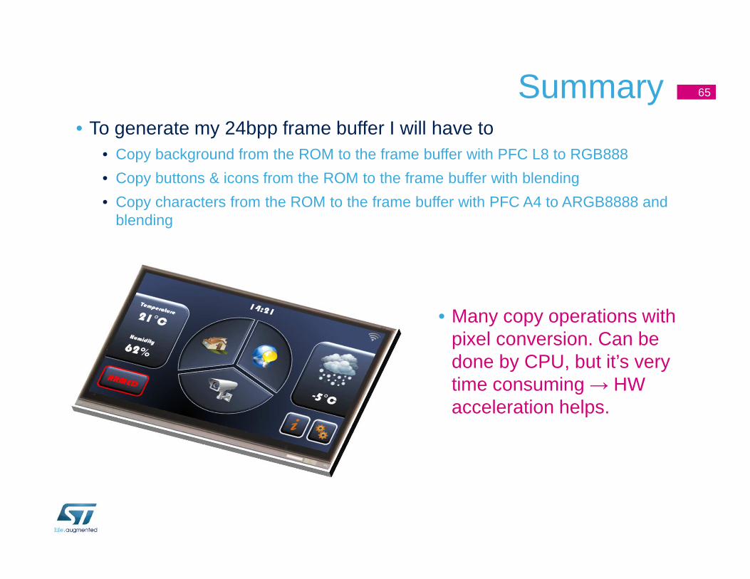
Summary• To generate my 24bpp frame buffer I will have to
• Copy background from the ROM to the frame buffer with PFC L8 to RGB888
• Copy buttons & icons from the ROM to the frame buffer with blending
• Copy characters from the ROM to the frame buffer with PFC A4 to ARGB8888 and blending
65
• Many copy operations with pixel conversion. Can be done by CPU, but it’s very time consuming → HW acceleration helps.

Chrom-ART Accelerator(DMA2D)
66

Overview
• The Chrom-ART combines both a DMA2D and graphical oriented functionality for image blending and pixel format conversion.
• To offload the CPU of raw data copy, the Chrom-ART is able to copy a part of a graphic content into another part of a graphic content, or simply to fill an part of a graphic content with a specified color.
• In addition to raw data copy, additional functionality can be added such as image format conversion or image blending (image mixing with some transparency).
67
TFTController
InternalFlash
InternalSRAM
ExternalMemory
Controller
Chrom-ART AcceleratorCortex-M4
Bus Matrix
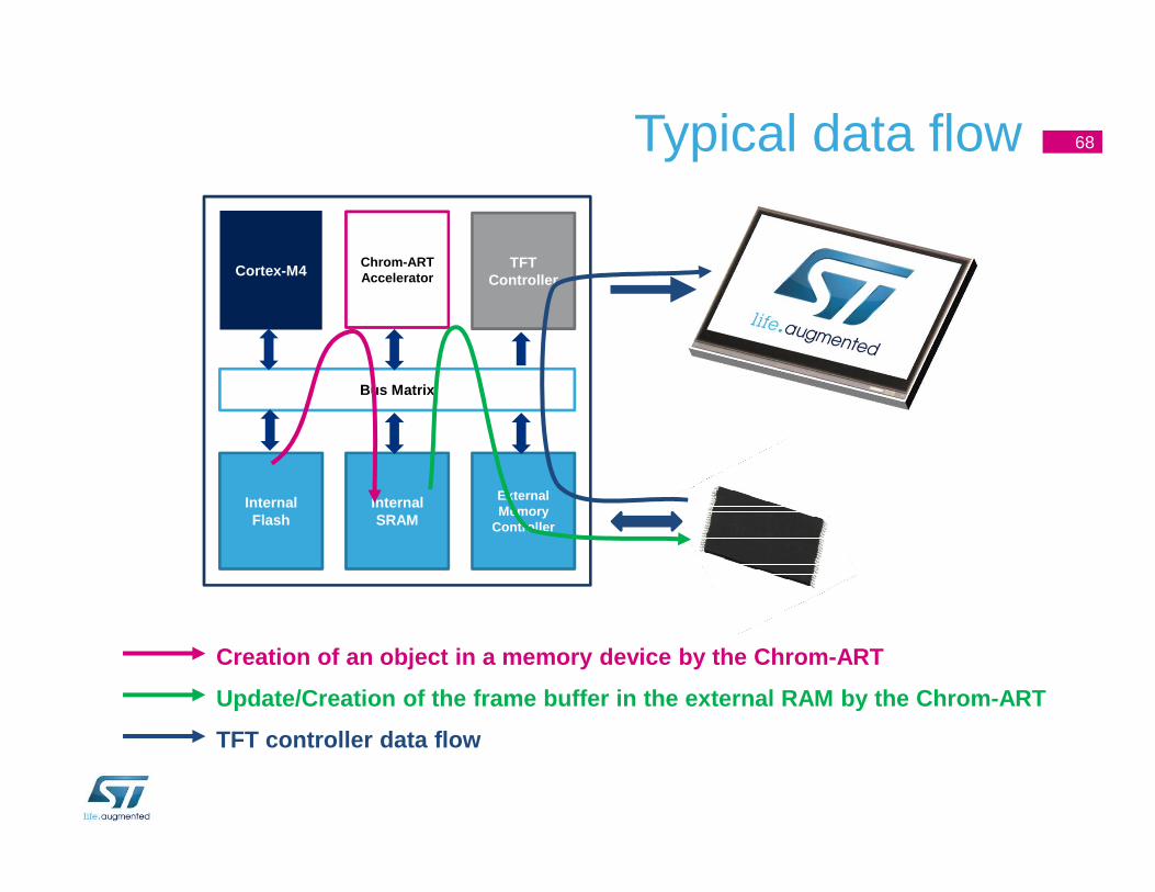
Typical data flow 68
Creation of an object in a memory device by the Chr om-ART
Update/Creation of the frame buffer in the external RAM by the Chrom-ART
TFT controller data flow

Chrom-ART features
• AHB bus master with burst access to any system memory
• Programmable bitmap height, width and address in the memory
• Programmable data format (from 4-bit indirect up to 32-bit direct)
• Dedicated memory for color lookup table (CLUT) independent from LTDC
• Programmable address destination and format
• Optional image format conversion from direct or indirect color mode to direct color mode
• Optional blending machine with programmable transparency factor and/or with native transparency channel between to independent image input to the destination image.
69

Chrom-ART pixel pipeline 70
OutputPFC
BG FIFO
FG FIFO
BG PFC
FG PFC
OutputFIFO
Blender
Foreground
Background

-5°C
21°C
62%
Temperature
Humidity
ARME
D
14:21
Bitmap parameter 71
Width
Height
Original_Width
Original_AddressAddress
Original_Height
Address = Original_Address + (X + Original_Width * Y) * BPPLineOffset = Original_Width - Width

Supported color mode
Color mode Input FG/BG CM[3:0] Output CM[2:0]
ARGB8888 0000 000
RGB888 0001 001
RGB565 0010 010
ARGB1555 0011 011
ARGB4444 0100 100
L8 0101 Not supported
AL44 0110 Not supported
AL88 0111 Not supported
L4 1000 Not supported
A8 1001 Not supported
A4 1010 Not supported
72
CLUT management
• When an indirect color mode L8, AL44 or AL88 is used, the bitmap CLUT must be loaded into the Chrom-ART
• Each FG and BG has its own dedicated memory for CLUT.
• The CLUT can be loaded manually when no Chrom-ART operation are on going
• The CLUT can be loaded automatically configuring the CLUT format (24-bit or 32-bit), the CLUT size and the CLUT address and setting the CLUT Start bit
73
Supported operations
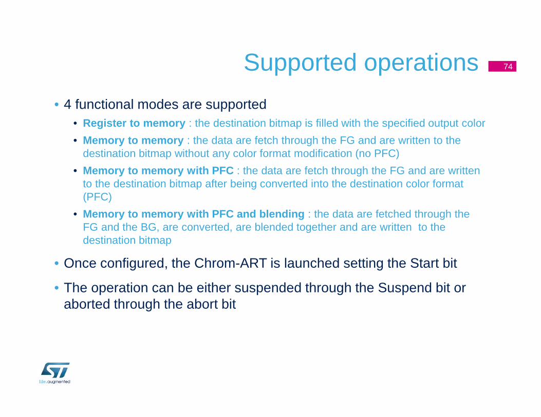
• 4 functional modes are supported• Register to memory : the destination bitmap is filled with the specified output color
• Memory to memory : the data are fetch through the FG and are written to the destination bitmap without any color format modification (no PFC)
• Memory to memory with PFC : the data are fetch through the FG and are written to the destination bitmap after being converted into the destination color format (PFC)
• Memory to memory with PFC and blending : the data are fetched through the FG and the BG, are converted, are blended together and are written to the destination bitmap
• Once configured, the Chrom-ART is launched setting the Start bit
• The operation can be either suspended through the Suspend bit or aborted through the abort bit
74

Alpha modulation• When the PFC is activated the Alpha value of the pixel can be
modified as follow
• Kept as it is
• Replaced by a fixed one
• Replaced by the current one multipliedby the fixed one
• This allows to perform easily fade in/out animations
75
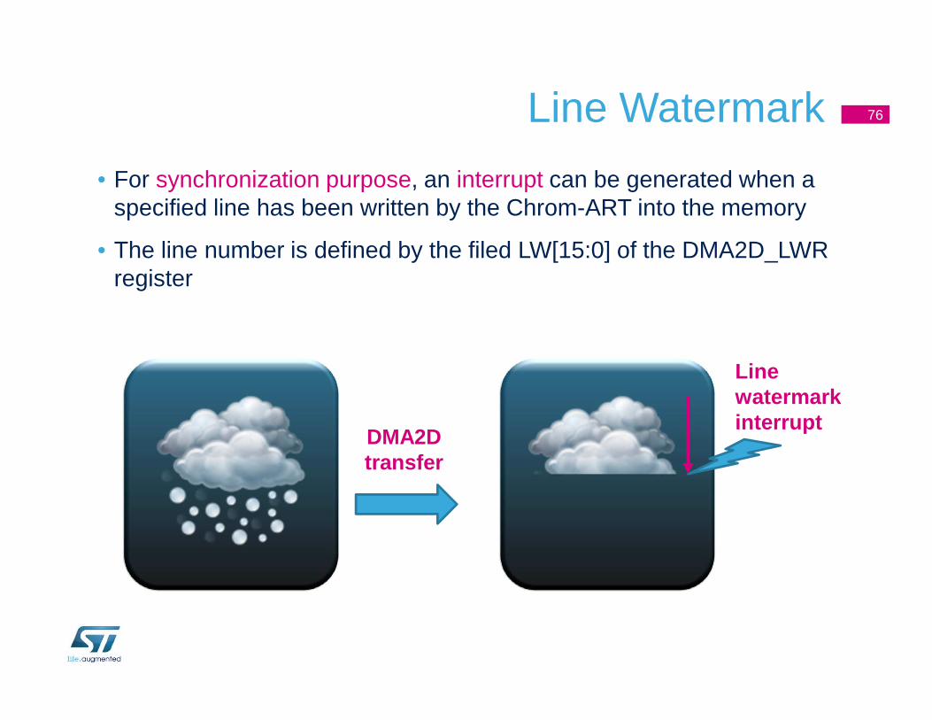
Line Watermark
• For synchronization purpose, an interrupt can be generated when a specified line has been written by the Chrom-ART into the memory
• The line number is defined by the filed LW[15:0] of the DMA2D_LWR register
76
Line watermark interrupt
DMA2D transfer
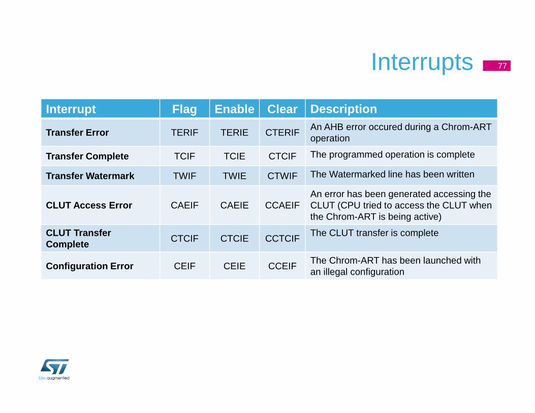
Interrupts
Interrupt Flag Enable Clear Description
Transfer Error TERIF TERIE CTERIFAn AHB error occured during a Chrom-ART operation
Transfer Complete TCIF TCIE CTCIF The programmed operation is complete
Transfer Watermark TWIF TWIE CTWIF The Watermarked line has been written
CLUT Access Error CAEIF CAEIE CCAEIFAn error has been generated accessing the CLUT (CPU tried to access the CLUT whenthe Chrom-ART is being active)
CLUT Transfer Complete
CTCIF CTCIE CCTCIFThe CLUT transfer is complete
Configuration Error CEIF CEIE CCEIFThe Chrom-ART has been launched withan illegal configuration
77

Chrom-ART
Integration with Graphic Library 78
Cortex-M4
STemWin
Application
Cortex-M4
STemWin
Application
• Chrom-ART integration is transparent for the application• The low-level drivers of the graphical stack are upgraded to directly use
Chrom-ART for data transfer, pixel format conversion and blending• CPU load is decreased and graphical operations are faster

STM32 Solution for Graphics
• STM32 offers a unique graphical capability in the Cortex-M based MCU perimeter
• Real TFT Controller for optimum display control
• External memory interface to connect both Flash for static content and SRAM or SDRAM for dynamic content and frame buffer
• On-chip hardware acceleration deeply coupled with graphical library
• Standard graphical library taking advantage of on-chip graphical acceleration
79

Flexible Memory Controller (FMC)
Enhanced and upgrade of FSMC

CONTENTS
• FMC features
• SDRAM protocol
• SDRAM FMC controller
81

OBJECTIVES
• Overview of FMC interface
• Usage of high capacity RAM storage - SDRAM• For frame buffer
• For picture storage and preparation
• For animations
82
82

FMC Features (1/2)
• 6 Banks to support External memories
• FMC external access frequency is up 90MHz when HCLK is at 180MHz
• Independent chip select control for each memory bank
• Independent configuration for each memory bank
• Programmable timings to support a wide range of devices
• 8/16/32 bits data bus
• External asynchronous wait control
• Interfaces with Synchronous DRAM (SDRAM) memory-mapped
83

FMC Features (2/2)
• Interfaces with static memory-mapped devices including:• static random access memory (SRAM)
• read-only memory (ROM)
• NOR/ OneNAND Flash memory
• PSRAM
• Interfaces parallel LCD modules: Intel 8080 and Motorola 6800
• Interfaces with NAND Flash and 16-bit PC Cards• With ECC hardware up to 8 Kbyte for NAND memory
• 3 possible interrupt sources (Level, Rising edge and falling edge)
• Supports burst mode access to synchronous devices (NOR Flash and PSRAM)
84

SDR SDRAM protocol overview
SDRAM memory organization
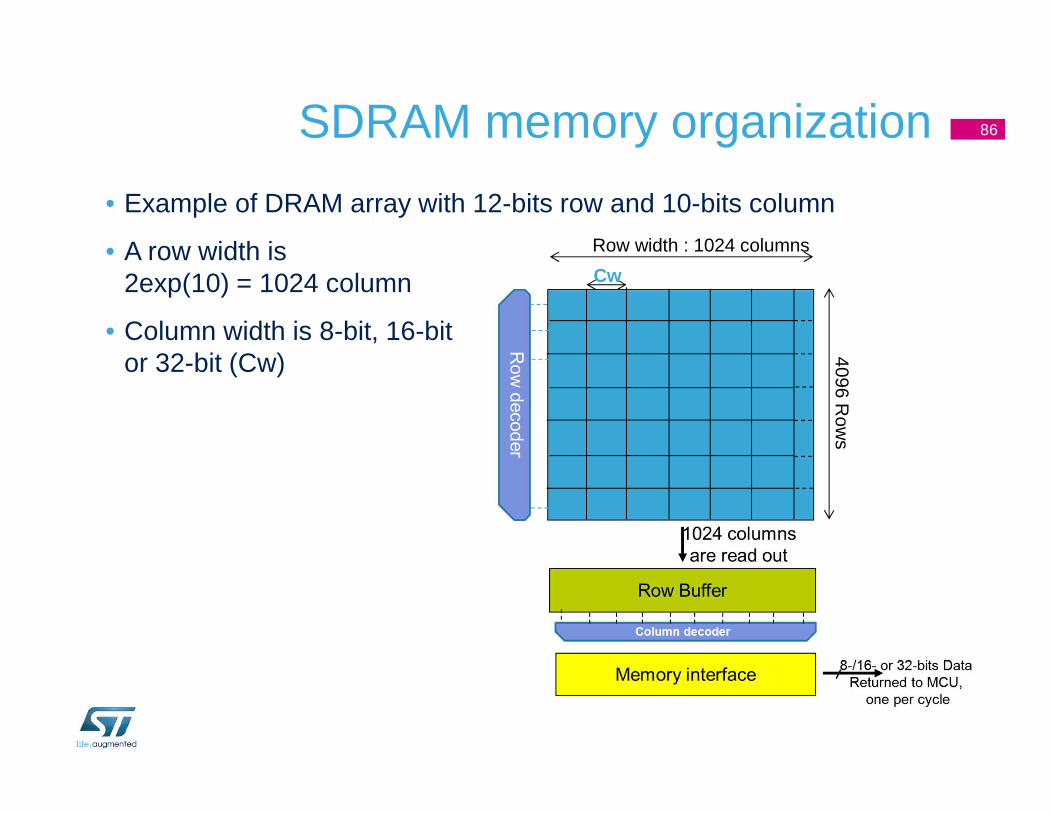
• Example of DRAM array with 12-bits row and 10-bits column
• A row width is 2exp(10) = 1024 column
• Column width is 8-bit, 16-bitor 32-bit (Cw)
Row width : 1024 columns
4096 Row
s
Cw
86

SDRAM memory read operation
• Read operation step 1(*):• On Row Access Strobe (RAS), selected row is copied to “Row Buffer” (a full row is
transferred at once to the Row Buffer)
• Read operation step 2:• On Column Access Strobe (CAS), column is selected from “Row Buffer” and presented on the memory
interface
(*): Row activation is only performed if the row is not active or at a row boundary
87

SDRAM memory read characteristics (1/2)
• SDRAM read characteristics• Reads are destructive: contents are erased after reading
• Row buffer
• read a full row at once (a set of bits all at once), and then break down them based on different column addresses
1
Vdd
Wordline Enabled
Sense Amp Enabled
bitlinevoltage
Vddstorage
cell voltage
sense amp
0
After read cell containssomething close to ½ Vdd
88

SDRAM memory write characteristics
• The SDRAM controller always checks the next write access destination,
• Two cases:• If the next write access is in the same row or in another active row
(in a different bank)• The write operation is carried out
• If the next write access targets another row (not active), the SDRAM controller
• Generates a precharge command• Activates the new row• Initiates a write command

STM32 FMC controller
90

FMC SDRAM main features (1/4)
• Up to 512MB continues memory range split into two banks, can be seen as a single device.
256MB (4x16MBx32-bit)
SDRAM Bank2
256MB (4x16MBx32-bit)
SDRAM Bank1
FMC SDRAM
Up to 512MBIndependent chip select
Independent configurationEasy to use
0xC000 0000
0xDFFF FFFF

SDRAM main features (2/4)
• Fully programmable SDR (single data rate) SDRAM interface
• Configurable SDRAM clock speed• Half AHB speed (HCLK /2),
• One-third AHB speed (HCLK /3)
• Programmable Timing parameters for different SDRAM devices requirements
• Row to column delay ( TRCD )
• Self refresh time
• CAS latency of 1,2,3
• Memory data bus width : 8-bit, 16-bit and 32-bit
• Up to 4 internal banks with configurable Row and Column sizes : • up to 13-bits Address Row,
• up to 11-bits Address Column.

SDRAM main features (3/4)
• Optimized initialization sequence by software• The initialization command sequence are executed simultaneously for the two
banks. Initialization time can be divided by 2.
• Automatic Refresh operation with programmable Refresh rate
• Energy-saving capabilities : two low power modes are supported:• Self-refresh Mode
• Power-down Mode

SDRAM main features (4/4)
• Multibank ping-pong access (FMC SDRAM controller keeps track of the active row in each bank)
• Automatic row and bank boundary management
• Optimized Read access :• Cacheable Read FIFO with depth of 6 lines x 32-bit
• With 6x 14-bit Address Tag to identify each FIFO line content
• Configurable Read Burst (to anticipate next read accesses during CAS latencies)
• Buffered write access• Write Data FIFO with depth of 16
• With 16x Write Address FIFO to identify each FIFO line destination

SDRAM controller benefits
• AHB Slave interface up to 180MHz
• Grant more RAM resources for user application
• Accessible by all AHB masters• CPU can execute code from SDRAM
• Reduce RAM memory cost (SDRAM vs. SRAM)

For more information welcome to visit our website:www.st.com/stm32www.stmcu.com.cn
www.stmcu.org
96

1
使用STM32 设计HMI-软件
介绍使用STM32提供的硬件资源和软件资源开发人机交互界面HMI的方法

Agenda一、STM32 HMI设计硬件资源
LCD controller
ChromeART accelerator
SDRAM interface
二、 STM32 HMI设计软件资源
STemWin
IS2T
TouchGFX
2
12/08/2015
STM32F42xx Technical Training

目录
STM32GUI方案介绍
STM32GUI硬件平台资源评估&选型
STM32GUI软件方案之STemWin
3

过去过去过去过去的嵌入式产品注重用户的实用性的嵌入式产品注重用户的实用性的嵌入式产品注重用户的实用性的嵌入式产品注重用户的实用性4

现在现在现在现在的的的的嵌入式产嵌入式产嵌入式产嵌入式产品更加品更加品更加品更加重重重重视用户体视用户体视用户体视用户体验验验验5

STM32丰富的外设资源和强大的丰富的外设资源和强大的丰富的外设资源和强大的丰富的外设资源和强大的CPU处理能力处理能力处理能力处理能力
为嵌入式为嵌入式为嵌入式为嵌入式GUI系统提供强大的硬件支持系统提供强大的硬件支持系统提供强大的硬件支持系统提供强大的硬件支持
6
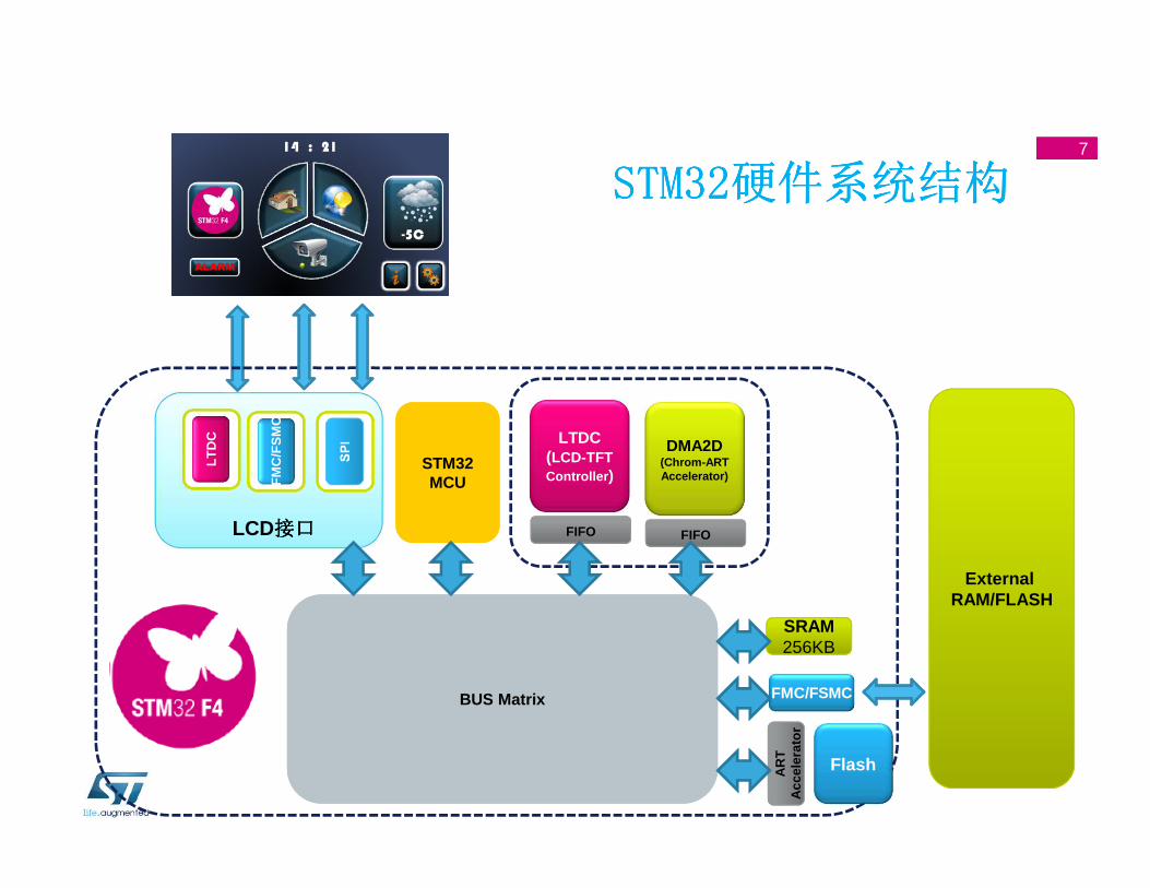
7
STM32STM32STM32STM32硬件系统结构硬件系统结构硬件系统结构硬件系统结构
LTD
C
FM
C/F
SM
C
SRAM256KBSRAM256KB
STM32MCU
STM32MCU
AR
TA
ccel
erat
or
Flash
FMC/FSMC
LTDC(LCD-TFTController )
FIFO
DMA2D(Chrom-ARTAccelerator)
FIFO
ExternalRAM/FLASH
LCD接口接口接口接口
-5C
14
ALARM
: 21
BUS MatrixBUS Matrix

STM32STM32STM32STM32硬件硬件硬件硬件--------LTDCLTDCLTDCLTDC性能演示性能演示性能演示性能演示
((((分辨率分辨率分辨率分辨率1024x768)1024x768)1024x768)1024x768)
LTDC(LCD-TFTController )

STM32STM32STM32STM32硬件硬件硬件硬件--------DMA2DDMA2DDMA2DDMA2D性能演示性能演示性能演示性能演示
DMA2D(Chrom-ARTAccelerator)
DMA2D CPU Load(约约约约)
使用使用使用使用 5%
不使用不使用不使用不使用 95%

10STM32不仅不仅不仅不仅为客户提供丰为客户提供丰为客户提供丰为客户提供丰富富富富的硬件资源的硬件资源的硬件资源的硬件资源
而且为客户提供了而且为客户提供了而且为客户提供了而且为客户提供了STM32 GUI软件开发平台软件开发平台软件开发平台软件开发平台
TouchGFX
IS2T
STemWin

11STM32GUI软件开发平台软件开发平台软件开发平台软件开发平台--STemWin
12STM32GUI软件开发平台软件开发平台软件开发平台软件开发平台--STemWin
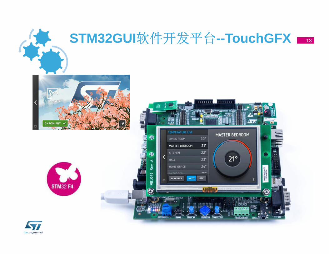
13STM32GUI软件开发平台软件开发平台软件开发平台软件开发平台--TouchGFX
14STM32GUI软件开发平台软件开发平台软件开发平台软件开发平台--TouchGFX

15STM32GUI软件开发平台软件开发平台软件开发平台软件开发平台—IS2T

16STM32GUI软件开发平台软件开发平台软件开发平台软件开发平台—IS2T

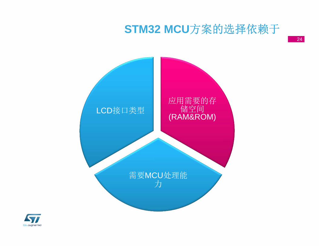
STM32GUI硬硬硬硬件平台件平台件平台件平台资资资资源评估源评估源评估源评估&选型选型选型选型
17
18
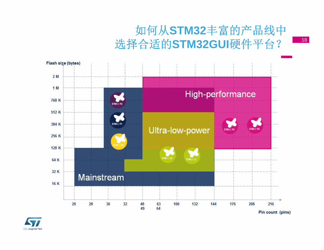
如何从如何从如何从如何从STM32丰富的产品线中丰富的产品线中丰富的产品线中丰富的产品线中
选择合适的选择合适的选择合适的选择合适的STM32GUI硬件平台硬件平台硬件平台硬件平台????

19
应用需要的存
储空间
(RAM&ROM)
需要MCU处理能
力
LCD接口类型
STM32 MCU方方方方案的选择需考虑案的选择需考虑案的选择需考虑案的选择需考虑

20
应用需要的存
储空间
(RAM&ROM)
需要MCU处理能
力
LCD接口类型
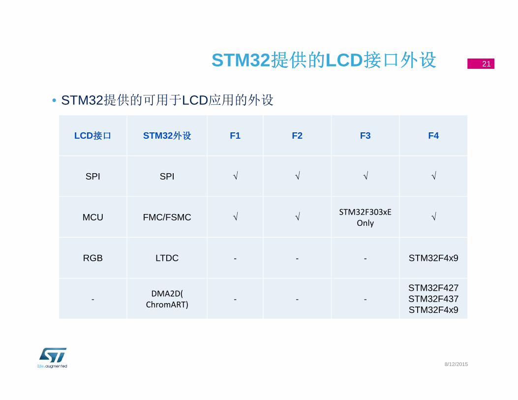
STM32提供的提供的提供的提供的LCD接口外设接口外设接口外设接口外设
• STM32提供的可用于LCD应用的外设
8/12/2015
21
LCD接口接口接口接口 STM32外外外外设设设设 F1 F2 F3 F4
SPI SPI √ √ √ √
MCU FMC/FSMC √ √STM32F303xE
Only√
RGB LTDC - - - STM32F4x9
-DMA2D(
ChromART)- - -
STM32F427STM32F437STM32F4x9

主主主主流流流流LCD接口接口接口接口
• SPI• 写屏速度较慢
• 接口简单
• 不需要独立显存
8/12/2015
22
FMC/FSMC(8080/6800)
写屏速度较快
接口较复杂
不需要独立显存

主流主流主流主流LCD接口接口接口接口((((续续续续))))
• LTDC(RGB)• 写屏速度较快
• 写屏不需要CPU干预
• 接口较复杂
• 需要MCU提供显存
• 只有STM32F429提供LTDC外设
8/12/2015
23
LCD_G[7:0]
LCD_B[7:0 ]
LCD_CLK
LCD_HSYNC
LCD_VSYNC
LCD_DE
LCD_R[7:0 ]
LCD PanelSTM32F429
24
应用需要的存
储空间
(RAM&ROM)
需要MCU处理能
力
LCD接口类型
STM32 MCU方方方方案的选择依赖于案的选择依赖于案的选择依赖于案的选择依赖于

ROM和和和和RAM(以以以以STemWin为例为例为例为例)
• 对存储空间(ROM/RAM)的
需求
• 应用程序的最小需求(STemWin)• 在不使用窗口管理时
• ROM 8.1KB• RAM 334Byte
• 在使用窗口管理时
• ROM 60KB• RAM 6.6Byt
• 随着用户界面的复杂程度增加,对应
的ROM和RAM的需求会随之增加。
• 可以使用外扩RAM作为STemWin的内存
8/12/2015
25

• 内存分配
• 可以灵活选择
MCU内部SRAM或者外部RAM作为STemWin的内存块
26内存分配(以STemWin为例)
SPIFSMCLTDC
((((DMA))))
InternalFlash
InternalSRAM
ExternalMemory
Controller
CPU
Bus Matrix
内部内部内部内部RAM作作作作为为为为内存空内存空内存空内存空间间间间
外部外部外部外部RAM作作作作为为为为内存空内存空内存空内存空间间间间

27
应用需要的存
储空间
(RAM&ROM)
MCU处理能力
LCD接口类型
STM32 MCU方方方方案的选择依赖于案的选择依赖于案的选择依赖于案的选择依赖于

• 市面上的主流LCD液晶屏接口及对比
8/12/2015
28
LCD接口接口接口接口 数据内存数据内存数据内存数据内存 显示内存显示内存显示内存显示内存 CPU任务任务任务任务 DMA参与传送参与传送参与传送参与传送
SPI MCU/扩展内存 LCD控制器内置 构图+传输 √
FMC/FSMC
(8080/6800)MCU/扩展内存 LCD控制器内置 构图+传输 √
LTDC(RGB)
MCU/扩展内存
MCU片内SRAM
或
扩展SDRAM
构图
(STM32F4x9)DMA2D

29
应用需要的存
储空间
(RAM&ROM)
需要MCU处理能
力
LCD接口类型
STM32 MCU方方方方案的选择依赖于案的选择依赖于案的选择依赖于案的选择依赖于
•根据应用进行MCU选择
• 需要的CPU速度
• 72MHz ~ 180MHz
• 接口
• SPI,8080/6800,RGB
• RAM/ROM用量
• 确定需要的MCU的Flash/SRAM size
• 需要外扩RAM作为数据内存或者显存,外扩RAM的类型
• 确定是否需要FSMC(SRAM/PSRAM),FMC(SDRAM)

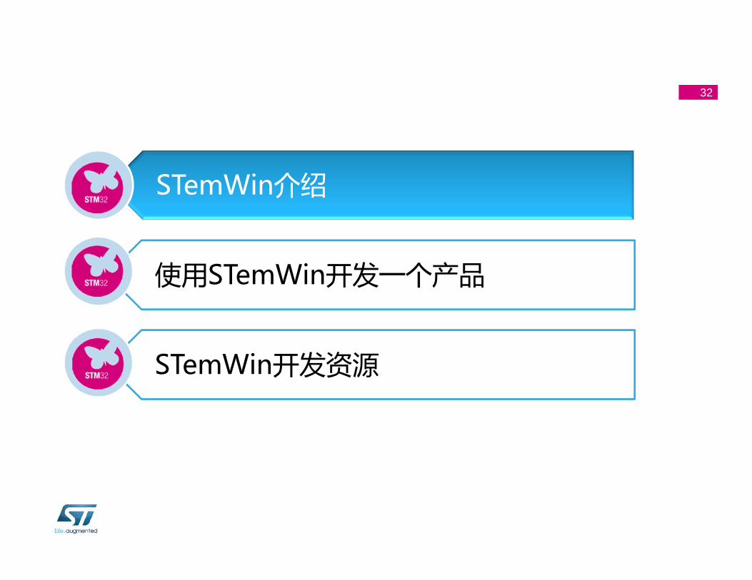
STM32GUI软件方案之软件方案之软件方案之软件方案之STemWin
30

31
STemWin介绍
使用STemWin开发一个产品
STemWin开发资源
预览
32
STemWin介绍
使用STemWin开发一个产品
STemWin开发资源

STemWinSTemWinSTemWinSTemWin是什么是什么是什么是什么
�ST和Segger公司联合提供的嵌入式GUI方案
33
12/08/2015Presentation Title
STM32
emWin
STemWin
�STemWin高度可裁剪可移植性,完全支持STM32全系列MCU
STemWinSTemWinSTemWinSTemWin特性特性特性特性
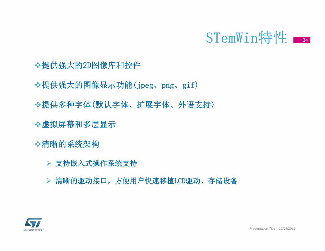
�提提提提供强大的供强大的供强大的供强大的2D2D2D2D图像库和控件图像库和控件图像库和控件图像库和控件
�提提提提供强大的图像显示功能供强大的图像显示功能供强大的图像显示功能供强大的图像显示功能(jpeg(jpeg(jpeg(jpeg、、、、pngpngpngpng、、、、gif)gif)gif)gif)
�提提提提供多种字体供多种字体供多种字体供多种字体((((默默默默认字体认字体认字体认字体、、、、扩展字体扩展字体扩展字体扩展字体、、、、外语支持外语支持外语支持外语支持))))
�虚拟屏幕和虚拟屏幕和虚拟屏幕和虚拟屏幕和多层显多层显多层显多层显示示示示
�清晰的系统架构清晰的系统架构清晰的系统架构清晰的系统架构
� 支持嵌入式操作系统支持支持嵌入式操作系统支持支持嵌入式操作系统支持支持嵌入式操作系统支持
� 清晰的驱动接口清晰的驱动接口清晰的驱动接口清晰的驱动接口,,,,方便用户快速移植方便用户快速移植方便用户快速移植方便用户快速移植LCDLCDLCDLCD驱动驱动驱动驱动、、、、存储设备存储设备存储设备存储设备
34
12/08/2015Presentation Title

STemWinSTemWinSTemWinSTemWin提供丰富美观的提供丰富美观的提供丰富美观的提供丰富美观的GUIGUIGUIGUI控件控件控件控件
12/08/2015
35

36
STemWin介绍
使用STemWin开发一个产品
STemWin开发资源

-5C
14 : 21
ALARM
37
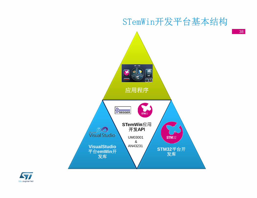
应用程序应用程序应用程序应用程序
VisualStudio平台平台平台平台emWin开开开开
发库发库发库发库
STemWin应用应用应用应用
开发开发开发开发API
STM32平台开平台开平台开平台开
发库发库发库发库
STemWinSTemWinSTemWinSTemWin开发平台基本结构开发平台基本结构开发平台基本结构开发平台基本结构
UM03001&
AN43231
38

资源准备
•准备资源准备资源准备资源准备资源
•图片图片图片图片////字体字体字体字体////控件控件控件控件////动画等资源文件动画等资源文件动画等资源文件动画等资源文件
•代码转换代码转换代码转换代码转换
•将资源文件转换为代码或者存储在外部存储器将资源文件转换为代码或者存储在外部存储器将资源文件转换为代码或者存储在外部存储器将资源文件转换为代码或者存储在外部存储器
VisualStudio平台
开发应用程序
• 基于基于基于基于VS平台开发包和平台开发包和平台开发包和平台开发包和STemWin GUI API 开发应用程序开发应用程序开发应用程序开发应用程序
• 在在在在VS调试仿真工具调试效果调试仿真工具调试效果调试仿真工具调试效果调试仿真工具调试效果
STM32开发平台
移植
• 基于基于基于基于STM32 STemWin库进行移植库进行移植库进行移植库进行移植
• STM32平台选择平台选择平台选择平台选择
• STM32 MCU BSP移植移植移植移植
• 应用代码移植应用代码移植应用代码移植应用代码移植
• 调试运行调试运行调试运行调试运行
• 软件版本发布软件版本发布软件版本发布软件版本发布
STemWinSTemWinSTemWinSTemWin开发平台基本结构和开发方法开发平台基本结构和开发方法开发平台基本结构和开发方法开发平台基本结构和开发方法
39
2.1. 资源准备资源准备资源准备资源准备
40

2.1 2.1 2.1 2.1 资源准备资源准备资源准备资源准备————图片资源处理图片资源处理图片资源处理图片资源处理
12/08/2015
�使用BitmapConverter软件将bmp图片资源生成相应的.c文件
41
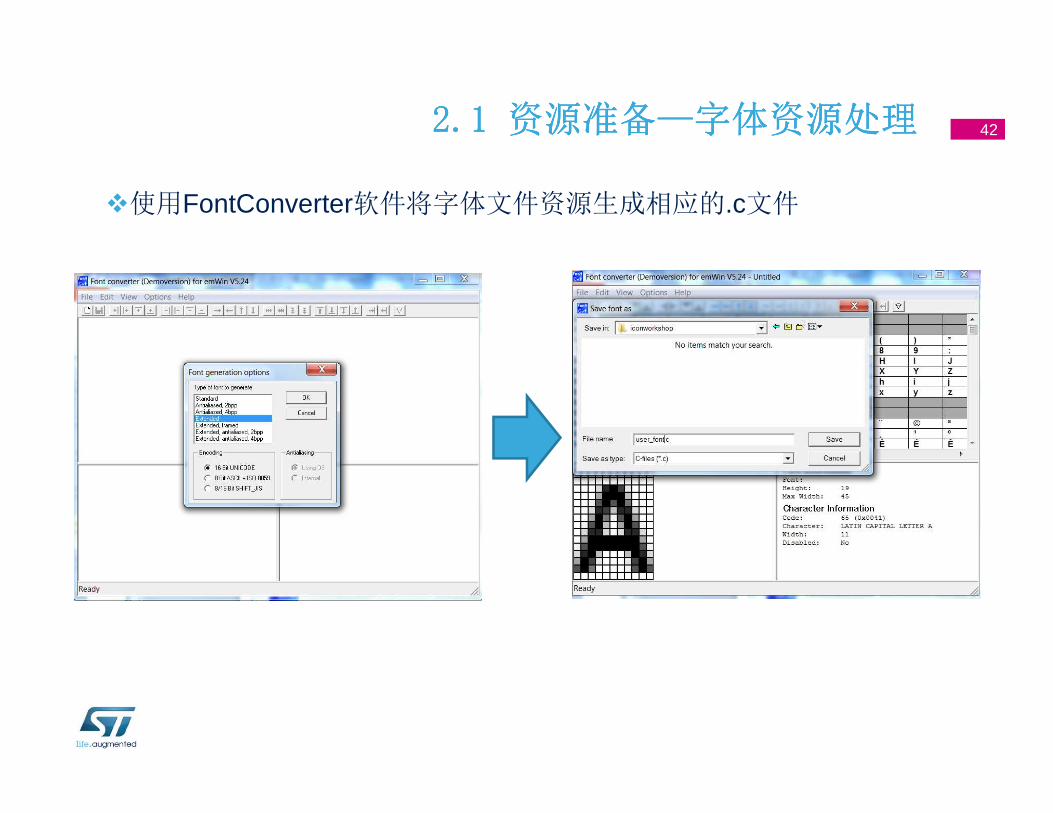
2.1 2.1 2.1 2.1 资源准备资源准备资源准备资源准备————字体资源处理字体资源处理字体资源处理字体资源处理
�使用FontConverter软件将字体文件资源生成相应的.c文件
42
2.1 2.1 2.1 2.1 资源准备资源准备资源准备资源准备————控件资源处理控件资源处理控件资源处理控件资源处理
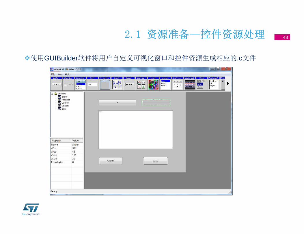
�使用GUIBuilder软件将用户自定义可视化窗口和控件资源生成相应的.c文件
43

2.2 使使使使用用用用VSVSVSVS开发应用程序开发应用程序开发应用程序开发应用程序
44

2.2 2.2 2.2 2.2 使使使使用用用用VSVSVSVS开发应用程序开发应用程序开发应用程序开发应用程序----认识认识认识认识STemWinVSSTemWinVSSTemWinVSSTemWinVS开发环境开发环境开发环境开发环境
12/08/2015
45
图标转换的C资源文件
主程序
主程序入口
绘制背景
绘制Layer0绘制Layer1

2.2 2.2 2.2 2.2 使使使使用用用用VSVSVSVS开发应用程序开发应用程序开发应用程序开发应用程序----绘制背景层绘制背景层绘制背景层绘制背景层
static void background_deal(void){
GUI_DrawBitmap(&bmbg_big, 0,0);
}
46

2.2 2.2 2.2 2.2 使使使使用用用用VSVSVSVS开发应用程序开发应用程序开发应用程序开发应用程序----绘制绘制绘制绘制layer0layer0layer0layer0层层层层
static void layer0_deal(void){
int i = 0;
for(i=0;i<GUI_COUNTOF(_aBitmapItem_layer0);i++){
GUI_DrawBitmap(_aBitmapItem_layer0[i].pBitmap, _aBitmapItem_layer0[i].x,_aBitmapItem_layer0[i].y);
}}
47

2.2 2.2 2.2 2.2 使使使使用用用用VSVSVSVS开发应用程序开发应用程序开发应用程序开发应用程序----绘制绘制绘制绘制layer1layer1layer1layer1层层层层
static void layer1_deal(void){
int i = 0;GUI_SelectLayer(1);GUI_SetColor(GUI_TRANSPARENT);for(i=0;i<GUI_COUNTOF(_aBitmapItem_layer1);i++){
GUI_DrawBitmap(_aBitmapItem_layer1[i].pBitmap, _aBitmapItem_layer1[i].x,_aBitmapItem_layer1[i].y);
}}
48

12/08/2015
2.2 2.2 2.2 2.2 使用使用使用使用VSVSVSVS开发应用程序开发应用程序开发应用程序开发应用程序----VSVSVSVS调试工具运行调试工具运行调试工具运行调试工具运行 49

2.3 应用程序移植到应用程序移植到应用程序移植到应用程序移植到STM32
50

2.3 应用程序移植到应用程序移植到应用程序移植到应用程序移植到STM32
12/08/2015
� 应用代码移植
�STM32 MCU BSP移植
51

将应用程序移植将应用程序移植将应用程序移植将应用程序移植STM32 MCU开发平台开发平台开发平台开发平台
12/08/2015
应应应应用代码移植用代码移植用代码移植用代码移植
52

• 信息收集
• 目标平台的LCD控制器
• 了解目标平台的LCD类型
• 目标平台的内存配置
• 要用到的ROM/RAM大小,决定是否移植,部分移植还是全部移植
• 能否使用外扩RAM
• 目标平台的输入设备
• 了解目标平台的输入设备
• 触摸
• 鼠标
STM32 MCU BSP移植
53

54
STemWin的驱动设置
- 从GUI_Init()开始
将预先定义好的内存块的地址传给STemWin并由其管理这块内存。这个内存块通常是一个
数组或者是一片连续的内存空间
这个内存块可以位于STM32的片上SRAM,
也可以位于外扩的SDRAM
STemWin集成了很多LCD控制器,要根据所使
用的LCD控制器进行驱动选择
设定应用需要的虚拟屏幕的分辨率,虚拟屏幕
的分辨率可以不同于LCD屏的物理分辨率
设定LCD屏的物理分辨率
设定MCU提供的显存入口地址,如果显存在
LCD上则不需要设定
触摸设备校准及方向设置,可以在STemWin中填写,也可以在BSP中完成
显示驱动回调函数,一个任务是使显示开始工
作,其他要求执行硬件相关的操作如开显示启,
关闭显示,设定显示位置等。如果LCD不支持
这些操作,则不用处理这些操作。
应用程序只需要调用GUI_Init()初始化

12/08/2015
调调调调试运试运试运试运行行行行 55

56
STemWin介绍
使用STemWin开发一个产品
STemWin开发资源

开开开开发资源获取发资源获取发资源获取发资源获取
12/08/2015
• PC端端端端开开开开发工具集发工具集发工具集发工具集
• VisualStudio2010
• SeggerEval_WIN32_MSVC_MinGW_GUI_V52 4
• STM32开发工具集开发工具集开发工具集开发工具集
• IAR/KEIL
• STemWin 例程例程例程例程库库库库((((Tools 目录下包含了一些小工具目录下包含了一些小工具目录下包含了一些小工具目录下包含了一些小工具))))
http://www.st.com/web/catalog/tools/FM147/CL1794/SC 961/SS1743/LN1734/PF259225
• 文档资源文档资源文档资源文档资源
• STemWin 例程库例程库例程库例程库((((Documents 目目目目录录录录下下下下))))
• 图图图图像处理软件像处理软件像处理软件像处理软件(举例举例举例举例)• GIMP(图像处理软件图像处理软件图像处理软件图像处理软件)
• IconWorkshop( 图标处理工具图标处理工具图标处理工具图标处理工具)
57

更多资料敬请访问ST官方网站
www.st.com/stm32www.stmcu.com.cn
www.stmcu.org
58