01528608_pwm of zsource
DESCRIPTION
Pulse-Width Modulation of Z-Source InvertersTRANSCRIPT

1346 IEEE TRANSACTIONS ON POWER ELECTRONICS, VOL. 20, NO. 6, NOVEMBER 2005
Pulse-Width Modulation of Z-Source InvertersPoh Chiang Loh, Member, IEEE, D. Mahinda Vilathgamuwa, Senior Member, IEEE, Yue Sen Lai, Geok Tin Chua,
and Yunwei Li, Student Member, IEEE
Abstract— -Source inverters have recently been proposedas an alternative power conversion concept as they have bothvoltage buck and boost capabilities. These inverters use a uniqueimpedance network, coupled between the power source and con-verter circuit, to provide both voltage buck and boost properties,which cannot be achieved with conventional voltage-source andcurrent-source inverters. To facilitate understanding of -sourceinverter modulation, this paper presents a detailed analysis,showing how various conventional pulse-width modulation strate-gies can be modified to switch a voltage-type -source invertereither continuously or discontinuously, while retaining all theunique harmonic performance features of these conventionalmodulation strategies. This paper starts by analyzing the modu-lation requirements of a single-phase H-bridge -source inverter,and subsequently extends the analysis to cover the more complexthree-phase-leg and four-phase-leg -source inverters, with car-rier-based implementation reference equations derived for all theinverters. The theoretical and modulation concepts presented havebeen verified both in simulation and experimentally.
Index Terms—Buck-boost, current source inverters (CSIs),pulse-width modulation (PWM), voltage source inverters (VSIs),
-source inverters.
I. INTRODUCTION
TRADITIONALLY, power inverters can be broadly clas-sified as either the voltage-source inverter (VSI) or cur-
rent-source inverter (CSI) type, as shown in Fig. 1. For a VSI,the inverter is fed from a dc voltage source usually with a rela-tively large capacitor connected in parallel, as in Fig. 1(a). It iswell known that the maximum ac voltage output of a VSI is lim-ited to 1.15 times half the dc source voltage (using modulationstrategies with triplen offsets added) before being over-modu-lated. The VSI can therefore only be used for buck (step-down)dc–ac power conversion or boost (step-up) ac–dc power recti-fication, assuming that no additional dc–dc converter is usedto buck/boost the dc link voltage. On the other hand, a CSI isfed from a dc current source, which is usually implemented byconnecting a dc source in series with a relatively large inductoras in Fig. 1(b), and its ac voltage output is always greater thanthe dc source voltage that feeds the dc-side inductor. The CSIis therefore only suitable for boost dc–ac power conversion orbuck ac–dc power rectification.
Manuscript received June 17, 2004; revised February 25, 2005. This paperwas presented at the 39th IEEE IAS Annual Meeting Conference, Seattle, WA,October 3–7, 2004. Recommended by Associate Editor P. M. Barbosa.
P. C. Loh, D. M. Vilathgamuwa, and Y. Li are with the Center for AdvancedPower Electronics, School of Electrical and Electronic Engineering, NanyangTechnological University, Singapore S639798 (e-mail: [email protected];[email protected]; [email protected]).
Y. S. Lai is with A Lighting Enterprise, Singapore 389422 (e-mail:[email protected]).
G. T. Chua is with the Economic and Development Board (Singapore) Attach-ment Program, Kanagawa 212-8520, Japan (e-mail: [email protected]).
Digital Object Identifier 10.1109/TPEL.2005.857543
Fig. 1. Typical dc–ac inverter topologies (a) VSI and (b) CSI.
For applications requiring both buck and boost power con-versions, -source inverters have recently been proposed as apossible solution with many performance benefits summarizedin [1]. Fig. 2(a) shows the general representation of a -sourceinverter, where a unique impedance network is coupled betweena power source and an inverter circuit. The power source andinverter circuit can be of either the voltage-source or current-source type, and the impedance network is implemented usinga split-inductor ( and ) and capacitors ( and ) con-nected in shape. This unique impedance network allows the
-source inverter to buck and boost its output voltage, and alsoprovides it with unique features that cannot be achieved withconventional VSIs and CSIs [1].
Given its many benefits, this paper now presents a detailedanalysis on the modulation of voltage-type -source inverters(see Fig. 2). This paper shows how various conventionalVSI pulse-width modulation (PWM) strategies (e.g., centeredspace vector modulation (SVM) and 60 -discontinuous PWM[2]–[5]) can be modified to switch a -source inverter either
0885-8993/$20.00 © 2005 IEEE

LOH et al.: PULSE-WIDTH MODULATION OF -SOURCE INVERTERS 1347
Fig. 2. Z-source inverter (a) general representation and (b) voltage-typeconfiguration with N phase-legs.
continuously or discontinuously, while retaining all the uniqueharmonic performance features of these conventional PWMstrategies. First, this paper starts by analyzing the modulationrequirements of a single-phase H-bridge -source inverter, andsubsequently extends the analysis to cover the more complexthree-phase-leg and four-phase-leg -source inverters, withcarrier-based implementation reference equations derived forall the presented inverters. The theoretical and modulationconcepts presented in the paper have been verified by bothdetailed MATLAB simulation and experimental investigations.
II. OPERATIONAL PRINCIPLES OF VOLTAGE-TYPE
-SOURCE INVERTER
Fig. 2(b) shows the topology of a voltage-type -source in-verter with phase-legs ( 2 for H-bridge, 3 forthree-phase-leg, and 4 for four-phase-leg inverters), wherea dc voltage source and a conventional voltage-source converterwith two, three, or four phase-legs, are connected at oppositeends of the -source impedance network. (Note that an optionaldiode can be connected in series with the power source to blockthe reverse flow of current, if required.) Voltage-type -sourceinverters are considered here because voltage-type inverters aregenerally more established and can conveniently be constructedusing low-cost, high-performance insulated gate bipolar tran-sistor (IGBT) modules (with integrated anti-parallel diode) orintelligent power modules.
With the use of the same topology as that of a conventionalVSI, a voltage-type -source inverter can assume all active (fi-nite output voltage) and null (0 V output voltage) switchingstates of VSI. But unlike the conventional VSI where dead-timedelays are inserted to the complementary switching of the twoswitches of a phase-leg to prevent short-circuiting of the phase-leg, a voltage-type -source inverter has the unique feature ofallowing both power switches of a phase-leg to be turned ON
simultaneously (shoot-through state) without damaging the in-verter [1]. The impact of this phase-leg shoot-through on the
Fig. 3. Z-source inverter equivalent circuits when in (a) shoot-through stateand (b) nonshoot-through state.
inverter performance can be analyzed by considering the equiv-alent circuits shown in Fig. 3. When in a shoot-through stateduring time interval , the inverter side of the -source net-work is shorted as in Fig. 3(a). Therefore, (assuming
and )
(1)
Alternatively, when in a nonshoot-through active or null stateduring time interval , current flows from the -source net-work through the inverter topology to the connected ac load. Theinverter side of the -source network can now be represented byan equivalent current source, as shown in Fig. 3(b). This currentsource sinks a finite current when in a nonshoot-through activestate and sinks zero current when in a nonshoot-through nullstate. From Fig. 3(b), the following equations can be written:
(2)
Averaging the voltage across a -source inductor over aswitching period ( 0, where ) then gives
(3)
Using (2) and (3), the peak dc voltage V across the inverterphase-legs and the peak ac output voltage V can be written as
V (4)
VV
(5)
where is the boost factor introduced by the shoot-throughstate, is the modulation ratio commonly used for con-ventional VSI modulation, and the term in {} gives the ac

1348 IEEE TRANSACTIONS ON POWER ELECTRONICS, VOL. 20, NO. 6, NOVEMBER 2005
TABLE ISWITCHING STATES OF H-BRIDGE Z-SOURCE INVERTER (!S REPRESENTS
COMPLEMENT OF S , WHERE X = 1 OR 3)
output of a conventional VSI. Obviously, (5) shows that the acoutput voltage of a -source inverter is boosted by a factor of
always 1 , which cannot be achieved with a conventionalVSI (assuming no additional dc–dc converter is used).
III. MODULATION OF SINGLE-PHASE H-BRIDGE
-SOURCE INVERTER
As described in Section II, the unique feature ofa voltage-type -source inverter is that it allows theshooting-through of an inverter phase-leg, which in turngives rise to an ac output voltage boost, controlled by varyingthe duty cycle . This section now presents an analysis onhow to introduce phase-leg shoot-through appropriately to themodulation of a simple H-bridge -source inverter. Extensionsof the concepts to cover more complex three-phase-leg andfour-phase-leg inverters are presented in the next two sections.
A. Switching State Sequence and Placement
Consider a topology with 2 in Fig. 2(b), the sevenswitching states of a single-phase -source inverter are listedin Table I. The active and null states in which the two switchesof a phase-leg are switched complementary, are commonto both conventional VSI and H-bridge -source inverter.However, the remaining three shoot-through states in whichone (shoot-through states H1 and H2) or two phase-legs(shoot-through state H3) are short-circuited, are unique to theH-bridge -source inverter. Also, observe from Section IIand Table I that when in a shoot-through state, the dc linkcapacitor voltages are boosted but the inverter output voltage iskept at 0 V, similar to that of a null state where the ac load isshort-circuited. Therefore, for a fixed switching cycle, insertingof shoot-through states within the null intervals with the activestate intervals maintained constant will not alter the normalized(relative to ) volt–sec average per switching cycle. This fea-ture allows all existing volt–sec PWM methods to be used forcontrolling a -source inverter with only minor modificationsadded to insert the shoot-through states.
As an illustration, Fig. 4 shows the PWM switchingof a conventional single-phase VSI and a single-phase
-source inverter. For conventional VSI modulation,two state transitions occur per switching cycle (e.g.,null active null ) with the active statecentrally placed within the switching period to minimize thegenerated harmonic distortion [2]. For -source inverter modu-lation, additional shoot-through states are carefully added to thenull intervals with the active interval kept constant and centrally
Fig. 4. Modulation of single-phase Z-source inverter.
placed within the switching period to retain all the harmonicbenefits of central active state placement. The shoot-throughstates should preferably have the same time interval to mini-mize the size of the dc network inductors [1], and should beadded immediately adjacent to the instants of state transitionsof a conventional VSI to ensure a single device switching perstate transition. Therefore, for a single-phase -source inverterwith two state transitions per switching cycle, the number ofequal-interval ( 2) shoot-through states that can be insertedis two. Their inclusions are shown in Fig. 4. In addition, notethat only shoot-through states H1 and H2 can be used in thepreferred state sequence since shoot-through state H3 cannot bereached from any nonshoot-through (active or null) state withonly a single device switching.
B. Carrier-Based Implementation
For synthesizing the preferred state sequence in Fig. 4through carrier-based implementation, this subsection explains,with reference to the reference/carrier comparison diagramsin Fig. 4, the formulation of modulating references neededfor carrier-based -source inverter modulation. For a conven-tional VSI, the reference signals used arefor modulating phase-leg , and for phase-leg
. In general, the first state transition during the fallingcarrier edge occurs when the maximum of the two signals
( in Fig. 4) crosses the fallingslope of the carrier at time . To insert a shoot-through state

LOH et al.: PULSE-WIDTH MODULATION OF -SOURCE INVERTERS 1349
adjacent to this transition from to , the upper(odd-numbered) and lower (even-numbered) switches of therelevant -source phase-leg should therefore be modulatedusing (normalized with respect to )
(6)
or
where ( in Fig. 4) causes the upper switchto turn ON at and ( in Fig. 4)causes the lower switch to turn OFF at . Obviously, theseswitching actions insert the desired shoot-through state H1, asillustrated in the lower half of Fig. 4.
Following through similar analysis, the second shoot-throughstate H2 can be inserted from to by using thefollowing modified reference signals for controlling the othertwo switches
(7)
or
where represents the minimumof and ( , ,
in Fig. 4). Without modification, thesame derived equations (6) and (7) can also be used for en-suring the correct insertion of shoot-through states during therising carrier edge.
IV. MODULATION OF THREE-PHASE-LEG -SOURCE INVERTER
For a three-phase-leg VSI, both continuous switching (e.g.,centered SVM) and discontinuous switching (e.g., 60 -discon-tinuous PWM) are possible with each having its own unique nullplacement at the start and end of a switching cycle and charac-teristic harmonic spectrum. This section now extends the anal-ysis presented in Section III to derive various continuous anddiscontinuous PWM strategies for a three-phase-leg -sourceinverter (see Fig. 2(b) with 3) with each having the samecharacteristic spectrum as its conventional counterpart.
A. Continuous PWM—State Sequence, Placement andCarrier-Based Implementation
Table II lists the fifteen switching states of a three-phase-leg-source inverter. In addition to the six active and two null
states associated with a conventional VSI, the -source inverterhas seven shoot-through states representing the short-circuitingof a phase-leg (shoot-through states E1 to E3), two phase-legs(shoot-through states E4 to E6) or all three phase-legs (shoot-through state E7). These shoot-through states again boost thedc link capacitor voltages and can partially supplement the nullstates within a fixed switching cycle without altering the normal-ized volt–sec average, since both states similarly short-circuitthe inverter three-phase output terminals, producing 0 V acrossthe ac load. Shoot-through states can therefore be inserted toexisting PWM state patterns of a conventional VSI to derive
TABLE IISWITCHING STATES OF THREE-PHASE-LEG Z-SOURCE INVERTER (!S
REPRESENTS COMPLEMENT OF S , WHERE X =1, 3, OR 5)
different modulation strategies for controlling a three-phase-leg-source inverter.As an illustration, Fig. 5 shows the continuous centered
SVM state sequence of a conventional three-phase-leg VSI,where three state transitions occur (e.g., nullactive active null ) and the nullstates at the start and end of a switching cycle span equaltime intervals to achieve optimal harmonic performance[2]. With three-state transitions, three equal-intervalshoot-through states can be added immediately adjacent to theactive states per switching cycle for modulating a -sourceinverter. Preferably, the shoot-through states should be insertedsuch that equal null intervals are again maintained at the startand end of the switching cycle to achieve the same optimalharmonic performance.
This preferred state sequence and placement are shown inthe lower half of Fig. 5, where the middle shoot-through stateis symmetrically placed about the original switching instant.The active states {100} and {110} are left/right shifted accord-ingly by 6 with their time intervals kept constant, and the re-maining two shoot-through states are lastly inserted within thenull intervals, immediately adjacent to the left of the first statetransition and to the right of the second transition. This way ofsequencing inverter states also ensures a single device switchingat all transitions, and allows the use of only shoot-through statesE1, E2, and E3. The other shoot-through states cannot be usedsince they require the switching of at least two phase-legs atevery transition.
The state sequence and placement in Fig. 5 can similarly begenerated through carrier-based implementation. Starting witha three-phase set of normalized sinusoidal signalsand noting that the first VSI transition is triggered by the in-tersection of the falling carrier with( in Fig. 5) at , the modified references for insertingthe first shoot-through state E1 can be derived as (8) ( repre-sents the triplen offset needed for implementing centered SVM[2]). In (8), is for inserting shoot-through state E1by turning ON the upper (odd-numbered) switch of the relevantphase-lag at , while is for ending theshoot-through by turning OFF the lower (even-numbered) switch

1350 IEEE TRANSACTIONS ON POWER ELECTRONICS, VOL. 20, NO. 6, NOVEMBER 2005
Fig. 5. Continuous modulation of three-phase-leg Z-source inverter.
at 6 ( ,in Fig. 5). Analyzing the second and third VSI transitions trig-gered by ( in Fig. 5) and
( in Fig. 5), respectively, (9) and (10) canalso be derived for inserting the remaining two shoot-throughstates E2 and E3. These derived equations are equally applicableduring the rising carrier edge
(8)
(9)
(10)
or
B. Discontinuous PWM—State Sequence, Placement andCarrier-Based Implementation
Discontinuous VSI PWM involves the elimination of a nullstate either at the start or end of a switching cycle, as shown inFig. 6. Effectively, this also means clamping a phase-leg to thepositive or negative dc rail, while the remaining two phase-legsremain pulse-width modulated. Now, only two state transitionsoccur and therefore two shoot-through states of interval 2can be inserted. As an example, consider the falling carrier edgein Fig. 6(a) where the first shoot-through state is inserted to theright of active state {100} to keep the time interval of this activestate constant and also to clamp it to the start of the switchingcycle, locking A-phase to the positive dc rail throughout theswitching cycle. The second active state {110} is then right-shifted accordingly by 2 with its time span again kept con-stant, follows by the insertion of the second shoot-through stateto the right of this active state.
Fig. 6. Discontinuous modulation of three-phase-leg Z-source inverter (a)clamping to +V =2 and (b) clamping to �V =2.
Again, carrier-based implementation of discontinuous PWMfor -source inverter is possible with the modified referencesignals derived using the same procedure described in Sec-tion IV-A. These references are given in (11)–(13) for positivedc rail clamping and (14)–(16) for negative dc rail clamping.
Positive dc Rail Clamping
(11)
(12)
(13)

LOH et al.: PULSE-WIDTH MODULATION OF -SOURCE INVERTERS 1351
TABLE IIISWITCHING STATES OF FOUR-PHASE-LEG Z-SOURCE INVERTER (!S
REPRESENTS COMPLEMENT OF S , WHERE X = 1, 3, 5, OR 7)
Negative dc Rail Clamping
(14)
(15)
(16)
or
V. MODULATION OF FOUR-PHASE-LEG -SOURCE INVERTER
Similarly, for a four-phase-leg -source inverter (seeFig. 2(b) with 4), both continuous and discontinuousPWM strategies can be derived, as described in the followingsubsections.
A. Continuous PWM—State Sequence, Placement andCarrier-Based Implementation
Table III lists the switching states of a four-phase-leg-source inverter, which include fourteen active states, two
null states and fifteen shoot-through states. These shoot-throughstates again short-circuit all four ac output terminals, producing0 V across the ac load. Of the fifteen shoot-through states, onlystates F1 to F4 can be inserted at the four state transitions of afour-phase-leg -source inverter, taking into consideration thecriterion of only a single device switching per state transition.This insertion of shoot-through states is illustrated in the lowerhalf of Fig. 7, together with the relevant reference offsetting. In
Fig. 7. Continuous modulation of four-phase-leg Z-source inverter.
the figure, active state {1100} remains stationary with states F2and F4 of interval 4 inserted to its left and right respectivelyduring the falling carrier edge. Active states {1000} and {1101}are then respectively left- and right-shifted by 4 with theirtime spans kept constant. Lastly, states F1 and F3 are added tothe left of state {1000} and right of state {1101} respectively.With this state placement, equal null intervals are obtainedat the start and end of a switching cycle, hence preservingthe optimal harmonic performance of a conventional SVMmodulated four-phase-leg VSI reported in [6].
Following through the same analytical procedure outlined inSection IV, carrier-based version of the above-described stateplacement can be implemented using the following modifiedreferences:
(17)
(18)
(19)
(20)
or
where is the reference signal for the neutral phase-leg,, ,
, and( , ,
, in Fig. 7).

1352 IEEE TRANSACTIONS ON POWER ELECTRONICS, VOL. 20, NO. 6, NOVEMBER 2005
Fig. 8. Discontinuous modulation of four-phase-leg Z-source inverter (a)clamping to +V =2 and (b) clamping to �V =2.
B. Discontinuous PWM—State Sequence, Placement andCarrier-Based Implementation
Typical state sequences for discontinuous PWM with positiveand negative dc rail clamping are given in Fig. 8(a) and (b),respectively. These figures show the elimination of one null state[{0000} in Fig. 8(a) and {1111} in Fig. 8(b)], leaving only threestate transitions per switching cycle for the insertion of three( 3) shoot-through states. The modified references needed forcarrier-based implementation are also shown in the figures, andcan mathematically be expressed as follows.
Fig. 9. Schematic of the experimental three-phase-legZ-source inverter setup.
Positive dc Rail Clamping
(21)
(22)
(23)
(24)
Negative dc Rail Clamping
(25)
(26)
(27)
(28)
or
VI. SIMULATION AND EXPERIMENTAL RESULTS
The modulation concepts and carrier-based implementationequations presented have been verified in Matlab/Simulinksimulation for H-bridge, three-phase-leg and four-phase-leg
-source inverters using the popular SVM, 60 -discontinuousand 30 -discontinuous modulation strategies. However, due tospace limitation, only selected results for three-phase-leg andfour-phase-leg -source inverters are presented. Experimentalverification using a three-phase-leg inverter prototype has alsobeen performed (see Fig. 9, and note that since the themeof the paper is to compare spectra of the inverter switchedvoltages before the load, a load is deemed appropriatefor the experimental work). The experimental -source net-work was constructed using existing laboratory components of
6.3 mH and 2200 F withan input dc voltage source of 70 V. (Note that and

LOH et al.: PULSE-WIDTH MODULATION OF -SOURCE INVERTERS 1353
Fig. 10. Simulated harmonic spectra of three-phase-leg Z-source inverter.SVM modulation (top) with and (bottom) without shoot-through forT =T = 0.3.
Fig. 11. Simulated harmonic spectra of three-phase-leg Z-source inverter.60 -discontinuous modulation (top) with and (bottom) without shoot-throughfor T =T = 0.3.
can be minimized to reduce system cost, but this was notwithin the scope of investigation for this paper.) The hardwareinverter was controlled digitally using a Texas InstrumentsTMS320F240 digital signal processor (DSP) with composed Ccodes for generating the required modulating references and ageneral-purpose timer in the DSP for generating the common5-kHz triangular carrier needed for reference comparison. TheDSP generated PWM pulses were then sent out through sixindependent PWM channels to gate the six switches (SemikronSKM50GB63D IGBT modules) of the implemented inverter.
Figs. 10–12 show the simulated centered SVM, 60 -dis-continuous and 30 -discontinuous harmonic spectra fora three-phase-leg -source inverter with and withoutshoot-through for 0.3 and 0.6, while Figs. 13and 14 show the corresponding SVM and 60 -discontinuousspectra for a four-phase-leg -source inverter. Note the close
Fig. 12. Simulated harmonic spectra of three-phase-leg Z-source inverter.30 -discontinuous modulation (top) with and (bottom) without shoot-throughfor T =T = 0.3.
Fig. 13. Simulated harmonic spectra of four-phase-legZ-source inverter. SVMmodulation (top) with and (bottom) without shoot-through forT =T = 0.3.
Fig. 14. Simulated harmonic spectra of four-phase-leg Z-source inverter.60 -discontinuous modulation (top) with and (bottom) without shoot-throughfor T =T = 0.3.
1354 IEEE TRANSACTIONS ON POWER ELECTRONICS, VOL. 20, NO. 6, NOVEMBER 2005
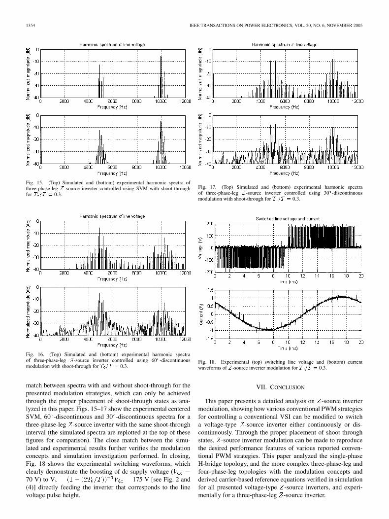
Fig. 15. (Top) Simulated and (bottom) experimental harmonic spectra ofthree-phase-leg Z-source inverter controlled using SVM with shoot-throughfor T =T = 0.3.
Fig. 16. (Top) Simulated and (bottom) experimental harmonic spectraof three-phase-leg Z-source inverter controlled using 60 -discontinuousmodulation with shoot-through for T =T = 0.3.
match between spectra with and without shoot-through for thepresented modulation strategies, which can only be achievedthrough the proper placement of shoot-through states as ana-lyzed in this paper. Figs. 15–17 show the experimental centeredSVM, 60 -discontinuous and 30 -discontinuous spectra for athree-phase-leg -source inverter with the same shoot-throughinterval (the simulated spectra are replotted at the top of thesefigures for comparison). The close match between the simu-lated and experimental results further verifies the modulationconcepts and simulation investigation performed. In closing,Fig. 18 shows the experimental switching waveforms, whichclearly demonstrate the boosting of dc supply voltage (70 V) to V 175 V [see Fig. 2 and(4)] directly feeding the inverter that corresponds to the linevoltage pulse height.
Fig. 17. (Top) Simulated and (bottom) experimental harmonic spectraof three-phase-leg Z-source inverter controlled using 30 -discontinuousmodulation with shoot-through for T =T = 0.3.
Fig. 18. Experimental (top) switching line voltage and (bottom) currentwaveforms of Z-source inverter modulation for T =T = 0.3.
VII. CONCLUSION
This paper presents a detailed analysis on -source invertermodulation, showing how various conventional PWM strategiesfor controlling a conventional VSI can be modified to switcha voltage-type -source inverter either continuously or dis-continuously. Through the proper placement of shoot-throughstates, -source inverter modulation can be made to reproducethe desired performance features of various reported conven-tional PWM strategies. This paper analyzed the single-phaseH-bridge topology, and the more complex three-phase-leg andfour-phase-leg topologies with the modulation concepts andderived carrier-based reference equations verified in simulationfor all presented voltage-type -source inverters, and experi-mentally for a three-phase-leg -source inverter.

LOH et al.: PULSE-WIDTH MODULATION OF -SOURCE INVERTERS 1355
REFERENCES
[1] F. Z. Peng, “Z-source inverter,” IEEE Trans. Ind. Appl., vol. 39, no. 2,pp. 504–510, Mar/Apr. 2003.
[2] D. G. Holmes, “The significance of zero space vector placement for car-rier-based PWM schemes,” IEEE Trans. Ind. Appl., vol. 32, no. 5, pp.1122–1129, Sep./Oct. 1996.
[3] A. M. Hava, R. J. Kerkman, and T. A. Lipo, “Simple analytical andgraphical methods for carrier-based PWM-VSI drives,” IEEE Trans.Power Electron., vol. 14, no. 1, pp. 49–61, Jan. 1999.
[4] J. Holtz, “Pulse width modulation—a survey,” IEEE Trans. Ind. Elec-tron., vol. 39, no. 6, pp. 410–420, Dec. 1992.
[5] S. R. Bowes and Y. S. Lai, “Investigation into optimizing high switchingfrequency regular sampled PWM control for drives and static power con-verters,” Proc. Inst. Elect. Eng., vol. 143, pp. 282–293, Jul. 1996.
[6] P. C. Loh and D. G. Holmes, “A multidimensional variable band fluxmodulator for four phase-leg voltage source inverters,” IEEE Trans.Power Electron., vol. 18, no. 2, pp. 628–635, Mar. 2003.
Poh Chiang Loh (S’01–M’04) received the B.Eng(with honors) and M.Eng degrees from the NationalUniversity of Singapore, in 1998 and 2000, respec-tively, and the Ph.D. degree from Monash Univer-sity, Victoria, Australia, in 2002, all in electrical en-gineering.
During the Summer of 2001, he was a VisitingScholar with the Wisconsin Electric Machineand Power Electronics Consortium, Universityof Wisconsin, Madison, where he worked on thesynchronized implementation of cascaded multilevel
inverters, and reduced common mode carrier-based and hysteresis controlstrategies for multilevel inverters. From 2002 to 2003, he was a Project Engineerwith the Defence Science and Technology Agency, Singapore, managing majordefence infrastructure projects and exploring new technology for intelligentdefense applications. Since 2003, he has been an Assistant Professor withNanyang Technological University, Singapore.
D. Mahinda Vilathgamuwa (S’90–M’93–SM’99)received the B.Sc. degree in electrical engineeringfrom the University of Moratuwa, Moratuwa, SriLanka, in 1985 and the Ph.D. degree in electricalengineering from Cambridge University, Cambridge,UK, in 1993.
He joined the School of Electrical and ElectronicEngineering, Nanyang Technological University,Singapore, in 1993 as a Lecturer and where he isnow an Associate Professor. He has published morethan 80 research papers in refereed journals and
conferences. His research interests are power electronic converters, electricaldrives, and power quality.
Dr Vilathgamuwa is the co-Chairman of the Power Electronics and DrivesSystems Conference 2005 (PEDS’05).
Yue Sen Lai received the B.Eng degree (withhonors) in electrical and electronic engineering fromthe Nanyang Technological University, Singapore,in 2004.
He is now with A Lighting Enterprise, Singapore,as a Manager.
Geok Tin Chua received the B.Eng degree (withhonors) in electrical and electronic engineering fromthe Nanyang Technological University, Singapore,in 2004.
She is now undergoing engineering training withthe Economic and Development Board (Singapore)Attachment Program, Kanagawa, Japan.
Yunwei Li (S’04) received the B.Eng degree in elec-trical engineering from Tianjin University, Tianjin,China, in 2002 and is currently pursuing the Ph.D.degree in the School of Electrical and Electronic En-gineering, Nanyang Technological University, Singa-pore.
From February to August 2005, he was attached tothe Institute of Energy Technology, Aalborg Univer-sity, Aalborg, Denmark, as a Visiting Scholar.
Mr. Li is a member of the IEEE Industrial Appli-cation Society.