06- diff amp mosfet.ppt - universiti tenaga nasionalmetalab.uniten.edu.my/~jamaludin/eeeb273 n06-...
TRANSCRIPT
EEEB273 – Electronics Analysis & Design II
Lecturer: Dr Jamaludin Bin Omar 6-1
MOSFET Differential
PairReference: Neamen, Chapter 11
(6)
�
Learning Outcome
Able to: • Describe the mechanism by which a
differential-mode signal and common-mode signal are produced in a MOSFET differential-amplifier.
• Describe the dc transfer characteristics of a MOSFET differential-amplifier.
�
�
6.0) Essential Formulas
Region NMOS PMOS
Saturation vDS� vDS����� vSD� vSD�����
Transition Point
vDS����� ��vGS � VTN vSD����� ��vSG ��VTP
2][ TPSGpD VvKi +=2][ TNGSnD VvKi −=
oxoxox
poxpp
noxnn
tCL
Wk
L
WCK
LWk
LWC
K
ε
µ
µ
=
⋅==
⋅==
22
22'
' µn , µpMobility of electrons, holes
�oxOxide permittivity
toxOxide thickness
W, L Channel Width� Length
kn’ = µn Coxkp’ = µp Cox
Process conduction parameter (provided by manufacturer) �
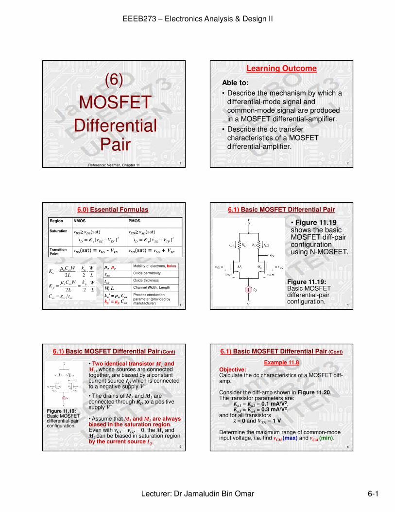
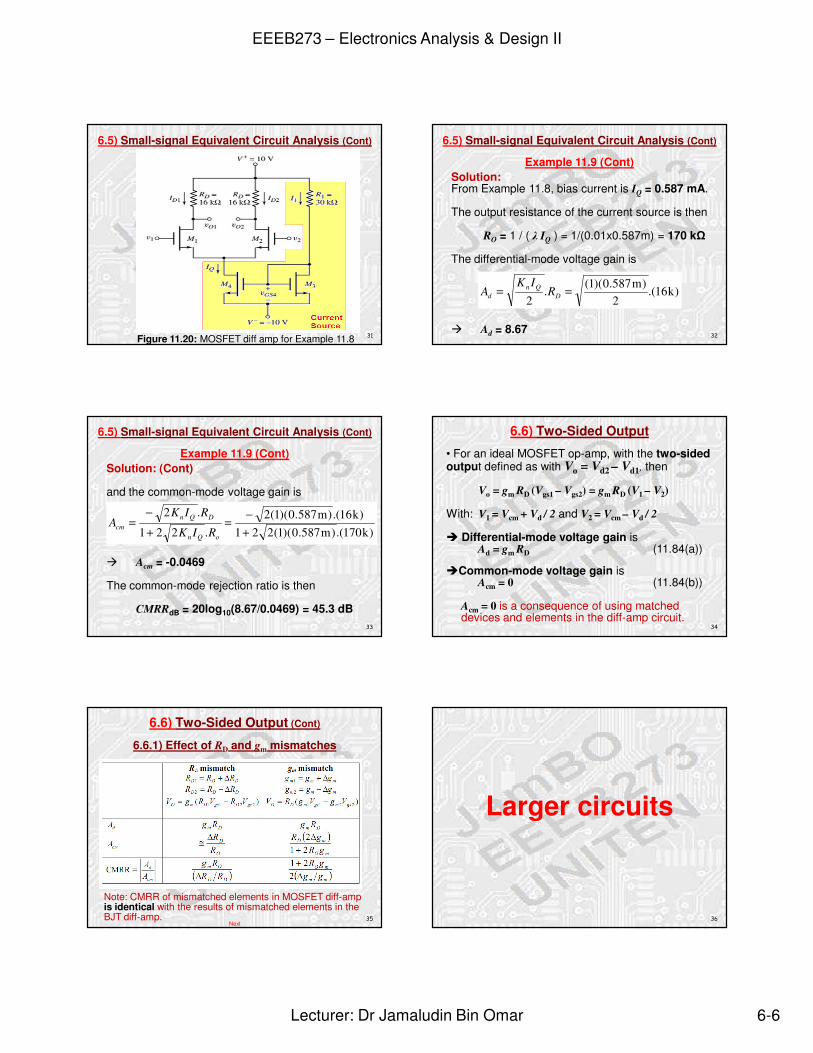
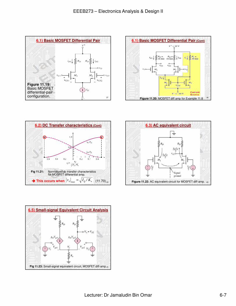
• Figure 11.19shows the basic MOSFET diff-pair configuration using N-MOSFET.
6.1) Basic MOSFET Differential Pair
Figure 11.19: Basic MOSFET differential-pair configuration.
�
6.1) Basic MOSFET Differential Pair (Cont)
Figure 11.19: Basic MOSFET differential-pair configuration.
• Two identical transistor M1 and M2, whose sources are connected together, are biased by a constant current source IQ which is connected to a negative supply V_
• The drains of M1 and M2 are connected through RD to a positive supply V+
• Assume that M1 and M2 are always biased in the saturation region. Even with vG1 = vG2 = 0, the M1 and M2 can be biased in saturation region by the current source IQ.
�
6.1) Basic MOSFET Differential Pair (Cont)
Example 11.8Objective:Calculate the dc characteristics of a MOSFET diff-amp.
Consider the diff-amp shown in Figure 11.20. The transistor parameters are:
Kn1 = Kn2 = 0.1 mA/V2,Kn3 = Kn4 = 0.3 mA/V2,
and for all transistors� = 0 and VTN = 1 V
Determine the maximum range of common-mode input voltage, i.e. find vCM (max) and vCM (min).

EEEB273 – Electronics Analysis & Design II
Lecturer: Dr Jamaludin Bin Omar 6-2
�
6.1) Basic MOSFET Differential Pair (Cont)
Example 11.8 (Cont)
Figure 11.20: MOSFET diff amp for Example 11.8
6.1) Basic MOSFET Differential Pair (Cont)
Example 11.8 (Cont)
Figure 11.20: MOSFET diff amp for Example 11.8
6.1) Basic MOSFET Differential Pair (Cont)
Example 11.8 (Cont)Solution:The reference current can be determined from:
and from
Thus
Yields
and
( )
mA587.0
V40.2
011179
20
1
4
42
4
2431
1
4
1
41
==
=−−
−=
−=−−=−+
I
V
VV
VVKI
RV
RVVV
I
GS
GSGS
TNGSn
GSGS
��
6.1) Basic MOSFET Differential Pair (Cont)
Example 11.8 (Cont)The quiescent drain currents in M1 and M2 :
ID1 = ID2 = IQ / 2 � 0.293 mA
The gate-to-source voltages are then
The quiescent values of vO1 and vO2 are
vO1 = vO2 = V+ – ID1 RD / 2
= 10 – (0.293m)(16k)/2 = 5.31 V
V71.211.0
293.0
1
121 =+=+== TN
n
DGSGS V
KI
VV
��
6.1) Basic MOSFET Differential Pair (Cont)
Example 11.8 (Cont)
��
6.1) Basic MOSFET Differential Pair (Cont)
Example 11.8 (Cont)The maximum common-mode input voltage is the value when M1 and M2 reach the transition point
vCM (max) = VS1(max) + VGS1= (vO1 - VDS1(sat)) + VGS1
The minimum common-mode input voltage is the value when M4 reaches the transition point
vCM (min) = VS1(min) + VGS1= (V-- + VDS4(sat)) + VGS1
EEEB273 – Electronics Analysis & Design II
Lecturer: Dr Jamaludin Bin Omar 6-3
��
6.1) Basic MOSFET Differential Pair (Cont)
Example 11.8 (Cont)The maximum common-mode input voltage is the value when M1 and M2 reach the transition point,
VDS1 = VDS2 = VDS1(sat) = VGS1 - VTNVDS1 = 2.71 - 1 = 1.71 V
Therefore,vCM (max) = vO1 - VDS1(sat) + VGS1
= 5.31 - 1.71 + 2.71 = 6.31 V
The minimum common-mode input voltage is the value when M4 reaches the transition point,
VDS4 = VDS4(sat) = VGS4 - VTN = 2.4 - 1 = 1.4 VTherefore,
vCM (min) = V-- + VDS4(sat) + VGS1= (-10) + 1.4 + 2.71 = -5.89 V
( )( )
( )2121
2121
222
211
.
GSGSGGd
dnGSGSnDD
TNGSnD
TNGSnD
vvvvv
vKvvKii
VvKi
VvKi
−=−==−=−
−=
−=
��
6.2) DC Transfer characteristics
• Use circuit in Figure 11.19. Assume M1 and M2 are matched and neglecting their output resistances:
(11.60(a))
(11.60(b))
Taking square roots and subtracting
where (11.61)
is the differential-mode input voltage.
��
6.2) DC Transfer characteristics (Cont)
• If vd > 0, then vG1 > vG2 and vGS1 > vGS2
which implies that iD1 > iD2
• Since iD1 + iD2 = IQ (11.62)
( ) ( )( ) ( )
( ) 041
21
.
221
21
211
222
11
=−+−
−=−
==−−
dnQDQD
dnQDQD
dndnDQD
vKIiIi
vKIiIi
vKvKiIi
22
21
21.
22
21.
22
dQ
nd
QnQD
dQ
nd
QnQD
vI
Kv
IKIi
vI
Kv
IKIi
��
�
�
��
�
�−−=
��
�
�
��
�
�−+=
��
6.2) DC Transfer characteristics (Cont)
• Applying the quadratic formula, rearranging terms, and noting that iD1 > IQ / 2 and vd > 0, can obtain
(11.66)
• Using Equation (11.62) can also obtain
(11.67)
��
6.2) DC Transfer characteristics (Cont)
• The normalized drain currents are
(11.68)
and (11.69)
� These equations describe the dc transfer characteristics for the circuit. They are plotted in Figure 11.21 as a function of normalized differential input voltage
22
21
21.
221
21.
221
dQ
nd
Q
n
Q
D
dQ
nd
Q
n
Q
D
vI
Kv
IK
Ii
vI
Kv
IK
Ii
��
�
�
��
�
�−−=
��
�
�
��
�
�−+=
( )nQd KIv /2/�
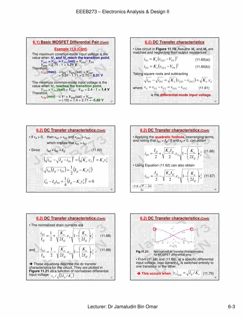
6.2) DC Transfer characteristics (Cont)
• From (11.68) and (11.69), at a specific differential input voltage, bias current IQ is switched entirely to one transistor or the other.
���� This occurs when (11.70)
Fig 11.21: Normalized dc transfer characteristics for MOSFET differential amp.
nQd KIv /max
=
EEEB273 – Electronics Analysis & Design II
Lecturer: Dr Jamaludin Bin Omar 6-4
• Forward transconductance = the slope of the dc transfer characteristics for the iD1 curve.• From Figure 11.21, maximum forward transconductance occurs at vd = 0, so that
(11.71)
• Using (11.66),
(11.72)
where gm is each transistor’s transconductance.
22(max)
(max)0
1
mQnf
vd
Df
gIKg
dvdi
gd
==
==
�
6.2) DC Transfer characteristics (Cont)
��
6.2) DC Transfer characteristics (Cont)
• The slope of iD2 characteristic curve at vd = 0 is the same, except negative.
Note:
• Similar to BJT diff-amp, the differential-mode input voltage must be held within a small range of voltages so as to remain linear.
• However, the vd(max) for the MOSFET diff-amp is much larger than vd(max) for the BJT diff-amp.Why? Because the gain of the MOSFET diff-amp is much smaller than the gain of the bipolar (BJT) diff-amp.
Next
��
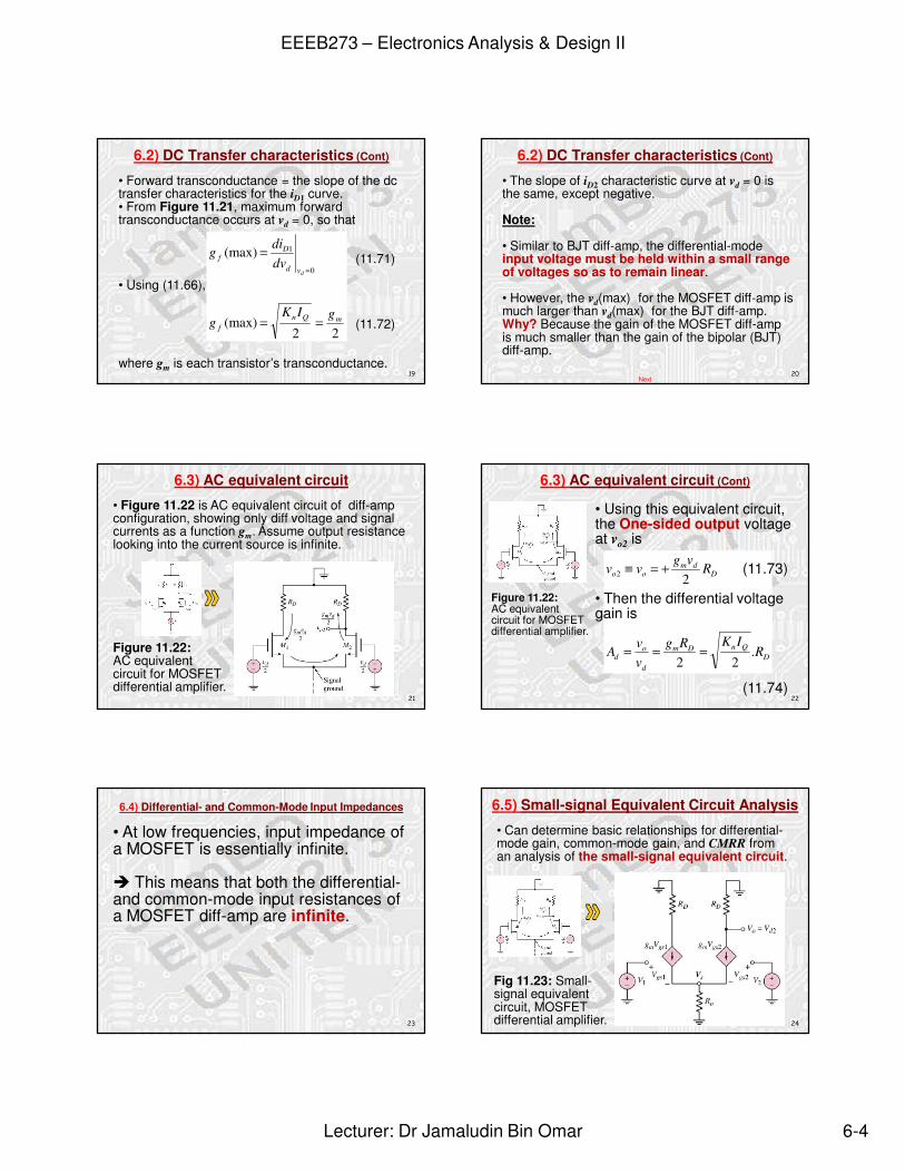
• Figure 11.22 is AC equivalent circuit of diff-amp configuration, showing only diff voltage and signal currents as a function gm. Assume output resistance looking into the current source is infinite.
6.3) AC equivalent circuit
Figure 11.22: AC equivalent circuit for MOSFET differential amplifier.
DQnDm
d
od
Ddm
oo
RIKRg
vv
A
Rvg
vv
.22
22
===
+=≡
• Using this equivalent circuit, the One-sided output voltage at vo2 is
(11.73)
• Then the differential voltage gain is
(11.74)��
6.3) AC equivalent circuit (Cont)
Figure 11.22: AC equivalent circuit for MOSFET differential amplifier.
��
6.4) Differential- and Common-Mode Input Impedances
• At low frequencies, input impedance of a MOSFET is essentially infinite.
� This means that both the differential-and common-mode input resistances of a MOSFET diff-amp are infinite.
��
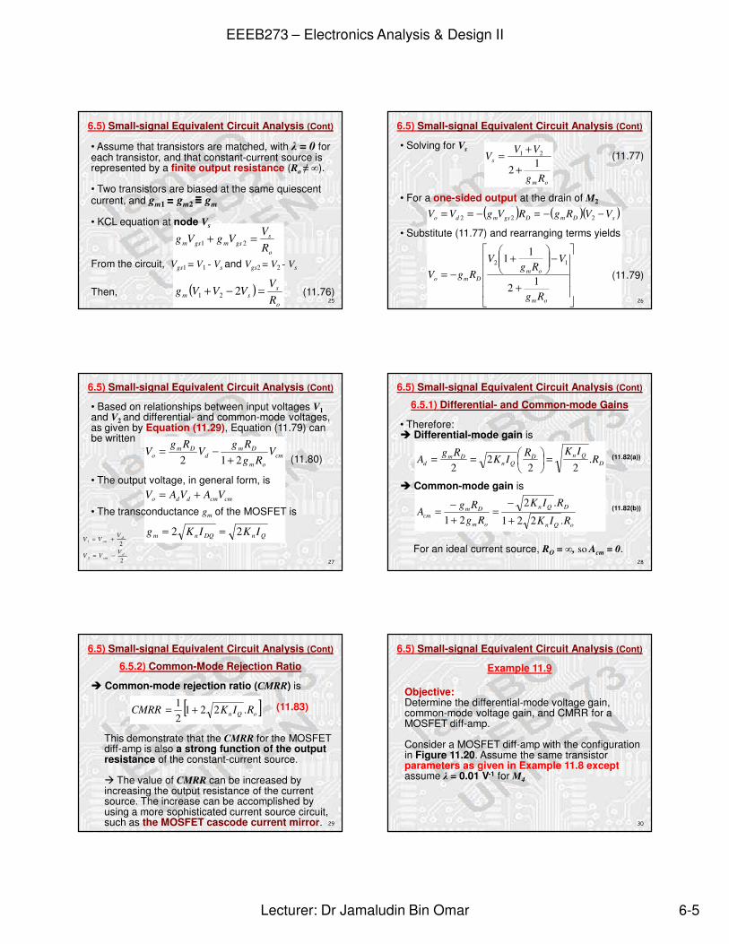
6.5) Small-signal Equivalent Circuit Analysis
• Can determine basic relationships for differential-mode gain, common-mode gain, and CMRR from an analysis of the small-signal equivalent circuit.
Fig 11.23: Small-signal equivalent circuit, MOSFET differential amplifier.
EEEB273 – Electronics Analysis & Design II
Lecturer: Dr Jamaludin Bin Omar 6-5
( )o
ssm
o
sgsmgsm
RV
VVVg
RV
VgVg
=−+
=+
221
21
��
6.5) Small-signal Equivalent Circuit Analysis (Cont)
• Assume that transistors are matched, with � = 0 for each transistor, and that constant-current source is represented by a finite output resistance (Ro � �).
• Two transistors are biased at the same quiescent current, and gm1 = gm2 � gm
• KCL equation at node Vs
From the circuit, Vgs1 = V1 - Vs and Vgs2 = V2 - Vs
Then, (11.76)
( ) ( )( )
����
�
�
�
+
−���
����
�+
−=
−−=−==
om
omDmo
sDmDgsmdo
Rg
VRg
VRgV
VVRgRVgVV
12
11 12
222
��
6.5) Small-signal Equivalent Circuit Analysis (Cont)
• Solving for Vs(11.77)
• For a one-sided output at the drain of M2
• Substitute (11.77) and rearranging terms yields
(11.79)
om
s
Rg
VVV
12
21
+
+=
QnDQnm
cmcmddo
cmom
Dmd
Dmo
IKIKg
VAVAV
VRg
RgV
RgV
22
212
==
+=
+−=
��
6.5) Small-signal Equivalent Circuit Analysis (Cont)
• Based on relationships between input voltages V1and V2 and differential- and common-mode voltages, as given by Equation (11.29), Equation (11.79) can be written
(11.80)
• The output voltage, in general form, is
• The transconductance gm of the MOSFET is
2
2
2
1
dcm
dcm
VVV
VVV
−=
+=
oQn
DQn
om
Dmcm
DQnD
QnDm
d
RIK
RIK
RgRg
A
RIKR
IKRg
A
.221
.2
21
.22
22
+−
=+−=
=��
���
�==
• Therefore:� Differential-mode gain is
(11.82(a))
� Common-mode gain is
(11.82(b))
For an ideal current source, RO = �, so Acm = 0.�
6.5.1) Differential- and Common-mode Gains
6.5) Small-signal Equivalent Circuit Analysis (Cont)
�
6.5.2) Common-Mode Rejection Ratio
� Common-mode rejection ratio (CMRR) is
(11.83)
This demonstrate that the CMRR for the MOSFET diff-amp is also a strong function of the output resistance of the constant-current source.
� The value of CMRR can be increased by increasing the output resistance of the current source. The increase can be accomplished by using a more sophisticated current source circuit, such as the MOSFET cascode current mirror.
[ ]oQn RIKCMRR .22121 +=
6.5) Small-signal Equivalent Circuit Analysis (Cont)
��
6.5) Small-signal Equivalent Circuit Analysis (Cont)
Example 11.9
Objective:Determine the differential-mode voltage gain, common-mode voltage gain, and CMRR for a MOSFET diff-amp.
Consider a MOSFET diff-amp with the configuration in Figure 11.20. Assume the same transistor parameters as given in Example 11.8 except assume � = 0.01 V-1 for M4
EEEB273 – Electronics Analysis & Design II
Lecturer: Dr Jamaludin Bin Omar 6-6
��
6.5) Small-signal Equivalent Circuit Analysis (Cont)
Figure 11.20: MOSFET diff amp for Example 11.8 ��
6.5) Small-signal Equivalent Circuit Analysis (Cont)
Example 11.9 (Cont)Solution:From Example 11.8, bias current is IQ = 0.587 mA.
The output resistance of the current source is then
RO = 1 / ( � IQ ) = 1/(0.01x0.587m) = 170 k�
The differential-mode voltage gain is
� Ad = 8.67
)k16.(2
)m587.0)(1(.
2== D
Qnd R
IKA
��
6.5) Small-signal Equivalent Circuit Analysis (Cont)
Example 11.9 (Cont)Solution: (Cont)
and the common-mode voltage gain is
� Acm = -0.0469
The common-mode rejection ratio is then
CMRRdB = 20log10(8.67/0.0469) = 45.3 dB
)k170.()m587.0)(1(221)k16.()m587.0)(1(2
.221
.2
+−=
+
−=
oQn
DQncm RIK
RIKA
��
6.6) Two-Sided Output
• For an ideal MOSFET op-amp, with the two-sided output defined as with Vo = Vd2 – Vd1, then
Vo = gm RD (Vgs1 – Vgs2) = gm RD (V1 – V2)
With: V1 = Vcm + Vd / 2 and V2 = Vcm – Vd / 2
� Differential-mode voltage gain isAd = gm RD (11.84(a))
�Common-mode voltage gain isAcm = 0 (11.84(b))
Acm = 0 is a consequence of using matched devices and elements in the diff-amp circuit.
��
6.6) Two-Sided Output (Cont)
6.6.1) Effect of RD and gm mismatches
Note: CMRR of mismatched elements in MOSFET diff-amp is identical with the results of mismatched elements in the BJT diff-amp.
Next��
Larger circuits
EEEB273 – Electronics Analysis & Design II
Lecturer: Dr Jamaludin Bin Omar 6-7
��
6.1) Basic MOSFET Differential Pair
Figure 11.19: Basic MOSFET differential-pair configuration. �
6.1) Basic MOSFET Differential Pair (Cont)
Figure 11.20: MOSFET diff amp for Example 11.8
�
6.2) DC Transfer characteristics (Cont)
���� This occurs when (11.70)
Fig 11.21: Normalized dc transfer characteristics for MOSFET differential amp.
nQd KIv /max
=��
6.3) AC equivalent circuit
Figure 11.22: AC equivalent circuit for MOSFET diff-amp.
��
6.5) Small-signal Equivalent Circuit Analysis
Fig 11.23: Small-signal equivalent circuit, MOSFET diff-amp.