0e0 preamble 0 - viinstruments 0 1850a and 1855a
TRANSCRIPT

000e00000000000000000000000e0000000e00e0e0ee
pREAMBLE- VIINSTRUMENTS
1850A and 1855A
DIFFERENTIAL AMPLIFIERS
March 10, 1999
PREAMBLE INSTRUMENTS, Inc,P.O. Box 6118Beaverton, OR 97007-0118

0000000000000000000000000000000000000000000O
03-10-99
TABLE OF CONTENTS
Section 1 SPECIFICATIONS
Introduction ............................................................................. 1 - l
1850/1855A Specifications ...................................................... 1-2
Power Requirements & Physical Characteristics ..................... 1-3
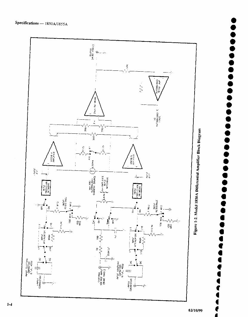
1850 Block Diagram ................................................................ 1-4
1855A Block Diagram ............................................................. 1-5
Section 2 OPERATING INSTRUCTIONS,CONTROLS AND INDICATORS
Front Panel ...............................................................................2-1
Rear Panel ................................................................................2-4
New Features of 1850A and 1855A ......................................... 2-5
Oscilloscope Settings ............................................................... 2-6
Model 1850 Operation ............................................................. 2-7
Section 3 GENERAL OPERATING INFORMATION
Getting Started ......................................................................... 3-1
Power Connection .................................................................... 3-1
1855A Front Panel Operation .................................................. 3- I
Attenuator and Gain Operation ................................................ 3-1
Comparison Voltage Operation ............................................... 3-2
Differential Offset Operation ................................................... 3-3
Which Offset Mode Should Be Used? ..................................... 3-4
Operator Traps to Avoid .......................................................... 3-4
1850A/1855A

1850A/1855A
INITIAL SCOPE AND 1855 SETUP
L_ .............
7---- ’ ........
~---
i ’
SELECT 50 OHM INPUTOR
PROVIDE 60 OHM TERMINATOR
~,.~50mV/I)fV
Iv ~.ImV/DIV
Posmo
"~’ SET SENSITMTY TO 50mVldiv
DURING OPgRA13ON. USEON LY 5OmvIoN ON
MORE SENSITIVE PosmoN$
POSITION TRACE TO CENTER <SCREEN (DC OFFSET = OFF)
00 NOT USE TH E SCOPEPOSmON OR OFFSE’f
AFrER THIS INIT~L SETUP
~ AC
/ ~, ’f oc ’~ o:
//,!
///’ @ SELECT DCINPUTCOUPLING//
s
’ /
/
//,/
CONNECT AMPLIFIER OUTPUT TOSCOPE INPUT WITH 50 OHM COAX
~
......... mE
LJ ~e~ ~ ~ ~ ’ ’~’ --"~< "
/,
l g ] ATTACH XCl00 PROBES ~ ~’2"
DO NOT ADJUST PROBE COMPENSATION~THOUT FIRST REFERRING TO THE MANUAL
TRACE ON ~COPEUSE VDIFF AND PVG TO POSITION
~i PVG DI|PLAYS THS VOLTAGE OF THE SIGNAL AS ffPASSES THROUGH THE SCOPE DIEPLAY CENTERLIRE.
(RE~IRRED TO THE PROIE I~P)
CONNECT PROBE CODING LEAD TOPROBE CODE INPUT ON 1866 REAR PANEL
ii 03116/99
eooiieeeeooeeeeeooeoeoeoooi)ooeeoooooeeoooooo

00000000000
Specifications- 1850A/1855A
SECTION 1SPECIFICATIONS
0000000000000000000000000
00000000
INTRODUCTION
The 1850A and 1855A are stand-alone high performance100MHz differential amplifiers. They are intended to actas signal conditioning preamplifiers for oscilloscopes, digi-tizers, network analyzers and spectrum analyzers, providingdifferential measurement capability to instruments havingonly a single-ended input. When used with an1850A/1855A, most good quality oscilloscopes can obtainCommon Mode Rejection Ratio (CMRR) and overdriverecovery performance that was previously unobtainable in¯ any product.
Amplifier gain may be set to 1 or 10. A built-in input at-tenuator may be separately set to attenuate signals by afactor of 10, allowing gains of 10, I, or 0.1 and commonmode dynamic range of_15.5V (+1) or +_.155V (+10). tional probes increase the maximum input signal and com-mon mode ranges in proportion to their attenuation ratio,but not exceeding their maximum input voltage rating.Effective gain of the 1855A, including probe attenuation,amplifier gain and attenuator settings, is automatically dis-played.
The 1855A has a bandwidth of 100 MHz, but any one ofthe three 3-pole bandwidth limit filters may be selected toreduce bandwidth to 20MHz, IMHz or 100kHz to limitnoise above the frequency of interest.
03/i 0/99
The 1850A/1855A output is carefully limited at +500mVso that the oscilloscope is not overdriven by large inputs.This allows many oscilloscopes to directly measure thesettling of D/A converters with 14 bit (60ppm) precision,better than any other differential comparator.
The 1855A features a built-in Precision Voltage Generator(PVG) that can be set to any voltage between +15.5 volts(+10 volts in Differential Offset mode) with 100~tV resolu-tion. Each digit of the voltage generator output can be in-dividually incremented or decremented and the signchanged between + and -. The PVG’s output can be se-lected as an input to the inverting (-) input of the amplifierfor operation as a differential comparator or applied inter-nally as a true differential offset voltage. The voltage isalso available to be used externally through a rear panelconnector. On the 1850A, this connector becomes an inputthrough which the user can apply an external voltage toachieve the same differential offset and comparison func-tions.
The 1850A/1855A operates from 100 to 250 VAC linewithout line switching.
High performance differential probes such as the PreambleInstruments XC100 10X/100X high CMRR probes are rec-ommended.
i-1

Specifications m 1850A/1855A
1850A/1855A SPECIFICATIONS
GENERAL:Amplifier gain:Gain accuracy:Bandwidth:Rise time:Output impedance:Intended output load:Maximum output:Input attenuation:+10 ATTENUATOR accumc3.,:Max differential linear input:
(X10 GAIN, +1 ATTENUATOR):(X1 GAIN, +1 ATTENUATOR)(X10 GAIN, +I0 ATTENUATOR)(X1 GAIN, +10 ATTENUATOR)
Maximum input slew rate:(+1 ATTENUATOR. X1 probe):(+Ill ATTENUATOR or X10 probe):(+10 ATTENUATOR and X10 probe):(+1 ATTENUATOR and XI00 probe):(+Ill ATTENUATOR and X100 probe):
Input noise (X10 GAIN):DC drift (X10 GAIN):Common mode rejection ratio:Max common mode input:
(+1 ATTENUATOR):(+Ill ATTENUATOR):(+10 ATTENUATOR and X10 probe)
Input resistance:
(+1 ATTENUATOR. X1 or X10 GAIN):(+10 ATTENUATOR. X1 or X10 GAIN):
Input capacitance (+1 or +10 ATTENUATOR):Bandwidth limit filters (1855A only):Filter characteristics ~ 1855A only):+INPUT selections:-INPUT selections:Input coupling capacitor:Input gate current (X1 and X10 GAIN, +1 ATTENUATOR):Input protection:
DIFFERENTIAL OFFSET (VDIFF) MODE:Differential offset range (referred to input):
(X10 GAIN, +I ATrENUATOR):(X1 GAIN, +1 ATTENUATOR):(XI0 GAIN, +10 ATTENUATOR):(X1 GAIN, +10 ATTENUATOR):(XI GAIN, +10 ATTENUATOR. X10 probe)
Differential offset accuracy:(X10 GAIN, +I ATTENUATOR):(X1 GAIN, +1 ATTENUATOR):(X10 GAIN, +10 ATTENUATOR):(XI GAIN, +10 ATTENUATOR):
1-2
1 orl0+_1%
>I00MHz<3.5ns
50 ohms50 ohms
limited at +0.50V into 50 ohms+1 or +10
_+0.05%
N).O5V or +0.5V with XIO probeN).5 or +5.0V with XIO probe_+0.5 or +-5.0V with XIO probe_+5.0 or +50V with XIO probe
O. 5 V/ns5.0V/ns50V/ns50V/ns
500V/ns<4nV/sq rt Hz. broadband
50~V/°CSee Figure 1-1
+15.5V (X1 or X10 GAIN)+-I55V(X1 or X10 GAIN)
+l.55kV(Xl or X10 GAIN)
1 megohm or 100 megohms1 megohm
20pF20MHz. 1.0MHz and 100kHz
18dB/octave (3-pole Bessel)AC, OFF (Pmtegra),
AC, OFF (precharge), DC, Vco~0.1 ~tF, 400VDC<10pA. 0-45°C
protected to +_250V, automatic input disconnect withmanual reset
+-lV+IOV+-IOV
+lOOV+l.OkV
0.1% + 50V0.1% + 500V
0.15% + 500V0.15% + 5mV
03/10/99

00000000000000000000000000000000000000000000
COMPARISON OFFSET (Vco~tp) MODE:
Effective comparison voltage range:
(+1 ATTENUATOR):(+10 ATTENUATOR):(Xl0 probe and +10 ATTENUATOR):
PRECISION VOLTAGE SOURCE (1855A only):
Output range:DC accuracy:Resolution:Control:Temperature coefficient:Type:Output:PVG AUTO ZERO:
POWER REQUIREMENTS
Line voltage requirement:Line frequency range:Power requirement:
ENVIRONMENTAL CHARACTERISTICS
Operating Range:Non-Operating:
PHYSICAL CHARACTERISTICS
Height:Width:Depth:Weight:Shipping Weight:
Specifications- 1850A/1855A
’_15.5V (Xl or Xl0 GAIN)+155V (Xl or Xl0 GAIN)1.55kV (Xl or Xl0 GAIN)
+15.5V0.05% of reading +500~V (0° to 50°C)
100~tVAll digits are addressable. Digit carries to next decade
typically <5ppm/°C of full scaleOven stabilized buried Zener
Applied to inverting input and available at rear panelSets output to zero when 0.0 volts selected andin error by more than 0.5mV thereafter
100 to 250VAC48 - 66Hz
35 W maximum
0 to 50°C-40 to 75°C
7,29cm (2.87")21.2cm (8.36")23.2cm (9.12")2.15kg (4.751b)3.12kg (6.881b)
cMRR
1000000
100000
~-- iIi.1000~
1000
i100 :
i , ’ i i
|0 I
I AMPLIF’IER SE’I’T1NGS
t XI OR Xl0 GAIN. XI Aq~’ENUATOR L
1 RHz 10 kHz 100 kHz 1 MHz 10 MHz 100 MHz
Figure 1-1. CMRR vs Frequency
1131111199 1-3
1-4
Specifications ~ 1850A/1855A
03110199
OOOOOOOOOOOO0OOOOOO0OO
|
OOOOeOIIO

00000000000000000000000000000000000@00
03/10/99
Specifications- 1850A/1855A
\

00090000000000000000000000000000000000000000
Operating Instructions, Controls and Indicators-- 1850A/1855A
SECTION 2OPERATING INSTRUCTIONS, CONTROLS
AND INDICATORS
FRONTPANEL
ATTENUATOR
Signals connected to the +INPUT and the -INPUT areconnected either directly to the 1850A/1855A’s amplifierinputs or to the input attenuators. The input attenuators arepassive networks which divide each signal by ten.
In +1 mode the front panel input connectors are directlyconnected to the 1850A/1855A amplifier’s differential in-puts.
In +10 mode each front panel input connector is connectedto a passive 1 megohm attenuator. The attenuator output isconnected to the 1850A/1855A amplifier’s correspondingdifferential input. The signal at each input is attenuated bva factor of ten.
GAIN
The 1850A/1855A amplifier gain (amplification) is select-able between XI and Xl0. The amplified signal appears atthe rear panel AMPLIFIER OUTPUT connector.
A signal connected to the +INPUT will maintain its polar-ity at the output connector. A signal connected to the-INPUT will be inverted in polarity.
Proper gain is obtained when the 1850A/1855A drives a 50ohm load such as an oscilloscope with input impedance setto 50 ohms. An oscilloscope with only a 1 megohm inputimpedance available should have a 50 ohm coaxial termi-nation placed on its input connector. The 1850A/1855A isthen connected to the oscilloscope through the coa.,dal ter-mination.
The amplifier gain and the input attenuator are individuallyselectable to provide versatility. For example, the compari-son voltage range is changed from +15.5000 to +155.000volts by changing the ATTENUATOR from +1 to +10.The overall gain can still be set to either 1 or 0.1 by select-ing the GAIN mode, Xl0 or Xl, as desired.
AUTO ZERO is a feature invoked when either the Xl orXl0 button is pushed, even if a different gain is not se-lected. AUTO ZERO momentarily sets the input couplingto OFF and determines the offset necessary, to set the out-put at 0 volts within about 25~V. During this process the
front panel is unresponsive. When finished, the input cou-pling returns to its previous mode. AUTO ZERO usuallytakes less than one second. This handv feature allows theoperator to DC balance the 1850A/1855A simply by push-ing the GAIN button which is already illuminated. Whenchanging gains, the AUTO ZERO feature is automaticallyinvoked, freshly adjusting the amplifier’s DC balance.
+INPUT COUPLING (AC OFF DC)
,oo .cZ% ~, ,_2~
In OFF mode, the input connector is disconnected from theamplifier input_ and the amplifier input is connected toground. The AC coupling capacitor is connected betweenthe +INPUT and ground through 1 megohm (either theinput attenuator or the input resistor), independent of theINPUT RESISTANCE selected. In this mode, the ACcoupling capacitor is quickly charged to the average DCinput voltage. OFF mode is also referred to as prechargemode. Precharge is particularly useful when planning toAC couple and measure voltages in excess of 19 volts. The1850A/1855A input coupling is set to OFF and connectedto the circuit under test. When the +INPUT is changedfrom OFF to AC mode, the coupling capacitor is alreadycharged, and the trace properly centered on the oscilloscopescreen. Additionally, the risk of tripping the input overloaddetector and automatically disconnecting the input is elimi-nated.
In the AC mode, the +INPUT is connected through an ACcoupling capacitor to the amplifier input or the input at-tenuator. The coupling capacitor retains its charge when theinput is switched to I)C, making it possible to return to thesame circuit without the precharge time. But this alsomakes it possible to discharge the coupling capacitor intoanother circuit under test if its DC voltage differs by morethan approximately 19 volts from the voltage on the cou-pling capacitor. The discharge current is limited to about70mA, but this could damage some circuits. It is therefore
03/10/99 2-1

Operating Instructions, Controls and Indicators-- 1850A/1855A
recommended that the +INPUT coupling first be changedto OFF (precharge) when measuring a new circuit point.This will safely recharge the AC coupling capacitor in lessthan 0.3 seconds. The AC coupling capacitor is 0. I~F andrated at 400VDC.
DC and low frequencies are attenuated by the AC couplingcapacitor and the input resistance. With the ATTEN-UATOR set to +Ill, or set to +1 with the INPUTRESISTANCE set to 1 megohm, the low frequency cut off(-3dB point) is approximately 1.6Hz, lower than most os-cilloscopes by a factor of 5. When the input attenuator is setto +1, the INPUT RESISTANCE may be set to I00 me-gohms, and the -3dB point is 0.016Hz. This extremely lowfrequency cut off is often handy in observing low fre-quency noise riding on large (up to 400 volts) DC voltages.
In the DC mode. the +INPUT connector is connected tothe amplifier either directly or through the input attenuator,and the AC and DC attenuation are the same.
-INPUT COUPLING (AC OFF DC Vco~n,)
inverting input. The 1850A/1855A output is therefore zerowhenever these two voltages are equal. For this reason, thevoltage applied to the inverting input is called a comparisonvoltage, Vco.~n,.
Vco.~p is often used to make precise measurements of largesignals by comparing the accurately known Vco,~n, with theunknown signal. It can also be used to measure the actualvoltage at any point of a waveform
PRECISION VOLTAGE GENERATOR (PVG) outputrange is +15.500 volts. The PVG is never attenuated bv theinput attenuator. Attenuation of the +INPUT signal bv the+11) input attenuator will cause the PVG to null out an inputvoltage up to +155.01) volts which is ten times larger thanthe actual PVG voltage. When the 1855A is used with at-tenuating probes that feature readout, the PVG display ischanged to indicate the voltage at the +INPUT probe tipwhich will bring the amplifier output to zero.
The -INPUT connector is not useable when Vco~n, is se-lected.
r~uu ’~ ve~opqrc,S,t3N x --
err
:.’,~AC,VO~
-.’~ 7-=- .....
t-T-7 " <~> ~ utc, r;",c
¯ ~(S,SlANCC
The -INPUT has the same coupling modes as the +INPUTplus one additional option, Vco~, (comparison voltage).
The 1855A generates a voltage controlled by the push but-tons above and below the front panel numerical display.This voltage is called the Precision Voltage Generator(PVG). The 1850A does not have a built-in PVG and theuser must supply a dc voltage in the range of -15.5V to+ 15.5V to the rear panel OFFSET connector.
In Vco~n, mode, the 1855A’s PVG is connected to the am-plifier’s inverting input through an internal filter designedto eliminate radio and television signal interference. The1850A does not have the PVG, but uses an externally sup-plied voltage. See Page 2-6 for Vco~ operation with the1850A.
The 1850A/1855A’s amplifier subtracts the voltage appliedto its inverting input from the voltage applied to its non-
VDxw (differential offset voltage) is an instrument moderather than a type of input coupling. The Vmrr mode ’allowsthe PVG (or an external source in the case of the 1850A) inject an offset signal into the 1850A/1855A while stillusing both inputs for full differential operation. This modecan be used as a position control to move the trace on theoscilloscope screen in preference to using the oscilloscope’sposition or offset control. The oscilloscope’s position andoffset controls should alwavs be set to zero so that the1850A/1855A’s dvnamic range is properly centered. Op-eration of the 1850A/1855A using the VDXW function is thesame as VcoMr except for the following:
¯ The -INPUT remains active, allowing full use of the1850A/1855 A as a differential amplifier.
¯ The maximum range of the PVG (1855A) or the externalsource (1850A) is _+10.000 volts in X1 GAIN and ±1.0000volts in X10 GAIN. The effects of the +10 inputATTENUATOR and probe attenuation are the same aswhen using Vcosn,, i.e., any input attenuation multiplies theeffective offset.
¯ The VDtrV mode offset accuracy is slightly less than thatobtained using Vcosw.
The 1855A’s PVG display is changed to indicate the volt-age that. if applied between the +INPUT and -INPUT,would bring the amplifier output to zero. When the 1855Ais used with attenuating probes which feature readout, thePVG display is scaled to include the effect of probe at-tenuation.
2-2 03110199
OO
OOOOOOOOOOOOOOOOOOOOOOOOOOOOOOOOOOOOOO00O

00000000000000000000000000000000000000000000
Operating Instructions, Controls and Indicators- 1850A/1855A
INPUT RESISTANCE
When the input ATTENUATOR is set to +1. the inputresistance can be increased from 1 megohm to 100 me-gohms. This is advantageous when measuring high imped-ance circuits or when AC coupling is needed with a very.low frequency cut off.
Unbalanced source impedances can have an adverse effecton common mode rejection. For example, a differentialsource with impedances of 1000 and 2000 ohms, eachloaded with 1 megohm will have a common mode rejectionratio (CMRR) of 1000 to I. The common mode rejectionratio can be improved to 100,000 to 1 by using 100 me-gohm input resistance.
This limitation is also apparent when trying to make accu-rate measurements using VcoMP. A 10.000 volt referencewith a I000 ohm output impedance will be reduced to9.9900 volts by the 1850A/1855A 1 megohm input resis-tance, introducing a 10mV error in the measurement. In-creasing the input resistance to 100 megohms decreases thiserror to 1001aV.
Oscilloscope inputs have a small input current which cancause an offset when measuring high impedance circuits.The offset can be observed by opening and shorting theinput to ground. The 1850A/1855A has a temperature-compensated input current pull away (cancellation) whichworks in both the 1 megohm and 100 megohm INPUTRESISTANCE modes. Its input offset current is consid-erably less than that of most oscilloscopes.
EFFECTIVE GAIN (1855A ONLY)
Six lights (LEDs) across the top of the 1855A front panelindicate the total gain from the instrument input to output.When the XI light is lighted, the overall amplifier voltagegain (amplification) is unity. Similarly, XI0 indicates overall amplification of ten times. +10 indicates the voltageamplification is 0. I, and so forth.
When Preamble Instruments or other encoded probes areproperly used. the effective gain includes the probe’s at-tenuation factor.
BW LIMIT (1855A ONLY)
FULL -- The 1855A amplifier’s full bandwidth, over100MHz, is passed to the oscilloscope, spectrum analyzeror digitizer. Frequency response and transient response areessentially independent of the oscilloscope’s input imped-ance.
20MHz h A 20MHz three pole (I 8dB/octave) filter allowsthe 1855A to reduce extraneous noise. This filter is a pas-sive LC design and is intended to drive a 50 ohm load.Without the load, the filter’s frequency response and tran-sient response are altered.
I MHz -- The I MHz filter is of the same design as the10Ml-lz filter, and the same remarks apply.
100kHz h The 100kHz filter is an active filter with a 50ohm output impedance. Transient and frequency responseare independent of the load impedance. An internal adjust-ment minimizes the filter’s DC offset.
PRECISION VOLTAGE GENERATOR (PVG)(1855A ONLY)
The PVG generates the voltage which is used in the Vco,~n,and VD~VV modes and appears at the rear panel OFFSETVOLTAG E (PVG) output connector.
Above each digit is a push button which increments thecorresponding digit by one when pushed. When held, thedigit continues to increment, eventually incrementing thenext higher digit.
Similarly, below each digit is a push button which decre-ments the corresponding digit.
The + button above the left-most digit changes the PVGoutput polarity. The ZERO button below the left-most digitsets the output to zero and invokes the PVG’s AUTOZERO function.
The PVG AUTO ZERO resets the PVG output to zero toeliminate any drift which may have occurred in the PVGdue to low frequency noise, or long term drift. PVG AUTOZERO is invoked each time the ZERO button is pressedand reinvoked as needed if the output exceeds approxi-mately 500uV. The PVG AUTO ZERO only functionswhen the PVG display reads zero.
OVERLOAD
When a signal which could damage the 1850A/1855A hasbeen applied to either input connector, the 1850A/1855Aprotects itself by disconnecting the signal. The input cou-pling mode changes to OFF, and the OVERLOAD light isturned on.
Remove the offending input. The 1850A/1855A is resetand the OVERLOAD light goes out when any of the inputcoupling modes (AC, OFF, or DC) is selected.
When the ATTENUATOR is set to +1, a signal of ap-proximately +19 volts will cause the input to draw currentand the OVERLOAD light to come on. Transients toorapid to be disconnected by the input coupling relay willdraw up to about 70mA of input current. Inputs in excess of250 volts may cause permanent damage to the1850A/I 855A.
03/10/99 2-3

Operating Instructions, Controls and Indicators- 1850A/1855A
The input is not disconnected when the ATTENUATOR isset to +10. The input attenuator is rated at 400 volts maxi-mum continuous input.
REAR PANEL
POWER
Removing the power from the instrument by either turningthe power switch to 0 (off) position or unplugging it willcause the oven to lose power and require time (about 30minutes) for the PVG to stabilize. In high-humidity envi-ronments the time to stabilize may be much longer. In highhumidity environments or when warm-up time inhibits us-age, we recommend that the instrument be left plugged inat all times and the power switch left in the ! (on) position.
Normal instrument operation is obtained with the powerswitch in the 1 (on) position. The instrument reaches itsspecified performance in 30 minutes.
In the 1850A, power is applied when the power switch is inthe 1 (on) position.
PRECISION VOLTAGE GENERATOR OFFSETVOLTAGE (1855A ONLY)
The rear panel OFFSET VOLTAGE BNC (PVG) outputconnector, is a monitor of the Precision Voltage Generator(PVG), It is the same voltage as that applied to the-INPUT when the -INPUT coupling is VcoMP or inter-nally to the 1855A when Valrr is selected. The OFFSETVOLTAGE output can be used either to monitor the PVGwith a digital voltmeter (DVM) or as an input to one more Preamble 1850As or 1855As, There is a 1.59kHzsingle-pole low pass filter between the PVG output and the-INPUT which removes radio frequency interference(RFI). This filter does not attenuate the PVG signal,
The PVG output is not attenuated by the input attenuator orprobes, whereas the input signal is. Therefore the effectiverange of VcoMP is increased by a factor of 10 when the +10ATTENUATOR is selected or a +10 attenuating probe isused to attenuate the input signal. The PVG numerical dis-play reflects the attenuator setting and probe attenuationwhen the probe is readout encoded. As an example, if thereare no probes attached, the +!0 ATTENUATOR is se-lected and the display is set to read -155.000, the PVG out-put will actually be-15.5 volts.
The decimal in the display will be in the correct location toindicate the voltage at the PVG output when no probes areattached and +1 ATTENUATOR and X1 GAIN are se-lected.
The OFFSET VOLTAGE BNC (PVG) output also pres-ents the same voltage used internally for differential offsetwhen Vt~t~ is selected. Because the PVG is applied to theamplifier to create a true differential offset, the relationshipbetween Vanvv and the voltage at the OFFSETVOLTAGE BNC (PVG) output (changes with the ampli-fier gain selection according to the following table:
FRONT PANEL SETTINGS MAXIMUMPVG
GAIN ATTEN VDIFF OUTPUT
XI ÷1 ±lOV ±lOV
Xl ÷1o + 100V ±lOV
XIO +I ±IV +IOV
X 10 +1o _.+10V _+lOV
The maximum Vmvv is multiplied by any probe attenuationfactor. The 1855A front panel displays the correct offsetreferred to the instrument input. When using readout en-coded probes which the 1855A senses, the PVG readoutcalculates the effective differential offset at the probe tip.Of course, both probes must have the same attenuationfactor.
AMPLIFIER OUTPUT
The AMPLIFIER OUTPUT BNC is intended to be usedwith an oscilloscope, spectrum analyzer or digitizer havinga 50 ohm input resistance. The 1850A/1855AAMPLIFIER OUTPUT impedance is 50 ohms. Withoutthe 50 ohm load, the amplifier gain is twice the amountindicated on the front panel. Additionally, the signal pre-sented to an oscilloscope (spectrum analyzer or digitizer) as large as +l volt. This may cause the oscilloscope to sig-nificantly increase its overdrive recovery time, obviatingone of the 1850A/1855A’s important features, fast over-drive recovery.
With the IMHz or 20MHz bandwidth limit filters selected,the 1855A amplifier is not well reverse terminated at highfrequencies. When the oscilloscope’s input impedance is 50ohms, these passive filters work properly.
With FULL or 100kHz bandwidth limit selections, the1855A output impedance is 50 ohms, and the transient re-sponse is independent of whether the oscilloscope termina-tion is present.
2-4 03/10/99
0000000000000O000000000000O0OO0
O

000@@00@00000@000000000000000000000000@00000
Operating Instructions, Controls and Indicators- 1850A/1855A
PROBE CODING INPUT (1855A ONLY)
This jack is to be used with Preamble Instruments probesand other probes that have multiple selectable attenuationfactors. Other manufacturer’s probes with standard probecoding capability, will be properly decoded through the1855A’s front panel +INPUT BNC connector.
NEW FEATURES OF THE
1850A AND 1855A
The A versions of the 1850 and 1855 are microprocessor-controlled. The microprocessor sleeps except when proc-essing a command and therefore generates no digital noiseduring normal operation. The new A version features are:
Power up indication Upon turn-on, the model number andfirmware version are briefly displayed in the PVG readout.For example, 1855.11 indicates that the instrument is amodel 1855A and the firmware version is I.I.
20MHz BWL filter The only analog difference betweenthe 1855 and 1855A is a change in the 1855’s 10MHzbandwidth limit filter to 20MHz in the 1855A. Neither the1850 nor the 1850A has a bandwidth limit filter.
Remote operation A REMOTE connector on the1850A/1855A rear panel allows remote control of the in-strument when connected to a ProBus-equipped LeCroyoscilloscope.
Retained settings All front panel settings, including PVGsettings are retained when the instrument is turned off. The1850A and 1855A turn on in the same state they were left.
The 1855A’s PVG output will be in error by up to 40mVuntil full warm up unless the PVG was set to 0 when turnedoff. The PVG oven takes approximately 7 minutes to reacha stable temperature.
VCOMP/’VDIFF settings retained Switching between VcoMvand VDwF settings will not reset the PVG to 0. VcoruPsettings greater than 10.0 volts will change to 10.0 voltswhen the PVG mode is changed to Vmrv. The originalVco~te setting will be retained upon switching back toVcoMe unless the PVG setting is changed while in Vmrvmode.
PVG oven The 1855A oven regulates over a wider ambi-ent temperature range of approximately 0 to 50 deg C.
PVG AUTO ZERO The PVG AUTO ZERO functionoperates when PVG ZERO is pressed and whenever0.0000 is displayed if the output exceeds 500uV. Duringwarm-up, this results in frequent PVG autozero operationand may cause the 1855A to seem unresponsive to other
03/10/99
commands. Setting the PVG to any voltage other than0.0000 will restore normal response.
The 1855A also performs its autozero routine whenever theX1 or XI0 GAIN button is pushed. During this time thePVG output is momentarily set to 0.
PVG absolute mode 1855 PVG increment and decrementbuttons always function to increment or decrement the dis-play. respectively. When decrementing from a positivevoltage, the display always stops at zero. To obtain nega-tive voltages, the + button must be pushed, and the incre-ment button is used to increase the magnitude of the nega-tive voltage. This operation is natural if simply setting avoltage, but unnatural if moving an oscilloscope trace.This is known as the PVG absolute mode. The 1855A pro-vides the option of operating in this same manner.
PVG roll through zero mode The 1855A increment but-tons are trace related by factory default. The incrementbuttons move an oscilloscope trace upward and the decre-ment buttons move the trace downward independent of thePVG polarity. Decrements from a positive voltage will rollsmoothly through zero. For example, if the PVG is set to+1.0500 and the decrement IV button is pushed, the PVGoutput will change by - 1.0V to -.95V. If however the dis-play actually reads 0.0000 during this process, the PVGAUTO ZERO will be implemented, the display will pausebriefly at 0.0000 and the voltage will then continue to in-crease in a negative direction. This is known as rollthrough zero mode.
Toggle PVG modes To change from roll through zero toabsolute mode of operation hold the PVG ZERO buttonand press the __. button. Change back to the roll throughzero mode by repeating the same operation.
Reset to factory default The instrument can be set tofactory default mode by pressing the VcoMP and VmFV but-tons simultaneously. Factory defaults are as follows:
GAIN XlATTN +10+INPUT COUPLING OFF-INPUT COUPLING OFF"BW LIMIT FULLPVG +00.000VCOMP OFFVDIFF OFFINPUT RESISTANCE 1MPVG mode roll through zero
Standby mode Early 1850 and 1855 units supplied powerto the PVG oven when the rear panel STANDBY pushbutton switch was OFF, All 1850 and 1855 units whichused a rocker switch were turned on or off entirely by theswitch.
2-5

Operating Instructions, Controls and Indicators m 1850A/1855A
The 1850A and 1855A do not supply power to the ovenwhen the power switch is off.
OSCILLOSCOPE SETTINGS
The Preamble Instruments 1850A/1855A output is intendedto connect directly to the input of an oscilloscope, spectrumanalyzer, network analyzer, or digitizer, but it is importantto observe some rules so that the 1850A/1855A delivers itsspecified performance.
INPUTIMPEDANCE
The 1850A/1855A output impedance is 50 ohms and theintended load impedance is also 50 ohms. Nominal gain(amplification) is obtained only when the oscilloscope,(network analyzer, etc) input impedance is set to 50 ohms.The EFFECTIVE GAIN lights and the PRECISIONVOLTAGE GENERATOR display are correct only whenthe 1855A is properly terminated into 50 ohms.
A factor of two additional gain is achieved by setting theoscilloscope input impedance to 1 megohm, but the IMHzand 20MHz bandwidth limit filters will have poor transientresponse. This is because these passive filters are locateddirectly at the 1855A output to afford maximum signal tonoise ratio. Their response depends upon termination into a50 ohm load. The effects of improper termination are es-pecially visible with long cable lengths between the 1855Aand the oscilloscope.
The FULL and 100kHz bandwidth selections have 50 ohmoutput impedance over a wide bandwidth and will notcause transient response deterioration when connected to a1 megohm load.
The oscilloscope’s gain and position controls should beproperly set to avoid displaying the non-linear portion ofthe 1850A/1855A’s output signal when it is in overdrive.This can be accomplished bv observing the two followingrules:
Turn the oscilloscope input coupling to "OFF" or"GND", set the oscilloscope position control to cen-ter screen, and do not change it~ If the oscilloscopehas an OFFSET control, it too should be set to zero.Return the oscilloscope’s input coupling to "DC". Sub-sequently adjust the trace position on the oscilloscopescreen using the 1855A PVG (an external source for the1850A) and VDjrr mode or VcoMP input. This assuresthat the oscilloscope is looking at the center of the1850A/1855A’s dynamic range.
Set the oscilloscope deflection factor to no greaterthan 50mV/div. The most useful range for the oscillo-scope deflection factors will be between lmV/div and50mV/div. Using a deflection factor of 200mV/Div willbring the nonlinear portion of the 1850A/1855A’s outputon screen. Digitizers should not expect accurate meas-urements for high frequency signals from the1850A/1855A exceeding _.+250mV into a 50 ohm load.This is equivalent to +5 divisions of deflection at50mV/div in an oscilloscope.
More sensitive settings (e.g 100/.tV/div) available on someoscilloscopes are perfectly acceptable, but their usefulnessmay be limited by noise, particularly with the1850A/1855A FULL bandwidth limit selection and with-out averaging. With the oscilloscope set to 100~V/div andthe 1850A/1855A in the XI0 GAIN mode, the over alldeflection factor will be 101aV/div.
SENSITIVITY, POSITION AND OFFSET
Oscilloscopes are designed to maintain their accuracy forthat portion of a signal that is displayed on-screen. Whenthe signal is large enough to drive the display off-screen,the oscilloscope’s amplifier must limit the signal in a non-linear mode. Oscilloscopes are designed so that no matterhow the sensitivity, position and offset controls are set, theoperator cannot view this distorted portion of the signal.How well the oscilloscope handles being overdriven is cov-ered by its overdrive recovery specification, if any.
The maximum 1850A/1855A output is carefully controlledso it will not exceed _+500mV when the output is properlyterminated into a 50 ohm load. This is most importantwhen making measurements that require good overdriveperformance, especially with those oscilloscopes exhibitingpoor overdrive recovery performance.
In its Xl0 GAIN mode, the 1850A/1855A is somewhatquieter than oscilloscopes, so it is preferable to use the1850A/1855A XI0 GAIN mode and a lower oscilloscopedeflection factor rather than the other way around. Forexample, to obtain the best noise performance at I mV/div,set the 1850A/1855A to XI0 mode and the oscilloscope to10mV/div rather than the use XI mode and lmV/div. Thisalso maximizes the bandwidth, as some oscilloscopes giveup some bandwidth at their most sensitive settings. Otheroscilloscopes give up bits of resolution to obtain lmV or 2mV/div sensitivity. The 1850A/1855A is very quiet in itsX10 GAIN mode, but no better than most oscilloscopes inthe X1 mode.
Any oscilloscope bandwidth limit setting may be used solong as the unlimited signal does not exceed full screenbefore invoking bandwidth limit. This is a good rule tofollow in using oscilloscopes with or without the1850A/1855A.
2-6 03/10/99
O0000000000000O00000000000000OO000000000O00A

00000@0@000000000000000@00000000@00@0000@000
Operating Instructions, Controls and Indicators u 1850A/1855A
MODEL 1850A OPERATION
The performance and operation of the 1850A DifferentialAmplifier is identical to that of the 1855A except as fol-lows:
I. The 1855A three pole bandwidth limit filters are notincluded in the 1850A. The 1850A operator should relyon the bandwidth limit capabilities provided with theoscilloscope.
FRONT PANEL EFFECTIVE FULLSETTINGS SCALE RANGE
GAIN ATTEN VCOMP VDIFF
XI +10 +155V +100V
XIO +10 +155V _lOV
XI +1 _+15.5V _lOV
XI0 +1 +15.5V +_lV
FRONT PANEL EFFECTIVE FULLSETTINGS SCALE RANGE WITH
100X PROBE
GAIN ATTEN VCOMP VDIFF
XI +1o +_ 15.5kV +_10kV
X10 +10 --- 15.5kV _ 1000v
Xl ÷1 _1550v + 1000V
XI0 --:1 +_1550V +I00V
.The 1855A EFFECTIVE GAIN indicator is not in-cluded in the 1850A. The 1850A operator will need tokeep track of the various attenuator and gain settings toaccurately account for the proper deflection factor onthe oscilloscope.
.The Vco,~w and VDIFF functions operate the same as inthe 1855A. The 1850A does not contain the PrecisionVoltage Generator, but the voltages required for theoperation of VcoMP and VOWF can be provided from anexternal source. This voltage source is applied to the1850A through the OFFSET VOLTAGE connectoron the rear panel. By using a stable voltage source andmonitoring the level with a digital voltmeter (DVM),operation and accuracy similar to that of the 1855Acan be achieved. The maximum input voltage that canbe applied depends on whether the 1850A is operatedin VcoMP or VOWF mode.
In the VcoMP mode, the maximum OFFSET VOLTAGEconnector input is limited by the 1850A/1855A commonmode dynamic range. In the Vowv mode it is limited bythe dynamic range of the internal Volvv amplifier.
The following charts will help the operator stay within themaximum input voltage limits and understand the relation-ship between the actual voltage applied and the effectivevoltage. Effective voltage is always referred to the input ofthe 1850A or the probe tip if a probe is used. When usingprobes, the maximum effective voltage range may be lim-ited by the maximum voltage rating of the probe.
When operating the 1850A with an external voltage source,the applied voltage should not exceed 15.5 volts in Com-parison mode and 10.0 volts in Differential Offset mode.
When these maximum external voltages are applied, theeffective voltage as seen by the amplifier is as follows:
NOTE
The effective voltage is always increased by the attenu-ator. It therefore follows that any probe will increase theeffective voltage of both VCOMP and Votrr by its attenua-tion factor. In oti~er words, a probe with a IOOX attenua-tion factor will increase the effective full scale range by100.
Although the full scale range may be 10kV or 15.5kV, mostprobes have a much lower maximum input voltage ratingwhich must not be exceeded.
Damage to the instrument can occur if greater than 20 voltsis applied in the Vowv mode.
03/10/99 2-7
0000000000000000000000000000000000000
General Operating Information -- 1850A/1855A
SECTION 3GENERAL OPERATING INFORMATION
GETTING STARTED
This section will help the first time user become familiarwith the operation of the 1850A and 1855A and how it in-terfaces with an oscilloscope. Operation of the 1850A and1855A is very similar except an external voltage source isneeded for 1850A operation of the comparison and differ-ential offset modes. "I850A/1855A" refers to either the1850A or 1855A.
To carry out the following exercises, the operator will needan oscilloscope and a general purpose function generator.
POWER CONNECTION
Connect the power cord to an appropriate power source.The 1850A/1855A will operate on a 50 or 60Hz AC powersource with a nominal voltage range from 100 volts to 250volts. Turn the power on by depressing the rear panel 1(on) portion of the rocker switch.
CONNECTING TO AND SETTING UP THE OSCIL-LOSCOPE (See page ii)
Connect a 50 ohm coaxial cable between the AMPLIFIEROUTPUT BNC on the 1850A/1855A rear panel and theoscilloscope’s input connector. If the oscilloscope has Imegohm and 50 ohm input capability, select 50 ohms. Ifthe oscilloscope has only a one megohm input, terminatethe coaxial cable at the oscilloscope’s input with a 50 ohmfeed-through terminator. It is important that the1850A/1855A be terminated by 50 ohms.
Set the oscilloscope deflection factor to 50mV/div. Set theoscilloscope’s input coupling to GND or OFF and positionthe trace to center screen. Do not move the oscilloscopeposition setting after this initial set-up. Change the os-cilloscope input coupling to DC.
1855A FRONT PANEL OPERATION
Change the power switch located on the 1850A/1855A’srear panel to 1 (on). The 1850 and 1855 will turn on approximately 2 seconds.
All display indicators, including the red OVERLOAD lightand all segments in the Precision Voltage Generator displaywill be lighted.
All controls except the Precision Voltage Generator (PVG)display will next change to the state in which they were leftwhen the 1850A/1855A was last turned off. The PVGdisplay will show model number and firmware versionbriefly. "’1855.11" means model 1855A, firmware version
03/10/99
1.1. The PVG display will then return to the voltage setwhen the 1850A/1855A was last turned off.
During warm up, the 1855A may seem sluggish. Enter a"I" in the least significant digit of the PVG display to keptthe microprocessor from constantly trying to autozero thePVG before the instrument’s oven is up to temperature.The PVG output will have an offset of up to 40mV duringthis period. Before proceeding with the following exercise,allow the 1855A to warm up for at least 7 minutes. Pressthe PVG ZERO button before continuing.
ATTENUATOR AND GAIN OPERATION
Conduct the following exercise to familiarize yourself withthe 1850A/1855A: Connect the function generator outputto the +INPUT BNC connector and apply a sinewave of50kHz and 0.5V peak amplitude. Push the DC button onthe 1850A/1855A’s +INPUT. The signal on the oscillo-scope should be 2 divisions peak to peak in amplitude.Adjust the oscilloscope’s sweep speed and trigger to dis-play at least two complete cycles of the waveform.
Press the +1 ATTENUATOR button. The waveform’smagnitude on the oscilloscope’s display will increase by afactor of 10 and extend off the top and bottom of thescreen. The X1 light will be lighted in the EFFECTIVEGAIN display. Reduce the function generator’s output untilthe oscilloscope’s display is again 2 divisions peak to peak.The overall sensitivity of the 1855A and the oscilloscope isnow 50mV/div.
Now press the XI0 GAIN button. Observe the followingchanges: The +INPUT’s DC light will momentarily go outand its OFF light will be lighted before returning to theirprevious states. This momentary change is the result of the1855A automatically adjusting its DC Balance (AUTOZERO). The XI0 light will be lighted in the EFFECTIVEGAIN display and the display on the oscilloscope willagain extend off screen. The overall sensitivity of the1855A and the oscilloscope is now 5mV/div.
3-1

General Operating Information -- 1850A/1855A
COMPARISON VOLTAGE OPERATION (VCOMP)
Leave the 1850A/Ig55A set up as in the previous exerciseor set as follows:
+INPUT DC
-INPUT OFF
BW LIMIT FULL
GAIN XI0
ATTENUATOR +1
INPUT RESISTANCE 1M
PVG +0.0000
COMPARISON or DIFFERENTIAL COMPARISON
EFFECTIVE GAIN XI 0
¯ Function Generator output -- 50kHz 50mVpk sinewave. connected to the 1850A/1855A’s + INPUT.
¯ Oscilloscope- Set at 50mV/div (equivalent to 5mV/divwith 1855A at X10 GAIN) and sweep adjusted for 2 to cycles,
Under these conditions, the display on the oscilloscope willextend offthe top and bottom of the screen.
Press the -INPUT’s Vco.~w button. This internally appliesthe Precision Voltage Generator’s (PVG) output to the1855A’s -INPUT and the OFF light goes out (the -IN-PUT connector is disabled). For the 1850A, connect variable external voltage source capable of-10V to +IOVrange to the rear panel BNC marked OFFSET.
Note that for the 1855A, the rear panel OFFSET con-nector is an output which monitors the PVG voltage.However, the 1850A OFFSET connector is an input ac-cepting a range of-10V to +IOV. Serious damage willresult when the 1850A OFFSET connector is connectedto more than +__20 volts.
The positive and negative peaks of the waveform displayedon the oscilloscope are (respectively) 10 divisions aboveand below the display center line. Push the button abovethe digit that is two places right of the decimal (lOmV) the Precision Voltage Generator (PVG) until the positivepeak of the waveform appears in the oscilloscope’s display.Continue incrementing and decrementing Precision VoltageGenerator’s digits until the peak of the waveform is at thecenter line of the oscilloscope’s display. The number in thePrecision Voltage Generator display is the waveform’spositive peak voltage.
For the 1850A, manually adjust the external voltagesource until the top of the waveform is at center line ofthe oscilloscope’s display. Use a DVM to monitor theexternal voltage source. The voltage at the center linewill equal the DVM reading.
3-2
The 1850A uses an OFFSET input range of only-~15.5V to -15.5V (-,-10.0V to -10.0V in the VDnv~mode). The offset is applied to the 1850A’s internalamplifier’s negative input directly rather than through theinput attenuator. When the ATTENUATOR is set to÷10 the effective offset is increased by a factor of 10.Thus it takes only 9.3V applied to the rear panel OFF-SET connector to offset 93V applied to the +INPUTconnector. Remember to apply this correction factorwhen setting the ATTENUATOR to +10. An attenuat-ing probe has the same effect, so using a +100 probe in-creases the effective offset range from +15,5V to_+1550V. Remember, however that while the effectiveoffset is mathematically calculated in this fashion, manyprobes are not capable of 1550 volts offset. Limit theprobe input to the voltage rating for the probe.
Press the + button in the Precision Voltage Generator. Ob-serve that the negative peak of the signal is now at or nearthe oscilloscope’s display center line. By incrementing anddecrementing the digits, the negative peak can be posi-tioned to the oscilloscope’s display center line, Now thenumber in the Precision Voltage Generator’s display is thewaveform’s negative peak voltage.
03/i 0/99
OOOO0O00O000O0O00O00O00000OO0OOQ00OeOOOtOOOa

00000000000000000000000000000000000000000000
Change the oscilloscope’s sensitivity from 50mV/div toI 0mV/div. Overall sensitivity, including the 1850A/1855A,is now lmV/div. Temporarily change the oscilloscope’sinput coupling from DC to GND (or OFF) and re-center thetrace to center screen using the oscilloscope’s positioncontrol. Return its input coupling to DC. Now press theXI0 button on the 1850A/1855A to invoke its AUTOZERO function. It is not necessary to disconnect the sig-nal from the 1850A/1855A input to perform AUTOZERO. The 1850A/1855A automatically performs thisoperation as part of the AUTO ZERO routine. (Note thatpressing the gain button that is already selected causes the1850A/1855A to adjust its DC balance (invoke AUTOZERO), but does not change its gain.)
Change the Precision Voltage Generator’s reading to againplace the negative peak of the waveform at the oscillo-scope’s center screen. Note that the PVG (Precision Volt-age Generator) display represents the negative peak voltageof the waveform with greater resolution.
The GAIN control affects the 1850A/1855A amplifier gainbut does not affect the offset range. The 1855A PVG dis-play reflects this fact. The 1850A effective offset calcula-tion is not affected by the GAIN setting.
Return the oscilloscope’s sensitivity to 50mV/div and pressthe 1855A’s -INPUT OFF (or AC or DC) button. ThePVG will retain its setting and the display on the oscillo-scope will be centered about the center line. Press the -IN-PUT’s VCOMP button again and observe that the PrecisionVoltage Generator’s output is again connected to the minusinput of the 1855A’s -INPUT.
Following are a few observations on using the 1855A com-parison voltage mode (VcoMP):
The negative input and its AC, OFF and DC couplingare disabled. Instead of being a differential amplifier,the 1855A becomes a differential comparator, it com-pares the voltage present at the +INPUT with the out-put of the Precision Voltage Generator and when theyare equal, the output of the 1855A is zero volts.
.The value displayed by the Precision Voltage Genera-tor indicates a waveform’s voltage, with respect toground, as it passes through the oscilloscope display’scenter line. It is very important that the oscilloscope’strace be positioned to center screen if an accuratemeasurement is to be made using this method.
.By using the 1855A in the comparison voltage modeand the oscilloscope in a high sensitivity setting, highlyaccurate voltage measurements can be made.
.The Precision Voltage Generator can be used as a po-sition control which allows the 1855A to operate in itslinear region.
03/10/99
General Operating Information -- !850A/1855A
DIFFERENTIAL OFFSET OPERATION (VcoMP)
Leave the 1855A set up as in the previous exercise or set itup as follows:
+INPUT DC-INPUT VcoMeBW LIMIT FULLGAIN Xl0ATTENUATOR +!INPUT RESISTANCE 1MPRECISION VOLTAGE GENERATOR -0.0500*COMPARISON or DIFFERENTIAL COMPARISON
EFFECTIVE GAIN X10
*approximate, and apply approximately -0.05V to the1850A rear panel OFFSET connector.
¯ Function Generator output -- 50kHz 50mVpk sinewave connected to the +INPUT of the 1850A/1855A.
* Oscilloscope -- set at 50mV/div (equivalent to 5mV/divwith 1850A/1855A at XI0 GAIN) and sweep adjusted for2 to 3 cycles.
¯ Externally trigger the oscilloscope on the function gen-erator’s output (same signal as is applied to the I855A’s+INPUT).
Under these conditions, the negative peak of the display onthe oscilloscope should be very near center screen. Adjustthe Precision Voltage Generator until the negative peak isat center screen. For the 1850A, adjust the external voltagesource until the negative peak is at center screen.
Press the VDIFF button. This internally applies the output ofthe Precision Voltage Generator to a point within the1855A’s amplifier that facilitates a true differential offset.Also note that the -INPUT coupling changed. The VcoMPlight v~ent out and the OFF light was lighted. In the lineunder the Precision Voltage Generator display (COM-PARISON or DIFFERENTIAL OFFSET), the COM-PARISON light went out and the DIFFERENTIAL lightwas lighted. This indicates that the Precision Voltage Gen-erator will now be applied as a differential offset ratherthan as a comparison voltage as in the previous exercise.Both the +INPUT and the -INPUT inputs are now en-abled, although the -INPUT is not in use at the moment.
Press the +_ button in the Precision Voltage Generator.(With the 1850A, change the polarity of the external volt-age source connected to the 1850A rear panel OFFSETconnector.) Observe that the negative peak of the signal isnow at or near the oscilloscope display’s center line. Byincrementing and decrementing the digits, the negativepeak can be positioned to the oscilloscope display’s centerline. Now the number in the Precision Voltage Generator’s
3-3

General Operating Information -- 1850A/1855A
display is the value of the waveform’s negative peak volt-age. With the 1850A, the reading of the DVM attached tothe external voltage source will be the voltage at the oscil-loscope center line.
Change the oscilloscope’s sensitivity from 50mV/div to10mV/div. Overall sensitivity, including the ] 850A/1855A,is now ImV/div. Temporarily change the oscilloscope’sinput coupling from DC to GND (or OFF) and re-centerthe trace to center screen using the oscilloscope’s positioncontrol. Return its input coupling to DC. Now press the1850A/1855A XI0 button to invoke its AUTO ZER0function. (Note that pressing the gain button that is alreadyselected causes the 1850A/1855A to adjust its DC balance,i.e. invoke AUTO ZERO, but does not change its gain.)
Change the PVG (or external source in the 1850A case) again place the negative peak of the waveform at the oscil-loscope’s center line. Note that the Precision Voltage Gen-erator’s display more accurately represents the negativepeak voltage of the waveform.
Return the oscilloscope’s sensitivity to 50mV/div and againpress the 1850A/1855A’s Vnwr button. The VmrF light willextinguish and the oscilloscope display will be centeredabout the center line. Notice that the 1855A PVG retains itssetting, but the output of the PVG is not applied to the am-plifier. Press the VD~rr button again and observe that thePVG’s output is reapplied internally to the 1855A ampli-fier.
Following are a few observations on using the differentialoffset mode(Vmrr) of the 1850A/I 855A:
1. Both the positive and negative inputs (AC, OFF andDC) are enabled and the 1850A/1855A remains a true dif-ferential amplifier.
2. The value displayed by the Precision Voltage Genera-tor indicates a waveform’s differential voltage, with respectto the -INPUT, as it passes through the oscilloscope dis-play’s center line. It is very important that the oscillo-scope’s trace be positioned to center screen if an accuratemeasurement is to be made using this method. The voltageapplied to the 1850A’s OFFSET VOLTAGE input alsoindicates the waveform’s differential voltage with respectto its-INPUT.
3. By using the 1855A in the differential offset mode andthe oscilloscope in a high sensitivity setting, high resolutionvoltage measurements can be made. The -INPUT is thereference for these measurements.
4. The PVG can be used as a position control which al-lows the 1855A to operate in its most linear region.
5. The PVG will retain its voltage when switching be-tween Vco~lP and Vatvr if the voltage is less than 10.0volts in magnitude, the maximum allowed for VDwF.
3-4
WHICH OFFSET MODE SHOULD BE USED?
The operations of the Comparison (Vco~w) and DifferentialOffset modes (VDIFF) are quite similar. The Comparisonmode is easier to understand and has a wider range, 15.5volts vs 10.0 volts. The Differential Offset mode providesoffset operation while allowing the 1855A to function as atrue differential amplifier.
For most applications, the Differential Offset (Vmrr) modehas advantages over the Comparison (Vco,~w) mode. Whenusing the Comparison mode, the Precision Voltage Gen-erator’s output is subtracted from the +INPUT, Except forthe PVG’s offset, operation is the same as a standard sin-gle-ended oscilloscope...only one 1850A/1855A input isavailable. In the Differential Offset mode, the1850A/1855A functions as a differential amplifier...both+INPUT and -INPUT function. This allows the operatorto choose a measurement reference point other than ground.Even in ground referenced measurements, signal degrada-tion can be reduced by using the -INPUT probe to select aground reference point with the least noise. This method isespecially useful in eliminating hum and noise from groundloops.
There is one instance in which the Differential Offset(VDIvr) mode might result in more noise. Magnetic pick-upis proportional to the area between the probes. If twistingthe probe leads together is not sufficient to reduce magneticpick-up, the Comparison Offset (Vcos~r) mode may preferable.
Because the Comparison Offset mode uses the CMRR ofthe 1850A/1855A while the Differential Offset mode usesan internal amplifier, the Comparison Offset mode isslightly more accurate.
The Differential Offset (Vnjrr) mode is usually the mode choice if the wider range or higher accuracy of the Com-parison (VcoMe) mode is not needed.
OPERATOR TRAPS TO AVOID
There are a few situations the operator of either the 1850Aor 1855A should be aware of to avoid some potentialmeasurement traps.
EXCEEDING COMMON MODE RANGE
The 1850A and 1855A Differential Amplifiers have thelargest common mode range available for this type of am-plifier and are very good at measuring small differencesbetween two large signals. However, care still must betaken not to allow a large common mode signal to exceedthe available common mode range.
The maximum common mode range is ±15.5 volts when asignal is applied directly (÷1 ATTENUATOR and noprobes) to the 1850A/1855A’s + and -INPUTS.
03/10/99
0000000000000000000I00000000000000000000
eI
0000000000000000000000000000000000000
0000000
Attenuating the input signal extends the common moderange by the same factor as the attenuation. Pressing the+10 ATTENUATOR button increases the common moderange to ±155 volts, and using a probe with a +10 attenua-tion factor will too. The effect of the internal ÷10 AT-TENUATOR and the attenuation factor of probes is multi-plied just as the signal is attenuated. For example, usingthe amplifier’s ÷10 ATTENUATOR with a probe having a+100 attenuation factor (total attenuation of + 1000) resultsin a common mode range of 15,500 volts. In this case, theprobe’s maximum voltage rating probably limits the maxi-mum common mode input voltage.
The gain setting of the amplifier has no effect on commonmode range; it is the same in XI0 GAIN as it is in XI.
When making measurements on circuits that are line refer-enced, use enough total attenuation to keep the peak volt-age at the amplifier input below 15.5 volts. The USpower-line can exceed 170 peak volts and therefore atleast a total attenuation of ÷100 should be used. Linevoltages in some other countries are larger but their peakvoltages do not exceed the 1550 volt common mode rangethat a +100 attenuation factor provides.
MOVING THE OSCILLOSCOPE POSITION SETTINGAWAY FROM CENTER SCREEN
When operating the 1850A/1855A with a scope, it is veryimportant to set the oscilloscope’s position and/or offsetcontrol to center screen, There are a couple of reasons forthis.
First, the linear portion of the 1850A/1855A’s ±500mVoutput range is centered around zero volts. As the1850A/1855A approaches its limits, the output signal willbe distorted. Moving the oscilloscope’s position controlway from center screen can allow these distortions toappear on the oscilloscope’s screen where they may bemistaken for part of the displayed signal.
Second, proper operation of the 1855A’s Precision VoltageGenerator (PVG) depends on the operator knowing thelocation of zero volts on the display. The readout in thePVG is designed to display the voltage of the signal as itcrosses the center line of the oscilloscope screen. If theoscilloscope’s position or offset control has been moved,incorrect readings could result.
When the 1855A is controlled with the ProBus interface(using the REMOTE connector on the 1850A/1855A rearpanel), the offset control on the oscilloscope controls the1855A PVG. The PVG display will read the offset set fromthe oscilloscope front panel.
When the 1850A is controlled with the ProBus interface, anexternal source must be used to control the vertical traceposition:
03/10/99
General Operating Information -- 1850A11855A
USING SCOPE AT GREATER THAN 50mV/div (e.g.200m V/div)
"I know the input to the 1850A/1855A is a sinewave, but Iam seeing a squarewave on the oscilloscope." This com-ment is the result of the operator setting the oscilloscopesensitivity to something less than 50mV/div. If the oscillo-scope sensitivity ’is set to 200mV/div, the 1850A/1855Awill limit at 2%_ divisions above and below center screen(zero volt point if the oscilloscope’s position control isproperly set). Thus, a sinewave large enough to overdrivethe 1850A/1855A will appear as a squarewave on the os-cilloscope.
The 1850A/1855A is designed to cleanly limit the outputsignal to ±500inV. The 1850A/1855A is designed to re-cover very quickly once its input signal level decreasessufficiently to allow the amplifier to return to its linearrange. The 1850A/1855A will recover from overdrive toits full accuracy much more quickly than most oscillo-scopes.
If the 1850A/I 855A did not limit the signal at +_.500mV, itwould be of no help to the oscilloscope in viewing largesignals.
Keeping the oscilloscope’s position at center screen andusing oscilloscope sensitivities between 50mV/div andl mV/div (or the oscilloscope’s most sensitive setting) willinsure good signal integrity. When the displayed signalcontains mostly low frequency components, the opera-tor can use the oscilloscope’s 100mV/div setting to allowlarge signals to he completely shown on screen.
FAILURE TO TERMINATE THE AMPLIFIER IN 50OHMS
"All the signals displayed on my oscilloscope seem to betwice as large as they should be." This comment resultsfrom not having the output of the 1850A/1855A properlyterminated into 50 ohms. The 1850A/1855A output im-pedance is 50 ohms. The cable connecting the1850A/1855A to the oscilloscope or spectrum analyzershould be 50 ohms and be terminated with a 50 ohm load.If the termination at the end of the connecting coaxial cableis missing, the amplifier will not be properly terminated.Several things occur if the external termination is missing.
First, the output isn’t properly terminated for all frequen-cies resulting in poor frequency and transient response. Formost signals this distortion will be minor, except when the1855A’s 1 MHz and 20 MHz bandwidth limit filters areused. These filters will ring when not properly terminated.
Failure to use a 50 ohm coaxial cable will adversely affectthe transient response of the 20MHz filter even though thetermination impedance is 50 ohms.
3-5

General Operating Information -- 1850A/1855A
Second, the gain of the amplifier will be twice that indi-cated by the front panel settings. The 1855A’s EFFEC-TIVE GAIN indicator will be offby a factor of two.
In some measurements, the operator can take advantage ofthis increased gain if the problems caused by not terminat-ing the output are fully understood and taken into account.
The 1850A/1855A maximum output is limited to _+_I.0Vwhen the output is terminated with 1 megohm.
3-6 03/10/99
0000000000000000000000000000000000000000000m

Copyright© 1999, Preamble Instruments, Inc. All rights reserved.Printed in U. S. A.
Preamble Instruments, Inc. products are covered by U. S. and foreign patents, issued or pending.
Specification changes reserved. Information contained in this publication supersedes all previously published material.
Preamble Instruments, Inc. and J~ ,,OmUtMBlJlregistered trademarks." V IIME’II~JM|IWT
WARRANTY
Preamble Instruments warrants the products it manufactures and sells to be free of defects in materials and workmanship fora period of three years, (one year for passive probes and probe accessories). Preamble lnswuments will repair or replace, its option, any product which proves defective within the warranty period.
To obtain warranty service, the customer must contact Preamble Instruments within the warranty period to obtain a ReturnMaterial Authorization. The customer shall be responsible for the proper packaging, insurance and shipping charges for thereturn of the product to Preamble Instruments. Preamble Instruments will pay the shipping charges for the return of theproduct to the customer.
This warranty does not apply to damage resulting from the improper use or abuse of the product. The warranty also excludesany damage resulting from repair or modifications of the product which were not performed by Preamble Instruments or itsauthorized service facility.
This warranty is exclusive and no other warranty shall be made by Preamble Instruments or its representatives,express or implied. Preamble Instruments disclaims any implied warranty of fitness for use. Preamble Instruments’sole responsibility under the foregoing conditions of this warranty is the repair or replacement of products. PreambleInstruments and its representatives will not be liable for any special, indirect, incidental, or consequential damagesresulting from the use of this product.
PREAMBLE INSTRUMENTS, Inc.P.O. Box 6118Beaverton, OR 97007-0118U.S.A.
(503) 646-2410FAX: (503) 646- i 604
www.preamble.com
eeeeeeeeieeooooeeeooooeeeeoooooooooooooooooA