0Ü©={w g*æ¤ ¯v ,d w^ËÀ eÌà6Ño d=[ú x»¦ ± þ ¼rü× ² :5/ p ... · title: 0Ü©={w...
TRANSCRIPT

To learn more about ON Semiconductor, please visit our website at www.onsemi.com
Is Now Part of
ON Semiconductor and the ON Semiconductor logo are trademarks of Semiconductor Components Industries, LLC dba ON Semiconductor or its subsidiaries in the United States and/or other countries. ON Semiconductor owns the rights to a number of patents, trademarks, copyrights, trade secrets, and other intellectual property. A listing of ON Semiconductor’s product/patent coverage may be accessed at www.onsemi.com/site/pdf/Patent-Marking.pdf. ON Semiconductor reserves the right to make changes without further notice to any products herein. ON Semiconductor makes no warranty, representation or guarantee regarding the suitability of its products for any particular purpose, nor does ON Semiconductor assume any liability arising out of the application or use of any product or circuit, and specifically disclaims any and all liability, including without limitation special, consequential or incidental damages. Buyer is responsible for its products and applications using ON Semiconductor products, including compliance with all laws, regulations and safety requirements or standards, regardless of any support or applications information provided by ON Semiconductor. “Typical” parameters which may be provided in ON Semiconductor data sheets and/or specifications can and do vary in different applications and actual performance may vary over time. All operating parameters, including “Typicals” must be validated for each customer application by customer’s technical experts. ON Semiconductor does not convey any license under its patent rights nor the rights of others. ON Semiconductor products are not designed, intended, or authorized for use as a critical component in life support systems or any FDA Class 3 medical devices or medical devices with a same or similar classification in a foreign jurisdiction or any devices intended for implantation in the human body. Should Buyer purchase or use ON Semiconductor products for any such unintended or unauthorized application, Buyer shall indemnify and hold ON Semiconductor and its officers, employees, subsidiaries, affiliates, and distributors harmless against all claims, costs, damages, and expenses, and reasonable attorney fees arising out of, directly or indirectly, any claim of personal injury or death associated with such unintended or unauthorized use, even if such claim alleges that ON Semiconductor was negligent regarding the design or manufacture of the part. ON Semiconductor is an Equal Opportunity/Affirmative Action Employer. This literature is subject to all applicable copyright laws and is not for resale in any manner.

MC
T2M
, MC
T2E
M, M
CT
210M, M
CT
271M —
Ph
oto
transisto
r Op
toco
up
lers
©2005 Fairchild Semiconductor Corporation www.fairchildsemi.comMCT2M, MCT2EM, MCT210M, MCT271M Rev. 1.0.3
September 2009
MCT2M, MCT2EM, MCT210M, MCT271MPhototransistor Optocouplers
Features
UL recognized (File # E90700, Vol. 2)
IEC60747-5-2 recognized (File # 102497)– Add option V (e.g., MCT2VM)
Applications
Power supply regulators
Digital logic inputs
Microprocessor inputs
Description
The MCT2XXM series optoisolators consist of a galliumarsenide infrared emitting diode driving a siliconphototransistor in a 6-pin dual in-line package.
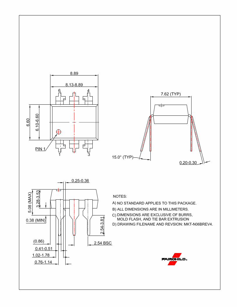
Schematic Package Outlines
Cathode 2
Anode 1
No Connection 3
5 Collector
6 Base
4 Emitter
©2005 Fairchild Semiconductor Corporation www.fairchildsemi.comMCT2M, MCT2EM, MCT210M, MCT271M Rev. 1.0.3 2
MC
T2M
, MC
T2E
M, M
CT
210M, M
CT
271M —
Ph
oto
transisto
r Op
toco
up
lers
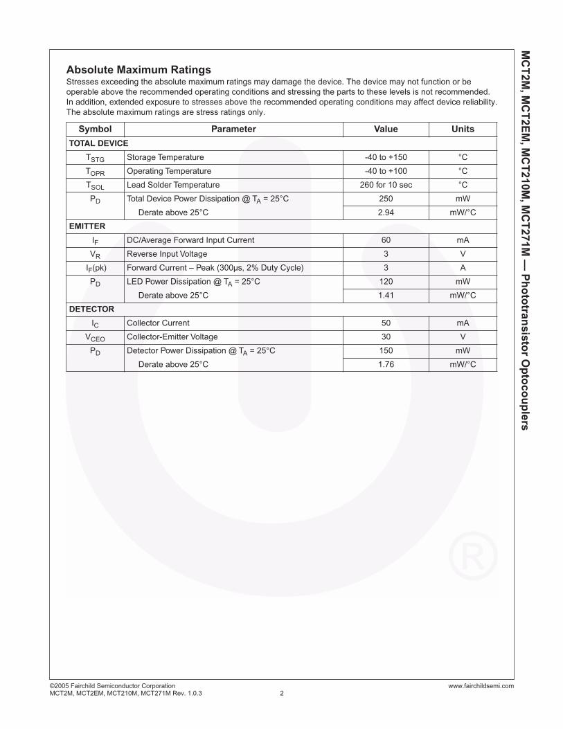
Absolute Maximum Ratings
Stresses exceeding the absolute maximum ratings may damage the device. The device may not function or be operable above the recommended operating conditions and stressing the parts to these levels is not recommended. In addition, extended exposure to stresses above the recommended operating conditions may affect device reliability.The absolute maximum ratings are stress ratings only.
Symbol Parameter Value Units
TOTAL DEVICE
T
STG
Storage Temperature -40 to +150 °C
T
OPR
Operating Temperature -40 to +100 °C
T
SOL
Lead Solder Temperature 260 for 10 sec °C
P
D
Total Device Power Dissipation @ T
A
= 25°C 250 mW
Derate above 25°C 2.94 mW/°C
EMITTER
I
F
DC/Average Forward Input Current 60 mA
V
R
Reverse Input Voltage 3 V
I
F
(pk) Forward Current – Peak (300µs, 2% Duty Cycle) 3 A
P
D
LED Power Dissipation @ T
A
= 25°C 120 mW
Derate above 25°C 1.41 mW/°C
DETECTOR
I
C
Collector Current 50 mA
V
CEO
Collector-Emitter Voltage 30 V
P
D
Detector Power Dissipation @ T
A
= 25°C 150 mW
Derate above 25°C 1.76 mW/°C

©2005 Fairchild Semiconductor Corporation www.fairchildsemi.comMCT2M, MCT2EM, MCT210M, MCT271M Rev. 1.0.3 3
MC
T2M
, MC
T2E
M, M
CT
210M, M
CT
271M —
Ph
oto
transisto
r Op
toco
up
lers
Electrical Characteristics
(T
A
= 25°C unless otherwise specified)
Individual Component Characteristics
*All typical T
A
= 25°C
Isolation Characteristics
*All typicals at T
A
= 25°C
Symbol Parameter Test Conditions Device Min. Typ.* Max. Units
EMITTER
V
F
Input Forward Voltage I
F
= 20mA MCT2MMCT2EMMCT271M
1.25 1.50 V
T
A
= 0°C–70°C, I
F
= 40mA MCT210M 1.33
I
R
Reverse Leakage Current
V
R
= 3.0V MCT2MMCT2EMMCT271M
0.001 10 µA
T
A
= 0°C–70°C, V
R
= 6.0V MCT210M
DETECTOR
BV
CEO
Collector-Emitter Breakdown Voltage
I
C
= 1.0mA, I
F
= 0 ALL 30 100 V
T
A
= 0°C–70°C MCT210M
BV
CBO
Collector-Base Breakdown Voltage
I
C
= 10µA, I
F
= 0 MCT2MMCT2EMMCT271M
70 120 V
T
A
= 0°C–70°C MCT210M 30
BV
ECO
Emitter-Collector Breakdown Voltage
I
E
= 100µA, I
F
= 0 MCT2MMCT2EMMCT271M
7 10 V
T
A
= 0°C–70°C MCT210M 6 10
I
CEO
Collector-Emitter Dark Current
V
CE
= 10V, I
F
= 0 ALL 1 50 nA
V
CE
= 5V, T
A
= 0°C–70°C 30 µA
I
CBO
Collector-Base Dark Current
V
CB
= 10V, I
F
= 0 ALL 20 nA
C
CE
Capacitance V
CE
= 0V, f = 1MHz ALL 8 pF
Symbol Parameter Test Conditions Min Typ* Max Units
V
ISO
Input-Output Isolation Voltage f = 60Hz, t = 1 sec. 7500 Vac(pk)
R
ISO
Isolation Resistance V
I-O
= 500 VDC 10
11
Ω
C
ISO
Isolation Capacitance 0.2 2 pF

©2005 Fairchild Semiconductor Corporation www.fairchildsemi.comMCT2M, MCT2EM, MCT210M, MCT271M Rev. 1.0.3 4
MC
T2M
, MC
T2E
M, M
CT
210M, M
CT
271M —
Ph
oto
transisto
r Op
toco
up
lers
Electrical Characteristics
(Continued)
(T
A
= 25°C unless otherwise specified)
Transfer Characteristics
*All typicals at T
A
= 25°C
Symbol Parameter Test Conditions Device Min. Typ.* Max. Unit
DC CHARACTERISTICS
CTR Output CollectorCurrent
T
A
= 0°C–70°C MCT210M 150 %
I
F
= 10mA, V
CE
= 10V MCT2MMCT2EM
20
MCT271M 45 90
I
F
= 3.2mA to 32mA, V
CE
= 0.4V, T
A
= 0°C–70°CMCT210M 50
V
CE(SAT)
Collector-EmitterSaturation Voltage
I
C
= 2mA, I
F
= 16mA MCT2MMCT2EMMCT271M
0.4 V
I
C
= 16mA, I
F
= 32mA, T
A
= 0°C–70°CMCT210M
AC CHARACTERISTICS
t
on
AC Characteristic Saturated Turn-on Time from 5V to 0.8V
I
F
= 15mA, V
CC
= 5V, R
L
= 2k
Ω
, R
B
= Open (Fig. 11)MCT2M
MCT2EM1.1 µs
I
F
= 20mA, V
CC
= 5 V,
R
L
= 2k
Ω
, R
B
= 100k
Ω
) (Fig. 11)
MCT2MMCT2EM
1.3
t
off
Saturated Turn-off Time from SAT to 2.0 V
I
F
= 15mA, V
CC
= 5V, R
L
= 2k
Ω
, R
B
= Open (Fig. 11)MCT2M
MCT2EM50 µs
I
F
= 20mA, V
CC
= 5V,
R
L
= 2k
Ω
, R
B
= 100k
Ω
(Fig. 11)
MCT2MMCT2EM
20
t
on
Turn-on Time I
F
= 10mA, V
CC
= 10V, R
L
= 100
Ω
MCT2MMCT2EM
2 µs
t
off
Turn-off Time I
F
= 10mA, V
CC
= 10V, R
L
= 100
Ω
MCT2MMCT2EM
2 µs
t
r
Rise Time I
F
= 10mA, V
CC = 10V, RL = 100Ω
MCT2MMCT2EM
2 µs
tf Fall Time IF = 10mA, VCC = 10V, RL = 100Ω
MCT2MMCT2EM
1.5 µs
ton Saturated turn-on time IF = 16mA, RL = 1.9kΩ, VCC = 5V (Fig. 11)
MCT271M 1.0 µs
toff Saturated turn-off time(Approximates a typical TTL interface)
48 µs
ton Saturated turn-on time IF = 16mA, RL = 4.7kΩ, VCC = 5 V (Fig. 20)
MCT271M 1.0 µs
toff Saturated turn-off time(Approximates a typical low power TTL interface)
98 µs
tr Saturated rise time IF = 16mA, RL = 560Ω, VCC = 5V) (Fig. 11, 12)
MCT210M 1.0 µs
tf Saturated fall time 11 µs
TPD (HL) Saturated propagationdelay – HIGH to LOW
IF = 16mA, RL = 2.7kΩ (Fig. 11, 12)
MCT210M 1.0 µs
TPD (LH) Saturated propagationdelay – LOW to HIGH
50 µs
tr Non-saturated rise time IC = 2mA, VCC = 5V, RL = 100Ω (Fig. 11)
MCT210M 2 µs
tf Non-saturated fall time 2 µs
ton Non-saturated turn-on time IC = 2mA, VCC = 5V, RL = 100Ω (Fig. 20)
MCT271M 2 7 µs
toff Non-saturated turn-off time 2 7 µs

©2005 Fairchild Semiconductor Corporation www.fairchildsemi.comMCT2M, MCT2EM, MCT210M, MCT271M Rev. 1.0.3 5
MC
T2M
, MC
T2E
M, M
CT
210M, M
CT
271M —
Ph
oto
transisto
r Op
toco
up
lers
Safety and Insulation RatingsAs per IEC 60747-5-2, this optocoupler is suitable for “safe electrical insulation” only within the safety limit data. Compliance with the safety ratings shall be ensured by means of protective circuits.
Symbol Parameter Min. Typ. Max. Unit
Installation Classifications per DIN VDE 0110/1.89 Table 1
For Rated Main Voltage < 150Vrms I-IV
For Rated Main voltage < 300Vrms I-IV
Climatic Classification 55/100/21
Pollution Degree (DIN VDE 0110/1.89) 2
CTI Comparative Tracking Index 175
VPR Input to Output Test Voltage, Method b, VIORM x 1.875 = VPR, 100% Production Test with tm = 1 sec, Partial Discharge < 5pC
1594 Vpeak
Input to Output Test Voltage, Method a, VIORM x 1.5 = VPR, Type and Sample Test with tm = 60 sec, Partial Discharge < 5pC
1275 Vpeak
VIORM Max. Working Insulation Voltage 850 Vpeak
VIOTM Highest Allowable Over Voltage 6000 Vpeak
External Creepage 7 mm
External Clearance 7 mm
Insulation Thickness 0.5 mm
RIO Insulation Resistance at Ts, VIO = 500V 109 Ω
©2005 Fairchild Semiconductor Corporation www.fairchildsemi.comMCT2M, MCT2EM, MCT210M, MCT271M Rev. 1.0.3 6
MC
T2M
, MC
T2E
M, M
CT
210M, M
CT
271M —
Ph
oto
transisto
r Op
toco
up
lers
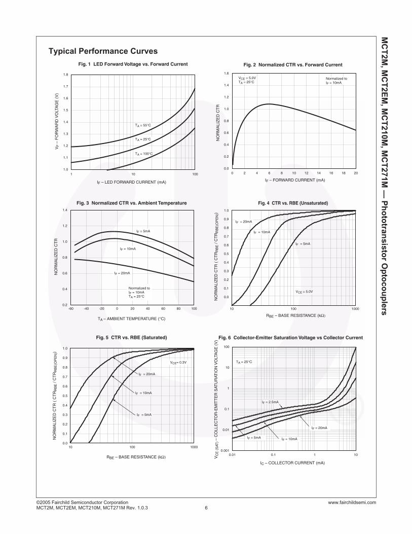
Typical Performance Curves
Fig. 2 Normalized CTR vs. Forward Current
IF – FORWARD CURRENT (mA)
0 2 4 6 8 10 12 14 16 18 20
NO
RM
ALI
ZE
D C
TR
0.0
0.2
0.4
0.6
0.8
1.0
1.2
1.4
1.6 VCE = 5.0V TA = 25°C
Normalized toIF = 10mA
Fig. 3 Normalized CTR vs. Ambient Temperature
TA – AMBIENT TEMPERATURE (°C)
-60 -40 -20 0 20 40 60 80 100
NO
RM
ALI
ZE
D C
TR
0.2
0.4
0.6
0.8
1.0
1.2
1.4
IF = 5mA
IF = 10mA
IF = 20mA
Normalized toIF = 10mA TA = 25°C
IF – LED FORWARD CURRENT (mA)
VF –
FO
RW
AR
D V
OLT
AG
E (
V)
Fig. 1 LED Forward Voltage vs. Forward Current
1 10 1001.0
1.1
1.2
1.3
1.4
1.5
1.6
1.7
1.8
TA = 25°C
TA = 55°C
TA = 100°C
Fig. 5 CTR vs. RBE (Saturated)
RBE – BASE RESISTANCE (kΩ)
NO
RM
ALI
ZE
D C
TR
( C
TR
RB
E /
CT
RR
BE
(OP
EN
))
10 100 10000.0
0.1
0.2
0.3
0.4
0.5
0.6
0.7
0.8
0.9
1.0
IF = 20mA
IF = 10mA
IF = 5mA
VCE= 0.3V
Fig. 4 CTR vs. RBE (Unsaturated)
RBE – BASE RESISTANCE (kΩ)
NO
RM
ALI
ZE
D C
TR
( C
TR
RB
E /
CT
RR
BE
(OP
EN
))
10 100 1000
0.0
0.1
0.2
0.3
0.4
0.5
0.6
0.7
0.8
0.9
1.0
VCE = 5.0V
IF = 20mA
IF = 10mA
IF = 5mA
0.01 0.1 1 100.001
0.01
0.1
1
10
100
IF = 5mA
IF = 20mA
IF = 10mA
Fig. 6 Collector-Emitter Saturation Voltage vs Collector Current
IC – COLLECTOR CURRENT (mA)
VC
E (
SAT
) – C
OLL
EC
TOR
-EM
ITT
ER
SAT
UR
ATIO
N V
OLT
AG
E (
V)
IF = 2.5mA
TA = 25°C

©2005 Fairchild Semiconductor Corporation www.fairchildsemi.comMCT2M, MCT2EM, MCT210M, MCT271M Rev. 1.0.3 7
MC
T2M
, MC
T2E
M, M
CT
210M, M
CT
271M —
Ph
oto
transisto
r Op
toco
up
lers
Typical Performance Curves (Continued)
NO
RM
ALI
ZE
D t o
n –
(ton
(RB
E) /
t on(
open
))
Fig. 8 Normalized ton vs. RBE
RBE – BASE RESISTANCE (kΩ)
10 100 1000 10000 100000
0.5
1.0
1.5
2.0
2.5
3.0
3.5
4.0
4.5
5.0
VCC = 10VIC = 2mARL = 100Ω
SW
ITC
HIN
G S
PE
ED
(µs
)
Fig. 7 Switching Speed vs. Load Resistor
R – LOAD RESISTOR (kΩ)
0.1 1 10 100
0.1
1
10
100
1000
Toff
IF = 10mA VCC = 10VTA = 25°C
Tr
Ton
Tf
0.1
0.2
0.3
0.4
0.5
0.6
0.7
0.8
0.9
1.0
1.1
1.2
1.3
1.4
VCC = 10VIC = 2mARL = 100Ω
NO
RM
ALI
ZE
D t o
ff –
(tof
f(R
BE
) / t o
ff(op
en))
10 100 1000 10000 100000
RBE – BASE RESISTANCE (kΩ)
Fig. 9 Normalized toff vs. RBEFig. 10 Dark Current vs. Ambient Temperature
TA – AMBIENT TEMPERATURE (˚C)
0 20 40 60 80 100
I CE
O -
CO
LLE
CTO
R -E
MIT
TER
DA
RK
CU
RR
EN
T (n
A)
0.001
0.01
0.1
1
10
100
1000
10000
VCE = 10 VTA = 25˚C
©2005 Fairchild Semiconductor Corporation www.fairchildsemi.comMCT2M, MCT2EM, MCT210M, MCT271M Rev. 1.0.3 8
MC
T2M
, MC
T2E
M, M
CT
210M, M
CT
271M —
Ph
oto
transisto
r Op
toco
up
lers
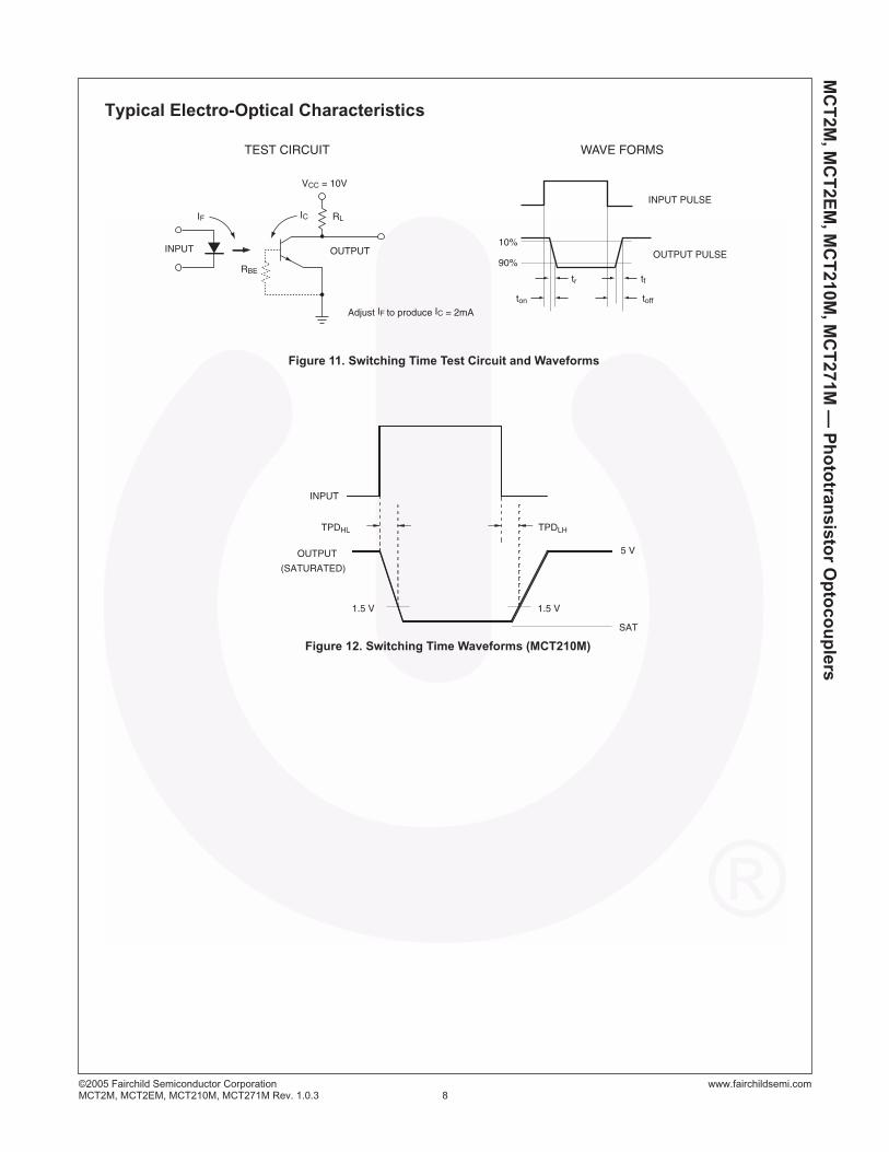
Typical Electro-Optical Characteristics
OUTPUT PULSE
INPUT PULSE
TEST CIRCUIT WAVE FORMS
tr tf
INPUT
IF RL
RBE
VCC = 10V
OUTPUT
ton
10%
90%
toff
Figure 11. Switching Time Test Circuit and Waveforms
Figure 12. Switching Time Waveforms (MCT210M)
IC
Adjust IF to produce IC = 2mA
OUTPUT
(SATURATED)
INPUT
5 V
1.5 V
TPDHL TPDLH
1.5 V
SAT

©2005 Fairchild Semiconductor Corporation www.fairchildsemi.comMCT2M, MCT2EM, MCT210M, MCT271M Rev. 1.0.3 9
MC
T2M
, MC
T2E
M, M
CT
210M, M
CT
271M —
Ph
oto
transisto
r Op
toco
up
lers
Ordering Information
Marking Information
OptionOrder Entry Identifier
(Example) Description
No suffix MCT2M Standard Through Hole Device (50 units per tube)
S MCT2SM Surface Mount Lead Bend
SR2 MCT2SR2M Surface Mount; Tape and Reel (1,000 units per reel)
T MCT2TM 0.4" Lead Spacing
V MCT2VM IEC60747-5-2
TV MCT2TVM IEC60747-5-2, 0.4" Lead Spacing
SV MCT2SVM IEC60747-5-2, Surface Mount
SR2V MCT2SR2VM IEC60747-5-2, Surface Mount, Tape and Reel (1,000 units per reel)
*Note – Parts that do not have the ‘V’ option (see definition 3 above) that are marked with date code ‘325’ or earlier are marked in portrait format.
Definitions
1 Fairchild logo
2 Device number
3 VDE mark (Note: Only appears on parts ordered with VDE option – See order entry table)
4 One digit year code, e.g., ‘7’
5 Two digit work week ranging from ‘01’ to ‘53’
6 Assembly package code
MCT2
V X YY Q
1
2
6
43 5
©2005 Fairchild Semiconductor Corporation www.fairchildsemi.comMCT2M, MCT2EM, MCT210M, MCT271M Rev. 1.0.3 10
MC
T2M
, MC
T2E
M, M
CT
210M, M
CT
271M —
Ph
oto
transisto
r Op
toco
up
lers
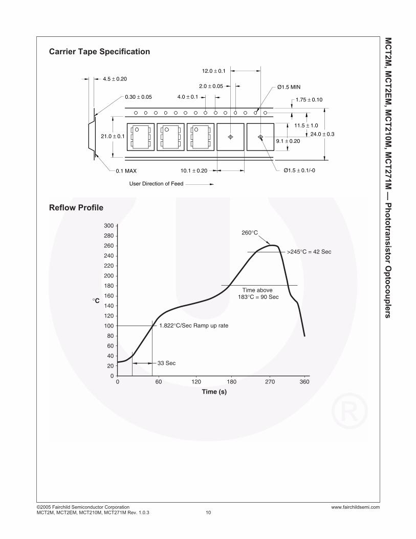
Carrier Tape Specification
Reflow Profile
4.0 ± 0.1
Ø1.5 MIN
User Direction of Feed
2.0 ± 0.05
1.75 ± 0.10
11.5 ± 1.0
24.0 ± 0.3
12.0 ± 0.1
0.30 ± 0.05
21.0 ± 0.1
4.5 ± 0.20
0.1 MAX 10.1 ± 0.20
9.1 ± 0.20
Ø1.5 ± 0.1/-0
300
280
260
240
220
200
180
160
140
120
100
80
60
40
20
0
°C
Time (s)
0 60 180120 270
260°C
>245°C = 42 Sec
Time above 183°C = 90 Sec
360
1.822°C/Sec Ramp up rate
33 Sec


www.onsemi.com1
ON Semiconductor and are trademarks of Semiconductor Components Industries, LLC dba ON Semiconductor or its subsidiaries in the United States and/or other countries.ON Semiconductor owns the rights to a number of patents, trademarks, copyrights, trade secrets, and other intellectual property. A listing of ON Semiconductor’s product/patentcoverage may be accessed at www.onsemi.com/site/pdf/Patent−Marking.pdf. ON Semiconductor reserves the right to make changes without further notice to any products herein.ON Semiconductor makes no warranty, representation or guarantee regarding the suitability of its products for any particular purpose, nor does ON Semiconductor assume any liabilityarising out of the application or use of any product or circuit, and specifically disclaims any and all liability, including without limitation special, consequential or incidental damages.Buyer is responsible for its products and applications using ON Semiconductor products, including compliance with all laws, regulations and safety requirements or standards,regardless of any support or applications information provided by ON Semiconductor. “Typical” parameters which may be provided in ON Semiconductor data sheets and/orspecifications can and do vary in different applications and actual performance may vary over time. All operating parameters, including “Typicals” must be validated for each customerapplication by customer’s technical experts. ON Semiconductor does not convey any license under its patent rights nor the rights of others. ON Semiconductor products are notdesigned, intended, or authorized for use as a critical component in life support systems or any FDA Class 3 medical devices or medical devices with a same or similar classificationin a foreign jurisdiction or any devices intended for implantation in the human body. Should Buyer purchase or use ON Semiconductor products for any such unintended or unauthorizedapplication, Buyer shall indemnify and hold ON Semiconductor and its officers, employees, subsidiaries, affiliates, and distributors harmless against all claims, costs, damages, andexpenses, and reasonable attorney fees arising out of, directly or indirectly, any claim of personal injury or death associated with such unintended or unauthorized use, even if suchclaim alleges that ON Semiconductor was negligent regarding the design or manufacture of the part. ON Semiconductor is an Equal Opportunity/Affirmative Action Employer. Thisliterature is subject to all applicable copyright laws and is not for resale in any manner.
PUBLICATION ORDERING INFORMATIONN. American Technical Support: 800−282−9855 Toll FreeUSA/Canada
Europe, Middle East and Africa Technical Support:Phone: 421 33 790 2910
Japan Customer Focus CenterPhone: 81−3−5817−1050
www.onsemi.com
LITERATURE FULFILLMENT:Literature Distribution Center for ON Semiconductor19521 E. 32nd Pkwy, Aurora, Colorado 80011 USAPhone: 303−675−2175 or 800−344−3860 Toll Free USA/CanadaFax: 303−675−2176 or 800−344−3867 Toll Free USA/CanadaEmail: [email protected]
ON Semiconductor Website: www.onsemi.com
Order Literature: http://www.onsemi.com/orderlit
For additional information, please contact your localSales Representative
© Semiconductor Components Industries, LLC