1 5. impedance matching and tuning apply the theory and techniques of the previous chapters to...
TRANSCRIPT
1
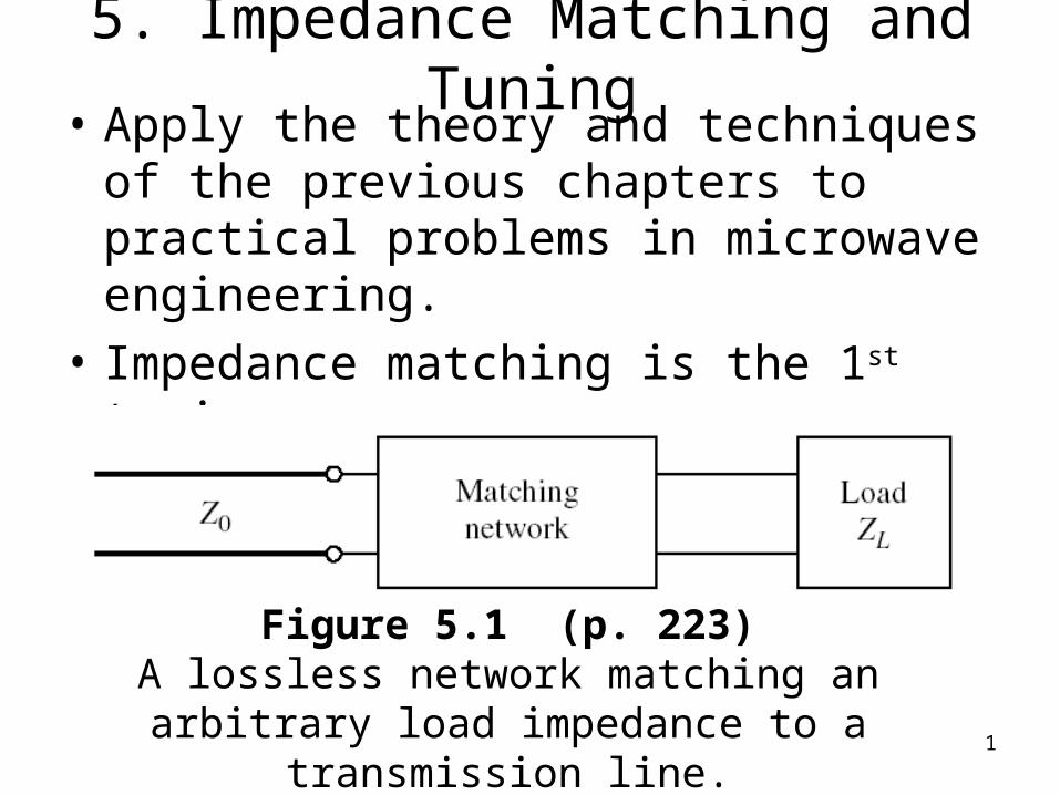
5. Impedance Matching and Tuning• Apply the theory and techniques of the
previous chapters to practical problems in microwave engineering.
• Impedance matching is the 1st topic.
Figure 5.1 (p. 223)A lossless network matching an arbitrary load
impedance to a transmission line.

2
• Impedance matching or tuning is important since– Maximum power is delivered when the load is
matched to the line, and power loss in the feed line is minimized.
– Impedance matching sensitive receiver components improves the signal-to-noise ratio of the system.
– Impedance matching in a power distribution network will reduce the amplitude and phase errors.
3
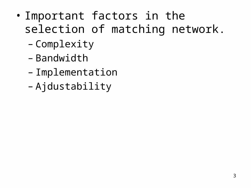
• Important factors in the selection of matching network.– Complexity– Bandwidth– Implementation– Ajdustability
4
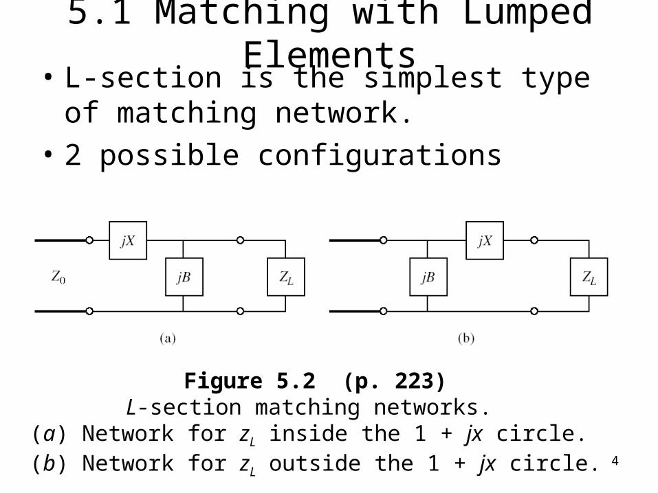
5.1 Matching with Lumped Elements• L-section is the simplest type of matching
network.
• 2 possible configurations
Figure 5.2 (p. 223)L-section matching networks.
(a) Network for zL inside the 1 + jx circle. (b) Network for zL outside the 1 + jx circle.
5
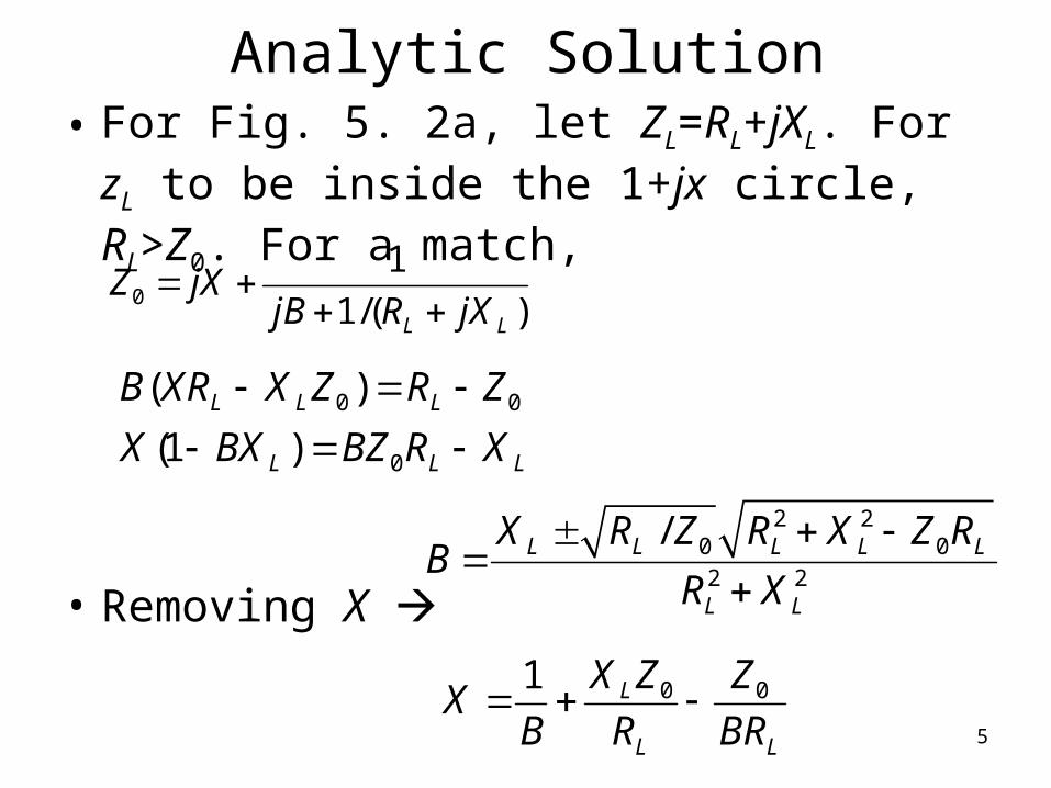
Analytic Solution• For Fig. 5. 2a, let ZL=RL+jXL. For zL to be
inside the 1+jx circle, RL>Z0. For a match,
• Removing X
0
1
1/( )L L
Z jXjB R jX
0 0
0
( )
(1 )L L L
L L L
B XR X Z R Z
X BX BZ R X
2 20 02 2
/L L L L L
L L
X R Z R X Z RB
R X
0 01 L
L L
X Z ZX
B R BR
6
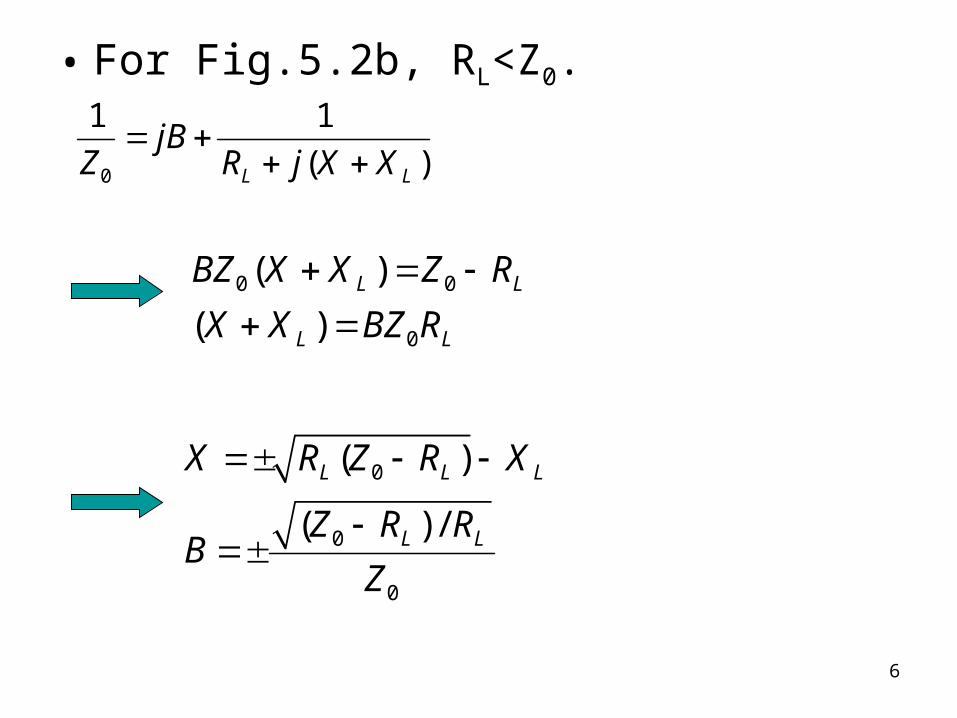
• For Fig.5.2b, RL<Z0.
0
1 1
( )L L
jBZ R j X X
0 0
0
( )
( )L L
L L
BZ X X Z R
X X BZ R
0
0
0
( )
( ) /
L L L
L L
X R Z R X
Z R RB
Z
7
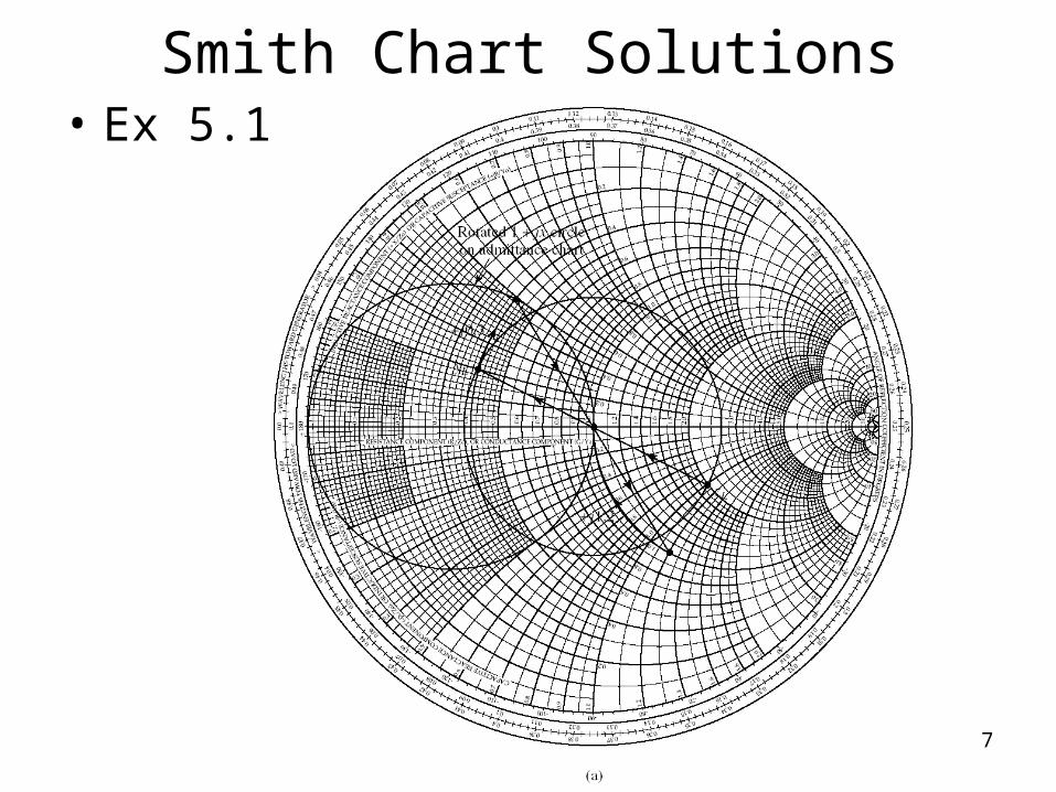
Smith Chart Solutions• Ex 5.1
8
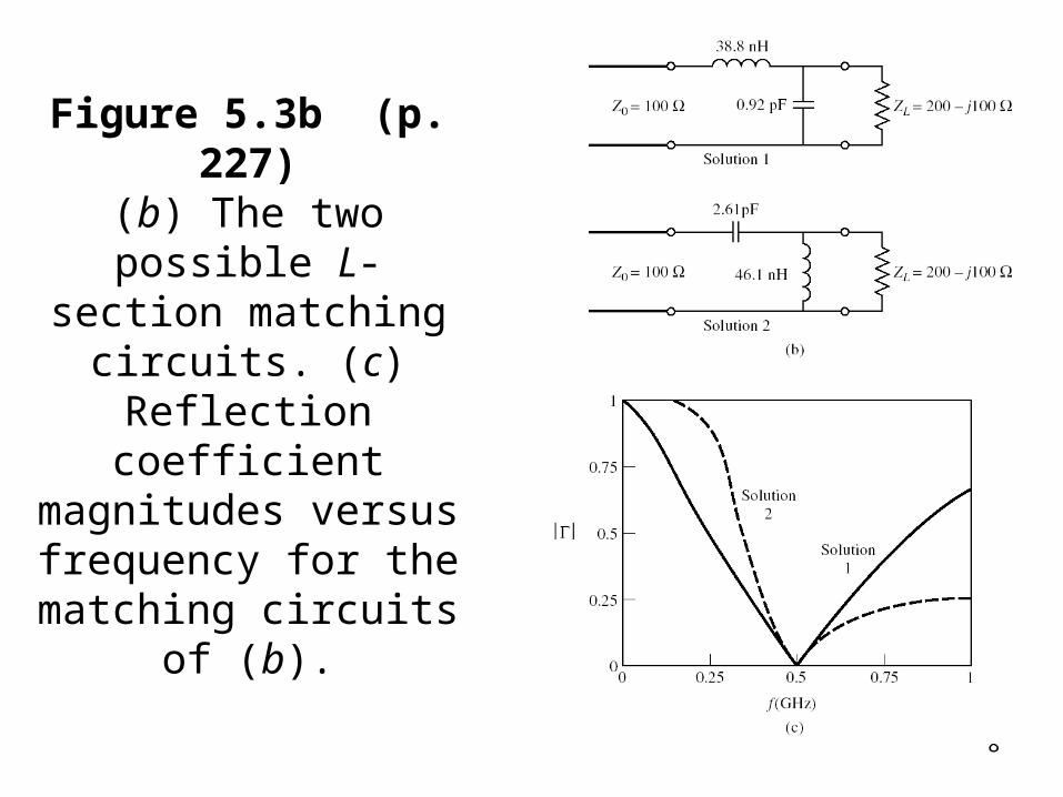
Figure 5.3b (p. 227)(b) The two possible L-
section matching circuits. (c) Reflection coefficient magnitudes
versus frequency for the matching circuits of (b).
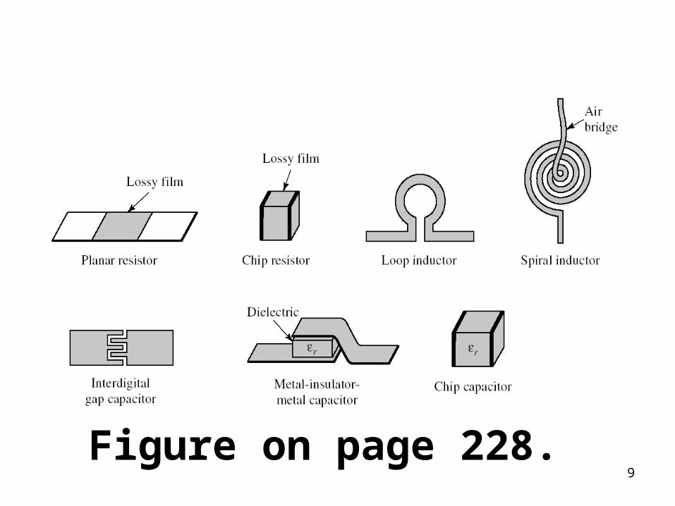
9Figure on page 228.
10
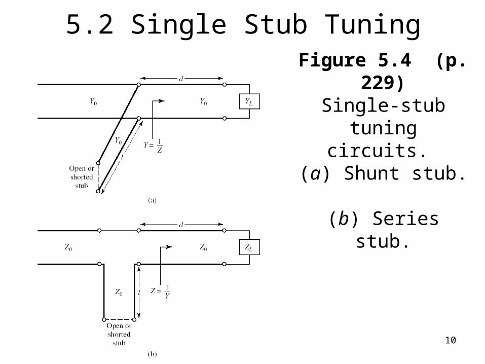
5.2 Single Stub Tuning
Figure 5.4 (p. 229)Single-stub tuning
circuits. (a) Shunt stub. (b) Series stub.

11
• 2 adjustable parameters– d: from the load to the stub position.– B or X provided by the shunt or series stub.
• For the shunt-stub case, – Select d so that Y seen looking into the line at d
from the load is Y0+jB
– Then the stub susceptance is chosen as –jB.
• For the series-stub case,– Select d so that Z seen looking into the line at d
from the load is Z0+jX
– Then the stub reactance is chosen as –jX.
12
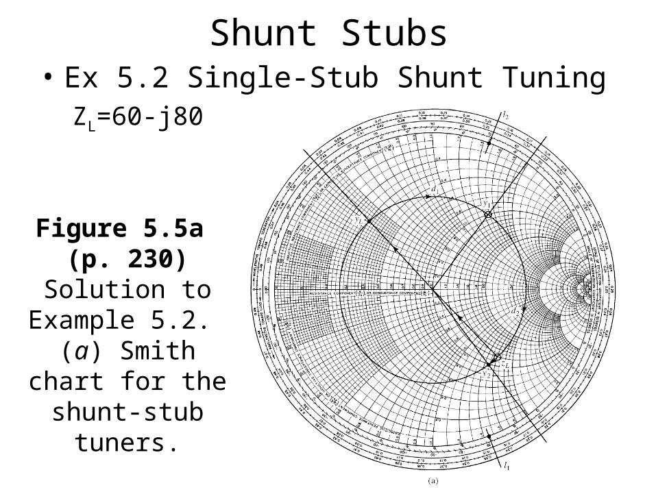
Shunt Stubs• Ex 5.2 Single-Stub Shunt Tuning
ZL=60-j80
Figure 5.5a (p. 230)
Solution to Example 5.2.
(a) Smith chart for the shunt-stub
tuners.
13
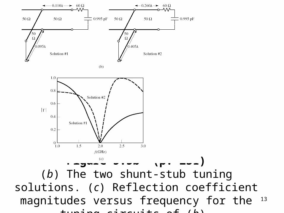
Figure 5.5b (p. 231)(b) The two shunt-stub tuning solutions. (c) Reflection coefficient magnitudes versus frequency for the tuning
circuits of (b).
14
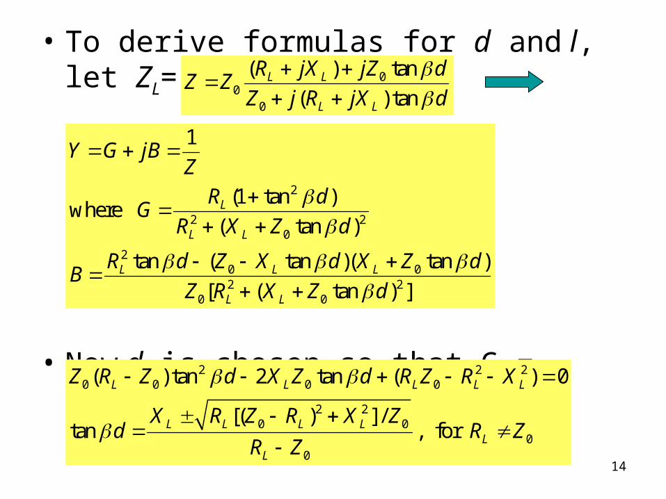
• To derive formulas for d and l, let ZL= 1/YL= RL+ jXL.
• Now d is chosen so that G = Y0=1/Z0,
00
0
( ) tan
( ) tanL L
L L
R jX jZ dZ Z
Z j R jX d
2
2 20
20 02 2
0 0
1
(1 tan )where
( tan )
tan ( tan )( tan )
[ ( tan ) ]
L
L L
L L L
L L
Y G jBZ
R dG
R X Z d
R d Z X d X Z dB
Z R X Z d
2 2 20 0 0 0
2 20 0
00
( ) tan 2 tan ( ) 0
[( ) ] /tan , for
L L L L L
L L L LL
L
Z R Z d X Z d R Z R X
X R Z R X Zd R Z
R Z
15
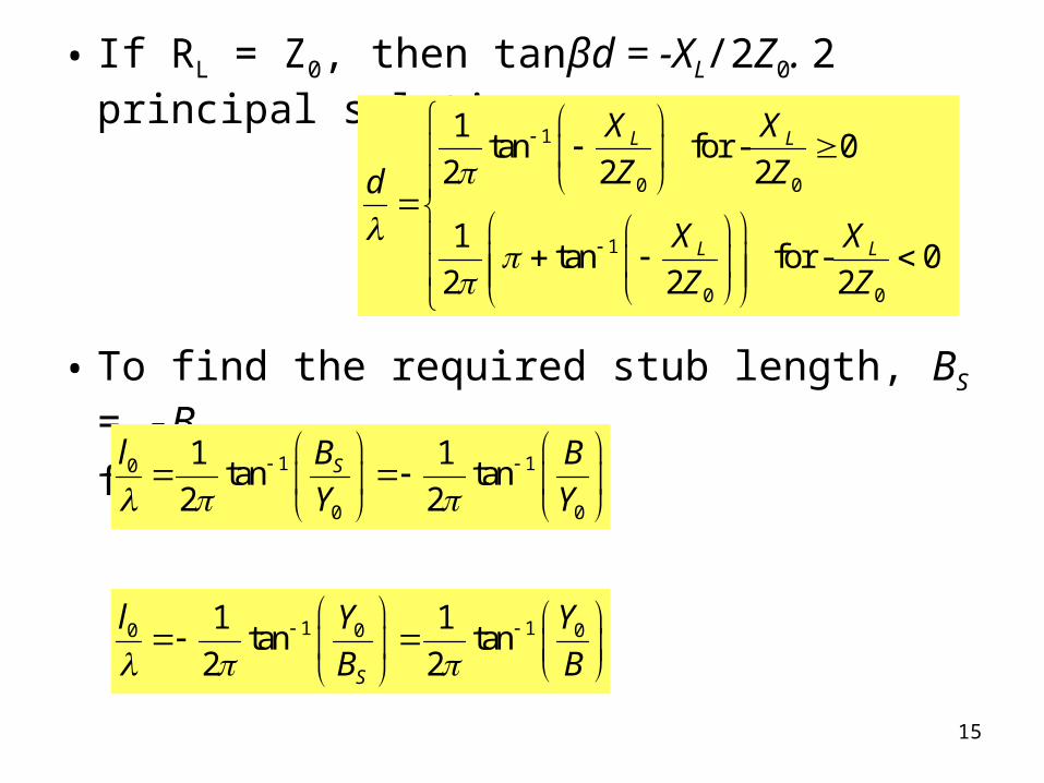
• If RL = Z0, then tanβd = -XL/2Z0. 2 principal solutions are
• To find the required stub length, BS = -B.
for open stub
for short stub
1
0 0
1
0 0
1tan for - 0
2 2 2
1tan for - 0
2 2 2
L L
L L
X X
Z Zd
X X
Z Z
1 10
0 0
1 1tan tan
2 2Sl B B
Y Y
1 10 0 01 1tan tan
2 2S
l Y Y
B B
16
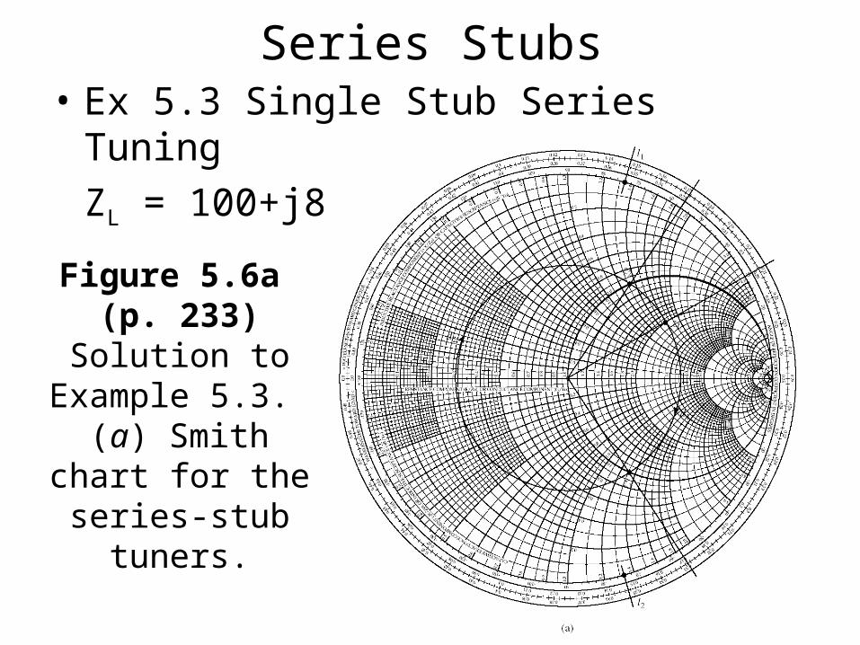
Series Stubs• Ex 5.3 Single Stub Series Tuning
ZL = 100+j80
Figure 5.6a (p. 233)Solution to Example
5.3. (a) Smith chart for
the series-stub tuners.
17
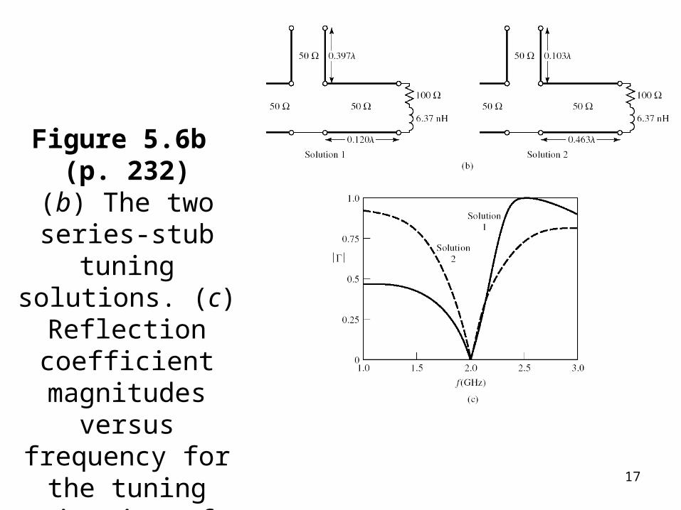
Figure 5.6b (p. 232)(b) The two series-
stub tuning solutions. (c) Reflection
coefficient magnitudes versus frequency for the
tuning circuits of (b).
18
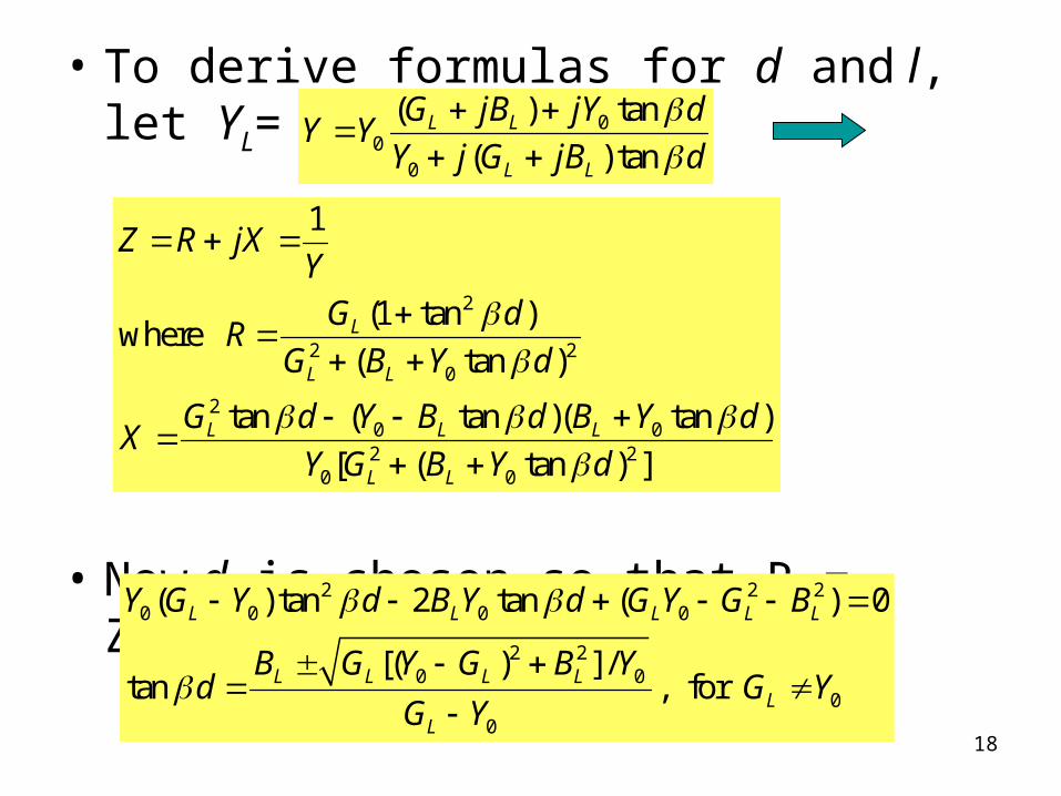
• To derive formulas for d and l, let YL= 1/ZL= GL+ jBL.
• Now d is chosen so that R = Z0=1/Y0,
00
0
( ) tan
( ) tanL L
L L
G jB jY dY Y
Y j G jB d
2
2 20
20 02 2
0 0
1
(1 tan )where
( tan )
tan ( tan )( tan )
[ ( tan ) ]
L
L L
L L L
L L
Z R jXY
G dR
G B Y d
G d Y B d B Y dX
Y G B Y d
2 2 20 0 0 0
2 20 0
00
( ) tan 2 tan ( ) 0
[( ) ] /tan , for
L L L L L
L L L LL
L
Y G Y d B Y d G Y G B
B G Y G B Yd G Y
G Y

19
• If GL = Y0, then tanβd = -BL/2Y0. 2 principal solutions are
• To find the required stub length, XS = -X.
for short stub
for open stub
1
0 0
1
0 0
1tan for - 0
2 2 2
1tan for - 0
2 2 2
L L
L L
B B
Y Yd
B B
Y Y
1 10
0 0
1 1tan tan
2 2Sl X X
Z Z
1 10 0 01 1tan tan
2 2S
l Z Z
X X
20
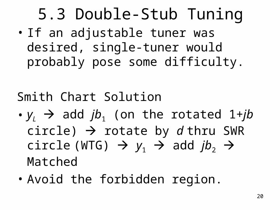
5.3 Double-Stub Tuning• If an adjustable tuner was desired, single-tuner
would probably pose some difficulty.
Smith Chart Solution
• yL add jb1 (on the rotated 1+jb circle) rotate by d thru SWR circle (WTG) y1 add jb2 Matched
• Avoid the forbidden region.
21
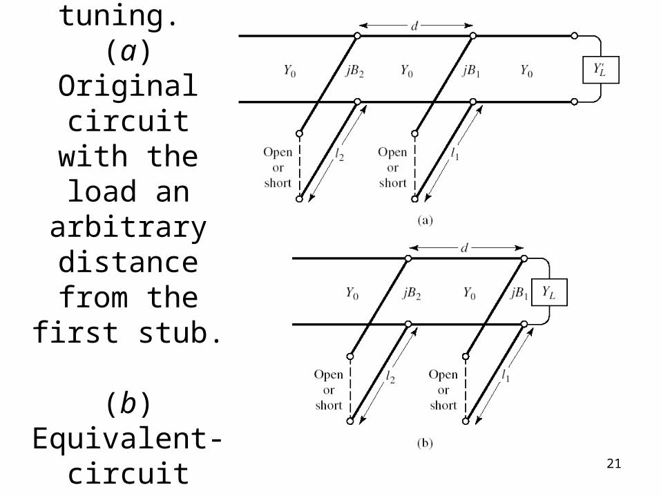
Figure 5.7 (p. 236)
Double-stub tuning.
(a) Original circuit with the
load an arbitrary distance from the
first stub. (b) Equivalent-circuit with load at the first stub.
22
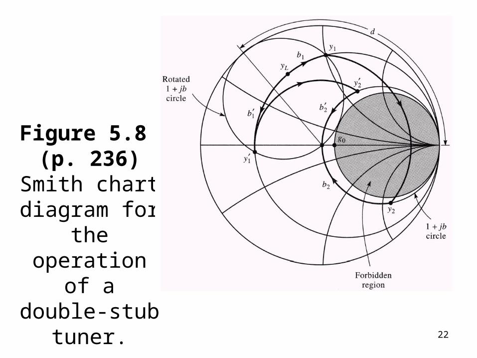
Figure 5.8 (p. 236)
Smith chart diagram for the operation of a double-stub
tuner.

23
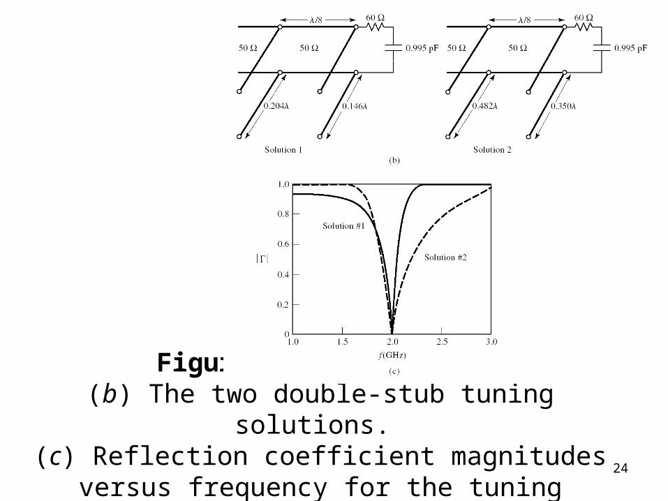
Figure 5.9a (p. 238)
Solution to Example 5.4. (a) Smith chart for the double-
stub tuners.
Ex. 5.4 ZL = 60-j80
Open stubs, d = λ/8
24
Figure 5.9b (p. 239)(b) The two double-stub tuning solutions.
(c) Reflection coefficient magnitudes versus frequency for the tuning circuits of (b).
25
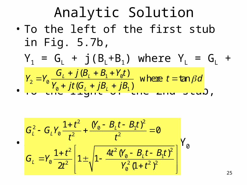
Analytic Solution• To the left of the first stub in Fig. 5.7b,
Y1 = GL + j(BL+B1) where YL = GL + jBL
• To the right of the 2nd stub,
• At this point, Re{Y2} = Y0
1 02 0
0 1
( ) where tan
( )L L
L L
G j B B Y tY Y t d
Y jt G jB jB
222 0 1
0 2 2
2 220 1
0 2 2 2 20
( )10
4 ( )11 1
2 (1 )
LL L
LL
Y B t B ttG G Y
t t
t Y B t B ttG Y
t Y t

26
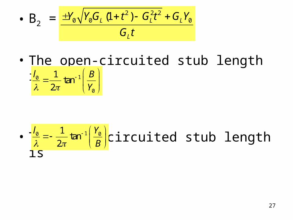
• Since GL is real,
• After d has been fixed, the 1st stub susceptance can be determined as
• The 2nd stub susceptance can be found from the negative of the imaginary part of (5.18)
2 20 12 2 2
0
4 ( )0 1
(1 )Lt Y B t B t
Y t
2
00 2 2
10
sinL
YtG Y
t d
2 2 20 0
1
(1 ) L LL
Y t G Y G tB B
t
27
• B2 =
• The open-circuited stub length is
• The short-circuited stub length is
2 2 20 0 0(1 )L L L
L
Y Y G t G t G Y
G t
10
0
1tan
2
l B
Y
10 01tan
2
l Y
B
28
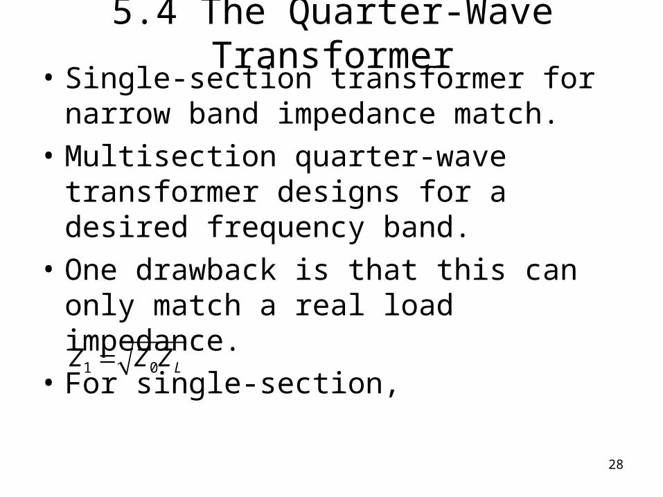
5.4 The Quarter-Wave Transformer• Single-section transformer for narrow band
impedance match.
• Multisection quarter-wave transformer designs for a desired frequency band.
• One drawback is that this can only match a real load impedance.
• For single-section,
1 0 LZ Z Z

29
Figure 5.10 (p. 241)A single-section quarter-wave matching
transformer. at the design frequency f0.
40

30
• The input impedance seen looking into the matching section is
where t = tanβl = tanθ, θ = π/2 at f0.
• The reflection coefficient
• Since Z12 = Z0ZL,
11
1
Lin
L
Z jZ tZ Z
Z jZ t
20 1 0 1 0
20 1 0 1 0
( ) ( )
( ) ( )in L L
in L L
Z Z Z Z Z jt Z Z Z
Z Z Z Z Z jt Z Z Z
0
0 02L
L L
Z Z
Z Z j t Z Z
31
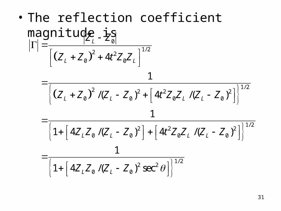
• The reflection coefficient magnitude is
01/ 22 2
0 0
1/ 22 2 2 20 0 0 0
1/ 22 2 2
0 0 0 0
1/ 22 2
0 0
4
1
/( ) 4 /( )
1
1 4 /( ) 4 /( )
1
1 4 /( ) sec
L
L L
L L L L
L L L L
L L
Z Z
Z Z t Z Z
Z Z Z Z t Z Z Z Z
Z Z Z Z t Z Z Z Z
Z Z Z Z

32
• Now assume f ≈ f0, then l ≈ λ0/4 and θ ≈ π/2. Then sec2 θ >> 1.
0
0
cos , for near / 22
L
L
Z Z
Z Z
33
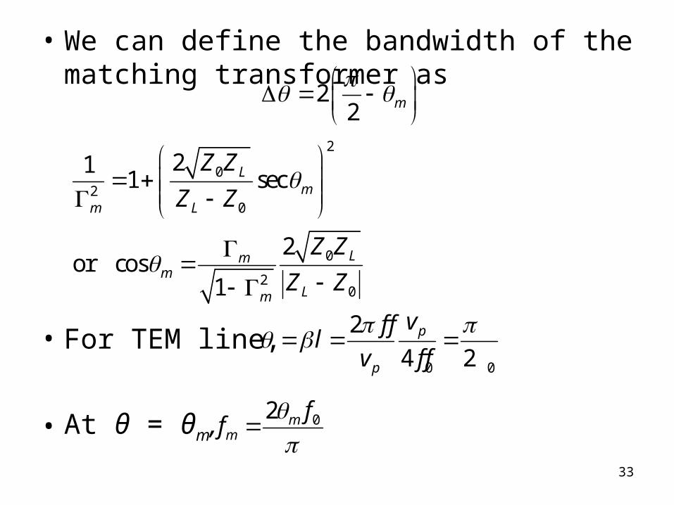
• We can define the bandwidth of the matching transformer as
• For TEM line,
• At θ = θm,
22 m
2
02
0
0
20
211 sec
2or cos
1
Lm
m L
Lmm
Lm
Z Z
Z Z
Z Z
Z Z
0 0
2
4 2p
p
vf fl
v f f
02 mm
ff
34
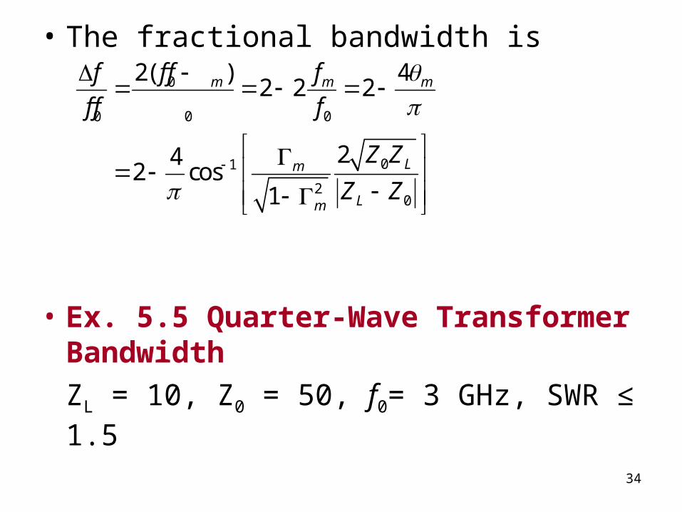
• The fractional bandwidth is
• Ex. 5.5 Quarter-Wave Transformer Bandwidth
ZL = 10, Z0 = 50, f0= 3 GHz, SWR ≤ 1.5
0
0 0 0
01
20
2( ) 42 2 2
242 cos
1
m m m
Lm
Lm
f f ff
f f f
Z Z
Z Z

35
Figure 5.12 (p. 243)Reflection coefficient magnitude versus frequency for a single-section quarter-wave matching transformer with
various load mismatches.
36
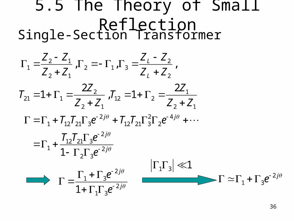
5.5 The Theory of Small ReflectionSingle-Section Transformer
2 1 21 2 1 3
2 1 2
2 121 1 12 2
2 1 2 1
2 2 41 12 21 3 12 21 3 2
212 21 3
1 22 3
, , ,
2 21 , 1
1
L
L
j j
j
j
Z Z Z Z
Z Z Z Z
Z ZT T
Z Z Z Z
T T e T T e
T T e
e
21 3
21 31
j
j
e
e
1 3 1 2
1 3je

37
Figure 5.13 (p. 244)Partial reflections and transmissions on a single-section
matching transformer.
38
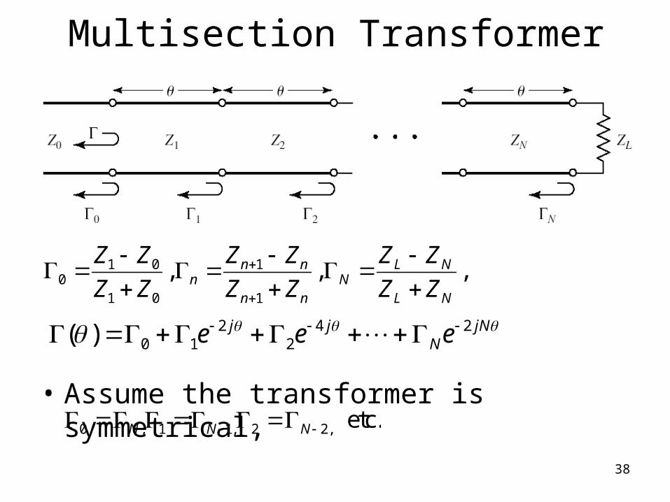
Multisection Transformer
• Assume the transformer is symmetrical,
1 0 10
1 0 1
, , ,n n L Nn N
n n L N
Z Z Z Z Z Z
Z Z Z Z Z Z
2 4 2
0 1 2( ) j j jNNe e e
0 , 1 1, 2 2, etc.N N N
39
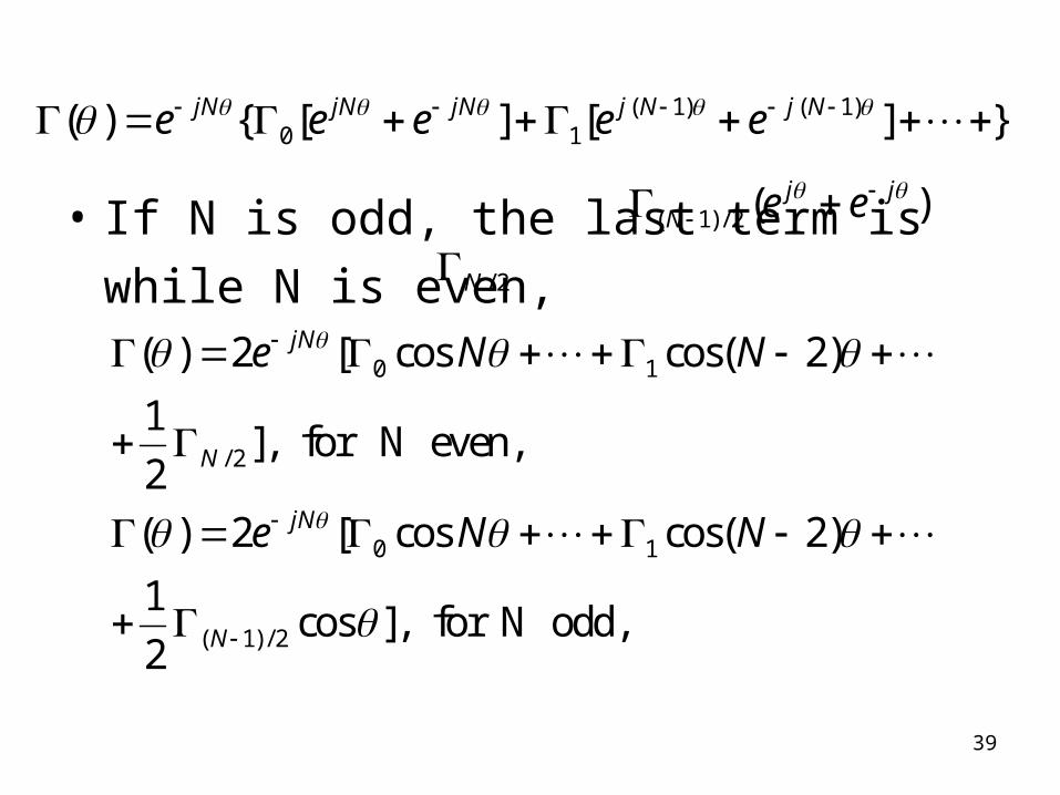
• If N is odd, the last term is
while N is even,
( 1) ( 1)0 1( ) { [ ] [ ] }jN jN jN j N j Ne e e e e
( 1) / 2 ( )j jN e e
/ 2N
0 1
/ 2
0 1
( 1) / 2
( ) 2 [ cos cos( 2)
1], for N even,
2
( ) 2 [ cos cos( 2)
1cos ], for N odd,
2
jN
N
jN
N
e N N
e N N
40
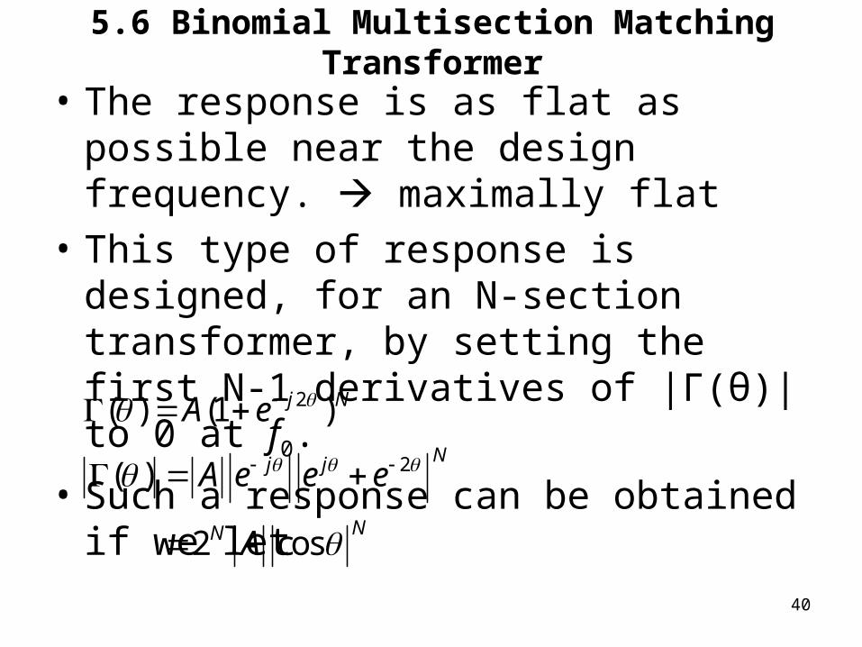
5.6 Binomial Multisection Matching Transformer
• The response is as flat as possible near the design frequency. maximally flat
• This type of response is designed, for an N-section transformer, by setting the first N-1 derivatives of |Γ(θ)| to 0 at f0.
• Such a response can be obtained if we let2( ) (1 )j NA e
2( )
2 cos
Nj j
NN
A e e e
A

41
• Note that |Γ(θ)| = 0 for θ=π/2, (dn |Γ(θ)|/dθn ) = 0 at θ=π/2 for n = 1, 2, …, N-1.
• By letting f 0,
0
0
(0) 2N L
L
Z ZA
Z Z
0
0
2 N L
L
Z ZA
Z Z
2 2
0
( ) (1 ) ,
!where
( )! !
Nj N N jn
nn
Nn
A e A C e
NC
N n n
2 2 4 20 1 2
0
( )N
N jn j j jNn N
n
A C e e e e

42
• Γn must be chosen as
• Since we assumed that Γn are small, ln x ≈ 2(x-1)/(x+1),
• Numerically solve for the characteristic impedance Table 5.1
Nn nAC
1 1
1
1 0
0 0
1ln
2
ln 2 2 2(2 ) 2 ln
n n nn
n n n
N N N N Nn L Ln n n n
n L
Z Z Z
Z Z Z
Z Z Z ZAC C C
Z Z Z Z
43
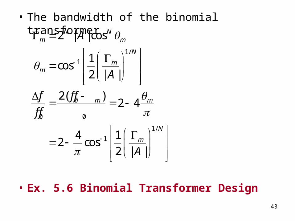
• The bandwidth of the binomial transformer
• Ex. 5.6 Binomial Transformer Design
1/
1
0
0 0
1/
1
2 | | cos
1cos
2 | |
2( )2 4
4 12 cos
2 | |
N Nm m
N
mm
m m
N
m
A
A
f ff
f f
A
44
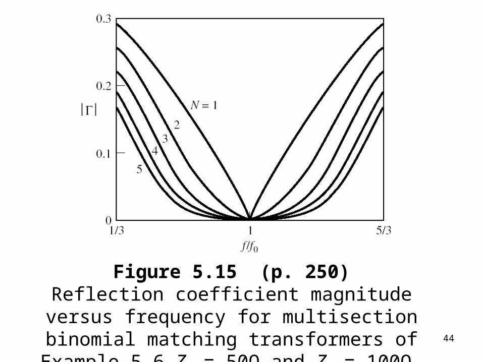
Figure 5.15 (p. 250)Reflection coefficient magnitude versus frequency for
multisection binomial matching transformers of Example 5.6 ZL = 50Ω and Z0 = 100Ω.
45
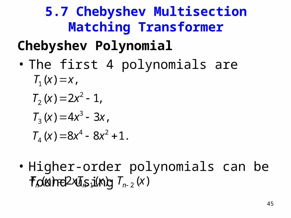
5.7 Chebyshev Multisection Matching Transformer
Chebyshev Polynomial
• The first 4 polynomials are
• Higher-order polynomials can be found using
1
22
33
4 24
( ) ,
( ) 2 1,
( ) 4 3 ,
( ) 8 8 1.
T x x
T x x
T x x x
T x x x
1 2( ) 2 ( ) ( )n n nT x xT x T x

46
Figure 5.16 (p. 251)The first four Chebyshev polynomials Tn(x).
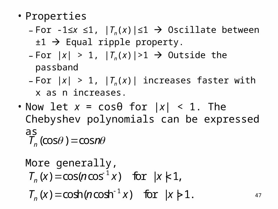
47
• Properties– For -1≤x ≤1, |Tn(x)|≤1 Oscillate between ±1
Equal ripple property.
– For |x| > 1, |Tn(x)|>1 Outside the passband
– For |x| > 1, |Tn(x)| increases faster with x as n increases.
• Now let x = cosθ for |x| < 1. The Chebyshev polynomials can be expressed as
More generally,
(cos ) cosnT n
1
1
( ) cos( cos ) for | | 1,
( ) cosh( cosh ) for | | 1.
n
n
T x n x x
T x n x x

48
• We need to map θm to x=1 and π- θm to x = -1. For this,
• Therefore,
1cos cos( ) cos (sec cos ) cos coscos cosn m
m m
T n n
1
22
33
44
2
(sec cos ) sec cos ,
(sec cos ) sec (1 2cos ) 1,
(sec cos ) sec (cos3 3cos ) 3sec cos ,
(sec cos ) sec (cos 4 4cos 2 3)
4sec (cos 2 1) 1.
m m
m m
m m m
m m
m
T
T
T
T
49
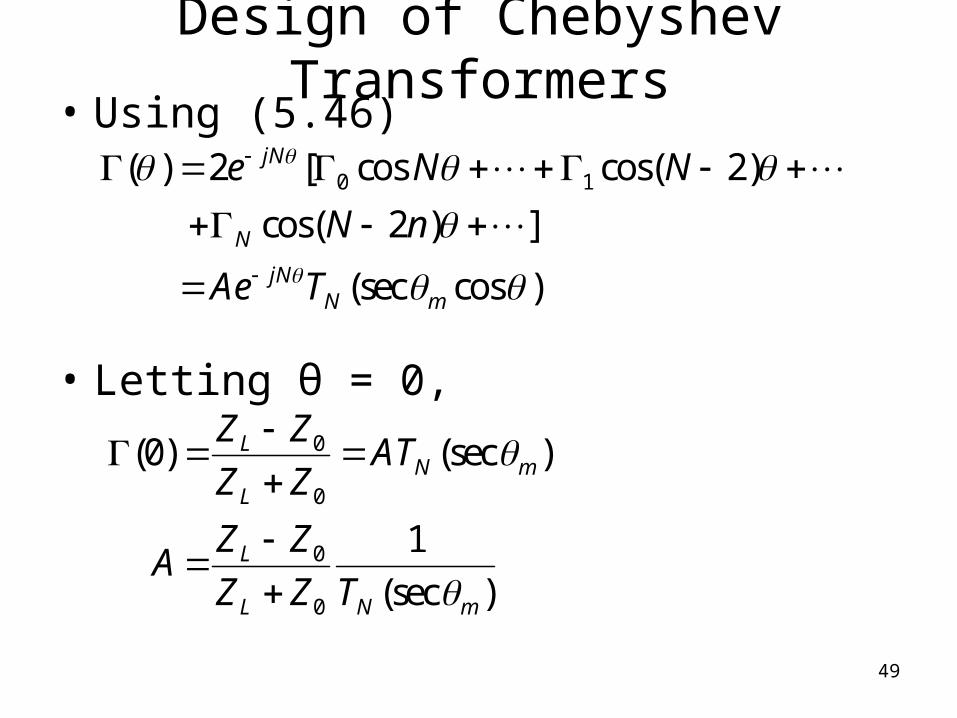
Design of Chebyshev Transformers• Using (5.46)
• Letting θ = 0,
0 1( ) 2 [ cos cos( 2)
cos( 2 ) ]
(sec cos )
jN
N
jNN m
e N N
N n
Ae T
0
0
0
0
(0) (sec )
1
(sec )
LN m
L
L
L N m
Z ZAT
Z Z
Z ZA
Z Z T

50
• If the maximum allowable reflection coefficient magnitude in the passband is Γm,
0 0
0 0 0
1
1 0
0
1
0
1 1 1(sec ) ln
2
cosh( cosh (sec ))
1 1sec cosh cosh
1 1cosh cosh ln
2
L L LN m
L m L m
m
Lm
m L
L
m
Z Z Z Z ZT
A Z Z Z Z Z
N
Z Z
N Z Z
Z
N Z

51
• Once θm is known,
Ex 5.7 Chebyshev Transformer Design
Γm = 0.05, Z0 = 50, ZL = 100
Use Table 5.2
0
2 4 mf
f

52
Figure 5.17 (p. 255)Reflection coefficient magnitude versus frequency for
the multisection matching transformers of Example 5.7.

53
Figure 5.18 (p. 256)A tapered transmission line matching
section and the model for an incremental length of tapered line. (a) The tapered transmission line matching section.
(b) Model for an incremental step change in impedance of the tapered line.

54
Figure 5.19 (p. 257)A matching section with an exponential
impedance taper. (a) Variation of impedance. (b) Resulting reflection
coefficient magnitude response.
55
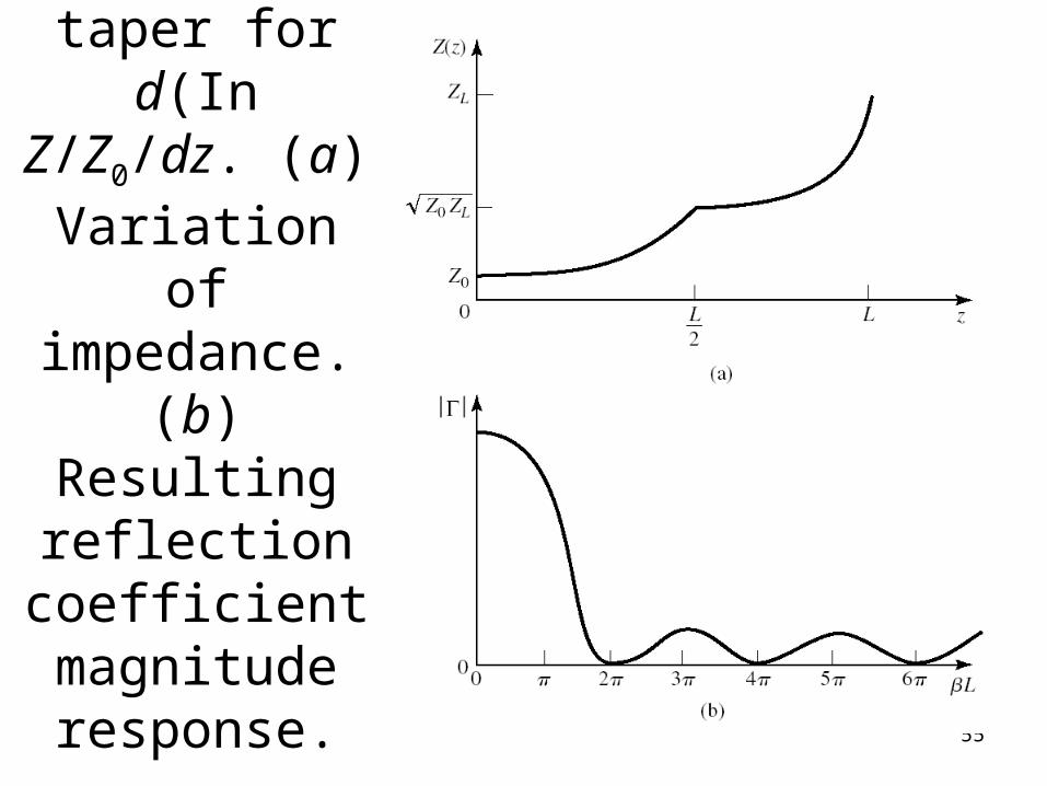
Figure 5.20 (p. 258)
A matching section with a
triangular taper for d(In Z/Z0/dz. (a) Variation of impedance. (b)
Resulting reflection coefficient magnitude response.
56
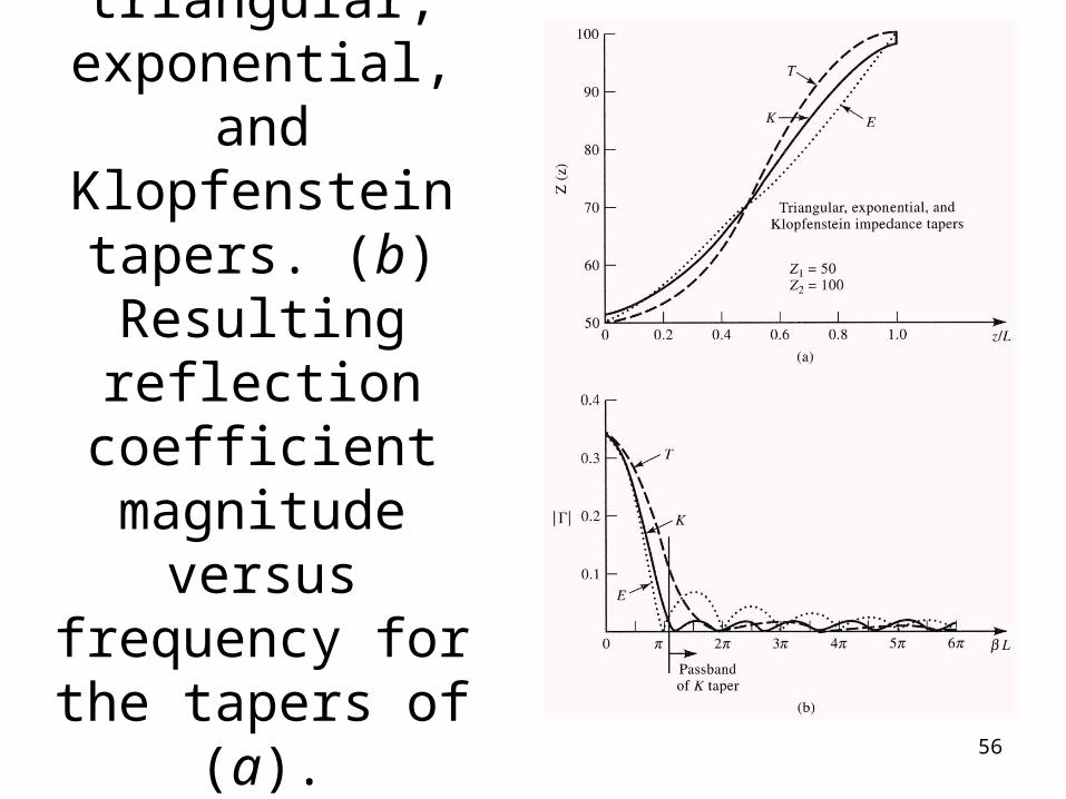
Figure 5.21 (p. 260)
Solution to Example 5.8.
(a) Impedance variations for the
triangular, exponential, and
Klopfenstein tapers. (b) Resulting
reflection coefficient magnitude versus frequency for the
tapers of (a).

57
Figure 5.22 (p. 262)
The Bode-Fano limits for RC and RL loads matched with passive and lossless networks (ω0 is the center frequency of the
matching bandwidth). (a)
Parallel RC. (b) Series RC. (c)
Parallel RL. (d) Series RL.
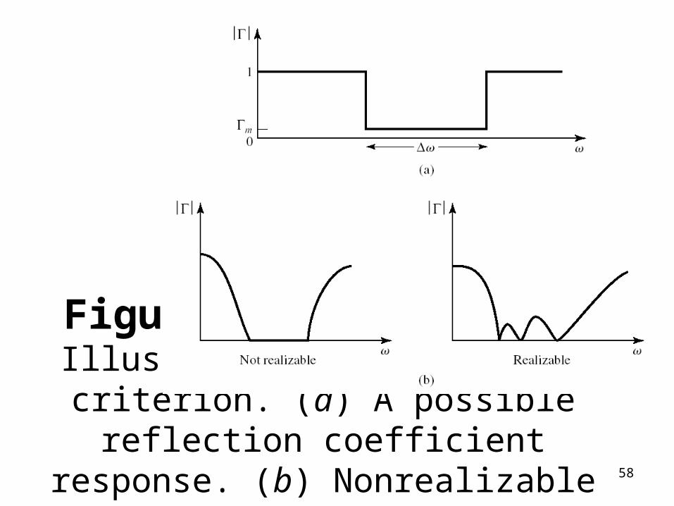
58
Figure 5.23 (p. 263)Illustrating the Bode-Fano criterion. (a) A possible reflection coefficient response. (b)
Nonrealizable and realizable reflection coefficient responses.