1 fault tolerant fpga co-processing toolkit oral defense in partial fulfillment of the requirements...
TRANSCRIPT

1
Fault Tolerant FPGA Co-processing ToolkitFault Tolerant FPGA Co-processing Toolkit
Oral defense in partial fulfillment of the requirements for the degree of Master of Science 2006
Oral defense in partial fulfillment of the requirements for the degree of Master of Science 2006
Douglas Michael DiSabello

2
OverviewOverview
Computation in radiation space environments is slow compared to terrestrial computation
FPGAs can fill and exceed this gap for specific applications
The Fault Tolerant FPGA Co-processing Toolkit facilitates a general capability of FPGA co-processing capability for space based applications
Computation in radiation space environments is slow compared to terrestrial computation
FPGAs can fill and exceed this gap for specific applications
The Fault Tolerant FPGA Co-processing Toolkit facilitates a general capability of FPGA co-processing capability for space based applications

3
OutlineOutline
The Space Computation Performance Gap Ionizing Radiation and FPGA Background Development Board Fault Tolerant Co-Processing Toolkit
Support System Fault Tolerant Support System End User Environment
The Space Computation Performance Gap Ionizing Radiation and FPGA Background Development Board Fault Tolerant Co-Processing Toolkit
Support System Fault Tolerant Support System End User Environment

4
The Space Computation Performance Gap
The Space Computation Performance Gap
Radiation Hardened Microprocessor BAE Systems 133MHz PowerPC Special and proprietary design techniques
Laptop running this presentation 1,500 MHz PowerPC
Radiation Hardened Microprocessor BAE Systems 133MHz PowerPC Special and proprietary design techniques
Laptop running this presentation 1,500 MHz PowerPC

5
Computation Gap ProblemsComputation Gap Problems
Bare minimum of computations performed in space
Large and slow data transfers to limited number of receiving stations
Bare minimum of computations performed in space
Large and slow data transfers to limited number of receiving stations

6
Field Programmable Gate ArraysField Programmable Gate Arrays
200 – 1600 fold speed ups Exploits fine grain parallelism of algorithms
Speed up computations in space beyond what can even be offered by normal terrestrial computers
Fast development cycles In flight reprogramming to adapt to changing
mission requirements
200 – 1600 fold speed ups Exploits fine grain parallelism of algorithms
Speed up computations in space beyond what can even be offered by normal terrestrial computers
Fast development cycles In flight reprogramming to adapt to changing
mission requirements

7
FPGAs DetailsFPGAs Details
SRAM Based Configuration memory stores and implements design Programmed using JTAG or SelectMap interfaces
Configuration Logic Blocks Look Up Tables and supporting logic
Input/Output Blocks Used for all general I/O package pins
Block RAMs General Routing Matrix
SRAM Based Configuration memory stores and implements design Programmed using JTAG or SelectMap interfaces
Configuration Logic Blocks Look Up Tables and supporting logic
Input/Output Blocks Used for all general I/O package pins
Block RAMs General Routing Matrix

8
Ionizing RadiationIonizing Radiation
Low Earth Orbit contains ionizing particles trapped in the Van Allen Belts
Particles cause direct and secondary nuclear reactions in silicon substrate
Decreasing feature sizes and shrinking threshold voltages increase probability of these interactions causing errors in circuits
Low Earth Orbit contains ionizing particles trapped in the Van Allen Belts
Particles cause direct and secondary nuclear reactions in silicon substrate
Decreasing feature sizes and shrinking threshold voltages increase probability of these interactions causing errors in circuits

9
Ionizing Radiation DefinitionsIonizing Radiation Definitions
Single Event Transient Temporary change in logic value
Single Event Upset SET that is latched into a memory
Single Event Functional Interrupt Component stops service
Single Event Transient Temporary change in logic value
Single Event Upset SET that is latched into a memory
Single Event Functional Interrupt Component stops service

10
Ionizing Radiation and FPGAsIonizing Radiation and FPGAs
Architecture SEUs in configuration memory Instantiated design changes Usually results in a SEFI
Data SEUs in Flip Flops, Latches, BRAMS, etc… Incorrect computation results and/or SEFIs
Off Chip Communication Non-dedicated configurable input/outputs package pins SEUs to input/output blocks can disable a package pin

11
Typical FPGA Cross SectionTypical FPGA Cross Section
Configuration Memory accounts for 91% of a typical FPGA cross section 78% - 84.8% Routing Structure 20% Control bits and CLB LUT values
Configuration Memory accounts for 91% of a typical FPGA cross section 78% - 84.8% Routing Structure 20% Control bits and CLB LUT values
Michael Affrey, Paul Graham, Eric Johnson, Michael Wirthlin, Nathan Rollins, and Carl Carmichael, “Single-Event Upsets in SRAM FPGAs” MAPLD, Sep. 2002

12
Fault Mitigation TechniquesFault Mitigation Techniques
Scrubbing fixes architectural upsets Continuously rewrite static portions of
configuration memory Active partial reconfiguration bitstream SEUs corrected at given reconfiguration rate
(shorter than expected upsets rate for given orbit)
Scrubbing fixes architectural upsets Continuously rewrite static portions of
configuration memory Active partial reconfiguration bitstream SEUs corrected at given reconfiguration rate
(shorter than expected upsets rate for given orbit)

13
Fault Mitigation TechniquesFault Mitigation Techniques
Triple Modular Redundancy Allows continuous service when architectural
upsets occur Majority Voters determine final output Inherent data redundancy
Triple Modular Redundancy Allows continuous service when architectural
upsets occur Majority Voters determine final output Inherent data redundancy
14
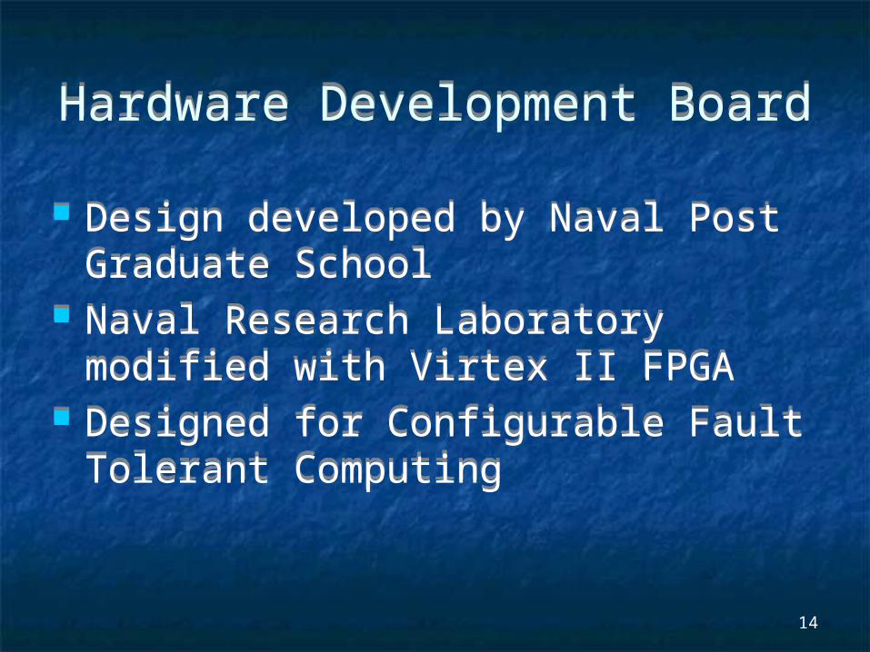
Hardware Development BoardHardware Development Board
Design developed by Naval Post Graduate School
Naval Research Laboratory modified with Virtex II FPGA
Designed for Configurable Fault Tolerant Computing
Design developed by Naval Post Graduate School
Naval Research Laboratory modified with Virtex II FPGA
Designed for Configurable Fault Tolerant Computing

15
Hardware Development BoardHardware Development Board
General I/O
SelectMap
PC104/ISA Bus
JTAG
FLASH
EEPROM
SelectMap
Xilinx VirtexFPGA
Xilinx Virtex IIFPGA
EmbeddedX86 PC
Support FPGA Co-processing FPGA
Only off-chip memory

16
Development Board Radiation TestingDevelopment Board Radiation Testing
NPS and NRL conducted tests at the Crocker Nuclear Lab, U.C. Davis
Protons were emitted from a cyclotron to interact with the FPGAs
Both the Virtex and Virtex II were irradiated
NPS and NRL conducted tests at the Crocker Nuclear Lab, U.C. Davis
Protons were emitted from a cyclotron to interact with the FPGAs
Both the Virtex and Virtex II were irradiated

17
Development Board Radiation TestingDevelopment Board Radiation Testing
Results: 1 upset for every 5 days for the Virtex in orbit Order of magnitude greater for Virtex II in orbit Scrubbing was proven to repair configuration
memory upsets TMR was proven to allow continuous service
between SEU scrubbing intervals
Results: 1 upset for every 5 days for the Virtex in orbit Order of magnitude greater for Virtex II in orbit Scrubbing was proven to repair configuration
memory upsets TMR was proven to allow continuous service
between SEU scrubbing intervals
James C. Coudeyras, “Radiation Testing of The Configurable Fault Tolerant Processor(CFTP) for Space-Based Applications,” Thesis, United States Naval PostGraduate School, 2005

18
The Toolkit ObjectiveThe Toolkit Objective
Build a suite of VHDL designs, C++ software, and tools to give a general FPGA co-processing capability
Modular design for easy integration into new hardware platforms and with new HDL modules
Allow designers to concentrate mainly on the co-processing algorithm and design instead of Fault Tolerance
Build a suite of VHDL designs, C++ software, and tools to give a general FPGA co-processing capability
Modular design for easy integration into new hardware platforms and with new HDL modules
Allow designers to concentrate mainly on the co-processing algorithm and design instead of Fault Tolerance
19
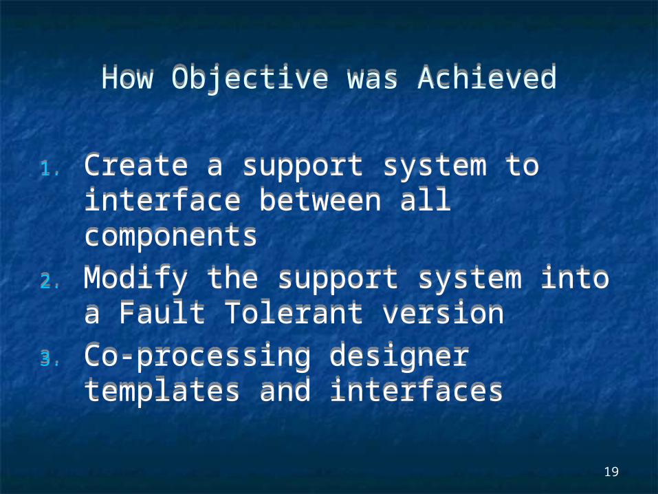
How Objective was AchievedHow Objective was Achieved
1. Create a support system to interface between all components
2. Modify the support system into a Fault Tolerant version
3. Co-processing designer templates and interfaces
1. Create a support system to interface between all components
2. Modify the support system into a Fault Tolerant version
3. Co-processing designer templates and interfaces
20
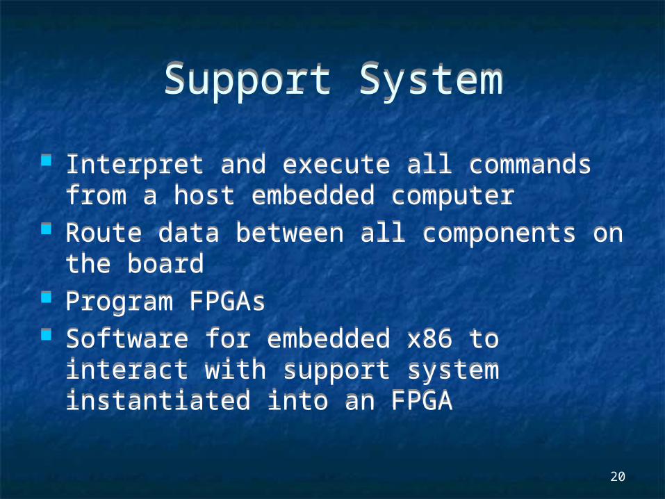
Support SystemSupport System
Interpret and execute all commands from a host embedded computer
Route data between all components on the board
Program FPGAs Software for embedded x86 to interact with
support system instantiated into an FPGA
Interpret and execute all commands from a host embedded computer
Route data between all components on the board
Program FPGAs Software for embedded x86 to interact with
support system instantiated into an FPGA

21
FLASH INTERFACE
VirtexSelectMapInterface
Virtex IISelectMapInterface
FlashArbitrator
PC104/ISA Bus Interfaces
FLASH Control Interface
Inter-FPGACommunication
InterfaceSupport SystemSupport System

22
PC104 / ISA Bus InterfacePC104 / ISA Bus Interface
Responsible for all data transfers on and off the FPGA board
Two addresses from the host PC are used: Data address
8 Bit data words Control address
A write causes the interface to reset and send a reset to any other modules
A read gives the status of the buffer FIFOs Each main support module use a copy of this
interface

23
InputFIFO
OutputFIFO
Bus ControlLogic
Bus Data
EM
PT
Y
RE
AD
EN
AB
LE
FULL
Write Enable
Read Enable
EMPTY
FU
LL
WR
ITE
EN
AB
LE
ADDRESS
Bus Data
BUS DATA
BUS WRITE
BUS READ
AENData Out
Data In
PC104 / ISA Bus InterfacePC104 / ISA Bus Interface

24
Flash ComponentsFlash Components Interface
Translates commands and data into a series of signals to interact with a Flash chip
Control Facilitates interaction between the flash interface and
the Bus Interface Arbitrator
Each module that requires Flash access is given a priority number
A modules must relinquish control before another module can be given access
Interface Translates commands and data into a series of signals
to interact with a Flash chip Control
Facilitates interaction between the flash interface and the Bus Interface
Arbitrator Each module that requires Flash access is given a
priority number A modules must relinquish control before another
module can be given access

25
SelectMap InterfacesSelectMap Interfaces Control configuration data flow to the FPGAs configuration interfaces Configuration Clock is used to allow non-uniform data loading Actual FPGA configuration commands are contained in the
configuration data Two versions: Virtex and Virtex II (and Virtex 4)
Control configuration data flow to the FPGAs configuration interfaces Configuration Clock is used to allow non-uniform data loading Actual FPGA configuration commands are contained in the
configuration data Two versions: Virtex and Virtex II (and Virtex 4)
SelectMapInterface
Flash Address
Flash Interface CMD
Flash Data
Flash Data Valid
Flash Interface Busy
Flash Control Request
Current Flash Owner
SelectMap Data Out <7:0>
Write
Chip Select
Configuration Clock
26
SelectMap Interface CommandsSelectMap Interface Commands
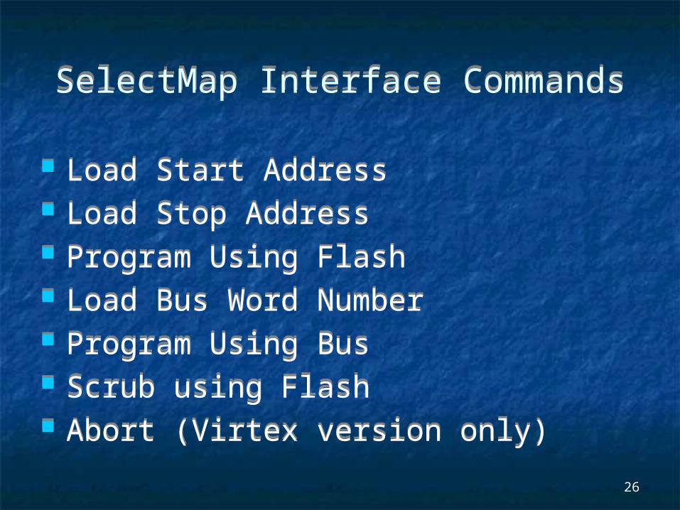
Load Start Address Load Stop Address Program Using Flash Load Bus Word Number Program Using Bus Scrub using Flash Abort (Virtex version only)
Load Start Address Load Stop Address Program Using Flash Load Bus Word Number Program Using Bus Scrub using Flash Abort (Virtex version only)

27
Inter-FPGA Communication InterfaceInter-FPGA Communication Interface
Modified ISA Bus interface for delays between physical FPGA chips
Co-processing FPGA has direct access to BUS and own memory space
Designed specifically to use resources of support FPGA
Modified ISA Bus interface for delays between physical FPGA chips
Co-processing FPGA has direct access to BUS and own memory space
Designed specifically to use resources of support FPGA

28
x86 Host PC Programsx86 Host PC Programs
Flash program Flash verify SelectMap Configuration Scrub On and Scrub Off Co-processing echo check program
Flash program Flash verify SelectMap Configuration Scrub On and Scrub Off Co-processing echo check program

29
Fault Tolerant Support SystemFault Tolerant Support System
Add fault tolerance to original support system
Specialized fault mitigation techniques FPGA configuration, scrubbing, and
BitStream manipulation Support System End User Environment
Add fault tolerance to original support system
Specialized fault mitigation techniques FPGA configuration, scrubbing, and
BitStream manipulation Support System End User Environment
30
Support System Main Fault Tolerance Methods
Support System Main Fault Tolerance Methods
Triple Modular Redundancy All modules are made in triplicate Majority voter determines correct output Between HDL modules three voters are used
to keep redundancy of signal paths Place and Route to keep redundant modules
separate
Triple Modular Redundancy All modules are made in triplicate Majority voter determines correct output Between HDL modules three voters are used
to keep redundancy of signal paths Place and Route to keep redundant modules
separate
31
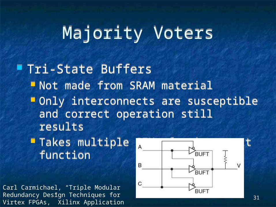
Majority VotersMajority Voters
Tri-State Buffers Not made from SRAM material Only interconnects are susceptible and
correct operation still results Takes multiple SEUs for incorrect function
Tri-State Buffers Not made from SRAM material Only interconnects are susceptible and
correct operation still results Takes multiple SEUs for incorrect function
Carl Carmichael, “Triple Modular Redundancy Design Techniques for Virtex FPGAs,” Xilinx Application Note 197, 2001

32
FSMs and TMRFSMs and TMR
Method keeps FSM synchronized if SEU occurs in state register
Outputs are also majority voted
Method keeps FSM synchronized if SEU occurs in state register
Outputs are also majority voted
Current State Register
Current State Register
Current State Register
Next StateLogic
Next StateLogic
Next StateLogic
INPUTS
V
V
V
33
Block RAM Fault MitigationBlock RAM Fault Mitigation
TMR Necessary for routing structure Inherent data redundancy Method is fine for short term data storage SEUs are not corrected during long term data
storage in individual BRAM
TMR Necessary for routing structure Inherent data redundancy Method is fine for short term data storage SEUs are not corrected during long term data
storage in individual BRAM

34
BRAM TMR w/ RefreshBRAM TMR w/ Refresh
All BRAMs are dual ported Second ports are used to constantly read
data values from three copies, vote, and rewrite the values
Data write collision avoidance Not needed for support system, but useful
for co-processing applications
All BRAMs are dual ported Second ports are used to constantly read
data values from three copies, vote, and rewrite the values
Data write collision avoidance Not needed for support system, but useful
for co-processing applications
Carl Carmichael, “Triple Modular Redundancy Design Techniques for Virtex FPGAs,” Xilinx Application Note 197, 2001

35
Specialized TechniquesSpecialized Techniques
Off FPGA transfers TMR of package pins to a single trace TMR of package pins not available on
development board
Off FPGA transfers TMR of package pins to a single trace TMR of package pins not available on
development board
Carl Carmichael, “Triple Modular Redundancy Design Techniques for Virtex FPGAs,” Xilinx Application Note 197, 2001
36
Specialized TechniquesSpecialized Techniques
Inter-FPGA transfers Not enough pins available to triplicate all
signals 8 data bit and 4 redundant bit Hamming code
used for data Double Error Detection and Single Error
Correction Triplication of all other signals
Inter-FPGA transfers Not enough pins available to triplicate all
signals 8 data bit and 4 redundant bit Hamming code
used for data Double Error Detection and Single Error
Correction Triplication of all other signals

37
Specialized TechniquesSpecialized Techniques
PC104 / ISA Bus transfers Updated fault tolerant module allows for
extended data transfer sizes All data sent is encoded in (8,4) hamming
code No redundancy available for other signals
PC104 / ISA Bus transfers Updated fault tolerant module allows for
extended data transfer sizes All data sent is encoded in (8,4) hamming
code No redundancy available for other signals

38
Flash Memory Data ReadsFlash Memory Data Reads
CRC values embedded every 512 16-bit flash words by Flash program
Fault tolerant Flash interface uses BRAM buffer cache to hold every 512 blocks of data when data is requested
If CRC value is incorrect data cache is flushed and the data is read again
CRC values embedded every 512 16-bit flash words by Flash program
Fault tolerant Flash interface uses BRAM buffer cache to hold every 512 blocks of data when data is requested
If CRC value is incorrect data cache is flushed and the data is read again

39
Configuration and ScrubbingConfiguration and Scrubbing
Three modes of configuration determined by the bit file created using Xilinx Bitgen tool Initial Configuration
Contains startup commands Reconfiguration
Contains shutdown and startup commands Doesn’t require a powercycle, but FPGA is taken out of service
Active Partial Reconfiguration Used for scrubbing Rewrites static portions of bitstream Removes initial BRAM contents Any portion of design could be masked out

40
Support System End User EnvironmentSupport System End User Environment
Flash program and verify host programs Store initial co-processing, co-processing scrubbing,
and support scrubbing bitstreams at designated flash addresses
Scrub On and Off Selectmap interfaces begin scrubbing at given
periods using flash data configuration can also still be done across the bus
C++ examples programs and headers files for data transfers to the co-processing FPGA

41
Toolkit User EnvironmentToolkit User Environment
Fault Tolerant Support System Controls all data flow Modular design for quick integration to different
physical systems with varying number of FPGAs C++ programs and header files
Co-Processing Tools Templates for HDL co-processing components HDL “hooks” for data transfers C++ programs and header files

42
Future Toolkit AdditionsFuture Toolkit Additions
Different bus modules for interaction with radiation hardened microprocessors
Co-processing library Use support system on single and multiple
FPGA boards
Different bus modules for interaction with radiation hardened microprocessors
Co-processing library Use support system on single and multiple
FPGA boards