1. general description - nxp semiconductors · 1. general description ... implements snk role...
TRANSCRIPT
1. General description
PTN5110 is a single-port TCPC compliant USB Power Delivery (PD) PHY IC that implements Type-C Configuration Channel (CC) interface and USB PD Physical layer functions to a Type-C Port Manager (TCPM) that handles PD Policy management. It is designed to comply with USB PD [1], Type-C [2] and TCPC [3] specifications. This IC is targeted primarily for use in system platforms (e.g. Notebook PCs, Desktop PCs, Chromebooks, Tablets, Convertibles, etc.). Other use cases may be feasible depending on the application architecture, e.g. docks, monitors, accessories, cable adapters, smartphones etc.
It can support various Type-C roles: Sink, Source, Sink with accessory support or DRP. It implements Type-C CC analog portion (i.e Rd/Rp/Ra detection, Rd/Rp indication) and PD Tx/Rx PHY and protocol state machines as per [3]. PTN5110 supports TCPM in system realization of the following PD roles:
1. Provider (P)
2. Provider/Consumer (P/C)
3. Consumer (C)
4. Consumer/Provider (C/P)
PTN5110 integrates VCONN load switch with programmable current limit, reverse leakage current blocking and Over Temperature Protection (OTP). It implements two enable control outputs for controlling load switches/FETs on VBUS source and/or sink power paths. It also implements VBUS voltage monitoring/measurement, VBUS Force discharge and Bleed discharge features as defined in [3]. PTN5110 implements I2C-bus interface registers, finite state machines and control flow, etc. as defined in [3]. Please refer to [3] for description of I2C registers, control descriptions, flow diagrams, etc.
PTN5110 provides the majority of relevant IO capability for the host processor/TCPM to easily control and manage the Type-C/PD interface via the TCPC interface:
• VBUS Power path control of source and sink power rails (EN_SRC, EN_SNK1)
• Up to four different slave addresses can be selected based on SLV_ADDR
• ILIM_5V_VBUS that allows TCPM to set two different current limits on VBUS 5 V Load switch.
• FRS_EN that allows for arming 5 V SRC load switch for Fast Role Swap (FRS) support
• DBG_ACC that can be used by host TCPM indicate Type-C debug accessory detection
PTN5110 offers tremendous flexibility to platform integrators by supporting a wide range of power supply input voltages.
PTN5110USB PD TCPC PHY ICRev. 1.5 — 25 January 2018 Product data sheet

NXP Semiconductors PTN5110USB PD TCPC PHY IC
PTN5110 is available in HX2QFN16, 2.6 mm x 2.6 mm x 0.35 mm, 0.4 mm pitch.
Remark:
1. PTN5110 provides independently controllable pull-up resistor (Rp) implementations on CC1 and CC2 pins.
2. PTN5110 can detect/monitor voltage levels independently on each CC pin.
2. Features and benefits
2.1 USB PD and Type-C features
Designed to comply with USB PD[1], USB Type-C [2] and TCPC [3] specifications
Supports Type-C functionality as per [2][3]
Provides CC analog functions: Rp and Rd/GND dynamic indication and Rp/Rd/Ra dynamic detection, debouncing of CC pins, dynamic selection of different Rp/Rd values for CC1 and CC2 independently
Implements SNK role pull-down (Rd) behavior to handle dead battery/no power condition
Support for Type-C Debug Accessory detection and orientation detection (refer to Appendix of [2]) for Source and Sink Target Systems (TS). Indication of the result via dedicated pin (DBG_ACC) and status registers.
Plug orientation detection and indication via status register(s)
Supports integrated VCONN switch(es) delivering power to accessory
Cooperatively work under TCPM control for Type-C Connection/Disconnection Detection, Power Delivery negotiation and contract(s), Alternate mode support, VDM exchanges and any custom functions
Implements TCPC functionality as per [3]
SOP* Configurable: Register programmable to generate and receive SOP, SOP’, SOP’-debug, SOP”, SOP”-debug”
Supports Extended messaging Unchunked and Chunked based packet transport
VBUS Bleed and Force discharge schemes are implemented as per [3]
Implements VCONN discharge on Hard Reset (TCPM Controlled)
Implements Fast Role Swap request detection (in 'initial sink' role) and indication (in 'initial source' role)
Supports VBUS source/sink power path control
Supports Seamless VBUS source voltage transitions among PD voltage rails (e.g. using Load switches - 5 V VBUS source switch - NX5P3290, High Voltage VBUS source switch):
- For positive voltage transitions, PTN5110 implements make-before-break feature (turn on higher voltage rail first and turn off lower voltage rail after a programmable time duration determined by summation of turn-on time and enable time of higher voltage rail load switch).
- For negative voltage transitions, PTN5110 disables higher voltage rail load switch initially, performs force discharge and monitors VBUS voltage until stop threshold is reached and enables lower voltage rail load switch when VBUS voltage reaches equal to (or slightly less than) the programmed rail voltage in the TCPC I2C VBUS voltage Alarm register.
PTN5110 All information provided in this document is subject to legal disclaimers. © NXP Semiconductors N.V. 2018. All rights reserved.
Product data sheet Rev. 1.5 — 25 January 2018 2 of 60
NXP Semiconductors PTN5110USB PD TCPC PHY IC
For a multi-port system implementation, PTN5110 allows for
- TCPM initiated VBUS Sink path transitions from one Type-C port to another Type-C port using NXP High voltage sink switch (NX20P5090)
- Single VBUS Sink power path enabling under dead battery (when multiple Type-C ports can provide VBUS 5 V power)
2.2 System protection features
Back current protection on all pins when PTN5110 is unpowered
CC pins are 6 V tolerant
2.3 General
Provides two Power path enable controls: EN_SRC, EN_SNK1
TCPM Host interface control and status update handled via I2C-bus interface. Supports I2C slave interface standard mode (100 kHz), Fast mode (400 kHz) and Fast mode plus (1 MHz)
Up to four I2C device slave address options selectable via SLV_ADDR pin. This allows for multi-port implementation with PTN5110
Supports register access: device configuration, control and status/interrupt interfacing through Slave I2C-bus conforming to [3]
Power supply: VDD range (2.7 V to 5.5 V) and VBUS (4 V to 25 V)
Tolerant up to 28 V on VBUS (and operational up to maximum of 25 V on VBUS)
Ambient operating temperature range 40 to 85 C ESD 8 kV HBM, 1 kV CDM
Package: HX2QFN16, 2.6 mm x 2.6 mm x 0.35 mm, 0.4 mm pitch
PTN5110 All information provided in this document is subject to legal disclaimers. © NXP Semiconductors N.V. 2018. All rights reserved.
Product data sheet Rev. 1.5 — 25 January 2018 3 of 60

NXP Semiconductors PTN5110USB PD TCPC PHY IC
3. Applications
PC platforms: Notebook PCs, Desktop PCs, Ultrabooks, Chromebooks
Tablets, 2:1 Convertibles, Smartphones and Portable devices
PC accessories/peripherals: Docking, Mobile Monitors, Multi-Function Monitors, Portable/External hard drives, Cable adaptors, Dongles and accessories, etc.
PTN5110 All information provided in this document is subject to legal disclaimers. © NXP Semiconductors N.V. 2018. All rights reserved.
Product data sheet Rev. 1.5 — 25 January 2018 4 of 60
NXP Semiconductors PTN5110USB PD TCPC PHY IC
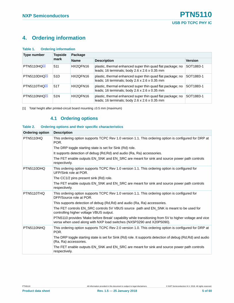
4. Ordering information
[1] Total height after printed-circuit board mounting 0.5 mm (maximum)
4.1 Ordering options
Table 1. Ordering information
Type number Topside mark
Package
Name Description Version
PTN5110HQ[1] 511 HX2QFN16 plastic, thermal enhanced super thin quad flat package; no leads; 16 terminals; body 2.6 x 2.6 x 0.35 mm
SOT1883-1
PTN5110DHQ[1] 51D HX2QFN16 plastic, thermal enhanced super thin quad flat package; no leads; 16 terminals; body 2.6 x 2.6 x 0.35 mm
SOT1883-1
PTN5110THQ[1] 51T HX2QFN16 plastic, thermal enhanced super thin quad flat package; no leads; 16 terminals; body 2.6 x 2.6 x 0.35 mm
SOT1883-1
PTN5110NHQ[1] 51N HX2QFN16 plastic, thermal enhanced super thin quad flat package; no leads; 16 terminals; body 2.6 x 2.6 x 0.35 mm
SOT1883-1
Table 2. Ordering options and their specific characteristics
Ordering option Description
PTN5110HQ This ordering option supports TCPC Rev 1.0 version 1.1. This ordering option is configured for DRP at POR.
The DRP toggle starting state is set for Sink (Rd) role.
It supports detection of debug (Rd,Rd) and audio (Ra, Ra) accessories.
The FET enable outputs EN_SNK and EN_SRC are meant for sink and source power path controls respectively.
PTN5110DHQ This ordering option supports TCPC Rev 1.0 version 1.1. This ordering option is configured for UFP/Sink role at POR.
The CC1/2 pins present sink (Rd) role.
The FET enable outputs EN_SNK and EN_SRC are meant for sink and source power path controls respectively.
PTN5110THQ This ordering option supports TCPC Rev 1.0 version 1.1. This ordering option is configured for DFP/Source role at POR.
This supports detection of debug (Rd,Rd) and audio (Ra, Ra) accessories.
The FET controls EN_SRC controls 5V VBUS source path and EN_SNK is meant to be used for controlling higher voltage VBUS output.
PTN5110 provides 'Make before Break' capability while transitioning from 5V to higher voltage and vice versa when used along with NXP load switches (NX5P3290 and X20P5090).
PTN5110NHQ This ordering option supports TCPC Rev 2.0 version 1.0. This ordering option is configured for DRP at POR.
The DRP toggle starting state is set for Sink (Rd) role. It supports detection of debug (Rd,Rd) and audio (Ra, Ra) accessories.
The FET enable outputs EN_SNK and EN_SRC are meant for sink and source power path controls respectively.
PTN5110 All information provided in this document is subject to legal disclaimers. © NXP Semiconductors N.V. 2018. All rights reserved.
Product data sheet Rev. 1.5 — 25 January 2018 5 of 60
NXP Semiconductors PTN5110USB PD TCPC PHY IC
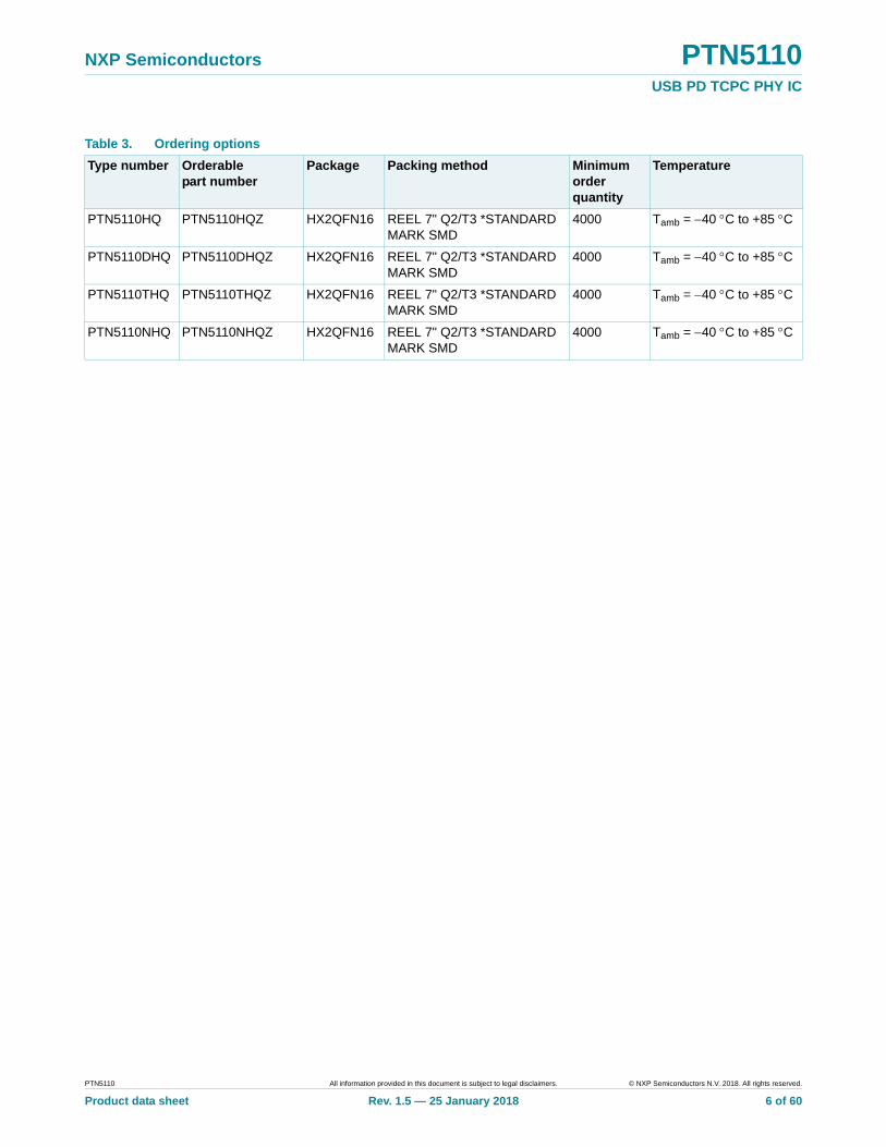
Table 3. Ordering options
Type number Orderable part number
Package Packing method Minimum order quantity
Temperature
PTN5110HQ PTN5110HQZ HX2QFN16 REEL 7" Q2/T3 *STANDARD MARK SMD
4000 Tamb = 40 C to +85 C
PTN5110DHQ PTN5110DHQZ HX2QFN16 REEL 7" Q2/T3 *STANDARD MARK SMD
4000 Tamb = 40 C to +85 C
PTN5110THQ PTN5110THQZ HX2QFN16 REEL 7" Q2/T3 *STANDARD MARK SMD
4000 Tamb = 40 C to +85 C
PTN5110NHQ PTN5110NHQZ HX2QFN16 REEL 7" Q2/T3 *STANDARD MARK SMD
4000 Tamb = 40 C to +85 C
PTN5110 All information provided in this document is subject to legal disclaimers. © NXP Semiconductors N.V. 2018. All rights reserved.
Product data sheet Rev. 1.5 — 25 January 2018 6 of 60
NXP Semiconductors PTN5110USB PD TCPC PHY IC
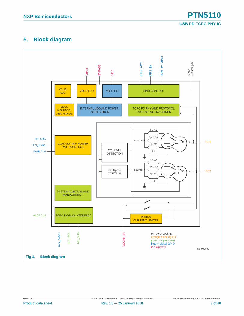
5. Block diagram
Fig 1. Block diagram
aaa-022981
VBUSADC VBUS LDO
VBUSMONITOR/
DISCHARGE
INTERNAL LDO AND POWERDISTRIBUTION
LOAD-SWITCH POWERPATH CONTROL
EN_SRC
EN_SNK1
FAULT_N
ALERT_N
SLV
_AD
DR
I2C
_SC
L
I2C
_SD
A
VC
ON
N_I
N
CC LEVELDETECTION
CC Rp/RdCONTROL
VCONNCURRENT LIMITER
CC1
GN
D(c
ente
r pad
)
CC2
Pin color coding:orange = analog I/Ogreen = open-drainblue = digital GPIOred = power
SYSTEM CONTROL ANDMANAGEMENT
TCPC I2C-BUS INTERFACE
GPIO CONTROL
source
Rp, 3A
Rp, 1.5A
Rp, std
Rd
Rp, 3A
Rp, 1.5A
Rp, std
Rd
TCPC PD PHY AND PROTOCOLLAYER STATE MACHINES
VDD LDO
source
FRS
_EN
ILIM
_5V
_VB
US
DB
G_A
CC
VB
US
BY
PA
SS
VD
D
PTN5110 All information provided in this document is subject to legal disclaimers. © NXP Semiconductors N.V. 2018. All rights reserved.
Product data sheet Rev. 1.5 — 25 January 2018 7 of 60

NXP Semiconductors PTN5110USB PD TCPC PHY IC
6. Pinning information
6.1 Pinning
6.2 Pin description
(1) This is GND center pad on the bottom side of the package
Fig 2. Pin configuration (transparent top view)
aaa-022982
1FRS_EN
PTN5110(1)2EN_SNK1
3VDD
4BYPASS
5SLV_ADDR
13 CC1
12 VCONN_IN
11 FAULT_N
10 ALERT_N
9 DBG_ACC
16E
N_S
RC
15V
BU
S
14C
C2
6IL
IM_5
V_V
BU
S
7I2
C_S
DA
8I2
C_S
CL
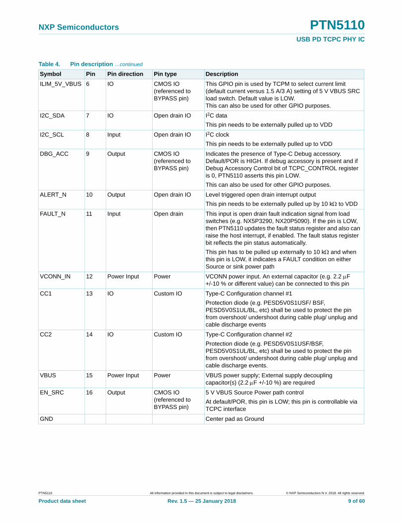
Table 4. Pin description
Symbol Pin Pin direction Pin type Description
FRS_EN 1 Output CMOS IO (referenced to BYPASS pin)
This pin is used by TCPM for FRS enable control of a 5 V SRC Load switch (e.g. FO pin of NX5P3290).
Default value is LOW.
This can also be used for other GPIO purposes.
EN_SNK1 2 Output CMOS IO (referenced to BYPASS pin)
VBUS Sink Power path control output.
At default/POR, this pin is LOW.
This pin is controllable via TCPC interface. This can also be used for VBUS source power path control in PD source only applications
VDD 3 Power Input Power Core domain power supply; (2.7 V to 5.5 V)
External supply decoupling capacitor(s) (2.2 F +/-10 %) are required
BYPASS 4 Internal Internal power rail Internal node
An external capacitor (e.g. 2.2 F +/-20 %) is required to be connected to this pin
SLV_ADDR 5 IO Quaternary Input I2C slave address selection pin. This pin is wired to BYPASS pin (in the PCB) for two of the four SLV_ADDR options. This pin is sampled at POR only.
PTN5110 All information provided in this document is subject to legal disclaimers. © NXP Semiconductors N.V. 2018. All rights reserved.
Product data sheet Rev. 1.5 — 25 January 2018 8 of 60
NXP Semiconductors PTN5110USB PD TCPC PHY IC
ILIM_5V_VBUS 6 IO CMOS IO (referenced to BYPASS pin)
This GPIO pin is used by TCPM to select current limit (default current versus 1.5 A/3 A) setting of 5 V VBUS SRC load switch. Default value is LOW.This can also be used for other GPIO purposes.
I2C_SDA 7 IO Open drain IO I2C data
This pin needs to be externally pulled up to VDD
I2C_SCL 8 Input Open drain IO I2C clock
This pin needs to be externally pulled up to VDD
DBG_ACC 9 Output CMOS IO (referenced to BYPASS pin)
Indicates the presence of Type-C Debug accessory. Default/POR is HIGH. If debug accessory is present and if Debug Accessory Control bit of TCPC_CONTROL register is 0, PTN5110 asserts this pin LOW.
This can also be used for other GPIO purposes.
ALERT_N 10 Output Open drain IO Level triggered open drain interrupt output
This pin needs to be externally pulled up by 10 k to VDD
FAULT_N 11 Input Open drain This input is open drain fault indication signal from load switches (e.g. NX5P3290, NX20P5090). If the pin is LOW, then PTN5110 updates the fault status register and also can raise the host interrupt, if enabled. The fault status register bit reflects the pin status automatically.
This pin has to be pulled up externally to 10 k and when this pin is LOW, it indicates a FAULT condition on either Source or sink power path
VCONN_IN 12 Power Input Power VCONN power input. An external capacitor (e.g. 2.2 F +/-10 % or different value) can be connected to this pin
CC1 13 IO Custom IO Type-C Configuration channel #1
Protection diode (e.g. PESD5V0S1USF/ BSF, PESD5V0S1UL/BL, etc) shall be used to protect the pin from overshoot/ undershoot during cable plug/ unplug and cable discharge events
CC2 14 IO Custom IO Type-C Configuration channel #2
Protection diode (e.g. PESD5V0S1USF/BSF, PESD5V0S1UL/BL, etc) shall be used to protect the pin from overshoot/ undershoot during cable plug/ unplug and cable discharge events.
VBUS 15 Power Input Power VBUS power supply; External supply decoupling capacitor(s) (2.2 F +/-10 %) are required
EN_SRC 16 Output CMOS IO (referenced to BYPASS pin)
5 V VBUS Source Power path control
At default/POR, this pin is LOW; this pin is controllable via TCPC interface
GND Center pad as Ground
Table 4. Pin description …continued
Symbol Pin Pin direction Pin type Description
PTN5110 All information provided in this document is subject to legal disclaimers. © NXP Semiconductors N.V. 2018. All rights reserved.
Product data sheet Rev. 1.5 — 25 January 2018 9 of 60
NXP Semiconductors PTN5110USB PD TCPC PHY IC
7. Functional description
PTN5110 is a TCPC compliant USB Type-C PD PHY IC that can be used to realize single or multi-port USB Type-C PD and/or Alternate mode implementations. It is designed to comply with USB PD [1], Type-C [2] and TCPC [3] specifications.
PTN5110 can be partitioned into the following major functional blocks along with their respective interfaces:
• Type-C Configuration Channel function
• USB Power Delivery function
• VCONN switch and control
• VBUS Power path Control
• TCPC I2C-bus interface and Control
• Power management
• Power supply
The following subsections describe the PTN5110 with its major functional blocks.
7.1 Type-C Configuration Channel functional block
Type-C Configuration Channel (CC) function operates as a front end to cable/plug interface. This block implements Orientation detection (TCPM detects orientation and informs TCPC of the result), Cable/Plug insertion (only initial indication, TCPM verifies connection and tells TCPC when the connection is valid) and removal detection under different roles (SRC, DRP, SNK including accessory support) as per [2][3].
In particular, PTN5110 supports Type-C functionality
• Applying 'Rp (for CC1)', 'Rp (for CC2)', or 'Rd' depending on the configured role
• Detecting cable/plug connect and disconnect events
• Indicating Type-C current limit level in a system under Source role
• Detecting the current level supported by remote end under Sink role
• Supports TCPM in identifying plug orientation and indicating through TCPCi register interface
• Implements VBUS thresholds, monitoring and measurement
• Discharging VBUS and VCONN based on Type-C status/PD Policy (managed by TCPM)
• Supports TCPM in identifying Type-C Debug accessory detection and indicating through TCPCi register interface and DBG_ACC pin. TCPM implements Type-C Debug scheme
• Supports TCPM in Audio accessory detection and indication via status register
• Updating event, interrupt and status registers using ALERT_N pin
• Try.SRC/ Try.SNK feature can be enabled
PTN5110 All information provided in this document is subject to legal disclaimers. © NXP Semiconductors N.V. 2018. All rights reserved.
Product data sheet Rev. 1.5 — 25 January 2018 10 of 60
NXP Semiconductors PTN5110USB PD TCPC PHY IC
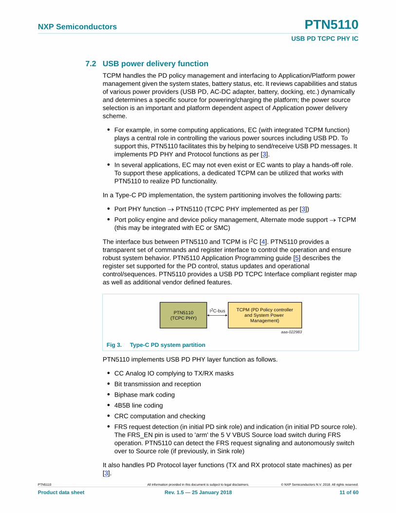
7.2 USB power delivery function
TCPM handles the PD policy management and interfacing to Application/Platform power management given the system states, battery status, etc. It reviews capabilities and status of various power providers (USB PD, AC-DC adapter, battery, docking, etc.) dynamically and determines a specific source for powering/charging the platform; the power source selection is an important and platform dependent aspect of Application power delivery scheme.
• For example, in some computing applications, EC (with integrated TCPM function) plays a central role in controlling the various power sources including USB PD. To support this, PTN5110 facilitates this by helping to send/receive USB PD messages. It implements PD PHY and Protocol functions as per [3].
• In several applications, EC may not even exist or EC wants to play a hands-off role. To support these applications, a dedicated TCPM can be utilized that works with PTN5110 to realize PD functionality.
In a Type-C PD implementation, the system partitioning involves the following parts:
• Port PHY function PTN5110 (TCPC PHY implemented as per [3])
• Port policy engine and device policy management, Alternate mode support TCPM (this may be integrated with EC or SMC)
The interface bus between PTN5110 and TCPM is I2C [4]. PTN5110 provides a transparent set of commands and register interface to control the operation and ensure robust system behavior. PTN5110 Application Programming guide [5] describes the register set supported for the PD control, status updates and operational control/sequences. PTN5110 provides a USB PD TCPC Interface compliant register map as well as additional vendor defined features.
PTN5110 implements USB PD PHY layer function as follows.
• CC Analog IO complying to TX/RX masks
• Bit transmission and reception
• Biphase mark coding
• 4B5B line coding
• CRC computation and checking
• FRS request detection (in initial PD sink role) and indication (in initial PD source role). The FRS_EN pin is used to 'arm' the 5 V VBUS Source load switch during FRS operation. PTN5110 can detect the FRS request signaling and autonomously switch over to Source role (if previously, in Sink role)
It also handles PD Protocol layer functions (TX and RX protocol state machines) as per [3].
Fig 3. Type-C PD system partition
aaa-022983
PTN5110(TCPC PHY)
TCPM (PD Policy controllerand System Power
Management)
I2C-bus
PTN5110 All information provided in this document is subject to legal disclaimers. © NXP Semiconductors N.V. 2018. All rights reserved.
Product data sheet Rev. 1.5 — 25 January 2018 11 of 60
NXP Semiconductors PTN5110USB PD TCPC PHY IC
To minimize chances of collision, PTN5110 checks the CC line before start of transmission. Once the data is transmitted or received, the I2C-bus interface status is updated and TCPM is interrupted. It also provides support for a bus management scheme as defined in [1].
BIST mode (Tx, Rx) is also supported.
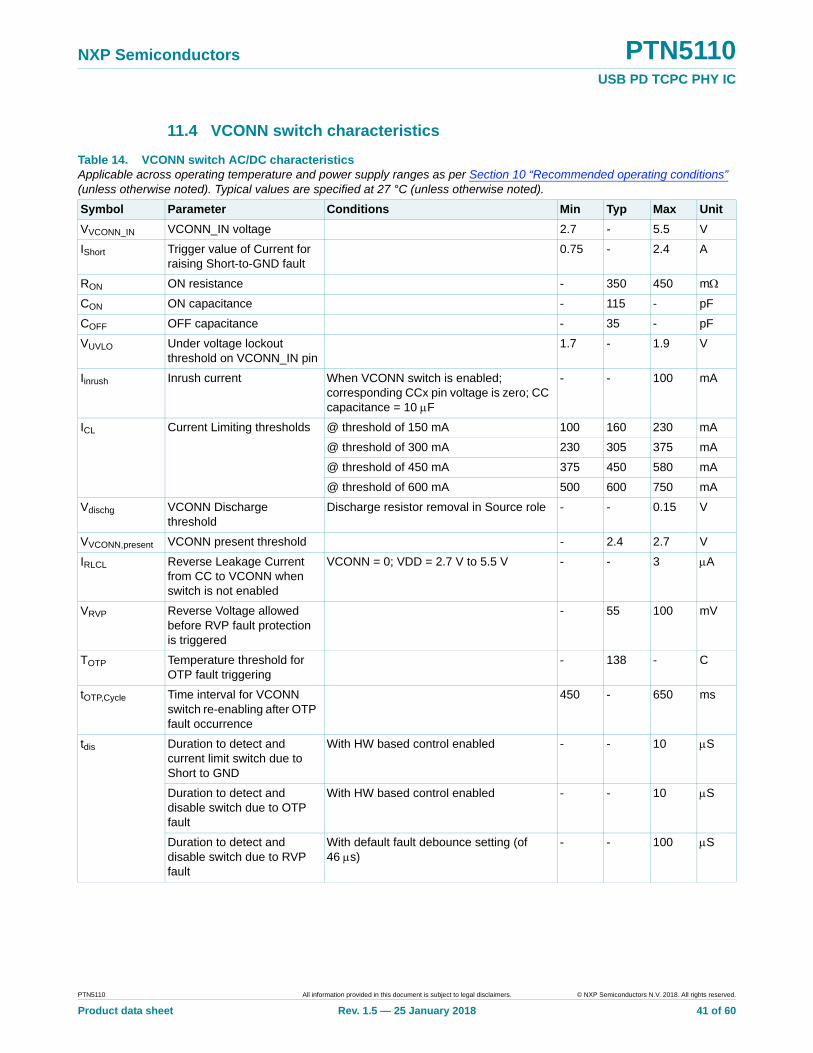
7.3 VCONN switch and control
PTN5110 implements a very low RON switch that can deliver VCONN current; depending on the pin over which CC communication is established, VCONN_IN power is delivered into the other CC pin. With its patented architecture, the switch implements Soft Start behavior to avoid heavy inrush current flow when it is enabled. The VCONN switch and protection circuitry can be activated only when VCONN_IN is above VCONN present threshold. When in disabled condition, PTN5110 presents Hi-Z condition on the corresponding CCx pin.
The switch implements four important features relevant to application robustness
• Reverse Voltage Protection (RVP)
• Over Current Limiting (OCL)
• Over Temperature Protection (OTP)
• Short to GND protection
The fault conditions are mapped to VCONN fault status and interrupt bits in TCPC registers. There is an extended set of VCONN registers for configuring the deglitch duration, reattempt count re-assert delay, interrupt mask, fault status, etc. The TCPM can program these registers during TCPC initialization to achieve desired behavior. [5] provides more details on the registers and bit definitions.
7.3.1 Reverse Voltage Protection (RVP)
PTN5110 implements RVP that monitors for a certain voltage difference (over the deglitch duration) to disable the switch path and protect the system from reverse current flow. After the ‘reassert delay’ is elapsed, PTN5110 enables the switch again. If the condition persists for 'reattempt count', then RVP fault status is asserted and if the interrupt is not masked, it would raise ALERT_N for the host TCPM to take corrective measures. The ‘reassert delay’ and ‘reattempt count’ are defined in [5].
TCPM can program the deglitch duration, reassert delay, reattempt count via extended registers [5] at TCPCi level. The reverse voltage protection circuit can only be triggered when it is enabled.
PTN5110 also provides reverse leakage current blocking when the switch is not enabled. Irrespective of VCONN_IN pin voltage, the reverse leakage current (IRLCL) on CC1/2 pin is LOW.
7.3.2 Over Current Limiting (OCL)
PTN5110 supports four OCL threshold programmable levels. The Over Current Limiting (OCL) circuitry keeps monitoring for current flow above the pre configured level and whenever the threshold is exceeded, the switch goes into current limiting mode. It is possible for the switch to go into Over Temperature condition due to heating and go into OTP temperature cycling.
PTN5110 All information provided in this document is subject to legal disclaimers. © NXP Semiconductors N.V. 2018. All rights reserved.
Product data sheet Rev. 1.5 — 25 January 2018 12 of 60
NXP Semiconductors PTN5110USB PD TCPC PHY IC
7.3.3 Over Temperature Protection (OTP)
If the switch has been enabled and if the device temperature exceeds a preset threshold, the device goes into Over Temperature condition. The OTP circuit disables the switch and triggers the fault status and raise interrupt (if enabled). Once the temperature reduces down to 85°C and after OTP reassert delay duration [5], the switch is enabled automatically. The TCPM can trigger disabling of the switch, if required.
7.3.4 Short to GND protection
PTN5110 can protect the system from hard short to GND. Whenever the current delivered goes beyond the highest threshold and up to Ishort, PTN5110 turns off the switch within a few microseconds, enables the switch limiting the current flow up to the pre-programmed OCL limit. PTN5110 records the fault status and generate interrupt (if enabled). The TCPM can trigger disabling of the switch, if required.
7.4 VBUS power path control
Based on PD negotiation and contract, TCPM enables/disables specific power path (source or sink load switches). PTN5110 provides two power path control IO pins. They are:
• EN_SRC: This is meant for 5 V Source control
– ILIM_5V_VBUS is provided to control current limiting at default current (0.9 A) versus 1.5/3 A
• EN_SNK1: This is meant for sinking current from VBUS (or, it can be configured to source a second power rail in a two-rail source system)
Remark: Platform integrators may use MOSFETs (with additional control circuitry) instead of Load switches while using PTN5110 in their applications.
With the support of NXP (RCP capable) Type-C Load switches, PTN5110 supports
• FRS operation
• Positive and Negative voltage transitions (while in SRC mode with two power rails)
• In a multi-port platform with buck boost configuration and dead battery condition, EN_SNK1 pin activates NX20P5090 allowing current flow into the system. It is possible that this could potentially lead to multiple ports allowing sink current at 5 V into the system. Once the system initializes, the TCPM can selectively charge from a port only.
Table 5. Power path combination illustration
Configuration (not limited to) Load switch* Combination
(e.g. NX5P3290, NX20P5090, Source side Load switch)
5 V Source, 5 V to 20 V Sink Source Load switch w/OCL = NX5P3290 (EN_SRC)
Sink Load switch w/RCP = NX20P5090 (EN_SNK1)
5 V Source, 5 V to 20 V Sink Source Load switch w/OCL = NX5P3290 (EN_SRC)
Back-to-back Sink FET control (EN_SNK1)
5 V Source >5 V Source
(two separate rails)
Source Load switch w/OCL = NX5P3290 (EN_SRC)
Source Load switch w/OCL = high voltage source side Load switch (EN_SNK1)
5 V Sink Sink Load switch w/RCP = NX20P5090 (EN_SNK1)
PTN5110 All information provided in this document is subject to legal disclaimers. © NXP Semiconductors N.V. 2018. All rights reserved.
Product data sheet Rev. 1.5 — 25 January 2018 13 of 60

NXP Semiconductors PTN5110USB PD TCPC PHY IC
– Live/normal battery condition: PTN5110 need not enable EN_SNK1 output autonomously since VDD > 0. TCPM can selectively enable a power path only
• Transition seamlessly from one Type-C port to another Type-C port without interrupting the charging/power flow into the system
– This assumes using Load switches (e.g. NX20P5090) on all sink power paths. The TCPM can perform make-before-break operation on the sink paths and PTN5110 with its OVP feature helps prevent steady reverse current flow back into the port if the internal rail voltage is higher than the port voltage.
Remark: The FAULT_N input pin shall be used only along with EN_SRC/EN_SNK1 pin control. In applications where EN_SRC or EN_SNK1 is used to control power switch, the FAULT_N input can be connected to fault status indication output of the power switch(es). If PTN5110 does not control VBUS power path, then this FAULT_N pin shall be pulled HIGH.
PTN5110 All information provided in this document is subject to legal disclaimers. © NXP Semiconductors N.V. 2018. All rights reserved.
Product data sheet Rev. 1.5 — 25 January 2018 14 of 60

NXP Semiconductors PTN5110USB PD TCPC PHY IC
7.5 Host interface and control
PTN5110 works along with TCPM to realize USB PD functionality and/or Alternate mode support. The TCPM can control and interface with PTN5110 through the I2C-bus interface.
PTN5110 provides up to four I2C slave address combinations based on quaternary pin (SLV_ADDR) setting as per Table 6 below.
PTN5110 implements slave I2C-bus interface, TCPC registers as per [3] and vendor defined registers. Please refer to [3] for more information.
A detailed description of the I2C-bus specification, with applications, is given in user manual UM10204, “I2C-bus specification and user manual” [4].
PTN5110 Application programming guide [5] describes the various registers with their bit definitions, POR values and the various functions. Also, example 'C' programs corresponding to various functions and operations are included therein. This guide can be used by the platform system architects to implement the EC firmware to control the operations of PTN5110.
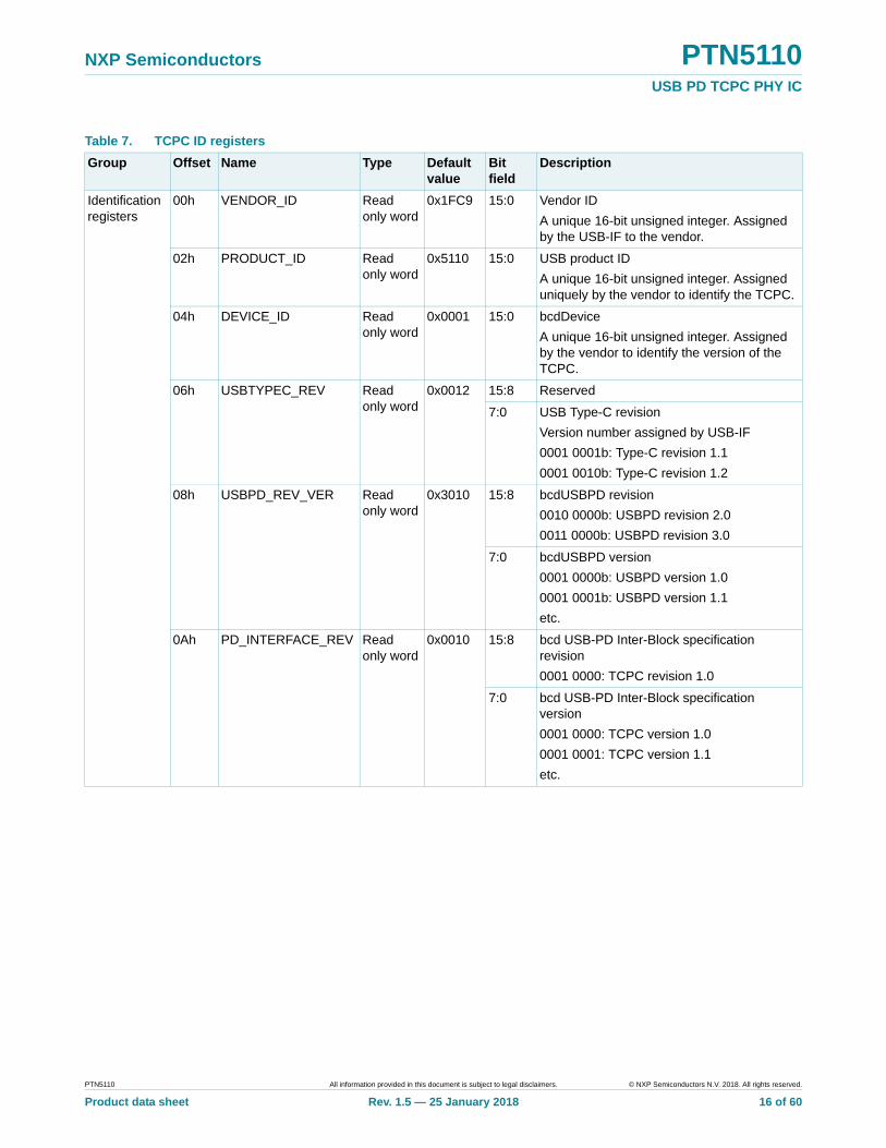
Table 7 describes the TCPC identification registers and their Read only values.
Table 6. I2C slave address
SLV_ADDR pin Device address (Write/read) 7:0
GND 1010000x
10 K pull-up to BYPASS pin 1010001x
Unconnected 1010010x
100 K pull-up to BYPASS pin 1010011x
PTN5110 All information provided in this document is subject to legal disclaimers. © NXP Semiconductors N.V. 2018. All rights reserved.
Product data sheet Rev. 1.5 — 25 January 2018 15 of 60
NXP Semiconductors PTN5110USB PD TCPC PHY IC
Table 7. TCPC ID registers
Group Offset Name Type Default value
Bit field
Description
Identification registers
00h VENDOR_ID Read only word
0x1FC9 15:0 Vendor ID
A unique 16-bit unsigned integer. Assigned by the USB-IF to the vendor.
02h PRODUCT_ID Read only word
0x5110 15:0 USB product ID
A unique 16-bit unsigned integer. Assigned uniquely by the vendor to identify the TCPC.
04h DEVICE_ID Read only word
0x0001 15:0 bcdDevice
A unique 16-bit unsigned integer. Assigned by the vendor to identify the version of the TCPC.
06h USBTYPEC_REV Read only word
0x0012 15:8 Reserved
7:0 USB Type-C revision
Version number assigned by USB-IF
0001 0001b: Type-C revision 1.1
0001 0010b: Type-C revision 1.2
08h USBPD_REV_VER Read only word
0x3010 15:8 bcdUSBPD revision
0010 0000b: USBPD revision 2.0
0011 0000b: USBPD revision 3.0
7:0 bcdUSBPD version
0001 0000b: USBPD version 1.0
0001 0001b: USBPD version 1.1
etc.
0Ah PD_INTERFACE_REV Read only word
0x0010 15:8 bcd USB-PD Inter-Block specification revision
0001 0000: TCPC revision 1.0
7:0 bcd USB-PD Inter-Block specification version
0001 0000: TCPC version 1.0
0001 0001: TCPC version 1.1
etc.
PTN5110 All information provided in this document is subject to legal disclaimers. © NXP Semiconductors N.V. 2018. All rights reserved.
Product data sheet Rev. 1.5 — 25 January 2018 16 of 60

NXP Semiconductors PTN5110USB PD TCPC PHY IC
7.6 Power management and power supplies
PTN5110 is designed to operate under a wide range of VDD and VBUS supply voltages. It can seamlessly transition from VBUS to VDD and vice versa.
Under dead battery operation, PTN5110 applies voltage clamps to both CC pins so that the system may receive power as a Sink. To support platforms with buck-boost configuration, PTN5110 asserts EN_SNK1 pin based on validity of VBUS voltage (facilitates 5 V VBUS sinking).
The following table highlights the power supplies and operating conditions for PTN5110.
The relevant pins associated with this block are:
• VDD
• BYPASS: This is an internal voltage node
• VBUS: This is a connector side pin
PTN5110 provides power management support to conserve power consumption in both Type-C unattached and attached conditions. It supports sleep and wake-up features as per [3].
Table 8. Power supplies versus operating conditions
Valid Power supply Input combination
Operational condition Remarks
VDD Operation under dead and normal battery conditions
PTN5110 is operational. But the host I2C-bus interface and open drain GPIOs can be accessed after open drain pull-up voltage (to VDD) is available only
VBUS, VDD Normal powered condition (both battery based or non-battery based platforms)
PTN5110 and its interfaces are operational. But the host I2C-bus interface and open drain GPIOs can be accessed after open drain pull-up voltage (to VDD) is available only
PTN5110 All information provided in this document is subject to legal disclaimers. © NXP Semiconductors N.V. 2018. All rights reserved.
Product data sheet Rev. 1.5 — 25 January 2018 17 of 60
NXP Semiconductors PTN5110USB PD TCPC PHY IC
8. Use case view
Given that USB Power Delivery could address the requirements of a wide set of markets and product segments, PTN5110 is designed to work over a range of product categories, platform applications, use cases and usage roles. With its configurability, it can serve the needs of both general and custom applications. Not limited to these but the following subsections illustrate a set of example use cases of PTN5110. However, note that these use case diagrams do not capture all the details of schematic reference designs. For instance, ESD/TVS protection diodes are not captured. Please contact NXP for more information in this regard.
PTN5110 All information provided in this document is subject to legal disclaimers. © NXP Semiconductors N.V. 2018. All rights reserved.
Product data sheet Rev. 1.5 — 25 January 2018 18 of 60

NXP Semiconductors PTN5110USB PD TCPC PHY IC
8.1 System use case
8.1.1 USB PD DRP (Provider/Consumer): Notebook PC with buck boost charger
In this illustration, PTN5110 along with EC (with its TCPM) is behind the Type-C receptacle and they are configured as a PD DRP (Provider/Consumer). The EC interfaces with the Charger IC to configure at specific voltage/ current levels to perform battery charging and/or powering of the platform.
This application is expected to:
Fig 4. Illustrative diagram of Notebook/Ultrabook/Tablet application (Separate source and sink power paths): PD Provider/Consumer role (Source role under Normal power/battery; Sink role under dead battery condition)
aaa-022984
TYPE-CCONNECTOR
VBUSV
DD
IO
VBUSDBG_ACC
VINE
N_S
NK
1
FAU
LT_N
EN
_SR
C
BYPASS
5 V REG
NX20P5090(20 V/5 A power switch)
NX5P3290(5 V/3 A power switch)
PTN5110(TCPC PD PHY)
CBTL08GP053(TYPE-C HIGH
SPEED SWITCHFOR USB 3.1,4-LANE DP1.3
AND AUXSIDEBAND)
CC1
TX1+/-
RX1+/-
TX2+/-
RX2+/-
RFU1/2
D+/-
SLV_ADDR VDDIO
VDDIO
RADP
I2C_SCL,I2C_SDA
ALERT_N
VCONN_IN
AUX+/- CPU
HPD
VDD
DP(3:0)+/-
USB3 TX+/-
USB3 RX+/-
USB2+/-
I2C
CC2
FRS
_EN
ILIM
_5V
_VB
US
PCH
TCPMMCU
(PD POLICYAND ALT
MODECONTROLLER)
EC/SMC
SPI
I2C
POWERNETWORK
BATTERY
BUCKBOOST
CHARGERIC
IADP-IADP+
PTN5110 All information provided in this document is subject to legal disclaimers. © NXP Semiconductors N.V. 2018. All rights reserved.
Product data sheet Rev. 1.5 — 25 January 2018 19 of 60
NXP Semiconductors PTN5110USB PD TCPC PHY IC
• Source VBUS 5 V (if not under dead battery)
• Charge from VBUS PD and AC barrel power, if applicable
• Source VCONN power
The EC communicates with PTN5110 via an I2C-bus interface and controls the operations.
An important aspect to note here is that PTN5110 would indicate a 'Rd' pull-down (Sink) under dead battery condition and this enables the port partner to provide VBUS @ 5 V (provided the port partner is capable of acting as Source). However, after system starts up, role swap may be performed to become Source and/or DFP. This is handled by PTN5110 and TCPM together.
DBG_ACC, ILIM_5V_VBUS and FRS_EN pins can be used by the platform, as necessary.
For this application context, it is recommended to use PTN5110HQ version of the IC. There is a consideration for making this recommendation here - buck boost charger power path is assumed to take longer time than that of PTN5110 VBUS debounce time of 15 ms.
If the VDD becomes available before VBUS debounce time of PTN5110, it is suggested to use PTN5110DHQ version.
PTN5110 All information provided in this document is subject to legal disclaimers. © NXP Semiconductors N.V. 2018. All rights reserved.
Product data sheet Rev. 1.5 — 25 January 2018 20 of 60

NXP Semiconductors PTN5110USB PD TCPC PHY IC
8.1.2 USB PD DRP (Provider/Consumer): Notebook PC with regular NVDC charger
Fig 5. Illustrative diagram of Notebook/Ultrabook/Tablet application (Separate source and sink power paths): PD Provider/Consumer role (Source role under Normal power/battery; Sink role under dead battery condition); NVDC charger configuration relying on VBUS LDO for TCPM start up under dead battery
aaa-022985
TYPE-CCONNECTOR
VBUSV
DD
IO
VBUSDBG_ACC
VIN
EN
_SN
K1
FAU
LT_N
EN
_SR
C
BYPASS
5 V REG
NX20P5090(20 V/5 A power switch)
NX5P3290(5 V/3 A power switch)
PTN5110(TCPC PD PHY)
CBTL08GP053(TYPE-C HIGH
SPEED SWITCHFOR USB 3.1,4-LANE DP1.3
AND AUXSIDEBAND)
CC1
TX1+/-
RX1+/-
TX2+/-
RX2+/-
RFU1/2
D+/-
VDDIO
RADP
I2C
ALERT_N
VCONN_IN
AUX+/- CPU
HPD
VDD
DP[3:0]+/-
USB3 TX+/-
USB3 RX+/-
USB2+/-
I2C
CC2
ILIM
_5V
_VB
US
FRS
_EN
SLV
_AD
DR
PCH
TCPMMCU
(PD POLICYAND ALT
MODECONTROLLER)
EC/SMC
SPI
I2C
POWERNETWORK
BATTERY
NVDCCHARGER
IADP-IADP+
VBUSLDO
PTN5110 All information provided in this document is subject to legal disclaimers. © NXP Semiconductors N.V. 2018. All rights reserved.
Product data sheet Rev. 1.5 — 25 January 2018 21 of 60
NXP Semiconductors PTN5110USB PD TCPC PHY IC
In this configuration, NVDC charger IC is used. To support operation on dead battery, a separate VBUS LDO that provides initial current to start up TCPM and charger IC is utilized.
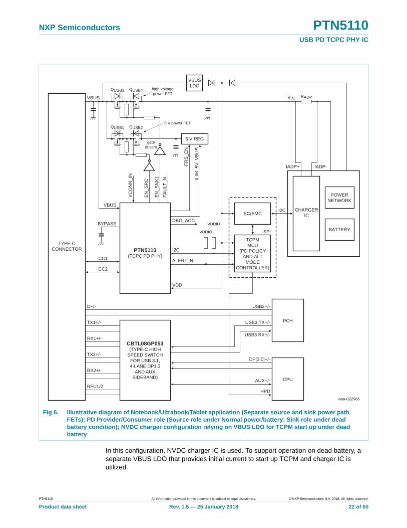
Fig 6. Illustrative diagram of Notebook/Ultrabook/Tablet application (Separate source and sink power path FETs): PD Provider/Consumer role (Source role under Normal power/battery; Sink role under dead battery condition); NVDC charger configuration relying on VBUS LDO for TCPM start up under dead battery
aaa-022986
TYPE-CCONNECTOR
VBUS
VBUS
DBG_ACC
FRS
_EN
FAU
LT_N
gatedrivers
QUSB3 QUSB4
QUSB1 QUSB2
EN
_SN
K1
EN
_SR
C
VC
ON
N_I
N
ILIM
_5V
_VB
US
VIN
BYPASS
5 V REG
PTN5110(TCPC PD PHY)
CBTL08GP053(TYPE-C HIGH
SPEED SWITCHFOR USB 3.1,4-LANE DP1.3
AND AUXSIDEBAND)
VBUSLDO
high voltagepower FET
5 V power FET
CC1
TX1+/-
RX1+/-
TX2+/-
RX2+/-
RFU1/2
D+/-
VDDIO
VDDIO
RADP
I2C
ALERT_N
AUX+/- CPU
HPD
VDD
DP[3:0]+/-
USB3 TX+/-
USB3 RX+/-
USB2+/-
CC2
PCH
TCPMMCU
(PD POLICYAND ALT
MODECONTROLLER)
EC/SMC
SPI
I2C
POWERNETWORK
BATTERY
CHARGERIC
IADP-IADP+
PTN5110 All information provided in this document is subject to legal disclaimers. © NXP Semiconductors N.V. 2018. All rights reserved.
Product data sheet Rev. 1.5 — 25 January 2018 22 of 60
NXP Semiconductors PTN5110USB PD TCPC PHY IC
Figure 5 illustrates the use case using load switches whereas Figure 6 illustrates the same with FETs. It should be noted that in Figure 6, gate drivers are required to drive the MOSFETs.
For this application context, it is recommended to use PTN5110DHQ version of the IC. There is a consideration for making this recommendation here - VBUS LDO regulator power path is assumed to start providing VDD earlier than PTN5110 VBUS debounce time of 15 ms.
If the VDD becomes available later than VBUS debounce time of PTN5110, it is feasible to to use PTN5110HQ version.
PTN5110 All information provided in this document is subject to legal disclaimers. © NXP Semiconductors N.V. 2018. All rights reserved.
Product data sheet Rev. 1.5 — 25 January 2018 23 of 60

NXP Semiconductors PTN5110USB PD TCPC PHY IC
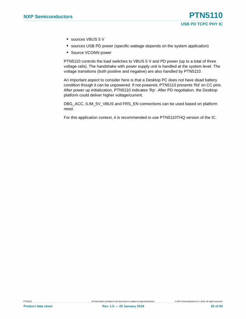
8.1.3 USB PD Source (Provider) with Type-C receptacle: Desktop PC
In this illustration also, PTN5110 and Policy controller & Alternate mode control MCU are behind Type-C receptacle and they are configured to act as a PD Provider (Autonomous mode) based on pre-configured Power profiles. The PC system uses the ATX or similar power supply and it can deliver power to all USB ports. In this diagram, there is no EC to interface with and so, the solution (TCPM MCU and PTN5110) is configured for autonomous operation.
For USB ports, this application:
Fig 7. Illustrative diagram of Desktop PC application (2 Source power paths): PD Provider only (Source role under powered condition)
aaa-022987
TYPE-CCONNECTOR
VBUS
VD
DIO
VBUS
DBG_ACC
EN
_SN
K1
FAU
LT_N
EN
_US
BS
RC
BYPASS
5 V REG
high voltage VBUSsource power switch
NX5P3090/NX5P3290(5 V/3 A power switch)
PTN5110(TCPC PD PHY)
CBTL08GP053(TYPE-C HIGH
SPEED SWITCHFOR USB 3.1,4-LANE DP1.3
AND AUXSIDEBAND)
CC1
TX1+/-
RX1+/-
TX2+/-
RX2+/-
RFU1/2
D+/-
VCONN_IN
SLV_ADDRVDDIO
VDDIO
I2C
ALERT_N
AUX+/- CPU
HPD
VDD
DP[3:0]+/-
USB3 TX+/-
USB3 RX+/-
USB2+/-
I2C
CC2
ILIM
_5V
_VB
US
FRS
_EN
PCH
TCPM(PD POLICY
AND ALTMODE
CONTROLLER)
controlGPIO
PLATFORMPOWER
NETWORK
PTN5110 All information provided in this document is subject to legal disclaimers. © NXP Semiconductors N.V. 2018. All rights reserved.
Product data sheet Rev. 1.5 — 25 January 2018 24 of 60
NXP Semiconductors PTN5110USB PD TCPC PHY IC
• sources VBUS 5 V
• sources USB PD power (specific wattage depends on the system application)
• Source VCONN power
PTN5110 controls the load switches to VBUS 5 V and PD power (up to a total of three voltage rails). The handshake with power supply unit is handled at the system level. The voltage transitions (both positive and negative) are also handled by PTN5110.
An important aspect to consider here is that a Desktop PC does not have dead battery condition though it can be unpowered. If not powered, PTN5110 presents 'Rd' on CC pins. After power up initialization, PTN5110 indicates 'Rp'. After PD negotiation, the Desktop platform could deliver higher voltage/current.
DBG_ACC, ILIM_5V_VBUS and FRS_EN connections can be used based on platform need.
For this application context, it is recommended to use PTN5110THQ version of the IC.
PTN5110 All information provided in this document is subject to legal disclaimers. © NXP Semiconductors N.V. 2018. All rights reserved.
Product data sheet Rev. 1.5 — 25 January 2018 25 of 60

NXP Semiconductors PTN5110USB PD TCPC PHY IC
8.1.4 USB PD DRP (Provider/Consumer: Smartphone use case) Standalone PTN5110
In this illustration, PTN5110 is behind Type-C receptacle and it is configured to act as a PD Provider/ Consumer. It is important to note that there is no dedicated policy controller MCU associated with the PD functionality (but Application is used to serve the purpose). Under normal battery/powered condition, PTN5110 is configured as DRP (with Try.SNK
Fig 8. Illustrative diagram of Low power devices (e.g. Smartphones) that need 5 V, 3 A only: PD Provider/Consumer (Source role with Sink in dead battery condition and Source/Sink role depending on Type-C Partner capability. The PMIC is assumed to have buck-boost configuration
aaa-022988
TYPE-CCONNECTOR
VBUS
EN
_SR
C
EN
_SN
KD
B
SLV
_AD
DR
FAU
LT_N
BYPASS
load switch(bi-directional)
PTN5110(TCPC PD PHY)
CBTL08GP053(TYPE-C HIGH
SPEED SWITCH
CC1
TX1
RX1
TX2
RX2
RFU1/2
USB2
VDDIO
ALERT_N
SLV_ADDR
I2C
VCONN_IN
DBG_ACC
AUX+/-
4-lane DP
VDD
USB3 TX
USB3 RX
I2C
CC2
FRS
_EN
ILIM
_5V
_VB
US
APPLICATIONPROCCESSOR
POWERSYSTEM
IBAT-
QBATT
VBATT
IBAT+
VDC
RBATT
CCHR_OUT
CCHR_INQCHR_SW
QCHR_SYN
SYSTEMPMIC WITHCHARGER
CONTROLLER
BATTERY
QBATT
PTN5110 All information provided in this document is subject to legal disclaimers. © NXP Semiconductors N.V. 2018. All rights reserved.
Product data sheet Rev. 1.5 — 25 January 2018 26 of 60
NXP Semiconductors PTN5110USB PD TCPC PHY IC
preference) and it performs cable/plug connect and disconnect detection, orientation detection (Application Processor must determine orientation). However, on dead battery condition, it defaults to 'Rd'/Sink role.
The power path control signals (EN_SNK1, EN_SRC) handle power flow in one direction each:
• when operating as a Sink, this use case using EN_SNK1 supports charging of the platform and
• when in Source, EN_SRC supports power path control of VBUS 5V to the Type-C peripheral.
This application is expected to:
• Sourcing VCONN power is dependent on the Type-C data role taken
The Application processor implements PD and Alt mode functionality.
DBG_ACC, ILIM_5V_VBUS and FRS_EN connections can be used based on platform need.
For this application context, it is recommended to use PTN5110HQ version of the IC. There is a consideration for making this recommendation here - System PMIC power path is assumed to take longer time than that of PTN5110 VBUS debounce time of 15 ms.
If the VDD becomes available before VBUS debounce time of PTN5110, it is suggested to use PTN5110DHQ version.
PTN5110 All information provided in this document is subject to legal disclaimers. © NXP Semiconductors N.V. 2018. All rights reserved.
Product data sheet Rev. 1.5 — 25 January 2018 27 of 60

NXP Semiconductors PTN5110USB PD TCPC PHY IC
8.1.5 Type-C adapters with PTN5110
In this illustration, PTN5110 is inside Type-C cable adapter operating in Sink role. Some example use cases are Type-C to DP adapter, Type-C to VGA adapter, Type-C to Thunderbolt adapter etc. PTN5110 serves as PD PHY layer device for a Cable adapter management MCU or dedicated PD MCU wherein PD policy management, Alternate mode and VDM support are handled. The USB Billboard device is assumed to be implemented as part of adapter management MCU.
The cable adapter implementation operates on VCONN supply. Discrete depletion mode FET can be used in the application for 'Ra' indication on CC pin.
For this application context, it is recommended to use PTN5110DHQ version of the IC.
Fig 9. Illustrative diagram of Cable adapter use case (e.g. Sink in a Type-C to legacy adapter)
aaa-022989
TYPE-CPLUG
INTERFACECONNECTOR
VBUS
VCONNDCDC
depletionmode FET Ra
PTN5110(PD PHY)
ADAPTER/DONGLE HIGHSPEED CIRCUITRY
-SWITCHING AND/ORPROTOCOL CONVERTER
TX1+/-
RX1+/-
TX2+/-
RX2+/-
RFU1/2
D+/-
CC1
VDDIO
I2C
ALERT_N
USB2+/-
VDD VBUS VDD
LPC11xxxADAPTER MCU
(TCPMIMPLEMENTS
PD POLICY ANDALTERNATE MODE
SUPPORT
USB BB
interfacesignals
PTN5110 All information provided in this document is subject to legal disclaimers. © NXP Semiconductors N.V. 2018. All rights reserved.
Product data sheet Rev. 1.5 — 25 January 2018 28 of 60
NXP Semiconductors PTN5110USB PD TCPC PHY IC
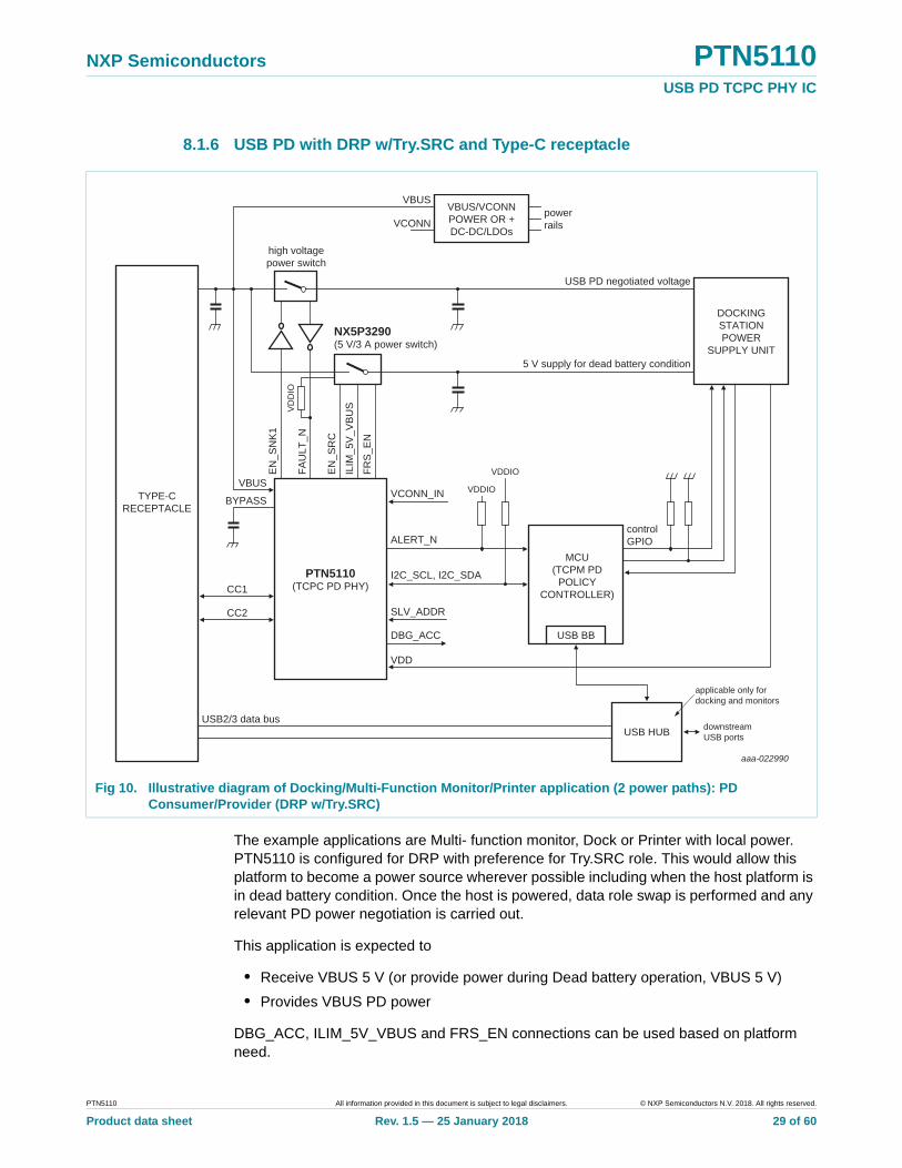
8.1.6 USB PD with DRP w/Try.SRC and Type-C receptacle
The example applications are Multi- function monitor, Dock or Printer with local power. PTN5110 is configured for DRP with preference for Try.SRC role. This would allow this platform to become a power source wherever possible including when the host platform is in dead battery condition. Once the host is powered, data role swap is performed and any relevant PD power negotiation is carried out.
This application is expected to
• Receive VBUS 5 V (or provide power during Dead battery operation, VBUS 5 V)
• Provides VBUS PD power
DBG_ACC, ILIM_5V_VBUS and FRS_EN connections can be used based on platform need.
Fig 10. Illustrative diagram of Docking/Multi-Function Monitor/Printer application (2 power paths): PD Consumer/Provider (DRP w/Try.SRC)
aaa-022990
TYPE-CRECEPTACLE
VD
DIO
VBUS
EN
_SN
K1
FAU
LT_N
EN
_SR
C
BYPASS
high voltagepower switch
NX5P3290(5 V/3 A power switch)
PTN5110(TCPC PD PHY)CC1
USB2/3 data bus
DBG_ACC
SLV_ADDR
VDDIO
VDDIO
ALERT_N
I2C_SCL, I2C_SDA
VCONN_IN
VDD
CC2
ILIM
_5V
_VB
US
FRS
_EN
DOCKINGSTATIONPOWER
SUPPLY UNIT
USB HUB
USB BB
MCU(TCPM PD
POLICYCONTROLLER)
VBUS/VCONNPOWER OR +DC-DC/LDOs
powerrails
VBUS
VCONN
USB PD negotiated voltage
5 V supply for dead battery condition
controlGPIO
applicable only fordocking and monitors
downstreamUSB ports
PTN5110 All information provided in this document is subject to legal disclaimers. © NXP Semiconductors N.V. 2018. All rights reserved.
Product data sheet Rev. 1.5 — 25 January 2018 29 of 60
NXP Semiconductors PTN5110USB PD TCPC PHY IC
For this application context, it is recommended to use PTN5110DHQ version of the IC.
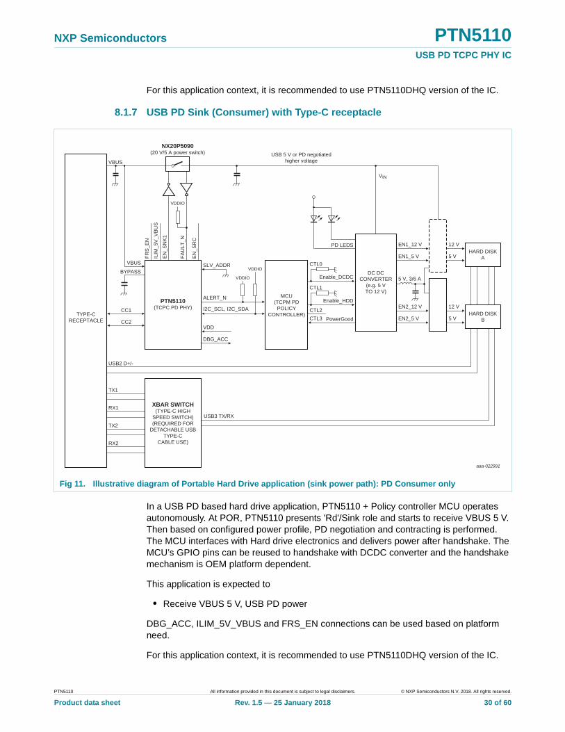
8.1.7 USB PD Sink (Consumer) with Type-C receptacle
In a USB PD based hard drive application, PTN5110 + Policy controller MCU operates autonomously. At POR, PTN5110 presents 'Rd'/Sink role and starts to receive VBUS 5 V. Then based on configured power profile, PD negotiation and contracting is performed. The MCU interfaces with Hard drive electronics and delivers power after handshake. The MCU’s GPIO pins can be reused to handshake with DCDC converter and the handshake mechanism is OEM platform dependent.
This application is expected to
• Receive VBUS 5 V, USB PD power
DBG_ACC, ILIM_5V_VBUS and FRS_EN connections can be used based on platform need.
For this application context, it is recommended to use PTN5110DHQ version of the IC.
Fig 11. Illustrative diagram of Portable Hard Drive application (sink power path): PD Consumer only
aaa-022991
TYPE-CRECEPTACLE
VBUS
VDDIO
VBUS
DBG_ACC
USB 5 V or PD negotiatedhigher voltage
VIN
EN
_SN
K1
FAU
LT_N
EN
_SR
C
BYPASS
NX20P5090(20 V/5 A power switch)
PTN5110(TCPC PD PHY)
XBAR SWITCH(TYPE-C HIGH
SPEED SWITCH)(REQUIRED FOR
DETACHABLE USBTYPE-C
CABLE USE)
CC1
TX1
RX1USB3 TX/RX
TX2
RX2
USB2 D+/-
EN1_12 V
EN1_5 V
5 V, 3/6 A
12 V
5 V
12 V
5 V
EN2_12 V
EN2_5 V
SLV_ADDR
VDDIO
VDDIO
ALERT_N
PowerGood
CTL2CTL3
Enable_HDD
CTL1
Enable_DCDC
CTL0
I2C_SCL, I2C_SDA
VDDCC2
FRS
_EN
ILIM
_5V
_VB
US
MCU(TCPM PD
POLICYCONTROLLER)
DC DCCONVERTER
(e.g. 5 VTO 12 V)
PD LEDSHARD DISK
A
HARD DISKB
PTN5110 All information provided in this document is subject to legal disclaimers. © NXP Semiconductors N.V. 2018. All rights reserved.
Product data sheet Rev. 1.5 — 25 January 2018 30 of 60
NXP Semiconductors PTN5110USB PD TCPC PHY IC
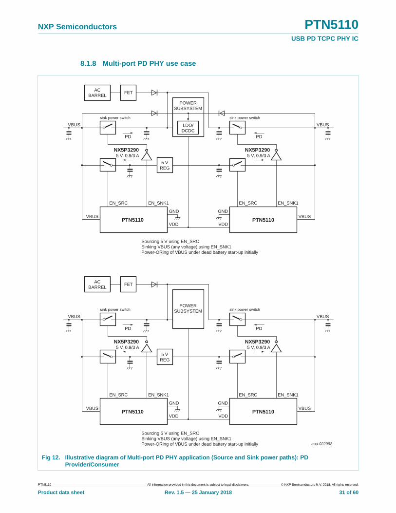
8.1.8 Multi-port PD PHY use case
Fig 12. Illustrative diagram of Multi-port PD PHY application (Source and Sink power paths): PD Provider/Consumer
aaa-022992
PTN5110
ACBARREL
5 VREG
sink power switch
PD
VBUS
NX5P32905 V, 0.9/3 A
NX5P32905 V, 0.9/3 A
EN_SRC
GND
VDD
EN_SNK1
FET
LDO/DCDC
POWERSUBSYSTEM
sink power switch
PD
VBUS
VBUSPTN5110
EN_SRC
GND
VDD
EN_SNK1
Sourcing 5 V using EN_SRCSinking VBUS (any voltage) using EN_SNK1Power-ORing of VBUS under dead battery start-up initially
VBUS
PTN5110
ACBARREL
5 VREG
sink power switch
PD
VBUS
NX5P32905 V, 0.9/3 A
NX5P32905 V, 0.9/3 A
EN_SRC
GND
VDD
EN_SNK1
FET
POWERSUBSYSTEM sink power switch
PD
VBUS
VBUSPTN5110
EN_SRC
GND
VDD
EN_SNK1
Sourcing 5 V using EN_SRCSinking VBUS (any voltage) using EN_SNK1Power-ORing of VBUS under dead battery start-up initially
VBUS
PTN5110 All information provided in this document is subject to legal disclaimers. © NXP Semiconductors N.V. 2018. All rights reserved.
Product data sheet Rev. 1.5 — 25 January 2018 31 of 60
NXP Semiconductors PTN5110USB PD TCPC PHY IC
Two example scenarios are captured in the illustrations. This application can be a typical notebook PC with two-port support. Depending on whether the PC uses Buck boost charger or regular NVDC charger, the platform implementation would be different.
For this application context, it is recommended to use PTN5110HQ version of the IC. There is a consideration for making this recommendation here - power subsystem is assumed to take longer time than that of PTN5110 VBUS debounce time of 15 ms.
If the VDD becomes available before VBUS debounce time of PTN5110, it is suggested to use PTN5110DHQ version.
PTN5110 All information provided in this document is subject to legal disclaimers. © NXP Semiconductors N.V. 2018. All rights reserved.
Product data sheet Rev. 1.5 — 25 January 2018 32 of 60

NXP Semiconductors PTN5110USB PD TCPC PHY IC
9. Limiting values
[1] All voltage values, except differential voltages, are with respect to network ground terminal.
[2] Human Body Model: ANSI/ESDA/JEDEC JDS-001-2012 (Revision of ANSI/ESDA/JEDEC JS-001-2011), ESDA/JEDEC Joint standard for ESD sensitivity testing, Human Body Model - Component level; Electrostatic Discharge Association, Rome, NY, USA; JEDEC Solid State Technology Association, Arlington, VA, USA.
[3] Charged Device Model: JESD22-C101E December 2009 (Revision of JESD22-C101D, October 2008), standard for ESD sensitivity testing, Charged Device Model - Component level; JEDEC Solid State Technology Association, Arlington, VA, USA.
[4] Specification valid only with respect to pins other than VBUS, CC1 and CC2.
Table 9. Limiting valuesIn accordance with the Absolute Maximum Rating System (IEC 60134).
Symbol Parameter Conditions Min Max Unit
VDD Supply voltage 0.5 +6.0 V
VBUS USB VBUS voltage 0.5 +28 V
Vpullup I2C pull-up voltage Applies to I2C_SCL, I2C_SDA
0.5 +5.5 V
VI Input voltage voltage at the pin
CC1, CC2 0.5 +6.0 V
EN_SRC, EN_SNK1 0.5 +4.6 V
BYPASS 0.5 +2.5 V
VCONN_IN 0.5 +6.0 V
ALERT_N 0.5 +4.6 V
ILIM_5V_VBUS
DBG_ACC, FRS_EN, FAULT_N
0.5 +4.6 V
SLV_ADDR 0.5 +4.6 V
I2C_SCL, I2C_SDA 0.5 +4.6 V
Tstg Storage temperature 65 +150 C
VESD electrostatic discharge voltage
HBM –VBUS, CC1, CC2
8000 - V
HBM for other pins[4] 2000 V
CDM 1000 - V
PTN5110 All information provided in this document is subject to legal disclaimers. © NXP Semiconductors N.V. 2018. All rights reserved.
Product data sheet Rev. 1.5 — 25 January 2018 33 of 60
NXP Semiconductors PTN5110USB PD TCPC PHY IC
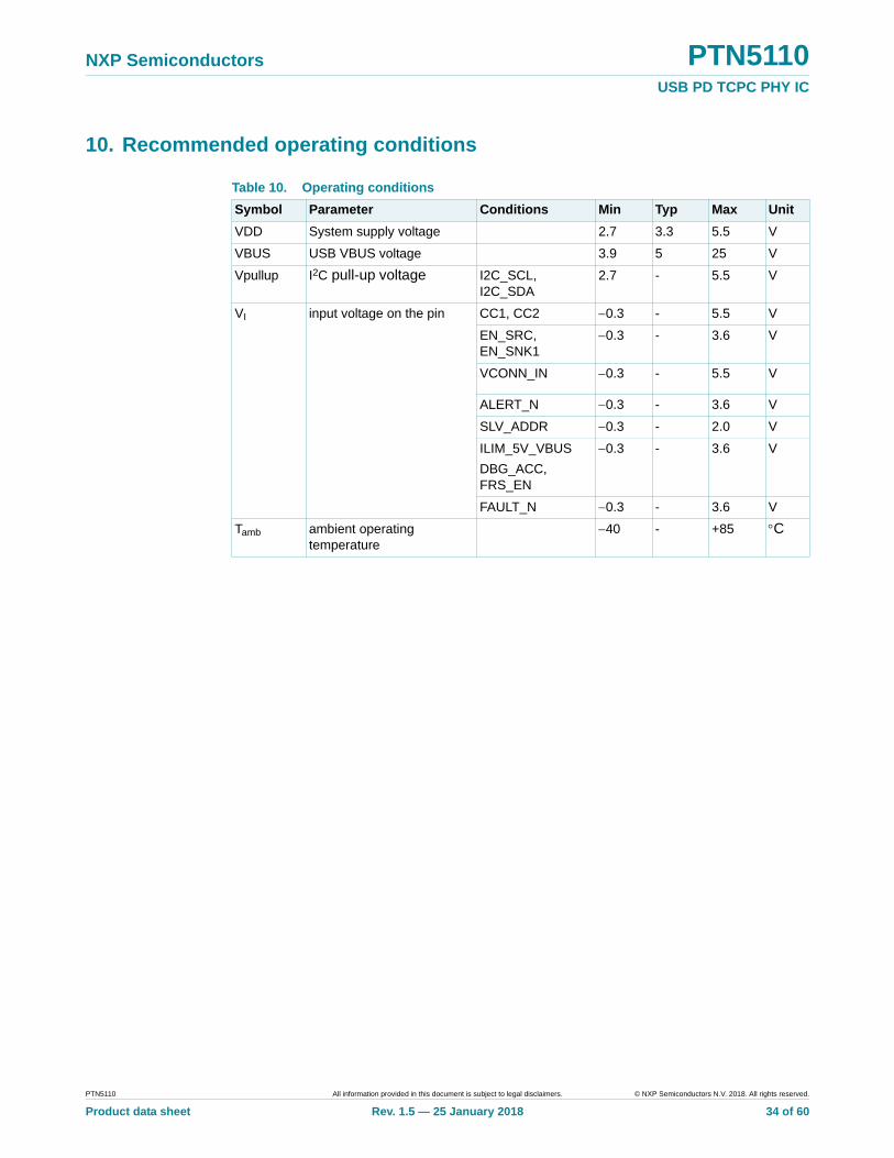
10. Recommended operating conditions
Table 10. Operating conditions
Symbol Parameter Conditions Min Typ Max Unit
VDD System supply voltage 2.7 3.3 5.5 V
VBUS USB VBUS voltage 3.9 5 25 V
Vpullup I2C pull-up voltage I2C_SCL, I2C_SDA
2.7 - 5.5 V
VI input voltage on the pin CC1, CC2 0.3 - 5.5 V
EN_SRC, EN_SNK1
0.3 - 3.6 V
VCONN_IN 0.3 - 5.5 V
ALERT_N 0.3 - 3.6 V
SLV_ADDR 0.3 - 2.0 V
ILIM_5V_VBUS
DBG_ACC, FRS_EN
0.3 - 3.6 V
FAULT_N 0.3 - 3.6 V
Tamb ambient operating temperature
40 - +85 C
PTN5110 All information provided in this document is subject to legal disclaimers. © NXP Semiconductors N.V. 2018. All rights reserved.
Product data sheet Rev. 1.5 — 25 January 2018 34 of 60
NXP Semiconductors PTN5110USB PD TCPC PHY IC
11. Characteristics
11.1 Device characteristics
Table 11. Device characteristicsApplicable across operating temperature and power supply ranges as per Section 10 “Recommended operating conditions” (unless otherwise noted); Typical values are specified at 27C (unless otherwise noted); all leakage currents are specified when VDD = 0 (GND) /VBUS = 0 (GND) = GND
Symbol Parameter Conditions Min Typ Max Unit
IDD,Active Active mode operating current on VDD
Sink role; attached condition; I2C Clock stretching is enabled on TCPCi interface; VBUS ADC not enabled; VBUS monitoring not enabled; VCONN switch not enabled
- 0.55 0.7 mA
Source role; attached condition; 3 A current advertisement; I2C Clock stretching is enabled on TCPCi interface
- 0.8 1 mA
Only when PD mode is functional (packet transmission is in progress; this is PD peak current and not steady state current)
- 6.3 8 mA
Additional current consumed on VDD
VCONN switch is enabled with OCL and RVP; excluding VCONN current flow
- 105 250 A
Current drawn on VBUS under dead battery condition
Sink role, VBUS = 5 V, VDD = 0 - 145 - A
Current drawn on VDD for VBUS monitoring, measurement, etc.
VDD = 3.3 V, VBUS = 3.7 V to 25 V (divided via resistor ladder)
- 500 - A
IDD(idle) Idle mode current on VDD Sink role; Unattached condition; I2C Clock stretching is enabled on TCPCi interface
- 30 - A
Source role; Unattached condition (Rp at standard current level); I2C Clock stretching is enabled on TCPCi interface
- 35 - A
DRP mode; Unattached condition I2C Clock stretching is enabled on TCPCi interface
- 40 - A
Ibckdrv Backdrive current on VDD pin via CC1/2
Backdrive current when VDD = 0, and VBUS = 0
CC1/2 = 5.5 V 10 - 10 A
ILIH,CC HIGH-level input leakage current on a CC pin
Pin voltage = 5.5 V, VDD = 0, VBUS = 0 - - 6 mA
ILIL,CC LOW-level input leakage current on a CC pin
Pin pulled to GND, VDD = 0, VBUS = 0 20 - - A
tFET_EN Time duration between I2C write/ACK response and FET enable asserted
Applicable to all FET control pins - - 50 s
PTN5110 All information provided in this document is subject to legal disclaimers. © NXP Semiconductors N.V. 2018. All rights reserved.
Product data sheet Rev. 1.5 — 25 January 2018 35 of 60
NXP Semiconductors PTN5110USB PD TCPC PHY IC
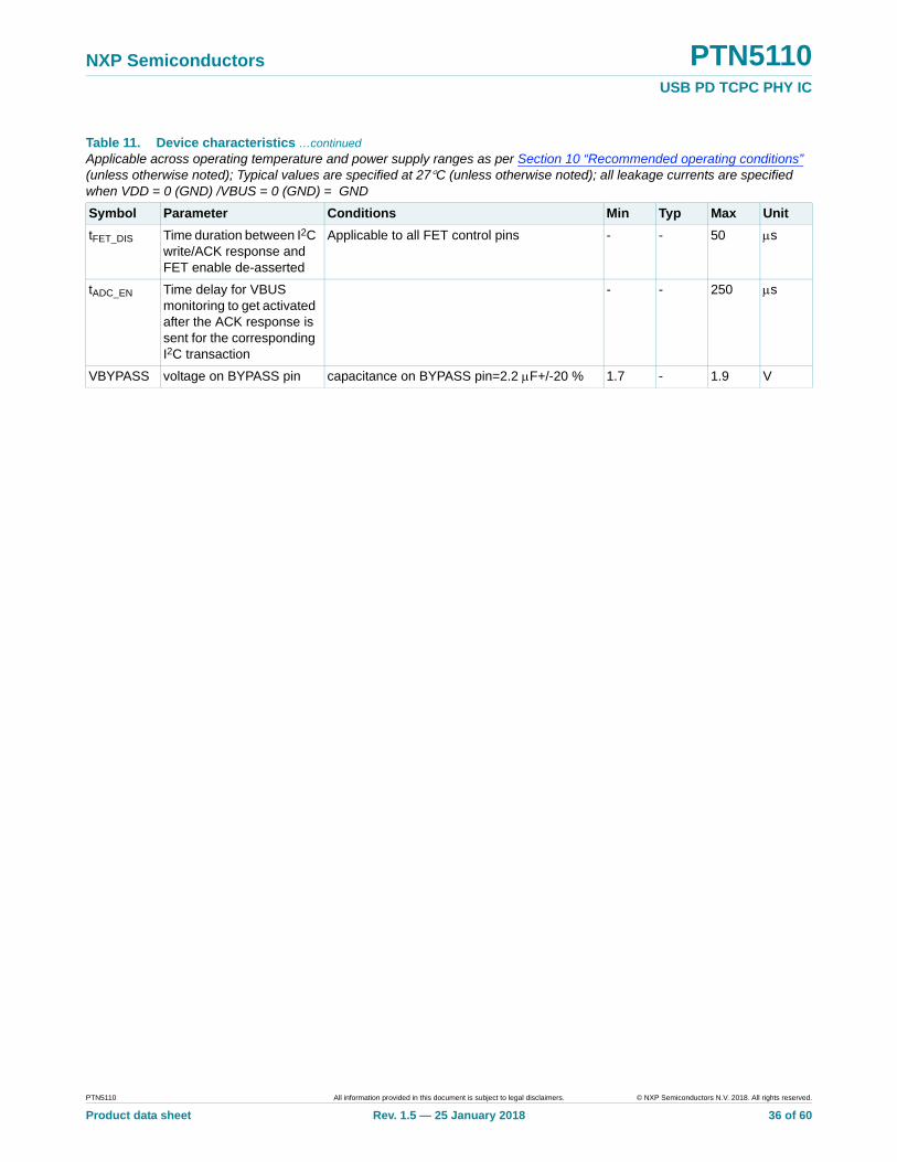
tFET_DIS Time duration between I2C write/ACK response and FET enable de-asserted
Applicable to all FET control pins - - 50 s
tADC_EN Time delay for VBUS monitoring to get activated after the ACK response is sent for the corresponding I2C transaction
- - 250 s
VBYPASS voltage on BYPASS pin capacitance on BYPASS pin=2.2 F+/-20 % 1.7 - 1.9 V
Table 11. Device characteristics …continuedApplicable across operating temperature and power supply ranges as per Section 10 “Recommended operating conditions” (unless otherwise noted); Typical values are specified at 27C (unless otherwise noted); all leakage currents are specified when VDD = 0 (GND) /VBUS = 0 (GND) = GND
Symbol Parameter Conditions Min Typ Max Unit
PTN5110 All information provided in this document is subject to legal disclaimers. © NXP Semiconductors N.V. 2018. All rights reserved.
Product data sheet Rev. 1.5 — 25 January 2018 36 of 60

NXP Semiconductors PTN5110USB PD TCPC PHY IC
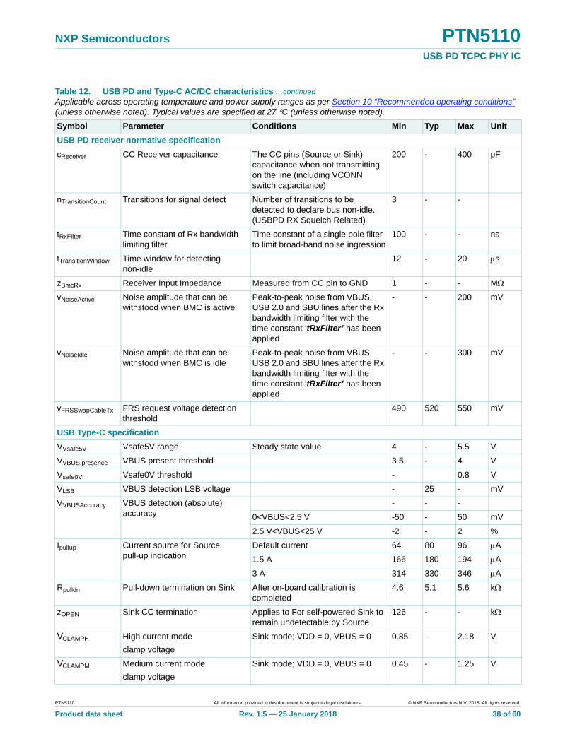
11.2 USB PD and Type-C characteristics
Table 12. USB PD and Type-C AC/DC characteristicsApplicable across operating temperature and power supply ranges as per Section 10 “Recommended operating conditions” (unless otherwise noted). Typical values are specified at 27 C (unless otherwise noted).
Symbol Parameter Conditions Min Typ Max Unit
USB PD normative specification
fBitrate BMC Bit rate 270 300 330 Kbps
tUI Bit Unit Interval 3.03 - 3.7 s
pBitRate Maximum difference between the bit-rate during the payload and the reference bit-rate (The reference bit rate is the average bit rate of the last 32 bits of the preamble)
During transmission - - 0.25 %
tInterFrameGap Time from the end of last bit of a Frame until the start of the first bit of the next Preamble
25 - - s
tStartDrive Time before the start of the first bit of the Preamble when the transmitter shall start driving the line
-1 - 1 s
USB PD transmitter normative specification
tEndDriveBMC Time to cease driving the line after the end of the last bit of the Frame
Min value is limited by tHoldLowBMC - 23 s
tFall Fall time 10 % and 90 % amplitude points, minimum is under unloaded condition
300 - - ns
tHoldLowBMC Time to cease driving the line after the final high-to-low transition
Max value is limited by tEndDriveBMC 1 - - s
tRise Rise time 10 % and 90 % amplitude points, minimum is under unloaded condition
300 - - ns
vSwing Voltage swing 1.05 1.125 1.2 V
TX_ONE “1” level on CC pins during transmitting data
1.05 1.125 1.2 V
TX_ZERO “0” level on CC pins during transmitting data
0 - 0.075 V
zDriver Transmitter output impedance Source output impedance at the Nyquist frequency of [USB2.0] low speed (750 kHz) while the source is driving the CC line.
33 - 75 Ω
rFRSSwapTx FRS request transmit driver resistance (excluding cable resistance)
Maximum driver resistance of a FRS request transmitter
- - 5 Ω
tFRSwapTx FRS request transmit duration FRS request is indicated from the initial Source to the initial Sink by driving CC low for this time
60 - 120 s
PTN5110 All information provided in this document is subject to legal disclaimers. © NXP Semiconductors N.V. 2018. All rights reserved.
Product data sheet Rev. 1.5 — 25 January 2018 37 of 60
NXP Semiconductors PTN5110USB PD TCPC PHY IC
USB PD receiver normative specification
cReceiver CC Receiver capacitance The CC pins (Source or Sink) capacitance when not transmitting on the line (including VCONN switch capacitance)
200 - 400 pF
nTransitionCount Transitions for signal detect Number of transitions to be detected to declare bus non-idle. (USBPD RX Squelch Related)
3 - -
tRxFilter Time constant of Rx bandwidth limiting filter
Time constant of a single pole filter to limit broad-band noise ingression
100 - - ns
tTransitionWindow Time window for detecting non-idle
12 - 20 s
zBmcRx Receiver Input Impedance Measured from CC pin to GND 1 - - M
vNoiseActive Noise amplitude that can be withstood when BMC is active
Peak-to-peak noise from VBUS, USB 2.0 and SBU lines after the Rx bandwidth limiting filter with the time constant ‘tRxFilter’ has been applied
- - 200 mV
vNoiseIdle Noise amplitude that can be withstood when BMC is idle
Peak-to-peak noise from VBUS, USB 2.0 and SBU lines after the Rx bandwidth limiting filter with the time constant ‘tRxFilter’ has been applied
- - 300 mV
vFRSSwapCableTx FRS request voltage detection threshold
490 520 550 mV
USB Type-C specification
VVsafe5V Vsafe5V range Steady state value 4 - 5.5 V
VVBUS,presence VBUS present threshold 3.5 - 4 V
Vsafe0V Vsafe0V threshold - 0.8 V
VLSB VBUS detection LSB voltage - 25 - mV
VVBUSAccuracy VBUS detection (absolute) accuracy
- - -
0<VBUS<2.5 V -50 - 50 mV
2.5 V<VBUS<25 V -2 - 2 %
Ipullup Current source for Source pull-up indication
Default current 64 80 96 A
1.5 A 166 180 194 A
3 A 314 330 346 A
Rpulldn Pull-down termination on Sink After on-board calibration is completed
4.6 5.1 5.6 k
zOPEN Sink CC termination Applies to For self-powered Sink to remain undetectable by Source
126 - - k
VCLAMPH High current mode
clamp voltage
Sink mode; VDD = 0, VBUS = 0 0.85 - 2.18 V
VCLAMPM Medium current mode
clamp voltage
Sink mode; VDD = 0, VBUS = 0 0.45 - 1.25 V
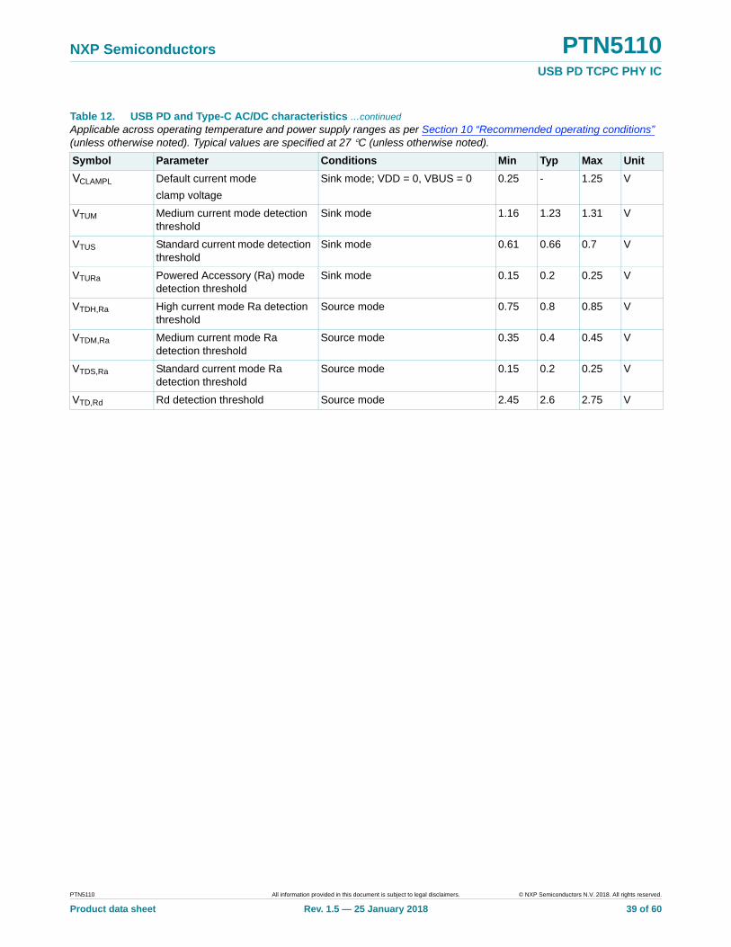
Table 12. USB PD and Type-C AC/DC characteristics …continuedApplicable across operating temperature and power supply ranges as per Section 10 “Recommended operating conditions” (unless otherwise noted). Typical values are specified at 27 C (unless otherwise noted).
Symbol Parameter Conditions Min Typ Max Unit
PTN5110 All information provided in this document is subject to legal disclaimers. © NXP Semiconductors N.V. 2018. All rights reserved.
Product data sheet Rev. 1.5 — 25 January 2018 38 of 60
NXP Semiconductors PTN5110USB PD TCPC PHY IC
VCLAMPL Default current mode
clamp voltage
Sink mode; VDD = 0, VBUS = 0 0.25 - 1.25 V
VTUM Medium current mode detection threshold
Sink mode 1.16 1.23 1.31 V
VTUS Standard current mode detection threshold
Sink mode 0.61 0.66 0.7 V
VTURa Powered Accessory (Ra) mode detection threshold
Sink mode 0.15 0.2 0.25 V
VTDH,Ra High current mode Ra detection threshold
Source mode 0.75 0.8 0.85 V
VTDM,Ra Medium current mode Ra detection threshold
Source mode 0.35 0.4 0.45 V
VTDS,Ra Standard current mode Ra detection threshold
Source mode 0.15 0.2 0.25 V
VTD,Rd Rd detection threshold Source mode 2.45 2.6 2.75 V
Table 12. USB PD and Type-C AC/DC characteristics …continuedApplicable across operating temperature and power supply ranges as per Section 10 “Recommended operating conditions” (unless otherwise noted). Typical values are specified at 27 C (unless otherwise noted).
Symbol Parameter Conditions Min Typ Max Unit
PTN5110 All information provided in this document is subject to legal disclaimers. © NXP Semiconductors N.V. 2018. All rights reserved.
Product data sheet Rev. 1.5 — 25 January 2018 39 of 60

NXP Semiconductors PTN5110USB PD TCPC PHY IC
11.3 USB VBUS and VCONN timing AC/DC characteristics
Table 13. USB VBUS and VCONN timing AC/DC characteristics(*applicable when Autonomous Type-C Connection state machine implementation is selected)
Symbol Parameter Conditions Min Typ Max Unit
t*VBUSSRC_ON Time taken for asserting EN_SRC to source VBUS after Sink is attached
Source role; attached condition; including CC debounce
- - 200 ms
t*VCONNSRC_ON Time duration for providing VCONN on CC pin after EN_SRC is asserted
Source role; attached condition (Ra is detected); VCONN voltage rising to VCONN_IN (min); Load capacitance = 10 F
- - 2 ms
t*VBUSSRC_OFF Time taken for deasserting EN_SRC after Sink is detached
Source role; detached condition - - 0.5 ms
t*VCONNSRC_OFF Time taken for disconnecting VCONN switch after Sink is detached
Source role; detached condition; VCONN reaches below discharge threshold; Load Capacitance = 10 nF
- - 1 ms
tVBUSDISCHG Time taken for VBUS discharge
Source role; Load Capacitance = 200 F max; VBUS pin going from 21.5 V down below Vsafe0V
- - 650 ms
Source role; Load Capacitance = 200 F max; VBUS pin going from 21.5 V down below Vsafe5V (when initial voltage is >5 V)
- - 275 ms
Time taken for VBUS discharge after deasserting FET control when Sink is detached
Sink role; Load Capacitance = 100 F max; VBUS pin going from 21.5 V down below Vsafe0V; disconnect threshold at 17 V
- - 650 ms
Sink role; Load Capacitance = 100 F max; VBUS pin going from 21.5 V down below Vsafe5V (when initial voltage is >5V); disconnect threshold at 17 V
- - 275 ms
tVCONNDISCHG Time taken for VCONN discharge once I2C command for discharging is received
Load Capacitance = 15 F VCONN going down below VVCONNDischarge[2]
- - 30 ms
t*DRP DRP cycle time Unattached condition 50 - 100 ms
t*DRPTry Wait time in Try.SRC state Unattached condition 75 - 150 ms
Duty cycle* (for SRC)
Percentage of time that DRP advertise source during tDRP
Unattached condition 30 - 70 %
t*DRPTransition Time for DRP to complete transition between Source and Sink roles during role resolution
Unattached condition 0 - 1 ms
PTN5110 All information provided in this document is subject to legal disclaimers. © NXP Semiconductors N.V. 2018. All rights reserved.
Product data sheet Rev. 1.5 — 25 January 2018 40 of 60
NXP Semiconductors PTN5110USB PD TCPC PHY IC
11.4 VCONN switch characteristics
Table 14. VCONN switch AC/DC characteristicsApplicable across operating temperature and power supply ranges as per Section 10 “Recommended operating conditions” (unless otherwise noted). Typical values are specified at 27 °C (unless otherwise noted).
Symbol Parameter Conditions Min Typ Max Unit
VVCONN_IN VCONN_IN voltage 2.7 - 5.5 V
IShort Trigger value of Current for raising Short-to-GND fault
0.75 - 2.4 A
RON ON resistance - 350 450 m
CON ON capacitance - 115 - pF
COFF OFF capacitance - 35 - pF
VUVLO Under voltage lockout threshold on VCONN_IN pin
1.7 - 1.9 V
Iinrush Inrush current When VCONN switch is enabled; corresponding CCx pin voltage is zero; CC capacitance = 10 F
- - 100 mA
ICL Current Limiting thresholds @ threshold of 150 mA 100 160 230 mA
@ threshold of 300 mA 230 305 375 mA
@ threshold of 450 mA 375 450 580 mA
@ threshold of 600 mA 500 600 750 mA
Vdischg VCONN Discharge threshold
Discharge resistor removal in Source role - - 0.15 V
VVCONN,present VCONN present threshold - 2.4 2.7 V
IRLCL Reverse Leakage Current from CC to VCONN when switch is not enabled
VCONN = 0; VDD = 2.7 V to 5.5 V - - 3 A
VRVP Reverse Voltage allowed before RVP fault protection is triggered
- 55 100 mV
TOTP Temperature threshold for OTP fault triggering
- 138 - C
tOTP,Cycle Time interval for VCONN switch re-enabling after OTP fault occurrence
450 - 650 ms
tdis Duration to detect and current limit switch due to Short to GND
With HW based control enabled - - 10 S
Duration to detect and disable switch due to OTP fault
With HW based control enabled - - 10 S
Duration to detect and disable switch due to RVP fault
With default fault debounce setting (of 46 s)
- - 100 S
PTN5110 All information provided in this document is subject to legal disclaimers. © NXP Semiconductors N.V. 2018. All rights reserved.
Product data sheet Rev. 1.5 — 25 January 2018 41 of 60

NXP Semiconductors PTN5110USB PD TCPC PHY IC
11.5 I2C characteristics
Table 15. I2C-bus interface: AC/DC characteristicsApplicable across operating temperature and power supply ranges as per Section 10 “Recommended operating conditions” (unless otherwise noted). Typical values are specified at 27 °C (unless otherwise noted).
Symbol Parameter Conditions Min Typ Max Unit
FI2C I2C Clock frequency 0 - 1000 kHz
VIH HIGH-level Input voltage 0.7x Vpullup
- - V
VIL LOW-level Input voltage - - 0.3x Vpullup
V
Vhys Hysteresis of Schmitt trigger inputs
Vpullup > 2 V 0.05x Vpullup
- - V
VOL LOW-level output voltage at 3mA sink current
Vpullup > 2 V 0 - 0.4 V
IOL LOW-level output current VOL =0.4 V;
Standard and Fast modes
3 - - mA
VOL =0.4 V;
Fast mode plus
20 - - mA
VOL =0.6 V;
Fast mode
6 - - mA
IIL LOW-level input current Pin voltage: 0.1xVpullup to 0.9x Vpullup max
-10 - 10 A
CI Capacitance of IO pin - - 10 pF
tHD,STA Hold time (repeated) START condition
Fast mode plus; After this period, the first clock pulse is generated
0.26 - - S
tLOW LOW period of I2C clock Fast mode plus 0.5 - - S
tHIGH HIGH period of I2C clock Fast mode plus 0.26 - - S
tSU,STA Setup time (repeated) START condition
Fast mode plus 0.26 - - S
tHD,DAT Data Hold time Fast mode plus 0 - - S
tSU,DAT Data Setup time Fast mode plus 50 - - ns
tr Rise time of I2C_SCL and I2C_SDA signals
Fast mode plus - - 120 ns
tf Fall time of I2C_SCL and I2C_SDA signals
Fast mode plus - - 120 ns
tSU,STO Setup time for STOP condition Fast mode plus 0.26 - - S
tBUF Bus free time between STOP and START condition
Fast mode plus 0.5 - - S
PTN5110 All information provided in this document is subject to legal disclaimers. © NXP Semiconductors N.V. 2018. All rights reserved.
Product data sheet Rev. 1.5 — 25 January 2018 42 of 60

NXP Semiconductors PTN5110USB PD TCPC PHY IC
[1] Vpullup is external pull-up voltage on SCL and SDA pins. The voltage can be 2.7 V to 5.5 V but is recommended to be same/close to VDD.
tVD,DAT Data valid time Fast mode plus - 0.45 S
tVD,ACK Data valid acknowledge time Fast mode plus - 0.45 S
tSP Pulse width of spikes that must be suppressed by input filter
0 - 50 ns
Table 15. I2C-bus interface: AC/DC characteristics …continuedApplicable across operating temperature and power supply ranges as per Section 10 “Recommended operating conditions” (unless otherwise noted). Typical values are specified at 27 °C (unless otherwise noted).
Symbol Parameter Conditions Min Typ Max Unit
Fig 13. I2C-bus timing diagram
aaa-022993
tf
70 %30 %SDA
tf
70 %30 %
S
tr
70 %30 %
70 %30 %
tHD;DAT
SCL
1 / fSCL
70 %30 %
70 %30 %
tr
tVD;DATtHIGH
9th clocktHD;STA tLOW
tSU;DAT
PTN5110 All information provided in this document is subject to legal disclaimers. © NXP Semiconductors N.V. 2018. All rights reserved.
Product data sheet Rev. 1.5 — 25 January 2018 43 of 60

NXP Semiconductors PTN5110USB PD TCPC PHY IC
11.6 Control I/O characteristics
Table 16. Control I/O characteristicsApplicable across operating temperature and power supply ranges as per Section 10 “Recommended operating conditions” (unless otherwise noted). Typical values are specified at 27 °C (unless otherwise noted).
Symbol Parameter Conditions Min Typ Max Unit
FET Control pins (EN_SRC, EN_SNK1)
VOH HIGH-level Output voltage IOH = 1 mA 1.4 - - V
VOL LOW-level Output voltage IOL = 1 mA - - 0.3 V
CI Capacitance of IO pin - - 20 pF
ILIH HIGH-level leakage current VI = 3.3 V 1 - 10 A
ILIL LOW-level leakage current VI = GND 1 - 1 A
GPIO pins (DBG_ACC, ILIM_5V_VBUS, FRS_EN)
VOH HIGH-level Output voltage IOH = 1 mA BYPASS - 0.3
- - V
VOL LOW-level Output voltage IOL = 1 mA - - 0.3 V
VIH HIGH-level Input voltage 0.7 x BYPASS
- BYPASS V
VIL LOW-level Input voltage - - 0.3 x BYPASS
V
CI Capacitance of IO pin - - 20 pF
ILIH HIGH-level leakage current VI = 3.3 V 1 - 10 A
ILIL LOW-level leakage current VI = GND 1 - 1 A
Open drain IO pin (ALERT_N, FAULT_N) pulled up by 10 k[1]
VOL LOW-level output voltage IOL = 1 mA - - 0.5 V
CI Capacitance of IO pin - - 20 pF
ILIH,EN HIGH-level leakage current VI = 3.6 V, pulled up by 10 k 1 - 10 A
ILIL,EN LOW-level leakage current VI = GND 1 - 1 A
PTN5110 All information provided in this document is subject to legal disclaimers. © NXP Semiconductors N.V. 2018. All rights reserved.
Product data sheet Rev. 1.5 — 25 January 2018 44 of 60

NXP Semiconductors PTN5110USB PD TCPC PHY IC
[1] The pull-up voltage on ALERT_N pin can be 2.7 V to 5.5 V and it is expected to be same/close to VDD
SLV_ADDR pin (input)
VIN, range Input voltage range When GND - 50 mV
CI Capacitance of IO pin - - 20 pF
ILIH,EN HIGH-level leakage current VI = BYPASS;
VDD or VBUS is valid
1 - 1 A
ILIL,EN LOW-level leakage current VI = GND 1 - 1 A
Table 16. Control I/O characteristics …continuedApplicable across operating temperature and power supply ranges as per Section 10 “Recommended operating conditions” (unless otherwise noted). Typical values are specified at 27 °C (unless otherwise noted).
Symbol Parameter Conditions Min Typ Max Unit
PTN5110 All information provided in this document is subject to legal disclaimers. © NXP Semiconductors N.V. 2018. All rights reserved.
Product data sheet Rev. 1.5 — 25 January 2018 45 of 60

NXP Semiconductors PTN5110USB PD TCPC PHY IC
12. Package outline
Fig 14. Package outline SOT1883-1 (HX2QFN16)
PTN5110 All information provided in this document is subject to legal disclaimers. © NXP Semiconductors N.V. 2018. All rights reserved.
Product data sheet Rev. 1.5 — 25 January 2018 46 of 60
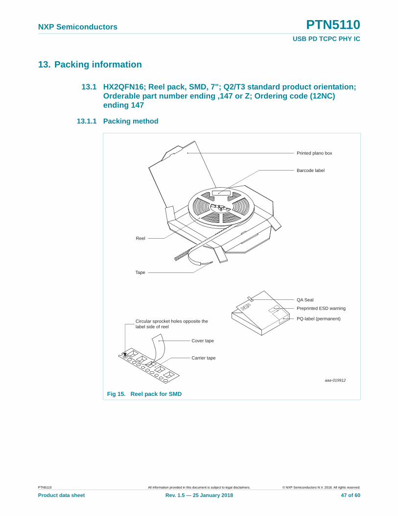
NXP Semiconductors PTN5110USB PD TCPC PHY IC
13. Packing information
13.1 HX2QFN16; Reel pack, SMD, 7"; Q2/T3 standard product orientation; Orderable part number ending ,147 or Z; Ordering code (12NC) ending 147
13.1.1 Packing method
Fig 15. Reel pack for SMD
Cover tape
Circular sprocket holes opposite thelabel side of reel
Carrier tape
aaa-019912
QA Seal
Tape
Reel
Barcode label
Printed plano box
Preprinted ESD warning
PQ-label (permanent)
PTN5110 All information provided in this document is subject to legal disclaimers. © NXP Semiconductors N.V. 2018. All rights reserved.
Product data sheet Rev. 1.5 — 25 January 2018 47 of 60
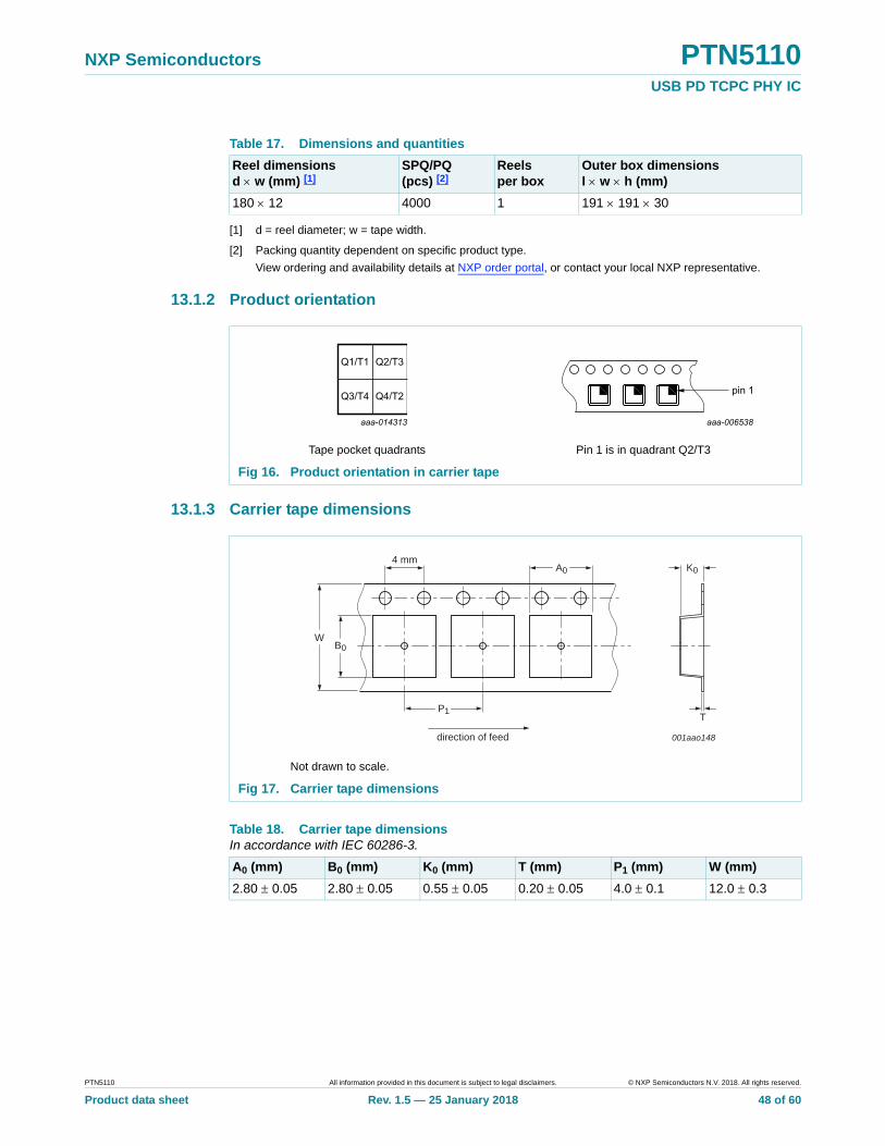
NXP Semiconductors PTN5110USB PD TCPC PHY IC
[1] d = reel diameter; w = tape width.
[2] Packing quantity dependent on specific product type.
View ordering and availability details at NXP order portal, or contact your local NXP representative.
13.1.2 Product orientation
13.1.3 Carrier tape dimensions
Table 17. Dimensions and quantities
Reel dimensionsd w (mm) [1]
SPQ/PQ(pcs) [2]
Reelsper box
Outer box dimensionsl w h (mm)
180 12 4000 1 191 191 30
Tape pocket quadrants Pin 1 is in quadrant Q2/T3
Fig 16. Product orientation in carrier tape
Not drawn to scale.
Fig 17. Carrier tape dimensions
Table 18. Carrier tape dimensionsIn accordance with IEC 60286-3.
A0 (mm) B0 (mm) K0 (mm) T (mm) P1 (mm) W (mm)
2.80 0.05 2.80 0.05 0.55 0.05 0.20 0.05 4.0 0.1 12.0 0.3
K0
001aao148
A04 mm
TP1
B0W
direction of feed
PTN5110 All information provided in this document is subject to legal disclaimers. © NXP Semiconductors N.V. 2018. All rights reserved.
Product data sheet Rev. 1.5 — 25 January 2018 48 of 60
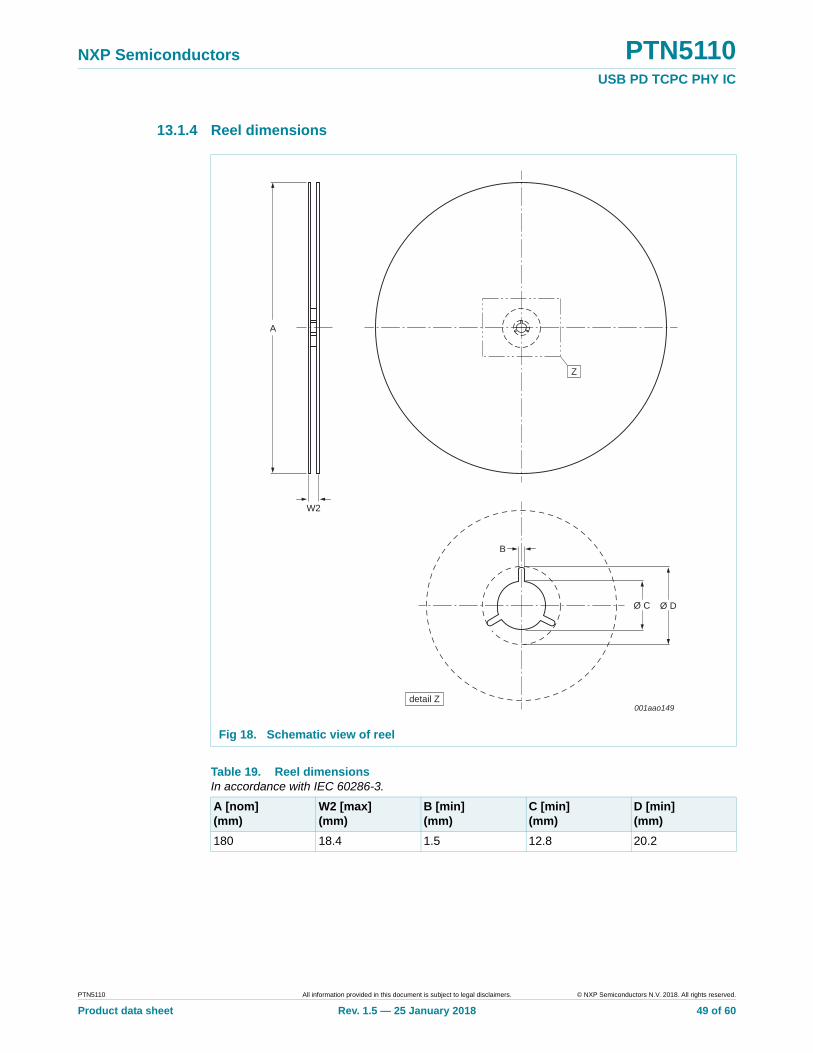
NXP Semiconductors PTN5110USB PD TCPC PHY IC
13.1.4 Reel dimensions
Fig 18. Schematic view of reel
Table 19. Reel dimensionsIn accordance with IEC 60286-3.
A [nom](mm)
W2 [max](mm)
B [min](mm)
C [min](mm)
D [min](mm)
180 18.4 1.5 12.8 20.2
detail Z
B
001aao149
W2
Ø C Ø D
A
Z
PTN5110 All information provided in this document is subject to legal disclaimers. © NXP Semiconductors N.V. 2018. All rights reserved.
Product data sheet Rev. 1.5 — 25 January 2018 49 of 60
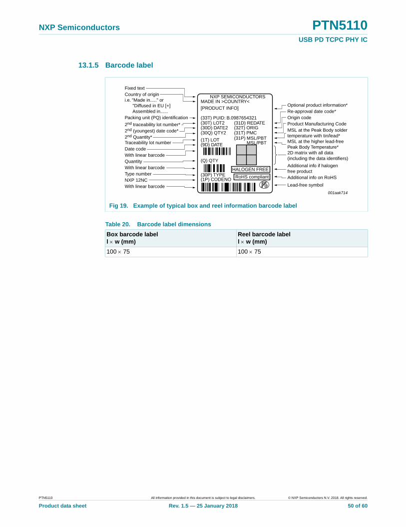
NXP Semiconductors PTN5110USB PD TCPC PHY IC
13.1.5 Barcode label
Fig 19. Example of typical box and reel information barcode label
Table 20. Barcode label dimensions
Box barcode labell w (mm)
Reel barcode labell w (mm)
100 75 100 75
001aak714
NXP SEMICONDUCTORSMADE IN >COUNTRY<[PRODUCT INFO]
(33T) PUID: B.0987654321(30T) LOT2(30D) DATE2(30Q) QTY2
(31D) REDATE(32T) ORIG(31T) PMC(31P) MSL/PBT
MSL/PBT
Optional product information*
Fixed textCountry of origini.e. "Made in....." or "Diffused in EU [+] Assembled in......Packing unit (PQ) identification
2nd traceability lot number*
Traceability lot numberDate codeWith linear barcode
With linear barcode
With linear barcode
Type numberNXP 12NC
Quantity
2nd (youngest) date code*2nd Quantity*
Re-approval date code*Origin codeProduct Manufacturing CodeMSL at the Peak Body soldertemperature with tin/lead*MSL at the higher lead-freePeak Body Temperature*2D matrix with all data(including the data identifiers)
Additional info if halogenfree productAdditional info on RoHS
Lead-free symbol
HALOGEN FREE
RoHS compliant
(1T) LOT(9D) DATE
(Q) QTY
(30P) TYPE(1P) CODENO
PTN5110 All information provided in this document is subject to legal disclaimers. © NXP Semiconductors N.V. 2018. All rights reserved.
Product data sheet Rev. 1.5 — 25 January 2018 50 of 60
NXP Semiconductors PTN5110USB PD TCPC PHY IC
14. Soldering of SMD packages
This text provides a very brief insight into a complex technology. A more in-depth account of soldering ICs can be found in Application Note AN10365 “Surface mount reflow soldering description”.
14.1 Introduction to soldering
Soldering is one of the most common methods through which packages are attached to Printed Circuit Boards (PCBs), to form electrical circuits. The soldered joint provides both the mechanical and the electrical connection. There is no single soldering method that is ideal for all IC packages. Wave soldering is often preferred when through-hole and Surface Mount Devices (SMDs) are mixed on one printed wiring board; however, it is not suitable for fine pitch SMDs. Reflow soldering is ideal for the small pitches and high densities that come with increased miniaturization.
14.2 Wave and reflow soldering
Wave soldering is a joining technology in which the joints are made by solder coming from a standing wave of liquid solder. The wave soldering process is suitable for the following:
• Through-hole components
• Leaded or leadless SMDs, which are glued to the surface of the printed circuit board
Not all SMDs can be wave soldered. Packages with solder balls, and some leadless packages which have solder lands underneath the body, cannot be wave soldered. Also, leaded SMDs with leads having a pitch smaller than ~0.6 mm cannot be wave soldered, due to an increased probability of bridging.
The reflow soldering process involves applying solder paste to a board, followed by component placement and exposure to a temperature profile. Leaded packages, packages with solder balls, and leadless packages are all reflow solderable.
Key characteristics in both wave and reflow soldering are:
• Board specifications, including the board finish, solder masks and vias
• Package footprints, including solder thieves and orientation
• The moisture sensitivity level of the packages
• Package placement
• Inspection and repair
• Lead-free soldering versus SnPb soldering
14.3 Wave soldering
Key characteristics in wave soldering are:
• Process issues, such as application of adhesive and flux, clinching of leads, board transport, the solder wave parameters, and the time during which components are exposed to the wave
• Solder bath specifications, including temperature and impurities
PTN5110 All information provided in this document is subject to legal disclaimers. © NXP Semiconductors N.V. 2018. All rights reserved.
Product data sheet Rev. 1.5 — 25 January 2018 51 of 60
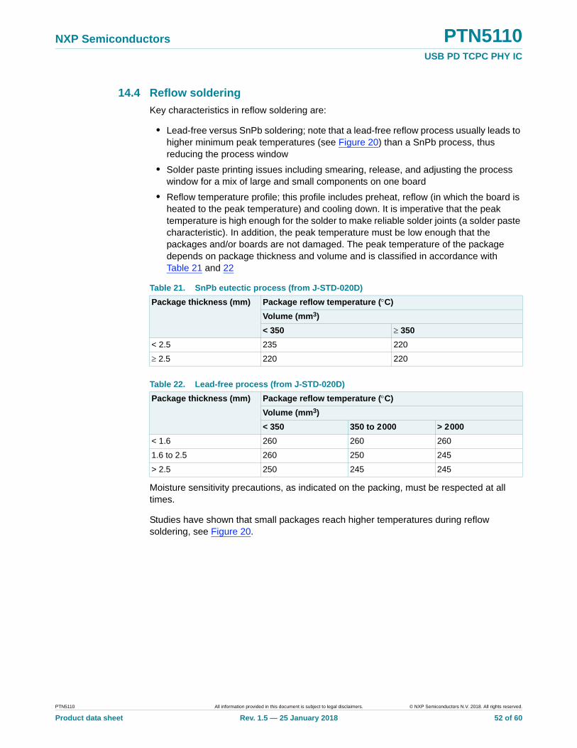
NXP Semiconductors PTN5110USB PD TCPC PHY IC
14.4 Reflow soldering
Key characteristics in reflow soldering are:
• Lead-free versus SnPb soldering; note that a lead-free reflow process usually leads to higher minimum peak temperatures (see Figure 20) than a SnPb process, thus reducing the process window
• Solder paste printing issues including smearing, release, and adjusting the process window for a mix of large and small components on one board
• Reflow temperature profile; this profile includes preheat, reflow (in which the board is heated to the peak temperature) and cooling down. It is imperative that the peak temperature is high enough for the solder to make reliable solder joints (a solder paste characteristic). In addition, the peak temperature must be low enough that the packages and/or boards are not damaged. The peak temperature of the package depends on package thickness and volume and is classified in accordance with Table 21 and 22
Moisture sensitivity precautions, as indicated on the packing, must be respected at all times.
Studies have shown that small packages reach higher temperatures during reflow soldering, see Figure 20.
Table 21. SnPb eutectic process (from J-STD-020D)
Package thickness (mm) Package reflow temperature (C)
Volume (mm3)
< 350 350
< 2.5 235 220
2.5 220 220
Table 22. Lead-free process (from J-STD-020D)
Package thickness (mm) Package reflow temperature (C)
Volume (mm3)
< 350 350 to 2000 > 2000
< 1.6 260 260 260
1.6 to 2.5 260 250 245
> 2.5 250 245 245
PTN5110 All information provided in this document is subject to legal disclaimers. © NXP Semiconductors N.V. 2018. All rights reserved.
Product data sheet Rev. 1.5 — 25 January 2018 52 of 60
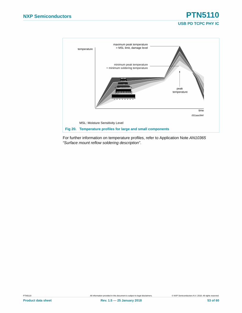
NXP Semiconductors PTN5110USB PD TCPC PHY IC
For further information on temperature profiles, refer to Application Note AN10365 “Surface mount reflow soldering description”.
MSL: Moisture Sensitivity Level
Fig 20. Temperature profiles for large and small components
001aac844
temperature
time
minimum peak temperature= minimum soldering temperature
maximum peak temperature= MSL limit, damage level
peak temperature
PTN5110 All information provided in this document is subject to legal disclaimers. © NXP Semiconductors N.V. 2018. All rights reserved.
Product data sheet Rev. 1.5 — 25 January 2018 53 of 60
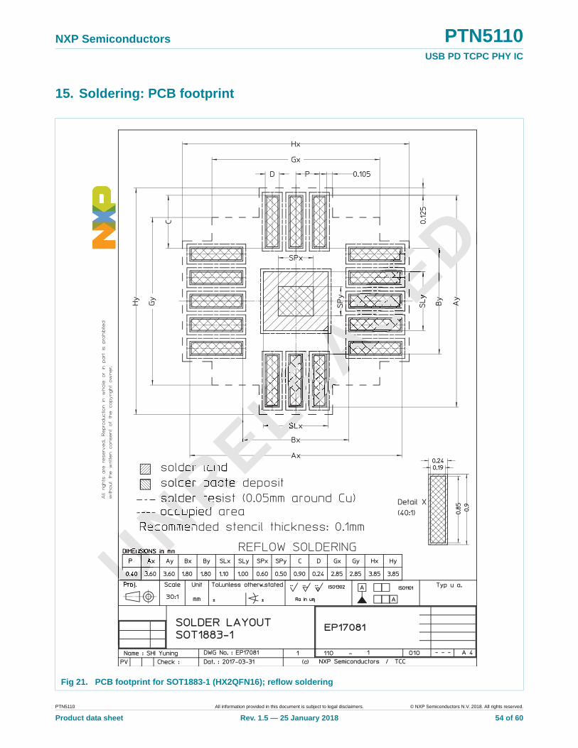
NXP Semiconductors PTN5110USB PD TCPC PHY IC
15. Soldering: PCB footprint
Fig 21. PCB footprint for SOT1883-1 (HX2QFN16); reflow soldering
UNRENNNNNUNUNUNUNUNNNNNNNNNNRNRNRNRRRRRRRNNNRNRNRNRRRRRRNNNRNRNRNRNRNRRRRRRRERERE
UUUUUUUUNRELEASED
LLELLELLELELELELELEELELELELLLELELELELELELEELEEEEEELELELELELEEEEEELELELELELEEEEEEEAEEAEAEAEAEAEAEAEEEEAEAEAEAEAEAEAEAEEESSSASASASASASASSSASASASASASSSSASASASASSSESSE
ASSEASSEASSASSSSSSESESESSSSESESESESSSSSESESEESESESESESESSESESESSEEEEEEAA
LLELLLELELELLLLLLEELELELELEEEELELELEEAEAEAEAEAEAEAEAEAEEEEEAASASASASASASASASASASSSASSASESEASESEASSSSESEASSESEESEESSSESESESEEEEESESESESESSSS
LELELELELEEEEEEESESES
LEL
EEE
LLLEAEAEAAAAAEEELELELELELELELELEEEELELELELEEEEEEAEAEAELLLLLL
EEESESESESSASASASASASSSAAAAELEAAAAAAEEEAEAEAEEAAAAEASAAAAAAAAAAAAAASSASASASAAAAAAAAAAASAS
EAEAAASASASASASAAAASEDEEDDASESESEEESESESSESESESSSSSSASASASASASASASASASAS
ELEAELELELLLEL
AEELEL
EASEEEE
ELRERR
AAAAED
EAEDEDEDD
UUUUUUUNUUUUUUUUUUUUUUUUUUUUUUNUNUNUNUNUNUNUNUNNN
PTN5110 All information provided in this document is subject to legal disclaimers. © NXP Semiconductors N.V. 2018. All rights reserved.
Product data sheet Rev. 1.5 — 25 January 2018 54 of 60

NXP Semiconductors PTN5110USB PD TCPC PHY IC
16. Abbreviations
Table 23. Abbreviations
Acronym Description
AP Application Processor
ASIC Application Specific Integrated Circuit
CDM Charged Device Model, an ESD standard
CPU Central Processing Unit
CL Current Limiting
DBP Dead Battery Provisioning
DFP Downstream Facing Port
DRP Dual Role Port
EC Embedded Controller
FCP Forward Current Protection
FS USB Full Speed signaling
FRS Fast Role Swap
HBM Human Body Model, an ESD standard
HS USB High Speed signaling
LDO Low Drop-Out regulator
LS USB Low Speed signaling
MM Machine Model, an ESD standard
OC Over-Current condition
OCL Over-Current Limiting, a form of Over-Current Protection
OTP Over Temperature Protection
OVP Over Voltage Protection
PCH Platform Controller Hub
PD Power Delivery specification
PMIC Power Management IC
POR Power ON Reset
RCP Reverse Current Protection
RVP Reverse Voltage Protection
SMC System Management Controller
SS USB3.0 Super Speed Signaling
TCPC Type-C Port Controller
TCPCI Type-C Port Controller Interface
TCPM Type-C Port Manager
UFP Upstream Facing Port
USB Universal Serial Bus
PTN5110 All information provided in this document is subject to legal disclaimers. © NXP Semiconductors N.V. 2018. All rights reserved.
Product data sheet Rev. 1.5 — 25 January 2018 55 of 60
NXP Semiconductors PTN5110USB PD TCPC PHY IC
17. References
[1] USB Power Delivery Specification Revision 3.0, Version 1.1 January 12, 2017 (http://www.usb.org/developers/docs/)
[2] USB Type-C Cable and Connector Specification Revision 1.2, March 25, 2016 (http://www.usb.org/developers/docs/)
[3] USB Type-C Port Controller Interface Specification, Rev 2.0, Version 1.0, October 2017 (http://www.usb.org/developers/docs/)
[4] UM10204, “I2C-bus specification and user manual”; NXP Semiconductors, Revision 06 April 4, 2014
[5] PTN5110 Application Programming guide; contact NXP for more information
PTN5110 All information provided in this document is subject to legal disclaimers. © NXP Semiconductors N.V. 2018. All rights reserved.
Product data sheet Rev. 1.5 — 25 January 2018 56 of 60
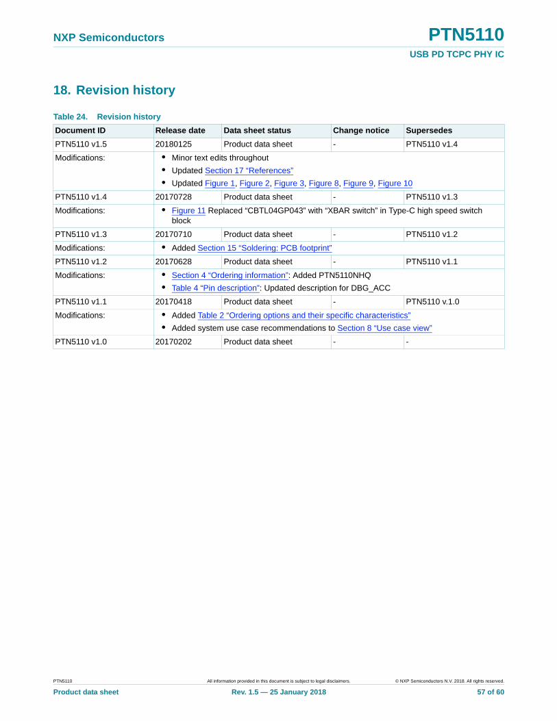
NXP Semiconductors PTN5110USB PD TCPC PHY IC
18. Revision history
Table 24. Revision history
Document ID Release date Data sheet status Change notice Supersedes
PTN5110 v1.5 20180125 Product data sheet - PTN5110 v1.4
Modifications: • Minor text edits throughout
• Updated Section 17 “References”
• Updated Figure 1, Figure 2, Figure 3, Figure 8, Figure 9, Figure 10
PTN5110 v1.4 20170728 Product data sheet - PTN5110 v1.3
Modifications: • Figure 11 Replaced “CBTL04GP043” with “XBAR switch” in Type-C high speed switch block
PTN5110 v1.3 20170710 Product data sheet - PTN5110 v1.2
Modifications: • Added Section 15 “Soldering: PCB footprint”
PTN5110 v1.2 20170628 Product data sheet - PTN5110 v1.1
Modifications: • Section 4 “Ordering information”: Added PTN5110NHQ
• Table 4 “Pin description”: Updated description for DBG_ACC
PTN5110 v1.1 20170418 Product data sheet - PTN5110 v.1.0
Modifications: • Added Table 2 “Ordering options and their specific characteristics”
• Added system use case recommendations to Section 8 “Use case view”
PTN5110 v1.0 20170202 Product data sheet - -
PTN5110 All information provided in this document is subject to legal disclaimers. © NXP Semiconductors N.V. 2018. All rights reserved.
Product data sheet Rev. 1.5 — 25 January 2018 57 of 60

NXP Semiconductors PTN5110USB PD TCPC PHY IC
19. Legal information
19.1 Data sheet status
[1] Please consult the most recently issued document before initiating or completing a design.
[2] The term ‘short data sheet’ is explained in section “Definitions”.
[3] The product status of device(s) described in this document may have changed since this document was published and may differ in case of multiple devices. The latest product status information is available on the Internet at URL http://www.nxp.com.
19.2 Definitions
Draft — The document is a draft version only. The content is still under internal review and subject to formal approval, which may result in modifications or additions. NXP Semiconductors does not give any representations or warranties as to the accuracy or completeness of information included herein and shall have no liability for the consequences of use of such information.
Short data sheet — A short data sheet is an extract from a full data sheet with the same product type number(s) and title. A short data sheet is intended for quick reference only and should not be relied upon to contain detailed and full information. For detailed and full information see the relevant full data sheet, which is available on request via the local NXP Semiconductors sales office. In case of any inconsistency or conflict with the short data sheet, the full data sheet shall prevail.
Product specification — The information and data provided in a Product data sheet shall define the specification of the product as agreed between NXP Semiconductors and its customer, unless NXP Semiconductors and customer have explicitly agreed otherwise in writing. In no event however, shall an agreement be valid in which the NXP Semiconductors product is deemed to offer functions and qualities beyond those described in the Product data sheet.
19.3 Disclaimers
Limited warranty and liability — Information in this document is believed to be accurate and reliable. However, NXP Semiconductors does not give any representations or warranties, expressed or implied, as to the accuracy or completeness of such information and shall have no liability for the consequences of use of such information. NXP Semiconductors takes no responsibility for the content in this document if provided by an information source outside of NXP Semiconductors.
In no event shall NXP Semiconductors be liable for any indirect, incidental, punitive, special or consequential damages (including - without limitation - lost profits, lost savings, business interruption, costs related to the removal or replacement of any products or rework charges) whether or not such damages are based on tort (including negligence), warranty, breach of contract or any other legal theory.
Notwithstanding any damages that customer might incur for any reason whatsoever, NXP Semiconductors’ aggregate and cumulative liability towards customer for the products described herein shall be limited in accordance with the Terms and conditions of commercial sale of NXP Semiconductors.
Right to make changes — NXP Semiconductors reserves the right to make changes to information published in this document, including without limitation specifications and product descriptions, at any time and without notice. This document supersedes and replaces all information supplied prior to the publication hereof.
Suitability for use — NXP Semiconductors products are not designed, authorized or warranted to be suitable for use in life support, life-critical or safety-critical systems or equipment, nor in applications where failure or malfunction of an NXP Semiconductors product can reasonably be expected to result in personal injury, death or severe property or environmental damage. NXP Semiconductors and its suppliers accept no liability for inclusion and/or use of NXP Semiconductors products in such equipment or applications and therefore such inclusion and/or use is at the customer’s own risk.
Applications — Applications that are described herein for any of these products are for illustrative purposes only. NXP Semiconductors makes no representation or warranty that such applications will be suitable for the specified use without further testing or modification.
Customers are responsible for the design and operation of their applications and products using NXP Semiconductors products, and NXP Semiconductors accepts no liability for any assistance with applications or customer product design. It is customer’s sole responsibility to determine whether the NXP Semiconductors product is suitable and fit for the customer’s applications and products planned, as well as for the planned application and use of customer’s third party customer(s). Customers should provide appropriate design and operating safeguards to minimize the risks associated with their applications and products.
NXP Semiconductors does not accept any liability related to any default, damage, costs or problem which is based on any weakness or default in the customer’s applications or products, or the application or use by customer’s third party customer(s). Customer is responsible for doing all necessary testing for the customer’s applications and products using NXP Semiconductors products in order to avoid a default of the applications and the products or of the application or use by customer’s third party customer(s). NXP does not accept any liability in this respect.
Limiting values — Stress above one or more limiting values (as defined in the Absolute Maximum Ratings System of IEC 60134) will cause permanent damage to the device. Limiting values are stress ratings only and (proper) operation of the device at these or any other conditions above those given in the Recommended operating conditions section (if present) or the Characteristics sections of this document is not warranted. Constant or repeated exposure to limiting values will permanently and irreversibly affect the quality and reliability of the device.
Terms and conditions of commercial sale — NXP Semiconductors products are sold subject to the general terms and conditions of commercial sale, as published at http://www.nxp.com/profile/terms, unless otherwise agreed in a valid written individual agreement. In case an individual agreement is concluded only the terms and conditions of the respective agreement shall apply. NXP Semiconductors hereby expressly objects to applying the customer’s general terms and conditions with regard to the purchase of NXP Semiconductors products by customer.
No offer to sell or license — Nothing in this document may be interpreted or construed as an offer to sell products that is open for acceptance or the grant, conveyance or implication of any license under any copyrights, patents or other industrial or intellectual property rights.
Document status[1][2] Product status[3] Definition
Objective [short] data sheet Development This document contains data from the objective specification for product development.
Preliminary [short] data sheet Qualification This document contains data from the preliminary specification.
Product [short] data sheet Production This document contains the product specification.
PTN5110 All information provided in this document is subject to legal disclaimers. © NXP Semiconductors N.V. 2018. All rights reserved.
Product data sheet Rev. 1.5 — 25 January 2018 58 of 60
NXP Semiconductors PTN5110USB PD TCPC PHY IC
Export control — This document as well as the item(s) described herein may be subject to export control regulations. Export might require a prior authorization from competent authorities.
Quick reference data — The Quick reference data is an extract of the product data given in the Limiting values and Characteristics sections of this document, and as such is not complete, exhaustive or legally binding.
Non-automotive qualified products — Unless this data sheet expressly states that this specific NXP Semiconductors product is automotive qualified, the product is not suitable for automotive use. It is neither qualified nor tested in accordance with automotive testing or application requirements. NXP Semiconductors accepts no liability for inclusion and/or use of non-automotive qualified products in automotive equipment or applications.
In the event that customer uses the product for design-in and use in automotive applications to automotive specifications and standards, customer (a) shall use the product without NXP Semiconductors’ warranty of the
product for such automotive applications, use and specifications, and (b) whenever customer uses the product for automotive applications beyond NXP Semiconductors’ specifications such use shall be solely at customer’s own risk, and (c) customer fully indemnifies NXP Semiconductors for any liability, damages or failed product claims resulting from customer design and use of the product for automotive applications beyond NXP Semiconductors’ standard warranty and NXP Semiconductors’ product specifications.
Translations — A non-English (translated) version of a document is for reference only. The English version shall prevail in case of any discrepancy between the translated and English versions.
19.4 TrademarksNotice: All referenced brands, product names, service names and trademarks are the property of their respective owners.
20. Contact information
For more information, please visit: http://www.nxp.com
For sales office addresses, please send an email to: [email protected]
PTN5110 All information provided in this document is subject to legal disclaimers. © NXP Semiconductors N.V. 2018. All rights reserved.
Product data sheet Rev. 1.5 — 25 January 2018 59 of 60
NXP Semiconductors PTN5110USB PD TCPC PHY IC
21. Contents
1 General description . . . . . . . . . . . . . . . . . . . . . . 1
2 Features and benefits . . . . . . . . . . . . . . . . . . . . 22.1 USB PD and Type-C features. . . . . . . . . . . . . . 22.2 System protection features. . . . . . . . . . . . . . . . 32.3 General . . . . . . . . . . . . . . . . . . . . . . . . . . . . . . . 3
3 Applications . . . . . . . . . . . . . . . . . . . . . . . . . . . . 4
4 Ordering information. . . . . . . . . . . . . . . . . . . . . 54.1 Ordering options . . . . . . . . . . . . . . . . . . . . . . . . 5
5 Block diagram . . . . . . . . . . . . . . . . . . . . . . . . . . 7
6 Pinning information. . . . . . . . . . . . . . . . . . . . . . 86.1 Pinning . . . . . . . . . . . . . . . . . . . . . . . . . . . . . . . 86.2 Pin description . . . . . . . . . . . . . . . . . . . . . . . . . 8
7 Functional description . . . . . . . . . . . . . . . . . . 107.1 Type-C Configuration Channel functional block . .
107.2 USB power delivery function . . . . . . . . . . . . . 117.3 VCONN switch and control . . . . . . . . . . . . . . . 127.3.1 Reverse Voltage Protection (RVP) . . . . . . . . . 127.3.2 Over Current Limiting (OCL). . . . . . . . . . . . . . 127.3.3 Over Temperature Protection (OTP). . . . . . . . 137.3.4 Short to GND protection . . . . . . . . . . . . . . . . . 137.4 VBUS power path control . . . . . . . . . . . . . . . . 137.5 Host interface and control. . . . . . . . . . . . . . . . 157.6 Power management and power supplies . . . . 17
8 Use case view . . . . . . . . . . . . . . . . . . . . . . . . . 188.1 System use case . . . . . . . . . . . . . . . . . . . . . . 198.1.1 USB PD DRP (Provider/Consumer): Notebook PC
with buck boost charger . . . . . . . . . . . . . . . . . 198.1.2 USB PD DRP (Provider/Consumer): Notebook PC
with regular NVDC charger . . . . . . . . . . . . . . 218.1.3 USB PD Source (Provider) with Type-C
receptacle: Desktop PC . . . . . . . . . . . . . . . . . 248.1.4 USB PD DRP (Provider/Consumer: Smartphone
use case) Standalone PTN5110 . . . . . . . . . . 268.1.5 Type-C adapters with PTN5110 . . . . . . . . . . . 288.1.6 USB PD with DRP w/Try.SRC and Type-C
receptacle . . . . . . . . . . . . . . . . . . . . . . . . . . . . 298.1.7 USB PD Sink (Consumer) with Type-C receptacle
308.1.8 Multi-port PD PHY use case. . . . . . . . . . . . . . 31
9 Limiting values. . . . . . . . . . . . . . . . . . . . . . . . . 33
10 Recommended operating conditions. . . . . . . 34
11 Characteristics. . . . . . . . . . . . . . . . . . . . . . . . . 3511.1 Device characteristics. . . . . . . . . . . . . . . . . . . 3511.2 USB PD and Type-C characteristics. . . . . . . . 37
11.3 USB VBUS and VCONN timing AC/DC characteristics . . . . . . . . . . . . . . . . . . . . . . . . 40
11.4 VCONN switch characteristics . . . . . . . . . . . . 4111.5 I2C characteristics . . . . . . . . . . . . . . . . . . . . . 4211.6 Control I/O characteristics . . . . . . . . . . . . . . . 44
12 Package outline. . . . . . . . . . . . . . . . . . . . . . . . 46
13 Packing information . . . . . . . . . . . . . . . . . . . . 4713.1 HX2QFN16; Reel pack, SMD, 7"; Q2/T3 standard
product orientation; Orderable part number ending ,147 or Z; Ordering code (12NC) ending 147 47
13.1.1 Packing method . . . . . . . . . . . . . . . . . . . . . . . 4713.1.2 Product orientation. . . . . . . . . . . . . . . . . . . . . 4813.1.3 Carrier tape dimensions. . . . . . . . . . . . . . . . . 4813.1.4 Reel dimensions . . . . . . . . . . . . . . . . . . . . . . 4913.1.5 Barcode label . . . . . . . . . . . . . . . . . . . . . . . . . 50
14 Soldering of SMD packages. . . . . . . . . . . . . . 5114.1 Introduction to soldering. . . . . . . . . . . . . . . . . 5114.2 Wave and reflow soldering. . . . . . . . . . . . . . . 5114.3 Wave soldering . . . . . . . . . . . . . . . . . . . . . . . 5114.4 Reflow soldering . . . . . . . . . . . . . . . . . . . . . . 52
15 Soldering: PCB footprint . . . . . . . . . . . . . . . . 54
16 Abbreviations . . . . . . . . . . . . . . . . . . . . . . . . . 55
17 References. . . . . . . . . . . . . . . . . . . . . . . . . . . . 56
18 Revision history . . . . . . . . . . . . . . . . . . . . . . . 57
19 Legal information . . . . . . . . . . . . . . . . . . . . . . 5819.1 Data sheet status . . . . . . . . . . . . . . . . . . . . . . 5819.2 Definitions . . . . . . . . . . . . . . . . . . . . . . . . . . . 5819.3 Disclaimers . . . . . . . . . . . . . . . . . . . . . . . . . . 5819.4 Trademarks . . . . . . . . . . . . . . . . . . . . . . . . . . 59
20 Contact information . . . . . . . . . . . . . . . . . . . . 59
21 Contents. . . . . . . . . . . . . . . . . . . . . . . . . . . . . . 60
© NXP Semiconductors N.V. 2018. All rights reserved.
For more information, please visit: http://www.nxp.comFor sales office addresses, please send an email to: [email protected]
Date of release: 25 January 2018
Document identifier: PTN5110
Please be aware that important notices concerning this document and the product(s)described herein, have been included in section ‘Legal information’.