1. general description of the msb-justified output format and the lsb-justified input format. the...
TRANSCRIPT

1. General description
The UDA1338H is a single-chip consisting of 4 plus 1 analog-to-digital converters and 6 digital-to-analog converters with signal processing features employing bitstream conversion techniques. The multichannel configuration makes the device eminently suitable for use in digital audio equipment which incorporates surround feature.
The UDA1338H supports conventional 2 channels per line data transfer conformable to the I2S-bus format with word lengths of up to 24 bits, the MSB-justified format with word lengths of up to 24 bits and the LSB-justified format with word lengths of 16 bits, 20 bits and 24 bits, as well as 4 to 6 channels per line transfer mode. The device also supports a combination of the MSB-justified output format and the LSB-justified input format. The UDA1338H has special sound processing features in the Direct Stream Digital (DSD) playback mode, de-emphasis, volume and mute which can be controlled via the L3-bus or I2C-bus interface.
2. Features and benefits
2.1 General2.7 V to 3.6 V power supply5 V tolerant digital inputs24-bit data pathSelectable control: via L3-bus or I2C-bus microcontroller interfaceSupports sample frequency ranges for:
Audio ADC: fs = 16 kHz to 100 kHzVoice ADC: fs = 7 kHz to 50 kHzAudio DAC: fs = 16 kHz to 200 kHz
Separate power control for ADC and DACADC plus integrated high-pass filter to cancel DC offsetIntegrated digital filter plus DACSlave mode only applicationsEasy application
UDA1338HMultichannel audio coder-decoderRev. 04 — 18 May 2010 Product data sheet

NXP Semiconductors UDA1338HMultichannel audio coder-decoder
2.2 Multiple format data interfaceAudio interface supports standard I2S-bus, MSB-justified, LSB-justified and two multichannel formatsVoice interface supports I2S-bus and mono channel formats
2.3 Digital sound processingControl via L3-bus or I2C-bus:
Channel independent digital logarithmic volumeDigital de-emphasis for fs = 32 kHz, 44.1 kHz, 48 kHz or 96 kHzSoft or quick muteOutput signal polarity control
2.4 Advanced audio configurationInputs:
4 single-ended audio inputs (2 × stereo) with programmable gain amplifiers1 single-ended voice input
Outputs:6 differential audio outputs (3 × stereo)
DSD mode to support stereo DSD playbackHigh linearity, wide dynamic range and low distortionDAC digital filter with selectable sharp or soft roll-off
3. Applications
Excellently suitable for multichannel home audio-video application
4. Quick reference data
Table 1: Quick reference dataVDDD = VDDA(AD) = VDDA(DA) = 3.3 V; Tamb = 25 °C; RL = 22 kΩ; all voltages referenced to ground (pins VSS); unless otherwise specified.
Symbol Parameter Conditions Min. Typ. Max. UnitSuppliesVDDA(AD) ADC analog supply
voltage2.7 3.3 3.6 V
VDDA(DA) DAC analog supply voltage
2.7 3.3 3.6 V
VDDD digital supply voltage 2.7 3.3 3.6 V
IDDA(AD) ADC analog supply current
fADC = 48 kHz - 30 - mA
IDDA(DA) DAC analog supply current
fDAC = 48 kHz - 20 - mA
IDDD digital supply current fADC = fDAC = 48 kHz; fVOICE = 48 kHz
- 31 - mA
UDA1338H All information provided in this document is subject to legal disclaimers. © NXP B.V. 2010. All rights reserved.
Product data sheet Rev. 04 — 18 May 2010 2 of 55
NXP Semiconductors UDA1338HMultichannel audio coder-decoder
[1] The input voltage can be up to 2 V (RMS) when the current through the ADC input pin is limited to approximately 1 mA by using a series resistor.
[2] The input voltage to the ADC scales proportionally with the power supply voltage.
5. Ordering information
IDDD(pd) digital supply current in Power-down mode
audio and voice ADCs power-down
- 18 - mA
DAC power-down - 14 - mA
Tamb ambient temperature −20 - +85 °C
Audio analog-to-digital converterD0 digital output level at 0 dB setting;
900 mV (RMS) input[1][2] −2.5 −1.2 −0.7 dB
(THD+N)/S total harmonic distortion-plus-noise to signal ratio
at −1 dBFS - −90 −83 dB
at −60 dBFS; A-weighted
- −40 −34 dB
S/N signal-to-noise ratio code = 0; A-weighted 94 100 - dB
αcs channel separation - 100 - dB
Digital-to-analog converterDifferential mode
Vo(rms) output voltage (RMS value)
at 0 dBFS digital input 1.9 2.0 2.1 V
(THD+N)/S total harmonic distortion-plus-noise to signal ratio
at 0 dBFS - −100 −93 dB
at −60 dBFS; A-weighted
- −50 −45 dB
S/N signal-to-noise ratio code = 0; A-weighted 107 114 - dB
αcs channel separation - 117 - dB
Single-ended mode
Vo(rms) output voltage (RMS value)
at 0 dBFS digital input - 1.0 - V
(THD+N)/S total harmonic distortion-plus-noise to signal ratio
at 0 dBFS - −90 - dB
at −60 dBFS; A-weighted
- −45 - dB
S/N signal-to-noise ratio code = 0; A-weighted - 110 - dB
αcs channel separation - 114 - dB
Table 1: Quick reference data …continuedVDDD = VDDA(AD) = VDDA(DA) = 3.3 V; Tamb = 25 °C; RL = 22 kΩ; all voltages referenced to ground (pins VSS); unless otherwise specified.
Symbol Parameter Conditions Min. Typ. Max. Unit
Table 2: Ordering informationType number
PackageName Description Version
UDA1338H QFP44 plastic quad flat package; 44 leads (lead length 1.3 mm); body 10 × 10 × 1.75 mm
SOT307-2
UDA1338H All information provided in this document is subject to legal disclaimers. © NXP B.V. 2010. All rights reserved.
Product data sheet Rev. 04 — 18 May 2010 3 of 55

NXP Semiconductors UDA1338HMultichannel audio coder-decoder
6. Block diagram
Fig 1. Block diagram
mgu581
PGA ADC 2L
PLL
PLL
I2S-BUSINTERFACE 3
HP FILTER
DECIMATIONFILTER
6
21
20
22
30
37 40
24
23
VINL2
MCCLK
MCMODE
MCDATA
I2C_L3
BCKDA
WSDA
5 3
DECIMATION FILTER
DC-CANCELLATION FILTER
I2S-BUSINTERFACE 2
L3-BUS ORI2C-BUS
CONTROLINTERFACE
VDDA(DA) VSSA(DA)
INTERPOLATION FILTER
VOLUME, MUTE, DE-EMPHASIS
NOISE SHAPER
I2S-BUSINTERFACE 1
VDDA(AD)
9
VADCP
7
VADCN
1
VrefVSSA(AD)
UDA1338H
LNA10
VVOICE
PGA ADC 1L
PGAADC 2R
PGAADC 1R2
VINL1
VOUT2N
VOUT2P
VOUT4N
VOUT4P
VOUT6N
VOUT6P
VOUT1N
VOUT1P
VOUT3N
VOUT3P
VOUT5N
VOUT5P
DAC 2
34−
+ 33
39
38
44
43
32
31
36
35
42
41
DAC 4−
+
DAC 6
DAC 1
DAC 3
DAC 5−
+
−
+
ADC
CLOCK
TEST
−
+
−
+
25DATADA1
26DATADA2
27DATADA3
13DATAAD1
12DATAAD2
14BCKAD
11TEST
4VINR1
8VINR2
19SYSCLK
15WSAD17
BCKV
16DATAV
18WSV
28
29VDDD
VSSD
UDA1338H All information provided in this document is subject to legal disclaimers. © NXP B.V. 2010. All rights reserved.
Product data sheet Rev. 04 — 18 May 2010 4 of 55

NXP Semiconductors UDA1338HMultichannel audio coder-decoder
7. Pinning information
7.1 Pinning
7.2 Pin description
Fig 2. Pin configuration
UDA1338H
Vref VOUT2P
VINL1 VOUT1N
VSSA(AD) VOUT1P
VINR1 I2C_L3
VDDA(AD) VDDD
VINL2 VSSD
VADCN DATADA3
VINR2 DATADA2
VADCP DATADA1
VVOICE BCKDA
TEST WSDA
DA
TA
AD
2V
OU
T6N
DA
TA
AD
1V
OU
T6P
BC
KA
DV
OU
T5N
WS
AD
VO
UT
5P
DA
TA
VV
SS
A(D
A)
BC
KV
VO
UT
4N
WS
VV
OU
T4P
SY
SC
LKV
DD
A(D
A)
MC
MO
DE
VO
UT
3N
MC
CLK
VO
UT
3P
MC
DA
TA
VO
UT
2N
001aac293
1
2
3
4
5
6
7
8
9
10
11
33
32
31
30
29
28
27
26
25
24
23
12 13 14 15 16 17 18 19 20 21 22
44 43 42 41 40 39 38 37 36 35 34
Table 3: Pin descriptionSymbol Pin Type[1] DescriptionVref 1 AIO ADC reference voltage
VINL1 2 AIO ADC 1 input left
VSSA(AD) 3 AGND ADC analog ground
VINR1 4 AIO ADC 1 input right
VDDA(AD) 5 AS ADC analog supply voltage
VINL2 6 AIO ADC 2 input left
VADCN 7 AIO ADC reference voltage N
VINR2 8 AIO ADC 2 input right
VADCP 9 AIO ADC reference voltage P
VVOICE 10 AIO voice ADC input
TEST 11 DID test input; must be connected to digital ground (VSSD) in application
DATAAD2 12 DO ADC 2 data output
DATAAD1 13 DO ADC 1 data output
BCKAD 14 DIS ADC bit clock input
WSAD 15 DI ADC word select input
UDA1338H All information provided in this document is subject to legal disclaimers. © NXP B.V. 2010. All rights reserved.
Product data sheet Rev. 04 — 18 May 2010 5 of 55
NXP Semiconductors UDA1338HMultichannel audio coder-decoder
[1] See Table 4.
DATAV 16 DO voice data output
BCKV 17 DIS voice bit clock input
WSV 18 DIO voice word select input or output
SYSCLK 19 DIS system clock input: 256fs, 384fs, 512fs or 768fsMCMODE 20 DI L3-bus L3MODE input or I2C-bus DAC mute control
input
MCCLK 21 DIS L3-bus L3CLOCK input or I2C-bus SCL input
MCDATA 22 IIC L3-bus L3DATA input and output or I2C-bus SDA input and output
WSDA 23 DI DAC word select input
BCKDA 24 DIS DAC bit clock input
DATADA1 25 DI DAC channel 1 and channel 2 data input
DATADA2 26 DI DAC channel 3 and channel 4 data input
DATADA3 27 DI DAC channel 5 and channel 6 data input
VSSD 28 DGND digital ground
VDDD 29 DS digital supply voltage
I2C_L3 30 DI selection input for L3-bus or I2C-bus control
VOUT1P 31 AIO DAC 1 positive output
VOUT1N 32 AIO DAC 1 negative output
VOUT2P 33 AIO DAC 2 positive output
VOUT2N 34 AIO DAC 2 negative output
VOUT3P 35 AIO DAC 3 positive output
VOUT3N 36 AIO DAC 3 negative output
VDDA(DA) 37 AS DAC analog supply voltage
VOUT4P 38 AIO DAC 4 positive output
VOUT4N 39 AIO DAC 4 negative output
VSSA(DA) 40 AGND DAC analog ground
VOUT5P 41 AIO DAC 5 positive output
VOUT5N 42 AIO DAC 5 negative output
VOUT6P 43 AIO DAC 6 positive output
VOUT6N 44 AIO DAC 6 negative output
Table 4: Pin typesType DescriptionAGND analog ground
AIO analog input and output
AS analog supply
DGND digital ground
DI digital input
DID digital input with internal pull-down resistor
DIO digital input and output
Table 3: Pin description …continued
Symbol Pin Type[1] Description
UDA1338H All information provided in this document is subject to legal disclaimers. © NXP B.V. 2010. All rights reserved.
Product data sheet Rev. 04 — 18 May 2010 6 of 55

NXP Semiconductors UDA1338HMultichannel audio coder-decoder
8. Functional description
8.1 System clockThe UDA1338H operates in slave mode only; this means that in all applications the system must provide either the system clock (the bit clock for the voice ADC) or the word clock.
The audio ADC part, the voice ADC part and the DAC part can operate at different sampling frequencies (DAC-WS and ADC-WS modes) as well as a common frequency (SYSCLK, WSDA and DSD modes).
The voice ADC part supports a sampling frequency up to 50 kHz and the audio ADC supports a sampling frequency up to 100 kHz. The DAC sampling frequency range is extended up to 200 kHz with the range above 100 kHz being supported through 192 kHz sampling mode, which halves the oversampling ratio of SYSCLK and internal clocks.
The mode of operation of the audio and voice channels can be set via the L3-bus or I2C-bus microcontroller interface and are summarized in and Table 6.
When applied, the system clock must be locked in frequency to the corresponding digital interface clocks.
The voice ADC part can either receive or generate the WSV signal as shown in Table 6.
DIS digital Schmitt-triggered input
DO digital output
DS digital supply
IIC input and open-drain output for I2C-bus
Table 4: Pin types …continued
Type Description
Table 5: Audio ADC and DAC operating clock modeMode Audio ADC Audio DAC
Clock Frequency Clock FrequencySYSCLK SYSCLK 256fs, 384fs, 512fs
or 768fsSYSCLK 256fs, 384fs, 512fs
or 768fsSYSCLK 128fs, 192fs, 256fs
or 384fs; 192 kHz sampling mode
DAC-WS SYSCLK 256fs, 384fs, 512fs or 768fs
WSDA 1fs
ADC-WS WSAD 1fs SYSCLK 256fs, 384fs, 512fs or 768fs
SYSCLK 128fs, 192fs, 256fs or 384fs; 192 kHz sampling mode
WSDA WSDA 1fs WSDA 1fsDSD SYSCLK 44.1 kHz × 512 SYSCLK 44.1 kHz × 512
UDA1338H All information provided in this document is subject to legal disclaimers. © NXP B.V. 2010. All rights reserved.
Product data sheet Rev. 04 — 18 May 2010 7 of 55

NXP Semiconductors UDA1338HMultichannel audio coder-decoder
8.2 Audio analog-to-digital converter (audio ADC)The audio analog-to-digital front-end of the UDA1338H consists of 4-channel single-ended Adds with programmable gain stage (from 0 dB to 24 dB with 3 dB steps), controlled via the microcontroller interface. Using the PGA feature, it is possible to accept an input signal of 900 mV (RMS) or 1.8 V (RMS) if an external resistor of 10 kΩ is used in series. The schematic of audio ADC front-end is shown in Figure 3.
8.3 Voice analog-to-digital converter (voice ADC) The voice analog-to-digital front-end of the UDA1338H consists of a single-channel single-ended ADC with a fixed gain (26 dB) Low Noise Amplifier (LNA). Together with the digital variable gain amplification stage, the voice ADC provides optimal processing and reproduction of the microphone signal. The supported sampling frequency range is from 7 kHz to 50 kHz. Power-down of the LNA and the ADC can be controlled separately.
8.4 Decimation filter of audio ADC
The decimation from 64fs is performed in two stages. The first stage realizes
characteristics with a decimation factor of 8. The second stage consists of three half-band filters, each decimating by a factor of 2. The filter characteristics are shown in Table 7.
Table 6: Voice ADC operating clock modeMode Voice ADC
Bit clock frequency (BCKV) Word select (WSV)WSV-in input: 32fs, 64fs, 128fs or 256fs input
WSV-out input: 32fs, 64fs, 128fs or 256fs output
Fig 3. Schematic of audio ADC front-end
mgu582
Vref
ADC
VDDA = 3.3 V
VINL,VINR
10 kΩ (0 dB setting)
10 kΩ10 kΩinput signal2 V (RMS)
Table 7: Decimation filter characteristics (audio ADC)Item Condition Value (dB)Pass-band ripple 0 to 0.45fs ±0.01
Pass-band droop 0.45fs −0.2
Stop band >0.55fs −70
Dynamic range 0 to 0.45fs >135
xsinx
----------⎝ ⎠⎛ ⎞ 4
UDA1338H All information provided in this document is subject to legal disclaimers. © NXP B.V. 2010. All rights reserved.
Product data sheet Rev. 04 — 18 May 2010 8 of 55

NXP Semiconductors UDA1338HMultichannel audio coder-decoder
8.5 Decimation filter of voice ADCThe voice ADC decimation filter is realized with the combination of a Finite Impulse Response (FIR) filter and Infinite Impulse Response (IIR) filter for shorter group delay. The filter characteristics are shown in Table 8. During the power-on sequence, the output of the ADC is hard muted for a certain period. This hard-mute time can be chosen between 1024 and 2048 samples.
8.6 Interpolation filter of DACThe digital interpolation filter interpolates from 1fs to 128fs (or to 64fs in the 192 kHz sampling mode) by cascading FIR filters, and has two sets of filter coefficients for sharp and slow roll-off as given in Table 9 and Table 10.
8.7 Noise shaper of DACThe 3rd-order noise shaper operates at either 128fs or 64fs (in the 192 kHz sampling mode), and converts the 24-bit input signal into a 5-bit signal stream. The noise shaper shifts in-band quantization noise to frequencies well above the audio band. This noise shaping technique enables high signal-to-noise ratios to be achieved.
8.8 Digital mixerThe UDA1338H has 6 digital mixers inside the interpolator; see Figure 4. The ADC signals can be mixed with the I2S-bus input signals. The mixing of the ADC signals can be selected by the bits MIX[1:0].
Table 8: Decimation filter characteristics (voice ADC)Item Condition Value (dB)Pass-band ripple 0 to 0.45fs ±0.05
Pass-band droop 0.45fs −0.2
Stop band >0.55fs −65
Dynamic range 0 to 0.45fs >110
Table 9: Interpolation filter characteristics (sharp roll-off)Item Condition Value (dB)Pass-band ripple 0 to 0.45fs ±0.002
Stop band > 0.55fs −75
Dynamic range 0 to 0.45fs > 135
Table 10: Interpolation filter characteristics (slow roll-off) Item Condition Value (dB)Pass-band ripple 0 to 0.22fs ±0.002
Pass-band droop 0.45fs −3.1
Stop band > 0.78fs −94
Dynamic range 0 to 0.22fs > 135
UDA1338H All information provided in this document is subject to legal disclaimers. © NXP B.V. 2010. All rights reserved.
Product data sheet Rev. 04 — 18 May 2010 9 of 55

NXP Semiconductors UDA1338HMultichannel audio coder-decoder
8.9 Audio digital-to-analog convertersThe audio digital-to-analog front-end of the UDA1338H consists of 6-channel differential SDACs: an SDAC is a multi-bit DAC based upon switched resistors. To minimize data dependent modulation effects, a Dynamic Element Matching (DEM) algorithm scrambler circuit and DC current compensation circuit are implemented with the SDAC.
8.10 Power-on resetThe UDA1338H has an internal power-on reset circuit which initializes the device; see Figure 5. All the digital sound processing features and the system controlling features are set to their default values in the L3-bus and the I2C-bus modes.
The reset time (see Figure 6) is determined by an external capacitor which is connected between pin Vref and ground. The reset time should be at least 250 μs for Vref < 1.25 V. When VDDA(AD) is switched off, the device will be reset again for Vref < 0.75 V.
During the reset time, the system clock should be running.
Fig 4. Block diagram of DAC mixer
mgw786
MIX[1:0]
DIS[1:0]
ICS[1:0]
from ADC
MIXERVOLUME
MIXERMUTE
DAC11fs
VOLUMEDE-EMPHASIS MUTE
DAC2same as above
DAC3same as above
DAC4same as above
DAC5same as above
DAC6same as above
INTERPOLATIONFILTER
ch1mixer inputch2
ch3ch4
from I2S-bus
DATADA1
DATADA2
DATADA3
+
UDA1338H All information provided in this document is subject to legal disclaimers. © NXP B.V. 2010. All rights reserved.
Product data sheet Rev. 04 — 18 May 2010 10 of 55

NXP Semiconductors UDA1338HMultichannel audio coder-decoder
8.11 Audio digital interfaceThe following audio formats can be selected via the microcontroller interface:
• I2S-bus format with data word length of up to 24 bits• MSB-justified format with data word length of up to 24 bits• LSB-justified format with data word length of 16 bits, 20 bits or 24 bits• Multichannel formats with data word length of 20 bits or 24 bits. The used data lines
are DATAAD1 and DATADA1 and the sampling frequency must be below 50 kHz
The formats are illustrated in Figure 7 and Figure 8.
Fig 5. Power-on reset circuit
Fig 6. Power-on reset timing
VDDA(AD)
Vref
mgu585
C1 >10 μF
RESETCIRCUIT
9 kΩ
9 kΩ
3.3
VDDD(V)
0t
3.3
VDDA(AD)(V)
0t
Vref(V)
1.651.250.75
trst
0t
mgu586>250 μs
UDA1338H All information provided in this document is subject to legal disclaimers. © NXP B.V. 2010. All rights reserved.
Product data sheet Rev. 04 — 18 May 2010 11 of 55

xxxxxxxxxxxxxxxxxxxxx xxxxxxxxxxxxxxxxxxxxxxxxxx xxxxxxx x x x xxxxxxxxxxxxxxxxxxxxxxxxxxxxxx xxxxxxxxxxxxxxxxxxx xx xx xxxxx xxxxxxxxxxxxxxxxxxxxxxxxxxx xxxxxxxxxxxxxxxxxxx xxxxxx xxxxxxxxxxxxxxxxxxxxxxxxxxxxxxxxxxx xxxxxxxxxxxx x x xxxxxxxxxxxxxxxxxxxxx xxxxxxxxxxxxxxxxxxxxxxxxxxxxxx xxxxx xxxxxxxxxxxxxxxxxxxxxxxxxxxxxxxxxxxxxxxxxxxxxxxxxx xxxxxxxx xxxxxxxxxxxxxxxxxxxxxxxxx xxxxxxxxxxxxxxxxxxxx xxx
UD
A1338H
Product data sh
NXP Sem
iconductorsU
DA
1338HM
ultichannel audio coder-decoder
16
3 B4 B5 B6
1518 17 2 1
B19 LSB
LEFTWS RIGHT
mgt020
16
7 B8 B9 B10
1518 17 2 1
B23 LSB
16
MSB B2
15 2 1
B15 LSB
All information provided in this docum
ent is subject to legal disclaimers.
© N
XP B.V. 2010. All rights reserved.
eetR
ev. 04 — 18 M
ay 2010 12 of 55 Fig 7. Formats of input and output data (single-channel)
16
MSB B2 B3 B4 B5 B6
LEFT
LSB-JUSTIFIED FORMAT 20 BITS
WS
BCK
DATA
RIGHT
1518 1720 19 2 1
B19 LSB MSB B2 B
20 19
MSB MSBB2
21> = 81 2 3
I2S-BUS FORMAT
BCK
DATA
3 > = 8
MSB B2
16
B5 B6 B7 B8 B9 B10
LEFT
LSB-JUSTIFIED FORMAT 24 BITS
WS
BCK
DATA
RIGHT
1518 1720 1922 212324 2 1
B3 B4MSB B2 B23 LSB B5 B6 B
20 1922 212324
B3 B4MSB B2
16
MSB B2
LEFT
LSB-JUSTIFIED FORMAT 16 BITS
WS
BCK
DATA
RIGHT
15 2 1
B15 LSB
MSB-JUSTIFIED FORMAT
WS LEFT RIGHT
321321
MSB B2 MSBLSB LSB MSB B2B2
> = 8 > = 8
BCK
DATA

xxxxxxxxxxxxxxxxxxxxx xxxxxxxxxxxxxxxxxxxxxxxxxx xxxxxxx x x x xxxxxxxxxxxxxxxxxxxxxxxxxxxxxx xxxxxxxxxxxxxxxxxxx xx xx xxxxx xxxxxxxxxxxxxxxxxxxxxxxxxxx xxxxxxxxxxxxxxxxxxx xxxxxx xxxxxxxxxxxxxxxxxxxxxxxxxxxxxxxxxxx xxxxxxxxxxxx x x xxxxxxxxxxxxxxxxxxxxx xxxxxxxxxxxxxxxxxxxxxxxxxxxxxx xxxxx xxxxxxxxxxxxxxxxxxxxxxxxxxxxxxxxxxxxxxxxxxxxxxxxxx xxxxxxxx xxxxxxxxxxxxxxxxxxxxxxxxx xxxxxxxxxxxxxxxxxxxx xxx
UD
A1338H
Product data sh
NXP Sem
iconductorsU
DA
1338HM
ultichannel audio coder-decoder
mgu588
4241 61
5049 73
MSBLSB LSB
CH6
7473 97
CH4
MSBLSB
CH6
LSB
MSBLSB LSB
CH6
All information provided in this document is subject to legal disclaimers.
© N
XP B.V. 2010. All rights reserved.
eetR
ev. 04 — 18 M
ay 2010 13 of 55
(1) Format 1.(2) Format 2.
Fig 8. Formats of input and output data (multichannel)
MULTICHANNEL FORMAT 20 BITS
WS
BCK
DATA
21 2221
CH1
4241 61
MSBLSBMSB MSBLSB
CH3
LSB
CH5
21 2221
CH2
MSBLSBMSB
MULTICHANNEL FORMAT 24 BITS (1)
BCK
WS
WS
DATA
21 2625
CH1
5049 73
MSBLSBMSB MSBLSB
CH3
LSB
CH5
21 2625
CH2
MSBLSBMSB
CH4
MULTICHANNEL FORMAT 24 BITS (2)
BCK
DATA
1 2625
CH1
5049 74
MSBLSBMSB
73 97
CH3
MSBLSB
CH5
LSB
1 2625
CH2
5049
MSBLSBMSB
CH4
NXP Semiconductors UDA1338HMultichannel audio coder-decoder
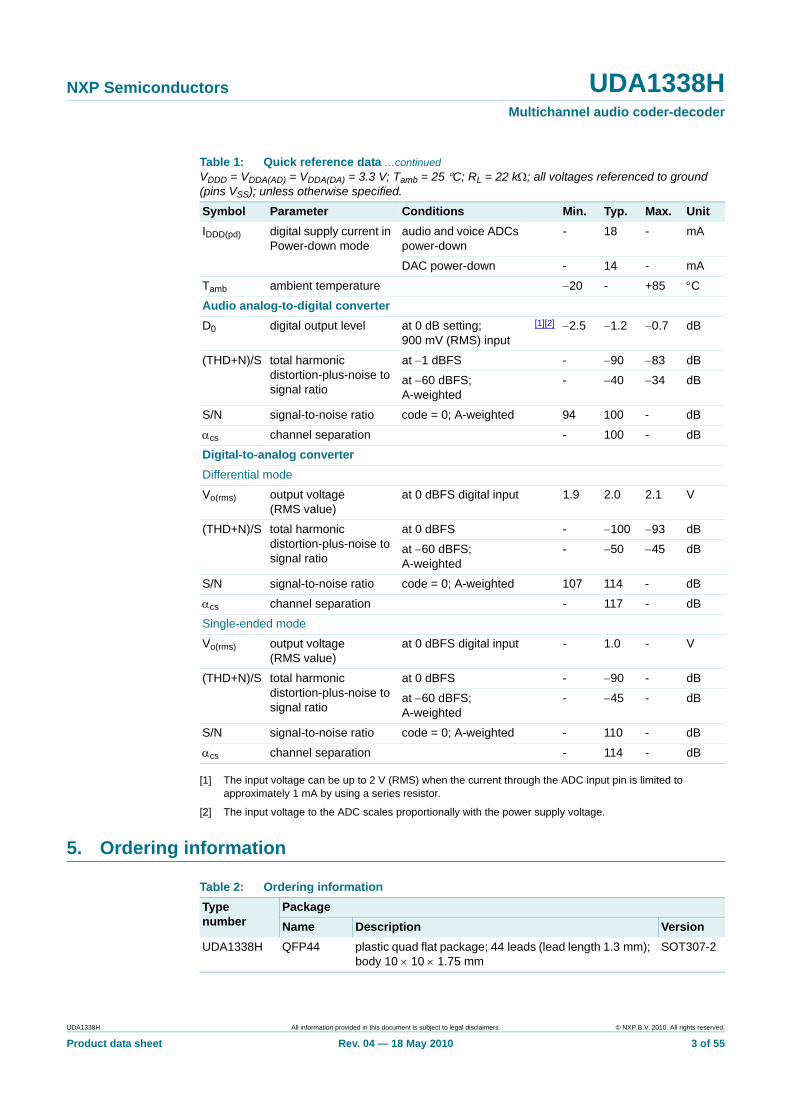
8.12 Voice digital interfaceThe following voice formats can be selected via the microcontroller interface:
• I2S-bus format with data word length of up to 20 bits. The left and the right channels contain the same data.
• Mono channel format with data word length of up to 20 bits
The formats are illustrated in Figure 9.
8.13 DSD modeThe UDA1338H can receive 2.8224 MHz DSD signals and generate 88.2 kHz multibit PCM signals as well as analog signal outputs. The configuration of the UDA1338H in the DSD mode is shown in Figure 10.
Fig 9. Voice digital interface formats
mgu587
MSB MSBB2
21≥ 81 2 3
LEFT
I2S-BUS FORMAT
WS
BCK
DATA
RIGHT
3 ≥ 8
MSB B2
MSB B2
21≥ 81 2 3
MONO CHANNEL FORMAT
WS
BCK
DATA MSB B2
Fig 10. DSD mode
mgu584
leftchannel
2.8224 MHzDSD
rightchannel
5.6448 MHz
88.2 kHz
BCKAD
DATADA3
DATADA2
WSAD
WSDA
88.2 kHz 22.5792 MHz5.6448 MHz
I2S-bus(left and right)
88.2 kHzPCM data
DATADA1DATAAD1 BCKDA SYSCLK
DAC+
−
INTERPOLATIONNOISE SHAPING
I2S-BUSINTERFACE 2
DECIMATIONFILTER
I2S-BUSINTERFACE 1
VOUT1N
VOUT1Pleftchannel
DAC+
−VOUT2N
VOUT2Prightchannel
analogoutput
UDA1338H All information provided in this document is subject to legal disclaimers. © NXP B.V. 2010. All rights reserved.
Product data sheet Rev. 04 — 18 May 2010 14 of 55

NXP Semiconductors UDA1338HMultichannel audio coder-decoder
8.14 Microcontroller interface modeThe microcontroller interface mode can be selected as shown in Table 11:
• L3-bus mode when pin I2C_L3 = LOW• I2C-bus mode when pin I2C_L3 = HIGH
All the features are accessible with the I2C-bus interface protocol as with the L3-bus interface protocol.
The detailed description of the device operation in the L3-bus mode and I2C-bus mode is given in Section 9 and Section 10, respectively.
9. L3-bus interface
9.1 GeneralThe UDA1338H has an L3-bus microcontroller interface and all the digital sound processing features and various system settings can be controlled by a microcontroller.
The exchange of data and control information between the microcontroller and the UDA1338H is LSB first and is accomplished through a serial hardware L3-bus interface comprising the following pins:
• MCCLK: clock line with signal L3CLOCK• MCDATA: data line with signal L3DATA• MCMODE: mode line with signal L3MODE.
The L3-bus format has two modes of operation:
• Address mode• Data transfer mode.
The address mode is used to select a device for a subsequent data transfer. The address mode is characterized by signal L3MODE = LOW and a burst of 8 pulses for signal L3CLOCK, accompanied by 8 bits; see Figure 11.
Table 11. Pin function in the L3-bus or I2C-bus modePin Level on pin I2C_L3
LOW HIGHL3-bus mode signal I2C-bus mode signal
MCCLK L3CLOCK SCL
MCDATA L3DATA SDA
MCMODE L3MODE QMUTE
Table 12: QMUTESignal QMUTE FunctionLOW no muting
HIGH muting
UDA1338H All information provided in this document is subject to legal disclaimers. © NXP B.V. 2010. All rights reserved.
Product data sheet Rev. 04 — 18 May 2010 15 of 55
NXP Semiconductors UDA1338HMultichannel audio coder-decoder
The data transfer mode is characterized by signal L3MODE = HIGH and is used to transfer one or more bytes representing a register address, instruction or data.
Basically, two types of data transfers can be defined:
• Write action: data transfer to the device• Read action: data transfer from the device.
9.2 Device addressingThe device address consists of one byte with:
• Data Operating Mode (DOM) bits 0 and 1 representing the type of data transfer; see Table 11.
• Address bit 2 to bit 7 representing a 6-bit device address. The address of the UDA1338H is 01 0100 (bit 2 to bit 7).
9.3 Register addressingAfter sending the device address (including DOM bits), indicating whether the information is to be read or written, one data byte is sent using bit 0 to indicate whether the information will be read or written and bit 1 to bit 7 for the destination register address.
Basically, there are 3 methods for register addressing:
1. Addressing for write data: bit 0 is logic 0 indicating a write action to the destination register, followed by bit 1 to bit 7 indicating the register address; see Figure 11.
2. Addressing for prepare read: bit is logic 1, indicating that data will be read from the register; see Figure 12.
3. Addressing for data read action. Here, the device returns a register address prior to sending data from that register. When bit 0 is logic 0, the register address is valid; when bit 0 is logic 1, the register address is invalid; see Figure 12.
Table 13: Selection of data transferDOM TransferBit 0 Bit 10 0 not used
1 0 not used
0 1 write data or prepare read
1 1 read data
UDA1338H All information provided in this document is subject to legal disclaimers. © NXP B.V. 2010. All rights reserved.
Product data sheet Rev. 04 — 18 May 2010 16 of 55

xxxxxxxxxxxxxxxxxxxxx xxxxxxxxxxxxxxxxxxxxxxxxxx xxxxxxx x x x xxxxxxxxxxxxxxxxxxxxxxxxxxxxxx xxxxxxxxxxxxxxxxxxx xx xx xxxxx xxxxxxxxxxxxxxxxxxxxxxxxxxx xxxxxxxxxxxxxxxxxxx xxxxxx xxxxxxxxxxxxxxxxxxxxxxxxxxxxxxxxxxx xxxxxxxxxxxx x x xxxxxxxxxxxxxxxxxxxxx xxxxxxxxxxxxxxxxxxxxxxxxxxxxxx xxxxx xxxxxxxxxxxxxxxxxxxxxxxxxxxxxxxxxxxxxxxxxxxxxxxxxx xxxxxxxx xxxxxxxxxxxxxxxxxxxxxxxxx xxxxxxxxxxxxxxxxxxxx xxx
UD
A1338H
Product data sh
NXP Sem
iconductorsU
DA
1338HM
ultichannel audio coder-decoder
mbl567
data byte 2
mbl565device
te 1 data byte 2
All information provided in this docum
ent is subject to legal disclaimers.
© N
XP B.V. 2010. All rights reserved.
eetR
ev. 04 — 18 M
ay 2010 17 of 55
Fig 11. Data write mode
L3CLOCK
L3MODE
L3DATA 0
write
device address
DOM bits
register addressdata byte 1
1 0
Fig 12. Data read mode
L3CLOCK
L3MODE
L3DATA 0
read valid/invalid
device address
prepare read sent by the
DOM bits
register address device addressrequesting
register addressdata by
1 1 1 0/11

NXP Semiconductors UDA1338HMultichannel audio coder-decoder
9.4 Data write modeThe data write mode is explained in the signal diagram of Figure 11. For writing data to a device, 4 bytes must be sent (see Table 14):
1. Byte 1 starting with ‘01’ for signalling the write action to the device, followed by the device address ‘01 0100’.
2. Byte 2 starting with a ‘0’ for signalling the write action, followed by 7 bits indicating the destination address in binary format with bit A6 being the MSB and bit A0 being the LSB.
3. Byte 3 with bit D15 being the MSB.4. Byte 4 with bit D0 being the LSB.
It should be noted that each time a new destination register address needs to be written, the device address must be sent again.
9.5 Data read modeTo read data from the device, a prepare read must first be done and then data read. The data read mode is explained in the signal diagram of Figure 12.
For reading data from a device, the following 6 bytes are involved (see Table 15):
1. Byte 1 with the device address, including ‘01’ for signalling the write action to the device.
2. Byte 2 is sent with the register address from which data needs to be read. This byte starts with a ‘1’, which indicates that there will be a read action from the register, followed by 7 bits for the destination address in binary format, with bit A6 being the MSB and bit A0 being the LSB.
3. Byte 3 with the device address, including ‘11’ is sent to the device. The ‘11’ indicates that the device must write data to the microcontroller.
4. Byte 4 sent by the device to the bus, with the (requested) register address and a flag bit indicating whether the requested register was valid (bit is logic 0) or invalid (bit is logic 1).
5. Byte 5 sent by the device to the bus, with the data information in binary format, with bit D15 being the MSB.
6. Byte 6 sent by the device to the bus, with the data information in binary format, with bit D0 being the LSB.
Table 14: L3-bus write dataByte L3-bus
modeAction First in time Latest in time
Bit 0 Bit 1 Bit 2 Bit 3 Bit 4 Bit 5 Bit 6 Bit 71 address device address 0 1 0 1 0 1 0 0
2 data transfer register address 0 A6 A5 A4 A3 A2 A1 A0
3 data transfer data byte 1 D15 D14 D13 D12 D11 D10 D9 D8
4 data transfer data byte 2 D7 D6 D5 D4 D3 D2 D1 D0
UDA1338H All information provided in this document is subject to legal disclaimers. © NXP B.V. 2010. All rights reserved.
Product data sheet Rev. 04 — 18 May 2010 18 of 55

NXP Semiconductors UDA1338HMultichannel audio coder-decoder
10. I2C-bus interface
10.1 GeneralThe UDA1338H has an I2C-bus microcontroller interface. All the features are accessible with the I2C-bus interface protocol. In the I2C-bus mode, the DAC mute function is accessible via pin MCMODE with signal QMUTE.
The exchange of data and control information between the microcontroller and the UDA1338H is accomplished through a serial hardware interface comprising the following pins as shown in Table 11:
• MCCLK: clock line with signal SCL• MCDATA: data line with signal SDA.
10.2 Characteristics of the I2C-busThe bus is for 2-way, 2-line communication between different ICs or modules. The two lines are a serial data line (SDA) and a serial clock line (SCL). Both lines must be connected to the supply voltage VDD via a pull-up resistor when connected to the output stages of a microcontroller. For a 400 kHz IC, the recommendation for this type of bus from Philips Semiconductors must be followed (e.g. up to loads of 200 pF on the bus a pull-up resistor can be used, between 200 pF and 400 pF a current source or switched resistor must be used). Data transfer can only be initiated when the bus is not busy.
10.3 Bit transferOne data bit is transferred during each clock pulse; see Figure 13. The data on the SDA line must remain stable during the HIGH period of the clock pulse as changes in the data line at this time will be interpreted as control signals. The maximum clock frequency is 400 kHz.
To be able to run on this high frequency, all the inputs and outputs connected to this bus must be designed for this high-speed I2C-bus according to the Philips specification.
Table 15: L3-bus read dataByte L3-bus
modeAction First in time Latest in time
Bit 0 Bit 1 Bit 2 Bit 3 Bit 4 Bit 5 Bit 6 Bit 71 address device address 0 1 0 1 0 1 0 0
2 data transfer register address 1 A6 A5 A4 A3 A2 A1 A0
3 address device address 1 1 0 1 0 1 0 0
4 data transfer register address 0 or 1 A6 A5 A4 A3 A2 A1 A0
5 data transfer data byte 1 D15 D14 D13 D12 D11 D10 D9 D8
6 data transfer data byte 2 D7 D6 D5 D4 D3 D2 D1 D0
UDA1338H All information provided in this document is subject to legal disclaimers. © NXP B.V. 2010. All rights reserved.
Product data sheet Rev. 04 — 18 May 2010 19 of 55

NXP Semiconductors UDA1338HMultichannel audio coder-decoder
10.4 Byte transferEach byte (8 bits) is transferred with the MSB first; see Table 16.
10.5 Data transferA device generating a message is a transmitter; a device receiving a message is the receiver. The device that controls the message is the master and the devices which are controlled by the master are the slaves.
10.6 Start and stop conditionsBoth data and clock line will remain HIGH when the bus is not busy. A HIGH-to-LOW transition of the data line, while the clock is HIGH, is defined as a start condition (S); see Figure 14. A LOW-to-HIGH transition of the data line while the clock is HIGH is defined as a stop condition (P).
10.7 AcknowledgmentThe number of data bits transferred between the start and stop conditions from the transmitter to receiver is not limited. Each byte of eight bits is followed by one acknowledge bit; see Figure 15. At the acknowledge bit the data line is released by the master and the master generates an extra acknowledge related clock pulse.
A slave receiver which is addressed, must generate an acknowledge after the reception of each byte. Also a master must generate an acknowledge after the reception of each byte that has been clocked out of the slave transmitter.
The device that acknowledges has to pull down the SDA line during the acknowledge clock pulse, so the SDA line is stable LOW during the HIGH period of the acknowledge related clock pulse. Set-up and hold times must be taken into account. A master receiver must signal an end of data to the transmitter by not generating an acknowledge on the last byte that has been clocked out of the slave. In this event, the transmitter must leave the data line HIGH to enable the master to generate a stop condition.
Table 16: Byte transferMSB Bit number LSB7 6 5 4 3 2 1 0
Fig 13. Bit transfer on the I2C-bus
mbc621
data linestable;
data valid
changeof dataallowed
SDA
SCL
UDA1338H All information provided in this document is subject to legal disclaimers. © NXP B.V. 2010. All rights reserved.
Product data sheet Rev. 04 — 18 May 2010 20 of 55

NXP Semiconductors UDA1338HMultichannel audio coder-decoder
10.8 Device addressBefore any data is transmitted on the I2C-bus, the device which should respond is addressed first. The addressing is always done with byte 1 transmitted after the start procedure. The UDA1338H acts as a slave receiver or a slave transmitter.
Therefore, the clock signal SCL is only an input signal. The data signal SDA is a bidirectional line. The UDA1338H device address is shown in Table 17.
10.9 Register addressThe register addresses in the I2C-bus mode are the same as in the L3-bus mode. The register addresses are defined in Section 11.
Fig 14. START and STOP conditions on the I2C-bus
Fig 15. Acknowledge on the I2C-bus
mbc622
SDA
SCLP
STOP condition
SDA
SCLS
START condition
mbc602
S
STARTcondition
9821
clock pulse foracknowledgement
not acknowledge
acknowledge
data outputby transmitter
data outputby receiver
SCL frommaster
Table 17. I2C-bus device address of UDA1338HDevice address R/WA6 A5 A4 A3 A2 A1 A00 0 1 1 0 0 0 0/1
UDA1338H All information provided in this document is subject to legal disclaimers. © NXP B.V. 2010. All rights reserved.
Product data sheet Rev. 04 — 18 May 2010 21 of 55

NXP Semiconductors UDA1338HMultichannel audio coder-decoder
10.10 Write and read dataThe I2C-bus configurations for a write and read cycle are shown in Table 18 and Table 19, respectively.
The write cycle is used to write groups of two bytes to the internal registers for the settings. It is also possible to read the registers for the device status information.
10.11 Write cycleThe I2C-bus configuration for a write cycle is shown in Table 18. The write cycle is used to write the data to the internal registers. The device and register addresses are one byte each, the setting data is always a pair of two bytes.
The format of the write cycle is as follows:
1. The microcontroller starts with a start condition (S).2. The first byte (8 bits) contains the device address ‘0011 000’ and a logic 0 (write) for
the R/W bit.3. This is followed by an acknowledge (A) from the UDA1338H.4. After this the microcontroller writes the 8-bit register address (ADDR) where the
writing of the register content of the UDA1338H must start.5. The UDA1338H acknowledges this register address (A).6. The microcontroller sends 2 bytes data with the Most Significant (MS) byte first and
then the Least Significant (LS) byte. After each byte an acknowledge is followed from the UDA1338H.
7. If repeated groups of 2 bytes data are transmitted, then the register address is auto incremented. After each byte an acknowledge is followed from the UDA1338H.
8. Finally, the UDA1338H frees the I2C-bus and the microcontroller can generate a stop condition (P).
[1] Auto increment of register address.
10.12 Read cycleThe read cycle is used to read the data values from the internal registers. The I2C-bus configuration for a read cycle is shown in Table 19.
The format of the read cycle is as follows:
1. The microcontroller starts with a start condition (S).2. The first byte (8 bits) contains the device address ‘0011 000’ and a logic 0 (write) for
the R/W bit.3. This is followed by an acknowledge (A) from the UDA1338H.
Table 18. Master transmitter writes to UDA1338H registers in the I2C-bus modeDevice address
R/W
Register address
data 1 DATA 2[1] DATA n[1]
S 0011 000 0 A ADDR A MS1 A LS1 A MS2 A LS2 A MSn A LSn A P
acknowledge from UDA1338H
UDA1338H All information provided in this document is subject to legal disclaimers. © NXP B.V. 2010. All rights reserved.
Product data sheet Rev. 04 — 18 May 2010 22 of 55

NXP Semiconductors UDA1338HMultichannel audio coder-decoder
4. After this the microcontroller writes the 8-bit register address (ADDR) where the reading of the register content of the UDA1338H must start.
5. The UDA1338H acknowledges this register address.6. Then the microcontroller generates a repeated start (Sr).7. Then the microcontroller generates the device address ‘0011 000’ again, but this time
followed by a logic 1 (read) of the R/W bit. An acknowledge is followed from the UDA1338H.
8. The UDA1338H sends 2 bytes data with the Most Significant (MS) byte first and then the Least Significant (LS) byte. After each byte an acknowledge is followed from the microcontroller (master).
9. If repeated groups of 2 bytes are transmitted, then the register address is auto incremented. After each byte an acknowledge is followed from the microcontroller.
10.The microcontroller stops this cycle by generating a negative acknowledge (NA).11. Finally, the UDA1338H frees the I2C-bus and the microcontroller can generate a stop
condition (P).
[1] Auto increment of register address.
11. Register mapping
In this chapter the register addressing and mapping of the microcontroller interface of the UDA1338H is given.
In Table 20 an overview of the register mapping is given.
In Table 21 the actual register mapping is given and the register definitions are explained in Section 11.3 to Section 11.14.
11.1 Address mapping
Table 19. Master transmitter reads from the UDA1338H registers in the I2C-bus modeDevice address
R/W
Register address
Device address
R/W
data 1 DATA 2[1] DATA n[1]
S 0011 000 0 A ADDR A Sr 0011 000 1 A MS1 A LS1 A MS2 A LS2 A MSn A LSn NA P
acknowledge from UDA1338H acknowledge from master
Table 20: Overview of register mappingAddress FunctionSystem settings00h system
01h audio ADC and DAC subsystem
02h voice ADC system
Status (read out registers)0Fh status outputs
Interpolator settings10h DAC channel and feature selection
11h DAC feature control
UDA1338H All information provided in this document is subject to legal disclaimers. © NXP B.V. 2010. All rights reserved.
Product data sheet Rev. 04 — 18 May 2010 23 of 55

NXP Semiconductors UDA1338HMultichannel audio coder-decoder
12h DAC channel 1
13h DAC channel 2
14h DAC channel 3
15h DAC channel 4
16h DAC channel 5
17h DAC channel 6
18h DAC mixing channel 1
19h DAC mixing channel 2
1Ah DAC mixing channel 3
1Bh DAC mixing channel 4
1Ch DAC mixing channel 5
1Dh DAC mixing channel 6
ADC input amplifier gain settings20h audio ADC input amplifier gain
21h voice ADC input amplifier gain
Supplemental settings30h supplemental settings 1
31h supplemental settings 2
Table 20: Overview of register mapping …continued
Address Function
UDA1338H All information provided in this document is subject to legal disclaimers. © NXP B.V. 2010. All rights reserved.
Product data sheet Rev. 04 — 18 May 2010 24 of 55

xxxxxxxxxxxxxxxxxxxxx xxxxxxxxxxxxxxxxxxxxxxxxxx xxxxxxx x x x xxxxxxxxxxxxxxxxxxxxxxxxxxxxxx xxxxxxxxxxxxxxxxxxx xx xx xxxxx xxxxxxxxxxxxxxxxxxxxxxxxxxx xxxxxxxxxxxxxxxxxxx xxxxxx xxxxxxxxxxxxxxxxxxxxxxxxxxxxxxxxxxx xxxxxxxxxxxx x x xxxxxxxxxxxxxxxxxxxxx xxxxxxxxxxxxxxxxxxxxxxxxxxxxxx xxxxx xxxxxxxxxxxxxxxxxxxxxxxxxxxxxxxxxxxxxxxxxxxxxxxxxx xxxxxxxx xxxxxxxxxxxxxxxxxxxxxxxxx xxxxxxxxxxxxxxxxxxxx xxx
UD
A1338H
Product data sh
NXP Sem
iconductorsU
DA
1338HM
ultichannel audio coder-decoder
11.2 Register mapping
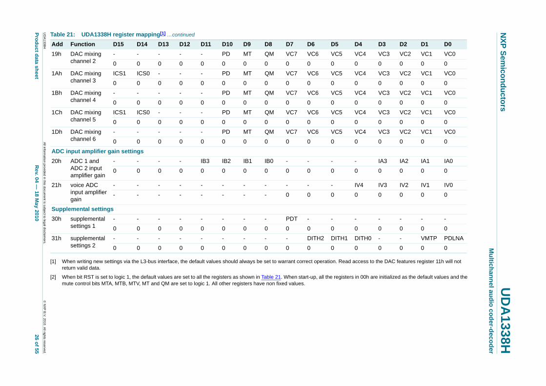
Table 21: UDA1338H register mapping[1]
Add Function D15 D14 D13 D12 D11 D10 D9 D8 D7 D6 D5 D4 D3 D2 D1 D0
0 ACE ADP DCE DAP
1 0 1 0
S1 DIS0 DIF2 DIF1 DIF0
0 0 0 0
1 VH0 PVA MTV VIF
1 0 0 0
1 AS0 DS2 DS1 DS0
4 CS3 CS2 CS1 CS0
0 0 0 0
4 VC3 VC2 VC1 VC0
0 0 0 0
4 VC3 VC2 VC1 VC0
0 0 0 0
4 VC3 VC2 VC1 VC0
0 0 0 0
4 VC3 VC2 VC1 VC0
0 0 0 0
4 VC3 VC2 VC1 VC0
0 0 0 0
4 VC3 VC2 VC1 VC0
0 0 0 0
4 VC3 VC2 VC1 VC0
0 0 0 0
4 VC3 VC2 VC1 VC0
0 0 0 0
All information provided in this docum
ent is subject to legal disclaimers.
© N
XP B.V. 2010. All rights reserved.
eetR
ev. 04 — 18 M
ay 2010 25 of 55
System settings00h system RST[2] VFS1 VFS0 VCE VAP DSD SC1 SC0 OP1 OP0 FS1 FS
- 0 0 1 0 0 0 0 0 0 0 1
01h audio ADC and DAC subsystem
DC PAB PAA MTB MTA AIF2 AIF1 AIF0 DAG FIL DVD DI
1 0 0 0 0 0 0 0 0 0 0 0
02h voice ADC system
- - - - - - - - BCK1 BCK0 WSM VH
0 0 0 0 0 0 0 0 0 1 1 0
Status (read out only)0Fh status outputs - - - - - - - - - - VS AS
Interpolator settings10h DAC channel
and feature selection
MIX1 MIX0 MC5 MC4 MC3 MC2 MC1 MC0 SEL1 SEL0 CS5 CS
0 0 0 0 0 0 0 0 0 0 0 0
11h DAC feature control
ICS1 ICS0 DE2 DE1 DE0 PD MT QM VC7 VC6 VC5 VC
0 0 0 0 0 0 0 0 0 0 0 0
12h DAC channel 1
ICS1 ICS0 DE2 DE1 DE0 PD MT QM VC7 VC6 VC5 VC
0 0 0 0 0 0 0 0 0 0 0 0
13h DAC channel 2
- - DE2 DE1 DE0 PD MT QM VC7 VC6 VC5 VC
0 0 0 0 0 0 0 0 0 0 0 0
14h DAC channel 3
ICS1 ICS0 DE2 DE1 DE0 PD MT QM VC7 VC6 VC5 VC
0 0 0 0 0 0 0 0 0 0 0 0
15h DAC channel 4
- - DE2 DE1 DE0 PD MT QM VC7 VC6 VC5 VC
0 0 0 0 0 0 0 0 0 0 0 0
16h DAC channel 5
ICS1 ICS0 DE2 DE1 DE0 PD MT QM VC7 VC6 VC5 VC
0 0 0 0 0 0 0 0 0 0 0 0
17h DAC channel 6
- - DE2 DE1 DE0 PD MT QM VC7 VC6 VC5 VC
0 0 0 0 0 0 0 0 0 0 0 0
18h DAC mixing channel 1
ICS1 ICS0 - - - PD MT QM VC7 VC6 VC5 VC
0 0 0 0 0 0 0 0 0 0 0 0
xxxxxxxxxxxxxxxxxxxxx xxxxxxxxxxxxxxxxxxxxxxxxxx xxxxxxx x x x xxxxxxxxxxxxxxxxxxxxxxxxxxxxxx xxxxxxxxxxxxxxxxxxx xx xx xxxxx xxxxxxxxxxxxxxxxxxxxxxxxxxx xxxxxxxxxxxxxxxxxxx xxxxxx xxxxxxxxxxxxxxxxxxxxxxxxxxxxxxxxxxx xxxxxxxxxxxx x x xxxxxxxxxxxxxxxxxxxxx xxxxxxxxxxxxxxxxxxxxxxxxxxxxxx xxxxx xxxxxxxxxxxxxxxxxxxxxxxxxxxxxxxxxxxxxxxxxxxxxxxxxx xxxxxxxx xxxxxxxxxxxxxxxxxxxxxxxxx xxxxxxxxxxxxxxxxxxxx xxx
UD
A1338H
Product data sh
NXP Sem
iconductorsU
DA
1338HM
ultichannel audio coder-decoder
ess to the DAC features register 11h will not
00h are initialized as the default values and the
19h DAC mixing channel 2
- - - - - PD MT QM VC7 VC6 VC5 VC4 VC3 VC2 VC1 VC0
0 0 0 0 0 0 0 0 0 0 0 0 0 0 0 0
4 VC3 VC2 VC1 VC0
0 0 0 0
4 VC3 VC2 VC1 VC0
0 0 0 0
4 VC3 VC2 VC1 VC0
0 0 0 0
4 VC3 VC2 VC1 VC0
0 0 0 0
IA3 IA2 IA1 IA0
0 0 0 0
4 IV3 IV2 IV1 IV0
0 0 0 0
- - - -
0 0 0 0
TH0 - - VMTP PDLNA
0 0 0 0
Table 21: UDA1338H register mapping[1] …continued
Add Function D15 D14 D13 D12 D11 D10 D9 D8 D7 D6 D5 D4 D3 D2 D1 D0
All information provided in this docum
ent is subject to legal disclaimers.
© N
XP B.V. 2010. All rights reserved.
eetR
ev. 04 — 18 M
ay 2010 26 of 55
[1] When writing new settings via the L3-bus interface, the default values should always be set to warrant correct operation. Read accreturn valid data.
[2] When bit RST is set to logic 1, the default values are set to all the registers as shown in Table 21. When start-up, all the registers in mute control bits MTA, MTB, MTV, MT and QM are set to logic 1. All other registers have non fixed values.
1Ah DAC mixing channel 3
ICS1 ICS0 - - - PD MT QM VC7 VC6 VC5 VC
0 0 0 0 0 0 0 0 0 0 0 0
1Bh DAC mixing channel 4
- - - - - PD MT QM VC7 VC6 VC5 VC
0 0 0 0 0 0 0 0 0 0 0 0
1Ch DAC mixing channel 5
ICS1 ICS0 - - - PD MT QM VC7 VC6 VC5 VC
0 0 0 0 0 0 0 0 0 0 0 0
1Dh DAC mixing channel 6
- - - - - PD MT QM VC7 VC6 VC5 VC
0 0 0 0 0 0 0 0 0 0 0 0
ADC input amplifier gain settings20h ADC 1 and
ADC 2 input amplifier gain
- - - - IB3 IB2 IB1 IB0 - - - -
0 0 0 0 0 0 0 0 0 0 0 0
21h voice ADC input amplifier gain
- - - - - - - - - - - IV
- - - - - - - - 0 0 0 0
Supplemental settings30h supplemental
settings 1- - - - - - - - PDT - - -
0 0 0 0 0 0 0 0 0 0 0 0
31h supplemental settings 2
- - - - - - - - - DITH2 DITH1 DI
0 0 0 0 0 0 0 0 0 0 0 0
NXP Semiconductors UDA1338HMultichannel audio coder-decoder
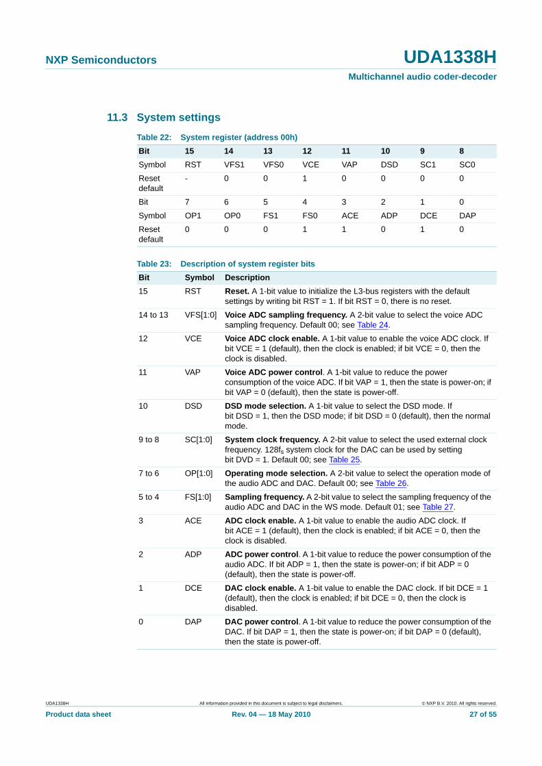
11.3 System settings
Table 22: System register (address 00h)Bit 15 14 13 12 11 10 9 8Symbol RST VFS1 VFS0 VCE VAP DSD SC1 SC0
Reset default
- 0 0 1 0 0 0 0
Bit 7 6 5 4 3 2 1 0
Symbol OP1 OP0 FS1 FS0 ACE ADP DCE DAP
Reset default
0 0 0 1 1 0 1 0
Table 23: Description of system register bitsBit Symbol Description15 RST Reset. A 1-bit value to initialize the L3-bus registers with the default
settings by writing bit RST = 1. If bit RST = 0, there is no reset.
14 to 13 VFS[1:0] Voice ADC sampling frequency. A 2-bit value to select the voice ADC sampling frequency. Default 00; see Table 24.
12 VCE Voice ADC clock enable. A 1-bit value to enable the voice ADC clock. If bit VCE = 1 (default), then the clock is enabled; if bit VCE = 0, then the clock is disabled.
11 VAP Voice ADC power control. A 1-bit value to reduce the power consumption of the voice ADC. If bit VAP = 1, then the state is power-on; if bit VAP = 0 (default), then the state is power-off.
10 DSD DSD mode selection. A 1-bit value to select the DSD mode. If bit DSD = 1, then the DSD mode; if bit DSD = 0 (default), then the normal mode.
9 to 8 SC[1:0] System clock frequency. A 2-bit value to select the used external clock frequency. 128fs system clock for the DAC can be used by setting bit DVD = 1. Default 00; see Table 25.
7 to 6 OP[1:0] Operating mode selection. A 2-bit value to select the operation mode of the audio ADC and DAC. Default 00; see Table 26.
5 to 4 FS[1:0] Sampling frequency. A 2-bit value to select the sampling frequency of the audio ADC and DAC in the WS mode. Default 01; see Table 27.
3 ACE ADC clock enable. A 1-bit value to enable the audio ADC clock. If bit ACE = 1 (default), then the clock is enabled; if bit ACE = 0, then the clock is disabled.
2 ADP ADC power control. A 1-bit value to reduce the power consumption of the audio ADC. If bit ADP = 1, then the state is power-on; if bit ADP = 0 (default), then the state is power-off.
1 DCE DAC clock enable. A 1-bit value to enable the DAC clock. If bit DCE = 1 (default), then the clock is enabled; if bit DCE = 0, then the clock is disabled.
0 DAP DAC power control. A 1-bit value to reduce the power consumption of the DAC. If bit DAP = 1, then the state is power-on; if bit DAP = 0 (default), then the state is power-off.
UDA1338H All information provided in this document is subject to legal disclaimers. © NXP B.V. 2010. All rights reserved.
Product data sheet Rev. 04 — 18 May 2010 27 of 55

NXP Semiconductors UDA1338HMultichannel audio coder-decoder
11.4 Audio ADC and DAC subsystem settings
Table 24: Voice ADC sampling frequency bitsVFS1 VFS0 Function0 0 6.25 kHz to 12.5 kHz (default)
0 1 12.5 kHz to 25 kHz
1 0 25 kHz to 50 kHz
1 1 reserved
Table 25: System clock frequency bitsSC1 SC0 ADC DAC Remark
Bit DVD = 0 Bit DVD = 10 0 256fs 256fs 128fs default
0 1 384fs 384fs 192fs1 0 512fs 512fs 256fs1 1 768fs 768fs 384fs
Table 26: Operating mode bitsOP1 OP0 ADC mode DAC mode Remark0 0 SYSCLK (256fs, 384fs, 512fs or
768fs)SYSCLK (128fs, 256fs, 384fs, 512fs or 768fs)
default
0 1 SYSCLK (256fs, 384fs, 512fs or 768fs)
WSDA (1fs)
1 0 WSAD (1fs) SYSCLK (128fs, 256fs, 384fs, 512fs or 768fs)
1 1 WSDA (1fs) WSDA (1fs)
Table 27: Audio ADC and DAC sampling frequency bitsFS1 FS0 Function0 0 12.5 kHz to 25 kHz
0 1 25 kHz to 50 kHz (default)
1 0 50 kHz to 100 kHz
1 1 100 kHz to 200 kHz
Table 28: Audio ADC and DAC subsystem register (address 01h)Bit 15 14 13 12 11 10 9 8Symbol DC PAB PAA MTB MTA AIF2 AIF1 AIF0
Reset default
1 0 0 0 0 0 0 0
Bit 7 6 5 4 3 2 1 0
Symbol DAG FIL DVD DIS1 DIS0 DIF2 DIF1 DIF0
Reset default
0 0 0 0 0 0 0 0
UDA1338H All information provided in this document is subject to legal disclaimers. © NXP B.V. 2010. All rights reserved.
Product data sheet Rev. 04 — 18 May 2010 28 of 55

NXP Semiconductors UDA1338HMultichannel audio coder-decoder
Table 29: Description of the audio ADC and DAC subsystem register bitsBit Symbol Description15 DC ADC DC-filter. A 1-bit value to enable the digital DC-filter of the ADC. If
bit DC = 1 (default), then the DC-filtering is active; if bit DC = 0, then there is no DC-filtering.
14 PAB Polarity ADC 2 control. A 1-bit value to control the ADC 2 polarity. If bit PAB = 1, then the polarity is inverted; if bit PAB = 0 (default), then the polarity is non-inverted.
13 PAA Polarity ADC 1 control. A 1-bit value to control the ADC 1 polarity. If bit PAA = 1, then the polarity is inverted; if bit PAA = 0 (default), then the polarity is non-inverted.
12 MTB Mute ADC 2. A 1-bit value to enable the digital mute of ADC 2. If bit MTB = 1, then ADC 2 is soft muted; if bit MTB = 0 (default), then ADC 2 is not muted.
11 MTA Mute ADC 1. A 1-bit value to enable the digital mute of ADC 1. If bit MTA = 1, then ADC 1 is soft muted; if bit MTA = 0 (default), then ADC 1 is not muted.
10 to 8 AIF[2:0] ADC output data interface format. A 3-bit value to select the used data format to the I2S-bus ADC output interface. Default 000; see Table 30.
7 DAG DAC gain switch. A 1-bit value to select the DAC gain. If bit DAG = 1, then the gain is 6 dB; if bit DAG = 0 (default), then the gain is 0 dB.
6 FIL Filter selection. A 1-bit value to select the interpolation filter characteristics. If bit FIL = 1, then slow roll-off; if bit FIL = 0 (default), then sharp roll-off.
5 DVD 192 kHz sampling mode selection. A 1-bit value to select the oversampling rate of the noise shaper. The 64fs rate is used for 192 kHz and 176.4 kHz sampling frequencies. If 7-bit DVD = 1, then 64fs rate is selected (192 kHz sampling mode); if bit DVD = 0 (default), then 128fs rate is selected.
4 to 3 DIS[1:0] Data interface selection. A 2-bit value to select the data interface connection. Default 00; see Table 31.
2 to 0 DIF[2:0] DAC input data interface format. A 3-bit value to select the used data format to the I2S-bus DAC input interface. Default 000; see Table 30.
Table 30: Data interface format bitsAIF2 AIF1 AIF0 FunctionDIF2 DIF1 DIF00 0 0 I2S-bus format (default)
0 0 1 LSB-justified format, 16 bits
0 1 0 LSB-justified format, 20 bits
0 1 1 LSB-justified format, 24 bits
1 0 0 MSB-justified format
1 0 1 multichannel format, 20 bits
1 1 0 multichannel format, 24 bits (format 1)
1 1 1 multichannel format, 24 bits (format 2)
UDA1338H All information provided in this document is subject to legal disclaimers. © NXP B.V. 2010. All rights reserved.
Product data sheet Rev. 04 — 18 May 2010 29 of 55

NXP Semiconductors UDA1338HMultichannel audio coder-decoder
11.5 Voice ADC system settings
Table 31: Data interface selection bitsDIS1 DIS0 Input to DAC0 0 DATADA1 to DAC channel 1 and channel 2, DATADA2 to DAC channel 3
and channel 4, and DATADA3 to DAC channel 5 and channel 6 (default)
0 1 DATADA1 to DAC channel 1 to channel 6
1 0 DATADA2 to DAC channel 1 to channel 6
1 1 DATADA3 to DAC channel 1 to channel 6
Table 32: Voice ADC system register (address 02h)Bit 15 14 13 12 11 10 9 8Symbol - - - - - - - -
Reset default
0 0 0 0 0 0 0 0
Bit 7 6 5 4 3 2 1 0
Symbol BCK1 BCK0 WSM VH1 VH0 PVA MTV VIF
Reset default
0 1 1 0 1 0 0 0
Table 33: Description of the voice ADC system register bitsBit Symbol Description15 to 8 - default 0000 0000
7 to 6 BCK[1:0] BCK frequency of voice ADC. A 2-bit value to select the BCK frequency of the voice ADC in the WSV-out mode. Default 01; see Table 34.
5 WSM WSV mode selection. A 1-bit value to select the WSV mode of the voice ADC. If bit WSM = 1 (default), then WSV-in mode; if bit WSM = 0, then WSV-out mode.
4 to 3 VH[1:0] Voice ADC high-pass filter setting. A 2-bit value to enable the high-pass filter of the voice ADC. Default 01; see Table 35.
2 PVA Polarity voice ADC control. A 1-bit value to control the voice ADC polarity. If bit PVA = 1, then the polarity is inverted; if bit PVA = 0 (default), then the polarity is non-inverted.
1 MTV Mute voice ADC. A 1-bit value to enable the digital mute of the voice ADC. If bit MTV = 1, then the voice ADC is soft muted; if bit MTV = 0 (default), then the voice ADC is not muted.
0 VIF Voice ADC interface format. A 1-bit value to select the data interface format of the voice ADC. If bit VIF = 1, then mono-channel format; if bit VIF = 0 (default), then I2S-bus format.
Table 34: BCK frequency of voice ADC bitsBCK1 BCK0 Function0 0 32fs0 1 64fs (default)
1 0 128fs1 1 256fs
UDA1338H All information provided in this document is subject to legal disclaimers. © NXP B.V. 2010. All rights reserved.
Product data sheet Rev. 04 — 18 May 2010 30 of 55

NXP Semiconductors UDA1338HMultichannel audio coder-decoder
11.6 Status output register (read only)
Table 35: Voice ADC high-pass filter setting bitsVH1 VH0 Function0 0 high-pass filter off
0 1 fc = 0.00008fs (default)
1 0 fc = 0.0125fs1 1 fc = 0.025fs
Table 36: Status output register (address 0Fh)Bit 15 14 13 12 11 10 9 8Symbol - - - - - - - -
Bit 7 6 5 4 3 2 1 0
Symbol - - VS AS1 AS0 DS2 DS1 DS0
Table 37: Description of status output register bitsBit Symbol Description15 to 6 - not used
5 VS Voice ADC status. A 1-bit value to indicate the hard mute status of the voice ADC. If bit VS = 1, then power-down is ready and the clock may be disabled; if bit VS = 0, then power-down is not ready and the clock should not be disabled.
4 AS1 ADC 2 status. A 1-bit value to indicate the hard mute status of ADC 2. If bit AS1 = 1, then power-down is ready and the clock may be disabled; if bit AS1 = 0, then power-down is not ready and the clock should not be disabled.
3 AS0 ADC 1 status. A 1-bit value to indicate the hard mute status of ADC 1. If bit AS0 = 1, then power-down is ready and the clock may be disabled; if bit AS0 = 0, then power-down is not ready and the clock should not be disabled.
2 DS2 DAC channel 5 and channel 6 status. A 1-bit value to indicate the hard mute status of DAC channel 5 and channel 6. If bit DS2 = 1, then power-down is ready and the clock may be disabled; if bit DS2 = 0, then power-down is not ready and the clock should not be disabled.
1 DS1 DAC channel 3 and channel 4 status. A 1-bit value to indicate the hard mute status of DAC channel 3 and channel 4. If bit DS1= 1, then power-down is ready and the clock may be disabled; if bit DS1 = 0, then power-down is not ready and the clock should not be disabled.
0 DS0 DAC channel 1 and channel 2 status. A 1-bit value to indicate the hard mute status of DAC channel 1 and channel 2. If bit DS0 = 1, then power-down is ready and the clock may be disabled; if bit DS0 = 0, then power-down is not ready and the clock should not be disabled.
UDA1338H All information provided in this document is subject to legal disclaimers. © NXP B.V. 2010. All rights reserved.
Product data sheet Rev. 04 — 18 May 2010 31 of 55

NXP Semiconductors UDA1338HMultichannel audio coder-decoder
11.7 DAC channel selection
Table 38: DAC channel select register (address 10h)Bit 15 14 13 12 11 10 9 8Symbol MIX1 MIX0 MC5 MC4 MC3 MC2 MC1 MC0
Reset default
0 0 0 0 0 0 0 0
Bit 7 6 5 4 3 2 1 0
Symbol SEL1 SEL0 CS5 CS4 CS3 CS2 CS1 CS0
Reset default
0 0 0 0 0 0 0 0
Table 39: Description of DAC channel select register bitsBit Symbol Description15 to 14 MIX[1:0] DAC mixer setting. A 2-bit value to enable the DAC mixer. Default 00;
see Table 40.
13 to 8 MC[5:0] DAC mixing channel selection. A group of 6 enable bits to make DAC mixing channels ready for receiving feature settings through register address 11H. Only selected registers accept new settings. Default 00 0000 (no channel ready); see Table 41.
7 and 6 SEL[1:0] Feature selection. A 2-bit value to select the features to be set through register address 11H. When the feature settings are written, only selected feature settings are changed and non selected features are kept unchanged. Default 00; see Table 42.
5 to 0 CS[5:0] DAC channel selection. A group of 6 enable bits to make DAC channel ready for receiving feature settings through register address 11H. Default 00 0000 (no channel ready); see Table 41.
Table 40: DAC mixer setting bitsMIX1 MIX0 Function0 0 no mixing (default)
0 1 no mixing
1 0 mixing ADC 1
1 1 mixing ADC 2
Table 41: DAC channel and mixing channel selection bitsMC5 MC4 MC3 MC2 MC1 MC0 FunctionCS5 CS4 CS3 CS2 CS1 CS00 0 0 0 0 1 channel 1 selected
: : : : : :
0 0 1 0 1 0 channel 2 and channel 4 selected
: : : : : :
1 1 1 1 1 1 all channels selected
UDA1338H All information provided in this document is subject to legal disclaimers. © NXP B.V. 2010. All rights reserved.
Product data sheet Rev. 04 — 18 May 2010 32 of 55

NXP Semiconductors UDA1338HMultichannel audio coder-decoder
11.8 DAC features settings
Table 42: Feature selection bitsSEL1 SEL0 Function0 0 all features (default)
0 1 volume
1 0 mute and quick mute
1 1 de-emphasis, polarity and input channel selection
Table 43: DAC features register (addresses 11h)Bit 15 14 13 12 11 10 9 8Symbol ICS1 ICS0 DE2 DE1 DE0 PD MT QM
Reset default
0 0 0 0 0 0 0 0
Bit 7 6 5 4 3 2 1 0
Symbol VC7 VC6 VC5 VC4 VC3 VC2 VC1 VC0
Reset default
0 0 0 0 0 0 0 0
Table 44: Description of DAC features register bitsBit Symbol Description15 to 14 ICS[1:0] Input channel selection. A 2-bit value to select the input channels. As the
controlled channels are paired off, this 2-bit value must be written to each odd channel register. Default 00; see Table 45.
13 to 11 DE[2:0] De-emphasis setting. A 3-bit value to enable the digital de-emphasis filter. Default 000; see Table 46.
10 PD Polarity DAC control. A 1-bit value to control the DAC polarity. If bit PD = 1, then the polarity is inverted; if bit PD = 0 (default), then the polarity is non-inverted.
9 MT Muting. A 1-bit value to enable the digital mute. All the DAC outputs are muted at start-up. It is necessary to explicitly switch off for the audio output by means of bit MT. If bit MT = 1 (start-up), then muting; if bit MT = 0 (default), then no muting.
8 QM Quick mute. A 1-bit value to set the quick mute mode. If bit QM = 1 (start-up), then quick mute mode; if bit QM = 0 (default), then soft mute mode.
7 to 0 VC[7:0] Interpolator volume control. An 8-bit value to program the volume attenuation of each channel. The range is from 0 to −53 dB in steps of 0.25 dB, from −53 dB to −80 dB in steps of 3 dB and −∞ dB. Default 0000 0000; see Table 47.
UDA1338H All information provided in this document is subject to legal disclaimers. © NXP B.V. 2010. All rights reserved.
Product data sheet Rev. 04 — 18 May 2010 33 of 55

NXP Semiconductors UDA1338HMultichannel audio coder-decoder
Table 45: Input channel selection bitsICS1 ICS0 Input to DAC output0 0 left channel input data to odd channel output; right channel input data to
even channel output
0 1 left channel input data to odd and even channel outputs
1 0 right channel input data to odd and even channel outputs
1 1 left channel input data to even channel output; right channel input data to odd channel output
Table 46: De-emphasis bitsDE2 DE1 DE0 Function0 0 0 no de-emphasis
(default)
0 0 1 de-emphasis of 32 kHz
0 1 0 de-emphasis of 44.1 kHz
0 1 1 de-emphasis of 48 kHz
1 0 0 de-emphasis of 96 kHz
1 0 1 not used
1 1 0 not used
1 1 1 not used
Table 47: Interpolator volume control bitsVC7 VC6 VC5 VC4 VC3 VC2 VC1 VC0 Volume (dB)0 0 0 0 0 0 0 0 0 (default)
0 0 0 0 0 0 0 1 −0.25
0 0 0 0 0 0 1 0 −0.50
0 0 0 0 0 0 1 1 −0.75
0 0 0 0 0 1 0 0 −1.00
0 0 0 0 0 1 0 1 −1.25
: : : : : : : : :
1 1 0 1 0 1 0 0 −53
1 1 0 1 1 0 0 0 −56
1 1 0 1 1 1 0 0 −59
1 1 1 0 0 0 0 0 −62
1 1 1 0 0 1 0 0 −65
1 1 1 0 1 0 0 0 −68
1 1 1 0 1 1 0 0 −71
1 1 1 1 0 0 0 0 −74
1 1 1 1 0 1 0 0 −77
1 1 1 1 1 0 0 0 −80
1 1 1 1 1 1 0 0 −∞
: : : : : : : : :
1 1 1 1 1 1 1 1 −∞
UDA1338H All information provided in this document is subject to legal disclaimers. © NXP B.V. 2010. All rights reserved.
Product data sheet Rev. 04 — 18 May 2010 34 of 55

NXP Semiconductors UDA1338HMultichannel audio coder-decoder
11.9 DAC channel 1 to channel 6 settingsAll the DAC features which are written in register 11h are copied into the odd channel registers.
All the DAC features which are written in register 11h are copied into the even channel registers, except the bits ICS[1:0].
11.10 DAC mixing channel settingsAll the DAC features which are written in register 11h are copied into the odd mixing channel registers, except the bits DE[2:0].
All the DAC features which are written in register 11h are copied into the even channel registers, except the bits ICS[1:0] and DE[2:0].
Table 48: DAC channel 1, 3 and 5 registers (addresses 12h, 14h and 16h)Bit 15 14 13 12 11 10 9 8Symbol ICS1 ICS0 DE2 DE1 DE0 PD MT QM
Reset default
0 0 0 0 0 0 0 0
Bit 7 6 5 4 3 2 1 0
Symbol VC7 VC6 VC5 VC4 VC3 VC2 VC1 VC0
Reset default
0 0 0 0 0 0 0 0
Table 49: DAC channel 2, 4 and 6 registers (addresses 13h, 15h and 17h)Bit 15 14 13 12 11 10 9 8Symbol - - DE2 DE1 DE0 PD MT QM
Reset default
0 0 0 0 0 0 0 0
Bit 7 6 5 4 3 2 1 0
Symbol VC7 VC6 VC5 VC4 VC3 VC2 VC1 VC0
Reset default
0 0 0 0 0 0 0 0
Table 50: DAC mixing channel 1, 3 and 5 registers (addresses 18h, 1Ah and 1Ch)Bit 15 14 13 12 11 10 9 8Symbol ICS1 ICS0 - - - PD MT QM
Reset default
0 0 0 0 0 0 0 0
Bit 7 6 5 4 3 2 1 0
Symbol VC7 VC6 VC5 VC4 VC3 VC2 VC1 VC0
Reset default
0 0 0 0 0 0 0 0
UDA1338H All information provided in this document is subject to legal disclaimers. © NXP B.V. 2010. All rights reserved.
Product data sheet Rev. 04 — 18 May 2010 35 of 55

NXP Semiconductors UDA1338HMultichannel audio coder-decoder
11.11 Audio ADC 1 and ADC 2 input amplifier gain settings
Table 51: DAC mixing channel 2, 4 and 6 registers (addresses 19h, 1Bh and 1Dh)Bit 15 14 13 12 11 10 9 8Symbol - - - - - PD MT QM
Reset default
0 0 0 0 0 0 0 0
Bit 7 6 5 4 3 2 1 0
Symbol VC7 VC6 VC5 VC4 VC3 VC2 VC1 VC0
Reset default
0 0 0 0 0 0 0 0
Table 52: Audio ADC input amplifier gain register (address 20h)Bit 15 14 13 12 11 10 9 8Symbol - - - - IB3 IB2 IB1 IB0
Reset default
0 0 0 0 0 0 0 0
Bit 7 6 5 4 3 2 1 0
Symbol - - - - IA3 IA2 IA1 IA0
Reset default
0 0 0 0 0 0 0 0
Table 53: Description of audio ADC input amplifier gain register bitsBit Symbol Description15 to 12 - default 0000
11 to 8 IB[3:0] Audio ADC 2 input amplifier gain. A 4-bit value to program the input amplifier gain in steps of 3 dB (9 settings). Default 0000; see Table 54.
7 to 4 - default 0000
3 to 0 IA[3:0] Audio ADC 1 input amplifier gain. A 4-bit value to program the input amplifier gain in steps of 3 dB (9 settings). Default 0000; see Table 54.
Table 54: Audio ADC input amplifier gain bitsIA3 IA2 IA1 IA0 Gain (dB)IB3 IB2 IB1 IB00 0 0 0 0 (default)
0 0 0 1 +3
0 0 1 0 +6
0 0 1 1 +9
0 1 0 0 +12
0 1 0 1 +15
0 1 1 0 +18
0 1 1 1 +21
1 0 0 0 +24
UDA1338H All information provided in this document is subject to legal disclaimers. © NXP B.V. 2010. All rights reserved.
Product data sheet Rev. 04 — 18 May 2010 36 of 55

NXP Semiconductors UDA1338HMultichannel audio coder-decoder
11.12 Voice ADC gain settings
11.13 Supplemental settings 1
Table 55: Voice ADC input amplifier gain register (address 21h)Bit 15 14 13 12 11 10 9 8Symbol - - - - - - - -
Reset default
- - - - - - - -
Bit 7 6 5 4 3 2 1 0
Symbol - - - IV4 IV3 IV2 IV1 IV0
Reset default
0 0 0 0 0 0 0 0
Table 56: Description of voice ADC input amplifier gain register bitsBit Symbol Description15 to 8 - not used
7 to 5 - default 000
4 to 0 IV[4:0] Voice ADC input amplifier gain. A 5-bit value to program the voice amplifier gain in steps of 1.5 dB (21 settings). Default 0 0000; see Table 57.
Table 57: Voice ADC input amplifier gain bitsIV4 IV3 IV2 IV1 IV0 Gain (dB)0 0 0 0 0 0 (default)
0 0 0 0 1 +1.5
0 0 0 1 0 +3
0 0 0 1 1 +4.5
0 0 1 0 0 +6
0 0 1 0 1 +7.5
: : : : : :
1 0 0 1 1 +28.5
1 0 1 0 0 +30
: : : : : not used
1 1 1 1 1 not used
Table 58: Supplemental settings 1 register (address 30h)Bit 15 14 13 12 11 10 9 8Symbol - - - - - - - -
Reset default
0 0 0 0 0 0 0 0
Bit 7 6 5 4 3 2 1 0
Symbol PDT - - - - - - -
Reset default
0 0 0 0 0 0 0 0
UDA1338H All information provided in this document is subject to legal disclaimers. © NXP B.V. 2010. All rights reserved.
Product data sheet Rev. 04 — 18 May 2010 37 of 55

NXP Semiconductors UDA1338HMultichannel audio coder-decoder
11.14 Supplemental settings 2
Table 59: Description of supplemental settings 1 register bitsBit Symbol Description15 to 8 - default 0000 0000
7 PDT Power-down time. A 1-bit value to select the time of the SDAC power-down sequence. If bit PDT = 1, then 1024/fs seconds; if bit PDT = 0 (default), then 512/fs seconds.
6 to 0 - default 000 0000
Table 60: Supplemental settings 2 register (address 31h)Bit 15 14 13 12 11 10 9 8Symbol - - - - - - - -
Reset default
0 0 0 0 0 0 0 0
Bit 7 6 5 4 3 2 1 0
Symbol - DITH2 DITH1 DITH0 - - VMTP PDLNA
Reset default
0 0 0 0 0 0 0 0
Table 61: Description of supplemental settings 2 register bitsBit Symbol Description15 to 7 - default 0000 0000 0
6 to 4 DITH[2:0] DAC dither control. A 3-bit value to control the dithering of the SDAC. Default 000; see Table 62.
3 to 2 - default 00
1 VMTP Voice mute period control. A 1-bit value to select the voice ADC mute period at power-up. If bit VMTP = 1, then mute for 1024 samples (1024/fs); if bit VMTP = 0 (default), then mute for 2048 samples (2048/fs).
0 PDLNA Power-down voice LNA. A 1-bit value to power-down the voice ADC LNA. It should be noted that disabling the LNA requires a recovery time defined by the external RC circuit. If bit PDNLA = 1, then power-down; if bit PDNLA = 0 (default), then power-on.
Table 62: DAC dither control bitsDITH2 DITH1 DITH0 Function0 0 0 DC dither (MID-level);
default
0 0 1 reserved
0 1 0 reserved
0 1 1 reserved
1 0 0 DC dither (LOW-level)
1 0 1 DC plus AC dither (LOW-level)
1 1 0 DC dither (HIGH-level)
1 1 1 DC plus AC dither (HIGH-level)
UDA1338H All information provided in this document is subject to legal disclaimers. © NXP B.V. 2010. All rights reserved.
Product data sheet Rev. 04 — 18 May 2010 38 of 55
NXP Semiconductors UDA1338HMultichannel audio coder-decoder
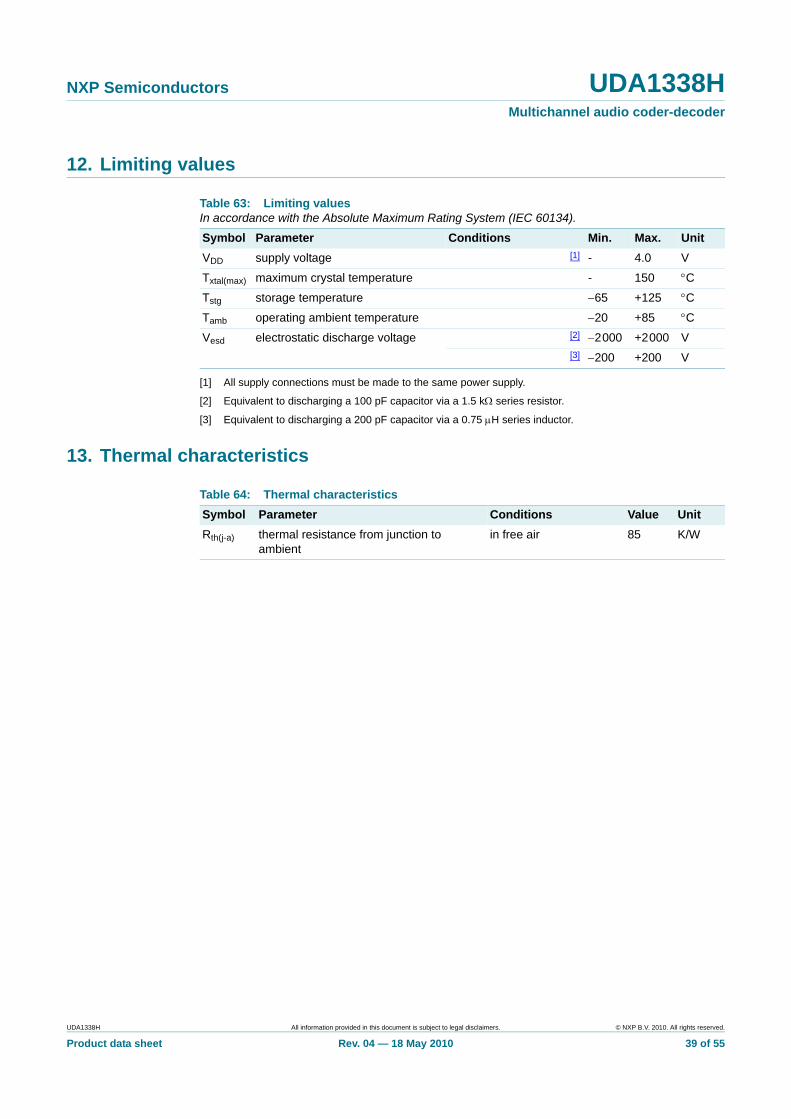
12. Limiting values
[1] All supply connections must be made to the same power supply.
[2] Equivalent to discharging a 100 pF capacitor via a 1.5 kΩ series resistor.
[3] Equivalent to discharging a 200 pF capacitor via a 0.75 μH series inductor.
13. Thermal characteristics
Table 63: Limiting valuesIn accordance with the Absolute Maximum Rating System (IEC 60134).
Symbol Parameter Conditions Min. Max. UnitVDD supply voltage [1] - 4.0 V
Txtal(max) maximum crystal temperature - 150 °C
Tstg storage temperature −65 +125 °C
Tamb operating ambient temperature −20 +85 °C
Vesd electrostatic discharge voltage [2] −2000 +2000 V[3] −200 +200 V
Table 64: Thermal characteristicsSymbol Parameter Conditions Value UnitRth(j-a) thermal resistance from junction to
ambientin free air 85 K/W
UDA1338H All information provided in this document is subject to legal disclaimers. © NXP B.V. 2010. All rights reserved.
Product data sheet Rev. 04 — 18 May 2010 39 of 55

NXP Semiconductors UDA1338HMultichannel audio coder-decoder
14. Static characteristics
Table 65: DC characteristicsVDDD = VDDA(AD) = VDDA(DA) = 3.3 V; Tamb = 25 °C; RL = 22 kΩ; all voltages referenced to ground (pins VSS); unless otherwise specified.
Symbol Parameter Conditions Min. Typ. Max. UnitSuppliesVDDA(AD) ADC analog supply
voltage[1] 2.7 3.3 3.6 V
VDDA(DA) DAC analog supply voltage
[1] 2.7 3.3 3.6 V
VDDD digital supply voltage [1] 2.7 3.3 3.6 V
IDDA(AD) ADC analog supply current
fADC = 48 kHz - 30 - mA
fADC = 96 kHz - 31 - mA
IDDA(DA) DAC analog supply current
fDAC = 48 kHz - 20 - mA
fDAC = 96 kHz - 32 - mA
IDDD digital supply current fADC = fDAC = 48 kHz; fVOICE = 48 kHz
- 31 - mA
fADC = fDAC = 96 kHz; fVOICE = 48 kHz
- 55 - mA
IDDD(pd) digital supply current in Power-down mode
audio and voice ADCs power-down
- 18 - mA
DAC power-down - 14 - mA
Digital input pins (5 V tolerant TTL compatible)VIH HIGH-level input
voltage2.0 - - V
VIL LOW-level input voltage
- - 0.8 V
ILI input leakage current - - 1 μA
Ci input capacitance - - 10 pF
Digital output pinsVOH HIGH-level output
voltageIOH = −2 mA 0.85VDDD - - V
VOL LOW-level output voltage
IOL = 2 mA - - 0.4 V
Analog-to-digital converterVref reference voltage on
pin Vref
with respect to VSSA(AD)
0.45VDDA(AD) 0.5VDDA(AD) 0.55VDDA(AD) V
VADCP positive reference voltage of ADC
- VDDA(AD) - V
VADCN negative reference voltage of ADC
0.0 0.0 0.0 V
Ro output resistance on pin Vref
- 5 - kΩ
Ri(ADC) input resistance of audio ADC
- 10 - kΩ
UDA1338H All information provided in this document is subject to legal disclaimers. © NXP B.V. 2010. All rights reserved.
Product data sheet Rev. 04 — 18 May 2010 40 of 55

NXP Semiconductors UDA1338HMultichannel audio coder-decoder
[1] All supply connections must be made to the same power supply unit.
15. Dynamic characteristics
Ri(VADC) input resistance of voice ADC
- 5 - kΩ
Digital-to-analog converterRL load resistance 4 - - kΩ
Ro output resistance - 1 - kΩ
Table 65: DC characteristics …continuedVDDD = VDDA(AD) = VDDA(DA) = 3.3 V; Tamb = 25 °C; RL = 22 kΩ; all voltages referenced to ground (pins VSS); unless otherwise specified.
Symbol Parameter Conditions Min. Typ. Max. Unit
Table 66: AC characteristicsVDDD = VDDA(AD) = VDDA(DA) = 3.3 V; fi = 1 kHz; Tamb = 25 °C; RL = 22 kΩ; sampling frequency fs = 48 kHz; all voltages referenced to ground (pins VSS); unless otherwise specified.
Symbol Parameter Conditions Min. Typ. Max. UnitAudio analog-to-digital converterD0 digital output level at 0 dB setting; 900 mV
input[1][2] −2.5 −1.2 −0.7 dB
at 3 dB setting; 637 mV input
[2] - −1.2 - dB
at 6 dB setting; 451 mV input
[2] - −1.2 - dB
at 9 dB setting; 319 mV input
[2] - −1.2 - dB
at 12 dB setting; 226 mV input
[2] - −1.2 - dB
at 15 dB setting; 160 mV input
[2] - −1.2 - dB
at 18 dB setting; 113 mV input
[2] - −1.2 - dB
at 21 dB setting; 80 mV input
[2] - −1.2 - dB
at 24 dB setting; 57 mV input
[2] - −1.2 - dB
ΔVi input voltage unbalance between channels
- 0.1 - dB
UDA1338H All information provided in this document is subject to legal disclaimers. © NXP B.V. 2010. All rights reserved.
Product data sheet Rev. 04 — 18 May 2010 41 of 55

NXP Semiconductors UDA1338HMultichannel audio coder-decoder
(THD + N)/S total harmonic distortion-plus-noise to signal ratio
normal mode; at −1 dBFS
at 0 dB setting - −90 −83 dB
at 3 dB setting - −90 - dB
at 6 dB setting - −90 - dB
at 9 dB setting - −90 - dB
at 12 dB setting - −90 - dB
at 15 dB setting - −89 - dB
at 18 dB setting - −87 - dB
at 21 dB setting - −85 - dB
at 24 dB setting - −83 - dB
normal mode; at −60 dBFS; A-weighted
at 0 dB setting - −40 −34 dB
at 3 dB setting - −40 - dB
at 6 dB setting - −40 - dB
at 9 dB setting - −39 - dB
at 12 dB setting - −38 - dB
at 15 dB setting - −37 - dB
at 18 dB setting - −35 - dB
at 21 dB setting - −32 - dB
at 24 dB setting - −30 - dB
S/N signal-to-noise ratio code = 0; A-weighted 94 100 - dB
αcs channel separation - 100 - dB
Voice analog-to-digital converterVi(rms) input voltage (RMS value) at 0 dBFS digital output;
2.2 kΩ source impedance- 50.0 - mV
(THD + N)/S total harmonic distortion-plus-noise to signal ratio
at −1 dBFS - −78 - dB
at −20 dBFS - −65 - dB
at −40 dBFS; A-weighted - −47 - dB
S/N signal-to-noise ratio code = 0; A-weighted - 87 - dB
Digital-to-analog converterDifferential mode
Vo(rms) output voltage (RMS value) at 0 dBFS digital input 1.9 2.0 2.1 V
ΔVo output voltage unbalance between channels
- <0.1 - dB
(THD + N)/S total harmonic distortion-plus-noise to signal ratio
at 0 dBFS - −100 −93 dB
at −20 dBFS - −90 - dB
at −60 dBFS; A-weighted - −50 −45 dB
S/N signal-to-noise ratio code = 0; A-weighted 107 114 - dB
αcs channel separation - 117 - dB
Table 66: AC characteristics …continuedVDDD = VDDA(AD) = VDDA(DA) = 3.3 V; fi = 1 kHz; Tamb = 25 °C; RL = 22 kΩ; sampling frequency fs = 48 kHz; all voltages referenced to ground (pins VSS); unless otherwise specified.
Symbol Parameter Conditions Min. Typ. Max. Unit
UDA1338H All information provided in this document is subject to legal disclaimers. © NXP B.V. 2010. All rights reserved.
Product data sheet Rev. 04 — 18 May 2010 42 of 55
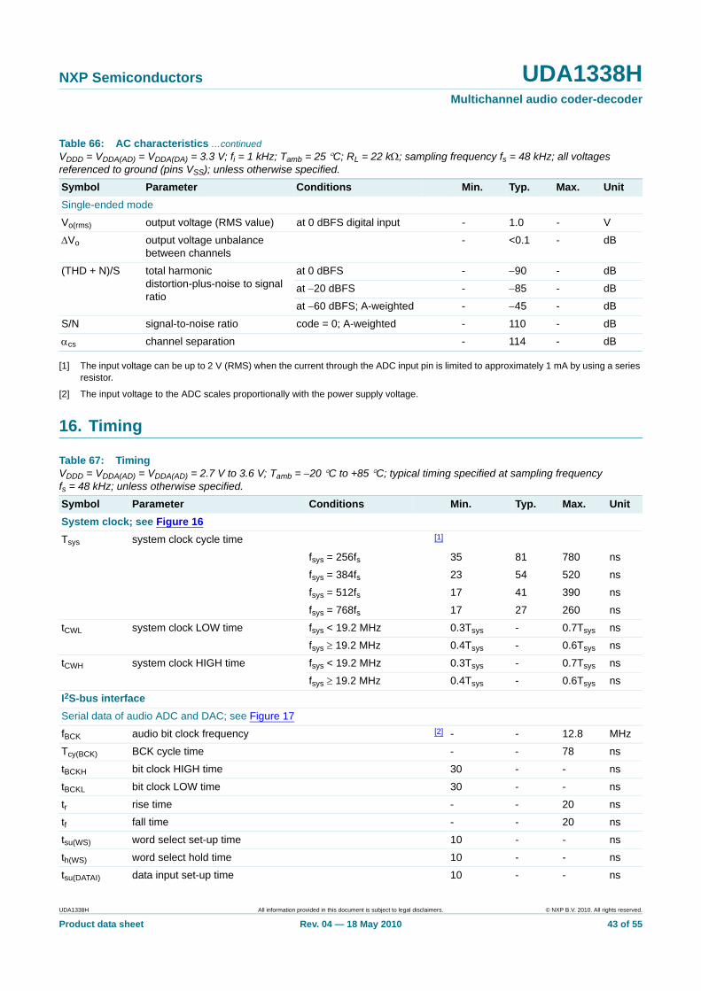
NXP Semiconductors UDA1338HMultichannel audio coder-decoder
[1] The input voltage can be up to 2 V (RMS) when the current through the ADC input pin is limited to approximately 1 mA by using a series resistor.
[2] The input voltage to the ADC scales proportionally with the power supply voltage.
16. Timing
Single-ended mode
Vo(rms) output voltage (RMS value) at 0 dBFS digital input - 1.0 - V
ΔVo output voltage unbalance between channels
- <0.1 - dB
(THD + N)/S total harmonic distortion-plus-noise to signal ratio
at 0 dBFS - −90 - dB
at −20 dBFS - −85 - dB
at −60 dBFS; A-weighted - −45 - dB
S/N signal-to-noise ratio code = 0; A-weighted - 110 - dB
αcs channel separation - 114 - dB
Table 66: AC characteristics …continuedVDDD = VDDA(AD) = VDDA(DA) = 3.3 V; fi = 1 kHz; Tamb = 25 °C; RL = 22 kΩ; sampling frequency fs = 48 kHz; all voltages referenced to ground (pins VSS); unless otherwise specified.
Symbol Parameter Conditions Min. Typ. Max. Unit
Table 67: TimingVDDD = VDDA(AD) = VDDA(AD) = 2.7 V to 3.6 V; Tamb = −20 °C to +85 °C; typical timing specified at sampling frequency fs = 48 kHz; unless otherwise specified.
Symbol Parameter Conditions Min. Typ. Max. UnitSystem clock; see Figure 16Tsys system clock cycle time [1]
fsys = 256fs 35 81 780 ns
fsys = 384fs 23 54 520 ns
fsys = 512fs 17 41 390 ns
fsys = 768fs 17 27 260 ns
tCWL system clock LOW time fsys < 19.2 MHz 0.3Tsys - 0.7Tsys ns
fsys ≥ 19.2 MHz 0.4Tsys - 0.6Tsys ns
tCWH system clock HIGH time fsys < 19.2 MHz 0.3Tsys - 0.7Tsys ns
fsys ≥ 19.2 MHz 0.4Tsys - 0.6Tsys ns
I2S-bus interfaceSerial data of audio ADC and DAC; see Figure 17
fBCK audio bit clock frequency [2] - - 12.8 MHz
Tcy(BCK) BCK cycle time - - 78 ns
tBCKH bit clock HIGH time 30 - - ns
tBCKL bit clock LOW time 30 - - ns
tr rise time - - 20 ns
tf fall time - - 20 ns
tsu(WS) word select set-up time 10 - - ns
th(WS) word select hold time 10 - - ns
tsu(DATAI) data input set-up time 10 - - ns
UDA1338H All information provided in this document is subject to legal disclaimers. © NXP B.V. 2010. All rights reserved.
Product data sheet Rev. 04 — 18 May 2010 43 of 55

NXP Semiconductors UDA1338HMultichannel audio coder-decoder
th(DATAI) data input hold time 10 - - ns
th(DATAO) data output hold time 0 - - ns
td(DATAO-BCK) data output to bit clock delay - - 30 ns
td(DATAO-WS) data output to word select delay - - 30 ns
Serial data of voice ADC
fBCKV voice bit clock frequency [2] - - 6.4 MHz
Tcy(BCKV) BCKV cycle time - - 156 ns
tBCKVH bit clock HIGH time 50 - - ns
tBCKVL bit clock LOW time 50 - - ns
tr rise time - - 20 ns
tf fall time - - 20 ns
tsu(WSV) word select set-up time 10 - - ns
th(WSV) word select hold time 10 - - ns
th(DATAV) data output hold time 0 - - ns
td(DATAV-BCKV) data output to bit clock delay - - 30 ns
td(DATAV-WSV) data output to word select delay - - 30 ns
td(WSV-BCKV) word select to bit clock delay WSV-out mode −30 - +30 ns
L3-bus interface; see Figure 18 and 19L3CLOCK timing
fcy(CLK)L3 L3CLK frequency - - 2000 kHz
Tcy(CLK)L3 L3CLOCK cycle time 500 - - ns
tCLK(L3)H L3CLOCK HIGH time 250 - - ns
tCLK(L3)L L3CLOCK LOW time 250 - - ns
L3MODE timing
tsu(L3)A L3MODE set-up time in address mode
190 - - ns
th(L3)A L3MODE hold time in address mode 190 - - ns
tsu(L3)D L3MODE set-up time in data transfer mode
190 - - ns
th(L3)D L3MODE hold time in data transfer mode
190 - - ns
tstp(L3) L3MODE stop time in data transfer mode
190 - - ns
L3DATA timing
tsu(L3)DA L3DATA set-up time in data transfer and address mode
190 - - ns
th(L3)DA L3DATA hold time in data transfer and address mode
30 - - ns
td(L3)R L3DATA delay time for read data 0 - 50 ns
tdis(L3)R L3DATA disable time for read data 0 - 50 ns
Table 67: Timing …continuedVDDD = VDDA(AD) = VDDA(AD) = 2.7 V to 3.6 V; Tamb = −20 °C to +85 °C; typical timing specified at sampling frequency fs = 48 kHz; unless otherwise specified.
Symbol Parameter Conditions Min. Typ. Max. Unit
UDA1338H All information provided in this document is subject to legal disclaimers. © NXP B.V. 2010. All rights reserved.
Product data sheet Rev. 04 — 18 May 2010 44 of 55

NXP Semiconductors UDA1338HMultichannel audio coder-decoder
[1] The system clock should not exceed 58 MHz in any mode.
[2] The bit clock frequency should not exceed 256 times the corresponding sampling frequency.
[3] Cb is the total capacitance for each bus line.
[4] To be suppressed by the input filter.
I2C-bus interface timing; see Figure 20SCL timing
fSCL SCL clock frequency 0 - 400 kHz
tLOW SCL LOW time 1.3 - - μs
tHIGH SCL HIGH time 0.6 - - μs
tr rise time SDA and SCL [3] 20 + 0.1Cb - 300 ns
tf fall time SDA and SCL [3] 20 + 0.1Cb - 300 ns
SDA timing
tBUF bus free time between STOP and START condition
1.3 - - μs
tSU;STA set-up time repeated START 0.6 - - μs
tHD;STA hold time START condition 0.6 - - μs
tSU;DAT data set-up time 100 - - ns
tHD;DAT data hold time 0 - - μs
tSU;STO set-up time STOP condition 0.6 - - μs
tSP pulse width of spikes [4] 0 - 50 ns
Cb capacitive load for each bus line - - 400 pF
Table 67: Timing …continuedVDDD = VDDA(AD) = VDDA(AD) = 2.7 V to 3.6 V; Tamb = −20 °C to +85 °C; typical timing specified at sampling frequency fs = 48 kHz; unless otherwise specified.
Symbol Parameter Conditions Min. Typ. Max. Unit
Fig 16. System clock timing
mgr984
Tsys
tCWH
tCWL
UDA1338H All information provided in this document is subject to legal disclaimers. © NXP B.V. 2010. All rights reserved.
Product data sheet Rev. 04 — 18 May 2010 45 of 55

NXP Semiconductors UDA1338HMultichannel audio coder-decoder
Fig 17. I2S-bus serial interface timing
mgs756
WS
BCK
DATAO
DATAI
tftr th(WS)
tsu(WS)
tBCKH
tBCKL
Tcy(BCK)th(DATAO)
tsu(DATAI)th(DATAI)
td(DATAO-BCK)
td(DATAO-WS)
Fig 18. L3-bus address mode timing
th(L3)A
th(L3)DAtsu(L3)DA
Tcy(CLK)(L3)
BIT 0
L3MODE
L3CLOCK
L3DATA BIT 7
mgl723
tCLK(L3)H
tCLK(L3)L
tsu(L3)A
tsu(L3)A
th(L3)A
UDA1338H All information provided in this document is subject to legal disclaimers. © NXP B.V. 2010. All rights reserved.
Product data sheet Rev. 04 — 18 May 2010 46 of 55

NXP Semiconductors UDA1338HMultichannel audio coder-decoder
Fig 19. L3-bus data transfer (write and read) mode timing
tstp(L3)
tsu(L3)D
th(L3)DA
ten(L3)Rth(L3)R
tsu(L3)DA
th(L3)DTcy(CLK)L3
BIT 0
L3MODE
L3CLOCK
L3DATAread
L3DATAwrite
BIT 7
mgu015
tCLK(L3)H
tCLK(L3)L
tsu(L3)R tdis(L3)R
Fig 20. I2C-bus timing
msc610
S SrtSU;STOtSU;STAtHD;STA tHIGH
tLOW tSU;DAT
tHD;DAT
tf
SDA
SCL
P S
tBUFtrtftr tSPtHD;STA
UDA1338H All information provided in this document is subject to legal disclaimers. © NXP B.V. 2010. All rights reserved.
Product data sheet Rev. 04 — 18 May 2010 47 of 55

NXP Semiconductors UDA1338HMultichannel audio coder-decoder
17. Package outline
Fig 21. Package outline SOT307-2 (QFP44)
UNIT A1 A2 A3 bp c E(1) e HE L Lp Zywv θ
REFERENCESOUTLINEVERSION
EUROPEANPROJECTION ISSUE DATE
IEC JEDEC JEITA
mm 0.250.05
1.851.65
0.250.40.2
0.250.14
10.19.9
0.8 1.312.912.3
1.20.8
100
o
o0.15 0.10.15
DIMENSIONS (mm are the original dimensions)
Note
1. Plastic or metal protrusions of 0.25 mm maximum per side are not included.
0.950.55
SOT307-297-08-0103-02-25
D(1) (1)(1)
10.19.9
HD
12.912.3
EZ
1.20.8
D
e
E
B
11
c
EH
D
ZD
A
ZE
e
v M A
X
1
44
34
33 23
22
12
y
θ
A1A
Lp
detail X
L
(A )3A2
pin 1 index
DH v M B
bp
bp
w M
w M
0 2.5 5 mm
scale
QFP44: plastic quad flat package; 44 leads (lead length 1.3 mm); body 10 x 10 x 1.75 mm SOT307-2
Amax.
2.1
UDA1338H All information provided in this document is subject to legal disclaimers. © NXP B.V. 2010. All rights reserved.
Product data sheet Rev. 04 — 18 May 2010 48 of 55

NXP Semiconductors UDA1338HMultichannel audio coder-decoder
18. Handling information
All input and output pins are protected against ElectroStatic Discharge (ESD) under normal handling. When handling ensure that the appropriate precautions are taken as described in JESD625-A or equivalent standards.
19. Soldering of SMD packages
This text provides a very brief insight into a complex technology. A more in-depth account of soldering ICs can be found in Application Note AN10365 “Surface mount reflow soldering description”.
19.1 Introduction to solderingSoldering is one of the most common methods through which packages are attached to Printed Circuit Boards (PCBs), to form electrical circuits. The soldered joint provides both the mechanical and the electrical connection. There is no single soldering method that is ideal for all IC packages. Wave soldering is often preferred when through-hole and Surface Mount Devices (SMDs) are mixed on one printed wiring board; however, it is not suitable for fine pitch SMDs. Reflow soldering is ideal for the small pitches and high densities that come with increased miniaturization.
19.2 Wave and reflow solderingWave soldering is a joining technology in which the joints are made by solder coming from a standing wave of liquid solder. The wave soldering process is suitable for the following:
• Through-hole components• Leaded or leadless SMDs, which are glued to the surface of the printed circuit board
Not all SMDs can be wave soldered. Packages with solder balls, and some leadless packages which have solder lands underneath the body, cannot be wave soldered. Also, leaded SMDs with leads having a pitch smaller than ~0.6 mm cannot be wave soldered, due to an increased probability of bridging.
The reflow soldering process involves applying solder paste to a board, followed by component placement and exposure to a temperature profile. Leaded packages, packages with solder balls, and leadless packages are all reflow solderable.
Key characteristics in both wave and reflow soldering are:
• Board specifications, including the board finish, solder masks and vias• Package footprints, including solder thieves and orientation• The moisture sensitivity level of the packages• Package placement• Inspection and repair• Lead-free soldering versus SnPb soldering
19.3 Wave solderingKey characteristics in wave soldering are:
UDA1338H All information provided in this document is subject to legal disclaimers. © NXP B.V. 2010. All rights reserved.
Product data sheet Rev. 04 — 18 May 2010 49 of 55

NXP Semiconductors UDA1338HMultichannel audio coder-decoder
• Process issues, such as application of adhesive and flux, clinching of leads, board transport, the solder wave parameters, and the time during which components are exposed to the wave
• Solder bath specifications, including temperature and impurities
19.4 Reflow solderingKey characteristics in reflow soldering are:
• Lead-free versus SnPb soldering; note that a lead-free reflow process usually leads to higher minimum peak temperatures (see Figure 22) than a SnPb process, thus reducing the process window
• Solder paste printing issues including smearing, release, and adjusting the process window for a mix of large and small components on one board
• Reflow temperature profile; this profile includes preheat, reflow (in which the board is heated to the peak temperature) and cooling down. It is imperative that the peak temperature is high enough for the solder to make reliable solder joints (a solder paste characteristic). In addition, the peak temperature must be low enough that the packages and/or boards are not damaged. The peak temperature of the package depends on package thickness and volume and is classified in accordance with Table 68 and 69
Moisture sensitivity precautions, as indicated on the packing, must be respected at all times.
Studies have shown that small packages reach higher temperatures during reflow soldering, see Figure 22.
Table 68. SnPb eutectic process (from J-STD-020C)Package thickness (mm) Package reflow temperature (°C)
Volume (mm3)< 350 ≥ 350
< 2.5 235 220
≥ 2.5 220 220
Table 69. Lead-free process (from J-STD-020C)Package thickness (mm) Package reflow temperature (°C)
Volume (mm3)< 350 350 to 2000 > 2000
< 1.6 260 260 260
1.6 to 2.5 260 250 245
> 2.5 250 245 245
UDA1338H All information provided in this document is subject to legal disclaimers. © NXP B.V. 2010. All rights reserved.
Product data sheet Rev. 04 — 18 May 2010 50 of 55
NXP Semiconductors UDA1338HMultichannel audio coder-decoder
For further information on temperature profiles, refer to Application Note AN10365 “Surface mount reflow soldering description”.
MSL: Moisture Sensitivity Level
Fig 22. Temperature profiles for large and small components
001aac844
temperature
time
minimum peak temperature= minimum soldering temperature
maximum peak temperature= MSL limit, damage level
peak temperature
UDA1338H All information provided in this document is subject to legal disclaimers. © NXP B.V. 2010. All rights reserved.
Product data sheet Rev. 04 — 18 May 2010 51 of 55

NXP Semiconductors UDA1338HMultichannel audio coder-decoder
20. Revision history
Table 70: Revision historyDocument ID Release date Data sheet status Change notice Doc. number SupersedesUDA1338H v.4 20100518 Product data sheet - - UDA1338H_3
Modifications: • The format of this data sheet has been redesigned to comply with the new identity guidelines of NXP Semiconductors.
• Legal texts have been adapted to the new company name where appropriate. • Section “Test information” and subsection “Quality information” removed.• Section 18 “Handling information”: text updated• Section 19 “Soldering of SMD packages”: title changed, text updated
UDA1338H_3 20050216 Product data sheet - 9397 750 14389 UDA1338H_2
UDA1338H_2 021121 Preliminary specification
- 9397 750 10089 UDA1338H_1
UDA1338H_1 020523 Preliminary specification
- 9397 750 09319 -
UDA1338H All information provided in this document is subject to legal disclaimers. © NXP B.V. 2010. All rights reserved.
Product data sheet Rev. 04 — 18 May 2010 52 of 55

NXP Semiconductors UDA1338HMultichannel audio coder-decoder
21. Legal information
21.1 Data sheet status
[1] Please consult the most recently issued document before initiating or completing a design.
[2] The term ‘short data sheet’ is explained in section “Definitions”.
[3] The product status of device(s) described in this document may have changed since this document was published and may differ in case of multiple devices. The latest product status information is available on the Internet at URL http://www.nxp.com.
21.2 DefinitionsDraft — The document is a draft version only. The content is still under internal review and subject to formal approval, which may result in modifications or additions. NXP Semiconductors does not give any representations or warranties as to the accuracy or completeness of information included herein and shall have no liability for the consequences of use of such information.
Short data sheet — A short data sheet is an extract from a full data sheet with the same product type number(s) and title. A short data sheet is intended for quick reference only and should not be relied upon to contain detailed and full information. For detailed and full information see the relevant full data sheet, which is available on request via the local NXP Semiconductors sales office. In case of any inconsistency or conflict with the short data sheet, the full data sheet shall prevail.
Product specification — The information and data provided in a Product data sheet shall define the specification of the product as agreed between NXP Semiconductors and its customer, unless NXP Semiconductors and customer have explicitly agreed otherwise in writing. In no event however, shall an agreement be valid in which the NXP Semiconductors product is deemed to offer functions and qualities beyond those described in the Product data sheet.
21.3 DisclaimersLimited warranty and liability — Information in this document is believed to be accurate and reliable. However, NXP Semiconductors does not give any representations or warranties, expressed or implied, as to the accuracy or completeness of such information and shall have no liability for the consequences of use of such information.
In no event shall NXP Semiconductors be liable for any indirect, incidental, punitive, special or consequential damages (including - without limitation - lost profits, lost savings, business interruption, costs related to the removal or replacement of any products or rework charges) whether or not such damages are based on tort (including negligence), warranty, breach of contract or any other legal theory.
Notwithstanding any damages that customer might incur for any reason whatsoever, NXP Semiconductors’ aggregate and cumulative liability towards customer for the products described herein shall be limited in accordance with the Terms and conditions of commercial sale of NXP Semiconductors.
Right to make changes — NXP Semiconductors reserves the right to make changes to information published in this document, including without limitation specifications and product descriptions, at any time and without notice. This document supersedes and replaces all information supplied prior to the publication hereof.
Suitability for use — NXP Semiconductors products are not designed, authorized or warranted to be suitable for use in life support, life-critical or safety-critical systems or equipment, nor in applications where failure or
malfunction of an NXP Semiconductors product can reasonably be expected to result in personal injury, death or severe property or environmental damage. NXP Semiconductors accepts no liability for inclusion and/or use of NXP Semiconductors products in such equipment or applications and therefore such inclusion and/or use is at the customer’s own risk.
Applications — Applications that are described herein for any of these products are for illustrative purposes only. NXP Semiconductors makes no representation or warranty that such applications will be suitable for the specified use without further testing or modification.
Customers are responsible for the design and operation of their applications and products using NXP Semiconductors products, and NXP Semiconductors accepts no liability for any assistance with applications or customer product design. It is customer’s sole responsibility to determine whether the NXP Semiconductors product is suitable and fit for the customer’s applications and products planned, as well as for the planned application and use of customer’s third party customer(s). Customers should provide appropriate design and operating safeguards to minimize the risks associated with their applications and products.
NXP Semiconductors does not accept any liability related to any default, damage, costs or problem which is based on any weakness or default in the customer’s applications or products, or the application or use by customer’s third party customer(s). Customer is responsible for doing all necessary testing for the customer’s applications and products using NXP Semiconductors products in order to avoid a default of the applications and the products or of the application or use by customer’s third party customer(s). NXP does not accept any liability in this respect.
Limiting values — Stress above one or more limiting values (as defined in the Absolute Maximum Ratings System of IEC 60134) will cause permanent damage to the device. Limiting values are stress ratings only and (proper) operation of the device at these or any other conditions above those given in the Recommended operating conditions section (if present) or the Characteristics sections of this document is not warranted. Constant or repeated exposure to limiting values will permanently and irreversibly affect the quality and reliability of the device.
Terms and conditions of commercial sale — NXP Semiconductors products are sold subject to the general terms and conditions of commercial sale, as published at http://www.nxp.com/profile/terms, unless otherwise agreed in a valid written individual agreement. In case an individual agreement is concluded only the terms and conditions of the respective agreement shall apply. NXP Semiconductors hereby expressly objects to applying the customer’s general terms and conditions with regard to the purchase of NXP Semiconductors products by customer.
No offer to sell or license — Nothing in this document may be interpreted or construed as an offer to sell products that is open for acceptance or the grant, conveyance or implication of any license under any copyrights, patents or other industrial or intellectual property rights.
Quick reference data — The Quick reference data is an extract of the product data given in the Limiting values and Characteristics sections of this document, and as such is not complete, exhaustive or legally binding.
Document status[1][2] Product status[3] Definition
Objective [short] data sheet Development This document contains data from the objective specification for product development.
Preliminary [short] data sheet Qualification This document contains data from the preliminary specification.
Product [short] data sheet Production This document contains the product specification.
UDA1338H All information provided in this document is subject to legal disclaimers. © NXP B.V. 2010. All rights reserved.
Product data sheet Rev. 04 — 18 May 2010 53 of 55

NXP Semiconductors UDA1338HMultichannel audio coder-decoder
Export control — This document as well as the item(s) described herein may be subject to export control regulations. Export might require a prior authorization from national authorities.
Non-automotive qualified products — Unless this data sheet expressly states that this specific NXP Semiconductors product is automotive qualified, the product is not suitable for automotive use. It is neither qualified nor tested in accordance with automotive testing or application requirements. NXP Semiconductors accepts no liability for inclusion and/or use of non-automotive qualified products in automotive equipment or applications.
In the event that customer uses the product for design-in and use in automotive applications to automotive specifications and standards, customer (a) shall use the product without NXP Semiconductors’ warranty of the
product for such automotive applications, use and specifications, and (b) whenever customer uses the product for automotive applications beyond NXP Semiconductors’ specifications such use shall be solely at customer’s own risk, and (c) customer fully indemnifies NXP Semiconductors for any liability, damages or failed product claims resulting from customer design and use of the product for automotive applications beyond NXP Semiconductors’ standard warranty and NXP Semiconductors’ product specifications.
21.4 TrademarksNotice: All referenced brands, product names, service names and trademarks are the property of their respective owners.
22. Contact information
For more information, please visit: http://www.nxp.comFor sales office addresses, please send an email to: [email protected]
UDA1338H All information provided in this document is subject to legal disclaimers. © NXP B.V. 2010. All rights reserved.
Product data sheet Rev. 04 — 18 May 2010 54 of 55

NXP Semiconductors UDA1338HMultichannel audio coder-decoder
23. Contents
1 General description . . . . . . . . . . . . . . . . . . . . . . 12 Features and benefits . . . . . . . . . . . . . . . . . . . . 12.1 General . . . . . . . . . . . . . . . . . . . . . . . . . . . . . . . 12.2 Multiple format data interface . . . . . . . . . . . . . . 22.3 Digital sound processing. . . . . . . . . . . . . . . . . . 22.4 Advanced audio configuration . . . . . . . . . . . . . 23 Applications . . . . . . . . . . . . . . . . . . . . . . . . . . . . 24 Quick reference data . . . . . . . . . . . . . . . . . . . . . 25 Ordering information. . . . . . . . . . . . . . . . . . . . . 36 Block diagram . . . . . . . . . . . . . . . . . . . . . . . . . . 47 Pinning information. . . . . . . . . . . . . . . . . . . . . . 57.1 Pinning . . . . . . . . . . . . . . . . . . . . . . . . . . . . . . . 57.2 Pin description . . . . . . . . . . . . . . . . . . . . . . . . . 58 Functional description . . . . . . . . . . . . . . . . . . . 78.1 System clock . . . . . . . . . . . . . . . . . . . . . . . . . . 78.2 Audio analog-to-digital converter (audio ADC) . 88.3 Voice analog-to-digital converter (voice ADC) . 88.4 Decimation filter of audio ADC . . . . . . . . . . . . . 88.5 Decimation filter of voice ADC . . . . . . . . . . . . . 98.6 Interpolation filter of DAC . . . . . . . . . . . . . . . . . 98.7 Noise shaper of DAC . . . . . . . . . . . . . . . . . . . . 98.8 Digital mixer . . . . . . . . . . . . . . . . . . . . . . . . . . . 98.9 Audio digital-to-analog converters . . . . . . . . . 108.10 Power-on reset . . . . . . . . . . . . . . . . . . . . . . . . 108.11 Audio digital interface . . . . . . . . . . . . . . . . . . . 118.12 Voice digital interface . . . . . . . . . . . . . . . . . . . 148.13 DSD mode . . . . . . . . . . . . . . . . . . . . . . . . . . . 148.14 Microcontroller interface mode . . . . . . . . . . . . 159 L3-bus interface . . . . . . . . . . . . . . . . . . . . . . . . 159.1 General . . . . . . . . . . . . . . . . . . . . . . . . . . . . . . 159.2 Device addressing . . . . . . . . . . . . . . . . . . . . . 169.3 Register addressing . . . . . . . . . . . . . . . . . . . . 169.4 Data write mode . . . . . . . . . . . . . . . . . . . . . . . 189.5 Data read mode . . . . . . . . . . . . . . . . . . . . . . . 1810 I2C-bus interface . . . . . . . . . . . . . . . . . . . . . . . 1910.1 General . . . . . . . . . . . . . . . . . . . . . . . . . . . . . . 1910.2 Characteristics of the I2C-bus. . . . . . . . . . . . . 1910.3 Bit transfer . . . . . . . . . . . . . . . . . . . . . . . . . . . 1910.4 Byte transfer . . . . . . . . . . . . . . . . . . . . . . . . . . 2010.5 Data transfer . . . . . . . . . . . . . . . . . . . . . . . . . . 2010.6 Start and stop conditions . . . . . . . . . . . . . . . . 2010.7 Acknowledgment . . . . . . . . . . . . . . . . . . . . . . 2010.8 Device address. . . . . . . . . . . . . . . . . . . . . . . . 2110.9 Register address . . . . . . . . . . . . . . . . . . . . . . 2110.10 Write and read data . . . . . . . . . . . . . . . . . . . . 2210.11 Write cycle . . . . . . . . . . . . . . . . . . . . . . . . . . . 22
10.12 Read cycle . . . . . . . . . . . . . . . . . . . . . . . . . . . 2211 Register mapping . . . . . . . . . . . . . . . . . . . . . . 2311.1 Address mapping . . . . . . . . . . . . . . . . . . . . . . 2311.2 Register mapping. . . . . . . . . . . . . . . . . . . . . . 2511.3 System settings . . . . . . . . . . . . . . . . . . . . . . . 2711.4 Audio ADC and DAC subsystem settings . . . 2811.5 Voice ADC system settings . . . . . . . . . . . . . . 3011.6 Status output register (read only) . . . . . . . . . . 3111.7 DAC channel selection. . . . . . . . . . . . . . . . . . 3211.8 DAC features settings . . . . . . . . . . . . . . . . . . 3311.9 DAC channel 1 to channel 6 settings. . . . . . . 3511.10 DAC mixing channel settings . . . . . . . . . . . . . 3511.11 Audio ADC 1 and ADC 2 input amplifier gain
settings. . . . . . . . . . . . . . . . . . . . . . . . . . . . . . 3611.12 Voice ADC gain settings . . . . . . . . . . . . . . . . 3711.13 Supplemental settings 1. . . . . . . . . . . . . . . . . 3711.14 Supplemental settings 2. . . . . . . . . . . . . . . . . 3812 Limiting values . . . . . . . . . . . . . . . . . . . . . . . . 3913 Thermal characteristics . . . . . . . . . . . . . . . . . 3914 Static characteristics . . . . . . . . . . . . . . . . . . . 4015 Dynamic characteristics. . . . . . . . . . . . . . . . . 4116 Timing . . . . . . . . . . . . . . . . . . . . . . . . . . . . . . . 4317 Package outline. . . . . . . . . . . . . . . . . . . . . . . . 4818 Handling information . . . . . . . . . . . . . . . . . . . 4919 Soldering of SMD packages. . . . . . . . . . . . . . 4919.1 Introduction to soldering. . . . . . . . . . . . . . . . . 4919.2 Wave and reflow soldering. . . . . . . . . . . . . . . 4919.3 Wave soldering . . . . . . . . . . . . . . . . . . . . . . . 4919.4 Reflow soldering . . . . . . . . . . . . . . . . . . . . . . 5020 Revision history . . . . . . . . . . . . . . . . . . . . . . . 5221 Legal information . . . . . . . . . . . . . . . . . . . . . . 5321.1 Data sheet status . . . . . . . . . . . . . . . . . . . . . . 5321.2 Definitions . . . . . . . . . . . . . . . . . . . . . . . . . . . 5321.3 Disclaimers . . . . . . . . . . . . . . . . . . . . . . . . . . 5321.4 Trademarks . . . . . . . . . . . . . . . . . . . . . . . . . . 5422 Contact information . . . . . . . . . . . . . . . . . . . . 5423 Contents. . . . . . . . . . . . . . . . . . . . . . . . . . . . . . 55
© NXP B.V. 2010. All rights reserved.For more information, please visit: http://www.nxp.comFor sales office addresses, please send an email to: [email protected]
Date of release: 18 May 2010Document identifier: UDA1338H
Please be aware that important notices concerning this document and the product(s)described herein, have been included in section ‘Legal information’.