1 microelettronica sequential circuits lection 7
TRANSCRIPT

1
MICROELETTRONICA
Sequential circuits
Lection 7
2
Outline
• Floorplanning• Sequencing• Sequencing Element Design• Max and Min-Delay• Clock Skew• Time Borrowing• Two-Phase Clocking
3
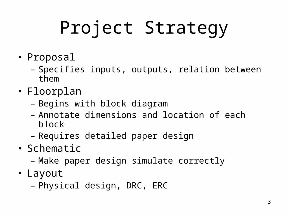
Project Strategy
• Proposal– Specifies inputs, outputs, relation between them
• Floorplan– Begins with block diagram– Annotate dimensions and location of each block– Requires detailed paper design
• Schematic– Make paper design simulate correctly
• Layout– Physical design, DRC, ERC
4
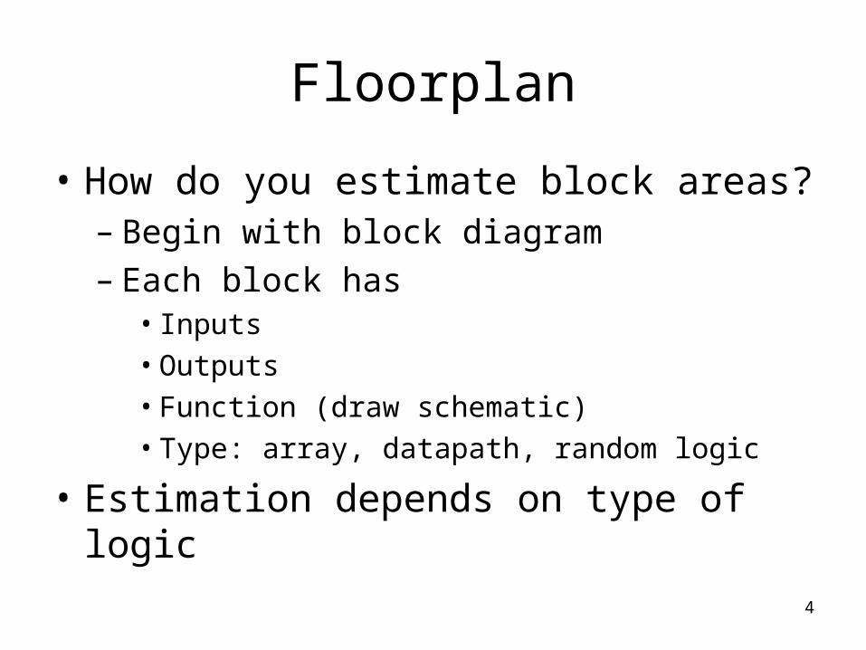
Floorplan
• How do you estimate block areas?– Begin with block diagram– Each block has
• Inputs• Outputs• Function (draw schematic)• Type: array, datapath, random logic
• Estimation depends on type of logic
5
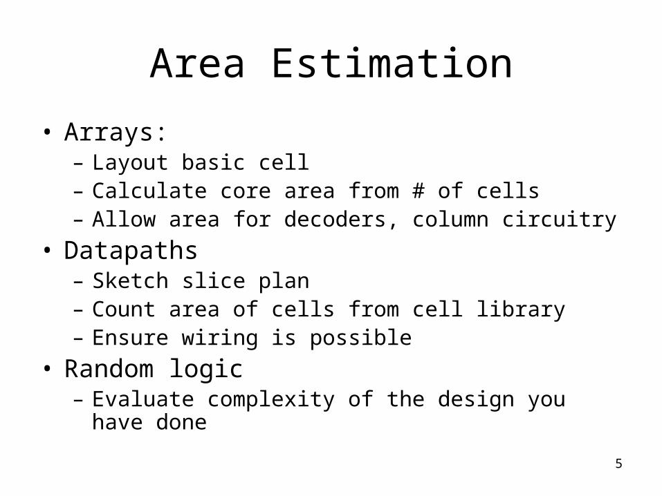
Area Estimation
• Arrays:– Layout basic cell– Calculate core area from # of cells– Allow area for decoders, column circuitry
• Datapaths– Sketch slice plan– Count area of cells from cell library– Ensure wiring is possible
• Random logic– Evaluate complexity of the design you have done
6
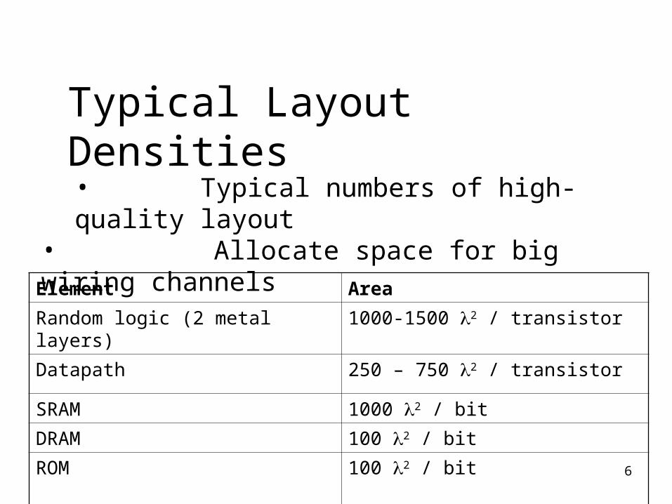
Element Area
Random logic (2 metal layers) 1000-1500 2 / transistor
Datapath 250 – 750 2 / transistor
SRAM 1000 2 / bit
DRAM 100 2 / bit
ROM 100 2 / bit
• Typical numbers of high-quality layout• Allocate space for big wiring channels
Typical Layout Densities
7
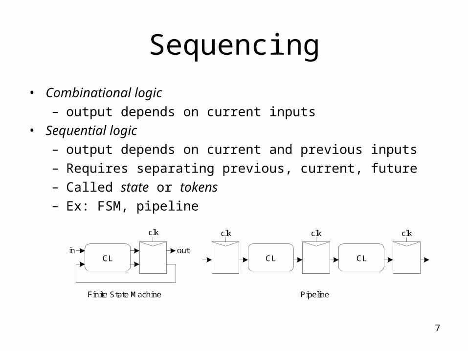
Sequencing
• Combinational logic– output depends on current inputs
• Sequential logic– output depends on current and previous inputs– Requires separating previous, current, future– Called state or tokens– Ex: FSM, pipeline
CL
clk
in out
clk clk clk
CL CL
PipelineFinite State Machine
8
Sequencing Cont.
• If tokens moved through pipeline at constant speed, no sequencing elements would be necessary
• Ex: fiber-optic cable– Light pulses (tokens) are sent down cable– Next pulse sent before first reaches end of cable– No need for hardware to separate pulses– But dispersion sets min time between pulses
• This is called wave pipelining in circuits• In most circuits, dispersion is high
– Delay fast tokens so they don’t catch slow ones.
9
Sequencing Overhead
• Use flip-flops to delay fast tokens so they move through exactly one stage each cycle.
• Inevitably adds some delay to the slow tokens• Makes circuit slower than just the logic delay
– Called sequencing overhead
• Some people call this clocking overhead– But it applies to asynchronous circuits too– Inevitable side effect of maintaining sequence
10
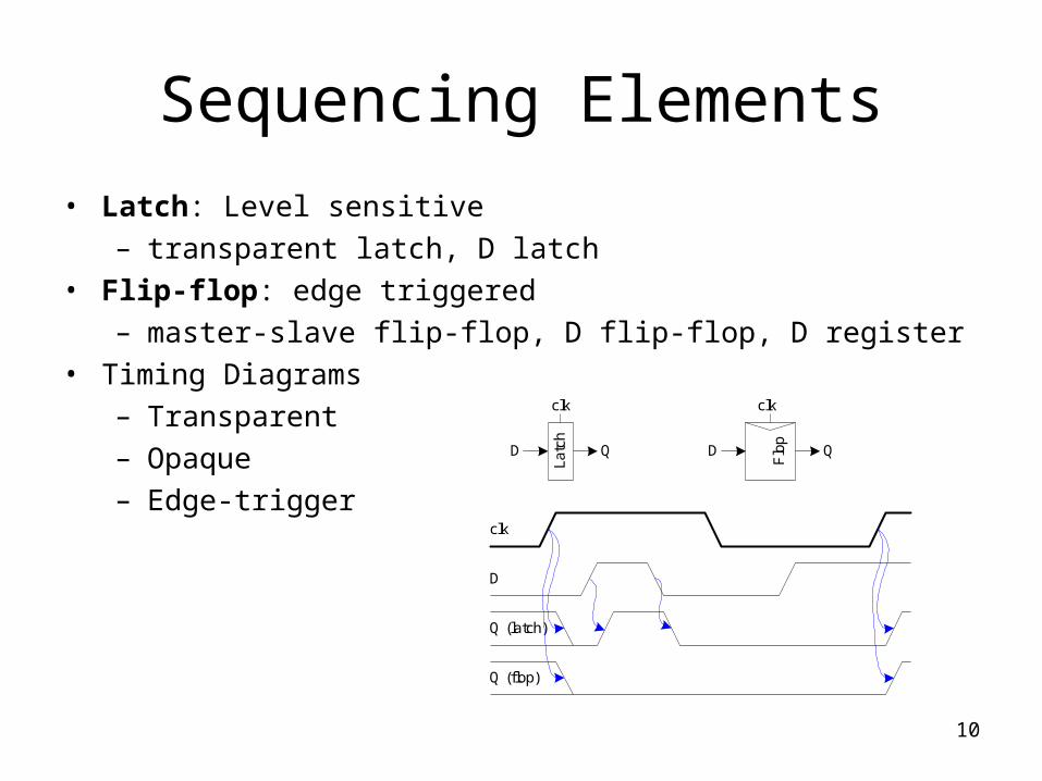
Sequencing Elements
• Latch: Level sensitive– transparent latch, D latch
• Flip-flop: edge triggered– master-slave flip-flop, D flip-flop, D register
• Timing Diagrams– Transparent– Opaque– Edge-trigger
D
Flo
p
Latc
h
Q
clk clk
D Q
clk
D
Q (latch)
Q (flop)
11
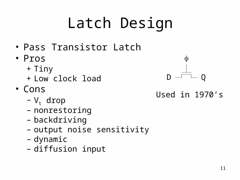
Latch Design
• Pass Transistor Latch• Pros
+ Tiny+ Low clock load
• Cons– Vt drop– nonrestoring– backdriving– output noise sensitivity– dynamic– diffusion input
D Q
Used in 1970’s
12
Latch Design
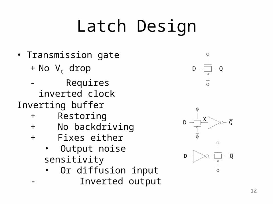
• Transmission gate
+ No Vt drop
- Requires inverted clock
D Q
D
XQ
D Q
Inverting buffer+ Restoring+ No backdriving+ Fixes either
• Output noise sensitivity• Or diffusion input
- Inverted output
13
Latch Design
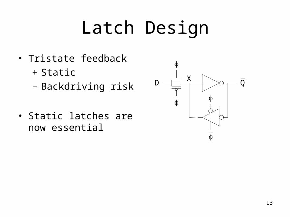
• Tristate feedback
+ Static– Backdriving risk
• Static latches are now essential
QDX

14
Latch Design
• Buffered output+ No backdriving
• Widely used in standard cells+ Very robust (most
important)- Rather large- Rather slow - High clock loading
Q
D X
15
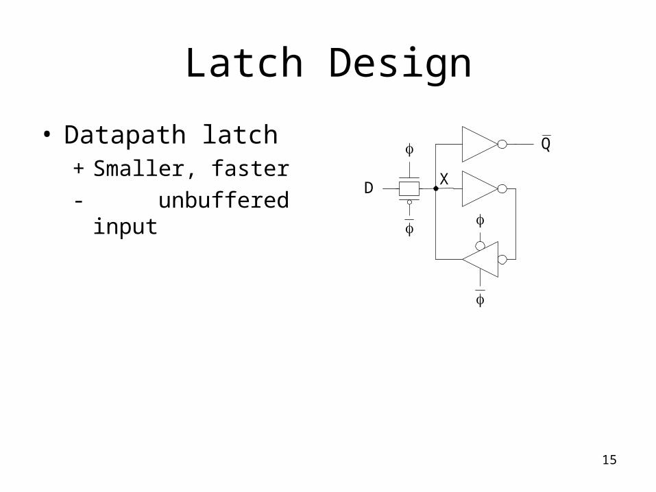
Latch Design
• Datapath latch+ Smaller, faster
- unbuffered input
Q
D X
16
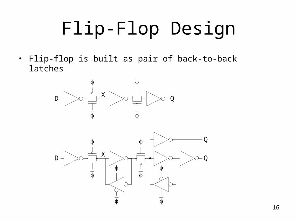
Flip-Flop Design
• Flip-flop is built as pair of back-to-back latches
D Q
X
D
X
Q
Q
17
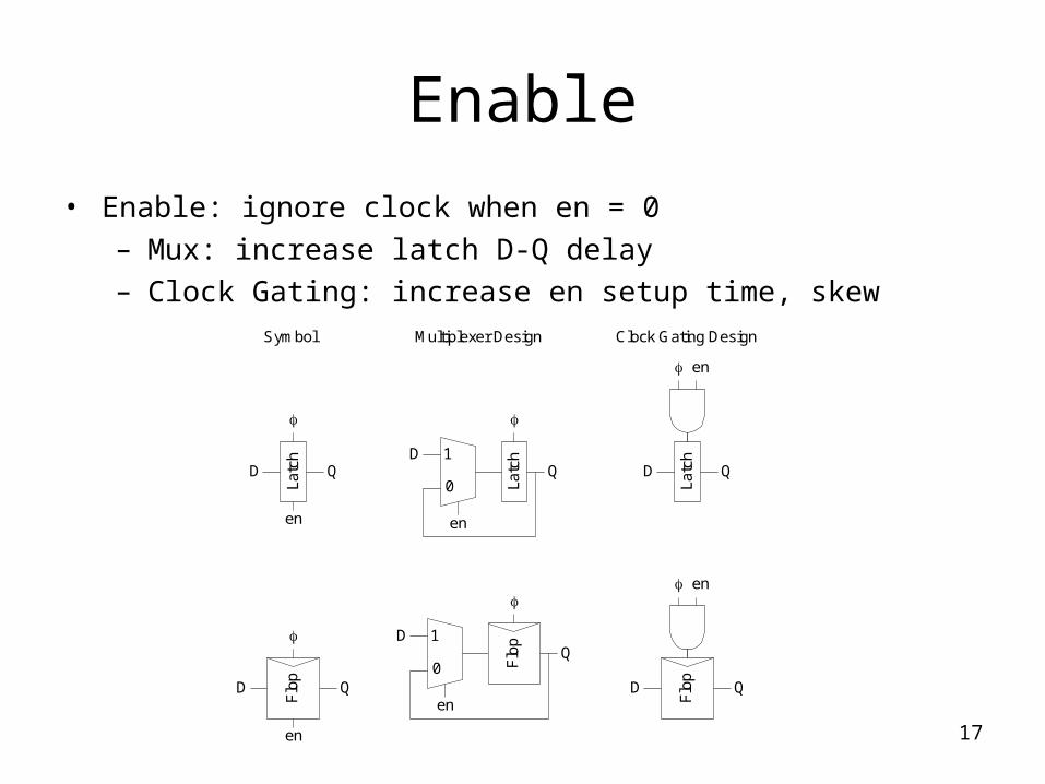
Enable
• Enable: ignore clock when en = 0– Mux: increase latch D-Q delay– Clock Gating: increase en setup time, skew
D Q
Latc
h
D Q
en
en
Latc
hDQ
0
1
en
Latc
h
D Q
en
DQ
0
1
enD Q
en
Flo
p
Flo
p
Flo
p
Symbol Multiplexer Design Clock Gating Design

18
Reset
• Force output low when reset asserted• Synchronous vs. asynchronous
D
Q
Q
reset
D
Q
D
reset
Q
Dreset
reset
reset
Synchronous R
esetA
synchronous Reset
Sym
bol Flo
p
D Q
Latc
h
D Q
reset reset
Q
reset

19
Set / Reset
• Set forces output high when enabled
• Flip-flop with asynchronous set and reset
D
Q
reset
setreset
set
20
Sequencing Methods
• Flip-flops• 2-Phase Latches• Pulsed Latches
Flip-F
lops
Flo
pLa
tch
Flo
p
clk
1
2
p
clk clk
Latc
h
Latc
h
p p
1 12
2-Phase T
ransparent LatchesP
ulsed Latches
Combinational Logic
CombinationalLogic
CombinationalLogic
Combinational Logic
Latc
h
Latc
h
Tc
Tc/2
tnonoverlap tnonoverlap
tpw
Half-Cycle 1 Half-Cycle 1
21
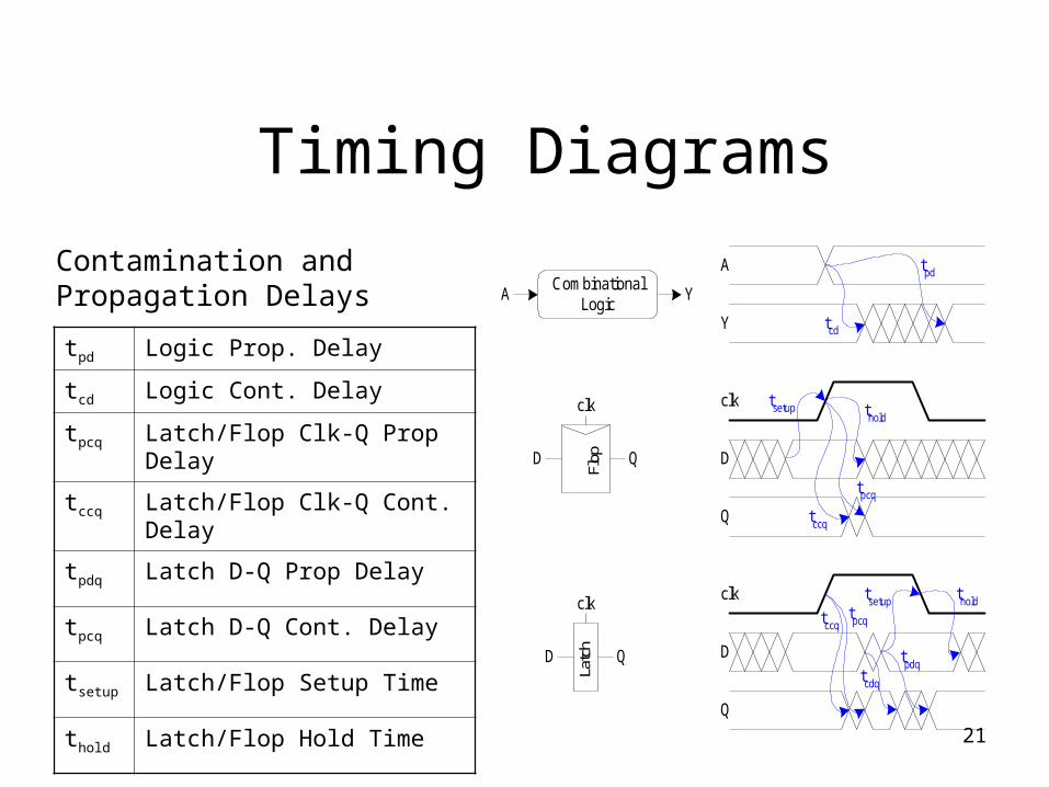
tpd Logic Prop. Delay
tcd Logic Cont. Delay
tpcq Latch/Flop Clk-Q Prop Delay
tccq Latch/Flop Clk-Q Cont. Delay
tpdq Latch D-Q Prop Delay
tpcq Latch D-Q Cont. Delay
tsetup Latch/Flop Setup Time
thold Latch/Flop Hold Time
Contamination and Propagation Delays
Flop
A
Y
tpdCombinational
LogicA Y
D Q
clk clk
D
Q
Latc
h
D Q
clkclk
D
Q
tcd
tsetup thold
tccq
tpcq
tccq
tsetup tholdtpcq
tpdqtcdq
Timing Diagrams
22
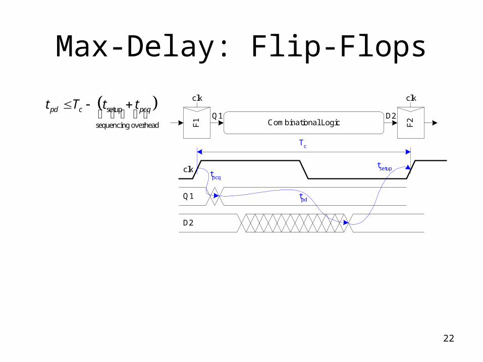
Max-Delay: Flip-Flops
F1
F2
clk
clk clk
Combinational Logic
Tc
Q1 D2
Q1
D2
tpd
tsetuptpcq
setup
sequencing overhead
pd c pcqt T t t
23
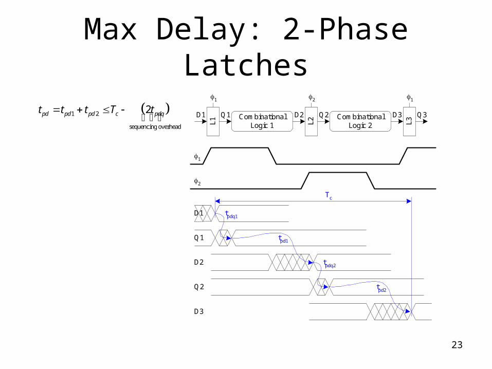
Max Delay: 2-Phase Latches
Tc
Q1
L1
1
2
L2 L3
1 12
CombinationalLogic 1
CombinationalLogic 2
Q2 Q3D1 D2 D3
Q1
D2
Q2
D3
D1
tpd1
tpdq1
tpd2
tpdq2
1 2
sequencing overhead
2pd pd pd c pdqt t t T t
24
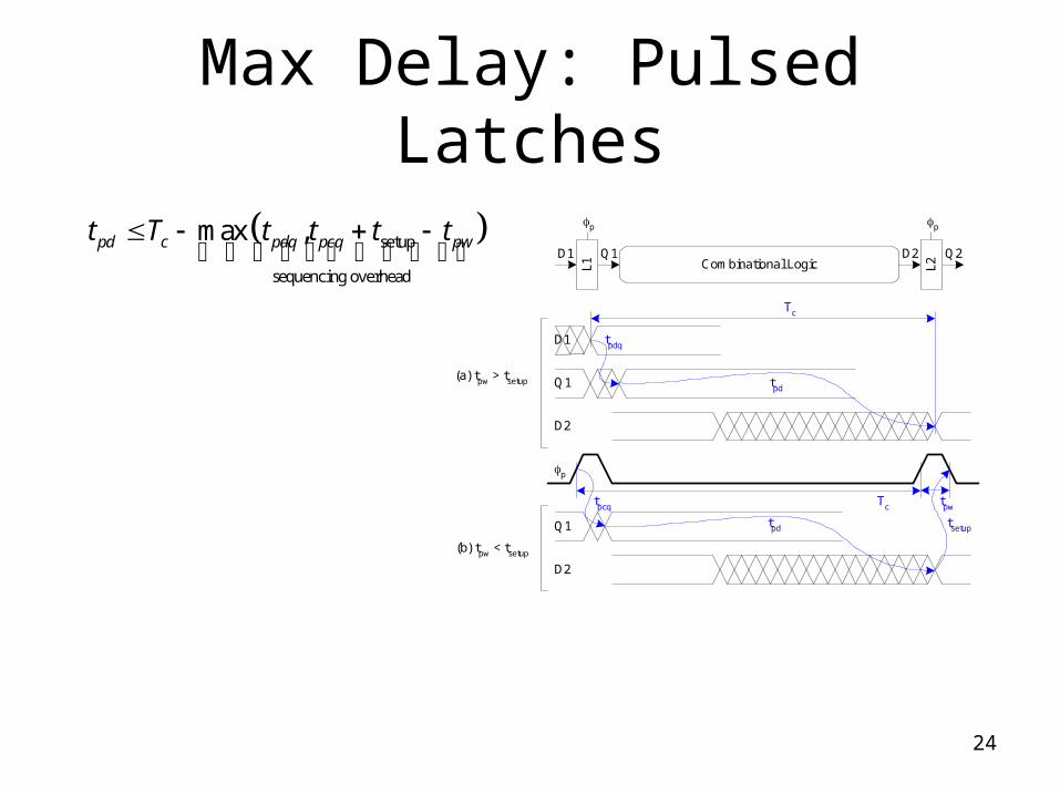
Max Delay: Pulsed Latches
Tc
Q1 Q2D1 D2
Q1
D2
D1
p
p p
Combinational LogicL1 L2
tpw
(a) tpw > tsetup
Q1
D2
(b) tpw < tsetup
Tc
tpd
tpdq
tpcq
tpd tsetup
setup
sequencing overhead
max ,pd c pdq pcq pwt T t t t t
25
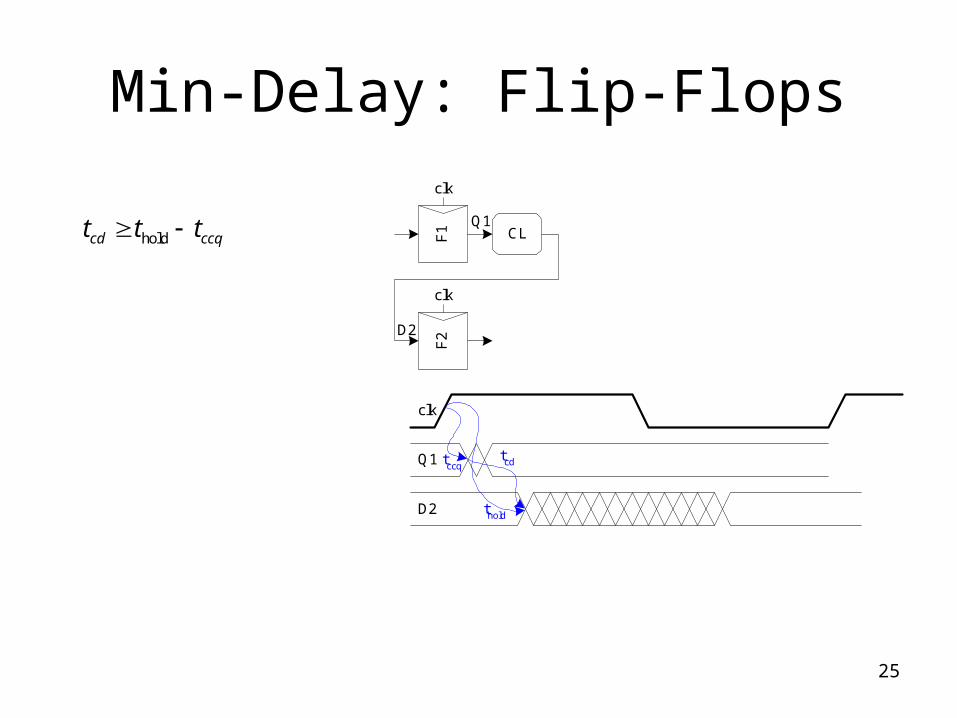
Min-Delay: Flip-Flops
holdcd ccqt t t CL
clk
Q1
D2
F1
clk
Q1
F2
clk
D2
tcd
thold
tccq
26
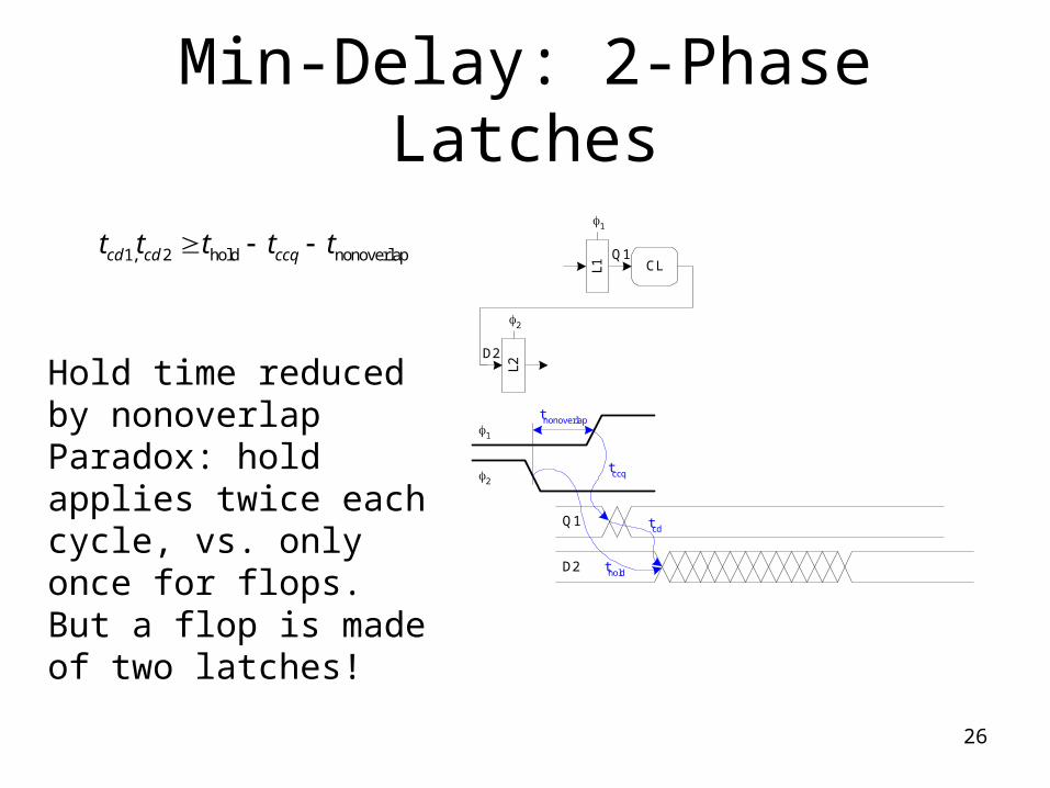
Min-Delay: 2-Phase Latches
1, 2 hold nonoverlapcd cd ccqt t t t t CL
Q1
D2
D2
Q1
1
L1
2
L2
1
2
tnonoverlap
tcd
thold
tccq
Hold time reduced by nonoverlapParadox: hold applies twice each cycle, vs. only once for flops.But a flop is made of two latches!
27
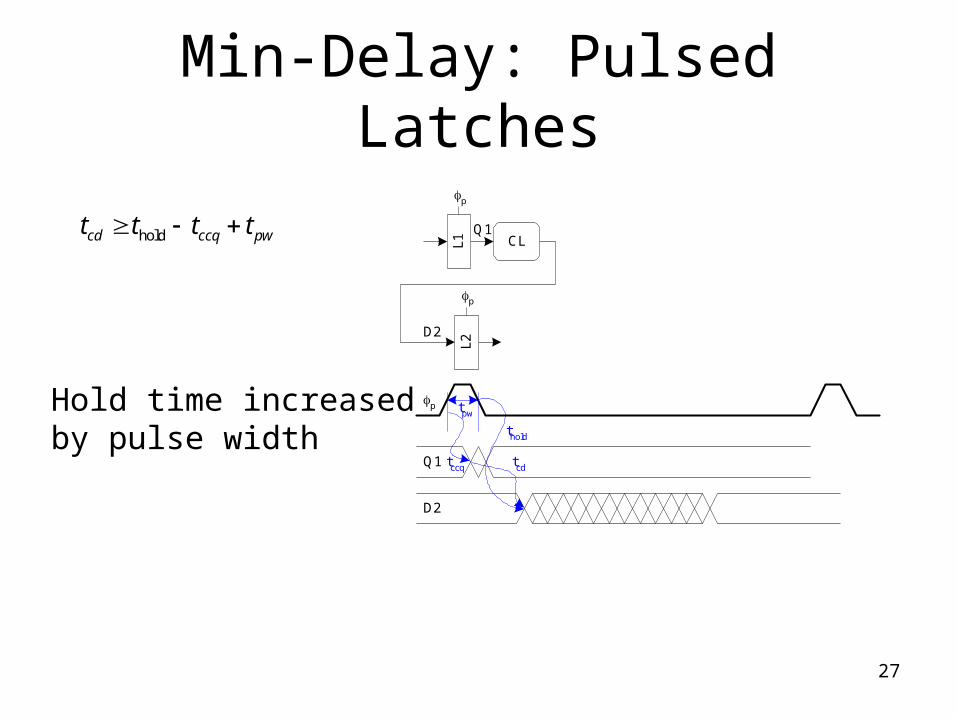
Min-Delay: Pulsed Latches
holdcd ccq pwt t t t CL
Q1
D2
Q1
D2
p tpw
p
L1
p
L2tcd
thold
tccq
Hold time increased by pulse width
28
Time Borrowing
• In a flop-based system:– Data launches on a rising edge– Must setup before next rising edge– If it arrives late, system fails– If it arrives early, time is wasted– Flops have hard edges
• In a latch-based system– Data can pass through latch while transparent– Long cycle of logic can borrow time into next– As long as each loop completes in one cycle

29
Time Borrowing Example
Latc
h
Latc
h
Latc
h
Combinational LogicCombinational
Logic
Borrowing time acrosshalf-cycle boundary
Borrowing time acrosspipeline stage boundary
(a)
(b)
Latc
h
Latc
hCombinational Logic Combinational
Logic
Loops may borrow time internally but must complete within the cycle
1
2
1 1
1
2
2

30
How Much Borrowing?
Q1
L1
1
2
L2
1 2
Combinational Logic 1Q2D1 D2
D2
Tc
Tc/2 Nominal Half-Cycle 1 Delay
tborrow
tnonoverlap
tsetup
borrow setup nonoverlap2cTt t t
borrow setuppwt t t
2-Phase Latches
Pulsed Latches

31
Clock Skew
• We have assumed zero clock skew• Clocks really have uncertainty in arrival time
– Decreases maximum propagation delay– Increases minimum contamination delay– Decreases time borrowing
32
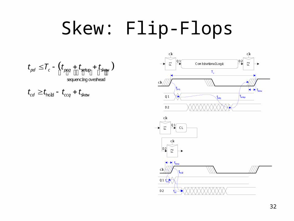
Skew: Flip-Flops
F1
F2
clk
clk clk
Combinational Logic
Tc
Q1 D2
Q1
D2
tskew
CL
Q1
D2
F1
clk
Q1
F2
clk
D2
clk
tskew
tsetup
tpcq
tpdq
tcd
thold
tccq
setup skew
sequencing overhead
hold skew
pd c pcq
cd ccq
t T t t t
t t t t
33
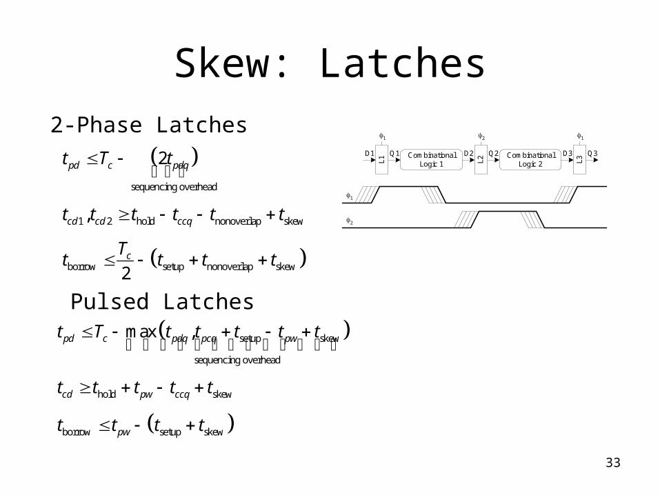
Skew: Latches
Q1
L1
1
2
L2 L3
1 12
CombinationalLogic 1
CombinationalLogic 2
Q2 Q3D1 D2 D3
sequencing overhead
1 2 hold nonoverlap skew
borrow setup nonoverlap skew
2
,
2
pd c pdq
cd cd ccq
c
t T t
t t t t t t
Tt t t t
setup skew
sequencing overhead
hold skew
borrow setup skew
max ,pd c pdq pcq pw
cd pw ccq
pw
t T t t t t t
t t t t t
t t t t
2-Phase Latches
Pulsed Latches
34
Two-Phase Clocking
• If setup times are violated, reduce clock speed• If hold times are violated, chip fails at any speed• An easy way to guarantee hold times is to use 2-
phase latches with big nonoverlap times
• Call these clocks 1, 2 (ph1, ph2)
35
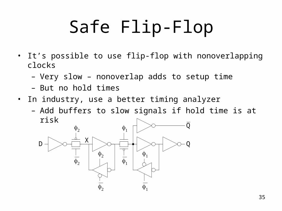
Safe Flip-Flop
• It’s possible to use flip-flop with nonoverlapping clocks– Very slow – nonoverlap adds to setup time– But no hold times
• In industry, use a better timing analyzer– Add buffers to slow signals if hold time is at risk
D
X
Q
Q
36
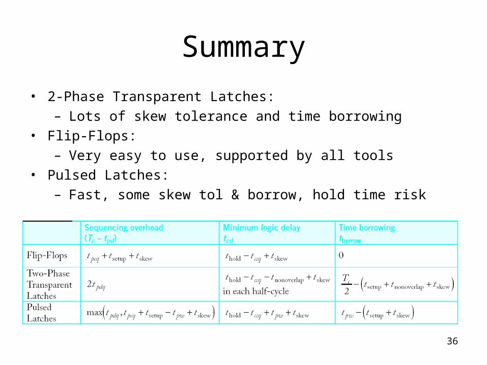
Summary
• 2-Phase Transparent Latches:– Lots of skew tolerance and time borrowing
• Flip-Flops:– Very easy to use, supported by all tools
• Pulsed Latches:– Fast, some skew tol & borrow, hold time risk