1 slides taken from: a.r. hambley, electronics, © prentice hall, 2/e, 2000 a. sedra and k.c. smith,...
TRANSCRIPT
1
Slides taken from:
A.R. Hambley, Electronics, © Prentice Hall, 2/e, 2000
A. Sedra and K.C. Smith, Microelectronic Circuits, © Oxford University Press, 4/e, 1999
Basic Semiconductor Physics
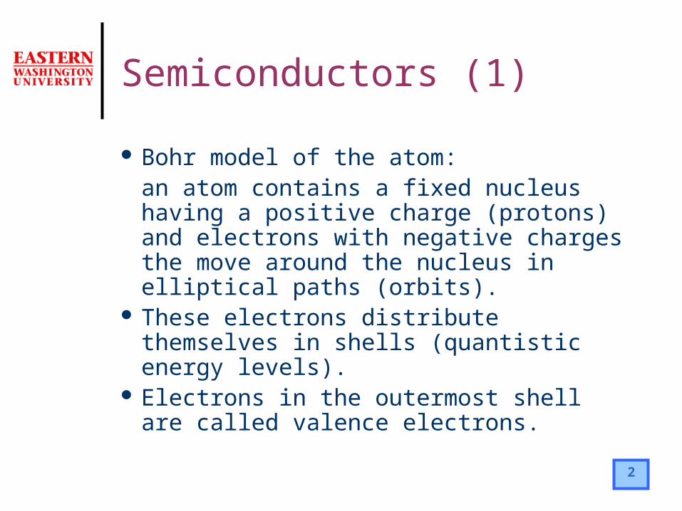
2
Bohr model of the atom:an atom contains a fixed nucleus having a positive charge (protons) and electrons with negative charges the move around the nucleus in elliptical paths (orbits).
These electrons distribute themselves in shells (quantistic energy levels).
Electrons in the outermost shell are called valence electrons.
Semiconductors (1)

3
Semiconductors (2)
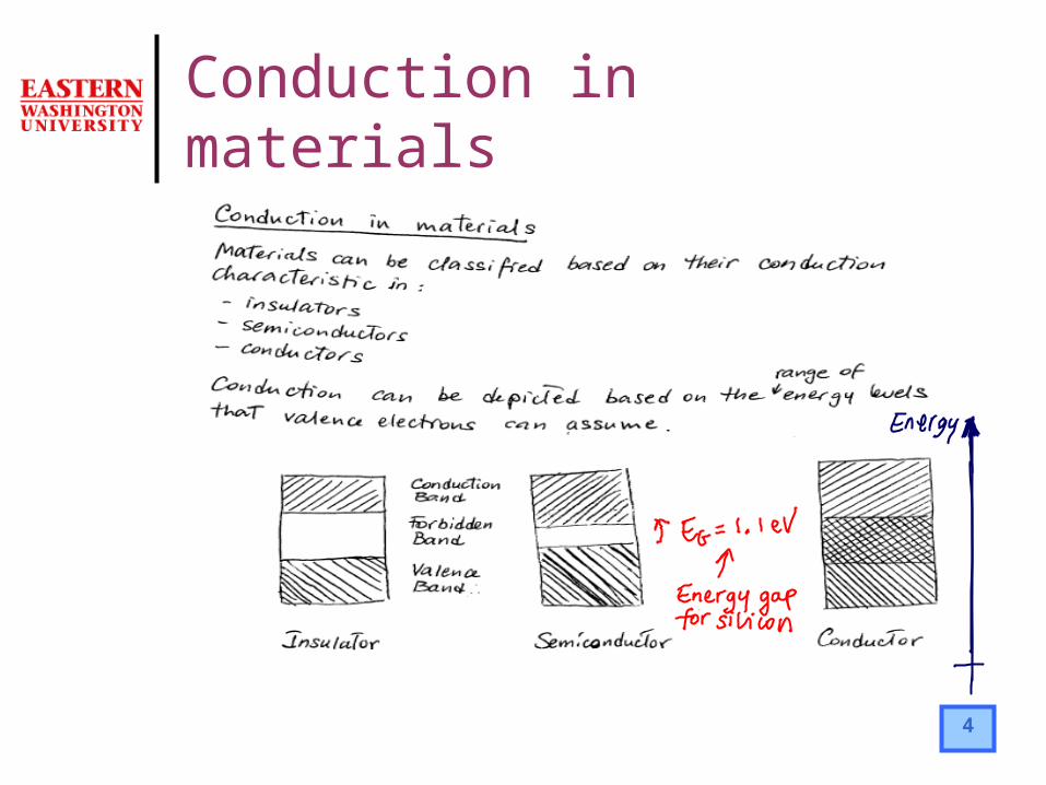
4
Conduction in materials

5Figure 3.36 Intrinsic silicon crystal.
Silicon Intrinsic Crystal
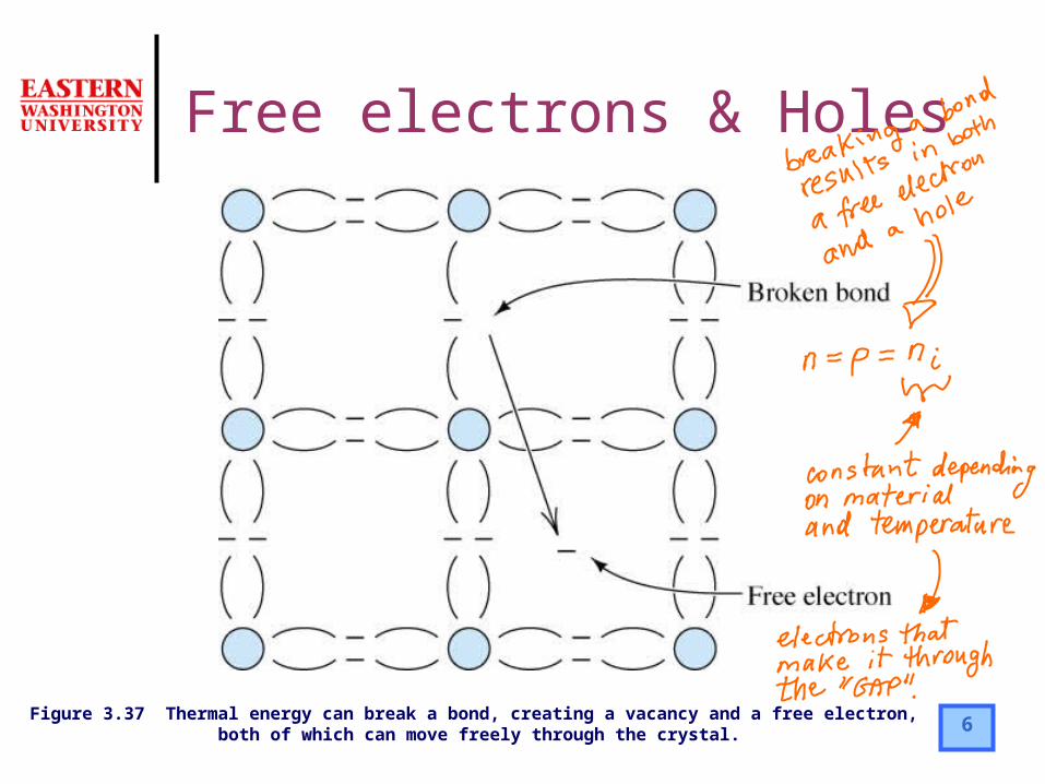
6Figure 3.37 Thermal energy can break a bond, creating a vacancy and a free electron,
both of which can move freely through the crystal.
Free electrons & Holes

7Figure 3.38 As electrons move to the left to fill a hole, the hole moves to the right.
Holes movement

8Figure 3.39 n-type silicon is created by adding valence five impurity atoms.
n-type silicon
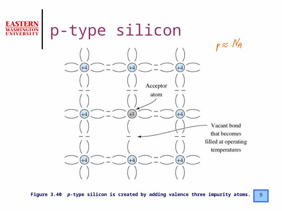
9Figure 3.40 p-type silicon is created by adding valence three impurity atoms.
p-type silicon

10
Figure 3.42 If a pn junction could be formed by joining a p-type crystal to an n-type crystal, a sharp gradient of hole concentration and electron concentration would exist at the junction immediately after joining the crystals.
Constructing a Diode

11Figure 3.43a Diffusion of majority carriers into the opposite sides causes a depletion region to appear at the junction.
Unbiased PN junction

12
Figure 3.43b Diffusion of majority carriers into the opposite sides causes a depletion region to appear at the junction.
Hole concentration across the diode
13
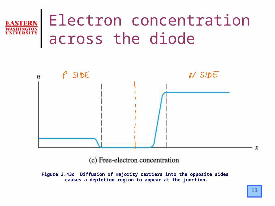
Figure 3.43c Diffusion of majority carriers into the opposite sides causes a depletion region to appear at the junction.
Electron concentration across the diode
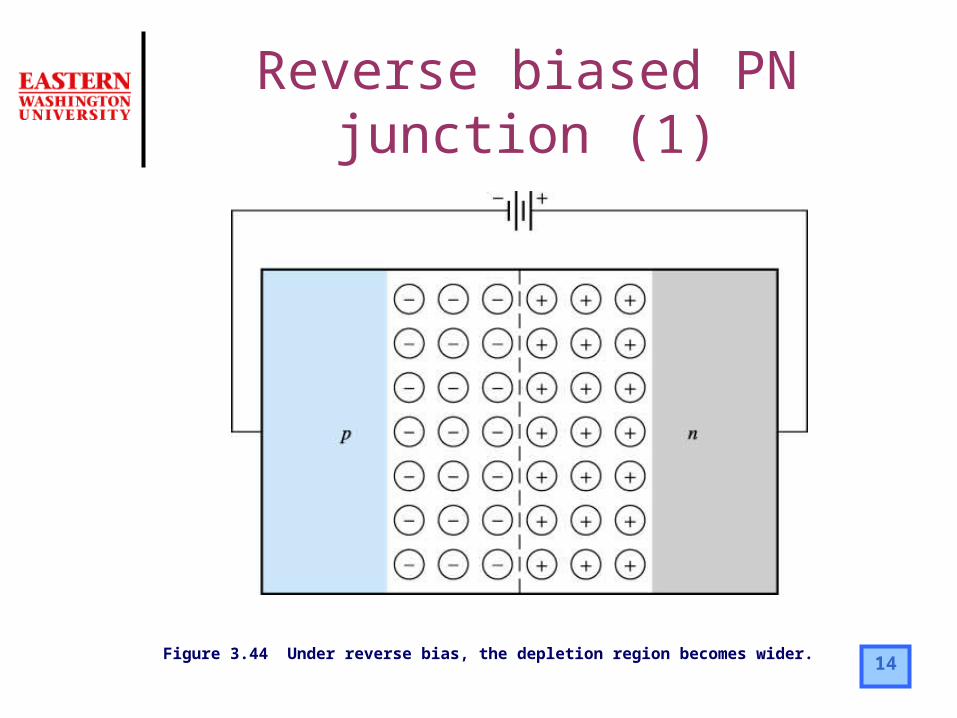
14Figure 3.44 Under reverse bias, the depletion region becomes wider.
Reverse biased PN junction (1)
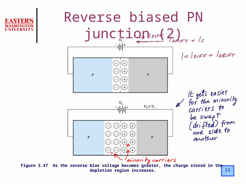
15Figure 3.47 As the reverse bias voltage becomes greater, the charge stored in the
depletion region increases.
Reverse biased PN junction (2)

16Figure 3.46 Parallel-plate capacitor.
PN junction capacitance = Depletion Capacitance
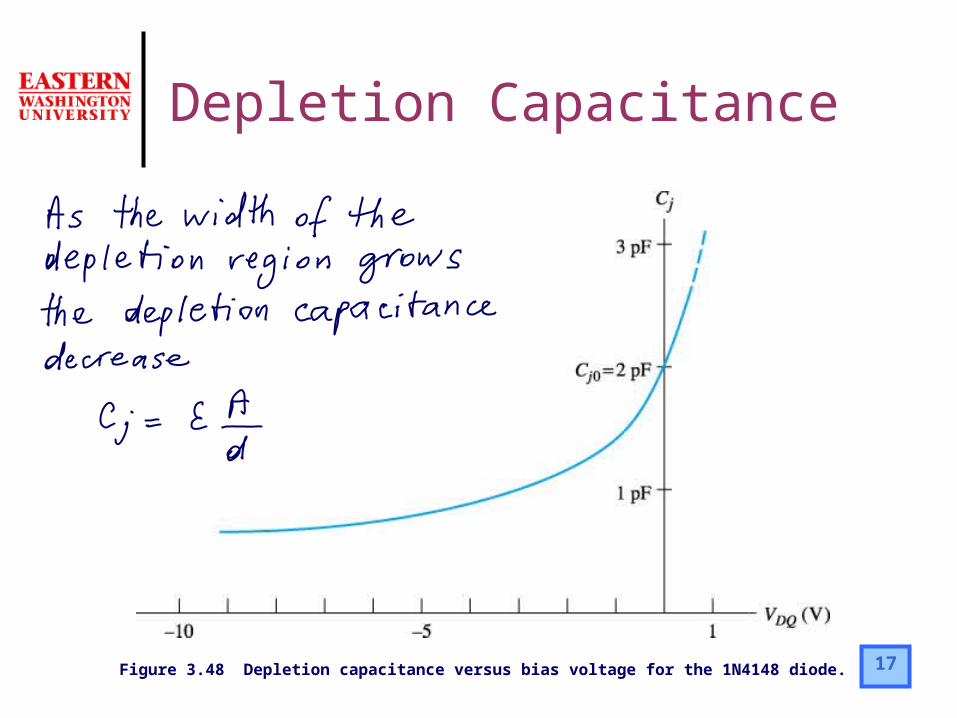
17Figure 3.48 Depletion capacitance versus bias voltage for the 1N4148 diode.
Depletion Capacitance
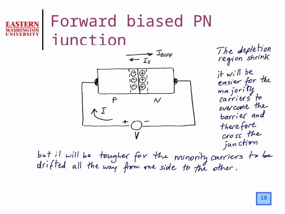
18
Forward biased PN junction
19
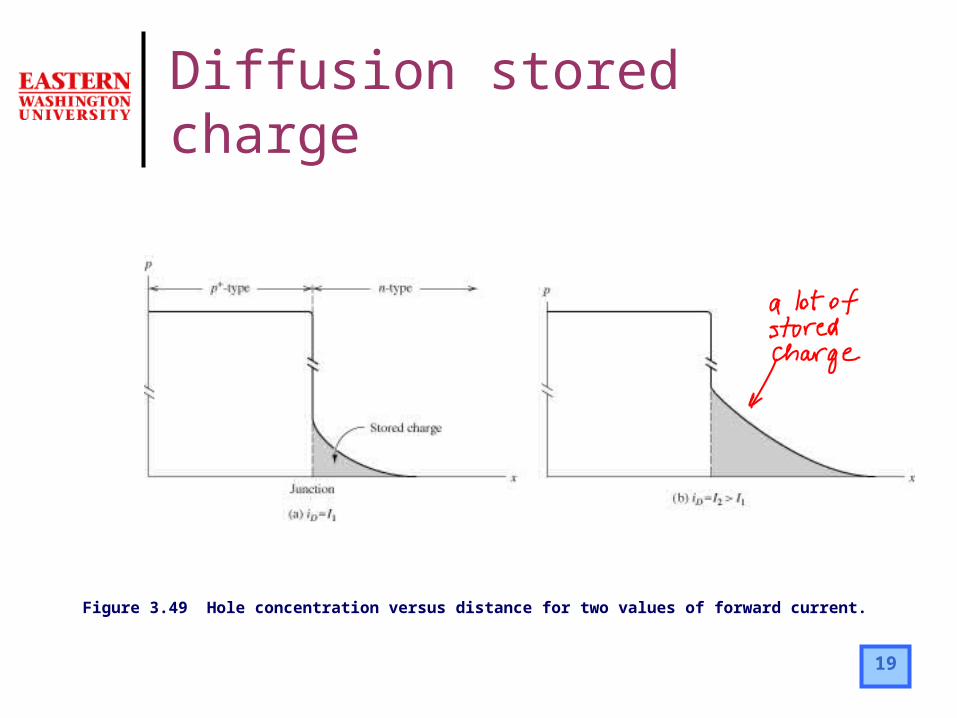
Figure 3.49 Hole concentration versus distance for two values of forward current.
Diffusion stored charge
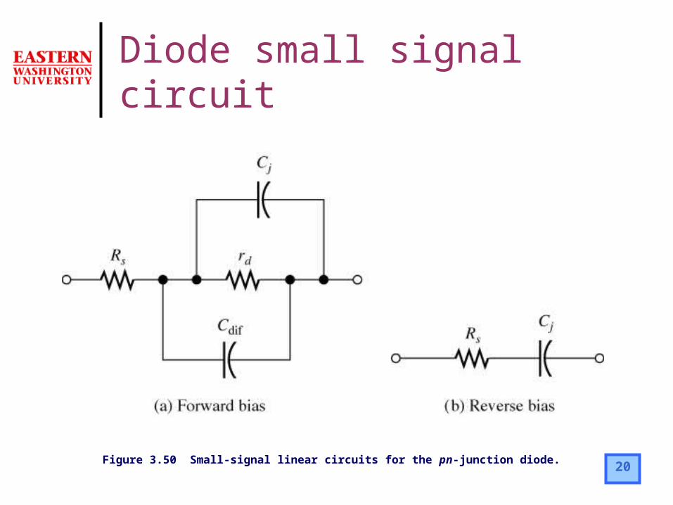
20Figure 3.50 Small-signal linear circuits for the pn-junction diode.
Diode small signal circuit

21Figure 3.51 Circuit illustrating switching behavior of a pn-junction diode.
Diode switching behavior (1)
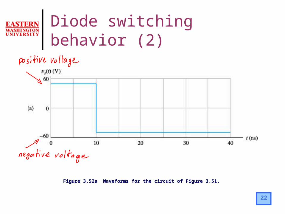
22
Figure 3.52a Waveforms for the circuit of Figure 3.51.
Diode switching behavior (2)

23
Figure 3.52b Waveforms for the circuit of Figure 3.51.
Diode switching behavior (3)

24Figure 3.53 Another set of waveforms for the circuit of Figure 3.51. Notice the absence of a storage interval.
Diode switching behavior (4)