1 synchronous sequential logic part ii logic and digital system design - cs 303 erkay savaş...
TRANSCRIPT

1
Synchronous Sequential LogicPart II
Logic and Digital System Design - CS 303Erkay Savaş
Sabancı University

2
State Reduction and Assignment
• In the design process of sequential circuits certain techniques are useful in reducing the circuit complexity– state reduction– state assignment
• State reduction– Fewer states fewer number of flip-flops– m flip-flops 2m states – Example: m = 5 2m = 32
• If we reduce the number of states to 21 do we reduce the number of flip-flops?

3
Example: State Reduction
Note that we useletters to designate the states forthe time being
a
b
d
f
c
eg
0/0
1/1
1/0
1/0
1/1
0/0
1/0
0/0
0/0
0/0
0/0
1/1
0/0
1/1
4
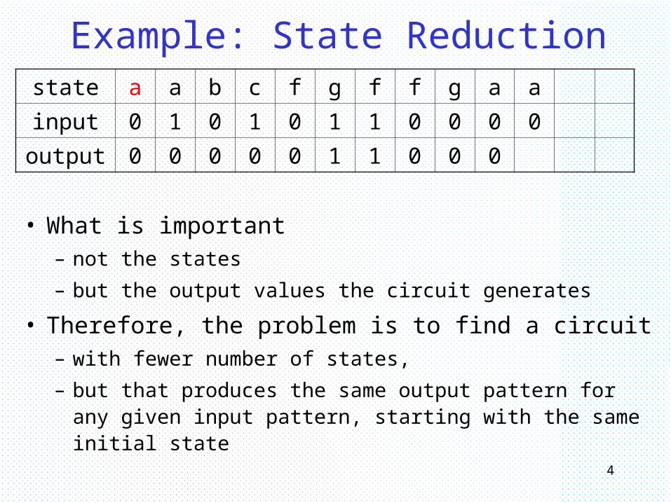
Example: State Reduction
• What is important– not the states
– but the output values the circuit generates
• Therefore, the problem is to find a circuit – with fewer number of states,
– but that produces the same output pattern for any given input pattern, starting with the same initial state
state a a b c f g f f g a a
input 0 1 0 1 0 1 1 0 0 0 0
output 0 0 0 0 0 1 1 0 0 0
5
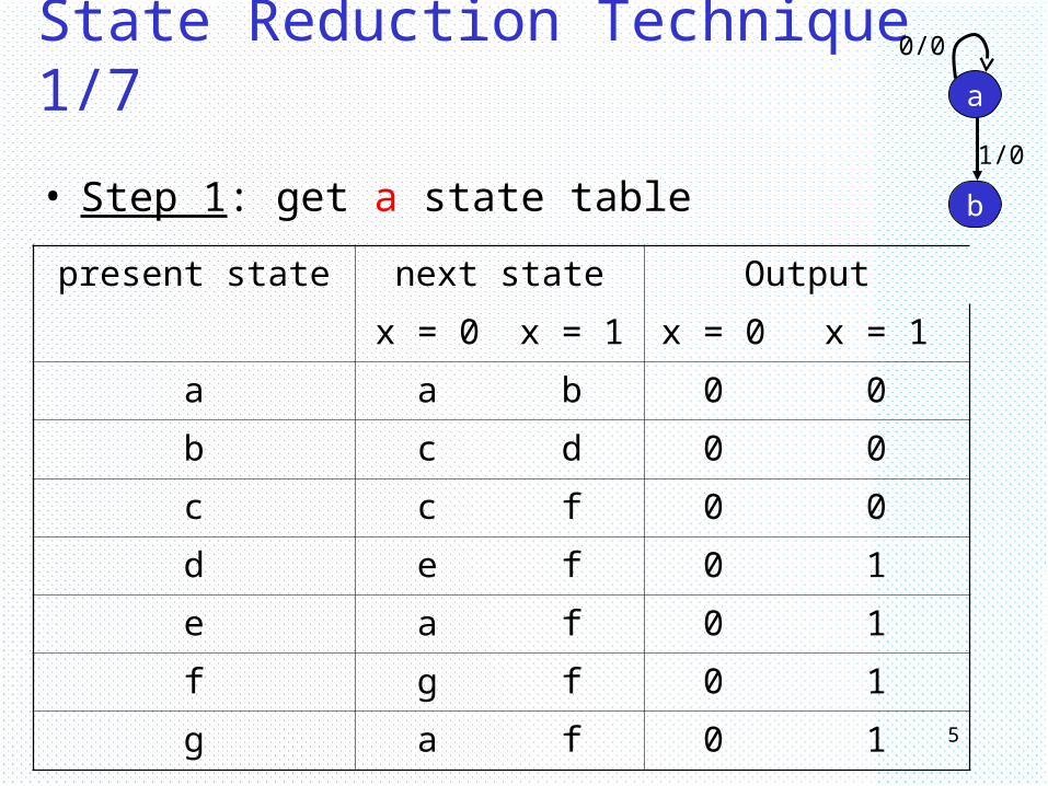
State Reduction Technique 1/7
• Step 1: get a state table
present state next state Output
x = 0 x = 1 x = 0 x = 1
a a b 0 0
b c d 0 0
c c f 0 0
d e f 0 1
e a f 0 1
f g f 0 1
g a f 0 1
a
b
0/0
1/0

6
State Reduction Technique 2/7
• Step 2: Inspect the state table for equivalent states– Equivalent states: Two states,
1. that produce exactly the same output2. whose next states are identical
– for each input combination

7
State Reduction Technique 3/7present state next state Output
x = 0 x = 1 x = 0 x = 1
a a b 0 0
b c d 0 0
c c f 0 0
d e f 0 1
e a f 0 1
f g f 0 1
g a f 0 1
• States “e” and “g” are equivalent• One of them can be removed
8
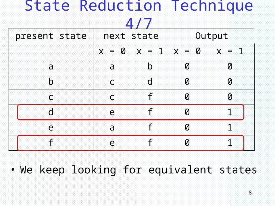
State Reduction Technique 4/7
• We keep looking for equivalent states
present state next state Output
x = 0 x = 1 x = 0 x = 1
a a b 0 0
b c d 0 0
c c f 0 0
d e f 0 1
e a f 0 1
f e f 0 1
9
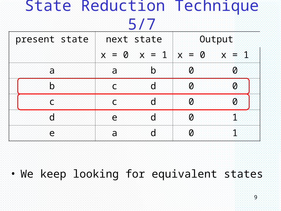
State Reduction Technique 5/7present state next state Output
x = 0 x = 1 x = 0 x = 1
a a b 0 0
b c d 0 0
c c d 0 0
d e d 0 1
e a d 0 1
• We keep looking for equivalent states
10
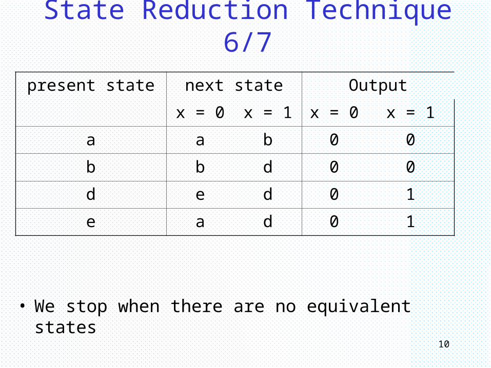
State Reduction Technique 6/7
• We stop when there are no equivalent states
present state next state Output
x = 0 x = 1 x = 0 x = 1
a a b 0 0
b b d 0 0
d e d 0 1
e a d 0 1

11
State Reduction Technique 7/7
a
b
d e
0/0
1/0
1/0
1/1
0/0
1/0
0/0
0/0
0/0
1/1We need two flip-flops
state a a b b d e d d e a a
input 0 1 0 1 0 1 1 0 0 0 0
output 0 0 0 0 0 1 1 0 0 0
present state
next state Output
x = 0 x = 1 x = 0 x = 1
a a b 0 0
b b d 0 0
d e d 0 1
e a d 0 1

12
State Assignments 1/4• We have to assign binary values to each state• If we have m states, then we need a code with
minimum n bits, where n = log2m
• There are different ways of encoding
• Example: Eight states: S0, S1, S2, S3, S4, S5 , S6 , S7
State Binary Gray One-hot
S0 000 000 000001
S1 001 001 000010
S2 010 011 000100
S3 011 010 001000
S4 100 110 010000
S5 101 111 100000
S6 111 101 100000
S7 111 100 100000

13
State Assignments 2/4• The circuit complexity depends on the state
encoding (assignment) scheme• Previous example: binary state encoding
present state next state Output
x = 0 x = 1 x = 0 x = 1
(a)00 00 01 0 0
(b) 01 01 10 0 0
(d) 10 11 10 0 1
(e) 11 00 10 0 1
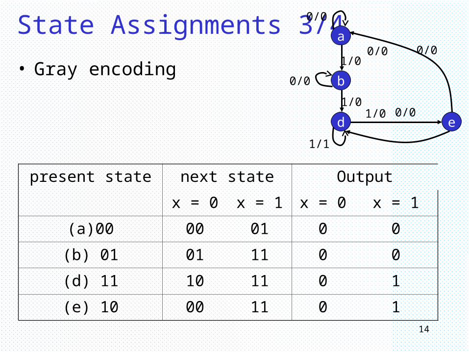
State Assignments 3/4
• Gray encoding
14
present state next state Output
x = 0 x = 1 x = 0 x = 1
(a)00 00 01 0 0
(b) 01 01 11 0 0
(d) 11 10 11 0 1
(e) 10 00 11 0 1
a
b
d e
0/0
1/0
1/0
1/1
0/0
1/0
0/0
0/0
0/0

State Assignments 4/4
• One-hot encoding
15
present state next state Output
x = 0 x = 1 x = 0 x = 1
(a)0001 0001 0010 0 0
(b) 0010 0010 0100 0 0
(d) 0100 1000 0100 0 1
(e) 1000 0001 0100 0 1

16
Designing Sequential Circuits
• Combinational circuits– can be designed given a truth table
• Sequential circuits– We need,
• state diagram or• state table
– Two parts• flip-flops: number of flip-flops is determined by
the number of states• combinational part:
– output equations– flip-flop input equations

17
Design Process
• Once we know the types and number of flip-flops, design process is reduced to design process of combinational circuits
• Therefore, we can apply the techniques of combinational circuit design
• The design steps1. Given a verbal description of desired
operation, derive state diagram2. Reduce the number of states if necessary
and possible3. State assignment
18
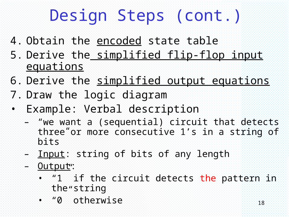
Design Steps (cont.)
4. Obtain the encoded state table5. Derive the simplified flip-flop input equations 6. Derive the simplified output equations7. Draw the logic diagram• Example: Verbal description
– “we want a (sequential) circuit that detects three or more consecutive 1’s in a string of bits”
– Input: string of bits of any length– Output:
• “1” if the circuit detects the pattern in the string
• “0” otherwise

19
Example: State Diagram
• Step 1: Derive the state diagram
S0 /0 S1/0
S2/0S3/1
01
0
10
1
1
0 Moore Machine

20
Synthesis with D Flip-Flops 1/5
• The number of flip-flops– Four states
– ? flip-flops
• State reduction– not possible in this case
• State Assignment– Use binary encoding
•S0 00
•S1 01
•S2 10
•S3 11
S0 /0 S1/0
S2/0S3/1
01
0
10
1
1
0
21
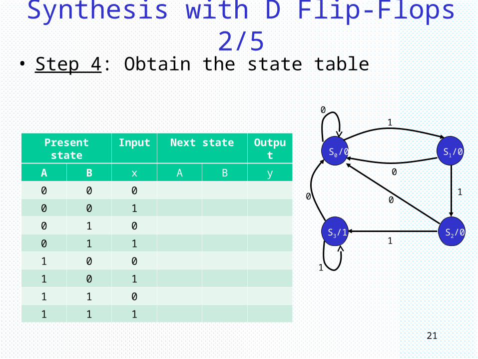
Synthesis with D Flip-Flops 2/5• Step 4: Obtain the state table
Present state Input Next state Output
A B x A B y
0 0 0
0 0 1
0 1 0
0 1 1
1 0 0
1 0 1
1 1 0
1 1 1
S0 /0 S1/0
S2/0S3/1
01
0
10
1
1
0

22
Synthesis with D Flip-Flops 3/5
• Step 5: Choose the flip-flops– D flip-flops
• Step 6: Derive the simplified flip-flop input equations– Boolean expressions for DA and DB
Present state
Input
Next state Output
A B x A B y
0 0 0 0 0 0
0 0 1 0 1 0
0 1 0 0 0 0
0 1 1 1 0 0
1 0 0 0 0 0
1 0 1 1 1 0
1 1 0 0 0 1
1 1 1 1 1 1
BxA 00 01 11 10
0 0 0 1 01 0 1 1 0
DA = Ax + Bx
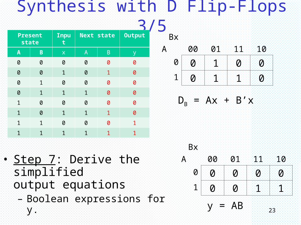
Synthesis with D Flip-Flops 3/5
23
BxA 00 01 11 10
0 0 1 0 01 0 1 1 0
DB = Ax + B’x
Present state
Input
Next state Output
A B x A B y
0 0 0 0 0 0
0 0 1 0 1 0
0 1 0 0 0 0
0 1 1 1 0 0
1 0 0 0 0 0
1 0 1 1 1 0
1 1 0 0 0 1
1 1 1 1 1 1
• Step 7: Derive the simplified output equations– Boolean expressions for y.
BxA 00 01 11 10
0 0 0 0 01 0 0 1 1
y = AB

24
Synthesis with D Flip-Flops 5/5
• Step 8: Draw the logic diagram
DA = Ax + Bx DB = Ax + B’x y = AB
D Q
CR
D Q
CR
A
B
y
DA
DB
x
clock reset
25
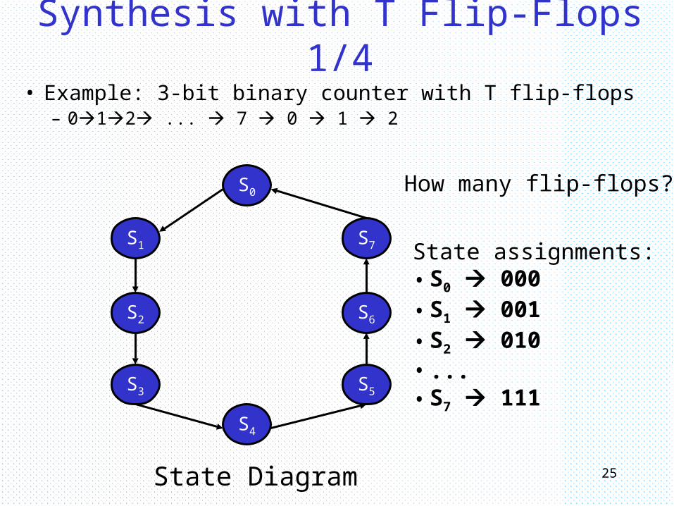
Synthesis with T Flip-Flops 1/4
• Example: 3-bit binary counter with T flip-flops– 012 ... 7 0 1 2
S0
S1 S7
S2 S6
S3 S5
S4
How many flip-flops?
State assignments:•S0 000•S1 001•S2 010•...•S7 111
State Diagram

26
Synthesis with T Flip-Flops 2/4
• State Table
000
111
011
101
001
110
010
100
111
011
101
001
110
010
100
000
T0T1T2A0A1A2A0A1A2
FF inputsnext statepresent state

Synthesis with T Flip-Flops 3/4Present state FF inputs
A2 A1 A0 T2 T1 T0
0 0 0 0 0 1
0 0 1 0 1 1
0 1 0 0 0 1
0 1 1 1 1 1
1 0 0 0 0 1
1 0 1 0 1 1
1 1 0 0 0 1
1 1 1 1 1 1
27
A1 A0
A200 01 11 10
0 0 0 1 01 0 0 1 0
• Flip-Flop input equations
T2 = A1A0
A1 A0
A200 01 11 10
0 0 1 1 01 0 1 1 0
T1 = A0
T0 = 1

28
Synthesis with T Flip-Flops 4/4
• Circuit
T2 = A1A0
T1 = A0
T0 = 1
A0T Q
CR
T Q
CR
T Q
CR
A1
A2
logic-1 T0
T1
T2
clock
reset

29
Synthesis with JK Flip-Flops 1/4
• State Table & JK FF Inputs
1X
0X
0X
0X
X0
X1
X0
1X
0X
X1
X0
0X
1X
X1
X0X0
00111
11011
11101
01001
10110
01010
10100
00000
KBJBKAJABAxBA
Flip-flop inputsnext stateInputPresent state
Q(t+1) = JQ’ + K’QJ K Q(t+1
)
0 0 Q
0 1 0
1 0 1
1 1 Q’

Synthesis with JK Flip-Flops 2/4
• Optimize the flip-flop input equations
BxA 00 01 11 10
0 0 0 0 11 X X X X
JA = Bx’
BxA 00 01 11 10
0 0 1 X X1 0 1 X X
JB = x
1X
0X
0X
0X
X0
X1
X0
1X
0X
X1
X0
0X
1X
X1
X0X0
00111
11011
11101
01001
10110
01010
10100
00000
KBJBKAJAB(t+1)A(t+1)xBA
Flip-flop inputs

Synthesis with JK Flip-Flops 3/4
31
BxA 00 01 11 10
0 X X X X1 0 0 1 0
KA = Bx
BxA 00 01 11 10
0 X X 0 11 X X 1 0
KB = (A x)’
1X
0X
0X
0X
X0
X1
X0
1X
0X
X1
X0
0X
1X
X1
X0X0
00111
11011
11101
01001
10110
01010
10100
00000
KBJBKAJAB(t+1)A(t+1)xBA
Flip-flop inputs

32
Synthesis with JK Flip-Flops 4/4• Logic diagram
JA = Bx’ KA = Bx JB = x KB = (A x)’
D Q
x
C
J Q
C
A
B
K
J Q
C
Kclk

33
Unused States
S0
S1
S2 S3
S4
Modulo-5 counter
Present State Next State
A B C A B C
0 0 0 0 0 1
0 0 1 0 1 0
0 1 0 0 1 1
0 1 1 1 0 0
1 0 0 0 0 0
34
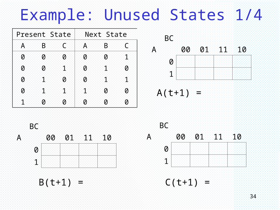
Example: Unused States 1/4Present State Next State
A B C A B C
0 0 0 0 0 1
0 0 1 0 1 0
0 1 0 0 1 1
0 1 1 1 0 0
1 0 0 0 0 0
BCA 00 01 11 10
0
1
A(t+1) =
BCA 00 01 11 10
0
1
B(t+1) =
BCA 00 01 11 10
0
1
C(t+1) =

35
Example: Unused States 2/4
010011
001111
000001
001110
110010
010100
100000
CBACBA
Next StatePresent State
A(t+1) = BC
B(t+1) = B C
C(t+1) = A’C’
000
001
010 011
100
101 110
111

36
Example: Unused States 3/4• Not using don’t care conditions
Present State Next State
A B C A B C
0 0 0 0 0 1
0 0 1 0 1 0
0 1 0 0 1 1
0 1 1 1 0 0
1 0 0 0 0 0
BCA 00 01 11 10
0 0 0 1 0
1 0 0 0 0
A(t+1) = A’BC
BCA 00 01 11 10
0 0 1 0 1
1 0 0 0 0
B(t+1) = A’B’C + A’BC’ = A’(B C)
BCA 00 01 11 10
0 1 0 0 1
1 0 0 0 0
C(t+1) = A’C’

37
Example: Unused States 4/4Present State Next State
A B C A B C
0 0 0 0 0 1
0 0 1 0 1 0
0 1 0 0 1 1
0 1 1 1 0 0
1 0 0 0 0 0
A(t+1) = A’BC
B(t+1) = A’(B C)
C(t+1) = A’C’
000
001
010 011
100
101 110 111

38
Sequential Circuit Timing 1/3
clk
D
Q
ts th
tp, FF
• It is important to analyze the timing behavior of a sequential circuit– Ultimate goal is to determine the maximum clock
frequency

39clock
inputs outputs
currentstate Flip-flop
inputs
Combinational Circuit
Flip-flops
DQ
C
Sequential Circuit Timing 2/3
ts
tp,COMB
tp,FF
tp,FF tp,COMB ts
clk
tp
tp = tp,FF + tp,COMB + ts

40clock
inputs outputs
currentstate Flip-flop
inputs
Combinational Circuit
Flip-flops
DQ
C
Sequential Circuit Timing 2/3
tp,COMB
tp,FF
tp,FF tp,COMB ts
clk
tp
tp,FF + tp,COMB >> th

41
Sequential Circuit Timing 3/3
• Minimum clock period (or maximum clock frequency)
tp
tp,FF tp,COMB ts
clk
tp,FF tp,COMB ts
tp
clk

42
Example: Sequential Circuit Timing
Find the longest path delay fromexternal input to the output
tp,XOR + tp,XOR = 2.0 + 2.0 = 4.0 ns
tp,NOT = 0.5 ns
tp,XOR = 2.0 ns
tp,AND = ts = 1.0 ns
th = 0.25 ns
tp,FF = 2.0 ns
D QC
B
xy
A
B’
clk

43
Example: Sequential Circuit Timing
Find the longest path delay in the circuit from external input to positive clock edge
tp,XOR + tp,NOT = 2.0 + 0.5 = 2.5 ns
tp,NOT = 0.5 ns
tp,XOR = 2.0 ns
tp,AND = ts = 1.0 ns
th = 0.25 ns
tp,FF = 2.0 ns
D QC
B
xy
A
B’
clk

44
Example: Sequential Circuit Timing
Find the longest path delay from positive clock edge to output
tp,FF + tp,XOR = 2.0 + 2.0 = 4.0 ns
tp,NOT = 0.5 ns
tp,XOR = 2.0 ns
tp,AND = ts = 1.0 ns
th = 0.25 ns
tp,FF = 2.0 ns
D QC
B
xy
A
B’
clk

45
Example: Sequential Circuit Timing
Find the longest path delay from positive clock edge to the flip-flop input
tp,FF + tp,AND + tp,XOR + tp,NOT
= 2.0 + 1.0 + 2.0 + 0.5 = 5.5 ns
tp,NOT = 0.5 ns
tp,XOR = 2.0 ns
tp,AND = ts = 1.0 ns
th = 0.25 ns
tp,FF = 2.0 ns
D QC
B
xy
A
B’
clk

46
Example: Sequential Circuit Timing
Determine the maximum frequency of operation of the circuit in megahertz
tp = tp,FF + tp,AND + tp,XOR + tp,NOT + ?
= 2.0 + 1.0 + 2.0 + 0.5 + 1.0 = 6.5 nsfmax = 1/tp = 1/(6.5×10-9) 154
MHz
tp,NOT = 0.5 ns
tp,XOR = 2.0 ns
tp,AND = ts = 1.0 ns
th = 0.25 ns
tp,FF = 2.0 ns
D QC
B
xy
A
B’
clk

47
Example
S0
S1 S2
S3
D QC
x1
D QC
x0
x0’
tp,XOR = 2.0 ns
tp,FF = 2.0 ns
ts = 1.0 ns
tp = tp,FF + tp,XOR + ts = 2.0 + 2.0 + 1.0 = 5.0 ns
fmax = 1/tp = 1/(5.0×10-9) 200 MHz
Binary encoding

48
Example: One-Hot-Encoding
S0 0001S1 0010S2 0100S3 1000
D QC
y0
D QC
D QC
D QC
y1
y2
y3
tp,FF = 2.0 ns
ts = 1.0 ns
tp = tp,FF + ts = 2.0 + 1.0 =
3.0 nsfmax = 1/tp = 1/(3.0×10-9) 333 MHz