1.0 general single-stage small-signal amplifier design...
TRANSCRIPT
1
May 2008 2006 by Fabian Kung Wai Lee 1
8D - General Single-Stage
Small-Signal Amplifier
Design
The information in this work has been obtained from sources believed to be reliable.The author does not guarantee the accuracy or completeness of any informationpresented herein, and shall not be responsible for any errors, omissions or damagesas a result of the use of this information.
May 2008 2006 by Fabian Kung Wai Lee 2
1.0 General Single-Stage
Small-Signal Amplifier
Design Procedures
2
May 2008 2006 by Fabian Kung Wai Lee 3
Practical Single-Stage Small-Signal
Amplifier Design (1)
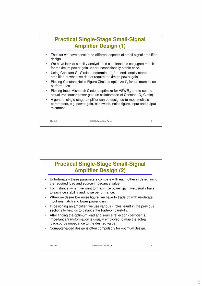
• Thus far we have considered different aspects of small-signal amplifier
design.
• We have look at stability analysis and simultaneous conjugate match
for maximum power gain under unconditionally stable case.
• Using Constant GP Circle to determine ΓL for conditionally stable
amplifier, or when we do not require maximum power gain.
• Plotting Constant Noise Figure Circle to optimize Γs for optimum noise
performance.
• Plotting Input Mismatch Circle to optimize for VSWRin and to set the
actual transducer power gain (in collaboration of Constant Gp Circle).
• A general single-stage amplifier can be designed to meet multiple
parameters, e.g. power gain, bandwidth, noise figure, input and output
mismatch.
May 2008 2006 by Fabian Kung Wai Lee 4
Practical Single-Stage Small-Signal
Amplifier Design (2)
• Unfortunately these parameters compete with each other in determining
the required load and source impedance value.
• For instance, when we want to maximize power gain, we usually have
to sacrifice stability and noise performance.
• When we desire low noise figure, we have to trade off with moderate
input mismatch and lower power gain.
• In designing an amplifier, we use various circles learnt in the previous
sections to help us to balance the trade-off carefully.
• After finding the optimum load and source reflection coefficients,
impedance transformation is usually employed to map the actual
load/source impedance to the desired value.
• Computer-aided design is often compulsory for optimum design.
3
May 2008 2006 by Fabian Kung Wai Lee 5
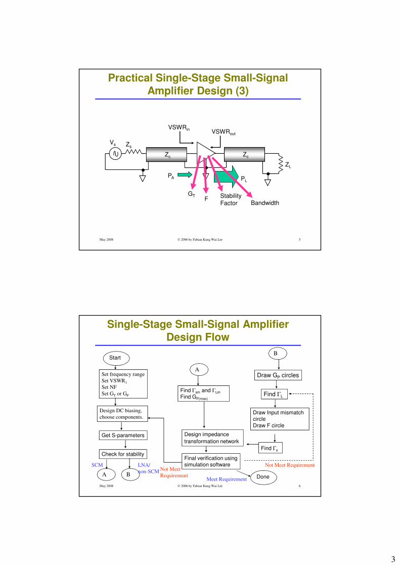
Practical Single-Stage Small-Signal
Amplifier Design (3)
ZL
ZcZc
ZsVs
VSWRinVSWRout
PA PL
GTF
Stability
Factor Bandwidth
May 2008 2006 by Fabian Kung Wai Lee 6
Single-Stage Small-Signal Amplifier
Design Flow
SCM
Start
Set frequency range
Set VSWR1
Set NF
Set GT or GP
Get S-parameters
Design DC biasing,
choose components.
Check for stability
Find Γsm and ΓLm
Find GP(max)
Design impedance
transformation network
Final verification usingsimulation software
Draw GP circles
Draw Input mismatchcircleDraw F circle
Find ΓL
Done
Find Γs
Meet Requirement
Not Meet
RequirementA B
LNA/
non-SCM
A
B
Not Meet Requirement

4
May 2008 2006 by Fabian Kung Wai Lee 7
Summary for Chapter 7 & 8
−−= 12
12
21(max) KK
S
SGP
( )
*22111
2222
2111
21
211
1
1
42
1 21
DSSB
DSSA
BAAB
Sm
−=
−−+=
−−=Γ ( )
*11222
2211
2222
22
222
2
1
42
1 21
DSSB
DSSA
BAAB
Lm
−=
−−+=
−−=Γ
• Stability Factor check for unconditionally stable amplifier:
• Simultaneous Conjugate Match:
• Only when amplifier is unconditionally stable, K>1 .
1 12
1
2112
2222
211
<>+−−
= DSS
DSSK
Sets both ΓL and Γs
May 2008 2006 by Fabian Kung Wai Lee 8
Summary for Chapter 7 & 8
• Constant Power Gain:
• Can be applied for both unconditionally stable and conditionally stable
amplifier.
*11222 DSSC −=
( ) ( )
22
22
22
22
22
22
22
22
1
Im
1
Re
gDgS
Cgj
gDgS
CgT
PG+−−
++−−
−=
221
2S
Gg P=
22
22
22
22
2211222112
1
21
gDgS
gSSgSSKR
PG+−−
+−=
12
21)(
S
SG MSGP =
Sets ΓL
5
May 2008 2006 by Fabian Kung Wai Lee 9
Summary for Chapter 7 & 8
• Constant Noise Figure:
22mS
s
immS
s
im YY
G
RFZZ
R
GFF −+=−+=
( ) ( )
io
mm
e
mmoi
GZ
FF
R
FFZN
4
1
4
122
Γ+−=
Γ+−=
i
mFcenter
N+
Γ=Γ
1
i
mii
FradN
NN
R+
Γ−+
=1
122
Sets Γs
May 2008 2006 by Fabian Kung Wai Lee 10
Summary for Chapter 7 & 8
• Constant Input Mismatch:
( ) 211
*11
11 Γ−−
Γ=Γ
M
MScenter
( ) 211
211
11
11
Γ−−
Γ−−
=M
M
RSrad
PT GMG 1=2
1
21
2
11
11
s
sM
ΓΓ−
Γ−
Γ−
=
1
111
2
M-1-1
M-11VSWR 1
+==− Mρ
2
1
11
1
11
+
−−=
VSWR
VSWRM
Sets Γs
6
May 2008 2006 by Fabian Kung Wai Lee 11
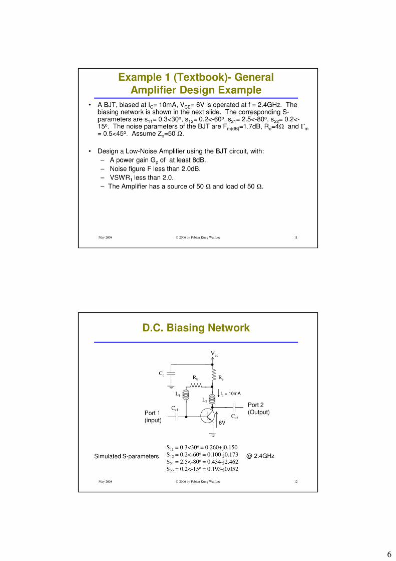
Example 1 (Textbook)- General
Amplifier Design Example
• A BJT, biased at IC= 10mA, VCE= 6V is operated at f = 2.4GHz. The biasing network is shown in the next slide. The corresponding S-parameters are s11= 0.3<30o, s12= 0.2<-60o, s21= 2.5<-80o, s22= 0.2<-15o. The noise parameters of the BJT are Fm(dB)=1.7dB, Re=4Ω and Γm
= 0.5<45o. Assume Zo=50 Ω.
• Design a Low-Noise Amplifier using the BJT circuit, with:
– A power gain Gp of at least 8dB.
– Noise figure F less than 2.0dB.
– VSWR1 less than 2.0.
– The Amplifier has a source of 50 Ω and load of 50 Ω.
May 2008 2006 by Fabian Kung Wai Lee 12
D.C. Biasing Network
S11 = 0.3<30o = 0.260+j0.150
S12 = 0.2<-60o = 0.100-j0.173
S21 = 2.5<-80o = 0.434-j2.462
S22 = 0.2<-15o = 0.193-j0.052
Cc1
Cc2
L1
L2
CdRc
Vcc
Rb
Port 1
(input)
Port 2
(Output)
Ic = 10mA
6V
@ 2.4GHzSimulated S-parameters

7
May 2008 2006 by Fabian Kung Wai Lee 13
General Amplifier Design Example
• Stability Analysis : K=1.178 > 1 and |D|=0.555 < 1. So the amplifier is
unconditionally stable and the maximum power gain is:
• So the power gain fulfills the requirement. This is the value that can be
obtained if we apply Simultaneous Conjugate Match (SCM). In this
case Gp = GT = GA.
• Computing the source and load impedance for maximum power gain:
• For the next step, we will plot the constant input mismatch circles and
constant noise figure (F) circles on the Smith chart for Γs plane, with ΓL
= ΓLm.
• Then we make sure that the location of Γsm fulfill the requirements of F
< 2.0dB and VSWR1 < 2.0.
( ) 8.42dBor 942.612
12
21
(max) =−−= KKs
sGP
1157.00444.0
091.02815.0
j
j
Lm
sm
+=Γ
−=Γ
May 2008 2006 by Fabian Kung Wai Lee 14
General Amplifier Design Cont...
*1 091.02815.0 smj Γ=+=Γ
• For ΓL = ΓLm:
• Now with this information we could calculate the radius and center of
the constant input mismatch or VSWR1 circles.
8
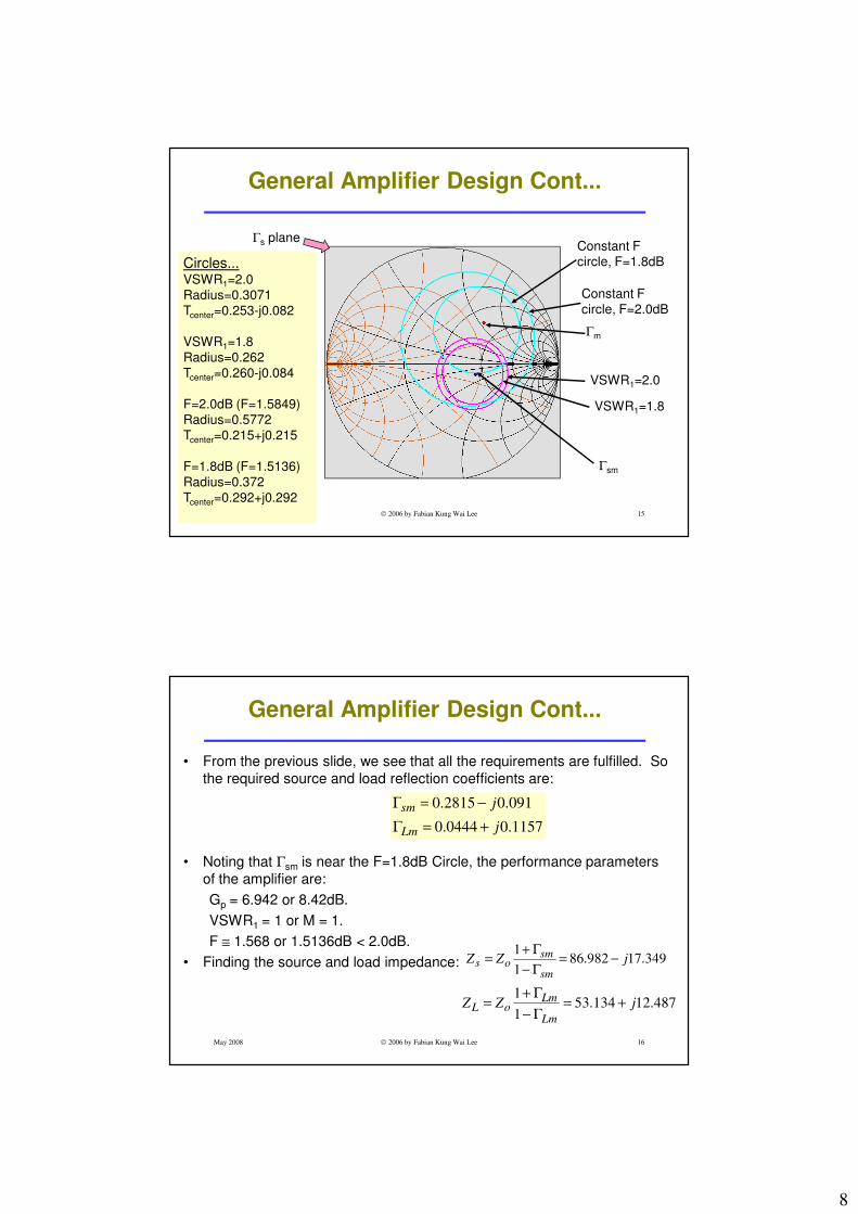
May 2008 2006 by Fabian Kung Wai Lee 15
General Amplifier Design Cont...
Γs plane
Circles...VSWR1=2.0
Radius=0.3071
Tcenter=0.253-j0.082
VSWR1=1.8
Radius=0.262
Tcenter=0.260-j0.084
F=2.0dB (F=1.5849)
Radius=0.5772
Tcenter=0.215+j0.215
F=1.8dB (F=1.5136)
Radius=0.372
Tcenter=0.292+j0.292
Constant F
circle, F=2.0dB
Γm
Constant F
circle, F=1.8dB
VSWR1=2.0
Γsm
VSWR1=1.8
May 2008 2006 by Fabian Kung Wai Lee 16
General Amplifier Design Cont...
• From the previous slide, we see that all the requirements are fulfilled. So
the required source and load reflection coefficients are:
• Noting that Γsm is near the F=1.8dB Circle, the performance parameters
of the amplifier are:
Gp = 6.942 or 8.42dB.
VSWR1 = 1 or M = 1.
F ≅ 1.568 or 1.5136dB < 2.0dB.
• Finding the source and load impedance:
1157.00444.0
091.02815.0
j
j
Lm
sm
+=Γ
−=Γ
349.17982.861
1jZZ
sm
smos −=
Γ−
Γ+=
487.12134.531
1jZZ
Lm
LmoL +=
Γ−
Γ+=
9
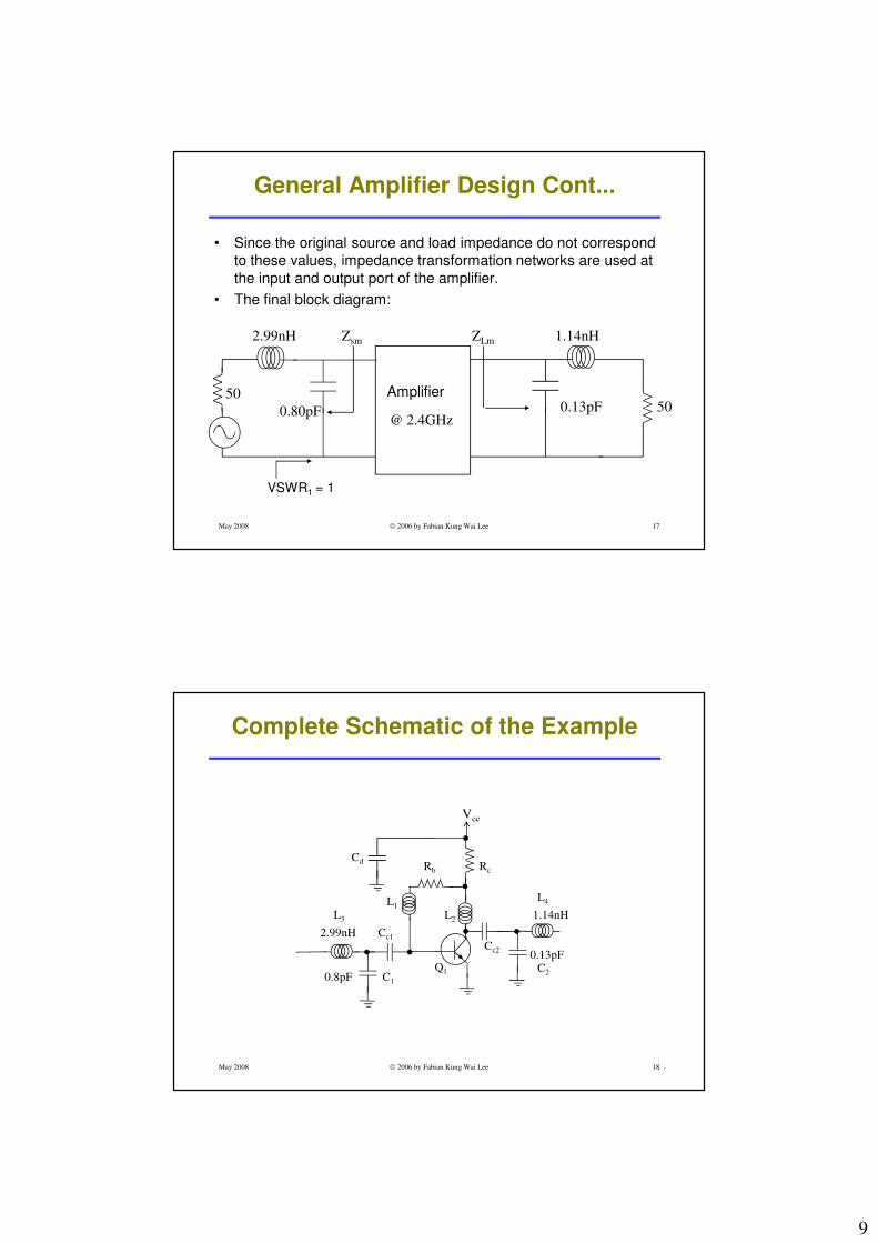
May 2008 2006 by Fabian Kung Wai Lee 17
General Amplifier Design Cont...
• Since the original source and load impedance do not correspond
to these values, impedance transformation networks are used at
the input and output port of the amplifier.
• The final block diagram:
Amplifier50
2.99nH
0.80pF 50
Zsm ZLm
@ 2.4GHz
1.14nH
0.13pF
VSWR1 = 1
May 2008 2006 by Fabian Kung Wai Lee 18
Complete Schematic of the Example
Cc1
Cc2
L1
L2
CdRc
Vcc
Rb
2.99nH
0.8pF
1.14nH
0.13pFQ1 C2
L4
L3
C1
10
May 2008 2006 by Fabian Kung Wai Lee 19
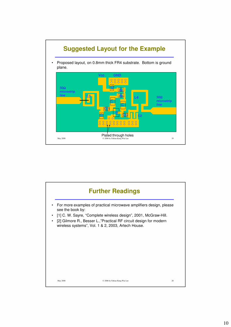
Suggested Layout for the Example
• Proposed layout, on 0.8mm thick FR4 substrate. Bottom is ground
plane.
Vcc GND
Cc2
Cc1
C1
Q1
L3 L4
C2
50ΩΩΩΩ
microstrip line
50ΩΩΩΩ
microstrip line
Rc
Cd
L1
L2
Rb
Plated through holes
May 2008 2006 by Fabian Kung Wai Lee 20
Further Readings
• For more examples of practical microwave amplifiers design, please
see the book by:
• [1] C. W. Sayre, “Complete wireless design”, 2001, McGraw-Hill.
• [2] Gilmore R., Besser L.,”Practical RF circuit design for modern
wireless systems”, Vol. 1 & 2, 2003, Artech House.
11
May 2008 2006 by Fabian Kung Wai Lee 21
2.0 Practical Amplifier
Design Example - Low-
Noise Amplifier with Fixed
GT and Input Mismatch
May 2008 2006 by Fabian Kung Wai Lee 22
Introduction
• In this exercise we are going to design and built a low-noise amplifier,
optimized for operation at 850 to 920 MHz.
• The RF transistor BFR92A is used for this exercise. This is a wideband
NPN transistor with fT = 5 GHz (at IC = 30 mA and VCE = 10 V). Using a
transistor with fT > 5×fo allows us to reduce the dc collector current (IC),
thereby reducing idle power dissipation.
• The circuit is intended for operation at a supply voltage of 3.0 to 3.3 V.
• The software Advanced Design System, ADS2003C from Agilent
Technologies is used for the computer analysis.
12
May 2008 2006 by Fabian Kung Wai Lee 23
D.C. Biasing Design (1)
• Voltage feedback
bias is chosen.
• AppCAD is used
to estimate the
initial biasing
resistor values and
to perform the
necessary d.c.
stability analysis
From Datasheet
of BFR92A
D.c. stability analysis
results
May 2008 2006 by Fabian Kung Wai Lee 24
D.C. Biasing Design (2)
3 V
778 mV
778 mV
1.33 V
1.33 V 1.33 V
DC
DC1
DC-3.55 mA
V_DC
SRC1
Vdc=3.0 V
2.99 mA
36.1 uA
-3.03 mA
pb_phl_BFR92A_19921214
Q1519 uA
R
RB2
R=1.5 kOhm
555 uA
R
RB1
R=1 kOhm
3.55 mA
R
RC
R=470 Ohm
Simulated result using
nonlinear d.c. solver, with
SPICE model of BFR92A
IC = 3.0mA
VCE= 1.33V
Theoretical max voltage
swing at collector of Q1 =
2x1.33 = 2.66V

13
May 2008 2006 by Fabian Kung Wai Lee 25
A.C. Analysis (1)
• Upon adding in RF choke LC and
coupling capacitors Cc1 and Cc2,
small-signal a.c. simulation
(S-parameters) is performed from
100MHz to 3000MHz.
• Note that noise calculation is enabled
and the Roulette K factor macro is
also inserted.
S_Param
SP1
NoiseOutputPort=2
NoiseInputPort=1
CalcNoise=yes
Step=2.0 MHz
Stop=3.0 GHz
Start=100 MHz
S-PARAMETERS
StabFact
StabFact1
K=stab_fact(S)
StabFactL
LC
R=
L=100.0 nH
R
RC
R=470 Ohm
V_DC
SRC1
Vdc=3.0 V
Term
Term2
Z=50 Ohm
Num=2
C
Cc2
C=100.0 pF
Term
Term1
Z=50 Ohm
Num=1
C
Cc1
C=100.0 pF
pb_phl_BFR92A_19921214
Q1
R
RB2
R=1.5 kOhm
R
RB1
R=1 kOhm
May 2008 2006 by Fabian Kung Wai Lee 26
A.C. Analysis (2)
m1freq=m1=10.024
900.0MHzm2freq=m2=-18.719
900.0MHzm1freq=m1=10.024
900.0MHzm2freq=m2=-18.719
900.0MHz
0.2 0.4 0.6 0.8 1.0 1.2 1.4 1.6 1.8 2.0 2.2 2.4 2.6 2.80.0 3.0
-20
-15
-10
-5
0
5
10
15
-25
20
freq, GHz
dB(S(2,1))
m1
dB(S(1,2))
m2
m3freq=m3=0.441 / -22.718impedance = Z0 * (2.114 - j0.893)
898.0MHz
m4freq=m4=0.309 / -129.050impedance = Z0 * (0.610 - j0.323)
900.0MHz
m3freq=m3=0.441 / -22.718impedance = Z0 * (2.114 - j0.893)
898.0MHz
m4freq=m4=0.309 / -129.050impedance = Z0 * (0.610 - j0.323)
900.0MHz
freq (100.0MHz to 3.000GHz)
S(1,1)
m4
S(2,2)
m3
S21 of the a.c. analysis indicates
power gain Gp of greater than
9dB between 800 to 900 MHz.

14
May 2008 2006 by Fabian Kung Wai Lee 27
A.C. Analysis (3)
0.5 1.0 1.5 2.0 2.50.0 3.0
0.4
0.6
0.8
1.0
1.2
0.2
1.4
freq, GHzK
mag(D)
Eqn D=S11*S22-S12*S21
m5freq=m5=1.263
894.0MHzm5freq=m5=1.263
894.0MHz
0.2 0.4 0.6 0.8 1.0 1.2 1.4 1.6 1.8 2.0 2.2 2.4 2.6 2.80.0 3.0
2
3
1
4
freq, GHz
NFmin
m5
nf(2)
• Furthermore the basic
amplifier circuit is uncon-
ditionally stable. As indicated
by K > 1 and |D| < 1 within
the analysis frequency range.
• We do not have to worry about
stability greater than 3GHz as
for the d.c. biasing used,
transistor Q1 fT is expected to be
less than 3GHz.
• Also noise calculation shows
that theoretically a noise figure
of less than 1.26 can be
achieved.
Noise Figure (dB)
Minimum Noise
Figure
May 2008 2006 by Fabian Kung Wai Lee 28
A.C. Analysis at 900MHz (1)
SmGamma2
SmGamma1
SmGammaL=sm_gamma2(S)
SmGamma2
N
GpCircle
GpCircle1
GpCircle1=gp_circle(S,8,10,12,51)
GpCircle
NsCircle
NsCircle1
NFCircle=ns_circle(NFmin+0.1,0.3,NFmin,Sopt,Rn/50,51)
NsCircle
StabFact
StabFact1
K=stab_fact(S)
StabFact
S_Param
SP1
NoiseOutputPort=2
NoiseInputPort=1
CalcNoise=yes
CalcZ=yes
Step=2.0 MHz
Stop=900.0 MHz
Start=900 MHz
S-PARAMETERS
L
LC
R=
L=100.0 nH
R
RC
R=470 Ohm
V_DC
SRC1
Vdc=3.0 V
Term
Term2
Z=50 OhmNum=2
C
Cc2
C=100.0 pF
Term
Term1
Z=50 Ohm
Num=1
C
Cc1C=100.0 pF
pb_phl_BFR92A_19921214
Q1
R
RB2
R=1.5 kOhm
R
RB1
R=1 kOhm
To find ΓLat Gp(max)
To generate points forconstant Gp circles for Gp = 8, 10 and 12dB
To generate pointsfor constant F circlesfor F = Fmin+0.1 andFmin+0.3
Start and stop at 900MHz,also enable computationof Z parameters
The target is to operate
the amplifier in the
vicinity of 900MHz, thus
we focus the analysis
at this frequency.
15
May 2008 2006 by Fabian Kung Wai Lee 29
A.C. Analysis at 900MHz (2)
Eqn Rminput = (sqrt(1-Minput)*(1-mag(T1)*mag(T1)))/(1-(1-Minput)*mag(T1)*mag(T1))
Eqn TL = m1
Eqn T1 = (S11-D*TL)/(1-S22*TL)
Eqn D=S11*S22-S12*S21
Eqn Tmcenter=(Minput*conj(T1))/(1-(1-Minput)*mag(T1)*mag(T1))
Eqn Theta= generate(0,2*PI,51)
Eqn Minput_Circle = Tmcenter+Rminput*exp(j*Theta)
Eqn Zo=50
Eqn Ts =m2
Macro to generate Constant Input Mismatch Circle
• We write our own macro to generate points for constant Input Mismatch
circle on Smith Chart for Γs. Here m1 and m2 are markers in the Smith
Charts.
• Minput is the user specified Input Mismatch Factor.
May 2008 2006 by Fabian Kung Wai Lee 30
A.C. Analysis at 900MHz (3)
Two Smith Charts are plotted. Markers m1 and m2 are chosen such that power
gain Gp=12.0dB and noise figure F is the minimum. As marker m1 changes, the
constant Input Mismatch Circle size and position on Γs plane change accordingly.
m2indep(m2)=m2=0.344 / 158.973indep(__d, 2)=0impedance = Z0 * (0.501 + j0.140)
40m2indep(m2)=m2=0.344 / 158.973indep(__d, 2)=0impedance = Z0 * (0.501 + j0.140)
40
freq (900.0MHz to 900.0MHz)
Sopt
cir_pts (0.000 to 51.000)
NFCircle
indep(Minput_Circle) (0.000 to 50.000)
Minput_Circle m2
m1indep(m1)=m1=0.451 / 42.317gain=12.000000impedance = Z0 * (1.485 + j1.133)
28m1indep(m1)=m1=0.451 / 42.317gain=12.000000impedance = Z0 * (1.485 + j1.133)
28
cir_pts (0.000 to 51.000)
GpCircle1
m1
freq (900.0MHz to 900.0MHz)
SmGammaL
Γs plane ΓL plane
Constant Gp
circles
ΓLm
Constant InputMismatch circle
Constant Fcircles
Sopt, S11 forlowest noisefigure NFmin

16
May 2008 2006 by Fabian Kung Wai Lee 31
A.C. Analysis at 900MHz (4)
• From the Smith Charts, after some tuning, the chosen load and source
impedance are as shown.
• Observe that transducer power gain GT = Minput x Gp. Or in dB
GTdB = 10log(Minput) + 10log(Gp) = -0.458 + 12 = 11.542
• Noise figure of better than 1.264+0.1 dB can be achieved.
freq
900.0MHz
Sopt
-0.231 + j0.218
Rn
5.117
nf(2)
1.468
NFmin
1.264
Eqn Minput = 0.95Input Mismatch Factor
Eqn ZL = Zo*(1+TL)/(1-TL)
ZL74.248 + j56.640
Zs27.924 + j9.515
Eqn Zs = Zo*(1+m2)/(1-m2)
Eqn GT=((1-pow(mag(TL),2))*pow(mag(S21),2)*(1-pow(mag(Ts),2)))/(pow(mag(1-S22*TL),2)*pow(mag(1-T1*Ts),2))
GT_dB
11.777
K
1.105
freq
900.0MHz
Eqn GT_dB = 10*log(GT)
Small-signal requirement of Amplifer: NOTE: 1. Set a reasonable input mismatch factor "Minput" (between 0 to 1).2. Move marker m1 along constant Gp circles to obtainsuitable load impedance and m2 along the constant input mismatchcircle to obtain suitable source impedance.
Noise parameters:
May 2008 2006 by Fabian Kung Wai Lee 32
Input and Output Impedance
Transformation Network
The following LC networks are used:
1. Load Network: to transform ZL = 50 to 74+j57 (approximate) at 900MHz.
2. Source Network: to transform Zs = 50 to 28+j10 (approximate) at 900MHz.
Port
Load
Num=1
L
L1
R=
L=10.2 nHC
C1
C=0.68 pF
R
RL
R=50 Ohm
Port
Source
Num=1
L
L1
R=
L=6.16 nHC
C1
C=3.13 pF
R
Rs
R=50 Ohm
Load network Source network
17
May 2008 2006 by Fabian Kung Wai Lee 33
The Complete Schematic
L
Lm2
R=
L=2.2 nH
S_Param
SP1
NoiseOutputPort=2
NoiseInputPort=1
CalcNoise=yes
CalcZ=yes
Step=2.0 MHz
Stop=1600.0 MHz
Start=200 MHz
S-PARAMETERS
Term
Term2
Z=50 Ohm
Num=2
StabFact
StabFact1
K=stab_fact(S)
StabFact
L
Lm3
R=
L=10.0 nH
C
Cm2
C=0.68 pF
C
Cc2
C=100.0 pF
pb_phl_BFR92A_19921214
Q1
C
Cm1
C=3.3 pF
Term
Term1
Z=50 Ohm
Num=1
L
Lm1
R=
L=4.7 nH
C
Cc1
C=100.0 pF R
RB2
R=1.5 kOhm
R
RB1
R=1 kOhm
L
LC
R=
L=100.0 nH
R
RC
R=470 Ohm
V_DC
SRC1
Vdc=3.0 V
Practical L and C values are used to approximate the source and load
transformation networks
May 2008 2006 by Fabian Kung Wai Lee 34
A.C. Analysis of the Complete
Schematic
The small-signal performance
of the matched circuit, from
200 to 1600MHz
Important parameters at 900MHz:
m1freq=m1=11.858
900.0MHzm1freq=m1=11.858
900.0MHz
0.3 0.4 0.5 0.6 0.7 0.8 0.9 1.0 1.1 1.2 1.3 1.4 1.50.2 1.6
-25
-20
-15
-10
-5
0
5
10
15
-30
20
freq, GHz
GT_dB
m1
dB(S(1,2))
0.3 0.4 0.5 0.6 0.7 0.8 0.9 1.0 1.1 1.2 1.3 1.4 1.50.2 1.6
1.5
1.0
2.0
freq, GHz
NFmin
nf(2)
freq
900.0MHz
nf(2)
1.267
GT_dB
11.858
dB(S(1,1))
-15.857
dB(S(2,2))
-15.714
K
1.105

18
May 2008 2006 by Fabian Kung Wai Lee 35
Large Signal A.C. Analysis – Gain
Compression (1)
VL
Vin
P_1Tone
PORT1
Freq=RF_f req MHz
P=polar(dbmtow(Pin),0)
Z=50 Ohm
Num=1
R
RL
R=50 Ohm
HarmonicBalance
HB1
Step=1
Stop=10
Start=-30
SweepVar="Pin"
Order[1]=6
Freq[1]=RF_f req MHz
HARMONIC BALANCE
VAR
VAR1
RF_f req=900
Pin=-30
EqnVar
L
Lm2
R=
L=2.2 nH
I_Probe
I_in
L
Lm3
R=
L=10.0 nH
C
Cm2
C=0.68 pF
C
Cc2
C=100.0 pF
pb_phl_BFR92A_19921214
Q1
C
Cm1
C=3.3 pF
L
Lm1
R=
L=4.7 nH
C
Cc1
C=100.0 pF R
RB2
R=1.5 kOhm
R
RB1
R=1 kOhm
L
LC
R=
L=100.0 nH
R
RC
R=470 Ohm
V_DC
SRC1
Vdc=3.0 V
• Finally a large-signal frequency domain analysis is carried out using Harmonic
Balance method.
• Input available power Pin is swept from -30dBm to 10dBm.
Pin is swept
Consider upTo 5th harmonic
May 2008 2006 by Fabian Kung Wai Lee 36
Large Signal A.C. Analysis – Gain
Compression (2)
Eqn PL1 = 0.5*(pow(mag(VL[1]),2)/RL)
Eqn RL=Zo
Eqn Pin1=0.5*(real(Vin[1]*conj(I_in.i[1])))
Eqn Zo = 50
Eqn GA1_dB = 10*log(PL1) - (Pin-30)
Eqn Zin1 = Vin[1]/I_in.i[1]
Eqn PL1_dBm = 10*log(PL1)+30
• Node voltages VL, Vin and current I_in are arrays.
• The following equations are used to compute the load power PL1 and input
power Pin1 at fundamental frequency (RF_freq).Index = 0: d.c.Index = 1: FundamentalIndex = 2: 1st HarmonicIndex = 3: 2nd Harmonicetc…
Power in dBm!
19
May 2008 2006 by Fabian Kung Wai Lee 37
Large Signal A.C. Analysis – Gain
Compression (3)
-25 -20 -15 -10 -5 0 5-30 10
0
5
10
-5
15
Pin
GA1_dB
-25 -20 -15 -10 -5 0 5-30 10
-15
-10
-5
0
5
10
15
20
-20
25
Pin
PL1_dBm_Ideal
PL1_dBm
Eqn GradPL1 = (PL1_dBm[2]-PL1_dBm[0])/(Pin[2]-Pin[0])
Eqn CPL1 = PL1_dBm[0]
Eqn PL1_dBm_Ideal = GradPL1*(Pin-Pin[0])+CPL1
-25 -20 -15 -10 -5 0 5-30 10
-10
0
10
20
30
40
-20
50
Pin
real(Zin1)
imag(Zin1)
PL1_dBm_Ideal[intI]
-0.184
PL1_dBm[intI]
-1.390
Pin[intI]
-12.000
Eqn intI = 18
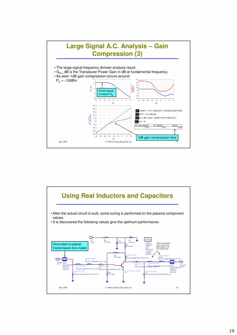
• The large-signal frequency domain analysis result.
• GA1_dB is the Transducer Power Gain in dB at fundamental frequency.
• As seen 1dB gain compression occurs around
Pin = -12dBm
1dB gain compression here
Small signal,
constant GA
May 2008 2006 by Fabian Kung Wai Lee 38
Using Real Inductors and Capacitors
• After the actual circuit is built, some tuning is performed on the passive component
values.
• It is discovered the following values give the optimum performance.
RRB2
R=1.5 kOhm
R
RCR=470 Ohm
RRD1
R=100 Ohm CPWSUB
CPWSub1
Rough=0 mil
TanD=0T=1.38 mil
Cond=5.7E+8Mur=1
Er=4.6
H=62.0 mil
CPWSubCCd2
C=100.0 pF
CCd3
C=22.0 pF
Port
RF_inputNum=1 Port
RF_output
Num=2
b82496c3100j000
L3Part_Num=SIMID 0603-C (10 nH +-5%)
NPO_0603_0_68pFC2
Part_Num=Phycomp NPO 0603 0.68pF +-5%
NPO_0603_3_3pFC1
Part_Num=Phycomp NPO 0603 3.3pF +-5%
b82496c3109j000
L2Part_Num= SIMID 0603-C (1 nH +-5%)
b82496c3479j000
L1
Part_Num= SIMID 0603-C (4.7 nH +-5%)
PortVCC
Num=3
CPWGCPW2
L=28.0 mm
G=10.0 milW=50.0 mil
Subst="CPWSub1"
CPWGCPW1
L=28.0 mmG=10.0 mil
W=50.0 milSubst="CPWSub1"
NPO_0603_100pFCc2
Part_Num=Phycomp NPO 0603 100pF +-5%
pb_phl_BFR92A_19921214Q1
NPO_0603_100pF
Cc1Part_Num=Phycomp NPO 0603 100pF +-5%
b82496c3101j000
LCPart_Num=SIMID 0603-C (100 nH +-5%)
b82496c3229j000Lmout2
Part_Num= SIMID 0603-C (2.2 nH +-5%)
R
RB1R=1.0 kOhm
These are replaced
with a single 12nH
0603 inductor (L3)
from Vishay-Dale
Grounded co-planartransmission line model
20
May 2008 2006 by Fabian Kung Wai Lee 39
Designing the Co-Planar Transmission
Line on Both Ends
May 2008 2006 by Fabian Kung Wai Lee 40
PCB Layout
Copper (1 ounce)
FR4 dielectric
(62mils or
1.57mm thick)
A 2-layer PCB used.
Top Copper
Bottom Copper
21
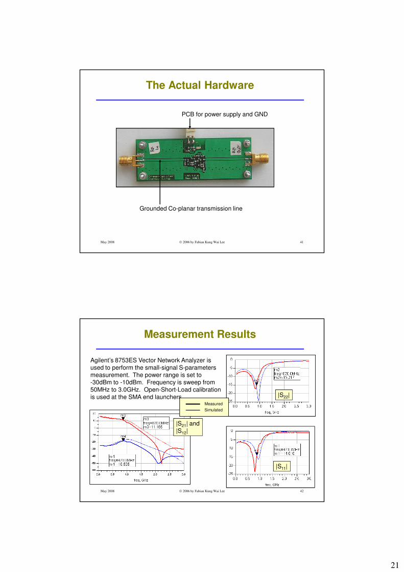
May 2008 2006 by Fabian Kung Wai Lee 41
The Actual Hardware
Grounded Co-planar transmission line
PCB for power supply and GND
May 2008 2006 by Fabian Kung Wai Lee 42
Measurement Results
|S11|
|S22|
|S21| and
|S12|
Agilent’s 8753ES Vector Network Analyzer is
used to perform the small-signal S-parameters
measurement. The power range is set to
-30dBm to -10dBm. Frequency is sweep from
50MHz to 3.0GHz. Open-Short-Load calibration
is used at the SMA end launchers.Measured
Simulated

22
May 2008 2006 by Fabian Kung Wai Lee 43
Appendix 1 – Monolithic Microwave
Integrated Circuit (MMIC) Amplifier
May 2008 2006 by Fabian Kung Wai Lee 44
Monolithic Microwave Integrated
Circuit (MMIC)
• Nowadays you can easily built an RF amplifier using MMIC amplifier
module.
• These usually contain a Darlington transistor pair with series and shunt
feedbacks. The feedback serve to increase the bandwidth of the
amplifier and internally match the input and output impedance to 50Ω.
• For example see Avago Technologies’ MSA series devices datasheet.
Port
Output
Num=2
Port
Input
Num=1
R
R2
R
R3
Port
P4
Num=4
Port
P3
Num=3
R
R1
BJT_NPN
BJT2
BJT_NPN
BJT1
Example of MMIC amplifier
schematic
Series
feedback
Shunt
feedback