1004 ieee journal of solid-state circuits, vol. 40, no. 4
TRANSCRIPT
1004 IEEE JOURNAL OF SOLID-STATE CIRCUITS, VOL. 40, NO. 4, APRIL 2005
A 20-Gb/s 0.13-�m CMOS Serial Link TransmitterUsing an LC-PLL to Directly Drive the
Output MultiplexerPatrick Chiang, Student Member, IEEE, William J. Dally, Fellow, IEEE, Ming-Ju Edward Lee, Member, IEEE,
Ramesh Senthinathan, Senior Member, IEEE, Yangjin Oh, and Mark A. Horowitz, Fellow, IEEE
Abstract—A 20-Gb/s transmitter is implemented in 0.13- mCMOS technology. An on-die 10-GHz LC oscillator phase-lockedloop (PLL) creates two sinusoidal 10-GHz complementary clockphases as well as eight 2.5-GHz interleaved feedback divider clockphases. After a 2
201 pseudorandom bit sequence generator
(PRBS) creates eight 2.5-Gb/s data streams, the eight 2.5-GHzinterleaved clocks 4:1 multiplex the eight 2.5-Gb/s data streamsto two 10-Gb/s data streams. 10-GHz analog sample-and-holdcircuits retime the two 10-Gb/s data streams to be in phase withthe 10-GHz complementary clocks. Two-tap equalization of the10-Gb/s data streams compensate for bandwidth rolloff of the10-Gb/s data outputs at the 10-GHz analog latches. A final 20-Gb/s2:1 output multiplexer, clocked by the complementary 10-GHzclock phases, creates 20-Gb/s data from the two retimed 10-Gb/sdata streams. The LC-VCO is integrated with the output mul-tiplexer and analog latches, resonating the load and eliminatingthe need for clock buffers, reducing power supply induced jitterand static phase mismatch. Power, active die area, and jitter(rms/pk-pk) are 165 mW, 650 m 350 m, and 2.37 ps/15 ps,respectively.
Index Terms—High-speed I/O, oscillators, multiplexing,OC-192, phase-locked loops, sample and hold circuits, transmit-ters.
I. INTRODUCTION
NEW DEVELOPMENTS in high-speed serial links havebeen crucial in scaling off-chip system bandwidth with
CMOS on-chip bandwidth. Bandwidth/pin must continue to in-crease, as CMOS scaling steadily increases the bandwidth/mmon-die. As these data rates increase, the importance of timingprecision in link performance becomes one of the dominant fac-tors in the ability to scale off-chip with on-chip bandwidth.
Previously, many serial link designs have used multiphasephase-locked loops (PLLs), using multiphase multiplexing, toachieve fast bandwidth/pin performance [1], [2]. As data ratesincrease, and timing uncertainty becomes the critical bottleneck
Manuscript received September 3, 2004; revised December 3, 2004. Thiswork was supported by grants from Intel Corporation, MARCO, and Cray.
P. Chiang, Y. Oh, and M. A. Horowitz are with the Computer SystemsLaboratory, Stanford University, Stanford, CA 94305 USA (e-mail: [email protected]).
W. J. Dally is with Stream Processors, Inc., Sunnyvale, CA 94085 USA, andalso with the Computer Systems Laboratory, Stanford University, Stanford, CA94305 USA.
M.-J. E. Lee is with ATI Technologies Systems Corporation, Inc., ATI Re-search Silicon Valley Inc., Santa Clara, CA 95054 USA.
R. Senthinathan is with ATI Technologies, Inc., Markham, ON L3T 7X6,Canada.
Digital Object Identifier 10.1109/JSSC.2004.842841
in link performance, these links suffer reduced timing marginfor a few reasons. One problem is the difficulty in maintainingphase symmetry between the multiple phases. For example,threshold mismatches and capacitive layout mismatches in thetiming vernier may cause static phase errors and unequal eyeopenings. Various techniques have been proposed to alleviatethis static phase offset problem [3]–[5], but they suffer fromlarge area overhead as well as residual static phase offset fromquantization error.
A second problem is that conventional serial links use a se-ries of post-PLL clock buffers, in order to increase the clockfanout for the transmitter multiplexing. As these buffers lie out-side of the PLL, their jitter is not reduced by the PLL feed-back loop, resulting in a significant source of high frequencyclock jitter, such as through a noisy supply voltage. Varioustechniques have been proposed to alleviate buffer sensitivity [2],[6], but the need for high fanout due to large transmitter multi-plexing (muxing) capacitances results in large power dissipationfor these techniques.
As a result, some current CMOS serial link transmitters of10 Gb/s retime the data at the full rate of 10 GHz [7], [8]. Whilethis mitigates the phase symmetry and jitter issues, full rate ar-chitectures also increase power, area, and circuit complexity,as the on-die circuitry bandwidth is the same as the off-chipbandwidth.
In this paper, we describe a 20-Gb/s transmitter implementedin 0.13- m CMOS, where the final 2:1 output multiplexer/drivercapacitance is subsumed directly into the complementary nodesof the 10-GHz LC-VCO, alleviating many of the aforemen-tioned problems. First, the complementary nodes of the high-LC resonator obey low static phase offset, resulting in sym-metric eye openings. Second, by driving the final 2:1 outputdriver directly by the complementary sinusoidal phases of a10-GHz LC-VCO, the output data jitter depends solely on theLC-PLL jitter, as the post-PLL buffers are no longer necessary.Finally, as only the final 2:1 output multiplexer is running at the20-Gb/s line rate, this architecture achieves low area, power, andcircuit complexity.
The following is the outline for the rest of this paper. Sec-tion II briefly describes the overall transmitter architecture.Section III discusses in detail the performance of the LC-VCO,delving into the power supply sensitivity and residual staticphase offset. Section IV discusses the PLL. Section V describesthe transmitter muxing circuitry to achieve 20-Gb/s data rate.Section VI shows the experimental results.
0018-9200/$20.00 © 2005 IEEE

CHIANG et al.: A 20-Gb/s 0.13- m CMOS SERIAL LINK TRANSMITTER USING AN LC-PLL TO DIRECTLY DRIVE THE OUTPUT MULTIPLEXER 1005
Fig. 1. Transmitter architecture.
II. SYSTEM ARCHITECTURE
Fig. 1 shows the complete transmitter architecture. A 20 bit,pseudorandom bit sequence (PRBS) generator , cre-ates an eight-bit-wide data stream at 2.5 GHz. These eight datastreams are retimed and sent to two sets of 4:1 multiplexers, cre-ating two 10-Gb/s data streams offset in phase by 50 ps. The two10-Gb/s data streams are retimed to the 10-GHz clock domainby two analog sample-and-hold circuits. The final 2:1 outputbuffer multiplexes the two 10-GHz data streams to 20 Gb/s. Thisarchitecture allows for the final transmitter jitter generation todepend solely on the jitter of the complementary 10-GHz clock(CLK and CLKb).
Notice that a significant amount of delay exists betweenthe 16 2.5-GHz clock phases and the complementary 10-GHzphases, making it difficult to ensure valid setup/hold time ofthe two 10-Gb/s data streams in relation to the 10-GHz com-plementary clocks. Each of the clock phases suffers from largedelay variance, as the phases pass through low-to-high levelconversion, interpolator stages, and fanout buffering beforearriving at the 4:1 10-Gb/s multiplexer. Hence, a 5-bit DACphase interpolator is needed to adjust each of the sixteen phases.Coarse interpolation is achieved using tri-state buffer currentsumming, while fine interpolation is done through capacitivetrimming, resulting in a minimum interpolation step of 8 psand a maximum step of 50 ps. Calibration logic to adjust the16 2.5-GHz phases in relation to the 10-GHz complementaryclocks was not implemented on this chip, and therefore, timingmargin is achieved off-line by adjusting the interpolator stepsthrough a scan chain.
III. LC-VCO
The transmitter output jitter/skew is limited by the intrinsicjitter/skew of the clocks generated by the phase-locked loop.Any additional buffer stages between the PLL (point of gen-eration) and the transmitter muxing (point of use) add addi-tional jitter/skew to the nominal jitter/skew of the PLL. Qual-itatively, this can be seen in Fig. 2. As the number of bufferstages in the clock buffer chain increases, static phase offsetand power supply induced jitter increase. Static phase offsetincreases as more devices exist in the clock chain, increasing
Fig. 2. Relationship between clock buffering and increased static phaseoffset/power supply induced jitter.
the probability for more threshold voltage mismatch and capac-itance layout mismatch, resulting in timing skew between mul-tiphase clocks. Likewise, each additional buffer adds additionalpower supply sensitivity, resulting in larger timing jitter as aresult of power supply noise. At the limit, using the architec-ture implemented in this paper, no buffers are used between thevoltage-controlled oscillator (VCO) (point of generation) andthe transmitter muxing (point of use), leaving only the residualpower supply sensitivity/static phase skew of the intrinsic VCOitself. The next section will describe the implemented VCO andthe residual power supply sensitivtity/static phase skew of theVCO.
Fig. 3(a) shows the implemented LC-VCO, consisting of aspiral inductor placed across the complementary nodes of cross-coupled inverters. The 0.5-nH differential spiral is fabricatedusing top level metal (metal eight), and has a simulated (usingASITIC [9]) of 11.8 and 10.4, with and without ground shield,respectively. This small difference in is due to the inherentlow doped substrate, as well as the large distance (5.6 m) ofseparation between metal eight and the substrate.
Using an LC-based VCO has several advantages. First, a10-GHz oscillation frequency would be difficult to achieve,with any significant fanout, using a ring oscillator, or wouldrequire a prohibitively large amount of power. For example, athree-stage 10-GHz current-mode logic (CML) ring oscillatorwas simulated in HSPICE, burning 40 mW, versus 5 mW fora LC-VCO.
Second, subsuming the output multiplexer capacitance di-rectly into the resonator removes any post-PLL clock buffers,

1006 IEEE JOURNAL OF SOLID-STATE CIRCUITS, VOL. 40, NO. 4, APRIL 2005
Fig. 3. (a) LC-VCO schematic. (b) Resonator Q with/without poly gateresistance.
which are a significant source of high-frequency jitter. Themeasured supply sensitivity (fraction delay change per frac-tion of supply change [2], [7]) of the LC-VCO was measuredby applying a 10-ps rise time, 10% noise voltage on the supply,resulting in 0.11 (transient phase step) and 0.01 (steady-statephase error). These numbers are comparable to a supply regu-lated delay line [2] and power supply compensated buffer [7],but only dissipates 5 mW while driving a large fanout of 1 pF,at a cost of larger inductor area. Higher rejection of powersupply noise can be achieved with smaller devices and higheroscillator , while incurring the penalty of larger inductorarea.
Third, subsuming the load capacitance directly into the LCtank and resonating the capacitance significantly decreases thepower dissipated. For example, simulation of two stages of in-verters driving the clock loading capacitance burns an additional10 mW.
One possible problem might concern resonator degradationdue to the many sources of capacitances that sum to the totalresonator capacitance. Half of the tank capacitance is domi-nated by high- varactor capacitance (460 ff), while passivewiring capacitance makes up another quarter of total capaci-tance, leaving approximately 270 ff of NMOS gate capacitance.Careful layout to reduce any parasitic resistances, such as S/Dseries resistance and gate resistance, is crucial towards mini-mizing resonator loss. For example, the varactor uses 32 parallelfingers of 6 m/0.36 m, strapped on both sides of the transistor.Even with special care, the series gate poly resistance dominatesresonator loss; series gate resistance is 1.5 , causing a degra-dation of 17%, seen in Fig. 3(b).
Fig. 4. (a) Rise/fall asymmetry due to �50-mV PMOS threshold voltagemismatch. (b) Voltage mismatch/asymmetry due to 5% capacitance mismatchbetween resonator nodes.
Another possible problem might arise from long wiringtraces between the VCO and various blocks. One particularroute, from the LC-VCO to the frequency divider, is unusuallylong (300 m), with 20 ff of the frequency divider gate capac-itance at the end. ASITIC parasitic extraction showed that thisM8 thick metal (300 m 4 m) at 10 GHz is observed asa 0.1-nH 0.2- 20-ff transmission line. Transient simulationshows a phase lag at the divider of 1 ps, and a degradationof 1% from this long wiring trace. Next, the residual staticphase offset of the VCO is described.
There are two potential problems that can affect the staticphase offset of both resonator outputs. First, transistor mismatchsuch as threshold mismatch causes second-order distortion thatdistorts the sinusoids and creates asymmetry in the rise and falltime. This has minimal effect on the zero crossings of the clocksignals but affects the sinusoidal symmetry, which can causeunequal eye openings. This asymmetry is attenuated by the large
of the resonator, as the larger increases signal amplitude,minimizing the effect of threshold mismatch. For example, asseen in Fig. 4(a), when one PMOS of the cross coupled pairhas a 50-mV threshold mismatch, the rise time slope is largerthan the fall time, due to the improved of the PMOS devicewith the smaller threshold voltage. However, the resulting staticphase error is still 1 ps.
Second, capacitance mismatch of both resonator nodes alsohas an effect on waveform symmetry and possibly static phaseoffset. A capacitance difference between complementary out-puts acts as a capacitive divider between the two nodes. As well,a rise and fall time asymmetry will occur, due to the asymmetriccurrent charging/discharging of different capacitances. Boththe voltage difference and rise/fall timing asymmetry causestatic phase offset and uneven zero crossings. By increasing thedrive strength of the inverters, the capacitive-dependentvoltage is mitigated, as the complementary nodes becomevoltage limited by the supply. As well, improving the resonator
also minimizes the effect of capacitance mismatch as thethreshold voltage mismatch is mitigated by larger voltageswings. Fig. 4(b) illustrates a simulation with 50-mV transistor

CHIANG et al.: A 20-Gb/s 0.13- m CMOS SERIAL LINK TRANSMITTER USING AN LC-PLL TO DIRECTLY DRIVE THE OUTPUT MULTIPLEXER 1007
Fig. 5. 10-GHz PLL.
mismatch and 5% capacitance mismatch, exhibiting voltageamplitude mismatch 4%, and static phase offset 2 ps.
IV. PHASE-LOCKED LOOP (PLL)
The block diagram for the PLL is seen in Fig. 5. A 1.25-GHzoff-chip clock is sent to a linear phase comparator, a conven-tional charge pump, and two-pole loop filter. An unsilicidedpoly resistor is used for the loop filter zero, and the two filtercapacitors use NMOS gate capacitance to achieve high capac-itive density. The LC-VCO generates 10-GHz complementaryclocks, which are divided by a 4:1 CML divider. The output isfurther divided by a digital 2:1 divider in order to run the phasecomparator and charge pump at a lower frequency of 1.25 GHz.
A PMOS source follower, using the thick oxide transistors, isused as a level shifter between the charge pump loop filterand the actual VCO varactor control . This has two ad-vantages. One is that the loop filter voltage is more isolated fromthe VCO, reducing phase noise enhancement from nonlinear ef-fects, such as large-signal AM modulation. For example, var-actor control voltage ripple is reduced 3 from 230 mV to75 mV. Second, gain reduction in the source follower increasesthe varactor voltage dynamic range. Since the source followerconverts the 1.2-V charge pump voltage into the 3.3-V voltagedomain, it allows for larger varactor bias dynamic range andtherefore, increased tuning range.
V. TRANSMITTER MULTIPLEXING
The transmitter 8:1 muxing starts with a 20-bitPRBS, creating eight parallel 2.5-Gb/s data streams as inFig. 6(a). These eight data streams are 4:1 multiplexed into two2-tap equalized 10-Gb/s data streams, using the 16 interpolatedclocks from the PLL. The two 10-Gb/s data streams are retimedto the clock domain of the 10-GHz LC-VCO clock by the use of10-GHz analog latches. The two 10-Gb/s retimed data streamsare then sent to the final 2:1 output multiplexer, achieving20-Gb/s data rate at the differential output.
A. 4:1 10-Gb/s Multiplexer
Sixteen 2.5-GHz clock phases create two 10-Gb/s datastreams using a 4:1 output multiplexing scheme. Fig. 6(b)shows one of the 10-Gb/s multiplexing paths, using four
Fig. 6. (a) Transmitter muxing block diagram. (b) 4:1 10-Gb/s multiplexer.(c) 4:1 10-Gb/s multiplexer with 2-tap equalization.
2.5-GHz phases. Notice that both the rising and falling edges ofa single clock are separated into two clock phases; for example,
and are two separate clocks. It is possibleto use only four clock phases for each 4:1 multiplexer, butbecause a phase interpolator adjusts the phases for the 4:1multiplexing stage, additional design complexity exists whenthe rising/falling edges of an interpolated clock need to beadjusted independently of each other.
Alternatively, the use of a two-stage NMOS pulldown multi-plexer can be achieved using a dynamic AND structure, whichmerges the clock phase with the data [10], as opposed to theimplemented three-stack NMOS multiplexer. However, such ascheme adds two stages of transistors between the clock signaland the multiplexer, allowing for possible static timing mis-match at the multiplexer that cannot be accounted for by thepreceding phase interpolator. Using a three-stage NMOS pull-down multiplexer ensures that if the eight interpolated multi-phases are aligned with the two 10-GHz complementary clockphases, timing closure can be insured.
While the implemented three-stage NMOS pulldown mul-tiplexer minimizes the possible static phase offset problem,gain/bandwidth of the multiplexer becomes an issue. Also,aperture time/bandwidth limitations of the proceeding 10-GHzanalog latch increases intersymbol interference (ISI), translatingto ISI at the final 20-Gb/s output eye. Two-tap equalization isemployed to relax the bandwidth constraints, by equalizing the

1008 IEEE JOURNAL OF SOLID-STATE CIRCUITS, VOL. 40, NO. 4, APRIL 2005
Fig. 7. 10-GHz analog latch.
low-pass channel characteristics. Fig. 6(c) shows the currentsumming at the output of the 10-Gb/s data streams, using a de-layed version of the data to achieve 10-Gb/s 2-tap equalization.The benefits of this equalization will be described in the nextsection.
B. 10-GHz Analog Latch
Fig. 7 shows the schematic of the 10-GHz analog latch used.As the complementary 10-GHz clocks CLKb and CLK fall,the differential signal InData0 is sampled onto the intermediatenode OutData0. Full pass gates are used to mitigate charge in-jection loss onto the sampled nodes. Other types of high-speedanalog latches were deemed less effective. For example, a pass-gate analog sampler is ineffective, as a large (400–600 mV)voltage swing is sampled onto node OutData0. A CML latchis another alternative, but it has reduced aperture time for largedifferential voltage swings, as charge sharing through the dif-ferential pair occurs when the clock is sampled and the currentis not immediately switched off.
While the aperture time is very fast at the output nodesfor the implemented latch, significant hysteresis exists. Sinceonly two-phase 10-GHz clocking exists, one phase of clock isused for sampling and the other for holding; no clock phaseexists to reset the sampled nodes and remove the hysteresis.However, hysteresis can be observed as bandwidth reduction,or ISI, and compensated for using the preceding 10-Gb/s 2-tapequalization. Fig. 8 illustrates the sampled differential analoglatch voltage (OutData0) with and without pre-emphasis.When pre-emphasis of OutData0 is turned off, significant ISIis observed for three post-cursor bit periods when the “010”data stream is transmitted. When pre-emphasis is enabled,the latched differential voltage remains constant over thatsame transmitted bit sequence. Fig. 9 also shows the utility ofpre-emphasis of the analog latch. Note that the dotted line isfor voltage waveforms with equalization and the solid line forwaveforms without equalization. Fig. 9 (Panel 4) shows theanalog latch input with and without pre-emphasis. The output ofthe latch in Fig. 9 (Panel 7) shows the latched analog 10-Gb/sdata streams, with significant ISI at fast edge transitions.Fig. 9 (Panel 12) shows the 20-Gb/s transmitter output withand without equalization of the analog latches. A significantamount of eye closure (15%) is observed in the 20-Gb/s outputeye for the nonequalized latch (solid line) as compared to theequalized case (dotted line).
Fig. 8. Simulated 10-GHz analog latch outputs without/with equalization.
Fig. 9. Panel 4) Simulated inputs to 10-GHz analog latch with/withoutequalization. Panel 7) Simulated output of 10-GHz analog latch with/withoutequalization. Panel 12) Simulated output of 20-Gb/s 2:1 output multiplexer.
C. Final 20-Gb/s 2:1 Output Multiplexer
The retimed 10-Gb/s data streams are multiplexed by the final2:1 output driver, shown in Fig. 10. The 2:1 output driver isimplemented using source coupled pairs, current summing onboth differential pairs through 50- on-die poly terminationresistors.
One issue of concern with this merged VCO/output driverdesign is the possibility of data-dependent voltage noise/kick-back, degrading VCO phase noise. This problem can arise fromdata-dependent modulation of the differential pair tail voltage,causing charge variation/kickback through , ultimately af-fecting resonator tank capacitance and oscillation frequency.This data-dependent kickback into the LC-VCO was simulatedin HSPICE by changing one of the inputs of the 2:1 multi-plexer dynamically, causing the 20-Gb/s output data to toggle.The period of the VCO is measured before and after the dy-namic data change, with the observed VCO period changing lessthan 0.2 ps. This small VCO perturbation can be attributed tothe ability of the differential pair tail node to maintain a virtual

CHIANG et al.: A 20-Gb/s 0.13- m CMOS SERIAL LINK TRANSMITTER USING AN LC-PLL TO DIRECTLY DRIVE THE OUTPUT MULTIPLEXER 1009
Fig. 10. Final 20-Gb/s 2:1 output multiplexer.
Fig. 11. Die photograph.
ground. Simulation shows only a 40-mV tail node voltage mod-ulation associated with the output voltage change, resulting inan insignificant amount of charge to perturb the VCO resonator.
VI. EXPERIMENTAL RESULTS
Fig. 11 shows the die photograph. Including the bondingpads, the die area is 700 m 1100 m. The two arrays ofinner pads along the top and bottom of the die allow for on-die,high bandwidth 50- termination impedance using CascadeMicrotech probes. The 20-Gb/s differential data stream travelsthrough the on-die high bandwidth probes, through two setsof dc blocking connectors, one meter of coax, and into theoscilloscope input. Total insertion loss is 3.6 dB at 10 GHz,exhibiting some amount of frequency-dependent attenuation.
Fig. 12(a) shows the spectrum analyzer output of a 2.5-GHzdivide-by-4 clock from the standalone PLL, locked at 9.6 GHz.The measured 3-dB bandwidth of the locked PLL is 13 MHz.There is bandwidth peaking of around 3.6 dB in the PLL. Dueto an inappropriately sized loop filter resistor, the damping isless than 0.5. The phase noise at 1-MHz offset is 99.7 dBc/Hzobserved in the presence of a large noise floor, and 120 dBc/Hzbeyond 100 MHz.
The standalone PLL jitter was measured using an HP54754Aoscilloscope, and an Agilent 8133A waveform generator. Thejitter of a 1.25-GHz clock source from the 8133A was 1.13 ps(RMS), 8.9 ps (pk-pk). Fig. 12(b) shows that the jitter histogramof the 10-GHz clock output is 0.97 ps (rms), 8 ps (pk-pk). Sincethe PLL bandwidth of 13 MHz is relatively high, much of the
Fig. 12. (a) Power spectrum of 2.5 Hz divided clock from the 10-GHz PLL.(b) 10-GHz clock jitter histogram.
Fig. 13. 20-Gb/s eye diagram.
PLL output jitter is passed directly from the 8133A input refer-ence. This suggests that a quieter input reference is needed toascertain the true performance of the 10-GHz PLL. The mea-sured integrated jitter (50 kHz–80 MHz) was 4 mUI (rms).
Fig. 13 shows the eye diagram, at a data rate of 19.2 Gb/s.The outputs are superimposed on each other. The eye openingamplitude is approximately 105 mV at the oscilloscope input.The measured jitter is 2.37 ps (rms) and 15.6 ps (pk-pk). Mea-sured static phase offset between eight consecutive bits is less
1010 IEEE JOURNAL OF SOLID-STATE CIRCUITS, VOL. 40, NO. 4, APRIL 2005
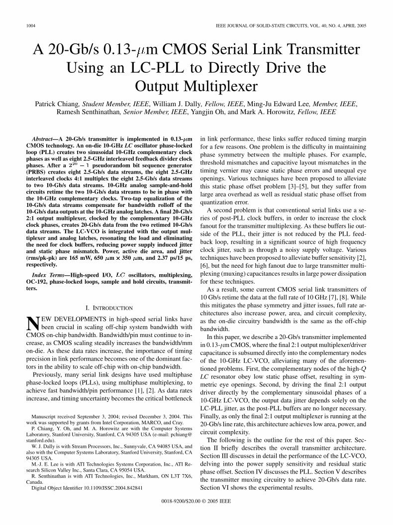
TABLE IMEASURED JITTER OF 2.5-GHZ PLL CLOCK WITH VARIOUS CONFIGURATIONS
than 2 ps. Notice that there is a 60-mV voltage ripple seen at thebottom of the eye, also predicted from simulation. This phenom-enon occurs during the transition period of the sinusoidal com-plementary clocks, when neither tail NMOS is fully on, and thedifferential pair no longer acts with a constant bias current. In-stead, the current drops during the transitions, causing the outputnodes to pull up to the supply during the zero crossings of theclocks.
The transmitter works from 16.32–19.2 Gb/s, slower thanour initial specification of 20 Gb/s. This was actually ob-served in parasitic extraction simulation, showing the trans-mitter working from 16.8–19.6 Gb/s. The cause of this isexcessive capacitive loading of the complementary resonatorclock nodes, with wide top thick metal (300 m 4 m) con-necting the frequency divider and the final 2:1 output multi-plexer. More careful floorplanning of the layout would haveplaced the divider closer to the output multiplexer, reducingthis clock loading. Increasing PLL tuning range, such as usingswitch capacitor banks for the tank resonator, can also helpalleviate this potential problem.
We attempted to determine the effect of data-dependentkickback on PLL jitter accumulation by measuring the trans-mitter in various configurations. This was done by measuringthe 2.5-GHz divided clock coming from the PLL itself. Ifpoor isolation exists between the transmitter VCO and thetransmitter latches/muxes, we would expect the 2.5-GHz PLLclock to have the largest jitter when PRBS data is transmitted.Table I illustrates the results of our measurements. When onlythe PLL is enabled, with the PRBS and the transmitter muxingdisabled, the measured jitter is 1.25 ps, 10 ps (rms, pk-pk).With the PLL and transmitter muxing on (sending all zeroes)and the PRBS off, the jitter is 1.25 ps, 8.9 ps (rms, pk-pk),illustrating no change in jitter. With the same configuration,while sending a lone one, the jitter again does not change, withthe measured jitter at 1.21 ps, 10 ps (rms, pk-pk). The jitter ofthe 2.5-GHz clock increases substantially (2.3 ps, 16.7 ps) whenthe transmitter is turned off, but the PLL and PRBS are bothon. This illustrates that the dominant source for the increasedjitter is the power supply noise, either/both in the divide-by-4or the buffer chain to the output pin. Finally, when the PLL,PRBS, and the transmitter are on, sending random 20-Gb/sdata at the output, the measured jitter is 2.25 ps, 15.6 ps. Sincethis measured jitter is roughly the same as the situation withthe PRBS on and transmitter off, we can infer that the increasein measured jitter is dominated by digital power supply jitter
caused by the PRBS. Measured results using the a spectrumanalyzer do not uncover any other conclusions. While theseresults do not imply that data-dependent jitter does not increasePLL jitter accumulation, the results clearly suggest that suchdata-dependent accumulation is less significant than digitalpower supply noise.
VII. CONCLUSION
A 20-Gb/s serial link was designed in a 0.13- m CMOSprocess. The final transmitter output multiplexer is clockeddirectly by the two complementary phases of the LC resonatorin the 10-GHz PLL. This allows most of the transmitter to runat the half rate of 10 Gb/s, decreasing the area, power con-sumption, and complexity in respect to full-rate architectures.In addition, subsuming the output mux capacitance into theresonator removes PLL clock buffering, a significant sourceof high frequency jitter. Finally, due to the inherent symmetryof a LC voltage controlled oscillator, both complementaryphases exhibit little static phase offset, resulting in symmetriceye openings. The 20-Gb/s transmitter dissipates 165 mW in650 m 350 m. As conventional link channels are unlikelyto achieve flat frequency response through 10-GHz bandwidth,future work includes increasing output drive strength andimplementing transmitter pre-emphasis to combat intersymbolinterference.
ACKNOWLEDGMENT
The authors would like to thank J. Poulton, K. Mai, and J. Kimfor helpful discussions, and M. Kellam, R. Palmer, and H.-T. Ngfor fabrication support, Prof. T. Lee for testing equipment, andP. Prather for bond wire expertise.
REFERENCES
[1] C.-K. Yang and M. Horowitz, “A 0.8 �m CMOS 2.5 Gb/s oversamplingreceiver and transmitter for serial links,” IEEE J. Solid-State Circuits,vol. 31, no. 12, pp. 2015–2023, Dec. 1996.
[2] M.-J. E. Lee, W. J. Dally, and P. Chiang, “Low-power area-efficient high-speed I/O circuit techniques,” IEEE J. Solid-State Circuits, vol. 35, no.11, pp. 1591–1599, Nov. 2000.
[3] L. Wu and W. C. Black Jr., “A low-jitter skew-calibrated multiphaseclock generator for time-interleaved applications,” in IEEE Int. Solid-State Circuits Conf. (ISSCC) Dig. Tech. Papers, Feb. 2001, pp. 396–397.
[4] C.-H. Park, O. Kim, and B. Kim, “A 1.8-GHz self-calibrated phase-locked loop with precise I/Q matching,” IEEE J. Solid-State Circuits,vol. 36, no. 5, pp. 777–783, May 2001.
[5] R. Farjad-Rad et al., “0.622–8.0 Gb ps 150 mW Serial IO macrocell withfully flexible preemphasis and equalization,” in Symp. VLSI Circuits Dig.Tech. Papers, June 2003, pp. 63–66.
[6] M. Mansuri and C.-K. Ken Yang, “A low-power low-jitter adaptive-bandwidth PLL and clock buffer,” in IEEE Int. Solid-State Circuits Conf.(ISSCC) Dig. Tech. Papers, vol. 1, Feb. 2003, pp. 430–505.
[7] J. Cao et al., “OC-192 transmitter and receiver in standard 0.18-/splmu/m CMOS,” IEEE J. Solid-State Circuits, vol. 37, no. 12, pp.1768–1780, Dec. 2002.
[8] L. Henrickson et al., “Low-power fully integrated 10-Gb/s SONET/SDHtransceiver in 0.13-�m CMOS,” IEEE J. Solid-State Circuits, vol. 38, no.10, pp. 1595–1601, Oct. 2003.
[9] A. M. Niknejad, “Modeling of passive elements with ASITIC,” in Proc.IEEE Radio Frequency Integrated Circuits (RFIC) Symp., June 2002,pp. 303–306.
[10] W. Ellersick et al., “A serial-link transceiver based on 8 Gsample/s A/Dand D/A converters in 0.25�m CMOS,” in IEEE Int. Solid-State CircuitsConf. (ISSCC) Dig. Tech. Papers, Feb. 2003, pp. 58–59.
CHIANG et al.: A 20-Gb/s 0.13- m CMOS SERIAL LINK TRANSMITTER USING AN LC-PLL TO DIRECTLY DRIVE THE OUTPUT MULTIPLEXER 1011
Patrick Chiang (S’99) received the B.S. degree inelectrical engineering and computer sciences fromthe University of California at Berkeley in 1997,and the M.S. degree in electrical engineering fromStanford University, Stanford, CA, in 2001. He iscurrently working toward the Ph.D. degree in theComputer Systems Laboratory, Stanford University.
In 1998, he was with Datapath Systems (nowLSI Logic), working on analog front-ends for DSLchipsets. In 2004, he was a consultant at TelegentSystems, Sunnyvale, CA, working on various
mixed-signal RF circuits. His interests are in ultra-wideband RF architectures,high-speed serial links, and circuit design for biological systems.
William J. Dally (M’80–SM’01–F’02) received theB.S. degree in electrical engineering from the Vir-ginia Polytechnic Institute, Blacksburg, the M.S. de-gree in electrical engineering from Stanford Univer-sity, Stanford, CA, and the Ph.D. degree in computerscience from the California Institute of Technology(Caltech), Pasadena.
He is the Willard R. and Inez Kerr Bell Professorof Engineering and the Chair of the Departmentof Computer Science at Stanford University. Heand his group have developed system architecture,
network architecture, signaling, routing, and synchronization technology thatcan be found in most large parallel computers today. While at Bell TelephoneLaboratories, he contributed to the design of the BELLMAC32 microprocessorand designed the MARS hardware accelerator. At Caltech, he designed theMOSSIM Simulation Engine and the Torus Routing Chip which pioneeredwormhole routing and virtual-channel flow control. While a Professor ofElectrical Engineering and Computer Science at the Massachusetts Institute ofTechnology, his group built the J-Machine and the M-Machine, experimentalparallel computer systems that pioneered the separation of mechanisms fromprogramming models and demonstrated very low overhead synchronizationand communication mechanisms. At Stanford University, his group hasdeveloped the Imagine processor, which introduced the concepts of streamprocessing and partitioned register organizations. He has worked with CrayResearch and Intel to incorporate many of these innovations in commer-cial parallel computers, with Avici Systems to incorporate this technologyinto Internet routers, co-founded Velio Communications to commercializehigh-speed signaling technology, and co-founded Stream Processors, Inc. tocommercialize stream processor technology. He currently leads projects onhigh-speed signaling, computer architecture, and network architecture. He haspublished over 150 papers in these areas and is an author of the textbooksDigital Systems Engineering (Cambridge, U.K.: Cambridge University Press,1998) and Principles and Practices of Interconnection Networks (San Mateo,CA: Morgan Kaufmann, 2003).
Dr. Dally is a Fellow of the Association for Computing Machinery (ACM)and has received numerous honors including the IEEE Seymour Cray Awardand the ACM Maurice Wilkes award.
Ming-Ju Edward Lee (S’98–M’01) received theB.S. degree in electrical engineering and com-puter sciences from the University of California atBerkeley in 1997, and the M.S. and Ph.D. degreesin electrical engineering from Stanford University,Stanford, CA, in 2000 and 2001, respectively.
He is currently an Engineering Manager of circuitdesign with ATI Research Silicon Valley, Santa Clara,CA. From 2000 to 2003, he was with Velio Commu-nications Inc., where he led a 6.25-Gb/s serial I/O de-velopment.
Ramesh Senthinathan (S’82–M’86–SM’04) re-ceived the B.S. degree in computer engineeringfrom the State University of New York at Buffalo in1984, and the M.S. and Ph.D. degrees in electricalengineering from the University of Arizona, Tucson,in 1986 and 1992, respectively.
He is currently a Director of Engineering respon-sible for I/O, analog, and technology developmentwith ATI Technologies, Santa Clara, CA. He was aDirector of Engineering with Velio Communications,Milpitas, CA, responsible for both technology and
product development from 2001 to 2003. From 1995 to 2001, he was with IntelCorporation as a Director and Distinguished Engineer for Communication andMicroprocessor groups in Sacramento and Folsom, CA. He was responsible forall aspects of circuit design of Pentium Pro (Desktop and Server) and PentiumIII microprocessor design. With Level One acquisition, he moved to the IntelCommunication group, and managed Analog Front End group for Intel’s DSLdivision. From 1993 to 1995, he was with Motorola, Inc. as a Principal Engi-neer responsible for 16/24 bit DSP analog and I/O circuit designs. He was aStaff Engineer with IBM Research from 1992 to 1993. From 1986 to 1989, hewas a Design Engineer with the ASIC and Microcontroller groups at Intel Cor-poration, Chandler, AZ. He has published more than 50 refereed papers in theseareas, and is a coauthor of the book Simultaneous Switching Noise of CMOSDevices and Systems (New York: Springer, 1993).
Yangjin Oh received the B.S. degree from SeoulNational University, Seoul, Korea, in 2000 and theM.S. degree in electrical engineering from StanfordUniversity, Stanford, CA, in 2002. He is currentlyworking toward the Ph.D. degree at Stanford Uni-versity.
He interned as a Circuit Design Engineer at Na-tional Semiconductor, Santa Clara, CA, during thesummer of 2002. His research interests include signalprocessing and mixed-signal circuit design in wire-less communication.
Mark A. Horowitz (S’77–M’78–SM’95–F’00)received the B.S. and M.S. degrees in electricalengineering from the Massachusetts Institute ofTechnology, Cambridge, in 1978, and the Ph.D.degree from Stanford University, Stanford, CA, in1984.
He is the Yahoo Founder’s Professor of ElectricalEngineering and Computer Science at StanfordUniversity. His research area is in digital systemdesign, and he has led a number of processor designsincluding MIPS-X, one of the first processors to in-
clude an on-chip instruction cache, TORCH, a statically scheduled, superscalarprocessor that supported speculative execution, and FLASH, a flexible DSMmachine. He has also worked in a number of other chip design areas includinghigh-speed and low-power memory design, high-bandwidth interfaces, andfast floating point. In 1990 he took leave from Stanford to help start RambusInc., Los Altos, CA, a company designing high-bandwidth chip interfacetechnology. His current research includes multiprocessor design, low powercircuits, memory design, and high-speed links.
Dr. Horowitz received the Presidential Young Investigator Award and an IBMFaculty development award in 1985. In 1993, he received the Best Paper Awardat the IEEE International Solid-State Circuits Conference.