10ecl78-power electronics lab 2017-18 lab.pdf · 10ecl78-power electronics lab 2017-18 ... to...
TRANSCRIPT
10ECL78-Power Electronics Lab 2017-18
Dept. of ECE, CIT, Gubbi Page No. 1
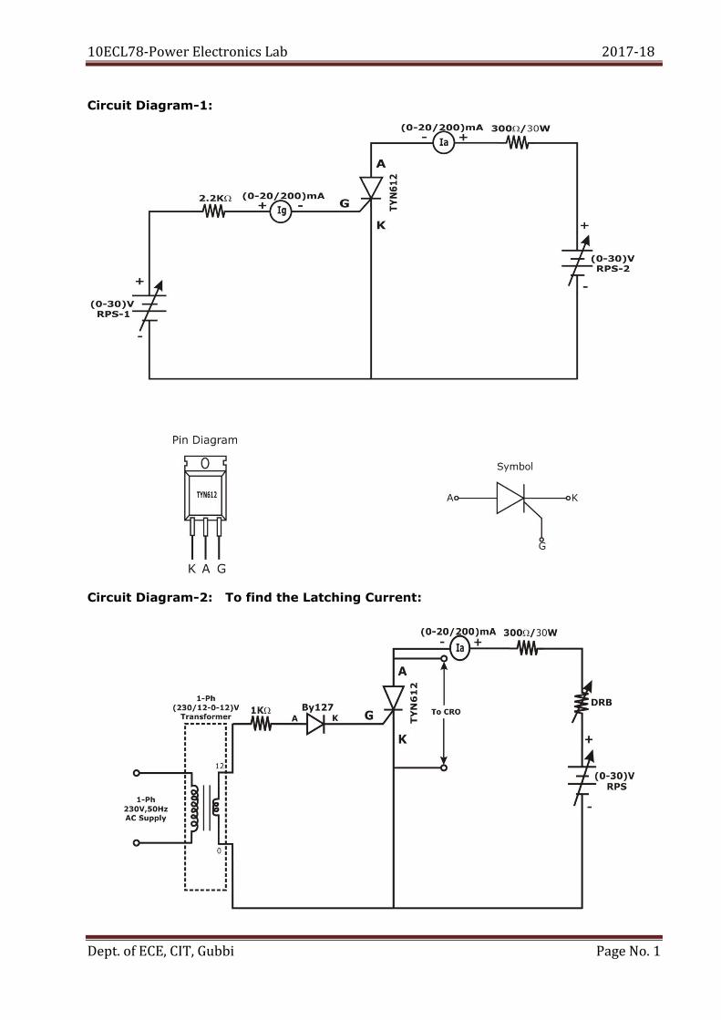
Circuit Diagram-1:
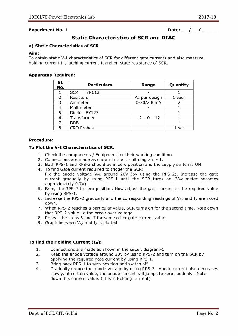
Circuit Diagram-2: To find the Latching Current:
10ECL78-Power Electronics Lab 2017-18
Dept. of ECE, CIT, Gubbi Page No. 2
Experiment No. 1 Date: __ /__ / _____
Static Characteristics of SCR and DIAC
a) Static Characteristics of SCR
Aim:
To obtain static V-I characteristics of SCR for different gate currents and also measure
holding current IH, latching current IL and on state resistance of SCR.
Apparatus Required:
Sl.
No. Particulars Range Quantity
1. SCR TYN612 - 1
2. Resistors As per design 1 each
3. Ammeter 0-20/200mA 2
4. Multimeter - 1
5. Diode BY127 - 1
6. Transformer 12 – 0 – 12 1
7. DRB - 1
8. CRO Probes - 1 set
Procedure:
To Plot the V-I Characteristics of SCR:
1. Check the components / Equipment for their working condition.
2. Connections are made as shown in the circuit diagram - 1.
3. Both RPS-1 and RPS-2 should be in zero position and the supply switch is ON
4. To find Gate current required to trigger the SCR:
Fix the anode voltage VAK around 20V (by using the RPS-2). Increase the gate
current gradually by using RPS-1 until the SCR turns on (VAK meter becomes
approximately 0.7V).
5. Bring the RPS-2 to zero position. Now adjust the gate current to the required value
by using RPS-1.
6. Increase the RPS-2 gradually and the corresponding readings of VAK and IA are noted
down.
7. When RPS-2 reaches a particular value, SCR turns on for the second time. Note down
that RPS-2 value i.e the break over voltage.
8. Repeat the steps 6 and 7 for some other gate current value.
9. Graph between VAK and IA is plotted.
To find the Holding Current (IH):
1. Connections are made as shown in the circuit diagram-1.
2. Keep the anode voltage around 20V by using RPS-2 and turn on the SCR by
applying the required gate current by using RPS-1.
3. Bring back RPS-1 to zero position and switch off.
4. Gradually reduce the anode voltage by using RPS-2. Anode current also decreases
slowly, at certain value, the anode current will jumps to zero suddenly. Note
down this current value. (This is Holding Current).

10ECL78-Power Electronics Lab 2017-18
Dept. of ECE, CIT, Gubbi Page No. 3
Latching Current IL
Holding Current IH
IA in mA
0
IG1 IG2
VBO1
VBR
IA
VAK
IG2> IG1
Ron = VAK / IA
VBO2
Design:
VAK = VAA – IA RA
RA = (VAA – VAK) / IA
Assume VAAmax = 30 V, VAKon = 0.7 V, and IA = 100 mA
Then RA = 293 choose RA = 300
and PRA = ( VAAmax – VAKon )2 / RA = 2.86 W
Therefore RA = 300 / 10 W
Tabular Column:
IG1 = _________ mA, VBO1 = __________ V
VAK in Volts IA in mA
Ideal Graph:
IG2 = _________ mA, VBO2 = _______ V
VAK in Volts IA in mA
VAK in V
10ECL78-Power Electronics Lab 2017-18
Dept. of ECE, CIT, Gubbi Page No. 4
To find the Latching Current (IL):
1. Connections are made as shown in the circuit diagram-2.
2. Keep DRB in maximum resistance position
3. Apply the VAA around 20V by using RPS
4. Observe the square waveform across the anode and cathode of SCR (now SCR is
operating in Gate dependent mode)
5. Now reduce the DRB (from higher range to lower) gradually till the square wave
disappears (now SCR is operating in Gate independent mode)
6. Note down the anode current at which the square wave disappear (This is Latching
Current)
Calculation:
On state resistance Ron = VAK / IA = __________
Result:
The on state resistance of SCR Ron = ________
The holding current IH = ________________ mA
The latching current IL = ________________ mA
At gate current IG1 = _________ mA the break over voltage VBO1 = ________ V
IG2 = _________ mA the break over voltage VBO2 = ________ V

10ECL78-Power Electronics Lab 2017-18
Dept. of ECE, CIT, Gubbi Page No. 5
Circuit Diagram-3:
Structure of DIAC Circuit Symbol of DIAC
Design: -
PDIAC = VDIAC x IDMAX
IDMAX = mA8.17V28
w5.0
V
P
DIAC
DIAC
Ra(min) =
k79.1mA8.17
2860
I
VV
D(max)
DIACaa
P(max) = I a(min)
2
(max)D R = (17.8 mA)2 x 1.79k
= 0.56 W
Choose Ra = 2 k /1W
Ideal Graph:
2kΩ /1W
10ECL78-Power Electronics Lab 2017-18
Dept. of ECE, CIT, Gubbi Page No. 6
b) Static Characteristics of DIAC
Aim:
To Design & study the V-I characteristics of DIAC and determine the Break over
voltage.
Apparatus Required:
Sl.
No. Particulars Range Quantity
1. DIAC-DB3 - 1
2. Power Supplies 0-60V 1
3. Wattage Resistors 2kΩ/1W 1
4. Ammeter 0-20/200mA 1
5. Multimeter - 1
Procedure:
1 Connections are made as shown in the circuit diagram-3.
2 Consider as T1 is positive w.r.t. T2 and by varying the supply voltage gradually
in step-by step, note down the corresponding values of V & I.
3 Note down V & I at the instant of firing of DIAC and after firing (by reducing
the voltmeter ranges and increasing the ammeter ranges) then increase the
supply voltage V. Note down corresponding values of V & I.
4 The point at which DIAC fires, gives the value of break over voltage VBO1.
5 Plot a graph of V V/S I.
6 Now consider T2 is positive w.r.t T1 and repeat steps no. 2, 3 & 4.
Tabular Column:
Forward Characteristics:
V in Volts IF in mA -V in Volts -IF in mA
Result:
Reverse Characteristics:

10ECL78-Power Electronics Lab 2017-18
Dept. of ECE, CIT, Gubbi Page No. 7
Ic
VGE
Ic(mA)
VCE(V)
VGE1
VGE2 Ic VCE
VCE1
VCE2
VGE(V)
Circuit Diagram-4:
Ideal Graph:
Transfer Characteristics: Output Characteristics
Ic(mA)
300 / 30W
VGE2> VGE1
VCE2> VCE1
Constant resistance
region
Constant current region
10ECL78-Power Electronics Lab 2017-18
Dept. of ECE, CIT, Gubbi Page No. 8
Experiment No.2 Date: __ /__ / _____
Static Characteristics of MOSFET and IGBT
a) Static Characteristics of IGBT
Aim:
To conduct an experiment to plot the transfer characteristics and output characteristics of an
IGBT and to find the transconductance and output resistance.
Apparatus Required:
Sl.
No. Particulars Range Quantity
1. IGBT-G4BC20S - 1
2. Ammeter 0-20/200mA 1
3. Multimeter - 1
Procedure:
Transfer Characteristics:
1. Check the components / Equipment for their working condition.
2. Connections are made as shown in the circuit diagram-4.
3. Initially both RPS-1 and RPS-2 are kept at zero output position.
4. By varying the RPS-2, set VCE around 1V.
5. Now increase VGE by varying the RPS-1 gradually and note down the corresponding
collector current.
6. Repeat the steps 4 and 5 for some other VCE value (Say 2V).
7. Draw the graph between VGE and Ic.
Output Characteristics:
1. Check the components / Equipment for their working condition.
2. Connections are made as shown in the circuit diagram-4.
3. Both RPS-1 and RPS-2 should be in zero output position and supply switch is ON
4. By varying RPS-1, set VGE to some value (slightly greater than the Threshold voltage
determined from the transfer characteristics).
5. Now increase the VCE by varying the RPS-2 gradually and note down the
corresponding collector current.
6. Repeat the steps 4 and 5 for some other VGE value.
7. Graph between VCE Vs Ic is plotted.
10ECL78-Power Electronics Lab 2017-18
Dept. of ECE, CIT, Gubbi Page No. 9
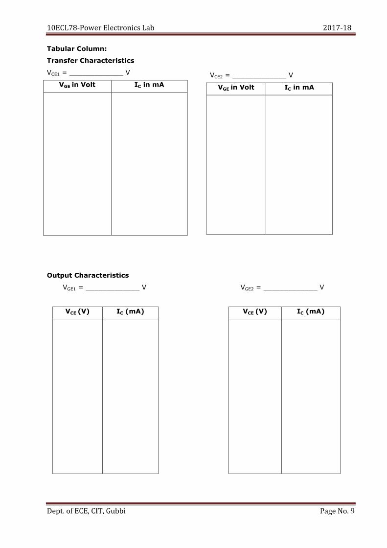
Tabular Column:
Transfer Characteristics
VCE1 = _____________ V
VGE in Volt IC in mA
Output Characteristics
VGE1 = _____________ V VGE2 = _____________ V
VCE (V) IC (mA) VCE (V) IC (mA)
VCE2 = _____________ V
VGE in Volt IC in mA

10ECL78-Power Electronics Lab 2017-18
Dept. of ECE, CIT, Gubbi Page No. 10
Calculations:
Trans conductance gm =Ic / VGE = ____________ mho
Output Resistance Ro =VCE / Ic = ____________
Results:
The transconductance gm = ______________ mho
The output resistance Ro = ______________

10ECL78-Power Electronics Lab 2017-18
Dept. of ECE, CIT, Gubbi Page No. 11
ID
VGS
ID(mA)
VDS(V)
VGS1
VGS2 ID
VDS
VDS1
VDS2
Circuit diagram-5:
Ideal Graph:
Transfer Characteristics: Drain Characteristics
ID(mA)
VT VGS(V)
300Ω/30W
VGS2> VGS1
VDS2> VDS1
Constant resistance
region
Constant current region
10ECL78-Power Electronics Lab 2017-18
Dept. of ECE, CIT, Gubbi Page No. 12
b) Static Characteristics of MOSFET
Aim :
To conduct an experiment for plotting the transfer characteristics and drain characteristics of
an MOSFET and to find the transconductance and drain resistance.
Apparatus Required:
Sl.
No. Particulars Range Quantity
1. MOSFET (IRF 540) - 1
2. Milliammeter 0-20/200mA 1
3. Multimeter - 1
Procedure:
Transfer Characteristics:
1. Check the components / Equipment for their working condition.
2. Connections are made as shown in the circuit diagram-5.
3. Initially both RPS-1 and RPS-2 are kept at zero output position.
4. By varying the RPS-2, set VDS around 3V.
5. Now increase VGS by varying the RPS-1 gradually and note down the corresponding
drain current.
6. Repeat the steps 4 and 5 for some other VDS value.
7. Draw the graph between VGS and ID.
Output Characteristics:
1. Check the components / Equipment for their working condition.
2. Connections are made as shown in the circuit diagram-5.
3. Both RPS-1 and RPS-2 should be in zero output position and supply switch is ON.
4. By varying RPS-1, set VGS to some value (slightly greater than the Threshold voltage
determined from the transfer characteristics).
5. Now increase the VDS by varying the RPS-2 gradually and note down the
corresponding drain current.
6. Repeat the steps 4 and 5 for some other VGS value.
7. Graph between VDSVs ID is plotted.

10ECL78-Power Electronics Lab 2017-18
Dept. of ECE, CIT, Gubbi Page No. 13
Tabular Column:
Transfer Characteristics
VDS1 = _____________ V VDS2 = _____________ V
VGS (V) ID (mA)
Output/Drain Characteristics:
VGS1 = _____________ V VGS2 = _____________ V
VDS (V) ID (mA) VDS (V) ID (mA)
VDS2 = _____________ V
VGS (V) ID in mA
10ECL78-Power Electronics Lab 2017-18
Dept. of ECE, CIT, Gubbi Page No. 14
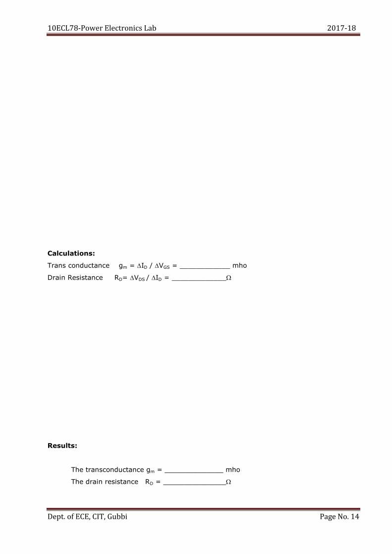
Calculations:
Trans conductance gm = ID / VGS = ____________ mho
Drain Resistance RD= VDS / ID = _____________
Results:
The transconductance gm = ______________ mho
The drain resistance RD = _______________
10ECL78-Power Electronics Lab 2017-18
Dept. of ECE, CIT, Gubbi Page No. 15
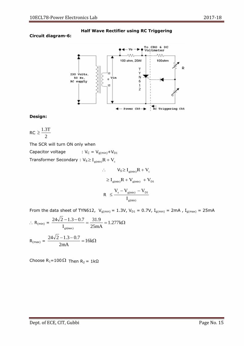
Half Wave Rectifier using RC Triggering
Circuit diagram-6:
Design:
RC 2
1.3T
The SCR will turn ON only when
Capacitor voltage : VC = Vg(min)+VD1
Transformer Secondary : VS cg(min) V RI
VS cg(min) V RI
D1 g(min)g(min) VV RI
R
g(min)
D1 g(min)s
I
VVV
From the data sheet of TYN612, Vg(min) = 1.3V, VD1 = 0.7V, Ig(min) = 2mA , Ig(max) = 25mA
R(min) =
k277.1mA25
9.31
I
7.03.1224
gt(max)
R(max) =
k16mA2
7.03.1224
Choose R1=100 Then R2 = 1kΩ
T Y N 6 1 2
R

10ECL78-Power Electronics Lab 2017-18
Dept. of ECE, CIT, Gubbi Page No. 16
Experiment No.3 Date: __ /__ / _____
Controlled HWR and FWR using RC triggering circuit
Aim:
To study the performance & waveforms of HWR & FWR by using RC triggering Circuit.
Apparatus Required:
Sl.
No. Particulars Range Quantity
1. SCR – TYN612 - 1
2. Transformer 230/12-0-12 V 1
3. CRO Probe - 1 set
4. Diode- BY127 1
5. Resistor - 2
6. DRB,DCB 1
Procedure:
1. Connections are made as shown in circuit diagram-6,7.
2. Keep the value of DRB at 1K and DCB at 0.1uf. Switch ON the supply.
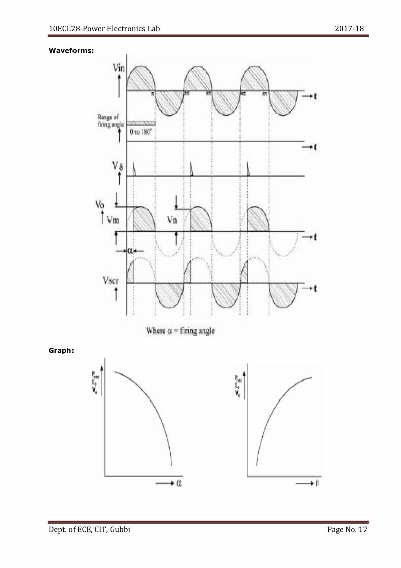
3. Now vary the firing angle by increase the value of resistance in DRB in steps, observe the
waveforms and note down the corresponding values of Vn and Vmfrom CRO and Vodcfrom
the DC voltmeter. The readings are tabulated in the tabular column.
4. If the firing angle ranges from 0 to 90º, then the firing angle α is calculated by using
formula α = sin-1(Vn/Vm) in degrees.
5. The conduction angle β is calculated using the formula, β = 180-α.
6. The current and power is calculated by Iodc = Vodc/R ampere and Podc = V2odc/R Watts
respectively.
7. A graph of Vo v/s α, Vo v/s β, Io v/s α, Io v/s β, Podcv/s α and Podcv/s β are to be plotted.
8. Compare the practical output voltage with the theoretical output voltage,
(
) ( ) V. Where Vm = √2*Vrms.
10ECL78-Power Electronics Lab 2017-18
Dept. of ECE, CIT, Gubbi Page No. 17
Waveforms:
Graph:
10ECL78-Power Electronics Lab 2017-18
Dept. of ECE, CIT, Gubbi Page No. 18
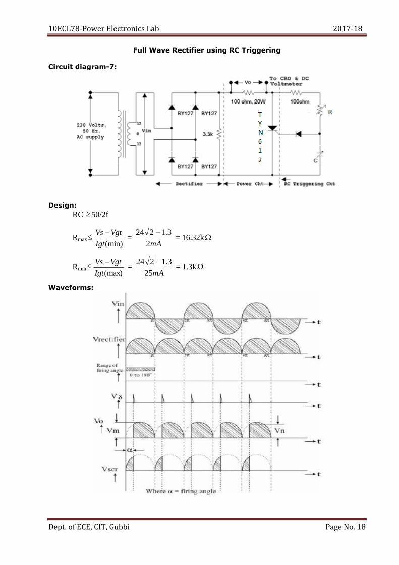
Full Wave Rectifier using RC Triggering
Circuit diagram-7:
Design:
RC 50/2f
Rmax(min)Igt
VgtVs =
mA2
3.1224 = 16.32k
Rmin(max)Igt
VgtVs =
mA25
3.1224 = 1.3k
Waveforms:

10ECL78-Power Electronics Lab 2017-18
Dept. of ECE, CIT, Gubbi Page No. 19
Tabular Columns:
Half Wave Rectifier: Vm=____________V
Sl.
No. Vn
α<90º α>90º
Vodc Voth ( ) (
)
Full Wave Rectifier: Vm=____________V
Sl.
No. Vn
α<90º α>90º
Vodc Voth ( ) (
)

10ECL78-Power Electronics Lab 2017-18
Dept. of ECE, CIT, Gubbi Page No. 20
Simulation:
HWR:
FWR:
Result:
10ECL78-Power Electronics Lab 2017-18
Dept. of ECE, CIT, Gubbi Page No. 21
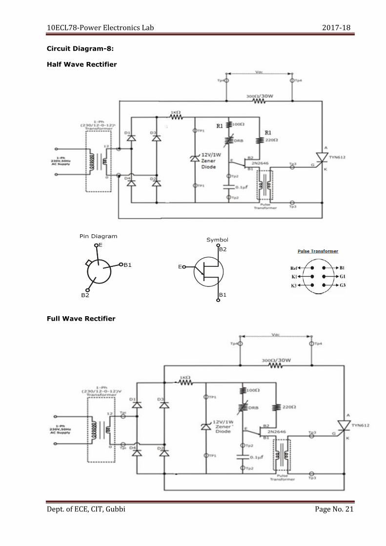
Circuit Diagram-8:
Half Wave Rectifier
Full Wave Rectifier
10ECL78-Power Electronics Lab 2017-18
Dept. of ECE, CIT, Gubbi Page No. 22
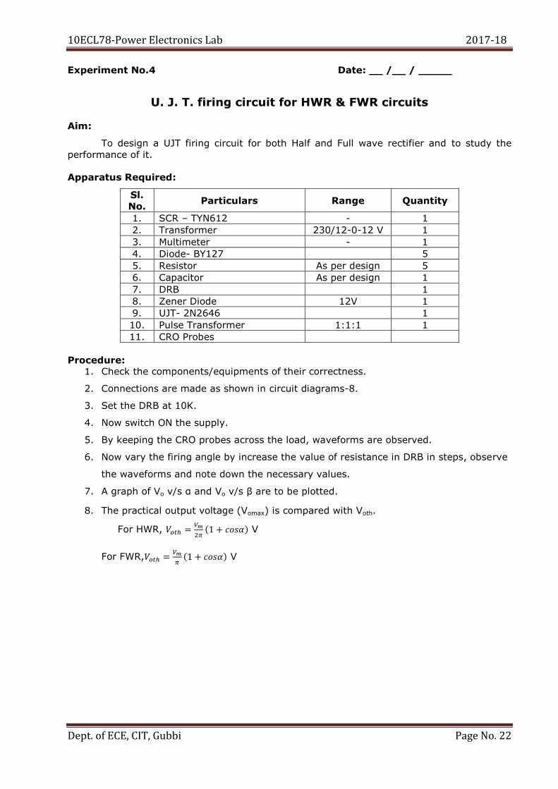
Experiment No.4 Date: __ /__ / _____
U. J. T. firing circuit for HWR & FWR circuits Aim:
To design a UJT firing circuit for both Half and Full wave rectifier and to study the
performance of it.
Apparatus Required:
Sl.
No. Particulars Range Quantity
1. SCR – TYN612 - 1
2. Transformer 230/12-0-12 V 1
3. Multimeter - 1
4. Diode- BY127 5
5. Resistor As per design 5
6. Capacitor As per design 1
7. DRB 1
8. Zener Diode 12V 1
9. UJT- 2N2646 1
10. Pulse Transformer 1:1:1 1
11. CRO Probes
Procedure: 1. Check the components/equipments of their correctness.
2. Connections are made as shown in circuit diagrams-8.
3. Set the DRB at 10K.
4. Now switch ON the supply.
5. By keeping the CRO probes across the load, waveforms are observed.
6. Now vary the firing angle by increase the value of resistance in DRB in steps, observe
the waveforms and note down the necessary values.
7. A graph of Vo v/s α and Vo v/s β are to be plotted.
8. The practical output voltage (Vomax) is compared with Voth.
For HWR,
( ) V
For FWR,
( ) V
10ECL78-Power Electronics Lab 2017-18
Dept. of ECE, CIT, Gubbi Page No. 23
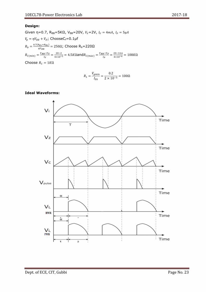
Design:
Given η=0.7, RBB=5KΩ, VBB=20V, =2V, ,
; ChooseCf=0.1µf
( )
; Choose Rb=220Ω
( )
and ( )
Choose
Ideal Waveforms:
10ECL78-Power Electronics Lab 2017-18
Dept. of ECE, CIT, Gubbi Page No. 24
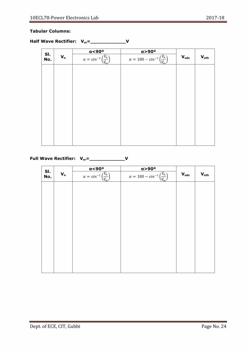
Tabular Columns:
Half Wave Rectifier: Vm=____________V
Sl.
No. Vn
α<90º α>90º
Vodc Voth ( ) (
)
Full Wave Rectifier: Vm=____________V
Sl.
No. Vn
α<90º α>90º
Vodc Voth ( ) (
)

10ECL78-Power Electronics Lab 2017-18
Dept. of ECE, CIT, Gubbi Page No. 25
Ideal Graph: VDC (V)
0 180 in deg
Calculations:

10ECL78-Power Electronics Lab 2017-18
Dept. of ECE, CIT, Gubbi Page No. 26
Simulation Circuit:
Note: Similarly Construct for FWR
Result:

10ECL78-Power Electronics Lab 2017-18
Dept. of ECE, CIT, Gubbi Page No. 27
Circuit Diagram-9:
10ECL78-Power Electronics Lab 2017-18
Dept. of ECE, CIT, Gubbi Page No. 28
Experiment No. 5 Date: __ /__ / _____
Digital firing circuit for
Single phase fully controlled Rectifier
Aim:
To draw the output waveforms of fully controlled rectifier using digital triggering circuit
Apparatus Required:
Sl.
No. Particulars Range Quantity
1. 1-Phase fully controlled
rectifier unit - 1
2. Digital triggering circuit
unit - 1
3. CRO with probes 1
Procedure:
1. Digital firing circuit kit T1, T2, T3 and T4 terminals are connected with the
corresponding SCR terminals in the rectifier unit.
2. Ensure the thumb wheel switch (F.A/D.cy) in the DFC kit should show „000‟ and the
toggle switch in 180o position.
3. Now switch ON rectifier unit then DFC kit.
4. Observe the output waveforms across the Load.
5. Vary the firing angle by varying the thumb wheel switch (F.A/D.cy) in the DFC kit in
steps and observe the waveform.
Circuit given is for fully controlled bridge rectifier. Students can try for Half Wave and Semi-
controlled Converter.
Note:For the detailed operation of DFC refer Appendix.

10ECL78-Power Electronics Lab 2017-18
Dept. of ECE, CIT, Gubbi Page No. 29
Waveforms:

10ECL78-Power Electronics Lab 2017-18
Dept. of ECE, CIT, Gubbi Page No. 30
Tabular Column:
Sl. No. α in degrees VDC in Volts
Ideal Graph:
VDC(V)
(deg)
Result:
Resistive Load
Inductive Load

10ECL78-Power Electronics Lab 2017-18
Dept. of ECE, CIT, Gubbi Page No. 31
Circuit Diagram-10:

10ECL78-Power Electronics Lab 2017-18
Dept. of ECE, CIT, Gubbi Page No. 32
Experiment No.6 Date: __ /__ / _____
Single phase Fully Controlled Bridge Converter
with R and R-L loads Aim:
To conduct an experiment on single phase fully controlled rectifier with R, R-L loads and vary
the DC output voltage.
Apparatus Required:
Sl.
No. Particulars Range Quantity
1. 1- FullyControlledBridge
converter Module - 1
2. Fully Controlled Bridge Firing
Module - 1
3. Resistor 300 / 30 W 1
4. Diode BY127 - 1
5. Transformer 12 – 0 – 12 1
6. CRO with Probes - 1
7. Multimeter - 1
8. Resistive-Inductive Load - 1
Procedure:
1. Firing module triggering pulses are connected with the corresponding SCR terminals
in the rectifier unit.
2. Ensure the firing angle variation POT is in zero position.
3. Now switch ON rectifier unit and then firing module.
4. By keeping the CRO probes across the Load (R, R-L) the waveforms are observed.
5. Now vary the firing angle by turning the POT in steps, observe the waveforms and
note down the necessary values.
6. The graph between Vs VDC is plotted (for both R & R-L load).

10ECL78-Power Electronics Lab 2017-18
Dept. of ECE, CIT, Gubbi Page No. 33
Waveforms:
Tabular Column:
Vm = _____________ V : T = _________ ms
Sl.
No.
t
(mSec)
(deg)
(deg)
VDC(V)
(R - Load )
VDC(V)
(R-L Load )
Note: = T
t* 180 : = 180 -
Ideal Graph:
VDC(V)
(deg)
Calculations:
Resistive Load
Inductive Load

10ECL78-Power Electronics Lab 2017-18
Dept. of ECE, CIT, Gubbi Page No. 34
Result:
10ECL78-Power Electronics Lab 2017-18
Dept. of ECE, CIT, Gubbi Page No. 35
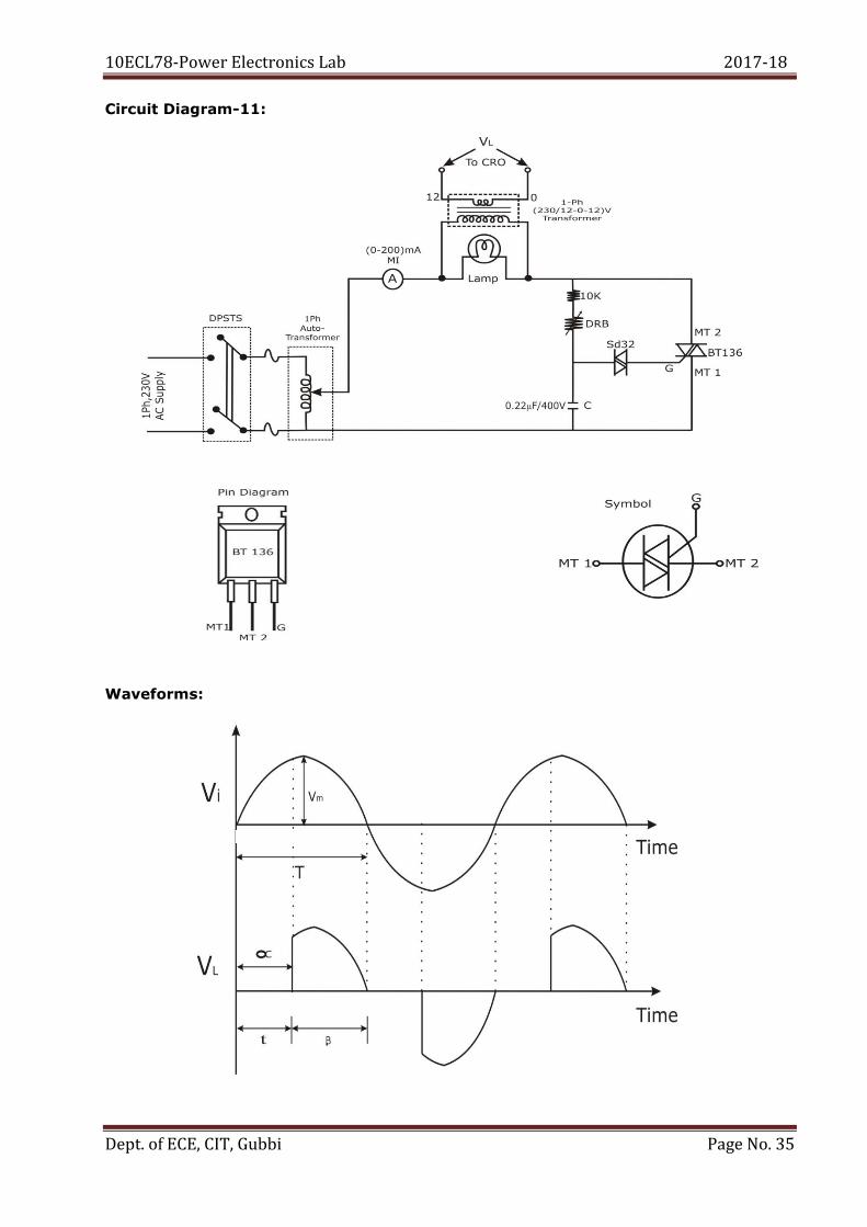
Circuit Diagram-11:
Waveforms:
10ECL78-Power Electronics Lab 2017-18
Dept. of ECE, CIT, Gubbi Page No. 36
Experiment No. 7 Date: __ /__ / _____
AC Voltage Control by using TRIAC-DIAC Combination
Aim: To conduct an experiment to control the AC voltage using TRIAC-DIAC combination.
Apparatus Required:
Sl.
No. Particulars Range Quantity
1. TRIAC BT136 - 1
2. DIAC SD32 - 1
3. Resistor & Capacitor As per design 1 each
4. Dimmerstat (1-ph Auto-Trans.) - 1
5. Transformer 12 – 0 – 12 1
6. DRB - 1
7. CRO with Probes - 1
8. Incandescent Lamp 60W 1
9. Multimeter - 1
10. AC Milliammeter (0-200)mA (MI) 1
Procedure:
1. Check the components/equipments for their correctness.
2. Connection are made as shown in circuit diagram-11.
3. Set the DRB in minimum resistance position.
4. Keep the 1-Phase Auto-transformer in zero output position and the supply switch is
ON.
5. Set the Auto-transformer output voltage around 150V (use Multimeter to measure).
6. Increase the DRB value in steps and observe Irms and Vrms (measure across
transformer secondary) values and tabulate it.
7. Bring back the Auto-transformer output to Zero position and the supply switch is OFF.
8. The graph between Vs Vrms and Vs Irms are plotted.
Note: Since 150V AC input is applied do not touch any components when supply is
Switched ON.
10ECL78-Power Electronics Lab 2017-18
Dept. of ECE, CIT, Gubbi Page No. 37
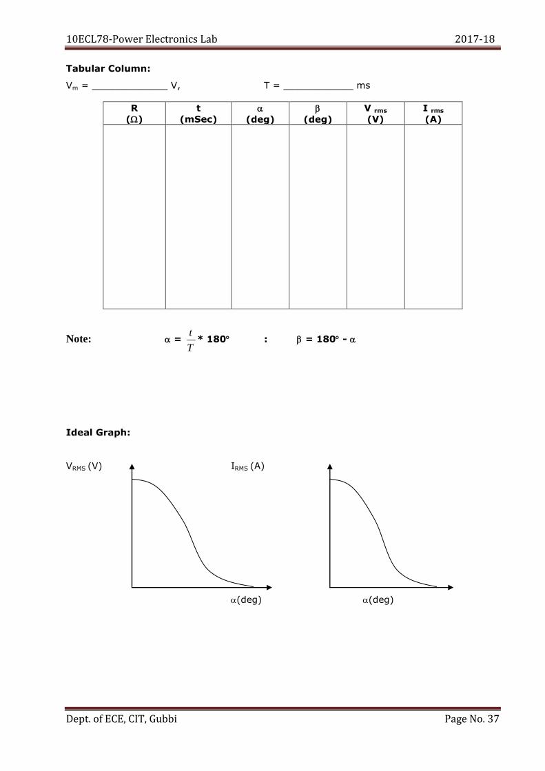
Tabular Column:
Vm = _____________ V, T = ____________ ms
R
()
t
(mSec)
(deg)
(deg)
V rms
(V)
I rms
(A)
Note: = T
t* 180 : = 180 -
Ideal Graph:
VRMS (V) IRMS (A)
(deg) (deg)

10ECL78-Power Electronics Lab 2017-18
Dept. of ECE, CIT, Gubbi Page No. 38
Result:

10ECL78-Power Electronics Lab 2017-18
Dept. of ECE, CIT, Gubbi Page No. 39
Impulse Commutated Chopper:
Circuit Diagram-12
Wave forms:
10ECL78-Power Electronics Lab 2017-18
Dept. of ECE, CIT, Gubbi Page No. 40
Experiment No.8 Date: __ /__ / _____
Voltage (Impulse) Commutated Chopper both constant frequency and
variable frequency operations
a) Constant frequency operation:
Aim:
To study the performance of voltage commutated chopper for constant frequency
operations.
Apparatus Required:
Sl.
No. Particulars Range Quantity
1. SCR-TYN612 - 2
2. Resistors 30Ω/30W 1
3. DIB - 1
4. Diode-BY127 - 1
7. DCB - 1
8. Power supply 1
9. Firing module 1
Procedure:
1. Connections are made as shown in the circuit diagram-12.
2. Input DC voltage is set to convenient value (4v to 11v).
3. By varying duty cycle knob of triggering circuit module step by step gradually note
down corresponding Ton and T from the CRO and VO from DC voltmeter and tabulate.
4. Duty cycle „D‟ is calculated by using
D= TON/T
5. A graph of VO v/s D is plotted.
6. Observe load and device voltage waveforms.
10ECL78-Power Electronics Lab 2017-18
Dept. of ECE, CIT, Gubbi Page No. 41
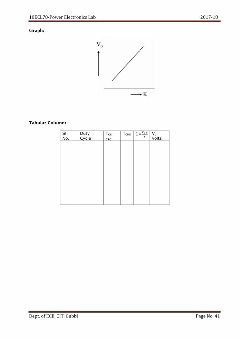
Graph:
Tabular Column:
Sl.
No.
Duty
Cycle
TON
CRO
TCRO D=
Vo
volts
10ECL78-Power Electronics Lab 2017-18
Dept. of ECE, CIT, Gubbi Page No. 42
b) Variable frequency operation:
Aim:
To study the performance of voltage commutated chopper for variable frequency
operations.
Apparatus:
Sl.
No. Particulars Range Quantity
1. SCR-TYN612 - 2
2. Resistors 30Ω/30W 1
3. DIB - 1
4. Diode-BY127 - 1
5. DCB - 1
6. Power supply 1
7. Firing module 1
Procedure:
1. Connections are made as shown in the circuit diagram-12 for constant frequency
operation.
2. Input DC voltage is set to convenient value (10V to 25V).
3. Vary the output voltage by changing the duty ratio,
D=
by keeping Ton or Toff constant and note down Vo from DC voltmeter and tabulate.
4. Observe load and device voltage waveforms also tabulate the values accordingly.
5. A graph of VO v/s f is plotted.
Tabular Column:
Sl. No. Duty Cycle TON CRO TCRO D=
Vo volts
Result:

10ECL78-Power Electronics Lab 2017-18
Dept. of ECE, CIT, Gubbi Page No. 43
Circuit Diagram-13:
10ECL78-Power Electronics Lab 2017-18
Dept. of ECE, CIT, Gubbi Page No. 44
Experiment No.9 Date: __ /__ / _____
Speed Control of a Separately Excited DC Motor Aim:
To study speed control of DC motor and record armature voltage and speed for
different values of α.
Apparatus Required:
Sl.
No. Particulars Range Quantity
1. DC Motor speed control unit - 1
2. Sep. excited DC Motor 1
2. Tachometer Contact Type 1
3. Connecting probes - -
Procedure:
1. Check the components/equipments of their correctness
2. Keep the voltage selector switch in OFF position and supply switch is ON.
3. The LCD display shows –
POWER MOSFET/IGBT CHOPPER
0FF DCY – 0: FRQ - 50
Digital volt meter and ammeter shows 000
4. Measure the Field voltage using digital voltmeter. It should be 220V ± 10%
approximately and the neon lamp glows.
5. Now keep the voltage select switch at position 1 and measure the voltage at VDC
terminals. It should be 24 volts. The output voltage should be 48 volts when VOLT-
SELECT switch at position – 2, 110 volts when the VOLT-SELECT switch at position –
3, 220 volts when the VOLT-SELECT switch position at 4 approximately.
6. Make sure that the DC supply is correct. Now observe the driver output using CRO
by varying duty cycle and frequency.
7. Make sure that the driver output is proper before connecting to the gate/emitter or
gate/source of IGBT or MOSFET.
8. Now all the outputs are proper. Make the connections as given in the circuit diagram
8.1.
9. Vary the duty cycle in steps and keep the frequency as constant and observe the
speed of the motor and note down the values of V, I and RPM.
10. Now change the frequency in steps and keep the duty cycle as constant and tabulate
the necessary values.
11. Draw the graph between duty cycle Vs speed and Frequency Vs speed.
NOTE: Connect field supply to the field terminals of the Motor before connecting
to the armature supply. And the field supply should be removed only
after switching OFF the armature supply.
10ECL78-Power Electronics Lab 2017-18
Dept. of ECE, CIT, Gubbi Page No. 45
Tabular Columns:
Vin=_________V : Frequency=_______Hz
Vin=_________V : Duty cycle =_______%
Duty cycle
(%)
Vout
(V)
Io
(A)
Speed
(rpm)
Frequency
(Hz)
Vout
(V)
Io
(A)
Speed
(rpm)

10ECL78-Power Electronics Lab 2017-18
Dept. of ECE, CIT, Gubbi Page No. 46
Chopper Simulation Circuit:
Result:
10ECL78-Power Electronics Lab 2017-18
Dept. of ECE, CIT, Gubbi Page No. 47
Universal Motor (DC):
Circuit Diagram-14:
Universal Motor (AC)
Graph:
Circuit Diagram-15:
Tabular column
DC motorAC Motor
Vm=________V T=_______ms
VDC Speed
(rpm)
t
(mSec)
(deg)
(deg)
Vrms
(V)
Speed
(RPM)
10ECL78-Power Electronics Lab 2017-18
Dept. of ECE, CIT, Gubbi Page No. 48
Experiment No. 10 Date: __ /__ / _____
Speed Control of Universal Motor
Aim:
To study speed control of Universal motor and plot speed v/s α.
Apparatus Required:
Sl.
No. Particulars Range Quantity
1. Universal Motor 1
2. Tachometer Contact Type 1
3. Connecting probes - -
4. Diode-IN4001
Procedure:
DC Motor:
a. Connections are made as shown in circuit diagram-14.
b. Vary the Firing angle by varying resistor pot, note down the value of Vn, Vm,
VDC and speed.
c. Calculate firing angle.
d. Plot the graph of speed verses firing angle.
Note : For AC operation resistor value is varied using DRB and for DC operation use resistor
pot.
AC Motor:
a. Connections are made as shown in circuit diagram-15.
b. Above procedure is repeated for AC Motor.
Note: = T
t* 180 : = 180 -
Result:
10ECL78-Power Electronics Lab 2017-18
Dept. of ECE, CIT, Gubbi Page No. 49
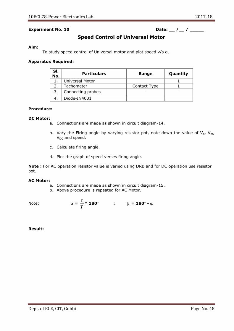
Circuit Diagram-16:

10ECL78-Power Electronics Lab 2017-18
Dept. of ECE, CIT, Gubbi Page No. 50
Experiment No. 11 Date: __ /__ / _____
Single phase full bridge Inverter/Parallel Inverter
a) Bridge Inverter
Aim: To conduct an experiment on 1-phase full bridge PWM Inverter (IGBT based)
Apparatus Required:
Sl.
No. Particulars Range Quantity
1. 1-phase full bridge Inverter
Module - 1
2. Rheostat (0-100) /5A 1
3. Connecting probes - -
Procedure:
1. Now make the connections as given in the circuit diagram-16.
2. Connect DC supply from (0-30) V regulated power supply unit.
3. Connect resistive load 0–100 ohms 5 Amps Rheostat at load terminals (keep the
sliding switch in middle position).
4. Connect driver output signals to the Gate and Emitter of corresponding IGBTs.
5. Switch ON the DC supply.
6. SwitchON the mains supply. The LCD display shows 1-ph PWM inverter with
modulation type and M- (modulation index) 00 and F-100 Hz and in OFF position.
Now M-00 Blinks. Press INC key to set the M.I. from 00- 100%.
7. Set the Modulation Index value in steps (keep the frequency as constant) and
press the Run/STOP button then measure the output voltage and tabulate it.
8. Set the frequency value in steps (keep the M.I value as constant) and press the
Run/STOP button then measure the output voltage and tabulate it.
.
NOTE: The SET key works only when it is in OFF position. This is to avoid change of
modulation type when the power circuit is ON.
.

10ECL78-Power Electronics Lab 2017-18
Dept. of ECE, CIT, Gubbi Page No. 51
Tabular column:
Modulation Type: ____________ Frequency: ____________
Modulation Type: ____________ Frequency: ____________
Modulation Type: ____________ Modulation Index: ____________
Modulation Index
(%)
Output voltage
(V)
Modulation Index
(%)
Output voltage
(V)
Frequency
(Hz)
Output voltage
(V)

10ECL78-Power Electronics Lab 2017-18
Dept. of ECE, CIT, Gubbi Page No. 52
Modulation Type: ____________ Modulation Index: ____________
Simulation Circuit:
Result:
Frequency
(Hz)
Output voltage
(V)

10ECL78-Power Electronics Lab 2017-18
Dept. of ECE, CIT, Gubbi Page No. 53
Circuit Diagram-17:
Firing Module:
Design:
√
Circuit designed for operating frequency of f=1kHz ,Assume C=0.1µF
Calculate L:
√ ( )
L= 3.94H
+ 15V G1
GND K1, K2
- 15 V G2

10ECL78-Power Electronics Lab 2017-18
Dept. of ECE, CIT, Gubbi Page No. 54
b) Parallel Inverter
Aim: To convert DC to AC using Parallel Inverter
Apparatus Required:
Sl.
No. Particulars Range Quantity
1. Thyristor‟s TYN612 2
2. DCB - 1
3. DIB - 1
4. Transformer 12V-0-12V
9V-0-9V 1
Procedure:
1. Make the connections as given in the circuit diagram.
2. Connect DC supply from (0-5) V regulated power supply unit.
3. Check the triggering pulses from firing module.
4. Switch ON the DC supply.
5. Adjust DCB and DIB to convert DC to AC.
6. Note down the frequency of AC Signal.
Result:
10ECL78-Power Electronics Lab 2017-18
Dept. of ECE, CIT, Gubbi Page No. 55
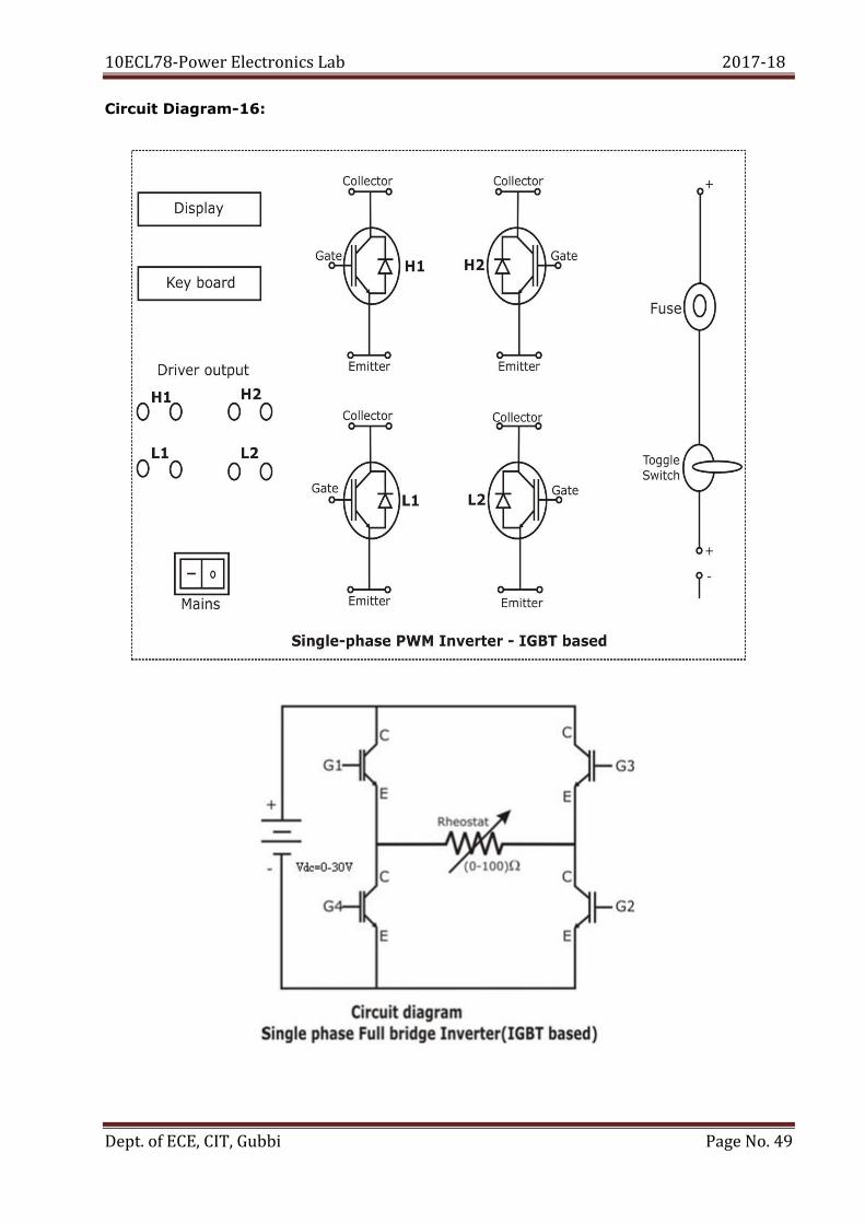
Commutation Circuit
Circuit Diagram-18:
Design:
Given η=0.7, RBB=5KΩ, VBB=20V, =2V, ,
; Assume Cf=0.1µf
( )
; Choose Rb=220Ω
( )
and ( )
Choose
Waveform:
Pulse Transformer

10ECL78-Power Electronics Lab 2017-18
Dept. of ECE, CIT, Gubbi Page No. 56
Experiment No. 12 Date: __ /__ / _____
LC Commutation Circuit (Class B Commutation Circuit)
Aim:
To conduct an experiment to study the LC commutation circuit.
Apparatus Required:
Sl.
No. Particulars Range Quantity
1. SCR TYN 612 - 1
2. UJT 2N2646 - 1
3. Diode BY127 - 1
4. Pulse Transformer - 1
5. CRO Probes - 1 set
6. Multimeter - 1
7. DCB - 2
8. DRB and DIB - 1 each
9. Resistor 30 / 30W
100, 220 1 each
Procedure:
1. Check the components / Equipment for their working condition.
2. Connections are made as shown in the circuit diagram-18.
3. Set the value of Cf around 0.1 f and observe the triggering pulses in the pulse
transformer.
4. Set the value of L around 1 to 5 mH and C around 1 to 10 Farads apply the input
signal (Vi/p).
5. Observe the output waveform across the load.
6. By varying the value of Cf or L or C vary TON, and TOFF.
7. Note down TON and TOFF and plot a graph of Duty cycle Vs VDC
10ECL78-Power Electronics Lab 2017-18
Dept. of ECE, CIT, Gubbi Page No. 57
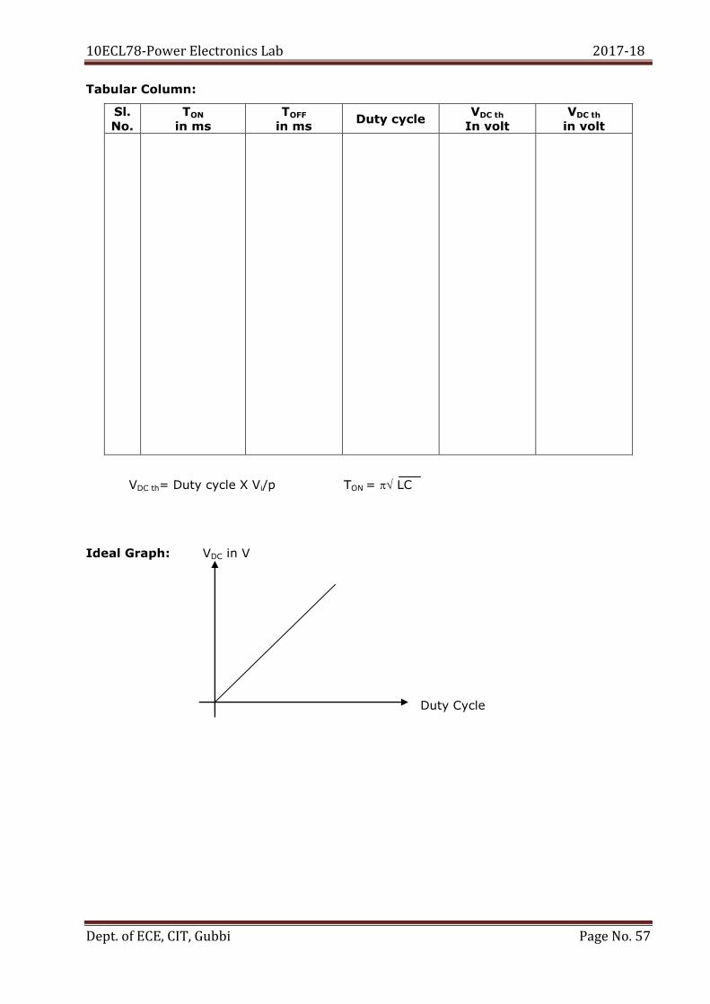
Tabular Column:
Sl.
No.
TON
in ms
TOFF
in ms Duty cycle
VDC th
In volt
VDC th
in volt
VDC th= Duty cycle X Vi/p TON = LC
Ideal Graph: VDC in V
Duty Cycle
10ECL78-Power Electronics Lab 2017-18
Dept. of ECE, CIT, Gubbi Page No. 58
Calculations:
Result:

10ECL78-Power Electronics Lab 2017-18
Dept. of ECE, CIT, Gubbi Page No. 59
Circuit diagram:
10ECL78-Power Electronics Lab 2017-18
Dept. of ECE, CIT, Gubbi Page No. 60
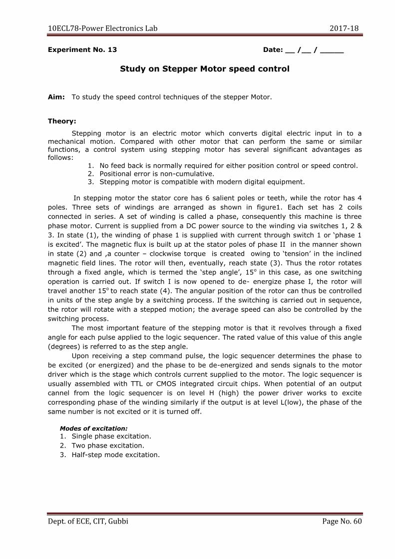
Experiment No. 13 Date: __ /__ / _____
Study on Stepper Motor speed control
Aim: To study the speed control techniques of the stepper Motor.
Theory:
Stepping motor is an electric motor which converts digital electric input in to a
mechanical motion. Compared with other motor that can perform the same or similar
functions, a control system using stepping motor has several significant advantages as
follows:
1. No feed back is normally required for either position control or speed control.
2. Positional error is non-cumulative.
3. Stepping motor is compatible with modern digital equipment.
In stepping motor the stator core has 6 salient poles or teeth, while the rotor has 4
poles. Three sets of windings are arranged as shown in figure1. Each set has 2 coils
connected in series. A set of winding is called a phase, consequently this machine is three
phase motor. Current is supplied from a DC power source to the winding via switches 1, 2 &
3. In state (1), the winding of phase 1 is supplied with current through switch 1 or „phase 1
is excited‟. The magnetic flux is built up at the stator poles of phase II in the manner shown
in state (2) and ,a counter – clockwise torque is created owing to „tension‟ in the inclined
magnetic field lines. The rotor will then, eventually, reach state (3). Thus the rotor rotates
through a fixed angle, which is termed the „step angle‟, 15o in this case, as one switching
operation is carried out. If switch I is now opened to de- energize phase I, the rotor will
travel another 15o to reach state (4). The angular position of the rotor can thus be controlled
in units of the step angle by a switching process. If the switching is carried out in sequence,
the rotor will rotate with a stepped motion; the average speed can also be controlled by the
switching process.
The most important feature of the stepping motor is that it revolves through a fixed
angle for each pulse applied to the logic sequencer. The rated value of this value of this angle
(degrees) is referred to as the step angle.
Upon receiving a step command pulse, the logic sequencer determines the phase to
be excited (or energized) and the phase to be de-energized and sends signals to the motor
driver which is the stage which controls current supplied to the motor. The logic sequencer is
usually assembled with TTL or CMOS integrated circuit chips. When potential of an output
cannel from the logic sequencer is on level H (high) the power driver works to excite
corresponding phase of the winding similarly if the output is at level L(low), the phase of the
same number is not excited or it is turned off.
Modes of excitation:
1. Single phase excitation.
2. Two phase excitation.
3. Half-step mode excitation.

10ECL78-Power Electronics Lab 2017-18
Dept. of ECE, CIT, Gubbi Page No. 61

10ECL78-Power Electronics Lab 2017-18
Dept. of ECE, CIT, Gubbi Page No. 62
Single phase excitation: Table1 shows the sequences of a single phase excitation mode for
3 & 4 phase motor. The shaded parts in the table represent the excited state, & the white
blanks show the phases to which current is not supplied & so are not excited. The operation
by single phase excitation is also known as 1 phase on drive.
Two phase excitation: The operation of a motor in which 2 phases are always excited is
called 2 phases on operation. The sequence for 3 & 4 phases motor are shown in table 2.
Half step mode excitation: The excitation scheme that is a combination of single phase &
2 phase excitation is so called half step operation. The excitation sequence for three phase
motor is given in table 3.
10ECL78-Power Electronics Lab 2017-18
Dept. of ECE, CIT, Gubbi Page No. 63
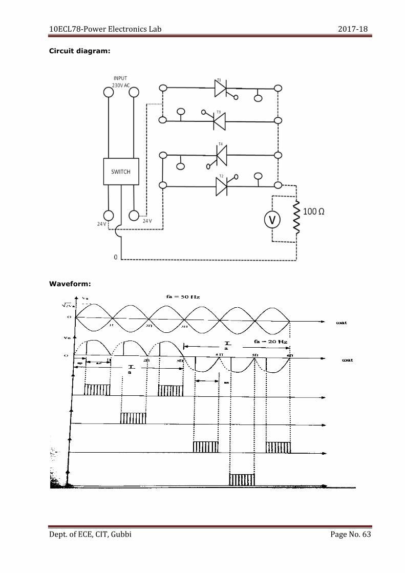
Circuit diagram:
Waveform:
10ECL78-Power Electronics Lab 2017-18
Dept. of ECE, CIT, Gubbi Page No. 64
Experiment No. 14 Date: __ /__ / _____
Study on Cyclo Converters
Aim: To study the working of a single phase centre tap transformer type cyclo-converter.
ApparatusRequired:
Sl.
No. Particulars Range Quantity
1. Cyclo converter kit - 01
2. Resistor 100Ω/30watt 01
3. Digital Multimeter - 01
4. Patch chords - As required
Procedure:
1. Switch ON the mains supply to the firing circuit.
2. Observe the trigger outputs by changing frequency division and by
varying the firing angle.
3. Make sure that the firing pulses are proper before connecting to the
power circuit.
4. Next make the power circuit connections as given in the circuit.
5. Connect the firing pulses from the firing circuit to the respective SCR‟s
in the power circuit.
6. Connect R-load (50 ohms/ 25Watts) or 24V lamp at the output.
7. Connect 24-0-24 V input AC supply from the centre tap transformer.
8. Switch ON the AC supply to the power circuit.
9. Keep the firing angle at 1800 and frequency division at 2. Switch ON
the trigger outputs.
10. Vary the firing angle and note down the AC voltage across load using
multimeter and tabulate the readings.
11. Draw the voltage wave forms for different firing angle. Repeat the same
for different frequency division.
12. The circuit works as single phase AC voltage controller when the
frequency division is at 1. It works as cyclo converter from 2-10
division.
10ECL78-Power Electronics Lab 2017-18
Dept. of ECE, CIT, Gubbi Page No. 65
Tabular column:
SL. No. N (per cycle) Vo

10ECL78-Power Electronics Lab 2017-18
Dept. of ECE, CIT, Gubbi Page No. 66
Result:
10ECL78-Power Electronics Lab 2017-18
Dept. of ECE, CIT, Gubbi Page No. 67
VIVA QUESTIONS-1
Static Characteristics of SCR, TRIAC
1. Explain the construction details of a thyristor.
2. What are the applications of SCR.
3. Define Latching current and Holding current.
4. Define forward break over voltage.
5. Explain the working of SCR with the help of two transistor analogy.
6. Explain different thyristor turn on methods.
7. Explain dv/dt and di/dt protection circuits of a thyristor.
8. Explain different types of thyristors.
9. Explain the importance of series and parallel operation of thyristors.
10. Define the turn off time of SCR.
11. Explain the V-I characteristics of SCR.
12. Explain the V-I characteristics of TRIAC.
13. Explain the different modes of operation of an TRIAC.
14. What are the applications of SCR.
15. What are the applications of TRIAC.
16. Explain how do we find latching current.
Static Characteristics of MOSFET, IGBT
1. Explain the constructional details of MOSFET.
2. Explain the construction details of IGBT.
3. Explain different types of MOSFETs.
4. Compare enhancement and depletion MOSFETs.
5. Define Pinch off voltage, threshold voltage of MOSFETs.
6. Explain the characteristics of MOSFET.
7. Explain the characteristics of IGBT.
8. Explain the advantages and disadvantages of MOSFET.
9. Explain the advantages and disadvantages of IGBT.
10. Explain the control characteristics of MOSFET and IGBT.
11. Compare IGBT with BJT.
12. Compare MOSFET with BJT.
13. What are the applications of MOSFET and IGBT.
Controlled HWR, FWR using RC triggering, UJT triggering Circuit
1. What is a firing circuit. Why is it needed.
2. What are the requirements of a firing circuit.

10ECL78-Power Electronics Lab 2017-18
Dept. of ECE, CIT, Gubbi Page No. 68
3. Explain R triggering circuit.
4. What are the advantages of pulse triggering circuits.
5. Compare R triggering and RC triggering circuits.
6. Explain the working of RC triggering circuit.
7. Explain the construction of UJT.
8. Explain the V-I characteristics of UJT.
9. Explain the working of UJT triggering circuit.
10. Explain the principle of digital firing circuits.
11. What is the roll of pulse transformer.
AC Voltage Controller using TRIAC-DIAC Combination
1. How TRIAC can be used in AC voltage controller.
2. Explain the working of the circuit given for AC voltage controller.
3. Explain the characteristics of DIAC.
4. What are the applications of AC voltage controllers.
5. What type of triggering is suitable for ac voltage controller with inductive load.
Single phase half and full controlled converter
1. What is a controlled converter.
2. What are the performance parameters of a converter.
3. Compare half controlled converter and full controlled converter.
4. What is the effect of inductive load on converters.
5. Explain the roll of free wheeling diode.
6. explain the working of a controlled converter.
7. What is a dual converter.
8. Compare single phase and three phase converters.
9. What are the applications of controlled converters.
LC and Auxiliary commutation circuits.
1. What is a commutation circuit.
2. Why do we need commutation circuits.
3. Compare natural or line commutation and forced commutation.
4. What are different types of commutation circuits. With the help of neat circuit diagram
explain the working of each circuit.
5. Explain the working of LC commutation circuit.
6. Explain the working of Auxiliary commutation circuit.
7. What is a chopper.
8. What are the types of chopper.

10ECL78-Power Electronics Lab 2017-18
Dept. of ECE, CIT, Gubbi Page No. 69
9. Explain the principle of step down and step up choppers.
10. Explain the working of voltage commutated chopper.
11. What are the application of choppers.
12. What is pulse width modulation control of a chopper.
13. What is the frequency modulation control of a chopper.
14. What are the applications of choppers.
15. Explain the classifications of choppers.
Speed control of Induction motor and DC motor
1. Explain the working of the circuit used for speed control of Induction motor.
2. Explain the working of the circuit used for DC motor.
3. What type of triggering pulses are used in speed control of motor circuits.

10ECL78-Power Electronics Lab 2017-18
Dept. of ECE, CIT, Gubbi Page No. 70
Viva Questions-2
1. What is power Electronics?
2. Mention the different methods of varying the power?
3. What are the advantages of silicon over germanium?
4. What is power device?
5. Mention the different types of power devices?
6. What is an SCR?
7. What are the features of SCR?
8. What are the applications of SCR?
9. What is a Diac?
10. What are the features of Diac?
11. What are the applications of Diac?
12. What is a Triac?
13. What are the features of Triac?
14. What are the applications of Triac?
15. What is power MOSFET?
16. What is power IGBT?
17. What are the applications of MOSFET & IGBT?
18. Compare SCR, DIAC & TRIAC?
19. Compare MOSFET, BJT & IGBT?
20. What is turn on time?
21. What is turn off time?
22. What is static Characteristics?
23. What is dynamic Characteristics?
24. What is the difference between the Static & Dynamic Characteristics?
25. Explain the Turn on Characteristics & Turn off Characteristics of SCR?
26. Explain the gate characteristics of SCR?
27. What is a current controlled device?
28. What is a Voltage controlled device?
29. Explain O/p & Transfer characteristics of MOSFET & IGBT?
30. Explain the intension of using power device in power control circuit?
31. What is a power control?
32. Why SCR is called as Unidirectional Controlled device?
33. Why Diac is called as Bidirectional controlled device?
34. Why Triac is called as Bidirectional controlled device?
35. What is rectifier?
36. What is an Inverter?
37. What is step down chopper? What is its o/p voltage equation?

10ECL78-Power Electronics Lab 2017-18
Dept. of ECE, CIT, Gubbi Page No. 71
38. What is step up chopper? What is its o/p voltage equation?
39. What is buck boost regulator? What is its o/p Voltage equation?
40. What is cuck regulator? What is its o/p Voltage equation?
41. Explain the working operation of single phase controlled Half wave rectifier with a) R
Load (b) RL Load (c) RL load with free wheeling diode
42. What is an intention of using free wheeling across inductive load in rectifier circuit?
43. What is pulse width?
44. Why turn off time of the circuit should be greater than turn off time of the device?
45. Explain the working operation of single phase full wave controlled rectifier with
a) R Load (b) RL Load (c) RL load with free wheeling diode
46. Explain the working operation of single phase half wave controlled rectifier with
a) R Load (b) RL Load (c) RL load with free wheeling diode
47. Explain the working operation of single phase full controlled bridge rectifier with a) R
Load (b) RL Load (c) RL load with free wheeling diode
48. Define average output voltage, RMS Voltage, peak or maximum voltage?
49. Derive an expression of average output voltage, RMS output voltage of any wave
form concerned to rectifier, ac voltage controller, chopper?
50. What are cyclo converters?
51. What is cyclo inverter?
52. Why forced commutation circuit is employed in case of cyclo inverter?
53. What are the advantages of three phase circuit over single phase circuit?
54. What is firing angle or delay angle?
55. What is conduction period?
56. What is meaning of triggering?
57. What are the different types of triggering methods (can be used to trigger SCR)?
58. What are the different types of triggering methods, temperature triggering, light
triggering and gate triggering?
59. Why gate triggering is preferred than other types?
60. Mention the different types of gate triggering circuit?
61. Explain the working operation of RC triggering circuit?
62. Why firing angle in case of R triggering circuit if limited to 90 degrees?
63. Explain the working operation of RC Triggering circuit?
64. Explain how firing angle will be extended to more than 900 by using Rc triggering
Circuit?
65. What is Unijunction Transistor (UJT)?
66. Write equivalent circuit of UJT?
67. Show that V peak=Vp =nVBB + V diode where n = intrinsic stand off ration, VBB=
applied or base voltage?
10ECL78-Power Electronics Lab 2017-18
Dept. of ECE, CIT, Gubbi Page No. 72
68. Why UJT triggering circuit is superior than R & RC triggering circuit?
69. What is UJT Relaxation oscillation?
70. What is line synchronized UJT triggering circuit?
71. Explain the working operation of UJT relaxation oscillator?
72. Explain the working operation of line synchronized UJT triggering circuit with wave
forms at different points?
73. Design of UJT triggering circuit?
74. When UJT will conduct?
75. How UJT exhibits negative resistance property?
76. Why SCR, DIAC, TRIAC are called negative resistance devices?
77. Derive an expression of frequency of UJT triggering pulse?
78. What is the function of pulse transformer?
79. What are the different types of voltage ratings, current ratings and power ratings?
Explain each them?
80. Why do we require protection circuits for power devices?
81. What is di/dt rating? How do you protect SCR against high di/dt rating? explain
82. What is dv/dt rating? How do you protect SCR against high dv/dt rating? explain
83. What is over current? How do you protect SCR against over current? explain
84. What is over voltage? How do you protect SCR against over voltage? Explain
85. How device will be protected against heavy power dissipation?
86. Why triac has 4 modes of operations?
87. Why 1st& 2nd mode of operations are operating in 1st Quadrant and 3rd& 4th mode of
operations are operating 3rd quadrant?
88. Why mod (1) is mot sensitive among all modes?
89. What is Commutation?
90. What is commutation circuit?
91. What is forced commutation circuit and natural commutation circuit?
92. Mention the different types of forced commutation circuits?
93. Explain the working operation of each forced commutation circuit with wave forms &
derivation of designed equations ( Class A, Class B, Class C, Class D, Class E and
Class F commutation circuit)
94. What is latching current? What is its significance?
95. What is holding current? What is its significance?
96. What is dv/dt rating? What is its significance?
97. What is dual converter?
98. Why full wave bridge controller bridge rectifier with RL Load (not with free wheeling
diode) is preferred in dual converter than half wave bridge controlled rectifier with RL
load (not free wheeling diode)?

10ECL78-Power Electronics Lab 2017-18
Dept. of ECE, CIT, Gubbi Page No. 73
99. Why dual converter is called as four quadrant operator?
100. What is semi converter?
101. What is full converter?
102. Why gate is preferred at base of NPN transistor & not at the base of PNP
transistor in SCR?
103. Derive an expression of anode current (SCR Current)?
104. Explain the working operation of SCR with two transistor analogy?
105. Explain the working operation of each practical power Electronics experiments with
circuit diagram, wave forms & designed equation?
106. Why output voltage is more at lesser value of firing angle?
107. What are the differences between uncontrolled output & controlled output?
108. How do you design zener voltage regulator?
109. How do you select (design) the value of gate resistor and load resistor
concerned to SCR experiments?
110. Why do you check SCR, Triac, Diac, Diode, Zener Diode, wires by using ohm
meter?
111. How do you check an ammeter, voltmeter & power supply?
112. Why load resistor has higher wattage?
113. What is series Inverter? Mention the advantages, disadvantages and application
of series inverter? Explain its working operation?
114. What is parallel inverter? Explain its working operation?
115. What is continuous mode & discontinuous mode of operations concerned to
rectifier with a) RL Load b) RL load with free wheeling diode?
116. Input voltage = device voltage + output voltage. Prove above words?
117. What are the blocking & reverse blocking?
118. What is blocking state or region?
119. What is forward blocking and reverse blocking?
120. What is reverse recovery time?
121. What is gate pulse?
122. Why gate pulses are preferred than continuous gate voltage ?
123. S.T Turn on time =td + tr + ts
124. S.T Turn off time =trr +tgr
125. How do you design gate pulse width?
126. What is snubber circuit? How do you design snubber?
127. What is heat sink its purpose is what?
128. What is circuit breaker and fuse? Why these are used in power circuit?
129. What is ac voltage controller? Mention the different types? What are its
applications?

10ECL78-Power Electronics Lab 2017-18
Dept. of ECE, CIT, Gubbi Page No. 74
130. Explain the working operation of a) on and off AC Voltage controller b)
Unidirectional or Half wave controller C) Bidirectional or full wave AC Voltage
controller with R load and RL Load with wave forms with equations?
131. Why continuous gate pulses are applied to full wave ac voltage controller with RL
Load circuit?
132. Explain the working operation of static on load tap changer?
133. Why negative gate voltage should not be applied to gate of SCR?
134. Write symbols, static characteristics of all power devices concerned to syllabus?
135. Name different current controlled power devices?
136. Name different Voltage controlled power devices?
137. What is I2 t rating?

10ECL78-Power Electronics Lab 2017-18
Dept. of ECE, CIT, Gubbi Page No. 75
Question Bank
1. Conduct a suitable experiment to obtain the V-I characteristics of the SCR and
determine holding current, latching current and on state resistance.
2. Conduct a suitable experiment to determine the V-I characteristics of
unidirectional four layer switch for two different gate currents. Determine
breakdown voltage for two cases.
3. Conduct a suitable experiment to obtain the V-I characteristics of the DIAC.
Experimentally determine the breakdown voltage in quadrant-I and Quadrant-
III.
4. Conduct a experiment to obtain transfer characteristics and output
characteristics of an IGBT. Determine the value of trans-conductance and
output resistance.
5. Design and simulate an experiment toobtain transfer characteristics and drain
characteristics of an MOSFET. Determine the value of trans-conductance and drain resistance.
6. Design and simulate an experiment using SCR in an half wave rectifier circuit to vary the DC voltage fed to load using R-C triggering circuit. Plot a graph of
output DC voltage v/s firing angle ( ).
7. Design and simulate an experiment using SCR in an full wave rectifier circuit
to vary the DC voltage fed to load using R-C triggering circuit. Plot a graph of
output DC voltage v/s firing angle ( ).
8. Conduct an experiment to control the illumination of an incandescent lamp
using TRIAC-DIAC combination. Plot a graph of Vrms v/s firing angle ( ) and
Irms v/s firing angle.
9. Conduct a suitable experiment on half / full controlled converterbridge with R
and RL load. Plot a graph of output DC voltage v/s firing angle ( ).
10ECL78-Power Electronics Lab 2017-18
Dept. of ECE, CIT, Gubbi Page No. 76
10.Conduct an experiment to turn off SCR by using LC commutation circuit. Plot
graph of duty cycle v/s output DC voltage.
11.Conduct an experiment to turn off SCR by using Auxiliary commutation circuit.
Plot graph of duty cycle v/s output DC voltage.
12.Conduct an experiment to obtain AC output voltage using bridge inverter
circuit.
13.Conduct a suitable experiment to control the speed of a stepper motor.
14.Conduct a suitable experiment to control the speed of a DC motor. Plot a
graph of speed v/s firing angle ( ).
15.Conduct a suitable experiment to control the speed of a universal motor. Plot
a graph of speed v/s firing angle ( ).
16.Conduct an experiment to generate the firing signals for thyristors/ triacs
using digital circuits/ microprocessor.
17.Design and simulate an experiment toobtain synchronized triggering pulses using UJT to turn on an SCR in a full wave rectifier/half wave rectifier with
resistive load. Plot a graph of output DC voltage v/s firing angle ( ).
18.Conduct an experiment to convert fixed DC voltage to variable DC voltage by
using voltage commutated chopper. Plot a graph of duty cycle v/s output DC
voltage.
* * * * * *
10ECL78-Power Electronics Lab 2017-18
Dept. of ECE, CIT, Gubbi Page No. 77
REFERENCES
1. SCR Manual, 5th Edition, N.Y., General Electric Company, 1972.
2. B.K.Bose, „Power Electronics and AC Drives‟, Prentice-Hall, Englewood
Cliffs, New Jersey 07632, 1986.
3. P.C.Sen, ”Thyristorised DC Drive”, New York: Wiley Interscience, 1981
4. B.K.Bose, „Evaluation of Modern Power Semiconductor Devices and
Future Trends of Converters‟, IEEE Trans. Industry Applications, vol.
28, No. 2, pp. 403-413, March/April, 1992.
5. NED MOHAN, „Power Electronics‟, John Wiley and Sons, 1989.
6. M.H.Rashid, „Power Electronics‟, Prentice-Hall of India, New Delhi,
1993.
7. G.K.Dubey and C.R.Kasarabada, “Power Electronics and Drives”, IETE
Book Series, Vol. 1, TM HILL P.C.Ltd., New Delhi – 1993.
8. B.K.Bose,”Energy, environment and advances in Power Electronics”,
IEEE Trans. On P.E. Vol 15, No.4, July 2000.
9. O.P. Arora, „Power Electronics Laboratory, Theory Practice and
Organization‟,2010, NAROSA publishing house private limited.