(12) unitedstatespatent us8,373,609b1
TRANSCRIPT

(12) United States Patent
Dorsey et al.
US008373609B1
US 8,373,609 B1
Feb. 12, 2013
(10) Patent No.:
(45) Date of Patent:
(54) PERTURBED SQUARE RING SLOT ANTENNA
WITH RECONFIGURABLE POLARIZATION
(75) Inventors: W Mark Dorsey, Elkridge, MD (US);
Amir I Zaghloul, Bethesda, MD (US);
Mark G Parent, Port Tobacco, MD (US)
(73) Assignees: The United States ofAmerica, as
represented by the Secretary of the
Navy, Washington, DC (US); Virginia
Tech Intellectual Properties, Inc.,
Blacksburg, VA (US)
( * ) Notice: Subject to any disclaimer, the term of this
patent is extended or adjusted under 35
U.S.C. 154(b) by 669 days.
(21) Appl.No.: 12/481,025
(22) Filed: Jun. 9, 2009
Related US. Application Data
(60) Provisional application No. 61/060,289, filed on Jun.
10, 2008.
(51) Int. Cl.
H01Q 13/10 (2006.01)
(52) US. Cl. ....................................................... 343/769
(58) Field of Classification Search 343/700 MS,
343/767, 768, 769, 770
See application file for complete search history.
(56) References Cited
U.S. PATENT DOCUMENTS
4,379,296 A 4/1983 Farrar et a1.
4,728,960 A 3/1988 L0
5,596,336 A 1/1997 Liu
7,187,337 B2 * 3/2007 Aikawa et a1. ................ 343/767
7,535,326 B2 5/2009 Nakatani et a1.
FOREIGN PATENT DOCUMENTS
WO W001207l8 Al * 3/2001
OTHER PUBLICATIONS
S.H. Hsu and K. Chang, “A Novel Reconfigurable Microstrip
Antenna with Switchable Circular Polarization”, IEEE Antennas and
Wireless Propagation Let., v01. 6, pp. 160-162 (2007).
YJ. Sung, T.U. Jang, and Y.S. Kim, “A Reconfigurable Microstrip
Antenna for Switchable Polarization”, IEEE Microwave & Wireless
Components Let., v01. 14, pp. 534-536 (Nov. 2004).
ST. Fang, “A Novel Polarization Diversity Antenna for WLAN
Applications”, Antennas and Prop. Society International Sympo-
sium, v01. 1, pp. 282-285 (Jul. 2000).
F. Yang and Y. Rahmat-Samii, “A Reconfigurable Patch Antenna
Using Switchable Slots for Circular Polarization Diversity”, IEEE
Microwave and Wireless Components Letters, v01. 12, N0. 3, pp.
96-98 (Mar. 2002).
M. Niroojazi and MN. Azarmanesh, “Practical Design of Single
Feed Truncated Corner Microstrip Antenna”, Proceedings of the
Second Annual Conference on Communication Networks and Ser-
vices Research, v01. 00, pp. 25-29.
P.C. Sharma and KC. Gupta, “Optimized Design of Single Feed
Circularly Polarized Microstrip Patch Antennas”, Antennas and
Propagation Society International Symposium, v01. 20, pp. 156-159
(May 1982).
(Continued)
Primary Examiner 7 Robert Karacsony
(74) Attorney, Agent, or Firm 7 Amy L. Ressing; L. George
Legg
(57) ABSTRACT
A reconfigurable polarization antenna includes a microwave
dielectric substrate having a ground plane that has a centrally
located slot with five conducting patches, four ofwhich form
an evenly spaced apart perimeter group with a gap between
each and the fifth, centrally positioned conducting patch. A
conducting pad is positioned in each gap and is connected via
a switch to the ground plane. A microstrip feed line including
a short stub is positioned on the opposite side ofthe substrate
and electromagnetically coupled to the slot. The polarization
of the antenna is reconfigured by a selection of an on or off
state of each of said switches.
13 Claims, 11 Drawing Sheets

US 8,373,609 B1
Page 2
OTHER PUBLICATIONS
J.S. Row, “The Design of a Squarer-Ring Slot Antenna for Circular
Polarization”, IEEE Transactions on Antennas and Propagation, vol.
53, No. 6, pp. 1967-1972 (Jun. 2005).
RM. Sorbello and AI. Zaghloul, “Wideband, High-Efficiency, Cir-
cularly Polarized Slot Elements”, Antennas and Propagation Society
International Symposium, vol. 3, pp. 1473-1476 (Jun. 1989).
Fries, Grani, and Vahldieck presented an annular slot antenna with
switchable polarization in “A Reconfigurable Slot Antenna With
Switchable Polarization”, IEEE Microwave and Wireless Compo-
nents Letters, vol. 13, No. 11, pp. 490-492 (Nov. 2003).
* cited by examiner

US. Patent Feb. 12, 2013 Sheet 1 of 11 US 8,373,609 B1
PIN DIODE ’V E» T “ j
\ 1
r. 1 4
rout 'n 2 3 4+
\ V1x SHOF'ITING
CAPACITOR
FIG. 1A FIG. 18
PRIOR ART PRIOR ART
LI
TN

US. Patent Feb. 12, 2013 Sheet 2 of 11 US 8,373,609 B1
q QUARTER-
WAVE 509
TRANSFORMER UNE
DIODE 1 DIODE2
DIODE 4 DIODE 3
A
FIG. 2
PRIOR ART
US. Patent Feb. 12, 2013 Sheet 3 of 11 US 8,373,609 B1
FIG. 3
PRIOR ART

U.S. Patent Feb. 12, 2013 Sheet 4 of 11 US 8,373,609 B1
22'
'
29°95
9/?”/20
FIG. 4B

U.S. Patent Feb.12,2013 Sheet 5 of 11 US 8,373,609 B1
RHCP
LHCP
LP
FIG. 5

US. Patent Feb. 12, 2013 Sheet 6 of 11 US 8,373,609 B1
5 I | I I
4 — SIMULATED _____________
n: —e— MEASURED 1 1 . 1
E 3—-------------1--------------- 1 -------------- 1--------------- 'r ---------- .-------------- >> I I
2 ---------- I ----- ------: ----------------------------------------- I ---------
1 I I I I I
9 9.5 10 10.5 11 11.5 12
FREQUENCWGHz)
5 I | I I
4 —SIMULATED ______________________________________________
n: —e— MEASURED 1 1
E 3 ------------- 1--------------- 1 -------------- 1--------------- r -------------- 1 ---------------> I I I
2'""""""1'""""""" I """ v"""5“"3I I fii I
19 9.5 10 10.5 11 11.5 12
FREQUENCWGHZ)
5 I | I I
4 — SIMULATED _______________
u: —e— MEASURED , . i iE 3—------------- 1--------------- 1 -------------- 1--------------- 1 -------------- 1---------------> I I
2 ' --------------- I ------------- >
19 9.5 10 10.5 11 11.5 12
FREQUENCWGHZ)
FIG. 6C

US. Patent Feb. 12, 2013 Sheet 7 of 11 US 8,373,609 B1
E - 5 l l l
451‘--------------i----------------§""""“""""+'--LHCP'
20 g g g --- RHCP
925 915 1025 1075 1125
FREQUENCY(GH3
FIG. 7

US. Patent Feb. 12, 2013 Sheet 8 of 11
40.00 : .
9 0.00- i §
24000- 5 5<1: l l(D I I
2000- -
3000 "'CX'PO': : a a a a a a a
' ' 400 450 4'20 00 0'0 0'0 0 3'0 5'0 0'0 420 450 430
THETA(DEG.)
40.00
r: 0.00 ————————————————————————————————————————————————————————
£40.00-
5 ' : : : : .
-20.00-- :~. i—Co—Pol -
30 00 : : : : : i "I'CX'IPOI
' ' 430 4'50 4'20 00 00 0'0 0 3'0 0'0 9'0 420 450 430
THETA(DEG.)
40.00 . . .
9 0-00' : :
3 i i i i —Co-Pol
E '10'00"""I11':""" "'CX-Pol0 ma : : : ’ ~ :
20.00 ""-'"i"3‘?"'i';:""'::"§:\'"'i'lr'"""""""i"';;:'_'j"';'
'30'09400 4'50 4'20 00 0'0 0'0 '6 3'0 0'0 0'0 420 450 180
THETA(DEG.)
FIG. 80
US 8,373,609 B1

US. Patent Feb. 12, 2013 Sheet 9 of 11 US 8,373,609 B1
GND +v1 GND

US. Patent Feb. 12, 2013 Sheet 10 of 11 US 8,373,609 B1
FIG. 1OB
29< S-I-I-I
29‘ ::: :::
GND +v2 25 +V1GND
E INDUCTOR CAPACITOR
<>D|ODE . PLATED THROUGH HOLE
FIG. 10A
\___________/
FIG. 1OB

US 8,373,609 B1Sheet11,0f11Feb.12,2013U.S. Patent
SEE FIG. IIB
E2\.EEEIEEEEHE
EEEIEIEIEI
EHEIEEIEE!
EEIIEIEIEI
EHIfl/llflflflfl
HIE/HIEIIEIEE
E’E'il\i/fliiifl
"’uununnnuu
EEEIEIEEEE
EEEIEEEEHE
FIG. 11A
FIG. IIB

US 8,373,609 B1
1
PERTURBED SQUARE RING SLOT ANTENNA
WITH RECONFIGURABLE POLARIZATION
CROSS-REFERENCE TO RELATED
APPLICATIONS
This Application claims the benefit of US. Provisional
Application 61/060,289 filed on Jun. 10, 2008.
BACKGROUND OF THE INVENTION
The invention is directed to an antenna with reconfigurable
polarization, and more particularly, to an antenna having a
perturbed square ring slot configuration for operating in mul-
tiple polarizations.
Circular polarized (CP) antennas are popular choices in
mobile wireless communications applications owing to their
ability to allow flexible orientation between the transmitter
and receiver antennas and to reduce multipath effects that can
lead to signal fading, e.g. as described in S. H. Hsu and K.
Chang, “A Novel Reconfigurable Microstrip Antenna with
Switchable Circular Polarization”, IEEE Antennas and Wire-
less Propagation Let., Vol. 6, 2007, pp. 160-162;Y. J. Sung, T.
U. Jang, and Y. S. Kim, “A Reconfigurable Microstrip
Antenna for Switchable Polarization”, IEEE Microwave &
Wireless Components Let., Vol. 14, November 2004, pp.
534-536 (hereinafter “Sung”); and S. T. Fang, “A Novel
Polarization Diversity Antenna for WLAN Applications”,
Antennas and Prop. Society International Symposium, Vol. 1,
16-21 Jul. 2000, pp. 282-285. The ability to efficiently oper-
ate with both senses of CP (LHCP and RHCP) allows the
system to reuse frequencies and double the system capacity,
e.g. as described in F. Yang andY. Rahmat-Samii, “A Recon-
figurable Patch Antenna Using Switchable Slots for Circular
Polarization Diversity”, IEEE Microwave andWireless Com-
ponents Letters, Vol. 12, No. 3, March 2002, pp. 96-98 (here-
inafter “Yang”). Moreover, if the antenna can be switched
between two senses ofCP as well as linearpolarization, it will
allow the user to roam to virtually any existing network, as
described in Sung.
A printed circuit realization is ideal for wireless applica-
tions due to low profile, simple fabrication, low cost, and
compatibility with integrated circuits. A common technique
for achieving circular polarization is to feed the antenna in
two locations with a 90 degree phase shift between the
antenna ports. This technique has the drawbacks ofrequiring
two feed lines as well as a hybrid network of some kind to
provide the necessary phase shift. Single feed circular polar-
ization has been realized in microstrip antennas through the
introduction of a perturbation in opposing comers of the
antenna, e.g. as described in M. Niroojazi and M. N.
Azarmanesh, “Practical Design of Single Feed Truncated
Comer Microstrip Antenna”, Proceedings of the Second
Annual Conference on Communication Networks and Ser-
vices Research, Volume 00, pp. 25-29; P. C. Sharma and
Kuldip C. Gupta, “Analysis and Optimized Design of Single
Feed Circularly Polarized Microstrip Antennas”, IEEE
Transactions on Antennas and Propagation, Vol. AP-31, No.
6, November 1983, pp. 949-955; and P. C. Sharma and K. C.
Gupta, “Optimized Design of Single Feed Circularly Polar-
ized Microstrip Patch Antennas”, Antennas and Propagation
Society International Symposium, Volume 20, May 1982, pp.
156-159. These perturbations introduce a second near-degen-
erate mode. Ifthe antenna is fed correctly, these modes can be
generated with the same amplitude and a 90 degree phase
difference resulting in CP. In these designs, the polarization is
10
15
20
25
30
40
45
50
55
60
65
2
either RHCP orLHCP depending on the relationship between
the feeding microstrip line and the truncated comers.
While traditional microstrip antennas provide a limited CP
bandwidth, printed slot antennas can be more attractive ele-
ments in some cases because they provide an improved oper-
ating bandwidth without increasing the overall size of the
element, e.g. as described in J. S. Row, “The Design of A
Squarer-Ring Slot Antenna for Circular Polarization”, IEEE
Transactions on Antennas and Propagation, Vol. 53, No. 6,
June 2005, pp. 1967-1972. These elements can then be per-
turbed to provide a wideband CP element by applying the
principle ofcomplementary structures to the previously men-
tionedperturbed class ofmicrostrip structures, as described in
R. M. Sorbello and A. I. Zaghloul, “Wideband, High-Elfi-
ciency, Circularly Polarized Slot Elements”, Antennas and
Propagation Society International Symposium, Vol. 3, 26-30
Jun. 1989, pp. 1473-1476.
Antennas with reconfigurable polarization have been a
popular topic in the literature due to their applications in
wireless communications devices. Fries, Grani, and Vahl-
dieck presented an annular slot antenna with switchable
polarization in “A Reconfigurable Slot Antenna With Swit-
chable Polarization”, IEEE Microwave and Wireless Compo-
nents Letters”, Vol. 13, No. 11, November 2003, pp. 490-492
(hereinafter “Fries”). An illustration taken from Fries is
shown in FIG. 1. The authors present two configurations for
this antenna. One antenna can switch between LHCP and
RHCP. The other antenna configuration allows switching
between either LHCP or RHCP and LP, but not all three
states. Thus, each antenna can operate in a maximum oftwo
polarization states.
Sung presents an antenna capable of switching between
LHCP, RHCP, and LP by biasing PIN diode switches to select
the desired truncations on a microstrip patch antenna. This
design, shown in FIG. 2, operates with a bandwidth of less
than 2%. Yang describes a microstrip antenna with polariza-
tion diversity, but their design is limited in switching between
LHCP and RHCP, with no operation possible in LP.
There have been patents issued for antennas with switch-
able polarization. C. C. Liu, “Low Profile TEM Mode Slot
Array Antenna”, US. Pat. No. 5,596,336, issued 21 Jan.
1997, describes a slot array capable of switching polariza-
tions. However, this design requires a polarizing screen to
achieve CP, introducing an extra layer ofcomplexity.Y. T. Lo,
“Multifunctional Microstrip Antennas”, US. Pat. No. 4,728,
960, issued 1 Mar. 1988, describes multifunction microstrip
antenna utilizing truncated corners, but these antennas do not
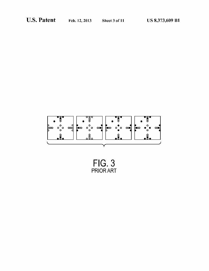
have the ability to switch polarizations. FIG. 3 illustrates the
antenna described in F. G. Farrar and D. H. Schaubert,
“Selectable-mode microstrip antenna and selectable-mode
microstrip antenna arrays”, US. Pat. No. 4,379,296, issued 5
Apr. 1983, where the PIN diodes function as shorting posts at
the desired locations and do not effectively change the shape
of the radiator.
It would therefore be desirable to provide a reconfigurable
antenna without such disadvantages.
BRIEF SUMMARY OF THE INVENTION
According to the invention, a reconfigurable polarization
antenna includes a microwave dielectric substrate having a
ground plane that has a centrally located slot with five con-
ducting patches, four of which form an evenly spaced apart
perimeter group with a gap between each and the fifth, cen-
trally positioned conducting patch. A conducting pad is posi-
tioned in each gap and is connected via a switch to the ground
plane. A microstrip feed line including a short stub is posi-

US 8,373,609 B1
3
tioned on the opposite side of the substrate and electromag-
netically coupled to the slot. The polarization of the antenna
is reconfigured by a selection of an on or off state of each of
said switches.
Also according to the invention is an N><N array of the
reconfigurable polarization antennas. The array can be any
value ofN suitable for a particular application, e.g. anywhere
from a 5x5 to a 15x15 array, although N can fall outside the
stated ranges, depending as stated on the desired design per-
formance.
The invention is directed to a perturbed slot with reconfig-
urable polarization that allows operation in LHCP, RHCP, or
LP. This antenna topology is well-suited for wireless commu-
nications applications requiring polarization diversity. This
design is realizable using cost effective printed circuit board
technology making it an attractive design for low cost per-
sonal communications devices. Unlike previous ring slots
with switchable perturbations that can only switch between
two (2) polarization states, the perturbed square-ring slot
antenna of the invention can be switched between RHCP,
LHCP, or linear polarization (LP) by biasing a series of PIN
diode switches, making it a more flexible design for wireless
communication applications.
The invention provides a wide CP bandwidth, and also has
the advantage of simplicity and low cost. The perturbed slot
region can be easily printed on a microwave substrate, which
is a low cost and highly reliable process. The only additional
components are four (4) large capacitors and PIN diode
switches, and then any additional components for the desired
DC-biasing network.
The invention employs PIN diodes that provide conductiv-
ity between conducting patches to effectively change the
shape of the radiator, while requiring only four (4) PIN
switches, significantly less than alternative approaches.
BRIEF DESCRIPTION OF THE DRAWINGS
FIG. 1 is a prior art annular slot antenna with switchable
polarization;
FIG. 2 is a prior art microstrip patch switchable polariza-
tion antenna;
FIG. 3 is a prior art microstrip patch switchable polariza-
tion antenna;
FIG. 4A is a sectional view showing details of the ground
plane and the feeding microstrip line printed on opposite
sides of a microwave substrate ofan antenna according to the
invention; FIG. 4B is a top plan view of the perturbed slot
separated into five conducting patches of an antenna accord-
ing to the invention;
FIG. 5 is a schematic illustration of the polarization states
ofthe alternate configurations ofthe antenna of FIGS. 4A-B;
FIG. 6 is a graph of the voltage standing wave ratio
(VSWR) for the alternate polarization states of the antenna
according to the invention;
FIG. 7 is a graph of the axial ratio bandwidths for the two
circular polarization (CP) states of the antenna according to
the invention;
FIG. 8 are graphs showing the co- and cross-pol gain pat-
terns for all three polarization configurations of the antenna
according to the invention;
FIG. 9 is a circuit diagram ofa PIN switch according to the
invention;
FIGS. 10A-B illustrate a conducting patch positioned
between the PIN diode and the large capacitor according to
the invention; and
10
15
20
35
40
45
50
4
FIG. 11 illustrates an antenna array according to the inven-
tion.
DETAILED DESCRIPTION OF THE INVENTION
The reconfigurable square-ring slot antenna 10 according
to the invention is illustrated in FIG. 4. FIG. 4A shows the
ground plane 12 and the feeding microstrip line 14 which are
printed on opposite sides of a microwave substrate 16. The
reconfigurable antenna designed by the inventor utilized a
Rogers 4350 microwave substrate having a dielectric con-
stant of 3.48. However, this design is not limited to that
substrate. The microstrip line 14 contains a shunt stub 18 for
matching. The stub 18 was added because the optimal axial
ratio (AR) occurred outside of the optimal return loss band-
width. The perturbed slot 20 is separated into five conducting
patches 22 as seen in FIG. 4B. PIN diode switches 24 are
placed between the center conducting patch (C1) and the
outer four conducting patches (C2, C3, C4, and C5). Referring
also now to FIG. 9, these switches 24 consist of a PIN diode
26 in series with a large capacitor 28 which is used to maintain
continuity between the RF grounded conductors while main-
taining DC isolation. A small conducting pad 30 is located in
between the PIN diode and the large capacitor, and is con-
nected to the positive voltage through an inductor used as a
RF choke. The five small conducting pads 30 are also DC
grounded through inductors to maintain DC isolation. This
biasing scheme is similar to that used in [10]. The switching
could also be realized with microelectromechanical (MEMS)
switches, e.g. such as are described in US. Pat. No. 7,535,
326, Tadashi et al., issued Oct. 7, 2005, and incorporated
herein by reference, placed between the conducting pads.
A small conducting pad 30 is located in each gap between
the center conducting patch (C1) and each of the other four
conducting patches (C2, C3, C4, and C5). The pads and the
patches, as well as the feed line and other such structures
described herein, are preferably formed on the dielectric sub-
strate by printed circuit techniques, e.g. etching/lithography.
As shown in FIG. 9 and described further below, a pad 30 is
located in between the PIN diode and the large capacitor, and
is connected to the positive voltage by a plated through hole to
the DC circuitry located on the side of the microwave sub-
strate containing the feed line. The effective shape of the
perturbed center regioniand thus the polarization%an be
controlled by biasing the proper PIN diode switches. The
possible polarization states (RHCP, LHCP and LP) and the
corresponding diode switch states are tabulated in Table 1.
These polarization states are illustrated in FIG. 5. When the
switches between C1-C2 and C1-C4 are ON, the central region
of the slot contains an effectively solid conductive region
consisting ofC1, C2, and C4. When the switches are activated
to achieve RHCP, the central region contains an effectively
solid region between C1, C3, and C5. When all switches are
on, the center region contains a conductor consisting of C1,
C2, C3, C4, and C5 resulting in LP.
TABLE 1
Possible polarization states for Square Ring
Slot With Reconfigurable Polarization
Switch Switch Switch Switch
from C1 from C 1 from C1 from C 1
Polarization to C2 to C3 to C4 to C5
RHCP OFF ON OFF ON
LHCP ON OFF ON OFF
LP ON ON ON ON

US 8,373,609 B1
5
An X-Band element was designed and simulated using
CST Microwave Studio [14]. The element used a Rogers
R04350 microwave substrate (653.48). In the simulations,
the diode switches were modeled as lumped elements with
the characteristic capacitance and resistance of PIN diode
switches in either the ON or OFF state depending on the given
polarization. This element was designed with CP operation in
mind, so the matching stub was optimized to provide a low
voltage standing wave ratio (VSWR) in this mode as reflected
in FIG. 6. If LP was more important for a given application,
the matching network could be redesigned to lower the
VSWR in the LP mode. Both of the CP modes showed 3 dB
axial ratio bandwidths of greater than 5% (5.1% for RHCP,
5.8% for LHCP) as seen in FIG. 7. This usable axial ratio
bandwidth lies entirely within the region where the
VSWR<1.5:1. FIG. 8 shows the co- and cross-pol gain pat-
terns for this antenna in all three polarization configurations.
The two CP states radiate the desired CP state in the upper
half plane (|0 |<90°), and the opposite sense in the lower half
plane (I 0|>90°). This is seen reflected in the high cross polar-
ization levels in the lower half plane, and it results from the
observation points in the lower half plane seeing the mirror
image ofthe antenna seen in the upper halfplane[10]. The LP
gain pattern of FIG. 8(0) shows a cross-pol level of —35 dB on
broadside. For applications requiring radiation in only a half-
plane, the perturbed slot with switchable polarization could
be realized in a stripline design. In this design, the bottom
conductor ofthe stripline circuit would eliminate radiation in
the lower half-plane.
The X-band element was printed on a microwave substrate
having a thickness of 0.03". The substrate material was Rog-
ers 43507a dielectric, glass reinforced hydrocarbon/ceramic
laminate microwave substrate with a dielectric constant of
3.48, or according to the manufacturer’s specification, in the
range offrom 3.43 to 3.53. The design used 0.5 oz Copper on
the microwave substrate. The 0.5 oz. copper cladding on the
microwave substrate provides a thickness of 0.17 pm for all
printed conductors (i.e. ground plane, conducting pads/
patches, and feed line).
The substrate material, thickness, and copper weight can
be chosen to meet specific criteria for the application and are
not restricted to these selections.
FIG. 9 shows a switch that consists ofa PIN diode in series
with a large capacitor to maintain continuity between the RF
grounded conductors while maintaining DC isolation. FIGS.
10A-B show a conducting patch positioned between the PIN
diode and the large capacitor. The conducting patch is con-
nected to the positive voltage through an inductor used as a
RF choke.
FIG. 11 shows an antenna array 100 that is a 10x10 array of
antenna elements 10. Obviously many modifications and
variations of the present invention are possible in the light of
the above teachings. It is therefore to be understood that the
scope of the invention should be determined by referring to
the following appended claims.
What is claimed as new and desired to be protected by
Letters Patent of the United States is:
1. A reconfigurable polarization antenna, comprising:
a microwave dielectric substrate having a first surface and
a second opposing surface;
a ground plane on the first surface including a single cen-
trally located square ring slot, said slot including five
conducting patches wherein four of said conducting
patches form a substantially evenly spaced apart perim-
eter group around a fifth centrally located conducting
patch and thereby forming a gap between each of said
four conducting patches and said fifth conducting patch;
25
35
40
45
50
55
60
65
6
a microstrip feed line including a short stub on the second
surface electromagnetically coupled to the slot; and
a conducting pad in each gap connected via a switch to the
ground plane, whereby the polarization ofthe antenna is
reconfigured by a selection of an on or off state of each
of said switches.
2. The antenna of claim 1, wherein each switch comprises
a PIN diode in series with a large capacitor with a conducting
pad connected therebetween and connected to a positive bias-
ing voltage by a plated through hole in said substrate to a DC
circuitry located on the second surface.
3. The antenna of claim 1, wherein each switch comprises
a MEMS device.
4. The antenna of claim 1, wherein the ground plane, the
conducting patches, the conducting pads, and the feed line are
copper and each has a thickness of 0.17 microns.
5. The antenna of claim 1, wherein the antenna is switch-
able to polarization states that include right hand circular
polarization, left hand circular polarization, and linear polar-
ization.
6. A reconfigurable polarization antenna, comprising:
a microwave dielectric substrate having a first surface and
a second opposing surface;
a ground plane on the first surface including a single cen-
trally located square ring slot, said slot including five
conducting patches wherein four of said conducting
patches form a substantially evenly spaced apart perim-
eter group around a fifth centrally located conducting
patch and thereby forming a gap between each of said
four conducting patches and said fifth conducting patch;
a microstrip feed line including a short stub on the second
surface electromagnetically coupled to the slot; and
a conducting pad in each gap connected via a switch to the
ground plane, whereby the polarization ofthe antenna is
reconfigured by a selection of an on or off state of each
of said switches, and wherein each switch comprises a
PIN diode in series with a large capacitor with a con-
ducting pad connected therebetween and connected to a
positive biasing voltage by a plated through hole in said
substrate to a DC circuitry located on the second surface.
7. The antenna of claim 6, wherein the ground plane, the
conducting patches, the conducting pads, and the feed line are
copper and each has a thickness of 0.17 microns.
8. The antenna of claim 6, wherein the antenna is switch-
able to polarization states that include right hand circular
polarization, left hand circular polarization, and linear polar-
ization.
9. A reconfigurable polarization antenna array, comprising:
an N><N array of antenna elements, with N a number
selected from a range of 5 to 15, where each said element
comprises:
a microwave dielectric substrate having a first surface and
a second opposing surface;
a ground plane on the first surface including a single cen-
trally located square ring slot, said slot including five
conducting patches wherein four of said conducting
patches form a substantially evenly spaced apart perim-
eter group around a fifth centrally located conducting
patch and thereby forming a gap between each of said
four conducting patches and said fifth conducting patch;
a microstrip feed line including a short stub on the second
surface electromagnetically coupled to the slot; and
a conducting pad in each gap connected via a switch to the
ground plane, whereby the polarization ofthe antenna is

US 8,373,609 B1
7
reconfigured by a selection of an on or off state of each
of said switches.
10. The antenna array of claim 9, wherein each switch
comprises a PIN diode in series with a large capacitor with a
conducting pad connected therebetween and connected to a
positive biasing voltage by a plated through hole in said
substrate to a DC circuitry located on the second surface.
11. The antenna array of claim 9, wherein each switch
comprises a MEMS deVice.
8
12. The antenna array ofclaim 9, wherein the ground plane,
the conducting patches, the conducting pads, and the feed line
are copper and each has a thickness of 0.17 microns.
13. The antenna array of claim 9, wherein each said
antenna element is switchable to polarization states that
include right hand circular polarization, left hand circular
polarization, and linear polarization.
* * * * *