122 textbook
TRANSCRIPT

8/2/2019 122 Textbook
http://slidepdf.com/reader/full/122-textbook 1/331
M68HC05TB/D
Rev. 2.0
M68HC05 Family
Understanding Small Microcontrollers
C 5H

8/2/2019 122 Textbook
http://slidepdf.com/reader/full/122-textbook 2/331

8/2/2019 122 Textbook
http://slidepdf.com/reader/full/122-textbook 3/331
M68HC05 Family — Understanding Small Microcontrollers — Rev. 2.0
MOTOROLA Acknowledgment 3
Acknowledgment
James M. Sibigtroth, a principal member of the technical staff
at Motorola, is author of this text book. He is based in Austin,
Texas.
The author wishes to acknowledge Gordon Doughman for
contributing the chapter entitled On-Chip Peripheral
Systems. Gordon is a field applications engineer for Motorola
in Dayton, Ohio.
Motorola reserves the right to make changes without further notice to any products herein to improve reliability, function or design. Motorola does not assume any liability arising out of the application or use of any product or circuit described herein; neither does it convey any license
under its patent rights nor the rights of others. Motorola products are not designed, intended, or authorized for use as components in systems intended for surgical implant into the body, or other applications intended to support or sustain life, or for any other application in which the failure of the Motorola product could create a situation where personal injury or death may occur. Should Buyer purchase or use Motorola products for any such unintended or unauthorized application, Buyer shall indemnify and hold Motorola and its officers, employees, subsidiaries, affiliates,and distributors harmless against all claims, costs, damages, and expenses, and reasonable attorney fees arising out of, directly or indirectly, any claim of personal injury or death associated with such
unintended or unauthorized use, even if such claim alleges that Motorola was negligent regarding the design or manufacture of the part.
Motorola and the Motorola logo are registered trademarks of Motorola, Inc.IBM is a registered trademark of IBM CorporationMacintosh is a trademark of Apple Computer, Inc.

8/2/2019 122 Textbook
http://slidepdf.com/reader/full/122-textbook 4/331
Acknowledgment
M68HC05 Family — Understanding Small Microcontrollers — Rev. 2.0
4 Acknowledgment MOTOROLA
8/2/2019 122 Textbook
http://slidepdf.com/reader/full/122-textbook 5/331
M68HC05 Family — Understanding Small Microcontrollers — Rev. 2.0
MOTOROLA List of Sections 5
List of Sections
Table of Contents . . . . . . . . . . . . . . . . . . . . . . . . . . . . . . . 7
List of Figures . . . . . . . . . . . . . . . . . . . . . . . . . . . . . . . . . . 13
List of Tables . . . . . . . . . . . . . . . . . . . . . . . . . . . . . . . . . . 15
What is a Microcontroller? . . . . . . . . . . . . . . . . . . . . . . . 17
Computer Numbers and Codes . . . . . . . . . . . . . . . . . . 27
Basic Logic Elements . . . . . . . . . . . . . . . . . . . . . . . . . . . 37
Computer Memory and Parallel I/O . . . . . . . . . . . . . . . 51
Computer Architecture . . . . . . . . . . . . . . . . . . . . . . . . . 65
M68HC05 Instruction Set . . . . . . . . . . . . . . . . . . . . . . . . 97
Programming . . . . . . . . . . . . . . . . . . . . . . . . . . . . . . . . 135
The Paced Loop . . . . . . . . . . . . . . . . . . . . . . . . . . . . . . 159
On-Chip Peripheral Systems . . . . . . . . . . . . . . . . . . . . 179
Instruction Set Details . . . . . . . . . . . . . . . . . . . . . . . . . . 217
Reference Tables . . . . . . . . . . . . . . . . . . . . . . . . . . . . . 287
Glossary . . . . . . . . . . . . . . . . . . . . . . . . . . . . . . . . . . . . . 299
Index . . . . . . . . . . . . . . . . . . . . . . . . . . . . . . . . . . . . . . . 317
8/2/2019 122 Textbook
http://slidepdf.com/reader/full/122-textbook 6/331
List of Sections
M68HC05 Family — Understanding Small Microcontrollers — Rev. 2.0
6 List of Sections MOTOROLA

8/2/2019 122 Textbook
http://slidepdf.com/reader/full/122-textbook 7/331
M68HC05 Family — Understanding Small Microcontrollers — Rev. 2.0
MOTOROLA Table of Contents 7
Table of Contents
What is a Microcontroller?
Contents . . . . . . . . . . . . . . . . . . . . . . . . . . . . . . . . . . . . . . . . . . . . . . .17
Introduction . . . . . . . . . . . . . . . . . . . . . . . . . . . . . . . . . . . . . . . . . . . . .17
Overall View of a Computer System . . . . . . . . . . . . . . . . . . . . . . . . . .18
Computer System Inputs. . . . . . . . . . . . . . . . . . . . . . . . . . . . . . . . . . .19
Computer System Outputs . . . . . . . . . . . . . . . . . . . . . . . . . . . . . . . . . 20
Central Processor Unit (CPU) . . . . . . . . . . . . . . . . . . . . . . . . . . . . . . . 20Clock . . . . . . . . . . . . . . . . . . . . . . . . . . . . . . . . . . . . . . . . . . . . . . . . . .21
Computer Memory. . . . . . . . . . . . . . . . . . . . . . . . . . . . . . . . . . . . . . . .21
Computer Program . . . . . . . . . . . . . . . . . . . . . . . . . . . . . . . . . . . . . . .23
The Microcontroller . . . . . . . . . . . . . . . . . . . . . . . . . . . . . . . . . . . . . . .23
Review. . . . . . . . . . . . . . . . . . . . . . . . . . . . . . . . . . . . . . . . . . . . . . . . .25
The Parts of Any Computer. . . . . . . . . . . . . . . . . . . . . . . . . . . . . . .25
Kinds of Computers. . . . . . . . . . . . . . . . . . . . . . . . . . . . . . . . . . . . .25
Computer Numbers and CodesContents . . . . . . . . . . . . . . . . . . . . . . . . . . . . . . . . . . . . . . . . . . . . . . .27
Introduction . . . . . . . . . . . . . . . . . . . . . . . . . . . . . . . . . . . . . . . . . . . . .27
Binary and Hexadecimal Numbers . . . . . . . . . . . . . . . . . . . . . . . . . . .28
ASCII Code . . . . . . . . . . . . . . . . . . . . . . . . . . . . . . . . . . . . . . . . . . . . .30
Computer Operation Codes. . . . . . . . . . . . . . . . . . . . . . . . . . . . . . . . .30
Instruction Mnemonics and Assemblers . . . . . . . . . . . . . . . . . . . . . . .32
Octal . . . . . . . . . . . . . . . . . . . . . . . . . . . . . . . . . . . . . . . . . . . . . . . . . .32
Binary Coded Decimal. . . . . . . . . . . . . . . . . . . . . . . . . . . . . . . . . . . . .34
Review. . . . . . . . . . . . . . . . . . . . . . . . . . . . . . . . . . . . . . . . . . . . . . . . .36

8/2/2019 122 Textbook
http://slidepdf.com/reader/full/122-textbook 8/331
Table of Contents
M68HC05 Family — Understanding Small Microcontrollers — Rev. 2.0
8 Table of Contents MOTOROLA
Basic Logic Elements
Contents . . . . . . . . . . . . . . . . . . . . . . . . . . . . . . . . . . . . . . . . . . . . . . .37
Introduction . . . . . . . . . . . . . . . . . . . . . . . . . . . . . . . . . . . . . . . . . . . . .37
Logic Levels. . . . . . . . . . . . . . . . . . . . . . . . . . . . . . . . . . . . . . . . . . . . .38CMOS Transistors. . . . . . . . . . . . . . . . . . . . . . . . . . . . . . . . . . . . . . . .39
Simple Gates. . . . . . . . . . . . . . . . . . . . . . . . . . . . . . . . . . . . . . . . . . . .40
Inverter . . . . . . . . . . . . . . . . . . . . . . . . . . . . . . . . . . . . . . . . . . . . . .40
NAND Gate . . . . . . . . . . . . . . . . . . . . . . . . . . . . . . . . . . . . . . . . . . .41
NOR Gate . . . . . . . . . . . . . . . . . . . . . . . . . . . . . . . . . . . . . . . . . . . .42
Transmission Gates, Buffers, and Flip Flops. . . . . . . . . . . . . . . . . . . .44
Transmission Gate . . . . . . . . . . . . . . . . . . . . . . . . . . . . . . . . . . . . .44
Three-State Buffer. . . . . . . . . . . . . . . . . . . . . . . . . . . . . . . . . . . . . .46
Half Flip Flop (HFF). . . . . . . . . . . . . . . . . . . . . . . . . . . . . . . . . . . . .48
Review. . . . . . . . . . . . . . . . . . . . . . . . . . . . . . . . . . . . . . . . . . . . . . . . .49
Computer Memory and Parallel I/ O
Contents . . . . . . . . . . . . . . . . . . . . . . . . . . . . . . . . . . . . . . . . . . . . . . .51
Introduction . . . . . . . . . . . . . . . . . . . . . . . . . . . . . . . . . . . . . . . . . . . . .52
Pigeon Hole Analogy. . . . . . . . . . . . . . . . . . . . . . . . . . . . . . . . . . . . . .52
How a Computer Sees Memory . . . . . . . . . . . . . . . . . . . . . . . . . . . . .53
Kilobytes, Megabytes, and Gigabytes . . . . . . . . . . . . . . . . . . . . . . . . .54
Kinds of Memory . . . . . . . . . . . . . . . . . . . . . . . . . . . . . . . . . . . . . . . . .54Random Access Memory (RAM). . . . . . . . . . . . . . . . . . . . . . . . . . .55
Read-Only Memory (ROM) . . . . . . . . . . . . . . . . . . . . . . . . . . . . . . . 55
Programmable ROM (PROM) . . . . . . . . . . . . . . . . . . . . . . . . . . . . . 55
EPROM. . . . . . . . . . . . . . . . . . . . . . . . . . . . . . . . . . . . . . . . . . . .55
OTP. . . . . . . . . . . . . . . . . . . . . . . . . . . . . . . . . . . . . . . . . . . . . . .56
EEPROM . . . . . . . . . . . . . . . . . . . . . . . . . . . . . . . . . . . . . . . . . .56
I/O as a Memory Type. . . . . . . . . . . . . . . . . . . . . . . . . . . . . . . . . . .57
Internal Status and Control Registers . . . . . . . . . . . . . . . . . . . . . . .59
Memory Maps . . . . . . . . . . . . . . . . . . . . . . . . . . . . . . . . . . . . . . . . . . .60
Memory Peripherals . . . . . . . . . . . . . . . . . . . . . . . . . . . . . . . . . . . . . .62
Review. . . . . . . . . . . . . . . . . . . . . . . . . . . . . . . . . . . . . . . . . . . . . . . . .63

8/2/2019 122 Textbook
http://slidepdf.com/reader/full/122-textbook 9/331
Table of Contents
M68HC05 Family — Understanding Small Microcontrollers — Rev. 2.0
MOTOROLA Table of Contents 9
Computer Architecture
Contents . . . . . . . . . . . . . . . . . . . . . . . . . . . . . . . . . . . . . . . . . . . . . . .65
Introduction . . . . . . . . . . . . . . . . . . . . . . . . . . . . . . . . . . . . . . . . . . . . .66
Computer Architecture. . . . . . . . . . . . . . . . . . . . . . . . . . . . . . . . . . . . .66CPU Registers. . . . . . . . . . . . . . . . . . . . . . . . . . . . . . . . . . . . . . . . . . .67
Timing . . . . . . . . . . . . . . . . . . . . . . . . . . . . . . . . . . . . . . . . . . . . . . . . .69
CPU View of a Program . . . . . . . . . . . . . . . . . . . . . . . . . . . . . . . . . . .70
CPU Operation . . . . . . . . . . . . . . . . . . . . . . . . . . . . . . . . . . . . . . . . . .73
Detailed Operation of CPU Instructions . . . . . . . . . . . . . . . . . . . . .73
Store Accumulator (Direct Addressing Mode). . . . . . . . . . . . . . .74
Load Accumulator (Immediate Addressing Mode) . . . . . . . . . . .75
Conditional Branch . . . . . . . . . . . . . . . . . . . . . . . . . . . . . . . . . . .76
Subroutine Calls and Returns. . . . . . . . . . . . . . . . . . . . . . . . . . .76Playing Computer . . . . . . . . . . . . . . . . . . . . . . . . . . . . . . . . . . . . . . . .80
Resets . . . . . . . . . . . . . . . . . . . . . . . . . . . . . . . . . . . . . . . . . . . . . . . . .86
RESET Pin . . . . . . . . . . . . . . . . . . . . . . . . . . . . . . . . . . . . . . . . . . .86
Power-On Reset . . . . . . . . . . . . . . . . . . . . . . . . . . . . . . . . . . . . . . .86
Watchdog Timer Reset . . . . . . . . . . . . . . . . . . . . . . . . . . . . . . . . . .87
Illegal Address Reset . . . . . . . . . . . . . . . . . . . . . . . . . . . . . . . . . . .87
Interrupts . . . . . . . . . . . . . . . . . . . . . . . . . . . . . . . . . . . . . . . . . . . . . . .88
External Interrupts. . . . . . . . . . . . . . . . . . . . . . . . . . . . . . . . . . . . . .91
On-Chip Peripheral Interrupts . . . . . . . . . . . . . . . . . . . . . . . . . . . . . 92
Software Interrupt (SWI) . . . . . . . . . . . . . . . . . . . . . . . . . . . . . . . . . 92Interrupt Latency . . . . . . . . . . . . . . . . . . . . . . . . . . . . . . . . . . . . . . .92
Nested Interrupts. . . . . . . . . . . . . . . . . . . . . . . . . . . . . . . . . . . . . . .93
Review. . . . . . . . . . . . . . . . . . . . . . . . . . . . . . . . . . . . . . . . . . . . . . . . .94
M68HC05 Instruction Set
Contents . . . . . . . . . . . . . . . . . . . . . . . . . . . . . . . . . . . . . . . . . . . . . . .97
Introduction . . . . . . . . . . . . . . . . . . . . . . . . . . . . . . . . . . . . . . . . . . . . .98
Central Processor Unit (CPU) . . . . . . . . . . . . . . . . . . . . . . . . . . . . . . . 98
Arithmetic/Logic Unit (ALU). . . . . . . . . . . . . . . . . . . . . . . . . . . . . . .98CPU Control . . . . . . . . . . . . . . . . . . . . . . . . . . . . . . . . . . . . . . . . . .99
CPU Registers . . . . . . . . . . . . . . . . . . . . . . . . . . . . . . . . . . . . . . . .99
Accumulator . . . . . . . . . . . . . . . . . . . . . . . . . . . . . . . . . . . . . . .100
Index Register. . . . . . . . . . . . . . . . . . . . . . . . . . . . . . . . . . . . . .100
Condition Code Register. . . . . . . . . . . . . . . . . . . . . . . . . . . . . .100

8/2/2019 122 Textbook
http://slidepdf.com/reader/full/122-textbook 10/331
Table of Contents
M68HC05 Family — Understanding Small Microcontrollers — Rev. 2.0
10 Table of Contents MOTOROLA
Half-Carry Bit (H) . . . . . . . . . . . . . . . . . . . . . . . . . . . . . . . . . . .101
Interrupt Mask Bit (I) . . . . . . . . . . . . . . . . . . . . . . . . . . . . . . . . . 101
Negative Bit (N). . . . . . . . . . . . . . . . . . . . . . . . . . . . . . . . . . . . .101
Zero Bit (Z) . . . . . . . . . . . . . . . . . . . . . . . . . . . . . . . . . . . . . . . .102
Carry/Borrow Bit (C) . . . . . . . . . . . . . . . . . . . . . . . . . . . . . . . . .102
Program Counter . . . . . . . . . . . . . . . . . . . . . . . . . . . . . . . . . . .103
Stack Pointer . . . . . . . . . . . . . . . . . . . . . . . . . . . . . . . . . . . . . .103
Addressing Modes. . . . . . . . . . . . . . . . . . . . . . . . . . . . . . . . . . . . . . .104
Inherent Addressing Mode . . . . . . . . . . . . . . . . . . . . . . . . . . . . . . 105
Immediate Addressing Mode . . . . . . . . . . . . . . . . . . . . . . . . . . . .107
Extended Addressing Mode . . . . . . . . . . . . . . . . . . . . . . . . . . . . . 108
Direct Addressing Mode . . . . . . . . . . . . . . . . . . . . . . . . . . . . . . . .110
Indexed Addressing Modes. . . . . . . . . . . . . . . . . . . . . . . . . . . . . .112
Indexed, No Offset . . . . . . . . . . . . . . . . . . . . . . . . . . . . . . . . . .112
Indexed, 8-Bit Offset . . . . . . . . . . . . . . . . . . . . . . . . . . . . . . . . . 114
Indexed, 16-Bit Offset . . . . . . . . . . . . . . . . . . . . . . . . . . . . . . . . 116
Relative Addressing Mode . . . . . . . . . . . . . . . . . . . . . . . . . . . . . . 118
Bit Test and Branch Instructions . . . . . . . . . . . . . . . . . . . . . . . . . .120
Instructions Organized by Type . . . . . . . . . . . . . . . . . . . . . . . . . .120
Instruction Set Summary . . . . . . . . . . . . . . . . . . . . . . . . . . . . . . . . . .125
Review. . . . . . . . . . . . . . . . . . . . . . . . . . . . . . . . . . . . . . . . . . . . . . . .133
CPU Registers . . . . . . . . . . . . . . . . . . . . . . . . . . . . . . . . . . . . . . .133
Addressing Modes . . . . . . . . . . . . . . . . . . . . . . . . . . . . . . . . . . . .133
Instruction Execution. . . . . . . . . . . . . . . . . . . . . . . . . . . . . . . . . . .134
Programming
Contents . . . . . . . . . . . . . . . . . . . . . . . . . . . . . . . . . . . . . . . . . . . . . .135
Introduction . . . . . . . . . . . . . . . . . . . . . . . . . . . . . . . . . . . . . . . . . . . .136
Writing a Simple Program . . . . . . . . . . . . . . . . . . . . . . . . . . . . . . . . .136
Flowchart. . . . . . . . . . . . . . . . . . . . . . . . . . . . . . . . . . . . . . . . . . . .137
Mnemonic Source Code . . . . . . . . . . . . . . . . . . . . . . . . . . . . . . . . . .139
Software Delay Program . . . . . . . . . . . . . . . . . . . . . . . . . . . . . . . . . .141
Assembler Listing . . . . . . . . . . . . . . . . . . . . . . . . . . . . . . . . . . . . . . .143
Object Code File . . . . . . . . . . . . . . . . . . . . . . . . . . . . . . . . . . . . . .147

8/2/2019 122 Textbook
http://slidepdf.com/reader/full/122-textbook 11/331
Table of Contents
M68HC05 Family — Understanding Small Microcontrollers — Rev. 2.0
MOTOROLA Table of Contents 11
Assembler Directives. . . . . . . . . . . . . . . . . . . . . . . . . . . . . . . . . . . . .149
Originate (ORG) . . . . . . . . . . . . . . . . . . . . . . . . . . . . . . . . . . . . . .149
Equate (EQU) . . . . . . . . . . . . . . . . . . . . . . . . . . . . . . . . . . . . . . . .149
Form Constant Byte (FCB) . . . . . . . . . . . . . . . . . . . . . . . . . . . . . .150
Form Double Byte (FDB). . . . . . . . . . . . . . . . . . . . . . . . . . . . . . . .150Reserve Memory Byte (RMB) . . . . . . . . . . . . . . . . . . . . . . . . . . . . 151
Set Default Number Base to Decimal . . . . . . . . . . . . . . . . . . . . . .152
Instruction Set Dexterity . . . . . . . . . . . . . . . . . . . . . . . . . . . . . . . . . .153
Application Development. . . . . . . . . . . . . . . . . . . . . . . . . . . . . . . . . .154
Review. . . . . . . . . . . . . . . . . . . . . . . . . . . . . . . . . . . . . . . . . . . . . . . .156
The Paced Loop
Contents . . . . . . . . . . . . . . . . . . . . . . . . . . . . . . . . . . . . . . . . . . . . . .159
Introduction . . . . . . . . . . . . . . . . . . . . . . . . . . . . . . . . . . . . . . . . . . . .159
System Equates . . . . . . . . . . . . . . . . . . . . . . . . . . . . . . . . . . . . . . . .160
Register
Equates for MC68HC705J1A . . . . . . . . . . . . . . . . . . . . . . . . . . . . . . 160
Application System Equates . . . . . . . . . . . . . . . . . . . . . . . . . . . . .161
Vector Setup . . . . . . . . . . . . . . . . . . . . . . . . . . . . . . . . . . . . . . . . . . .162
Reset Vector . . . . . . . . . . . . . . . . . . . . . . . . . . . . . . . . . . . . . . . . .162
Unused Interrupts . . . . . . . . . . . . . . . . . . . . . . . . . . . . . . . . . . . . .163
RAM Variables. . . . . . . . . . . . . . . . . . . . . . . . . . . . . . . . . . . . . . . . . .165
Paced Loop . . . . . . . . . . . . . . . . . . . . . . . . . . . . . . . . . . . . . . . . . . . .165Loop Trigger . . . . . . . . . . . . . . . . . . . . . . . . . . . . . . . . . . . . . . . . .167
Loop System Clock . . . . . . . . . . . . . . . . . . . . . . . . . . . . . . . . . . . .168
Your Programs . . . . . . . . . . . . . . . . . . . . . . . . . . . . . . . . . . . . . . .168
Timing Considerations . . . . . . . . . . . . . . . . . . . . . . . . . . . . . . . . .169
Stack Considerations . . . . . . . . . . . . . . . . . . . . . . . . . . . . . . . . . .170
An Application-Ready Framework. . . . . . . . . . . . . . . . . . . . . . . . . . .171
Review. . . . . . . . . . . . . . . . . . . . . . . . . . . . . . . . . . . . . . . . . . . . . . . .178
On-Chip Peripheral SystemsContents . . . . . . . . . . . . . . . . . . . . . . . . . . . . . . . . . . . . . . . . . . . . . .179
Introduction . . . . . . . . . . . . . . . . . . . . . . . . . . . . . . . . . . . . . . . . . . . .180
Types of Peripherals . . . . . . . . . . . . . . . . . . . . . . . . . . . . . . . . . . . . .181
Timers . . . . . . . . . . . . . . . . . . . . . . . . . . . . . . . . . . . . . . . . . . . . . .181
Serial Ports . . . . . . . . . . . . . . . . . . . . . . . . . . . . . . . . . . . . . . . . . .182

8/2/2019 122 Textbook
http://slidepdf.com/reader/full/122-textbook 12/331
Table of Contents
M68HC05 Family — Understanding Small Microcontrollers — Rev. 2.0
12 Table of Contents MOTOROLA
Analog-to-Digital Converters . . . . . . . . . . . . . . . . . . . . . . . . . . . . . 183
Digital-to-Analog Converters . . . . . . . . . . . . . . . . . . . . . . . . . . . . . 183
EEPROM. . . . . . . . . . . . . . . . . . . . . . . . . . . . . . . . . . . . . . . . . . . .183
Controlling Peripherals . . . . . . . . . . . . . . . . . . . . . . . . . . . . . . . . . . .183
The MC68HC705J1A Timer . . . . . . . . . . . . . . . . . . . . . . . . . . . . . . . 184
A Timer Example. . . . . . . . . . . . . . . . . . . . . . . . . . . . . . . . . . . . . . . .187
Using the PWM Software . . . . . . . . . . . . . . . . . . . . . . . . . . . . . . . 195
A Practical Motor Control Example . . . . . . . . . . . . . . . . . . . . . . . . . .198
Theory . . . . . . . . . . . . . . . . . . . . . . . . . . . . . . . . . . . . . . . . . . . . . .198
Motor Control Circuit . . . . . . . . . . . . . . . . . . . . . . . . . . . . . . . . . . .201
Motor Control Software . . . . . . . . . . . . . . . . . . . . . . . . . . . . . . . . . 204
Listing 6 — Speed Control Program Listing . . . . . . . . . . . . . . . . .210
Review. . . . . . . . . . . . . . . . . . . . . . . . . . . . . . . . . . . . . . . . . . . . . . . .215
Other Kinds of Peripherals . . . . . . . . . . . . . . . . . . . . . . . . . . . . . . 215
Instruction Set Details
Contents . . . . . . . . . . . . . . . . . . . . . . . . . . . . . . . . . . . . . . . . . . . . . .217
Introduction . . . . . . . . . . . . . . . . . . . . . . . . . . . . . . . . . . . . . . . . . . . .219
M68HC05 Instruction Set . . . . . . . . . . . . . . . . . . . . . . . . . . . . . . . . .221
Reference Tables
Contents . . . . . . . . . . . . . . . . . . . . . . . . . . . . . . . . . . . . . . . . . . . . . .287
Introduction . . . . . . . . . . . . . . . . . . . . . . . . . . . . . . . . . . . . . . . . . . . .287
ASCII to Hexadecimal Conversion . . . . . . . . . . . . . . . . . . . . . . . . . .288
Hexadecimal to Decimal Conversion. . . . . . . . . . . . . . . . . . . . . . . . .290
Decimal to Hexadecimal Conversion. . . . . . . . . . . . . . . . . . . . . . . . .292
Hexadecimal Values vs. M68HC05 Instructions . . . . . . . . . . . . . . . .293
Glossary
Glossary . . . . . . . . . . . . . . . . . . . . . . . . . . . . . . . . . . . . . . . . . . . . . .299
Index
Index . . . . . . . . . . . . . . . . . . . . . . . . . . . . . . . . . . . . . . . . . . . . . . . . .317

8/2/2019 122 Textbook
http://slidepdf.com/reader/full/122-textbook 13/331
M68HC05 Family — Understanding Small Microcontrollers — Rev. 2.0
MOTOROLA List of Figures 13
List of Figures
Figure Title Page
1 Overall View of a Computer System . . . . . . . . . . . . . . . . . .18
2 Expanded View of a Microcontroller. . . . . . . . . . . . . . . . . . .24
3 N-Type and P-Type CMOS Transistors . . . . . . . . . . . . . . . .39
4 CMOS Inverter . . . . . . . . . . . . . . . . . . . . . . . . . . . . . . . . . . .40
5 CMOS NAND Gate. . . . . . . . . . . . . . . . . . . . . . . . . . . . . . . .41
6 CMOS NOR Gate. . . . . . . . . . . . . . . . . . . . . . . . . . . . . . . . .427 CMOS Transmission Gate . . . . . . . . . . . . . . . . . . . . . . . . . .44
8 2:1 Data Multiplexer . . . . . . . . . . . . . . . . . . . . . . . . . . . . . . .45
9 Three-State Buffer . . . . . . . . . . . . . . . . . . . . . . . . . . . . . . . .46
10 Half Flip Flop . . . . . . . . . . . . . . . . . . . . . . . . . . . . . . . . . . . .48
11 Memory and I/O Circuitry . . . . . . . . . . . . . . . . . . . . . . . . . . .58
12 I/O Port with Data Direction Control . . . . . . . . . . . . . . . . . . .59
13 Expanded Detail of One Memory Location. . . . . . . . . . . . . .60
14 Typical Memory Map . . . . . . . . . . . . . . . . . . . . . . . . . . . . . .61
15 M68HC05 CPU Registers . . . . . . . . . . . . . . . . . . . . . . . . . .68
16 Memory Map of Example Program. . . . . . . . . . . . . . . . . . . .72
17 Subroutine Call Sequence . . . . . . . . . . . . . . . . . . . . . . . . . .77
18 Worksheet for Playing Computer . . . . . . . . . . . . . . . . . . . . .81
19 Completed Worksheet . . . . . . . . . . . . . . . . . . . . . . . . . . . . .82
20 Hardware Interrupt Flowchart. . . . . . . . . . . . . . . . . . . . . . . .90
21 Interrupt Stacking Order . . . . . . . . . . . . . . . . . . . . . . . . . . . .91
22 M68HC05 CPU Block Diagram . . . . . . . . . . . . . . . . . . . . . .98
23 Programming Model. . . . . . . . . . . . . . . . . . . . . . . . . . . . . . .99
24 Accumulator (A) . . . . . . . . . . . . . . . . . . . . . . . . . . . . . . . . .100
25 Index Register (X) . . . . . . . . . . . . . . . . . . . . . . . . . . . . . . .10026 Condition Code Register (CCR). . . . . . . . . . . . . . . . . . . . .101
27 How Condition Codes are Affected
by Arithmetic Operations . . . . . . . . . . . . . . . . . . . . . . . .102
28 Program Counter (PC) . . . . . . . . . . . . . . . . . . . . . . . . . . . .103
29 Stack Pointer (SP) . . . . . . . . . . . . . . . . . . . . . . . . . . . . . . .103
8/2/2019 122 Textbook
http://slidepdf.com/reader/full/122-textbook 14/331
List of Figures
M68HC05 Family — Understanding Small Microcontrollers — Rev. 2.0
14 List of Figures MOTOROLA
Figure Title Page
30 Example Flowchart. . . . . . . . . . . . . . . . . . . . . . . . . . . . . . .138
31 Flowchart and Mnemonics . . . . . . . . . . . . . . . . . . . . . . . . .140
32 Delay Routine Flowchart and Mnemonics . . . . . . . . . . . . .141
33 Explanation of Assembler Listing . . . . . . . . . . . . . . . . . . . .145
34 Syntax of an S1 Record . . . . . . . . . . . . . . . . . . . . . . . . . . .148
35 S-Record File for Example Program . . . . . . . . . . . . . . . . .148
36 Four Ways to Check a Switch . . . . . . . . . . . . . . . . . . . . . .153
37 Flowchart of Main Paced Loop. . . . . . . . . . . . . . . . . . . . . .166
38 Flowchart of RTI Service Routine. . . . . . . . . . . . . . . . . . . .167
39 15-Stage Multifunction Timer Block Diagram. . . . . . . . . . .185
40 PWM Waveforms with Various Duty Cycles. . . . . . . . . . . .187
41 Portion of the MC68HC705J1A Timer . . . . . . . . . . . . . . . .18842 PWM With 16 Discrete Duty Cycle Outputs . . . . . . . . . . . .189
43 Each TOF Interrupt Sliced into 16 Separate
Time Intervals . . . . . . . . . . . . . . . . . . . . . . . . . . . . . . . .191
44 Timer Interrupt Service Routine . . . . . . . . . . . . . . . . . . . . .192
45 Real-Time Interrupt Routine Flowchart . . . . . . . . . . . . . . .193
46 Timer Overflow Interrupt Flowchart . . . . . . . . . . . . . . . . . .194
47 Motor Speed Controlled by a Variable Resistor . . . . . . . . .199
48 Motor Speed Controlled by a Transistor. . . . . . . . . . . . . . .199
49 Transistor Used as an Electronic Switch . . . . . . . . . . . . . .200
50 PWM Waveforms with 50 and 80 PercentDuty Cycles . . . . . . . . . . . . . . . . . . . . . . . . . . . . . . . . . .201
51 Power Section of the Motor Speed Control Circuit. . . . . . .203
52 Microcontroller Section of the Motor
Speed Control Circuit . . . . . . . . . . . . . . . . . . . . . . . . . .203
53 Revised RTI Routine Flowchar. . . . . . . . . . . . . . . . . . . . . .205
54 Flowchart for Main Program Loop . . . . . . . . . . . . . . . . . . .206
55 Flowchart for MotorOn/Off Routine . . . . . . . . . . . . . . . . . .208
56 Flowchart for Motor Speed-Up Routine . . . . . . . . . . . . . . .209
57 Flowchart for Motor Speed-Down Routine . . . . . . . . . . . . .209

8/2/2019 122 Textbook
http://slidepdf.com/reader/full/122-textbook 15/331
M68HC05 Family — Understanding Small Microcontrollers — Rev. 2.0
MOTOROLA List of Tables 15
List of Tables
Table Title Page
1 Decimal, Binary, and Hexadecimal Equivalents .....................29
2 ASCII to Hexadecimal Conversion ........................................31
3 Octal, Binary, and Hexadecimal Equivalents..........................33
4 Decimal, BCD, and Binary Equivalents ..................................35
5 Inverter Gate Operation..........................................................40
6 NAND Gate-Level Operation..................................................417 NOR Gate Truth Table ...........................................................43
8 Data Multiplexer Operation.....................................................46
9 Buffer Gate Operation ............................................................47
10 Vector Addresses for Resets and Interrupts
on the MC68HC705J1A.....................................................89
11 Register/Memory Instructions...............................................121
12 Read/Modify-Write Instructions ............................................122
13 Branch Instructions...............................................................123
14 Control Instructions...............................................................124
15 Instruction Set Summary ......................................................126
16 M68HC05 Instruction Set Opcode Map................................132
17 RTI and COP Timer Rates (E clock = 2 MHz)......................186
18 PWM Characteristics for Various RTI Rates ........................190
19 Hexadecimal to ASCII Conversion ......................................289
20 Hexadecimal to Decimal Conversion....................................291
21 Hexadecimal to M68HC05 Instruction Mnemonics...............293

8/2/2019 122 Textbook
http://slidepdf.com/reader/full/122-textbook 16/331
List of Tables
M68HC05 Family — Understanding Small Microcontrollers — Rev. 2.0
16 List of Tables MOTOROLA
8/2/2019 122 Textbook
http://slidepdf.com/reader/full/122-textbook 17/331
M68HC05 Family — Understanding Small Microcontrollers — Rev. 2.0
MOTOROLA What is a Microcontroller? 17
What is a Microcontroller?
Contents
Introduction . . . . . . . . . . . . . . . . . . . . . . . . . . . . . . . . . . . . . . . . . . . . .17
Overall View of a Computer System . . . . . . . . . . . . . . . . . . . . . . . . . .18
Computer System Inputs. . . . . . . . . . . . . . . . . . . . . . . . . . . . . . . . . . .19
Computer System Outputs . . . . . . . . . . . . . . . . . . . . . . . . . . . . . . . . . 20
Central Processor Unit (CPU) . . . . . . . . . . . . . . . . . . . . . . . . . . . . . . . 20
Clock . . . . . . . . . . . . . . . . . . . . . . . . . . . . . . . . . . . . . . . . . . . . . . . . . .21
Computer Memory. . . . . . . . . . . . . . . . . . . . . . . . . . . . . . . . . . . . . . . .21
Computer Program . . . . . . . . . . . . . . . . . . . . . . . . . . . . . . . . . . . . . . .23
The Microcontroller . . . . . . . . . . . . . . . . . . . . . . . . . . . . . . . . . . . . . . .23
Review. . . . . . . . . . . . . . . . . . . . . . . . . . . . . . . . . . . . . . . . . . . . . . . . .25
The Parts of Any Computer. . . . . . . . . . . . . . . . . . . . . . . . . . . . . . .25
Kinds of Computers. . . . . . . . . . . . . . . . . . . . . . . . . . . . . . . . . . . . .25
Introduction
This chapter sets the groundwork for a detailed exploration of the inner
workings of a small microcontroller. We will see that the microcontroller
is one of the most basic forms of computer system. Although much
smaller than its cousins — personal computers and mainframe
computers — microcontrollers are built from the same basic elements.
In the simplest sense, computers produce a specific pattern of outputsbased on current inputs and the instructions in a computer program.

8/2/2019 122 Textbook
http://slidepdf.com/reader/full/122-textbook 18/331
What is a Microcontroller?
M68HC05 Family — Understanding Small Microcontrollers — Rev. 2.0
18 What is a Microcontroller? MOTOROLA
Like most computers, microcontrollers are simply general-purpose
instruction executors. The real star of a computer system is a program
of instructions that is provided by a human programmer. This program
instructs the computer to perform long sequences of very simple actions
to accomplish useful tasks as intended by the programmer.
Overall View of a Computer System
Figure 1 provides a high level view of a computer system . By simply
changing the types of input and output devices, this could be a view of a
personal computer , a room-sized mainframe computer , or a simple
microcontroller (MCU). The input and output (I/O ) devices shown in the
figure happen to be typical I/O devices found in a microcontrollercomputer system.
Figure 1. Overall View of a Computer System
INPUTS
MEMORY
CENTRAL
PROCESSOR UNIT(CPU)
CRYSTAL
CLOCK
PROGRAM
SWITCH
KEYPAD
TEMPERATURE
SENSOR
LED LAMP
BEEPER
RELAY
1 2 3 A4 5 6 B7 8 9 C< 0 > !
°F
OUTPUTS

8/2/2019 122 Textbook
http://slidepdf.com/reader/full/122-textbook 19/331
What is a Microcontroller?
Computer System Inputs
M68HC05 Family — Understanding Small Microcontrollers — Rev. 2.0
MOTOROLA What is a Microcontroller? 19
Computer System Inputs
Input devices supply information to the computer system from the
outside world. In a personal computer system, the most common inputdevice is the typewriter-style keyboard. Mainframe computers use
keyboards and punched card readers as input devices. Microcontroller
computer systems usually use much simpler input devices such as
individual switches or small keypads, although much more exotic input
devices are found in many microcontroller-based systems. An example
of an exotic input device for a microcontroller is the oxygen sensor in an
automobile that measures the efficiency of combustion by sampling the
exhaust gases.
Most microcontroller inputs can only process digital input signals at thesame voltage levels as the main logic power source. The 0-volt ground
level is called V SS and the positive power source (V DD ) is typically 5 Vdc
(direct current). A level of approximately 0 volts indicates a logic 0 signal
and a voltage approximately equal to the positive power source indicates
a logic 1 signal.
Of course, the real world is full of analog signals or signals that are some
other voltage level. Some input devices translate signal voltages from
some other level to the VDD and VSS levels needed for the
microcontroller. Other input devices convert analog signals into digitalsignals (binary values made up of 1s and 0s) that the computer can
understand and manipulate. Some microcontrollers even include such
analog-to-digital converter circuits on the same integrated circuit.
Transducers can be used to translate other real-world signals into logic
level signals that a microcontroller can understand and manipulate.
Some examples include temperature transducers, pressure sensors,
light level detectors, and so forth. With such transducers, almost any
physical property can be used as an input to a computer system.

8/2/2019 122 Textbook
http://slidepdf.com/reader/full/122-textbook 20/331
What is a Microcontroller?
M68HC05 Family — Understanding Small Microcontrollers — Rev. 2.0
20 What is a Microcontroller? MOTOROLA
Computer System Outputs
Output devices are used to communicate information or actions from the
computer system to the outside world. In a personal computer system,the most common output device is the CRT (cathode ray tube) display.
Microcontroller systems often use much simpler output devices such as
individual indicator lamps or beepers.
Translation circuits (sometimes built into the same integrated circuit as
themicrocomputer) can convert digital signals into analog voltage levels.
If necessary, other circuits can translate VDD and VSS levels that are
native to an MCU into other voltage levels.
The “controller” in microcontroller comes from the fact that these small
computer systems usually control something as compared to a personal
computer that usually processes information. In the case of the personal
computer, most output is information (either displayed on a CRT screen
or printed on paper). In contrast, in a microcontroller system, most
outputs are logic level digital signals that are used to drive display LEDs
(light-emitting diodes) or electrical devices such as relays or motors.
Central Processor Unit (CPU)The CPU is at the center of every computer system. The job of the CPU
is to obediently execute the program of instructions that was supplied by
the programmer. A computer program instructs the CPU to read
information from inputs, to read information from and write information to
working memory, and to write information to outputs. Some program
instructions involve simple decisions that cause the program to either
continue with the next instruction or to skip to a new place in the
program. In a later chapter, we will look closely at the set of available
instructions for a particular microcontroller.
In mainframe and personal computers, there are actual layers of
programs, starting with internal programs, that control the most basic
operations of the computer. Another layer includes user programs that
are loaded into the computer system memory when they are about to be

8/2/2019 122 Textbook
http://slidepdf.com/reader/full/122-textbook 21/331
What is a Microcontroller?
Clock
M68HC05 Family — Understanding Small Microcontrollers — Rev. 2.0
MOTOROLA What is a Microcontroller? 21
used. This structure is very complex and would not be a good example
for showing a beginner how a computer works.
In a microcontroller, usually only one program is at work in a particular
control application. For example, the M68HC05 CPU recognizes onlyabout 60 different instructions , but these are representative of the
instruction sets of any computer system. This kind of computer system
is a good model for learning the basics of computer operation because
it is possible to know exactly what is happening at every tiny step as the
CPU executes a program.
Clock
With very few exceptions, computers use a small clock oscillator to
trigger the CPU to move from one step in a sequence to the next. In the
chapter on computer architecture, we will see that even the simple
instructions of a microcontroller are broken down into a series of even
more basic steps. Each of these tiny steps in the operation of the
computer takes one cycle of the CPU clock.
Computer Memory
Several kinds of computer memory are used for various purposes in
computer systems. The main kinds of memory found in microcontroller
systems are:
• Read-only memory (ROM )
• Random access read/write memory (RAM )
ROM is used mainly for programs and permanent data that must remain
unchanged even when there is no power applied to the microcontroller.
RAM is used for temporary storage of data and intermediate calculation
results during operation.

8/2/2019 122 Textbook
http://slidepdf.com/reader/full/122-textbook 22/331
What is a Microcontroller?
M68HC05 Family — Understanding Small Microcontrollers — Rev. 2.0
22 What is a Microcontroller? MOTOROLA
Some microcontrollers include other kinds of memory, such as:
• Erasable programmable read-only memory (EPROM )
• Electrically erasable programmable read-only memory
(EEPROM )
We will learn more about these kinds of memory in a later chapter.
The smallest unit of computer memory is a single bit that can store one
value of 0 or 1. These bits are grouped into sets of eight bits to make one
byte . Larger computers further group bits into sets of 16 or 32 to make
a unit called a word . The size of a word can be different for different
computers, but a byte is always eight bits.
Personal computers work with very large programs and large amountsof data, so they use special forms of memory called mass storage
devices. Floppy disks, hard disks, and compact discs are memory
devices of this type. It is not unusual to find several million bytes of RAM
memory in a personal computer. Even this is not enough to hold the
large programs and data used by personal computers, so most personal
computers also include a hard disk with tens or even hundreds of
millions or even billions of bytes of storage capacity. Compact discs,
very similar to those used for popular music recordings, have a capacity
of about 600 million bytes of read-only memory. In comparison, the small
microcontroller systems we are discussing in this book typically have atotal of 1,000 to 64,000 bytes of memory.

8/2/2019 122 Textbook
http://slidepdf.com/reader/full/122-textbook 23/331
What is a Microcontroller?
Computer Program
M68HC05 Family — Understanding Small Microcontrollers — Rev. 2.0
MOTOROLA What is a Microcontroller? 23
Computer Program
Figure 1 shows the program as a cloud because it originates in the
imagination of a computer programmer or engineer. This is comparableto an electrical engineer thinking up a new circuit or a mechanical
engineer figuring out a newassembly. The components of a program are
instructions from the instruction set of the CPU. Just as a circuit designer
can build an adder circuit out of simple AND, OR, and NOT elements, a
programmer can write a program to add numbers together out of simple
instructions.
Programs are stored in the memory of a computer system where they
can be sequentially executed by the CPU. In the chapter on
programming, we will learn how to write programs and prepare them forloading into the memory of a computer.
The Microcontroller
Now that we have discussed the various parts of a computer system, we
are ready to talk about just what a microcontroller is. The top half of
Figure 2 shows a generic computer system with a portion enclosed in a
dashed outline. This outlined portion is a microcontroller and the lowerhalf of the figure is a block diagram showing its internal structure in
greater detail. The crystal is not contained within the microcontroller, but
it is a required part of the oscillator circuit. In some cases, a less
expensive component such as a ceramic resonator or a
resistor-capacitor (R-C) circuit may be used instead of this crystal.
A microcontroller can be defined as a complete computer system
including a CPU, memory, a clock oscillator, and I/O on a single
integrated circuit chip. When some of these elements such as the I/O or
memory are missing, the integrated circuit would be called amicroprocessor . The CPU in a personal computer is a microprocessor.
The CPU in a mainframe computer is made up of many integrated
circuits.

8/2/2019 122 Textbook
http://slidepdf.com/reader/full/122-textbook 24/331
What is a Microcontroller?
M68HC05 Family — Understanding Small Microcontrollers — Rev. 2.0
24 What is a Microcontroller? MOTOROLA
Figure 2. Expanded View of a Microcontroller
CENTRAL PROCESSING UNITCPU
POWER
DDV
SSV
GROUND
CRYSTAL
DATAMEMORY
RESET
A D D R E S S B U S
D A T A B U S
DIGITALINPUTS
DIGITALOUTPUTS
I N P U T S
MEMORY
CRYSTAL
CLOCK
PROGRAM
SWITCH
KEYPAD
TEMPERATURESENSOR
LED LAMP
BEEPER
RELAY
1 2 3 A4 5 6 B7 8 9 C< 0 > !
°F
O U T P U T S
CENTRALPROCESSOR UNIT
CPU
PROGRAMMEMORY
OSCILLATOR&
CLOCKS
I/O &PERIPHERALS
8/2/2019 122 Textbook
http://slidepdf.com/reader/full/122-textbook 25/331
What is a Microcontroller?
Review
M68HC05 Family — Understanding Small Microcontrollers — Rev. 2.0
MOTOROLA What is a Microcontroller? 25
Review
A microcontroller is a complete computer system, including a CPU,
memory, a clock oscillator, and I/O on a single integrated circuit chip.
The Parts
of Any Computer
The parts of any computer are:
• A central processor unit (CPU)
• A clock to sequence the CPU
• Memory for instructions and data
• Inputs to get information into the computer system
• Outputs to get information out of the computer system
• A program to make the computer do something useful
Kinds
of Computers
Although all computers share the same basic elements and ideas, there
are different kinds of computers for different purposes.
• For instance, mainframe computers are very large computer
systems that are used for big information processing jobs such as
checking the tax returns for all of the taxpayers in a region.
• Personal computers are small versions of mainframe computers
that are used for smaller tasks such as word processing and
engineering drawing.
• Microcontrollers are very small single-chip computers that are
used for such things as controlling a small appliance.
The smallest microcontrollers are used for such things as converting the
movements of a computer mouse into serial data for a personal
computer. Very often microcontrollers are embedded into a product and
the user of the product may not even know there is a computer inside.

8/2/2019 122 Textbook
http://slidepdf.com/reader/full/122-textbook 26/331
What is a Microcontroller?
M68HC05 Family — Understanding Small Microcontrollers — Rev. 2.0
26 What is a Microcontroller? MOTOROLA

8/2/2019 122 Textbook
http://slidepdf.com/reader/full/122-textbook 27/331
M68HC05 Family — Understanding Small Microcontrollers — Rev. 2.0
MOTOROLA Computer Numbers and Codes 27
Computer Numbers and Codes
Contents
Introduction . . . . . . . . . . . . . . . . . . . . . . . . . . . . . . . . . . . . . . . . . . . . .27
Binary and Hexadecimal Numbers . . . . . . . . . . . . . . . . . . . . . . . . . . .28
ASCII Code . . . . . . . . . . . . . . . . . . . . . . . . . . . . . . . . . . . . . . . . . . . . .30
Computer Operation Codes. . . . . . . . . . . . . . . . . . . . . . . . . . . . . . . . .30
Instruction Mnemonics and Assemblers . . . . . . . . . . . . . . . . . . . . . . .32
Octal . . . . . . . . . . . . . . . . . . . . . . . . . . . . . . . . . . . . . . . . . . . . . . . . . .32
Binary Coded Decimal. . . . . . . . . . . . . . . . . . . . . . . . . . . . . . . . . . . . .34
Review. . . . . . . . . . . . . . . . . . . . . . . . . . . . . . . . . . . . . . . . . . . . . . . . .36
Introduction
This chapter discusses binary, hexadecimal, octal, and binary codeddecimal (BCD) numbers which are commonly used by computers.
Computers work best with information in a different form than people use
to solve problems. Humans typically work in the base 10 (decimal)
numbering system (probably because we have 10 fingers). Digital binary
computers work in the base 2 (binary) numbering system because this
allows all information to be represented by sets of digits, which can only
be 0s or 1s. In turn, a 1 or 0 can be represented by the presence or
absence of a logic voltage on a signal line or the on and off states of a
simple switch.
Computers also use special codes to represent alphabetic information
and computer instructions. Understanding these codes will help you
understand how computers can do so much with strings of digits that can
only be 1s or 0s.

8/2/2019 122 Textbook
http://slidepdf.com/reader/full/122-textbook 28/331
Computer Numbers and Codes
M68HC05 Family — Understanding Small Microcontrollers — Rev. 2.0
28 Computer Numbers and Codes MOTOROLA
Binary and Hexadecimal Numbers
In decimal (base 10 ) numbers, the weight of each digit is 10 times as
great as the digit immediately to its right. The rightmost digit of a decimalinteger is the ones place, the digit to its left is the tens digit, and so on.
In binary (base 2 ) numbers, the weight of each digit is two times as
great as the digit immediately to its right. The rightmost digit of the binary
integer is the ones digit, the next digit to the left is the twos digit, next is
the fours digit, then the eights digit, and so on.
Although computers are quite comfortable working with binary numbers
of 8, 16, or even 32 binary digits, humans find it inconvenient to work with
so many digits ata time. The base 16 (hexadecimal ) numbering system
offers a practical compromise. One hexadecimal digit can exactly
represent four binary digits, thus, an 8-bit binary number can be
expressed by two hexadecimal digits.
The correspondence between a hexadecimal digit and the four binary
digits it represents is simple enough that humans who work with
computers easily learn to mentally translate between the two. In
hexadecimal (base 16) numbers, the weight of each digit is 16 times as
great as the digit immediately to its right. The rightmost digit of a
hexadecimal integer is the ones place, the digit to its left is the sixteensdigit, and so on.
Table 1 demonstrates the relationship among the decimal, binary, and
hexadecimal representations of values.These three different numbering
systems are just different ways to represent the same physical
quantities. The letters A through F are used to represent the
hexadecimal values corresponding to 10 through 15 because each
hexadecimal digit can represent 16 different quantities; whereas, our
customary numbers only include the 10 unique symbols (0 through 9).
Thus, some other single-digit symbols had to be used to represent thehexadecimal values for 10 through 15.

8/2/2019 122 Textbook
http://slidepdf.com/reader/full/122-textbook 29/331
Computer Numbers and Codes
Binary and Hexadecimal Numbers
M68HC05 Family — Understanding Small Microcontrollers — Rev. 2.0
MOTOROLA Computer Numbers and Codes 29
To avoid confusion about whether a number is hexadecimal or decimal,
place a $ symbol before hexadecimal numbers. For example, 64 means
decimal “sixty-four”; whereas, $64 means hexadecimal “six-four,” which
is equivalent to decimal 100. Some computer manufacturers follow
hexadecimal values with a capital H (as in 64H).
Hexadecimal is a good way to express and discuss numeric informationprocessed by computers because it is easy for people to mentally
convert between hexadecimal digits and their 4-bit binary equivalent.
The hexadecimal notation is much more compact than binary while
maintaining the binary connotations.
Table 1. Decimal, Binary, and Hexadecimal Equivalents
Base 10 Decimal Base 2 Binary Base 16 Hexadecimal
0 0000 0
1 0001 1
2 0010 2
3 0011 3
4 0100 4
5 0101 5
6 0110 6
7 0111 7
8 1000 8
9 1001 9
10 1010 A11 1011 B
12 1100 C
13 1101 D
14 1110 E
15 1111 F
16 0001 0000 10
17 0001 0001 11
100 0110 0100 64
255 1111 1111 FF1024 0100 0000 0000 400
65,535 1111 1111 1111 1111 FFFF

8/2/2019 122 Textbook
http://slidepdf.com/reader/full/122-textbook 30/331
Computer Numbers and Codes
M68HC05 Family — Understanding Small Microcontrollers — Rev. 2.0
30 Computer Numbers and Codes MOTOROLA
ASCII Code
Computers must handle many kinds of information other than just
numbers. Text (alphanumeric characters) and instructions must beencoded in such a way that the computer can understand this
information. The most common code for text information is the American
Standard Code for Information Interchange (or ASCII ). The ASCII code
establishes a widely accepted correlation between alphanumeric
characters and specific binary values. Using the ASCII code, $41
corresponds to capital A, $20 corresponds to a spacecharacter, etc. The
ASCII code translates characters to 7-bit binary codes, but in practice
the information is most often conveyed as 8-bit characters with the most
significant bit equal to 0. This standard code allows equipment made by
various manufacturers to communicate because all of the machines use
this same code.
Table 2 shows the relationship between ASCII characters and
hexadecimal values.
Computer Operation Codes
Computers use another code to give instructions to the CPU. This code
is called an operation code or opcode . Each opcode instructs the CPUto execute a very specific sequence of steps that together accomplish an
intended operation. Computers from different manufacturers use
different sets of opcodes because these opcodes are internally
hard-wired in the CPU logic. The instruction set for a specific CPU is
the set of all operations that the CPU knows how to perform. Opcodes
are one representation of the instruction set and mnemonics are
another. Even though the opcodes differ from one computer to another,
all digital binary computers perform the same kinds of basic tasks in
similar ways. For instance, the CPU in the MC68HC05 MCU can
understand 62 basic instructions. Some of these basic instructions haveseveral slight variations, each requiring a separate opcode. The
instruction set of the MC68HC05 is represented by 210 unique
instruction opcodes. We will discuss how the CPU actually executes
instructions in another chapter, but first we need to understand a few
more basic concepts.

8/2/2019 122 Textbook
http://slidepdf.com/reader/full/122-textbook 31/331
Computer Numbers and Codes
Computer Operation Codes
M68HC05 Family — Understanding Small Microcontrollers — Rev. 2.0
MOTOROLA Computer Numbers and Codes 31
Table 2. ASCII to Hexadecimal Conversion
Hex ASCII Hex ASCII Hex ASCII Hex ASCII
$00 NUL $20SP
space$40 @ $60 `
grave
$01 SOH $21 ! $41 A $61 a$02 STX $22 “ $42 B $62 b
$03 ETX $23 # $43 C $63 c
$04 EOT $24 $ $44 D $64 d
$05 ENQ $25 % $45 E $65 e
$06 ACK $26 & $46 F $66 f
$07BELbeep
$27‘
apost.$47 G $67 g
$08BS
back sp$28 ( $48 H $68 h
$09HT
tab
$29 ) $49 I $69 i
$0ALF
linefeed$2A * $4A J $6A j
$0B VT $2B + $4B K $6B k
$0C FF $2C,
comma$4C L $6C l
$0DCR
return$2D
– dash
$4D M $6D m
$0E SO $2E.
period$4E N $6E n
$0F SI $2F / $4F O $6F o
$10 DLE $30 0 $50 P $70 p
$11 DC1 $31 1 $51 Q $71 q
$12 DC2 $32 2 $52 R $72 r
$13 DC3 $33 3 $53 S $73 s
$14 DC4 $34 4 $54 T $74 t
$15 NAK $35 5 $55 U $75 u
$16 SYN $36 6 $56 V $76 v
$17 ETB $37 7 $57 W $77 w
$18 CAN $38 8 $58 X $78 x
$19 EM $39 9 $59 Y $79 y
$1A SUB $3A : $5A Z $7A z
$1B ESCAPE $3B ; $5B [ $7B
$1C FS $3C < $5C \ $7C |
$1D GS $3D = $5D ] $7D
$1E RS $3E > $5E ^ $7E ~
$1F US $3F ? $5F _
under$7F
DELdelete

8/2/2019 122 Textbook
http://slidepdf.com/reader/full/122-textbook 32/331
Computer Numbers and Codes
M68HC05 Family — Understanding Small Microcontrollers — Rev. 2.0
32 Computer Numbers and Codes MOTOROLA
Instruction Mnemonics and Assemblers
An opcode such as $4C is understood by the CPU, but it is not very
meaningful to a human. To solve this problem, a system of mnemonic instruction equivalents is used. The $4C opcode corresponds to the
INCA mnemonic, which is read “increment accumulator.” Although there
is printed information to show the correlation between mnemonic
instructions and the opcodes they represent, this information is seldom
used by a programmer because the translation process is handled
automatically by a separate computer program called an assembler . An
assembler is a program that converts a program written in mnemonics
into a list of machine codes (opcodes and other information) that can
be used by a CPU.
An engineer develops a set of instructions for the computer in mnemonic
form and then uses an assembler to translate these instructions into
opcodes that the CPU can understand. We will discuss instructions,
writing programs, and assemblers in other chapters. However, you
should understand now that people prepare instructions for a computer
in mnemonic form, but the computer understands only opcodes; thus, a
translation step is required to change the mnemonics to opcodes, and
this is the function of the assembler.
Octal
Before leaving this discussion of number systems and codes, we will
look at two additional codes you may have heard about. Octal (base 8)
notation was used for some early computer work but is seldom used
today. Octal notation used the numbers 0 through 7 to represent sets of
three binary digits in the same way hexadecimal is used to represent
sets of four binary digits. The octal system had the advantage of using
customary number symbols, unlike the hexadecimal symbols A throughF discussed earlier.
Two disadvantages caused octal to be abandoned for the hexadecimal
notation used today. First of all, most computers use 4, 8, 16, or 32 bits
per word; these words do not break down evenly into sets of three bits.
8/2/2019 122 Textbook
http://slidepdf.com/reader/full/122-textbook 33/331
Computer Numbers and Codes
Octal
M68HC05 Family — Understanding Small Microcontrollers — Rev. 2.0
MOTOROLA Computer Numbers and Codes 33
(Some early computers used 12-bit words that did break down into four
sets of three bits each.) The second problem was that octal is not as
compact as hexadecimal. For example, the ASCII value for capital A is
10000012 in binary, 4116 in hexadecimal, and 1018 in octal. When a
human is talking about the ASCII value for A, it is easier to say “four-one”
than it is to say “one-zero-one.”
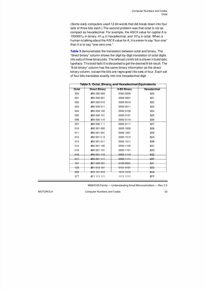
Table 3 demonstrates the translation between octal and binary. The
“direct binary” column shows the digit-by-digit translation of octal digits
into sets of three binary bits. The leftmost (ninth) bit is shown in bold italic
typeface. This bold italic 0 is discarded to get the desired 8-bit result. The
“8-bit binary” column has the same binary information as the direct
binary column, except the bits are regrouped into sets of four. Each set
of four bits translates exactly into one hexadecimal digit.
Table 3. Octal, Binary, and Hexadecimal Equivalents
Octal Direct Binary 8-Bit Binary Hexadecimal
000 0 00 000 000 0000 0000 $00
001 0 00 000 001 0000 0001 $01
002 0 00 000 010 0000 0010 $02
003 0 00 000 011 0000 0011 $03
004 0 00 000 100 0000 0100 $04
005 0 00 000 101 0000 0101 $05
006 0 00 000 110 0000 0110 $06
007 0 00 000 111 0000 0111 $07
010 0 00 001 000 0000 1000 $08
011 0 00 001 001 0000 1001 $09
012 0 00 001 010 0000 1010 $0A
013 0 00 001 011 0000 1011 $0B
014 0 00 001 100 0000 1100 $0C
015 0 00 001 101 0000 1101 $0D
016 0 00 001 110 0000 1110 $0E
017 0 00 001 111 0000 1111 $0F
101 0 01 000 001 0100 0001 $41
125 0 01 010 101 0101 0101 $55
252 0 10 101 010 1010 1010 $AA
377 0 11 111 111 1111 1111 $FF
8/2/2019 122 Textbook
http://slidepdf.com/reader/full/122-textbook 34/331
Computer Numbers and Codes
M68HC05 Family — Understanding Small Microcontrollers — Rev. 2.0
34 Computer Numbers and Codes MOTOROLA
When mentally translating octal values to binary byte values, the octal
value is represented by three octal digits. Each octal digit represents
three binary bits so there is one extra bit (3 digits × 3 bits = 9 bits). Since
Western-speaking people typically work from left to right, it is easy to
forget to throw away the leftmost extra bit from the leftmost octal digit
and end up with an extra (ninth) bit. When translating from hexadecimal
to binary, it is easier because each hexadecimal digit translates into
exactly four binary bits. Two hexadecimal digits exactly match the eight
binary bits in a byte.
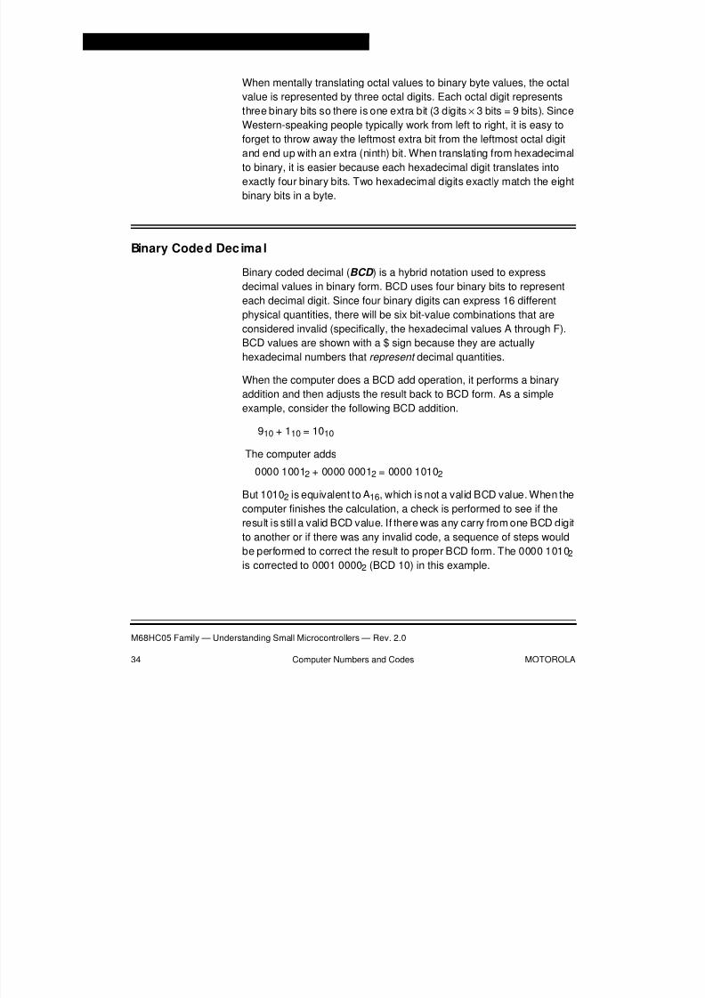
Binary Coded Dec imal
Binary coded decimal (BCD ) is a hybrid notation used to expressdecimal values in binary form. BCD uses four binary bits to represent
each decimal digit. Since four binary digits can express 16 different
physical quantities, there will be six bit-value combinations that are
considered invalid (specifically, the hexadecimal values A through F).
BCD values are shown with a $ sign because they are actually
hexadecimal numbers that represent decimal quantities.
When the computer does a BCD add operation, it performs a binary
addition and then adjusts the result back to BCD form. As a simple
example, consider the following BCD addition.
910 + 110 = 1010
The computer adds
0000 10012 + 0000 00012 = 0000 10102
But 10102 is equivalent to A16, which is not a valid BCD value. When the
computer finishes the calculation, a check is performed to see if the
result is still a valid BCD value. If there was any carry from one BCD digit
to another or if there was any invalid code, a sequence of steps wouldbe performed to correct the result to proper BCD form. The 0000 10102
is corrected to 0001 00002 (BCD 10) in this example.

8/2/2019 122 Textbook
http://slidepdf.com/reader/full/122-textbook 35/331
Computer Numbers and Codes
Binary Coded Decimal
M68HC05 Family — Understanding Small Microcontrollers — Rev. 2.0
MOTOROLA Computer Numbers and Codes 35
In most cases, using BCD notation in computer calculations is inefficient.
It is better to change from decimal to binary as information is entered, do
all computer calculations in binary, and change the binary result back to
BCD or decimal as needed for display. This is true because: First, not all
microcontrollers are capable of doing BCD calculations because they
need a digit-to-digit carry indicator that is not present on all computers
(although Motorola MCUs do have this half-carry indicator). And,
second, forcing the computer to emulate human behavior is inherently
less efficient than allowing the computer to work in its native binarysystem.
Table 4. Decimal, BCD, and Binary Equivalents
Decimal BCD BinaryHexadecimal(reference)
0 $0 0000 $0
1 $1 0001 $1
2 $2 0010 $2
3 $3 0011 $3
4 $4 0100 $4
5 $5 0101 $5
6 $6 0110 $6
7 $7 0111 $7
8 $8 1000 $8
9 $9 1001 $91010 $A
1011 $B
Invalid 1100 $C
BCD 1101 $D
Combinations 1110 $E
1111 $F
10 $10 0001 0000 $10
99 $99 1001 1001 $99

8/2/2019 122 Textbook
http://slidepdf.com/reader/full/122-textbook 36/331
Computer Numbers and Codes
M68HC05 Family — Understanding Small Microcontrollers — Rev. 2.0
36 Computer Numbers and Codes MOTOROLA
Review
Computers have two logic levels (0 and 1) so they work in the binary
numbering system. Probably because people have 10 fingers, they workin the base 10 decimal numbering system.
Hexadecimal numbers use the 16 symbols 0 through 9 and A through F.
Each hexadecimal digit can represent a set of four binary digits exactly.
Table 2 shows the decimal, binary, and hexadecimal equivalents of
various values. A $ symbol is used before a hexadecimal valueor an H
is used after a hexadecimal value to distinguish it from decimal numbers.
ASCII is a widely accepted code that allows alphanumeric information to
be represented as binary values.
Each instruction or variation of an instruction has a unique opcode
(binary value) that the CPU recognizes as a request to perform a specific
instruction. CPUs from different manufacturers have different sets of
opcodes.
Programmers specify instructions by a mnemonic such as INCA. A
computer program, called an assembler, translates mnemonic
instructions into opcodes the CPU can understand.

8/2/2019 122 Textbook
http://slidepdf.com/reader/full/122-textbook 37/331
M68HC05 Family — Understanding Small Microcontrollers — Rev. 2.0
MOTOROLA Basic Logic Elements 37
Basic Logic Elements
Contents
Introduction . . . . . . . . . . . . . . . . . . . . . . . . . . . . . . . . . . . . . . . . . . . . .37
Logic Levels. . . . . . . . . . . . . . . . . . . . . . . . . . . . . . . . . . . . . . . . . . . . .38
CMOS Transistors. . . . . . . . . . . . . . . . . . . . . . . . . . . . . . . . . . . . . . . .39
Simple Gates. . . . . . . . . . . . . . . . . . . . . . . . . . . . . . . . . . . . . . . . . . . .40
Inverter . . . . . . . . . . . . . . . . . . . . . . . . . . . . . . . . . . . . . . . . . . . . . .40NAND Gate . . . . . . . . . . . . . . . . . . . . . . . . . . . . . . . . . . . . . . . . . . .41
NOR Gate . . . . . . . . . . . . . . . . . . . . . . . . . . . . . . . . . . . . . . . . . . . .42
Transmission Gates, Buffers, and Flip Flops. . . . . . . . . . . . . . . . . . . .44
Transmission Gate . . . . . . . . . . . . . . . . . . . . . . . . . . . . . . . . . . . . .44
Three-State Buffer. . . . . . . . . . . . . . . . . . . . . . . . . . . . . . . . . . . . . .46
Half Flip Flop (HFF). . . . . . . . . . . . . . . . . . . . . . . . . . . . . . . . . . . . .48
Review. . . . . . . . . . . . . . . . . . . . . . . . . . . . . . . . . . . . . . . . . . . . . . . . .49
Introduction
Digital computers are made up of relatively simple logic elements
sometimes called gates, which are small circuits that can be connected
in various ways to manipulate logic-level signal voltages. Although this
textbook is not intended to provide detailed information on logic design,
some knowledge of the most basic logic elements will help you
understand the inner workings of microcontrollers.

8/2/2019 122 Textbook
http://slidepdf.com/reader/full/122-textbook 38/331
Basic Logic Elements
M68HC05 Family — Understanding Small Microcontrollers — Rev. 2.0
38 Basic Logic Elements MOTOROLA
This chapter begins with a close look at the requirements for logic-level
voltages. Transistors and interconnections for a typical CMOS
(complementary metal-oxide semiconductor) microcontroller are
discussed. A simple inverter, NAND gate, and NOR gate are explained.
Finally, a transmission gate, a three-state buffer, and a flip-flop circuit
are described. Virtually any part of a microcontroller can be explained in
terms of these few simple logic elements.
Logic Levels
Earlier, in the discussion of what a microcontroller is, we said a level of
approximately 0 volts indicates a logic 0 and a voltage approximately
equal to the positive power source indicates a logic 1 signal. To be moreprecise, there is a voltage level below which the microcontroller
manufacturer guarantees that a signal will be recognized as a valid
logic 0. Similarly, there is a voltage levelabove which the microcontroller
manufacturer guarantees that a signal will be recognized as a valid
logic 1. When designing a microcontroller system, be sure that all signals
conform to these specified limits, even under worst-case conditions.
Most modern microcontrollers use a technology called complementary
metal-oxide semiconductor (CMOS). This means the circuits include
both N-type and P-type transistors. Transistors will be explained ingreater detail later in this chapter.
In a typical CMOS circuit, a logic 0 input may be specified as 0.0 volts to
0.3 times VDD. If VDD is 5.0 volts, this translates to the range 0.0 to
1.5 volts. A logic 1 input may be specified as 0.7 times VDD to VDD. If
VDD is 5.0 volts, this translates to the range 3.5 to 5.0 volts.

8/2/2019 122 Textbook
http://slidepdf.com/reader/full/122-textbook 39/331
Basic Logic Elements
CMOS Transistors
M68HC05 Family — Understanding Small Microcontrollers — Rev. 2.0
MOTOROLA Basic Logic Elements 39
CMOS Transistors
Figure 3 shows the symbols for an N-type and a P-type CMOS
transistor. The exact characteristics of these transistors can bedetermined by their physical layout, size, and shape. For the purposes
of this textbook, they may be treated as simple switching devices.
Figure 3. N-Type and P-Type CMOS Transistors
The N-type transistor in Figure 3 has its source terminal [3] connected
to ground. For an N-type transistor to be on (conducting), its gate voltage
[2] must be higher than its source voltage [3] by an amount known as a
threshold. This N-type transistor is said to be on (conducts between
terminals [1] and [3]) when there is a logic 1 voltage on its gate [2]. When
the gate is at logic 0, this N-type transistor is said to be off and acts as
an open circuit between terminals [1] and [3].
The P-type transistor in Figure 3 has its source terminal [4] connectedto VDD. For a P-type transistor to be on , its gate voltage [5] must be lower
than its source voltage [4] by an amount known as a threshold. A P-type
transistor is indicated by the small opened circle at its gate [5]. When
there is a logic 0 voltage on the gate [5] of this P-type transistor, it is said
to be on and acts like there is a short circuit between terminals [4] and
[6]. When the gate is at logic 1, this P-type transistor is off and acts as
an open circuit between terminals [4] and [6].
It is relatively easy to assemble thousands of N- and P-type transistors
on a single microcontroller integrated circuit and to connect them invarious ways to perform complex logical operations. In the following
paragraphs, we look at some of the most basic logic circuits that are
found in a microcontroller.
[1][2]
[3]
[4][5]
[6]
VDD
P-TYPEN-TYPE

8/2/2019 122 Textbook
http://slidepdf.com/reader/full/122-textbook 40/331
Basic Logic Elements
M68HC05 Family — Understanding Small Microcontrollers — Rev. 2.0
40 Basic Logic Elements MOTOROLA
Simple Gates
The three most basic types of logic gates found in a microcontroller are
the inverter, the NAND gate, and the NOR gate. A logic designer usesvarious combinations of these basic gates to form more-complex logic
circuits, such as those that add two binary numbers together. While this
textbook is not intended to teach logic design techniques, these circuits
are discussed to give you a better understanding of how a
microcontroller operates on digital information.
Inverter Figure 4 shows the inverter logic symbol, a truth table for an inverter,
and a CMOS equivalent circuit. When a logic-level signal (0 or 1) is
presented to the input [1] of an inverter, the opposite logic level appearsat its output [2].
Figure 4. CMOS Inverter
Refer to the CMOS equivalent circuit at the right of Figure 4 and to
Table 5 for the following discussion: When input [1] is a logic 0, N
transistor [4] is off and P transistor [3] is on, connecting output [2] to VDD
(logic 1). When input [1] is a logic 1, P transistor [3] is off and N transistor
[4] is on, connecting output [2] to ground (logic 0).
Table 5. Inverter Gate Operation
Input[1]
Transistor Output[2][3] [4]
0 On Off Connected to VDD (1)
1 Off On Connected to ground (0)
[3]
[1]
[4]
VDD
[2]
Input[1]
Output[2]
0 1
1 0
[1] [2]

8/2/2019 122 Textbook
http://slidepdf.com/reader/full/122-textbook 41/331
Basic Logic Elements
Simple Gates
M68HC05 Family — Understanding Small Microcontrollers — Rev. 2.0
MOTOROLA Basic Logic Elements 41
NAND Gate Figure 5 shows the NAND gate logic symbol, a truth table for a CMOS
NAND gate, and a CMOS equivalent circuit. When both input [1] and
input [2] of the NAND gate are logic-level 1 signals, the output [3] will be
a logic 0. If any of the inputs to a NAND gate are logic 0s, the output will
be a logic 1.
Figure 5. CMOS NAND Gate
Refer to the CMOS equivalent circuit at the right of Figure 5 and to
Table 6 for the following discussion: When both inputs [1] and [2] are
logic 1s, P transistors [6] and [4] are both off and N transistors [5] and [7]
are both on, so output [3] is connected to ground (logic 0). When input
[1] is at logic 0, N transistor [5] is off, which disconnects output [3] from
ground regardless of the condition of N transistor [7]. Also, when input
[1] is logic 0, P transistor [4] is on, connecting output [3] to VDD (logic 1).
Similarly, when input [2] is logic 0, N transistor [7] is off, which
disconnects output [3] from ground regardless of the condition of N
transistor [5]. Also, when input [2] is logic 0, P transistor [6] is on,
connecting output [3] to VDD (logic 1).
Table 6. NAND Gate-Level Operation
Input Transistor Output
[1] [2] [6] [4] [5] [7] [3]
0 0 On On Off Off VDD (1)
0 1 Off On Off On VDD (1)
1 0 On Off On Off VDD (1)
1 1 Off Off On On GND (0)
[4]
[1]
[7]
VDD
[3]
Input Output[3][1] [2]
0 0 1
0 1 1
1 0 1
1 1 0
[1]
[2][3]
[5]
[6]
VDD
[2]

8/2/2019 122 Textbook
http://slidepdf.com/reader/full/122-textbook 42/331
Basic Logic Elements
M68HC05 Family — Understanding Small Microcontrollers — Rev. 2.0
42 Basic Logic Elements MOTOROLA
Although this is a simple logical function, it shows how CMOS transistors
can be interconnected to perform Boolean logic on simple logic-level
signals. Boolean logic is a 2-valued (0 and 1) algebraic system based on
mathematical forms and relationships, and is named for the Irish
mathematician who formulated it.
NOR Gate Figure 6 shows the logic symbol, a truth table for a CMOS NOR gate,
and a CMOS equivalent circuit. When neither input [1] nor input [2] of a
NOR gate is a logic-level 1 signal, the output [3] will be a logic 1. If any
input to a NOR gate is a logic 1, the output will be a logic 0.
Figure 6. CMOS NOR Gate
[6]
[1]
[5]
VDD
[3]
Input Output[3][1] [2]
0 0 1
0 1 0
1 0 0
1 1 0
[1]
[2][3]
[4]
[7][2]

8/2/2019 122 Textbook
http://slidepdf.com/reader/full/122-textbook 43/331
Basic Logic Elements
Simple Gates
M68HC05 Family — Understanding Small Microcontrollers — Rev. 2.0
MOTOROLA Basic Logic Elements 43
Refer to the CMOS equivalent circuit at the right of Figure 6 and to
Table 7 for the following discussion: When both inputs [1] and [2] are
logic 0s, N transistors [5] and [7] are both off and P transistors [4] and [6]
are both on, so output [3] is connected to VDD (logic 1). When input [1]
is at logic 1, P transistor [4] is off, which disconnects output [3] from VDD
regardless of the condition of P transistor [6]. Also, when input [1] is logic
1, N transistor [5] is on, connecting output [3] to ground (logic 0).
Similarly, when input [2] is logic 1, P transistor [6] is off, which
disconnects output [3] from VDD regardless of the condition of P
transistor [4]. Also when input [2] is logic 1, N transistor [7] is on,
connecting output [3] to ground (logic 0).
Table 7. NOR Gate Truth Table
Input Transistor Output
[1] [2] [4] [5] [6] [7] [3]
0 0 On Off On Off VDD (1)
0 1 On Off Off On GND (0)
1 0 Off On On Off GND (0)
1 1 Off On Off On GND (0)
8/2/2019 122 Textbook
http://slidepdf.com/reader/full/122-textbook 44/331
Basic Logic Elements
M68HC05 Family — Understanding Small Microcontrollers — Rev. 2.0
44 Basic Logic Elements MOTOROLA
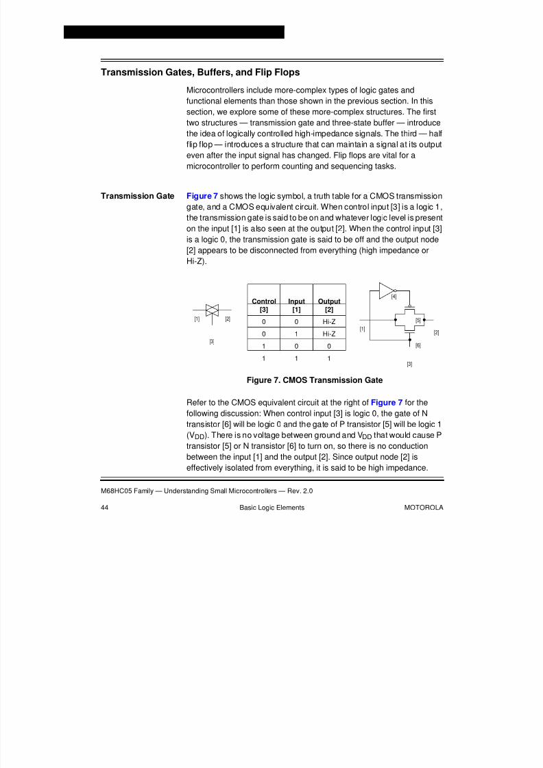
Transmission Gates, Buffers, and Flip Flops
Microcontrollers include more-complex types of logic gates and
functional elements than those shown in the previous section. In thissection, we explore some of these more-complex structures. The first
two structures — transmission gate and three-state buffer — introduce
the idea of logically controlled high-impedance signals. The third — half
flip flop — introduces a structure that can maintain a signal at its output
even after the input signal has changed. Flip flops are vital for a
microcontroller to perform counting and sequencing tasks.
Transmission Gate Figure 7 shows the logic symbol, a truth table for a CMOS transmission
gate, and a CMOS equivalent circuit. When control input [3] is a logic 1,the transmission gate is said to be on and whatever logic level is present
on the input [1] is also seen at the output [2]. When the control input [3]
is a logic 0, the transmission gate is said to be off and the output node
[2] appears to be disconnected from everything (high impedance or
Hi-Z).
Figure 7. CMOS Transmission Gate
Refer to the CMOS equivalent circuit at the right of Figure 7 for the
following discussion: When control input [3] is logic 0, the gate of Ntransistor [6] will be logic 0 and the gate of P transistor [5] will be logic 1
(VDD). There is no voltage between ground and VDD that would cause P
transistor [5] or N transistor [6] to turn on, so there is no conduction
between the input [1] and the output [2]. Since output node [2] is
effectively isolated from everything, it is said to be high impedance.
Control
[3]
Input
[1]
Output
[2]0 0 Hi-Z
0 1 Hi-Z
1 0 0
1 1 1
[1] [2]
[3]
[1]
[4]
[5]
[2]
[6]
[3]

8/2/2019 122 Textbook
http://slidepdf.com/reader/full/122-textbook 45/331
Basic Logic Elements
Transmission Gates, Buffers, and Flip Flops
M68HC05 Family — Understanding Small Microcontrollers — Rev. 2.0
MOTOROLA Basic Logic Elements 45
When control input [3] is a logic 1, the transmission gate is said to be on
and there appears to be a direct connection from the input [1] to the
output [2]. If both control [3] and input [1] are at logic 1, P transistor [5]
will be on and will form the connection between the input [1] and output
[2]. Although the gate of N transistor [6] is a logic 1, the source [1] is also
at the same voltage, so transistor [6] will be off. If control [3] is at logic 1
and input [1] is at logic 0, N transistor [6] will be on and will form the
connection between the input [1] and output [2]. Although the gate of P
transistor [5] is a logic 0, the source [1] is also at the same voltage, so
transistor [5] will be off.
The transmission gate shown in Figure 7 is sometimes called an analog
switch because it is capable of passing signals that fall between legal
digital logic levels. For this discussion, however, we are interested only
in digital logic-level signals, so we will refer to this structure as a
transmission gate.
Transmission gates can form data multiplexers, as shown in Figure 8.
When select signal [3] is a logic 1, transmission gate [6] is on and
transmission gate [7] (because of inverter [5]) is off. Thus output [4] will
have the same logic level as input [1], and signals on input [2] will not
affect output [4]. When select signal [3] is a logic 0, transmission gate [7]
is on and transmission gate [6] is off. Thus output [4] will have the same
logic level as input [2] and signals on input [1] will not affect output [4].
Figure 8. 2:1 Data Multiplexer
Select[3]
Input Output[4][1] [2]
0 0 0 0
0 0 1 1
0 1 0 0
0 1 1 1
1 0 0 0
1 0 1 0
1 1 0 1
1 1 1 1
[1]
[2]
[3]
[4]
[5]
[6]
[7]

8/2/2019 122 Textbook
http://slidepdf.com/reader/full/122-textbook 46/331
Basic Logic Elements
M68HC05 Family — Understanding Small Microcontrollers — Rev. 2.0
46 Basic Logic Elements MOTOROLA
Three-State Buffer Figure 9 shows the logic symbol, a CMOS equivalent circuit, and a truthtable for a CMOS three-state buffer. When control input [3] is a logic 0,
the buffer is said to be off and output [2] is an isolated high impedance
node. When control input [3] is a logic 1, the buffer is said to be on and
whatever logic level is present on the input [1] is also seen at the output
[2].
Figure 9. Three-State Buffer
Refer to the CMOS equivalent circuit at the right of Figure 9 and to
Table 9 for the following discussion: When control input [3] is logic 0, the
gate of N transistor [6] will be logic 0 and the gate of P transistor [5]
through inverter [9], will be logic 1 (VDD), so both transistors [5] and [6]
Table 8. Data Multiplexer Operation
Select[3]
Input Transmission Gate Output
[1] [2] [6] [7] [4]
0 0 0 Off On 0
0 0 1 Off On 1
0 1 0 Off On 0
0 1 1 Off On 1
1 0 0 On Off 0
1 0 1 On Off 0
1 1 0 On Off 1
1 1 1 On Off 1
[1] [2]
[3]
[7]
[3]
VDD
[2][1]
[9][5]
[6]
[8]
[4]Control
[3]Input
[1]Output
[2]
0 0 Hi-Z
0 1 Hi-Z
1 0 0
1 1 1
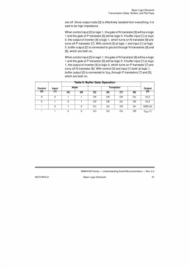
8/2/2019 122 Textbook
http://slidepdf.com/reader/full/122-textbook 47/331
Basic Logic Elements
Transmission Gates, Buffers, and Flip Flops
M68HC05 Family — Understanding Small Microcontrollers — Rev. 2.0
MOTOROLA Basic Logic Elements 47
are off. Since output node [2] is effectively isolated from everything, it is
said to be high impedance.
When control input [3] is logic 1, the gate of N transistor [6] will be a logic
1 and the gate of P transistor [5] will be logic 0. If buffer input [1] is logic0, the output of inverter [4] is logic 1, which turns on N transistor [8] and
turns off P transistor [7]. With control [3] at logic 1 and input [1] at logic
0, buffer output [2] is connected to ground through N transistors [6] and
[8], which are both on.
When control input [3] is logic 1, the gate of N transistor [6] will be a logic
1 and the gate of P transistor [5] will be logic 0. If buffer input [1] is logic
1, the output of inverter [4] is logic 0, which turns on P transistor [7] and
turns off N transistor [8]. With control [3] and input [1] both at logic 1,
buffer output [2] is connected to VDD through P transistors [7] and [5],which are both on.
Table 9. Buffer Gate Operation
Control[3]
Input[1]
Node Transistor Output[2][4] [9] [5] [6] [7] [8]
0 0 1 1 Off Off Off On Hi-Z
0 1 0 1 Off Off On Off Hi-Z
1 0 1 0 On On Off On GND (0)
1 1 0 0 On On On Off VDD (1)
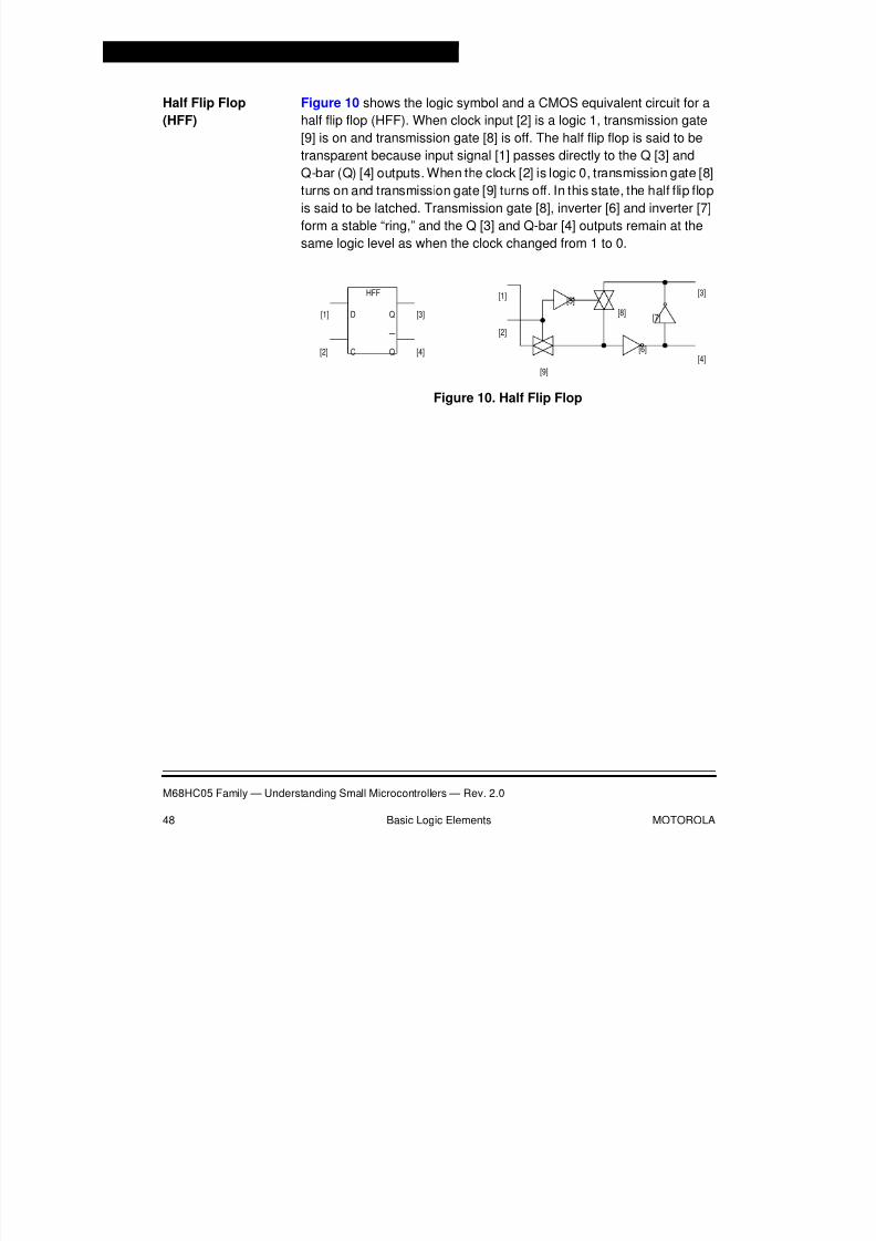
8/2/2019 122 Textbook
http://slidepdf.com/reader/full/122-textbook 48/331
Basic Logic Elements
M68HC05 Family — Understanding Small Microcontrollers — Rev. 2.0
48 Basic Logic Elements MOTOROLA
Half Flip Flop
(HFF)
Figure 10 shows the logic symbol and a CMOS equivalent circuit for a
half flip flop (HFF). When clock input [2] is a logic 1, transmission gate
[9] is on and transmission gate [8] is off. The half flip flop is said to be
transparent because input signal [1] passes directly to the Q [3] and
Q-bar (Q) [4] outputs. When the clock [2] is logic 0, transmission gate [8]
turns on and transmission gate [9] turns off. In this state, the half flip flop
is said to be latched. Transmission gate [8], inverter [6] and inverter [7]
form a stable “ring,” and the Q [3] and Q-bar [4] outputs remain at the
same logic level as when the clock changed from 1 to 0.
Figure 10. Half Flip Flop
[1]
[2]
[3]
[4]
[5]
[6]
[7][8]
[9]
[3]
[4]
[1]
[2]
D
C
Q
Q
HFF

8/2/2019 122 Textbook
http://slidepdf.com/reader/full/122-textbook 49/331
Basic Logic Elements
Review
M68HC05 Family — Understanding Small Microcontrollers — Rev. 2.0
MOTOROLA Basic Logic Elements 49
Review
Although we often think about logic levels being 0 volts or 5 volts, they
are actually ranges of voltages that are guaranteed by the MCUmanufacturer. For a specific MCU operating with VDD equal to 5.0 volts,
a logic 0 could be 0.0 to 1.5 volts and a logic 1 might be 3.5 to 5.0 volts.
Always refer to the data sheets for the MCU you are using to obtain the
voltage ranges of logic 0 and logic 1.
CMOS MCUs are made up of thousands of N-type and P-type
transistors. An N transistor is on (conducts from source to drain) when
its gate is at a logic 1 and its source is at logic 0. A P transistor is on when
its source is at logic 1 and its gate is at logic 0.
N and P transistors can be connected in various ways to perform logical
operations. Inverters, NAND gates, and NOR gates are three types of
simple logic gates. The output of an inverter is always the opposite logic
level of its input. The output of a NAND gate is logic 0 when all of its
inputs are logic 1s. The output of a NOR gate is a logic 0 when any or all
of its inputs are logic 1s.
The output of a transmission gate or a three-state buffer can be logic 0,
logic 1, or high impedance. An output is high impedance when it appears
to be not connected to anything (an open circuit).
Ahalf flip flop (HFF) has a transparent condition and a latched condition.
In the transparent condition (clock input equals logic 1), the Q output is
always equal to the logic level presented at the input. In the latched
condition (clock input equals logic 0), the output maintains the logic level
that was present when the flip flop was last in the transparent condition.
Changes in the input logic level, while the flip flop is latched, do not affect
the output logic level.

8/2/2019 122 Textbook
http://slidepdf.com/reader/full/122-textbook 50/331
Basic Logic Elements
M68HC05 Family — Understanding Small Microcontrollers — Rev. 2.0
50 Basic Logic Elements MOTOROLA
8/2/2019 122 Textbook
http://slidepdf.com/reader/full/122-textbook 51/331
M68HC05 Family — Understanding Small Microcontrollers — Rev. 2.0
MOTOROLA Computer Memory and Parallel I/O 51
Computer Memory and Parallel I/ O
Contents
Introduction . . . . . . . . . . . . . . . . . . . . . . . . . . . . . . . . . . . . . . . . . . . . .51
Pigeon Hole Analogy. . . . . . . . . . . . . . . . . . . . . . . . . . . . . . . . . . . . . .52
How a Computer Sees Memory . . . . . . . . . . . . . . . . . . . . . . . . . . . . .53
Kilobytes, Megabytes, and Gigabytes . . . . . . . . . . . . . . . . . . . . . . . . .54
Kinds of Memory . . . . . . . . . . . . . . . . . . . . . . . . . . . . . . . . . . . . . . . . .54Random Access Memory (RAM). . . . . . . . . . . . . . . . . . . . . . . . . . .55
Read-Only Memory (ROM) . . . . . . . . . . . . . . . . . . . . . . . . . . . . . . . 55
Programmable ROM (PROM) . . . . . . . . . . . . . . . . . . . . . . . . . . . . . 55
EPROM. . . . . . . . . . . . . . . . . . . . . . . . . . . . . . . . . . . . . . . . . . . .55
OTP. . . . . . . . . . . . . . . . . . . . . . . . . . . . . . . . . . . . . . . . . . . . . . .56
EEPROM . . . . . . . . . . . . . . . . . . . . . . . . . . . . . . . . . . . . . . . . . .56
I/O as a Memory Type. . . . . . . . . . . . . . . . . . . . . . . . . . . . . . . . . . .57
Internal Status and Control Registers . . . . . . . . . . . . . . . . . . . . . . .59
Memory Maps . . . . . . . . . . . . . . . . . . . . . . . . . . . . . . . . . . . . . . . . . . .60Memory Peripherals . . . . . . . . . . . . . . . . . . . . . . . . . . . . . . . . . . . . . .62
Review. . . . . . . . . . . . . . . . . . . . . . . . . . . . . . . . . . . . . . . . . . . . . . . . .62
Introduction
Before the operation of a CPU can be discussed in detail, some
conceptual knowledge of computer memory is required. In many
beginning programming classes, memory is presented as being similarto a matrix of pigeon holes where you can save messages and other
information. The pigeon holes we refer to here are like the mailboxes in
a large apartment building. This is a good analogy, but it needs a little
refinement to explain the inner workings of a CPU.

8/2/2019 122 Textbook
http://slidepdf.com/reader/full/122-textbook 52/331
Computer Memory and Parallel I/ O
M68HC05 Family — Understanding Small Microcontrollers — Rev. 2.0
52 Computer Memory and Parallel I/O MOTOROLA
Pigeon Hole Analogy
The whole idea of any type of memory is to save information. Of course,
there is no point in saving information if you don’t have a reliable way torecall that information when it’s needed. The array of mailboxes in a
large apartment building could be used as a type of memory storage.
You could put information into a mail box with a certain apartment
number on it. When you wanted to recall that information, you could go
to the mailbox with that address and retrieve the information.
Next, we will carry this analogy further to explain just how a computer
sees memory. We will confine our discussion to an 8-bit computer so
that we can be very specific.
In an 8-bit CPU, each pigeon hole (or mailbox) can be thought of as
containing a set of eight on/off switches. Unlike a real pigeon hole, you
cannot fit more information in by writing smaller, and there is no such
thing as an empty pigeon hole (the eight switches are either on or off).
The contents of a memory location can be unknown or undefined at a
given time, just as the switches in the pigeon holes may be in an
unknown state until you set them the first time. The eight switches would
be in a row where each switch represents a single binary digit (bit). A
binary 1 corresponds to the switch being on, and a binary 0 corresponds
to the switch being off. Each pigeon hole (memory location) has a uniqueaddress so that information can be stored and reliably retrieved.

8/2/2019 122 Textbook
http://slidepdf.com/reader/full/122-textbook 53/331
Computer Memory and Parallel I/O
How a Computer Sees Memory
M68HC05 Family — Understanding Small Microcontrollers — Rev. 2.0
MOTOROLA Computer Memory and Parallel I/O 53
In an apartment building, the addresses of the mailboxes might be
100–175 for the first floor, 200–275 for the second floor, etc. These are
decimal numbers that have meaning for people. As we discussed earlier,
computers work in the binary number system. A computer with four
address wires could uniquely identify 16 addressesbecause a set of four
1s and 0s can be arranged in 16 different combinations. This computer
would identify the addresses of the 16 memory locations (mailboxes)
with the hexadecimal values $0 through $F.
In the smallest MC68HC05 microcontrollers, their 10 address lines allow
these computers to address 1024 unique memory locations. In
comparison, the MC68HC11 general-purpose 8-bit microcontroller has
16 address lines, which means it can address 65,536 unique memory
locations.
How a Computer Sees Memory
An 8-bit computer with 10 address lines sees memory as a continuous
row of 1024, 8-bit values. The first memory location has the address
00 0000 00002 and the last location has the address 11 1111 11112.
These 10-bit addresses are normally expressed as two 8-bit numbers
that are in turn expressed as four hexadecimal digits. In hexadecimal
notation, these addresses would range from $0000 to $03FF.
The computer specifies which memory location is being accessed (read
from or written to) by putting a unique combination of 1s and 0s on the
10 address lines. The intention to read the location or write to the
location is signalled by placing a 1 (read) or a 0 (write) on a line called
read/write (R/W). The information from or for the memory location is
carried on eight data lines.
To a computer any memory location can be written to or read from. Not
all memory types are writable, but it is the job of the programmer to knowthis, not the computer. If a programmer erroneously instructs the
computer to write to a read-only memory, it will try to do so.
8/2/2019 122 Textbook
http://slidepdf.com/reader/full/122-textbook 54/331
Computer Memory and Parallel I/ O
M68HC05 Family — Understanding Small Microcontrollers — Rev. 2.0
54 Computer Memory and Parallel I/O MOTOROLA
Kilobytes, Megabytes, and Gigabytes
The smallest unit of computer memory is a single bit that can store one
value of 0 or 1. These bits are grouped into sets of eight bits to make onebyte . Larger computers further group bits into sets of 16 or 32 to make
a unit called a word . The size of a word can be different for different
computers.
In the decimal world, we sometimes express very small or very large
numbers by including a prefix such as milli, kilo, etc., before the unit of
measure. In the binary world, we use similar prefixes to describe large
amounts of memory. In the decimal system, the prefix kilo means 1000
(or 103) times a value. In the binary system, the integer power of 2 that
comes closest to 100010 is 210
= 102410. We say kilobytes but we meanKbytes which are multiples of 102410 bytes. Although this is sloppy
scientific terminology, it has become a standard through years of use.
A megabyte is 220 or 1,048,57610 bytes. A gigabyte is 230 or
1,073,741,82410 bytes. A personal computer with 32 address lines can
theoretically address 4 gigabytes (4,294,967,29610) of memory. The
small microcontrollers discussed in this textbook have only about 512
bytes to 16 kilobytes of memory.
Kinds of Memory
Computers use several kinds of information that require different kinds
of memory. The instructions that control the operation of a
microcontroller are stored in a non-volatile memory so the system does
not have to be reprogrammed after power has been off. Working
variables and intermediate results need to be stored in a memory that
can be written quickly and easily during system operation. It is not
important to remember this kind of information when there is no power,so a volatile form of memory can be used. These types of memory are
changed (written) and read only by the CPU in the computer.
Like other memory information, input data is read by the CPU and output
data is written by the CPU. I/O (input/output) and control registers are

8/2/2019 122 Textbook
http://slidepdf.com/reader/full/122-textbook 55/331
Computer Memory and Parallel I/O
Kinds of Memory
M68HC05 Family — Understanding Small Microcontrollers — Rev. 2.0
MOTOROLA Computer Memory and Parallel I/O 55
also a form of memory to the computer, but they are different than other
kinds of memory because the information can be sensed and/or
changed by something other than the CPU.
Random Access
Memory (RAM)
RAM is a volatile form of memory that can be read or written by the CPU.
As its name implies, RAM locations may be accessed in any order. This
is the most common type of memory in a personal computer. RAM
requires a relatively large amount of area on an integrated circuit chip.
Because of the relatively large chip area (and thus higher cost), usually
only small amounts of RAM are included in microcontroller chips.
Read-Only
Memory (ROM)
ROM gets its information during the manufacturing process. The
information must be provided by the customer before the integrated
circuit, that will contain this information, is made. When the finished
microcontroller is used, this information can be read by the CPU but
cannot be changed. ROM is considered a non-volatile memory because
the information does not change if power is turned off. ROM is the
simplest, smallest, and least expensive type of non-volatile memory.
Programmable
ROM (PROM)
PROM is similar to ROM except that it can be programmed after the
integrated circuit is made. Some variations of PROM include:
• Erasable PROM (EPROM )
• One-time-programmable PROM (OTP )
• Electrically erasable PROM (EEPROM )
EPROM EPROM can be erased by exposing it to an ultraviolet light source.
Microcontrollers with EPROM that can be erased have a small quartz
window that allows the integrated circuit chip inside to be exposed to the
ultraviolet light. The number of times an EPROM can be erased andreprogrammed is limited to a few hundred cycles, depending on the
particular device.
A special procedure is used to program information into an EPROM
memory. Most EPROM microcontrollers also use an additional power

8/2/2019 122 Textbook
http://slidepdf.com/reader/full/122-textbook 56/331
Computer Memory and Parallel I/ O
M68HC05 Family — Understanding Small Microcontrollers — Rev. 2.0
56 Computer Memory and Parallel I/O MOTOROLA
supply, such as +12 Vdc, during the EPROM programming operation.
The CPU cannot simply write information to an EPROM location the way
it would write to a RAM location.
Some microcontrollers have built-in EPROM programming circuits sothat the CPU in the microcontroller can program EPROM locations.
When the EPROM is being programmed, it is not connected to the
address and data buses the way a normal memory would be. In the
pigeon hole analogy, this would be like removing the entire rack of
mailboxes and taking it to a warehouse where the boxes would be filled
with information. While the mailboxes are away being programmed, the
people at the apartment building cannot access the mailboxes.
Some EPROM microcontrollers (not the MC68HC705J1A) have a
special mode of operation that makes them appear to be an industrystandard EPROM memory. These devices can be programmed with a
general-purpose commercial EPROM programmer.
OTP When an EPROM microcontroller is packaged in an opaque plastic
package, it is called a one-time programmable or OTP microcontroller.
Since ultraviolet light cannot pass through the package, the memory
cannot be erased. The integrated circuit chip inside an OTP MCU is
identical to that in the quartz window package. The plastic package is
much less expensive than a ceramic package with a quartz window.OTP MCUs are ideal for quick turn around, first production runs, and low
volume applications.
EEPROM EEPROM can be erased electrically by commands in a microcontroller.
To program a new value into a location, you must first erase the location
and then perform a series of programming steps. This is somewhat more
complicated than changing a RAM location that can simply be written to
a new value by the CPU. The advantage of EEPROM is that it is a
non-volatile memory. EEPROM does not lose its contents when power
is turned off. Unlike RAM memory, the number of times you can erase
and reprogram an EEPROM location is limited (typically to 10,000
cycles). The number of times you can read an EEPROM location is not
limited.

8/2/2019 122 Textbook
http://slidepdf.com/reader/full/122-textbook 57/331
Computer Memory and Parallel I/O
Kinds of Memory
M68HC05 Family — Understanding Small Microcontrollers — Rev. 2.0
MOTOROLA Computer Memory and Parallel I/O 57
I/O as a Memory
Type
I/O status and control information is a type of memory location that
allows the computer system to get information to or from the outside
world. This type of memory location is unusual because the information
can be sensed and/or changed by something other than the CPU.
The simplest kinds of I/O memory locations are basic input ports and
output ports. In an 8-bit MCU, a simple input port consists of eight pins
that can be read by the CPU. A simple output port consists of eight pins
that the CPU can control (write to). In practice, a simple output port
location is usually implemented with eight latches and feedback paths
that allow the CPU to read back what was previously written to the
address of the output port.
Figure 11 shows the equivalent circuits for one bit of RAM, one bit of an
input port, and one bit of a typical output port having read-backcapability. In a real MCU, these circuits would be repeated eight times to
make a single 8-bit RAM location, input port, or output port. The half flip
flops (HFF) in Figure 11 are very simple transparent flip flops. When the
clock signal is high, data passes freely from the D input to the Q and
Q-bar outputs. When the clock input is low, data is latched at the Q and
Q-bar outputs.
When the CPU stores a value to the address that corresponds to the
RAM bit in Figure 11 (a), the WRITE signal is activated to latch the data
from the data bus line into the flip flop [1]. This latch is static andremembers the value written until a new value is written to this location
or power is removed. When the CPU reads the address of this RAM bit,
the READ signal is activated, which enables the multiplexer at [2]. This
multiplexer couples the data from the output of the flip flop onto the data
bus line. In a real MCU, RAM bits are much simpler than shown here,
but they are functionally equivalent to this circuit.
When the CPU reads the address of the input port shown in Figure 11
(b), the READ signal is activated, which enables the multiplexer at [3].
The multiplexer couples the buffered data from the pin onto the data busline. A write to this address would have no meaning.

8/2/2019 122 Textbook
http://slidepdf.com/reader/full/122-textbook 58/331
Computer Memory and Parallel I/ O
M68HC05 Family — Understanding Small Microcontrollers — Rev. 2.0
58 Computer Memory and Parallel I/O MOTOROLA
Figure 11. Memory and I/O Circuitry
When the CPU stores a value to the address that corresponds to the
output port in Figure 11 (c), the WRITE signal is activated to latch the
data from the data bus line into the half flip flop [4]. The output of this
latch, which is buffered by the buffer driver at [5], appears as a digital
level on the output pin. When the CPU reads the address of this output
port, the READ signal is activated, which enables the multiplexer at [6].
This multiplexer couples the data from the output of the half flip flop ontothe data bus line.
(c) Output Port with Read-Back
HFF
D
C
Q DIGITALOUTPUT
PIN
READ
WRITE
[6]
[4]
Q
DATA BIT n
(n = 0, 1. . .or 7)
BUFFER – DRIVER
[5]
(b) Input Port Bit
DIGITAL
INPUTPIN
READ[3]
DATA BIT n
(n = 0, 1. . .or 7)
BUFFER
(a) RAM Bit
HFF
D
C
Q
READ
WRITE
[2]
[1]Q
DATA BIT n(n = 0, 1. . .or 7)

8/2/2019 122 Textbook
http://slidepdf.com/reader/full/122-textbook 59/331
Computer Memory and Parallel I/O
Kinds of Memory
M68HC05 Family — Understanding Small Microcontrollers — Rev. 2.0
MOTOROLA Computer Memory and Parallel I/O 59
Internal Status and
Control Registers
Internal status and control registers are just specialized versions of I/O
memory locations. Instead of sensing and controlling external pins,
status and control registers sense and control internal logic level signals.
Look at Figure 11 and compare the RAM bit to the output port. The onlydifference is that the output bit has a buffer to connect the state of the
half flip flop to an external pin. In the case of an internal control bit, the
buffer output is connected to some internal control signal rather than an
external pin. An internal status bit is like an input port bit except that the
signal that is sensed during a read is an internal signal rather than an
external pin.
M68HC05 microcontrollers include general-purpose parallel I/O pins.
The direction of each pin is programmable by a software-accessible
control bit. Figure 12 shows the logic for a bidirectional I/O pin, includingan output port latch and a data direction control bit.
A port pin is configured as an output if its corresponding DDR (data
direction register) bit is set to a logic 1. A pin is configured as an input if
its corresponding DDR bit is cleared to a logic 0. At power-on or reset,
all DDR bits are cleared, which configure all port pins as inputs. The
DDRs are capable of being written to or being read by the processor.
Figure 12. I/O Port with Data Direction Control
HFF
D
C
QDIGITAL
I/OPIN
READ
PORT
WRITE
PORT
Q
DATA BIT n
(n = 0, 1. . .or 7)
BUFFER – DRIVER
BUFFER
HFF
D
C
Q
READDDR BIT
WRITEDDR BIT
Q

8/2/2019 122 Textbook
http://slidepdf.com/reader/full/122-textbook 60/331
Computer Memory and Parallel I/ O
M68HC05 Family — Understanding Small Microcontrollers — Rev. 2.0
60 Computer Memory and Parallel I/O MOTOROLA
Memory Maps
Since there are a thousand or more memory locations in an MCU
system, it is important to have a convenient way to keep track of wherethings are. A memory map is a pictorial representation of the total MCU
memory space. Figure 14 is a typical memory map showing the memory
resources in the MC68HC705J1A.
The 4-digit hexadecimal values along the left edge of Figure 14 are
addresses beginning with $0000 at the top and increasing to $07FF at
the bottom. $0000 corresponds to the first memory location (selected
when the CPU drives all address lines of the internal address bus to logic
0). $07FF corresponds to the last memory location selected (when the
CPU drives all 11 address lines of the internal address bus to logic 1).The labels within the vertical rectangle identify what kind of memory
(RAM, EPROM, I/O registers, etc.) resides in a particular area of
memory.
Some areas, such as I/O registers, need to be shown in more detail
because it is important to know the names of each individual location.
The whole vertical rectangle can be interpreted as a row of 2048 pigeon
holes (memory locations). Each of these 2048 memory locations
contains eight bits of data as shown in Figure 13.
Figure 13. Expanded Detail of One Memory Location
The first 256 memory locations ($0000–$00FF) can be accessed by the
computer in a special way called direct addressing mode. Addressing
modes are discussed in greater detail in M68HC05 Instruction Set. Indirect addressing mode, the CPU assumes that the upper two
hexadecimal digits of address are 0; thus, only the two low-order digits
of the address need to be explicitly given in the instruction. On-chip I/O
registers and 64 bytes of RAM are located in the $0000–$00FF area of
memory.
$04PORT A DATA DIRECTION REGISTER
DDRA7 DDRA6 DDRA5 DDRA4 DDRA3 DDRA2 DDRA1 DDRA0
BIT 7 BIT 6 BIT 5 BIT 4 BIT 3 BIT 2 BIT 1 BIT 0

8/2/2019 122 Textbook
http://slidepdf.com/reader/full/122-textbook 61/331
Computer Memory and Parallel I/O
Memory Maps
M68HC05 Family — Understanding Small Microcontrollers — Rev. 2.0
MOTOROLA Computer Memory and Parallel I/O 61
Figure 14. Typical Memory Map
$0000
$001F$0020
$00BF$00C0
$00FF$0100
$02FF$0300
$07CF$07D0
$07FF
I/O32 Bytes
Unused160 Bytes
Unused512 Bytes
User EPROM1232 Bytes
User & StackRAM
64 Bytes
Port B Data Register $01
$02
$03
$04
$05
$06
$07
$08
$09
$0A
$0B
$0C
$0D
$0E
$0F
$10
$11$12
$13
$14
$15
$16
$17
$18
$19
$1A
$1B
$1C
$1D
$1EReserved $1F
COP Register $07F0
Mask Option Register $07F1
Reserved $07F7
$07F8
$07F9
$07FA
$07FB$07FC
$07FD
RESET Vector (High Byte) $07FE
RESET Vector (Low Byte) $07FF
Test ROM — 2 Bytes
User Vectors(EPROM)16 Bytes
$07EE$07EF$07F0
Port A Data Register $00
Unused
Unused
Unused
Unused
Unused
Unused
EPROM Programming Register
Unused
Unused
Unused
Unused
Unused
UnusedPort B Pulldown Register
Port A Pulldown Register
Unused
Unused
Unused
Unused
Unused
IRQ Status & Control Register
Timer Counter Register
Timer Status & Control
Unused
Unused
Port B Data Direction Register
Port A Data Direction Register
Unused
Unused
SWI Vector (High Byte)
SWI Vector (Low Byte)
IRQ Vector (High Byte)
IRQ Vector (Low Byte)
Timer Vector (High Byte)
Timer Vector (Low Byte)
$07ED
Unimplemented30 Bytes
$07F2Reserved
See Figure 13

8/2/2019 122 Textbook
http://slidepdf.com/reader/full/122-textbook 62/331
Computer Memory and Parallel I/ O
M68HC05 Family — Understanding Small Microcontrollers — Rev. 2.0
62 Computer Memory and Parallel I/O MOTOROLA
In the memory map (Figure 14), the expansion of the I/O area of
memory identifies each register location with the two low-order digits of
its address rather than the full 4-digit address. For example, the 2-digit
hexadecimal value $00 appears to the right of the port A data register,
which is actually located at address $0000 in the memory map.
Memory Peripherals
Memories can be a form of peripheral. The uses for different types of
memory were discussed earlier, but the logic required to support these
memories was not considered. ROM and RAM memories are
straightforwardand require no support logic — other than address-select
logic — to distinguish one location from another. This select logic isprovided on the same chip as the memory itself.
EPROM (erasable PROM) and EEPROM (electrically erasable PROM)
memories require support logic for programming (and erasure in the
case of EEPROM). For example, the peripheral support logic in the
MC68HC705J1A is like having a PROM programmer built into the MCU.
A control register includes control bits to select between programming
and reading modes and to enable the high-voltage programming power
supply.
Review
We can think of computer memory as an array of mailboxes, but a
computer views memory as a series of 8-bit values.
If a computer has n address lines, it can uniquely address 2n memory
locations. A computer with 11 address lines can address 211, or 204810
locations.
NOTE: One kilobyte (written 1 Kbyte) is equal to 1024 10 bytes.
Kinds of Memory

8/2/2019 122 Textbook
http://slidepdf.com/reader/full/122-textbook 63/331
Computer Memory and Parallel I/O
Review
M68HC05 Family — Understanding Small Microcontrollers — Rev. 2.0
MOTOROLA Computer Memory and Parallel I/O 63
• RAM — Random access memory can be read or written by a
CPU. Contents are remembered as long as power is applied.
• ROM — Read-only memory can be read but not changed. The
contents must be determined before the integrated circuit ismanufactured. Power is not required for ROM to remember its
contents.
• EPROM — Erasable programmable ROM can be changed by
erasing it with an ultraviolet light and then programming it with a
new value. The erasure and programming operations can be
performed a limited number of times after the integrated circuit is
manufactured. Power is not required for EPROM to remember its
contents.
• OTP — The chip in a one-time-programmable EPROM is identicalto that in an EPROM, but it is packaged in an opaque package.
Since ultraviolet light cannot get through the package, this
memory cannot be erased after it is programmed.
• EEPROM — Electrically erasable PROM can be changed using
electrical signals and remembers its contents even when no
power is applied. Typically, an EEPROM location can be erased
and reprogrammed up to 10,000 times before it wears out.
• I/O — I/O, control, and status registers are a special kind of
memory because the information can be sensed and/or changedby something other than the CPU.
• Non-Volatile Memory — Non-volatile memory remembers its
contents even when there is no power.
• Volatile Memory — Volatile memory forgets its contents when
power is turned off.
NOTE: Memory Map — A memory map is a pictorial view of all of the memory
locations in a computer system.
The first 256 locations in a microcontroller system can be accessed in a
special way called direct addressing mode . In direct addressing mode,
the CPU assumes the high order byte of the address is $00 so it does
not have to be explicitly given in a program (saving the space it would

8/2/2019 122 Textbook
http://slidepdf.com/reader/full/122-textbook 64/331
Computer Memory and Parallel I/ O
M68HC05 Family — Understanding Small Microcontrollers — Rev. 2.0
64 Computer Memory and Parallel I/O MOTOROLA
have taken and eliminating the clock cycle it would have required to
fetch it).
Specialty memories such as EPROM and EEPROM can be considered
peripherals in a computer system. Support circuitry and programmingcontrols are required to modify the contents of these memories. This
differs from simple memories such as RAM that can be read or written in
a single CPU clock cycle.

8/2/2019 122 Textbook
http://slidepdf.com/reader/full/122-textbook 65/331
M68HC05 Family — Understanding Small Microcontrollers — Rev. 2.0
MOTOROLA Computer Architecture 65
Computer Architecture
Contents
Introduction . . . . . . . . . . . . . . . . . . . . . . . . . . . . . . . . . . . . . . . . . . . . .66
Computer Architecture. . . . . . . . . . . . . . . . . . . . . . . . . . . . . . . . . . . . .66
CPU Registers. . . . . . . . . . . . . . . . . . . . . . . . . . . . . . . . . . . . . . . . . . .67
Timing . . . . . . . . . . . . . . . . . . . . . . . . . . . . . . . . . . . . . . . . . . . . . . . . .69
CPU View of a Program . . . . . . . . . . . . . . . . . . . . . . . . . . . . . . . . . . .70
CPU Operation . . . . . . . . . . . . . . . . . . . . . . . . . . . . . . . . . . . . . . . . . .73
Detailed Operation of CPU Instructions . . . . . . . . . . . . . . . . . . . . .73
Store Accumulator (Direct Addressing Mode). . . . . . . . . . . . . . .74
Load Accumulator (Immediate Addressing Mode) . . . . . . . . . . .75
Conditional Branch . . . . . . . . . . . . . . . . . . . . . . . . . . . . . . . . . . .76
Subroutine Calls and Returns. . . . . . . . . . . . . . . . . . . . . . . . . . .76
Playing Computer . . . . . . . . . . . . . . . . . . . . . . . . . . . . . . . . . . . . . . . .80
Resets . . . . . . . . . . . . . . . . . . . . . . . . . . . . . . . . . . . . . . . . . . . . . . . . .86
RESET Pin . . . . . . . . . . . . . . . . . . . . . . . . . . . . . . . . . . . . . . . . . . .86
Power-On Reset . . . . . . . . . . . . . . . . . . . . . . . . . . . . . . . . . . . . . . .86
Watchdog Timer Reset . . . . . . . . . . . . . . . . . . . . . . . . . . . . . . . . . .87
Illegal Address Reset . . . . . . . . . . . . . . . . . . . . . . . . . . . . . . . . . . .87
Interrupts . . . . . . . . . . . . . . . . . . . . . . . . . . . . . . . . . . . . . . . . . . . . . . .88
External Interrupts. . . . . . . . . . . . . . . . . . . . . . . . . . . . . . . . . . . . . .91
On-Chip Peripheral Interrupts . . . . . . . . . . . . . . . . . . . . . . . . . . . . . 92
Software Interrupt (SWI) . . . . . . . . . . . . . . . . . . . . . . . . . . . . . . . . . 92
Interrupt Latency . . . . . . . . . . . . . . . . . . . . . . . . . . . . . . . . . . . . . . .92
Nested Interrupts. . . . . . . . . . . . . . . . . . . . . . . . . . . . . . . . . . . . . . .93
Review. . . . . . . . . . . . . . . . . . . . . . . . . . . . . . . . . . . . . . . . . . . . . . . . .94

8/2/2019 122 Textbook
http://slidepdf.com/reader/full/122-textbook 66/331
Computer Architecture
M68HC05 Family — Understanding Small Microcontrollers — Rev. 2.0
66 Computer Architecture MOTOROLA
Introduction
This chapter takes us into the very heart of a computer to see what
makes it work. This will be a more detailed look than you normally needto use an MCU, but it will help you understand why some things are done
in a certain way.
Everything the CPU does is broken down into sequences of simple
steps. For instance, a clockoscillator generates a CPU clock that is used
to step the CPU through these sequences. The CPU clock is very fast in
human terms, so things seem to be happening almost instantaneously.
By going through these sequences step by step, you will gain a working
understanding of how a computer executes programs. You will also gain
valuable knowledge of a computer’s capabilities and limitations.
Computer Architecture
Motorola M68HC05 and M68HC11 8-bit MCUs have a specific
organization that is called a Von Neumann architecture after an
American mathematician of the same name. In this architecture, a CPU
and a memory array are interconnected by an address bus and a data
bus. The address bus is used to identify which memory location is beingaccessed, and the data bus is used to convey information either from
the CPU to the memory location (pigeon hole) or from the memory
location to the CPU.
In the Motorola implementation of this architecture, there are a few
special pigeon holes (called CPU registers) inside the CPU, which actas
a small scratch pad and control panel for the CPU. These CPU registers
are similar to memory, in that information can be written into them and
remembered. However, it is important to remember that these registers
are directly wired into the CPU and are not part of the addressablememory available to the CPU.
All information (other than the CPU registers) accessible to the CPU is
envisioned (by the CPU) to be in a single row of a thousand or more
pigeonholes.This organization is sometimescalleda memory-mapped

8/2/2019 122 Textbook
http://slidepdf.com/reader/full/122-textbook 67/331
Computer Architecture
Computer Architecture
M68HC05 Family — Understanding Small Microcontrollers — Rev. 2.0
MOTOROLA Computer Architecture 67
I/O system because the CPU treats all memory locations alike whether
they contain program instructions, variable data, or input-output (I/O)
controls. There are other computer architectures, but this textbook is not
intended to explore those variations.
Fortunately, the Motorola M68HC05 architecture we are discussing here
is one of the easiest to understand and use. This architecture
encompasses the most important ideas of digital binary computers; thus,
the information presented in this textbook will be applicable even if you
go on to study other architectures.
The number of wires in the address bus determines the total possible
number of pigeon holes; the number of wires in the data bus determines
the amount of information that can be stored in each pigeon hole.
In the MC68HC705J1A, for example, the address bus has 11 lines,
making a maximum of 2048 separate pigeon holes (in MCU jargon you
would say this CPU can access 2-K locations). Since the data bus in the
MC68HC705J1A is eight bits, each pigeon hole can hold one byte of
information. One byte is eight binary digits, or two hexadecimal digits, or
one ASCII character, or a decimal value from 0 to 255.
CPU Registers Different CPUs have different sets of CPU registers. The differences are
primarily the number and size of the registers. Figure 15 shows the CPUregisters found in an M68HC05. While this is a relatively simple set of
CPU registers, it is representative of all types of CPU registers and can
be used to explain all of the fundamental concepts. This chapter
provides a brief description of the M68HC05 registers as an introduction
to CPU architecture in general. M68HC05 Instruction Set addresses
the instruction set of the M68HC05 and includes more detailed
information about M68HC05 registers.

8/2/2019 122 Textbook
http://slidepdf.com/reader/full/122-textbook 68/331
Computer Architecture
M68HC05 Family — Understanding Small Microcontrollers — Rev. 2.0
68 Computer Architecture MOTOROLA
Figure 15. M68HC05 CPU Registers
The A register, an 8-bit scratch-pad register, is also called an
accumulator because it is often used to hold one of the operands or the
result of an arithmetic operation.
The X register is an 8-bit index register, which can also serve as a simple
scratch pad. The main purpose of an index register is to point at an areain memory where the CPU will load (read) or store (write) information.
Sometimes an index register is called a pointer register . We will learn
more about index registers when we discuss indexed addressing
modes.
The program counter (PC) register is used by the CPU to keep track of
the address of the next instruction to be executed. When the CPU is
reset (starts up), the PC is loaded from a specific pair of memory
locations called the reset vector . The reset vector locations contain the
address of the first instruction that will be executed by the CPU. Asinstructions are executed, logic in the CPU increments the PC such that
it always points to the next piece of information that the CPU will need.
The number of bits in the PC exactly matches the number of wires in the
address bus. This determines the total potentially available memory
space that can be accessed by a CPU. In the case of an
CARRY
ZERO
NEGATIVE
I INTERRUPT MASK
HALF-CARRY (FROM BIT 3)
CCR
PC
SP
X
A
PROGRAM COUNTER
STACK POINTER
ACCUMULATOR
CONDITION CODE REGISTER H I N Z C
7 0
7 0
0
0
15
INDEX REGISTER7
10
7
0 0
0
1 1
9
0 0 0
1 1 1
4 3 2 1
5
0 0

8/2/2019 122 Textbook
http://slidepdf.com/reader/full/122-textbook 69/331
Computer Architecture
Timing
M68HC05 Family — Understanding Small Microcontrollers — Rev. 2.0
MOTOROLA Computer Architecture 69
MC68HC705J1A, the PC is 11 bits long; therefore, its CPU can access
up to 2 Kbytes (2048 bytes) of memory. Values for this register are
expressed as four hexadecimal digits where the upper-order five bits of
the corresponding 16-bit binary address are always 0.
The condition code register (CCR) is an 8-bit register, holding status
indicators that reflect the result of some prior CPU operation. The three
high-order bits of this register are not used and always equal logic 1.
Branch instructions use the status bits to make simple either/or
decisions.
The stack pointer (SP) is used as a pointer to the next available location
in a last-in-first-out (LIFO) stack. The stack can be thought of as a pile
of cards, each holding a single byte of information. At any given time, the
CPU can put a card on top of the stack or take a card off the stack. Cardswithin the stack cannot be picked up unless all the cards piled on top are
removed first. The CPU accomplishes this stack effect by way of the SP.
The SP points to a memory location (pigeon hole), which is thought of as
the next available card. When the CPU pushes a piece of data onto the
stack, the data value is written into the pigeon hole pointed to by the SP,
and the SP is then decremented so it points at the next previous memory
location (pigeon hole). When the CPU pulls a piece of data off the stack,
the SP is incremented so it points at the most recently used pigeon hole,
and the data value is read from that pigeon hole. When the CPU is first
started up or after a reset stack pointer (RSP) instruction, the SP points
to a specific memory location in RAM (a certain pigeon hole).
Timing
A high-frequency clock source (typically derived from a crystal
connected to the MCU) is used to control the sequencing of CPU
instructions. Typical MCUs divide the basic crystal frequency by two or
more to arrive at a bus-rate clock. Each memory read or write takes onebus-rate clock cycle. In the case of the MC68HC705J1A MCU, a 4-MHz
(maximum) crystal oscillator clock is divided by two to arrive at a 2-MHz
(maximum) internal processor clock. Each substep of an instruction
takes one cycle of this internal bus-rate clock (500 ns). Most instructions

8/2/2019 122 Textbook
http://slidepdf.com/reader/full/122-textbook 70/331
Computer Architecture
M68HC05 Family — Understanding Small Microcontrollers — Rev. 2.0
70 Computer Architecture MOTOROLA
take two to five of these substeps; thus, the CPU is capable of executing
more than 500,000 instructions every second.
CPU View of a Program
Listing 1. Example Program is a listing of a small example program
that we will use in our discussion of a CPU. The chapter on programming
provides detailed information on how to write programs. A program
listing provides much more information than the CPU needs because
humans also need to read and understand programs. The first column in
the listing shows four digit hexadecimal addresses. The next few
columns show8-bit values (the contents of individual memory locations).
The rest of the information in the listing is for the benefit of humans whoneed to read the listing. The meaning of all this information will be
discussed in greater detail in the chapter entitled Programming.
Figure 16 is a memory map of the MC68HC705J1A, showing how the
example program fits in the memory of the MCU. This figure is the same
as Figure 14 except that a different portion of the memory space has
been expanded to show the contents of all locations in the example
program.
Figure 16 shows that the CPU sees the example program as a linearsequence of binary codes, including instructions and operands in
successive memory locations. An operand is any value other than the
opcode that the CPU needs to complete the instruction. The CPU begins
this program with its program counter (PC) pointing at the first byte in the
program. Each instruction opcode tells the CPU how many (if any) and
what type of operands go with that instruction. In this way, the CPU can
remain aligned to instruction boundaries even though the mixture of
opcodes and operands looks confusing to us.
Most application programs would be located in ROM, EPROM, orOTPROM, although there is no special requirement that instructions
must be in a ROM-type memory to execute. As far as the CPU is
concerned, any program is just a series of binary bit patterns that are
sequentially processed.
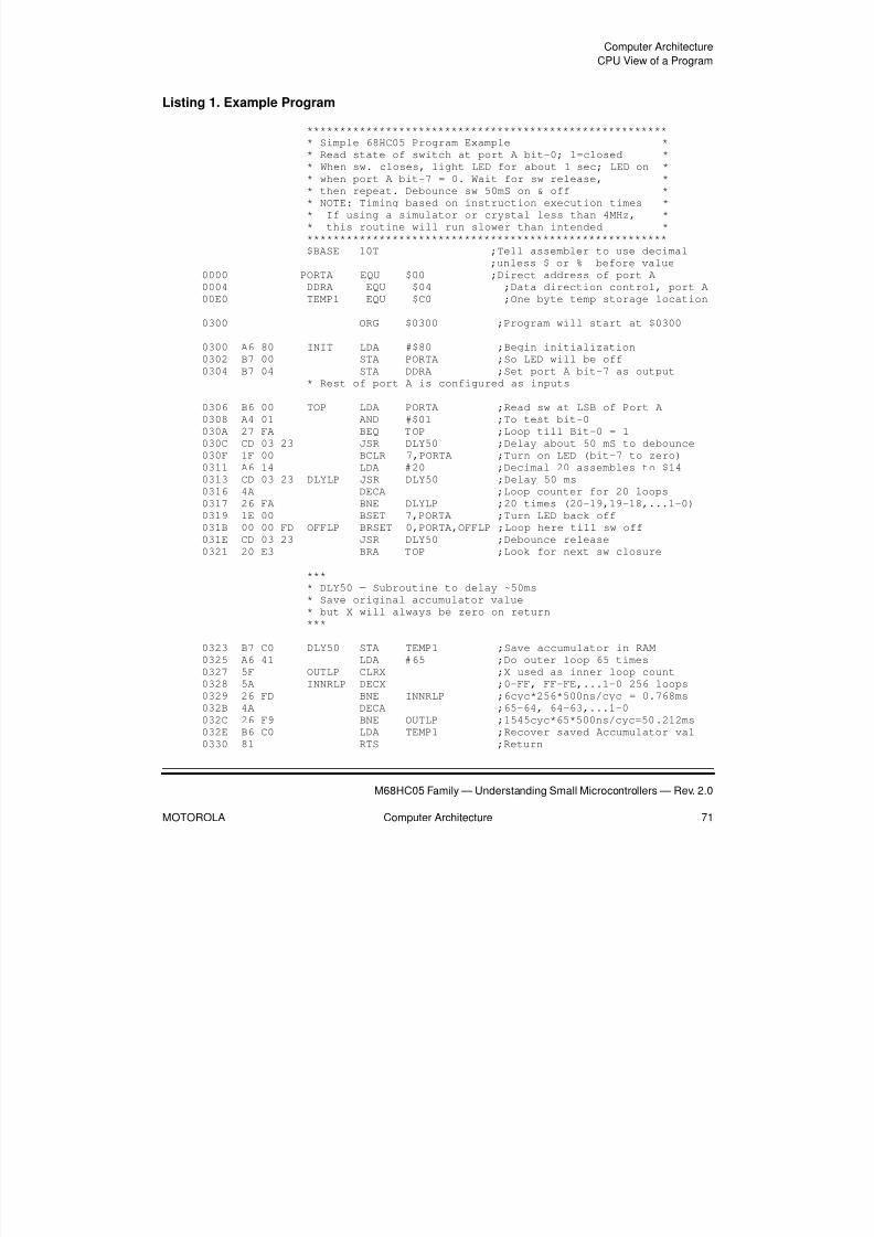
8/2/2019 122 Textbook
http://slidepdf.com/reader/full/122-textbook 71/331
Computer Architecture
CPU View of a Program
M68HC05 Family — Understanding Small Microcontrollers — Rev. 2.0
MOTOROLA Computer Architecture 71
Listing 1. Example Program
*******************************************************
* Simple 68HC05 Program Example *
* Read state of switch at port A bit-0; 1=closed *
* When sw. closes, light LED for about 1 sec; LED on ** when port A bit-7 = 0. Wait for sw release, *
* then repeat. Debounce sw 50mS on & off *
* NOTE: Timing based on instruction execution times *
* If using a simulator or crystal less than 4MHz, *
* this routine will run slower than intended *
*******************************************************
$BASE 10T ;Tell assembler to use decimal
;unless $ or % before value
0000 PORTA EQU $00 ;Direct address of port A
0004 DDRA EQU $04 ;Data direction control, port A
00E0 TEMP1 EQU $C0 ;One byte temp storage location
0300 ORG $0300 ;Program will start at $0300
0300 A6 80 INIT LDA #$80 ;Begin initialization
0302 B7 00 STA PORTA ;So LED will be off
0304 B7 04 STA DDRA ;Set port A bit-7 as output
* Rest of port A is configured as inputs
0306 B6 00 TOP LDA PORTA ;Read sw at LSB of Port A
0308 A4 01 AND #$01 ;To test bit-0
030A 27 FA BEQ TOP ;Loop till Bit-0 = 1
030C CD 03 23 JSR DLY50 ;Delay about 50 mS to debounce
030F 1F 00 BCLR 7,PORTA ;Turn on LED (bit-7 to zero)
0311 A6 14 LDA #20 ;Decimal 20 assembles to $14
0313 CD 03 23 DLYLP JSR DLY50 ;Delay 50 ms
0316 4A DECA ;Loop counter for 20 loops
0317 26 FA BNE DLYLP ;20 times (20-19,19-18,...1-0)0319 1E 00 BSET 7,PORTA ;Turn LED back off
031B 00 00 FD OFFLP BRSET 0,PORTA,OFFLP ;Loop here till sw off
031E CD 03 23 JSR DLY50 ;Debounce release
0321 20 E3 BRA TOP ;Look for next sw closure
***
* DLY50 — Subroutine to delay ~50ms
* Save original accumulator value
* but X will always be zero on return
***
0323 B7 C0 DLY50 STA TEMP1 ;Save accumulator in RAM
0325 A6 41 LDA #65 ;Do outer loop 65 times
0327 5F OUTLP CLRX ;X used as inner loop count
0328 5A INNRLP DECX ;0-FF, FF-FE,...1-0 256 loops
0329 26 FD BNE INNRLP ;6cyc*256*500ns/cyc = 0.768ms
032B 4A DECA ;65-64, 64-63,...1-0
032C 26 F9 BNE OUTLP ;1545cyc*65*500ns/cyc=50.212ms
032E B6 C0 LDA TEMP1 ;Recover saved Accumulator val
0330 81 RTS ;Return
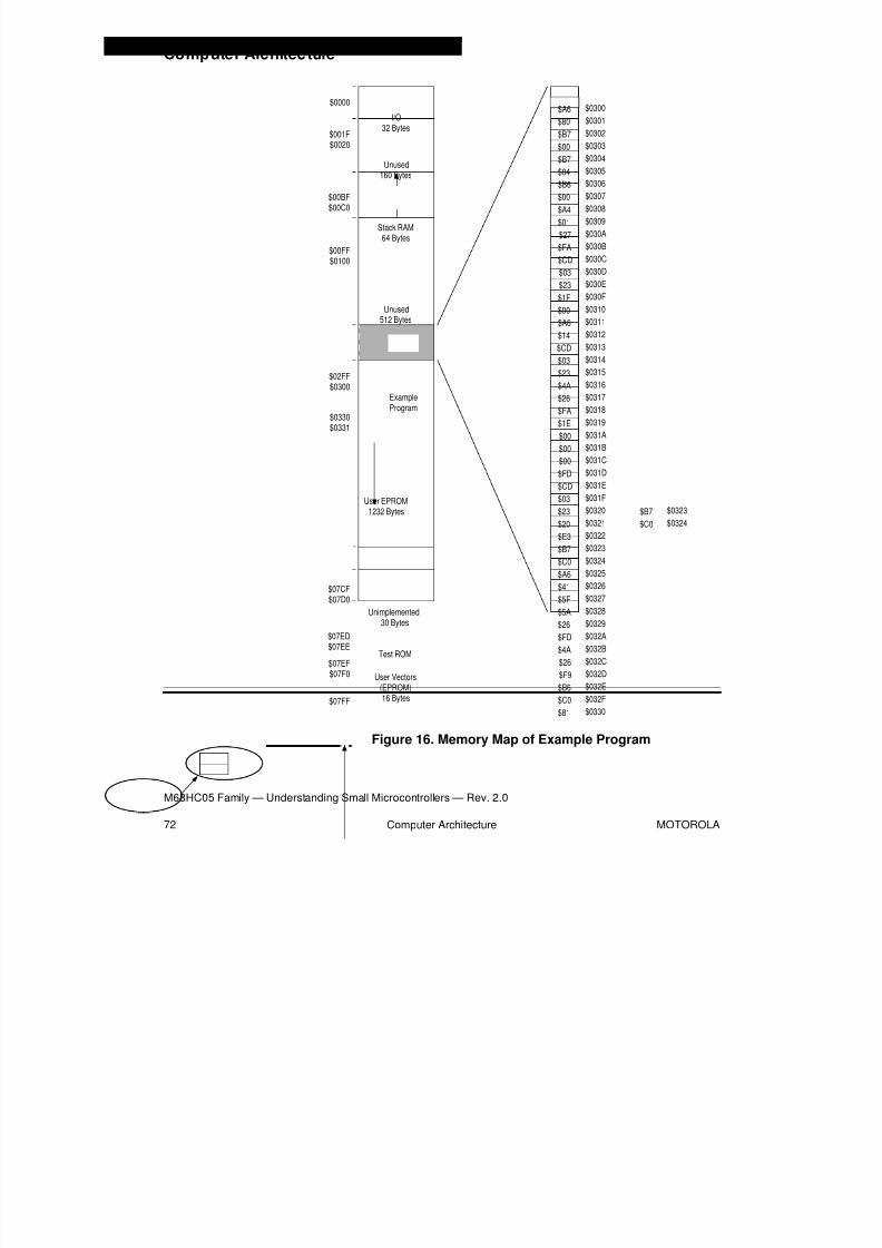
8/2/2019 122 Textbook
http://slidepdf.com/reader/full/122-textbook 72/331
Computer Architecture
M68HC05 Family — Understanding Small Microcontrollers — Rev. 2.0
72 Computer Architecture MOTOROLA
Figure 16. Memory Map of Example Program
$0000
$001F$0020
$00BF$00C0
$00FF$0100
$02FF$0300
$07ED$07EE
$07FF
I/O32 Bytes
Unused160 Bytes
Unused512 Bytes
User EPROM1232 Bytes
Stack RAM64 Bytes
$0301
$0302
$0303
$0304
$0305
$0306
$0307
$0308
$0309
$030A
$030B
$030C
$030D
$030E
$030F
$0310
$0311
$0312$0313
$0314
$0315
$0316
$0317
$0318
$0319
$031A
$031B
$031C
$031D
$031E
$031F
Test ROM
User Vectors(EPROM)16 Bytes
$07EF
$07F0
$0300
$80
$B7
$00
$B7
$04
$B6
$00
$A4
$01
$27
$FA
$CD
$03
$23
$1F
$00
$A6
$14$CD
$03
$23
$4A
$26
$FA
$1E
$00
$00
$00
$FD
$CD
$03
$A6
$0320
$0321
$0322
$0323
$0324
$0325
$0326
$0327
$0328
$0329
$032A
$032B
$032C
$032D$032E
$032F
$23
$20
$E3
$B7
$C0
$A6
$41
$5F
$5A
$26
$FD
$4A
$26
$F9$B6
$C0
$0330$81
ExampleProgram
$0330$0331
$0323
$0324
$B7
$C0
Unimplemented30 Bytes
$07CF$07D0

8/2/2019 122 Textbook
http://slidepdf.com/reader/full/122-textbook 73/331
Computer Architecture
CPU Operation
M68HC05 Family — Understanding Small Microcontrollers — Rev. 2.0
MOTOROLA Computer Architecture 73
Carefully study the program listing in Listing 1. Example Program and
the memory map of Figure 16. Find the first instruction of the DLY50
subroutine in the example program and then find the same two bytes in
Figure 16.
You should have found this line from near the bottom of
Listing 1. Example Program.
0323 B7 C0 DLY50 STA TEMP1 ;Save accumulator in RAM
The highlighted section of memory at the right side of Figure 16 is the
area you should have identified.
CPU Operation
This section first discusses the detailed operation of CPU instructions
and then explains how the CPU executes an example program. The
detailed descriptions of typical CPU instructions are intended to make
you think like a CPU. We will then go through an example program using
a teaching technique called “playing computer” in which you pretend you
are the CPU interpreting and executing the instructions in a program.
Detailed
Operation of CPU
Instructions
Before seeing how the CPU executes programs, it would help to know
(in detail) how the CPU breaks down instructions into fundamental
operations and performs these tiny steps to accomplish a desired
instruction. As we will see, many small steps execute quickly and
accurately within each instruction, but none of the small steps is too
complicated.
The logic circuitry inside the CPU would seem straightforward to a
design engineer accustomed to working with TTL (transistor-transistor
logic) logic or even relay logic. What sets the MCU and its CPU apart
from these other forms of digital logic is the packing density. Very large
scale integration (VLSI) techniques have made it possible to fit the
equivalent of thousands of TTL integrated circuits on a single silicon die.
By arranging these logic gates to form a CPU, you can get a
general-purpose instruction executor capable of acting as a universal

8/2/2019 122 Textbook
http://slidepdf.com/reader/full/122-textbook 74/331
Computer Architecture
M68HC05 Family — Understanding Small Microcontrollers — Rev. 2.0
74 Computer Architecture MOTOROLA
black box . By placing different combinations of instructions in the
device, it can perform virtually any definable function.
A typical instruction takes two to five cycles of the internal processor
clock. Although it is not normally important to know exactly whathappens during each of these execution cycles, it will help to go through
a few instructions in detail to understand how the CPU works internally.
Store
Accumulator
(Direc t Ad dressing
Mode)
Look up the STA instruction in Instruction Set Details. In the table at
the bottom of the page, we see that $B7 is the direct (DIR) addressing
mode version of the store accumulator instruction. We also see that the
instruction requires two bytes, one to specify the opcode ($B7) and the
second to specify the direct address where the accumulator will be
stored. (The two bytes are shown as B7 dd in the machine code columnof the table.)
We will discuss the addressing modes in more detail in another chapter,
but the following brief description will help in understanding howthe CPU
executes this instruction. In direct addressing modes, the CPU assumes
the address is in the range of $0000 through $00FF; thus, there is no
need to include the upper byte of the address of the operand in the
instruction (since it is always $00).
The table at the bottom of the STA page shows that the direct
addressing version of the STA instruction takes four CPU cycles to
execute. During the first cycle, the CPU puts the value from the program
counter on the internal address bus and reads the opcode $B7, which
identifies the instruction as the direct addressing version of the STA
instruction and advances the PC to the next memory location.
During the second cycle, the CPU places the value from the PC on the
internal address bus and reads the low-order byte of the direct address
($00 for example). The CPU uses the third cycle of this STA instruction
to internally construct the full address where the accumulator is to be
stored and advances the PC so it points to the next address in memory
(the address of the opcode of the next instruction).
In this example, the CPU appends the assumed value $00 (because of
direct addressing mode) to the $00 that was read during the second
cycle of the instruction to arrive at the complete address $0000. During
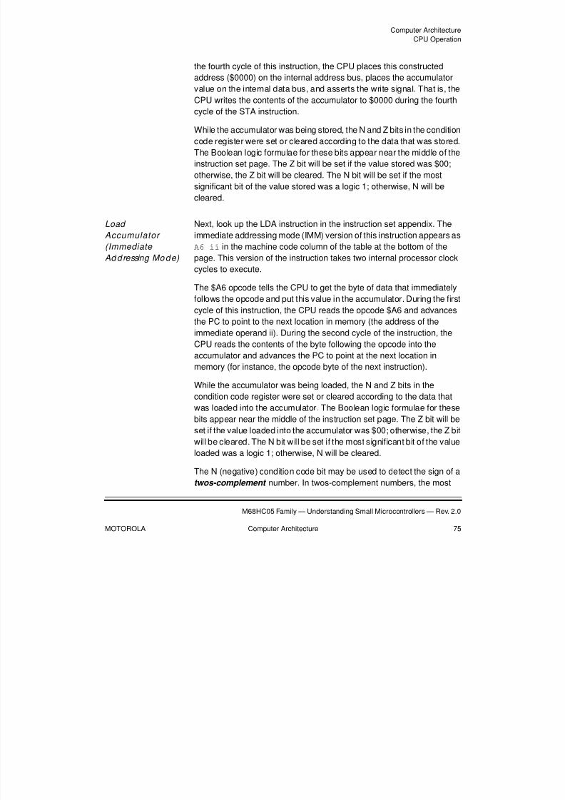
8/2/2019 122 Textbook
http://slidepdf.com/reader/full/122-textbook 75/331
Computer Architecture
CPU Operation
M68HC05 Family — Understanding Small Microcontrollers — Rev. 2.0
MOTOROLA Computer Architecture 75
the fourth cycle of this instruction, the CPU places this constructed
address ($0000) on the internal address bus, places the accumulator
value on the internal data bus, and asserts the write signal. That is, the
CPU writes the contents of the accumulator to $0000 during the fourth
cycle of the STA instruction.
While the accumulator was being stored, the N and Z bits in the condition
code register were set or cleared according to the data that was stored.
The Boolean logic formulae for these bits appear near the middle of the
instruction set page. The Z bit will be set if the value stored was $00;
otherwise, the Z bit will be cleared. The N bit will be set if the most
significant bit of the value stored was a logic 1; otherwise, N will be
cleared.
Load
Accumulator
(Immediate
Ad dressing Mo de)
Next, look up the LDA instruction in the instruction set appendix. The
immediate addressing mode (IMM) version of this instruction appears as
A6 ii in the machine code column of the table at the bottom of the
page. This version of the instruction takes two internal processor clock
cycles to execute.
The $A6 opcode tells the CPU to get the byte of data that immediately
follows the opcode and put this value in the accumulator. During the first
cycle of this instruction, the CPU reads the opcode $A6 and advances
the PC to point to the next location in memory (the address of theimmediate operand ii). During the second cycle of the instruction, the
CPU reads the contents of the byte following the opcode into the
accumulator and advances the PC to point at the next location in
memory (for instance, the opcode byte of the next instruction).
While the accumulator was being loaded, the N and Z bits in the
condition code register were set or cleared according to the data that
was loaded into the accumulator. The Boolean logic formulae for these
bits appear near the middle of the instruction set page. The Z bit will be
set if the value loaded into the accumulator was $00; otherwise, the Z bitwill be cleared. The N bit will be set if the most significant bit of the value
loaded was a logic 1; otherwise, N will be cleared.
The N (negative) condition code bit may be used to detect the sign of a
twos-complement number. In twos-complement numbers, the most

8/2/2019 122 Textbook
http://slidepdf.com/reader/full/122-textbook 76/331
Computer Architecture
M68HC05 Family — Understanding Small Microcontrollers — Rev. 2.0
76 Computer Architecture MOTOROLA
significant bit is used as a sign bit, 1 indicates a negative value, and 0
indicates a positive value. The N bit may also be used as a simple
indication of the state of the most significant bit of a binary value.
Conditional
Branch
Branch instructions allow the CPU to select one of two program flow
paths, depending upon the state of a particular bit in memory or various
condition code bits. If the condition checked by the branch instruction is
true, program flow skips to a specified location in memory. If the
condition checked by the branch is not true, the CPU continues to the
instruction following the branch instruction. Decision blocks in a
flowchart correspond to conditional branch instructions in the program.
Most branch instructions contain two bytes, one for the opcode and one
for a relative offset byte. Branch on bit clear (BRCLR) and branch on bitset (BRSET) instructions require three bytes: the opcode, a 1-byte direct
address (to specify the memory location to be tested), and the relative
offset byte.
The relative offset byte is interpreted by the CPU as a twos-complement
signed value. If the branch condition checked is true, this signed offset
is added to the PC, and the CPU reads its next instruction from this
calculated new address. If the branch condition is not true, the CPU just
continues to the next instruction after the branch instruction.
Sub routine Ca lls
and Returns
The jump-to-subroutine (JSR) and branch-to-subroutine (BSR)
instructions automate the process of leaving the normal linear flow of a
program to go off and execute a set of instructions and then return to
where the normal flow left off. The set of instructions outside the normal
program flow is called a subroutine. A JSR or BSR instruction is used to
go from the running program to the subroutine. A return-from-subroutine
(RTS) instruction is used, at the completion of the subroutine, to return
to the program from which the subroutine was called.
The Listing 2. Subroutine Call Example shows lines of an assemblerlisting that will be used to demonstrate how the CPU executes a
subroutine call. Assume that the stack pointer (SP) points to address
$00FF when the CPU encounters the JSR instruction at location $0302.
Assembler listings are described in greater detail in the chapter entitled
Programming.

8/2/2019 122 Textbook
http://slidepdf.com/reader/full/122-textbook 77/331
Computer Architecture
CPU Operation
M68HC05 Family — Understanding Small Microcontrollers — Rev. 2.0
MOTOROLA Computer Architecture 77
Listing 2. Subroutine Call Example
“ “ “ “ “
0300 A6 02 TOP LDA #$02 ;Load an immediate value
0302 CD 04 00 JSR SUBBY ;Go do a subroutine
0305 B7 E0 STA $E0 ;Store accumulator to RAM0307 “ “ “ “
“ “ “ “ “
“ “ “ “ “
0400 4A SUBBY DECA ;Decrement accumulator
0401 26 FD BNE SUBBY ;Loop till accumulator=0
0403 81 RTS ;Return to main program
Refer to Figure 17 during the following discussion. We begin the
explanation with the CPU executing the instruction LDA #$02 at address
$0300. The left side of the figure shows the normal program flow
composed of TOP LDA #$02, JSR SUBBY, and STA $E0 (in that order)
in consecutive memory locations. The right half of the figure shows
subroutine instructions SUBBY DECA, BNE SUBBY, and RTS.
Figure 17. Subroutine Call Sequence
The CPU clock cycle numbers (in square brackets) are used as
references in the following explanation of Figure 17.
$00
$A6$0300 $4A $0400
$02$0301
$CD$0302
$04$0303
$0304
$B7$0305
$E0$0306
$26 $0401
$FD $0402
$81 $0403
SUBBY DECA
BNE SUBBY
RTS
TOP LDA #$02
JSR SUBBY
STA $E0
[1]
[2]
[3]
[4]
[5]
[27]
[28]
[9]
[10]
[11]
[12]
[13]
[22]
[29]
[30]
[14]
[21]
[23]
[24]
[25]
[26]
[15]
[16]
[17]
[18]
[19]
[20]
[6]
[7]
[8]
START

8/2/2019 122 Textbook
http://slidepdf.com/reader/full/122-textbook 78/331
Computer Architecture
M68HC05 Family — Understanding Small Microcontrollers — Rev. 2.0
78 Computer Architecture MOTOROLA
[1] CPU reads $A6 opcode from location $0300 (LDA
immediate).
[2] CPU reads immediate data $02 from location $0301 into the
accumulator.
[3] CPU reads $CD opcode from location $0302 (JSR
extended).
[4] CPU reads high-order extended address $04 from $0303.
[5] CPU reads low-order extended address $00 from $0304.
[6] CPU builds full address of subroutine ($0400).
[7] CPU writes $05 to $00FF and decrements SP to $00FE.
Another way to say this is “push low-order half of return
address on stack.”
[8] CPU writes $03 to $00FE and decrements SP to $00FD.
Another way to say this is “push high-order half of return
address on stack.” The returnaddress that was saved on the
stack is $0305, which is the address of the instruction that
follows the JSR instruction.
[9] CPU reads $4A opcode from location $0400. This is the first
instruction of the called subroutine.
[10] The CPU uses its ALU to subtract one from the value in the
accumulator.
[11] The ALU result (A – 1) is written back to the accumulator.
[12] CPU reads BNE opcode ($26) from location $0401.
[13] CPU reads relative offset ($FD) from $0402.
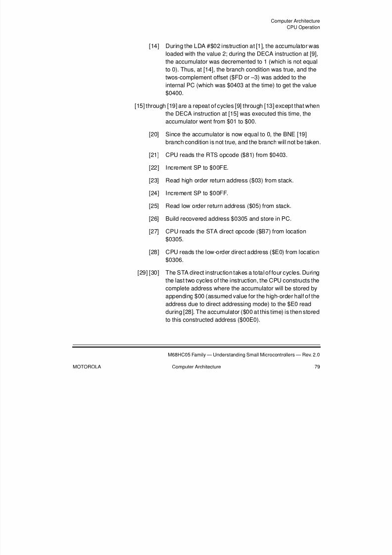
8/2/2019 122 Textbook
http://slidepdf.com/reader/full/122-textbook 79/331
Computer Architecture
CPU Operation
M68HC05 Family — Understanding Small Microcontrollers — Rev. 2.0
MOTOROLA Computer Architecture 79
[14] During the LDA #$02 instruction at [1], the accumulator was
loaded with the value 2; during the DECA instruction at [9],
the accumulator was decremented to 1 (which is not equal
to 0). Thus, at [14], the branch condition was true, and the
twos-complement offset ($FD or –3) was added to the
internal PC (which was $0403 at the time) to get the value
$0400.
[15] through [19] are a repeat of cycles [9] through [13] except that when
the DECA instruction at [15] was executed this time, the
accumulator went from $01 to $00.
[20] Since the accumulator is now equal to 0, the BNE [19]
branch condition is not true, and the branch will not be taken.
[21] CPU reads the RTS opcode ($81) from $0403.
[22] Increment SP to $00FE.
[23] Read high order return address ($03) from stack.
[24] Increment SP to $00FF.
[25] Read low order return address ($05) from stack.
[26] Build recovered address $0305 and store in PC.
[27] CPU reads the STA direct opcode ($B7) from location
$0305.
[28] CPU reads the low-order direct address ($E0) from location
$0306.
[29] [30] The STA direct instruction takes a total of four cycles. During
the last two cycles of the instruction, the CPU constructs the
complete address where the accumulator will be stored by
appending $00 (assumed value for the high-order half of the
address due to direct addressing mode) to the $E0 read
during [28]. The accumulator ($00 at this time) is then stored
to this constructed address ($00E0).

8/2/2019 122 Textbook
http://slidepdf.com/reader/full/122-textbook 80/331
Computer Architecture
M68HC05 Family — Understanding Small Microcontrollers — Rev. 2.0
80 Computer Architecture MOTOROLA
Playing Computer
Playing computer is a learning exercise where you pretend to be a
CPU that is executing a program. Programmers often mentally checkprograms by playing computer as they read through a software routine.
While playing computer, it is not necessary to break instructions down to
individual processor cycles. Instead, an instruction is treated as a single
complete operation rather than several detailed steps.
The following paragraphs demonstrate the process of playing computer
by going through the subroutine-call exercise of Figure 17. The
playing-computer approach to analyzing this sequence is much less
detailed than the cycle-by-cycle analysis done earlier, but it
accomplishes the same basic goal (for instance, it shows what happensas the CPU executes the sequence). After studying the chapter on
programming, you should attempt the same thing with a larger program.
You begin the process by preparing a worksheet like that shown in
Figure 18. This sheet includes the mnemonic program and the machine
code that it assembles to. (You could alternately choose to use a listing
positioned next to the worksheet.) The worksheet also includes the CPU
register names across the top of the sheet. There is ample room below
to write new values as the registers change in the course of the program.
On this worksheet, there is an area for keeping track of the stack. After
you become comfortable with how the stack works, you would probably
leave this section off, but it will be instructive to leave it here for now.
As a value is saved on the stack, you will cross out any prior value and
write the new value to its right in a horizontal row. You must also update
(decrement) the SP value. Cross out any prior value and write the new
value beneath it under the SP heading at the top of the worksheet. As a
value is recovered from the stack, you would update (increment) the
value of SP by crossing out the old value and writing the new valuebelow it. You would then read the value from the location now pointed to
by the SP and put it wherever it belongs in the CPU (for instance, in the
upper or lower half of the PC).

8/2/2019 122 Textbook
http://slidepdf.com/reader/full/122-textbook 81/331
Computer Architecture
Playing Computer
M68HC05 Family — Understanding Small Microcontrollers — Rev. 2.0
MOTOROLA Computer Architecture 81
Figure 18. Worksheet for Playing Computer
0300 A6 02 TOP LDA #$02 ;Load an immediate value
0302 CD 04 00 JSR SUBBY ;Go do a subroutine
0305 B7 02 STA $E0 ;Store accumulator to RAM
" " " " "
" " " " "
" " " " "
0400 4A SUBBYDECA ;Decrement accumulator
0401 26 FD BNE SUBBY ;Loop till accumulator = 0
0403 81 RTS ;Return to main program
$00FC$00FD$00FE$00FF
AccumulatorCond. Codes
1 1 1 H I N Z CProgramCounterStack Pointer
IndexRegister
L I S T I N
G o f P R
O G RA
M
t o b e E
XA M I N E
D

8/2/2019 122 Textbook
http://slidepdf.com/reader/full/122-textbook 82/331
Computer Architecture
M68HC05 Family — Understanding Small Microcontrollers — Rev. 2.0
82 Computer Architecture MOTOROLA
Figure 19 shows how the worksheet will look after working through the
whole JSR sequence. Follow the numbers in square brackets as the
process is explained. During the process, many values were written and
later crossed out; a line has been drawn from the square bracket to
either the value or the crossed-out mark to show which item the
reference number applies to.
Figure 19. Completed Worksheet
0300 A6 02 TOP LDA #$02 ;Load an immediate value
0302 CD 04 00 JSR SUBBY ;Go do a subroutine
0305 B7 02 STA $E0 ;Store accumulator to RAM
" " " " "
" " " " "
" " " " "
0400 4A SUBBYDECA ;Decrement accumulator
0401 26 FD BNE SUBBY ;Loop till accumulator = 0
0403 81 RTS ;Return to main program
$00FC
$00FD
$00FE$00FF
AccumulatorCond. Codes
1 1 1 H I N Z CProgramCounterStack Pointer
IndexRegister
1 1 1 ? ? 0 0 ?
1 1 1 ? ? 0 1 ?
$02
$01
$00
$0300
$0302
$0400
$0401
$0400
$0401
$0403
$0305
$00FF
$00FE
$00FD
$00FE
$00FF
$03 $05
$00E0 – RAM $00
[11]
[14]
[7]
[9]
[18]
[19]
[4]
[10]
[12]
[13]
[16]
[17]
[20]
[1][2] [3] [5] [15]
[21]
[6]
[8]

8/2/2019 122 Textbook
http://slidepdf.com/reader/full/122-textbook 83/331
Computer Architecture
Playing Computer
M68HC05 Family — Understanding Small Microcontrollers — Rev. 2.0
MOTOROLA Computer Architecture 83
Beginning the sequence:
• The PC should be pointing to $0300 [1] and the SP should be
pointing to $00FF [2] (due to an earlier assumption).
• The CPU reads and executes the LDA #$02 instruction (load
accumulator with the immediate value $02).
• Thus, you write $02 in the accumulator column [3] and replace the
PC value [4] with $0302, which is the address of the next
instruction.
• The load accumulator instruction affects the N and Z bits in the
CCR. Since the value loaded was $02, the Z bit would be cleared,
and the N bit would be cleared [5]. This information can be found
in the Load Accumulator from Memory LDA section of the
chapter Instruction Set Details .
• Since the other bits in the CCR are not affected by the LDA
instruction, we have no way of knowing what they should be at this
time, so for now we put question marks in the unknown positions
[5].
Next:
• The CPU reads the JSR SUBBY instruction. Temporarily,
remember the value $0305, which is the address where the CPUshould come back to, after executing the called subroutine. The
CPU saves the low-order half of the return address on the stack.
• Thus, you write $05 [6] at the location pointed to by the SP
($00FF) and decrement the SP [7] to $00FE.
• The CPU then saves the high-order half of the return address on
the stack.
• You write $03 [8] to $00FE and again decrement the SP [9], this
time to $00FD.
• To finish the JSR instruction, you load the PC with $0400 [10],
which is the address of the called subroutine.
• The CPU fetches the next instruction. Since the PC is $0400, the
CPU executes the DECA instruction, the first instruction in the
subroutine.

8/2/2019 122 Textbook
http://slidepdf.com/reader/full/122-textbook 84/331
Computer Architecture
M68HC05 Family — Understanding Small Microcontrollers — Rev. 2.0
84 Computer Architecture MOTOROLA
• You cross out the $02 in the accumulator column and write the
new value $01 [11].
• You also change the PC to $0401 [12].
• Because the DECA instruction changed the accumulator from $02to $01 (which is not zero or negative), the Z bit and N bit remain
clear. Since N and Z were already cleared at [5], you can leave
them alone on the worksheet.
• The CPU now executes the BNE SUBBY instruction. Since the Z
bit is clear, the branch condition is met, and the CPU will take the
branch. Cross out the $0401 under PC and write $0400 [13].
• The CPU again executes the DECA instruction. The accumulator
is now changed from $01 to $00 [14] (which is 0 and not negative);
thus, the Z bit is set, and the N bit remains clear [15].
• The PC advances to the next instruction [16].
• The CPU now executes the BNE SUBBY instruction, but this time
the branch condition is not true (Z is set now), so the branch will
not be taken. The CPU simply falls to the next instruction (the RTS
at $0403).
• Update the PC to $0403 [17].
• The RTS instruction causes the CPU to recover the previously
stacked PC. Pull the high-order half of the PC from the stack byincrementing the SP to $00FE [18] and by reading $03 from
location $00FE.
• Next, pull the low-order half of the address from the stack by
incrementing SP to $00FF [19] and by reading $05 from $00FF.
The address recovered from the stack replaces the value in the
PC [20].
• The CPU now reads the STA $E0 instruction from location $0305.
Program flow has returned to the main program sequence where
it left off when the subroutine was called.
• The STA (direct addressing mode) instruction writes the
accumulator value to the direct address $E0 ($00E0), which is in
the RAM of the MC68HC705J1A. We can see from the worksheet
that the current value in the accumulator is $00; therefore, all eight
8/2/2019 122 Textbook
http://slidepdf.com/reader/full/122-textbook 85/331
Computer Architecture
Playing Computer
M68HC05 Family — Understanding Small Microcontrollers — Rev. 2.0
MOTOROLA Computer Architecture 85
bits of this RAM location will be cleared. Since the original
worksheet did not have a place marked for recording this value in
RAM, you would make a place and write $00 there [21].
For a larger program, the worksheet would have many more crossed outvalues by the time you are done. Playing computer on a worksheet like
this is a good learning exercise, but, as a programmer gains experience,
the process would be simplified. In the programming chapter, we will see
a development tool called a simulator that automates the playing
computer process. The simulator is a computer program that runs on a
personal computer. The current contents of registers and memory
locations are displayed on the terminal display of the personal computer.
One of the first simplifications you could make to a manual worksheet
would be to quit keeping track of the PC because you learn to trust theCPU to take care of this for you. Another simplification is to stop keeping
track of the condition codes. When a branch instruction that depends on
a condition code bit is encountered, you can mentally work backward to
decide whether or not the branch should be taken.
Next, the storage of values on the stack would be skipped, although it is
still a good idea to keep track of the SP value itself. It is fairly common
to have programming errors resulting from incorrect values in the SP. A
fundamental operating principle of the stack is that over a period of time,
the same number of items must be removed from the stack as were puton the stack. Just as left parentheses must be matched with right
parentheses in a mathematical formula, JSRs and BSRs must be
matched one for one to subsequent RTSs in a program. Errors that
cause this rule to be broken will appear as erroneous SP values while
playing computer.
Even an experienced programmer will play computer occasionally to
solve some difficult problem. The procedure the experienced
programmer would use is much less formal than what was explained
here, but it still amounts to placing yourself in the role of the CPU andworking out what happens as the program is executed.

8/2/2019 122 Textbook
http://slidepdf.com/reader/full/122-textbook 86/331
Computer Architecture
M68HC05 Family — Understanding Small Microcontrollers — Rev. 2.0
86 Computer Architecture MOTOROLA
Resets
Reset is used to force the MCU system to a known starting place
(address). Peripheral systems and many control and status bits are alsoforced to a known state as a result of reset.
These internal actions occur as the result of any MCU reset:
1. All data direction registers cleared to 0 (input)
2. Stack pointer forced to $00FF
3. I bit in the CCR set to 1 to inhibit maskable interrupts
4. External interrupt latch cleared
5. STOP latch cleared
6. WAIT latch cleared
As the computer system leaves reset, the program counter is loaded
from the two highest memory locations ($07FE and $07FF in an
MC68HC705J1A). The value from $07FE is loaded into the high order
byte of the PC and the value from $07FF is loaded into the low order byte
of the PC. This is called “fetching the reset vector .” At this point, the
CPU begins to fetch and execute instructions, beginning at the address
that was stored in the reset vector.
Any of these conditions can cause the MC68HC705J1A MCU to reset:
1. External, active-low input signal on the RESET pin
2. Internal power-on reset (POR)
3. Internal computer operating properly (COP) watchdog timed out
4. An attempt to execute an instruction from an illegal address
RESET Pin An external switch or circuit can be connected to this pin to allow a
manual system reset.
Power-On Reset The power-on reset occurs when a positive transition is detected on
VDD. The power-on reset is used strictly for power turn-on conditions

8/2/2019 122 Textbook
http://slidepdf.com/reader/full/122-textbook 87/331
Computer Architecture
Resets
M68HC05 Family — Understanding Small Microcontrollers — Rev. 2.0
MOTOROLA Computer Architecture 87
and should not be used to detect any drops in the power supply voltage.
A low-voltage inhibit (LVI) circuit should be used to detect loss of power.
The power-on circuitry provides for a 4064-cycle delay from the time that
the oscillator becomes active. If the external RESET pin is low at the endof the 4064-cycle delay timeout, the processor remains in the reset
condition until RESET goes high.
Watchdog Timer
Reset
The computer operating properly (COP) watchdog timer system is
intended to detect software errors. When the COP is being used,
software is responsible for keeping a free-running watchdog timer from
timing out. If the watchdog timer times out, it is an indication that
software is no longer being executed in the intended sequence; thus, a
system reset is initiated.
A control bit in the non-volatile mask option control register can be used
to enable or disable the COP reset. If the COP is enabled, the operating
program must periodically write a 0 to the COPC bit in the COPR control
register. Refer to the MC68HC705J1A Technical Data (Motorola order
number MC68HC705J1A/D) for information about the COP timeout rate.
Some members of the M68HC05 Family have different COP watchdog
timer systems.
Illegal Address
Reset
If a program is written incorrectly, it is possible that the CPU will attempt
to jump or branch to an address that has no memory. If this happened,
the CPU would continue to read data (though it would be unpredictable
values) and attempt to act on it as if it were a program. These nonsense
instructions could cause the CPU to write unexpected data to
unexpected memory or register addresses. This situation is called
program runaway.
To guard against this runaway condition, there is an illegal address
detect circuit in the MC68HC705J1A. If the CPU attempts to fetch aninstruction from an address that is not in the EPROM ($0300–$07CF,
$07F0–$07FF), internal test ROM ($07EE–$07EF), or RAM
($00C0–$00FF), a reset is generated to force the program to start over.

8/2/2019 122 Textbook
http://slidepdf.com/reader/full/122-textbook 88/331
Computer Architecture
M68HC05 Family — Understanding Small Microcontrollers — Rev. 2.0
88 Computer Architecture MOTOROLA
Interrupts
It is sometimes useful to interrupt normal processing to respond to some
unusual event. For instance, the MC68HC705J1A may be interrupted byany of these sources:
1. A logic 0 applied to the external interrupt IRQ pin
2. A logic 1 applied to any of the PA3–PA0 pins, provided the portinterrupt function is enabled
3. A timer overflow (TOF) or real-time interrupt (RTIF) request fromthe on-chip multifunctional timer system, if enabled
4. The software interrupt (SWI) instruction
If an interrupt comes while the CPU is executing an instruction, theinstruction is completed before the CPU responds to the interrupt.
Interrupts can be inhibited by setting the I bit in the condition code
register (CCR) or by clearing individual interrupt enable control bits for
each interrupt source. Reset forces the I bit to 1 and clears all local
interrupt enable bits to prevent interrupts during the initialization
procedure. When the I bit is 1, no interrupts (except the SWI instruction)
are recognized. However, interrupt sources may still register a request
that will be honored at some later time when the I bit is cleared.
Figure 20 shows how interrupts fit into the normal flow of CPU
instructions. Interrupts cause the processor registers to be saved on the
stack and the interrupt mask (I bit) to be set, to prevent additional
interrupts until the present interrupt is finished. The appropriate interrupt
vector then points to the starting address of the interrupt service routine
(Table 10). Upon completion of the interrupt service routine, an RTI
instruction (which is normally the last instruction of an interrupt service
routine) causes the register contents to be recovered from the stack.
Since the program counter is loaded with the value that was previously
saved on the stack, processing continues from where it left off before the

8/2/2019 122 Textbook
http://slidepdf.com/reader/full/122-textbook 89/331
Computer Architecture
Interrupts
M68HC05 Family — Understanding Small Microcontrollers — Rev. 2.0
MOTOROLA Computer Architecture 89
interrupt. Figure 21 shows that registers are restored from the stack in
the opposite order they were saved.
Table 10. Vector Addresses for Resets and Interrupts
on the MC68HC705J1A
Reset or Interrupt Source Vector Address
On-Chip Timer $07F8, $07F9
IRQ or Port A Pins $07FA, $07FB
SWI Instruction $07FC, $07FD
Reset (POR, LVI, Pin, COP, or Illegal Address) $07FE, $07FF

8/2/2019 122 Textbook
http://slidepdf.com/reader/full/122-textbook 90/331
Computer Architecture
M68HC05 Family — Understanding Small Microcontrollers — Rev. 2.0
90 Computer Architecture MOTOROLA
Figure 20. Hardware Interrupt Flowchart
FROM
RESET
YES
NO
STACKPC, X, A, CCR
YES
NO
YES
NO
CLEAR IRQREQUEST LATCH
SET I BIT
IN CCR
LOAD PC FROM VECTOR:SWI: $07FC, $07FD
IRQ OR PORT A: $07FA, $07FB
TIMER: $07F8, $07F9
YES
NO
RTI INSTRUCTION ?RESTORE REGISTERS
FROM STACKCCR, A, X, PC
FETCH NEXT
INSTRUCTION
EXECUTE
INSTRUCTION
I BIT IN CCR SET ?
EXTERNAL INTERRUPT ?
(IRQ OR PORT A)
TIMER INTERRUPT ?
YES
NO
SWI INSTRUCTION ?

8/2/2019 122 Textbook
http://slidepdf.com/reader/full/122-textbook 91/331
Computer Architecture
Interrupts
M68HC05 Family — Understanding Small Microcontrollers — Rev. 2.0
MOTOROLA Computer Architecture 91
Figure 21. Interrupt Stacking Order
External Interrupts External interrupts come from the IRQ pin or from bits 3–0 of port A if port
A is configured for port interrupts. In the MC68HC705J1A MCU, the IRQ
pin sensitivity is software programmable.
In the MC68HC705J1A MCU, two choices of external interrupts areavailable:
• Edge-sensitive triggering only
• Negative edge- and level-sensitive triggering
The MC68HC705J1A MCU uses a bit in an option register at location
$07F1 to configure the IRQ pin sensitivity. The IRQ pin is low true and
the port A interrupts are high true.
When an interrupt is recognized, the current state of the CPU is pushed
onto the stack and the I bit is set. This masks further interrupts until the
present one is serviced. The address of the external interrupt service
routine is specified by the contents of memory locations $07FA and
$07FB.
ACCUMULATOR
CONDITION CODES
INDEX REGISTER
1 1 1
PROGRAM COUNTER LOW
PC HIGH0 0 0
7 0
I N T E R R U P T
R E T U R N
TOWARD HIGHER ADDRESSES
HIGHEST STACK ADDRESS IS $00FF
TOWARD LOWER ADDRESSES
LOWEST STACK ADDRESS IS $00C0
UNSTACK
STACK
0 0
NOTE: When an interrupt occurs, CPU registers aresaved on the stack in the order PCL,PCH, X, A, CCR.On a return-from-interrupt, registers are recoveredfrom the stack in reverse order.
8/2/2019 122 Textbook
http://slidepdf.com/reader/full/122-textbook 92/331
Computer Architecture
M68HC05 Family — Understanding Small Microcontrollers — Rev. 2.0
92 Computer Architecture MOTOROLA
On-Chip
Peripheral
Interrupts
Microcontrollers often include on-chip peripheral systems that can
generate interrupts to the CPU. The timer system in the
MC68HC705J1A is an example of such a peripheral. On-chip peripheral
interrupts work just like external interrupts except that there are normally
separate interrupt vectors for each on-chip peripheral system.
Software Interrupt
(SWI)
The software interrupt is an executable instruction. The action of the SWI
instruction is similar to the hardware interrupts. An SWI is executed
regardless of the state of the interrupt mask (I bit) in the condition code
register. The interrupt service routine address is specified by the
contents of memory location $07FC and $07FD in an MC68HC705J1A.
Interrupt Latency Although we think of interrupts as if they cause the CPU to stop normal
processing immediately in order to respond to the interrupt request, this
is not quite the case. There is a small delay from when an interrupt is
requested until the CPU can actually respond. First, the CPU must finish
any instruction that happens to be in progress at the time the interrupt is
requested. (The CPU would not know how to resume processing after
the interrupt was handled if it had stopped in the middle of an
instruction.) Second, the CPU must make a record of what it was doing
before it responded to the interrupt. The CPU does this by storing a copy
of the contents of all its registers, including the program counter, on thestack. After the interrupt has been serviced, the CPU recovers this
information in reverse order and normal processing resumes.
Interrupt latency is the total number of CPU cycles (time) from the initial
interrupt request until the CPU starts to execute the first instruction of the
interrupt service routine. This delay depends upon whether or not the I
interrupt mask is set to 1 when the interrupt is requested. If the I bit is
set, the delay could be indefinite and depends upon when an instruction
clears the I bit so the interrupt can be recognized by the CPU. In the
normal case, where the I bit is clear when the interrupt is requested, thelatency will consist of finishing the current instruction, saving the
registers on the stack, and loading the interrupt vector (address of the
interrupt service routine) into the program counter.
8/2/2019 122 Textbook
http://slidepdf.com/reader/full/122-textbook 93/331
Computer Architecture
Interrupts
M68HC05 Family — Understanding Small Microcontrollers — Rev. 2.0
MOTOROLA Computer Architecture 93
The longest instruction (execution time) in the M68HC05 is the multiply
(MUL) instruction, which takes 11 bus cycles. If the CPU had just started
to execute a MUL instruction when an interrupt was requested, a delay
of up to 11 cycles would be experienced before the CPU could respond.
It takes the CPU nine bus cycles to save a copy of its registers on the
stack and to fetch the interrupt vector. The total worst-case latency if I
was clear and a MUL instruction just started would be 20 cycles (11 + 9).
The I bit is set to 1 as the CPU responds to an interrupt so that (normally)
a new interrupt will not be recognized until the current one has been
handled. In a system that has more than one source of interrupts, the
execution time for the longest interrupt service routine must be
calculated in order to determine the worst-case interrupt latency for the
other interrupt sources.
Nested Interrupts In unusual cases, an interrupt service routine may take so long to
execute that the worst-case latency for other interrupts in the system is
too long. In such a case, instructions in the long interrupt service routine
could clear the I bit to zero, thus allowing a new interrupt to be
recognized before the first interrupt service routine is finished. If a new
interrupt is requested while the CPU is already servicing an interrupt, it
is called nesting. You must use great care if you allow interrupt nesting
because the stack must have enough space to hold more than one copyof the CPU registers. On small microcontrollers like the MC68HC05K1,
the stack is small and nesting of interrupts is not recommended.

8/2/2019 122 Textbook
http://slidepdf.com/reader/full/122-textbook 94/331
Computer Architecture
M68HC05 Family — Understanding Small Microcontrollers — Rev. 2.0
94 Computer Architecture MOTOROLA
Review
In the M68HC05 architecture, five CPU registers are directly connected
within the CPU and are not part of the memory map. All other informationavailable to the CPU is located in a series of 8-bit memory locations. A
memory map shows the names and types of memory at all locations
that are accessible to the CPU. The expression memory-mapped I/O
means that the CPU treats I/O and control registers exactly like any
other kind of memory. (Some computer architectures separate the I/O
registers from program memory space and use separate instructions to
access I/O locations.)
To get started in a known place, a computer must be reset . Reset forces
on-chip peripheral systems and I/O logic to known conditions and loadsthe program counter with a known starting address. The user specifies
the desired starting location by placing the upper and lower order bytes
of this address in the reset vector locations ($07FE and $07FF on the
MC68HC705J1A).
The CPU uses the stack pointer (SP) register to implement a
last-in-first-out stack in RAM memory. This stack holds return addresses
while the CPU is executing a subroutine and holds the previous contents
of all CPU registers while the CPU is executing an interrupt sequence.
By recovering this information from the stack, the CPU can resumewhere it left off before the subroutine or interrupt was started.
Computers use a high speed clock to step through each small substep
of each operation. Although each instruction takes several cycles of this
clock, it is so fast that operations seem to be instantaneous to a human.
An MC68HC705J1A can execute about 500,000 instructions per
second.
A CPU sees a program as a linear sequence of 8-bit binary numbers.
Instruction opcodes and data are mixed in this sequence but the CPUremains aligned to instruction boundaries because each opcode tells the
CPU how many operand data bytes go with each instruction opcode.
Playing computer is a learning exercise where you pretend to be a
CPU that is executing a program.

8/2/2019 122 Textbook
http://slidepdf.com/reader/full/122-textbook 95/331
Computer Architecture
Review
M68HC05 Family — Understanding Small Microcontrollers — Rev. 2.0
MOTOROLA Computer Architecture 95
Reset can be caused by internal or external conditions. A reset pin
allows an external cause to initiate a reset. A watchdog timer and an
illegal address detect system can cause reset in the event software is
not executing in the intended sequence.
Interrupts cause the CPU to temporarily stop main program processing
to respond to the interrupt. All CPU registers are saved on the stack so
the CPU can go back to where it left off in the main program as soon as
the interrupt is serviced.
Interrupts can be inhibited globally by setting the I bit in the CCR or
locally by clearing enable control bits for each interruptsource. Requests
can still be registered while interrupts are inhibited so the CPU can
respond as soon as the interrupts are re-enabled. SWI is an instruction
and cannot be inhibited.
Interrupt latency is the delay from when an interrupt is requested to
when the CPU begins executing the first instruction in the interrupt
response program. When a CPU responds to a new interrupt while it is
already processing an interrupt (which is not normally allowed), it is
called a nested interrupt .

8/2/2019 122 Textbook
http://slidepdf.com/reader/full/122-textbook 96/331
Computer Architecture
M68HC05 Family — Understanding Small Microcontrollers — Rev. 2.0
96 Computer Architecture MOTOROLA

8/2/2019 122 Textbook
http://slidepdf.com/reader/full/122-textbook 97/331
M68HC05 Family — Understanding Small Microcontrollers — Rev. 2.0
MOTOROLA M68HC05 Instruction Set 97
M68HC05 Instruction Set
Contents
Introduction . . . . . . . . . . . . . . . . . . . . . . . . . . . . . . . . . . . . . . . . . . . . .98
Central Processor Unit (CPU) . . . . . . . . . . . . . . . . . . . . . . . . . . . . . . . 98
Arithmetic/Logic Unit (ALU). . . . . . . . . . . . . . . . . . . . . . . . . . . . . . .98CPU Control . . . . . . . . . . . . . . . . . . . . . . . . . . . . . . . . . . . . . . . . . .99CPU Registers . . . . . . . . . . . . . . . . . . . . . . . . . . . . . . . . . . . . . . . .99
Accumulator . . . . . . . . . . . . . . . . . . . . . . . . . . . . . . . . . . . . . . .100Index Register. . . . . . . . . . . . . . . . . . . . . . . . . . . . . . . . . . . . . .100Condition Code Register. . . . . . . . . . . . . . . . . . . . . . . . . . . . . .100Half-Carry Bit (H) . . . . . . . . . . . . . . . . . . . . . . . . . . . . . . . . . . .101Interrupt Mask Bit (I) . . . . . . . . . . . . . . . . . . . . . . . . . . . . . . . . . 101Negative Bit (N). . . . . . . . . . . . . . . . . . . . . . . . . . . . . . . . . . . . .101Zero Bit (Z) . . . . . . . . . . . . . . . . . . . . . . . . . . . . . . . . . . . . . . . .102Carry/Borrow Bit (C) . . . . . . . . . . . . . . . . . . . . . . . . . . . . . . . . .102Program Counter . . . . . . . . . . . . . . . . . . . . . . . . . . . . . . . . . . .103Stack Pointer . . . . . . . . . . . . . . . . . . . . . . . . . . . . . . . . . . . . . .103
Addressing Modes. . . . . . . . . . . . . . . . . . . . . . . . . . . . . . . . . . . . . . .104
Inherent Addressing Mode . . . . . . . . . . . . . . . . . . . . . . . . . . . . . . 105Immediate Addressing Mode . . . . . . . . . . . . . . . . . . . . . . . . . . . .107Extended Addressing Mode . . . . . . . . . . . . . . . . . . . . . . . . . . . . . 108Direct Addressing Mode . . . . . . . . . . . . . . . . . . . . . . . . . . . . . . . .110Indexed Addressing Modes. . . . . . . . . . . . . . . . . . . . . . . . . . . . . .112
Indexed, No Offset . . . . . . . . . . . . . . . . . . . . . . . . . . . . . . . . . .112Indexed, 8-Bit Offset . . . . . . . . . . . . . . . . . . . . . . . . . . . . . . . . . 114Indexed, 16-Bit Offset . . . . . . . . . . . . . . . . . . . . . . . . . . . . . . . . 116
Relative Addressing Mode . . . . . . . . . . . . . . . . . . . . . . . . . . . . . . 118Bit Test and Branch Instructions . . . . . . . . . . . . . . . . . . . . . . . . . .120Instructions Organized by Type . . . . . . . . . . . . . . . . . . . . . . . . . .120
Instruction Set Summary . . . . . . . . . . . . . . . . . . . . . . . . . . . . . . . . . .125Review. . . . . . . . . . . . . . . . . . . . . . . . . . . . . . . . . . . . . . . . . . . . . . . .133
CPU Registers . . . . . . . . . . . . . . . . . . . . . . . . . . . . . . . . . . . . . . .133Addressing Modes . . . . . . . . . . . . . . . . . . . . . . . . . . . . . . . . . . . .133Instruction Execution. . . . . . . . . . . . . . . . . . . . . . . . . . . . . . . . . . .134

8/2/2019 122 Textbook
http://slidepdf.com/reader/full/122-textbook 98/331
M68HC05 Instruction Set
M68HC05 Family — Understanding Small Microcontrollers — Rev. 2.0
98 M68HC05 Instruction Set MOTOROLA
Introduction
A computer’s instruction set is its vocabulary. This chapter describes the
CPU and instruction set of the M68HC05. Instruction Set Detailscontains detailed descriptions of each M68HC05 instruction and can be
used as a reference. This chapter discusses the same instructions in
groups of functionally similar operations. The structure and addressing
modes of the M68HC05 are also discussed. Addressing modes refer to
the various ways a CPU can access operands for an instruction.
Central Processor Unit (CPU)
The M68HC05 CPU is responsible for executing all software instructions
in their programmed sequence for a specific application.
The M68HC05 CPU block diagram is shown in Figure 22.
Figure 22. M68HC05 CPU Block Diagram
Arithmetic/ Logic
Unit (ALU)
The arithmetic logic unit (ALU ) is used to perform the arithmetic and
logical operations defined by the instruction set.
The various binary arithmetic operations circuits decode the instruction
in the instruction register and set up the ALU for the desired function.
Most binary arithmetic is based on the addition algorithm, and
subtraction is carried out as negative addition. Multiplication is not
performed as a discrete instruction but as a chain of addition and shift
CPUCONTROL
ARITHMETICLOGIC UNIT
(ALU)
M68HC05 CPU
ACCUMULATOR
INDEX REGISTER
STACK POINTER
PROGRAM COUNTER0 0 0
0 0 0 0 0 1 1
1 1 1 H I N Z C
CPU REGISTERS
CONDITION CODES

8/2/2019 122 Textbook
http://slidepdf.com/reader/full/122-textbook 99/331
M68HC05 Instruction Set
Central Processor Unit (CPU)
M68HC05 Family — Understanding Small Microcontrollers — Rev. 2.0
MOTOROLA M68HC05 Instruction Set 99
operations within the ALU under control of CPU control logic. The
multiply instruction (MUL) requires 11 internal processor cycles to
complete this chain of operations.
CPU Control The CPU control circuitry sequences the logic elements of the ALU to
carry out the required operations. A central element of the CPU control
section is the instruction decoder . Each opcode is decoded to
determine how many operands are needed and what sequence of steps
will be required to complete the instruction. When one instruction is
finished, the next opcode is read and decoded.
CPU Registers The CPU contains five registers as shown in Figure 23. Registers in the
CPU are memories inside the microprocessor (not part of the memory
map). The set of registers in a CPU is sometimes called a programming
model . An experienced programmer can tell a lot about a computer from
its programming model.
Figure 23. Programming Model
1 1 1 H I N Z C
07
7 0
0 0 0 PROGRAM COUNTER
0 0 0 0 0 1 1 STACK POINTER
INDEX REGISTER
ACCUMULATOR
12 5
0
0
15 12
7 4 3 2 1
CONDITIONCODE REGISTER
A
X
SP
PC
CC R
CARRY
ZERO
NEGATIVE
INTERRUPT MASK
HALF-CARRY(FROM BIT 3)

8/2/2019 122 Textbook
http://slidepdf.com/reader/full/122-textbook 100/331
M68HC05 Instruction Set
M68HC05 Family — Understanding Small Microcontrollers — Rev. 2.0
100 M68HC05 Instruction Set MOTOROLA
Accumulator The accumulator is an 8-bit general-purpose register used to hold
operands, results of the arithmetic calculations, and data manipulations.
It is also directly accessible to the CPU for non-arithmetic operations.
The accumulator is used during the execution of a program when the
contents of some memory location are loaded into the accumulator.
Also, the store instruction causes the contents of the accumulator to be
stored at some prescribed memory location.
Figure 24. Accumulator (A)
Ind ex Register The index register is used for indexed modes of addressing or may beused as an auxiliary accumulator. This 8-bit register can be loaded either
directly or from memory, its contents can be stored in memory, or its
contents can be compared to memory.
In indexed instructions, the X register provides an 8-bit value that is
added to an instruction-provided value to create an effective address.
The instruction-provided value can be 0, 1, or 2 bytes long.
Figure 25. Index Register (X)
Cond ition Co de
Register
The condition code register contains an interrupt mask and four status
indicators that reflect the results of arithmetic and other operations of the
CPU. The five flags are:
• Half-carry (H)
• Negative (N)
• Zero (Z)
• Overflow (V)
• Carry borrow (C)
07
ACCUMULATOR A
INDEX REGISTER X
07

8/2/2019 122 Textbook
http://slidepdf.com/reader/full/122-textbook 101/331
M68HC05 Instruction Set
Central Processor Unit (CPU)
M68HC05 Family — Understanding Small Microcontrollers — Rev. 2.0
MOTOROLA M68HC05 Instruction Set 101
Figure 26. Condition Code Register (CCR)
Half-Carry Bit (H) The half-carry flag is used for binary-coded decimal (BCD) arithmetic
operations and is affected by the ADD or ADC addition instructions. The
H bit is set to a 1 when a carry occurs from the low-order hexadecimal
digit in bits 3–0 and the high-order digit in bits 7–4. After the binary
addition of two 2-digit BCD values, this half-carry bit is one piece of
information needed to restore the result to a valid BCD value.
Inte rrup t Ma sk
Bit (I)
The I bit is not a status flag but an interrupt mask bit that disables all
maskable interrupt sources when the I bit is set. Interrupts are enabled
when this bit is a 0. When any interrupt occurs, the I bit is set
automatically after the registers are stacked but before the interrupt
vector is fetched.
If an external interrupt occurs while the I bit is set, the interrupt is latchedand processed after the I bit is cleared; therefore, no interrupts from the
IRQ pin are lost because of the I bit being set.
After an interrupt has been serviced, a return-from-interrupt (RTI)
instruction causes the registers to be restored to their previous values.
Normally, the I bit would be 0 after an RTI was executed. After any reset,
I is set and can be cleared only by a software instruction.
Neg ative Bit (N) The N bit is set to 1 when the result of the last arithmetic, logical, or data
manipulation is negative. Twos-complement signed values are
considered negative if the most significant bit is a 1.
The N bit has other uses. By assigning an often-tested flag bit to the
MSB of a register or memory location, you can test this bit simply by
loading the accumulator with the contents of that location.
1 1 1 H I N Z C
07 4 3 2 1
CONDITION CODE REGISTER CC
CARRY
ZERO
NEGATIVE
INTERRUPT MASK
HALF-CARRY (FROM BIT 3)

8/2/2019 122 Textbook
http://slidepdf.com/reader/full/122-textbook 102/331
M68HC05 Instruction Set
M68HC05 Family — Understanding Small Microcontrollers — Rev. 2.0
102 M68HC05 Instruction Set MOTOROLA
Zero Bit (Z) The Z bit is set to 1 when the result of the last arithmetic, logical, or data
manipulation is 0. A compare instruction subtracts a value from the
memory location being tested. If the values were equal to each other
before the compare, the Z bit will be set.
Carry/Borrow Bit
(C)
The C bit is used to indicate if there was a carry from an addition or a
borrow as a result of a subtraction. Shift and rotate instructions operate
with and through the carry bit to facilitate multiple word shift operations.
This bit is also affected during bit test and branch instructions.
The illustration in Figure 27 is an example of the way condition code bits
are affected by arithmetic operations. The H bit is not useful after this
operation because the accumulator was not a valid BCD value before
the operation.
Figure 27. How Condition Codes are Affected by Arithmetic Operations
07ACCUMULATOR CONDITION CODES
($FF)BEFORE 1 1 1 0 1 1 0 0
CH I N Z
1 1 1 1 1 1 1 1
07ACCUMULATOR CONDITION CODES
($01)AFTER 1 1 1 1 1 0 0 1
CH I N Z
0 0 0 0 0 0 0 1
ASSUME INITIAL VALUES IN ACCUMULATOR AND CONDITION CODES:
EXECUTE THIS INSTRUCTION:
CONDITION CODES AND ACCUMULATOR REFLECT THE RESULTS OF THE ADD INSTRUCTION:
H – Set because there was a carry from bit 3 to bit 4 of the accumulator
I – No change
N – Clear because result is not negative (bit 7 of accumulator is 0)
Z – Clear because result is not 0
C – Set because there was a carry out of bit 7 of the accumulator
– – – –AB 02 ADD #2 ADD 2 TO ACCUMULATOR

8/2/2019 122 Textbook
http://slidepdf.com/reader/full/122-textbook 103/331
M68HC05 Instruction Set
Central Processor Unit (CPU)
M68HC05 Family — Understanding Small Microcontrollers — Rev. 2.0
MOTOROLA M68HC05 Instruction Set 103
Prog ram Counter The program counter is a 16-bit register that contains the address of the
next instruction or instruction operand to be fetched by the processor. In
most variations of the M68HC05, some of the upper bits of the program
counter are not used and are always 0. The MC68HC705J1A, for
instance, uses only 11 bits of the program counter so the upper five bits
are always 0. The number of useful bits in the program counter exactly
matches the number of address lines implemented in the computer
system.
Figure 28. Program Counter (PC)
Normally, the program counter advances one memory location at a time
as instructions and instruction operands are fetched.
Jump, branch, and interrupt operations cause the program counter to be
loaded with a memory address other than that of the next sequential
location.
Sta c k Pointer The stack pointer must have as many bits as there are address lines; in
the MC68HC705J1A this means the SP is an 11-bit register. During an
MCU reset or the reset stack pointer (RSP) instruction, the stack pointer
is set to location $00FF. The stack pointer is then decremented as data
is pushed onto the stack and incremented as data is pulled from thestack.
Figure 29. Stack Pointer (SP)
Many variations of the M68HC05 allow the stack to use up to 64locations ($00FF to $00C0), but the smallest versions allow only 32bytes of stack ($00FF to $00E0). In the MC68HC705J1A, the five MSBs
of the SP are permanently set to 00011. These five bits are appended tothe six least significant bits to produce an address within the range of$00FF to $00C0. Subroutines and interrupts may use up to 64 (decimal)locations. If 64 locations are exceeded, the stack pointer wraps aroundto $00FF and begins to write over previously stored information. Asubroutine call occupies two locations on the stack; an interrupt uses fivelocations.
0 0 0 PROGRAM COUNTER
015 10
PC00
7 0
0 0 1 1 STACK POINTER
10 5
SP0
8/2/2019 122 Textbook
http://slidepdf.com/reader/full/122-textbook 104/331
M68HC05 Instruction Set
M68HC05 Family — Understanding Small Microcontrollers — Rev. 2.0
104 M68HC05 Instruction Set MOTOROLA
Addressing Modes
The power of any computer lies in its ability to access memory. The
addressing modes of the CPU provide that capability. The addressing modes define the manner in which an instruction is to obtain the data
required for its execution. Because of different addressing modes, an
instruction may access the operand in one of up to six different ways. In
this manner, the addressing modes expand the basic 62 M68HC05
Family instructions into 210 distinct opcodes.
The M68HC05 addressing modes that are used to reference memory
are:
• Inherent
• Immediate
• Extended
• Direct
• Indexed,no offset, 8-bit offset, and 16-bit offset,
• Relative
Inherent instructions don’t need to access memory, so they are
single-byte instructions. In smaller M68HC05s, all RAMand I/Oregisters
are within the $0000–$00FF area of memory so two-byte direct
addressing mode instructions can be used. Extended addressing uses
3-byte instructions to reach data anywhere in memory space. The
various addressing modes make it possible to locate data tables, code
conversion tables, and scaling tables anywhere in the memory space.
Short indexed accesses are single-byte instructions, but the longest
instructions (three bytes) permit accessing tables anywhere in memory.
A general description and examples of the various modes of addressing
are provided in the following paragraphs. The term effective address
(EA) is used to indicate the memory address where the argument for an
instruction is fetched or stored. More details on addressing modes and
a description of each instruction are available in the chapter entitled
Instruction Set Details.

8/2/2019 122 Textbook
http://slidepdf.com/reader/full/122-textbook 105/331
M68HC05 Instruction Set
Addressing Modes
M68HC05 Family — Understanding Small Microcontrollers — Rev. 2.0
MOTOROLA M68HC05 Instruction Set 105
The information provided in the program assembly examples uses
several symbols to identify the various types of numbers that occur in a
program. These symbols include:
1. A blank or no symbol indicates a decimal number.2. A $ immediately preceding a number indicates it is a hexadecimal
number; for example, $24 is 24 in hexadecimal or the equivalentof 36 in decimal.
3. A # indicates immediate operand and the number is found in thelocation following the opcode. A variety of symbols andexpressions can be used following the character # sign. Since notall assemblers use the same syntax rules and special characters,refer to the documentation for the particular assembler that will beused.
For each addressing mode,an example instruction is explained in detail.
These explanations describe what happens in the CPU during each
processor clock cycle of the instruction. Numbers in square brackets
refer to a specific CPU clock cycle.
Inherent
Addressing Mode
In inherent addressing mode, all information required for the operation is
already inherently known to the CPU, and no external operand from
memory or from the program is needed. The operands, if any, are only
the index register and accumulator, and are always 1-byte instructions.
Example Program Listing:0300 4c INCA ;Increment accumulator
Execution Sequence:$0300 $4C [1], [2], [3]
Explanation:[1] CPU reads opcode $4C — increment accumulator
[2] and [3] CPU reads accumulator value, adds one to it, stores the newvalue in the accumulator, and adjusts condition code flagbits as necessary.
Prefix Indicates the value that follows is . . .
None Decimal$ Hexadecimal
@ Octal
% Binary
’ Single ASCII Character

8/2/2019 122 Textbook
http://slidepdf.com/reader/full/122-textbook 106/331
M68HC05 Instruction Set
M68HC05 Family — Understanding Small Microcontrollers — Rev. 2.0
106 M68HC05 Instruction Set MOTOROLA
The following is a list of all M68HC05 instructions that can use the
inherent addressing mode.
Instruction Mnemonic
Arithmetic Shift Left ASLA,ASLX
Arithmetic Shift Right ASRA,ASRX
Clear Carry Bit CLC
Clear Interrupt Mask Bit CLI
Clear CLRA,CLRX
Complement COMA, COMX
Decrement DECA,DECX
Increment INCA, INCX
Logical Shift Left LSLA,LSLXLogical Shift Right LSRA, LSRX
Multiply MUL
Negate NEGA,NEGX
No Operation NOP
Rotate Left thru Carry ROLA, ROLX
Rotate Right thru Carry RORA, RORX
Reset Stack Pointer RSP
Return from Interrupt RTI
Return from Subroutine RTS
Set Carry Bit SEC
Set Interrupt Mask Bit SEI
Enable IRQ, Stop Oscillator STOP
Software Interrupt SWI
Transfer Accumulator to Index Register TAX
Test for Negative or Zero TSTA,TSTX
Transfer Index Register to Accumulator TXA
Enable Interrupt, Halt Processor WAIT

8/2/2019 122 Textbook
http://slidepdf.com/reader/full/122-textbook 107/331
M68HC05 Instruction Set
Addressing Modes
M68HC05 Family — Understanding Small Microcontrollers — Rev. 2.0
MOTOROLA M68HC05 Instruction Set 107
Immediate
Addressing Mode
In the immediate addressing mode, the operand is contained in the byte
immediately following the opcode. This mode is used to hold a value or
constant which is known at the time the program is written and which is
not changed during program execution. These are 2-byte instructions,
one for the opcode and one for the immediate data byte.
Example Program Listing:0300 a6 03 LDA #$03 ;Load accumulator w/ immediate value
Execution Sequence:$0300 $A6 [1]
$0301 $03 [2]
Explanation:
[1] CPU reads opcode $A6 — load accumulator with the value
immediately following the opcode.
[2] CPU then reads the immediate data $03 from location
$0301 and loads $03 into the accumulator.
The following is a list of all M68HC05 instructions that can use the
immediate addressing mode.
Instruction Mnemonic
Add with Carry ADC
Add ADDLogical AND AND
Bit Test Memory with Accumulator BIT
Compare Accumulator with Memory CMP
Compare Index Register with Memory CPX
Exclusive OR Memory with Accumulator EOR
Load Accumulator from Memory LIDA
Load Index Register from Memory LDX
Inclusive OR ORA
Subtract with Carry SBC
Subtract SUB

8/2/2019 122 Textbook
http://slidepdf.com/reader/full/122-textbook 108/331
M68HC05 Instruction Set
M68HC05 Family — Understanding Small Microcontrollers — Rev. 2.0
108 M68HC05 Instruction Set MOTOROLA
Extended
Addressing Mode
In the extended addressing mode, the address of the operand is
contained in the two bytes following the opcode. Extended addressing
references any location in the MCU memory space including I/O, RAM,
ROM, and EPROM. Extended addressing mode instructions are three
bytes, one for the opcode and two for the address of the operand.
Example Program Listing:0300 c6 06 e5 LDA $06E5 ;Load accumulator from extended addr
Execution Sequence:$0300 $C6 [1]
$0301 $06 [2]
$0302 $E5 [3] and [4]
Explanation:
[1] CPU reads opcode $C6 — load accumulator using extendedaddressing mode.
[2] CPU then reads $06 from location $0301. This $06 is
interpreted as the high-order half of an address.
[3] CPU then reads $E5 from location $0302. This $E5 is
interpreted as the low-order half of an address.
[4] CPU internally appends $06 to the $E5 read to form the
complete address ($06E5). The CPU then reads whatever
value is contained in the location $06E5 into the
accumulator.

8/2/2019 122 Textbook
http://slidepdf.com/reader/full/122-textbook 109/331
M68HC05 Instruction Set
Addressing Modes
M68HC05 Family — Understanding Small Microcontrollers — Rev. 2.0
MOTOROLA M68HC05 Instruction Set 109
The following is a list of all M68HC05 instructions that can use the
extended addressing mode.
Instruction Mnemonic
Add with Carry ADC
Add ADD
Logical AND AND
Bit Test Memory with Accumulator BIT
Compare Accumulator with Memory CMP
Compare Index Register with Memory CPX
Exclusive OR Memory with Accumulator EOR
Jump JMP
Jump to Subroutine JSRLoad Accumulator from Memory LDA
Load Index Register from Memory LDX
Inclusive OR ORA
Subtract with Carry SBC
Store Accumulator in Memory STA
Store Index Register in Memory STX
Subtract SUB

8/2/2019 122 Textbook
http://slidepdf.com/reader/full/122-textbook 110/331
M68HC05 Instruction Set
M68HC05 Family — Understanding Small Microcontrollers — Rev. 2.0
110 M68HC05 Instruction Set MOTOROLA
Direct Addressing
Mode
The direct addressing mode is similar to the extended addressing mode
except the upper byte of the operand address is assumed to be $00.
Thus, only the lower byte of the operand address needs to be included
in the instruction. Direct addressing allows you to efficiently address the
lowest 256 bytes in memory. This area of memory is called the direct
page and includes on-chip RAM and I/O registers. Direct addressing is
efficient in both memory and time. Direct addressing mode instructions
are usually two bytes, one for the opcode and one for the low-order byte
of the operand address.
Example Program Listing:0300 b6 50 LDA $50 ;Load accumulator from direct address
Execution Sequence:
$0300 $B6 [1]$0301 $50 [2] and [3]
Explanation:
[1] CPU reads opcode $B6 — load accumulator using direct
addressing mode.
[2] CPU then reads $50 from location $0301. This $50 is
interpreted as the low-order half of an address. In direct
addressing mode, the high-order half of the address is
assumed to be $00.
[3] CPU internally appends $00 to the $50 read in the second
cycle to form the complete address ($0050). The CPU then
reads whatever value is contained in the location $0050 into
the accumulator.

8/2/2019 122 Textbook
http://slidepdf.com/reader/full/122-textbook 111/331
M68HC05 Instruction Set
Addressing Modes
M68HC05 Family — Understanding Small Microcontrollers — Rev. 2.0
MOTOROLA M68HC05 Instruction Set 111
The following is a list of all M68HC05 instructions that can use the direct
addressing mode.
Instruction Mnemonic
Add with Carry ADC
Add ADD
Logical AND AND
Arithmetic Shift Left ASL
Arithmetic Shift Right ASR
Clear Bit in Memory BCLR
Bit Test Memory with Accumulator BIT
Branch if Bit n is Clear BRCLR
Branch if Bit n is Set BRSET
Set Bit in Memory BSET
Clear CLR
Compare Accumulator with Memory CMP
Complement COM
Compare Index Register with Memory CPX
Decrement DEC
Exclusive OR Memory with Accumulator EOR
Increment INC
Jump JMP
Jump to Subroutine JSR
Load Accumulator from Memory LDA
Load Index Register from Memory LDX
Logical Shift Left LSL
Logical Shift Right LSR
Negate NEG
Inclusive OR ORA
Rotate Left thru Carry ROL
Rotate Right thru Carry ROR
Subtract with Carry SBC
Store Accumulator in Memory STA
Store Index Register in Memory STX
Subtract SUB
Test for Negative or Zero TST

8/2/2019 122 Textbook
http://slidepdf.com/reader/full/122-textbook 112/331
M68HC05 Instruction Set
M68HC05 Family — Understanding Small Microcontrollers — Rev. 2.0
112 M68HC05 Instruction Set MOTOROLA
Indexed
Addressing Modes
In the indexed addressing mode, the effective address is variable and
depends upon two factors:
1. The current contents of the index (X) register
2. The offset contained in the byte(s) following the opcode
Three types of indexed addressing exist in the MCU:
• No offset
• 8-bit offset
• 16-bit offset
A good assembler should use the indexed addressing mode that
requires the least number of bytes to express the offset.
Indexed, No Offset In the indexed, no-offset addressing mode, the effective address of the
instruction is contained in the 8-bit index register. Thus, this addressing
mode can access the first 256 memory locations. These instructions are
only one byte.
Example Program Listing:0300 f6 LDX ,x ;Load accumulator from location
;pointed to by index reg (no offset)
Execution Sequence:
$0300 $F6 [1], [2], [3]
Explanation:
[1] CPU reads opcode $F6 — load accumulator using indexed,
no offset, addressing mode.
[2] CPU forms a complete address by adding $0000 to the
contents of the index register.
[3] CPU then reads the contents of the addressed location into
the accumulator.

8/2/2019 122 Textbook
http://slidepdf.com/reader/full/122-textbook 113/331
M68HC05 Instruction Set
Addressing Modes
M68HC05 Family — Understanding Small Microcontrollers — Rev. 2.0
MOTOROLA M68HC05 Instruction Set 113
The following is a list of all M68HC05 instructions that can use the
indexed, no-offset addressing mode or the indexed, 8-bit offset
addressing mode.
Instruction Mnemonic
Add with Carry ADC
Add ADD
Logical AND AND
Arithmetic Shift Left ASL
Arithmetic Shift Right ASR
Bit Test Memory with Accumulator BIT
Clear CLR
Compare Accumulator with Memory CMP
Complement COM
Compare Index Register with Memory CPX
Decrement DEC
Exclusive OR Memory with Accumulator EOR
Increment INC
Jump JMP
Jump to Subroutine JSR
Load Accumulator from Memory LDA
Load Index Register from Memory LDX
Logical Shift Left LSL
Logical Shift Right LSR
Negate NEG
Inclusive OR ORA
Rotate Left thru Carry ROL
Rotate Right thru Carry ROR
Subtract with Carry SBC
Store Accumulator in Memory STA
Store Index Register in Memory STX
Subtract SUB
Test for Negative or Zero TST

8/2/2019 122 Textbook
http://slidepdf.com/reader/full/122-textbook 114/331
M68HC05 Instruction Set
M68HC05 Family — Understanding Small Microcontrollers — Rev. 2.0
114 M68HC05 Instruction Set MOTOROLA
Ind exed , 8-Bit
Offset
In the indexed, 8-bit offset addressing mode, the effective address is
obtained by adding the contents of the byte following the opcode to the
contents of the index register. This mode of addressing is useful for
selecting the kth element in an n element table. To use this mode, the
table must begin in the lowest 256 memory locations and may extend
through the first 511 memory locations (IFE is the last location which the
instruction may access). Indexed 8-bit offset addressing can be used for
ROM, RAM, or I/O. This is a 2-byte instruction with the offset contained
in the byte following the opcode. The content of the index register (X) is
not changed. The offset byte supplied in the instruction is an unsigned
8-bit integer.
Example Program Listing:0300 e6 05 LDA $5,x ;Load accumulator from location
;pointed to by index reg (X) + $05
Execution Sequence:
$0300 $E6 [1]
$0301 $05 [2], [3], [4]
Explanation:
[1] CPU reads opcode $E6 — load accumulator using indexed,
8-bit offset addressing mode.
[2] CPU then reads $05 from location $0301. This $05 isinterpreted as the low-order half of a base address. The
high-order half of the base address is assumed to be $00.
[3] CPU will add the value in the index register to the base
address $0005. The results of this addition is the address
that the CPU will use in the load accumulator operation.
[4] The CPU will then read the value from this address and load
this value into the accumulator.

8/2/2019 122 Textbook
http://slidepdf.com/reader/full/122-textbook 115/331
M68HC05 Instruction Set
Addressing Modes
M68HC05 Family — Understanding Small Microcontrollers — Rev. 2.0
MOTOROLA M68HC05 Instruction Set 115
The list of all M68HC05 instructions that can use the indexed, 8-bit offset
addressing mode is the same as the list of instructions that use indexed,
no-offset addressing mode.
Instruction Mnemonic
Add with Carry ADC
Add ADD
Logical AND AND
Arithmetic Shift Left ASL
Arithmetic Shift Right ASR
Bit Test Memory with Accumulator BIT
Clear CLR
Compare Accumulator with Memory CMP
Complement COM
Compare Index Register with Memory CPX
Decrement DEC
Exclusive OR Memory with Accumulator EOR
Increment INC
Jump JMP
Jump to Subroutine JSR
Load Accumulator from Memory LIDA
Load Index Register from Memory LDX
Logical Shift Left LSL
Logical Shift Right LSR
Negate NEG
Inclusive OR ORA
Rotate Left thru Carry ROL
Rotate Right thru Carry ROR
Subtract with Carry SBC
Store Accumulator in Memory STA
Store Index Register in Memory STX
Subtract SUB
Test for Negative or Zero TST

8/2/2019 122 Textbook
http://slidepdf.com/reader/full/122-textbook 116/331
M68HC05 Instruction Set
M68HC05 Family — Understanding Small Microcontrollers — Rev. 2.0
116 M68HC05 Instruction Set MOTOROLA
Indexed, 16-Bit
Offset
In the indexed, 16-bit offset addressing mode, the effective address is
the sum of the contents of the 8-bit index register and the two bytes
following the opcode. The content of the index register is not changed.
These instructions are three bytes, one for the opcode and two for a
16-bit offset.
Example Program Listing:0300 d6 07 00 LDA $0700,x ;Load accumulator from location
;pointed to by index reg (X) + $0700
Execution Sequence:
$0300 $D6 [1]
$0301 $07 [2]
$0302 $00 [3], [4], [5]
Explanation:
[1] CPU reads opcode $D6 — load accumulator using indexed,
16-bit offset addressing mode.
[2] CPU then reads $07 from location $0301. This $07 is
interpreted as the high-order half of a base address.
[3] CPU then reads $00 from location $0302. This $00 is
interpreted as the low-order half of a base address.
[4] CPU will add the value in the index register to the baseaddress $0700. The results of this addition is the address
that the CPU will use in the load accumulator operation.
[5] The CPU will then read the value from this address and load
this value into the accumulator.

8/2/2019 122 Textbook
http://slidepdf.com/reader/full/122-textbook 117/331
M68HC05 Instruction Set
Addressing Modes
M68HC05 Family — Understanding Small Microcontrollers — Rev. 2.0
MOTOROLA M68HC05 Instruction Set 117
The following is a list of all M68HC05 instructions that can use the
indexed, 16-bit offset addressing mode.
Instruction Mnemonic
Add with Carry ADC
Add ADD
Logical AND AND
Bit Test Memory with Accumulator BIT
Compare Accumulator with Memory CMP
Compare Index Register with Memory CPX
Exclusive OR Memory with Accumulator EOR
Jump JMP
Jump to Subroutine JSRLoad Accumulator from Memory LDA
Load Index Register from Memory LDX
Inclusive OR ORA
Subtract with Carry SBC
Store Accumulator in Memory STA
Store Index Register In Memory STX
Subtract SUB
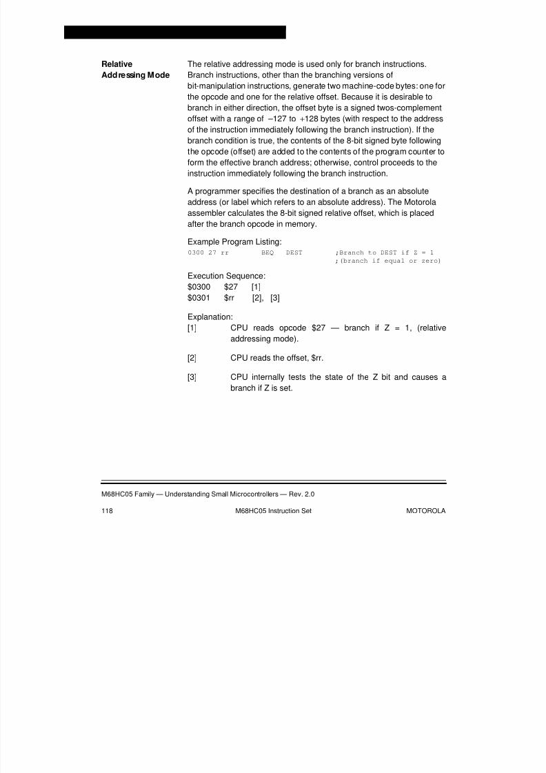
8/2/2019 122 Textbook
http://slidepdf.com/reader/full/122-textbook 118/331
M68HC05 Instruction Set
M68HC05 Family — Understanding Small Microcontrollers — Rev. 2.0
118 M68HC05 Instruction Set MOTOROLA
Relative
Addressing Mode
The relative addressing mode is used only for branch instructions.
Branch instructions, other than the branching versions of
bit-manipulation instructions, generate two machine-code bytes: one for
the opcode and one for the relative offset. Because it is desirable to
branch in either direction, the offset byte is a signed twos-complement
offset with a range of –127 to +128 bytes (with respect to the address
of the instruction immediately following the branch instruction). If the
branch condition is true, the contents of the 8-bit signed byte following
the opcode (offset) are added to the contents of the program counter to
form the effective branch address; otherwise, control proceeds to the
instruction immediately following the branch instruction.
A programmer specifies the destination of a branch as an absolute
address (or label which refers to an absolute address). The Motorola
assembler calculates the 8-bit signed relative offset, which is placed
after the branch opcode in memory.
Example Program Listing:0300 27 rr BEQ DEST ;Branch to DEST if Z = 1
;(branch if equal or zero)
Execution Sequence:
$0300 $27 [1]
$0301 $rr [2], [3]
Explanation:
[1] CPU reads opcode $27 — branch if Z = 1, (relative
addressing mode).
[2] CPU reads the offset, $rr.
[3] CPU internally tests the state of the Z bit and causes a
branch if Z is set.

8/2/2019 122 Textbook
http://slidepdf.com/reader/full/122-textbook 119/331
M68HC05 Instruction Set
Addressing Modes
M68HC05 Family — Understanding Small Microcontrollers — Rev. 2.0
MOTOROLA M68HC05 Instruction Set 119
The following is a list of all M68HC05 instructions that can use the
relative addressing mode.
Instruction MnemonicBranch if Carry Clear BCC
Branch is Carry Set BCS
Branch if Equal BEQ
Branch if Half-Carry Clear BHCC
Branch if Half-Carry Set BHCS
Branch if Higher BHI
Branch if Higher or Same BHS
Branch if Interrupt Line is High BIH
Branch if Interrupt Line is Low BIL
Branch if Lower BLO
Branch if Lower or Same BLS
Branch if Interrupt Mask is Clear BMC
Branch if Minus BMI
Branch if Interrupt Mask Bit is Set BMS
Branch if Not Equal BNE
Branch if Plus BPL
Branch Always BRABranch if Bit n is Clear BRCLR
Branch if Bit n is Set BRSET
Branch Never BRN
Branch to Subroutine BSR

8/2/2019 122 Textbook
http://slidepdf.com/reader/full/122-textbook 120/331
M68HC05 Instruction Set
M68HC05 Family — Understanding Small Microcontrollers — Rev. 2.0
120 M68HC05 Instruction Set MOTOROLA
BitTest and Branch
Instructions
These instructions use direct addressing mode to specify the location
being tested and relative addressing to specify the branch destination.
This text book treats these instructions as direct addressing mode
instructions. Some older Motorola documents call the addressing mode
of these instructions BTB for bit test and branch.
Instructions
Organized
by Type
Table 11 through Table 14 show the MC68HC05 instruction set
displayed by instruction type.

8/2/2019 122 Textbook
http://slidepdf.com/reader/full/122-textbook 121/331
M 6 8 H C 0 5
F ami l y —
U n d er s t an d i n g S m al l Mi c r o c on t r ol l er s —
R ev .2 . 0
M OT OR OL A
M 6 8 H C 0 5
I n s t r u c t i on S e t
1 2 1
Table 11. Register/Memory Instructions
Addressing Modes
Immediate Direct ExtendedIndexed
(No Offset)Ind
(8-Bit
Function Mnem.Op-
code#
Bytes#
CyclesOp-
code#
Bytes#
CyclesOp-
code#
Bytes#
CyclesOp-
code#
Bytes#
CyclesOp-
code By
Load A from Memory LDA A6 2 2 B6 2 3 C6 3 4 F6 1 3 E6
Load X from Memory LDX AE 2 2 BE 2 3 CE 3 4 FE 1 3 EE
Store A in Memory STA — — — B7 2 4 C7 3 5 F7 1 4 E7
Store X in Memory STX — — — BF 2 4 CF 3 5 FF 1 4 EF
Add Memory to A ADD AB 2 BB 2 3 CB 3 4 FB 1 3 EB
Add Memory andCarry to A
ADC A9 2 2 B9 2 3 C9 3 4 F9 1 3 E9
Subtract Memory SUB A0 2 2 B0 2 3 C0 3 4 F0 1 3 E0
Subtract Memory fromA with Borrow
SBC A2 2 2 B2 2 3 C2 3 4 F2 1 3 E2
AND Memory to A AND A4 2 2 B4 2 3 C4 3 4 F4 1 3 E4
OR Memory with A ORA AA 2 2 BA 2 3 CA 3 4 FA 1 3 EA
Exclusive OR Memorywith A
EOR A8 2 2 B8 2 3 C8 3 4 F8 1 3 E8
Arithmetic Compare Awith Memory
CMP A1 2 2 E11 2 3 C1 3 4 F1 1 3 E1
Arithmetic Compare Xwith Memory
CPX A3 2 2 B3 2 3 C3 3 4 F3 1 3 E3
Bit Test Memory withA (Logical Compare)
BIT A5 2 2 B5 2 3 C5 3 4 F5 1 3 E
Jump Unconditional JMP — — — BC 2 2 CC 3 3 FC 1 2 EC
Jump to Subroutine JSR — — — BD 2 5 CD 3 6 FD 1 5 ED

8/2/2019 122 Textbook
http://slidepdf.com/reader/full/122-textbook 122/331
M 6 8 H C 0 5 F ami l y —
U n d er s t an d i n g S m al l Mi c r o c on t r o
l l er s —
R ev .2 . 0
1 2 2
M 6 8 H C 0 5
I n s t r u c t i on S e t
M OT OR OL A
Table 12. Read/Modify-Write Instructions
Addressing Modes
Inherent (A) Inherent (X) DirectIndexed
(No Offset)
Function Mnem.Op-
code#
Bytes#
CyclesOp-
code#
Bytes#
CyclesOp-
code#
Bytes#
CyclesOp-
code#
Bytes#
Cycl
Increment INC 4C 1 3 5C 1 3 3C 2 5 7C 1 5
Decrement DEC 4A 1 3 5A 1 3 3A 2 5 7A 1 5
Clear CLR 4F 1 3 5F 1 3 3F 2 5 7F 1 5
Complement COM 43 1 3 53 1 3 33 2 5 73 1 5
NegateTwos Complement
NEG 40 1 3 50 1 3 30 2 5 70 1 5
Rotate Left Thru Carry ROL 49 1 3 59 1 3 39 2 5 79 1 5
Rotate Right Thru Carry ROR 46 1 3 56 1 3 36 2 5 76 1 5
Logical Shift Left LSL 48 1 3 58 1 3 38 2 5 78 1 5
Logical Shift Right LSR 44 1 3 54 1 3 34 2 5 74 1 5
Arithmetic Shift Right ASH 47 1 3 57 1 3 37 2 5 77 1 5
Test for Negativeor Zero
TST 4D 1 3 5D 1 3 3D 2 4 7D 1 4
Multiply MUL 42 1 11 — — — — — — — — —
Bit Clear BCLR — — — — — —SeeNote
2 5 — — —
Bit Set BSET — — — — — —SeeNote
2 5 — — —
NOTE: Unlike other read-modify-write instructions, BCLR and BSET use only direct addressing.

8/2/2019 122 Textbook
http://slidepdf.com/reader/full/122-textbook 123/331
M68HC05 Instruction Set
Addressing Modes
M68HC05 Family — Understanding Small Microcontrollers — Rev. 2.0
MOTOROLA M68HC05 Instruction Set 123
Table 13. Branch Instructions
Function Mnemonic
Relative AddressingMode
Opcode #Bytes #Cycles
Branch Always BRA 20 2 3
Branch Never BRN 21 2 3
Branch if Higher BH1 22 2 3
Branch if Lower or Same BLS 23 2 3
Branch if Carry Clear BCC 24 2 3
Branch if Higher or Same(Same as BCC)
BHS 24 2 3
Branch if Carry Set BCS 25 2 3
Branch if Lower(Same as BCS)
BLO 25 2 3
Branch if Not Equal BNE 26 2 3
Branch if Equal BEQ 27 2 3
Branch if Half-Carry Clear BHCC 28 2 3
Branch if Half-Carry Set BHCS 29 2 3
Branch if Plus BPL 2A 2 3
Branch if Minus BMI 2B 2 3
Branch if Interrupt Mask Bit is Clear BMC 2C 2 3
Branch if Interrupt Mask Bit is Set BMS 2D 2 3
Branch if Interrupt Line is Low BIL 2E 2 3
Branch if Interrupt Line is High BIH 2F 2 3
Branch to Subroutine BSR AD 2 6

8/2/2019 122 Textbook
http://slidepdf.com/reader/full/122-textbook 124/331
M68HC05 Instruction Set
M68HC05 Family — Understanding Small Microcontrollers — Rev. 2.0
124 M68HC05 Instruction Set MOTOROLA
Table 14. Control Instructions
Function Mnemonic
Relative AddressingMode
Opcode #Bytes #Cycles
Transfer A to X TAX 97 1 2
Transfer X to A TXA 9F 1 2
Set Carry Bit SEC 99 1 2
Clear Carry Bit CLC 98 1 2
Set Interrupt Mask Bit SEI 9B 1 2
Clear Interrupt Mask Bit CLI 9A 1 2
Software Interrupt SWI 83 1 10
Return from Subroutine RTS 81 1 6
Return from Interrupt RTI 80 1 9
Reset Stack Pointer RSP 9C 1 2
No-Operation NOP 9D 1 2
Stop STOP 8E 1 2
Wait WAIT 8F 1 2
8/2/2019 122 Textbook
http://slidepdf.com/reader/full/122-textbook 125/331
M68HC05 Instruction Set
Instruction Set Summary
M68HC05 Family — Understanding Small Microcontrollers — Rev. 2.0
MOTOROLA M68HC05 Instruction Set 125
Instruction Set Summary
Computers use an operation code or opcode to give instructions to the
CPU. The instruction set for a specific CPU is the set of all opcodes thatthe CPU knows how to execute. For example, the CPU in theMC68HC705J1A MCU can understand 62 basic instructions, some ofwhich have several variations that require separate opcodes. TheM68HC05 Family instruction set includes 210 unique instructionopcodes.
The following is an alphabetical listing of the M68HC05 Familyinstructions available to the user. In listing all the factors necessary toprogram, the table uses these symbols:
Condition Code SymbolsH — Half Carry (Bit 4) ¤ — Test and Set if True,I — Interrupt Mask (Bit 3) Cleared OtherwiseN — Negate (Sign Bit 2) — — Not AffectedZ — Zero (Bit 1) 0 — ClearedC — Carry/Borrow (Bit 0) 1 — Set
Boolean Operators( ) — Contents of (For Example, (M) + — Inclusive OR
Means the Contents ⊕ — Exclusive ORof Memory Location M — — NOT
– — Negation,
← — is loaded with, gets Twos Complement• — Logical AND x — Multiplication
CPU RegistersA — Accumulator PC — Program CounterACCA — Accumulator PCH — PC High ByteCCR — Condition Code Register PCL — PC Low ByteX — Index Register SP — Stack PointerM — Any memory location REL — Relative Address, One Byte
Addressing Modes Abbreviation OperandsInherent INH none
Immediate IMM iiDirect (For Bit DIR dd
Test Instructions) dd rrExtended EXT hh llIndexed 0 Offset IX noneIndexed 1-Byte Offset IX1 ffIndexed 2-Byte Offset IX2 ee ffRelative REL rr

8/2/2019 122 Textbook
http://slidepdf.com/reader/full/122-textbook 126/331
M68HC05 Instruction Set
M68HC05 Family — Understanding Small Microcontrollers — Rev. 2.0
126 M68HC05 Instruction Set MOTOROLA
Table 15. Instruction Set Summary (Sheet 1 of 6)
SourceForm
Operation Description
Effect onCCR
A
d d r e s s
M o d e
O
p c o d e
O
p e r a n d
C y c l e s
H I N Z CADC #opr
ADC opr ADC opr
ADC opr ,X
ADC opr ,XADC ,X
Add with Carry A ← (A) + (M) + (C) ¤ — ¤ ¤ ¤
IMM
DIREXT
IX2
IX1IX
A9
B9C9
D9
E9F9
iidd
hh ll
ee ffff
2
34
5
43
ADD #opr
ADD opr
ADD opr ADD opr ,X
ADD opr ,X
ADD ,X
Add without Carry A ← (A) + (M) ¤ — ¤ ¤ ¤
IMM
DIR
EXTIX2
IX1
IX
AB
BB
CBDB
EB
FB
ii
ddhh ll
ee ff
ff
2
3
45
4
3
AND #opr
AND opr AND opr
AND opr ,XAND opr ,X
AND ,X
Logical AND A ← (A) ∧ (M) — — ¤ ¤ —
IMM
DIREXT
IX2IX1
IX
A4
B4C4
D4E4
F4
ii
ddhh llee ff
ff
2
34
54
3
ASL opr ASLA
ASLX
ASL opr ,X
ASL ,X
Arithmetic Shift Left (Same as LSL) — — ¤ ¤ ¤
DIRINH
INH
IX1
IX
3848
58
68
78
dd
ff
53
3
6
5
ASR opr
ASRAASRX
ASR opr ,XASR ,X
Arithmetic Shift Right — — ¤ ¤ ¤
DIR
INHINH
IX1IX
37
4757
6777
dd
ff
5
33
65
BCC rel Branch if Carry Bit Clear PC ← (PC) + 2 + rel ? C = 0 — — — — — REL 24 rr 3
BCLR n opr Clear Bit n Mn ← 0 — — — — —
DIR (b0)
DIR (b1)
DIR (b2)DIR (b3)
DIR (b4)
DIR (b5)DIR (b6)
DIR (b7)
11
13
1517
19
1B1D
1F
dd
dd
dddd
dd
dddd
dd
5
5
55
5
55
5
BCS rel Branch if Carry Bit Set (Same as BLO) PC ← (PC) + 2 + rel ? C = 1 — — — — — REL 25 rr 3
BEQ rel Branch if Equal PC ← (PC) + 2 + rel ? Z = 1 — — — — — REL 27 rr 3
BHCC rel Branch if Half-Carry Bit Clear PC ← (PC) + 2 + rel ? H = 0 — — — — — REL 28 rr 3BHCS rel Branch if Half-Carry Bit Set PC ← (PC) + 2 + rel ? H = 1 — — — — — REL 29 rr 3
BHI rel Branch if Higher PC ← (PC) + 2 + rel ? C ∨ Z = 0 — — — — — REL 22 rr 3
BHS rel Branch if Higher or Same PC ← (PC) + 2 + rel ? C = 0 — — — — — REL 24 rr 3
BIH rel Branch if IRQ Pin High PC ← (PC) + 2 + rel ? IRQ = 1 — — — — — REL 2F rr 3
BIL rel Branch if IRQ Pin Low PC ← (PC) + 2 + rel ? IRQ = 0 — — — — — REL 2E rr 3
C
b0b7
0
b0b7
C

8/2/2019 122 Textbook
http://slidepdf.com/reader/full/122-textbook 127/331
M68HC05 Instruction Set
Instruction Set Summary
M68HC05 Family — Understanding Small Microcontrollers — Rev. 2.0
MOTOROLA M68HC05 Instruction Set 127
BIT #opr
BIT opr BIT opr
BIT opr ,X
BIT opr ,X
BIT ,X
Bit Test Accumulator with Memory Byte (A) ∧ (M) — — ¤ ¤ —
IMM
DIREXT
IX2
IX1
IX
A5
B5C5
D5
E5
F5
iidd
hh ll
ee ffff
2
34
5
4
3
BLO rel Branch if Lower (Same as BCS) PC ← (PC) + 2 + rel ? C = 1 — — — — — REL 25 rr 3
BLS rel Branch if Lower or Same PC ← (PC) + 2 + rel ? C ∨ Z = 1 — — — — — REL 23 rr 3
BMC rel Branch if Interrupt Mask Clear PC ← (PC) + 2 + rel ? I = 0 — — — — — REL 2C rr 3
BMI rel Branch if Minus PC ← (PC) + 2 + rel ? N = 1 — — — — — REL 2B rr 3
BMS rel Branch if Interrupt Mask Set PC ← (PC) + 2 + rel ? I = 1 — — — — — REL 2D rr 3
BNE rel Branch if Not Equal PC ← (PC) + 2 + rel ? Z = 0 — — — — — REL 26 rr 3
BPL rel Branch if Plus PC ← (PC) + 2 + rel ? N = 0 — — — — — REL 2A rr 3
BRA rel Branch Always PC ← (PC) + 2 + rel ? 1 = 1 — — — — — REL 20 rr 3
BRCLR n opr rel Branch if Bit n Clear PC ← (PC) + 2 + rel ? Mn = 0 — — — — ¤
DIR (b0)
DIR (b1)
DIR (b2)
DIR (b3)DIR (b4)
DIR (b5)
DIR (b6)DIR (b7)
01
03
05
0709
0B
0D0F
dd rr
dd rr
dd rr
dd rrdd rr
dd rr
dd rrdd rr
5
5
5
55
5
55
BRN rel Branch Never PC ← (PC) + 2 + rel ? 1 = 0 — — — — — REL 21 rr 3
BRSET n opr rel Branch if Bit n Set PC ← (PC) + 2 + rel ? Mn = 1 — — — — ¤
DIR (b0)DIR (b1)
DIR (b2)DIR (b3)DIR (b4)
DIR (b5)
DIR (b6)DIR (b7)
0002
040608
0A
0C0E
dd rrdd rr
dd rrdd rrdd rr
dd rr
dd rrdd rr
55
555
5
55
BSET n opr Set Bit n Mn ← 1 — — — — —
DIR (b0)DIR (b1)
DIR (b2)
DIR (b3)DIR (b4)
DIR (b5)
DIR (b6)DIR (b7)
1012
14
1618
1A
1C1E
dddd
dd
dddd
dd
dddd
55
5
55
5
55
BSR rel Branch to Subroutine
PC ← (PC) + 2; push (PCL)
SP ← (SP) – 1; push (PCH)SP ← (SP) – 1
PC ← (PC) + rel
— — — — — REL AD rr 6
CLC Clear Carry Bit C ← 0 — — — — 0 INH 98 2
CLI Clear Interrupt Mask I ← 0 — 0 — — — INH 9A 2
Table 15. Instruction Set Summary (Sheet 2 of 6)
SourceForm
Operation Description
Effect onCCR
A d d r e s s
M o d e
O p c o d e
O p e r a n d
C y c l e s
H I N Z C

8/2/2019 122 Textbook
http://slidepdf.com/reader/full/122-textbook 128/331
M68HC05 Instruction Set
M68HC05 Family — Understanding Small Microcontrollers — Rev. 2.0
128 M68HC05 Instruction Set MOTOROLA
CLR opr CLRA
CLRX
CLR opr ,X
CLR ,X
Clear Byte
M ← $00A ← $00
X ← $00
M ← $00
M ← $00
— — 0 1 —
DIRINH
INH
IX1
IX
3F4F
5F
6F
7F
dd
ff
53
3
6
5
CMP #opr
CMP opr
CMP opr CMP opr ,X
CMP opr ,X
CMP ,X
Compare Accumulator with Memory Byte (A) – (M) — — ¤ ¤ ¤
IMM
DIR
EXTIX2
IX1
IX
A1
B1
C1D1
E1
F1
ii
ddhh ll
ee ff
ff
2
3
45
4
3
COM opr
COMA
COMXCOM opr ,X
COM ,X
Complement Byte (One’s Complement)
M ← (M) = $FF – (M)
A ← (A) = $FF – (A)
X ← (X) = $FF – (X)M ← (M) = $FF – (M)
M ← (M) = $FF – (M)
— — ¤ ¤ 1
DIR
INH
INHIX1
IX
33
43
5363
73
dd
ff
5
3
36
5
CPX #opr CPX opr
CPX opr
CPX opr ,X
CPX opr ,XCPX ,X
Compare Index Register with Memory Byte (X) – (M) — — ¤ ¤ ¤
IMMDIR
EXT
IX2
IX1IX
A3B3
C3
D3
E3F3
ii
dd
hh llee ff
ff
23
4
5
43
DEC opr
DECADECX
DEC opr ,X
DEC ,X
Decrement Byte
M ← (M) – 1
A ← (A) – 1X ← (X) – 1
M ← (M) – 1
M ← (M) – 1
— — ¤ ¤ —
DIR
INHINH
IX1
IX
3A
4A5A
6A
7A
dd
ff
5
33
6
5
EOR #opr
EOR opr
EOR opr EOR opr ,X
EOR opr ,X
EOR ,X
EXCLUSIVE OR Accumulator with Memory Byte A ← (A) ⊕ (M) — — ¤ ¤ —
IMM
DIR
EXTIX2
IX1
IX
A8
B8
C8D8
E8
F8
ii
ddhh ll
ee ff
ff
2
3
45
4
3
INC opr
INCA
INCXINC opr ,X
INC ,X
Increment Byte
M ← (M) + 1
A ← (A) + 1
X ← (X) + 1M ← (M) + 1
M ← (M) + 1
— — ¤ ¤ —
DIR
INH
INHIX1
IX
3C
4C
5C6C
7C
dd
ff
5
3
36
5
JMP opr
JMP opr JMP opr ,X
JMP opr ,X
JMP ,X
Unconditional Jump PC ← Jump Address — — — — —
DIR
EXTIX2
IX1
IX
BC
CCDC
EC
FC
dd
hh llee ff
ff
2
34
3
2
Table 15. Instruction Set Summary (Sheet 3 of 6)
SourceForm
Operation Description
Effect onCCR
A d d r e s s
M o d e
O p c o d e
O p e r a n d
C y c l e s
H I N Z C

8/2/2019 122 Textbook
http://slidepdf.com/reader/full/122-textbook 129/331
M68HC05 Instruction Set
Instruction Set Summary
M68HC05 Family — Understanding Small Microcontrollers — Rev. 2.0
MOTOROLA M68HC05 Instruction Set 129
JSR opr
JSR opr JSR opr ,X
JSR opr ,X
JSR ,X
Jump to Subroutine
PC ← (PC) + n (n = 1, 2, or 3)
Push (PCL); SP ← (SP) – 1Push (PCH); SP ← (SP) – 1
PC ← Effective Address
— — — — —
DIR
EXTIX2
IX1
IX
BD
CDDD
ED
FD
ddhh ll
ee ff
ff
5
67
6
5
LDA #opr LDA opr
LDA opr
LDA opr ,X
LDA opr ,XLDA ,X
Load Accumulator with Memory Byte A ← (M) — — ¤ ¤ —
IMMDIR
EXT
IX2
IX1IX
A6B6
C6
D6
E6F6
ii
dd
hh llee ff
ff
23
4
5
43
LDX #opr
LDX opr
LDX opr LDX opr ,X
LDX opr ,X
LDX ,X
Load Index Register with Memory Byte X ← (M) — — ¤ ¤ —
IMM
DIR
EXTIX2
IX1
IX
AE
BE
CEDE
EE
FE
iidd
hh llee ff
ff
2
3
45
4
3
LSL opr
LSLA
LSLXLSL opr ,X
LSL ,X
Logical Shift Left (Same as ASL) — — ¤ ¤ ¤
DIR
INH
INHIX1
IX
38
48
5868
78
dd
ff
5
3
36
5
LSR opr
LSRA
LSRXLSR opr ,X
LSR ,X
Logical Shift Right — — 0 ¤ ¤
DIR
INH
INHIX1
IX
34
44
5464
74
dd
ff
5
3
36
5
MUL Unsigned Multiply X : A ← (X) × (A) 0 — — — 0 INH 42 11
NEG opr
NEGA
NEGX
NEG opr ,XNEG ,X
Negate Byte (Two’s Complement)
M ← –(M) = $00 – (M)
A ← –(A) = $00 – (A)
X ← –(X) = $00 – (X)
M ← –(M) = $00 – (M)M ← –(M) = $00 – (M)
— — ¤ ¤ ¤
DIR
INH
INH
IX1IX
30
40
50
6070
dd
ff
5
3
3
65
NOP No Operation — — — — — INH 9D 2
ORA #opr ORA opr
ORA opr
ORA opr ,X
ORA opr ,X
ORA ,X
Logical OR Accumulator with Memory A ← (A) ∨ (M) — — ¤ ¤ —
IMMDIR
EXT
IX2
IX1
IX
AABA
CA
DA
EA
FA
ii
dd
hh llee ff
ff
23
4
5
4
3
ROL opr
ROLAROLX
ROL opr ,X
ROL ,X
Rotate Byte Left through Carry Bit — — ¤ ¤ ¤
DIR
INHINH
IX1
IX
39
4959
69
79
dd
ff
5
33
6
5
Table 15. Instruction Set Summary (Sheet 4 of 6)
SourceForm
Operation Description
Effect onCCR
A d d r e s s
M o d e
O p c o d e
O p e r a n d
C y c l e s
H I N Z C
C
b0b7
0
b0b7
C0
C
b0b7
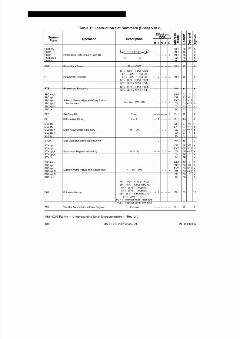
8/2/2019 122 Textbook
http://slidepdf.com/reader/full/122-textbook 130/331
M68HC05 Instruction Set
M68HC05 Family — Understanding Small Microcontrollers — Rev. 2.0
130 M68HC05 Instruction Set MOTOROLA
ROR opr RORA
RORX
ROR opr ,X
ROR ,X
Rotate Byte Right through Carry Bit — — ¤ ¤ ¤
DIRINH
INH
IX1
IX
3646
56
66
76
dd
ff
53
3
6
5
RSP Reset Stack Pointer SP ← $00FF — — — — — INH 9C 2
RTI Return from Interrupt
SP ← (SP) + 1; Pull (CCR)SP ← (SP) + 1; Pull (A)
SP ← (SP) + 1; Pull (X)
SP ← (SP) + 1; Pull (PCH)
SP ← (SP) + 1; Pull (PCL)
¤ ¤ ¤ ¤ ¤ INH 80 9
RTS Return from SubroutineSP ← (SP) + 1; Pull (PCH)SP ← (SP) + 1; Pull (PCL)
— — — — — INH 81 6
SBC #opr
SBC opr SBC opr
SBC opr ,X
SBC opr ,XSBC ,X
Subtract Memory Byte and Carry Bit from
AccumulatorA ← (A) – (M) – (C) — — ¤ ¤ ¤
IMM
DIREXT
IX2
IX1IX
A2
B2C2
D2
E2F2
iidd
hh ll
ee ffff
2
34
5
43
SEC Set Carry Bit C ← 1 — — — — 1 INH 99 2
SEI Set Interrupt Mask I ← 1 — 1 — — — INH 9B 2
STA opr
STA opr
STA opr ,XSTA opr ,X
STA ,X
Store Accumulator in Memory M ← (A) — — ¤ ¤ —
DIR
EXT
IX2IX1
IX
B7
C7
D7E7
F7
ddhh ll
ee ff
ff
4
5
65
4
STOP Stop Oscillator and Enable IRQ Pin — 0 — — — INH 8E 2
STX opr STX opr
STX opr ,X
STX opr ,XSTX ,X
Store Index Register In Memory M ← (X) — — ¤ ¤ —
DIREXT
IX2
IX1IX
BFCF
DF
EFFF
dd
hh ll
ee ffff
45
6
54
SUB #opr
SUB opr
SUB opr SUB opr ,X
SUB opr ,X
SUB ,X
Subtract Memory Byte from Accumulator A ← (A) – (M) — — ¤ ¤ ¤
IMM
DIR
EXTIX2
IX1
IX
A0
B0
C0D0
E0
F0
ii
ddhh ll
ee ff
ff
2
3
45
4
3
SWI Software Interrupt
PC ← (PC) + 1; Push (PCL)
SP ← (SP) – 1; Push (PCH)
SP ← (SP) – 1; Push (X)SP ← (SP) – 1; Push (A)
SP ← (SP) – 1; Push (CCR)
SP ← (SP) – 1; I ← 1
PCH ← Interrupt Vector High BytePCL ← Interrupt Vector Low Byte
— 1 — — — INH 83 10
TAX Transfer Accumulator to Index Register X ← (A) — — — — — INH 97 2
Table 15. Instruction Set Summary (Sheet 5 of 6)
SourceForm
Operation Description
Effect onCCR
A d d r e s s
M o d e
O p c o d e
O p e r a n d
C y c l e s
H I N Z C
b0b7
C

8/2/2019 122 Textbook
http://slidepdf.com/reader/full/122-textbook 131/331
M68HC05 Instruction Set
Instruction Set Summary
M68HC05 Family — Understanding Small Microcontrollers — Rev. 2.0
MOTOROLA M68HC05 Instruction Set 131
TST opr TSTA
TSTX
TST opr ,X
TST ,X
Test Memory Byte for Negative or Zero (M) – $00 — — ¤ ¤ —
DIRINH
INH
IX1
IX
3D4D
5D
6D
7D
dd
ff
43
3
5
4
TXA Transfer Index Register to Accumulator A ← (X) — — — — — INH 9F 2
WAIT Stop CPU Clock and Enable Interrupts — 0 — — — INH 8F 2
A Accumulator opr Operand (one or two bytes)C Carry/borrow flag PC Program counter
CCR Condition code register PCH Program counter high byte
dd Direct address of operand PCL Program counter low bytedd rr Direct address of operand and relative offset of branch instruction REL Relative addressing mode
DIR Direct addressing mode rel Relative program counter offset byteee ff High and low bytes of offset in indexed, 16-bit offset addressing rr Relative program counter offset byte
EXT Extended addressing mode SP Stack pointerff Offset byte in indexed, 8-bit offset addressing X Index register
H Half-carry flag Z Zero flag
hh ll High and low bytes of operand address in extended addressing # Immediate valueI Interrupt mask • Logical AND
ii Immediate operand byte + Logical OR
IMM Immediate addressing mode ⊕ Logical EXCLUSIVE ORINH Inherent addressing mode ( ) Contents of
IX Indexed, no offset addressing mode –( ) Negation (twos complement)
IX1 Indexed, 8-bit offset addressing mode ← Loaded withIX2 Indexed, 16-bit offset addressing mode ? If
M Memory location : Concatenated with
N Negative flag ¤ Set or cleared
n Any bit — Not affected
Table 15. Instruction Set Summary (Sheet 6 of 6)
SourceForm
Operation Description
Effect onCCR
A d d r e s s
M o d e
O p c o d e
O p e r a n d
C y c l e s
H I N Z C

8/2/2019 122 Textbook
http://slidepdf.com/reader/full/122-textbook 132/331
M 6 8H C 0 5In s tr u c ti on
M 6 8 H C 0 5 F ami l y —
U n d er s t a
n d i n g S m al l Mi c r o c on t r ol l er s —
R ev .2 . 0
1 3 2
M 6 8 H C 0 5 I n s t r u c t i on S e t
M OT OR OL A
Table 16. M68HC05 Instruction Set Opcode Map
Bit Manipulation Branch Read-Modify-Write Control Register/Memory
DIR DIR REL DIR INH INH IX1 IX INH INH IMM DIR EXT IX2 IX1 IX
0 1 2 3 4 5 6 7 8 9 A B C D E F
05
BRSET03 DIR
5BSET0
2 DIR
3BRA
2 REL
5NEG
2 DIR
3NEGA
1 INH
3NEGX
1 INH
6NEG
2 IX1
5NEG
1 IX
9RTI
1 INH
2SUB
2 IMM
3SUB
2 DIR
4SUB
3 EXT
5SUB
3 IX2
4SUB
2 IX1
3SUB
1 IX0
15
BRCLR03 DIR
5BCLR0
2 DIR
3BRN
2 REL
6RTS
1 INH
2CMP
2 IMM
3CMP
2 DIR
4CMP
3 EXT
5CMP
3 IX2
4CMP
2 IX1
3CMP
1 IX1
25
BRSET13 DIR
5BSET1
2 DIR
3BHI
2 REL
11MUL
1 INH
2SBC
2 IMM
3SBC
2 DIR
4SBC
3 EXT
5SBC
3 IX2
4SBC
2 IX1
3SBC
1 IX2
3
5
BRCLR13 DIR
5
BCLR12 DIR
3
BLS2 REL
5
COM2 DIR
3
COMA1 INH
3
COMX1 INH
6
COM2 IX1
5
COM1 IX
10
SWI1 INH
2
CPX2 IMM
3
CPX2 DIR
4
CPX3 EXT
5
CPX3 IX2
4
CPX2 IX1
3
CPX1 IX 3
45
BRSET23 DIR
5BSET2
2 DIR
3BCC
2 REL
5LSR
2 DIR
3LSRA
1 INH
3LSRX
1 INH
6LSR
2 IX1
5LSR
1 IX
2AND
2 IMM
3AND
2 DIR
4AND
3 EXT
5AND
3 IX2
4AND
2 IX1
3AND
1 IX4
55
BRCLR23 DIR
5BCLR2
2 DIR
3BCS/BLO2 REL
2BIT
2 IMM
3BIT
2 DIR
4BIT
3 EXT
5BIT
3 IX2
4BIT
2 IX1
3BIT
1 IX5
65
BRSET33 DIR
5BSET3
2 DIR
3BNE
2 REL
5ROR
2 DIR
3RORA
1 INH
3RORX
1 INH
6ROR
2 IX1
5ROR
1 IX
2LDA
2 IMM
3LDA
2 DIR
4LDA
3 EXT
5LDA
3 IX2
4LDA
2 IX1
3LDA
1 IX6
75
BRCLR33 DIR
5BCLR3
2 DIR
3BEQ
2 REL
5ASR
2 DIR
3ASRA
1 INH
3ASRX
1 INH
6ASR
2 IX1
5ASR
1 IX
2TAX
1 INH
4STA
2 DIR
5STA
3 EXT
6STA
3 IX2
5STA
2 IX1
4STA
1 IX7
85
BRSET43 DIR
5BSET4
2 DIR
3BHCC
2 REL
5ASL/LSL
2 DIR
3ASLA/LSLA1 INH
3ASLX/LSLX1 INH
6ASL/LSL
2 IX1
5ASL/LSL
1 IX
2CLC
1 INH
2EOR
2 IMM
3EOR
2 DIR
4EOR
3 EXT
5EOR
3 IX2
4EOR
2 IX1
3EOR
1 IX8
95
BRCLR43 DIR
5BCLR4
2 DIR
3BHCS
2 REL
5ROL
2 DIR
3ROLA
1 INH
3ROLX
1 INH
6ROL
2 IX1
5ROL
1 IX
2SEC
1 INH
2ADC
2 IMM
3ADC
2 DIR
4ADC
3 EXT
5ADC
3 IX2
4ADC
2 IX1
3ADC
1 IX9
A5
BRSET53 DIR
5BSET5
2 DIR
3BPL
2 REL
5DEC
2 DIR
3DECA
1 INH
3DECX
1 INH
6DEC
2 IX1
5DEC
1 IX
2CLI
1 INH
2ORA
2 IMM
3ORA
2 DIR
4ORA
3 EXT
5ORA
3 IX2
4ORA
2 IX1
3ORA
1 IXA
B5
BRCLR53 DIR
5BCLR5
2 DIR
3BMI
2 REL
2SEI
1 INH
2ADD
2 IMM
3ADD
2 DIR
4ADD
3 EXT
5ADD
3 IX2
4ADD
2 IX1
3ADD
1 IXB
C5
BRSET63 DIR
5BSET6
2 DIR
3BMC
2 REL
5INC
2 DIR
3INCA
1 INH
3INCX
1 INH
6INC
2 IX1
5INC
1 IX
2RSP
1 INH
2JMP
2 DIR
3JMP
3 EXT
4JMP
3 IX2
3JMP
2 IX1
2JMP
1 IXC
D5
BRCLR63 DIR
5BCLR6
2 DIR
3BMS
2 REL
4TST
2 DIR
3TSTA
1 INH
3TSTX
1 INH
5TST
2 IX1
4TST
1 IX
2NOP
1 INH
6BSR
2 REL
5JSR
2 DIR
6JSR
3 EXT
7JSR
3 IX2
6JSR
2 IX1
5JSR
1 IXD
E5
BRSET73 DIR
5BSET7
2 DIR
3BIL
2 REL
2STOP
1 INH
2LDX
2 IMM
3LDX
2 DIR
4LDX
3 EXT
5LDX
3 IX2
4LDX
2 IX1
3LDX
1 IXE
F5
BRCLR73 DIR
5BCLR7
2 DIR
3BIH
2 REL
5CLR
2 DIR
3CLRA
1 INH
3CLRX
1 INH
6CLR
2 IX1
5CLR
1 IX
2WAIT
1 INH
2TXA
1 INH
4STX
2 DIR
5STX
3 EXT
6STX
3 IX2
5STX
2 IX1
4STX
1 IXF
INH = Inherent REL = RelativeIMM = Immediate IX = Indexed, No OffsetDIR = Direct IX1 = Indexed, 8-Bit OffsetEXT = Extended IX2 = Indexed, 16-Bit Offset
0 MSB of Opcode in Hexadecimal
LSB of Opcode in Hexadecimal 05
BRSET03 DIR
Number of CyclesOpcode MnemonicNumber of Bytes/Addressing Mode
LSB
MSB
LSB
MSB
LSB
MSB

8/2/2019 122 Textbook
http://slidepdf.com/reader/full/122-textbook 133/331
M68HC05 Instruction Set
Review
M68HC05 Family — Understanding Small Microcontrollers — Rev. 2.0
MOTOROLA M68HC05 Instruction Set 133
Review
CPU Registers The five CPU registers in the M68HC05 MCUs are not locations in thememory map. The programming model for the CPU shows the five
CPU registers.
• The accumulator (A) is an 8-bit general-purpose register.
• The index register (X) is an 8-bit pointer register.
• The stack pointer (SP) is a pointer register that is decremented
automatically as data is pushed onto the stack and incremented
as data is pulled off of the stack.
• The program counter (PC) has as many bits as there areaddress lines. The program counter always points at the next
instruction or piece of data the CPU will use.
• The condition code register (CCR) contains the four arithmetic
result flags H, N, Z, and C and the interrupt mask (disable) control
bit I.
Addressing Modes The M68HC05 CPU has six addressing modes that determine how the
CPU will get the operand(s) needed to complete each instruction. TheM68HC05 CPU has only 62 mnemonic instructions. There are 210
instruction opcodes because each different addressing mode variation
of an instruction must have a unique opcode.
• In immediate addressing mode, the operand for the instruction is
the byte immediately after the opcode.
• In inherent addressing mode, the CPU needs no operands from
memory. The operands, if any, are the registers or stacked data
values.
• In extended addressing mode, the 16-bit address of the operand
is located in the next two memory bytes after the instruction
opcode.

8/2/2019 122 Textbook
http://slidepdf.com/reader/full/122-textbook 134/331
M68HC05 Instruction Set
M68HC05 Family — Understanding Small Microcontrollers — Rev. 2.0
134 M68HC05 Instruction Set MOTOROLA
• In direct addressing mode, the low order eight bits of the address
of the operand are located in the next byte of memory after the
opcode and the high order byte of the address is assumed to be
$00. This mode is more efficient than the extended addressing
mode because the high order address byte is not explicitly
included in the program.
• In indexed addressing mode, the current value of the index
register is added to a 0-, 1-, or 2-byte offset in the next 0, 1, or 2
memory locations after the opcode to form a pointer to the address
of the operand in memory.
• Relative addressing mode is used for conditional branch
instructions. The byte after the opcode is a signed offset value
between –128 and +127. If the condition of the branch is true, the
offset is added to the program counter value to get the address
where the CPU will fetch the next program instruction.
Instruction
Execution
Each opcode tells the CPU the operation to be performed and the
addressing mode to be used to address any operands needed to
complete the instruction. The cycle-by-cycle explanations of example
instructions under each addressing mode provide a view of the tiny
simple steps that make up an instruction.
8/2/2019 122 Textbook
http://slidepdf.com/reader/full/122-textbook 135/331
M68HC05 Family — Understanding Small Microcontrollers — Rev. 2.0
MOTOROLA Programming 135
Programming
Contents
Introduction . . . . . . . . . . . . . . . . . . . . . . . . . . . . . . . . . . . . . . . . . . . .136
Writing a Simple Program . . . . . . . . . . . . . . . . . . . . . . . . . . . . . . . . .136
Flowchart. . . . . . . . . . . . . . . . . . . . . . . . . . . . . . . . . . . . . . . . . . . .137
Mnemonic Source Code . . . . . . . . . . . . . . . . . . . . . . . . . . . . . . . . . .139
Software Delay Program . . . . . . . . . . . . . . . . . . . . . . . . . . . . . . . . . .141
Assembler Listing . . . . . . . . . . . . . . . . . . . . . . . . . . . . . . . . . . . . . . .143
Object Code File . . . . . . . . . . . . . . . . . . . . . . . . . . . . . . . . . . . . . .147
Assembler Directives. . . . . . . . . . . . . . . . . . . . . . . . . . . . . . . . . . . . .149
Originate (ORG) . . . . . . . . . . . . . . . . . . . . . . . . . . . . . . . . . . . . . .149
Equate (EQU) . . . . . . . . . . . . . . . . . . . . . . . . . . . . . . . . . . . . . . . .149
Form Constant Byte (FCB) . . . . . . . . . . . . . . . . . . . . . . . . . . . . . .150
Form Double Byte (FDB). . . . . . . . . . . . . . . . . . . . . . . . . . . . . . . .150
Reserve Memory Byte (RMB) . . . . . . . . . . . . . . . . . . . . . . . . . . . . 151
Set Default Number Base to Decimal . . . . . . . . . . . . . . . . . . . . . .152
Instruction Set Dexterity . . . . . . . . . . . . . . . . . . . . . . . . . . . . . . . . . .153
Application Development. . . . . . . . . . . . . . . . . . . . . . . . . . . . . . . . . .154
Review. . . . . . . . . . . . . . . . . . . . . . . . . . . . . . . . . . . . . . . . . . . . . . . .156

8/2/2019 122 Textbook
http://slidepdf.com/reader/full/122-textbook 136/331
Programming
M68HC05 Family — Understanding Small Microcontrollers — Rev. 2.0
136 Programming MOTOROLA
Introduction
This chapter discusses how to plan and write computer programs. We
will learn how to prepare flowcharts, write assembly language programs,and use a text editor or word processor to write computer programs.
Next, a programming tool called an assembler is used to translate the
program into a form the computer can use. Programming tools are
computer programs for personal computers that help in the development
of microcontroller computer programs. We will discuss assemblers,
simulators, and a few other useful development tools.
Writing a Simple Program
At this point, we will write a short program in mnemonic form and
translate it into machine code. These are the steps:
• The first step will be to plan the program and document this plan
with a flowchart.
• Next we will write instruction mnemonics for each block in the
flowchart.
• Finally, we will use an assembler to translate our example
program into the codes the computer needs to execute the
program.
Our program will read the state of a switch connected to an input pin.
When the switch is closed, the program will cause an LED (light-emitting
diode) connected to an output pin to light for about one second and then
go out. The LED will not light again until the switch has been released
and closed again. The length of time the switch is held closed will not
affect the length of time the LED is lighted.

8/2/2019 122 Textbook
http://slidepdf.com/reader/full/122-textbook 137/331
Programming
Writing a Simple Program
M68HC05 Family — Understanding Small Microcontrollers — Rev. 2.0
MOTOROLA Programming 137
Although this program is simple, it demonstrates the most common
elements of any MCU application program:
• First, it demonstrates how a program can sense input signals such
as switch closures.
• Second, this is an example of a program controlling an output
signal.
• Third, the LED on-time of about one second demonstrates one
way a program can be used to measure real time.
Because the algorithm is sufficiently complicated, it cannot be
accomplished in a trivial manner with discrete components. At minimum,
a one-shot IC (integrated circuit) with external timing components would
be required. This example demonstrates that an MCU and auser-defined program (software) can replace complex circuits.
Flowchart Figure 30 is a flowchart of the example program. Flowcharts are often
used as planning tools for writing software programs because they show
the function and flow of the program under development. The
importance of notes, comments, and documentation for software cannot
be over-emphasized. Just as you would not consider a circuit-board
design complete until there is a schematic diagram, parts list, and
assembly drawing, you should not consider a program completeuntil there is a commented listing and a comprehensive
explanation of the program such as a flowchart.

8/2/2019 122 Textbook
http://slidepdf.com/reader/full/122-textbook 138/331
Programming
M68HC05 Family — Understanding Small Microcontrollers — Rev. 2.0
138 Programming MOTOROLA
Figure 30. Example Flowchart
BEGIN
READ SWITCH
YES
NOCLOSED ?
SET INITIAL CONDITIONS:
PORT A BIT 7 = 1 (LED OFF)MAKE PORT A BIT 7 AN OUTPUT
DELAY TO DEBOUNCE
TURN ON LED
DELAY 1 SECOND
TURN OFF LED
YES
NO
SWITCH
STILL CLOSED ?
DELAY TO DEBOUNCE

8/2/2019 122 Textbook
http://slidepdf.com/reader/full/122-textbook 139/331
Programming
Mnemonic Source Code
M68HC05 Family — Understanding Small Microcontrollers — Rev. 2.0
MOTOROLA Programming 139
Mnemonic Source Code
Once the flowchart or plan is completed, the programmer develops a
series of assembly language instructions to accomplish the function(s)called for in each block of the plan. The programmer is limited to
selecting instructions from the instruction set for the CPU being used (in
this case the M68HC05). The programmer writes instructions in a
mnemonic form that is easy to understand. Figure 31 shows the
mnemonic source code next to the flowchart of our example program
so you can see what CPU instructions are used to accomplish each
block of the flowchart. The meanings of the mnemonics used in the right
side of Figure 31 can be found in Instruction Set Details or in
Instruction Set Summary.
During development of the program instructions, it was noticed that a
time delay was needed in three places. A subroutine was developed
that generates a 50-ms delay. This subroutine is used directly in two
places (for switch debouncing) and makes the 1-second delay easier to
produce. To keep this figure simple, the comments that would usually be
included within the source program for documentation are omitted. The
comments will be shown in the completed program in Listing 3.
Assembler Listing.

8/2/2019 122 Textbook
http://slidepdf.com/reader/full/122-textbook 140/331
Programming
M68HC05 Family — Understanding Small Microcontrollers — Rev. 2.0
140 Programming MOTOROLA
Figure 31. Flowchart and Mnemonics
INIT LDA #$80
MNEMONIC PROGRAM
STA PORTA
STA DDRA
TOP LDA PORTA
BEQ TOP
JSR DLY50
BCLR 7,PORTA
LDA #20
DLYLP JSR DLY50
DECA
BNE DLYLP
BSET 7,PORTA
OFFLP BRSET 0,PORTA,OFFLP
JSR DLY50
BRA TOP
BEGIN
READ SWITCH
YES
NOCLOSED ?
DELAY TO DEBOUNCE
TURN ON LED
DELAY 1 SECOND
TURN OFF LED
YES
NO
SWITCHSTILL CLOSED ?
DELAY TO DEBOUNCE
FLOWCHART
SET INITIAL CONDITIONS:
PORT A BIT 7 = 1 (LED OFF)
MAKE PORT A BIT 7 AN OUTPUT
AND #$01

8/2/2019 122 Textbook
http://slidepdf.com/reader/full/122-textbook 141/331
Programming
Software Delay Program
M68HC05 Family — Understanding Small Microcontrollers — Rev. 2.0
MOTOROLA Programming 141
Software Delay Program
Figure 32 shows an expanded flowchart of the 50-ms delay subroutine.
A subroutine is a relatively short program that performs some commonlyrequired function. Even if the function needs to be performed many times
in the course of a program, the subroutine only has to be written once.
Each place where this function is needed, the programmer would call the
subroutine with a branch-to-subroutine (BSR) or jump-to-subroutine
(JSR) instruction.
Figure 32. Delay Routine Flowchart and Mnemonics
START
SUBROUTINE
SAVE ACCUMULATOR
YES
NO COUNT
EXPIRED ?
LOAD VALUE
CORRESPONDING TO 50 ms
DECREMENT COUNT
RESTORE
ACCUMULATOR
RETURN FROMSUBROUTINE
DLY50 STA TEMP1 4
FLOWCHART MNEMONIC PROGRAM INSTRUCTION
TIME (CYCLES)
LDA #65 2
OUTLP CLRX 3
INNRLP DECX 3
BNE INNRLP 3
DECA 3
BNE OUTLP 3
LDA TEMP1 3
RTS 6
6 (JSR)
[1]
[2]
[1] – INNRLP is executed 256 times per pass through outer loop.
[2] – OUTLP is executed 65 times.

8/2/2019 122 Textbook
http://slidepdf.com/reader/full/122-textbook 142/331
Programming
M68HC05 Family — Understanding Small Microcontrollers — Rev. 2.0
142 Programming MOTOROLA
Before starting to execute the instructions in the subroutine, the address
of the instruction that follows the JSR (or BSR) is stored automatically on
the stack in temporary RAM memory locations. When the CPU finishes
executing the instructions within the subroutine, a
return-from-subroutine (RTS) instruction is performed as the last
instruction in the subroutine. The RTS instruction causes the CPU to
recover the previously saved return address; thus, the CPU continues
the program with the instruction following the JSR (or BSR) instruction
that originally called the subroutine.
The delay routine of Figure 32 involves an inner loop (INNRLP) within
another loop (OUTLP). The inner loop consists of two instructions
executed 256 times before X reaches $00 and the BNE branch condition
fails. This amounts to six cycles at 500 ns per cycle times 256, which
equals 0.768 ms for the inner loop. The outer loop executes 65 times.
The total execution time for the outer loop is 65(1536+9) or
65(1545) = 100,425 cycles or 50.212 ms. The miscellaneous
instructions in this routine other than those in the outer loop total 21
cycles; thus, the total time required to execute the DLY50 routine is
50.223 ms, including the time required for the JSR instruction that calls
DLY50.
The on-chip timer system in the MC68HC705J1A can also be used to
measure time. The timer-based approach is preferred because the CPU
can perform other tasks during the delay, and the delay time is not
dependent on the exact number of instructions executed as it is in
DLY50.
8/2/2019 122 Textbook
http://slidepdf.com/reader/full/122-textbook 143/331
Programming
Assembler Listing
M68HC05 Family — Understanding Small Microcontrollers — Rev. 2.0
MOTOROLA Programming 143
Assembler Listing
After a complete program or subprogram is written, it must be converted
from mnemonics into binary machine code that the CPU can laterexecute. A separate computer system, such as an IBM PC ® , is used to
perform this conversion to machine language. A computer program for
the personal computer, called an assembler, is used. The assembler
reads the mnemonic version of the program (also called the source
version of the program) and produces a machine-code version of the
program in a form that can be programmed into the memory of the MCU.
The assembler also produces a composite listing showing both the
original source program (mnemonics) and the object code translation.
This listing is used during the debug phase of a project and as part of thedocumentation for the software program. Listing 3. Assembler Listing
shows the listing that results from assembling the example program.
Comments were added before the program was assembled.

8/2/2019 122 Textbook
http://slidepdf.com/reader/full/122-textbook 144/331
Programming
M68HC05 Family — Understanding Small Microcontrollers — Rev. 2.0
144 Programming MOTOROLA
Listing 3. Assembler Listing
*******************************************************
* Simple 68HC05 Program Example *
* Read state of switch at port A bit-0; 1 = closed *
* When sw. closes, light LED for about 1 sec; LED on ** when port A bit-7 = 0. Wait for sw release, *
* then repeat. Debounce sw 50 ms on & off *
* NOTE: Timing based on instruction execution times *
* If using a simulator or crystal less than 4 MHz, *
* this routine will run slower than intended *
*******************************************************
$BASE 10T ;Tell assembler to use decimal
;unless $ or % before value
0000 PORTA EQU $00 ;Direct address of port A
0004 DDRA EQU $04 ;Data direction control, port A
00E0 TEMP1 EQU $C0 ;One byte temp storage location
0300 ORG $0300 ;Program will start at $0300
0300 A6 80 INIT LDA #$80 ;Begin initialization
0302 B7 00 STA PORTA ;So LED will be off
0304 B7 04 STA DDRA ;Set port A bit-7 as output
* Rest of port A is configured as inputs
0306 B6 00 TOP LDA PORTA ;Read sw at LSB of Port A
0308 A4 01 AND #$01 ;To test bit-0
030A 27 FA BEQ TOP ;Loop till Bit-0 = 1
030C CD 03 23 JSR DLY50 ;Delay about 50 ms to debounce
030F 1F 00 BCLR 7,PORTA ;Turn on LED (bit-7 to zero)
0311 A6 14 LDA #20 ;Decimal 20 assembles to $14
0313 CD 03 23 DLYLP JSR DLY50 ;Delay 50 ms
0316 4A DECA ;Loop counter for 20 loops
0317 26 FA BNE DLYLP ;20 times (20-19,19-18,...1-0)0319 1E 00 BSET 7,PORTA ;Turn LED back off
031B 00 00 FD OFFLP BRSET 0,PORTA,OFFLP ;Loop here till sw off
031E CD 03 23 JSR DLY50 ;Debounce release
0321 20 E3 BRA TOP ;Look for next sw closure
***
* DLY50 - Subroutine to delay ~50mS
* Save original accumulator value
* but X will always be zero on return
***
0323 B7 C0 DLY50 STA TEMP1 ;Save accumulator in RAM
0325 A6 41 LDA #65 ;Do outer loop 65 times
0327 5F OUTLP CLRX ;X used as inner loop count
0328 5A INNRLP DECX ;0-FF, FF-FE,...1-0 256 loops
0329 26 FD BNE INNRLP ;6 cyc*256*500ns/cyc = 0.768 ms
032B 4A DECA ;65-64, 64-63,...1-0
032C 26 F9 BNE OUTLP ;1545cyc*65*500ns/cyc=50.212ms
032E B6 C0 LDA TEMP1 ;Recover saved Accumulator val
0330 81 RTS ;Return

8/2/2019 122 Textbook
http://slidepdf.com/reader/full/122-textbook 145/331
Programming
Assembler Listing
M68HC05 Family — Understanding Small Microcontrollers — Rev. 2.0
MOTOROLA Programming 145
Refer to Figure 33 for the following discussion. This figure shows some
lines of the listing with reference numbers indicating the various parts of
the line. The first line is an example of an assembler directive line. This
line is not really part of the program; rather, it provides information to the
assembler so that the real program can be converted properly into binary
machine code.
0000 PORTA EQU $00 ;Direct address of port A
0300 ORG $0300 ;Program will start at $0200
0306 B6 00 TOP LDA PORTA ;Read sw at LSB of Port A
---- --------- ------- ---- -------- --------------------------------
[1] [2] [3] [4] [5] [6]->
Figure 33. Explanation of Assembler Listing
EQU, short for equate, is used to give a specific memory location or
binary number a name that can then be used in other program
instructions. In this case, the EQU directive is being used to assign the
name PORTA to the value $00, which is the address of the port A
register in the MC68HC705J1A. It is easier for a programmer to
remember the mnemonic name PORTA rather than the anonymous
numeric value $00. When the assembler encounters one of these
names, the name is replaced automatically by its corresponding binary
value in much the same way that instruction mnemonics are replaced bybinary instruction codes.
The second line shown in Figure 33 is another assembler directive. The
mnemonic ORG, which is short for originate, tells the assembler where
the program will start (the address of the start of the first instruction
following the ORG directive line). More than one ORG directive may be
used in a program to tell the assembler to put different parts of the
program in specific places in memory. Refer to the memory map of the
MCU to select an appropriate memory location where a program should
start.
In this assembler listing, the first two fields, [1] and [2], are generated by
the assembler, and the last four fields, [3], [4], [5], and [6], are the original
source program written by the programmer. Field [3] is a label (TOP)
which can be referred to in other instructions. In our example program,

8/2/2019 122 Textbook
http://slidepdf.com/reader/full/122-textbook 146/331
Programming
M68HC05 Family — Understanding Small Microcontrollers — Rev. 2.0
146 Programming MOTOROLA
the last instruction was BRA TOP, which simply means the CPU will
continue execution with the instruction that is labeled TOP.
When the programmer is writing a program, the addresses where
instructions will be located are not typically known. Worse yet, in branchinstructions, rather than using the address of a destination, the CPU
uses an offset (difference) between the current PC value and the
destination address. Fortunately, the programmer does not have to
worry about these problems because the assembler takes care of these
details through a system of labels. This system of labels is a convenient
way for the programmer to identify specific points in the program (without
knowing their exact addresses); the assembler can later convert these
mnemonic labels into specific memory addresses and even calculate
offsets for branch instructions so that the CPU can use them.
Field [4] is the instruction field. The LDA mnemonic is short for load
accumulator. Since there are six variations (different opcodes) of the
load accumulator instruction, additional information is required before
the assembler can choose the correct binary opcode for the CPU to use
during execution of the program.
Field [5] is the operand field, providing information about the specific
memory location or value to be operated on by the instruction. The
assembler uses both the instruction mnemonic and the operand
specified in the source program to determine the specific opcode for theinstruction.
The different ways of specifying the value to be operated on are called
addressing modes. (A more complete discussion of addressing modes
was presented in Addressing Modes.) The syntax of the operand field
is slightly different for each addressing mode, so the assembler can
determine the correct intended addressing mode from the syntax of the
operand. In this case, the operand [5] is PORTA, which the assembler
automatically converts to $00 (recall the EQU directive). The assembler
interprets $00 as a direct addressing mode address between $0000 and$00FF, thus selecting the opcode $B6, which is the direct addressing
mode variation of the LDA instruction. If PORTA had been preceded by
a # symbol, that syntax would have been interpreted by the assembler
as an immediate addressing mode value, and the opcode $A6 would
have been chosen instead of $B6.
8/2/2019 122 Textbook
http://slidepdf.com/reader/full/122-textbook 147/331
Programming
Assembler Listing
M68HC05 Family — Understanding Small Microcontrollers — Rev. 2.0
MOTOROLA Programming 147
Field [6] is called the comment field and is not used by the assembler to
translate the program into machine code. Rather, the comment field is
used by the programmer to document the program. Although the CPU
does not use this information during program execution, a programmer
knows that it is one of the most important parts of a good program. The
comment [6] for this line of the program says ;Read sw at LSB of
port A. This comment tells someone who is reading the listing
something about the instruction or why it is there, which is essential for
understanding how the program works. The semicolon indicates that
the rest of the line should be treated as a comment (not all assemblers
require this semicolon). An entire line can be made into a comment line
by using an asterisk (*) as the first character in the line. In addition to
good comments in the listing, it is also important to document programs
with a flowchart or other detailed information explaining the overall flowand operation of the program.
Object Code File We learned in Computer Architecture that the computer expects the
program to be a series of 8-bit values in memory. So far, our program
still looks as if it were written for people. The version the computer needs
to load into its memory is called an object code file . For Motorola
microcontrollers, the most common form of object code file is the
S-record file. The assembler can be directed to optionally produce a
listing file and/or an object code file.
An S-record file is an ASCII text file that can be viewed by a text editor
or word processor. You should not edit these files because the structure
and content of the files are critical to their proper operation.
Each line of an S-record file is a record . Each record begins with a
capital letter S followed by a code number from 0 to 9. The only code
numbers that are important to us are S0, S1, and S9 because other
S-number codes apply only to larger systems. S0 is an optional header
record that may contain the name of the file for the benefit of humansthat need to maintain these files. S1 records are the main data records.
An S9 record is used to mark the end of the S-record file. For the work
we are doing with 8-bit microcontrollers, the information in the S9 record
is not important, but an S9 record is required at the end of our S-record
files. Figure 34 shows the syntax of an S1 record.

8/2/2019 122 Textbook
http://slidepdf.com/reader/full/122-textbook 148/331
Programming
M68HC05 Family — Understanding Small Microcontrollers — Rev. 2.0
148 Programming MOTOROLA
Figure 34. Syntax of an S1 Record
All of the numbers in an S-record file are in hexadecimal. The type field
is S0, S1, or S9 for the S-record files we will use. The length field is the
number of pairs of hexadecimal digits in the record excluding the type
and length fields. The address field is the 16-bit address where the first
data byte will be stored in memory. Each pair of hexadecimal digits in themachine code data field represents an 8-bit data value to be stored in
successive locations in memory. The checksum field is an 8-bit value
that represents the ones complement of the sum of all bytes in the
S-record except the type and checksum fields. This checksum is used
during loading of the S-record file to verify that the data is complete and
correct for each record.
Figure 35 is the S-record file that results from assembling the example
program of Listing 3. Assembler Listing. The two bytes of machine
code data that are bold are the same two bytes that were highlighted inFigure 16 and the text that follows Figure 16. These bytes were located
by looking in the listing and seeing that the address where this
instruction started was $0323. In the S-record file, we found the S1
record with the address $0320. Moving to the right, we found the data
$23 for address $0320, $20 for address $0321, $E3 for $0322, and
finally the bytes we wanted for address $0323 and $0324.
S1130300A680B700B704B600A40127FACD03231FC3
S113031000A614CD03234A26FA1E000000FDCD03D7
S11303202320E3B7C0A6415F5A26FD4A26F9B6C08A
S10403308147
S9030000FC
Figure 35. S-Record File for Example Program
TYPE
LENGTH
ADDRESS OBJECT CODE DATA CHECKSUM
13 03 20 23 20 E3 B7 C0 A6 41 5F 5A 26 FD 4A 26 F9 B6 C0 8AS1
CHECKSUM = ONES COMPLEMENT OF THE SUM OF ALL OF THESE BYTES

8/2/2019 122 Textbook
http://slidepdf.com/reader/full/122-textbook 149/331
Programming
Assembler Directives
M68HC05 Family — Understanding Small Microcontrollers — Rev. 2.0
MOTOROLA Programming 149
Assembler Directives
In this section we discuss six of the most important assembler directives.
Assemblers from varying vendors differ in the number and kind ofassembler directives that are supported. Always refer to the
documentation for the assembler you are using.
Originate (ORG) This directive is used to set the location counter for the assembler. The
location counter keeps track of the address where the next byte of
machine code will be stored in memory. In our example program, there
was an ORG directive to set the start of our program to $0300.
As the assembler translates program statements into machine codeinstructions and data, the location counter is advanced to point at the
next available memory location.
Every program has at least one ORG directive to establish the starting
place in memory for the program. Most complete programs also will have
a second ORG directive near the end of the program to set the location
counter to the address where the reset and interrupt vectors are located
($07F8–$07FF in the MC68HC705J1A). Thereset vector must always
be specified, and it is good practice to also specify interrupt
vectors, even if you do not expect to use interrupts.
Equate (EQU) This directive is used to associate a binary value with a label. The value
may be either an 8-bit value or a 16-bit address value. This directive
does not generate any object code.
During the assembly process, the assembler must keep a cross
reference list where it stores the binary equivalent of each label. When
a label appears in the source program, the assembler looks in this cross
reference table to find the binary equivalent. Each EQU directive
generates an entry in this cross reference table.
An assembler reads the source program twice. On the first pass, the
assembler just counts bytes of object code and internally builds the
cross reference table. On the second pass, the assembler generates the

8/2/2019 122 Textbook
http://slidepdf.com/reader/full/122-textbook 150/331
Programming
M68HC05 Family — Understanding Small Microcontrollers — Rev. 2.0
150 Programming MOTOROLA
listing file and/or the S-record object file. This 2-pass arrangement
allows the programmer to reference labels that are defined later in the
program.
EQU directives should appear near the beginning of a program, beforetheir labels are used by other program statements. If the assembler
encounters a label before it is defined, it has no choice but to assume
the worst case of a 16-bit address value. This would cause the extended
addressing mode to be used in places where the more efficient direct
addressing mode could have been used. In other cases, the indexed
16-bit offset addressing mode may be used where a more efficient 8-bit
or no offset indexed instruction could have been used.
In the example program, there were two EQU directives to equate the
labels PORTA and DDRA to their direct page addresses. Another use forEQU directives is to identify a bit position with a label like this:
LED EQU %10000000 ;LED is connected to bit-7
" " " "
" " " "
INIT LDA #LED ;There’s a 1 in LED bit position
STA PORTA ;So LED will be off
STA DDRA ;So LED pin is an output
The % symbol indicates the value that follows is expressed in binary. If
we moved the LED to a different pin during development, we would only
need to change the EQU statement and reassemble the program.
Form Constant
Byte (FCB)
The arguments for this directive are labels or numbers, separated by
commas, that can be converted into single bytes of data. Each byte
specified in an FCB directive generates a byte of machine code in the
object code file. FCB directives are used to define constants in a
program.
Form Double Byte(FDB)
The arguments for this directive are labels or numbers, separated bycommas, that can be converted into 16-bit data values. Each argument
specified in an FDB directive generates two bytes of machine code in the
object code file.

8/2/2019 122 Textbook
http://slidepdf.com/reader/full/122-textbook 151/331
Programming
Assembler Directives
M68HC05 Family — Understanding Small Microcontrollers — Rev. 2.0
MOTOROLA Programming 151
These assembly listing lines demonstrate ORG directives and FDB
directives.
" " " " " " "
" " " " " " "
0300 ORG $0300 ;Beginning of EPROM in 705J1A
0300 B6 00 START LDA PORTA ;Read sw at LSB of port A
" " " " " " "
" " " " " " "
041F 80 UNUSED RTI ;Return from unexpected int
" " " " " " "
" " " " " " "
07F8 ORG $07F8 ;Start of vector area
07F8 04 1F TIMVEC FDB UNUSED ;An unused vector
07FA 04 1F IRQVEC FDB $041F ;Argument can be a hex value
07FC 04 1F SWIVEC FDB UNUSED ;An unused vector
07FE 03 00 RESETV FDB START ;Go to START on reset
Reserve Memory
Byte (RMB)
This directive is used to set aside space in RAM for program variables.
The RMB directive does not generate object code but it normally
generates an entry in the assembler’s internal cross reference table.
In the example program (Listing 3. Assembler Listing), the RAM
variable TEMP1 was assigned with an EQU directive. Another way to
assign this variable is like this:
" " " " " " "00C0 ORG $00C0 ;Beginning of RAM in 705J1A
00C0 TEMP1 RMB 1 ;One byte temp storage location
" " " " " " "
This is the preferred way to assign RAM storage because it is common
to add and delete variables in the course of developing a program. If you
used EQU directives, you might have to change several statements after
removing a single variable. With RMB directives, the assembler assigns
addresses as they are needed.
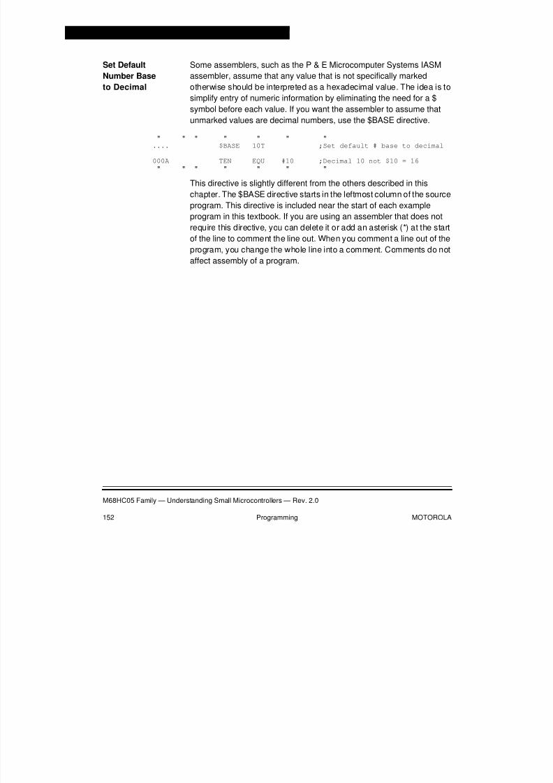
8/2/2019 122 Textbook
http://slidepdf.com/reader/full/122-textbook 152/331
Programming
M68HC05 Family — Understanding Small Microcontrollers — Rev. 2.0
152 Programming MOTOROLA
Set Default
Number Base
to Decimal
Some assemblers, such as the P & E Microcomputer Systems IASM
assembler, assume that any value that is not specifically marked
otherwise should be interpreted as a hexadecimal value. The idea is to
simplify entry of numeric information by eliminating the need for a $
symbol before each value. If you want the assembler to assume that
unmarked values are decimal numbers, use the $BASE directive.
" " " " " " "
.... $BASE 10T ;Set default # base to decimal
000A TEN EQU #10 ;Decimal 10 not $10 = 16
" " " " " " "
This directive is slightly different from the others described in this
chapter. The $BASE directive starts in the leftmost column of the source
program. This directive is included near the start of each example
program in this textbook. If you are using an assembler that does not
require this directive, you can delete it or add an asterisk (*) at the start
of the line to comment the line out. When you comment a line out of the
program, you change the whole line into a comment. Comments do not
affect assembly of a program.

8/2/2019 122 Textbook
http://slidepdf.com/reader/full/122-textbook 153/331
Programming
Instruction Set Dexterity
M68HC05 Family — Understanding Small Microcontrollers — Rev. 2.0
MOTOROLA Programming 153
Instruction Set Dexterity
As in most engineering fields, more than one sequence of instructions
can perform any task. A good way to learn a new instruction set is to seehow many different ways you can solve some small programming
problem. This is called instruction set dexterity.
Figure 36 shows four different ways to check for closure of a switch
connected to port A bit 0. Two of these ways were used in the example
program of Listing 3. Assembler Listing. Although all of the sequences
accomplish the same basic task, there are subtle differences. Usually
these differences are not significant, but sometimes they can save
execution time or program memory space. In a small microcontroller,
memory space can be an important consideration.
0000 PORTA EQU $00 ;Direct address of port A
0300 ORG $0300 ;Program will start at $0300
0300 B6 00 [ 3] TOP1 LDA PORTA ;Read sw at LSB of Port A
0302 A4 01 [ 2] AND #$01 ;To test bit-0
0304 27 FA [ 3] BEQ TOP1 ;Loop till bit-0 = 1
0306 01 00 FD [ 5] TOP2 BRCLR 0,PORTA,TOP2 ;Loop here till sw ON
0309 B6 00 [ 3] TOP3 LDA PORTA ;Read sw at LSB of Port A
030B 44 [ 3] LSRA ;Bit-0 shifts to carry
030C 24 FB [ 3] BCC TOP3 ;Loop till switch ON
030E A6 01 [ 2] LDA #$01 ;1 in LSB
0310 B5 00 [ 3] TOP4 BIT PORTA ;To test sw at bit-0
0312 27 FC [ 3] BEQ TOP4 ;Loop till switch ON
Figure 36. Four Ways to Check a Switch
The numbers in square brackets are the number of CPU cycles required
for the instruction on that line of the program. The TOP1 sequence takes
six bytes of program space and eight cycles. The accumulator is $01
when the program falls through the BEQ statement. The TOP2sequence takes only three bytes and five cycles, and the accumulator is
not disturbed. (This is probably the best sequence in most cases.) The
TOP3 sequence takes one less byte than the TOP1 sequence but also
takes one extra cycle to execute. After the TOP3 sequence, the
accumulator still holds the other seven bits from the port A read,
8/2/2019 122 Textbook
http://slidepdf.com/reader/full/122-textbook 154/331
Programming
M68HC05 Family — Understanding Small Microcontrollers — Rev. 2.0
154 Programming MOTOROLA
although they have been shifted one position to the right. The last
sequence takes six bytes and a total of eight cycles, but the loop itself is
only six cycles. By working through exercises like this, you will improve
your instruction set dexterity. This will be very helpful when you need to
reduce a program by a few bytes to fit it into the available memory space.
Application Development
A simple development system for the MC68HC705J1A is offered by
Motorola (M68HC705JICS). This system includes an in-circuit simulator
(software and hardware circuit board). The circuit board plugs into a
serial (com) port on a personal computer. A connector and cable allow
the in-circuit simulator to be plugged into an application system to takethe place of the microcontroller that will eventually be used. A socket is
also provided that allows an EPROM or OTP version of the
MC68HC705J1A to be programmed from the personal computer.
A simulator is a program for a personal computer that helps during
program development and debugging. This tool simulates the actions of
a real microcontroller but has some important advantages. For instance,
in a simulator, you have complete control over when and if the simulated
CPU should advance to the next instruction. You can also look at and
change registers or memory locations before going to the next
instruction.
Simulators do not run at real-time speed. Since the personal computer
is simulating MCU actions with software programs, each MCU
instruction takes much longer to execute than it would in a real MCU. For
many MCU programs, this speed reduction is not noticeable. As slow as
a simulator can be, it is still very fast in human terms. Some MCU
programs generate time delays with software loops (like the DLY50
routine in Listing 3. Assembler Listing). The 50-millisecond delay of
DLY50 might take tens of seconds on some personal computers. To
make the simulation run faster, you can temporarily replace the loop
count value (65) with a much smaller number (for instance, 2).
NOTE: Remember to put the original number back before programming the
finished program into the EPROM of a real MCU.

8/2/2019 122 Textbook
http://slidepdf.com/reader/full/122-textbook 155/331
Programming
Application Development
M68HC05 Family — Understanding Small Microcontrollers — Rev. 2.0
MOTOROLA Programming 155
An in-circuit simulator is a simulator that can be connected to a user
system in place of the microcontroller. An ordinary simulator normally
only takes input information from the personal computer and displays
outputs and results on the personal computer display. An in-circuit
simulator goes beyond this to emulate the input and output interfaces of
the real microcontroller.
Program development is easier with a simulator than a real MCU. It is
easier to make program changes and try them out in the simulator than
to program an EPROM device and try it out. With the real MCU, you can
only see the input and output pins, and you cannot easily stop a program
between instructions. But with the simulator, you can execute a single
instruction at a time and look at registers and memory contents at every
step. This makes it easier to see which instructions failed to perform as
intended. A simulator can also inform you if the program attempts to use
the value of a variable before it has been initialized.
An in-circuit emulator is a real-time development tool. The emulator is
built around an actual MCU, so it can execute program instructions
exactly as they will be executed in the finished application. An emulator
has RAM memory where the ROM or EPROM memory will be located in
the finalMCU. This allows you to load programs quickly into the emulator
and to change these programs during development.
Extra circuitry in the emulator allows you to set breakpoints in theprogram under development. When the program reaches one of these
breakpoint addresses, the program under development is temporarily
stopped and a development monitor program takes control. This
monitor program allows you to look at or change CPU registers, memory
locations, or control registers. An emulator typically has less visibility of
internal MCU actions than a simulator, but it can run at full real-time
speed. An emulator cannot normally stop clocks to internal peripheral
systems like a timer, when control switches from the application program
to the monitor program. A simulator can stop such clocks.

8/2/2019 122 Textbook
http://slidepdf.com/reader/full/122-textbook 156/331
Programming
M68HC05 Family — Understanding Small Microcontrollers — Rev. 2.0
156 Programming MOTOROLA
Review
The process of writing a program begins with a plan. A flowchart can be
used to document the plan. Mnemonic source code statements are thenwritten for each block of the flowchart. Mnemonic source code
statements can include any of the instructions from the instruction set of
the microcontroller. The next step is to combine all of the program
instructions with assembler directives to get a text source file.
Assembler directives are program statements that give instructions to
the assembler rather than to the CPU. These instructions tell the
assembler things like where to locate instructions in the memory of the
microcontroller. Assembler directives can also inform the assembler of
the binary meaning of a mnemonic label. Six directives were discussed.
• ORG — Originate directives set the starting address for the object
code that follows.
• EQU — Equate directives associate a label with a binary number
or address.
• FCB — Form constant byte directives are used to introduce 8-bit
constant data values into a program.
• FDB — Form double byte directives are used to introduce 16-bit
data or address constants into a program.
• RMB — Reserve memory byte(s) directives are used to assign
labels (belonging to program variables) to RAM addresses.
• $BASE 10T — Change default number base to decimal.
After the complete source program is written, it is processed by an
assembler to produce a listing file and an S-record object file. The listing
file is part of the documentation of the program. The S-record object file
can be loaded into the simulator or it can be programmed into a
microcontroller.
A conditional loop can produce a timed delay. The delay is dependent
on the execution time of the instructions in the loop. A subroutine such
as this delay routine can be used many times in a program by calling it
with JSR or BSR instructions.

8/2/2019 122 Textbook
http://slidepdf.com/reader/full/122-textbook 157/331
Programming
Review
M68HC05 Family — Understanding Small Microcontrollers — Rev. 2.0
MOTOROLA Programming 157
Instruction set dexterity is the ability to solve a programming problem in
several different ways with different sequences of instructions. Since
each sequence takes a different number of program bytes and a
different number of CPU cycles to execute, you can select a sequence
that is best for each situation.
A simulator is an application development tool that runs on a personal
computer and simulates the behavior of a microcontroller (though not at
real-time speed). An in-circuit simulator takes this idea further to also
simulate the I/O interfaces of the microcontroller. The in-circuit simulator
can be plugged into an application circuit in place of the microcontroller.
A simulator makes application development easier. It allows instructions
to be executed one at a time. It also provides visibility into the contents
of registers and memory and allows changes before executing a new
instruction.
An emulator is built around a real MCU so it can run at the full speed of
the final MCU. Emulators use RAM instead of ROM or EPROM so the
program under development can be modified easily during
development.

8/2/2019 122 Textbook
http://slidepdf.com/reader/full/122-textbook 158/331
Programming
M68HC05 Family — Understanding Small Microcontrollers — Rev. 2.0
158 Programming MOTOROLA

8/2/2019 122 Textbook
http://slidepdf.com/reader/full/122-textbook 159/331
M68HC05 Family — Understanding Small Microcontrollers — Rev. 2.0
MOTOROLA The Paced Loop 159
The Paced Loop
Contents
Introduction . . . . . . . . . . . . . . . . . . . . . . . . . . . . . . . . . . . . . . . . . . . .159
System Equates . . . . . . . . . . . . . . . . . . . . . . . . . . . . . . . . . . . . . . . .160
Register Equates for MC68HC705J1A . . . . . . . . . . . . . . . . . . . . .160
Application System Equates . . . . . . . . . . . . . . . . . . . . . . . . . . . . .161
Vector Setup . . . . . . . . . . . . . . . . . . . . . . . . . . . . . . . . . . . . . . . . . . .162Reset Vector . . . . . . . . . . . . . . . . . . . . . . . . . . . . . . . . . . . . . . . . .162
Unused Interrupts . . . . . . . . . . . . . . . . . . . . . . . . . . . . . . . . . . . . .163
RAM Variables. . . . . . . . . . . . . . . . . . . . . . . . . . . . . . . . . . . . . . . . . .165
Paced Loop . . . . . . . . . . . . . . . . . . . . . . . . . . . . . . . . . . . . . . . . . . . .165
Loop Trigger . . . . . . . . . . . . . . . . . . . . . . . . . . . . . . . . . . . . . . . . .167
Loop System Clock . . . . . . . . . . . . . . . . . . . . . . . . . . . . . . . . . . . .168
Your Programs . . . . . . . . . . . . . . . . . . . . . . . . . . . . . . . . . . . . . . .168
Timing Considerations . . . . . . . . . . . . . . . . . . . . . . . . . . . . . . . . .169
Stack Considerations . . . . . . . . . . . . . . . . . . . . . . . . . . . . . . . . . .170An Application-Ready Framework. . . . . . . . . . . . . . . . . . . . . . . . . . .171
Review. . . . . . . . . . . . . . . . . . . . . . . . . . . . . . . . . . . . . . . . . . . . . . . .178
Introduction
This chapter presents a general-purpose software structure that may be
used as a framework for many microcontroller applications. Major
system tasks are written as subroutines. These subroutines areorganized into a loop so that each is called once per pass through the
loop. At the top of the loop there is a short routine that paces the loop so
that it is executed at regular intervals. A software clock is maintained as
the first task in the loop. This clock can be used as an input to the other

8/2/2019 122 Textbook
http://slidepdf.com/reader/full/122-textbook 160/331
The Paced Loop
M68HC05 Family — Understanding Small Microcontrollers — Rev. 2.0
160 The Paced Loop MOTOROLA
task subroutines to decide what the routine should do on each pass
through the major loop.
In addition to the loop structure itself, this chapter discusses system
initialization issues and software setup details so you can go directly tothe routines that deal with your specific applications.
System Equates
Because using binary bit patterns and addresses in programs
instructions is inconvenient, equate (EQU) directives are used to assign
mnemonic names to register addresses and bit positions. These names
can then be used in program instructions instead of the binary numbers.This makes the program easier to write and to read. When an in-circuit
simulator is used to develop an application program, the mnemonic
names can be used in the debug displays instead of the binary
addresses.
Register
Equates for
MC68HC705J1A
The manufacturer’s recommended names for registers and control bits
are included in the paced loop program framework of Listing 4. Paced
Loop Framework Program in this chapter. This allows you to write
program instructions using names that make sense to people instead ofobscure binary numbers and addresses.
Each register is equated to its direct-page binary address with an EQU
directive. Each control bit is defined in two ways:
• First, an EQU directive equates the bit name to a number between
7 and 0 corresponding to the bit number where each bit is located
in a control register.
• Second, most control bits are equated to a binary bit pattern such
as 0010 0000 ($20) which can be used as a bit mask to identify thelocation of the bit in a register.
Since you cannot equate the same name to two different binary values,
the second equate uses a period after the bit name. To get a bit name’s
bit number (7–0), use the name; to get a mask indicating the bit position,

8/2/2019 122 Textbook
http://slidepdf.com/reader/full/122-textbook 161/331
The Paced Loop
System Equates
M68HC05 Family — Understanding Small Microcontrollers — Rev. 2.0
MOTOROLA The Paced Loop 161
use the name followed by a period. This convention is used in the paced
loop framework, but it is not necessarily a standard that is recommended
by Motorola or the assembler companies.
In the M68HC05 instruction set, the bit manipulation instructions are ofthe form
xxxx 14 08 ----- BSET bit#,dd ;Set bit in location dd
Bit# is a number between 7 and 0 that identifies the bit within the register
at location dd that is to be changed or tested.
In other cases, you may want to build up a mask with several bits set,
and then write this composite value to a register location. For example,
suppose you want to set RTIFR, RTIE, and RT1 bits in the TSCR
register. You could use these instructions.
xxxx A6 16 LDA #RTIFR.+RTIE.+RT1.;Form mask
xxxx B7 08 STA TSCR ;Write mask to TSCR register
The # symbol means immediate addressing mode. The expression
(RTIFR.+RTIE.+RT1.) is the Boolean OR of three bit position masks.
The assembler evaluates the Boolean expression during program
assembly andsubstitutes the answer (a single 8-bit binary value) into the
assembled program. These program statements would produce exactly
the same results, but they are not as easy to read.
xxxx A6 16 LDA #%00010110 ;Form mask
xxxx B7 08 STA $08 ;Write mask to TSCR register
Application
System Equates
Usually, some application-specific equate directives will be in a program
to define the signals connected to I/O pins. These EQU directives should
be placed after the standard MCU equate directives and before the main
program starts. The paced loop framework program was developed with
a particular small development PC board in mind. This system has a
switch connected to port A bit 0 and an LED connected to port A bit 7,
so these connections were defined with EQU directives.
The switch is not used in the paced loop framework program of
Listing 4. Paced Loop Framework Program, but it does no harm to
include the related EQU directives. EQU directives do not generate any
object code that takes up memory space in the final computer system.

8/2/2019 122 Textbook
http://slidepdf.com/reader/full/122-textbook 162/331
The Paced Loop
M68HC05 Family — Understanding Small Microcontrollers — Rev. 2.0
162 The Paced Loop MOTOROLA
Vector Setup
All MCU programs should set up the reset and interrupt vectors.
Vectors specify the address where the CPU will start processing
instructions when a reset or interrupt occurs. Reset and each interrupt
source expect to find their associated vector in a specific pair of memory
locations. For example, the reset vector is at the highest two locations in
memory ($07FE and $07FF in the MC68HC705J1A). If you do not place
values in these locations, the CPU will take whatever binary values it
finds there and treat them as if they were a 2-byte address you stored
there.
Reset Vector The usual way to define a vector is with an FDB directive.
07FE 03 00 RESETV FDB START ;Beginning of program on reset
During assembly, the assembler evaluates the label START into a
2-byte address and stores this address in the next two available memory
locations of the program. The columns at the left of the listing line show
that the address $0300 was stored at $07FE and $07FF ($03 at $07FE
and $00 at $07FF).
RESETV is an optional label on this program line. Although it is not usedfor reference by other statements in this particular program, it was
included to identify this FDB directive line as the statement that defines
the reset vector.
The reset vector was set up to point at the label START. The in-circuit
simulator system that Motorola offers as a low-cost development tool
uses this information to set up the simulator screen. When a program is
loaded into the simulator, the simulator looks for the address in the reset
vector of the loaded program. If one is found, the simulator selects that
program instruction and displays it in the source program window of thesimulator. The simulator’s PC is also set to this address. If there is no
reset vector, the simulator displays a warning message, saying that the
reset vector was not initialized. You could still debug the program, but it
would not work if it was programmed into an EPROM MCU because the
program would not start at reset.

8/2/2019 122 Textbook
http://slidepdf.com/reader/full/122-textbook 163/331
The Paced Loop
Vector Setup
M68HC05 Family — Understanding Small Microcontrollers — Rev. 2.0
MOTOROLA The Paced Loop 163
Unused Interrupts For interrupts that are used, the vectors can be defined just as the reset
vector was defined (with an FDB directive). In the paced loop framework
program, the timer interrupt is used for real-time interrupts (RTI). The
external interrupt and the SWI (software interrupt) are not used.
It is a good idea to set up the unused interrupt vectors just in case one
of these interrupts is requested unexpectedly. This is not to say that
unexpected interrupts can occur in a working computer system. Rather,
it says that when a programmer is first starting out, programming
mistakes could result in unintended interrupt sources being enabled and
triggered.
This listing shows how interrupt and reset vectors were set up in the
paced loop framework program.
*******************************************************
* RTIF interrupt service routine
*******************************************************
0345 3A E0 RTICNT DEC RTIFs ;On each RTIF
" " " " " " "
" " " " " " "
0351 80 AnRTI RTI ;Return from RTIF interrupt
0351 UNUSED EQU AnRTI ;Use RTI at AnRTI for unused
;interrupts to just return
*******************************************************
* Interrupt & reset vectors*******************************************************
07F8 ORG $07F8 ;Start of vector area
07F8 03 45 TIMVEC FDB RTICNT ;Count RTIFs 3/TIC
07FA 03 51 IRQVEC FDB UNUSED ;Change if vector used
07FC 03 51 SWIVEC FDB UNUSED ;Change if vector used
07FE 03 00 RESETV FDB START ;Beginning of program on reset
The first lines in this partial listing show the first and last lines of the timer
interrupt service routine. The line
0351 80 AnRTI RTI ;Return from RTIF interrupt
shows a return-from-interrupt (RTI) instruction with the label AnRTI. The
next line equates the label UNUSED to the address of the RTI instruction
at AnRTI. Further down in the listing, the unused interrupt vectors for
external interrupts and SWI interrupts are set up to point at this RTI
instruction. During assembly, the assembler encounters the label

8/2/2019 122 Textbook
http://slidepdf.com/reader/full/122-textbook 164/331
The Paced Loop
M68HC05 Family — Understanding Small Microcontrollers — Rev. 2.0
164 The Paced Loop MOTOROLA
UNUSED and finds it should be equal to AnRTI that is in turn equal to
the binary address of the RTI instruction ($0351).
If an SWI interrupt were unexpectedly encountered, the CPU would save
the CPU registers on the stack (temporary RAM) and load the programcounter with the address $0351 from the SWI vector. The CPU would
then load the instruction RTI from address $0351. The RTI instruction
would tell the CPU to recover the saved CPU registers (including the
program counter) from the stack. The recovered program counter value
would determine what the CPU did next.
An alternate way to respond to unexpected interrupts would be to reset
the stack pointer (with an RSP instruction) and then jump to the same
address as if a resethad occurred. This approach makes the pessimistic
assumption that if an unexpected interrupt occurs, there may be otherserious problems. By resetting the stack pointer and starting all over you
are more likely to correct whatever caused the unexpected interrupt.
While debugging a program on a simulator, there is another possible
way to handle unused interrupts.
" " " " " " "
0351 BADINT BRA BADINT ;Infinite loop to here
" " " " " " "
" " " " " " "
07FA 03 51 VECTOR FDB BADINT ;Hang on unexpected int" " " " " " "
In this scheme, an unexpected interrupt will cause the CPU to vector to
BADINT. The instruction at BADINT is an infinite loop back to BADINT,
so the system will hang there. You can stop the simulator and check the
CPU register values on the stack to see what the program was doing
when it got the unexpected interrupt.
8/2/2019 122 Textbook
http://slidepdf.com/reader/full/122-textbook 165/331
The Paced Loop
RAM Variables
M68HC05 Family — Understanding Small Microcontrollers — Rev. 2.0
MOTOROLA The Paced Loop 165
RAM Variables
Program variables change value during the course of executing the
program. Thesevalues cannot be specified before the program is writtenand programmed into the MCU. The CPU must use program instructions
to initialize and modify these values. When the program is written, space
is reserved for variables in the RAM memory of the MCU, using reserve
memory byte(s) (RMB) directives.
First, you would put an originate (ORG) directive to set the assembler’s
location counter to the address of the start of RAM in the MCU ($00C0
in the MC68HC705J1A). Each variable or group of variables would be
set up with an RMB directive. The RMB line is identified by the name of
the variable. The assembler assigns the name (label) to the nextavailable address. After each new variable or group of variables is
assigned, the location counter is advanced to point at the next free
memory location.
As the program in Listing 4. Paced Loop Framework Program shows,
some programmers feel it is good practice to clear all RAM locations as
one of the first initialization steps after any reset. While you are
debugging a system, it is useful to have a known set of starting
conditions. If the entire RAM is cleared at the start of a program, it is easy
to tell if any locations have been written.
Paced Loop
The paced loop is a general-purpose software structure that is suitable
for a wide variety of MCU applications. The main idea is to break the
overall application into a series of tasks such as keeping track of time,
reading system inputs, and updating system outputs. Each task is
written as a subroutine. A main loop is constructed out of jump-to-subroutine (JSR) instructions for each task. At the top of the
loop is a software pacemaker. When the pacemaker triggers, the list of
task subroutines is executed once and a branch instruction takes you to
the top of the loop to wait for the next pacemaker trigger.

8/2/2019 122 Textbook
http://slidepdf.com/reader/full/122-textbook 166/331
The Paced Loop
M68HC05 Family — Understanding Small Microcontrollers — Rev. 2.0
166 The Paced Loop MOTOROLA
Figure 37 shows a flowchart for the main paced loop. The top block is a
loop that waits for the pacemaker trigger (every 100 milliseconds). The
next few blocks have to do with maintaining the TIC counter. The version
of this program in Listing 4. Paced Loop Framework Program has two
simple main tasks, TIME and BLINK. You would remove one or both of
these routines and substitute your own tasks. The only limitation on the
number of main tasks is that they must all finish quickly enough so no
pacemaker triggers are lost. The last block in the flowchart is just a
branch back to the top of the loop to wait for the next pacemaker trigger.
Figure 37. Flowchart of Main Paced Loop
MAINPACED LOOP
TIC = 10 ?
YES
NO
CLEAR MSB OF TIC
CALL TASK ROUTINE TIME
MAIN
ARNC1
MSB OF TIC = 1 ?
YES
NO
TIC = TIC + 1
SET TIC = 0
CALL TASK ROUTINE BLINK
INSERT
TASK ROUTINES
HERE

8/2/2019 122 Textbook
http://slidepdf.com/reader/full/122-textbook 167/331
The Paced Loop
Paced Loop
M68HC05 Family — Understanding Small Microcontrollers — Rev. 2.0
MOTOROLA The Paced Loop 167
Loop Trigge r In the paced loop program of Listing 4. Paced Loop Framework
Program, the pacemaker is based on the on-chip real-time interrupt
(RTI). This RTI is set to generate an interrupt to the CPU every 32.8
milliseconds. The flowchart in Figure 37 shows what happens at each
RTI. This interrupt activity can be thought of as if it were taking place
asynchronously with respect to the main program. The most significant
bit of the TIC variable is used as a flag to tell the main program when it
is time to increment TIC and execute one pass through the paced loop.
Figure 38. Flowchart of RTI Service Routine
The RAM variable RTIFs is used to count three real-time interrupts
before setting the MSB of TIC. The main program will be watching TIC
to see when the MSB becomes set.
Every 32.8 ms the RTIF flag will get set, triggering a timer interrupt
request. One of the duties of an interrupt service routine is to clear the
flag that caused the interrupt before returning from the interrupt. If RTIF
BEGIN RTIFINTERRUPT ROUTINE
RTIFs = 0 ?
YES
NO
RETURN FROM
INTERRUPT
RTIFs = RTIFs – 1
RTIFs = 3
CLEAR RTIF INTERRUPT FLAG
RTICNT
SET MSB OF TIC
ENDRTI
AnRTI

8/2/2019 122 Textbook
http://slidepdf.com/reader/full/122-textbook 168/331
The Paced Loop
M68HC05 Family — Understanding Small Microcontrollers — Rev. 2.0
168 The Paced Loop MOTOROLA
is not cleared before the return, a new interrupt request is generated
immediately instead of waiting for the 32.8-ms trigger.
Loop SystemClock
The variable TIC is the most basic clock for the pacemaker. TIC countsfrom 0 to 10. As TIC is incremented from 9 to 10, the program recognizes
this and resets TIC to 0. Except within the pacemaker itself, TIC appears
to count from 0 to 9. TIC is equal to 0 on every tenth trigger of the
pacemaker.
The first task subroutine in the main loop is called TIME. This routine
maintains a slower clock called TOC. TOC is incremented each time the
paced loop executes and TIC is 0 (every tenth pass through the paced
loop). TOC is set up as a software counter that counts from 0 through
59. The remaining task routines after TIME can use the current valuesof TIC and TOC to decide what needs to be done on this pass through
the paced loop.
In Listing 4. Paced Loop Framework Program, the pace is keyed to
the RTI which does not happen to be an integer submultiple of one
second. Three RTI periods equal 98.4 milliseconds. This is pretty close
to 0.1 second but not close enough to be used like a wristwatch. You
could get accurate real time if you modified the paced loop program to
use a different trigger source such as zero crossings of the ac
(alternating current) line (60 Hz). Although the ac line is not as accurateas a crystal over short periods of time, it is very accurate over long
periods. Most clocks that plug into the wall use the ac line timing as the
basis for keeping time.
Your Programs The task subroutines have few restrictions. Each task subroutine should
do everything it needs to do, as quickly as it can, and then execute a
return from subroutine (RTS). The total time required to execute one
pass through all of the task subroutines must be less than two
pacemaker triggers. (We will explain this in greater detail.) The important
point is that a task subroutine should not wait for the occurrence of some
external event like a switch to be pressed. This would defeat the
timekeeping aspects of the paced loop.

8/2/2019 122 Textbook
http://slidepdf.com/reader/full/122-textbook 169/331
The Paced Loop
Paced Loop
M68HC05 Family — Understanding Small Microcontrollers — Rev. 2.0
MOTOROLA The Paced Loop 169
The paced loop can automatically provide for switch debouncing.
Switches are notorious for bouncing between the closed and opened
conditions as they are pressed and released. It is not at all unusual for a
switch to bounce for 50 milliseconds or more as it is pressed. A
microcontroller can execute instructions so fast that a single press of a
switch might look like several presses to a program, unless steps are
taken to account for switch bounce. There are hardware methods for
debouncing switches but they require extra components and increase
the cost of a product.
Software can also be used to debounce a switch. The example program
in Figure 31. Flowchart and Mnemonics used a simple software delay
program to debounce a switch, but this routine should not be used
directly in the paced loop structure because it takes too much time. In a
paced loop, you can debounce a switch by reading it on consecutive
passes through the paced loop. The first time you see the switch
pressed, you can write a special value to a variable to indicate that a
switch was tentatively pressed. (You would not consider this switch as
pressed yet.) On the next pass through the paced loop, you would either
mark the switch as really pressed or clear the mark to indicate that it was
a false detection. Similarly, when the switch is eventually released, you
can mark it as tentatively released and on the next pass mark it as really
released.
Timing
Considerations
Ideally, you should finish all of the task subroutines in the paced loop
before the next pacemaker trigger arrives. If a single pass through the
loop takes longer than the pacemaker trigger period, the flag that
indicates it is time to start the next pass through the main loop will
already be set when you get back to the top of the loop. Nothing bad
happens unless you get so far behind that a new pacemaker trigger
comes before the previous one has been recognized. The paced loop
remains valid unless any two consecutive passes take more than two
pacemaker trigger periods.
A little bit of planning can ensure that no two consecutive passes through
the loop take longer than two pacemaker periods. Especially long task
subroutines can be scheduled to execute during a particular paced loop
pass when very little other activity is scheduled. A simple check of one

8/2/2019 122 Textbook
http://slidepdf.com/reader/full/122-textbook 170/331
The Paced Loop
M68HC05 Family — Understanding Small Microcontrollers — Rev. 2.0
170 The Paced Loop MOTOROLA
of the time variables such as TIC or TOC can be used to decide whether
or not to perform a particularly slow routine. If there were several things
that needed to be done once per second, one could be scheduled for the
TIC = 0 pass, another could be scheduled for the TIC = 2 pass, and so
on.
Stack
Considerations
Small microcontrollers like the MC68HC705J1A have only small
amounts of RAM for the stack and program variables. Interrupts take five
bytes of stack RAM and each subroutine call takes two bytes on the
stack. If a subroutine called another subroutine and an interrupt was
requested before the second subroutine was finished, the stack would
use 2+2+5 = 9 RAM bytes of the available 64. If the stack gets too deep,
there is a danger that RAM variables can get written over with stack data.
To avoid these problems, you should calculate the worst case depth that
your stack can ever get to. In the MC68HC705J1A, the sum of all system
variables plus the worst case stack depth must be less than or equal to
the 64 available RAM locations.
Fortunately, an interrupt causes the interrupt mask (I) bit in the condition
code register to be set in response to any interrupt. This blocks
additional interrupts until the I bit is cleared (normally upon return from
the interrupt).

8/2/2019 122 Textbook
http://slidepdf.com/reader/full/122-textbook 171/331
The Paced Loop
An Application-Ready Framework
M68HC05 Family — Understanding Small Microcontrollers — Rev. 2.0
MOTOROLA The Paced Loop 171
An Application-Ready Framework
The paced loop program of Listing 4. Paced Loop Framework
Program can be used as the basis for your own applications. Thisframework provides these main parts:
• Equate statements for all MC68HC705J1A register and bit names
• Application-specific equate statements
• Program variables section
• Initialization section (START)
• Pacemaker for main loop based on RTI
• Calls to task subroutines
• Two simple examples of task subroutines (TIME and BLINK)
• An interrupt service routine for RTIF interrupts
• Vector definition section
The pacemaker in this particular paced loop program triggers a pass
through the main loop about once every 100 milliseconds (actually 98.4
ms). This can be changed easily to some other number of real-time
interrupts and the RTI rate can be changed. For applications that need
real wristwatch time, the pacemaker can be modified to work from
interrupts generated at zero crossings of the ac power line.Additional RMB directives should be added to the program variables
section. Additional EQU statements can be added just above the
program variables section to add application-specific equates.
In its present form, the paced loop has only two simple task subroutines
(TIME and BLINK). The TIME task just maintains a 0 to 59 count (TOC)
which could be useful for measuring or generating longer time periods.
The BLINK task is just a dummy routine to demonstrate how a task can
use the time variable TOC to control a system action. In this case, the
action is to turn on an LED when TOC is even, and turn it off when TOC
is odd. To use the framework program for your own application, you
should remove the BLINK task and replace it with your own tasks.
The RTI service routine serves as an example of an interrupt handler
and counts real-time interrupts to set the pacemaker rate.

8/2/2019 122 Textbook
http://slidepdf.com/reader/full/122-textbook 172/331
The Paced Loop
M68HC05 Family — Understanding Small Microcontrollers — Rev. 2.0
172 The Paced Loop MOTOROLA
Listing4. PacedLoop Framework Program
Listing 4. Paced Loop Framework Program (Sheet 1 of 6)
$BASE 10T******************************************************** Equates for MC68HC705J1A MCU
* Use bit names without a dot in BSET..BRCLR* Use bit name preceded by a dot in expressions such as* #.ELAT+.EPGM to form a bit mask*******************************************************PORTA EQU $00 ;I/O port APA7 EQU 7 ;Bit #7 of port APA6 EQU 6 ;Bit #6 of port APA5 EQU 5 ;Bit #5 of port APA4 EQU 4 ;Bit #4 of port APA3 EQU 3 ;Bit #3 of port APA2 EQU 2 ;Bit #2 of port APA1 EQU 1 ;Bit #1 of port APA0 EQU 0 ;Bit #0 of port APA7. EQU $80 ;Bit position PA7PA6. EQU $40 ;Bit position PA6PA5. EQU $20 ;Bit position PA5PA4. EQU $10 ;Bit position PA4PA3. EQU $08 ;Bit position PA3PA2. EQU $04 ;Bit position PA2PA1. EQU $02 ;Bit position PA1PA0. EQU $01 ;Bit position PA0
PORTB EQU $01 ;I/O port BPB5 EQU 5 ;Bit #5 of port BPB4 EQU 4 ;Bit #4 of port BPB3 EQU 3 ;Bit #3 of port BPB2 EQU 2 ;Bit #2 of port BPB1 EQU 1 ;Bit #1 of port BPB0 EQU 0 ;Bit #0 of port B
PB5. EQU $20 ;Bit position PB5PB4. EQU $10 ;Bit position PB4PB3. EQU $08 ;Bit position PB3PB2. EQU $04 ;Bit position PB2PB1. EQU $02 ;Bit position PB1PB0. EQU $01 ;Bit position PB0
DDRA EQU $04 ;Data direction for port ADDRA7 EQU 7 ;Bit #7 of port A DDRDDRA6 EQU 6 ;Bit #6 of port A DDRDDRA5 EQU 5 ;Bit #5 of port A DDRDDRA4 EQU 4 ;Bit #4 of port A DDRDDRA3 EQU 3 ;Bit #3 of port A DDRDDRA2 EQU 2 ;Bit #2 of port A DDRDDRA1 EQU 1 ;Bit #1 of port A DDRDDRA0 EQU 0 ;Bit #0 of port A DDRDDRA7. EQU $80 ;Bit position DDRA7DDRA6. EQU $40 ;Bit position DDRA6DDRA5. EQU $20 ;Bit position DDRA5DDRA4. EQU $10 ;Bit position DDRA4DDRA3. EQU $08 ;Bit position DDRA3DDRA2. EQU $04 ;Bit position DDRA2

8/2/2019 122 Textbook
http://slidepdf.com/reader/full/122-textbook 173/331
The Paced Loop
An Application-Ready Framework
M68HC05 Family — Understanding Small Microcontrollers — Rev. 2.0
MOTOROLA The Paced Loop 173
Listing 4. Paced Loop Framework Program (Sheet 2 of 6)
DDRA1. EQU $02 ;Bit position DDRA1DDRA0. EQU $01 ;Bit position DDRA0
DDRB EQU $05 ;Data direction for port BDDRB5 EQU 5 ;Bit #5 of port B DDRDDRB4 EQU 4 ;Bit #4 of port B DDRDDRB3 EQU 3 ;Bit #3 of port B DDRDDRB2 EQU 2 ;Bit #2 of port B DDRDDRB1 EQU 1 ;Bit #1 of port B DDRDDRB0 EQU 0 ;Bit #0 of port B DDRDDRB5. EQU $20 ;Bit position DDRB5DDRB4. EQU $10 ;Bit position DDRB4DDRB3. EQU $08 ;Bit position DDRB3DDRB2. EQU $04 ;Bit position DDRB2DDRB1. EQU $02 ;Bit position DDRB1DDRB0. EQU $01 ;Bit position DDRB0
TSCR EQU $08 ;Timer status & control reg
TOF EQU 7 ;Timer overflow flagRTIF EQU 6 ;Real time interrupt flagTOIE EQU 5 ;TOF interrupt enableRTIE EQU 4 ;RTI interrupt enableTOFR EQU 3 ;TOF flag resetRTIFR EQU 2 ;RTIF flag resetRT1 EQU 1 ;RTI rate select bit 1RT0 EQU 0 ;RTI rate select bit 0TOF. EQU $80 ;Bit position TOFRTIF. EQU $40 ;Bit position RTIFTOIE. EQU $20 ;Bit position TOIERTIE. EQU $10 ;Bit position RTIETOFR. EQU $08 ;Bit position TOFRRTIFR. EQU $04 ;Bit position RTIFR
RT1. EQU $02 ;Bit position RT1RT0. EQU $01 ;Bit position RT0
TCR EQU $09 ;Timer counter register
ISCR EQU $0A ;IRQ status & control regIRQE EQU 7 ;IRQ edge/edge-levelIRQF EQU 3 ;External interrupt flagIRQR EQU 1 ;IRQF flag reset
PDRA EQU $10 ;Pulldown register for port APDIA7 EQU 7 ;Pulldown inhibit for PA7PDIA6 EQU 6 ;Pulldown inhibit for PA6PDIA5 EQU 5 ;Pulldown inhibit for PA5PDIA4 EQU 4 ;Pulldown inhibit for PA4
PDIA3 EQU 3 ;Pulldown inhibit for PA3PDIA2 EQU 2 ;Pulldown inhibit for PA2PDIA1 EQU 1 ;Pulldown inhibit for PA1PDIA0 EQU 0 ;Pulldown inhibit for PA0PDIA7. EQU $80 ;Bit position PDIA7PDIA6. EQU $40 ;Bit position PDIA6PDIA5. EQU $20 ;Bit position PDIA5

8/2/2019 122 Textbook
http://slidepdf.com/reader/full/122-textbook 174/331
The Paced Loop
M68HC05 Family — Understanding Small Microcontrollers — Rev. 2.0
174 The Paced Loop MOTOROLA
Listing 4. Paced Loop Framework Program (Sheet 3 of 6)
PDIA4. EQU $10 ;Bit position PDIA4
PDIA3. EQU $08 ;Bit position PDIA3
PDIA2. EQU $04 ;Bit position PDIA2
PDIA1. EQU $02 ;Bit position PDIA1PDIA0. EQU $01 ;Bit position PDIA0
PDRB EQU $11 ;Pulldown register for port B
PDIB5 EQU 5 ;Pulldown inhibit for PB5
PDIB4 EQU 4 ;Pulldown inhibit for PB4
PDIB3 EQU 3 ;Pulldown inhibit for PB3
PDIB2 EQU 2 ;Pulldown inhibit for PB2
PDIB1 EQU 1 ;Pulldown inhibit for PB1
PDIB0 EQU 0 ;Pulldown inhibit for PB0
PDIB5. EQU $20 ;Bit position PDIB5
PDIB4. EQU $10 ;Bit position PDIB4
PDIB3. EQU $08 ;Bit position PDIB3
PDIB2. EQU $04 ;Bit position PDIB2
PDIB1. EQU $02 ;Bit position PDIB1PDIB0. EQU $01 ;Bit position PDIB0
EPROG EQU $18 ;EPROM programming register
ELAT EQU 2 ;EPROM latch control
MPGM EQU 1 ;MOR programming control
EPGM EQU 0 ;EPROM program control
ELAT. EQU $04 ;Bit position ELAT
MPGM. EQU $02 ;Bit position MPGM
EPGM. EQU $01 ;Bit position EPGM
COPR EQU $07F0 ;COP watchdog reset register
COPC EQU 0 ;COP watchdog clear
COPC. EQU $01 ;Bit position COPC
MOR EQU $07F1 ;Mask option register
SOSCD EQU 7 ;Short osc delay enable
EPMSEC EQU 6 ;EPROM security
OSCRES EQU 5 ;Oscillator parallel resistor
SWAIT EQU 4 ;STOP instruction mode
PDI EQU 3 ;Port pulldown inhibit
PIRQ EQU 2 ;Port A IRQ enable
LEVEL EQU 1 ;IRQ edge sensitivity
COP EQU 0 ;COP watchdog enable
SOSCD. EQU $80 ;Bit position SOSCD
EPMSEC. EQU $40 ;Bit position EPMSEC
OSCRES. EQU $20 ;Bit position OSCRES
SWAIT. EQU $10 ;Bit position SWAIT
PDI. EQU $08 ;Bit position PDI
PIRQ. EQU $04 ;Bit position PIRQ
LEVEL. EQU $02 ;Bit position LEVEL
COPEN. EQU $01 ;Bit position COPEN
* Memory area equates
RAMStart EQU $00C0 ;Start of on-chip RAM
ROMStart EQU $0300 ;Start of on-chip ROM

8/2/2019 122 Textbook
http://slidepdf.com/reader/full/122-textbook 175/331
The Paced Loop
An Application-Ready Framework
M68HC05 Family — Understanding Small Microcontrollers — Rev. 2.0
MOTOROLA The Paced Loop 175
Listing 4. Paced Loop Framework Program (Sheet 4 of 6)
ROMEnd EQU $07CF ;End of on-chip ROM
Vectors EQU $07F8 ;Reset/interrupt vector area
* Application specific equates
LED EQU PA7 ;LED ON when PA7 is low (0)
LED. EQU PA7. ;LED bit position
SW EQU PA0 ;Switch on PA0, closed=high (1)
SW. EQU PA0. ;Switch bit position
*******************************************************
* Put program variables here (use RMBs)
*******************************************************
ORG $00C0 ;Start of 705J1A RAM
RTIFs RMB 1 ;3 RTIFs/TIC (3-0)
TIC RMB 1 ;10 TICs make 1 TOC (10-0)
;MSB=1 means RTIFs rolled over
TOC RMB 1 ;1 TOC=10*96.24ms= about 1 sec
*******************************************************
* Program area starts here
*******************************************************
ORG $0300 ;Start of 705J1A EPROM
* First initialize any control registers and variables
START CLI ;Clear I bit for interrupts
LDA #LED. ;Configure and turn off LED
STA PORTA ;Turns off LEDSTA DDRA ;Makes LED pin an output
LDA #RTIFR.+RTIE.+RT1.
STA TSCR ;To clear and enable RTIF
;and set RTI rate for 32.8 ms
LDA #3 ;RTIFs counts 3->0
STA RTIFs ;Reset TOFS count
CLR TIC ;Initial value for TIC
CLR TOC ;Initial value for TOC

8/2/2019 122 Textbook
http://slidepdf.com/reader/full/122-textbook 176/331
The Paced Loop
M68HC05 Family — Understanding Small Microcontrollers — Rev. 2.0
176 The Paced Loop MOTOROLA
Listing 4. Paced Loop Framework Program (Sheet 5 of 6)
******************************************************** MAIN - Beginning of main program loop* Loop is executed once every 100 ms (98.4 ms)
* A pass through all major task routines takes* less than 100mS and then time is wasted until* MSB of TIC set (every 3 RTIFs = 98.4 ms).* At each RTIF interrupt, RTIF cleared & RTIFs* gets decremented (3-0). When RTIFs = 0, MSB of* TIC gets set and RTIFs is set back to 3.* (3*32.8/RTIF = 98.4 ms).** The variable TIC keeps track of 100mS periods* When TIC increments from 9 to 10 it is cleared* to 0 and TOC is incremented.*******************************************************MAIN CLRA ;Kick the watch dog
STA COPR ; if enabledBRCLR 7,TIC,MAIN ;Loop here till TIC edge
LDA TIC ;Get current TIC valueAND #$0F ;Clears MSBINCA ;TIC = TIC+1STA TIC ;Update TICCMP #10 ;10th TIC ?BNE ARNC1 ;If not, skip next clearCLR TIC ;Clear TIC on 10th
ARNC1 EQU * ;* End of synchronization to 100 ms TIC; Run main tasks* & branch back to MAIN within 100 ms. Sync OK as long* as no 2 consecutive passes take more than 196.8 ms
JSR TIME ;Update TOCs
JSR BLINK ;Blink LED
* Other main tasks would go here
BRA MAIN ;Back to Top for next TIC
** END of Main Loop ***********************************
******************************************************** TIME - Update TOCs* If TIC = 0, increment 0->59* If TIC not = 0, just skip whole routine*******************************************************TIME EQU * ;Update TOCs
TST TIC ;Check for TIC = zeroBNE XTIME ;If not; just exit
INC TOC ;TOC = TOC+1LDA #60CMP TOC ;Did TOC -> 60 ?BNE XTIME ;If not, just exitCLR TOC ;TOCs rollover
XTIME RTS ;Return from TIME

8/2/2019 122 Textbook
http://slidepdf.com/reader/full/122-textbook 177/331
The Paced Loop
An Application-Ready Framework
M68HC05 Family — Understanding Small Microcontrollers — Rev. 2.0
MOTOROLA The Paced Loop 177
Listing 4. Paced Loop Framework Program (Sheet 6 of 6)
*******************************************************
* BLINK - Update LED
* If TOC is even, light LED
* else turn off LED
*******************************************************
BLINK EQU * ;Update LED
LDA TOC ;If even, LSB will be zero
LSRA ;Shift LSB to carry
BCS LEDOFF ;If not, turn off LED
BSET LED,PORTA ;Turn on LED
BRA XBLINK ;Then exit
LEDOFF BCLR LED,PORTA ;Turn off LED
XBLINK RTS ;Return from BLINK
*******************************************************
* RTIF interrupt service routine
*******************************************************
RTICNT DEC RTIFs ;On each RTIF decrement RTIFs
BNE ENDTOF ;Done if RTIFs not 0
LDA #3 ;RTIFs counts 3->0
STA RTIFs ;Reset TOFS count
BSET 7,TIC ;Set MSB as a flag to MAIN
ENDTOF BSET RTIFR,TSCR ;Clear RTIF flag
AnRTI RTI ;Return from RTIF interrupt
UNUSED EQU AnRTI ;Use RTI at AnRTI for unused
;interrupts to just return
*******************************************************
* Interrupt & reset vectors
*******************************************************
ORG $07F8 ;Start of vector area
TIMVEC FDB RTICNT ;Count RTIFs 3/TIC
IRQVEC FDB UNUSED ;Change if vector used
SWIVEC FDB UNUSED ;Change if vector used
RESETV FDB START ;Beginning of program on reset

8/2/2019 122 Textbook
http://slidepdf.com/reader/full/122-textbook 178/331
The Paced Loop
M68HC05 Family — Understanding Small Microcontrollers — Rev. 2.0
178 The Paced Loop MOTOROLA
Review
Equate (EQU) directives are used to associate a label with a binary
value. The binary value may be an address or a numeric constant.
There are two different ways to equate a control bit, depending upon
how the label will be used. For bit set, clear, and branch instructions, you
want the equate to associate the label with a number between 7 and 0.
For building logical masks, you want the label to be equated to a bit mask
where the bit that is set is in the same bit position as the control bit.
Reset and interrupt vectors should be initialized to form double byte
(FDB) directives. Even if an interrupt source is not going to be used, it is
a good idea to initialize the vector in case an unexpected request is
generated.
Space is reserved in RAM for program variables, using reserve memory
byte (RMB) directives.
The paced loop software structure is a good general-purpose
programming structure. A loop structure is established with a pacemaker
at the top of the loop. The pacemaker triggers and causes the other
instructions in the loop to be executed at regular time intervals such as
every 100 milliseconds. Tasks for an application are written as
subroutines. A list of jump to subroutine (JSR) instructions in the mainpaced loop cause each task subroutine to be executed exactly once per
pacemaker trigger.
The routines in the main loop should be designed so the combined
execution time of all routines in the loop is less than the pacemaker
trigger period. An individual pass through the loop can take longer than
the pacemaker trigger, provided the next pass is shorter. Loop
synchronization is maintained as long as no two consecutive passes
through the main loop take longer than twice the pacemaker period.
In the smallest microcontrollers, the number of RAM locations available
is small, so it is important to be aware of stack requirements. An interrupt
requires five bytes of stack RAM and a subroutine call requires two bytes
in an M68HC05.

8/2/2019 122 Textbook
http://slidepdf.com/reader/full/122-textbook 179/331
M68HC05 Family — Understanding Small Microcontrollers — Rev. 2.0
MOTOROLA On-Chip Peripheral Systems 179
On-Chip Peripheral Systems
Contents
Introduction . . . . . . . . . . . . . . . . . . . . . . . . . . . . . . . . . . . . . . . . . . . .180
Types of Peripherals . . . . . . . . . . . . . . . . . . . . . . . . . . . . . . . . . . . . .181
Timers . . . . . . . . . . . . . . . . . . . . . . . . . . . . . . . . . . . . . . . . . . . . . .181
Serial Ports . . . . . . . . . . . . . . . . . . . . . . . . . . . . . . . . . . . . . . . . . .182
Analog-to-Digital Converters . . . . . . . . . . . . . . . . . . . . . . . . . . . . . 183Digital-to-Analog Converters . . . . . . . . . . . . . . . . . . . . . . . . . . . . . 183
EEPROM. . . . . . . . . . . . . . . . . . . . . . . . . . . . . . . . . . . . . . . . . . . .183
Controlling Peripherals . . . . . . . . . . . . . . . . . . . . . . . . . . . . . . . . . . .183
The MC68HC705J1A Timer . . . . . . . . . . . . . . . . . . . . . . . . . . . . . . . 184
A Timer Example. . . . . . . . . . . . . . . . . . . . . . . . . . . . . . . . . . . . . . . .187
Using the PWM Software . . . . . . . . . . . . . . . . . . . . . . . . . . . . . . . 195
A Practical Motor Control Example . . . . . . . . . . . . . . . . . . . . . . . . . .198
Theory . . . . . . . . . . . . . . . . . . . . . . . . . . . . . . . . . . . . . . . . . . . . . .198
Motor Control Circuit . . . . . . . . . . . . . . . . . . . . . . . . . . . . . . . . . . .201Motor Control Software . . . . . . . . . . . . . . . . . . . . . . . . . . . . . . . . . 204
Listing 6. Speed Control Program Listing . . . . . . . . . . . . . . . . . . .210
Review. . . . . . . . . . . . . . . . . . . . . . . . . . . . . . . . . . . . . . . . . . . . . . . .215
Other Kinds of Peripherals . . . . . . . . . . . . . . . . . . . . . . . . . . . . . . 215

8/2/2019 122 Textbook
http://slidepdf.com/reader/full/122-textbook 180/331
On-Chip Peripheral Systems
M68HC05 Family — Understanding Small Microcontrollers — Rev. 2.0
180 On-Chip Peripheral Systems MOTOROLA
Introduction
To solve real world problems, a microcontroller must have more than just
a powerful CPU, a program, and data memory resources. In addition, itmust contain hardware allowing the CPU to access information from the
outside world. Once the CPU gathers information and processes the
data, it must also be able to effect change on some portion of the outside
world. These hardware devices, called peripherals, are the CPU’s
window to the outside.
On-chip peripherals extend the capability of a microcontroller. An MCU
with on-chip peripherals can do more than one that has only
general-purpose I/O (input/output) ports. Peripherals serve specialized
needs and reduce the processing load on the CPU.
The most basic form of peripheral available on microcontrollers is the
general-purpose I/O port. The MC68HC705J1A has 14 general-purpose
I/O pins that are arranged as a single 8-bit port and a single 6-bit port.
Each of the I/O pins can be used as either an input or an output. The
function of each pin is determined by setting or clearing corresponding
bits in a corresponding data direction register (DDR) during the
initialization stage of a program. Each output pin may be driven to either
a logic 1 or a logic 0 by using CPU instructions to set or clear the
corresponding bit in the port data register. Also, the logic state of eachinput pin may be viewed by the CPU by using program instructions.
On-chip peripherals provide an interface to the outside world from the
CPU. Peripherals augment the CPU’s capabilities by performing tasks
that the CPU is not good at. Most microcontroller peripherals perform
very specific functions or tasks. For instance, a peripheral may be
capable of performing frequency and pulse width measurement or it may
generate output waveforms. Because most peripherals do not have any
intelligence of their own, they require some amount of assistance from
the CPU. To prevent peripherals from requiring constant attention fromthe CPU, they often perform their functions in an interrupt-driven
manner. A peripheral requests service from the CPU only when it
requires an additional piece of data to perform its job or when a
peripheral has a piece of information that the CPU requires to do its job.
8/2/2019 122 Textbook
http://slidepdf.com/reader/full/122-textbook 181/331
On-Chip Peripheral Systems
Types of Peripherals
M68HC05 Family — Understanding Small Microcontrollers — Rev. 2.0
MOTOROLA On-Chip Peripheral Systems 181
Peripherals can be extremely powerful and can perform complex
functions without any CPU intervention once they are set up. However,
because of the cost sensitivity of most M68HC05 Family members, the
peripherals used on M68HC05 parts require a fair amount of CPU
intervention.
Types of Peripherals
With the exception of general-purpose I/O ports, most peripherals
perform very specific tasks. These tasks can be diverse and may range
from time measurement and calculation to communication with other
microcontrollers or external peripherals. The following paragraphs
contain a general description of some types of peripherals found onM68HC05 microcontrollers.
Timers Even though a wide variety of timers exist on the many members of the
M68HC05 Family, their basic functions relate to the measurement or
generation of time-based events. Timers usually measure time relative
to the internal clock of the microcontroller, although some may be
clocked from an external source. With the number of parts available in
the M68HC05 Family, the capabilities of the timers on each part can vary
greatly. For instance, the most sophisticated timer module present on
the MC68HC05Bx Family can simultaneously generate two PWM
outputs, measure the pulse width of two external signals, and generate
two additional output pulse trains. In comparison, the simplest timer
present on the MC68HC05Jx and MC68HC05Kx Families only
generates two periodic interrupts; one at a fixed rate and one at a
selectable rate.
Much more sophisticated timer modules exist on Motorola's higher
power processors. For instance, the MC68332 and MC68HC16Y1
contain a time processing unit (TPU) that is a microcode programmable
time processor with its own ALU (arithmetic logic unit). The TPU was
designed especially for internal combustion engine control and can run
an engine at a steady state with no CPU intervention.

8/2/2019 122 Textbook
http://slidepdf.com/reader/full/122-textbook 182/331
On-Chip Peripheral Systems
M68HC05 Family — Understanding Small Microcontrollers — Rev. 2.0
182 On-Chip Peripheral Systems MOTOROLA
Serial Ports Some M68HC05 Family members contain peripherals that allow the
CPU to communicate bit-serially with external devices. Using a bit-serial
format instead of a bit-parallel format requires fewer I/O pins to perform
the communication function.
Two basic types of serial ports exist on M68HC05 Family:
• Serial communications interface (SCI)
• Serial peripheral interface (SPI)
The SCI port is a universal asynchronous receiver transmitter (UART)
that communicates asynchronously with other devices. This type of
serial port requires the simplest hardware interface. Only two pins are
required for bidirectional data transfers. Data is transmitted out of the
MCU on one pin and data is received by the MCU on the other pin. Eachpiece of data transmitted or received by the SCI has a start bit, several
data bits, and a stop bit. The start and stop bits are used to synchronize
the two devices that are communicating. This type of serial interface is
used most often when a microcontroller must communicate over fairly
long distances. With RS-232 level translators connected to the transmit
and receive pins, the SCI may be used to communicate with personal
computers and other larger computers.
As the name implies, the SPI port is used primarily to communicate with
inexpensive external peripherals. Because the SPI communicatessynchronously with other devices, bidirectional data transfers require at
least three MCU pins. In addition to one pin each for transmitted and
received data, a third pin provides the synchronization clock for the
communicating devices. This style of serial interface is usually used to
communicate with peripheral devices on the same board as the MCU.
Standard SPI peripherals are available from many manufacturers.
A-to-D converters, display drivers, EEPROM, and shift registers are just
a few examples of available SPI peripherals.

8/2/2019 122 Textbook
http://slidepdf.com/reader/full/122-textbook 183/331
On-Chip Peripheral Systems
Controlling Peripherals
M68HC05 Family — Understanding Small Microcontrollers — Rev. 2.0
MOTOROLA On-Chip Peripheral Systems 183
Analog-to-Digital
Converters
As mentioned in What is a Microcontroller?, many signals that exist in
the real world are not directly compatible with an MCU's I/O pins. In fact,
many signals are continuously varying analog signals that cannot be
directly translated into a logic 1 or 0 that the microcontroller can use.
Some members of the M68HC05 Family include an analog-to-digital
(A-to-D) converter that can be used to convert the voltage levelof analog
signals into a binary number that the MCU can use.
Digital-to-Analog
Converters
A digital-to-analog (D-to-A) converter performs just the opposite function
of an A-to-D converter. It allows the MCU to convert a digital number into
a proportional analog voltage or current that can be used to control
various output devices in a system. Later in this chapter, we will develop
an application showing how a D-to-A converter may be implemented
using an on-chip timer and a software program.
EEPROM Since EEPROM is a type of memory, most would not consider it a
peripheral. However, the contents of an EEPROM can be altered as a
program is running, and it is non-volatile memory that is electrically
erasable, so it is certainly in a different class than RAM, ROM, or
EPROM. Several M68HC05 Family members contain EEPROM
memory on the same chip as the MCU. As mentioned previously,
EEPROM may even be added to a system as an external SPI peripheral.
Controlling Peripherals
The control and status information for peripherals appears to the CPU
as data bits in a memory location. Using this type of arrangement for
peripheral control and status registers is known as memory mapped I/O .
There is a great advantage to having peripherals appear as memory
locations. Any CPU instruction that can operate on a memory locationcan be used to control or check the status of a peripheral. This type of
I/O architecture is especially advantageous with the M68HC05 Family
because of the CPU's bit manipulation instructions. This group of
instructions gives a programmer the ability to individually set, clear, or

8/2/2019 122 Textbook
http://slidepdf.com/reader/full/122-textbook 184/331
On-Chip Peripheral Systems
M68HC05 Family — Understanding Small Microcontrollers — Rev. 2.0
184 On-Chip Peripheral Systems MOTOROLA
test the state of any bit in the peripheral control registers at addresses
$0000–$00FF.
Depending upon the type and complexity of a peripheral, its associated
control and status registers may occupy one or several locations in themicrocontroller's memory map. For instance, a general-purpose I/O port
occupies two memory locations in a microcontroller's memory map. One
byte location, called the data direction register (DDR), is used to control
the function of each I/O pin. The other byte location, the port data
register, is used to read the state of input pins or assert a logic level on
an output pin. A complex peripheral, such as the timer in the
MC68HC705C8, occupies 10 byte locations in that MCU's memory map.
In The MC68HC705J1A Timer, we take a detailed look at the timer in
the MC68HC705J1A. While this 15-stage multifunction timer is simplecompared to many timer systems, it can perform somewhat
sophisticated timing functions. A complete example is discussed,
showing how this timer system can be used to generate an accurate
low-frequency PWM signal.
The MC68HC705J1A Timer
Figure 39 shows a block diagram of the MC68HC705J1A's 15-stagemultifunction timer. The timer consists of three connected sections that
each perform separate timing functions.
The timing chain begins with the microcontroller's internal bus-rate
clock, the E-clock. The E-clock is derived by dividing the crystal
frequency by two. The E-clock is used to drive a fixed divide-by-four
prescaler. In turn, the output of the prescaler clocks an 8-bit ripple
counter. The value of this counter may be read by the CPU any time at
memory location $09, the timer counter register (TCR). The counter
value may not be altered by the CPU. This may seem like a simple timer;however, it is useful in many applications. When the 8-bit ripple counter
overflows from $FF to $00, a timer overflow flag (TOF) status bit in the
timer control and status register (TCSR) is set to a 1. The state of this
status flag may be tested at any time by any of several CPU instructions.
Optionally, if the timer overflow interrupt enable (TOIE) bit in the timer

8/2/2019 122 Textbook
http://slidepdf.com/reader/full/122-textbook 185/331
On-Chip Peripheral Systems
The MC68HC705J1A Timer
M68HC05 Family — Understanding Small Microcontrollers — Rev. 2.0
MOTOROLA On-Chip Peripheral Systems 185
control and status register is set, the ripple counter overflow will
generate a CPU interrupt. Therefore, the timer overflow function allows
a potential interrupt to be generated. The timer overflows every 1024
E-clock cycles (divide by four prescaler followed by an 8-bit, divide by
256-ripple counter).
Figure 39. 15-Stage Multifunction Timer Block Diagram
INTERNALPROCESSOR CLOCK
(XTAL ÷ 2)
FIXED
DIVIDE BY4
÷ 2
MSB LSB
$0009
TCRTIMER COUNT REGISTER
$0008
TCSRTOF RTIF TOFE RTIE RT1 RT0
LEAST SIGNIFICANT EIGHT BITS OF 15-STAGE RIPPLE COUNTER
MOST SIGNIFICANT SEVEN BITS OF 15-STAGE RIPPLE COUNTER
SERVICE (CLEAR)
COP WATCHDOG
S Q
R
COP TIMEOUT—
GENERATEINTERNAL MCU RESET
RTI RATE SELECT
TOFR RTIFR
÷ 2 ÷ 2 ÷ 2 ÷ 2 ÷ 2 ÷ 2
÷ 2
÷ 2
÷ 2 ÷ 2 ÷ 2 ÷ 2 ÷ 2 ÷ 2
÷ 2 ÷ 2 ÷ 2

8/2/2019 122 Textbook
http://slidepdf.com/reader/full/122-textbook 186/331
On-Chip Peripheral Systems
M68HC05 Family — Understanding Small Microcontrollers — Rev. 2.0
186 On-Chip Peripheral Systems MOTOROLA
Besides providing a potential periodic interrupt, the output of the 8-bit
ripple counter drives the input of an additional 7-bit ripple counter. The
output from any of the last four bits of this counter may be used to
generate an additional periodic interrupt. One of four rates may be
selected by using a 1-of-4 selector controlled by two bits, RT1 and RT0,
in the timer control andstatus register. Table 17 shows the four real-time
interrupt rates available when operating the microcontroller at an E-clock
frequency of 2.0 MHz.
The final stage of the multifunction timer system has a 3-bit counter that
forms the computer operating properly (COP) watchdog system. The
COP system is meant to protect against software failures. When
enabled, a COP reset sequence must be performed before the timeout
period expires so that the COP does not time out and initiate an MCU
reset. To prevent the COP from timing out and generating an MCU reset,bit 0 at memory location $07F0 (COPR) must be written to 0 before the
COP reset period has expired. Because the input of the COP watchdog
timer is clocked by the output of the real-time interrupt circuit, changing
the RTI rate will affect the minimum COP reset period. Table 17 shows
the four COP reset periods available for corresponding RTI rates.
Table 17. RTI and COP Timer Rates (E Clock = 2 MHz)
RT1 RT0 RTI Rate Minimum COP Reset Period
0 0 8.2 ms 57.3 ms
0 1 16.4 ms 114.7 ms1 0 32.8 ms 229.4 ms
1 1 65.5 ms 458.8 ms
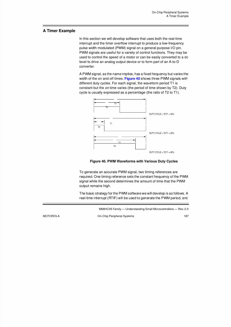
8/2/2019 122 Textbook
http://slidepdf.com/reader/full/122-textbook 187/331
On-Chip Peripheral Systems
A Timer Example
M68HC05 Family — Understanding Small Microcontrollers — Rev. 2.0
MOTOROLA On-Chip Peripheral Systems 187
A Timer Example
In this section we will develop software that uses both the real-time
interrupt and the timer overflow interrupt to produce a low-frequencypulse width modulated (PWM) signal on a general-purpose I/O pin.
PWM signals are useful for a variety of control functions. They may be
used to control the speed of a motor or can be easily converted to a dc
level to drive an analog output device or to form part of an A-to-D
converter.
A PWM signal, as the name implies, has a fixed frequency but varies the
width of the on and off times. Figure 40 shows three PWM signals with
different duty cycles. For each signal, the waveform period T1 is
constant but the on time varies (the period of time shown by T2). Dutycycle is usually expressed as a percentage (the ratio of T2 to T1).
Figure 40. PWM Waveforms with Various Duty Cycles
To generate an accurate PWM signal, two timing references are
required. One timing reference sets the constant frequency of the PWMsignal while the second determines the amount of time that the PWM
output remains high.
The basic strategy for the PWM software we will develop is as follows. A
real-time interrupt (RTIF) will be used to generate the PWM period, and
DUTY CYCLE = T2/T1 = 50%
DUTY CYCLE = T2/T1 = 20%
DUTY CYCLE = T2/T1 = 80%
T2
T1
T2
T1
T2
T1

8/2/2019 122 Textbook
http://slidepdf.com/reader/full/122-textbook 188/331
On-Chip Peripheral Systems
M68HC05 Family — Understanding Small Microcontrollers — Rev. 2.0
188 On-Chip Peripheral Systems MOTOROLA
the timer overflow (TOF) will be used to determine the PWM high time.
The rest of this chapter is a detailed development of this basic idea into
a working application.
Begin by taking a closer look at the MC68HC705J1A's timer. Figure 41shows the timer redrawn to emphasize the portion that we are interested
in. Conceptually, the eight counter stages surrounded by the gray box
form the timer that we will use to generate our PWM signal.
Examination of Figure 41 shows four counter stages between the timer
overflow interrupt output and the first input to the RTI rate select
multiplexer. This indicates that timer overflow interrupts will occur at a
rate 16 times faster than the fastest selectable real-time interrupt. Using
the RTI to generate the base frequency of a PWM signal and the TOF
interrupt to determine the duty cycle, we would be able to generate aPWM output with 16 discrete duty cycles (including 100%) as shown in
Figure 42. The numbers down the lefthand side of the figure indicate the
number of TOF interrupts that will occur before the PWM output is set
low. The numbers down the righthand side of the figure indicate the duty
cycle of the waveform. The alert reader will note that there is no TOF
interrupt count associated with the 100% duty cycle waveform. As will be
shown later, this is a special case that must be tested in the RTI routine.
Figure 41. Portion of the MC68HC705J1A Timer
MSB LSB
TIMER COUNT REGISTER
TOF RTIF TOFE RTIE RT1 RT0TOFR RTIFR
÷ 2
RTI RATE SELECT
TCSR
÷ 2 ÷ 2 ÷ 2 ÷ 2 ÷ 2 ÷ 2 ÷ 2 ÷ 2 ÷ 2 ÷ 2 ÷ 2 ÷ 2 ÷ 2

8/2/2019 122 Textbook
http://slidepdf.com/reader/full/122-textbook 189/331
On-Chip Peripheral Systems
A Timer Example
M68HC05 Family — Understanding Small Microcontrollers — Rev. 2.0
MOTOROLA On-Chip Peripheral Systems 189
Figure 42. PWM With 16 Discrete Duty Cycle Outputs
While the software to implement the illustrated PWM output is simple,
having only 16 choices for pulse width limits the usefulness of this PWMto a small number of applications (where accurate control is not
necessary). For example, if a motor speed control system was built
using this PWM, the target speed could only be controlled to 6.25%
(assuming that motor speed is directly proportional to the average
applied voltage). For most motor speed control applications, a 12.5%
variation in rotation speed would be unacceptable.
Obviously, much finer control of the PWM duty cycle is desired. One
approach might be to use a slower RTI rate. Using a slower RTI rate
would result in a greater number of TOF interrupts for each RTI. Forsome applications, this may be an acceptable solution. However, for
many applications the resulting frequency of the PWM waveform would
be too low to be of practical use. Table 18 shows the four available RTI
rates and the corresponding PWM frequency, the number of TOF
RTI INTERRUPTS
TOF INTERRUPTS
6.25%1
12.5%2
18.75%3
25.0%4
31.25%5
37.5%6
43.75%7
50.0%8
56.25%9
62.5%10
68.75%11
75.0%12
81.25%13
87.5%14
93.75%15
100% —

8/2/2019 122 Textbook
http://slidepdf.com/reader/full/122-textbook 190/331
On-Chip Peripheral Systems
M68HC05 Family — Understanding Small Microcontrollers — Rev. 2.0
190 On-Chip Peripheral Systems MOTOROLA
interrupts between RTIs, and the minimum variation in duty cycle that is
possible.
Table 18 seems to suggest that we are stuck trading off PWM frequency
for duty cycle accuracy. However, the following software program can
deliver much better results than expected.
Re-examining the portion of the timer in Figure 41 surrounded by the
gray box shows eight bits of the 15-bit timer chain. Four of the bits are
accessible to the CPU as the upper four bits of the TCR. The other four
bits form a divide-by-16 counter chain whose value is not directly
accessible. However, by counting the number of TOF interrupts that
occur after each RTI, we can always know the state of these four counter
bits. By using an 8-bit number to represent the PWM duty cycle, we can
achieve a duty cycle accuracy of 1 ÷ 255 or 0.4%.
To get this level of control with the MC68HC705J1A timer, we cannot
use an 8-bit duty cycle value directly. The 8-bit number must be
separated into two components. One component will represent the value
of the inaccessible four bits of the counter (the number of TOF interrupts
that occur after each RTI). The other component will represent the value
of the upper four bits of the TCR (the lower four bits of our counter that
are directly accessible to the CPU).
To make these two components easy for the software to use, the upperfour bits of the desired PWM duty cycle must be placed in the lower four
bits of a variable we will call PWMCoarse. This value will be used to
determine during which TOF interrupt the PWM output should be set
low. The lower four bits of the desired PWM duty cycle will be placed in
the upper four bits of a variable we will call PWMFine. This value is used
Table 18. PWM Characteristics for Various RTI Rates
RTI RatePWM
FrequencyTOF
InterruptsMinimum Duty
Cycle
8.2 ms 122 Hz 16 6.25%
16.4 ms 61.0 Hz 32 3.125%
32.8 ms 30.5 Hz 64 1.56%
65.5 ms 15.3 Hz 128 0.78%

8/2/2019 122 Textbook
http://slidepdf.com/reader/full/122-textbook 191/331
On-Chip Peripheral Systems
A Timer Example
M68HC05 Family — Understanding Small Microcontrollers — Rev. 2.0
MOTOROLA On-Chip Peripheral Systems 191
within the TOF interrupt to determine precisely when during the TOF
interrupt the PWM output should be set low. By comparing the value in
PWMFine to the upper four bits of the TCR, we can effectively divide
each TOF interrupt into 16 separate time intervals as shown in
Figure 43.
Figure 43. Each TOF Interrupt Sliced into 16 Separate
Time Intervals
Now that we have described the theory involved in generating an
accurate PWM waveform using the MC68HC05J1A's timer, the next
step is to write the software. We begin by generating flowcharts to
describe the actions necessary to produce the PWM waveform and
finish by translating the flowcharts into M68HC05 assembly language.
The flowcharts in Figure 44, Figure 45, and Figure 46 describe thePWM software. The flowchart in Figure 45, although simple, is included
for completeness and clarity. Because the MC68HC05J1A contains only
one timer interrupt vector, a short routine must determine whether a
timer interrupt was caused by a TOF or an RTIF interrupt and then
branch to the appropriate service routine.
RTI INTERRUPTS
TOF INTERRUPTS
RTI
TOF INTERRUPTS

8/2/2019 122 Textbook
http://slidepdf.com/reader/full/122-textbook 192/331
On-Chip Peripheral Systems
M68HC05 Family — Understanding Small Microcontrollers — Rev. 2.0
192 On-Chip Peripheral Systems MOTOROLA
Figure 44. Timer Interrupt Service Routine
As shown in Figure 45, the RTIF interrupt routine checks for two special
conditions, 0% and 100% duty cycle. It then sets up the PWMFine and
PWMCoarse variables for use by the TOF interrupt service routine. If a
0% duty cycle is desired, the PWM output is set low and the RTIF
interrupt service routine immediately returns. If a 100% duty cycle is
desired, the PWM output is set high and the RTIF interrupt service
routine will return immediately. If a duty cycle between 0% and 100% is
desired, the variable DesiredPWM is split into the two components,
PWMFine and PWMCoarse. If the resulting value of PWMCoarse is 0the program will jump to the second part of the TOF interrupt routine,
which continually compares the value in PWMFine to the upper four bits
of the TCR. If the value of PWMCoarse is not 0, TOF interrupts are
enabled and the RTIF interrupt routine returns.
BEGIN TIMER
INTERRUPT SERVICE
TOF INTERRUPT ?
NO
YES
RTIF INTERRUPT ?
NO
YES
RETURN
GO EXECUTE TOFINTERRUPT ROUTINE
(FIGURE 46)
GO EXECUTE RTIFINTERRUPT ROUTINE
(FIGURE 45)

8/2/2019 122 Textbook
http://slidepdf.com/reader/full/122-textbook 193/331
On-Chip Peripheral Systems
A Timer Example
M68HC05 Family — Understanding Small Microcontrollers — Rev. 2.0
MOTOROLA On-Chip Peripheral Systems 193
Figure 45. Real-Time Interrupt Routine Flowchart
BEGIN RTIF
INTERRUPT ROUTINE
DesiredPWM = 0% ?
NO
YES
RETURN FROM
INTERRUPT
PWM OUTPUT = 0
RESET RTIF
INTERRUPT FLAG
PWM OUTPUT = 1
DesiredPWM = 100% ?
NO
YES
PWMFine = DesiredPWM <<4
PWMCourse = DesiredPWM >>4
PWMCourse = 0 ?
NO
YES
CLEAR TOF INTERRUPT FLAG
ENABLE TOF INTERRUPTS
EXECUTE SECOND
PART OF TOF INTERRUPT
A
SEE FIGURE 46

8/2/2019 122 Textbook
http://slidepdf.com/reader/full/122-textbook 194/331
On-Chip Peripheral Systems
M68HC05 Family — Understanding Small Microcontrollers — Rev. 2.0
194 On-Chip Peripheral Systems MOTOROLA
The flowchart in Figure 46 describes the actions required for the TOF
interrupt routine. The first action is to decrement the value of
PWMCoarse. When PWMCoarse becomes 0, it means that the value in
the upper four bits of our counter is equal to the upper four bits of
DesiredPWM. Next, we continually compare the upper four bits of the
TCR with the value of PWMFine (which is the lower four bits of
DesiredPWM). When these two values match, the PWM output is set
low, the TOF interrupt is reset and disabled, and the TOF interrupt
returns.
Figure 46. Timer Overflow Interrupt Flowchart
Listing 5. PWM Program Listing shows the assembly language listing
for the three routines described by the flowcharts in Figure 44,
Figure 45, and Figure 46. The translation of the flowcharts into
assembly language is fairly straightforward. The possible exception is
the assembly code in the RTIF interrupt routine that splits the
BEGIN TOF
INTERRUPT ROUTINE
PWMCourse = 0 ?
YES
NO
RETURN FROM
INTERRUPT
RESET TOFINTERRUPT FLAG
TCR ≥ PWMFine ?
YES
NO
SET PWM OUTPUT = 0
RESET & DISABLETOF INTERRUPT
A
PWMCourse = PWMCourse – 1
FROMFIGURE 45

8/2/2019 122 Textbook
http://slidepdf.com/reader/full/122-textbook 195/331
On-Chip Peripheral Systems
A Timer Example
M68HC05 Family — Understanding Small Microcontrollers — Rev. 2.0
MOTOROLA On-Chip Peripheral Systems 195
DesiredPWM variable into the PWMCoarse and PWMFine components.
This routine works by using a combination of shift left and rotate left
instructions that operate on the A and the X registers. The LSLA
instruction shifts the most significant bit of the A register into the carry
and a 0 into the least significant bit of A. The ROLX instruction places
the carry (from the previous LSLA instruction) into the least significantbit
of the X register. After the execution of four of these instruction pairs, the
four most significant bits of the A register (DesiredPWM) will end up in
the least significant four bits of the X register (PWMCoarse). The least
significant four bits of the A register will end up in the most significant
four bits of the A register (PWMFine).
Using the PWM
Software
In normal circumstances, the PWM software of Listing 5. PWM
Program Listing would be used as a part of a larger program.The value
of DesiredPWM would be generated by some other part of the main
program. To demonstrate the PWM software, the value of DesiredPWM
was arbitrarily set to $80 (12810) by program instructions. If a simulator
or emulator is used to study this program, you can change the value of
DesiredPWM and observe the effect.
The PWM program is interrupt driven. This means that the timer
generates interrupt requests for the CPU to stop processing the main
program and respond to the interrupt request. Since the demonstrationversion of this program in Listing 5. PWM Program Listing has no
other main program to perform, a “branch to here” instruction was
included after the clear interrupt mask (CLI) instruction. This instruction
is an infinite loop. Timer interrupts will cause the CPU to periodically
leave this infinite loop to respond to the timer requests and then return
to executing the infinite loop.

8/2/2019 122 Textbook
http://slidepdf.com/reader/full/122-textbook 196/331
On-Chip Peripheral Systems
M68HC05 Family — Understanding Small Microcontrollers — Rev. 2.0
196 On-Chip Peripheral Systems MOTOROLA
Listing 5. PWM Program Listing (Sheet 1 of 2)
Listing5. PWMProgram Listing
;Equates for all 705J1 are included but not shown
; in this listing
;
0000 Percent100 EQU $FF ;DesiredPWM value for 100% duty0000 PWM EQU PA7 ;PWM output on port A bit 7
; ;update the DesiredPWM variable.
00C0 ORG RAMStart
00C0 DesiredPWM RMB 1 ;Desired PWM duty cycle...
; expressed as the numerator of DesiredPWM/255.
; 0 = continuous low 255 = continuous high.
00C1 PWMCoarse RMB 1 ;Number of TOF interrupts...
; before we start to compare PWMFine to value in the TCR.
00C2 PWMFine RMB 1 ;When TCR matches PWMFine,...
; ; the PWM is set low.; PWMFine is derived from the lower 4 bits of DesiredPWM.
; These 4 bits are placed in the upper 4 bits of PWMFine.
00C3 VarEnd EQU *
;********************************************************
;
0300 ORG ROMStart
;
0300 Start EQU *
0300 9C RSP ;Reset the stack pointer
0301 3F00 CLR PORTA ;Set Port A outputs to all 0's
0303 A6FF LDA #$FF ;Make all Port A's pins outputs
0305 B704 STA DDRA
;Clear out all of RAM
0307 AEC0 LDX #RAMStart ;Point to the start of RAM
0309 7F ClrLoop CLR ,X ;Clear a byte
030A 5C INCX ;Point to the next location
;Cleared the last location?
030B 26FC BNE ClrLoop ;No, Continue to clear RAM
030D A680 LDA #$80 ;Corresponds to 50% (128/255)
030F B7C0 STA DesiredPWM ;Establish a PWM duty cycle
0311 A61C LDA #$1C ;Clear timer ints...
0313 B708 STA TSCR ;and enable RTIF interrupt
0315 9A CLI ;Enable interrupts
0316 20FE BRA * ;Infinite loop, PWM uses ints
;********************************************************
;RTI sets period. @2MHz & RT1:RT0 = 0:0, period = 8.192 ms
;or about 122 Hz
0318 TimerInt EQU *
0318 0E0804 BRSET TOF,TSCR,TOFInt ;TOF interrupt?
031B 0C0812 BRSET RTIF,TSCR,RTIInt ;RTI interrupt?
031E 80 RTI
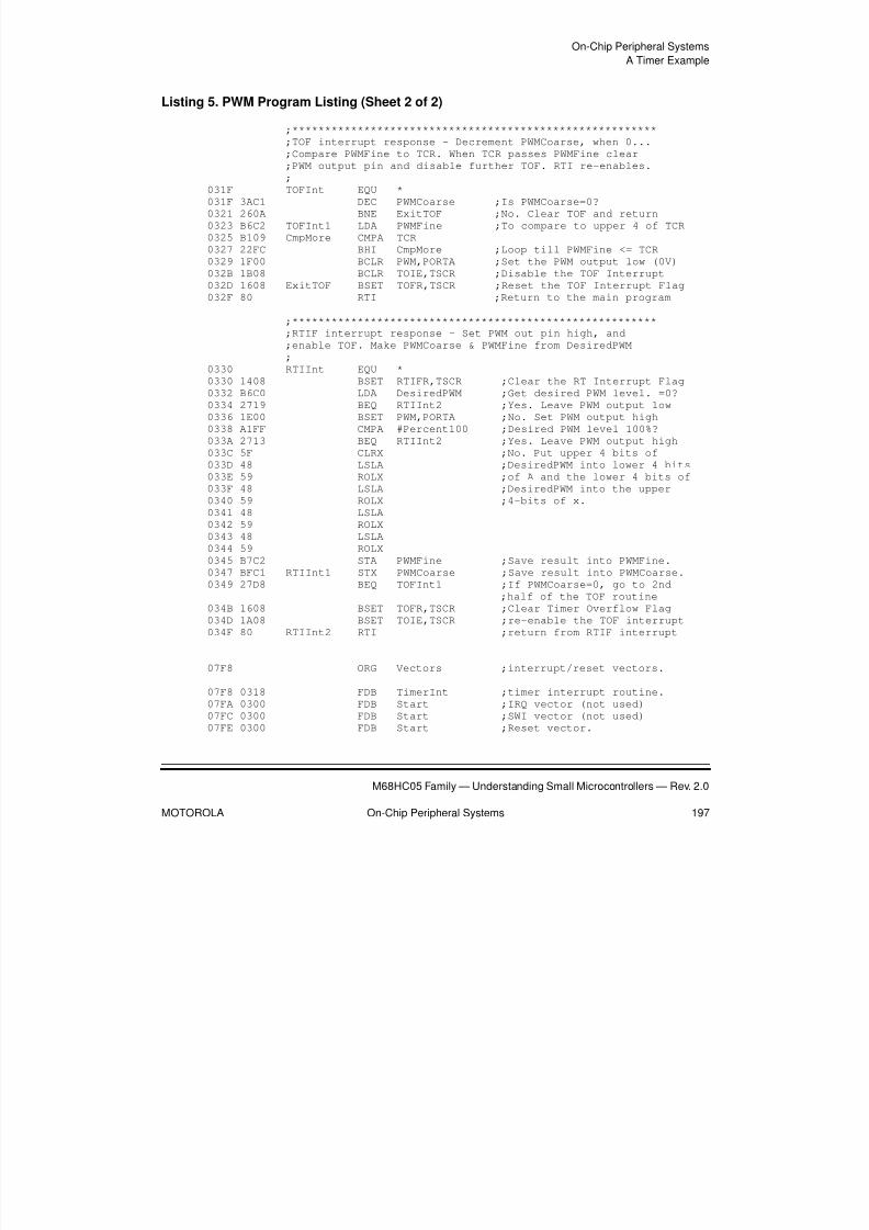
8/2/2019 122 Textbook
http://slidepdf.com/reader/full/122-textbook 197/331
On-Chip Peripheral Systems
A Timer Example
M68HC05 Family — Understanding Small Microcontrollers — Rev. 2.0
MOTOROLA On-Chip Peripheral Systems 197
Listing 5. PWM Program Listing (Sheet 2 of 2)
;********************************************************
;TOF interrupt response - Decrement PWMCoarse, when 0...
;Compare PWMFine to TCR. When TCR passes PWMFine clear
;PWM output pin and disable further TOF. RTI re-enables.;
031F TOFInt EQU *
031F 3AC1 DEC PWMCoarse ;Is PWMCoarse=0?
0321 260A BNE ExitTOF ;No. Clear TOF and return
0323 B6C2 TOFInt1 LDA PWMFine ;To compare to upper 4 of TCR
0325 B109 CmpMore CMPA TCR
0327 22FC BHI CmpMore ;Loop till PWMFine <= TCR
0329 1F00 BCLR PWM,PORTA ;Set the PWM output low (0V)
032B 1B08 BCLR TOIE,TSCR ;Disable the TOF Interrupt
032D 1608 ExitTOF BSET TOFR,TSCR ;Reset the TOF Interrupt Flag
032F 80 RTI ;Return to the main program
;********************************************************
;RTIF interrupt response - Set PWM out pin high, and;enable TOF. Make PWMCoarse & PWMFine from DesiredPWM
;
0330 RTIInt EQU *
0330 1408 BSET RTIFR,TSCR ;Clear the RT Interrupt Flag
0332 B6C0 LDA DesiredPWM ;Get desired PWM level. =0?
0334 2719 BEQ RTIInt2 ;Yes. Leave PWM output low
0336 1E00 BSET PWM,PORTA ;No. Set PWM output high
0338 A1FF CMPA #Percent100 ;Desired PWM level 100%?
033A 2713 BEQ RTIInt2 ;Yes. Leave PWM output high
033C 5F CLRX ;No. Put upper 4 bits of
033D 48 LSLA ;DesiredPWM into lower 4 bits
033E 59 ROLX ;of A and the lower 4 bits of
033F 48 LSLA ;DesiredPWM into the upper
0340 59 ROLX ;4-bits of x.0341 48 LSLA
0342 59 ROLX
0343 48 LSLA
0344 59 ROLX
0345 B7C2 STA PWMFine ;Save result into PWMFine.
0347 BFC1 RTIInt1 STX PWMCoarse ;Save result into PWMCoarse.
0349 27D8 BEQ TOFInt1 ;If PWMCoarse=0, go to 2nd
;half of the TOF routine
034B 1608 BSET TOFR,TSCR ;Clear Timer Overflow Flag
034D 1A08 BSET TOIE,TSCR ;re-enable the TOF interrupt
034F 80 RTIInt2 RTI ;return from RTIF interrupt
07F8 ORG Vectors ;interrupt/reset vectors.
07F8 0318 FDB TimerInt ;timer interrupt routine.
07FA 0300 FDB Start ;IRQ vector (not used)
07FC 0300 FDB Start ;SWI vector (not used)
07FE 0300 FDB Start ;Reset vector.

8/2/2019 122 Textbook
http://slidepdf.com/reader/full/122-textbook 198/331
On-Chip Peripheral Systems
M68HC05 Family — Understanding Small Microcontrollers — Rev. 2.0
198 On-Chip Peripheral Systems MOTOROLA
A Practical Motor Control Example
In this section,we will develop a practical application by expanding some
of the software developed in this book. The example will add someexternal hardware to the MC68HC705K1 so that we can observe the
effects of our software on the world outside the microcontroller. We will
use a slightly modified version of the PWM routine that was developed
in this chapter to control the speed of a small permanent-magnet direct
current (DC) motor. In addition, we will use the concepts developed in
the chapter titled On-Chip Peripheral Systems that allow the CPU to
read the state of switches connected to the MCU’s general-purpose I/O
pins.
Theory DC motors are often the best choice for variable-speed motor
applications. Brush DC motors are the easiest to control electronically.
Electronic control of brushless DC, stepper, AC induction, and switched
reluctance motors all require more-complex control circuits in addition to
more power-switching devices. Small, low-cost brush DC motors are
available off the shelf for many low-volume applications where custom
designs would be too expensive. The reliability of brush motors is
adequate for most applications. However, eventually, the brushes will
wear out and need to be replaced.
To vary the speed of a brush DC motor, we must vary the voltage that is
applied to the motor. Several approaches can be used to accomplish
this. We will examine several of the methods, explaining the major
advantages and disadvantages of each.
The first and most obvious approach to varying the voltage applied to a
motor might be to place a variable resistor in series with the motor and
the power source, as shown in Figure 47. While this approach is very
simple, it has some serious disadvantages. First, the resistor’s power
dissipation capabilities must be matched to the power requirements ofthe motor. For very small fractional-horsepower DC motors, the size of
the variable resistor will be quite modest. However, as the size of the
motor increases, the motor’s power requirement increases and the size
and cost of the variable resistor will increase.

8/2/2019 122 Textbook
http://slidepdf.com/reader/full/122-textbook 199/331
On-Chip Peripheral Systems
A Practical Motor Control Example
M68HC05 Family — Understanding Small Microcontrollers — Rev. 2.0
MOTOROLA On-Chip Peripheral Systems 199
Figure 47. Motor Speed Controlled by a Variable Resistor
The second major disadvantage of this type of speed control is the
inability to automatically adjust the speed of the motor to compensate for
varying loads. This is a primary disadvantage for applications that
require precise speed control under varying mechanical loads.
An electronic variation of the variable resistor form of speed control is
shown in Figure 48. In this arrangement, we have replaced the variableresistor with a transistor. Here, the transistor is operated in its linear
mode. When a transistor operates in this mode, it essentially behaves as
an electrically controlled variable resistor. By applying a proportional
analog control signal to the transistor, the "resistivity" of the transistor
can be varied, which will in turn vary the speed of the motor. By using a
transistor to control the speed of the motor in this manner, the magnitude
of the control signal is reduced to much lower voltage and current levels
that can be readily generated by electronic circuity.
Figure 48. Motor Speed Controlled by a Transistor
Unfortunately, using a transistor in its linear mode still retains a major
disadvantage of using a variable resistor. Like a variable resistor, a
MOTOR
M
MOTOR
M
RB
VBB

8/2/2019 122 Textbook
http://slidepdf.com/reader/full/122-textbook 200/331
On-Chip Peripheral Systems
M68HC05 Family — Understanding Small Microcontrollers — Rev. 2.0
200 On-Chip Peripheral Systems MOTOROLA
power transistor operating in its linear region will have to dissipate large
amounts of power under varying speed and load conditions. Even
though power transistors capable of handling high power levels are
widely available at relatively modest prices, the power dissipated by the
transistor will usually require a large heat sink to prevent the device from
destroying itself.
In addition to being operated as a linear device, transistors also may be
operated as electronic switches. By applying the proper control signal to
a transistor, the device will either be turned on or turned off. As shown in
Figure 49, when the transistor is turned on, it will essentially behave as
a mechanical switch allowing electric current to pass through it and its
load virtually unimpeded. When turned off, no current passes through
the transistor or its load. Because the transistor dissipates very little
power when it is fully turned on or saturated, the device operates in an
efficient manner.
Figure 49. Transistor Used as an Electronic Switch
It would seem that, when using a transistor to control the speed of a DC
motor, we are stuck using the device in its inefficient linear mode if we
want a motor to operate at something other than full speed. Fortunately,there is an alternative method of controlling the speed of a DC motor
using a transistor. By using the transistor as an electronically controlled
switch and applying a PWM control signal of sufficient frequency,we can
control the speed of the motor. To help understand how turning a motor
M
TRANSISTOR “ON”
M
TRANSISTOR “OFF”
VCCVCCIC
RB
VBBVCE ≅ 0 VOLTS
IC = 0
VCE = VCCRB
VBB = 0
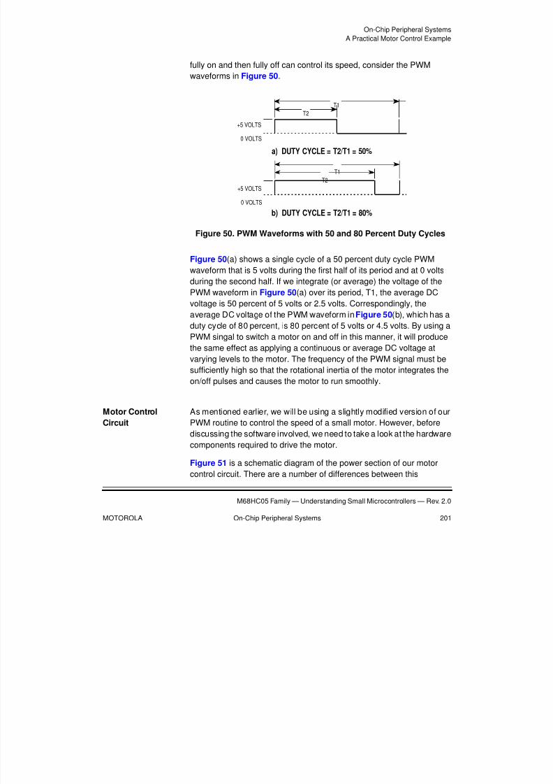
8/2/2019 122 Textbook
http://slidepdf.com/reader/full/122-textbook 201/331
On-Chip Peripheral Systems
A Practical Motor Control Example
M68HC05 Family — Understanding Small Microcontrollers — Rev. 2.0
MOTOROLA On-Chip Peripheral Systems 201
fully on and then fully off can control its speed, consider the PWM
waveforms in Figure 50.
Figure 50. PWM Waveforms with 50 and 80 Percent Duty Cycles
Figure 50(a) shows a single cycle of a 50 percent duty cycle PWM
waveform that is 5 volts during the first half of its period and at 0 volts
during the second half. If we integrate (or average) the voltage of the
PWM waveform in Figure 50(a) over its period, T1, the average DC
voltage is 50 percent of 5 volts or 2.5 volts. Correspondingly, the
average DC voltage of the PWM waveform in Figure 50(b), which has aduty cycle of 80 percent, is 80 percent of 5 volts or 4.5 volts. By using a
PWM singal to switch a motor on and off in this manner, it will produce
the same effect as applying a continuous or average DC voltage at
varying levels to the motor. The frequency of the PWM signal must be
sufficiently high so that the rotational inertia of the motor integrates the
on/off pulses and causes the motor to run smoothly.
Motor Control
Circuit
As mentioned earlier, we will be using a slightly modified version of our
PWM routine to control the speed of a small motor. However, beforediscussing the software involved, we need to take a look at the hardware
components required to drive the motor.
Figure 51 is a schematic diagram of the power section of our motor
control circuit. There are a number of differences between this
a) DUTY CYCLE = T2/T1 = 50%
b) DUTY CYCLE = T2/T1 = 80%
T2
T1
T2T1
0 VOLTS
+5 VOLTS
0 VOLTS
+5 VOLTS

8/2/2019 122 Textbook
http://slidepdf.com/reader/full/122-textbook 202/331
On-Chip Peripheral Systems
M68HC05 Family — Understanding Small Microcontrollers — Rev. 2.0
202 On-Chip Peripheral Systems MOTOROLA
schematic and the conceptual ones used in Figure 48 and Figure 49.
We will describe these differences in the following paragraphs.
The most noticeable difference is the schematic symbol for the power
transistor that will be used as an electronic switch. This device is a powerMOSFET. Unlike the bipolar transistor shown in Figure 48 and
Figure 49, this special type of transistor is controlled by the magnitude
of a voltage applied to its gate. Additionally, this particular power
MOSFET, the MTP3055EL, may be completely saturated with only 5
volts applied to its gate. These two characteristics allow this device to be
controlled directly by a microcontroller’s output pin for many
applications.
Because the input iimpedance of a power MOSFET is very high (greater
than 40 megaohms), a 10 KΩ resistor is placed between the MOSFETgate and ground to prevent erratic operation of the motor should the
connection between the microcontroller and the gate ever become cut.
The 15-volt zener diode is placed in parallel with the resistor to protect
the gate of the MOSFET from possible damage from high voltage
transients that may be generated in the system. The 1N4001 diode in
parallel with the motor is used to snub the inductive kick of the motor
each time the MOSFET is turned off. The 0.1-µf capacitor in parallel with
the motor is used to reduce the electrical noise generated by the motor’s
brushes.
For further information on designing with power MOSFETs, it is
suggested that the reader study the Theory and Applications section of
the Motorola Power MOSFET Transistor Data Book (DL153).
Figure 52 is a schematic diagram of the microprocessor section of the
circuit that we will be using in this example. In addition to generating a
PWM output, the MC68HC705K1 is reading three momentary
pushbutton switches connected to its I/O pins. As the schematic shows,
a single switch turns the motor on and off while two switches set the
speed of the motor.

8/2/2019 122 Textbook
http://slidepdf.com/reader/full/122-textbook 203/331
On-Chip Peripheral Systems
A Practical Motor Control Example
M68HC05 Family — Understanding Small Microcontrollers — Rev. 2.0
MOTOROLA On-Chip Peripheral Systems 203
Figure 51. Power Section of the Motor Speed Control Circuit
Figure 52. Microcontroller Section
of the Motor Speed Control Circuit
M
MTP3055EL15 V10 k
1N40010.1 F
+5 V
FROM PA7 OFMC68HC705K1
10 M
0.1 F
+5 V
TO GATE OF
MTP3055EL
27 pF
27 pF
4 MHz
VDDVSS
PA7PA0
PA1
PA2
ON/OFF
SPEEDDOWN
SPEEDUP
10 k
(5)
IRQ
MC68HC705K1+5 V
MOTORCONTROL
SWITCHES
OSC1
OSC2RESET

8/2/2019 122 Textbook
http://slidepdf.com/reader/full/122-textbook 204/331
On-Chip Peripheral Systems
M68HC05 Family — Understanding Small Microcontrollers — Rev. 2.0
204 On-Chip Peripheral Systems MOTOROLA
One side of each switch is connected to circuit ground, while the other
side of the switch is connected to an I/O pin on the MC68HC705K1
microcontroller. Each of the input pins on the microcontroller is "pulled
up" through a 10-kΩ resistor to +5 volts. These 10-kΩ pullup resistors
keep each of the three input pins at a logic 1 when the pushbutton
switches are not pressed.
In this exampel circuit, the switch controls will operate in the following
manner. The motor on/off switch operates as an alternate-action control.
Each time the switch is pushed and released, the motor will alternately
be turned on or off. When the motor is turned on, its speed will be set to
the speed it was going the last time the motor was on.
The speed up and speed down switches increase or decrease motor
speed, respectively. To increase or decrease the speed of the motor, therespective switch must be pressed and held. The motor speed PWM will
be increased or decreased at a rate of approximately 0.4 percent every
24 ms. This "ramp" rate will allow the motor speed to be adjusted across
its entire speed range in approximately six seconds.
Motor Control
Software
Figure 53 shows a flowchart that describes the new RTI interrupt
software. The only functional change to the PWM routine developed
earlier in this chapter is the addition of one instruction at the beginning
of the RTI interrupt service routine. This instruction decrements thevariable RTIDlyCnt. This variable is used by the three routines that read
the input switches to develop a switch debounce delay.
As mentioned in the Programming chapter, there are usually many
ways to perform a specific task using the microcontroller’s instruction
set. To demonstrate this, onepart of the revised RTI interrupt routine has
been impmlemented in a slightly different manner. Remember, looking
at Listing 6. Speed Control Program Listing, that we had to split the
variable DesiredPWM into two parts, PWMFine and PWMCoarse. To do
this, we used a combination of shifts and rotates to place the upper four
bits of the A accumulator (DesiredPWM) into the lower four bits of the X
register (PWMCoarse) and the lower four bits of A into the upper four bits
of A (PWMFine). This method required nine bytes of program memory
and 26 CPU cycles.

8/2/2019 122 Textbook
http://slidepdf.com/reader/full/122-textbook 205/331
On-Chip Peripheral Systems
A Practical Motor Control Example
M68HC05 Family — Understanding Small Microcontrollers — Rev. 2.0
MOTOROLA On-Chip Peripheral Systems 205
Figure 53. Revised RTI Routine Flowchar
BEGIN RTIFINTERRUPT ROUTINE
DesiredPWM = 0% ?
NO
YES
RETURN FROMINTERRUPT
PWM OUTPUT = 0
RESET RTIFINTERRUPT FLAG
PWM OUTPUT = 1
DesiredPWM = 100% ?
NO
YES
PWMFine = DesiredPWM <<4
PWMCourse = DesiredPWM >>4
PWMCourse = 0 ?NO
YES
CLEAR TOF INTERRUPT FLAG
ENABLE TOF INTERRUPTS
GO EXECUTE SECOND
PART OF TOF INTERRUPT
A
see Figure 9-8
RTIDlyCnt = RTIDlyCnt – 1

8/2/2019 122 Textbook
http://slidepdf.com/reader/full/122-textbook 206/331
On-Chip Peripheral Systems
M68HC05 Family — Understanding Small Microcontrollers — Rev. 2.0
206 On-Chip Peripheral Systems MOTOROLA
By using the alternative approach in Listing 6. Speed Control
Program Listing, we can get the same result in only three bytes of
program memory and 13 CPU cycles.
The RTIInt routine in Listing 6. Speed Control Program Listingdemonstrates the alternative approach. The original 9-byte instrtuction
sequence has been replaced with two instructions, LDX #16 and MUL.
The MUL instruction multiples the value in the accumulator by the value
in the index register and places the result in X:A (concatenation of X and
A). Multiplying a binary number by 16 is equivalent to shifting the value
left by four positions. Just as in the original implementation, the upper
four bits of DesiredPWM are now in the lower four bits of the X register
(PWMCoarse) and the lower four bits of the A register have been moved
into the upper four bits a A (PWMFine).
The flowchart in Figure 54 describes the main loop routine of our motor
control module. This module checks the state of each of the three input
switches. If any one of the three switches is pressed, a routine that
handles the actions for that switch is called. If there are no switches
pressed, the main loop is repeated.
Figure 54. Flowchart for Main Program Loop
BEGINMAIN PROGRAM
MOTOR ON/OFF SW. PRESSED ?
NO
YESTURN MOTOR ON / OFF
SPEED UP SW. PRESSED ?
NO
YESINCREASE MOTOR SPEED
SPEED DOWN SW. PRESSED ?NO
YES
DECREASE MOTOR SPEED

8/2/2019 122 Textbook
http://slidepdf.com/reader/full/122-textbook 207/331
On-Chip Peripheral Systems
A Practical Motor Control Example
M68HC05 Family — Understanding Small Microcontrollers — Rev. 2.0
MOTOROLA On-Chip Peripheral Systems 207
Figure 55, Figure 56, and Figure 57 are flowcharts for the three
routines that handle the actions of the three input switches. Each of
these routines begins with the execution of a 50-ms switch debounce
routine. As decribed in the Programming chapter, this delay is required
because the mechanical bounce produced by the closure of a switch is
seen by the microcontroller as multiple switch closures during the first
several milliseconds after the switch is pressed. This small section of
code stores the value DebounceDly into the variable RTIDlyCnt and then
waits until the value is decremented to zero by the RTI interrupt service
routine. When the value reaches zero, the switch is again checked to be
sure a valid switch closure occurred. The value used for the delay
constant (DebounceT) will produce a minimum delay of approximately
50 milliseconds.
The flowchart in Figure 55 describes the MotorOnOff routine. It is
responsible for handling the actions of the alternate action switch that
turns the motor on and off. After the switch debounce delay, this routine
waits until the on/off switch is released before it performs the rest of its
task and returns to the main loop. Otherwise, the main loop would detect
another switch closure as soon as the MotorOnOff program finished and
returned to the main program loop.
The routines described by the flowcharts in Figure 56 and Figure 57
operate in essentially the same manner. First, each of these routines
checks to see if the motor is currently turned on. If the motor is off, the
routine returns to the main program loop. Each routine then loops
continuously as long as its associated switch remains pressed. Each
time through the loop, the MotorPWM and DesiredPWM variables are
incremented or decremented to increase or decrease the duty cycle of
the PWM output. To keep the speed of the motor from increasing or
decreasing too rapidly when a switch is pressed, a delay of
approprixmately 25 ms is inserted each time through the loop. This
25-ms delay allows the motor to be adjusted across its entire speed
range in approximately six seconds.
Listing 6. Speed Control Program Listing contains the assembly
language listing for the routines described by the flowcharts in Figure 46
and Figure 53 through Figure 57.

8/2/2019 122 Textbook
http://slidepdf.com/reader/full/122-textbook 208/331
On-Chip Peripheral Systems
M68HC05 Family — Understanding Small Microcontrollers — Rev. 2.0
208 On-Chip Peripheral Systems MOTOROLA
Figure 55. Flowchart for MotorOn/Off Routine
TURN MOTOR
ON OR OFF
MOTOR ON/OFF SW. PRESSED ?
YES
NO
RETURN
TURN MOTOR ON
BY SETTING
DesiredPWM = LAST SPEED
MOTOR ON ?
YES
NO
TURN MOTOR OFF
BY SETTING
DesiredPWM = 0
MOTOR ON/OFF SW. PRESSED ?
NO
YES
DEBOUNCE FOR 50 ms

8/2/2019 122 Textbook
http://slidepdf.com/reader/full/122-textbook 209/331
On-Chip Peripheral Systems
A Practical Motor Control Example
M68HC05 Family — Understanding Small Microcontrollers — Rev. 2.0
MOTOROLA On-Chip Peripheral Systems 209
Figure 56. Flowchart for Motor Speed-Up Routine
Figure 57. Flowchart for Motor Speed-Down Routine
INCREASEMOTOR SPEED
SPEED UP SW. PRESSED ?
YES
NO
RETURN
MotorPWM = MotorPWM + 1DesiredPWM = DesiredPWM +1
MOTOR PWM AT 100% ?
YES
NO
DEBOUNCE FOR 50 ms
MOTOR ON ?YES
NO
DELAY FOR ABOUT 25 ms
DECREASEMOTOR SPEED
SPEED DOWN SW. PRESSED ?
YES
NO
RETURN
MotorPWM = MotorPWM – 1DesiredPWM = DesiredPWM –1
MOTOR PWM AT MinPWM ?
YES
NO
DEBOUNCE FOR 50 ms
MOTOR ON ?YES
NO
DELAY FOR ABOUT 25 ms

8/2/2019 122 Textbook
http://slidepdf.com/reader/full/122-textbook 210/331
On-Chip Peripheral Systems
M68HC05 Family — Understanding Small Microcontrollers — Rev. 2.0
210 On-Chip Peripheral Systems MOTOROLA
Listing 6. Speed Control Program Listing (Sheet 1 of 5)
Listing 6. Speed Control Program Listing
;Equates for all 705K1 are included but not shown
00FF Percent100 EQU $FF ;DesiredPWM value for 100% duty
0003 RampTime EQU 3 ;Speed up/down ramp constant
0007 DebounceT EQU 7 ;Switch debounce constant
0010 MinPWM EQU $10 ;Minimum PWM value.
0007 PWM EQU PA7 ;Port A bit 7 is PWM output
0000 MotorOnOff EQU PA0 ;Sw. for the Motor On/Off
0001 SpeedUp EQU PA1 ;Sw. for raising the speed
0002 SpeedDn EQU PA2 ;Sw. for lowering the speed
00E0 ORG RAMStart
00E0 DesiredPWM RMB 1 ;Desired PWM/255 = duty cycle
;0 = continuous low;255 = continuous high
00E1 PWMCoarse RMB 1 ;Number of TOFs before...
;start watching PWMFine vs TCR
00E2 PWMFine RMB 1 ;When TCR matches PWMFine,...
;set PWM output low
00E3 MotorPWM RMB 1 ;Last PWM/speed while motor.on
00E4 RTIDlyCnt RMB 1 ;Decremented on each RTI...
;used to debounce switches
00E5 MotorOnFlg RMB 1 ;1 = PWM out is on / 0 = off
00E6 VarEnd EQU *
;*********************************************************
0200 ORG ROMStart
0200 Start EQU *
0200 9C RSP ;Reset stack pointer in case...
;we got here from an error
0201 3F 00 CLR PortA ;Set up Port A outs to all 0's
0203 A6 80 LDA #$80 ;Make PA7 an output
0205 B7 04 STA DDRA
;Clear out all of RAM
0207 AE E0 LDX #RAMStart;Point to the start of RAM
0209 7F ClrLoop CLR 0,x ;Clear a byte.
020A 5C INCX ;Point to the next loc./ done?

8/2/2019 122 Textbook
http://slidepdf.com/reader/full/122-textbook 211/331
On-Chip Peripheral Systems
A Practical Motor Control Example
M68HC05 Family — Understanding Small Microcontrollers — Rev. 2.0
MOTOROLA On-Chip Peripheral Systems 211
Listing 6. PWM Program Listing (Sheet 2 of 5)
020B 26 FC BNE ClrLoop ;No; continue to clear RAM
020D A6 1C LDA #$1C ;Enable TOF & RTI interrupts
020F B7 08 STA TSCR
0211 A6 10 LDA #MinPWM ;Initialize PWM to min speed
0213 B7 E3 STA MotorPWM
0215 9A CLI ;Enable interrupts
;*********************************************************
;Main program loop. Read motor control switches. If a
; switch is pressed, BSR to perform the requested action.
; Loop continuously looking for switch closures.
;
0216 00 00 02 Main BRSET MotorOnOff,PortA,Main1 ;On/Off pressed?
0219 AD 0C BSR DoOnOff ;If yes, go to DoOnOff
021B 02 00 02 Main1 BRSET SpeedUp,PortA,Main2 ;Speed Up pressed?
021E AD 25 BSR DoSpeedUp ;If yes, go to DoSpeedUp
0220 04 00 F3 Main2 BRSET SpeedDn,PortA,Main ;Speed Down ?
0223 AD 44 BSR DoSpeedDn ;If yes, go to DoSpeedDown
0225 20 EF BRA Main ;Repeat loop continuously
;*********************************************************
;DoOnOff handles the closure of the Motor On/Off switch
; Debounces switch and waits for release.
;
0227 DoOnOff EQU *
0227 A6 07 LDA #DebounceT ;DebounceT * RTI time = 50mS
0229 B7 E4 STA RTIDlyCnt ;Initialize software counter
022B 3D E4 DoOnOff1 TST RTIDlyCnt ;RTI interrupt decrements it
022D 26 FC BNE DoOnOff1 ;Loop till RTIDlyCnt = 0022F 00 00 12 BRSET MotorOnOff,PortA,DoOnOff3 ;Then check sw
;If open, not a good press
0232 01 00 FD BRCLR MotorOnOff,PortA,* ;Wait for sw release
0235 3D E5 TST MotorOnFlg ;Motor already on?
0237 26 07 BNE DoOnOff2 ;Yes, turn the motor off.
0239 3C E5 INC MotorOnFlg ;No, Set ‘MotorOn’ flag
023B B6 E3 LDA MotorPWM ;And get last motor speed
023D B7 E0 STA DesiredPWM ;Turns on the PWM output
023F 81 RTS ;Return (1 of 2)
0240 3F E0 DoOnOff2 CLR DesiredPWM ;Turns the PWM output off
0242 3F E5 CLR MotorOnFlg ;Clear ‘MotorOn’ flag
0244 81 DoOnOff3 RTS ;Return (2 of 2)

8/2/2019 122 Textbook
http://slidepdf.com/reader/full/122-textbook 212/331
On-Chip Peripheral Systems
M68HC05 Family — Understanding Small Microcontrollers — Rev. 2.0
212 On-Chip Peripheral Systems MOTOROLA
Listing 6. PWM Program Listing (Sheet 3 of 5)
;***********************************************************
;DoSpeedUp handles the closure of the Speed Up switch
; Debounces sw then increments duty cycle till release
; Duty cycle incremented approx every 24 ms.
; Adj across full speed range in approx 6 seconds
;
0245 DoSpeedUp EQU *
0245 3D E5 TST MotorOnFlg ;Motor currently on?
0247 26 01 BNE DoSpeedUp2 ;Yes, branch
0249 81 DoSpeedUp1 RTS ;No, sws don't work if off
024A A6 07 DoSpeedUp2 LDA #DebounceT ;Debounce delay approx 50 ms
024C B7 E4 STA RTIDlyCnt ;Initialize software counter
024E 3D E4 DoSpeedUp3 TST RTIDlyCnt ;RTI interrupt decrements it
0250 26 FC BNE DoSpeedUp3 ;Loop till RTIDlyCnt = 0
0252 02 00 F4 DoSpeedUp4 BRSET SpeedUp,PortA,DoSpeedUp1 ;RTS if sw off
0255 B6 E3 LDA MotorPWM ;Sw pressed, do speed up
0257 A1 FF CMPA #Percent100 ;Already full on?
0259 27 EE BEQ DoSpeedUp1 ;If yes just return
025B A6 03 LDA #RampTime ;No, get ramp time delay
;(3 * 8.2Ms = 24.6)
025D B7 E4 STA RTIDlyCnt ;Store to software counter
025F 3D E4 DoSpeedUp5 TST RTIDlyCnt ;Ramp time delay expired?
0261 26 FC BNE DoSpeedUp5 ;No, continue to wait
0263 3C E3 INC MotorPWM ;Yes, increase motor speed
0265 3C E0 INC DesiredPWM ;Adv the desired PWM value
0267 20 E9 BRA DoSpeedUp4 ;Loop for sw still pressed
;**********************************************************
;DoSpeedDn handles the closure of the Speed Down switch; Debounces sw then increments duty cycle till release
; Duty cycle incremented approx every 24 ms.
; Adj across full speed range in approx 6 seconds
;
0269 DoSpeedDn EQU *
0269 3D E5 TST MotorOnFlg ;Motor currently on?
026B 26 01 BNE DoSpeedDn2 ;Yes, branch
026D 81 DoSpeedDn1 RTS ;No, sws don't work if off
026E A6 07 DoSpeedDn2 LDA #DebounceT ;Debounce delay approx 50 ms
0270 B7 E4 STA RTIDlyCnt ;Initialize software counter
0272 3D E4 DoSpeedDn3 TST RTIDlyCnt ;RTI interrupt decrements it
0274 26 FC BNE DoSpeedDn3 ;Loop till RTIDlyCnt = 0
0276 02 00 F4 DoSpeedDn4 BRSET SpeedUp,PortA,DoSpeedDn1 ;RTS if sw off0279 B6 E3 LDA MotorPWM ;Sw pressed, do speed up
027B A1 10 CMPA #MinPWM ;Already at minimum speed?
027D 27 EE BEQ DoSpeedDn1 ;If yes just return
027F A6 03 LDA #RampTime ;No, get ramp time delay
;(3 * 8.2Ms = 24.6)

8/2/2019 122 Textbook
http://slidepdf.com/reader/full/122-textbook 213/331
On-Chip Peripheral Systems
A Practical Motor Control Example
M68HC05 Family — Understanding Small Microcontrollers — Rev. 2.0
MOTOROLA On-Chip Peripheral Systems 213
Listing 6. PWM Program Listing (Sheet 4 of 5)
0281 B7 E4 STA RTIDlyCnt ;Store to software counter
0283 3D E4 DoSpeedDn5 TST RTIDlyCnt ;Ramp time delay expired?
0285 26 FC BNE DoSpeedDn5 ;No, continue to wait
0287 3A E3 DEC MotorPWM ;Yes, decrease motor speed
0289 3A E0 DEC DesiredPWM ;Reduce desired PWM value
028B 20 E9 BRA DoSpeedDn4 ;Loop for sw still pressed
;**********************************************************
;Since RTI and TOF interrupts share 1 vector, TimerInt is
;used to decide which source was requesting service.
;TOFInt and RTIInt service routines are used together to
;generate a PWM signal.
;
028D TimerInt EQU *
028D 0E 08 04 BRSET TOF,TSCR,TOFInt ;TOF interrupt?
0290 0C 08 12 BRSET RTIF,TSCR,RTIInt ;RTI interrupt?
0293 80 RTI ;Shouldn’t get here (defensive code)
;*********************************************************
;TOF interrupt response - Decrement PWMCoarse, when 0...
;Compare PWMFine to TCR. When TCR passes PWMFine clear
;PWM output pin and disable further TOF. RTI re-enables.
;
0294 TOFInt EQU *
0294 3A E1 DEC PWMCoarse ;Is PWMCoarse=0?
0296 26 0A BNE ExitTOF ;No. Clear TOF and return
0298 B6 E2 TOFInt1 LDA PWMFine ;To compare to upper 4 of TCR
029A B1 09 CmpMore CMPA TCR
029C 22 FC BHI CmpMore ;Loop till PWMFine <= TCR029E 1F 00 BCLR PWM,PortA ;Set the PWM output low (0V)
02A0 1B 08 BCLR TOIE,TSCR ;Disable the TOF Interrupt
02A2 16 08 ExitTOF BSET TOFR,TSCR ;Reset the TOF Interrupt Flag
02A4 80 RTI ;Return to the main program
;**********************************************************
;RTIF interrupt response - Set PWM out pin high, and
;enable TOF. Make PWMCoarse & PWMFine from DesiredPWM
;
02A5 RTIInt EQU *
02A5 3A E4 DEC RTIDlyCnt ;RTIDlyCnt = RTIDlyCnt - 1.
02A7 14 08 BSET RTIFR,TSCR ;Clear the RT Interrupt Flag
02A9 B6 E0 LDA DesiredPWM ;Get desired PWM level = 0?02AB 26 03 BNE RTIInt2 ;No,. Go set the output high
02AD 1F 00 BCLR PWM,PortA ;Make out low, duty is 0%
02AF 80 RTI ;Return from interrupt
02B0 1E 00 RTIInt2 BSET PWM,PortA ;PWM output high, duty > 0%
02B2 A1 FF CMPA #Percent100 ;Is desired PWM duty = 100%?

8/2/2019 122 Textbook
http://slidepdf.com/reader/full/122-textbook 214/331
On-Chip Peripheral Systems
M68HC05 Family — Understanding Small Microcontrollers — Rev. 2.0
214 On-Chip Peripheral Systems MOTOROLA
Listing 6. PWM Program Listing (Sheet 5 of 5)
02B4 27 0D BEQ RTIInt3 ;Yes, Output always high
02B6 AE 10 LDX #16 ;No, Put upper 4-bits of
02B8 42 MUL ;DesiredPWM in low 4-bits of
;X & low 4-bits of DesiredPWM
;in upper 4-bits of A.
02B9 B7 E2 STA PWMFine ;Save result into PWMFine
02BB BF E1 STX PWMCoarse ;Save result into PWMCoarse
02BD 27 D9 BEQ TOFInt1 ;If PWMCoarse=0, go to 2nd
;half of TOF routine
02BF 16 08 BSET TOFR,TSCR ;Clear Timer Overflow Flag
02C1 1A 08 BSET TOIE,TSCR ;re-enable the TOF interrupt
02C3 80 RTIInt3 RTI ;Return from RTIF interrupt
;**********************************************************
03F8 ORG Vectors ;Interrupt & reset vectors
03F8 02 8D FDB TimerInt ;Timer interrupt routine
03FA 02 00 FDB Start ;External IRQ (not used)
03FC 02 00 FDB Start ;SWI vector (not used)
03FE 02 00 FDB Start ;Reset vector

8/2/2019 122 Textbook
http://slidepdf.com/reader/full/122-textbook 215/331
On-Chip Peripheral Systems
Review
M68HC05 Family — Understanding Small Microcontrollers — Rev. 2.0
MOTOROLA On-Chip Peripheral Systems 215
Review
A peripheral is a specializedpieceof computer hardware that allows the
CPU to gather information about and affect change on the system that amicrocontroller is part of.
General-purpose I/O ports may be programmed to act as either inputs or
outputs. When a port pin is configured to act as an input, the CPU may
read the logic level that is present on the port pin. When configured as
an output, the CPU may set the port pin's output level to a logic 1 or
logic 0.
Although all microcontrollers contain some general-purpose I/O ports as
peripherals, they also contain additional peripherals that perform more
specific tasks.
Other Kinds
of Peripherals
Timers — Timers are peripherals that are used to measure or generate
time-related events in a microcontroller system. Timers are capable of
performing frequency measurements or generating variable width pulse
trains. Timers can be sophisticated or simple.
Serial Ports — Sometimes microcontrollers need to communicate with
specialized external peripherals or with another computer system. The
communication is usually performed bit-serially (one bit of information at
a time). The two most common types of serial ports are the serial
communications interface (SCI) and the serial peripheral interface (SPI).
The SCI communicates asynchronously with other devices and is
usually used to exchange data between two computer systems. The SPI
communicates synchronously with other devices and is usually used to
control peripheral devices that are external to the microcontroller.
Analog-to-Digital Converters — Many signals that exist outside the
microcontroller are continuously varying analog signals. An
analog-to-digital (A-to-D) converter is a peripheral that is used to convert
these signals into a binary number that the microcontroller can use.
Digital-to-Analog Converters — A digital-to-analog (D-to-A) converter
performs the opposite function of an A-to-D converter. It allows the
microcontroller to convert a digital number into a proportional analog

8/2/2019 122 Textbook
http://slidepdf.com/reader/full/122-textbook 216/331
On-Chip Peripheral Systems
M68HC05 Family — Understanding Small Microcontrollers — Rev. 2.0
216 On-Chip Peripheral Systems MOTOROLA
voltage or current that can be used to control various output devices in
a microcontroller system.
EEPROM — Although EEPROM is a type of non-volatile memory, it is
considered by many to be a peripheral. EEPROM is unique because itscontents may be erased and rewritten under program control. Some
EEPROM devices exist as a separate device that may be connected to
an SPI port.

8/2/2019 122 Textbook
http://slidepdf.com/reader/full/122-textbook 217/331
M68HC05 Family — Understanding Small Microcontrollers — Rev. 2.0
MOTOROLA Instruction Set Details 217
Instruction Set Details
Contents
Introduction . . . . . . . . . . . . . . . . . . . . . . . . . . . . . . . . . . . . . . . . . . . .219
M68HC05 Instruction Set . . . . . . . . . . . . . . . . . . . . . . . . . . . . . . . . .221
ADC — Add with Carry . . . . . . . . . . . . . . . . . . . . . . . . . . . . . . . . 222
ADD — Add without Carry . . . . . . . . . . . . . . . . . . . . . . . . . . . . . 223
AND — Logical AND . . . . . . . . . . . . . . . . . . . . . . . . . . . . . . . . . . 224ASL — Arithmetic Shift Left. . . . . . . . . . . . . . . . . . . . . . . . . . . . . 225
ASR — Arithmetic Shift Right . . . . . . . . . . . . . . . . . . . . . . . . . . . 226
BCC — Branch if Carry Clear . . . . . . . . . . . . . . . . . . . . . . . . . . . 227
BCLR n — Clear Bit in Memory . . . . . . . . . . . . . . . . . . . . . . . . . 228
BCS — Branch if Carry Set. . . . . . . . . . . . . . . . . . . . . . . . . . . . . 229
BEQ — Branch if Equal. . . . . . . . . . . . . . . . . . . . . . . . . . . . . . . . 230
BHCC — Branch if Half Carry Clear . . . . . . . . . . . . . . . . . . . . . . 231
BHCS — Branch if Half Carry Set. . . . . . . . . . . . . . . . . . . . . . . . 232
BHI — Branch if Higher. . . . . . . . . . . . . . . . . . . . . . . . . . . . . . . . 233
BHS — Branch if Higher or Same. . . . . . . . . . . . . . . . . . . . . . . . 234BIH — Branch if Interrupt Pin is High . . . . . . . . . . . . . . . . . . . . . 235
BIL — Branch if Interrupt Pin is Low . . . . . . . . . . . . . . . . . . . . . . 236
BIT — Bit Test Memory with Accumulator . . . . . . . . . . . . . . . . . 237
BLO — Branch if Lower . . . . . . . . . . . . . . . . . . . . . . . . . . . . . . . 238
BLS — Branch if Lower or Same . . . . . . . . . . . . . . . . . . . . . . . . 239
BMC — Branch if Interrupt Mask is Clear . . . . . . . . . . . . . . . . . . 240
BMI — Branch if Minus . . . . . . . . . . . . . . . . . . . . . . . . . . . . . . . . 241
BMS — Branch if Interrupt Mask is Set. . . . . . . . . . . . . . . . . . . . 242
BNE — Branch if Not Equal . . . . . . . . . . . . . . . . . . . . . . . . . . . . 243
BPL — Branch if Plus . . . . . . . . . . . . . . . . . . . . . . . . . . . . . . . . . 244
BRA — Branch Always . . . . . . . . . . . . . . . . . . . . . . . . . . . . . . . . 245
BRCLR n — Branch if Bit n is Clear . . . . . . . . . . . . . . . . . . . . . . 246
BRN — Branch Never . . . . . . . . . . . . . . . . . . . . . . . . . . . . . . . . . 247
BRSET n — Branch if Bit n is Set . . . . . . . . . . . . . . . . . . . . . . . . 248

8/2/2019 122 Textbook
http://slidepdf.com/reader/full/122-textbook 218/331
Instruction Set Details
M68HC05 Family — Understanding Small Microcontrollers — Rev. 2.0
218 Instruction Set Details MOTOROLA
BSET n — Set Bit in Memory . . . . . . . . . . . . . . . . . . . . . . . . . . . 249
BSR — Branch to Subroutine . . . . . . . . . . . . . . . . . . . . . . . . . . . 250
CLC — Clear Carry Bit . . . . . . . . . . . . . . . . . . . . . . . . . . . . . . . . 251
CLI — Clear Interrupt Mask Bit . . . . . . . . . . . . . . . . . . . . . . . . . . 252
CLR — Clear. . . . . . . . . . . . . . . . . . . . . . . . . . . . . . . . . . . . . . . . 253
CMP — Compare Accumulator with Memory . . . . . . . . . . . . . . . 254
COM — Complement . . . . . . . . . . . . . . . . . . . . . . . . . . . . . . . . . 255
CPX — Compare Index Register with Memory. . . . . . . . . . . . . . 256
DEC — Decrement . . . . . . . . . . . . . . . . . . . . . . . . . . . . . . . . . . . 257
EOR — Exclusive-OR Memory with Accumulator. . . . . . . . . . . . 258
INC — Increment . . . . . . . . . . . . . . . . . . . . . . . . . . . . . . . . . . . . 259
JMP — Jump. . . . . . . . . . . . . . . . . . . . . . . . . . . . . . . . . . . . . . . . 260
JSR — Jump to Subroutine. . . . . . . . . . . . . . . . . . . . . . . . . . . . . 261
LDA — Load Accumulator from Memory . . . . . . . . . . . . . . . . . . 262LDX — Load Index Register from Memory . . . . . . . . . . . . . . . . . 263
LSL — Logical Shift Left . . . . . . . . . . . . . . . . . . . . . . . . . . . . . . . 264
LSR — Logical Shift Right. . . . . . . . . . . . . . . . . . . . . . . . . . . . . . 265
MUL — Multiply Unsigned. . . . . . . . . . . . . . . . . . . . . . . . . . . . . . 266
NEG — Negate . . . . . . . . . . . . . . . . . . . . . . . . . . . . . . . . . . . . . . 267
NOP — No Operation . . . . . . . . . . . . . . . . . . . . . . . . . . . . . . . . . 268
ORA — Inclusive-OR . . . . . . . . . . . . . . . . . . . . . . . . . . . . . . . . . 269
ROL — Rotate Left thru Carry. . . . . . . . . . . . . . . . . . . . . . . . . . . 270
ROR — Rotate Right thru Carry . . . . . . . . . . . . . . . . . . . . . . . . . 271
RSP — Reset Stack Pointer . . . . . . . . . . . . . . . . . . . . . . . . . . . . 272RTI — Return from Interrupt . . . . . . . . . . . . . . . . . . . . . . . . . . . . 273
RTS — Return from Subroutine . . . . . . . . . . . . . . . . . . . . . . . . . 274
SBC — Subtract with Carry. . . . . . . . . . . . . . . . . . . . . . . . . . . . . 275
SEC — Set Carry Bit. . . . . . . . . . . . . . . . . . . . . . . . . . . . . . . . . . 276
SEI — Set Interrupt Mask Bit . . . . . . . . . . . . . . . . . . . . . . . . . . . 277
STA — Store Accumulator in Memory . . . . . . . . . . . . . . . . . . . . 278
STOP — Enable IRQ, Stop Oscillator. . . . . . . . . . . . . . . . . . . . . 279
STX — Store Index Register X in Memory . . . . . . . . . . . . . . . . . 280
SUB — Subtract . . . . . . . . . . . . . . . . . . . . . . . . . . . . . . . . . . . . . 281SWI — Software Interrupt . . . . . . . . . . . . . . . . . . . . . . . . . . . . . . 282
TAX — Transfer Accumulator to Index Register. . . . . . . . . . . . . 283
TST — Test for Negative or Zero . . . . . . . . . . . . . . . . . . . . . . . . 284
TXA — Transfer Index Register to Accumulator. . . . . . . . . . . . . 285
WAIT — Enable Interrupt, Stop Processor . . . . . . . . . . . . . . . . . 286

8/2/2019 122 Textbook
http://slidepdf.com/reader/full/122-textbook 219/331
Instruction Set Details
Introduction
M68HC05 Family — Understanding Small Microcontrollers — Rev. 2.0
MOTOROLA Instruction Set Details 219
Introduction
This section contains complete detailed information for all M68HC05
instructions. The instructions are arranged in alphabetical order with theinstruction mnemonic set in larger type for easy reference.
This nomenclature is used in the following definitions:
(a) Operators
( ) = Contents of Register or Memory Location Shown inside
Parentheses
← = Is Loaded with (Read: gets)
↑ = Is Pulled from Stack
↓ = Is Pushed onto Stack
• = Boolean AND
+ = Arithmetic Addition (Except Where Used as Inclusive-OR
in Boolean Formula)
⊕ = Boolean Exclusive-OR
X = Multiply
: = Concatenate
– = Negate (Twos Complement)

8/2/2019 122 Textbook
http://slidepdf.com/reader/full/122-textbook 220/331
Instruction Set Details
M68HC05 Family — Understanding Small Microcontrollers — Rev. 2.0
220 Instruction Set Details MOTOROLA
(b) CPU Registers
ACCA = Accumulator
CCR = Condition Code Register
X = Index Register
PC = Program Counter
PCH = Program Counter, Higher Order (Most Significant) 8 Bits
PCL = Program Counter, Lower Order (Least Significant) 8 Bits
SP = Stack Pointer
(c) Memory and Addressing
M = A memory location or absolute data, depending on
addressing mode
Rel = Relative offset; for instance, the twos-complement number
stored in the last byte of machine code corresponding to a
branch instruction
(d) Condition Code Register (CCR) Bits
H = Half Carry, Bit 4
I = Interrupt Mask, Bit 3
N = Negative Indicator, Bit 2
Z = Zero Indicator, Bit 1
C = Carry/Borrow, Bit 0
(e) Bit Status BEFORE Execution (n = 7, 6, 5, . . . 0)
An = Bit n of ACCAXn = Bit n of X
Mn = Bit n of M
(f) Bit status AFTER execution
Rn = Bit n of the Result (n = 7, 6, 5, . . . 0)
(g) CCR Activity Summary Figure Notation
— = Bit Not Affected
0 = Bit Forced to 0
1 = Bit Forced to 1¤ = Bit Set or Cleared According to Results of Operation

8/2/2019 122 Textbook
http://slidepdf.com/reader/full/122-textbook 221/331
Instruction Set Details
M68HC05 Instruction Set
M68HC05 Family — Understanding Small Microcontrollers — Rev. 2.0
MOTOROLA Instruction Set Details 221
(h) Machine Coding Notation
dd = Low-Order 8 Bits of a Direct Address $0000-$00FF; High
Byte Assumed to be $0000
ee = Upper 8 Bits of 16-Bit Offset
ff = Lower 8 Bits of 16-Bit Offset or 8-Bit Offset
ii = One Byte of Immediate Data
hh = High-Order Byte of 16-Bit Extended Address
ll = Low-Order Byte of 16-Bit Extended Address
rr = Relative Offset
(i) Source form notation
(opr) = Operand; One or Two Bytes Depending on Address Mode
(rel) = Relative Offset Used in Branch and Bit Manipulation
Instructions
M68HC05 Instruction Set
The following pages contain complete detailed information for all
M68HC05 instructions. The instructions are arranged in alphabetical
order with the instruction mnemonic set in larger type for easy reference.

8/2/2019 122 Textbook
http://slidepdf.com/reader/full/122-textbook 222/331
Instruction Set Details
M68HC05 Family — Understanding Small Microcontrollers — Rev. 2.0
222 Instruction Set Details MOTOROLA
ADC Add with Carry ADC
Operation ACCA ← (ACCA) + (M) + (C)
Description Adds the contents of the C bit to the sum of the contents of ACCA and
M and places the result in ACCA.
Condition Codes
and Boolean
Formulae
H A3 • M3 + M3 • R3 + R3 • A3
Set if there was a carry from bit 3; cleared otherwise.
N R7
Set if MSB of result is set; cleared otherwise.
Z R7 • R6 • R5 • R4 • R3 • R2 • R1 • R0
Set if all bits of the result are cleared; cleared otherwise.
C A7 • M7 + M7 • R7 + R7 • A7
Set if there was a carry from the MSB of the result; cleared otherwise.
Source Forms,
Addressing
Mode s, Machine
Code, and Cycles
H I N Z C
1 1 1 ¤ — ¤ ¤ ¤
SourceForms
AddressingMode
Machine Code HCMOSCyclesOpcode Operand(s)
ADC (opr) IMM A9 ii 2
ADC (opr) DIR B9 dd 3
ADC (opr) EXT C9 hh ll 4
ADC ,X IX F9 3
ADC (opr),X IX1 E9 ff 4ADC (opr),X IX2 D9 ee ff 5

8/2/2019 122 Textbook
http://slidepdf.com/reader/full/122-textbook 223/331
Instruction Set Details
M68HC05 Instruction Set
M68HC05 Family — Understanding Small Microcontrollers — Rev. 2.0
MOTOROLA Instruction Set Details 223
ADD Add without Carry ADD
Operation ACCA ← (ACCA) + (M)
Description Adds the contents of M to the contents of ACCA and places the result in
ACCA.
Condition Codes
and Boolean
Formulae
H A3 • M3 + M3 • R3 + R3 • A3
Set if there was a carry from bit 3; cleared otherwise.
N R7
Set if MSB of result is set; cleared otherwise.
Z R7 • R6 • R5 • R4 • R3 • R2 • R1 • R0
Set if all bits of the result are cleared; cleared otherwise.
C A7 • M7 + M7 • R7 + R7 • A7
Set if there was a carry from the MSB of the result; cleared otherwise.
Source Forms,
Addressing
Mode s, Machine
Code, and Cycles
H I N Z C
1 1 1 ¤ — ¤ ¤ ¤
SourceForms
AddressingMode
Machine Code HCMOSCyclesOpcode Operand(s)
ADD (opr) IMM AB ii 2
ADD (opr) DIR BB dd 3
ADD (opr) EXT CB hh ll 4
ADD,X IX FB 3
ADD (opr),X IX1 EB ff 4
ADD (opr),X IX2 DB ee ff 5

8/2/2019 122 Textbook
http://slidepdf.com/reader/full/122-textbook 224/331
Instruction Set Details
M68HC05 Family — Understanding Small Microcontrollers — Rev. 2.0
224 Instruction Set Details MOTOROLA
AND Logical AND AND
Operation ACCA ← (ACCA) • (M)
Description Performs the logical AND between the contents of ACCA and the
contents of M and places the result in ACCA. (Each bit of ACCA after the
operation will be the logical AND of the corresponding bits of M and of
ACCA before the operation.)
Condition Codes
and Boolean
Formulae
N R7
Set if MSB of result is set; cleared otherwise.
Z R7 • R6 • R5 • R4 • R3 • R2 • R1 • R0
Set if all bits of the result are cleared; cleared otherwise.
Source Forms,
AddressingMode s, Machine
Code, and Cycles
H I N Z C1 1 1 — — ¤ ¤ —
SourceForms
AddressingMode
Machine Code HCMOSCyclesOpcode Operand(s)
AND (opr) IMM A4 ii 2
AND (opr) DIR B4 dd 3
AND (opr) EXT C4 hh ll 4
AND,X IX F4 3
AND (opr),X IX1 E4 ff 4
AND (opr),X IX2 D4 ee ff 5

8/2/2019 122 Textbook
http://slidepdf.com/reader/full/122-textbook 225/331
Instruction Set Details
M68HC05 Instruction Set
M68HC05 Family — Understanding Small Microcontrollers — Rev. 2.0
MOTOROLA Instruction Set Details 225
ASL Arithmetic Shift Left ASL(Same as LSL)
Operation
Description Shifts all bits of the ACCA, X, or M one place to the left. Bit 0 is loaded
with a zero. The C bit in the CCR is loaded from the most significant bit
of ACCA, X, or M.
Condition Codes
and Boolean
Formulae
N R7
Set if MSB of result is set; cleared otherwise.
Z R7 • R6 • R5 • R4 • R3 • R2 • R1 • R0
Set if all bits of the result are cleared; cleared otherwise.
C b7Set if, before the shift, the MSB of the shifted value was set; cleared
otherwise.
Source Forms,
Addressing
Mode s, Machine
Code, and Cycles
C b7 – – – – – – b0 0
H I N Z C
1 1 1 — — ¤ ¤ ¤
SourceForms
AddressingMode
Machine Code HCMOSCyclesOpcode Operand(s)
ASLA INH (A) 48 3
ASLX INH (X) 58 3
ASL (opr) DIR 38 dd 5
ASL ,X IX 78 5
ASL (opr),X IX1 68 ff 6

8/2/2019 122 Textbook
http://slidepdf.com/reader/full/122-textbook 226/331
Instruction Set Details
M68HC05 Family — Understanding Small Microcontrollers — Rev. 2.0
226 Instruction Set Details MOTOROLA
ASR Arithmetic Shift Right ASR
Operation
Description Shifts all of ACCA, X, or M one place to the right. Bit 7 is held constant.
Bit 0 is loaded into the C bit of the CCR. This operation effectively divides
a twos-complement value by two without changing its sign. The carry bit
can be used to round the result.
Condition Codes
and Boolean
Formulae
N R7
Set if MSB of result is set; cleared otherwise.
Z R7 • R6 • R5 • R4 • R3 • R2 • R1 • R0
Set if all bits of the result are cleared; cleared otherwise.
C b0
Set if, before the shift, the LSB of the shifted value was set; cleared
otherwise.
Source Forms,
Addressing
Mode s, Machine
Code, and Cycles
Cb7 – – – – – – b0
H I N Z C1 1 1 — — ¤ ¤ ¤
SourceForms
AddressingMode
Machine Code HCMOSCyclesOpcode Operand(s)
ASRA INH (A) 47 3
ASRX INH (X) 57 3
ASR (opr) DIR 37 dd 5
ASR ,X IX 77 5
ASR (opr),X IX1 67 ff 6

8/2/2019 122 Textbook
http://slidepdf.com/reader/full/122-textbook 227/331
Instruction Set Details
M68HC05 Instruction Set
M68HC05 Family — Understanding Small Microcontrollers — Rev. 2.0
MOTOROLA Instruction Set Details 227
BCC Branch if Carry Clear BCC(Same asBHS)
Operation PC ← (PC) + $0002 + Rel if (C) = 0
Description Tests the state of the C bit in the CCR and causes a branch if C is clear.
See BRA instruction for further details of the execution of the branch.
Condition Codes
and Boolean
Formulae
None affected
Source Forms,
Addressing
Mode s, Machine
Code, and Cycles
This table is a summary of all branch instructions.
H I N Z C
1 1 1 — — — — —
SourceForms
AddressingMode
Machine Code HCMOSCyclesOpcode Operand(s)
BCC (rel) REL 24 rr 3
Test Boolean Mnemonic Opcode Complementary Branch Comment
r > m C + Z = 0 BHI 22 r ≤ m BLS 23 Unsigned
r ≥ m C = 0 BHS/BCC 24 r<m BLO/BCS 25 Unsigned
r = m Z = 1 BEQ 27 r ≠ m BNE 26 Unsigned
r ≤ m C + Z = 1 BLS 23 r > m BHI 22 Unsigned
r<m C = 1 BLO/BCS 25 r ≥ m BHS/BCC 24 Unsigned
Carry C = 1 BCS 25 No Carry BCC 24 Simple
r = 0 Z = 1 BEQ 27 r ≠ 0 BNE 26 Simple
Negative N = 1 BMI 2B Plus BPL 2A Simple
I Mask I = 1 BMS 2D I Mask = 0 BMC 2C Simple
Half Carry H = 1 BHCS 29 No Half Carry BHCC 28 Simple
IRQ Pin High — BIH 2F IRQ Low BIL 2E Simple
Always — BRA 20 Never BRN 21 Unconditional
r = register (ACCA or X) m = memory operand

8/2/2019 122 Textbook
http://slidepdf.com/reader/full/122-textbook 228/331
Instruction Set Details
M68HC05 Family — Understanding Small Microcontrollers — Rev. 2.0
228 Instruction Set Details MOTOROLA
BCLR n Clear Bit in Memory BCLRn
Operation Mn ← 0
Description Clear bit n (n = 7, 6, 5. . . 0) in location M. All other bits in M are
unaffected. M can be any RAM or I/O register address in the $0000 to
$00FF area of memory (for instance., direct addressing mode is used to
specify the address of the operand).
Condition Codes
and Boolean
Formulae
None affected
Source Forms,
Addressing
Mode s, Machine
Code, and Cycles
H I N Z C1 1 1 — — — — —
SourceForms
AddressingMode
Machine Code HCMOSCyclesOpcode Operand(s)
BCLR 0,(opr) DIR (bit 0) 11 dd 5
BCLR 1,(opr) DIR (bit 1) 13 dd 5
BCLR 2,(opr) DIR (bit 2) 15 dd 5
BCLR 3,(opr) DIR (bit 3) 17 dd 5
BCLR 4,(opr) DIR (bit 4) 19 dd 5
BCLR 5,(opr) DIR (bit 5) 1B dd 5
BCLR 6,(opr) DIR (bit 6) 1D dd 5
BCLR 7,(opr) DIR (bit 7) 1F dd 5

8/2/2019 122 Textbook
http://slidepdf.com/reader/full/122-textbook 229/331
Instruction Set Details
M68HC05 Instruction Set
M68HC05 Family — Understanding Small Microcontrollers — Rev. 2.0
MOTOROLA Instruction Set Details 229
BCS Branch if Ca rry Set BCS(Same asBLO)
Operation PC ← (PC) + $0002 + Rel if (C) = 1
Description Tests the state of the C bit in the CCR and causes a branch if C is set.
See BRA instruction for further details of the execution of the branch.
Condition Codes
and Boolean
Formulae
None affected
Source Forms,
Addressing
Mode s, Machine
Code, and Cycles
This table is a summary of all branch instructions.
H I N Z C
1 1 1 — — — — —
SourceForms
AddressingMode
Machine Code HCMOSCyclesOpcode Operand(s)
BCS (rel) REL 25 rr 3
Test Boolean Mnemonic Opcode Complementary Branch Comment
r > m C + Z = 0 BHI 22 r ≤ m BLS 23 Unsigned
r ≥ m C = 0 BHS/BCC 24 r<m BLO/BCS 25 Unsigned
r = m Z = 1 BEQ 27 r ≠ m BNE 26 Unsigned
r ≤ m C + Z = 1 BLS 23 r > m BHI 22 Unsigned
r<m C = 1 BLO/BCS 25 r ≥ m BHS/BCC 24 Unsigned
Carry C = 1 BCS 25 No Carry BCC 24 Simple
r = 0 Z = 1 BEQ 27 r ≠ 0 BNE 26 Simple
Negative N = 1 BMI 2B Plus BPL 2A Simple
I Mask I = 1 BMS 2D I Mask = 0 BMC 2C Simple
Half Carry H = 1 BHCS 29 No Half Carry BHCC 28 Simple
IRQ Pin High — BIH 2F IRQ Low BIL 2E Simple
Always — BRA 20 Never BRN 21 Unconditional
r = register (ACCA or X) m = memory operand
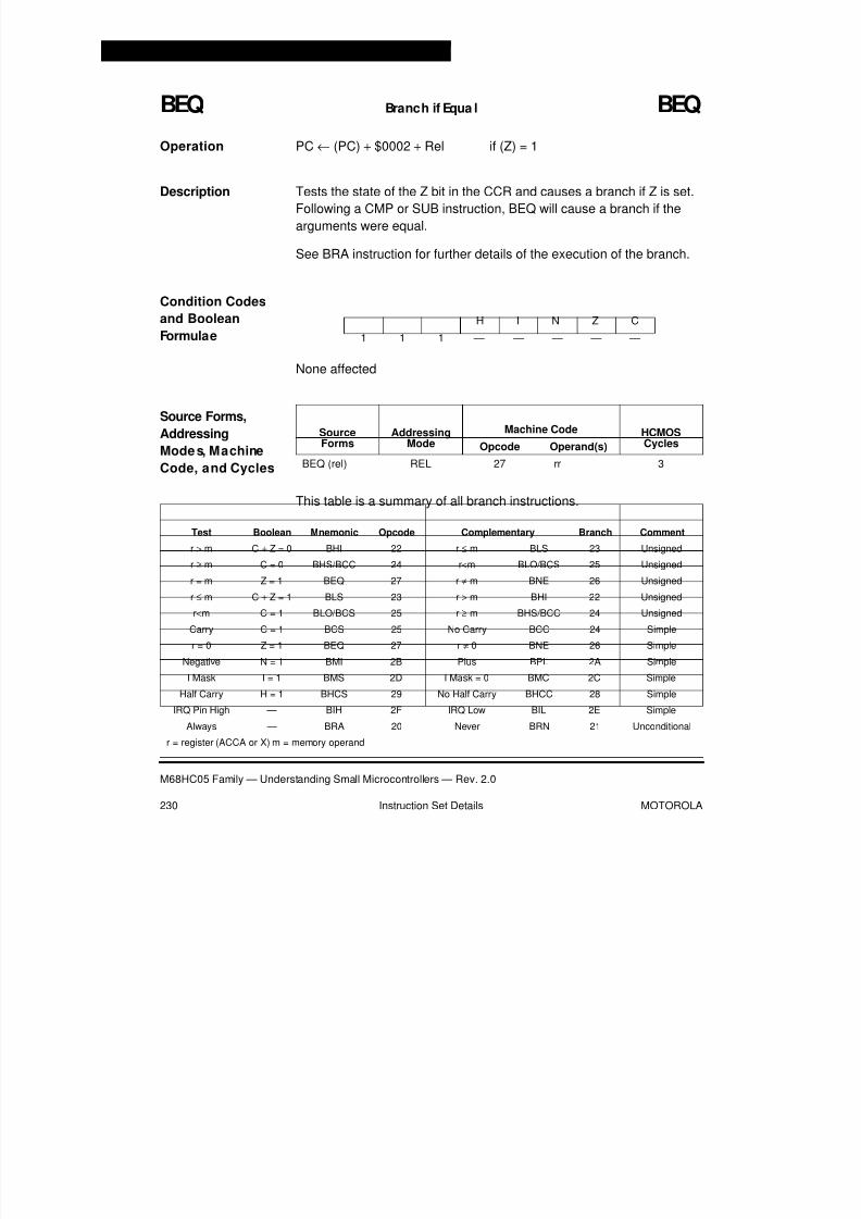
8/2/2019 122 Textbook
http://slidepdf.com/reader/full/122-textbook 230/331
Instruction Set Details
M68HC05 Family — Understanding Small Microcontrollers — Rev. 2.0
230 Instruction Set Details MOTOROLA
BEQ Branch if Equa l BEQ
Operation PC ← (PC) + $0002 + Rel if (Z) = 1
Description Tests the state of the Z bit in the CCR and causes a branch if Z is set.
Following a CMP or SUB instruction, BEQ will cause a branch if the
arguments were equal.
See BRA instruction for further details of the execution of the branch.
Condition Codes
and Boolean
Formulae
None affected
Source Forms,
Addressing
Mode s, Machine
Code, and Cycles
This table is a summary of all branch instructions.
H I N Z C
1 1 1 — — — — —
SourceForms
AddressingMode
Machine Code HCMOSCyclesOpcode Operand(s)
BEQ (rel) REL 27 rr 3
Test Boolean Mnemonic Opcode Complementary Branch Comment
r > m C + Z = 0 BHI 22 r ≤ m BLS 23 Unsigned
r ≥ m C = 0 BHS/BCC 24 r<m BLO/BCS 25 Unsigned
r = m Z = 1 BEQ 27 r ≠ m BNE 26 Unsigned
r ≤ m C + Z = 1 BLS 23 r > m BHI 22 Unsigned
r<m C = 1 BLO/BCS 25 r ≥ m BHS/BCC 24 Unsigned
Carry C = 1 BCS 25 No Carry BCC 24 Simple
r = 0 Z = 1 BEQ 27 r ≠ 0 BNE 26 Simple
Negative N = 1 BMI 2B Plus BPL 2A Simple
I Mask I = 1 BMS 2D I Mask = 0 BMC 2C Simple
Half Carry H = 1 BHCS 29 No Half Carry BHCC 28 Simple
IRQ Pin High — BIH 2F IRQ Low BIL 2E Simple
Always — BRA 20 Never BRN 21 Unconditional
r = register (ACCA or X) m = memory operand

8/2/2019 122 Textbook
http://slidepdf.com/reader/full/122-textbook 231/331
Instruction Set Details
M68HC05 Instruction Set
M68HC05 Family — Understanding Small Microcontrollers — Rev. 2.0
MOTOROLA Instruction Set Details 231
BHCC Branch if Half Ca rry Clea r BHCC
Operation PC ← (PC) + $0002 + Rel if (H) = 0
Description Tests the state of the H bit in the CCR and causes a branch if H is clear.
This instruction is used in algorithms involving BCD numbers.
See BRA instruction for further details of the execution of the branch.
Condition Codes
and Boolean
Formulae
None affected
Source Forms,
Addressing
Mode s, Machine
Code, and Cycles
This table is a summary of all branch instructions.
H I N Z C
1 1 1 — — — — —
SourceForms
AddressingMode
Machine Code HCMOSCyclesOpcode Operand(s)
BHCC (rel) REL 28 rr 3
Test Boolean Mnemonic Opcode Complementary Branch Comment
r > m C + Z = 0 BHI 22 r ≤ m BLS 23 Unsigned
r ≥ m C = 0 BHS/BCC 24 r<m BLO/BCS 25 Unsigned
r = m Z = 1 BEQ 27 r ≠ m BNE 26 Unsigned
r ≤ m C + Z = 1 BLS 23 r > m BHI 22 Unsigned
r<m C = 1 BLO/BCS 25 r ≥ m BHS/BCC 24 Unsigned
Carry C = 1 BCS 25 No Carry BCC 24 Simple
r = 0 Z = 1 BEQ 27 r ≠ 0 BNE 26 Simple
Negative N = 1 BMI 2B Plus BPL 2A Simple
I Mask I = 1 BMS 2D I Mask = 0 BMC 2C Simple
Half Carry H = 1 BHCS 29 No Half Carry BHCC 28 Simple
IRQ Pin High — BIH 2F IRQ Low BIL 2E Simple
Always — BRA 20 Never BRN 21 Unconditional
r = register (ACCA or X) m = memory operand

8/2/2019 122 Textbook
http://slidepdf.com/reader/full/122-textbook 232/331
Instruction Set Details
M68HC05 Family — Understanding Small Microcontrollers — Rev. 2.0
232 Instruction Set Details MOTOROLA
BHCS Branch if Half Carry Set BHCS
Operation PC ← (PC) + $0002 + Rel if (H) = 1
Description Tests the state of the H bit in the CCR and causes a branch if H is set.
This instruction is used in algorithms involving BCD numbers. See BRA
instruction for further details of the execution of the branch.
Condition Codes
and Boolean
Formulae
None affected
Source Forms,
Addressing
Mode s, Machine
Code, and Cycles
This table is a summary of all branch instructions.
H I N Z C
1 1 1 — — — — —
SourceForms
AddressingMode
Machine Code HCMOSCyclesOpcode Operand(s)
BHCS (rel) REL 29 rr 3
Test Boolean Mnemonic Opcode Complementary Branch Comment
r > m C + Z = 0 BHI 22 r ≤ m BLS 23 Unsigned
r ≥ m C = 0 BHS/BCC 24 r<m BLO/BCS 25 Unsigned
r = m Z = 1 BEQ 27 r ≠ m BNE 26 Unsigned
r ≤ m C + Z = 1 BLS 23 r > m BHI 22 Unsigned
r<m C = 1 BLO/BCS 25 r ≥ m BHS/BCC 24 Unsigned
Carry C = 1 BCS 25 No Carry BCC 24 Simple
r = 0 Z = 1 BEQ 27 r ≠ 0 BNE 26 Simple
Negative N = 1 BMI 2B Plus BPL 2A Simple
I Mask I = 1 BMS 2D I Mask = 0 BMC 2C Simple
Half Carry H = 1 BHCS 29 No Half Carry BHCC 28 Simple
IRQ Pin High — BIH 2F IRQ Low BIL 2E Simple
Always — BRA 20 Never BRN 21 Unconditional
r = register (ACCA or X) m = memory operand

8/2/2019 122 Textbook
http://slidepdf.com/reader/full/122-textbook 233/331
Instruction Set Details
M68HC05 Instruction Set
M68HC05 Family — Understanding Small Microcontrollers — Rev. 2.0
MOTOROLA Instruction Set Details 233
BHI Branch if Higher BHI
Operation C ← (PC) + $0002 + Rel if (C) + (Z) = 0
for instance, if (ACCA) > (M) (unsigned binary numbers)
Description Causes a branch if both C and Z are cleared. If the BHl instruction is
executed immediately after execution of a CMP or SUB instruction, the
branch will occur if the unsigned binary number in ACCA was greater
than the unsigned binary number in M.
See BRA instruction for further details of the execution of the branch.
Condition Codes
and BooleanFormulae
None affected
Source Forms,
Addressing
Mode s, Machine
Code, and Cycles
This table is a summary of all branch instructions.
H I N Z C
1 1 1 — — — — —
SourceForms
AddressingMode
Machine Code HCMOSCyclesOpcode Operand(s)
BHI (rel) REL 22 rr 3
Test Boolean Mnemonic Opcode Complementary Branch Comment
r > m C + Z = 0 BHI 22 r ≤ m BLS 23 Unsigned
r ≥ m C = 0 BHS/BCC 24 r<m BLO/BCS 25 Unsigned
r = m Z = 1 BEQ 27 r ≠ m BNE 26 Unsigned
r ≤ m C + Z = 1 BLS 23 r > m BHI 22 Unsigned
r<m C = 1 BLO/BCS 25 r ≥ m BHS/BCC 24 Unsigned
Carry C = 1 BCS 25 No Carry BCC 24 Simple
r = 0 Z = 1 BEQ 27 r ≠ 0 BNE 26 Simple
Negative N = 1 BMI 2B Plus BPL 2A SimpleI Mask I = 1 BMS 2D I Mask = 0 BMC 2C Simple
Half Carry H = 1 BHCS 29 No Half Carry BHCC 28 Simple
IRQ Pin High — BIH 2F IRQ Low BIL 2E Simple
Always — BRA 20 Never BRN 21 Unconditional
r = register (ACCA or X) m = memory operand

8/2/2019 122 Textbook
http://slidepdf.com/reader/full/122-textbook 234/331
Instruction Set Details
M68HC05 Family — Understanding Small Microcontrollers — Rev. 2.0
234 Instruction Set Details MOTOROLA
BHS Branch if Higher or Same BHS(Same asBCC)
Operation PC ← (PC) + $0002 + Rel if (C) = 0for instance, if (ACCA) ≥ (M) (unsigned binary numbers)
Description If the BHS instruction is executed immediately after execution of a CMP
or SUB instruction, the branch will occur if the unsigned binary number
in ACCA was greater than or equal to the unsigned binary number in M.
See BRA instruction for further details of the execution of the branch.
Condition Codes
and BooleanFormulae
None affected
Source Forms,
Addressing
Mode s, Machine
Code, and Cycles
This table is a summary of all branch instructions.
H I N Z C1 1 1 — — — — —
SourceForms
AddressingMode
Machine Code HCMOSCyclesOpcode Operand(s)
BHS (rel) REL 24 rr 3
Test Boolean Mnemonic Opcode Complementary Branch Comment
r > m C + Z = 0 BHI 22 r ≤ m BLS 23 Unsigned
r ≥ m C = 0 BHS/BCC 24 r<m BLO/BCS 25 Unsigned
r = m Z = 1 BEQ 27 r ≠ m BNE 26 Unsigned
r ≤ m C + Z = 1 BLS 23 r > m BHI 22 Unsigned
r<m C = 1 BLO/BCS 25 r ≥ m BHS/BCC 24 Unsigned
Carry C = 1 BCS 25 No Carry BCC 24 Simple
r = 0 Z = 1 BEQ 27 r ≠ 0 BNE 26 Simple
Negative N = 1 BMI 2B Plus BPL 2A Simple
I Mask I = 1 BMS 2D I Mask = 0 BMC 2C Simple
Half Carry H = 1 BHCS 29 No Half Carry BHCC 28 Simple
IRQ Pin High — BIH 2F IRQ Low BIL 2E Simple
Always — BRA 20 Never BRN 21 Unconditional
r = register (ACCA or X) m = memory operand
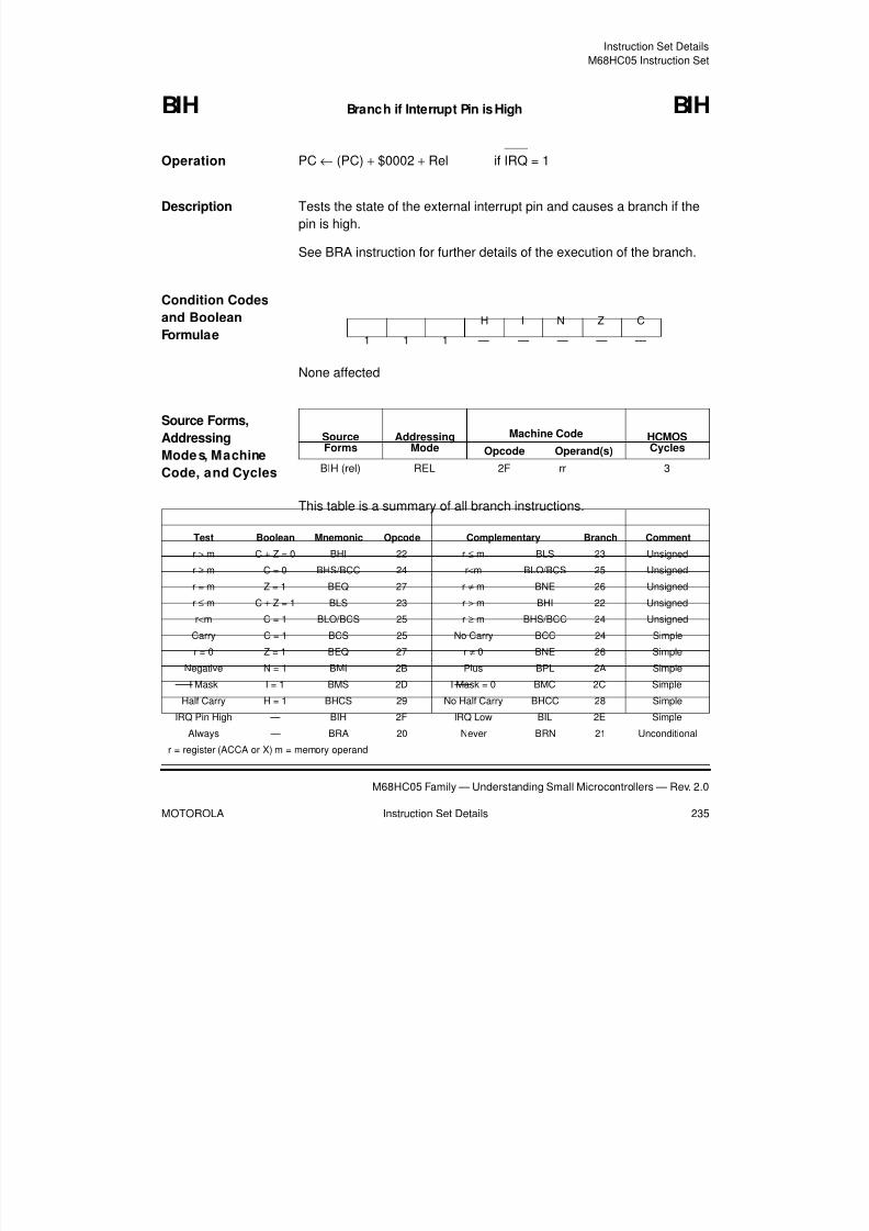
8/2/2019 122 Textbook
http://slidepdf.com/reader/full/122-textbook 235/331
Instruction Set Details
M68HC05 Instruction Set
M68HC05 Family — Understanding Small Microcontrollers — Rev. 2.0
MOTOROLA Instruction Set Details 235
BIH Branch if Interrupt Pin is High BIH
Operation PC ← (PC) + $0002 + Rel if IRQ = 1
Description Tests the state of the external interrupt pin and causes a branch if the
pin is high.
See BRA instruction for further details of the execution of the branch.
Condition Codes
and Boolean
Formulae
None affected
Source Forms,
Addressing
Mode s, Machine
Code, and Cycles
This table is a summary of all branch instructions.
H I N Z C
1 1 1 — — — — —
SourceForms
AddressingMode
Machine Code HCMOSCyclesOpcode Operand(s)
BIH (rel) REL 2F rr 3
Test Boolean Mnemonic Opcode Complementary Branch Comment
r > m C + Z = 0 BHI 22 r ≤ m BLS 23 Unsigned
r ≥ m C = 0 BHS/BCC 24 r<m BLO/BCS 25 Unsigned
r = m Z = 1 BEQ 27 r ≠ m BNE 26 Unsigned
r ≤ m C + Z = 1 BLS 23 r > m BHI 22 Unsigned
r<m C = 1 BLO/BCS 25 r ≥ m BHS/BCC 24 Unsigned
Carry C = 1 BCS 25 No Carry BCC 24 Simple
r = 0 Z = 1 BEQ 27 r ≠ 0 BNE 26 Simple
Negative N = 1 BMI 2B Plus BPL 2A Simple
I Mask I = 1 BMS 2D I Mask = 0 BMC 2C Simple
Half Carry H = 1 BHCS 29 No Half Carry BHCC 28 Simple
IRQ Pin High — BIH 2F IRQ Low BIL 2E Simple
Always — BRA 20 Never BRN 21 Unconditional
r = register (ACCA or X) m = memory operand

8/2/2019 122 Textbook
http://slidepdf.com/reader/full/122-textbook 236/331
Instruction Set Details
M68HC05 Family — Understanding Small Microcontrollers — Rev. 2.0
236 Instruction Set Details MOTOROLA
BIL Branch if Interrupt Pin is Low BIL
Operation PC ← (PC) + $0002 + Rel if IRQ = 0
Description Tests the state of the external interrupt pin and causes a branch if the
pin is low.
See BRA instruction for further details of the execution of the branch.
Condition Codes
and Boolean
Formulae
None affected
Source Forms,
Addressing
Mode s, Machine
Code, and Cycles
This table is a summary of all branch instructions.
H I N Z C
1 1 1 — — — — —
SourceForms
AddressingMode
Machine Code HCMOSCyclesOpcode Operand(s)
BIL (rel) REL 2E rr 3
Test Boolean Mnemonic Opcode Complementary Branch Comment
r > m C + Z = 0 BHI 22 r ≤ m BLS 23 Unsigned
r ≥ m C = 0 BHS/BCC 24 r<m BLO/BCS 25 Unsigned
r = m Z = 1 BEQ 27 r ≠ m BNE 26 Unsigned
r ≤ m C + Z = 1 BLS 23 r > m BHI 22 Unsigned
r<m C = 1 BLO/BCS 25 r ≥ m BHS/BCC 24 Unsigned
Carry C = 1 BCS 25 No Carry BCC 24 Simple
r = 0 Z = 1 BEQ 27 r ≠ 0 BNE 26 Simple
Negative N = 1 BMI 2B Plus BPL 2A Simple
I Mask I = 1 BMS 2D I Mask = 0 BMC 2C Simple
Half Carry H = 1 BHCS 29 No Half Carry BHCC 28 Simple
IRQ Pin High — BIH 2F IRQ Low BIL 2E Simple
Always — BRA 20 Never BRN 21 Unconditional
r = register (ACCA or X) m = memory operand

8/2/2019 122 Textbook
http://slidepdf.com/reader/full/122-textbook 237/331
Instruction Set Details
M68HC05 Instruction Set
M68HC05 Family — Understanding Small Microcontrollers — Rev. 2.0
MOTOROLA Instruction Set Details 237
BIT Bit Test Memory with Accumulator BIT
Operation (ACCA) • (M)
Description Performs the logical AND comparison of the contents of ACCA and the
contents of M and modifies the condition codes accordingly. Neither the
contents of ACCA nor M are altered. (Each bit of the result of the AND
would be the logical AND of the corresponding bits of ACCA and M).
Condition Codes
and Boolean
Formulae
N R7
Set if MSB of result is set; cleared otherwise.
Z R7 • R6 • R5 • R4 • R3 • R2 • R1 • R0
Set if result is $00; cleared otherwise.
Source Forms,
AddressingMode s, Machine
Code, and Cycles
H I N Z C1 1 1 — — ¤ ¤ —
SourceForms
AddressingMode
Machine Code HCMOSCyclesOpcode Operand(s)
BIT (opr) IMM A5 ii 2
BIT (opr) DIR B5 dd 3
BIT (opr) EXT C5 hh ll 4
BIT,X IX F5 3
BIT (opr),X IX1 E5 ff 4
BIT (opr),X IX2 D5 ee ff 5

8/2/2019 122 Textbook
http://slidepdf.com/reader/full/122-textbook 238/331
Instruction Set Details
M68HC05 Family — Understanding Small Microcontrollers — Rev. 2.0
238 Instruction Set Details MOTOROLA
BLO Branch if Lower BLO(Same asBCS)
Operation PC ← (PC) + $0002 + Rel if (C) = 1for instance, if (ACCA) < (M) (unsigned binary numbers)
Description If the BLO instruction is executed immediately after execution of a CMP
or SUB instruction, the branch will occur if the unsigned binary number
in ACCA was less than the unsigned binary number in M.
See BRA instruction for further details of the execution of the branch.
Condition Codes
and Boolean
Formulae
None affected
Source Forms,
Addressing
Mode s, Machine
Code, and Cycles
This table is a summary of all branch instructions.
H I N Z C
1 1 1 — — — — —
SourceForms
AddressingMode
Machine Code HCMOSCyclesOpcode Operand(s)
BLO (rel) REL 25 rr 3
Test Boolean Mnemonic Opcode Complementary Branch Comment
r > m C + Z = 0 BHI 22 r ≤ m BLS 23 Unsigned
r ≥ m C = 0 BHS/BCC 24 r<m BLO/BCS 25 Unsigned
r = m Z = 1 BEQ 27 r ≠ m BNE 26 Unsigned
r ≤ m C + Z = 1 BLS 23 r > m BHI 22 Unsigned
r<m C = 1 BLO/BCS 25 r ≥ m BHS/BCC 24 Unsigned
Carry C = 1 BCS 25 No Carry BCC 24 Simple
r = 0 Z = 1 BEQ 27 r ≠ 0 BNE 26 Simple
Negative N = 1 BMI 2B Plus BPL 2A Simple
I Mask I = 1 BMS 2D I Mask = 0 BMC 2C Simple
Half Carry H = 1 BHCS 29 No Half Carry BHCC 28 Simple
IRQ Pin High — BIH 2F IRQ Low BIL 2E Simple
Always — BRA 20 Never BRN 21 Unconditional
r = register (ACCA or X) m = memory operand

8/2/2019 122 Textbook
http://slidepdf.com/reader/full/122-textbook 239/331
Instruction Set Details
M68HC05 Instruction Set
M68HC05 Family — Understanding Small Microcontrollers — Rev. 2.0
MOTOROLA Instruction Set Details 239
BLS Branch if Lower or Same BLS
Operation PC ← (PC) + $0002 + Rel if [(C) + (Z)] = 1
for instance, if (ACCA) ≤ (M) (unsigned binary numbers)
Description Causes a branch if C is set or Z is set. If the BLS instruction is executed
immediately after execution of a CMP or SUB instruction, the branch will
occur if the unsigned binary number in ACCA was less than or equal to
the unsigned binary number in M.
See BRA instruction for further details of the execution of the branch.
Condition Codes
and BooleanFormulae
None affected
Source Forms,
Addressing
Mode s, Machine
Code, and Cycles
This table is a summary of all branch instructions.
H I N Z C1 1 1 — — — — —
SourceForms
AddressingMode
Machine Code HCMOSCyclesOpcode Operand(s)
BLS (rel) REL 23 rr 3
Test Boolean Mnemonic Opcode Complementary Branch Comment
r > m C + Z = 0 BHI 22 r ≤ m BLS 23 Unsigned
r ≥ m C = 0 BHS/BCC 24 r<m BLO/BCS 25 Unsigned
r = m Z = 1 BEQ 27 r ≠ m BNE 26 Unsigned
r ≤ m C + Z = 1 BLS 23 r > m BHI 22 Unsigned
r<m C = 1 BLO/BCS 25 r ≥ m BHS/BCC 24 Unsigned
Carry C = 1 BCS 25 No Carry BCC 24 Simple
r = 0 Z = 1 BEQ 27 r ≠ 0 BNE 26 Simple
Negative N = 1 BMI 2B Plus BPL 2A SimpleI Mask I = 1 BMS 2D I Mask = 0 BMC 2C Simple
Half Carry H = 1 BHCS 29 No Half Carry BHCC 28 Simple
IRQ Pin High — BIH 2F IRQ Low BIL 2E Simple
Always — BRA 20 Never BRN 21 Unconditional
r = register (ACCA or X) m = memory operand

8/2/2019 122 Textbook
http://slidepdf.com/reader/full/122-textbook 240/331
Instruction Set Details
M68HC05 Family — Understanding Small Microcontrollers — Rev. 2.0
240 Instruction Set Details MOTOROLA
BMC Branch if Interrupt Mask is Clear BMC
Operation PC ← (PC) + $0002 + Rel if I = 0
Description Tests the state of the I bit in the CCR and causes a branch if I is clear
(for instance., if interrupts are enabled). See BRA instruction for further
details of the execution of the branch.
Condition Codes
and Boolean
Formulae
None affected
Source Forms,
Addressing
Mode s, Machine
Code, and Cycles
This table is a summary of all branch instructions.
H I N Z C
1 1 1 — — — — —
SourceForms
AddressingMode
Machine Code HCMOSCyclesOpcode Operand(s)
BMC (rel) REL 2C rr 3
Test Boolean Mnemonic Opcode Complementary Branch Comment
r > m C + Z = 0 BHI 22 r ≤ m BLS 23 Unsigned
r ≥ m C = 0 BHS/BCC 24 r<m BLO/BCS 25 Unsigned
r = m Z = 1 BEQ 27 r ≠ m BNE 26 Unsigned
r ≤ m C + Z = 1 BLS 23 r > m BHI 22 Unsigned
r<m C = 1 BLO/BCS 25 r ≥ m BHS/BCC 24 Unsigned
Carry C = 1 BCS 25 No Carry BCC 24 Simple
r = 0 Z = 1 BEQ 27 r ≠ 0 BNE 26 Simple
Negative N = 1 BMI 2B Plus BPL 2A SimpleI Mask I = 1 BMS 2D I Mask = 0 BMC 2C Simple
Half Carry H = 1 BHCS 29 No Half Carry BHCC 28 Simple
IRQ Pin High — BIH 2F IRQ Low BIL 2E Simple
Always — BRA 20 Never BRN 21 Unconditional
r = register (ACCA or X) m = memory operand
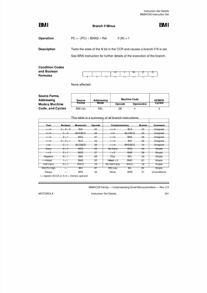
8/2/2019 122 Textbook
http://slidepdf.com/reader/full/122-textbook 241/331
Instruction Set Details
M68HC05 Instruction Set
M68HC05 Family — Understanding Small Microcontrollers — Rev. 2.0
MOTOROLA Instruction Set Details 241
BMI Branch if Minus BMI
Operation PC ← (PC) + $0002 + Rel if (N) = 1
Description Tests the state of the N bit in the CCR and causes a branch if N is set.
See BRA instruction for further details of the execution of the branch.
Condition Codes
and Boolean
Formulae
None affected
Source Forms,
Addressing
Mode s, Machine
Code, and Cycles
This table is a summary of all branch instructions.
H I N Z C
1 1 1 — — — — —
SourceForms
AddressingMode
Machine Code HCMOSCyclesOpcode Operand(s)
BMI (rel) REL 2B rr 3
Test Boolean Mnemonic Opcode Complementary Branch Comment
r > m C + Z = 0 BHI 22 r ≤ m BLS 23 Unsigned
r ≥ m C = 0 BHS/BCC 24 r<m BLO/BCS 25 Unsigned
r = m Z = 1 BEQ 27 r ≠ m BNE 26 Unsigned
r ≤ m C + Z = 1 BLS 23 r > m BHI 22 Unsigned
r<m C = 1 BLO/BCS 25 r ≥ m BHS/BCC 24 Unsigned
Carry C = 1 BCS 25 No Carry BCC 24 Simple
r = 0 Z = 1 BEQ 27 r ≠ 0 BNE 26 Simple
Negative N = 1 BMI 2B Plus BPL 2A Simple
I Mask I = 1 BMS 2D I Mask = 0 BMC 2C Simple
Half Carry H = 1 BHCS 29 No Half Carry BHCC 28 Simple
IRQ Pin High — BIH 2F IRQ Low BIL 2E Simple
Always — BRA 20 Never BRN 21 Unconditional
r = register (ACCA or X) m = memory operand

8/2/2019 122 Textbook
http://slidepdf.com/reader/full/122-textbook 242/331
Instruction Set Details
M68HC05 Family — Understanding Small Microcontrollers — Rev. 2.0
242 Instruction Set Details MOTOROLA
BMS Branch if Interrupt Mask is Set BMS
Operation PC ← (PC) + $0002 + Rel if (I) = 1
Description Tests the state of the I bit in the CCR and causes a branch if I is set (for
instance., if interrupts are disabled).
See BRA instruction for further details of the execution of the branch.
Condition Codes
and Boolean
Formulae
None affected
Source Forms,
Addressing
Mode s, Machine
Code, and Cycles
This table is a summary of all branch instructions.
H I N Z C
1 1 1 — — — — —
SourceForms
AddressingMode
Machine Code HCMOSCyclesOpcode Operand(s)
BMS (rel) REL 2D rr 3
Test Boolean Mnemonic Opcode Complementary Branch Comment
r > m C + Z = 0 BHI 22 r ≤ m BLS 23 Unsigned
r ≥ m C = 0 BHS/BCC 24 r<m BLO/BCS 25 Unsigned
r = m Z = 1 BEQ 27 r ≠ m BNE 26 Unsigned
r ≤ m C + Z = 1 BLS 23 r > m BHI 22 Unsigned
r<m C = 1 BLO/BCS 25 r ≥ m BHS/BCC 24 Unsigned
Carry C = 1 BCS 25 No Carry BCC 24 Simple
r = 0 Z = 1 BEQ 27 r ≠ 0 BNE 26 Simple
Negative N = 1 BMI 2B Plus BPL 2A Simple
I Mask I = 1 BMS 2D I Mask = 0 BMC 2C Simple
Half Carry H = 1 BHCS 29 No Half Carry BHCC 28 Simple
IRQ Pin High — BIH 2F IRQ Low BIL 2E Simple
Always — BRA 20 Never BRN 21 Unconditional
r = register (ACCA or X) m = memory operand

8/2/2019 122 Textbook
http://slidepdf.com/reader/full/122-textbook 243/331
Instruction Set Details
M68HC05 Instruction Set
M68HC05 Family — Understanding Small Microcontrollers — Rev. 2.0
MOTOROLA Instruction Set Details 243
BNE Branch if Not Equal BNE
Operation PC ← (PC) + $0002 + Rel if (Z) = 0
Description Tests the state of the Z bit in the CCR and causes a branch if Z is clear.
Following a compare or subtract instruction, BEQ will cause a branch if
the arguments were not equal.
See BRA instruction for further details of the execution of the branch.
Condition Codes
and Boolean
Formulae
None affected
Source Forms,
Addressing
Mode s, Machine
Code, and Cycles
This table is a summary of all branch instructions.
H I N Z C
1 1 1 — — — — —
SourceForms
AddressingMode
Machine Code HCMOSCyclesOpcode Operand(s)
BNE (rel) REL 26 rr 3
Test Boolean Mnemonic Opcode Complementary Branch Comment
r > m C + Z = 0 BHI 22 r ≤ m BLS 23 Unsigned
r ≥ m C = 0 BHS/BCC 24 r<m BLO/BCS 25 Unsigned
r = m Z = 1 BEQ 27 r ≠ m BNE 26 Unsigned
r ≤ m C + Z = 1 BLS 23 r > m BHI 22 Unsigned
r<m C = 1 BLO/BCS 25 r ≥ m BHS/BCC 24 Unsigned
Carry C = 1 BCS 25 No Carry BCC 24 Simple
r = 0 Z = 1 BEQ 27 r ≠ 0 BNE 26 Simple
Negative N = 1 BMI 2B Plus BPL 2A Simple
I Mask I = 1 BMS 2D I Mask = 0 BMC 2C Simple
Half Carry H = 1 BHCS 29 No Half Carry BHCC 28 Simple
IRQ Pin High — BIH 2F IRQ Low BIL 2E Simple
Always — BRA 20 Never BRN 21 Unconditional
r = register (ACCA or X) m = memory operand
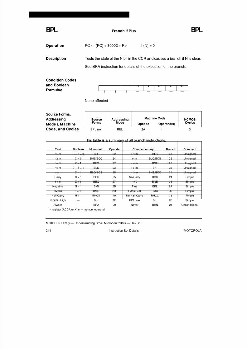
8/2/2019 122 Textbook
http://slidepdf.com/reader/full/122-textbook 244/331
Instruction Set Details
M68HC05 Family — Understanding Small Microcontrollers — Rev. 2.0
244 Instruction Set Details MOTOROLA
BPL Branch if Plus BPL
Operation PC ← (PC) + $0002 + Rel if (N) = 0
Description Tests the state of the N bit in the CCR and causes a branch if N is clear.
See BRA instruction for details of the execution of the branch.
Condition Codes
and Boolean
Formulae
None affected
Source Forms,
Addressing
Mode s, Machine
Code, and Cycles
This table is a summary of all branch instructions.
H I N Z C
1 1 1 — — — — —
SourceForms
AddressingMode
Machine Code HCMOSCyclesOpcode Operand(s)
BPL (rel) REL 2A rr 3
Test Boolean Mnemonic Opcode Complementary Branch Comment
r > m C + Z = 0 BHI 22 r ≤ m BLS 23 Unsigned
r ≥ m C = 0 BHS/BCC 24 r<m BLO/BCS 25 Unsigned
r = m Z = 1 BEQ 27 r ≠ m BNE 26 Unsigned
r ≤ m C + Z = 1 BLS 23 r > m BHI 22 Unsigned
r<m C = 1 BLO/BCS 25 r ≥ m BHS/BCC 24 Unsigned
Carry C = 1 BCS 25 No Carry BCC 24 Simple
r = 0 Z = 1 BEQ 27 r ≠ 0 BNE 26 Simple
Negative N = 1 BMI 2B Plus BPL 2A Simple
I Mask I = 1 BMS 2D I Mask = 0 BMC 2C Simple
Half Carry H = 1 BHCS 29 No Half Carry BHCC 28 Simple
IRQ Pin High — BIH 2F IRQ Low BIL 2E Simple
Always — BRA 20 Never BRN 21 Unconditional
r = register (ACCA or X) m = memory operand

8/2/2019 122 Textbook
http://slidepdf.com/reader/full/122-textbook 245/331
Instruction Set Details
M68HC05 Instruction Set
M68HC05 Family — Understanding Small Microcontrollers — Rev. 2.0
MOTOROLA Instruction Set Details 245
BRA Branch Always BRA
Operation PC ← (PC) + $0002 + Rel
Description Unconditional branch to the address given by the foregoing formula, in
which Rel is the relative offset stored as a twos-complement number in
the last byte of machine code corresponding to the branch instruction.
PC is the address of the opcode for the branch instruction.
The source program specifies the destination of any branch instruction
by its absolute address, either as a numerical value or as a symbol or
expression which can be numerically evaluated by the assembler. The
assembler calculates the relative address, Rel, from the absolute
address and the current value of the location counter.
Condition Codes
and Boolean
Formulae
None affected
Source Forms,
Addressing
Mode s, Machine
Code, and Cycles
This table is a summary of all branch instructions.
H I N Z C
1 1 1 — — — — —
SourceForms
AddressingMode
Machine Code HCMOSCyclesOpcode Operand(s)
BRA (rel) REL 20 rr 3
Test Boolean Mnemonic Opcode Complementary Branch Comment
r > m C + Z = 0 BHI 22 r ≤ m BLS 23 Unsigned
r ≥ m C = 0 BHS/BCC 24 r<m BLO/BCS 25 Unsigned
r = m Z = 1 BEQ 27 r ≠ m BNE 26 Unsigned
r ≤ m C + Z = 1 BLS 23 r > m BHI 22 Unsigned
r<m C = 1 BLO/BCS 25 r ≥ m BHS/BCC 24 Unsigned
Carry C = 1 BCS 25 No Carry BCC 24 Simple
r = 0 Z = 1 BEQ 27 r ≠ 0 BNE 26 Simple
Negative N = 1 BMI 2B Plus BPL 2A Simple
I Mask I = 1 BMS 2D I Mask = 0 BMC 2C Simple
Half Carry H = 1 BHCS 29 No Half Carry BHCC 28 Simple
IRQ Pin High — BIH 2F IRQ Low BIL 2E Simple
Always — BRA 20 Never BRN 21 Unconditional
r = register (ACCA or X) m = memory operand

8/2/2019 122 Textbook
http://slidepdf.com/reader/full/122-textbook 246/331
Instruction Set Details
M68HC05 Family — Understanding Small Microcontrollers — Rev. 2.0
246 Instruction Set Details MOTOROLA
BRCLR n Branch if Bit n is Clear BRCLRn
Operation PC ← (PC) + $0003 + Rel if bit n of M = 0
Description Tests bit n (n = 7, 6, 5. . . 0) of location M and branches if the bit is clear.
M can be any RAM or I/O register address in the $0000 to $00FF area
of memory (for instance, direct addressing mode is used to specify the
address of the operand).
The C bit is set to the state of the bit tested. When used along with an
appropriate rotate instruction, BRCLR n provides an easy method for
performing serial to parallel conversions.
Condition Codes
and Boolean
Formulae
C Set if Mn = 1; cleared otherwise.
Source Forms,
Addressing
Mode s, Machine
Code, and Cycles
H I N Z C
1 1 1 — — — — ¤
SourceForms
AddressingMode
Machine Code HCMOSCyclesOpcode Operand(s)
BRCLR 0,(opr),(rel) DIR (bit 0) 01 dd rr 5
BRCLR 1,(opr),(rel) DIR (bit 1) 03 dd rr 5
BRCLR 2,(opr),(rel) DIR (bit 2) 05 dd rr 5
BRCLR 3,(opr),(rel) DIR (bit 3) 07 dd rr 5
BRCLR 4,(opr),(rel) DIR (bit 4) 09 dd rr 5
BRCLR 5,(opr),(rel) DIR (bit 5) OB dd rr 5
BRCLR 6,(opr),(rel) DIR (bit 6) OD dd rr 5BRCLR 7,(opr),(rel) DIR (bit 7) OF dd rr 5

8/2/2019 122 Textbook
http://slidepdf.com/reader/full/122-textbook 247/331
Instruction Set Details
M68HC05 Instruction Set
M68HC05 Family — Understanding Small Microcontrollers — Rev. 2.0
MOTOROLA Instruction Set Details 247
BRN Branch Never BRN
Operation PC ← (PC) + $0002
Description Never branches. In effect, this instruction can be considered as a 2-byte
NOP (no operation) requiring three cycles for execution. Its inclusion in
the instruction set is to provide a complement for the BRA instruction.
The instruction is useful during program debug to negate the effect of
another branch instruction without disturbing the offset byte.
Condition Codes
and Boolean
Formulae
None affected
Source Forms,
Addressing
Mode s, Machine
Code, and Cycles
This table is a summary of all branch instructions.
H I N Z C
1 1 1 — — — — —
SourceForms
AddressingMode
Machine Code HCMOSCyclesOpcode Operand(s)
BRN (rel) REL 21 rr 3
Test Boolean Mnemonic Opcode Complementary Branch Comment
r > m C + Z = 0 BHI 22 r ≤ m BLS 23 Unsigned
r ≥ m C = 0 BHS/BCC 24 r<m BLO/BCS 25 Unsigned
r = m Z = 1 BEQ 27 r ≠ m BNE 26 Unsigned
r ≤ m C + Z = 1 BLS 23 r > m BHI 22 Unsigned
r<m C = 1 BLO/BCS 25 r ≥ m BHS/BCC 24 Unsigned
Carry C = 1 BCS 25 No Carry BCC 24 Simple
r = 0 Z = 1 BEQ 27 r ≠ 0 BNE 26 Simple
Negative N = 1 BMI 2B Plus BPL 2A SimpleI Mask I = 1 BMS 2D I Mask = 0 BMC 2C Simple
Half Carry H = 1 BHCS 29 No Half Carry BHCC 28 Simple
IRQ Pin High — BIH 2F IRQ Low BIL 2E Simple
Always — BRA 20 Never BRN 21 Unconditional
r = register (ACCA or X) m = memory operand

8/2/2019 122 Textbook
http://slidepdf.com/reader/full/122-textbook 248/331
Instruction Set Details
M68HC05 Family — Understanding Small Microcontrollers — Rev. 2.0
248 Instruction Set Details MOTOROLA
BRSET n Branch if Bit n is Set BRSETn
Operation PC ← (PC) + $0003 + Rel if bit n of M = 1
Description Tests bit n (n = 7, 6, 5, 0) of location M and branches if the bit is set. M
can be any RAM or I/O register address in the $0000 to $00FF area of
memory (for instance, direct addressing mode is used to specify the
address of the operand).
The C bit is set to the state of the bit tested. When used along with an
appropriate rotate instruction, BRSET n provides an easy method for
performing serial to parallel conversions.
Condition Codes
and Boolean
Formulae
C Set if Mn = 1; cleared otherwise.
Source Forms,
Addressing
Mode s, Machine
Code, and Cycles
H I N Z C
1 1 1 — — — — ¤
SourceForms
AddressingMode
Machine Code HCMOSCyclesOpcode Operand(s)
BRSET 0,(opr),(rel) DIR (bit 0) 00 dd rr 5
BRSET 1,(opr),(rel) DIR (bit 1) 02 dd rr 5
BRSET 2,(opr),(rel) DIR (bit 2) 04 dd rr 5
BRSET 3,(opr),(rel) DIR (bit 3) 06 dd rr 5
BRSET 4,(opr),(rel) DIR (bit 4) 08 dd rr 5
BRSET 5,(opr), (rel) DIR (bit 5) 0A dd rr 5
BRSET 6,(opr),(rel) DIR (bit 6) 0C dd rr 5BRSET 7,(opr),(rel) DIR (bit 7) 0E dd rr 5
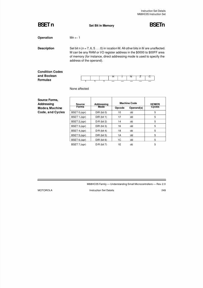
8/2/2019 122 Textbook
http://slidepdf.com/reader/full/122-textbook 249/331
Instruction Set Details
M68HC05 Instruction Set
M68HC05 Family — Understanding Small Microcontrollers — Rev. 2.0
MOTOROLA Instruction Set Details 249
BSET n Set Bit in Memory BSETn
Operation Mn ← 1
Description Set bit n (n = 7, 6, 5 . . . 0) in location M. All other bits in M are unaffected.
M can be any RAM or I/O register address in the $0000 to $00FF area
of memory (for instance, direct addressing mode is used to specify the
address of the operand).
Condition Codes
and Boolean
Formulae
None affected
Source Forms,
Addressing
Mode s, Machine
Code, and Cycles
H I N Z C1 1 1 — — — — —
SourceForms
AddressingMode
Machine Code HCMOSCyclesOpcode Operand(s)
BSET 0,(opr) DIR (bit 0) 10 dd 5
BSET 1,(opr) DIR (bit 1) 12 dd 5
BSET 2,(opr) DIR (bit 2) 14 dd 5
BSET 3,(opr) DIR (bit 3) 16 dd 5
BSET 4,(opr) DIR (bit 4) 18 dd 5
BSET 5,(opr) DIR (bit 5) 1A dd 5
BSET 6,(opr) DIR (bit 6) 1C dd 5
BSET 7,(opr) DIR (bit 7) 1E dd 5

8/2/2019 122 Textbook
http://slidepdf.com/reader/full/122-textbook 250/331
Instruction Set Details
M68HC05 Family — Understanding Small Microcontrollers — Rev. 2.0
250 Instruction Set Details MOTOROLA
BSR Branch to Subroutine BSR
Operation PC ← (PC) + $0002 Advance PC to return address↓ (PCL); SP ← (SP)–$0001 Push low-order return onto stack↓ (PCL); SP ← (SP)–$0001 Push high-order return onto stackPC ← (PC) + Rel Load PC with start address of
requested subroutine
Description The program counter is incremented by two from the opcode address,
for instance, so it points to the opcode of the next instruction which will
be the return address. The least significant byte of the contents of the
program counter (low-order return address) is pushed onto the stack.
The stack pointer is then decremented by one. The most significant byte
of the contents of the program counter (high-order return address) is
pushed onto the stack. The stack pointer is then decremented by one. A
branch then occurs to the location specified by the branch offset.
See BRA instruction for further details of the execution of the branch.
Condition Codes
and Boolean
Formulae
None affected
Source Forms,
Addressing
Mode s, Machine
Code, and Cycles
H I N Z C
1 1 1 — — — — —
SourceForms
AddressingMode
Machine Code HCMOSCyclesOpcode Operand(s)
BSR (rel) REL AD rr 6

8/2/2019 122 Textbook
http://slidepdf.com/reader/full/122-textbook 251/331
Instruction Set Details
M68HC05 Instruction Set
M68HC05 Family — Understanding Small Microcontrollers — Rev. 2.0
MOTOROLA Instruction Set Details 251
CLC Clear Carry Bit CLC
Operation C bit ← 0
Description Clears the C bit in the CCR. CLC may be used to set up the C bit prior
to a shift or rotate instruction involving the C bit.
Condition Codes
and Boolean
Formulae
C 0
Cleared
Source Forms,
Addressing
Mode s, Machine
Code, and Cycles
H I N Z C
1 1 1 — — — — 0
SourceForms
AddressingMode
Machine Code HCMOSCyclesOpcode Operand(s)
CLC INH 98 2
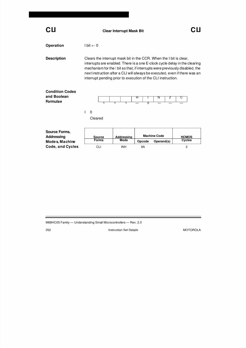
8/2/2019 122 Textbook
http://slidepdf.com/reader/full/122-textbook 252/331
Instruction Set Details
M68HC05 Family — Understanding Small Microcontrollers — Rev. 2.0
252 Instruction Set Details MOTOROLA
CLI Clear Interrupt Mask Bit CLI
Operation I bit ← 0
Description Clears the interrupt mask bit in the CCR. When the I bit is clear,
interrupts are enabled. There is a one E-clock cycle delay in the clearing
mechanism for the I bit so that, if interrupts were previously disabled, the
next instruction after a CLI will always be executed, even if there was an
interrupt pending prior to execution of the CLI instruction.
Condition Codes
and Boolean
Formulae
I 0
Cleared
Source Forms,
Addressing
Mode s, MachineCode, and Cycles
H I N Z C
1 1 1 — 0 — — —
Source
Forms
Addressing
Mode
Machine Code HCMOS
CyclesOpcode Operand(s)
CLI INH 9A 2

8/2/2019 122 Textbook
http://slidepdf.com/reader/full/122-textbook 253/331
Instruction Set Details
M68HC05 Instruction Set
M68HC05 Family — Understanding Small Microcontrollers — Rev. 2.0
MOTOROLA Instruction Set Details 253
CLR Clear CLR
Operation ACCA ← $00 or: M ← $00 or: X ← $00
Description The contents of ACCA, M, or X are replaced with 0s.
Condition Codes
and Boolean
Formulae
I 0Cleared
Z 1
Set
Source Forms,
Addressing
Mode s, Machine
Code, and Cycles
H I N Z C
1 1 1 — — 0 1 —
SourceForms
AddressingMode
Machine Code HCMOSCyclesOpcode Operand(s)
CLRA INH (A) 4F 3
CLRX INH (X) 5F 3
CLR (opr) DIR 3F dd 5
CLR ,X IX 7F 5
CLR (opr),X IX1 6F ff 6

8/2/2019 122 Textbook
http://slidepdf.com/reader/full/122-textbook 254/331
Instruction Set Details
M68HC05 Family — Understanding Small Microcontrollers — Rev. 2.0
254 Instruction Set Details MOTOROLA
CMP Compare Accumulator with Memory CMP
Operation (ACCA) – (M)
Description Compares the contents of ACCA to the contents of M and sets the
condition codes, which may be used for arithmetic and logical
conditional branching. The contents of both ACCA and M are
unchanged.
Condition Codes
and Boolean
Formulae
N R7
Set if MSB of result is set; cleared otherwise.
Z R7 • R6 • R5 • R4 • R3 • R2 • R1 • R0
Set if all bits of the result are cleared; cleared otherwise.
C A7 • M7 + M7 • R7 + R7 • A7
Set if absolute value of the contents of memory is larger than the ab-
solute value of the accumulator; cleared otherwise.
Source Forms,
Addressing
Mode s, Machine
Code, and Cycles
H I N Z C1 1 1 — — ¤ ¤ ¤
SourceForms
AddressingMode
Machine Code HCMOSCyclesOpcode Operand(s)
CMP (opr) IMM A1 ii 2
CMP (opr) DIR B1 dd 3
CMP (opr) EXT C1 hh ll 4
CMP ,X IX F1 3
CMP (opr),X IX1 E1 ff 4
CMP (opr),X IX2 D1 ee ff 5
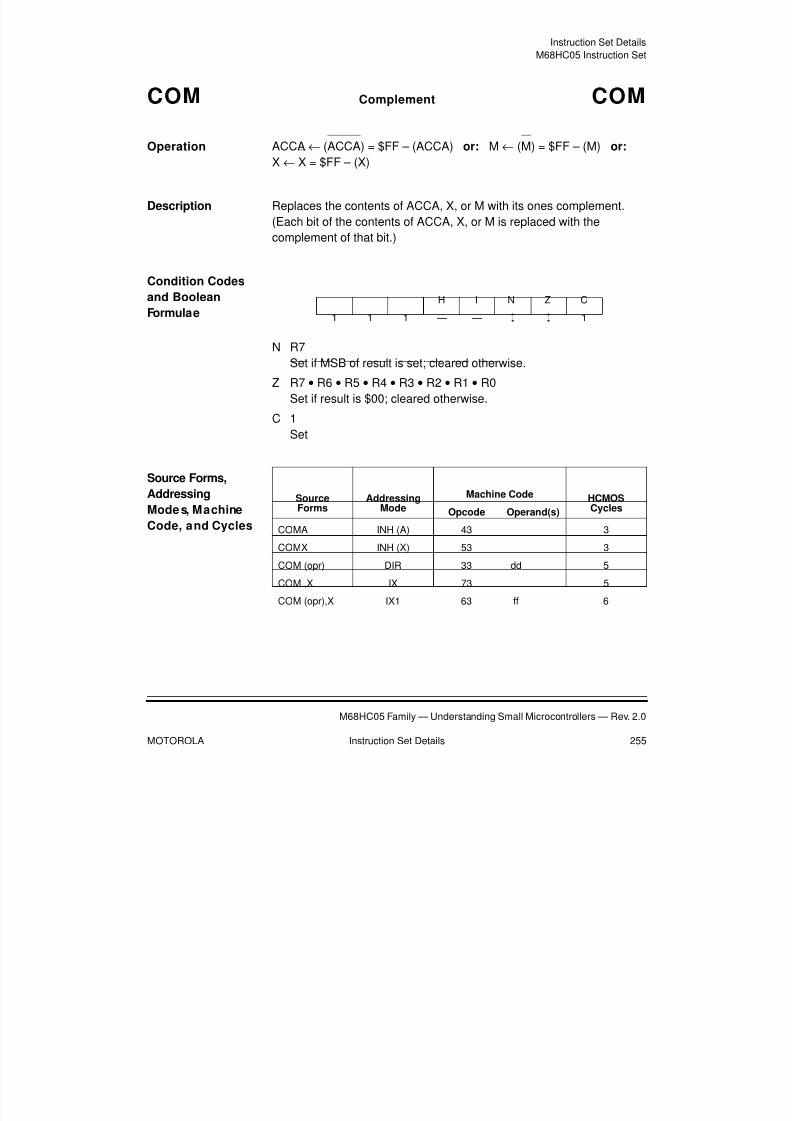
8/2/2019 122 Textbook
http://slidepdf.com/reader/full/122-textbook 255/331
Instruction Set Details
M68HC05 Instruction Set
M68HC05 Family — Understanding Small Microcontrollers — Rev. 2.0
MOTOROLA Instruction Set Details 255
COM Complement COM
Operation ACCA ← (ACCA) = $FF – (ACCA) or: M ← (M) = $FF – (M) or:X ← X = $FF – (X)
Description Replaces the contents of ACCA, X, or M with its ones complement.
(Each bit of the contents of ACCA, X, or M is replaced with the
complement of that bit.)
Condition Codes
and BooleanFormulae
N R7
Set if MSB of result is set; cleared otherwise.
Z R7 • R6 • R5 • R4 • R3 • R2 • R1 • R0
Set if result is $00; cleared otherwise.
C 1
Set
Source Forms,
Addressing
Mode s, Machine
Code, and Cycles
H I N Z C1 1 1 — — ¤ ¤ 1
SourceForms
AddressingMode
Machine Code HCMOSCyclesOpcode Operand(s)
COMA INH (A) 43 3
COMX INH (X) 53 3
COM (opr) DIR 33 dd 5
COM ,X IX 73 5
COM (opr),X IX1 63 ff 6

8/2/2019 122 Textbook
http://slidepdf.com/reader/full/122-textbook 256/331
Instruction Set Details
M68HC05 Family — Understanding Small Microcontrollers — Rev. 2.0
256 Instruction Set Details MOTOROLA
CPX Compare Index Register with Memory CPX
Operation (X) – (M)
Description Compares the contents of the index register with the contents of memory
and sets the condition codes, which may be used for arithmetic and
logical branching. The contents of both ACCA and M are unchanged.
Condition Codes
and Boolean
Formulae
N R7
Set if MSB of result is set; cleared otherwise.
Z R7 • R6 • R5 • R4 • R3 • R2 • R1 • R0
Set if result is $00; cleared otherwise.
C IX7 • M7 + M7 • R7 + R7 • IX7
Set if the absolute value of the contents of memory is larger than the
absolute value of the index register; cleared otherwise.
Source Forms,
Addressing
Mode s, Machine
Code, and Cycles
H I N Z C
1 1 1 — — ¤ ¤ ¤
SourceForms
AddressingMode
Machine Code HCMOSCyclesOpcode Operand(s)
I CPX (opr) IMM A3 ii 2
CPX (opr) DIR B3 dd 3
CPX (opr) EXT C3 hh ll 4
CPX,X IX F3 3
CPX (opr),X IX1 E3 ff 4
CPX (opr),X IX2 D3 ee ff 5

8/2/2019 122 Textbook
http://slidepdf.com/reader/full/122-textbook 257/331
Instruction Set Details
M68HC05 Instruction Set
M68HC05 Family — Understanding Small Microcontrollers — Rev. 2.0
MOTOROLA Instruction Set Details 257
DEC Decrement DEC
Operation ACCA ← (ACCA) – $01 or: M ← (M) – $01 or: X ← (X)-$01
Description Subtract one from the contents of ACCA, X, or M.
The N and Z bits in the CCR are set or cleared according to the result of
this operation. The C bit in the CCR is not affected; therefore, the only
branch instructions that are useful following a DEC instruction are BEQ,
BNE, BPL, and BMI.
Condition Codesand Boolean
Formulae
N R7
Set if MSB of result is set; cleared otherwise.
Z R7 • R6 • R5 • R4 • R3 • R2 • R1 • R0
Set if result is $00; cleared otherwise.
Source Forms,
Addressing Modes
Machine Code,
and Cycles
H I N Z C
1 1 1 — — ¤ ¤ —
SourceForms
AddressingMode
Machine Code HCMOSCyclesOpcode Operand(s)
DECA INH (A) 4A 3
DECX INH (X) 5A 3
DEC (opr) DIR 3A dd 5
DEC ,X IX 7A 5
DEC (opr),X IX1 6A ff 6
DEX is recognized by the assembler as being equivalent to DECX.

8/2/2019 122 Textbook
http://slidepdf.com/reader/full/122-textbook 258/331
Instruction Set Details
M68HC05 Family — Understanding Small Microcontrollers — Rev. 2.0
258 Instruction Set Details MOTOROLA
EOR Exclusive-OR Memory with Accumulator EOR
Operation ACCA ← (ACCA) ⊕ (M)
Description Performs the logical exclusive-OR between the contents of ACCA and
the contents of M and places the result in ACCA. (Each bit of ACCA after
the operation will be the logical exclusive-OR of the corresponding bits
of M and ACCA before the operation.)
Condition Codes
and Boolean
Formulae
N R7
Set if MSB of result is set; cleared otherwise.
Z R7 • R6 • R5 • R4 • R3 • R2 • R1 • R0
Set if result is $00; cleared otherwise.
Source Forms,
AddressingMode s, Machine
Code, and Cycles
H I N Z C1 1 1 — — ¤ ¤ —
SourceForms
AddressingMode
Machine Code HCMOSCyclesOpcode Operand(s)
EOR (opr) IMM A8 ii 2
EOR (opr) DIR B8 dd 3
EOR (opr) EXT C8 hh ll 4
EOR ,X IX F8 3
EOR (opr),X IX1 E8 ff 4
EOR (opr),X IX2 D8 ee ff 5
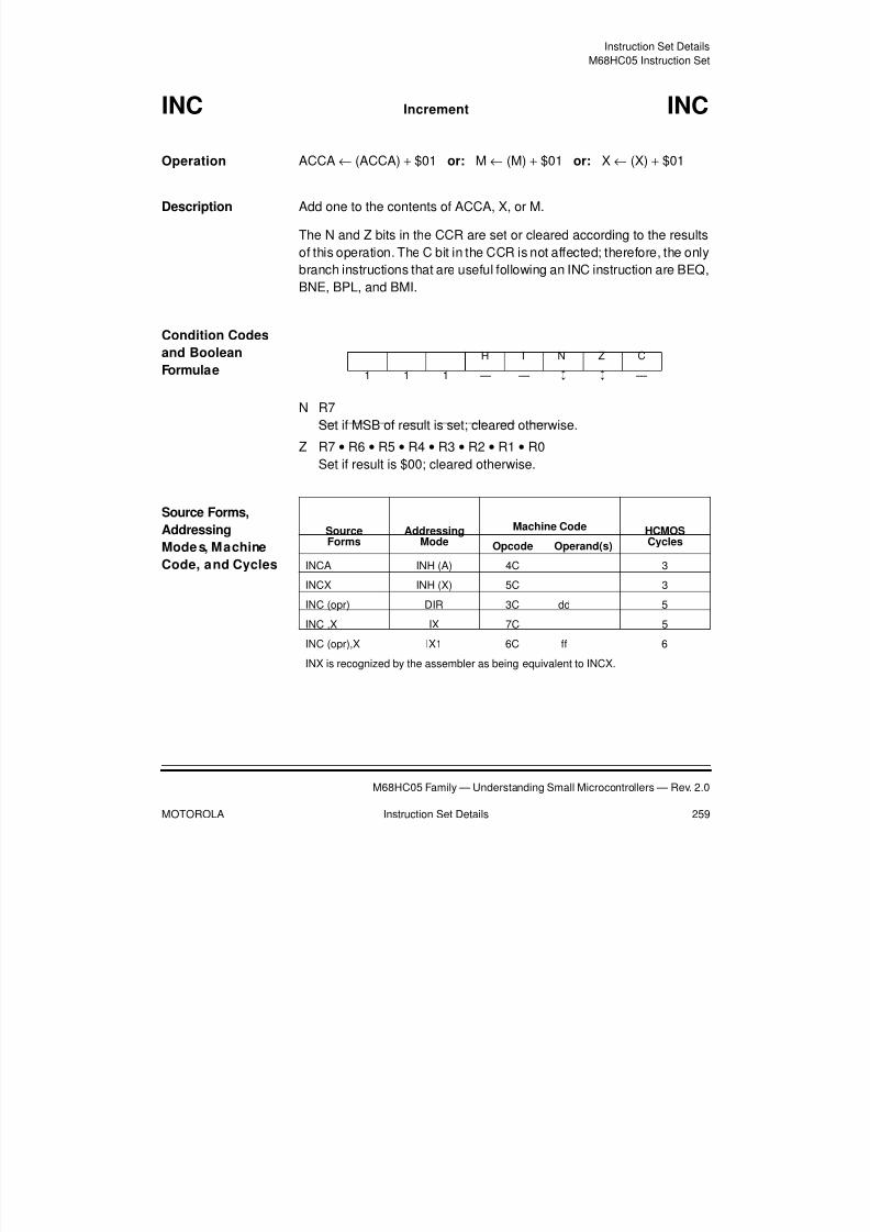
8/2/2019 122 Textbook
http://slidepdf.com/reader/full/122-textbook 259/331
Instruction Set Details
M68HC05 Instruction Set
M68HC05 Family — Understanding Small Microcontrollers — Rev. 2.0
MOTOROLA Instruction Set Details 259
INC Increment INC
Operation ACCA ← (ACCA) + $01 or: M ← (M) + $01 or: X ← (X) + $01
Description Add one to the contents of ACCA, X, or M.
The N and Z bits in the CCR are set or cleared according to the results
of this operation. The C bit in the CCR is not affected; therefore, the only
branch instructions that are useful following an INC instruction are BEQ,
BNE, BPL, and BMI.
Condition Codesand Boolean
Formulae
N R7
Set if MSB of result is set; cleared otherwise.
Z R7 • R6 • R5 • R4 • R3 • R2 • R1 • R0
Set if result is $00; cleared otherwise.
Source Forms,
Addressing
Mode s, Machine
Code, and Cycles
H I N Z C
1 1 1 — — ¤ ¤ —
SourceForms
AddressingMode
Machine Code HCMOSCyclesOpcode Operand(s)
INCA INH (A) 4C 3
INCX INH (X) 5C 3
INC (opr) DIR 3C dd 5
INC ,X IX 7C 5
INC (opr),X IX1 6C ff 6
INX is recognized by the assembler as being equivalent to INCX.

8/2/2019 122 Textbook
http://slidepdf.com/reader/full/122-textbook 260/331
Instruction Set Details
M68HC05 Family — Understanding Small Microcontrollers — Rev. 2.0
260 Instruction Set Details MOTOROLA
JMP Jump JMP
Operation PC ← Effective Address
Description A jump occurs to the instruction stored at the effective address. The
effective address is obtained according to the rules for EXTended,
DIRect, or INDexed addressing.
Condition Codes
and Boolean
Formulae
None affected
Source Forms,
Addressing
Mode s, Machine
Code, and Cycles
H I N Z C
1 1 1 — — — — —
SourceForms
AddressingMode
Machine Code HCMOSCyclesOpcode Operand(s)
JMP (opr) DIR BC dd 2
JMP (opr) EXT CC hh ll 3
JMP ,X IX FC 2
JMP (opr), X IX1 EC ff 3
JMP (opr),X IX2 DC ee ff 4

8/2/2019 122 Textbook
http://slidepdf.com/reader/full/122-textbook 261/331
Instruction Set Details
M68HC05 Instruction Set
M68HC05 Family — Understanding Small Microcontrollers — Rev. 2.0
MOTOROLA Instruction Set Details 261
JSR Jump to Subroutine JSR
Operation PC ← (PC) + n n = 1, 2, 3 depending on address mode↓ (PCL); SP ← SP – $0001 Push low-order return address onto stack
↓ (PCH); SP ← SP – $0001 Push high-order return address onto
stack
PC ← Effective Addr Load PC with start address of
requested subroutine
Description The program counter is incremented by n so that it points to the opcode
of the instruction that follows the JSR instruction (n = 1, 2, or 3
depending on the addressing mode). The PC is then pushed onto thestack, eight bits at a time, least significant byte first. Unused bits in the
program counter high byte are stored as ones on the stack. The stack
pointer points to the next empty location on the stack. A jump occurs to
the instruction stored at the effective address. The effective address is
obtained according to the rules for EXTended, DIRect, or INDexed
addressing.
Condition Codes
and BooleanFormulae
None affected
Source Forms,
Addressing
Mode s, Machine
Code, and Cycles
H I N Z C
1 1 1 — — — — —
SourceForms
AddressingMode
Machine Code HCMOSCyclesOpcode Operand(s)
JSR (opr) DIR BD dd 5
JSR (opr) EXT CD hh ll 6
JSR ,X IX FD 5
JSR (opr), X IX1 ED ff 6
JSR (opr),X IX2 DD ee ff 7

8/2/2019 122 Textbook
http://slidepdf.com/reader/full/122-textbook 262/331
Instruction Set Details
M68HC05 Family — Understanding Small Microcontrollers — Rev. 2.0
262 Instruction Set Details MOTOROLA
LDA Load Accumulator from Memory LDA
Operation ACCA ← (M)
Description Loads the contents of memory into the accumulator. The condition
codes are set according to the data.
Condition Codes
and Boolean
Formulae
N R7
Set if MSB of result is set; cleared otherwise.
Z R7 • R6 • R5 • R4 • R3 • R2 • R1 • R0
Set if result is $00; cleared otherwise.
Source Forms,
Addressing
Mode s, Machine
Code, and Cycles
H I N Z C
1 1 1 — — ¤ ¤ —
SourceForms
AddressingMode
Machine Code HCMOSCyclesOpcode Operand(s)
LDA (opr) IMM A6 ii 2
LDA (opr) DIR B6 dd 3
LDA (opr) EXT C6 hh ll 4
LDA ,X IX F6 3
LDA (opr),X IX1 E6 ff 4
LDA (opr),X IX2 D6 ee ff 5

8/2/2019 122 Textbook
http://slidepdf.com/reader/full/122-textbook 263/331
Instruction Set Details
M68HC05 Instruction Set
M68HC05 Family — Understanding Small Microcontrollers — Rev. 2.0
MOTOROLA Instruction Set Details 263
LDX Load Index Register from Me mory LDX
Operation X ← (M)
Description Loads the contents of the specified memory location into the index
register. The condition codes are set according to the data.
Condition Codes
and Boolean
Formulae
N R7
Set if MSB of result is set; cleared otherwise.
Z R7 • R6 • R5 • R4 • R3 • R2 • R1 • R0
Set if result is $00; cleared otherwise.
Source Forms,
Addressing
Mode s, Machine
Code, and Cycles
H I N Z C
1 1 1 — — ¤ ¤ —
SourceForms
AddressingMode
Machine Code HCMOSCyclesOpcode Operand(s)
LDX (opr) IMM AE ii 2
LDX (opr) DIR BE dd 3
LDX (opr) EXT CE hh ll 4
LDX ,X IX FE 3
LDX (opr),X IX1 EE ff 4
LDX (opr),X IX2 DE ee ff 5

8/2/2019 122 Textbook
http://slidepdf.com/reader/full/122-textbook 264/331
Instruction Set Details
M68HC05 Family — Understanding Small Microcontrollers — Rev. 2.0
264 Instruction Set Details MOTOROLA
LSL Logical Shift Left LSL(Same asASL)
Operation
Description Shifts all bits of the ACCA, X, or M one place to the left. Bit 0 is loaded
with 0. The C bit in the CCR is loaded from the most significant bit of
ACCA, X, or M.
Condition Codes
and BooleanFormulae
N R7
Set if MSB of result is set; cleared otherwise.
Z R7 • R6 • R5 • R4 • R3 • R2 • R1 • R0
Set if result is $00; cleared otherwise.
C b7
Set if, before the shift, the MSB of ACCA or M was set; cleared oth-
erwise.
Source Forms,
Addressing
Mode s, Machine
Code, and Cycles
C b7 – – – – – – b0 0
H I N Z C1 1 1 — — ¤ ¤ ¤
SourceForms
AddressingMode
Machine Code HCMOSCyclesOpcode Operand(s)
LSLA INH (A) 48 3
LSLX INH (X) 58 3
LSL (opr) DIR 38 dd 5
LSL ,X IX 78 5
LSL (opr),X IX1 68 ff 6

8/2/2019 122 Textbook
http://slidepdf.com/reader/full/122-textbook 265/331
Instruction Set Details
M68HC05 Instruction Set
M68HC05 Family — Understanding Small Microcontrollers — Rev. 2.0
MOTOROLA Instruction Set Details 265
LSR Logical Shift Right LSR
Operation
Description Shifts all bits of ACCA, X, or M one place to the right. Bit 7 is loaded with
0. Bit 0 is shifted into the C bit.
Condition Codes
and Boolean
Formulae
N 0
Cleared.
Z R7 • R6 • R5 • R4 • R3 • R2 • R1 • R0
Set if result is $00; cleared otherwise.
C b0
Set if, before the shift, the LSB of ACCA, X, or M was set; cleared oth-
erwise.
Source Forms,
Addressing
Mode s, Machine
Code, and Cycles
Cb7 – – – – – – b00
H I N Z C
1 1 1 — — 0 ¤ ¤
SourceForms
AddressingMode
Machine Code HCMOSCyclesOpcode Operand(s)
LSRA INH (A) 44 3
LSRX INH (X) 54 3
LSR (opr) DIR 34 dd 5
LSR ,X IX 74 5
LSR (opr),X IX1 64 ff 6

8/2/2019 122 Textbook
http://slidepdf.com/reader/full/122-textbook 266/331
Instruction Set Details
M68HC05 Family — Understanding Small Microcontrollers — Rev. 2.0
266 Instruction Set Details MOTOROLA
MUL Multiply Unsigned MUL
Operation X:A ← X x A
Description Multiplies the eight bits in the index register by the eight bits in the
accumulator to obtain a 16-bit unsigned number in the concatenated
index register and accumulator. After the operation, X contains the upper
8 bits of the 16-bit result.
Condition Codes
and Boolean
Formulae
H 0
Cleared
C 0
Cleared
Source Forms,
AddressingMode s, Machine
Code, and Cycles
H I N Z C1 1 1 0 — — — 0
SourceForms
AddressingMode
Machine Code HCMOSCyclesOpcode Operand(s)
MUL INH 42 11

8/2/2019 122 Textbook
http://slidepdf.com/reader/full/122-textbook 267/331
Instruction Set Details
M68HC05 Instruction Set
M68HC05 Family — Understanding Small Microcontrollers — Rev. 2.0
MOTOROLA Instruction Set Details 267
NEG Negate NEG
Operation ACCA ← – (ACCA); or: X ← – (X); or: M ← – (M)
Description Replaces the contents of ACCA, X, or M with its twos complement. Note
that the value $80 is left unchanged.
Condition Codes
and Boolean
Formulae
N R7
Set if MSB of result is set; cleared otherwise.
Z R7 • R6 • R5 • R4 • R3 • R2 • R1 • R0
Set if result is $00; cleared otherwise.
C R7 + R6 + R5 + R4 + R3 + R2 + R1 + R0
Set if there is a borrow in the implied subtraction from 0; cleared oth-
erwise. The C bit will be set in all cases except when the contents of
ACCA, X, or M (prior to the NEG operation) is $00.
Source Forms,
Addressing
Mode s, Machine
Code, and Cycles
H I N Z C
1 1 1 — — ¤ ¤ ¤
SourceForms
AddressingMode
Machine Code HCMOSCyclesOpcode Operand(s)
NEGA INH (A) 40 3
NEGX INH (X) 50 3
NEG (opr) DIR 30 dd 5
NEG ,X IX 70 5
NEG (opr),X IX1 60 ff 6
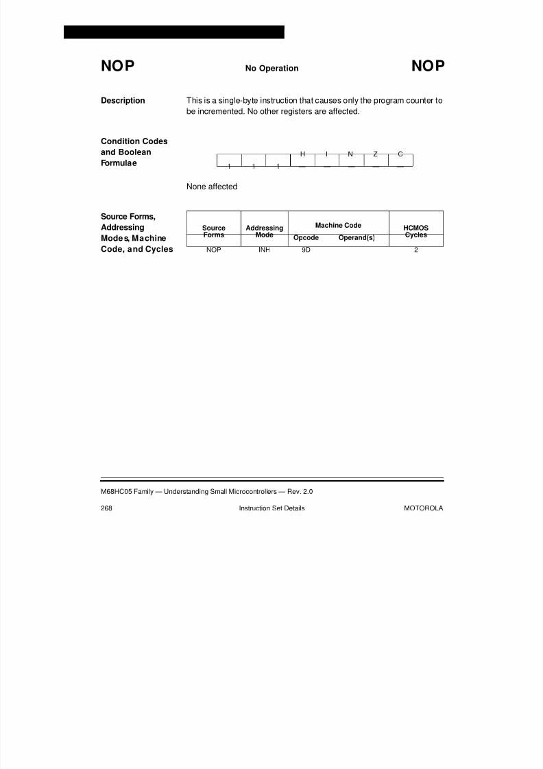
8/2/2019 122 Textbook
http://slidepdf.com/reader/full/122-textbook 268/331
Instruction Set Details
M68HC05 Family — Understanding Small Microcontrollers — Rev. 2.0
268 Instruction Set Details MOTOROLA
NOP No Operation NOP
Description This is a single-byte instruction that causes only the program counter tobe incremented. No other registers are affected.
Condition Codes
and Boolean
Formulae
None affected
Source Forms,
Addressing
Mode s, Machine
Code, and Cycles
H I N Z C
1 1 1 — — — — —
SourceForms
AddressingMode
Machine Code HCMOSCyclesOpcode Operand(s)
NOP INH 9D 2

8/2/2019 122 Textbook
http://slidepdf.com/reader/full/122-textbook 269/331
Instruction Set Details
M68HC05 Instruction Set
M68HC05 Family — Understanding Small Microcontrollers — Rev. 2.0
MOTOROLA Instruction Set Details 269
ORA Inclusive-OR ORA
Operation ACCA ← (ACCA) + (M)
Description Performs the logical inclusive-OR between the contents of ACCA and
the contents of M and places the result in ACCA. Each bit of ACCA after
the operation will be the logical inclusive-OR of the corresponding bits of
M and of ACCA before the operation.
Condition Codes
and Boolean
Formulae
N R7
Set if MSB of result is set; cleared otherwise.
Z R7 • R6 • R5 • R4 • R3 • R2 • R1 • R0
Set if result is $00; cleared otherwise.
Source Forms,
AddressingMode s, Machine
Code, and Cycles
H I N Z C1 1 1 — — ¤ ¤ —
SourceForms
AddressingMode
Machine Code HCMOSCyclesOpcode Operand(s)
ORA (opr) IMM AA ii 2
ORA (opr) DIR BA dd 3
ORA (opr) EXT CA hh ll 4
ORA ,X IX FA 3
ORA (opr),X IX1 EA ff 4
ORA (opr),X 1X2 DA ee ff 5
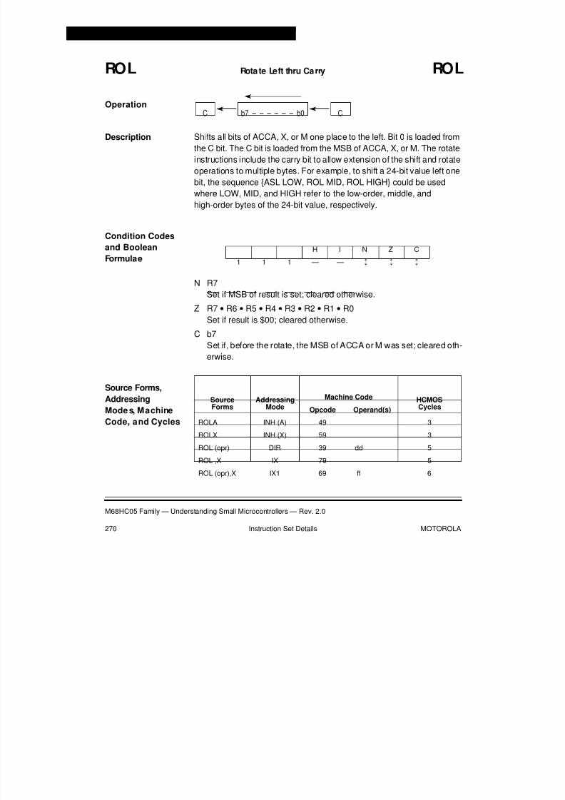
8/2/2019 122 Textbook
http://slidepdf.com/reader/full/122-textbook 270/331
Instruction Set Details
M68HC05 Family — Understanding Small Microcontrollers — Rev. 2.0
270 Instruction Set Details MOTOROLA
ROL Rotate Left thru Carry ROL
Operation
Description Shifts all bits of ACCA, X, or M one place to the left. Bit 0 is loaded from
the C bit. The C bit is loaded from the MSB of ACCA, X, or M. The rotate
instructions include the carry bit to allow extension of the shift and rotate
operations to multiple bytes. For example, to shift a 24-bit value left one
bit, the sequence ASL LOW, ROL MID, ROL HIGH could be used
where LOW, MID, and HIGH refer to the low-order, middle, and
high-order bytes of the 24-bit value, respectively.
Condition Codes
and Boolean
Formulae
N R7
Set if MSB of result is set; cleared otherwise.
Z R7 • R6 • R5 • R4 • R3 • R2 • R1 • R0
Set if result is $00; cleared otherwise.C b7
Set if, before the rotate, the MSB of ACCA or M was set; cleared oth-
erwise.
Source Forms,
Addressing
Mode s, Machine
Code, and Cycles
C b7 – – – – – – b0 C
H I N Z C
1 1 1 — — ¤ ¤ ¤
SourceForms
AddressingMode
Machine Code HCMOSCyclesOpcode Operand(s)
ROLA INH (A) 49 3
ROLX INH (X) 59 3
ROL (opr) DIR 39 dd 5
ROL ,X IX 79 5
ROL (opr),X IX1 69 ff 6

8/2/2019 122 Textbook
http://slidepdf.com/reader/full/122-textbook 271/331
Instruction Set Details
M68HC05 Instruction Set
M68HC05 Family — Understanding Small Microcontrollers — Rev. 2.0
MOTOROLA Instruction Set Details 271
ROR Rotate Right thru Carry ROR
Operation
Description Shift all bits of ACCA, X, or M one place to the right. Bit 7 is loaded from
the C bit. The rotate operations include the carry bit to allow extension
of the shift and rotate operations to multiple bytes. For example, to shift
a 24-bit value right one bit, the sequence LSR HIGH, ROR MID, ROR
LOW could be used where LOW, MID, and HIGH refer to the low-order,
middle, and high-order bytes of the 24-bit value, respectively.
Condition Codes
and Boolean
Formulae
N R7
Set if MSB of result is set; cleared otherwise.
Z R7 • R6 • R5 • R4 • R3 • R2 • R1 • R0
Set if all bits of the result are cleared; cleared otherwise.
C b0Set if, before the rotate, the LSB of ACCA, X, or M was set; cleared
otherwise.
Source Forms,
Addressing
Mode s, Machine
Code, and Cycles
Cb7 – – – – – – b0C
H I N Z C
1 1 1 — — ¤ ¤ ¤
SourceForms
AddressingMode
Machine Code HCMOSCyclesOpcode Operand(s)
RORA INH (A) 46 3
RORX INH (X) 56 3
ROR (opr) DIR 36 dd 5
ROR ,X IX 76 5
ROR (opr),X IX1 66 ff 6

8/2/2019 122 Textbook
http://slidepdf.com/reader/full/122-textbook 272/331
Instruction Set Details
M68HC05 Family — Understanding Small Microcontrollers — Rev. 2.0
272 Instruction Set Details MOTOROLA
RSP Reset Stack Pointer RSP
Operation SP ← $00FF
Description Resets the stack pointer to the top of the stack.
Condition Codes
and Boolean
Formulae
None affected
Source Forms,
Addressing
Mode s, Machine
Code, and Cycles
H I N Z C
1 1 1 — — — — —
SourceForms
AddressingMode
Machine Code HCMOSCyclesOpcode Operand(s)
RSP INH 9C 2

8/2/2019 122 Textbook
http://slidepdf.com/reader/full/122-textbook 273/331
Instruction Set Details
M68HC05 Instruction Set
M68HC05 Family — Understanding Small Microcontrollers — Rev. 2.0
MOTOROLA Instruction Set Details 273
RTI Return from Interrupt RTI
Operation SP ← (SP) + $0001; ↑ CCR Restore CCR from stackSP ← (SP) + $0001; ↑ ACCA Restore ACCA from stackSP ← (SP) + $0001; ↑ X Restore X from stackSP ← (SP) + $0001; ↑ PCH Restore PCH from stackSP ← (SP) + $0001; ↑ PCL Restore PCL from stack
Description The condition codes, accumulator, the index register, and the program
counter are restored to the state previously saved on the stack. The 1-bit
will be reset if the corresponding bit stored on the stack is 0.
Condition Codes
and Boolean
Formulae
Set or cleared according to the byte pulled from the stack.
Source Forms,
Addressing
Mode s, Machine
Code, and Cycles
H I N Z C
1 1 1 ¤ ¤ ¤ ¤ ¤
Source
Forms
Addressing
Mode
Machine Code HCMOS
CyclesOpcode Operand(s)
RTI INH 80 9

8/2/2019 122 Textbook
http://slidepdf.com/reader/full/122-textbook 274/331
Instruction Set Details
M68HC05 Family — Understanding Small Microcontrollers — Rev. 2.0
274 Instruction Set Details MOTOROLA
RTS Return from Subroutine RTS
Operation SP ← (SP) + $0001; ↑ PCH Restore PCH from stackSP ← (SP) + $0001; ↑ PCL Restore PCL from stack
Description The stack pointer is incremented by one. The contents of the byte of
memory that is pointed to by the stack pointer is loaded into the
high-order byte of the program counter. The stack pointer is again
incremented by one. The contents of the byte of memory at the address
now contained in the stack pointer is loaded into the low-order eight bits
of the program counter.
Condition Codes
and Boolean
Formulae
None affected
Source Forms,
AddressingMode s, Machine
Code, and Cycles
H I N Z C
1 1 1 — — — — —
SourceForms AddressingMode
Machine CodeHCMOSCyclesOpcode Operand(s)
RTS INH 81 6

8/2/2019 122 Textbook
http://slidepdf.com/reader/full/122-textbook 275/331
Instruction Set Details
M68HC05 Instruction Set
M68HC05 Family — Understanding Small Microcontrollers — Rev. 2.0
MOTOROLA Instruction Set Details 275
SBC Subtract with Carry SBC
Operation ACCA ← (ACCA) – (M) – (C)
Description Subtracts the contents of M and the contents of C from the contents of
ACCA and places the result in ACCA.
Condition Codes
and Boolean
Formulae
N R7
Set if MSB of result is set; cleared otherwise.
Z R7 • R6 • R5 • R4 • R3 • R2 • R1 • R0
Set if result is $00; cleared otherwise.
C A7 • M7 + M7 • R7 + R7 • A7
Set if absolute value of the contents of memory plus previous carry
is larger than the absolute value of the accumulator; cleared
otherwise.
Source Forms,
Addressing
Mode s, Machine
Code, and Cycles
H I N Z C
1 1 1 — — ¤ ¤ ¤
SourceForms
AddressingMode
Machine Code HCMOSCyclesOpcode Operand(s)
SBC (opr) IMM A2 ii 2
SBC (opr) DIR B2 dd 3
SBC (opr) EXT C2 hh ll 4
SBC ,X IX F2 3
SBC (opr),X IX1 E2 ff 4
SBC (opr),X IX2 D2 ee ff 5
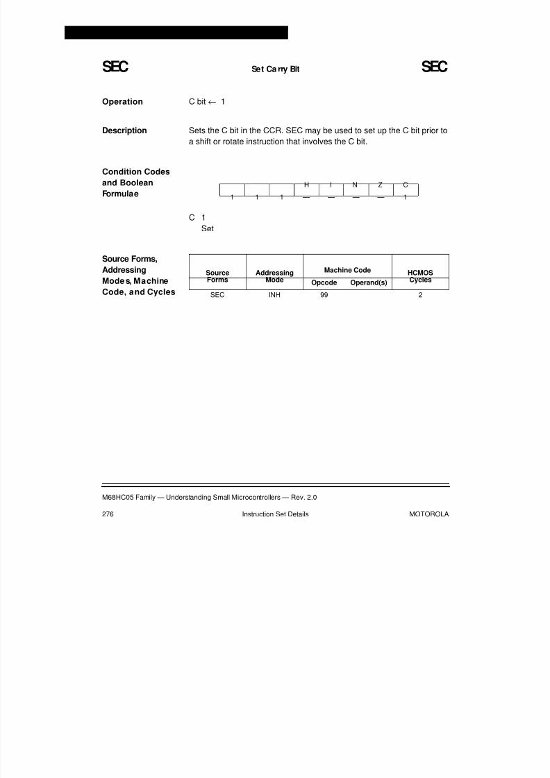
8/2/2019 122 Textbook
http://slidepdf.com/reader/full/122-textbook 276/331
Instruction Set Details
M68HC05 Family — Understanding Small Microcontrollers — Rev. 2.0
276 Instruction Set Details MOTOROLA
SEC Set Ca rry Bit SEC
Operation C bit ← 1
Description Sets the C bit in the CCR. SEC may be used to set up the C bit prior to
a shift or rotate instruction that involves the C bit.
Condition Codes
and Boolean
Formulae
C 1
Set
Source Forms,
Addressing
Mode s, Machine
Code, and Cycles
H I N Z C
1 1 1 — — — — 1
SourceForms
AddressingMode
Machine Code HCMOSCyclesOpcode Operand(s)
SEC INH 99 2

8/2/2019 122 Textbook
http://slidepdf.com/reader/full/122-textbook 277/331
Instruction Set Details
M68HC05 Instruction Set
M68HC05 Family — Understanding Small Microcontrollers — Rev. 2.0
MOTOROLA Instruction Set Details 277
SEI Set Interrupt Mask Bit SEI
Operation I bit ← 1
Description Sets the interrupt mask bit in the CCR. The microprocessor is inhibited
from servicing interrupts while the I bit is set.
Condition Codes
and Boolean
Formulae
I 1
Set
Source Forms,
Addressing
Mode s, Machine
Code, and Cycles
H I N Z C
1 1 1 — 1 — — —
SourceForms
AddressingMode
Machine Code HCMOSCyclesOpcode Operand(s)
SEI INH 9B 2

8/2/2019 122 Textbook
http://slidepdf.com/reader/full/122-textbook 278/331
Instruction Set Details
M68HC05 Family — Understanding Small Microcontrollers — Rev. 2.0
278 Instruction Set Details MOTOROLA
STA Store Accumulator in Memory STA
Operation M ← (ACCA)
Description Stores the contents of ACCA in memory. The contents of ACCA remain
unchanged.
Condition Codes
and Boolean
Formulae
N A7
Set if MSB of result is set; cleared otherwise.
Z A7 • A6 • A5 • A4 • A3 • A2 • A1 • A0
Set if result is $00; cleared otherwise.
Source Forms,
Addressing
Mode s, Machine
Code, and Cycles
H I N Z C
1 1 1 — — ¤ ¤ —
SourceForms
AddressingMode
Machine Code HCMOSCyclesOpcode Operand(s)
STA (opr) DIR B7 dd 4
STA (opr) EXT C7 hh ll 5
STA ,X IX F7 4
STA (opr),X IX1 E7 ff 5
STA (opr),X IX2 D7 ee ff 6

8/2/2019 122 Textbook
http://slidepdf.com/reader/full/122-textbook 279/331
Instruction Set Details
M68HC05 Instruction Set
M68HC05 Family — Understanding Small Microcontrollers — Rev. 2.0
MOTOROLA Instruction Set Details 279
STOP Enable IRQ, Stop Oscillator STOP
Description Reduces power consumption by eliminating all dynamic powerdissipation. This results in: 1) timer prescaler cleared, 2) timer interrupts
disabled, 3) timer interrupt flag cleared, 4) external interrupt request
enabled, and 5) oscillator inhibited.
When the RESET or IRQ input goes low, the oscillator is enabled, a
delay of 1920 processor clock cycles is initiated allowing the oscillator to
stabilize, the interrupt request vector or reset vector is fetched, and the
service routine is executed, depending on which signal was applied.
External interrupts are enabled following the STOP command.
Condition Codes
and Boolean
Formulae
I 0
Cleared
Source Forms,
Addressing
Mode s, Machine
Code, and Cycles
H I N Z C
1 1 1 — 0 — — —
SourceForms
AddressingMode
Machine Code HCMOSCyclesOpcode Operand(s)
STOP INH 8E 2

8/2/2019 122 Textbook
http://slidepdf.com/reader/full/122-textbook 280/331
Instruction Set Details
M68HC05 Family — Understanding Small Microcontrollers — Rev. 2.0
280 Instruction Set Details MOTOROLA
STX Store Index Register X in Memory STX
Operation M ← (X)
Description Stores the contents of X in memory. The contents of X remain
unchanged.
Condition Codes
and Boolean
Formulae
N X7
Set if MSB of result is set; cleared otherwise.
Z X7 • X6 • X5 • X4 • X3 • X2 • X1 • X0
Set if result is $00; cleared otherwise.
Source Forms,
Addressing
Mode s, Machine
Code, and Cycles
H I N Z C
1 1 1 — — ¤ ¤ —
SourceForms
AddressingMode
Machine Code HCMOSCyclesOpcode Operand(s)
STX (opr) DIR BF ii 4
STX (opr) EXT CF hh ii 5
STX ,X IX FF 4
STX (opr),X IX1 EF ff 5
STX (opr),X IX2 DF ee ff 6
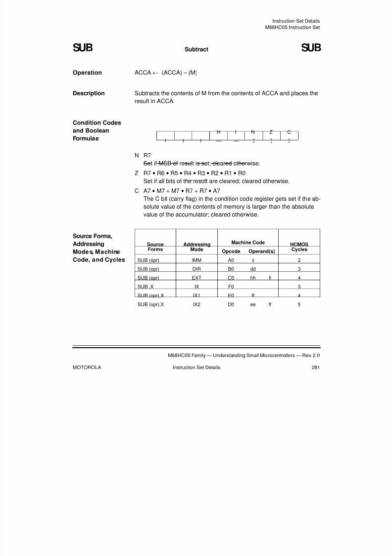
8/2/2019 122 Textbook
http://slidepdf.com/reader/full/122-textbook 281/331
Instruction Set Details
M68HC05 Instruction Set
M68HC05 Family — Understanding Small Microcontrollers — Rev. 2.0
MOTOROLA Instruction Set Details 281
SUB Subtract SUB
Operation ACCA ← (ACCA) – (M)
Description Subtracts the contents of M from the contents of ACCA and places the
result in ACCA.
Condition Codes
and Boolean
Formulae
N R7
Set if MSB of result is set; cleared otherwise.
Z R7 • R6 • R5 • R4 • R3 • R2 • R1 • R0
Set if all bits of the result are cleared; cleared otherwise.
C A7 • M7 + M7 • R7 + R7 • A7
The C bit (carry flag) in the condition code register gets set if the ab-
solute value of the contents of memory is larger than the absolute
value of the accumulator; cleared otherwise.
Source Forms,
Addressing
Mode s, Machine
Code, and Cycles
H I N Z C
1 1 1 — — ¤ ¤ ¤
SourceForms
AddressingMode
Machine Code HCMOSCyclesOpcode Operand(s)
SUB (opr) IMM A0 ii 2
SUB (opr) DIR B0 dd 3
SUB (opr) EXT C0 hh ll 4
SUB ,X IX F0 3
SUB (opr),X IX1 E0 ff 4
SUB (opr),X IX2 D0 ee ff 5

8/2/2019 122 Textbook
http://slidepdf.com/reader/full/122-textbook 282/331
Instruction Set Details
M68HC05 Family — Understanding Small Microcontrollers — Rev. 2.0
282 Instruction Set Details MOTOROLA
SWI Software Interrupt SWI
Operation PC ← (PC) + $0001 Advance PC to return address
↓ (PCL); SP ← (SP) – $0001 Push low-order return addressonto stack↓ (PCH); SP ← (SP) – $0001 Push high-order return address
onto stack↓ (X); SP ← (SP) – $0001 Push index register onto stack↓ (ACCA); SP ← (SP) – $0001 Push accumulator onto stack↓ (CCR); SP ← (SP) – $0001 Push CCR onto stackI bit ← 1PCH ← ($xFFC) Vector fetch (x = 1 or 3 depending onPCL ← ($xFFD) M68HC05 device)
Description The program counter is incremented by one. The program counter,index register, and accumulator are pushed onto the stack. The CCR
bits are then pushed onto the stack, with bits H, I, N, Z, and C going into
bit positions 4–0 and bit positions 7, 6, and 5 containing ones. The stack
pointer is decremented by one after each byte of data is stored on the
stack. The interrupt mask bit is then set. The program counter is then
loaded with the address stored in the SWI vector (located at memory
locations n–0002 and n–0003, where n is the address corresponding to
a high state on all lines of the address bus). The address of the SWI
vector can be expressed as $xFFC:$xFFD, where x is 1 or 3 depending
on the M68HC05 device being used. This instruction is not maskable by
the I bit.
Condition Codes
and Boolean
Formulae
I 1
Set
Source Forms,
Addressing
Mode s, Machine
Code, and Cycles
H I N Z C
1 1 1 — 1 — — —
SourceForms
AddressingMode
Machine Code HCMOSCyclesOpcode Operand(s)
SWI INH 83 10

8/2/2019 122 Textbook
http://slidepdf.com/reader/full/122-textbook 283/331
Instruction Set Details
M68HC05 Instruction Set
M68HC05 Family — Understanding Small Microcontrollers — Rev. 2.0
MOTOROLA Instruction Set Details 283
TAX Transfer Accumulator to Index Register TAX
Operation X ← (ACCA)
Description Loads the index register with the contents of the accumulator. The
contents of the accumulator are unchanged.
Condition Codes
and Boolean
Formulae
None affected
Source Forms,
Addressing
Mode s, Machine
Code, and Cycles
H I N Z C
1 1 1 — — — — —
SourceForms
AddressingMode
Machine Code HCMOSCyclesOpcode Operand(s)
TAX INH 97 2

8/2/2019 122 Textbook
http://slidepdf.com/reader/full/122-textbook 284/331
Instruction Set Details
M68HC05 Family — Understanding Small Microcontrollers — Rev. 2.0
284 Instruction Set Details MOTOROLA
TST Test for Negative or Zero TST
Operation (ACCA) – $00 or: (X) – $00 or: (M) – $00
Description Sets the condition codes N and Z according to the contents of ACCA, X,
or M. The contents of ACCA, X, and M are not altered.
Condition Codes
and Boolean
Formulae
N M7
Set if the MSB of the contents of ACCA, X, or M is set; cleared oth-
erwise.
Z M7 • M6 • M5 • M4 • M3 • M2 • M1 • M0
Set if the contents of ACCA, X, or M is $00; cleared otherwise.
Source Forms,
Addressing
Mode s, MachineCode, and Cycles
H I N Z C
1 1 1 — — ¤ ¤ —
Source
Forms
Addressing
Mode
Machine Code HCMOS
CyclesOpcode Operand(s)
TSTA INH (A) 4D 3
TSTX INH (X) 5D 3
TST (opr) DIR 3D dd 4
TST ,X IX 7D 4
TST (opr),X IX1 6D ff 5

8/2/2019 122 Textbook
http://slidepdf.com/reader/full/122-textbook 285/331
Instruction Set Details
M68HC05 Instruction Set
M68HC05 Family — Understanding Small Microcontrollers — Rev. 2.0
MOTOROLA Instruction Set Details 285
TXA Transfer Index Register to Accumulator TXA
Operation ACCA ← (X)
Description Loads the accumulator with the contents of the index register. The
contents of the index register are not altered.
Condition Codes
and Boolean
Formulae
None affected
Source Forms,
Addressing
Mode s, Machine
Code, and Cycles
H I N Z C
1 1 1 — — — — —
SourceForms
AddressingMode
Machine Code HCMOSCyclesOpcode Operand(s)
TXA INH 9F 2

8/2/2019 122 Textbook
http://slidepdf.com/reader/full/122-textbook 286/331
Instruction Set Details
M68HC05 Family — Understanding Small Microcontrollers — Rev. 2.0
286 Instruction Set Details MOTOROLA
WAIT Enable Interrupt, Stop Processor WAIT
Description Reduces power consumption by eliminating most dynamic powerdissipation. The timer, the timer prescaler, and the on-chip peripherals
continue to operate because they are potential sources of an interrupt.
Wait causes enabling of interrupts by clearing the I bit in the CCR and
stops clocking of processor circuits.
Interrupts from on-chip peripherals may be enabled or disabled by local
control bits prior to execution of the WAIT instruction.
When the RESET or IRQ input goes low or when any on-chip system
requests interrupt service, the processor clocks are enabled, and the
reset, IRQ, or other interrupt service request is processed.
Condition Codes
and Boolean
Formulae
I 0
Cleared
Source Forms,
Addressing
Mode s, Machine
Code, and Cycles
H I N Z C
1 1 1 — 0 — — —
SourceForms
AddressingMode
Machine Code HCMOSCyclesOpcode Operand(s)
WAIT INH 8F 2

8/2/2019 122 Textbook
http://slidepdf.com/reader/full/122-textbook 287/331
M68HC05 Family — Understanding Small Microcontrollers — Rev. 2.0
MOTOROLA Reference Tables 287
Reference Tables
Contents
Introduction . . . . . . . . . . . . . . . . . . . . . . . . . . . . . . . . . . . . . . . . . . . .287
ASCII to Hexadecimal Conversion . . . . . . . . . . . . . . . . . . . . . . . . . .288
Hexadecimal to Decimal Conversion. . . . . . . . . . . . . . . . . . . . . . . . .290
Decimal to Hexadecimal Conversion. . . . . . . . . . . . . . . . . . . . . . . . .292
Hexadecimal Values vs. M68HC05 Instructions . . . . . . . . . . . . . . . .293
Introduction
This section includes these conversion lookup tables:
• Hexadecimal to ASCII
• Hexadecimal to decimal
• Hexadecimal to M68HC05 instruction mnemonics

8/2/2019 122 Textbook
http://slidepdf.com/reader/full/122-textbook 288/331
Reference Tables
M68HC05 Family — Understanding Small Microcontrollers — Rev. 2.0
288 Reference Tables MOTOROLA
ASCII to Hexadecimal Conversion
The American Standard Code for Information Interchange (ASCII)
provides a widely accepted standard for encoding alphanumericinformation as binary numbers. The original code was designed as a
7-bit code with an additional parity bit. Since most modern computers
work best with 8-bit values, the code has been adapted slightly so that it
is expressed as 8-bit values. The low order seven bits are the original
ASCII code and the eighth bit is 0.
The first 32 codes contain device control codes such as carriage return
and the audible bell code. Many of these are special codes for old
teletype transmissions which have similar meanings on a modern
terminal or have slipped into disuse.

8/2/2019 122 Textbook
http://slidepdf.com/reader/full/122-textbook 289/331
Reference Tables
ASCII to Hexadecimal Conversion
M68HC05 Family — Understanding Small Microcontrollers — Rev. 2.0
MOTOROLA Reference Tables 289
.
Table 19. Hexadecimal to ASCII Conversion
Hex ASCII Hex ASCII Hex ASCII Hex ASCII
$00 NUL $20 SP space $40 @ $60 ` grave
$01 SOH $21 ! $41 A $61 a
$02 STX $22 “ quote $42 B $62 b
$03 ETX $23 # $43 C $63 c
$04 EOT $24 $ $44 D $64 d
$05 ENQ $25 % $45 E $65 e
$06 ACK $26 & $46 F $66 f
$07 BEL beep $27 ‘ apost . $47 G $67 g
$08 BS back sp $28 ( $48 H $68 h
$09 HT tab $29 ) $49 I $69 i
$0A LF linefeed $2A * $4A J $6A j
$0B VT $2B + $4B K $6B k
$0C FF $2C , comma $4C L $6C l
$0D CR return $2D - dash $4D M $6D m
$0E SO $2E . period $4E N $6E n
$0F SI $2F / $4F O $6F o
$10 DLE $30 0 $50 P $70 p
$11 DC1 $31 1 $51 Q $71 q
$12 DC2 $32 2 $52 R $72 r
$13 DC3 $33 3 $53 S $73 s
$14 DC4 $34 4 $54 T $74 t
$15 NAK $35 5 $55 U $75 u
$16 SYN $36 6 $56 V $76 v
$17 ETB $37 7 $57 W $77 w
$18 CAN $38 8 $58 X $78 x
$19 EM $39 9 $59 Y $79 y
$1A SUB $3A : $5A Z $7A z
$1B ESCAPE $3B ; $5B [ $7B $1C FS $3C < $5C \ $7C |
$1D GS $3D = $5D ] $7D
$1E RS $3E > $5E ^ $7E ~
$1F US $3F ? $5F _ under $7F DEL delete
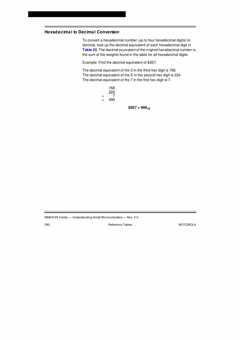
8/2/2019 122 Textbook
http://slidepdf.com/reader/full/122-textbook 290/331
Reference Tables
M68HC05 Family — Understanding Small Microcontrollers — Rev. 2.0
290 Reference Tables MOTOROLA
Hexadecimal to Decimal Conversion
To convert a hexadecimal number (up to four hexadecimal digits) to
decimal, look up the decimal equivalent of each hexadecimal digit inTable 20. The decimal equivalent of the original hexadecimal number is
the sum of the weights found in the table for all hexadecimal digits.
Example: Find the decimal equivalent of $3E7.
The decimal equivalent of the 3 in the third hex digit is 768.
The decimal equivalent of the E in the second hex digit is 224.
The decimal equivalent of the 7 in the first hex digit is 7.
768
224+ 7= 999
$3E7 = 99910

8/2/2019 122 Textbook
http://slidepdf.com/reader/full/122-textbook 291/331
Reference Tables
Hexadecimal to Decimal Conversion
M68HC05 Family — Understanding Small Microcontrollers — Rev. 2.0
MOTOROLA Reference Tables 291
Table 20. Hexadecimal to Decimal Conversion
15 Bit 8 7 Bit 0
15 12 11 8 7 4 3 0
4th Hex Digit 3rd Hex Digit 2nd Hex Digit 1st Hex Digit
Hex Decimal Hex Decimal Hex Decimal Hex Decimal
0 0 0 0 0 0 0 0
1 4,096 1 256 1 16 1 1
2 8,192 2 512 2 32 2 2
3 12,288 3 768 3 48 3 3
4 16,384 4 1,024 4 64 4 4
5 20,480 5 1,280 5 80 5 5
6 24,576 6 1,536 6 96 6 6
7 28,672 7 1,792 7 112 7 7
8 32,768 8 2,048 8 128 8 8
9 36,864 9 2,304 9 144 9 9
A 40,960 A 2,560 A 160 A 10
B 45,056 B 2,816 B 176 B 11
C 49,152 C 3,072 C 192 C 12
D 53,248 D 3,328 D 208 D 13
E 57,344 E 3,484 E 224 E 14
F 61,440 F 3,840 F 240 F 15

8/2/2019 122 Textbook
http://slidepdf.com/reader/full/122-textbook 292/331
Reference Tables
M68HC05 Family — Understanding Small Microcontrollers — Rev. 2.0
292 Reference Tables MOTOROLA
Decima l to Hexadecimal Conversion
To convert a decimal number (up to 65,53510) to hexadecimal, find the
largest decimal number in Table 20 that is less than or equal to thenumber you are converting. The corresponding hexadecimal digit is the
most significant hexadecimal digit of the result. Subtract the decimal
number found from the original decimal number to get the remaining
decimal value . Repeat the procedure using the remaining decimal value
for each subsequent hexadecimal digit.
Example: Find the hexadecimal equivalent of 77710.
The largest decimal number from Table 20, that is less than or equal to
77710
, is 76810
. This corresponds to a $3 in the third hexadecimal digit.
Subtract this 76810 from 77710 to get the remaining decimal value 910.
Next look in the column for the next lower order hexadecimal digit (2nd
hex digit in this case). Find the largest decimal value that is less than or
equal to the remaining decimal value . The largest decimal value in this
column that is less than or equal to 910 is 0, so you would place a 0 in
the second hex digit of your result.
910 minus 0 is the remaining decimal value 910.
Next look in the column for the next lower order hexadecimal digit (first
hex digit in this case). Find the largest decimal value that is less than or
equal to the remaining decimal value . The largest decimal value in this
column that is less than or equal to 910 is 9, so you would place a 9 in
the first hex digit of your result.
77710 = $309

8/2/2019 122 Textbook
http://slidepdf.com/reader/full/122-textbook 293/331
Reference Tables
Hexadecimal Values vs. M68HC05 Instructions
M68HC05 Family — Understanding Small Microcontrollers — Rev. 2.0
MOTOROLA Reference Tables 293
Hexadecimal Values vs. M68HC05 Instructions
Table 21 lists all hexadecimal values from $00 to $FF and the equivalent
M68HC05 instructions with their addressing modes. Since there are only210 M68HC05 instructions, 46 of the hexadecimal values do not
correspond to a legal instruction.
Table 21. Hexadecimal to M68HC05 Instruction Mnemonics (Sheet 1 of 5)
Operand InstructionAddressing
ModeOperand Instruction
AddressingMode
$00 BRSET0 Direct $20 BRA Relative
$01 BRCLR0 Direct $21 BRN Relative
$02 BRSET1 Direct $22 BHI Relative$03 BRCLR1 Direct $23 BLS Relative
$04 BRSET2 Direct $24 BCC Relative
$05 BRCLR2 Direct $25 BCS Relative
$06 BRSET3 Direct $26 BNE Relative
$07 BRCLR3 Direct $27 BEQ Relative
$08 BRSET4 Direct $28 BHCC Relative
$09 BRCLR4 Direct $29 BHCS Relative
$0A BRSET5 Direct $2A BPL Relative
$0B BRCLR5 Direct $2B BMI Relative
$0C BRSET6 Direct $2C BMC Relative
$0D BRCLR6 Direct $2D BMS Relative
$0E BRSET7 Direct $2E BIL Relative
$0F BRCLR7 Direct $2F BIH Relative
$10 BSET0 Direct $30 NEG Direct
$11 BCLR0 Direct $31 — —
$12 BSET1 Direct $32 — —
$13 BCLR1 Direct $33 COM Direct$14 BSET2 Direct $34 LSR Direct
$15 BCLR2 Direct $35 — —
$16 BSET3 Direct $36 ROR Direct
$17 BCLR3 Direct $37 ASR Direct

8/2/2019 122 Textbook
http://slidepdf.com/reader/full/122-textbook 294/331
Reference Tables
M68HC05 Family — Understanding Small Microcontrollers — Rev. 2.0
294 Reference Tables MOTOROLA
$18 BSET4 Direct $38 LSL Direct
$19 BCLR4 Direct $39 ROL Direct
$1A BSET5 Direct $3A DEC Direct
$1B BCLR5 Direct $3B — —
$1C BSET6 Direct $3C INC Direct
$1D BCLR6 Direct $3D TST Direct
$1E BSET7 Direct $3E — —
$1F BCLR7 Direct $3F CLR Direct
$40 NEGA Inherent $60 NEG Indexed 1
$41 — — $61 — —
$42 — — $62 — —
$43 COMA Inherent $63 COM Indexed 1
$44 LSRA Inherent $64 LSR Indexed 1
$45 — — $65 — —
$46 RORA Inherent $66 ROR Indexed 1
$47 ASRA Inherent $67 ASR Indexed 1
$48 LSLA Inherent $68 LSL Indexed 1
$49 ROLA Inherent $69 ROL Indexed 1
$4A DECA Inherent $6A DEC Indexed 1
$4B — — $6B — —
$4C INCA Inherent $6C INC Indexed 1
$4D TSTA Inherent $6D TST Indexed 1
$4E — — $6E — —
$4F CLRA Inherent $6F CLR Indexed 1
$50 NEGX Inherent $70 NEG Indexed 0
$51 — — $71 — —
$52 — — $72 — —
$53 COMX Inherent $73 COM Indexed 0
$54 LSRX Inherent $74 LSR Indexed 0
$55 — — $75 — —
$56 RORX Inherent $76 ROR Indexed 0
Table 21. Hexadecimal to M68HC05 Instruction Mnemonics (Sheet 2 of 5)
Operand InstructionAddressing
ModeOperand Instruction
AddressingMode

8/2/2019 122 Textbook
http://slidepdf.com/reader/full/122-textbook 295/331
Reference Tables
Hexadecimal Values vs. M68HC05 Instructions
M68HC05 Family — Understanding Small Microcontrollers — Rev. 2.0
MOTOROLA Reference Tables 295
$57 ASRX Inherent $77 ASR Indexed 0
$58 LSLX Inherent $78 LSL Indexed 0
$59 ROLX Inherent $79 ROL Indexed 0
$5A DECX Inherent $7A DEC Indexed 0
$5B — — $7B — —
$5C INCX Inherent $7C INC Indexed 0
$5D TSTX Inherent $7D TST Indexed 0
$5E — — $7E — —
$5F CLRX Inherent $7F CLR Indexed 0
$80 RTI Inherent $A0 SUB Immediate
$81 RTS Inherent $A1 CMP Immediate
$82 — — $A2 SBC Immediate
$83 SWI Inherent $A3 CPX Immediate
$84 — — $A4 AND Immediate
$85 — — $A5 BIT Immediate
$86 — — $A6 LDA Immediate
$87 — — $A7 — —
$88 — — $A8 EOR Immediate
$89 — — $A9 ADC Immediate
$8A — — $AA ORA Immediate
$8B — — $AB ADD Immediate
$8C — — $AC — —
$8D — — $AD BSR Relative
$8E STOP Inherent $AE LDX Immediate
$8F WAIT Inherent $AF — —
$90 — — $B0 SUB Direct
$91 — — $B1 CMP Direct
$92 — — $B2 SBC Direct
$93 — — $B3 CPX Direct
$94 — — $B4 AND Direct
$95 — — $B5 BIT Direct
Table 21. Hexadecimal to M68HC05 Instruction Mnemonics (Sheet 3 of 5)
Operand InstructionAddressing
ModeOperand Instruction
AddressingMode

8/2/2019 122 Textbook
http://slidepdf.com/reader/full/122-textbook 296/331
Reference Tables
M68HC05 Family — Understanding Small Microcontrollers — Rev. 2.0
296 Reference Tables MOTOROLA
$96 — — $B6 LDA Direct
$97 TAX Inherent $B7 STA Direct
$98 CLC Inherent $B8 EOR Direct
$99 SEC Inherent $B9 ADC Direct
$9A CLI Inherent $BA ORA Direct
$9B SEI Inherent $BB ADD Direct
$9C RSP Inherent $BC JMP Direct
$9D NOP Inherent $BD JSR Direct
$9E — — $BE LDX Direct
$9F TXA Inherent $BF STX Direct
$C0 SUB Extended $E0 SUB Indexed 1
$C1 CMP Extended $E1 CMP Indexed 1
$C2 SBC Extended $E2 SBC Indexed 1
$C3 CPX Extended $E3 CPX Indexed 1
$C4 AND Extended $E4 AND Indexed 1
$C5 BIT Extended $E5 BIT Indexed 1
$C6 LDA Extended $E6 LDA Indexed 1
$C7 STA Extended $E7 STA Indexed 1
$C8 EOR Extended $E8 EOR Indexed 1
$C9 ADC Extended $E9 ADC Indexed 1
$CA ORA Extended $EA ORA Indexed 1
$CB ADD Extended $EB ADD Indexed 1
$CC JMP Extended $EC JMP Indexed 1
$CD JSR Extended $ED JSR Indexed 1
$CE LDX Extended $EE LDX Indexed 1
$CF STX Extended $EF STX Indexed 1
$D0 SUB Indexed 2 $F0 SUB Indexed 0
$D1 CMP Indexed 2 $F1 CMP Indexed 0
$D2 SBC Indexed 2 $F2 SBC Indexed 0
$D3 CPX Indexed 2 $F3 CPX Indexed 0
$D4 AND Indexed 2 $F4 AND Indexed 0
Table 21. Hexadecimal to M68HC05 Instruction Mnemonics (Sheet 4 of 5)
Operand InstructionAddressing
ModeOperand Instruction
AddressingMode

8/2/2019 122 Textbook
http://slidepdf.com/reader/full/122-textbook 297/331
Reference Tables
Hexadecimal Values vs. M68HC05 Instructions
M68HC05 Family — Understanding Small Microcontrollers — Rev. 2.0
MOTOROLA Reference Tables 297
$D5 BIT Indexed 2 $F5 BIT Indexed 0
$D6 LDA Indexed 2 $F6 LDA Indexed 0
$D7 STA Indexed 2 $F7 STA Indexed 0
$D8 EOR Indexed 2 $F8 EOR Indexed 0
$D9 ADC Indexed 2 $F9 ADC indexed 0
$DA ORA Indexed 2 $FA ORA Indexed 0
$DB ADD Indexed 2 $FB ADD Indexed 0
$DC JMP Indexed 2 $FC JMP Indexed 0
$DD JSR Indexed 2 $FD JSR Indexed 0
$DE LDX Indexed 2 $FE LDX Indexed 0
$DF STX Indexed 2 $FF STX Indexed 0
Table 21. Hexadecimal to M68HC05 Instruction Mnemonics (Sheet 5 of 5)
Operand InstructionAddressing
ModeOperand Instruction
AddressingMode

8/2/2019 122 Textbook
http://slidepdf.com/reader/full/122-textbook 298/331
Reference Tables
M68HC05 Family — Understanding Small Microcontrollers — Rev. 2.0
298 Reference Tables MOTOROLA

8/2/2019 122 Textbook
http://slidepdf.com/reader/full/122-textbook 299/331
M68HC05 Family — Understanding Small Microcontrollers — Rev. 2.0
MOTOROLA Glossary 299
Glossary
1 K — One kilobyte or 102410 bytes. Similar to the use of the prefix in
kilogram, which means 1000 grams in the decimal numbering
system. 1024 is 210.
8-bit MCU — A microcontroller where data is communicated over a data
bus made up of eight separate data conductors. Members of the
M68HC05 Family of microcontrollers are 8-bit MCUs.
A — Abbreviation for accumulator in the M68HC05 MCU
accumulator — An 8-bit register in the CPU of the M68HC05. The
contents of this register may be used as an operand of an
arithmetic or logical instruction.
addressing mode — The way that the CPU obtains (addresses) the
information needed to complete an instruction. The M68HC05
CPU has six addressing modes:
• Inherent — The CPU needs no additional information from
memory to complete the instruction.
• Immediate — The information needed to complete the
instruction is located in the next memory location(s) after
the opcode.
• Direct — The low-order byte of the address of the operand
is located in the next memory location after the opcode, and
the high-order byte of the operand address is assumed to
be $00.
• Extended — The high-order byte of the address of the
operand is located in the next memory location after the
opcode, and the low-order byte of the operand address is
located in the next memory location after that.

8/2/2019 122 Textbook
http://slidepdf.com/reader/full/122-textbook 300/331
Glossary
M68HC05 Family — Understanding Small Microcontrollers — Rev. 2.0
300 Glossary MOTOROLA
• Indexed — The address of the operand depends upon the
current value in the X index register and a 0-, 8-, or 16-bit,
instruction-provided value.
• Relative — Used for branch instructions to specify the
destination address where processing will continue if the
branch condition is true.
address bus — The set of conductors that are used to select a specific
memory location so the CPU can write information into the
memory location or read its contents. If a computer has 11 wires
in its address bus, it can address 211 or 204810 memory
locations. In most M68HC05 MCUs, the address bus is not
accessible on external pins.
ALU — Arithmetic logic unit. This is the portion of the CPU of a computer
where mathematical and logical operations take place. Other
circuitry decodes each instruction and configures the ALU to
perform the necessary arithmetic or logical operations at each
step of an instruction.
ASCII — American Standard Code for Information Interchange. A widely
accepted correlation between alphabetic and numeric characters
and specific 7-bit binary numbers. Refer to Table 19.
Hexadecimal to ASCII Conversion.
analog — A signal that can have voltage level values that are neither the
VSS level nor the VDD level. For a computer to use such signals,
they must be converted into a binary number that corresponds to
the voltage level of the signal. An analog-to-digital converter can
be used to perform this conversion. By contrast, a digital signal
has only two possible values, 1 (≈VDD) or 0 (≈VSS).
application programs — Software programs that instruct a computer to
solve an application problem
arithmetic logic unit — This is the portion of the CPU of a computer
where mathematical and logical operations take place. Other
circuitry decodes each instruction and configures the ALU to
perform the necessary arithmetic or logical operations at each
step of an instruction.

8/2/2019 122 Textbook
http://slidepdf.com/reader/full/122-textbook 301/331
Glossary
M68HC05 Family — Understanding Small Microcontrollers — Rev. 2.0
MOTOROLA Glossary 301
assembler — A software program that translates source code
mnemonics into opcodes that can then be loaded into the
memory of a microcontroller.
assembly language — Instruction mnemonics and assemblerdirectives that are meaningful to programmers and can be
translated into an object code program that a microcontroller
understands. The CPU uses opcodes and binary numbers to
specify the operations that make up a computer program. These
numbers are not meaningful to people, so programmers use
assembly language mnemonics to represent instructions.
Assembler directives provide additional information such as the
starting memory location for a program. Labels are used to mean
an address or binary value.
base 2 — Binary numbers that use only the two digits, 0 and 1. Base 2
is the numbering system used by computers.
base 10 — Decimal numbers that use the 10 digits, 0 through 9. This is
the customary numbering system used by people.
base 16 — The hexadecimal numbering system. The 16 characters (0
through 9 and the letters A through F) are used to represent
hexadecimal values. One hexadecimal digit can exactly
represent a 4-bit binary value. Hexadecimal is used by people torepresent binary values because it is easier to use a 2-digit
number than the equivalent 8-digit binary number. Refer to
Table 1. Decimal, Binary, and Hexadecimal Equivalents.
BCD — Binary coded decimal is a notation that uses binary values to
represent decimal quantities. Each BCD digit uses four binary
bits. Six of the possible 16 binary combinations are considered
illegal.
binary — The numbering system used by computers because any
quantity can be represented by a series of 1s and 0s. Electrically,
these 1s and 0s are represented by voltage levels of
approximately VDD and VSS respectively.
bit — A single binary digit. A bit can hold a single value of 0 or 1.

8/2/2019 122 Textbook
http://slidepdf.com/reader/full/122-textbook 302/331
Glossary
M68HC05 Family — Understanding Small Microcontrollers — Rev. 2.0
302 Glossary MOTOROLA
black box — A hypothetical block of logic or circuitry that performs some
input to output transformation. A black box is used when the input
to output relationship is known but the means to achieve this
transformation is not known or is not important to the discussion.
branch instructions — Computer instructions that cause the CPU to
continue processing at a memory location other than the next
sequential address. Most branch instructions are conditional.
That is, the CPU will continue to the next sequential address (no
branch) if a condition is false or continue to some other address
(branch) if the condition is true.
breakpoint — During debugging of a program, it is useful to run
instructions until the CPU gets to a specific place in the program
and then enter a debugger program. A breakpoint is establishedat the desired address by temporarily substituting a software
interrupt (SWI) instruction for the instruction at that address. In
response to the SWI, control is passed to a debugging program.
byte — A set of exactly eight binary bits
C — Abbreviation for carry/borrow in the condition code register of the
M68HC05. When adding two unsigned 8-bit numbers, the C bit is
set if the result is greater than 255 ($FF).
CCR — Abbreviation for condition code register in the M68HC05. The
CCR has five bits (H, I, N, Z, and C) that can be used to control
conditional branch instructions. The values of the bits in the CCR
are determined by the results of previous operations. For
example, after a load accumulator (LDA) instruction, Z will be set
if the loaded value was $00.
central processor unit — The part of a computer that controls
execution of instructions
checksum — A value that results from adding a series of binarynumbers. When exchanging information between computers, a
checksum gives an indication about the integrity of the data
transfer. If values were transferred incorrectly, it is very unlikely
that the checksum would match the value that was expected.

8/2/2019 122 Textbook
http://slidepdf.com/reader/full/122-textbook 303/331
Glossary
M68HC05 Family — Understanding Small Microcontrollers — Rev. 2.0
MOTOROLA Glossary 303
clock — A square wave signal that is used to sequence events in a
computer
CMOS — Complimentary metal oxide semiconductor. A silicon
semiconductor processing technology that allows fabrication ofboth N-type and P-type transistors on the same integrated circuit.
Most modern microcontrollers use CMOS technology.
computer program — A series of instructions that cause a computer to
do something
computer system — A CPU plus other components needed to perform
a useful function. A minimum computer system includes a CPU,
a clock, memory, a program, and input/output interfaces.
condition code register — The CCR has five bits (H, I, N, Z, and C) that
canbe used to control conditional branch instructions. Thevalues
of the bits in the CCR are determined by the results of previous
operations. For example, after a load accumulator (LDA)
instruction, Z will be set if the loaded value was $00.
CPU — Central processor unit. The part of a computer that controls
execution of instructions
CPU cycles — A CPU clock cycle is one period of the internal bus-rate
clock. Normally, this clock is derived by dividing a crystaloscillator source by two or more so the high and low times will be
equal. The length of time required to execute an instruction is
measured in CPU clock cycles.
CPU registers — Memory locations that are wired directly into the CPU
logic instead of being part of the addressable memory map. The
CPU always has direct access to the information in these
registers. The CPU registers in an M68HC05 are:
• A — 8-bit accumulator
• X — 8-bit index register
• CCR — condition code register containing the H, I, N, Z,and C bits
• SP — stack pointer
• PC — program counter

8/2/2019 122 Textbook
http://slidepdf.com/reader/full/122-textbook 304/331
Glossary
M68HC05 Family — Understanding Small Microcontrollers — Rev. 2.0
304 Glossary MOTOROLA
CRT — Cathode ray tube. Also used as an informal expression to refer
to a complete communication terminal that has a keyboard and a
video display
cycles — See CPU cycles.
data bus — A set of conductors that are used to convey binary
information from a CPU to a memory location or from a memory
location to a CPU. In the M68HC05, the data bus is eight bits.
decimal — Base 10 numbers use the digits 0 through 9. This is the
numbering system normally used by humans.
development tools — Software or hardware devices that are used to
develop computer programs and application hardware. Examples
of software development tools include text editors, assemblers,
debug monitors, and simulators. Examples of hardware
development tools include emulators, logic analyzers, and PROM
programmers. An in-circuit simulator combines a software
simulator with hardware interfaces.
digital — A binary logic system where signals can have only two states,
0 (≈VSS) or 1 (≈VDD).
direct address — Any address within the first 256 addresses of memory
($0000 through $00FF). The high-order byte of these addressesis always $00. Special instructions allow these addresses to be
accessed using only the low-order byte of their address. These
instructions automatically fill in the assumed $00 value for the
high-order byte of the address.
direct addressing mode — Direct addressing mode uses a
program-supplied value for the low-order byte of the address of
an operand. The high-order byte of the operand’s address is
assumed to be $00, so it does not have to be explicitly specified.
direct page — The first 256 bytes of memory, $0000 through $00FF
EEPROM — Electrically erasable, programmable read-only memory. A
non-volatile type of memory that can be erased and
reprogrammed by program instructions. Since no special power

8/2/2019 122 Textbook
http://slidepdf.com/reader/full/122-textbook 305/331
Glossary
M68HC05 Family — Understanding Small Microcontrollers — Rev. 2.0
MOTOROLA Glossary 305
supplies or ultra-violet light source is needed, the contents of this
kind of memory can be changed without removing the MCU from
the application system.
effective address — The address where an instruction operand islocated. The addressing mode of an instruction determines how
the CPU calculates the effective address of the operand.
embedded — When an appliance contains a microcontroller, the MCU
is said to be an embedded controller. Often, the end user of the
appliance is not aware (or does not care) that there is a computer
inside.
EPROM — Erasable, programmable read-only memory. A non-volatile
type of memory that can be erased by exposure to an ultra-violetlight source. MCUs that have EPROM are easily recognized
because the package has a quartz window to allow exposure to
the ultra-violet light. If an EPROM MCU is packaged in an opaque
plastic package, it is called a one-time-programmable (OTP)
MCU because there is no way to expose the EPROM to
ultra-violet light.
extended addressing mode — In this addressing mode, the high-order
byte of the address of the operand is located in the next memory
location after the opcode. The low-order byte of the operand’saddress is located in the second memory location after the
opcode.
fetching a vector — When the CPU is reset or responds to an interrupt,
the contents of a specific pair of memory locations is loaded into
the program counter and processing continues from the loaded
address. The process of reading these two locations is called
fetching the vector.
flowchart — A symbolic means to show the sequence of steps required
to perform an operation. A flowchart not only tells what needs to
be done, but also the order that the steps should be done in.

8/2/2019 122 Textbook
http://slidepdf.com/reader/full/122-textbook 306/331
Glossary
M68HC05 Family — Understanding Small Microcontrollers — Rev. 2.0
306 Glossary MOTOROLA
H — Abbreviation for half-carry in the condition code register of the
M68HC05. This bit indicates a carry from the low-order four bits
of an 8-bit value to the high-order four bits. This status indicator
is used during BCD calculations.
half flip flop — A half flip flop (HFF) has a transparent condition and a
latched condition. In the transparent condition (clock input equal
logic 1), the Q output is always equal to the logic level presented
at the input. In the latched condition (clock input equals logic 0),
the output maintins the logic level that was present when the flip
flop was last in the transparent condition.
hexadecimal — The base 16 numbering system. The 16 characters (0
through 9 and the letters A through F) are used to represent
hexadecimal values. One hexadecimal digit can exactlyrepresent a 4-bit binary value. Hexadecimal is used by people to
represent binary values because it is easier to use a 2-digit
number than the equivalent 8-digit binary number. Refer to
Table 1. Decimal, Binary, and Hexadecimal Equivalents.
high order — The leftmost digit(s) of a number. Five is the high-order
digit of the number 57.
I — Abbreviation for interrupt mask bit in the condition code register of
the M68HC05
I/O — Input/output interfaces between a computer system and the
external world. A CPU reads an input to sense the level of an
external signal and writes to an output to change the level on an
external signal.
immediate addressing mode — In immediate addressing mode, the
operand is located in the next memory location(s) after the
opcode.
inherent addressing mode — In inherent addressing mode, the CPUalready inherently knows everything it needs to know to complete
the instruction. The operands (if there are any) are in the CPU
registers.
in-circuit simulator — A simulator with hardware interfaces that allows

8/2/2019 122 Textbook
http://slidepdf.com/reader/full/122-textbook 307/331
Glossary
M68HC05 Family — Understanding Small Microcontrollers — Rev. 2.0
MOTOROLA Glossary 307
connection into an application circuit. The in-circuit simulator
replaces the MCU and behaves as a real MCU would. The
developer has greater control and visibility of internal MCU
operations because they are being simulated by instructions in
the host computer. An in-circuit simulator, like other simulators, is
not as fast as a real MCU.
indexed addressing mode — In indexed addressing mode, the current
value of the index register is added to a 0-, 8-, or 16-bit value in
the instruction to get the effective address of the operand. There
are separate opcodes for 0-, 8-, and 16-bit variations of indexed
mode instructions, so the CPU knows how many additional
memory locations to read after the opcode.
index register (X) — An 8-bit CPU register in the M68HC05 that is usedin indexed addressing mode. X, its abbreviation,canalso be used
as a general-
purpose 8-bit register (in addition to the 8-bit accumulator).
input/output — Interfaces between a computer system and the external
world. A CPU reads an input to sense the level of an external
signal and writes to an output to change the level on an external
signal.
instruction decoder — The portion of a CPU that receives an
instruction opcode and produces the necessary control signals sothat the rest of the CPU will perform the desired operations.
instructions — Instructions are operations that a CPU can perform.
Instructions are expressed by programmers as assembly
language mnemonics. A CPU interprets an opcode and its
associated operand(s) as an instruction.
instruction set — The instruction set of a CPU is the set of all
operations that the CPU knows how to perform. One way to
represent an instruction set is with a set of shorthand mnemonics,such as LDA meaning load A. Another representation of an
instruction set is the set of opcodes that are recognized by the
CPU.

8/2/2019 122 Textbook
http://slidepdf.com/reader/full/122-textbook 308/331
Glossary
M68HC05 Family — Understanding Small Microcontrollers — Rev. 2.0
308 Glossary MOTOROLA
inverter — A simple logic circuit that produces an output logic level that
is the opposite of the level presented to its input.
kilobyte — One kilobyte is 102410 bytes. Similar to the use of the prefix
in kilogram, which means 1000 grams in the decimal numberingsystem. 1024 is 210.
label — A name that is assigned (by a programmer) to a specific
address or binary value. When a program containing a lable is
assembled, the label is replaced by the binary value it represents.
Programs typically include many labels.
latch — A logic circuit that maintains a stable output state even after the
input has been removed or changed. A clock control input
determines when the latch will capture the input state and applyit to the output.
least significant bit — LSB, the rightmost digit of a binary value
listing — A program listing shows the binary numbers that the CPU
needs alongside the assembly language statements that the
programmer wrote. The listing is generated by an assembler in
the process of translating assembly language source statements
into the binary information that the CPU needs.
logic 1 — A voltage level approximately equal to the VDD power supply
logic 0 — A voltage level approximately equal to VSS (ground)
low order — The rightmost digit(s) of a number. Seven is the low-order
digit of the number 57.
LSB — Least significant bit. The rightmost digit of a binary value
machine codes — The binary codes that are processed by the CPU as
instructions. Machine code includes both opcodes and operand
data.
mainframe computer — A large computer system that is usually
confined to a special room. Mainframe computers are used for
large information processing jobs likemaintaining a database of
all policyholders for an insurance company.

8/2/2019 122 Textbook
http://slidepdf.com/reader/full/122-textbook 309/331
Glossary
M68HC05 Family — Understanding Small Microcontrollers — Rev. 2.0
MOTOROLA Glossary 309
mass storage — A very large capacity storage device such as a
magnetic disk. Information in a mass storage device takes longer
to access than information in the memory map of a CPU.
MCU — Microcontroller unit. A complete computer system, including aCPU, memory, a clock oscillator, and I/O on a single integrated
circuit.
memory location — In the M68HC05, each memory location holds one
byte of data and has a unique address. To store information into
a memory location, the CPU places the address of the location on
the address bus, the data information on the data bus, and
asserts the write signal. To read information from a memory
location, the CPU places the address of the location on the
address bus and asserts the read signal. In response to the readsignal, the selected memory location places its data onto the data
bus.
memory map — A pictorial representation of all memory locations in a
computer system. A memory map is similar to a city street map in
that it shows where things are located.
memory-mapped I/O — In this type of system, I/O and control registers
are accessed in the same way as RAM or ROM memory
locations. Any instruction that can be used to access memory canalso be used to access I/O registers.
microcontroller — A complete computer system, including a CPU,
memory, a clock oscillator, and I/O on a single integrated circuit.
microprocessor — A microprocessor is similar to a microcontroller
except that one or more of the subsystems needed to make a
complete computer system is not included on the same chip with
the CPU. A microprocessor typically includes a CPU and a clock
oscillator but does not include program memory or I/O registers.
mnemonic — Three to five letters that represent a computer operation.
For example, the mnemonic form of the load accumulator
instruction is LDA.

8/2/2019 122 Textbook
http://slidepdf.com/reader/full/122-textbook 310/331
Glossary
M68HC05 Family — Understanding Small Microcontrollers — Rev. 2.0
310 Glossary MOTOROLA
monitor program — A software program that is intended to assist in
system development. A typical monitor program allows a user to
examine and change memory or CPU register contents, set
breakpoints, and selectively execute application programs.
most significant bit — The leftmost digit of a binary value
MSB — Most significant bit. The leftmost digit of a binary value
N — Abbreviation for negative, a bit in the condition code register of the
M68HC05. In twos-complement computer notation, positive
signed numbers have a 0 in their MSB and negative numbers
have a 1 in their MSB. The N condition code bit reflects the sign
of the result of an operation. After a load accumulator instruction,
the N bit will be set if the MSB of the loaded value was a 1.
NAND gate — A basic logic circuit. The output of a NAND gate is a logic
0 when all of its inputs are logic 1s. The output of a NAND gate is
a logic 1 if any of its inputs are logic 0.
non-volatile — A type of memory that does not forget its contents when
power is turned off. ROM, EPROM, and EEPROM are all
non-volatile memories.
NOR gate — A basic logic circuit. The output of a NOR gate is a logic 0
when any of its inputs are logic 1s. The output of a NOR gate is alogic 1 if all of its inputs are logic 0.
object code file — A text file containing numbers that represent the
binary opcodes and data of a computer program. An object code
file can be used to load binary information into a computer
system. Motorola uses the S-record file format for object code
files. See Figure 35. S-Record File for Example Program.
octal — Base 8 numbers that use the characters 0 through 7 to
represent sets of three binary bits. Octal is seldom used inmodern computer work.
one — A logic high level (≈VDD)

8/2/2019 122 Textbook
http://slidepdf.com/reader/full/122-textbook 311/331
Glossary
M68HC05 Family — Understanding Small Microcontrollers — Rev. 2.0
MOTOROLA Glossary 311
ones complement — To get the logical ones-complement of a binary
value, invert each bit.
opcode — A binary code that instructs the CPU to do a specific
operation in a specific way. The M68HC05 CPU recognizes 210unique 8-bit opcodes that represent addressing mode variations
of 62 basic instructions.
operand — An input value to a logical or mathematical operation
oscillator — A circuit that produces a constant frequency square wave
that is used by the computer as a timing and sequencing
reference. A microcontroller typically includes all elements of this
circuit except the frequency-determining component(s), the
crystal or R-C (resistor-capacitor)components.
OTP — See OTPROM.
OTPROM — A non-volatile type of memory that can be programmed but
cannot be erased. An OTPROM is an EPROM MCU that is
packaged in an opaque plastic package. It is called a
one-time-programmable MCU because there is no way to expose
the EPROM to ultra-violet light.
parity — An extra bit in a binary word that is intended to indicate the
validity of the remaining bits in the word. In even parity, the paritybit is set or cleared as needed to make the total number of logic
1s in the word (including the parity bit) equal to an even number
(0, 2, 4, etc.).
PC — Abbreviation for program counter, a CPU register in the M68HC05
MCU. Also used as an abbreviation for personal computer.
personal computer — A small computer system that is normally used
by a single person to process information
playing computer — A learning technique in which you pretend to be a
CPU that is executing the instructions of a program
pointer register — An index register is sometimes called a pointer
register because its contents are used in the calculation of the
address of an operand. A straightforward example is an

8/2/2019 122 Textbook
http://slidepdf.com/reader/full/122-textbook 312/331
Glossary
M68HC05 Family — Understanding Small Microcontrollers — Rev. 2.0
312 Glossary MOTOROLA
indexed-no offset instruction where the X register contains the
direct address of (points to) the operand.
program — A set of computer instructions that cause a computer to
perform an application task
program counter — The program counter (PC) is the CPU register that
holds the address of the next instruction or operand that the CPU
will use.
programming model — The registers of a particular CPU. The
programming model of the M68HC05 CPU is shown in Figure 23.
Programming Model.
PROM — Programmable read-only memory. A non-volatile type of
memory that can be programmed after it is manufactured.
EPROM and EEPROM are two types of PROM memory.
pulled — The act of reading a value from the stack. In the M68HC05, a
value is pulled by this sequence of operations: First, the stack
pointer register is incremented so that it points at the last value
that was saved on the stack. Next the value that is at the address
contained in the stack pointer register is read into the CPU.
pushed — The act of storing a value at the address contained in the
stack pointer register and then decrementing the stack pointer soit points at the next available stack location
RAM — Random access memory. Any RAM location can be read or
written by the CPU. The contents of a RAM memory location
remain valid until the CPU writes a different value or until power
is turned off.
read — Transfer the contents of a memory location to the CPU
record — One line of an object code text file. See S-record.

8/2/2019 122 Textbook
http://slidepdf.com/reader/full/122-textbook 313/331
Glossary
M68HC05 Family — Understanding Small Microcontrollers — Rev. 2.0
MOTOROLA Glossary 313
registers — Memory locations that are wired directly into the CPU logic
instead of being part of the addressable memory map. The CPU
always has direct access to the information in these registers.
The CPU registers in an M68HC05 are:
• A — 8-bit accumulator
• X — 8-bit index register
• CCR — condition code register containing the H, I, N, Z,
and C bits
• SP — stack pointer
• PC — program counter
Memory locations that hold status and control information for
on-chip peripherals are called I/O and control registers.
relative addressing mode — Relative addressing mode is used to
calculate the destination address for branch instructions. If the
branch condition is true, the signed 8-bit value after the opcode is
added to the current value of the program counter to get the
address where the CPU will fetch the next instruction.
relative offset — An 8-bit, signed twos-complement value that is added
to the program counter when a branch condition is true. The
relative offset is located in the byte after a branch opcode.
reset — Reset is used to force a computer system to a known starting
point and to force on-chip peripherals to known starting
conditions.
reset vector — The contents of the last two memory locations in an
M68HC05 MCU are called the reset vector. As the MCU leaves
reset, the program counter is loaded with the contents of these
two locations so the first instruction after reset will be fetched from
that address.
ROM — Read-only memory. A type of memory that can be read but
cannot be changed (written). The contents of ROM must be
specified before manufacturing the MCU.

8/2/2019 122 Textbook
http://slidepdf.com/reader/full/122-textbook 314/331
Glossary
M68HC05 Family — Understanding Small Microcontrollers — Rev. 2.0
314 Glossary MOTOROLA
S-record — A Motorola standard format used for object code files. See
Figure 35. S-Record File for Example Program.
simulator — A computer program that copies the behavior of a real
MCU
source code — See source program
source program — A text file containing instruction mnemonics, labels,
comments, and assembler directives. The source file is
processed by an assembler to produce a composite listing and an
object file representation of the program.
SP — Abbreviation for stack pointer, a CPU register in the M68HC05
MCU
stack — A mechanism for temporarily saving CPU register values
during interrupts and subroutines. The CPU maintains this
structure with the stack pointer register which contains the
address of the next available storage location on the stack. When
a subroutine is called, the CPU pushes (stores) the low-order and
high-order bytes of the return address on the stack before starting
the subroutine instructions. When the subroutine is done, a
return-from-subroutine (RTS) instruction causes the CPU to
recover the return address from the stack and continue
processing where it left off before the subroutine. Interrupts work
in the same way except all CPU registers are saved on the stack
instead of just the program counter.
stack pointer — A CPU register that holds the address of the next
available storage location on the stack
subroutine — A sequence of instructions that need to be used more
than once in the course of a program. The last instruction in a
subroutine is a return-from-subroutine (RTS) instruction. At each
place in the main program where the subroutine instructions areneeded, a jump- or branch-to-subroutine (JSR or BSR)
instruction is used to call the subroutine. The CPU leaves the flow
of the main program to execute the instructions in the subroutine.
When the RTS instruction is executed, the CPU returns to the
main program where it left off.
8/2/2019 122 Textbook
http://slidepdf.com/reader/full/122-textbook 315/331
Glossary
M68HC05 Family — Understanding Small Microcontrollers — Rev. 2.0
MOTOROLA Glossary 315
three-state buffer — The output of a three-state buffer can be a logic 0,
a logic 1, or a high impedance (as if connected to nothing). An
enable input controls the high impedance (off) state vs. the low
impedance (on) state. When the buffer is on, the output has the
same logic level as the input (1 or 0). When the buffer is off, the
output acts like an open circuit.
transducer — A device that converts some physical property, such as
pressure, into electrical signals that can be used by a computer
transmission gate — A basic logic circuit used in microcontrollers. A
transmission gate works like a series switch that is controlled by
a logic level signal. When the control input is a logic 0, the
transmission gate acts like an open circuit. When the control input
is a logic 1, the transmission gate acts like a short circuit.
twos complement — A means of performing binary subtraction using
addition techniques. The most significant bit of a twos
complement number indicates the sign of the number (1 indicates
negative). The twos complement negative of a number is
obtained by inverting each bit in the number and then adding 1 to
the result. For example, the twos complement negative of
0000 0011 (310) is 1111 1100 + 0000 0001 = 1111 1101.
variable — A value that changes during the course of executing aprogram
V DD — The positive power supply to a microcontroller, typically 5 volts dc
vector — A pointer (address) that indicates where the CPU should
continue processing instructions after an interrupt or reset
V SS — The 0 volt dc power supply return for a microcontroller
volatile — A type of memory that forgets its contents when power is
turned off. RAM is a type of volatile memory. In modernmicrocontrollers, it takes very little power to maintain the contents
of a RAM under good conditions. In some cases, the contents of
RAM and registers may appear to be unchanged after a short
interruption of power.

8/2/2019 122 Textbook
http://slidepdf.com/reader/full/122-textbook 316/331
Glossary
M68HC05 Family — Understanding Small Microcontrollers — Rev. 2.0
316 Glossary MOTOROLA
word — A group of binary bits. Some larger computers consider a set of
16 bits to be a word, but this is not a universal standard.
write — The transfer of a byte of data from the CPU to a memory
location
X — Abbreviation for index register, a CPU register in the M68HC05
MCU
Z — Abbreviation for zero, a bit in the condition code register of the
M68HC05. A compare instruction subtracts the contents of the
tested value from a register. If the values were equal, the result of
this subtraction would be zero, so the Z bit would be set. After a
load accumulator instruction, the Z bit will be set if the loaded
value was $00.
zero — A logic low level (VSS)
zero crossings — When an alternating current signal goes from a
positive to a negative or from a negative to a positive value, it is
called a zero crossing. The 60-Hz ac power line crosses zero
every 8.33 milliseconds.

8/2/2019 122 Textbook
http://slidepdf.com/reader/full/122-textbook 317/331
M68HC05 Family — Understanding Small Microcontrollers — Rev. 2.0
MOTOROLA Index 317
Index
AAccumulator (A). . . . . . . . . . . . . . . . . . . 68, 74, 75, 100, 102, 133, 299
Address bus. . . . . . . . . . . . . . . . . . . 53, 54, 56, 63, 66, 68, 74, 75, 300
Addressing mode. . . . . . . . . . . . . . . . . . . . 98, 104, 133, 146, 150, 299
direct . . . . . . . . . . . . . . . . . . . . . . . . . . . . . . . . . . . . . . . . . . . . . 110
extended . . . . . . . . . . . . . . . . . . . . . . . . . . . . . . . . . . . . . . . . . . 108
immediate. . . . . . . . . . . . . . . . . . . . . . . . . . . . . . . . . . . . . . . 75, 107
indexed. . . . . . . . . . . . . . . . . . . . . . . . . . . . . . . . . . . . . . . . . . . . 112inherent . . . . . . . . . . . . . . . . . . . . . . . . . . . . . . . . . . . . . . . . . . . 105
relative . . . . . . . . . . . . . . . . . . . . . . . . . . . . . . . . . . . . . . . . . . . . 118
Analog . . . . . . . . . . . . . . . . . . . . . . . . . . . . . . . . . . . . . . . . . . . . 19, 300
Analog switch . . . . . . . . . . . . . . . . . . . . . . . . . . . . . . . . . . . . . . . . . . 45
Analog-to-digital converter (A-to-D). . . . . . . . . . . . . . . . . 183, 187, 215
Architecture
computer . . . . . . . . . . . . . . . . . . . . . . . . . . . . . . . . . . . . . . . . . . . 66
Von Neumann . . . . . . . . . . . . . . . . . . . . . . . . . . . . . . . . . . . . . . . 66
Arithmetic logic unit (ALU) . . . . . . . . . . . . . . . . . . . . . . . . . . 78, 98, 300
ASCII . . . . . . . . . . . . . . . . . . . . . . . . . . . . . . . 33, 36, 67, 105, 288, 300
code . . . . . . . . . . . . . . . . . . . . . . . . . . . . . . . . . . . . . . . . . . . . . . .30
conversion to/from hexadecimal . . . . . . . . . . . . . . . . . 31, 288, 289
Assembler . . . . . . . . . . . . . . . . . . 32, 36, 105, 143, 146, 147, 156, 301
directive . . . . . . . . . . . . . . . . . . . . . . . . . . . . . . . . . . . 145, 149, 156
listing . . . . . . . . . . . . . . . . . . . . . . . . . . . . . 143, 144, 145, 156, 308
Assembly language . . . . . . . . . . . . . . . . . . . . . . . . . . . . . . . . . 139, 301
B
Base 10 . . . . . . . . . . . . . . . . . . . . . . . . . . . . . . . . . . . . . . . . 27, 28, 301Base 16 . . . . . . . . . . . . . . . . . . . . . . . . . . . . . . . . . . . . . . . . . . . 28, 301
Base 2 . . . . . . . . . . . . . . . . . . . . . . . . . . . . . . . . . . . . . . . . . 27, 28, 301
Base 8 . . . . . . . . . . . . . . . . . . . . . . . . . . . . . . . . . . . . . . . . . . . . . . . . .32

8/2/2019 122 Textbook
http://slidepdf.com/reader/full/122-textbook 318/331
Index
M68HC05 Family — Understanding Small Microcontrollers — Rev. 2.0
318 Index MOTOROLA
Binary . . . . . . . . . . . . . . . . . . . . . . . . 28, 30, 32, 36, 98, 105, 150, 301
conversion to/from decimal, hexadecimal . . . . . . . . . . . . . . . . . . 29
conversion to/from octal, hexadecimal . . . . . . . . . . . . . . . . . . . . .33
Binary coded decimal
conversion to/from decimal, binary . . . . . . . . . . . . . . . . . . . . . . . 35
Binary coded decimal (BCD) . . . . . . . . . . . . . . . . 27, 34, 101, 102, 301
Bit . . . . . . . . . . . . . . . . 22, 52, 54, 60, 62, 76, 150, 160, 161, 183, 301
carry/borrow (C) . . . . . . . . . . . . . . . . . . . . . . . . . . . . . . . . . . . . . 102
half-carry (H) . . . . . . . . . . . . . . . . . . . . . . . . . . . . . . . . . . . . . . . 101
interrupt mask (I) . . . . . . . . . . . . . . . . . . . . . . . . . . . . . . . . . . . . 101
negative (N) . . . . . . . . . . . . . . . . . . . . . . . . . . . . . . . . . . . . . . . . 101
zero (Z). . . . . . . . . . . . . . . . . . . . . . . . . . . . . . . . . . . . . . . . . . . . 102
Black box. . . . . . . . . . . . . . . . . . . . . . . . . . . . . . . . . . . . . . . . . . 74, 302
Branch . . . . . . . . . . . . . . . . . . . . . . . . . . . . . . . . . . . . . . . . . . 76, 79, 84instructions. . . . . . . . . . . . . . . . . . . . . . . . . . 69, 119, 120, 123, 302
Branch-to-subroutine (BSR) . . . . . . . . . . . . . . . . . . . . 76, 85, 141, 250
Breakpoint . . . . . . . . . . . . . . . . . . . . . . . . . . . . . . . . . . . . . . . .155, 302
Buffer . . . . . . . . . . . . . . . . . . . . . . . . . . . . . . . . . . . . . . . . . . . . . . . . . 44
three-state . . . . . . . . . . . . . . . . . . . . . . . . . . . . . . . . . . . . . . . 46, 49
Bus
address . . . . . . . . . . . . . . . . . . . . . . . . . . . . . . . . . . . . . . .66, 68, 74
data . . . . . . . . . . . . . . . . . . . . . . . . . . . . . . . . . . . . . . . . . . . . 66, 75
Byte . . . . . . . . . . . . . . . . . . . . . . . . . . . . . . . . . . . . 22, 54, 67, 148, 302
gigabyte . . . . . . . . . . . . . . . . . . . . . . . . . . . . . . . . . . . . . . . . . . . . 54kilobyte . . . . . . . . . . . . . . . . . . . . . . . . . . . . . . . . . . . . . . . . . . . . . 54
megabyte . . . . . . . . . . . . . . . . . . . . . . . . . . . . . . . . . . . . . . . . . . .54
CC (bit in condition code register) . . . . . . . . . . . . . . . . 68, 102, 195, 302
Central processor unit (CPU) . . . . . . . . . . . . . . . . .18, 20, 25, 302, 303
Checksum . . . . . . . . . . . . . . . . . . . . . . . . . . . . . . . . . . . . . . . . 148, 302
Clock . . . . . . . . . . . . . . . . . . .21, 25, 69, 74, 77, 94, 105, 181, 184, 303
CMOS . . . . . . . . . . . . . . . . . . . . . . . . . . . . . . . . . . . . . . . . . 38, 39, 303N-type transistors. . . . . . . . . . . . . . . . . . . . . . . . . . . . . . . . . . . . . 39
P-type transistors . . . . . . . . . . . . . . . . . . . . . . . . . . . . . . . . . . . . . 39

8/2/2019 122 Textbook
http://slidepdf.com/reader/full/122-textbook 319/331
Index
M68HC05 Family — Understanding Small Microcontrollers — Rev. 2.0
MOTOROLA Index 319
Computer
architecture . . . . . . . . . . . . . . . . . . . . . . . . . . . . . . . . . . . . . . . . . 66
kinds. . . . . . . . . . . . . . . . . . . . . . . . . . . . . . . . . . . . . . . . . . . . . . . 25
memory . . . . . . . . . . . . . . . . . . . . . . . . . . . . . . . . . . . . . . . . . . . . 52
parts . . . . . . . . . . . . . . . . . . . . . . . . . . . . . . . . . . . . . . . . . . . . . . .25
playing . . . . . . . . . . . . . . . . . . . . . . . . . . . . . . . . . . . . . . . . . . 80, 94
program . . . . . . . . . . . . . . . . . . . . . . . . . . . . . . . . . . . . . 20, 23, 303
system . . . . . . . . . . . . . . . . . . . . . . . . . . . . . . . . . . . . . . . . . 18, 303
Computer program . . . . . . . . . . . . . . . . . . . . . . . . . . . . . . . 20, 23, 303
Computer system . . . . . . . . . . . . . . . . . . . . . . . . . . . . . . . . . . . 18, 303
Condition code register (CCR) . . . . . . . . . . . . . . . . 68, 69, 75, 86, 100,
101, 133, 302, 303
Conditional branch. . . . . . . . . . . . . . . . . . . . . . . . . . . . . . . . 76, 84, 142
COPwatchdog timer . . . . . . . . . . . . . . . . . . . . . . . . . . . . . . . . . . . .87, 95
CPU. . . . . . . . . . . . . . . . . . . . . . . . . . . . . . . . . . . . . . . . . . . . . . . 80, 98
control circuitry. . . . . . . . . . . . . . . . . . . . . . . . . . . . . . . . . . . . . . . 99
instruction set . . . . . . . . . . . . . . . . . . . . . . . . . . . . . . . . . . . . . . .126
instructions. . . . . . . . . . . . . . . . . . . . . . . . . . . . . . . . . . . . . . . . . . 73
operation . . . . . . . . . . . . . . . . . . . . . . . . . . . . . . . . . . . . . . . . . . . 73
register . . . . . . . . . . . . . . . . . . . . . . . . . . . . . . . . . . . . . . . . . . 67, 99
view of a program. . . . . . . . . . . . . . . . . . . . . . . . . . . . . . . . . . . . . 70
CRT . . . . . . . . . . . . . . . . . . . . . . . . . . . . . . . . . . . . . . . . . . . . . . 20, 304
Cycles . . . . . . . 21, 69, 74, 75, 77, 87, 92, 94, 105, 110, 142, 153, 303
DData bus . . . . . . . . . . . . . . . . . . . . . . . . . . . . . . . . . . . . 56, 66, 75, 304
Data multiplexer. . . . . . . . . . . . . . . . . . . . . . . . . . . . . . . . . . . . . . . . . 45
Decimal . . . . . . . . . . . . . . . . . . . . . . . . . . . . . . . . 28, 34, 105, 152, 304
conversion to/from hexadecimal . . . . . . . . . . . . . 29, 290, 291, 292
conversion to/from hexadecimal, binary. . . . . . . . . . . . . . . . . 29, 35
Development tools. . . . . . . . . . . . . . . . . . . . . . . . . . . . . . . . . . 154, 304
Dexterity . . . . . . . . . . . . . . . . . . . . . . . . . . . . . . . . . . . . . . . . . . . . . 153Digital. . . . . . . . . . . . . . . . . . . . . . . . . . . . . . . . . . . . . . . . . . 19, 27, 304
Digital-to-analog converter (D-to-A). . . . . . . . . . . . . . . . . 183, 187, 215
Direct address . . . . . . . . . . . . . . . . . . . . . . . . . . . . . . . . 74, 76, 79, 304
Direct addressing mode. . . . . . . . . . . . . 60, 64, 74, 104, 110, 111, 120,
134, 146, 150, 304

8/2/2019 122 Textbook
http://slidepdf.com/reader/full/122-textbook 320/331
Index
M68HC05 Family — Understanding Small Microcontrollers — Rev. 2.0
320 Index MOTOROLA
Direct page . . . . . . . . . . . . . . . . . . . . . . . . . . . . . . . . . . . . . . . 110, 304
Duty cycle . . . . . . . . . . . . . . . . . . . . . . . . . . . . . . . . . . . . . . . . 187, 201
EEEPROM . . . . . . . . . . . . . . . . . . . . . . . . . . . .22, 56, 63, 183, 216, 304
Effective address. . . . . . . . . . . . . . . . . . . . . . . . . . . . . . . 100, 104, 305
Embedded . . . . . . . . . . . . . . . . . . . . . . . . . . . . . . . . . . . . . . . . . 25, 305
EPROM . . . . . . . . . . . . . . . . . . . . . . . . . . . . . . 22, 55, 63, 70, 155, 305
Equate directive (EQU) . . . . . . . . . . . . . . . . . . . . . . . . . . 145, 149, 160
Extended address . . . . . . . . . . . . . . . . . . . . . . . . . . . . . . . . . . . . . . . 78
Extended addressing mode . . . . . . . . . . .104, 108, 109, 133, 150, 305
FFCB directive . . . . . . . . . . . . . . . . . . . . . . . . . . . . . . . . . . . . . . . . . . 150
FDB directive . . . . . . . . . . . . . . . . . . . . . . . . . . . . . . . . . .150, 162, 178
Fetching a vector. . . . . . . . . . . . . . . . . . . . . . . . . . . . . . . . . . . . . . . 305
Fetching the reset vector. . . . . . . . . . . . . . . . . . . . . . . . . . . . . . . . . . 86
Flip flop . . . . . . . . . . . . . . . . . . . . . . . . . . . . . . . . . . . . . . . . . . . . . . . .44
Flowchart . . . . . . . . . . . . . . . . . . . . . .76, 136, 137, 138, 147, 156, 305
GGate. . . . . . . . . . . . . . . . . . . . . . . . . . . . . . . . . . . . . . . . . . . . . . . 37, 40
buffer . . . . . . . . . . . . . . . . . . . . . . . . . . . . . . . . . . . . . . . . . . . . . . 47
inverter . . . . . . . . . . . . . . . . . . . . . . . . . . . . . . . . . . . . . . . . . . . . . 40
NAND. . . . . . . . . . . . . . . . . . . . . . . . . . . . . . . . . . . . . . . . . . . 40, 41
NOR . . . . . . . . . . . . . . . . . . . . . . . . . . . . . . . . . . . . . . . . . . . . 40, 42
transmission. . . . . . . . . . . . . . . . . . . . . . . . . . . . . . . . . . . . . . 44, 49
Gigabyte . . . . . . . . . . . . . . . . . . . . . . . . . . . . . . . . . . . . . . . . . . . . . . 54
HH (bit in condition code register) . . . . . . . . . . . . . . . . 68, 101, 102, 306
Half flip flop (HFF) . . . . . . . . . . . . . . . . . . . . . . . . . . . . .48, 49, 57, 306
Hexadecimal . . . . . . . . . . . . . . . . . . . . . . . . . . 28, 29, 36, 105, 148, 152, 306
conversion to /from decimal . . . . . . . . . . . . . . . . . . . . . . . . . . . . 290
conversion to/from ASCII . . . . . . . . . . . . . . . . . . . . . . .31, 288, 289
conversion to/from decimal . . . . . . . . . . . . . . . . . . . . . . . . .291, 292
conversion to/from decimal, binary . . . . . . . . . . . . . . . . . . . . . . . 29
conversion to/from octal, binary . . . . . . . . . . . . . . . . . . . . . . . . . . 33
values vs. M68HC05 instructions. . . . . . . . . . . . . . . . . . . . . . . . 293
High order . . . . . . . . . . . . . . . . . . . . . . . . . . . . . . . . . . . . . . . . . 86, 306
8/2/2019 122 Textbook
http://slidepdf.com/reader/full/122-textbook 321/331
Index
M68HC05 Family — Understanding Small Microcontrollers — Rev. 2.0
MOTOROLA Index 321
II (bit in condition code register) . . . . . . . . 68, 86, 88, 95, 101, 170, 306
Immediate addressing mode . . . . . . .75, 104, 107, 133, 146, 161, 306
In-circuit emulator . . . . . . . . . . . . . . . . . . . . . . . . . . . . . . . . . . . . . . 155
In-circuit simulator . . . . . . . . . . . . . . . . . . . . . . . . . . 155, 157, 160, 306
Index register (X). . . . . . . . . . . . . . . . . . . . . . . . . . . . 68, 100, 112, 133
Indexed addressing mode . . . . . . . . . . . . . . . . 100, 104, 112, 134, 307
16-bit offset . . . . . . . . . . . . . . . . . . . . . . . . . . . . . . . . . . . . . . . . 116
8-bit offset . . . . . . . . . . . . . . . . . . . . . . . . . . . . . . . . . . . . . . . . . 114
no offset . . . . . . . . . . . . . . . . . . . . . . . . . . . . . . . . . . . . . . . . . . . 112
Indexed instructions. . . . . . . . . . . . . . . . . . . . . . . . . . . . . . . . . 115, 117
Inherent addressing mode. . . . . . . . . . . . . . . . . . . . 104, 105, 133, 306
Inherent instructions . . . . . . . . . . . . . . . . . . . . . . . . . . . . . . . . . . . . 106
Input, see input-outputInput/output (I/O) . . . . . . . . . . 18, 25, 54, 57, 59, 63, 67, 180, 306, 307
Instruction . . . . . . . . . . . . . . . . . . . . . . . . . . 69, 70, 73, 92, 93, 98, 103
branch . . . . . . . . . . . . . . . . . . . . . . . . . . . . . . . . . . . . . . . . . . . . . 76
branch-to-subroutine (BSR) . . . . . . . . . . . . . . . . . . . . . . . . . . . . . 76
decoder . . . . . . . . . . . . . . . . . . . . . . . . . . . . . . . . . . . . . . . . . . . . 99
jump-to-subroutine (JSR). . . . . . . . . . . . . . . . . . . . . . . . . . . . . . . 76
return-from-subroutine (RTS). . . . . . . . . . . . . . . . . . . . . . . . . . . . 76
Instruction decoder . . . . . . . . . . . . . . . . . . . . . . . . . . . . . . . . . . . . . 307
Instruction set . . . . . . . . . . . . . . . . 30, 36, 98, 104, 139, 156, 221, 307
dexterity . . . . . . . . . . . . . . . . . . . . . . . . . . . . . . . . . . . . . . . . . . . .153
mnemonics. . . . . . . . . . . . . . . . . . . . . . . . . . . . . . . . . . . . . . 32, 293
opcode map . . . . . . . . . . . . . . . . . . . . . . . . . . . . . . . . . . . . . . . . 132
summary . . . . . . . . . . . . . . . . . . . . . . . . . . . . . . . . . . . . . . 125, 126
Instructions . . . . . . . . . . . . . . . . . . . . . . . . . . . 21, 23, 30, 36, 219, 307
assembly language . . . . . . . . . . . . . . . . . . . . . . . . . . . . . . . . . . 139
bit status. . . . . . . . . . . . . . . . . . . . . . . . . . . . . . . . . . . . . . . . . . . 220
bit test and branch . . . . . . . . . . . . . . . . . . . . . . . . . . . . . . . . . . . 120
branch . . . . . . . . . . . . . . . . . . . . . . . . . . . . . . . . . . . . . . . . . . . . .123
CCR activity summary . . . . . . . . . . . . . . . . . . . . . . . . . . . . . . . . 220condition code register (CCR) bits . . . . . . . . . . . . . . . . . . . . . . . 220
CPU registers. . . . . . . . . . . . . . . . . . . . . . . . . . . . . . . . . . . . . . . 220
machine coding . . . . . . . . . . . . . . . . . . . . . . . . . . . . . . . . . . . . . 221
memory and addressing. . . . . . . . . . . . . . . . . . . . . . . . . . . . . . . 220
operators . . . . . . . . . . . . . . . . . . . . . . . . . . . . . . . . . . . . . . . . . . 219

8/2/2019 122 Textbook
http://slidepdf.com/reader/full/122-textbook 322/331
Index
M68HC05 Family — Understanding Small Microcontrollers — Rev. 2.0
322 Index MOTOROLA
read-modify-write . . . . . . . . . . . . . . . . . . . . . . . . . . . . . . . . . . . . 122
register/memory . . . . . . . . . . . . . . . . . . . . . . . . . . . . . . . . . . . . . 121
source form notation . . . . . . . . . . . . . . . . . . . . . . . . . . . . . . . . . 221
Interrupt . . . . . . . . . . . . . . . . . . . . . . . . 88, 95, 101, 103, 163, 170, 180
external . . . . . . . . . . . . . . . . . . . . . . . . . . . . . . . . . . . . . . . . . . . . 91
hardware . . . . . . . . . . . . . . . . . . . . . . . . . . . . . . . . . . . . . . . . . . . 90
latency . . . . . . . . . . . . . . . . . . . . . . . . . . . . . . . . . . . . . . . . . . .92, 95
nested . . . . . . . . . . . . . . . . . . . . . . . . . . . . . . . . . . . . . . . . . . 93, 95
on-chip peripheral . . . . . . . . . . . . . . . . . . . . . . . . . . . . . . . . . . . . .92
software . . . . . . . . . . . . . . . . . . . . . . . . . . . . . . . . . . . . . . . . . 92, 95
sources. . . . . . . . . . . . . . . . . . . . . . . . . . . . . . . . . . . . . . . . . . . . . 88
stacking order. . . . . . . . . . . . . . . . . . . . . . . . . . . . . . . . . . . . . . . . 91
vector . . . . . . . . . . . . . . . . . . . . . . . . . . . . . . . . . . 61, 149, 162, 178
Interrupts . . . . . . . . . . . . . . . . . . . . . . . . . . . . . . . . . . . . . . . . . . . . . . 88Inverter . . . . . . . . . . . . . . . . . . . . . . . . . . . . . . . . . . . . . . . . 40, 49, 308
JJump-to-subroutine (JSR) . . . . . . . . . . . . . . . 76, 82, 85, 141, 165, 261
KKilobyte . . . . . . . . . . . . . . . . . . . . . . . . . . . . . . . . . . . . . . . . 54, 63, 308
LLabel . . . . . . . . . . . . . . . . . . . . . . . . 145, 146, 149, 156, 162, 165, 308
Latch . . . . . . . . . . . . . . . . . . . . . . . . . . . . . . . . . . . . . . . . . . . . . . . . 308
Least significant bit (LSB) . . . . . . . . . . . . . . . . . . . . . . . . . . . . 195, 308
Listing . . . . . . . . . . . . . . . 70, 73, 76, 80, 143, 144, 145, 150, 156, 308
Logic
elements. . . . . . . . . . . . . . . . . . . . . . . . . . . . . . . . . . . . . . . . . . . . 37
levels . . . . . . . . . . . . . . . . . . . . . . . . . . . . . . . . . . . . . . . . . . . . . . 38
Logic 0. . . . . . . . . . . . . . . . . . . . . . . . . . . . . . . . . . . . . . . . . . . . . . . 308
Logic 0, see Zero
Logic 1. . . . . . . . . . . . . . . . . . . . . . . . . . . . . . . . . . . . . . . . . . . . . . . 308Logic 1, see One
Logic level . . . . . . . . . . . . . . . . . . . . . . . . . . . . . . . . . . . . . . . . . . .19, 49
Low order. . . . . . . . . . . . . . . . . . . . . . . . . . . . . . . . . . . . . . . . . . 86, 308

8/2/2019 122 Textbook
http://slidepdf.com/reader/full/122-textbook 323/331
Index
M68HC05 Family — Understanding Small Microcontrollers — Rev. 2.0
MOTOROLA Index 323
MMachine code . . . . . . . . . . . 32, 75, 136, 143, 145, 147, 148, 150, 308
Mainframe . . . . . . . . . . . . . . . . . . . . . . . . . . . . . . . . 18, 20, 23, 25, 308
Mass storage. . . . . . . . . . . . . . . . . . . . . . . . . . . . . . . . . . . . . . . 22, 309
MCU, see microcontroller
Megabyte. . . . . . . . . . . . . . . . . . . . . . . . . . . . . . . . . . . . . . . . . . . . . . 54
Memory . . . . . . . . . . . . . . . . . . . . . . . . . . . . . . . . . . . . . . 21, 25, 52, 54
analogy. . . . . . . . . . . . . . . . . . . . . . . . . . . . . . . . . . . . . . . . . . . . . . 52
EEPROM . . . . . . . . . . . . . . . . . . . . . . . . . . . . . . . . . . . . . 22, 56, 63
EPROM . . . . . . . . . . . . . . . . . . . . . . . . . . . . . . . . . . . . . . 22, 55, 63
how a computer sees. . . . . . . . . . . . . . . . . . . . . . . . . . . . . . . . . . 53
I/O . . . . . . . . . . . . . . . . . . . . . . . . . . . . . . . . . . . . . . . 57, 58, 59, 63
map . . . . . . . . . . . . . . . . . . . . . . . . . . . . . . . . . . . . . . . . . 60, 61, 64
non-volatile. . . . . . . . . . . . . . . . . . . . . . . . . . . . . . . . . . . . . . . 54, 64OTP . . . . . . . . . . . . . . . . . . . . . . . . . . . . . . . . . . . . . . . . . . . . 56, 63
peripheral . . . . . . . . . . . . . . . . . . . . . . . . . . . . . . . . . . . . . . . . . . . 62
PROM . . . . . . . . . . . . . . . . . . . . . . . . . . . . . . . . . . . . . . . . . . . . . 55
RAM . . . . . . . . . . . . . . . . . . . . . . . . . . . . . . . . . . . . . . . . . .21, 55, 63
ROM. . . . . . . . . . . . . . . . . . . . . . . . . . . . . . . . . . . . . . . . . 21, 55, 63
volatile . . . . . . . . . . . . . . . . . . . . . . . . . . . . . . . . . . . . . . . . . . .54, 64
Memory array . . . . . . . . . . . . . . . . . . . . . . . . . . . . . . . . . . . . . . . . . . 66
Memory location . . . . . . . . . . . . . . . . . . . 60, 68, 69, 70, 100, 183, 309
Memory map . . . . . . . . . . . . . . . . . . . . 60, 61, 64, 70, 72, 94, 184, 309
Memory-mapped I/O . . . . . . . . . . . . . . . . . . . . . . . . . . . . . 94, 183, 309
Microcontroller (MCU) . . . . . . . . . . . . . . . . 17, 19, 23, 24, 66, 299, 309
Microprocessor (MPU). . . . . . . . . . . . . . . . . . . . . . . . . . . . . . . . 23, 309
Mnemonic . . . . . . . . . . 32, 36, 133, 136, 139, 143, 146, 160, 293, 309
Mode
addressing . . . . . . . . . . . . . . . . . . . . . . .98, 104, 133, 146, 150, 299
direct addressing . . . . . . . . . . . 60, 64, 74, 104, 110, 134, 146, 304
extended addressing . . . . . . . . . . . . . . . . . 104, 108, 133, 150, 305
immediate addressing . . . . . . . . . 75, 104, 107, 133, 146, 161, 306
indexed addressing . . . . . . . . . . . . . . . . . . .100, 104, 112, 134, 307inherent addressing . . . . . . . . . . . . . . . . . . . . . . . . . . 104, 105, 133
relative addressing. . . . . . . . . . . . . . . . . . . . 76, 104, 118, 134, 313
Monitor program . . . . . . . . . . . . . . . . . . . . . . . . . . . . . . . . . . . 155, 310
Most significant bit (MSB) . . . . . . . . . . . . . . . . . . . . . 75, 101, 195, 310
Multiplexer . . . . . . . . . . . . . . . . . . . . . . . . . . . . . . . . . . . . . . . . . . .45, 46

8/2/2019 122 Textbook
http://slidepdf.com/reader/full/122-textbook 324/331
Index
M68HC05 Family — Understanding Small Microcontrollers — Rev. 2.0
324 Index MOTOROLA
NN (bit in condition code register) . . . . . . . . . . . . . . 68, 75, 84, 101, 310
NAND gate . . . . . . . . . . . . . . . . . . . . . . . . . . . . . . . . . . . . . 41, 49, 310
Negative . . . . . . . . . . . . . . . . . . . . . . . . . . . . . . . . . . . . . . . . . . . . . 310
Non-volatile . . . . . . . . . . . . . . . . . . . . . . . . . . . . . . . . . . . 54, 64, 87, 310
NOR gate. . . . . . . . . . . . . . . . . . . . . . . . . . . . . . . . . . . . . . . 42, 49, 310
OObject code file . . . . . . . . . . . . . . . . . . . . . . . . 143, 147, 150, 156, 310
S-record . . . . . . . . . . . . . . . . . . . . . . . . . . . . . . . . . . . . . . . . . . . 147
Octal . . . . . . . . . . . . . . . . . . . . . . . . . . . . . . . . . . . . . . . . . 32, 105, 310
conversion to/from hexadecimal, binary . . . . . . . . . . . . . . . . . . . .33
Offset (indexed). . . . . . . . . . . . . . . . . . . . . . . . . . . . . . . . 112, 114, 116
One . . . . . . . . . . . . . . . . . . . . . . . . . . . . . . . . . . 19, 27, 38, 40, 49, 310Ones complement . . . . . . . . . . . . . . . . . . . . . . . . . . . . . . . . . . 148, 311
Opcode . . . . . 30, 32, 36, 70, 74, 78, 94, 104, 125, 133, 134, 146, 311
Opcode map . . . . . . . . . . . . . . . . . . . . . . . . . . . . . . . . . . . . . . . . . . 132
Operand. . . . . . . . . . . . . . . 68, 70, 74, 94, 99, 100, 103, 134, 146, 311
ORG directive . . . . . . . . . . . . . . . . . . . . . . . . . . . . . . . . . . . . . 149, 165
Oscillator . . . . . . . . . . . . . . . . . . . . . . . . . . . . . . . . . 21, 23, 69, 87, 311
OTP . . . . . . . . . . . . . . . . . . . . . . . . . . . . . . . . . . . . . . . .55, 56, 63, 154
OTPROM, see OTP
Output, see input-output
PPaced loop. . . . . . . . . . . . . . . . . . . . . . . . . . . . . . . . . . . . 160, 161, 165
loop trigger . . . . . . . . . . . . . . . . . . . . . . . . . . . . . . . . . . . . . . . . . 167
program example . . . . . . . . . . . . . . . . . . . . . . . . . . . . . . . . 171, 172
software use. . . . . . . . . . . . . . . . . . . . . . . . . . . . . . . . . . . . 169, 178
switch debouncing . . . . . . . . . . . . . . . . . . . . . . . . . . . . . . . . . . . 169
system clock. . . . . . . . . . . . . . . . . . . . . . . . . . . . . . . . . . . . . . . . 168
timing . . . . . . . . . . . . . . . . . . . . . . . . . . . . . . . . . . . . . . . . . . . . . 169
Parity . . . . . . . . . . . . . . . . . . . . . . . . . . . . . . . . . . . . . . . . . . . . 288, 311PC . . . . . . . . . . . . . . . . . . . . . . . . . . . . . . . . . . . . . . . . . . . . . . . . . . 311
Peripheral . . . . . . . . . . . . . . . . . . . . . . . . . . . . . . . . . 64, 180, 181, 215
analog-to-digital converter (ADC). . . . . . . . . . . . . . . . . . . . 183, 215
control of . . . . . . . . . . . . . . . . . . . . . . . . . . . . . . . . . . . . . . . . . . 183
digital-to-analog converter (DAC). . . . . . . . . . . . . . . . . . . . 183, 215

8/2/2019 122 Textbook
http://slidepdf.com/reader/full/122-textbook 325/331
Index
M68HC05 Family — Understanding Small Microcontrollers — Rev. 2.0
MOTOROLA Index 325
EEPROM . . . . . . . . . . . . . . . . . . . . . . . . . . . . . . . . . . . . . . 183, 216
I/O port, general-purpose. . . . . . . . . . . . . . . . . . . . . . . . . . . . . . 180
memory . . . . . . . . . . . . . . . . . . . . . . . . . . . . . . . . . . . . . . . . . . . . 62
on-chip . . . . . . . . . . . . . . . . . . . . . . . . . . . . . . . . . . . . . . . . . . . . 180
serial port . . . . . . . . . . . . . . . . . . . . . . . . . . . . . . . . . . . . . .182, 215
timer . . . . . . . . . . . . . . . . . . . . . . . . . . . . . . . . . . . . . . . . . . 181, 215
Personal computer (PC) . . . . . . . . . . . . . 18, 23, 25, 85, 143, 154, 311
Playing computer. . . . . . . . . . . . . . . . . . . . . . . . . . . . . . 73, 80, 94, 311
Pointer register . . . . . . . . . . . . . . . . . . . . . . . . . . . . . . . . . . . . . 68, 311
Port
general-purpose I/O . . . . . . . . . . . . . . . . . . . . . . . . . . . 59, 187, 215
serial. . . . . . . . . . . . . . . . . . . . . . . . . . . . . . . . . . . . . . . . . . 182, 215
serial communications interface (SCI) . . . . . . . . . . . . . . . . . . . . 182
serial peripheral interface (SPI) . . . . . . . . . . . . . . . . . . . . . . . . . 182Program. . . . . . . . . . . . . . . . . . . 20, 23, 70, 72, 80, 141, 147, 156, 312
Program counter (PC) . . . . . . . . . . . . 68, 74, 76, 83, 88, 103, 133, 312
Program runaway . . . . . . . . . . . . . . . . . . . . . . . . . . . . . . . . . . . . . . . 87
Programming model . . . . . . . . . . . . . . . . . . . . . . . . . . . . . 99, 133, 312
PROM . . . . . . . . . . . . . . . . . . . . . . . . . . . . . . . . . . . . . . . . . . . . 55, 312
Pulled. . . . . . . . . . . . . . . . . . . . . . . . . . . . . . . . . . . . . . . . . 69, 103, 312
Pulse width modulated (PWM) . . . . . . . . . . . . . . . . . . . . . . . . . . . . 187
Pushed . . . . . . . . . . . . . . . . . . . . . . . . . . . . . . . . . . . . 69, 78, 103, 312
RRAM . . . . . . . . . . . . . .21, 55, 57, 63, 85, 142, 151, 156, 170, 178, 312
variables. . . . . . . . . . . . . . . . . . . . . . . . . . . . . . . . . . . . . . . . . . . . . . . . . . . . . 165
Read . . . . . . . . . . . . . . . . . . . . . . . . . . . . . . . . . . . . . . . . . . 20, 57, 312
Record. . . . . . . . . . . . . . . . . . . . . . . . . . . . . . . . . . . . . . . . . . . . . . . 312
Register . . . . . . . . . . . . . . . . . . . . . . . . . . . . . . . . . . . . . 66, 80, 88, 313
accumulator (A) . . . . . . . . . . . . . . . . . . . . . . . . . . . . . . 68, 100, 133
condition code (CCR). . . . . . . . . . . . . . . . . . . 69, 75, 100, 133, 303
CPU . . . . . . . . . . . . . . . . . . . . . . . . . . . . . . . . . 67, 68, 99, 133, 303
I/O . . . . . . . . . . . . . . . . . . . . . . . . . . . . . . . . . . . . . . . . . . . . . . . . 60index (X). . . . . . . . . . . . . . . . . . . . . . . . . . . . . . . . 68, 100, 133, 307
internal status and control . . . . . . . . . . . . . . . . . . . . . . . . . . . . . . .59
pointer . . . . . . . . . . . . . . . . . . . . . . . . . . . . . . . . . . . . . . . . . .68, 311
program counter (PC) . . . . . . . . . . . . . . . . . . . . . . . . . 68, 103, 133
stack pointer (SP). . . . . . . . . . . . . . . . . . . . . . . . . . . . . 94, 103, 133

8/2/2019 122 Textbook
http://slidepdf.com/reader/full/122-textbook 326/331
Index
M68HC05 Family — Understanding Small Microcontrollers — Rev. 2.0
326 Index MOTOROLA
Registers . . . . . . . . . . . . . . . . . . . . . . . . . . . . . . . . . . . . . . . . . 154, 160
Relative addressing mode . . . . . . . . . . . . . . . . . 76, 104, 118, 134, 313
Relative instructions . . . . . . . . . . . . . . . . . . . . . . . . . . . . . . . . . . . . 119
Relative offset . . . . . . . . . . . . . . . . . . . . . . . . . . . . . . . 76, 78, 146, 313
Reset . . . . . . . . . . . . . . . . . . . . . . . . . .59, 68, 86, 94, 95, 103, 186, 313
conditions that cause . . . . . . . . . . . . . . . . . . . . . . . . . . . . . . . . . . 86
illegal address . . . . . . . . . . . . . . . . . . . . . . . . . . . . . . . . . . . . . . . . 87
internal actions resulting from . . . . . . . . . . . . . . . . . . . . . . . . . . . 86
power-on reset (POR) . . . . . . . . . . . . . . . . . . . . . . . . . . . . . . . . . 86
RESET pin . . . . . . . . . . . . . . . . . . . . . . . . . . . . . . . . . . . . . . . . . . 86
vector . . . . . . . . . . . . . . . . . . . . 68, 86, 94, 149, 162, 163, 178, 313
watchdog timer . . . . . . . . . . . . . . . . . . . . . . . . . . . . . . . . . . . . . . .87
Return address . . . . . . . . . . . . . . . . . . . . . . . . . . . . . . . . . . . . . . 78, 83
Return-from-interrupt (RTI) . . . . . . . . . . . . . . . . . . . . . . . . 88, 101, 163Return-from-subroutine (RTS). . . . . . . . . . . . . . 76, 77, 79, 84, 85, 142
RMB directive . . . . . . . . . . . . . . . . . . . . . . . . . . . . . . . . . .151, 165, 178
ROM . . . . . . . . . . . . . . . . . . . . . . . . . . . . . . . . . . . . 21, 55, 63, 70, 313
SSerial communications interface (SCI) . . . . . . . . . . . . . . . . . . . . . . 182
Serial peripheral interface . . . . . . . . . . . . . . . . . . . . . . . . . . . . . . . . 182
Serial port
SCI . . . . . . . . . . . . . . . . . . . . . . . . . . . . . . . . . . . . . . . . . . . . . . . .182
SPI . . . . . . . . . . . . . . . . . . . . . . . . . . . . . . . . . . . . . . . . . . . . . . . 182
Simulator . . . . . . . . . . . . . . . . . . . . . . . . . . . . . . 85, 154, 157, 164, 314
Software
PWM . . . . . . . . . . . . . . . . . . . . . . . . . . . . . . . . . . . . . . . . . . . . . 195
Software delay program . . . . . . . . . . . . . . . . . . . . . . . . . . . . . . . . . 141
Software interrupt . . . . . . . . . . . . . . . . . . . . . . . . . . . . . . . . . . . . . . 282
Software interrupt (SWI) . . . . . . . . . . . . . . . . . . . . . . . . . . . . 61, 88, 95
Source code . . . . . . . . . . . . . . . . . . . . . . . . . . . . . . . . . . . . . . 156, 314
mnemonic. . . . . . . . . . . . . . . . . . . . . . . . . . . . . . . . . . . . . . 139, 156
Source program. . . . . . . . . . . . . . . . . . . . . . . . . . . . . . . . 143, 145, 314S-record. . . . . . . . . . . . . . . . . . . . . . . . . . . . . . 147, 148, 150, 156, 314
Stack . . . . . . . . . . . . . . . 69, 78, 79, 83, 88, 91, 94, 142, 170, 178, 314
Stack pointer (SP) . . . . . . . . . . . . . . . . . . 69, 76, 78, 94, 103, 133, 314
Subroutine . . . . . . . . . . . . 76, 77, 80, 94, 103, 139, 141, 142, 170, 314

8/2/2019 122 Textbook
http://slidepdf.com/reader/full/122-textbook 327/331
Index
M68HC05 Family — Understanding Small Microcontrollers — Rev. 2.0
MOTOROLA Index 327
System equates . . . . . . . . . . . . . . . . . . . . . . . . . . . . . . . . . . . . . . . . 160
application-specific. . . . . . . . . . . . . . . . . . . . . . . . . . . . . . . . . . . 161
equate directives (EQU). . . . . . . . . . . . . . . . . . . . . . . . . . . . . . . 178
register equates . . . . . . . . . . . . . . . . . . . . . . . . . . . . . . . . . . . . . 160
TThree-state buffer . . . . . . . . . . . . . . . . . . . . . . . . . . . . . . . . 46, 49, 315
Timer . . . . . . . . . . . . . . . . . . . . . . . . . . . . . . . . . . . . . . . . . . . . .181, 215
example . . . . . . . . . . . . . . . . . . . . . . . . . . . . . . . . . . . . . . . . . . . 187
Timing . . . . . . . . . . . . . . . . . . . . . . . . . . . . . . . . . . . . . . . . . . . . . . . . 69
Transducer . . . . . . . . . . . . . . . . . . . . . . . . . . . . . . . . . . . . . . . . 19, 315
Transistor. . . . . . . . . . . . . . . . . . . . . . . . . . . . . . . . . . . . . . . . . . . 39, 49
N-type. . . . . . . . . . . . . . . . . . . . . . . . . . . . . . . . . . . . . . . . . . . . . . 39
P-type. . . . . . . . . . . . . . . . . . . . . . . . . . . . . . . . . . . . . . . . . . . . . . 39Transmission gate . . . . . . . . . . . . . . . . . . . . . . . . . . . . . . . . 44, 49, 315
Twos complement . . . . . . . . . . . . . . . . . . . . . 75, 76, 79, 101, 310, 315
VVariable . . . . . . . . . . . . . . . . . . . . . . . . . . . . . . . . . . . . . . . . . . 165, 315
VDD . . . . . . . . . . . . . . . . . . . . . . . . . . . . . . . . . . . . . . . . . . . 19, 86, 315
Vector . . . . . . . . . . . . . . . . . . . . . . . . . . . . . . . . . . . . . 61, 86, 162, 315
reset . . . . . . . . . . . . . . . . . . . . . . . . . . . . . . . . . . . . . . . . . . . . . . 162
Volatile. . . . . . . . . . . . . . . . . . . . . . . . . . . . . . . . . . . . . . . . . 54, 64, 315
VSS . . . . . . . . . . . . . . . . . . . . . . . . . . . . . . . . . . . . . . . . . . . . . . 19, 315
WWord . . . . . . . . . . . . . . . . . . . . . . . . . . . . . . . . . . . . . . . . . . 22, 54, 316
Write . . . . . . . . . . . . . . . . . . . . . . . . . . . . . . . . . . . . . . . 20, 57, 75, 316
ZZ (bit in condition code register) . . . . . . . . . . . . . . 68, 75, 84, 102, 316
Zero . . . . . . . . . . . . . . . . . . . . . . . . . . . . . . . . . . 19, 27, 38, 40, 49, 316
Zero crossing. . . . . . . . . . . . . . . . . . . . . . . . . . . . . . . . . . . . . . 168, 316

8/2/2019 122 Textbook
http://slidepdf.com/reader/full/122-textbook 328/331
Index
M68HC05 Family — Understanding Small Microcontrollers — Rev. 2.0
328 Index MOTOROLA

8/2/2019 122 Textbook
http://slidepdf.com/reader/full/122-textbook 329/331
— NOTES —

8/2/2019 122 Textbook
http://slidepdf.com/reader/full/122-textbook 330/331
— NOTES —

8/2/2019 122 Textbook
http://slidepdf.com/reader/full/122-textbook 331/331