126_mohdmuzafarbinismail2008.pdf
DESCRIPTION
Antenna projectTRANSCRIPT


iii
ANALYSIS OF BURIED OPTICAL WAVEGUIDE CHANNEL USING
FINITE DIFFERENCE METHOD
MOHD MUZAFAR BIN ISMAIL
This thesis submitted in partial fulfillment of the requirement for the award of the
degree of Bachelor of Electrical Engineering (Telecommunication)
Faculty of Electrical Engineering
Universiti Teknologi Malaysia
April 2008


��
�
Special dedicated to
Apple of my eyes; my beloved parents, brothers and sister.
all my friends, teachers and lectures
for their support and encouragement

vi
ACKNOWLEDGEMENT
Alhamdulillah….
Praise to Allah S.WT The Most Gracious, The Most Merciful, there is no
power no strength save in Allah, The Highest and The Greatest, whose blessing and
guidance have helped me through the process of completing this project. Peace and
blessing of Allah be upon our prophet Muhammad S.A.W who has given light to
mankind.
My deepest gratitude goes to my supervisor Assoc. Prof. Dr. Abu Sahmah
Mohd Supa’at for all the knowledge, motivation and support that he had given me in
completing this thesis. Lots of love from deepest of my heart goes to my family
especially my parents whom always given me their love and warm support.
I sincerely and almost thanks all of my teachers, lecturers and all of my
friends for helping directly or indirectly.
May Allah bless all of you. Ameen
Thank you very much.

vii
ABSTRACT
Optical waveguides have been known as basic structure in integrated optics.
Result of the optical waveguide an analysis is very useful before fabrication process.
Therefore, ongoing development in the area of optoelectronic design have required
accurate, reliable and powerful tools for the analysis of it’s constitute wave guiding
elements as well as for entire circuits. This project focuses on modeling optical
waveguide (buried channel) which is the main component of optical devices.
Modeling is a very crucial process in designing optical devices because it can avoid
many problems in early stage and hence help the designer to undertake necessary
action. In this project, optical propagation characteristic of straight waveguide on
light intensity distribution within the structures has been investigated at 1.55
micrometer window. The purpose of the simulation is to obtain the electric field
profile and effective refractive index, neff of the waveguide that varies according to
input parameters such as dimension of waveguide structure, refractive index of
material and operated wavelength. The analysis has been analyzed using a numerical
method based on finite difference approach and be calculated with efficiently using
on the personal computer. Graphic user interface (GUI) had been applied in
developing this simulation program using MatlabR2006a. The factors that contribute
to the accuracy of simulation results were obtained and these results are agreeable
with theory.

viii
ABSTRAK
Pandu gelombang optik telah lama dikenali sebagai struktur asas dalam
struktur optik bersepadu. Keputusan analisis pandu gelombang ini amat berguna bagi
aplikasi sebelum memulakan proses fabrikasi. Oleh itu perkembangan yang
berterusan dalam bidang optoelektronik memerlukan perisian yang tepat dan boleh
dipercayai bagi membuat analisis pandu gelombang dan litar keseluruhan. Projek ini
difokuskan kepada pemodelan pandu gelombang (saluran tertanam) yang merupakan
komponen utama dalam peranti optik. Permodelan adalah sangat penting didalam
proses merekacipta peranti optik kerana ia dapat mengelakkan banyak masalah pada
peringkat awal dan ini dapat membantu pereka untuk mengambil tindakan yang
sepatutnya. Dalam projek ini, ciri taburan cahaya perambatan optik yang melalui
struktur pada tingkap panjang gelombang 1.55 micrometer dalam perambatan lurus
dikaji. Tujuan simulasi adalah untuk mendapatkan profil medan elektrik dan indeks
biasan berkesan, neff pada pandu gelombang yang berubah mengikut parameter
masukan seperti ukuran struktur, indek biasan bahan dan panjang gelombang dalam
projek ini. Analisis pengiraan di lakukan melalui penghampiran pembezaan
terhingga permodelan dalam pendekatan kaedah berangka yang mana boleh dikira
secara berkesan dengan menggunakan komputer peribadi. Pengantaramuka grafik
pengguna telah diaplikasikan dalam pembangunan program simulasi ini dengan
menggunakan perisian Matlab R2000a. Faktor-faktor yang menentukan ketepatan
hasil simulasi juga diperoleh dan dipersetujui dengan teori.

ix
TABLE OF CONTENTS
CHAPTER TITLE PAGE
DECLARATION ii
DEDICATION v
ACKNOWLEDGEMENT vi
ABSTRACT vii
ABSTRAK viii
TABLE OF CONTENTS ix
LIST OF TABLES v
LIST OF FIGURES xiii
LIST OF SYMBOLS xvi
LIST OF APPENDICES xviii
1 INTRODUCTION
1.1 Introduction 1
1.2 Objectives 2
1.3 Scope of the work 2
1.4 Problem Statement 3
1.5 Motivation of the work 4
1.6 Methodology 4
1.7 Structure of Thesis 7

x
2 OPTICAL WAVEGUIDE
2.1 Introduction 8
2.2 Background 8
2.3 Buried Optical waveguide 9
2.4 Type of waveguides 11
2.4.1 2-D Optical Waveguides 11
2.4.2 3-D Optical waveguides 13
2.5 Optical waveguide application 14
2.5.1 Fabrication process 15
2.6 Optical waveguide analysis techniques 16
2.6.1 Analytical approximation solutions for
Optical waveguide 17
2.6.2 Numerical solutions for optical
waveguides 18
3 MATHEMATICAL ANALYSIS
3.1 Overview of numerical method 19
3.2 Finite Difference Methods 20
3.3 Numerical methods solve Maxwell’s
Equation exactly 24
4 MATLAB AND GUI DEVELOPMENT
4.1 Introduction of MATLAB software 29
4.1.1 Basic MATLAB features 29
4.2 Basic Graphical User Interface (GUI) 33
4.2.1 User of guide 33
4.2.2 Starting GUIDE 34
4.3 ‘My GUI’ concept 34

xi
5 RESULT, ANALYSIS AND DISCUSSION
5.1 Result Process 53
5.1.1 First stage 53
5.1.2 Second stage 55
5.2 Calculation result and Buried optical
waveguide figure presentation 55
5.3 Effective index, neff and normalized
propagation constant, b analysis 66
5.4 Comparison with previous analysis 68
5.5 Discussion 69
6 CONCLUSION AND RECOMMENDATION
6.1 Conclusion 72
6.2 Recommendation 73
REFERENCES 74
APPENDIX A: Source code for Buried
Waveguide modeling by
Using MATLAB 76

xii
LIST OF TABLES
TABLE NO TITLE PAGE
1.1 Differentiation before software developed
and after software developed 3
5.1 Categories of input 54
5.2 Processing data 54
5.3 Final output 54
5.4 9 samples of data from GUI calculation 66

xiii
LIST OF FIGURES
FIG NO. TITLE PAGE
1.1 Overview project flow 4
1.2 Gantt Chart of PSM 1 5
1.3 Gantt Chart of PSM 2 6
2.1 Buried optical waveguide 10
2.2 Buried waveguide for integrated circuitry 10
2.3 Three layer dielectric waveguide 12
2.4 2-D optical buried waveguide channel 12
2.5 Plane of symmetry 12
2.6 The cross-sectional profile of the air-clad buried waveguide 13
2.7 3-D buried waveguide channel 13
2.8 NASA’s Glenn research centre (fabrication process) 15
3.1 Typical finite difference mesh 21
3.2 Locting node (a) on centre (b) on mesh point 21
4.1 The flow chart show how the MATLAB work 31
4.2 The flow chart of programming process 32
4.3 Overview plan of ‘My GUI’ 35
4.4 Main page of ‘My GUI’ 36
4.5 Main page for EXAMPLE section- waveguide (3 x 3) 37
4.6 Refractive index profile button- n core (3.44),n cladding (3.34) 37
and n air (1)
4.7 Optical Normalized Power button - 0.7010 38
4.8 E-field profile button 38
4.9 Main page for EXAMPLE section- waveguide (5 x 5) 39
4.10 Refractive index profile button- n core (3.44),n cladding (3.34) 39
and n air (1)

xiv
4.11 Optical Normalized Power button - 0.6500 40
4.12 E-field profile button 40
4.13 Main page for EXAMPLE section- waveguide (7 x 7) 41
4.14 Refractive index profile button- n core (3.44),n cladding (3.34) 41
and n air (1)
4.15 Optical Normalized Power button - 0.6100 42
4.16 E-field profile button 42
4.17 Calculation part in ‘My GUI’ 43
4.18 Analysis section in ‘My GUI’ 44
4.19 neff graph (left) and b Graph (right) 44
4.20 Main page of application in ‘My GUI’ 45
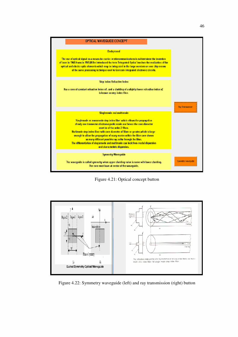
4.21 Optical concept button 46
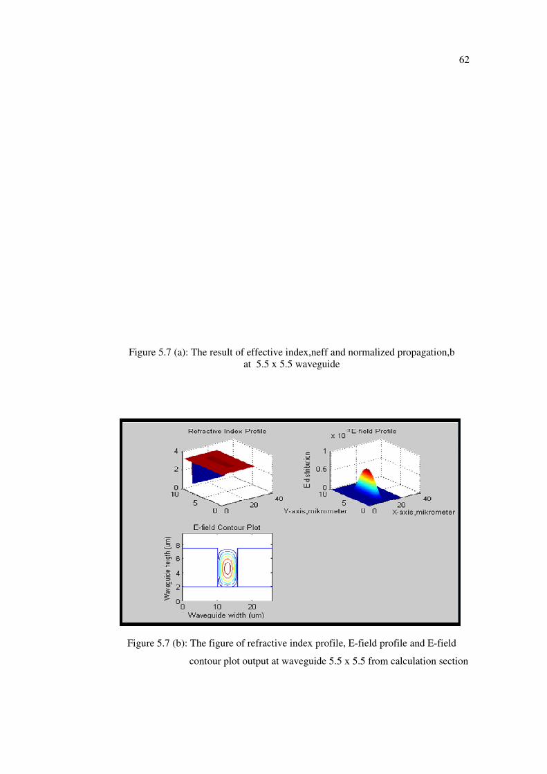
4.22 Symmetry waveguide and ray transmission button 46
4.23 Mathematical Equation button 47
4.24 Material application button 48
4.25 Figure 1 (left) and figure 2 (right) from material
application button 48
4.26 Main pages of optical devices application button 49
4.27 APD Preamplifier application button 50
4.28 Photo diode application button 50
4.29 Optical fiber application button 51
4.30 Fiber Spec Corning application button 51
4.31 Laser diode application button 52
4.32 Fabrication Process button 52
5.1 Buried optical waveguide structure plan view 56
5.2 (a) neff and b at waveguide (3 x 3) calculation result 57
(b) Figure of refractive index, E-field and E-field contour 57
5.3 (a) neff and b at waveguide (3.5 x 3.5) calculation result 58
(b) Figure of refractive index, E-field and E-field contour 58
5.4 (a) neff and b at waveguide (4 x 4) calculation result 59
(b) Figure of refractive index, E-field and E-field contour 59
5.5 (a) neff and b at waveguide (4.5 x 4.5) calculation result 60
(b) Figure of refractive index, E-field and E-field contour 60

xv
5.6 (a) neff and b at waveguide (5 x 5) calculation result 61
(b) Figure of refractive index, E-field and E-field contour 61
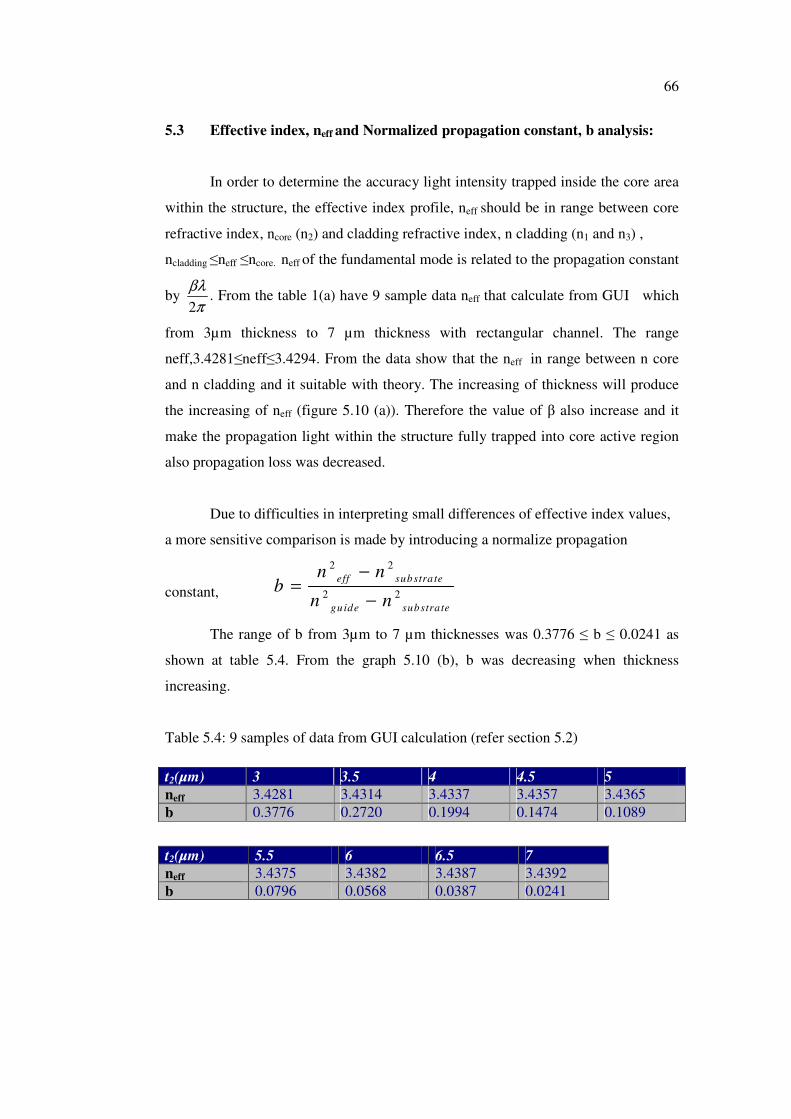
5.7 (a) neff and b at waveguide (5.5 x 5.5) calculation result 62
(b) Figure of refractive index, E-field and E-field contour 62
5.8 (a) neff and b at waveguide (6 x 6) calculation result 63
(b) Figure of refractive index, E-field and E-field contour 63
5.9 (a) neff and b at waveguide (6.5 x 6.5) calculation result 64
(b) Figure of refractive index, E-field and E-field contour 64
5.10 (a) neff and b at waveguide (7 x 7) calculation result 65
(b) Figure of refractive index, E-field and E-field contour 65
5.11 (a) Effective Index, neff graph 67
(b) Normalized propagation constant,b graph 67
5.12 Dispersion characteristic for the lowest four modes of an
anisotropic rectangular dielectric waveguide 69

xvi
LIST OF SYMBOLS
b - Normalized propagation constant
c - Speed of light; Phase velocity [m/s]
B - Magnetic flux-density complex amplitude [Wb/m2]
d - Differential
div - Divergence
D - Electric flux density [C/m2]
E - Electric field [V/m]
F - Force [kgms-2
]
H - Magnetic-field complex amplitude [A/m]
H - Magnetic field [A/m]
j - (-1)1/2
integer
J - Electric current density [A/m2]
k0 - Free space propagation constant [rad/m]
l - length [m]
m - number of modes
M - Magnetization density [A/m]
n - Refractive index
ng - Refractive index of guiding layer
ns - Refractive index of substrate layer
nc - Refractive index of cladding layer
NA - Numerical Aperture
ρ - Electric polarization density [C/m2]
Q - Electric charge [C]
T - Time [s]
TE - Transverse electric wave
TM - Transverse magnetic wave
TEM - Transverse electromagnetic wave

xvii
ϕ - Total internal reflection phase shift [rad]
V - Voltage [V]
β - Propagation constant [rad/m]
� - Electric permittivity of medium [F/m]
�0 - Electric permittivity of a free space [F/m]
�r - Relative dielectric constant of the material[F/m]
� - Angle
�c - Critical angle
� - Wavelength [m]
�0 - Free space wavelength [m]
� - Magnetic permeability [H/m]
�0 - Magnetic permeability of free space [H/m]
� - Angle in a cylindrical coordinate system
� - Angular frequency [rad/s]
∂ - Partial differential
∇ - Gradient operator
∇ . - Divergence operator
∇ x - Curl operator
∇ 2 - Laplacian operator

xviii
LIST OF APPENDICES
APPENDIX TITLE PAGE
A Source code for Buried waveguide modeling by 76
using MATLAB

CHAPTER 1
INTRODUCTION
1.1 Introduction
The use of optical signals as a means for carrier in telecommunications is
evident since the invention of laser in 1960 [2]. It was in 1969, Miller introduced the
term ‘Integrated Optics’ involves the realization of the optical and electro optic
elements which may be integrated in the large numbers on one chip means of the
same processing techniques used to fabricated integrated electronic circuits [7].
Demand for integrated optic circuits comes from the side of the light wave
communication system which required in addition to laser source, components such
as optical switches, modulators and power splitters.
Material science and fabrication technology have advanced in recent years at
an explosive rate, creating a strong interest in the possibility of extending and
replacing several functions traditionally performed by electronics with optical
devices. Day by day, new optical devices are being design, investigated and
demonstrated in research laboratories throughout the world .This development,
combined with the rapidly increasing demand for more sophiscated and widespread
telecommunication services, has put very strong pressure on the continuous
development of accurate and efficient methods for the analysis of the devices and
systems involved.

2
Dielectric waveguide are fundamental components of devices and systems both
in microwave and optics, and as such, a full understanding of how electromagnetic
waves propagate in complicated waveguide structures is essential. While in
microwaves dielectric waveguides constitute only one of the types of waveguide in
use, in optics they are practically the only form of waveguide structure. They play an
essential role in optoelectronics, being in the form of optical fibers, fiber lasers and
amplifies or in integrated optics where most devices are made from optical
waveguides of different configurations properties.
Buried optical waveguide channel are higher-index guiding layers are
selectively formed near the substrate surface by metal in diffusion, ion exchange, ion
implementation, and light/electron-beam irradiation. The buried type of 3-D
waveguide has the advantages that the propagation loss is typically lower than
1db/cm with a smooth guide surface and that planar electrodes are easily placed on
the waveguide to achieve light modulation and switching. The buried 3-D waveguide
is thus the most suitable for optical waveguide devices.
1.2 Objectives
The objective of this project is to develop simulation software for buried
waveguide structure. It also to analyst buried waveguide channel using finite
difference method and to aim for educational study on computer analysis and design.
1.3 Scope of the work
Scope of this project begins with:
i) Understanding the optical waveguide concept (buried optical waveguide).
ii) Understanding the finite difference method as a chosen method for analyzing
the waveguide.
iii) Understanding the MATLAB and GUI (graphical user interface) software as
a tool to build the simulation program and to get the accurate result.

3
1.4 Problem Statement
The propagations characteristic of optical waveguides can be calculated by
solving Maxwell’s equation, but this is difficult task and time consuming also
involve tedious or rigorous mathematically. Furthermore, Mathematical analysis not
many software available for characterization of optical waveguide and expensive
software available and also needs high speed computer such as mainframe computer.
In this project, numerical solution, finite difference method using computer (matlab
software) provide the solutions to overcome the problems and give advantages over
analytical approximation solutions. Table 1.1 shows the differentiation analysis of
optical waveguide between before software analysis and after software analysis.
Table 1.1: Differentiation before software developed and after software
developed
Before software developed After software developed
Formulation
Fundamental laws explained
briefly
Formulation
Exposition of relationship of
problem to fundamental laws
Solution
Elaborate an often complicated
method to make problem tractable
Solution
Easy-to-use computer method
Interpretation
In-depth analysis limited by time-
consuming solution
Interpretation
Ease of calculation allows holistic
thought and intuition to develop;
system sensitivity behavior can be
studied

4
1.5 Motivation of the Work
The analysis where this software simulation hopefully can be used in the
laboratory or classroom as a friendly user tool. Besides that, this analysis given
accurate, fast, effective, low cost and can be used using personal computer. The
mathematical is formulated so that with give accurate results but not involves tedious
or rigorous mathematical equation.
1.6 Methodology
Implementation and works of the project are summarized into the flow chart as
shown in Figure 1.1. Gantt charts as shown in Figure 1.2 and Figure 1.3 show the detail
of the works of the project that had been implemented in the first and second semester.
Figure 1.1: Overview Project Flow
Research an optical waveguide generally
and buried optical waveguide specifically
Study the mathematical equation with
finite difference method solution (FDM)
to get parameter and characteristic for
optical waveguide analysis.
MATLAB programming and GUI
development
Result and analysis
Thesis writting

5
Figure 1.2: Gantt chart PSM 1
n
o
ACTIVITY w
1
w
2
w
3
w
4
W
5
w
6
w
7
w
8
w
9
w
1
0
w
1
1
w
1
2
w
1
3
w
1
4
w
1
5
1 Meeting with
supervisor
2 Thesis title
confirmation
3 Making
proposal-
objective
4 Making
proposal-
Methodology
&
Approaches
5 Making
proposal -
Expected
Result
6 Complete and
submit PSM1-
1 form
7 Create The
Gantt Chart
8 Study optical
waveguide &
buried
waveguide
9 Study
Maxwell
equation and
finite
difference
method
10 Study Matlab
simulation
and GUI
11 Preparation
for PSM 1
seminar
12 PSM 1
seminar
13 Writing final
report of
PSM1
14 Submit final
report PSM 1

6
Figure 1.3: Gantt Chart for PSM 2
N
O ACTIVITY W
1
W
2
W
3
W
4
W
5
W
6
W
7
W
8
W
9
W
1
0
W
1
1
W
1
2
W
1
3
W
1
4
W
1
5
1 Meeting with
supervisor
2 Thesis writing-
chapter1
(introduction)
3 Thesis writing-
chapter2
(literature review)
4 Thesis writing-
chapter3
(mathematical
analysis)
5 Submit the progress
project form2-0
6 Run MATLAB
simulation and
build GUI
7 Result and analysis
8 Thesis Writing-
chapter4
(MATLAB and
GUI development)
9 Thesis writing-
chapter5
(result and analysis)
10 Thesis writing-
chapter6
(conclusion and
recommendation)
11 Submit a brief
project formPSM2-
1
12 PSM2 –TOP
Exhibition (
seminar and demo)
13 Final check and
submit final draft
14 Submit the
hardcopy and the
softcopy

7
1.7 Structure of thesis
This thesis consists of six chapters including this introduction follow the
university thesis standard. In second chapter present overview of an optical
waveguide structure. Dielectric waveguides are the structures that confine and guide
the light in the guided-wave devices and circuits of the integrated optic in a region of
higher effective index that surrounding media. Buried structure waveguide, which
are integrated optical component and as well as methods for analyzing the
electromagnetic fields. The analytical methods for describing propagation along
waveguides using the single modes are presented.
Analysis of optical waveguide will be present at chapter three. Based on the
Maxwell equations, a set of scalar wave equations governing the propagation of E-
field and H-field in the straight waveguides are derived. The propagation
characteristic of buried waveguide with straight and bending structure have been
investigated at wavelength of 1.55 micrometer. Then, an optical waveguides have
been analyzed using the numerical method based on finite difference approach.
Meanwhile the chapter 4 focused on propagation characteristic and the field
of the guided modes can be calculated very efficiently on a personal computer with
modest computational time. Three dimensional (3D) figure plot and contour profile
field in waveguide using MATLAB software will be determine as result analysis.
Beside that chapter 5 present on the analysis of the result and discussion which
analysis the performance in terms of the waveguide modes and its confinement
depends on parameters that include dimension on the core waveguide and
relationship between core and the cladding refractive index will be an optimized.
Finally, the main contributions are summarized in chapter six to conclude this thesis.

CHAPTER 2
OPTICAL WAVEGUIDE
2.1 Introduction
The increasing complexity of modern devices in optics rules out accurate
analytical treatment and so it has maintained a critical demand for accurate and
efficient computer modeling. Computer modeling techniques that allow an accurate
simulation of the behavior of real devices have become increasingly more common
and popular with the availability of cheaper and ever more powerful computer
resources. Optical waveguide had been used widely and becoming fast as a major
reason in development of optical circuit that gives more advantages than
conventional way. Thus, the analysis and modeling optical waveguides had been
given special attentions by researchers as important step before waveguides can be
practically used.
2.2 Background
The rapid development in fields such as fiber optics communication
engineering and integrated optical electronics have expanded the interest and
increased expectations about guided-wave optics, in which optical waveguides play a
central role. Optical waveguides for optical fibers and optical integrated circuits
utilize a wave phenomenon that traps the light locally and guides it in any direction,

9
although their propagation lengths differ greatly [2]. In order to develop new optical
communication systems or optical devices, we need to fully understand the principle
of optical guiding, while obtaining accurate quantitative propagation characteristic of
waveguides and utilizing them effectively in actual design. The generally meaning
optical waveguide is the��physical structure that guides electromagnetic waves in the
optical spectrum. Common types of optical waveguides include optical fiber and
rectangular waveguides. Channel of optical waveguide such as buried, ridge, rib, slab
and surface embedded. It is used as components in integrated optical circuit or as the
transmission medium in local and long haul optical communication system.
2.3 Buried Optical Waveguide channel
A buried waveguide is made by modifying the properties of the substrate
material so that a higher refractive index is obtained locally. Most fabrication process
results in a weak, graded index guide buried just below the surface. Diffusion is often
used to fabricate this type of guide. For example Titanium metal can be diffused into
Lithium Niobate substrates, by putting the metal strip about 10000A thickness follow
by higher temperature (approach 10000
C) for three to nine hours. This is known as
Ti:LiNbO3 [5] process as shown in figure 2.1. The additional of that metal act as an
impurities that cause a change of the refractive index.
Figure 2.2 illustrate configuration of a dielectric channel waveguide (buried). The
surrounded channel with the refractive index n1
greater than n2, n3
, and n4, is called
the core, or, the guiding channel. And the other areas with the lower refractive
indices are called the claddings, or, index buffering layers. This whole structure is
usually built on a substrate, such as silicon wafer, silica, glass or PC board.
In the structure shown in Figure 2.2, n2, n
3, and n
4 can be the same, which
makes the structure a buried channel waveguide. n2
and/or n3
may be air. Depending
on the geometric structure, refractive indices, and wavelength, certain modes can be
supported and light can therefore propagate through the waveguide [4].
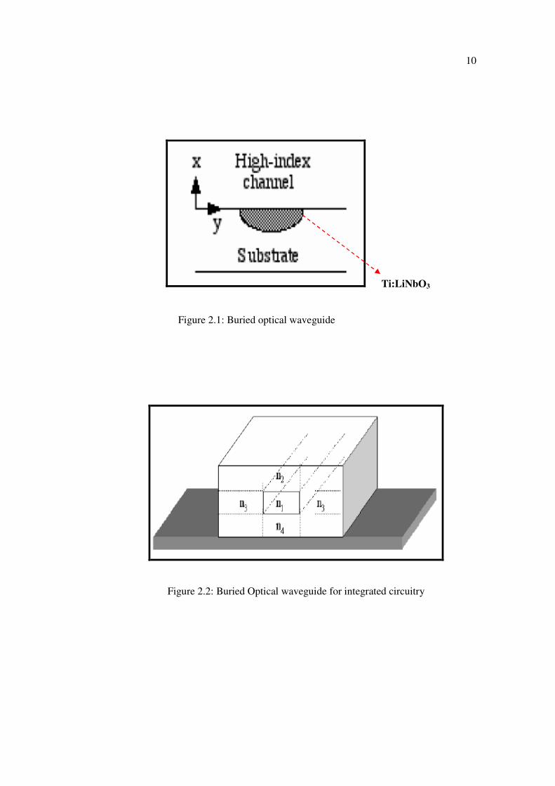
10
Ti:LiNbO3
Figure 2.1: Buried optical waveguide
Figure 2.2: Buried Optical waveguide for integrated circuitry

11
2.4 Types of Waveguides
Optical waveguides can be classified according to their:
• geometry (planar, strip, or fiber waveguides)
• mode structure (single-mode, multi-mode)
• refractive index distribution step or gradient index)
• material (glass, polymer, semiconductor)
2.4.1 2-D Optical waveguides
Waveguides that trap the light only in the direction of thickness are called 2-
D optical waveguides or slab waveguides. It can be stepped or graded optical
waveguides based on distribution of its refractive index. Figure 2.3 shows the
simplest three layer waveguide structure. It is the simplest, most basic waveguide
structure.
Here, nf, ns and nc represent the refractive indexes of the thin film, substrate,
and upper cladding, respectively. When the upper cladding is air, as in most cases,
nc=1. This type of optical waveguide is called a three layer dielectric waveguide or
an asymmetric slab waveguide. The relationship among the refractive indexes is
nc<ns<nf , and the light is trapped inside the thin film [1] . In the case of rectangular
waveguide geometry the presence of the air-semiconductor interface also reduces the
symmetry, to only x-direction, as shown in Fig.2.5.
The cross-sectional profile of a buried waveguide with rectangular core cross
section, lying near to the air-semiconductor boundary is given in Fig.2.6. The
waveguide of core refractive index n1, width 2W and thickness 2H, is buried in a
semiconductor of refractive index n2 at a depth D below the air boundary. The cross
section is divided in two regions: region I which encloses the rectangular waveguide
core, ( | x | < W) and region II ( | x | > W) [6] .

12
y
nc= cladding refractive index
z
nf =film refractive index
ns=substract refractive index
Figure 2.3: Three layer dielectric waveguide
Figure 2.4: 2-D optical buried waveguide channel
Figure 2.5: Planes of symmetry of (a) deeply buried waveguide, (b) shallowly
Buried waveguide

13
Figure 2.6: The cross-sectional profile of the air-clad buried waveguide
2.4.2 3-D Optical Waveguides
A 2-D optical waveguides can trap light in the direction of the thickness (y
direction), but allows light to spread in the horizontal direction(x direction). In order
to facilitate the construction of optical integrated circuits, various types of 3-D
optical waveguides as shown in fig.2.7, or optical channel waveguides, which trap
the light in both x and y directions, have been devised.
Figure 2.7: 3-D Buried waveguide channel

14
2.5 Buried Optical Waveguides Application
The buried optical waveguide is a very important component and suitable for
integrated optical technologies, finding widespread and significant inferometers,
splitters, and switches and also as an optical interconnects such as bends and
junction. The higher index guiding layers are selectivity formed near subtracts
surface by metal in diffusion, ion exchange, on implantation and light beam
radiation. The buried type of channel waveguide has the advantages that that the
propagation loss in typically lower in 1 dBm with smooth surface. It’s usually
suitable for bend waveguide with small curvature radii due to its characteristic that
strongly transverse confinement of scattering loss due to waveguide wall roughness
[3].
An optical waveguide that is uniform in the direction of propagation, as
shown in Fig.2.1 is the most basic type of waveguide, but this alone is not sufficient
for construction of an optical waveguides is placed on the substrate to construct an
optical circuit with desired features. Corner –bent waveguides, S-shaped waveguides,
and bent waveguides are used to change the direction of the light wave. Tapered
waveguides are used to change the width of waveguides; branching waveguides and
crossed waveguides are used for splitting, combining, and interference; and optical
waveguide directional couplers and two mode waveguide couplers are used for
coupling. Waveguide gratings, with a periodic structure in the direction of
propagations, play many important roles in the optical integrated circuit, such as
wavelength filter, mode converter, reflector, resonator, demultiplexer, etc.
Waveguide gratings are also used widely as a laser element, such as a distributed
Bragg reflector (DBR) laser or a distributed feedback (DFB) laser.

15
2.5.1 Fabrication process.
Semiconductor device fabrication is the process used to create chips, the
integrated circuits that are present in everyday electrical and electronic devices. It is
a multiple-step sequence of photographic and chemical processing steps during
which electronic circuits are gradually created on a wafer made of pure
semiconducting material. Silicon is the most commonly used semiconductor material
today, along with various compound semiconductors.
The entire manufacturing process from start to packaged chips ready for
shipment takes six to eight weeks and is performed in highly specialized facilities
referred to as fabs [ ]8 .
Figure 2.8: NASA’s Glenn Research Center (fabrication process)

16
2.6 Optical Waveguide Analysis techniques
The propagation characteristics of optical waveguides can be calculated by solving
Maxwell’s equations but this is not easy task. There are many reasons that optical
waveguide analysis is difficult; some of the major reasons are listed below:
1) Optical waveguides have complex structures.
2) The general propagation mode is the hybrid mode.
3) Some optical waveguides have an arbitrary refractive index distribution (graded
Optical waveguides), as in doped optical waveguides and non –uniform core
optical fiber.
4) The range of electromagnetic field distribution is open, or infinite.
5) Anisotropic materials and nonlinear optical materials are used to increase the
range of performance.
6) Materials with a complex refractive index, such as semiconductors and metals,
are used. To overcome these difficulties, various methods have been developed
for the analysis of optical waveguides. Such methods may be roughly classified it
analytical approximation solutions and numerical solutions using computer.

17
2.6.1 Analytical Approximation Solutions for Optical Waveguides
An exact analytical problem solution can be obtained for stepped 2-D optical
waveguides and stepped optical fibers .if, however, the waveguide has an arbitrary
refractive index distribution and exact analysis is no longer possible. Therefore,
various types of analytical approximation solutions have been developed for 2-D
optical waveguides in which the refractive index changes gradually in the thickness
direction, and for optical fiber whose refractive changes gradually only in the radial
direction.
In the case of 3-D optical waveguides for optical integrated circuits and non
axisymmetrical optical fiber, hybrid mode analysis is required to satisfy the boundary
conditions, even if the individual materials that constitute the waveguide are
homogenous. However, the analytical approximation solutions developed for these
optical waveguides generally do not treat them as hybrid mode, and therefore, the
accuracy of the solution deteriorates near the cutoff frequency. The Marcatili method
(MM) and the effective index method (EIM), known as typical analytical
approximation solutions for 3-D optical waveguides, and the equivalent network
method (ENM), which enables hybrid-mode analysis [9].

18
2.6.2 Numerical solutions for Optical Waveguides.
Numerical solutions can be grouped into the domain solution, which includes
the whole domain as the operational area, and the boundary solution, which includes
the whole domain as the operational area, and the boundary solution, which includes
only the boundaries as the operational area. The former is also called a differential
solution, and the latter, an integral solution. The domain solutions include the finite
element method (FEM), finite difference method (FDM), variation method (VM) and
multilayer approximation method(BEM), point matching method (PMM) and mode-
matching method(MMM).For the analysis of graded optical waveguides, the use of
boundary solutions is difficult. The finite difference method (FDM) is a simple
numerical technique used in solving problem that uniquely defined by three things:
1) A partial differential equation such as Laplace’s or Poisson’ equation
2) A solution region
3) Boundary and/or initial conditions
A finite difference method to Poisson’s or Laplace’s equation, for example, proceeds
in three steps:
1) Dividing the solution region into a grid of nodes
2) Approximating the differential equation and boundary conditions by a set of
Linear algebraic equations (called difference equations) on grid points within
solution region.
3) Solving this set of algebraic equations.

CHAPTER 3
MATHEMATICAL ANALYSIS
3.1 Overview of numerical method
Numerical methods solve Maxwell’s equations exactly and the results the
provide are often regarded as benchmarks. Integrated waveguides, by contrast, are
usually rectangular structures which confine the light in both directions. Because
they do not have planar or cylindrical symmetry, the eigenmodes of these structures
cannot be computed analytically. Instead, numerical techniques must be used to solve
the eigenvalue equations. There are many different numerical techniques for solving
partial differential equations such as the Finite Difference (FD), Finite Elements (FE)
and Finite Difference Beam Propagation (FDBPM) methods which are robust,
versatile and applicable to a wide variety of structures. Unfortunately, this is often
achieved at the expense of long computational times and large memory requirements,
both of which can become critical issues especially when structures with large
dimensions are considered or when used within an iterative design environment.

20
3.2 Finite Difference Methods (FDM)
The FD method is one of the most frequently used numerical techniques
[6].Its application to the modeling of optical waveguides dates from early eighties,
originally evolving from previous FD models for metal waveguides [8]. The FD
method discretisizes the cross-section of the device being analyzed and is therefore
suitable for modeling arbitrarily shaped optical waveguides which could be made out
of isotropic homogeneous, inhomogeneous, anisotropic or lossy material. In the finite
difference technique, differential operators are replaced by the difference equations,
as example, the first derivative of a function f (x) could be approximated as
( ) ( )'( )
f x x f xf x
x
+ ∆ −≈
∆ (1)
This is a very intuitive approximation and mostly elementary calculus define
the fist derivative of a function to be just such a finite difference in the limit that
x !"0 .This equation (44) fails entirely if the function f (x) is discontinuous in the
interval x !"x #" x .Maxwell equations predict that the normal component of the
electric field are discontinuous across abrupt dielectric interfaces. Therefore in order
to develop an accurate model for eigenmodes of an optical waveguide, it must
construct a finite difference scheme which accounts for the discontinuities in the
eigenmodes [7].
The essence of the FD is to map the structure onto a rectangular mesh [8] [9]
as example shown in Figure 3.3illustrates a typical finite difference mesh for ridge
waveguide, allowing for the material discontinuities only along mesh lines. The
refractive index profile has been broken up into small rectangular elements or pixels,
of size x $" y .Over each of these elements, the refractive index is constant.
Thus, discontinuities in the refractive index profile occur only at the boundaries
between adjacent pixels. Because of the index profile is symmetry about the y -axis,
only half of the waveguide needs to be included in the computational domain [7].

21
The computational window must extend far enough outside of the waveguide
core in order to completely encompass the optical mode. The finite difference grid
points, which the discrete points at fields are sampled, are located at the centre of
each cell. Some finite difference schemes instead choose to locate at the grid points
at the vertices of the each cell rather than at the centre. This approach works well for
finite difference schemes involving the magnetic field H which is continuous across
all the dielectric interfaces. However, the normal component of the electric field E is
discontinuous across an abrupt dielectric interface, may leads to an ambiguity if the
grid points are placed at cell vertices. Figure 3.4 shows that the possible ways of
placing nodes on the mesh with a constant refractive index [10] and that node can be
associated to maximum of four different refractive indices [9].
Figure 3.1: A typical finite difference mesh for an integrated waveguide. The
refractive index profile n(x, y) has been divided into small rectangular cells over
which n(x, y) is taken to be constant.
Figure 3.2: Locating nodes (a) on centre of a mesh cell or (b) on mesh points.

22
We will begin by deriving the finite difference equations for the scalar
eigenmode approximation. Recall in this approximation nave been replaced by a
single scalar eigenmode equation for one of the transverse field components denoted
%(x, y) as equation (49).This approximation is valid for “weakly-guiding”
waveguides in which the refractive index contrast is small.
2 2
2 2
02 20k
x yβ
� �∂ ∂+ + Φ − Φ =� �
∂ ∂� � (2)
Or
22 2
2 20
Tk
x y
� �∂ ∂+ Φ + Φ =� �
∂ ∂� � (3)
The parameter kT determines the propagation constant &" through,
2 2 2
Tk ω µε β= − In order to translate this partial differential equation into a set of
finite difference equations, we must approximate the second derivatives in terms the
values of %(x, y) at surrounding grid points as
(4)
This approximation can be derived by performing a second order Taylor expansion
of field about the grid point under consideration, P. With this notation, the central
difference approximations of the derivatives of %"at the ( i, j ) th node are
2
( 1, ) 2 ( , ) ( 1, ),
( )xx
i j i j i ji j
x
Φ + − Φ + Φ −Φ ≈
∆ (5)
2
( , 1) 2 ( , ) ( , 1),
( )tt
i j i j i ji j
t
Φ + − Φ + Φ −Φ ≈
∆ (6)
''
2
( ) 2 ( ) ( )( )
f x x f x f x xf x
x
+ ∆ − + − ∆≈
∆

23
The differential of scalar, semivectorial or vector polarized wave equation is then
approximated, usually with a five point FD form in terms of the fields at the nodes of
the mesh point. For improved convergence more accurate difference forms can be
used [6].Taking into account the continuity and discontinuity conditions of the
electric and magnetic field components at the grid interface the eigenvalue problem
becomes of the form
[ ] 2A βΦ = Φ
(7)
where 'A ! is a band matrix which is symmetric for scalar modes [6] or non
symmetric for semivectorial[10][13] and vector modes. "! , the modal propagation
eigenvalue and #!is the eigenvector representing the modal field profile. Whilst FD
method is in principle straightforward to implement, numerical modeling of the open
boundaries, typical of optical waveguides needs care. The problem is overcome by
either (a) enclosing a structure in a sufficiently large rectangular box which does not
disturb the penetration of the field and on which the zero field condition is imposed
or (b) imposing an open boundary or matched boundary condition on the box sides
for example by assuming exponential decay of the field in the outward normal
direction. However when the device operates near cut-off the size of the box for both
cases has to be sufficiently large to allow for substantial penetration of the field into
the substrate. The accuracy of the method therefore depends on the mesh size, the
assumed nature of the electromagnetic field and the order of the FD scheme used. In
this projects work open boundary or matched boundary condition and non-uniform
meshes have been proposed such that a finer mesh is applied in the region where the
field changes rapidly and a coarser mesh for regions where field is stationary to make
the FD method more flexible for modeling of large and complex geometries The
variational method is used to establish the eigenvalues and the eigenvectors and the
successive over relaxation method (SOR)[11]]has been considered as the
acceleration factor as an improvement that speed the convergence process.

24
3.3 Numerical methods solve Maxwell’s equation exactly
The basic formulation that governs the propagation of light in the optical
waveguide isa Maxwell’s equations that consist of the following [10]:
. 0
. V
d BX E
d t
d DX H J
d t
B
D ρ
−∇ =
∇ = +
∇ =
∇ = (8)
Where:
E : Electric field intensity
H : Magnetic field intensity
D : Electric field
B : Magnetic field density
Vρ : Electric charge density
J : Current density
Assuming that the waveguide is made of isotropic, homogeneous and free of source
medium, Equation (8) will become:
. 0
. 0
d BX E
d t
d DX H
d t
B
D
∇ = −
∇ =
∇ =
∇ = (9)

25
Manipulating Equation (9) will produce a so-called Helmholtz wave equation that
adequately describes the propagation of electromagnetic wave. The wave equation
for the electric field can be presented as:
22
2
d EE
d tµ ε∇ = (10)
Considering a y-polarized TE mode which propagates in the z-direction and � as a
propagation constant in longitudinal direction will then yield:
2 2
2
2 2
y y
y y
d E d EE E
dx dyβ ϖµε+ − =−
(11)
Taking 2k ϖ as the total propagation constant which combine the horizontal and
vertical part will then produce:
222 2
2 2( ) 0
y
y
d Ed Eyk E
dx dyβ+ + − =
(12)
Knowing that k is a multiplication of free space propagation constant, k0 and
refractive index, n for respective layer, Equation (12) can be written in the form of:
222 2 2
02 2( ) 0
y
y
d Ed Eyk n E
dx dyβ+ + − =
(13)
Equation (6) is the eigenfunction that need to be solved for determining the
eigenvalue of β and TE field distribution throughout the medium of interest.

26
In the application of finite difference method to solve Equation (6), the E
field and the refractive index, n, is considered to be a discrete value at respective x-
and y coordinate and bounded in a box, which represent the waveguide cross section.
The box is divided into smaller rectangular area with a dimension of x and y in
x- and y- directions respectively [8]. Brief description is given in Figure 1, where the
waveguide cross section area is divided into M × N grid lines, which corresponds to
the mesh size of x and y .
Considering the Ey having component in x and y direction E(x,y), Taylor’s expansion
is applied to Equation (13) where the differential components are obtained as
follows:
2
2 2
2
2 2
( 1, ) ( 1, ) 2 ( , )
( , 1) ( , 1) 2 ( , )
d E E i j E i j E i j
dx x
d E E i j E i j E i j
dy y
+ + − −=
∆
+ + − −=
∆
(14)

27
Combining Equations (6) and (7) will produce a basic equation for obtaining the
electric field:
2
2
2
22
2 2 2 2
0
( 1, ) ( 1, ) ( ( , 1) ( , 1))
( , )
2 1 ( ( , ) )
xE i j i j E i j E i j
yE i j
xx k n i j
yβ
� �∆+ + − + + + −� �
∆� �=� �� �∆� �+ − ∆ −� �� �∆� �� �
(15)
Where i and j represent the mesh point corresponding to x and y directions
respectively. If Equation (13) is multiplied with y E and operating double integration
towards x and y, it will yield:
2 2
2 2
02 2
2
2
y y
y y
y
d E d EE k n E dxdy
dx dy
E dxdyβ
� �� �+ +� �� �� �� �
� �� �=
��
�� (16)
Equation (9) is called Rayleigh Quotient. Further application of finite difference
method and trapezoidal rule to Equation (16) shall then produce:
(17)
Equation (17) is obtained by applying Dirichlet boundary condition which states the
E (i, j) = 0 at the boundary. Initial value of E (i, j) = 1 is set for other points. In order
to speed up the process, a successive over relaxation (SOR) parameter [8, 9], C
introduced to Equation (15), which states that the iteration will converge faster for C

28
between 1 and 2. According to [9], taking SOR parameter into consideration will
modify Equation (15) to be:
(18) Alternate usage of Equations (17) and (18) for the decided tolerance will produce the
final value of and the TE field distribution for the entire waveguide cross section.
neff of the fundamental mode is related to the propagation constant by 2
βλ
π. Due to
difficulties in interpreting small differences of effective index values, a more
sensitive comparison is made by introducing a normalized propagation constant [4],
2 2
2 2
eff substrate
guide substrate
n nb
n n
−=
− (19)
This mathematical calculation will be developed into computer programming using
Matlab R2006a and the result can be used to plot graph.

CHAPTER 4
MATLAB AND GUI DEVELOPMENT
4.1 Introduction of MATLAB software
MATLAB was mainly designed to solve any type level of mathematical
problem for analysis purpose. Beside that, good capability of the software to deal
with various useful problems concerned with the modeling, evaluation and
optimization of the 3D waveguide structure performance. The Figure 4.1 shows that
how the MATLAB works to develop software for optical waveguide simulation and
the overall methodology of project will be given by flow chart in Figure 4.1.
4.1.1 Basic MATLAB features
MATLAB provides a logical solution to evaluate a number of commands or
wish to change value of one or more variables in one prompt. It allows placing
MATLAB commands in a simple text file and then telling MATLAB to open the file
and evaluate commands exactly. These files are called script files or simply M-files.
The term M-files recognizes the fact that script file name must end with the
extension.m example, amp1.m to create a script M-files on a personal computer,
choose New from the File menu and select M-File. This procedure brings up a text
editor window where you enter MATLB commands. On other platforms, it is
convenient to open a separate terminal window and use your favorite text editor in
that window to generate script M-File. Script files are also convenient for entering

30
large arrays that may, for example, come from laboratory measurements. By using a
text editor to enter one or more arrays, the editing capabilities of the editor make it is
easy to correct mistakes without having to type the whole array in again.
The utility of MATLAB comments is readily apparent when using script files
as show in M-file.m file. Comments allow you to document the command found in
script file so that they are not forgotten when viewed in future. After running script
files, the results of the command are displayed in the Command Window with
variable identified. The plotting result for responses of command script files will be
display on Figure. waveguides. An example of computational and software
development step is as shows in Figure 4.4.You can see the MATLAB source code
simulation propagation APPENDIX A.

31
Figure 4.1: The flow chart show that how MATLAB work

32
YES
NO
Figure 4.2: The flow chart of the programming process
Preliminary studies Topic research and
info gathering
Mathematical equations for derivation and
numerical method
TASK: Development program MATLAB
in 3 D and simulation-model waveguide
structure (buried)
Test and run
Developed with Graphical User Interface
(GUI)
Trouble-shoot and
reprogramming
Update and upgrade
End
Success?

33
4.2 Basic Graphic User Interface (GUI)
The MATLAB programming environment is flexible and there are many
ways to achieve the same functionality, especially in GUI programs. There are many
advantages when we use the GUI programs, as an example, we can develop a simple
graphical application, demogui. This application will display a window with an
editable text field containing a number (initially "1") and two buttons which will
allow us to increment or decrement this number by 1. The design of the user
interface and the functionality of the application are often the most difficult aspects
of GUI programming; the programming itself is not that hard. All functionality is
programmed into a single m-file with a single argument which serves as a function
selector. The various operations are to be implemented by calling this m-file with
different values for the selector. The initialization of the application is achieved by
calling demogui with no arguments. In Matlab, GUI can be designed using GUIDE.
GUIDE is the MATLAB graphical user interface development environment. It
provides a set of tools for creating graphical user interfaces (GUIs). It use to simplify
the process of designing and building GUIs.
4.2.1 User of GUIDE
1) Lay out the GUI
It can lay out a GUI easily by clicking and dragging GUI components such as
panels, buttons, text fields, sliders, menus and so on. The GUIDE stores the
GUI lay out in a FIG-file.
2) Program the GUI
GUIDE automatically generates an M-file that controls how the GUI
operates. M-file initializes the GUI and contains a framework for the most
commonly used callbacks for each component (the commands that execute

34
when a user clicks a GUI component). We can edit the code of callbacks in
M-file Editor.
4.2.2 Starting GUIDE
The GUIDE can be start by typing ‘guide’ at the MATLAB command
window. Then, GUIDE Quick Start dialog box will be displayed. In Matlab, there are
10 styles of Matlab Uicontrol objects. As example, Push Buttons, Toggle Buttons,
Check Box, Radio Button, Editable text, List Box, Pop-up Menu, Slider, Frame and
Static Text.
4.3 ‘My GUI’ Concept
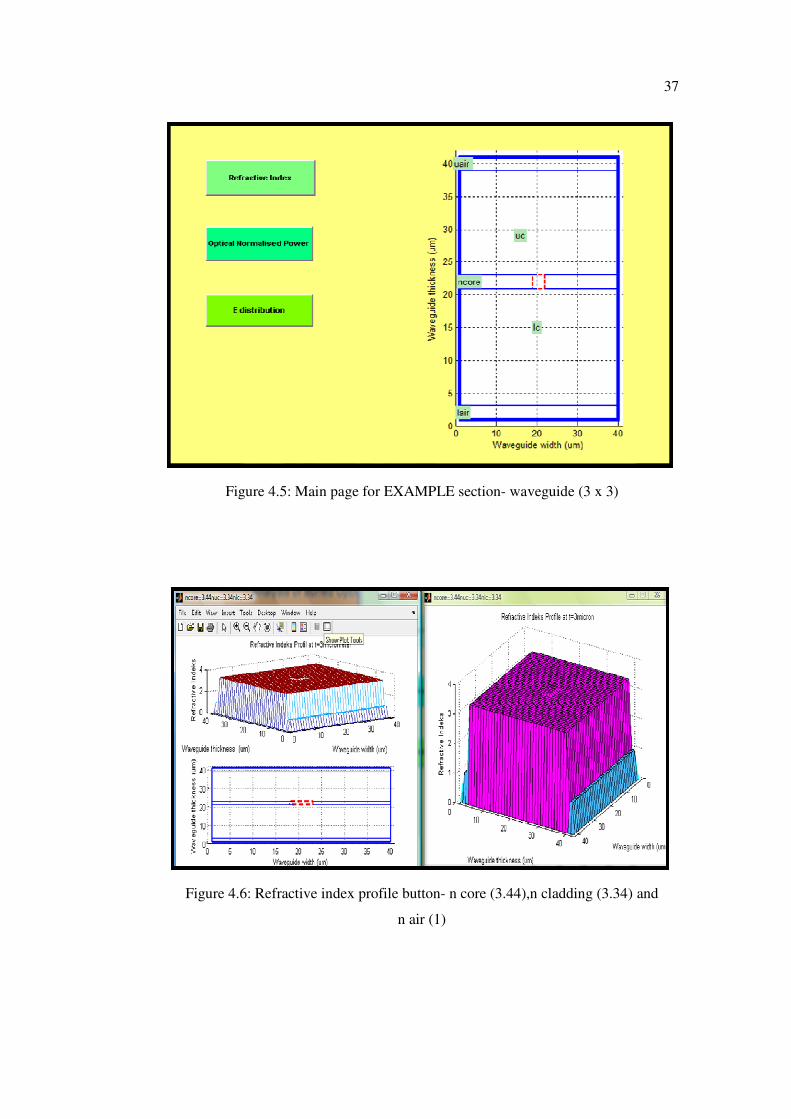
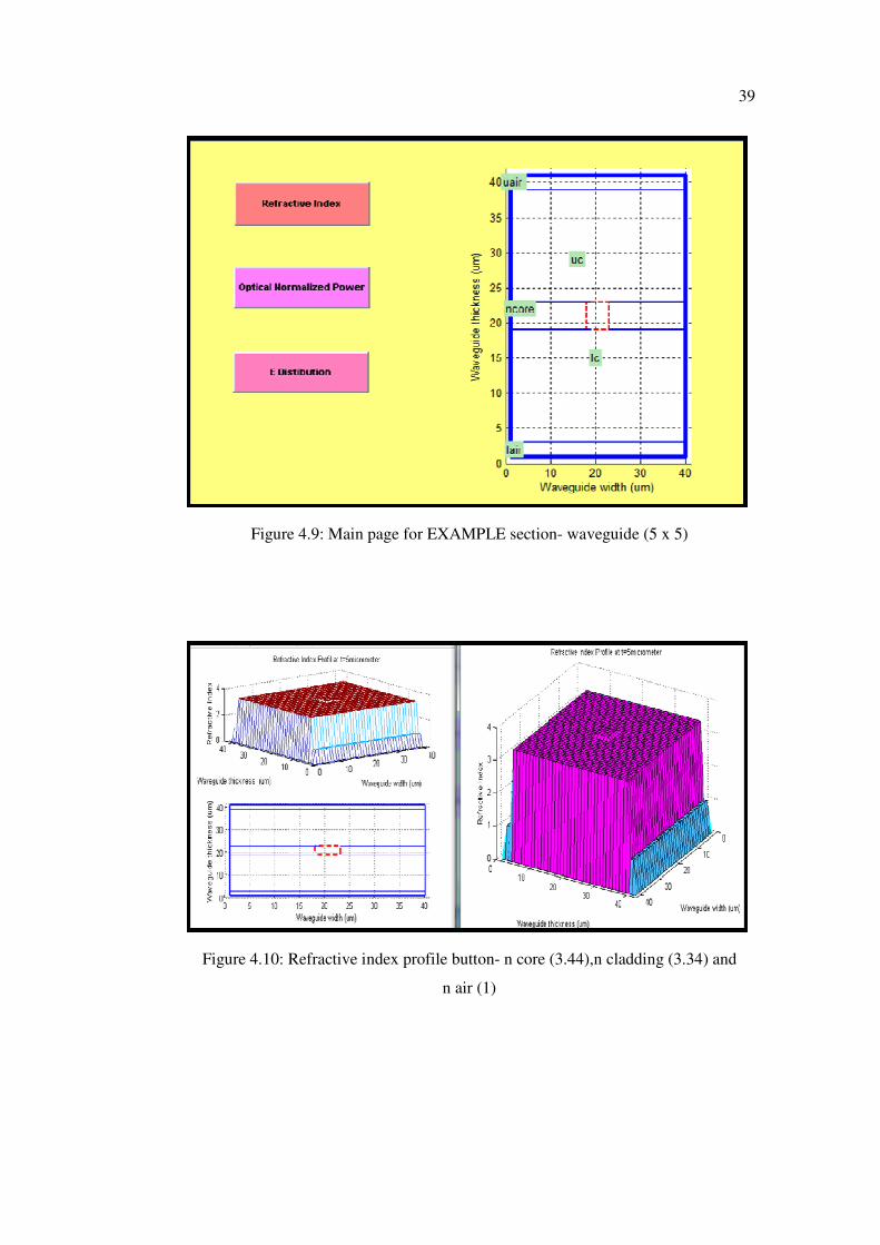
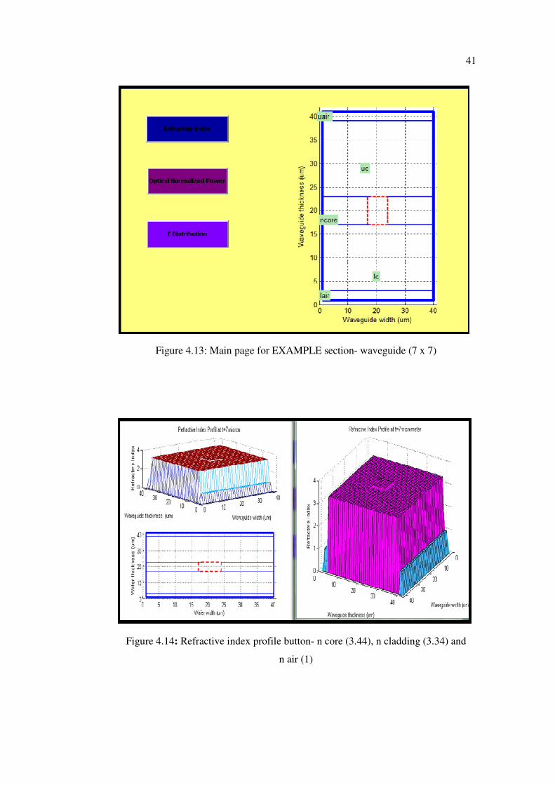
‘My GUI’ name will be given of this project. From main page,user can
explore many section of Buried optical waveguide with just click the button. The
EXAMPLE section have 3 subsection which waveguide 3x3, waveguide 5x5,
waveguide 7x7.The objective to build this section to show the 3D figure of refractive
index, optical normalized power and e-field profile with influence of air and larger
thickness and width value.Next section is CALCULATION section, user just put the
parameter of core thickness and core width,the result of effective index and
normalized propagation constant will out. ANALYSIS section show the graph of
effective index and normalized propagation from CALCULATION section.Last
section is APPLICATION which it will give briefing and idea to the user about
generally application and data sheet of optical waveguide.In APPLICATION section
have 4 subsection such as optical concept, mathematical equation, material/substrate
application and optical devices (APD Preamplifier, PIN Photo Diode, Optical fiber,
Fiber Spec Corning, Laser Diode and Fabrication Process). Figure 4.3 shows the
overview plan of ‘My GUI’ concept and figure 4.4 – figure 4.33 shows the ‘My
GUI’ output and pop up with friendly user.

35
Figure 4.3: Overview plan of ‘My GUI’

36
Figure 4.4: Main Page of ‘My GUI’
37
Figure 4.5: Main page for EXAMPLE section- waveguide (3 x 3)
Figure 4.6: Refractive index profile button- n core (3.44),n cladding (3.34) and
n air (1)

38
Figure 4.7: Optical Normalized Power button - 0.7010
Figure 4.8: E-field profile button
39
Figure 4.9: Main page for EXAMPLE section- waveguide (5 x 5)
Figure 4.10: Refractive index profile button- n core (3.44),n cladding (3.34) and
n air (1)

40
Figure 4.11: Optical Normalized Power button - 0.6500
Figure 4.12: E-field profile button
41
Figure 4.13: Main page for EXAMPLE section- waveguide (7 x 7)
Figure 4.14: Refractive index profile button- n core (3.44), n cladding (3.34) and
n air (1)

42
Figure 4.15: Optical Normalized Power button - 0.6110
Figure 4.16: E-field profile button

43
Figure 4.17: Calculation part in ‘My GUI’

44
Figure 4.18: Analysis section in ‘My GUI’
Figure 4.19: neff graph (left) and b Graph (right)

45
Figure 4.20: Main page of application in ‘My GUI’
46
Figure 4.21: Optical concept button
Figure 4.22: Symmetry waveguide (left) and ray transmission (right) button

47
Figure 4.23: Mathematical Equation button

48
Figure 4.24: Material application button
Figure 4.25: figure 1 (left) and figure 2 (right) from material application button

49
Figure 4.26: Main pages of optical devices application button

50
Figure 4.27: APD Preamplifier application button
Figure 4.28: Photo diode application button

51
Figure 4.29: Optical fiber application button
Figure 4.30: Fiber Spec Corning application button

52
Figure 4.31: Laser diode application button
Figure 4.32: Fabrication Process button

CHAPTER 5
RESULT, ANALYSIS AND DISCUSSION
5.1 Result Process
Using MATLAB software it will be design 3D dimensional structure of
buried waveguide channel and it will be user friendly for waveguide analysis on
computer modeling. In This project to get the finally result must have two stage, first
stage is MATLAB M-file result and second stage is GUI result.
5.1.1 First stage
The software consists of three main components which are inputs parameters,
processing data and output. The input parameters for the software can be divided into
two categories as shown in table 4.1. First categories of inputs are required by the
algorithm of the Finite Difference Method. Second categories of inputs are used to
control the sequence of the application. Data from input parameters will be used for
calculating the output or to be transformed to other form of data.

54
Table 5.1: Categories of input
Categories Of Inputs
Types of Inputs Control Input
1)Rectangular waveguide dimension =
w x t
2)Refractive index , n core = 3.44,
n clad = 3.34
3)Mesh Size, dx = 0.01,dy =0.01
4)Wavelength = 1550 nm
Tolerance = 0.0001
Table 5.2: Processing Data
Input Processing data Output
1)Waveguide dimension:
thickness of cladding,
guiding and core
layer
2) Mesh size
Index = width / mesh size
Size of mesh index
Such as N x M
Table 5.3: Final Output
Input Output
1)Electric field distribution
2)Propagation constant,�
1)Effective Index, neff
2)Normalized Constant
3)Three Graph:
i) Refractive Index Distribution
ii) 3D field distribution
iii) Contour plot of field distribution

55
5.1.2 Second stage
After done with debugging and testing the code in M-file editor, graphical
user interface (GUI) was applied to the code.GUI Builder is used for this purpose.
The GUI has three sections as shown in the Figure 4.7.The Buried structure figure is
used as a reference for the user to put the input parameters for the simulation. The
input parameters are divided into three section; Waveguide dimension, Refractive
index and Analysis setting. CALCULATE button on the below right of the GUI need
to be pushed to start the simulation. The output for the simulation; Effective index
and Normalized Propagation Constant will be shown on the same GUI. A window
containing three figures; 3D plot contour, refractive index profile and field
distribution profile also will pop up after the simulation.
5.2 Calculation result and Buried optical waveguide figure presentation
Figure 5.1 - 5.9 shows the waveguide structure of buried waveguide
channel.n1 is the refractive index upper cladding, n2 is the refractive index core and
n3 is the refractive index lower cladding. Meanwhile t1 represent of upper cladding
thickness and w stand for core width. This project focused on buried square channel
that symmetrical and straight waveguide. Have a little bit assumption for the
calculation which assumes no air at the waveguide, t1 and t3 was fixed at 2
micrometer and assume n upper cladding (n1) and n lower cladding (n3) equal to
3.34. Beside that n core (n2) equal to 3.44 also assume lambda wavelength is 1.55
micrometer.
Meanwhile, the figure also shows the refractive Index profile, E-field contour
plot with difference thickness. The value of E-field profile not constant and not
proportional because the value depends on core thickness and core width. Its mean
difference thickness and width influencing the optical normalized power and light
propagation in the waveguide. Contour plot shows where light wave propagate and
E-field radiated in waveguide either in core region or outside core region. The small

56
difference refractive index among core and cladding can give better performance of
electromagnetic field pattern so electric field energy will radiate into core region and
the single mode can propagate inside the waveguide. It will make contour plot
located at the centre (core region) of waveguide which prove it is a buried channel.
n1 t1=2µm
10µm 10µm
t2 n2
w
n3 t3= 2µm
Figure 5.1: Buried optical waveguide structure plan view

57
Figure 5.2 (a): The result of effective index, neff and normalized propagation, b
at 3 x 3 waveguide
Figure 5.2 (b): The figure of refractive index profile, E-field profile and E-field
contour plot output at waveguide 3 x3 from calculation section

58
Figure 5.3 (a): The result of effective index, neff and normalized propagation, b
at 3.5 x 3.5 waveguide
Figure 5.3 (b): The figure of refractive index profile, E-field profile and E-field
contour plot output at waveguide 3.5 x 3.5 from calculation section

59
Figure 5.4 (a): The result of effective index, neff and normalized propagation, b
at 4 x 4 waveguide
Figure 5.4 (b): The figure of refractive index profile, E-field profile and E-field
contour plot output at waveguide 4 x4 from calculation section

60
Figure 5.5 (a): The result of effective index,neff and normalized propagation,b
at 4.5 x 4.5 waveguide
Figure 5.5 (b): The figure of refractive index profile, E-field profile and E-field
contour plot output at waveguide 4.5 x 4.5 from calculation section

61
Figure 5.5 (a): The result of effective index,neff and normalized propagation,b
at 5x5 waveguide
Figure 5.6 (b): The figure of refractive index profile, E-field profile and E-field
contour plot output at waveguide 5 x 5 from calculation section
62
Figure 5.7 (a): The result of effective index,neff and normalized propagation,b
at 5.5 x 5.5 waveguide
Figure 5.7 (b): The figure of refractive index profile, E-field profile and E-field
contour plot output at waveguide 5.5 x 5.5 from calculation section

63
Figure 5.8 (a): The result of effective index, neff and normalized propagation, b
at 6 x 6 waveguide
Figure 5.8 (b): The figure of refractive index profile, E-field profile and E-field
contour plot output at waveguide 6 x 6 from calculation section

64
Figure 5.9 (a): The result of effective index,neff and normalized propagation,b
at 6.5 x 6.5 waveguide
Figure 5.9 (b): The figure of refractive index profile, E-field profile and E-field
contour plot output at waveguide 6.5 x 6.5 from calculation section

65
Figure 5.10 (a): The result of effective index,neff and normalized propagation,b
at 7 x 7 waveguide
Figure 5.10 (b): The figure of refractive index profile, E-field profile and E-field
contour plot output at waveguide 7 x 7 from calculation section
66
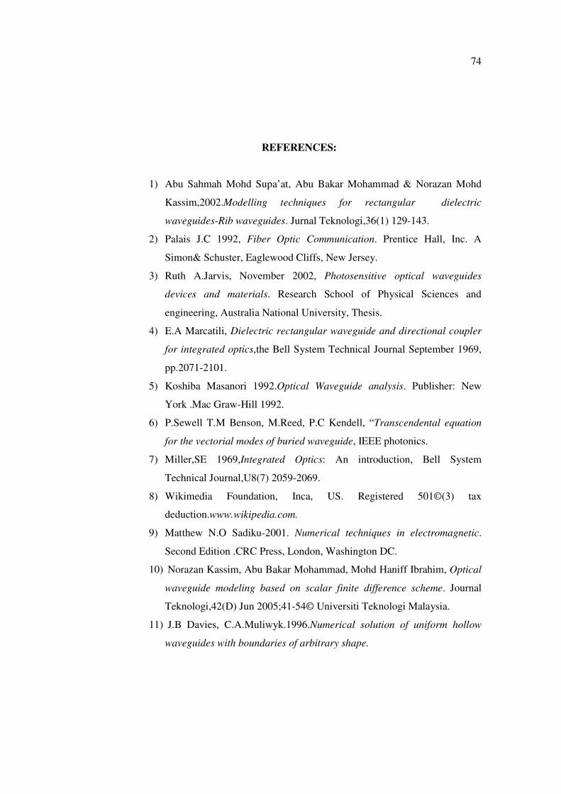
5.3 Effective index, neff and Normalized propagation constant, b analysis:
In order to determine the accuracy light intensity trapped inside the core area
within the structure, the effective index profile, neff should be in range between core
refractive index, ncore (n2) and cladding refractive index, n cladding (n1 and n3) ,
ncladding �neff �ncore. neff of the fundamental mode is related to the propagation constant
by 2
βλ
π. From the table 1(a) have 9 sample data neff that calculate from GUI which
from 3µm thickness to 7 µm thickness with rectangular channel. The range
neff,3.4281�neff�3.4294. From the data show that the neff in range between n core
and n cladding and it suitable with theory. The increasing of thickness will produce
the increasing of neff (figure 5.10 (a)). Therefore the value of � also increase and it
make the propagation light within the structure fully trapped into core active region
also propagation loss was decreased.
Due to difficulties in interpreting small differences of effective index values,
a more sensitive comparison is made by introducing a normalize propagation
constant,
2 2
2 2
eff substra te
guide substrate
n nb
n n
−=
−
The range of b from 3µm to 7 µm thicknesses was 0.3776 � b � 0.0241 as
shown at table 5.4. From the graph 5.10 (b), b was decreasing when thickness
increasing.
Table 5.4: 9 samples of data from GUI calculation (refer section 5.2)
t2(µm) 3 3.5 4 4.5 5
neff 3.4281 3.4314 3.4337 3.4357 3.4365
b 0.3776 0.2720 0.1994 0.1474 0.1089
t2(µm) 5.5 6 6.5 7
neff 3.4375 3.4382 3.4387 3.4392
b 0.0796 0.0568 0.0387 0.0241

67
0 1 2 3 4 5 6 73.428
3.43
3.432
3.434
3.436
3.438
3.44
3.442Effective Index (neff) Graph
Eff
ective I
ndex x
(neff
)
Thickness(um)
Figure 5.11 (a): Effective Index, neff graph
0 1 2 3 4 5 6 70
0.05
0.1
0.15
0.2
0.25
0.3
0.35
0.4Normalized propagation constant Graph
Norm
aliz
ed p
ropagation c
onsta
nt
Thickness(um)
Figure 5.11 (b): Normalized propagation constant, b graph

68
5.4 Comparison with previous analysis
The analysis of Buried rectangular waveguide is similar to that of the
dielectric guide in air. We study in this case the effect of anisotropy by considering a
buried guide of the same aspect ratio as the dielectric guide studied (t x w ,with w =
2t).From reference [14], the core has an anisotropic relative permittivity tensor with
components nx2=nz
2=2.31 and ny
2=2.19 and buried in a cladding of permittivity n2
2 =
2.05.
Figure 5.11 shows the dispersion characteristics for the lowest four modes of
propagation in the waveguide. Computed results agree very well with those obtained
by Ohtaka [15], Using a variational method and cylindrical harmonic function
expansions. His results have been used frequently as a standard for comparison.
Similarly to what was observed for the former example of a microwave dielectric
guide with isotropic core, the use of finite elements rather than simple truncation
greatly improves the accuracy of the solution in the low frequency range (kot <
3.5).The aspect ratio of the region divided into finite elements, the relative extent of
finite elements outside the core and indeed the mesh quadrilaterals.
Compare with this project result, although use difference refractive index as a
sample, but consider from effective index graph (see figure 5.10(a)) look neff
proportional with thickness. When thickness increase cause neff increase and it is
same with reference [14] and Ohtaka [15]. These project results are agreeable with
theory.

69
kot
Figure 5.12: Dispersion characteristic for the lowest four modes of an anisotropic
Rectangular dielectric waveguide

70
5.5 DISCUSSION
From the point of view of the electromagnetic analysis, Buried optical
waveguides can be characterized for not having closed boundaries, allowing the
fields to extend to infinity in the transverse direction. The wave guiding effect is not
produced by the presence of metallic walls but instead, being dielectric waveguides,
this is produced only by differences in the refractive index of materials involved.
Metal can be present, and indeed they are used in some optical guides, but their
behavior differs substantially to that observed at microwave frequencies where the
assumption of perfect conductivity is usually made. At optical wavelengths metals
show strong absorption, this can be represented by a complex permittivity or
refractive index. A dielectric material used in these guides often anisotropic and
some degree of absorption (loss) is common and unavoidable. Additionally, optical
waveguide frequently include active regions, effectively introducing a distributed
gain in the structure which can be represented in the same form as losses are treated,
that is, by a complex value of permittivity over those regions, this time with a
positive imaginary part. Also, leakage into the substrate is not uncommon. This can
occur in some optical wave guiding structures where the substrate or surrounding
material has a high refractive index. Leaky modes do not show an evanescent
behavior in the exterior region. They have complex propagation constants due to the
radiation loss and consequently they need a special treatment for their calculation.
Although increasing core thickness is another option theoretically, on a
practical level changing the core thickness is not desirable. A thick core has a lot of
side effects, such as higher thresholds for lasers, and introduces poorer saturation
characteristics for a semiconductor optical amplifier (SOA)[12].
The outputs for the simulation waveguide are influences by several factors
such as mesh size which mesh size are important factor in determine the accuracy of
the simulation process. Smaller mesh size will increase the accuracy of the Effective
Index and Normalized Propagation Constant. The mesh size also determine the
sharpness of the plotting either more accurate or not. But if the mesh size is too
small, the simulating will take a longer computational time. Another factor is

71
tolerance where tolerance input will determine the number of iteration that will be
process by the program. It is also contributing to the accuracy of the simulation
because the � used to calculate Effective Index and Normalized Propagation
Constant need to be converging. The smaller value of the tolerance will also increase
computational time. To determine the accuracy of this program, comparison was
made to other existing method. Results were compared to Finite Element Method.

CHAPTER 6
CONCLUSION AND RECOMMENDATION
6.1 Conclusion
A good design of the buried optical waveguide is intended to limit
propagation loss and the transition losses. So, in the integrated optical circuit, the
optimum design of the buried channel waveguide should support with low loss and
strongly optical confinement for practical implementation.
The propagation loss on straight waveguide dependence on the declaration
value of refractive index used between core and cladding waveguide. Besides that, it
wills dependence on value changers of lateral refractive index different whether it
can propagates in fully energy or not within the structure waveguide. Therefore, the
performance of buried waveguide will performed when refractive index different is
high. This lateral index different is produced by the dispersion of material refractive
indices and the electromagnetic different. So, the increased or refractive index
difference will produces strong an optical confinement. Besides that, core thickness
and core width influence the value of E-field, effective index and normalized
propagation constant. In conclusion, the simulation software in this project can helps
application of designed modeling performance especially aims for educational field
and industries. It also economical to user with cheaper price than available optical
software for example software from oversea that money exchange requirement.

73
6.2 Recommendation
There are two suitable recommendations to purpose in future works. In this
project, the implement of waveguide simulation was used in a symmetrical planar
waveguide. Firstly, I will recommend investigating an asymmetrical buried bend
waveguide as a medium used to further my simulation programmed. In order to
determine the accuracy of modeling techniques for calculating the result of integrated
optical waveguides, we should compare for other techniques such as Finite Element
Method (FEM) and Effective Index Method (EIM). The others software can be used
beside MATLAB, such as AUTO CAD and Beam Propagation Method (BPM) and
Bitline software, JAVA programming and Visual Basic programming.
74
REFERENCES:
1) Abu Sahmah Mohd Supa’at, Abu Bakar Mohammad & Norazan Mohd
Kassim,2002.Modelling techniques for rectangular dielectric
waveguides-Rib waveguides. Jurnal Teknologi,36(1) 129-143.
2) Palais J.C 1992, Fiber Optic Communication. Prentice Hall, Inc. A
Simon& Schuster, Eaglewood Cliffs, New Jersey.
3) Ruth A.Jarvis, November 2002, Photosensitive optical waveguides
devices and materials. Research School of Physical Sciences and
engineering, Australia National University, Thesis.
4) E.A Marcatili, Dielectric rectangular waveguide and directional coupler
for integrated optics,the Bell System Technical Journal September 1969,
pp.2071-2101.
5) Koshiba Masanori 1992.Optical Waveguide analysis. Publisher: New
York .Mac Graw-Hill 1992.
6) P.Sewell T.M Benson, M.Reed, P.C Kendell, “Transcendental equation
for the vectorial modes of buried waveguide, IEEE photonics.
7) Miller,SE 1969,Integrated Optics: An introduction, Bell System
Technical Journal,U8(7) 2059-2069.
8) Wikimedia Foundation, Inca, US. Registered 501©(3) tax
deduction.www.wikipedia.com.
9) Matthew N.O Sadiku-2001. Numerical techniques in electromagnetic.
Second Edition .CRC Press, London, Washington DC.
10) Norazan Kassim, Abu Bakar Mohammad, Mohd Haniff Ibrahim, Optical
waveguide modeling based on scalar finite difference scheme. Journal
Teknologi,42(D) Jun 2005;41-54© Universiti Teknologi Malaysia.
11) J.B Davies, C.A.Muliwyk.1996.Numerical solution of uniform hollow
waveguides with boundaries of arbitrary shape.

75
12) M.S Stern.1998.Semivectorial polarized finite difference method for
optical waveguides with arbitrary index profiles.IEEE Proc Vol.135, Pt
J.pp.56-63.
13) K.Bierwitrth, N.Schulz, F.arndt.1986.Finite difference analysis of
rectangular dielectric waveguide structure.IEEE Trans.Microwave
Theory Tech.Vol.34,P.P 1104-1114.
14) F. Anibal Fernandez, Yilong Lu.1996 Microwave and optical waveguide
analysis.Research studies press LTD, Somerset, England.
15) M. Ohtaka, Analysis of the guided modes in the anisotropic dielectric
rectangular waveguide, (in Japanese) Trans. Ins. Electron. Commun.
Eng.Japan, vol. J64-C, pp. 674-681, October 1981

APPENDIX A
Source Code for Buried waveguide modeling by
using MATLAB

77
function varargout = main page(varargin)
% main page M-file for main page.fig
% GUIJ, by itself, creates a new GUIJ or raises the existing
% singleton*.
%
% H = GUIJ returns the handle to a new GUIJ or the handle to
% the existing singleton*.
%
% GUIJ('CALLBACK',hObject,eventData,handles,...) calls the local
% function named CALLBACK in GUIJ.M with the given input arguments.
%
% GUIJ('Property','Value',...) creates a new GUIJ or raises the
% existing singleton*. Starting from the left, property value pairs
are
% applied to the GUI before guij_OpeningFunction gets called. An
% unrecognized property name or invalid value makes property
application
% stop. All inputs are passed to guij_OpeningFcn via varargin.
%
% *See GUI Options on GUIDE's Tools menu. Choose "GUI allows only one
% instance to run (singleton)".
%
% See also: GUIDE, GUIDATA, GUIHANDLES
% Edit the above text to modify the response to help guij
% Last Modified by GUIDE v2.5 18-Mar-2008 00:07:44
% Begin initialization code - DO NOT EDIT
gui_Singleton = 1;
gui_State = struct('gui_Name', mfilename, ...
'gui_Singleton', gui_Singleton, ...
'gui_OpeningFcn', @guij_OpeningFcn, ...
'gui_OutputFcn', @guij_OutputFcn, ...
'gui_LayoutFcn', [] , ...
'gui_Callback', []);
if nargin && ischar(varargin{1})
gui_State.gui_Callback = str2func(varargin{1});
end
if nargout
[varargout{1:nargout}] = gui_mainfcn(gui_State, varargin{:});
else
gui_mainfcn(gui_State, varargin{:});
end
% End initialization code - DO NOT EDIT
% --- Executes just before guij is made visible.
function guij_OpeningFcn(hObject, eventdata, handles, varargin)
% This function has no output args, see OutputFcn.
% hObject handle to figure
% eventdata reserved - to be defined in a future version of MATLAB
% handles structure with handles and user data (see GUIDATA)
% varargin command line arguments to guij (see VARARGIN)
% Choose default command line output for guij
handles.output = hObject;
[x,map]=imread('officialutmslide.jpg');
image(x)
colormap(map)
axis off
% Update handles structure
guidata(hObject, handles);
% UIWAIT makes main page wait for user response (see UIRESUME)
% uiwait(handles.figure1);

78
% --- Outputs from this function are returned to the command line.
function varargout = main page_OutputFcn(hObject, eventdata, handles)
% varargout cell array for returning output args (see VARARGOUT);
% hObject handle to figure
% eventdata reserved - to be defined in a future version of MATLAB
% handles structure with handles and user data (see GUIDATA)
% Get default command line output from handles structure
varargout{1} = handles.output;
% --- Executes on button press in pushbutton1.
function pushbutton1_Callback(hObject, eventdata, handles)
% hObject handle to pushbutton1 (see GCBO)
% eventdata reserved - to be defined in a future version of MATLAB
% handles structure with handles and user data (see GUIDATA)
[pushbutton1]=wg3x3();
% --- Executes on button press in pushbutton2.
function pushbutton2_Callback(hObject, eventdata, handles)
% hObject handle to pushbutton2 (see GCBO)
% eventdata reserved - to be defined in a future version of MATLAB
% handles structure with handles and user data (see GUIDATA)
[pushbutton2]=wg5x5();
% --- Executes on button press in pushbutton3.
function pushbutton3_Callback(hObject, eventdata, handles)
% hObject handle to pushbutton3 (see GCBO)
% eventdata reserved - to be defined in a future version of MATLAB
% handles structure with handles and user data (see GUIDATA)
[pushbutton3]=wg7x7();
% --- Executes on button press in pushbutton4.
function pushbutton4_Callback(hObject, eventdata, handles)
% hObject handle to pushbutton4 (see GCBO)
% eventdata reserved - to be defined in a future version of MATLAB
% handles structure with handles and user data (see GUIDATA)
[pushbutton4]=CALCULATION();
% --- Executes on selection change in popupmenu1.
function popupmenu1_Callback(hObject, eventdata, handles)
% hObject handle to popupmenu1 (see GCBO)
% eventdata reserved - to be defined in a future version of MATLAB
% handles structure with handles and user data (see GUIDATA)
% Hints: contents = get(hObject,'String') returns popupmenu1 contents as
cell array
% contents{get(hObject,'Value')} returns selected item from
popupmenu1
% --- Executes during object creation, after setting all properties.
function popupmenu1_CreateFcn(hObject, eventdata, handles)
% hObject handle to popupmenu1 (see GCBO)
% eventdata reserved - to be defined in a future version of MATLAB
% handles empty - handles not created until after all CreateFcns called
% Hint: popupmenu controls usually have a white background on Windows.
% See ISPC and COMPUTER.
if ispc && isequal(get(hObject,'BackgroundColor'),
get(0,'defaultUicontrolBackgroundColor'))
set(hObject,'BackgroundColor','white');
end
% --- Executes on selection change in popupmenu3.
function popupmenu3_Callback(hObject, eventdata, handles)
% hObject handle to popupmenu3 (see GCBO)
% eventdata reserved - to be defined in a future version of MATLAB
79
% handles structure with handles and user data (see GUIDATA)
% Hints: contents = get(hObject,'String') returns popupmenu3 contents as
cell array
% contents{get(hObject,'Value')} returns selected item from
popupmenu3
% --- Executes during object creation, after setting all properties.
function popupmenu3_CreateFcn(hObject, eventdata, handles)
% hObject handle to popupmenu3 (see GCBO)
% eventdata reserved - to be defined in a future version of MATLAB
% handles empty - handles not created until after all CreateFcns called
% Hint: popupmenu controls usually have a white background on Windows.
% See ISPC and COMPUTER.
if ispc && isequal(get(hObject,'BackgroundColor'),
get(0,'defaultUicontrolBackgroundColor'))
set(hObject,'BackgroundColor','white');
end
function edit1_Callback(hObject, eventdata, handles)
% hObject handle to edit1 (see GCBO)
% eventdata reserved - to be defined in a future version of MATLAB
% handles structure with handles and user data (see GUIDATA)
% Hints: get(hObject,'String') returns contents of edit1 as text
% str2double(get(hObject,'String')) returns contents of edit1 as a
double
% --- Executes during object creation, after setting all properties.
function edit1_CreateFcn(hObject, eventdata, handles)
% hObject handle to edit1 (see GCBO)
% eventdata reserved - to be defined in a future version of MATLAB
% handles empty - handles not created until after all CreateFcns called
% Hint: edit controls usually have a white background on Windows.
% See ISPC and COMPUTER.
if ispc && isequal(get(hObject,'BackgroundColor'),
get(0,'defaultUicontrolBackgroundColor'))
set(hObject,'BackgroundColor','white');
end
% --- Executes on selection change in popupmenu4.
function popupmenu4_Callback(hObject, eventdata, handles)
% hObject handle to popupmenu4 (see GCBO)
% eventdata reserved - to be defined in a future version of MATLAB
% handles structure with handles and user data (see GUIDATA)
% Hints: contents = get(hObject,'String') returns popupmenu4 contents as
cell array
% contents{get(hObject,'Value')} returns selected item from
popupmenu4
% --- Executes during object creation, after setting all properties.
function popupmenu4_CreateFcn(hObject, eventdata, handles)
% hObject handle to popupmenu4 (see GCBO)
% eventdata reserved - to be defined in a future version of MATLAB
% handles empty - handles not created until after all CreateFcns called
% Hint: popupmenu controls usually have a white background on Windows.
% See ISPC and COMPUTER.
if ispc && isequal(get(hObject,'BackgroundColor'),
get(0,'defaultUicontrolBackgroundColor'))

80
set(hObject,'BackgroundColor','white');
end
% --- Executes on button press in pushbutton5.
function pushbutton5_Callback(hObject, eventdata, handles)
% hObject handle to pushbutton5 (see GCBO)
% eventdata reserved - to be defined in a future version of MATLAB
% handles structure with handles and user data (see GUIDATA)
[pushbutton5]=aplication()
% --- Executes on button press in pushbutton6.
function pushbutton6_Callback(hObject, eventdata, handles)
% hObject handle to pushbutton6 (see GCBO)
% eventdata reserved - to be defined in a future version of MATLAB
% handles structure with handles and user data (see GUIDATA)
[pushbutton6]=ANALYSIS2()
CALCULATION PART
function varargout = CALCULATION(varargin)
% CALCULATION M-file for CALCULATION.fig
% CALCULATION, by itself, creates a new CALCULATION or raises the
existing
% singleton*.
%
% H = CALCULATION returns the handle to a new CALCULATION or the handle
to
% the existing singleton*.
%
% CALCULATION('CALLBACK',hObject,eventData,handles,...) calls the local
% function named CALLBACK in CALCULATION.M with the given input
arguments.
%
% CALCULATION('Property','Value',...) creates a new CALCULATION or
raises the
% existing singleton*. Starting from the left, property value pairs
are
% applied to the GUI before CALCULATION_OpeningFunction gets called.
An
% unrecognized property name or invalid value makes property
application
% stop. All inputs are passed to CALCULATION_OpeningFcn via varargin.
%
% *See GUI Options on GUIDE's Tools menu. Choose "GUI allows only one
% instance to run (singleton)".
%
% See also: GUIDE, GUIDATA, GUIHANDLES
% Copyright 2002-2003 The MathWorks, Inc.
% Edit the above text to modify the response to help CALCULATION
% Last Modified by GUIDE v2.5 06-Apr-2008 15:02:22
% Begin initialization code - DO NOT EDIT
gui_Singleton = 1;
gui_State = struct('gui_Name', mfilename, ...
'gui_Singleton', gui_Singleton, ...
'gui_OpeningFcn', @CALCULATION_OpeningFcn, ...
'gui_OutputFcn', @CALCULATION_OutputFcn, ...
'gui_LayoutFcn', [] , ...
'gui_Callback', []);
if nargin && ischar(varargin{1})
gui_State.gui_Callback = str2func(varargin{1});
end
81
if nargout
[varargout{1:nargout}] = gui_mainfcn(gui_State, varargin{:});
else
gui_mainfcn(gui_State, varargin{:});
end
% End initialization code - DO NOT EDIT
% --- Executes just before CALCULATION is made visible.
function CALCULATION_OpeningFcn(hObject, eventdata, handles, varargin)
% This function has no output args, see OutputFcn.
% hObject handle to figure
% eventdata reserved - to be defined in a future version of MATLAB
% handles structure with handles and user data (see GUIDATA)
% varargin command line arguments to CALCULATION (see VARARGIN)
% Choose default command line output for CALCULATION
handles.output = hObject;
% Update handles structure
guidata(hObject, handles);
[x,map]=imread('structure.JPG');
image(x)
colormap(map)
axis off
% Update handles structure
guidata(hObject, handles);
% UIWAIT makes CALCULATION wait for user response (see UIRESUME)
% uiwait(handles.figure1);
% --- Outputs from this function are returned to the command line.
function varargout = CALCULATION_OutputFcn(hObject, eventdata, handles)
% varargout cell array for returning output args (see VARARGOUT);
% hObject handle to figure
% eventdata reserved - to be defined in a future version of MATLAB
% handles structure with handles and user data (see GUIDATA)
% Get default command line output from handles structure
varargout{1} = handles.output;
function t2_Callback(hObject, eventdata, handles)
% hObject handle to t2 (see GCBO)
% eventdata reserved - to be defined in a future version of MATLAB
% handles structure with handles and user data (see GUIDATA)
% Hints: get(hObject,'String') returns contents of t2 as text
% str2double(get(hObject,'String')) returns contents of t2 as a
double
t2= str2double(get(hObject, 'String'));
if isnan(t2)
set(hObject, 'String', 0);
errordlg('Input must be a number','Error');
end
% Save the new volume value
handles.metricdata.t2=t2;
guidata(hObject,handles)
% --- Executes during object creation, after setting all properties.
function t2_CreateFcn(hObject, eventdata, handles)
% hObject handle to t2 (see GCBO)
% eventdata reserved - to be defined in a future version of MATLAB

82
% handles empty - handles not created until after all CreateFcns called
% Hint: edit controls usually have a white background on Windows.
% See ISPC and COMPUTER.
if ispc && isequal(get(hObject,'BackgroundColor'),
get(0,'defaultUicontrolBackgroundColor'))
set(hObject,'BackgroundColor','white');
end
function W_Callback(hObject, eventdata, handles)
% hObject handle to W (see GCBO)
% eventdata reserved - to be defined in a future version of MATLAB
% handles structure with handles and user data (see GUIDATA)
% Hints: get(hObject,'String') returns contents of W as text
% str2double(get(hObject,'String')) returns contents of W as a double
W= str2double(get(hObject, 'String'));
if isnan(W)
set(hObject, 'String', 0);
errordlg('Input must be a number','Error');
end
% Save the new volume value
handles.metricdata.W=W;
guidata(hObject,handles)
% --- Executes during object creation, after setting all properties.
function W_CreateFcn(hObject, eventdata, handles)
% hObject handle to W (see GCBO)
% eventdata reserved - to be defined in a future version of MATLAB
% handles empty - handles not created until after all CreateFcns called
% Hint: edit controls usually have a white background on Windows.
% See ISPC and COMPUTER.
if ispc && isequal(get(hObject,'BackgroundColor'),
get(0,'defaultUicontrolBackgroundColor'))
set(hObject,'BackgroundColor','white');
end
function n1_Callback(hObject, eventdata, handles)
% hObject handle to n1 (see GCBO)
% eventdata reserved - to be defined in a future version of MATLAB
% handles structure with handles and user data (see GUIDATA)
% Hints: get(hObject,'String') returns contents of n1 as text
% str2double(get(hObject,'String')) returns contents of n1 as a
double
n1= str2double(get(hObject, 'String'));
if isnan(n1)
set(hObject, 'String', 0);
errordlg('Input must be a number','Error');
end
% Save the new volume value
handles.metricdata.n1=n1;
guidata(hObject,handles)
% --- Executes during object creation, after setting all properties.
function n1_CreateFcn(hObject, eventdata, handles)
% hObject handle to n1 (see GCBO)
% eventdata reserved - to be defined in a future version of MATLAB
% handles empty - handles not created until after all CreateFcns called
83
% Hint: edit controls usually have a white background on Windows.
% See ISPC and COMPUTER.
if ispc && isequal(get(hObject,'BackgroundColor'),
get(0,'defaultUicontrolBackgroundColor'))
set(hObject,'BackgroundColor','white');
end
function n2_Callback(hObject, eventdata, handles)
% hObject handle to n2 (see GCBO)
% eventdata reserved - to be defined in a future version of MATLAB
% handles structure with handles and user data (see GUIDATA)
% Hints: get(hObject,'String') returns contents of n2 as text
% str2double(get(hObject,'String')) returns contents of n2 as a
double
n2= str2double(get(hObject, 'String'));
if isnan(n2)
set(hObject, 'String', 0);
errordlg('Input must be a number','Error');
end
% Save the new volume value
handles.metricdata.n2=n2;
guidata(hObject,handles)
% --- Executes during object creation, after setting all properties.
function n2_CreateFcn(hObject, eventdata, handles)
% hObject handle to n2 (see GCBO)
% eventdata reserved - to be defined in a future version of MATLAB
% handles empty - handles not created until after all CreateFcns called
% Hint: edit controls usually have a white background on Windows.
% See ISPC and COMPUTER.
if ispc && isequal(get(hObject,'BackgroundColor'),
get(0,'defaultUicontrolBackgroundColor'))
set(hObject,'BackgroundColor','white');
end
function n3_Callback(hObject, eventdata, handles)
% hObject handle to n3 (see GCBO)
% eventdata reserved - to be defined in a future version of MATLAB
% handles structure with handles and user data (see GUIDATA)
% Hints: get(hObject,'String') returns contents of n3 as text
% str2double(get(hObject,'String')) returns contents of n3 as a
double
n3= str2double(get(hObject, 'String'));
if isnan(n3)
set(hObject, 'String', 0);
errordlg('Input must be a number','Error');
end
% Save the new volume value
handles.metricdata.n3=n3;
guidata(hObject,handles)
% --- Executes during object creation, after setting all properties.
function n3_CreateFcn(hObject, eventdata, handles)
% hObject handle to n3 (see GCBO)
% eventdata reserved - to be defined in a future version of MATLAB
% handles empty - handles not created until after all CreateFcns called
% Hint: edit controls usually have a white background on Windows.
% See ISPC and COMPUTER.
if ispc && isequal(get(hObject,'BackgroundColor'),
get(0,'defaultUicontrolBackgroundColor'))

84
set(hObject,'BackgroundColor','white');
end
% --- Executes on button press in CALCULATE.
function CALCULATE_Callback(hObject, eventdata, handles)
% hObject handle to CALCULATE (see GCBO)
% eventdata reserved - to be defined in a future version of MATLAB
% handles structure with handles and user data (see GUIDATA)
dx1=0.1; %handles.metricdata.dx;
dy1=0.1; %handles.metricdata.dy;
t2=handles.metricdata.t2;
t3=2; %handles.metricdata.t3;
w=handles.metricdata.W;
h=2;%handles.metricdata.h;
lamda=1.55; %handles.metricdata.lamda;
a=10;%handles.metricdata.a;
n1=handles.metricdata.n1;
n2=handles.metricdata.n2;
n3=handles.metricdata.n3;
Iteration1=500; %handles.metricdata.Iteration;
lamda=lamda*10^(-6);
miu=4*pi*10^(-7);
heks=8.854*10^(-12);
C=3*10^8;
kiraan=1;
T=h+t2+t3;
L=a+a+w;
mT=round(T/dy1);
mh=round(h/dy1);
mt2=round(t2/dy1);
mt3=round(t3/dy1);
mL=round(L/dx1);
mw=round(w/dx1);
ma=round(a/dx1);
r=sqrt((dy1^2)/(dx1^2));
N=ones((mT+1),(mL+1));
%*****************************************
%Buried Optical waveguide modeling
%*****************************************
for i=(mT+1):-1:(mh+mt2+2)
for j=1:1:(mL+1)
N(i,j)=n4;
end
end
for i=(mh+mt2+1):-1:(mh+2)
for j=(ma+1):1:(ma+mw+2)
N(i,j)=n2;
end
end
for i=(mh+mt2+1):-1:(mh+2)
for j=1:1:ma
N(i,j)=n3;
end
end
for i=(mh+mt2+1):-1:(mh+2)
for j=(ma+mw+1):1:(mL+1)
N(i,j)=n3;
end

85
end
for i=mh:-1:1
for j=1:1:(mL+1)
N(i,j)=n1;
end
end
f=C/lamda;
omega=2*pi*f;
ko=sqrt((omega^2)*miu*heks);
beta=ko*n4;
ddx=dx1*10^(-6);
E=ones((mT+1),(mL+1));
E(:,1)=0;
E(:,(mL+1))=0;
E(1,:)=0;
E((mT+1),:)=0;
%******************************************
%calculation start
%*****************************************
while kiraan<Iteration1
for i=mT:-1:2
for j=2:1:mL
E(i,j)=(E((i+1),j) + E((i-1),j) + (E(i,(j+1)) + E(i,(j-
1)))*r^2)/(2*(1+r^2) - (ddx^2)*((ko^2)*(N(i,j)^2)-beta^2));
end
end
kiraan = kiraan + 1;
ddy=dy1*10^(-6);
%******************************************
% neff calculation
%******************************************
%Calculate num and den for Raleigh Equation
num=0; den=0;
for i=mT:-1:2
for j=2:1:mL
d2Ex=(E((i+1),j)+E((i-1),j)-2*E(i,j))/(ddx*ddx);
d2Ey=(E(i,(j+1))+E(i,(j-1))-2*E(i,j))/(ddy*ddy);
num=num+dy1*dx1*(E(i,j)*(d2Ex+d2Ey+E(i,j)*N(i,j)*N(i,j)*ko*ko));
den=den+dy1*dx1*E(i,j)*E(i,j);
%calculate new beta
beta=sqrt(num/den);
%effective index calculation
Neff=beta*lamda/(2*pi);
%normalized calculation constant calculation
b=((Neff*Neff-n2*n2)/(n3*n3-n2*n2))*pi;
end
end
%normalization equation
Etotal=0;
for j=1:1:mL
for i=1:1:mT
Etotal=Etotal + E(i,j);% Larger value E(i,j)
end
end
for j=1:1:mL
for i=1:1:mT
E(i,j)=E(i,j)/Etotal;% normalize equation

86
end
end
end
set(handles.Neff,'String',Neff);
set(handles.b,'String', b);
x=0:dx1:L;
y=T:-dy1:0;
figure
subplot(2,2,2);
mesh(x,y,E)
xlabel('X-axis,mikrometer')
ylabel('Y-axis,mikrometer')
zlabel('E distribution')
title('E-field Profile')
subplot(2,2,1);
mesh(x,y,N)
title('Refractive Index Profile')
subplot(2,2,3);
contour(x,y,E)
xlabel('Waveguide width (um)')
ylabel('Waveguide heigth (um)')
title('E-field Contour Plot')
hold on
x=[0 L L 0 0];
y=[0 0 T T 0];
line(x,y,'linewidth',1);
hold on
x=[0 L];
y=[t3 t3];
line(x,y,'linewidth',1);
hold on
x=[0 a a a+w a+w L];
y=[t2+h t2+h t3 t3 t2+h t2+h];
line(x,y,'linewidth',1);
hold on
% --- Executes on button press in MENU.
function MENU_Callback(hObject, eventdata, handles)
% hObject handle to MENU (see GCBO)
% eventdata reserved - to be defined in a future version of MATLAB
% handles structure with handles and user data (see GUIDATA)
[MENU]=main page();
main
function edit11_Callback(hObject, eventdata, handles)
% hObject handle to edit11 (see GCBO)
% eventdata reserved - to be defined in a future version of MATLAB
% handles structure with handles and user data (see GUIDATA)
% Hints: get(hObject,'String') returns contents of edit11 as text
% str2double(get(hObject,'String')) returns contents of edit11 as a
double
% --- Executes during object creation, after setting all properties.
function edit11_CreateFcn(hObject, eventdata, handles)
% hObject handle to edit11 (see GCBO)
% eventdata reserved - to be defined in a future version of MATLAB
% handles empty - handles not created until after all CreateFcns called

87
% Hint: edit controls usually have a white background on Windows.
% See ISPC and COMPUTER.
if ispc && isequal(get(hObject,'BackgroundColor'),
get(0,'defaultUicontrolBackgroundColor'))
set(hObject,'BackgroundColor','white');
end