12.docx · web viewm * m could be greater than 1 or smaller than 1 let’s derive m* the group...
TRANSCRIPT
Lecture 12: Continue the Band Theory of SolidsBand Structures
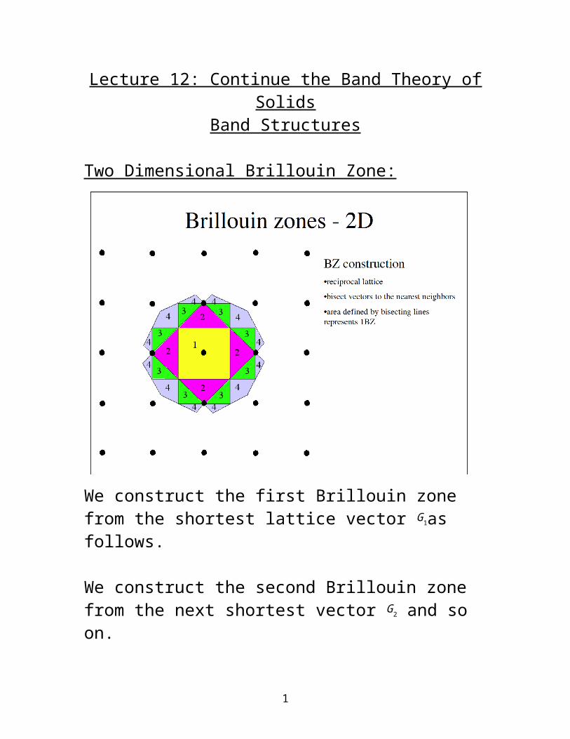
Two Dimensional Brillouin Zone:
We construct the first Brillouin zone from the shortest lattice vector G1as follows.
We construct the second Brillouin zone from the next shortest vector G2 and so on.
Brillouin Zones- 2D
1
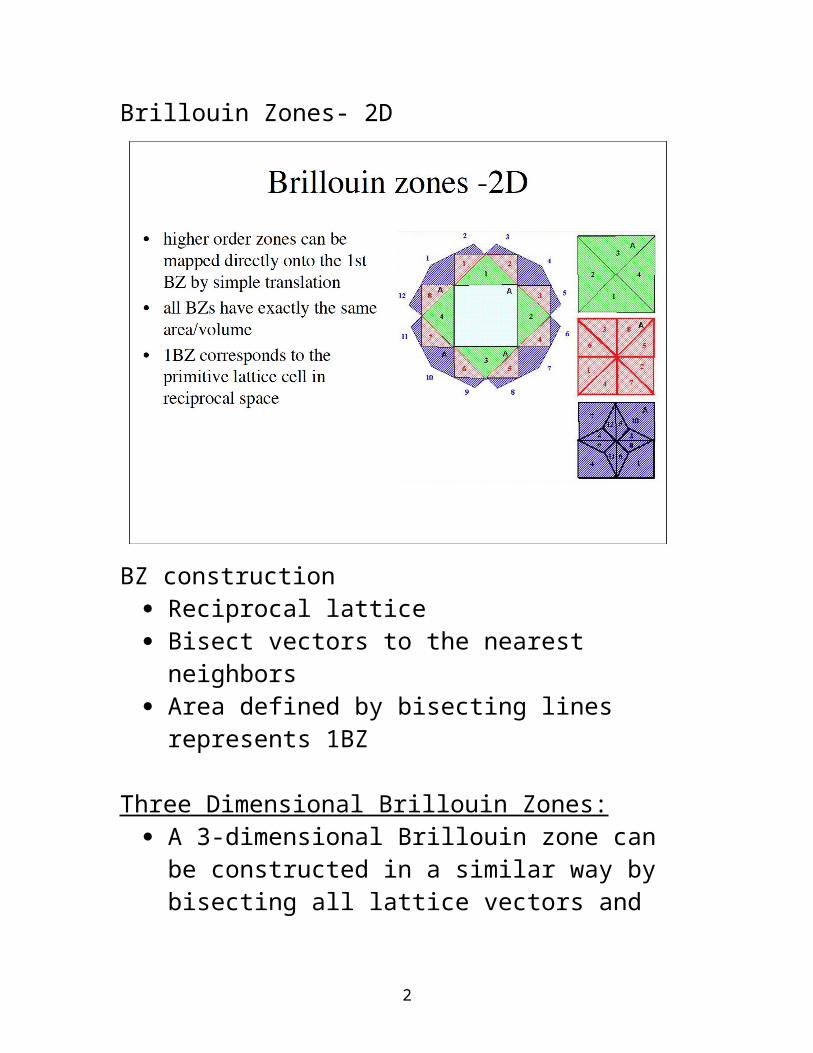
BZ construction Reciprocal lattice Bisect vectors to the nearest neighbors Area defined by bisecting lines represents 1BZ
Three Dimensional Brillouin Zones: A 3-dimensional Brillouin zone can be constructed
in a similar way by bisecting all lattice vectors and placing planes perpendicular to these points of bisection.
This is similar to the Wigner Seitz cell in the real lattice.
Wigner Seitz Cell:
2
A primitive unit cell which shows the cubic symmetry of the lattice( for the cubic system).(real lattice)
The First Brillouin zone is the Wigner Seitz cell in the reciprocal lattice
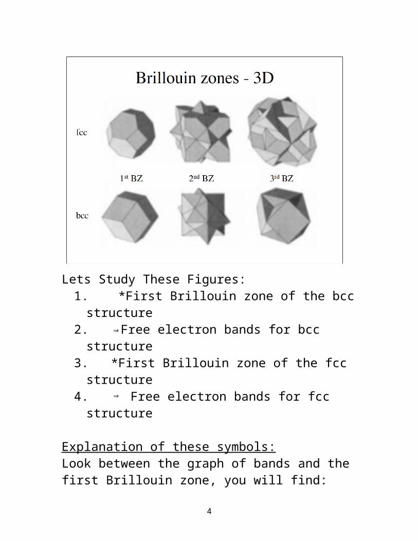
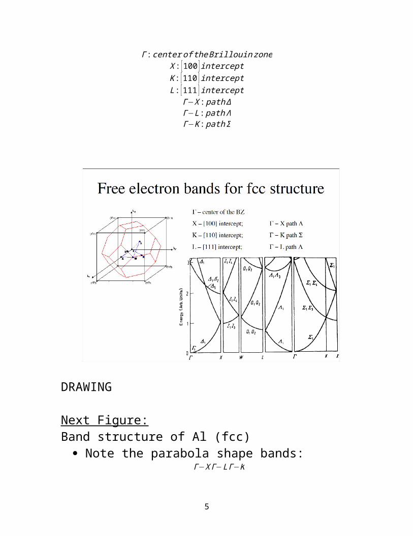
Lets Study These Figures:1. *First Brillouin zone of the bcc structure2. ⇒Free electron bands for bcc structure3. *First Brillouin zone of the fcc structure4. ⇒ Free electron bands for fcc structure
Explanation of these symbols:Look between the graph of bands and the first Brillouin zone, you will find:
Γ :center of the Brillouin zoneΧ : [100 ] intercept
3
Κ : [110 ] interceptL : [111 ] interceptΓ−Χ : path ΔΓ−L: path ΛΓ−Κ : path Σ
DRAWING
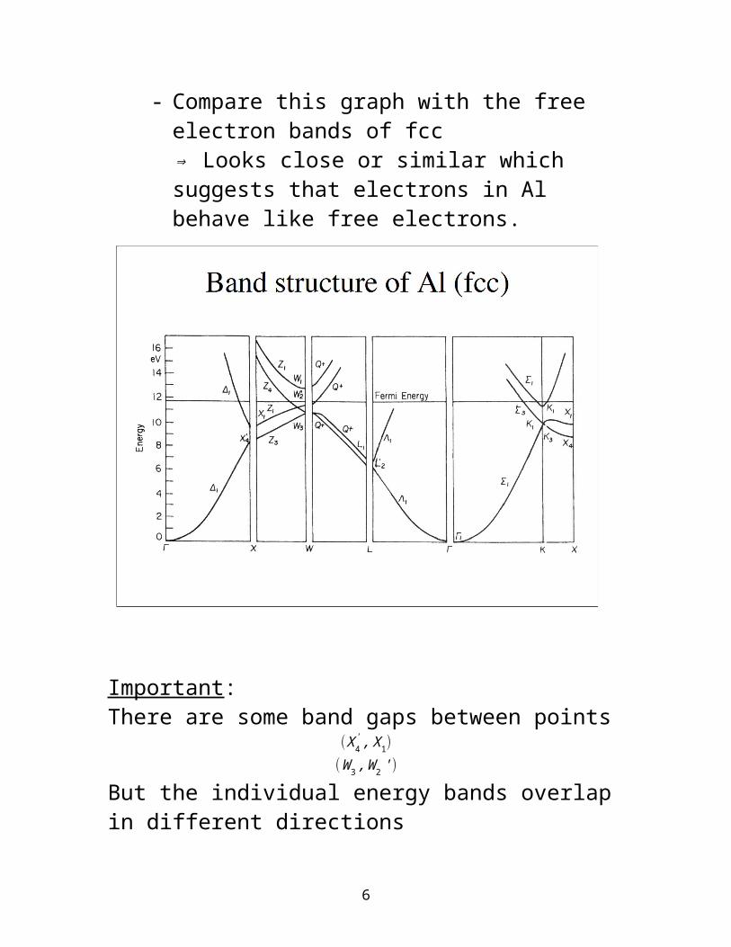
Next Figure:Band structure of Al (fcc)
Note the parabola shape bands:Γ−Χ Γ−L Γ−Κ
- Compare this graph with the free electron bands of fcc⇒ Looks close or similar which suggests that electrons in Al behave like free electrons.
4
Important:There are some band gaps between points
(X 4' , X1)
(W 3 ,W 2 ' )
But the individual energy bands overlap in different directions
⇒No band gap exists as a whole
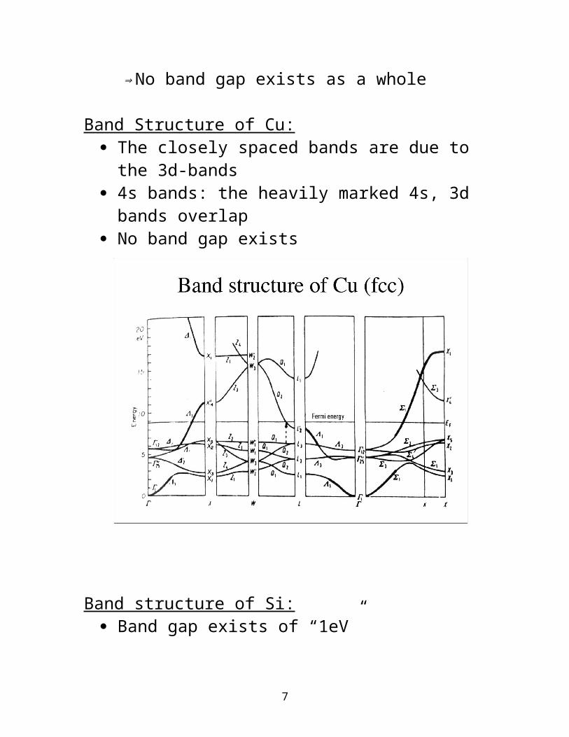
Band Structure of Cu: The closely spaced bands are due to the 3d-bands 4s bands: the heavily marked 4s, 3d bands overlap No band gap exists
5
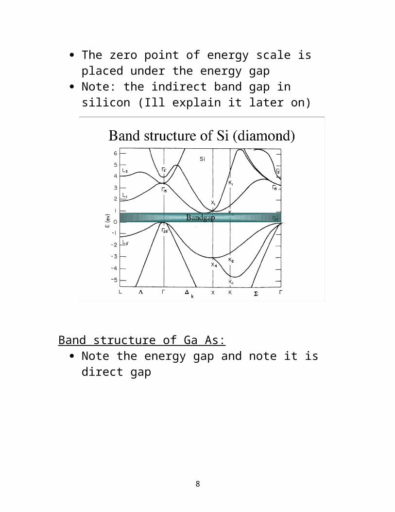
Band structure of Si: Band gap exists of “1eV” The zero point of energy scale is placed under the
energy gap Note: the indirect band gap in silicon (Ill explain it
later on)
6
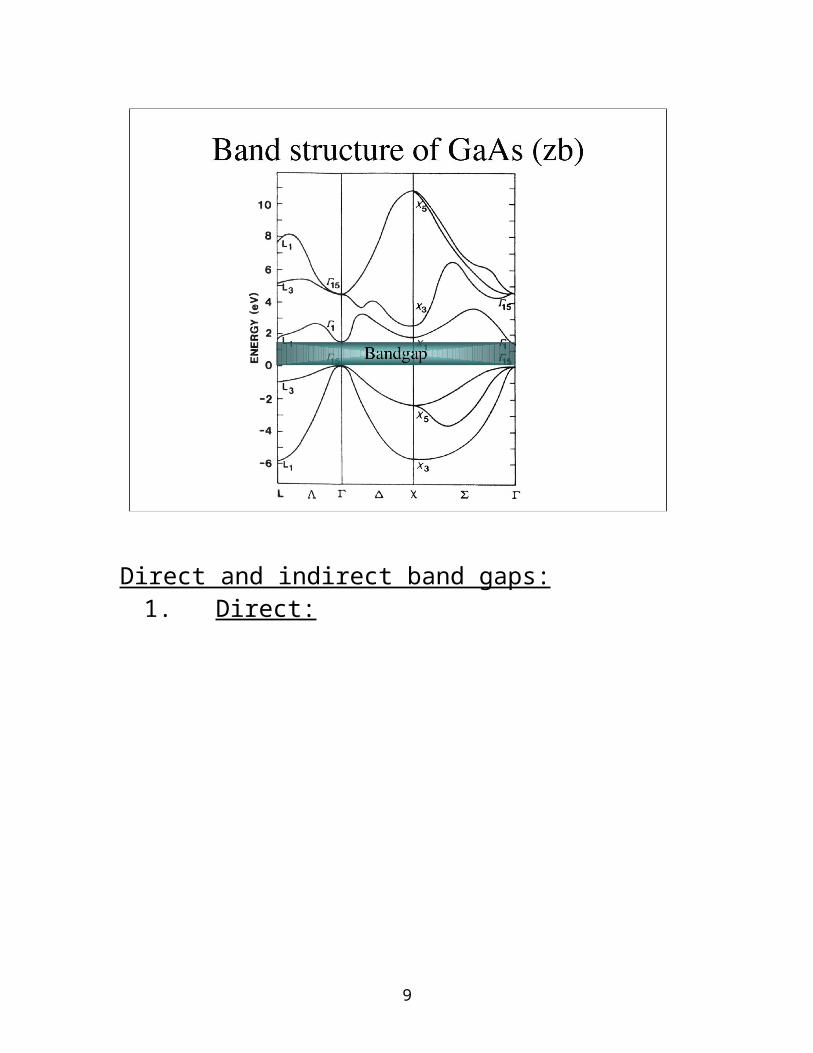
Band structure of Ga As: Note the energy gap and note it is direct gap
7
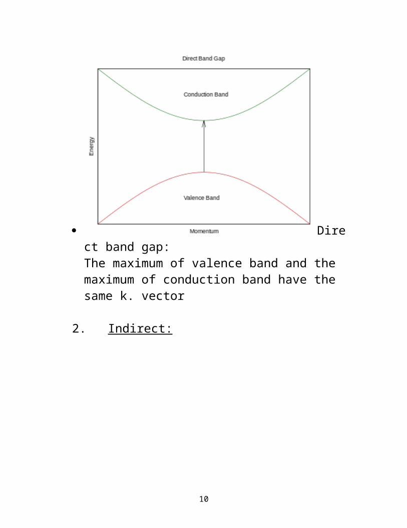
Direct and indirect band gaps:1. Direct:
8
Direct band gap: The maximum of valence band and the maximum of conduction band have the same k. vector
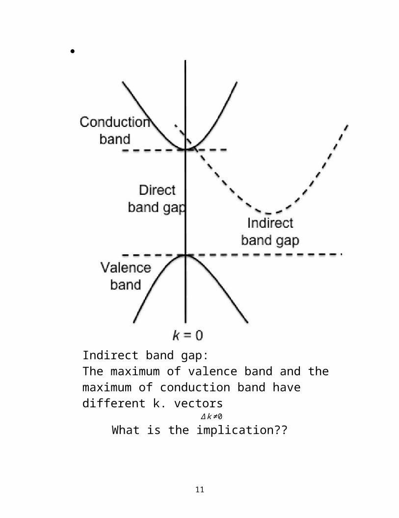
2. Indirect:
9
Indirect band gap:The maximum of valence band and the maximum of conduction band have different k. vectors
Δ k≠0
What is the implication??
We still need to understand more about the shape of band structure.To do that, we need to understand the effective mass:
10
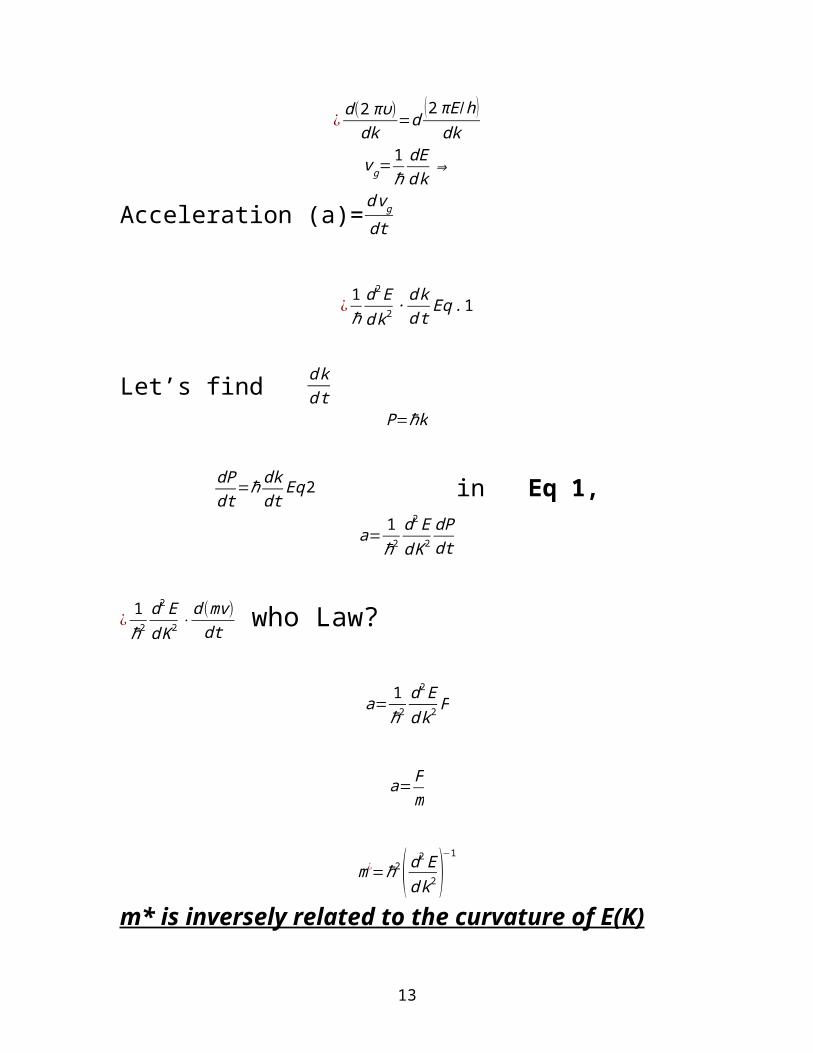
Effective mass of electron: m*
The mass of an electron in a solid is deviated from the free electron mass due to interactions of electron- electron, and electrons-ions.
m¿
m could be greater than 1 or smaller than 1
Let’s derive m*
The group velocity vg : vg=
dωdk
ω=2πυ k=2πλ
¿d (2πυ)dk
=d (2πE /h )dk
vg=1ℏ
dEd k
⇒
Acceleration (a)=d vg
dt
¿ 1ℏd2Ed k2
∙ d kd t
Eq .1
Let’s find d kd tP= kℏ
11
dPdt
=ℏ dkdt
Eq2 in Eq 1,
a= 1ℏ2
d2Ed Κ2
dPdt
¿ 1ℏ2
d2Ed Κ2 ⋅
d (mv )dt who Law?
a= 1ℏ2
d2Ed k2
F
a= Fm
m¿=ℏ2( d2Ed k2 )−1
m* is inversely related to the curvature of E(K)
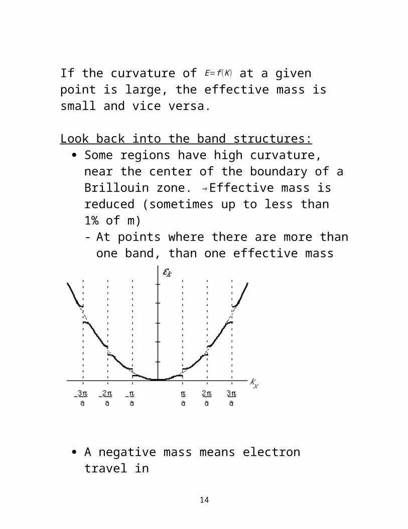
If the curvature of E=f (K) at a given point is large, the effective mass is small and vice versa.
Look back into the band structures: Some regions have high curvature, near the center
of the boundary of a Brillouin zone. ⇒Effective mass is reduced (sometimes up to less than 1% of m)- At points where there are more than one band,
than one effective mass
12
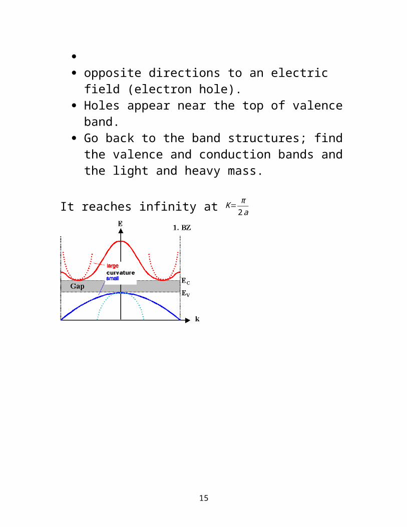
A negative mass means electron travel in opposite directions to an electric field (electron
hole). Holes appear near the top of valence band. Go back to the band structures; find the valence
and conduction bands and the light and heavy mass.
It reaches infinity at K= π2a
13
14
15