13 next generation technologies - introduction
TRANSCRIPT
INTRODUCTION
Information processing is used directly in computer products and indirectly as the brains in
Òsmart productsÓ such as electronic date books, central office telephone switches, medical moni-
toring instruments, and the latest luxury cars.
The incredible thirst we have for information processing power is fueling the migration of yester-
dayÕs super computer abilities into tomorrowÕs shirt pocket. Ever more versatile electronics-based
products are creating a transformation in our lives and culture.
For example:
¥ The pocket calculator has single-handedly eliminated the slide rule and the desktop calculator.
¥ The introduction of electronic word processing has virtually eliminated the electric type-
writer, which eliminated the manual typewriter.
¥ The CD player, based on laser diodes, high-resolution analog-to-digital converters, digital
signal processors, and microprocessors, has virtually eliminated the production and sale of
vinyl records (current revival here).
¥ Microprocessors have filtered so far into cars that electronics training is essential for car
mechanics.
¥ Personal electronic information managers, such as the ÒBossÓ and the ÒWizard,Ó are quickly
causing the daytimer pocket calendar to disappear.
¥ Cellular phone architecture, support electronics networks, and small, portable phones are
changing our travel habits and ability to stay in touch.
¥ The introduction of the FAX machine has nearly eliminated courier service companies.
¥ The microcomputer and laser printer created the desktop publishing industry and put the
power of the press in the hands of the individual.
¥ The office copier eliminated the carbon copy and transformed the reproduction and dissem-
ination of information.
¥ A second-generation revolution will reduce the volume of printed paper in favor of elec-
tronically transmitted, stored, and displayed information, possibly replacing books, maga-
zines, and newspapers.
INTEGRATED CIRCUIT ENGINEERING CORPORATION 13-1
13 NEXT GENERATION TECHNOLOGIES

¥ Personal computers revolutionized word processing, database management, and video and
graphical presentation.
¥ Computer-aided design and simulation is replacing hand-drawn blueprints and three-
dimentional models.
¥ SMART cards are allowing 24-hour access to personal information (accounts, medical
records, etc.)
¥ Digital cameras and imaging are allowing instant video imaging, photo-enhancement, and
previewing.
¥ The proliferation of the handheld video camera has made possible the ability to record spon-
taneous crimes and unique events, later showing these films to an audience of millions in
some cases.
¥ The prevalence of faxes and e-mail has toppled governments because proliferation of infor-
mation by individuals cannot be suppressed.
¥ The Information Superhighway has placed the resources of every great library in the world,
in the hands of any individual, anywhere.
¥ The Web is also an enabler for personal investment as access previously available only to large
companies and investment firms is now available to any individual with a PC and modem.
It is these products and others like them that ultimately are fueling the advance of IC technology
by setting our expectations higher and higher, which in turn drives the advancement of packag-
ing technology.
It is a given that IC devices will continue their steady advances of:
¥ Smaller features
¥ Shorter intrinsic gate delays
¥ Larger die size
¥ More functions per chip
¥ More power generated
¥ Higher bandwidth signals
¥ Lower cost per function
There will be a few IC advances that will relieve some of the increased packaging burden, such as:
¥ Lower rail voltages for CMOS devices yielding lower power dissipation.
¥ Massively parallel architectures that, at some integration level, will use an interconnect net-
work closer to a bussed architecture than a random architecture, requiring less interconnect
density.
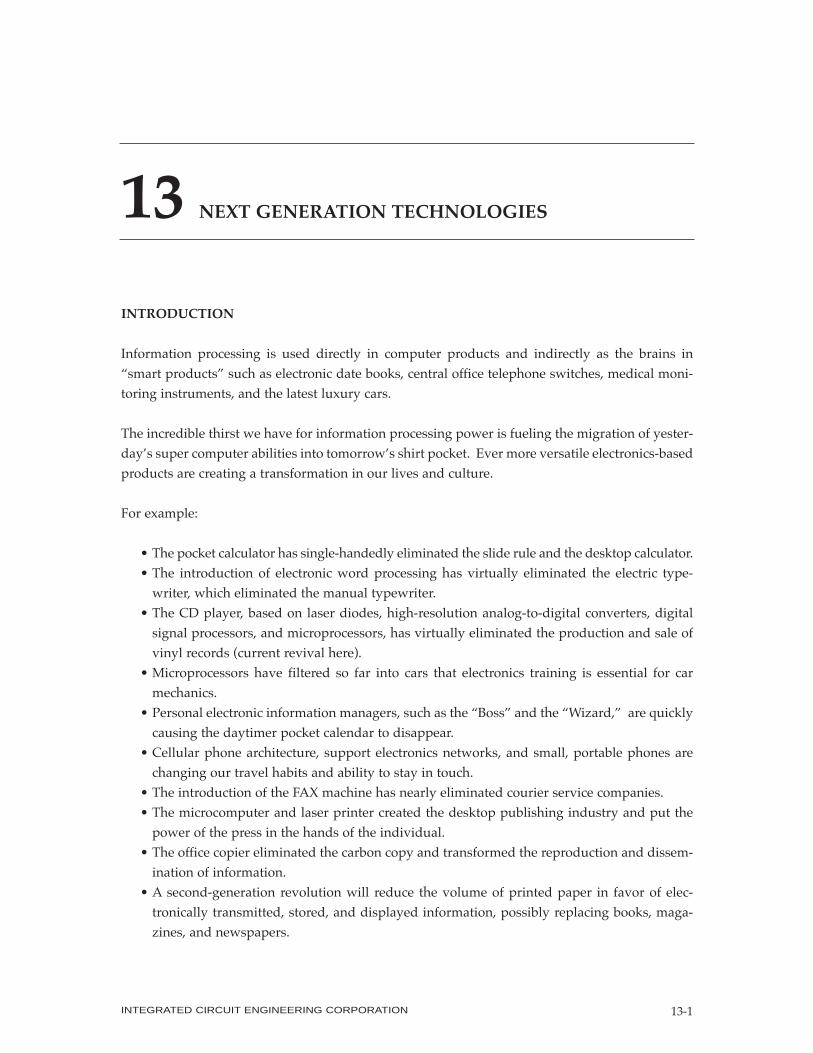
The significant advances that will be part of the future roadmaps of packaging technology in the
next five years will address the major limitations packaging imposes, illustrated in Figure 13-1.
Next Generation Technologies
INTEGRATED CIRCUIT ENGINEERING CORPORATION13-2
All of the packaging features on the future roadmap and the associated benefits have been
reviewed in this book. In addition, there are intriguing possibilities in both the packaging tech-
nologies and the information processing technologies visible on the horizon, that may signifi-
cantly impact our lives.
The packaging technologies with potential impact are related to:
¥ Getting around the high resistance of fine lines
¥ 3D packaging
¥ New materials with lower dielectric constant and photo-sensitive properties
¥ Frost MOS
¥ Enhanced thermal management
The information technologies with potential impact are:
¥ IC integration enabling system on a chip
¥ Quantum computing
¥ Molecular computing
Next Generation Technologies
INTEGRATED CIRCUIT ENGINEERING CORPORATION 13-3
Source: ICE, "Roadmaps of Packaging Technology" 22570
Packaging Challenge Packaging Roadmap Feature
I/O off the chip
Switching noise
Higher bandwidth
Wiring delay
Smaller from factors
Power dissipation
area-array bonding
low bonding parasitics
integrated decoupling caps
controlled impedance interconnect
higher packaging efficiency
higher interconnect density
higher via density
lower dielectric constant materials
3-D packaging
higher packaging efficiency withBGA, CSP, DCA and MCMs
higher interconnect density substrate
lower voltage rails
heat spreaders
water cooling
Figure 13-1. Packaging Technology Advances
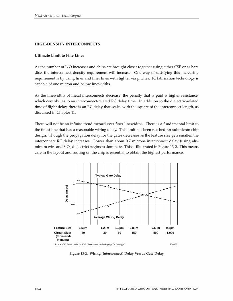
HIGH-DENSITY INTERCONNECTS
Ultimate Limit to Fine Lines
As the number of I/O increases and chips are brought closer together using either CSP or as bare
dice, the interconnect density requirement will increase. One way of satisfying this increasing
requirement is by using finer and finer lines with tighter via pitches. IC fabrication technology is
capable of one micron and below linewidths.
As the linewidths of metal interconnects decrease, the penalty that is paid is higher resistance,
which contributes to an interconnect-related RC delay time. In addition to the dielectric-related
time of flight delay, there is an RC delay that scales with the square of the interconnect length, as
discussed in Chapter 11.
There will not be an infinite trend toward ever finer linewidths. There is a fundamental limit to
the finest line that has a reasonable wiring delay. This limit has been reached for submicron chip
design. Though the propagation delay for the gates decreases as the feature size gets smaller, the
interconnect RC delay increases. Lower than about 0.7 microns interconnect delay (using alu-
minum wire and SiO2 dielectric) begins to dominate. This is illustrated in Figure 13-2. This means
care in the layout and routing on the chip is essential to obtain the highest performance.
Next Generation Technologies
INTEGRATED CIRCUIT ENGINEERING CORPORATION13-4
Del
ay (
nse
c)
1.5µm
20
1.2µm
30
1.0µm
60
0.8µm
150
0.5µm
500
0.3µm
1,000
Feature Size:
Circuit Size: (thousands of gates)
0.1
1
Average Wiring Delay
Typical Gate Delay
Source: OKI Semiconductor/ICE, "Roadmaps of Packaging Technology" 20407B
Figure 13-2. Wiring (Interconnect) Delay Versus Gate Delay

To get the most performance out of the interconnect, the intrinsic interconnect RC should be kept
a small fraction of the time of flight from dielectric delay. Consider a best case example using a
square cross section of copper with a width, w, in microns. Using a dielectric such as polyimide
or SiO2, the longest length for a trace, Lmax, in inches, for which the intrinsic interconnect RC
delay is less than the dielectric-related time of flight delay, is roughly:
With copper for example, a line six inches long should be fabricated with a width of at least 7.7
microns to avoid an excessive wiring delay. For a linewidth of three microns, a trace one inch long
will suffer a total wiring delay of 310psec, equal to twice its dielectric-related time of flight of
155psec. Three microns may be the practical limit for linewidths and thickness for thin-film mul-
tilayer interconnect substrates.
How can we break through this linewidth limitation, both for on chip and global system wiring?
Today there are three possible paths:
¥ Operating at cryogenic temperatures
¥ A hierarchy of linewidths and technologies for different trace lengths
¥ The use of superconductors
Cryogenics
The resistivities of copper and aluminum decrease with lower temperature. This is basically
because mobility and electron scattering decrease at lower temperatures. The bulk resistivities of
aluminum, copper, and several other metals versus temperature are shown in Figure 13-3. From
room temperature (298¡K) to 77¡K, the resistivities of both copper and aluminum decrease by
about a factor of 10.
This means that a copper trace could be 10 times longer at cryogenic temperatures than at room
temperature before it contributes to a doubling of the interconnect wiring delay. Likewise, traces
can be a factor of three more narrow and thinner at cryogenic temperatures and have the same
interconnect RC penalty as at room temperature.
At 77¡K, copper traces one micron in width and thickness could be practically used for intercon-
nects of one inch or less in length.
L
w10max
2
<
Next Generation Technologies
INTEGRATED CIRCUIT ENGINEERING CORPORATION 13-5

Mixed Thin Film, Cofired, and PWB
Another approach to minimizing the detrimental effect of high-resistance interconnects is to use a
mixture of narrow lines for the short traces, which are most numerous, and wider lines, with con-
sequently thicker dielectric, for the longer traces. Though the linewidth and metal thickness
determines the resistance of the line, the characteristic impedance of the line is set by the
linewidth, dielectric thickness, and the dielectric constant.
If the linewidth increases to allow lower resistance, the dielectric thickness must increase to keep
the characteristic impedance at roughly 50 Ohms. If anything, the target value of characteristic
impedance is likely to increase, requiring a further increase in the dielectric thickness. As
linewidths increase and dielectric thickness increases, at some point different via generation meth-
ods might have to be employed. This means mixing interconnect process technologies.
Next Generation Technologies
INTEGRATED CIRCUIT ENGINEERING CORPORATION13-6
0.001
1 10 100 1,000
Temperature (°K)
0.01
0.1
1
10
100E
lect
rica
l Res
isti
vity
(µΩ
•cm
)
16227ASource: "Materials at Low Temperature" by Reed and Clark/ICE, "Roadmaps of Packaging Technology"
Copper (CDA 102)
"Oxygen Free"
Aluminum (1100)
Beryllium
Brass
Stainless Steel(AlSl 300 Series)
Figure 13-3. Resistivity of Several Common Metals as a Function of Temperature

In a large multichip module most of the interconnect will be between nearby chips, requiring short
traces. These can be of the finest linewidths, possibly down to three microns. The longer traces,
such as clock lines, can be routed in layers of wider trace widths. This is effectively what is done
by NEC in the SX-X chip.
As shown in Figure 13-4, there are three interconnect technologies used with different linewidths
and length scales. Multilayer thin-film interconnect, with 25 micron linewidth on a 75 micron
pitch contains most of the signal lines in four signal layers. These layers and their three ground
planes are built on top of a multilayer, cofired base used mainly for power, ground, and clock dis-
tribution. Two of these substrates are mounted into an 18-layer printed circuit board.
The combination of ultra fine lines from thin-film technology, fine lines in BUM technology and
the low-resistance lines in the conventional PWB technology, described in Chapter 11, is also a
powerful combination offering the entire spectrum of highest possible interconnect density, yet
lowest possible interconnect delay.
Next Generation Technologies
INTEGRATED CIRCUIT ENGINEERING CORPORATION 13-7
FTCEngineering-Change Pad
PolyimideThin-Film
Layers
FTC Pad
Ground4th Signal3rd SignalGround2nd Signal1st SignalGround
Power and Ground
Ceramic BaseSubstrate
I/O PinPWB Motherboard
16228Source: ECTC '90/ICE, "Roadmaps of Packaging Technology"
Figure 13-4. Multilayer Substrate Cross Section

Superconductors
The discovery in 1986 of ceramic materials that become superconductors at 30¡K heralded a new
era for electronics. Just one year later, the liquid nitrogen barrier at 77¡K was beaten by a
YBa2Cu3O compound showing a transition temperature at 90¡K. These steady advances are dia-
grammed in Figure 13-5.
If interconnect traces are less than six inches long in a module, and linewidths of eight microns
and comparable thickness are used, then replacing the copper with a room temperature super-
conductor will not have a significant impact on the wiring delay of that module.
If this module were cooled to 77¡K, to allow the use of a ceramic superconductor, copper traces
could be as narrow as three microns before they would begin to appreciably affect the wiring
delay. This sets the upper limit to the useful regime for liquid nitrogen superconducting inter-
connects.
Next Generation Technologies
INTEGRATED CIRCUIT ENGINEERING CORPORATION13-8
160
140
120
100
80
60
40
20
0
1910 1950 1960 1970 1980 1990 2000
Year
Tem
per
atu
re (
°K)
Night timeon the Moon
Liquid Nitrogen
Surface of Pluto
Liquid Neon
Liquid Hydrogen
LeadNiobium
Niobium NitrideTriniobium Tin
Liquid Helium
TriniobiumGermanium
LanthanumBarium
Copper Oxides
YttriumBarium
Copper Oxide
MercuryBarium Calcium
Copper Oxide
Thallium BariumCalcium Copper Oxide
Bismuth StrontiumCalcium Copper Oxide
Mercury
Jan. 1987
Feb. 1987
Jan. 1988
Feb. 1988
May1993
Dec. 1986
Dec. 1986
Apr. 1986
Source: Scientific American/ICE, "Roadmaps of Packaging Technology" 22139
Figure 13-5. Sharply Rising Critical Temperatures in Superconductors Stem From the Cuprite Materials

When the interconnect density requires linewidths of less than three microns on a pitch of five
microns, a superconductor may offer better performance than copper. Two pairs of signal lines at
five microns pitch and 50 percent efficiency would offer an interconnect density of about
10,000in/in2.
At these geometries, current density becomes a major concern. Assuming a 50 ohm line and a one
volt signal level, the current through the trace is 20mA. With a three micron width and thickness,
the cross sectional area is 9 x 10⁻⁸cm2. This corresponds to a current density of over
200,000A/cm2.
In the lab, typical critical current densities before experimental superconducting materials are
quenched to normal conductivity are about 10,000A/cm2. However, highly crystalline thin films
have been fabricated that allow sustained current densities of as high as 4,000,000A/cm2. There
is nothing fundamentally preventing the use of superconductors for interconnects.
It is likely that if superconductors play a role, it will only be at the very extreme end when inter-
connect densities of more than 10,000in/in2 are needed for modules that are over three inches on
a side, and are randomly interconnected.
Of course, in addition to the development of a reliable superconductor material and deposition
process, a compatible dielectric material with low dielectric constant is essential.
3D INTERCONNECTS
Once the packaging efficiency has increased and the chips are very close together and the inter-
connect density is available to perform all the routing, it may still be possible to decrease the
wiring delay by adjusting the topology to route in three dimensions rather than two. This will
decrease the interconnect path lengths. There are a number of technologies that are aiming
toward 3D packaging.
Extension Of Conventional Approaches
The most straight-forward methods of implementing 3D packaging do not require invention of
new technologies. Some clever implementations have been available for years. An example of an
approach of small building block modular daughter cards that snap together for embedded appli-
cations from Ampro is shown in Figure 13-6. The vertical connections are made with standard
pins and connectors. The pins are on the bottom side of each modular board. On the top side of
each modular board are sockets. There is a standard bus that each board uses. Rapid prototyp-
ing is possible by just snapping boards together.
Next Generation Technologies
INTEGRATED CIRCUIT ENGINEERING CORPORATION 13-9

Another approach from Advanced Electronics Packaging uses DIMM sized modules with
memory and logic devices that plug vertically into a motherboard. An example is shown in Figure
13-7. These daughter boards in turn plug into a backplane.
Conventional peripheral packages can be stacked one on top of the other, as long as there is a bus
architecture between all the chips, and there is a means of affecting the vertical interconnect. The
Chiprack approach uses a standard chip carrier format, with approximately 88 to 132 leads. Each
Next Generation Technologies
INTEGRATED CIRCUIT ENGINEERING CORPORATION13-10
Source: Ampro/ICE, “Roadmaps of Packaging Technology” 22140
Figure 13-6. Snap-Together Mini-Modules From Ampro
Figure 13-7. Compact Solid-State Data Recorder Assembly
Source: Advanced Electronic Packaging/ICE, “Roadmaps of Packaging Technology” 22141

layer of the stack is a frame with one or more chips. These frames are stacked on top of each other
in a special connector that makes contact with the one above it. An example of a frame and a 6
chip stack composed of a 68070 processor, ASIC, ROM and RAM, is shown in Figure 13-8.
Dense-Pac offers memory modules with stacks of custom ceramic single chip layers interconnected
along their edges with solder. Examples of the companyÕs module is shown in Figure 13-9. Each
stackable leadless chip carrier (SLCC) starts as a bare die, mounted into a custom ceramic leadless
package with castillations around the edges. The chip is assembled into the package and wire-
bonded in place. The lid is sealed and the unit is tested.
In the typical SRAM applications, the enable line on each chip in a stack must be unique. This is
programmed by cutting out links on the outside of the package before the SLCCs are stacked. The
SLCCs are then solder dipped to connect the edges. This process flow is shown in Figure 13-10. The
bottom footprint can be a PGA, gull wing or J lead, by changing the bottom package configuration.
Next Generation Technologies
INTEGRATED CIRCUIT ENGINEERING CORPORATION 13-11
Source: Applied Research and Consultancy Centre/ICE, “Roadmaps of Packaging Technology” 22142
a
b
Figure 13-8. Stacked Chip Carriers

Next Generation Technologies
INTEGRATED CIRCUIT ENGINEERING CORPORATION13-12
Source: Dense-Pac Microsystems/ICE, “Roadmaps of Packaging Technology” 22143
Figure 13-9. Dense-Pac 3D Memory Modules
Figure 13-10. Dense-Stack Assembly Flow Stackable Leadless Chip Carrier (SLCC)
22144Source: Dense-Pac Microsystems, Inc/ICE, "Roadmaps of Packaging Technology"
Chip
Special CeramicPackage
Mount/Wirebond
Lid
Seal
SLCC(Stackable Leadless
Chip Carrier)
(Bottom View) #8 Position
ProgramPackage To
#1 Position #2 Position
EnvironmentalScreeningCentrifuge
Temp. CycleFine/Gross Leak
TestBurn-InTestInventory

Vertical module stacking allows dramatic board area reduction. Figure 13-11 compares the
board area needed to assemble 128 chips in various package styles. The standard SOIC form
factor takes up about 65 square inches of board space. Sixteen, 8 high stacks would take up less
than 10 square inches.
Staktek uses a similar method, but with plastic packaged chips. Each die is mounted in a molded
plastic unit with leads out two sides, as shown in Figure 13-12. These can use a standard TSOP
style or a customized part with half the thickness. These layers are then stacked, 4-8 chips high
and held in place with a metal frame. The frame is then soldered to the package leads. With the
ultraslim module, 512 chips can be assembled to a card less than 4 inches by 8 inches. An exam-
ple of a double sided memory card used by Cray Research and assembled by Celestica is shown
in Figure 13-13.
Stacking Bare Die
Methods pioneered by TI and Irvine Sensors involve creating a ÒcubeÓ of functional silicon. An
example of Irvine SensorsÕ design is shown in Figure 13-14. So far, this technology has been
applied to memory chips, which require low interconnect densities. A metallization layer is added
to a wafer of standard dice to bring all the leads to one side of each die. The wafer is thinned to
six mils, and the chips are diced.
Next Generation Technologies
INTEGRATED CIRCUIT ENGINEERING CORPORATION 13-13
Pac
kag
e Ty
pe
0 25 50 75 100 125
128 DIP's
128 SOIC's
128 SOJ's
128 LCC's
64 - 2 High Stacks
32 - 4 High Stacks
16 - 8 High Stacks
PCB Area (in2)Source: Dense-Pac Microsystems, Inc./ICE, "Roadmaps of Packaging Technology" 22145
Figure 13-11. Comparisons of PCB Space Required for a 16MB SRAM Systemfor Different Package Types

Good dice are laminated together into a cube using epoxy. The edge with the leads is lapped
down to expose the pads, which are connected and finally solder dipped to provide the vertical
connections. The cube is soldered to a base plate that converts the side connections to a pad array.
Solder balls on the base turn the cube into a BGA. An example of a short stack, a tall stack and
the base are shown in Figure 13-15.
TI has developed a similar process. It uses a TAB-like leadframe deposited on top of the die and
overhanging the edge, transforming the standard peripheral leads into edge tabs. Chips are glued
together into a cube with the tabs sticking out, which are also soldered to a substrate. An exam-
ples of an MCM using their memory cubes is shown in Figure 13-16.
Next Generation Technologies
INTEGRATED CIRCUIT ENGINEERING CORPORATION13-14
Source: Staktek/ICE, "Roadmaps of Packaging Technology 22146
I.C. DIE DISCRETE I.C. PACKAGE STAKPAKS
Figure 13-12. Staktek 3D Memory Modules
Figure 13-13. 1 Gigabyte Card Assembled by Celestica and Used by Cray
Source: Celestica/ICE, “Roadmaps of Packaging Technology” 22147

Issues related to thermal management, manufacturing, and reliability still need to be worked out.
However, the memory density possible is very considerable. A RAM module with a footprint of
less than one square inch could hold over 32 die. If each one were a 64M DRAM, this module
would store 256Mbytes of memory.
Next Generation Technologies
INTEGRATED CIRCUIT ENGINEERING CORPORATION 13-15
Source: Irvine Sensors Corporation/ICE, “Roadmaps of Packaging Technology” 16443A
Figure 13-14. Irvine Sensors 3D Cube
Figure 13-15. Stacked Memory Module
Source: Irvine Sensors/ICE “Roadmaps of Packaging Technology” 22148

Stacking MCMs and Boards
TI has extended this notion to include the stacking of multichip modules. This is shown in Figure
13-17. Connections are brought out to the edge of each substrate and interconnected by a moth-
erboard, which can be a thin-film multilayer substrate.
Button Board
A limitation to the above approach to 3D interconnection is the need to provide connections along
the edge of the module in a single row only. This is simply a scaled-down version of the tradi-
tional approach of printed circuit cards plugged into a common backplane. The reason it has not
been adopted by IBM, NEC, or DEC, for example, instead of one or two large planar printed cir-
cuit boards, is the limit in the number of connections available between boards.
One approach to provide a greater number of contacts between boards, while distributing the con-
tacts over the area of the device rather than just around the periphery, is to use the ÒButton
Contact.Ó It has been extensively used by TRW and is available commercially from Tecknit. An
example of TRWÕs board is shown in Figure 13-18.
Next Generation Technologies
INTEGRATED CIRCUIT ENGINEERING CORPORATION13-16
Courtesy of Texas Instruments. This 3-D packaging technology was developed by 16552ATexas Instruments under the sponsorship of the U.S. Department of Defense’sDefense Advanced Research Project Agency (DARPA).
Figure 13-16. TI Cube MCM

The basic element of a button contact is a short length of wire that has been randomly twisted and
bent into the shape of a cylinder, typically 20 to 50mils in diameter, and twice as long as it is wide.
The wire, from 0.5mil to 5mils in diameter, is composed of copper, beryllium-copper, tungsten, or
stainless steel, which has been gold plated. Examples of the wire buttons are shown in Figure 13-19.
These buttons are inserted into insulated holes of slightly smaller diameter and act as conductive,
compliant interconnects between flat surfaces. In the boards developed by TRW, the interconnects
have been mated and de-mated hundreds of times with no effect on the signal integrity.
The use of button contacts may allow an area array of contacts between modules for a truly high-
density, 3D interconnected structure. These contacts are used in BGA and LGA sockets as well.
NEW ELECTRONIC MATERIALS
The driving force of reducing the wiring delay of the interconnects is also influencing the intro-
duction of lower dielectric constant materials. As mentioned in Chapter 11, glass-ceramics that
have dielectric constants from 5.8 to 7.0 are beginning to appear as LTCC. These materials will be
replacing the 90 to 95 percent alumina with dielectric constants over 10 that have been used for
cofired ceramics for over 30 years.
Next Generation Technologies
INTEGRATED CIRCUIT ENGINEERING CORPORATION 13-17
2"
3/4"
Memory Slots
Microprocessor SlotsSilicon Rack
Source: TI/ICE, "Roadmaps of Packaging Technology" 14742A
• Uses Custom Substratesas Mini-PWB
• Preferential Etch Slotsin Silicon Rack forWafer Cards
• Assembly and ReflowConnections BetweenRack and Mini-PWBs
• Hermetic ConstructionAllows Direct Cooling
Figure 13-17. 3D Packaging of MCM Modules

For polymer-based printed wiring boards, fluoropolymer materials are being introduced. Teflon
has the lowest dielectric constant of any solid, homogeneous material, at about 2.0. The same non-
polar and low polarizability of its molecular structure that keeps its adhesion so low, also keeps
its dielectric constant low.
This value of dielectric constant represents the basic polarizability of the electronic structure of the
polymer chain. The polymer chains are so symmetrical, and the C-F bonds hold its electrons so
tightly, that they do not easily contribute to either van der Waals forces with foreign atoms, or
polarization from external fields.
As mentioned in Chapter 11, fluoropolymer PWB laminates are available from Gore, DuPont,
and Rogers with fillers added to enhance their mechanical properties and manufacturability in a
PWB process. The dielectric constant is increased up to approximately 2.9 depending on the filler
material.
Next Generation Technologies
INTEGRATED CIRCUIT ENGINEERING CORPORATION13-18
• Extremely short second-and third-level interconect (high-speed)• Interconnect boards can be added to accommodate wiring
changes, unit growth, or flexible module applications• No edge-card connectors or backplane wiring• Test boards can be used at the module and system levels
to access all interconnects• Conductive thermal management for all components
(bolted interfaces)• Feed-through spacers can be adjusted in thickness to minimize
board (module) spacing and unit size• Data bus is located for common impedance to all chips• Only pressure required to assemble unit• Interconnect is easily changed to accommodate system
growth, changes, etc.
Clamp
InterconnectBoardsComponent
InterconnectBoards
InterconnectBoards
Mounting Boards
Button Board
Button BoardFeed-ThroughSpacer
Feed-ThroughSpacer
Test Board
Heat Sink (Typical)
ComponentMounting
Spacer Board
Contact FlushSurface
Insulator
Conductive PlugsGold Plated
Base Plate"Heat Exchanger"
Superchips
Heat SinkBase Mounting
Button Boards(Typical)
Clamp Structure
Through Bolt(Typical)
Spacer Board
InterconnectMulti-Layer Board
Unit I/O Structure
Source: TRW/ICE, "Roadmaps of Packaging Technology" 13860A
Figure 13-18. 3D Packaging

Up to recently, fluoropolymer materials have been suitable only for use as laminates, and limited
to thickness greater than three mils. DuPont has recently announced a Teflonª material that can
be spin coated. Termed Teflon AF for ÒAmorphous Fluoropolymer,Ó it can be spun onto wafer
substrates in micron-thick films. Patterning methods based on laser ablation or plasma etching as
well as metal adhesion still need to be fully developed. Teflon AFÕs very low dielectric constant
of about 1.9 and ability to form thin films makes it an attractive material.
Another approach to low dielectric constant has been tried by nCHIP, based on structure rather
than materialsÕ engineering. It has often been said that a microstrip transmission line is ÒfasterÓ
than a stripline structure. This is because the electric field of a microstrip extends into the air above
the trace, and the contribution from the air lowers the effective dielectric constant of the trace.
In a stripline geometry, the electric field is fully contained within the dielectric and the effective
dielectric constant is the bulk dielectric constant of the material.
nCHIP has applied this principle of fringe fields in air decreasing the effective dielectric constant
in its ÒIsostrip,Ó or Isolated Microstrip Transmission lines. A microstrip structure is used with all
the dielectric material not directly under the trace removed. This increases the field that is in air,
reducing the effective dielectric constant. Figure 13-20 shows a cross section of an Isostrip trace.
The effective dielectric constant is reduced to 1.9 using this configuration.
Next Generation Technologies
INTEGRATED CIRCUIT ENGINEERING CORPORATION 13-19
Source: IEPS 1990/ICE, "Roadmaps of Packaging Technology" 16232
Figure 13-19. Wire Button Design

In addition to performance, as related to decreased wiring delay, another driving force on new
materials is reduced manufacturing time and cost. Photosensitive polymers offer the possibility
of eliminating half of the polymer processing steps. For example, the Probimide photosensitive
polyimides from Ciba-Geigy Corp., have been used to fabricate thin-film multilayer structures
with the vias created in the polyimide by direct imaging from a mask. This process is outlined in
Figure 13-21.
FROST-MOS: CYRO-COOLING OF CMOS
In CMOS-based systems, a large source of critical net propagation delay is the intrinsic gate delay.
This is continually being reduced as feature sizes are made smaller. In addition, it can be lowered
by cooling the devices.
The other dominant source of propagation delay is the intrinsic RC delay of the interconnect. As
pointed out in a previous section of this chapter, this can also be decreased by an order of magni-
tude by cooling the chip.
In Figure 13-22, the clock frequency versus temperature for a single-chip CMOS microprocessor is
shown. This indicates that if the clock is running at 15MHz with a junction temperature of 125¡C
(398¡K), cooling it down to 80¡K will result in a clock frequency of 35MHz, a 2.3x improvement.
ETA applied this principle in the ETA-10 by immersing an entire CPU board containing over 200
CMOS gate arrays in liquid nitrogen dewar. Speed increases of from 2 to 5 over room tempera-
ture operation were reported.
Next Generation Technologies
INTEGRATED CIRCUIT ENGINEERING CORPORATION13-20
Silicon Substrate
Metal
16231
SiO Dielectric2
Power Plane
ReducedFringe
Capacitance
Source: nChip/ICE, "Roadmaps of Packaging Technology"
Figure 13-20. Isolated Microstrip Transmission Lines

On a smaller scale, a micro-refrigerator technology is available from MMR Technologies. An early
prototype, shown in Figure 13-23, can extract one watt while keeping a chip at 82¡K. This first
prototype was built in a 40-pin ceramic DIP.
These refrigerators use the Joule-Thomson effect, in which the expansion of a gas extracts heat.
Pressurized gas enters the module, and through the use of precisely shaped channels, low-pres-
sure, chilled gas contacts the cold plate where the chip is mounted.
Next Generation Technologies
INTEGRATED CIRCUIT ENGINEERING CORPORATION 13-21
Conventional Process Photosensitive Process
Coating ofPolyimide
Coating ofPhotoresist
Polyimide
Photoresist
Light
CuredPolyimide
StrippedPhotoresist
EtchedPolyimide
DevelopedPhotoresist
Exposure
Photoresist Polyimide Coating ofPhotoresistPolyimideSubstrate
Mask
Exposure
DevelopedPolyimide
CuredPolyimide
16230Source: Ciba Geigy/ICE, "Roadmaps of Packaging Technology"
Figure 13-21. Polyimide Pattern Generation Processes

Next Generation Technologies
INTEGRATED CIRCUIT ENGINEERING CORPORATION13-22
0 100 200 300 400
Temperature (°K)
0
10
20
30
40
16233
5
15
25
35
50 150 250 350
Fre
qu
ency
(M
Hz)
Source: ICE, "Roadmaps of Packaging Technology"
Figure 13-22. Speed of CMOS Clock as a Function of Temperature
Figure 13-23. Single-Chip Cryogenic Cooler
Source: MMR Technologies Inc./ICE, "Roadmaps of Packaging Technology" 16226

Superconductor Technologies Inc. (STI), has introduced a cooler for chilled CMOS module appli-
cations. Called the Radically Accelerated Cold Electronic (RACE) refrigeration system, it is 5 in x
5 in x 12 inches and handles a heat load of 30 watts at a temperature of Ð25¡C. At this tempera-
ture, it is estimated there is a 60% increase in frequency for core limited CMOS. An example of
the RACE 30 is shown in Figure 13-24. The chilled CPU is actually in the external chamber, con-
nected to the rest of the computer by a ribbon cable.
The RACE cooler operates based on
the Sterling cycle of compressing
and expanding a gas. There are
three versions, the RACE 30 cools to
Ð25¡C, the RACE 60 cools to Ð55¡C
and the RACE 77k can pump 4
watts at 77¡K. An example of the
RACE 77k is shown in Figure 13-25.
Through the use of such localized
coolers, the critical chips in a
CMOS-based CPU could be cooled
to decrease the gate delay of a cur-
rent generation technology to that of
a few generations in the future. This
could mean a few yearsÕ jump in the
time to market for a new CMOS-
based workstation or server.
Next Generation Technologies
INTEGRATED CIRCUIT ENGINEERING CORPORATION 13-23
Source: Superconductor Technologies Inc./ 22150ICE, “Roadmaps of Packaging Technology”
Figure 13-24. RACE 30 Workstation CPU Cooler
Figure 13-25. RACE 77k Stirling Cycle Cooler
Source: Superconductor Technologies Inc./ 22149ICE, “Roadmaps of Packaging Technology”

THERMAL MANAGEMENT
At the very high end, both the power densities generated by the individual devices and the result-
ing power densities generated by the CPU boards are increasing. For example, the MCA III cur-
rently has a power density at its surface of greater than 200W/in2. The CPU of a large mainframe
or super computer can contain about 1 million gates. If each of these gates dissipates about 3mW
of power, the cooling for the CPU must allow the extraction of 3kW of power.
Two methods will see growing application: the use of high thermal conductivity heat spreaders to
transport the heat from the die itself to a cooling medium. The second method uses a cooling
fluid, possibly water or some other chemical, to remove heat from the system.
In the DEC VAX 9000, the heat spreader is a block of copper to which the dice are directly attached,
using electrically insulating, but thermally conducting, epoxy, filled with diamond powder. In the
Motorola/Siemens multichip modules, the backsides of the dice are pressed to a polished and
anodized aluminum plate. In both cases the metal plates spread the heat to a larger area for
extraction Ñ using air for the VAX 9000, water for the Motorola/Siemens module.
Another attractive heat spreader material is aluminum nitride. When processed with a minimum
oxygen content, it can have a thermal conductivity approaching aluminum metal, 2.3W/cm¥¡C.
Figure 13-26 shows the thermal conductivity dependence on the oxygen content. Processing of
aluminum nitride will require careful control.
Aluminum nitride offers the special advantage of allowing multilayer interconnect when cofired
with tungsten, for example. Coors and WR Grace are developing an aluminum-nitride/tungsten
cofired process. Toshiba has built a number of multilayer, multichip modules with cofired alu-
minum nitride, using the substrate as the integrated heat spreader.
The further advantage of aluminum nitride is the good TCE match with silicon and the possibil-
ity of allowing a true hermetic seal to enclose the chips.
As pointed out in Chapter 6, when air is used as the thermal extraction medium, it offers a best
case thermal resistance of 100¡C/watt for a 1in3/sec flow. To extract 3kW of power with a 25¡C
case-to-ambient temperature drop would require a flow rate of 12,000in3/sec, which is approxi-
mately 7ft3/sec. In moving through an aperture 6 inches wide by 4 inches high, the air velocity
would have to be about 30 miles per hour!
Next Generation Technologies
INTEGRATED CIRCUIT ENGINEERING CORPORATION13-24

As power densities increase, water cooling will tax the engineering heroics less than air cooling,
and may result in a lower cost system. Extracting 3kW of heat under the same conditions as above
with water cooling requires only 4in3/sec of water. The Motorola/Siemens module has integrated
water cooling channels in the aluminum heat spreader. NTT has proposed integrating cooling
channels in the cofired ceramic interconnect substrate, as shown in Figure 13-27.
Next Generation Technologies
INTEGRATED CIRCUIT ENGINEERING CORPORATION 13-25
7.00 1.0 2.0 3.0 4.0
0
0.5
1.0
5.0 6.0
2.5
2.0
1.5
2.3 Aluminum Metal
Oxygen Impurity (Weight %)
Th
erm
al C
on
du
ctiv
ity
(W/c
m•°
K @
300
°K)
16237Source: International Journal of Hybrid Microelectronics/ICE, "Roadmaps of Packaging Technology"
Figure 13-26. Thermal Conductivity Dependence on Oxygen Impurity in AlN
Figure 13-27. NTT Water-Cooled Cofired Aluminum Nitride Substrate Packaging Concept
Source: 36th ECC Conference, 1986/ICE, "Roadmaps of Packaging Technology" 16229A
H20Chip
CoolingPassages
CoolingManifold
RearInterconnectionPads
Piping
MultichipPackage
I/OConnector
WiringBoard
InterconnectionPads
MLCSubstrate

Yet another application for cryo-cooling of CMOS is for enhanced heat extraction. Liquid nitro-
gen can be used as a cooling medium by its heat of vaporization. If a chip or module is immersed
in liquid nitrogen and if the nitrogen fluid is flowing over the surface, to minimize the boiling film,
large heat fluxes can be removed and the surface can be kept at low temperature. Figure 13-28 is
an example of the heat fluxes that can be removed in a simple arrangement of a stream of liquid
nitrogen, cooled to 68¡K, 9 degrees below its boiling point, impinging on a heated chip. 80
watts/cm2 have been demonstrated, with a rise in temperature of only 20 degrees above the nitro-
gen temperature of 68¡K. This approach may easily remove over 200 watts/cm2 while keeping
the junction temperature well below 0¡C.
SILICON ADVANCEMENTS: SYSTEM-ON-A-CHIP
A high-end CPU may need at most only 10 million transistors. By the year 2000, 100 million tran-
sistor chips will be fabricated. What will the extra gates be used for? One proposal is to integrate
all the features of the system on a single chip. This includes RAM, ROM, EPROM, disk and
peripheral controllers, multimedia, 3D graphics, communications, and DSP functions.
The first trend in this direction is the introduction of DRAM with on-chip microprocessors. In this
low-end case, the chips are dominated by memory, with a relatively small area taken up by the
logic functions. In this case, it is really a microprocessor embedded on a DRAM. An example of
the architecture and implementation of the M32R/D from Mitsubishi is shown in Figure 13-29. It
consists of 2Mbits of DRAM and a 32 bit microprocessor. It targets embedded applications.
Next Generation Technologies
INTEGRATED CIRCUIT ENGINEERING CORPORATION13-26
0.06 I/min0.11 I/min
0 5 10 15
Tchip,ave – Tjet (°K)
Po
wer
Flu
x F
rom
Su
rfac
e (W
/cm
2 )
20 25 30
100
90
80
70
60
50
40
30
20
10
0
Source: IEEE/ICE, "Roadmaps of Packaging Technology" 22151
Figure 13-28. Constant Flow Rate Liquid Nitrogen Jet Impingement With 8.8¡K Subcooling

IBM has converted an 8 chip MCM with over 1,000 pins into a single chip, with 15 million tran-
sistors, using 0.25 micron technology. It is packaged into a ceramic BGA with a 42.5mm body size
and dissipates 30 watts. This part is used in the RS/6000 workstation as well as the SP-2 super-
computer.
The transition toward systems-on-a-chip will be driven by the availability of 100 million transistor
ASICs. This will radically change the way systems are designed. There are specialized companies
that only supply DRAMs or only supply MPEG decoders, or only supply peripheral chip sets.
In the conventional system design approach, each company could specialize and provide a clean
interface to the system designer in a single chip package. The design of MCMs caused complica-
tions when more than one companiesÕ chips were to be included. Who took responsibility if a chip
was bad, or didnÕt meet specifications?
In designing a system-on-a-chip, who will supply the design information for all the system com-
ponents, or cores, that will go on the single chip? Recognizing that there are new relationships that
must be forged in the industry to support the technical features that will be soon available, a new
industry alliance has emerged, called the Virtual Socket Interface, VSI. This group is composed of
Next Generation Technologies
INTEGRATED CIRCUIT ENGINEERING CORPORATION 13-27
512byteCache
512byteCache
Buffers Buffers
128 128TAG
DRAMControl,
Etc.
BusInterface
MemoryController
32
512byteCache
512byteCache
Buffers Buffers
128 128
DRAMControl,
Etc.
Clock BusInterface
32 x 16bitMultiplexer-Accumulator
Datapath Control
M32R/D CPU
512KbyteDRAM
512KbyteDRAM
512KbyteDRAM
512KbyteDRAM
Source: Electronic Products/ICE, “Roadmaps of Packaging Technology” 22152
Figure 13-29. Logic Area in MitsubishiÕs Microprocessor-on-a-DRAM

representatives from the EDA design community, the semiconductor vendors, the core design
vendors, and the system end users. A list of the current membership is shown in Figure 13-30.
The excitement over the birth of the system-on-a-chip and the role that the VSI alliance may play
in the industry has been put to verse in Figure 13-31.
The introduction of the system-on-a-chip will have significant impact on packaging as well. As
the functional integration increases, there is a point where the I/O needs of the chip start to
decrease. When the entire system is integrated on one chip, the I/O demands should eventually
be limited to power and ground distribution and a few narrow busses for input and output, such
as video drivers, keyboards and speaker drivers. Packaging may be relegated to the role of phys-
ically embedding the systems-on-a-chip into the system, rather than focusing on interconnecting
higher and higher pin count devices. The new technologies that are being driven by the current
demands for smaller package form factor, higher via density and higher interconnect density may
have a limited future.
Next Generation Technologies
INTEGRATED CIRCUIT ENGINEERING CORPORATION13-28
EDA Vendors
Aspec
Cadence
Compass
Mentor
Summit
Synopsys
Viewlogic
VLSI Libraries
Semiconductor Vendors
Actel
Alcatel-Mietec
Altera
Cirrus Logic
Fujitsu
Hitachi
National
NEC
Texas Instruments
Toshiba
TSMC
VLSI Technology
Xilinx
Intellectual-Property Vendors
Advancel Logic
ARM
CompCore Multimedia
DSP Group
Excellent Design
Integrated Silicon Systems
iReady
Object Oriented Hardware
Phoenix
PrairieComm
Rapid*
Sand
Sun/Java
3Soft
VLSI Libraries
Systems Vendors
Alcatel
Silicon Graphics
Sun
Sony
*Rapid is a consortium of intellectual-property vendors
Source: EE Times/ICE, "Roadmaps of Packaging Technology" 22153
Figure 13-30. Virtual Socket Interface Member Companies

LIMITS TO SILICON: QUANTUM COMPUTING
When the physical size of a transistor gets below 0.1 micron, it contains less than a million atoms.
The behavior of junctions changes radically in this size regime. After all, the statistical fluctua-
tions of carrier concentrations from a doping level of 1ppm will result in less than half of all the
channels having no minority atoms!
In this size scale, with structures about 1,000 atoms wide, macroscopic quantum effects dominate.
The vision slowly emerging of what a transistor will look like below 0.1 micron feature size is that
of a quantum dot. A single, isolated island of conductor will act as a confining trap for a single
electron. The conductor might be a GaAlAs heterostructure. One possible design of a quantum
dot logic element is shown in Figure 13-32.
Next Generation Technologies
INTEGRATED CIRCUIT ENGINEERING CORPORATION 13-29
What's this news, this ballyhoo,this concept couched in hullabaloo?From California comes the tip:the longed-for system-on-a chip!What once was merely a fantasymay soon become reality;there's an Alliance now in place—the Virtual Socket Interface,Providers of so-called IP(that's intellectual property),design software and such as these—also systems companies—decided to cooperatein order to acceleratethe growth of this new industrycombining logic, memoryand peripherals as wellon one lone chip. It's bound to sell!
Of course this course, till now uncharted,faces hitches getting started;There's no need for apologywhen problems of technologyare among the reasons whymemory and logic on one dieare not easy to combinein a snazzy new design.But this process, till now thwarted,will by no means be aborted;thanks to the VSIAthe project is well underway.It may even be arrangedto have macros interchanged,without overwhelming slips,between firms that create the chipsfor many kinds of application.Bravo for cooperation!
May progress come from this alliance(on which we place such reliance),and much profit from its wisdom.Let's hear it for the one-chip system!Source: Carolyn Sobel/ ICE, "Roadmaps of Packaging Technology"
22154
Figure 13-31. Chip Chip Hurray Ð By Carolyn Sobel

A quantum dot that contains one bit of information has been termed a quantum bit or ÒqubitÓ. In
the qubit illustrated above, there are five stable locations for a free electron to be located: the four
corners, and the middle.
In an array of adjacent quantum dots, each would be loaded with two electrons. Though no elec-
tron would propagate between quantum dots, the location of the two electrons in each dot is
dependent on the proximity of the electron in adjacent dots. When the state is changed at one end
of the chain of quantum dots, other dots down the line might change as a result, depending on the
logical operation. For example, Figure 13-33 illustrates a stable pattern of a three input gate. The
majority value of the inputs is transmitted to the output.
In Figure 13-34, an example of how this structure could be turned into a programmable gate is
illustrated. The principles of quantum computing are just now being developed in anticipation
for the period 10 years from now when the limits to conventional semiconductor operation will
be reached and quantum computing might be required.
Next Generation Technologies
INTEGRATED CIRCUIT ENGINEERING CORPORATION13-30
TrappedElectron
TunnelingBarrier
Outer Cell WallTraps Electrons
CenterQuantum
WellCorner
QuantumWell
Logic 0 Logic 1Source: Notre Dame University/ICE, "Roadmaps of Packaging Technology" 22155
Figure 13-32. Quantum Dot Bistable Logic Element
Figure 13-33. The ÒMajority WinsÓ Principle in Qubit Logic
22156Source: Notre Dame University/ ICE, "Roadmaps of Packaging Technology"
1 1
1
0

The limits of quantum computing may be when individual molecules are encoded with informa-
tion. The Buckministerfullerene molecule, C60, offers an intriguing possible molecule to manipu-
late. IBM has demonstrated the positioning of Buckyballs on a copper surface. Rows of 10
Buckyballs were lined up in grooves on a copper plate, using a scanning tunneling microscope tip.
By careful positioning, the balls mimic an abacus. However, this abacus, shown in Figure 13-35,
is only 10 x 40nm on a side. No one has proposed Òabacus computingÓ on the molecular level.
However, this feat demonstrates what might be possible.
Next Generation Technologies
INTEGRATED CIRCUIT ENGINEERING CORPORATION 13-31
22157Source: Notre Dame University/ICE, "Roadmaps of Packaging Technology"
ProgramLine
(Held in"1" State)
Input A = 1
Input B = 0
Output C = 1
Figure 13-34. A Possible Qubit Programmable Logic Element
Figure 13-35. A Molecular Abacus Using Buckyballs
Source: IBM/ICE, "Roadmaps of Packaging Technology" 22158

BEYOND QUANTUM COMPUTING: DNA COMPUTING
Molecular computing in a biological cell proceeds continuously and at a furious pace. One cell,
approximately 5 microns on a side, has approximately 1 trillion molecules. Each of these mole-
cules has combinatory rules of interaction. Harnessing the computing power of biologically active
molecules has been demonstrated by computer scientist Leonard Adleman of the University of
Southern California in Los Angeles. He used the DNA molecule as the computing engine to solve
a specific problem.
DNA is composed of sequential nucleotide segments, each one strung across a rung in a double
helix pattern. An example of a 10 segment DNA molecule is shown in Figure 13-36. There are
four basic nucleotides, symbolized by the letters A, T, C and G. Information is encoded in a strand
of DNA by the order of the nucleotides. The problem Aldeman was able to solve is often called
the traveling salesman problem:
There are seven cities, and a total of 14 one way flights between the cities. What is the path a
salesman can take to travel starting at a specific city and ending at a specific city while passing
though each of the other cities only once.
Aldeman encoded each of the cities as a 20 segment nucleotide. He then created a complimentary
segment of nucleotides that would attach to each one of the 20 nucleotide cities. To form the 14
one way flights, he synthesized DNA sequences that had the last 10 nucleotides of the origin city
and the first 10 segments of the destination city.
Next Generation Technologies
INTEGRATED CIRCUIT ENGINEERING CORPORATION13-32
Source: Science News/ 22159ICE, “Roadmaps of Packaging Technology”
Figure 13-36. Short Segment of a DNA Molecule, With 10 Nucleotide Segments

Next, he added pinches of these 21 powders: 14 one way flight segments and 7 city compliment
segments, to a test tube of water, where they dissolved. With all the molecules free to interact with
each other, the city complements would bind to the ends of the one way link segments, forming
all possible chains.
The information encoding was in the nucleotide segments for each city and one way link. The
combination rules were encoded by the choice of the nucleotide sequences and the nature of the
A, T, C, and G chemistry. The information processing was the chemical reaction that created all
possible one-way-link-city-one-way-link polymer chains that the segments and encoding rules
allowed. The interpretation of the information relied on finding the resulting chain that was
exactly (7 cities) x (20 nucleotides per city) segments long, had the right start-and-end segments
and did not have repetitious segments. These were found by electrophoresis.
The resulting DNA segment chain with the path through the 7 cities encoded in it was then read
out. The answer is shown in Figure 13-37. This shows the 7 cities, the 14 one way links, and the
complete path proceding from city number 0 to city number 6.
It is not clear what the future of DNA computing is, even if there is a future, or whether this one
example of DNA computing is a novelty. However, the interest has started molecular geneticists
talking to computer scientists. Many outcomes may result from this association.
FINAL COMMENTS
For as long as machines require ever more powerful microprocessors, technology will steadily
advance and packaging technology will continue to play catch-up.
Next Generation Technologies
INTEGRATED CIRCUIT ENGINEERING CORPORATION 13-33
0
1
2
3
4
5
6
Source: Science News/ICE, "Roadmaps of Packaging Technology" 22160
Figure 13-37. Unique Hamiltonian Path

The myriad of packaging choices available today will be a part of the portfolio of solutions for all
electronic products for years to come. After all, DIPs, which are over 30-years old, are still today
an integral part of many electronic products.
The next generation solutions will arise from natural engineering extensions and creative combi-
nations of new designs, new materials, and new processes for the ultimate goal. As summarized
in Figure 13-38, this goal involves packing higher performance in a smaller volume at lower cost,
or in other words, developing systems that are Ò...faster, smaller, less expensive, NOW.Ó
Next Generation Technologies
INTEGRATED CIRCUIT ENGINEERING CORPORATION13-34
“We’ve finally paid up on this $300,000 baby,and now they’ve come up with one that can do the same job
for $79.95.”© 1982 by Sidney Harris - “What’s So Funny About Computers?”, William Kaufmann, Inc. 16238
Figure 13-38. Next-Generation Computing Patterns