14th workshop on crystalline silicon solar cells & modules ... · 14th workshop on crystalline...
TRANSCRIPT

14th Workshop on Crystalline Silicon Solar Cells & Modules: Materials and Processes Extended Abstracts and Papers
August 2004 • NREL/BK-520-36622
Workshop Chairman/Editor: B.L. Sopori Program Committee: J. Kalejs, J. Rand, T. Saitoh, R. Sinton, M. Stavola, D. Swanson, T. Tan, E. Weber, J. Werner, B. Sopori, and M. Al-Jassim Winter Park Mountain Lodge Winter Park, Colorado August 8-11, 2004
National Renewable Energy Laboratory 1617 Cole Boulevard, Golden, Colorado 80401-3393 303-275-3000 • www.nrel.gov
Operated for the U.S. Department of Energy Office of Energy Efficiency and Renewable Energy by Midwest Research Institute • Battelle
Contract No. DE-AC36-99-GO10337
14th Workshop on Crystalline Silicon Solar Cells & Modules: Materials and Processes Extended Abstracts and Papers
August 2004 • NREL/BK-520-36622
Workshop Chairman/Editor: B.L. Sopori Program Committee: J. Kalejs, J. Rand, T. Saitoh, R. Sinton, M. Stavola, D. Swanson, T. Tan, E. Weber, J. Werner, B. Sopori, and M. Al-Jassim Winter Park Mountain Lodge Winter Park, Colorado August 8-11, 2004 Prepared under Task No. WO97.D999
National Renewable Energy Laboratory 1617 Cole Boulevard, Golden, Colorado 80401-3393 303-275-3000 • www.nrel.gov
Operated for the U.S. Department of Energy Office of Energy Efficiency and Renewable Energy by Midwest Research Institute • Battelle
Contract No. DE-AC36-99-GO10337

NOTICE
This report was prepared as an account of work sponsored by an agency of the United States government. Neither the United States government nor any agency thereof, nor any of their employees, makes any warranty, express or implied, or assumes any legal liability or responsibility for the accuracy, completeness, or usefulness of any information, apparatus, product, or process disclosed, or represents that its use would not infringe privately owned rights. Reference herein to any specific commercial product, process, or service by trade name, trademark, manufacturer, or otherwise does not necessarily constitute or imply its endorsement, recommendation, or favoring by the United States government or any agency thereof. The views and opinions of authors expressed herein do not necessarily state or reflect those of the United States government or any agency thereof.
Available electronically at http://www.osti.gov/bridge
Available for a processing fee to U.S. Department of Energy and its contractors, in paper, from:
U.S. Department of Energy Office of Scientific and Technical Information P.O. Box 62 Oak Ridge, TN 37831-0062 phone: 865.576.8401 fax: 865.576.5728 email: mailto:[email protected]
Available for sale to the public, in paper, from: U.S. Department of Commerce National Technical Information Service 5285 Port Royal Road Springfield, VA 22161 phone: 800.553.6847 fax: 703.605.6900 email: [email protected] online ordering: http://www.ntis.gov/ordering.htm
Printed on paper containing at least 50% wastepaper, including 20% postconsumer waste
iii
14th Workshop on
Crystalline Silicon Solar Cells & Modules: Materials and Processes
TABLE OF CONTENTS
Title/Author(s): Page Workshop Theme: Crystalline Si Solar Cells: Leapfrogging the Barriers . . . . . . . . . . . . . . . Bhushan Sopori
1
String Ribbon Growth via the Mesa Crucible: Multiple Ribbons, Inherent Flatness Stability and Low Materials and Power Consumption . . . . . . . . . . . . . . . . . . . . . . . . . . . . . . E. Sachs, D. Harvey, R. Janoch, A. A. Anselmo, D. Miller, and J. I. Hanoka
2
Status of EWT Cells . . . . . . . . . . . . . . . . . . . . . . . . . . . . . . . . . . . . . . . . . . . . James Gee
6
High Efficiency Silicon Solar Cells for Production at Shell Solar . . . . . . . . . . . . . . . . . . . L. Mandrell, N. Deyirmencian, K. T. Holdermann, K. A. Münzer, R. E. Schlosser
7
Monitoring Thermo-Elastic Residual Stress in mc-Si Wafers With Vibration . . . . . . . . . . . . . S. R. Best, D. P. Hess, A. Belyaev, S. Ostapenko, and J. P. Kalejs
13
Transition Metals in Multicrystalline Solar Cells: Understanding the nature, origins, and impacts of metal contamination in multicrystalline Si and minimizing its impact on solar cell performance . . . . . . . . . . . . . . . . . . . . . . . . . . . . . . . . . . . . . . . . . . . . . . . . T. Buonassisi, A. A. Istratov, and E. R. Weber
17
Photoluminescence Analysis of Radiation-Induced Defects in Space Solar Cell Silicon . . . . . . . Michio Tajima, Masatoshi Warashina, and Tadashi Hisamatsu
27
The Importance of Module Technology in the Implementation of Crystalline Silicon Photovoltaics . . . . . . . . . . . . . . . . . . . . . . . . . . . . . . . . . . . . . . . . . . . . . . . John H. Wohlgemuth
35
Reliability Issues of Crystalline Silicon PV Modules: A Review . . . . . . . . . . . . . . . . . . Neelkanth G. Dhere
39
Silicon Supply and the World PV Industry . . . . . . . . . . . . . . . . . . . . . . . . . . . . . . . Paul Maycock
51
Breaking the PV Paradigm – Organic Photovoltaics: A disruptive technology on the horizon . . . . Aaron L. Wadell, Global Photonic Energy Corporation
63
iv
Recent Insights into Thin Film Silicon Growth from Phase Diagrams for Plasma-Enhanced Chemical Vapor Deposition . . . . . . . . . . . . . . . . . . . . . . . . . . . . . . . . . . . . . . . R. W. Collins, G. M. Ferreira, A. S. Ferlauto, C. Ross, and C. R. Wronski
66
Toward Better Understanding and Improved Performance of Silicon Heterojunction Solar Cells . . . . . . . . . . . . . . . . . . . . . . . . . . . . . . . . . . . . . . . . . . . . . . . . . T. H. Wang, M. R. Page, E. Iwaniczko, D. H. Levi, Y. Yan, H. M. Branz, V. Yelundur, A. Rohatgi, G. Bunea, A. Terao, and Q. Wang
74
Lessons Learned from Sematech: Finding the Benefits in Public/Private Technology Ventures . . . Daren L. Dance
82
N Type Silicon and Plasma Immersion Doping for Solar Cells . . . . . . . . . . . . . . . . . . . . . S. Martinuzzi, D. Barakel, F. Torregrosa, and F. Ferrazza
87
Subsequent Progress on G-doped Multicrystalline Silicon Materials and Solar Cells . . . . . . . . T. Saitoh, M. Dhamrin, K. Kamisako, T. Eguchi, T. Hirasawa, and I. Yamaga
95
Generation Mechanism of LID in B-Doped CZ-Si Using Molecular Orbital Method. . . . . . . . . Yoshio Oshita, Tuong Khanh Vu, and Masafumi Yamaguchi
101
A Review and Understanding of Screen-Printed Contacts and Selective-Emitter Formation . . . . . Mohamed M. Hilali, Bobby To, Ajeet Rohatgi
109
Low Frequency Direct-PECVD SiNx Films for Rear Surface Passivation . . . . . . . . . . . . . . . Stefaan De Wolf, Guido Agostinelli, Guy Beaucarne, and Petko Vitanov
117
Vision of GE . . . . . . . . . . . . . . . . . . . . . . . . . . . . . . . . . . . . . . . . . . . . . . . Charlie Korman
125
Spherical Solar Cell Process and Design at Factory Start-Up . . . . . . . . . . . . . . . . . . . .Gary Stevens, Milfred Hammerbacher, Paul Sharrock, Brad Kachuik, Aline Wullur, and Khalil Zeaiter
126
Detection of Hydrogen in Multicrystalline Silicon . . . . . . . . . . . . . . . . . . . . . . . . . . . G. Hahn, D. Sontag, S. Seren, A. Schönecker, A. R. Burgers, R. Ginige, K. Cherkaoui, D. Karg, and H. Charifi
129
Introduction of H into Si as Characterized by IR Spectroscopy . . . . . . . . . . . . . . . . . . . . M. Stavola, W. Tang, F. Jiang, V. Yelundur, A. Rohatgi, G. Hahn, and J. Kalejs
134
Characterisation of Multi-Crystalline Blocks and Efforts to Relate Their Properties to the Efficiencies of Solar Cells . . . . . . . . . . . . . . . . . . . . . . . . . . . . . . . . . . . . . . . . L.J. Geerligs
143
Evaluating Silicon Blocks and Ingots with Quasi-Steady-State and Transient Lifetime Measurements Cells . . . . . . . . . . . . . . . . . . . . . . . . . . . . . . . . . . . . . . . . . . . R. A. Sinton
152

v
Advanced In-Line Quality Control of Crystalline Silicon Wafers and Solar Cells . . . . . . . . . . . Peter Fath, University of Konstanz
159
Wafer Characterisation and Mechanical Properties . . . . . . . . . . . . . . . . . . . . . . . . . . Erik Sauar, ScanWafer
160
Poster Papers
Title/Author(s)
Distribution and Chemical State of Cu-rich Clusters In Silicon . . . . . . . . . . . . . . . . . . . . T. Buonassisi, M. A. Marcus, A. A. Istratov, M. Heuer, T. F. Ciszek, B. Lai, Z. Cai, and E. R. Weber
161
Dependence of Precipitation Behavior of Cu and Ni in CZ and Multicrystalline Silicon On Cooling Conditions . . . . . . . . . . . . . . . . . . . . . . . . . . . . . . . . . . . . . . . . . . . . A. A. Istratov, T. Buonassisi, M. A. Marcus, T. F. Ciszek, and E. R. Weber
165
The National Center for Photovoltaics Process Integration Project . . . . . . . . . . . . . . . . . . Brent Nelson, Steven Robbins, and Peter Sheldon
170
Chlorine Free Technology For Solar-Grade Silicon Manufacturing . . . . . . . . . . . . . . . . . . D. S. Stebkov, A. Pinov, V. V. Zadde, E. N. Lebedev, E. P. Belov, N. K. Efimov, S. I. Kleshevnikova, K. Touryan, and D. Bleak
174
Theoretical Study of Boron-Oxygen Complexes in Silicon . . . . . . . . . . . . . . . . . . . . . . . Mahdi Sanati and Stefan K. Estreicher
180
Temperature-Dependence of the Dissociation Energy of Copper Pairs in Si . . . . . . . . . . . . . Damien West, M. Sanati, and Stefan K. Estreicher
184
Die-Cast Silicon Sheets For Solar Cells Prepared By Shaped Crystal Technology . . . . . . . . . . Shiro Sakuragi, Takaomi Shimasaki, Godai Sakuragi, and Hirokuni Nanba
188
On the Problem of Determining the Bulk Lifetime of Unpassivated Silicon Wafers . . . . . . . . . . R. A. Sinton, Harsharn Tathgar, Stuart Bowden, and Andres Cuevas
192
Spatial Variation of Oxygen and Carbon Precipitation in Polycrystalline Sheet Silicon . . . . . . . Jianggang Lu, George Rozgonyi, James Rand, and Ralf Jonczyk
196
High Productivity In-Line Screen Printing System for Crystalline Solar Cell Manufacturing . . . . Julio A. Bragagnolo and Michael Culik
200
Stress-Induced Nitrogen and Oxygen Segregation and Complexing Investigated by High Resolution Synchrotron FTIR . . . . . . . . . . . . . . . . . . . . . . . . . . . . . . . . . . . . . . . . . . . . A. Karoui, T. Buonassisi, F. Sahtout Karoui, G. A. Rozgonyi, M. Michael, E. R. Weber, T. Ciszek
204

vi
A Phase Diagram of Hot-Wire CVD Epitaxial Si Films on Si(100) Substrates and Large-grained Polycrystalline Templates . . . . . . . . . . . . . . . . . . . . . . . . . . . . . . . . . . . . . . . . Christine Esber Richardson, Maribeth S. Mason, and Harry A. Atwater
208
Carrier Density in Lifetime Measurements of Slicon Blocks . . . . . . . . . . . . . . . . . . . . . . Stuart Bowden and Ron A. Sinton
212
Detailed Characterization of AR Coatings on Si Solar Cells: A New Application of GT-FabScan 6000 . . . . . . . . . . . . . . . . . . . . . . . . . . . . . . . . . . . . . . . . . . . . . . . . . . . . Bhushan Sopori, Brian Butterfield, and Juana Amieva
216
Aluminum Gettering and Dissolution of Cu3Si Precipitates In Silicon . . . . . . . . . . . . . . . . . T. Buonassisi, A. A. Istratov, M. A. Marcus, and E. R. Weber
222
Differences and Similarities Between Metal Clusters In mc-Si Materials from Different Manufacturers . . . . . . . . . . . . . . . . . . . . . . . . . . . . . . . . . . . . . . . . . . . . . . T. Buonassisi, A. A. Istratov, T. F. Ciszek, D. W. Cunningham, A. Gabor, R. Jonczyk, R. Schindler, M. Sheoran, A. Upadhyaya, A. Rohatgi, B. Lai, Z. Cai, M. A. Marcus, and E. R. Weber
226
Evidence For Segregation of Iron at Grain Boundaries in Polycrystalline and Multicrystalline Silicon . . . . . . . . . . . . . . . . . . . . . . . . . . . . . . . . . . . . . . . . . . . . . . . . . . . A. A. Istratov, T. Buonassisi, W. Huber, and E. R. Weber
230
The Commercial Status of the PV Industry in 2004 – Identifying Important and Unimportant Factors . . . . . . . . . . . . . . . . . . . . . . . . . . . . . . . . . . . . . . . . . . . . . . . . . . Bolko von Roedern
234
Modeling the Gettering of Metallic Precipitates With Volume Misfits in Silicon . . . . . . . . . . . Na Li, Hui Li, and Teh Y. Tan
238
Carbon Precipitation in Polycrystalline Ribbon Silicon: Impact of Oxygen Content and Thermal Cycling . . . . . . . . . . . . . . . . . . . . . . . . . . . . . . . . . . . . . . . . . . . . . . . . . . Jianggang Lu, George Rozgonyi, Axel Schönecker, Astrid Gutjahr, and Zhenxian Liu
242
Progress in Silicon Heterojunction Devices by Hot-Wire CVD . . . . . . . . . . . . . . . . . . . . M. R. Page, E. Iwaniczko, Q. Wang, D. H. Levi, Y. Yan, H. M. Branz, V. Yelundur, A. Rohatgi, and T. H. Wang
246
Comparison of Ferro 3349 and CN33-462 Front Silver Pastes for 150 mm Multicrystalline Silicon Solar Cells . . . . . . . . . . . . . . . . . . . . . . . . . . . . . . . . . . . . . . . . . . . . . . . . D. L. Meier, R.P. Stoehr, S. Yamanaka, J. Salami, T. Pham, and A. Shaikh
250
Variation of Screen-Printed Solar Cell Performance Along Commercially Grown Ga- and B-Doped Czochralski Ingots . . . . . . . . . . . . . . . . . . . . . . . . . . . . . . . . . . . . . . . . . . . A. Ebong, V. Meemongkolkiat, M. Hilali, V. Upadhyaya, B. Rounsaville, I. Ebong, A. Rohatgi, G. Crabtree, J. Nickerson, and T. L. Jester
254

vii
Factors That Limit the Formation of an Uniform and Thick Screen-Printed Al-Back Surface Field . . . . . . . . . . . . . . . . . . . . . . . . . . . . . . . . . . . . . . . . . . . . . . . V. Meemongkolkiat, K. Nakayashiki, D. S. Kim, and A. Rohatgi
259
Comparison of Batch and Inline Wet Processing Systems J. Osterkamp and G. Knoch
263
Near Infrared Photoelasticity of Polycrystalline Silicon and it’s Relation to Solar Cell Processing S. He, S. Danyluk, A. Rohatgi, A. Upadhyaya, V. Yelundur, I. Tarasov, S. Ostapenko
268
Superprism Backside Reflector for Thin Crystalline Silicon Solar Cells . . . . . . . . . . . . . . . D. T. Danielson, T. Lin, T. M. Montalbo, L. Dal Negro, Y. Yi, K. Wada, and L. C. Kimerling
273
Molecular Mechanics and Continuum Elasticity Theory Calculations of Dislocation Locking By Impurities in Silicon and Correlation with Mechanical Properties by Nanoindentation . . . . . . A. Karoui and G. A. Rozgonyi
277
Crystalline Silicon Solar Cells: Leapfrogging the Barriers
Bhushan Sopori National Renwable Energy Laboratory, Golden, CO
Silicon solar cell technology has greatly advanced in the last three decades – from merely concepts to a full-fledged industry. The performances of commercial cells and modules are now at levels that would have been very difficult to imagine just a few years back. At the same time, PV energy sales are expected reach 1 GW/yr in the near future, and there has been a rapid drop in the selling-price of PV modules. This is indeed astounding progress. However, this path has not been easy or free from obstacles and bottlenecks. There have been numerous difficulties and barriers in the science and technology of photovoltaics, as well as on the business end. For example, there have been times of insufficient funding, limited R&D resources for universities and laboratories, and a shortage of feedstock. Si-PV has overcome these hurdles and many other barriers. The PV industry has weaned itself away from the microelectronics technology, many new techniques of crystal growth and low-cost cell fabrication methods (suitable for PV) have been successfully applied, and mc-Si cells are nearing the efficiencies of CZ-Si wafers. On a more technical side, perhaps the most intriguing achievement is the development of the science and technology for making high-efficiency cells on low-quality material through gettering and impurity/defect passivation. Si-PV is continually on the path to lower costs and to be competitive with conventional sources of electric energy. Hopefully, this most significant barrier, of meeting the conventional energy cost, will be surmounted in the near future. Clearly, Si-PV technology has not only survived, but been quite successful thus far. The theme of this year’s workshop was selected to emphasize the resilience of the Si technology (in general) and Si-PV (in particular). Furthermore, because our workshop also addresses industry’s R&D needs, we have changed the title of the workshop (as in the past) to Workshop on Crystalline Silicon Solar Cells and Modules: Materials and Process, thereby including some module activity that is pertinent to better solar cell designs. In keeping with this theme, the special sessions of this workshop emphasize the innovative culture in our Si-PV community. Many sessions are somewhat general, but we have special sessions on Si feedstock (which seems to be popping up again as the microelectronics industry is trying to rebound), novel doping and heterojunctions, and metallization/SiN:H processing. Characterization and process monitoring continues to be important for cost reduction. We have also included a session on module issues and reliability to emphasize the need for optimum cell design including the module constraints. Last year’s rump session seemed to be quite successful in generating a list of R&D problems and possible solutions for reaching higher efficiencies. This year’s Rump Session will address the efficiency expectations for c-Si-PV and challenges in meeting such expectations. Finally, as in the past, this workshop has set directions for the NREL/DOE Si program. This year, the workshop will help to identify the goals/tasks for the new 3-year University Research Program. I hope you enjoy the presentations and discussions during the workshop, and that you will help establish directions for the Si-PV program. As always, the poster sessions are full of the latest excellent research results. I am sure you will enjoy the scientific details and new technologies.
1

STRING RIBBON GROWTH VIA THE MESA CRUCIBLE; MULTIPLE RIBBONS, INHERENT FLATNESS STABILITY AND LOW MATERIALS AND POWER CONSUMPTION
E. Sachs*, D. Harvey+, R. Janoch+, A. Anselmo+, D. Miller+, and J.I. Hanoka+
*Massachusetts Institute of Technology, Department of Mechanical Engineering, Cambridge, MA 02139 USA; [email protected]
+Evergreen Solar Inc., 259 Cedar Hill St., Marlboro, MA 01752 USA [email protected], [email protected], [email protected], [email protected],
ABSTRACT: It is now widely recognized that vertical silicon ribbon grown directly from the melt is an excellent way to achieve the goal of low cost silicon solar cell substrates, due in part to the elimination of slicing and associated costs. An entirely new concept in crystal growth - a Mesa Crucible - has been developed, analyzed and now reduced to practice in a four-ribbon growth machine that combines the String Ribbon technique with the simplicity of the Mesa Crucible. The Mesa Crucible is a narrow piece of graphite, 2 cm wide by 65 cm long, upon which molten silicon rests. The melt is contained by capillary attachment to the edges of the crucible, not by walls. The free melt surface has a concave down shape and when a ribbon is growing there is an inflection point in the melt surface profile. This melt shape has been shown by analysis to lead to a tendency of the ribbon to grow back toward the center of the mesa if disturbed – resulting in flatter ribbon. This effect has been confirmed with the growth of very flat ribbon from a Mesa Crucible. The grain structure of the ribbon is similar to that of String Ribbon as practiced in Evergreen Solar’s production at present. The Mesa Crucible concept supports a high degree of automation and such automation has been designed into a 4-ribbon furnace. It is expected that the Mesa Crucible concept and the furnace which surrounds it will result in substantially reduced capital and variable costs, while improving ribbon flatness. Keywords: Crystalline, Multi-Crystalline, Ribbon Silicon
1 BACKGROUND AND MOTIVATION Multiple ribbon growth from a single crucible offers significant cost savings in a process that is already low cost – the String Ribbon method for the continuous formation of crystalline silicon ribbon for solar cells. In the conventional String Ribbon method, a single silicon ribbon is grown vertically directly from molten silicon. The process is robust and virtually continuous. In an earlier paper [1] a method to grow 2 ribbons from a single crucible was described and a brief mention was made of a method to produce 4 ribbons from a single crucible. In the case of the dual ribbon growth (termed “Gemini”) Evergreen Solar is now embarking on an expansion to a 10-14 MW/yr plant that will be completed by year end 2004. In this paper we report on the method for forming 4 ribbons from a single crucible using the String Ribbon method. The technology to do this represents a new concept in crystal growth. Control of the meniscus of molten silicon in any vertical ribbon growth method is critical to the successful growth of uniform thickness, flat, and low stress ribbon. Given that vertical silicon ribbon growth eliminates the need for any slicing, flatness of the as-grown ribbon is an important requirement. In this paper, a novel concept in crystal growth, a Mesa Crucible, is introduced as a method to achieve meniscus control, improved flatness, and the potential for very low cost for capital, labor, and consumables. As most simply envisioned, String Ribbon is a growth from the free surface of a melt which is “infinite” in horizontal extent, with a flat ribbon growing between the two wetted “strings”. In such a case, the ribbon tends to grow flat. If it should deviate from flatness and assume a trough-shape, capillarity would cause the meniscus height on the concave side of the ribbon to increase and that on the convex side to decrease. However, the high thermal conductivity of silicon makes
it difficult to sustain widely differing meniscus heights on the two faces of the ribbon as heat is readily conducted through the thin ribbon. As a result, the lower meniscus (concave side) is higher than the equilibrium value that would allow the growth to continue in a trough shape (and the higher meniscus is lower than its equilibrium value). This in turn causes the angle of the liquid (with respect to the vertical) just below the interface to change. As there is a fixed relationship between the angle of the liquid below the interface and the solid above the interface, the ribbon faces deviate from vertical and the ribbon grows with an inclination which can be shown to be in the direction of the higher mensicus. As growth proceeds, the meniscus will then move toward the side with the higher meniscus. When gowing from an infinite pool of melt, this process stops once the meniscus heights become equal (when the ribbon is flat). In practice, the melt is contained in a crucible and so cannot be infinite in extent. As originally practiced [2], the walls of the containing crucible were far enough away from the faces of the ribbon that, from a thermal/capillary point of view, they were “infinitely” far away. The work described in this paper is an effort to further reduce capital, labor, and consumables costs and improve the flatness of the ribbon. A direct extension of the original technology that could further reduce costs might require that the crucible be narrowed and therefore that the walls of the crucible be brought closer to the ribbon faces. However, this can lead to a situation were the ribbon no longer grows flat. Figure 1 shows a narrow crucible with the ribbon growing from the center, and a second image with the ribbon displaced to the right (the figure is a cross section through the mid-plane of the ribbon). The attachment to the walls lifts the meniscus on the side of the ribbon that is closer to its respective crucible wall. If this effect is small, the stabilizing effect
2

of the ribbon troughing (as described in the previous paragraph) is larger than the de-stabilizing effect of the closer crucible wall and the ribbon will still have a tendency to grow to the flat condition. However, if the wall is close enough, the de-stabilizing influence of the wall dominates and the ribbon will grow in a trough shape – an unacceptable result. Evergreen has found two different solutions to this issue in conjunction with multiple ribbon growth from a single crucible. In the case of Gemini [2], two ribbons are grown back to back and a method to prevent the menisci from each ribbon from interacting with each other and thereby preventing the growth of two ribbons in this configuration, has been developed. In this paper, a different solution to this issue is described that allows for the growth of four ribbons from a single, extremely narrow crucible – the so-called Mesa Crucible. Furthermore, as will be shown, the mesa concept actually promotes the growth of flatter ribbon.
Figure 1: A schematic conventional “walled” crucible. The left image shows a centered ribbon. The right image shows a ribbon displaced to the right of center. 2 THE MESA CONCEPT 2.1 Description Fundamentally, the flatness instability of growth from a narrow crucible can be traced to the concave upward nature of the free melt surface (absent ribbon) due to the presence of the walls of the crucible. The Mesa Crucible eliminates this effect by eliminating the walls. Instead, the melt is retained on TOP of a flat surface (hence the name “Mesa”) as illustrated in the4 cross section in Figure 2. The result is a free melt surface with a concave DOWNWARD shape. The melt is stable on top of the mesa due to the fact that the melt can assume a wide range of angles where it meets the edge of the mesa. In fact, due to the high ratio of surface tension to density of silicon, the melt can be stable at a melt height of up to approximately 6 mm above the mesa plane. When a ribbon is growing from a Mesa Crucible, the meniscus assumes a shape where the cross section has an inflection point as illustrated in Figure 2. 2.2.Flatness Stability The concave downward shape of the free melt surface and the inflection point associated with growing a ribbon lead to a flatness stabilizing effect. Intuitively, we can understand this as the opposite of the effect of a conventional crucible wall. More rigorously, the LaPlace equation governing the capillary-determined shape of free surfaces of liquids can be numerically integrated to predict the shape of the meniscus and the height of the interface. At the growth interface, the liquid surface takes on a specific value which acts as one boundary condition. The meniscus surface must intersect the mesa edge where
it attaches (although the angle of attachment can vary). The final condition needed is a pressure in the liquid at a specified height and this can be obtained by numerical integration of the LaPlace equation for the region outside the ribbon. Such numerical integrations can be performed with the ribbon centered on the mesa and with the ribbon displaced a small amount off center. Such solutions confirm that the interface on the side of the ribbon facing the center goes up while the interface on the other side drops. This results in a “restoring tendency” which causes the ribbon to grow back toward the center of the mesa. The mesa is thus flatness stabilizing. In order to quantify the flatness stabilization tendency, a dimensionless quantity called the”Restoring Index” has been defined as the ratio of the difference in meniscus heights of the two ribbon faces to the deviation of the ribbon from center position. Numerical modeling, similar to that previously described, reveals that, as typically practiced, the growth from a Mesa Crucible has a Restoring Index of approx. 0.40. For contrast, growth from an “infinite” melt pool has a Restoring Index of approx. +0.10 (the mesa system has 4X the ability to reject disturbances to ribbon flatness). This prediction of extremely flat ribbon has been verified by experimental results. Growth in a single ribbon mesa system over a 6-month period produced very flat, 56mm wide ribbon as seen in Figure 3. The same result has been obtained with 80 mm wide ribbon grown in a long, thin Mesa Crucible, as detailed below.
Figure 2: A schematic cross section through a Mesa Crucible. The left image shows the melt with no ribbon present. The right image shows a ribbon growing.
Figure 3: A stack of 17 ribbons of 56mm width, as grown with a Mesa Crucible.
3
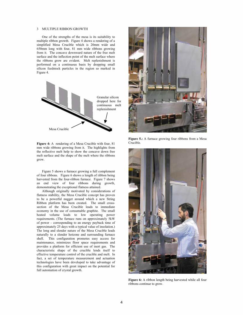
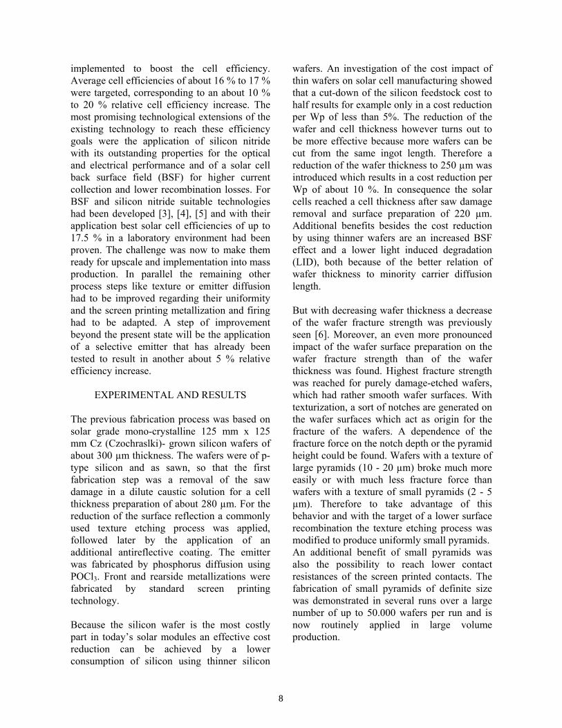
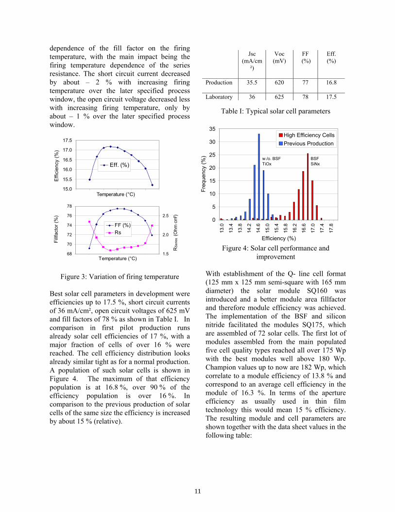
3 MULTIPLE RIBBON GROWTH One of the strengths of the mesa is its suitability to multiple ribbon growth. Figure 4 shows a rendering of a simplified Mesa Crucible which is 20mm wide and 650mm long with four, 81 mm wide ribbons growing from it. The concave downward nature of the free melt surface and the inflection point of the melt surface where the ribbons grow are evident. Melt replenishment is performed on a continuous basis by dropping small silicon feedstock particles in the region so marked in Figure 4. Figure 4: A rendering of a Mesa Crucible with four, 81 mm wide ribbons growing from it. The highlights from the reflective melt help to show the concave down free melt surface and the shape of the melt where the ribbons grow. Figure 5 shows a furnace growing a full complement of four ribbons. Figure 6 shows a length of ribbon being harvested from the four-ribbon furnace. Figure 7 shows an end view of four ribbons during growth, demonstrating the exceptional flatness attained. Although originally motivated by considerations of flatness stability, the Mesa Crucible concept has proven to be a powerful nugget around which a new String Ribbon platform has been created. The small cross-section of the Mesa Crucible leads to immediate economy in the use of consumable graphite. The small heated volume leads to low operating power requirements. (The furnace runs on approximately 5kW of power – corresponding to an energy payback time of approximately 25 days with a typical value of insolation.) The long and slender nature of the Mesa Crucible leads naturally to a slender hotzone and surrounding furnace shell. This configuration promotes easy access for maintenance, minimizes floor space requirements and provides a platform for efficient use of inert gas. The characteristic shape of the crucible lends itself to effective temperature control of the crucible and melt. In fact, a set of temperature measurement and actuation technologies have been developed to take advantage of this configuration with great impact on the potential for full automation of crystal growth.
Figure 5.: A furnace growing four ribbons from a Mesa Crucible.
Figure 6: A ribbon length being harvested while all four ribbons continue to grow.
Granular silicon dropped here forcontinuous meltreplenishment
Mesa Crucible
4

Figure 7: An edge-on view of four ribbons growing from a Mesa Crucible. Note the flatness. 4 CONCLUSION The Mesa Crucible contains molten silicon with no walls, thus promoting a concave down free melt surface, which in turn leads to inherent flatness stabilization for String Ribbon, as has been confirmed experimentally. The Mesa Crucible concept serves as the organizing nucleus for a new Platform for String Ribbon Growth which promises dramatic cost reductions together with the improved quality of the grown ribbon. A four-ribbon furnace has been developed and demonstrated using the mesa concept and a number of supporting technologies, especially in temperature measurement and actuation. Consumables such as argon, graphite, and electricity will be significantly reduced below the already low costs for String Ribbon. Capital costs on a per ribbon basis will be lowered and, given the degree of automation built into the system, labor costs are expected to be reduced. Further, the improved ribbon flatness will result in improvements in downstream yields.
5 REFERENCES [1] R.L.Wallace, et al, Multiple Ribbon Growth using the String Ribbon Method, 3rd WORLD CONFERENCE ON PHOTOVOLTAIC ENERGY CONVERSION, May 12-16, 2003, Osaka, Japan [2] Sachs, E.M., Ely, D., and Serdy, J, "Edge Stabilized Ribbon (ESR) Growth of Silicon for Low Cost Photovoltaics," J. Crystal Growth, 82, 117-121, 1987 6 ACKNOWLEDGMENTS The authors gratefully acknowledge funding for this work from The National Institute of Standards and Technology, Advanced Technology Program, contract # NANBOH3028.
5

Status of EWT Cells James Gee
Manuscript not available at time of printing.
6

HIGH EFFICIENCY SILICON SOLAR CELLS FOR PRODUCTION AT SHELL SOLAR
L. Mandrell*, N. Deyirmencian*, K.T. Holdermann* K.A. Münzer**, R.E. Schlosser **
* Shell Solar Industries, 4650 Adohr Lane, Camarillo, CA 93011, USA ** Shell Solar GmbH, Otto-Hahn-Ring 6, D- 81739 Munich, Germany
ABSTRACT: Advanced photovoltaic projects demand high efficient solar modules and solar cells at desirable low cost. The approach to reach this goal was an upgrade of the existing low cost technology with additional high efficiency generating process steps. For this purpose the developed fabrication processes for boron back surface field and silicon nitride were enabled for upscale and implementation into the existing fabrication process in large volume. Also the remaining process steps like texture or emitter diffusion were improved regarding their uniformity and the screen printing metallization and firing were adapted. The application of this advanced fabrication process enabled to produce solar cells of 17 % in large volume, with average efficiency of 16.5 % and the major fraction of cells over 16 %. Solar modules assembled of these cells of around 17 % efficiency reached a power output of 182 Wp, corresponding to an average calculated cell efficiency in the module of 16.3 % including the efficiency losses due to the module assembly.
INTRODUCTION
Silicon solar cells with highest efficiencies of up to 25 % have been demonstrated on small area solar cells in research [1]. Fundamental requirements for this achievement were wafers of high quality silicon material, a highly developed solar cell design including optimized light trapping, advanced emitter and front side surface passivation contacted by fine line metallization and a surface passivation with a local back surface field on the solar cell rear side. The technology includes photolithography for the surface texture and diffusion masks, evaporation and plating for the metallization and high quality surface passivation by silicon oxide or silicon nitride. In contrast, conventional state of the art mono-crystalline silicon solar cells with typical average cell efficiencies in production of about 15 % as an acceptable compromise for both power output and cost requirements were designed very simple consisting of textured surfaces, a simple pn-junction and screen printed contacts on the cell front and rear side, possibly completed with a single layer antireflection coating to increase the cell efficiency. A major difference to the highest efficiency solar cells is the application of lower
grade and lower cost silicon wafers, for example fabricated from Czochralski grown or multicrystalline cast silicon which can be specified very directly by the minority carrier diffusion length in the material. Applying high efficiency fabrication processes on lower grade silicon wafers best solar cell efficiencies of up to 22 % on monocrystalline Cz- wafers and of up to 19 % on multicrystalline wafers have been reached [2]. But in mass production only fabrication technologies, which are capable for production in large volume like random texture, maskless diffusion and screen printed metallization, are of interest. These restrictions result in additional solar cell efficiency decrease, for example by a less perfect light trapping, by a poorer emitter design and surface passivation, by higher rear side surface recombination and by higher shadowing of the metallization. But even insisting on low cost fabrication the photovoltaic evolution demands solar modules with higher power output and corresponding higher solar cell efficiencies. Therefore in order to increase today’s average Cz- silicon solar cell efficiencies in large volume production existing technologies had to be adapted and new additional technology steps had to be
7
implemented to boost the cell efficiency. Average cell efficiencies of about 16 % to 17 % were targeted, corresponding to an about 10 % to 20 % relative cell efficiency increase. The most promising technological extensions of the existing technology to reach these efficiency goals were the application of silicon nitride with its outstanding properties for the optical and electrical performance and of a solar cell back surface field (BSF) for higher current collection and lower recombination losses. For BSF and silicon nitride suitable technologies had been developed [3], [4], [5] and with their application best solar cell efficiencies of up to 17.5 % in a laboratory environment had been proven. The challenge was now to make them ready for upscale and implementation into mass production. In parallel the remaining other process steps like texture or emitter diffusion had to be improved regarding their uniformity and the screen printing metallization and firing had to be adapted. A step of improvement beyond the present state will be the application of a selective emitter that has already been tested to result in another about 5 % relative efficiency increase.
EXPERIMENTAL AND RESULTS
The previous fabrication process was based on solar grade mono-crystalline 125 mm x 125 mm Cz (Czochraslki)- grown silicon wafers of about 300 µm thickness. The wafers were of p-type silicon and as sawn, so that the first fabrication step was a removal of the saw damage in a dilute caustic solution for a cell thickness preparation of about 280 µm. For the reduction of the surface reflection a commonly used texture etching process was applied, followed later by the application of an additional antireflective coating. The emitter was fabricated by phosphorus diffusion using POCl3. Front and rearside metallizations were fabricated by standard screen printing technology. Because the silicon wafer is the most costly part in today’s solar modules an effective cost reduction can be achieved by a lower consumption of silicon using thinner silicon
wafers. An investigation of the cost impact of thin wafers on solar cell manufacturing showed that a cut-down of the silicon feedstock cost to half results for example only in a cost reduction per Wp of less than 5%. The reduction of the wafer and cell thickness however turns out to be more effective because more wafers can be cut from the same ingot length. Therefore a reduction of the wafer thickness to 250 µm was introduced which results in a cost reduction per Wp of about 10 %. In consequence the solar cells reached a cell thickness after saw damage removal and surface preparation of 220 µm. Additional benefits besides the cost reduction by using thinner wafers are an increased BSF effect and a lower light induced degradation (LID), both because of the better relation of wafer thickness to minority carrier diffusion length. But with decreasing wafer thickness a decrease of the wafer fracture strength was previously seen [6]. Moreover, an even more pronounced impact of the wafer surface preparation on the wafer fracture strength than of the wafer thickness was found. Highest fracture strength was reached for purely damage-etched wafers, which had rather smooth wafer surfaces. With texturization, a sort of notches are generated on the wafer surfaces which act as origin for the fracture of the wafers. A dependence of the fracture force on the notch depth or the pyramid height could be found. Wafers with a texture of large pyramids (10 - 20 µm) broke much more easily or with much less fracture force than wafers with a texture of small pyramids (2 - 5 µm). Therefore to take advantage of this behavior and with the target of a lower surface recombination the texture etching process was modified to produce uniformly small pyramids. An additional benefit of small pyramids was also the possibility to reach lower contact resistances of the screen printed contacts. The fabrication of small pyramids of definite size was demonstrated in several runs over a large number of up to 50.000 wafers per run and is now routinely applied in large volume production.
8

But using conventional cell manufacturing technology the electrical performance of thin cells decreases as described in [6] for solar cells with and without a BSF for cell thickness in the range of 450 µm to 100 µm. Because the decrease in efficiency with decreasing wafer thickness is mainly the result of the carrier recombination at the solar cell back surface, the losses can be reduced by the application of an additional electrical field at the back surface (BSF). This field keeps the minority carriers away from the back surface and thus reduces the back surface recombination. Therefore, a process for the application of a back-surface-field (BSF) was developed which is now implemented into production. The effect of the BSF can be recognized in the spectral response respective the quantum efficiency of the solar cell as shown in Figure1. The BSF reduces the recombination induced minority carrier losses at the rear surface and therefore increases the red response of the cells. A similar effect is also reached by higher quality silicon wafer material, which implies higher diffusion lengths of the minority carrier diffusion lengths. Therefore the evaluation of the spectral response in the mid and red range delivers a result for the combination of both the diffusion length in the silicon and the recombination on the rear surface. A much more sensitive method for the evaluation of the rear side recombination velocity is the investigation of the spectral response with illumination of the solar cell from the rear side [7]. Similar to many commercial crystalline silicon solar cells, a gridded contact on the back surface to reduce the consumption of the expensive silver metallization paste was used for the rear contact of solar cells with a boron BSF, which is optically transparent without metallization. Therefore by illumination light can penetrate the solar cell from the rear side and spectral response measurements with illumination of the rear side can be performed. This rear surface spectral response is very sensitive to bulk diffusion length and the back surface recombination and in many cases can provide
information on these parameters that is not obtainable from the analysis of front surface spectral data. Similar to the evaluation of the spectral response from the solar cell front side the rear side spectral response can be evaluated to provide information about the minority carrier diffusion length L and the rear surface recombination velocity S. After determination of L by front side spectral response measurements, S can be calculated using the rear side spectral response.
Figure 1: Internal quantum efficiencies of cells with and without BSF measured with front or
rear illumination Both methods, the spectral response measured with illumination from the front side or from the rear side, were applied to typical high efficiency BSF cells and the resulting internal quantum efficiency curves (IQE) were compared with calculated (PC1D) internal quantum responses dependent on diffusion length and rear surface recombination velocity. With an evaluated diffusion length from the front side spectral response of about 200 µm a rear side recombination of the applied BSF of about 800 cm/sec was derived. The low surface recombination velocity (~ 800 cm/sec) on the solar cell rear side due to an entire boron back surface field (BSF) increased the short circuit currents for all wafer resistivities by about 2.5 mA/cm² and in particular preserved the open circuit voltages even for higher resistivity wafers.
9

The boron BSF also allows semi-transparent back surfaces for bifacial cell applications. Dependent on the application an efficiency increase of the bifacial illuminated cells is possible. For the cell frontside usually thermally diffused phosphorus profiles are applied with a high surface dopand concentration to reduce the contact resistance. Advanced emitters for higher current collection with a high blue response however demand a lower pn-junction penetration depth or lower doping concentrations. But when using silver contacts highly doped silicon below the contacts is necessary. These implications would require a selectively doped emitter with low concentration doping between the metal contacts and high doping below the metal contacts is required. But for process simplicity the emitter was only adapted to a medium dopand concentration sufficient regarding contacting issues and with low enough penetration depth respective high blue responsivity of the solar cells. The application of this emitter type resulted in a blue response of about 70 % in the blue wavelength range below 500 nm. Corresponding to the doping profile this emitter could be passivated by oxide or silicon nitride. Regarding better matching with module requirements silicon nitride was applied, which combines both the properties of passivation and very effective antireflective coating. In Figure 2 the reflection of different coated silicon surfaces are shown. The application of a surface texture decreases the reflection almost independent of the wavelength over the whole wavelength range of 300 nm to 1100 nm by about 25 % compared to a polished silicon surface. Applying a thick silicon oxide antireflective (AR) layer of about 100 nm the reflection was reduced by another about 7 %, with decreasing effect in the blue wavelength range. The combination of silicon oxide and titanium oxide, which is used because of the passivation effect of the silicon oxide as the
Figure2: Spectral reflectance of different surface coatings
first layer on the silicon and the antireflection effect of the titanium oxide with its favorable refractive index, reduced the reflection by about 9 %, compared to the pure textured surface. But for the production silicon nitride was selected, which combines both the passivation of the silicon surface and the AR- coating in one layer with a suitable refractive index of about 2. An additional reduction of the reflection of about 3 % over the whole wavelength range compared to titanium oxide and a further reflection reduction in the blue wavelength range from 400 nm to 500 nm was found, which is important especially when using high blue responsible emitters. In total with the application of silicon nitride on textured silicon the reflection could be minimized below 3 %. According to the silicon nitride coating the metallization had to be adapted regarding low contact resistance. Screen printing metallization pastes have been selected for the front and rear side, which are suitable for contacting through the silicon nitride layer. In accordance with the doping profiles and the silicon nitride the optimum firing conditions had to be found for the established co-firing of the front and rear side pastes. Figure 3 shows the dependence of the solar cell parameters on the variation of the firing conditions. For the efficiency a maximum was found with a sufficient wide firing temperature window to reach solar cell efficiencies of up to 17 %. This efficiency dependence was mainly determined by the
0
10
20
30
40
50
60
70
80
100 300 500 700 900 1100 1300Wavelength (nm)
PolishedTextureTexture, SiOx 100 nmTexture, SiOx-TiOxTexture, SiNx
10
dependence of the fill factor on the firing temperature, with the main impact being the firing temperature dependence of the series resistance. The short circuit current decreased by about – 2 % with increasing firing temperature over the later specified process window, the open circuit voltage decreased less with increasing firing temperature, only by about – 1 % over the later specified process window.
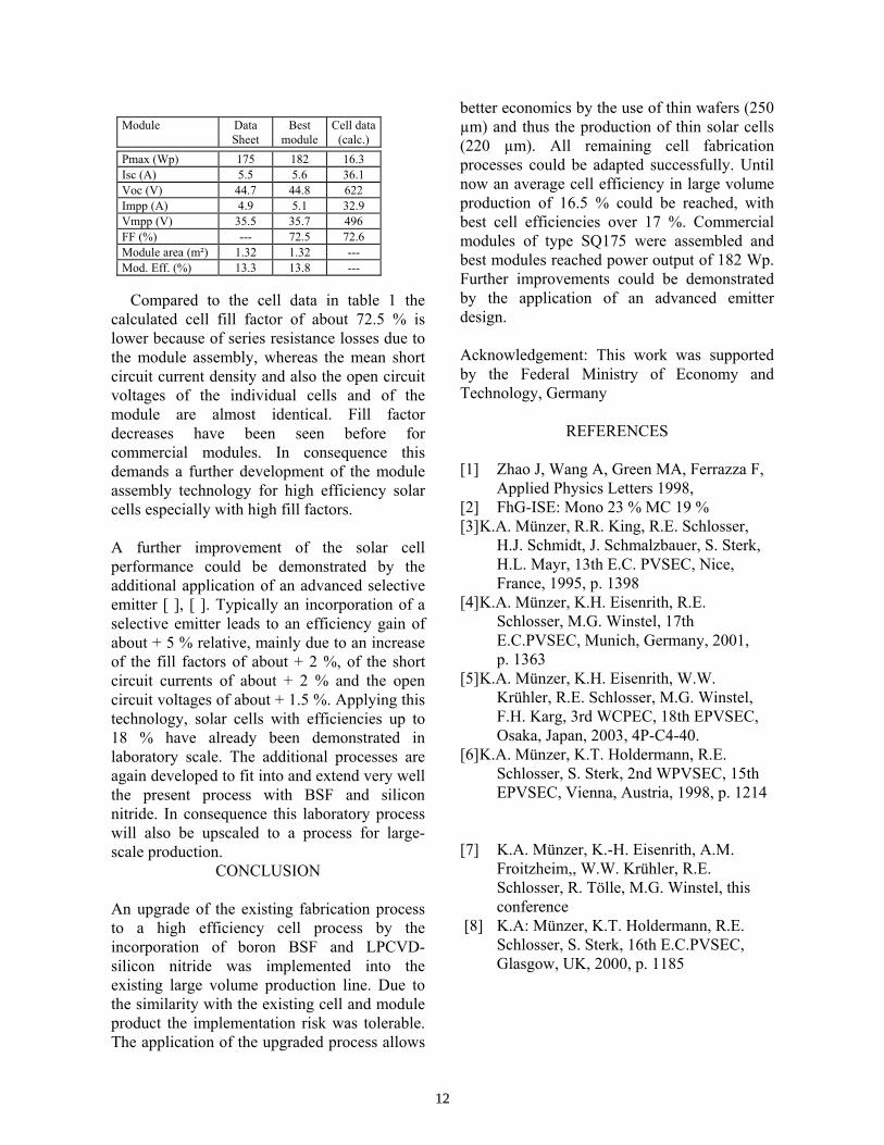
Figure 3: Variation of firing temperature Best solar cell parameters in development were efficiencies up to 17.5 %, short circuit currents of 36 mA/cm², open circuit voltages of 625 mV and fill factors of 78 % as shown in Table I. In comparison in first pilot production runs already solar cell efficiencies of 17 %, with a major fraction of cells of over 16 % were reached. The cell efficiency distribution looks already similar tight as for a normal production. A population of such solar cells is shown in Figure 4. The maximum of that efficiency population is at 16.8 %, over 90 % of the efficiency population is over 16 %. In comparison to the previous production of solar cells of the same size the efficiency is increased by about 15 % (relative).
Jsc
(mA/cm²)
Voc (mV)
FF (%)
Eff. (%)
Production 35.5 620 77 16.8 Laboratory 36 625 78 17.5
Table I: Typical solar cell parameters
Figure 4: Solar cell performance and improvement
With establishment of the Q- line cell format (125 mm x 125 mm semi-square with 165 mm diameter) the solar module SQ160 was introduced and a better module area fillfactor and therefore module efficiency was achieved. The implementation of the BSF and silicon nitride facilitated the modules SQ175, which are assembled of 72 solar cells. The first lot of modules assembled from the main populated five cell quality types reached all over 175 Wp with the best modules well above 180 Wp. Champion values up to now are 182 Wp, which correlate to a module efficiency of 13.8 % and correspond to an average cell efficiency in the module of 16.3 %. In terms of the aperture efficiency as usually used in thin film technology this would mean 15 % efficiency. The resulting module and cell parameters are shown together with the data sheet values in the following table:
68
70
72
74
76
78
780 800 820 840 860 880 900Temperature (°C)
Fillf
acto
r (%
)
1.5
2.0
2.5
RS
erie
s (O
hm c
m²)
FF (%)Rs
15.0
15.5
16.0
16.5
17.0
17.5
780 800 820 840 860 880 900Temperature (°C)
Effi
cien
cy (%
)
Eff. (%)
0
5
10
15
20
25
30
35
13.0
13.4
13.8
14.2
14.6
15.0
15.4
15.8
16.2
16.6
17.0
17.4
17.8
Efficiency (%)
Freq
uenc
y (%
)
High Efficiency CellsPrevious Production
w./o. BSFTiOx
BSFSiNx
11
Module Data
Sheet Best
module Cell data
(calc.)
Pmax (Wp) 175 182 16.3 Isc (A) 5.5 5.6 36.1 Voc (V) 44.7 44.8 622 Impp (A) 4.9 5.1 32.9 Vmpp (V) 35.5 35.7 496 FF (%) --- 72.5 72.6 Module area (m²) 1.32 1.32 --- Mod. Eff. (%) 13.3 13.8 ---
Compared to the cell data in table 1 the
calculated cell fill factor of about 72.5 % is lower because of series resistance losses due to the module assembly, whereas the mean short circuit current density and also the open circuit voltages of the individual cells and of the module are almost identical. Fill factor decreases have been seen before for commercial modules. In consequence this demands a further development of the module assembly technology for high efficiency solar cells especially with high fill factors.
A further improvement of the solar cell performance could be demonstrated by the additional application of an advanced selective emitter [ ], [ ]. Typically an incorporation of a selective emitter leads to an efficiency gain of about + 5 % relative, mainly due to an increase of the fill factors of about + 2 %, of the short circuit currents of about + 2 % and the open circuit voltages of about + 1.5 %. Applying this technology, solar cells with efficiencies up to 18 % have already been demonstrated in laboratory scale. The additional processes are again developed to fit into and extend very well the present process with BSF and silicon nitride. In consequence this laboratory process will also be upscaled to a process for large-scale production.
CONCLUSION An upgrade of the existing fabrication process to a high efficiency cell process by the incorporation of boron BSF and LPCVD- silicon nitride was implemented into the existing large volume production line. Due to the similarity with the existing cell and module product the implementation risk was tolerable. The application of the upgraded process allows
better economics by the use of thin wafers (250 µm) and thus the production of thin solar cells (220 µm). All remaining cell fabrication processes could be adapted successfully. Until now an average cell efficiency in large volume production of 16.5 % could be reached, with best cell efficiencies over 17 %. Commercial modules of type SQ175 were assembled and best modules reached power output of 182 Wp. Further improvements could be demonstrated by the application of an advanced emitter design. Acknowledgement: This work was supported by the Federal Ministry of Economy and Technology, Germany
REFERENCES
[1] Zhao J, Wang A, Green MA, Ferrazza F, Applied Physics Letters 1998, [2] FhG-ISE: Mono 23 % MC 19 % [3] K.A. Münzer, R.R. King, R.E. Schlosser, H.J. Schmidt, J. Schmalzbauer, S. Sterk, H.L. Mayr, 13th E.C. PVSEC, Nice, France, 1995, p. 1398 [4] K.A. Münzer, K.H. Eisenrith, R.E. Schlosser, M.G. Winstel, 17th E.C.PVSEC, Munich, Germany, 2001, p. 1363 [5] K.A. Münzer, K.H. Eisenrith, W.W. Krühler, R.E. Schlosser, M.G. Winstel, F.H. Karg, 3rd WCPEC, 18th EPVSEC, Osaka, Japan, 2003, 4P-C4-40. [6] K.A. Münzer, K.T. Holdermann, R.E. Schlosser, S. Sterk, 2nd WPVSEC, 15th EPVSEC, Vienna, Austria, 1998, p. 1214 [7] K.A. Münzer, K.-H. Eisenrith, A.M. Froitzheim,, W.W. Krühler, R.E. Schlosser, R. Tölle, M.G. Winstel, this conference [8] K.A: Münzer, K.T. Holdermann, R.E. Schlosser, S. Sterk, 16th E.C.PVSEC, Glasgow, UK, 2000, p. 1185
12

Monitoring thermo-elastic residual stress in mc-Si wafers with vibration
S. R. Best, D. P. Hess, A. Belyaev, S. Ostapenko and J. P. Kalejs*
University of South Florida, Tampa, FL RWE Schott Solar Inc, Billerica, MA*
Abstract. This paper presents audible vibratory mode data obtained by mechanically exciting acoustic modes in multicrystalline silicon wafers with various levels and distributions of residual stress. The vibratory data is found to correlate with residual stress optical polariscopy measurements. The data is fit with a quadratic model with a correlation coefficient of 0.8. The results reveal a dependence of wafer audible mode frequencies on residual stress level that may be useful for solar cell mechanical quality control and breakage inspection. Introduction In the production of multi-crystalline silicon (mc-Si) ribbons and tubes, applied thermo-elastic stress may exceed levels of 100 MPa. The residual stress level and its spatial distribution in wafers cut from the ribbons depend on growth speed, thickness, and temperatue gradients present during growth [1]. Stress deteriorates mechanical quality of solar cells through dislocations generated during crystal growth. Additional stress may arise in wafers during processing into solar cells, e.g., from bulk defect precipitates, thin film deposition such as a Si3N4 anti-reflecting coating, Al-backside contact firing, and wafer handling. When augmented by stresses arising during cell processing, the high wafer residual stress enhances wafer breakage and yield reduction in solar cell production lines. In addition, this stress promotes various types of defect reactions, such as precipitation of residual impurities at dislocations, which deteriorate the electronic quality of the solar-grade mc-Si wafers [2].
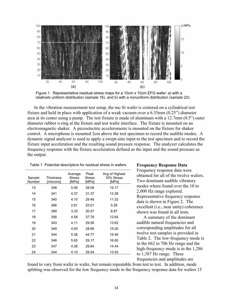
There exists a need in the solar cell industry for methods of non-contact and non-destructive in-line and off-line monitoring of wafer residual stresses in as-grown as well as processed mc-Si wafers. In this paper, audible vibratory modes of mc-Si wafers arising from mechanical excitations of the wafer are used to diagnose residual stress. The results show promise for a fast and reliable metrological tool for in-line diagnostics of residual stress in wafers which may be correlated to as-grown and process-induced defects. Samples and Measurement A set of 10cm x 10cm as-grown mc-Si wafers produced by the Edge-defined Film-fed Growth (EFG) method [3] with a nominal 340 micron thickness was used in this study. Following SAM inspection, the wafers were measured with scanning infrared polariscopy to assess the level and distribution of in-plane stress using a method described elsewhere [4]. Stress maps of the twelve test wafers were obtained from this infrared polariscopy. Representative stress maps are presented in Figure 1. Each of the stress maps uses a grid of 100x100 data points to cover the 10 cm square wafer.
Potential single number descriptors have been identified to quantify the stress maps. These include average stress, peak stress, average of lowest ten percent stress, average of highest ten percent stress, and average of highest five percent stress. Table 1 summarizes the computed values of some of these descriptors for the twelve test wafers.
13
In the vibration measurement test setup, the mc-Si wafer is centered on a cylindrical test
fixture and held in place with application of a weak vacuum over a 6.35mm (0.25”) diameter area at its center using a pump. The test fixture is made of aluminum with a 12.7mm (0.5”) outer diameter rubber o-ring at the fixture and test wafer interface. The fixture is mounted on an electromagnetic shaker. A piezoelectric accelerometer is mounted on the fixture for shaker control. A microphone is mounted 2cm above the test specimen to record the audible modes. A dynamic signal analyzer is used to apply a swept-sine input to the test specimen and to record the fixture input acceleration and the resulting sound pressure response. The analyzer calculates the frequency response with the fixture acceleration defined as the input and the sound pressure as the output.
Frequency Response Data Frequency response data were obtained for all of the twelve wafers. Two dominant audible vibratory modes where found over the 10 to 2,000 Hz range explored. Representative frequency response data is shown in Figure 2. The excellent (i.e., near unity) coherence shown was found in all tests.
A summary of the dominant audible natural frequencies and corresponding amplitudes for all twelve test samples is provided in Table 2. The low-frequency mode is in the 662 to 706 Hz range and the high-frequency mode is in the 1,286 to 1,387 Hz range. These frequencies and amplitudes are
found to vary from wafer to wafer, but remain repeatable from test to test. In addition, mode splitting was observed for the low frequency mode in the frequency response data for wafers 15
Sample Number
Thickness [microns]
Average Stress [MPa]
Peak Stress [MPa]
Avg of Highest 10% Stress
[MPa]
13 348 5.06 28.58 15.17
14 341 4.37 31.37 13.38
15 340 4.10 29.46 11.32
16 366 2.81 25.01 5.28
17 369 3.33 30.57 8.87
18 356 4.58 37.78 12.64
19 343 4.11 29.56 13.62
20 349 4.93 28.66 15.00
21 344 5.38 44.77 15.46
22 346 5.65 29.17 16.60
23 347 4.36 29.84 14.44
24 344 4.10 29.54 13.93
(a) (b)
MPa
Figure 1 Representative residual stress maps for a 10cm x 10cm EFG wafer: a) with a relatively uniform distribution (sample 16), and b) with a nonuniform distribution (sample 22).
Table 1 Potential descriptors for residual stress in wafers
(a) (b)
14
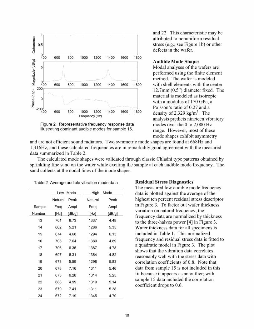
and 22. This characteristic may be attributed to nonuniform residual stress (e.g., see Figure 1b) or other defects in the wafer. Audible Mode Shapes Modal analyses of the wafers are performed using the finite element method. The wafer is modeled with shell elements with the center 12.7mm (0.5”) diameter fixed. The material is modeled as isotropic with a modulus of 170 GPa, a Poisson’s ratio of 0.27 and a density of 2,329 kg/m3. The analysis predicts nineteen vibratory modes over the 0 to 2,000 Hz range. However, most of these mode shapes exhibit asymmetry
and are not efficient sound radiators. Two symmetric mode shapes are found at 668Hz and 1,316Hz, and these calculated frequencies are in remarkably good agreement with the measured data summarized in Table 2.
The calculated mode shapes were validated through classic Chladni type patterns obtained by sprinkling fine sand on the wafer while exciting the sample at each audible mode frequency. The sand collects at the nodal lines of the mode shapes.
Residual Stress Diagnostics The measured low audible mode frequency data is plotted against the average of the highest ten percent residual stress descriptor in Figure 3. To factor out wafer thickness variation on natural frequency, the frequency data are normalized by thickness to the three-halves power [4] in Figure 3. Wafer thickness data for all specimens is included in Table 1. This normalized frequency and residual stress data is fitted to a quadratic model in Figure 3. The plot shows that the vibration data correlates reasonably well with the stress data with correlation coefficients of 0.8. Note that data from sample 15 is not included in this fit because it appears as an outlier; with sample 15 data included the correlation coefficient drops to 0.6.
Low Mode High Mode
Natural Peak Natural Peak
Sample Freq Ampl Freq Ampl
Number [Hz] [dB/g] [Hz] [dB/g]
13 701 6.73 1337 4.48
14 662 5.21 1286 5.35
15 674 4.68 1294 6.13
16 703 7.64 1380 4.89
17 706 6.35 1387 4.78
18 697 6.31 1364 4.82
19 673 5.59 1298 5.83
20 678 7.16 1311 5.46
21 673 6.28 1314 5.25
22 688 4.99 1319 5.14
23 679 7.41 1311 5.38
24 672 7.19 1345 4.70
400 600 800 1000 1200 1400 1600 18000
0.5
1C
oher
ence
400 600 800 1000 1200 1400 1600 18000
5
Mag
nitu
de (d
B/g
)
400 600 800 1000 1200 1400 1600 1800-200
0
200
Pha
se (d
eg)
Frequency (Hz)
Figure 2 Representative frequency response data illustrating dominant audible modes for sample 16.
Table 2 Average audible vibration mode data
15

Conclusions Audible vibratory mode data from a set of EFG mc-Si wafers with various levels and distributions of residual stress has been presented. The audible modes have been found to exhibit symmetry compared to non-audible vibratory modes. Mode splitting has been found in frequency response measurements of wafers with nonuniform residual stress distributions. Analysis of this vibratory data and the wafer residual stress measurements has shown reasonably good correlation for a quadratic model. The audible natural frequencies of the wafers have been found to increase with increasing stress. Acknowledgment. This work was supported in part by DOE/NREL subcontract AAT-2-31605-06. References 1. Y. Kwon, S. Danyluk, L. Bucciarelli and J. P. Kalejs 1987 J. Crystal Growth 82, 221-227.
Residual stress measurement in silicon sheet by Shadow Moire interferometry. 2. S. Ostapenko, I Tarasov, J. P. Kalejs, C. Haessler and E. U. Reisner 2000 Semicond. Sci.
Technol. 15, 840-848. Defect monitoring using scanning photoluuminescence spectroscopy in mc-Si wafers.
3. J. P. Kalejs 2004 Diffusion and Defect Data Part B (Solid State Phenomena) 95-96 159-174. Silicon ribbons for solar cells.
4. R. D. Blevins 2001 Formulas for Natural Frequency and Mode Shape. Florida: Krieger Publishing.
16
17
18
24
13
14
19
20
21
22
23
y = 3E-05x2 - 3E-05x + 0.099R2 = 0.8
0.099
0.100
0.101
0.102
0.103
0.104
0.105
0.106
0.107
0.108
0.109
4.00 6.00 8.00 10.00 12.00 14.00 16.00 18.00
Average of the Highest 10% Residual Stress (MPa)
Nor
mal
ized
Nat
ural
Fre
quen
cy, f
/h3/
2 (Hz
/ µm
3/2 )
Figure 3 Quadratic correlation of normalized low audible mode frequency with residual stress.
16

TRANSITION METALS IN MULTICRYSTALLINE SOLAR CELLS: Understanding the nature, origins, and impacts of metal contamination
in multicrystalline Si and minimizing its impact on solar cell performance
T. Buonassisi, A. A. Istratov, and E. R. Weber University of California, Berkeley, CA 94720
I. INTRODUCTION AND MOTIVATION Metals, which are known to form recombination-active point defects and precipitates in silicon, can substantially decrease material performance. For example, just 2×1012 cm-3 of intersti-tial iron or 2×1013 cm-3 of iron-boron pairs can reduce the minority carrier diffusion length to 50 µm (τ ~ 1 µs), which can lead to substantial decreases in both Jsc and Voc of traditional photo-voltaic devices. The results of recent neutron activation analysis (NAA) studies to determine the total metal content in multicrystalline (mc)-Si materials were thus rather surprising, as the iron content in these materials was revealed to be as high as 1014 to 1016 cm-3, the concentration of Ni and Cr was 1013 to 1015 cm-3, and the concentrations of Co and Mo between 1012 and 1013 cm-3.1,2 Were all these metal atoms as recombination-active as interstitial or substitutional metal species, the material performance of such devices would render them unusable. If metals are present in such high quantities yet mc-Si solar cells manage to obtain rea-sonable operating efficiencies, then the key to understanding the effect of metals on device per-formance must lie in characteristics other than the total metal concentration, i.e. their nature, chemical state, and distribution. Electrical techniques such as deep level transient spectroscopy (DLTS) typically show a very small density of electrically-active defects, indicating that metals are not in the interstitial state, but most likely precipitated. Additionally, if 1015-16 cm-3 of iron were introduced directly from the melt via segregation into single-crystalline regions, then given the known segregation coefficient of iron, over 1020 Fe cm-3 (0.1 atomic %) should be dissolved in the melt. Such high metal concentrations are known to affect the stability of the solidification front, leading to smaller grain sizes and greater densi-ties of structural defects. Because this does not occur, the dominant pathways for the introduction of iron into mc-Si material must occur via mechanisms other than segregation from the melt into single-crystalline regions. To investigate the origins and characteristics of metal contamination in mc-Si, we have employed a variety of synchrotron-based analytical microprobe techniques. X-ray fluorescence microscopy (µ-XRF) reveals the elemental nature and location of nanometer-sized metal-rich particles embedded within the silicon matrix; detection limits have been steadily improving and now, within 1 second accumulation time, a single FeSi2 particle close to the surface with a radius of 16±3 nm can be detected. X-ray absorption microspectroscopy (µ-XAS) measures the absorp-tion spectrum of an impurity precipitate, which is a unique signature of its chemical phase. The µ-XAS technique is thus capable of determining the chemical state of metal-rich clusters. Lastly, the X-ray beam induced current (XBIC) technique is capable of mapping the recombination-activity of metal clusters, using the incoming X-rays as the excitation source in a manner analo-gous to laser beam induced current (LBIC). All three techniques can be performed at the same beamline without removing the sample from the sample stage, thus an accurate correlation can be traced between recombination activity, metallic impurity clusters, and their chemical states. More details about these techniques can be found in Refs. 3,4. In addition, with these synchro-tron-based microprobe techniques it is possible to investigate defective regions identified via
17

macroscopic device measurement techniques such as lock-in thermography, by using the XBIC/LBIC correlation to identify the same region of the sample.5 II. NATURE OF METAL CONTAMINATION IN MC-SI The analysis of a variety of mc-Si materials, including those grown by cast, sheet, and ribbon techniques, has revealed the following trends:
(1) Many smaller (• 1 µm diameter, often as small as 50-60 nm in diameter) metal-silicide particles can be detected by µ-XRF in most as-grown mc-Si materials. These particles, because of their metal-silicide phase, are likely to have formed via precipitation of dissolved metal atoms during the crystal growth process, including cooling the crystal to room temperature. Numerous copper, iron, and nickel silicide particles were analyzed over the course of several studies.
(2) The majority of these smaller particles are observed at either structural defects (e.g. grain boundaries), or at intragranular defect clusters (also believed to be associated with struc-tural defects). Despite their small size, these particles typically have a high spatial density, yield-ing equivalent bulk metal concentrations between 1014 and 1015 cm-3.
(3) Fewer large (• 1 µm) metal-rich particles are also observed. These particles are often oxidized and composed of multiple impurity species (e.g. Fe, Cr, Ni, Mn, Ca). These particles, because of their large size, chemical state, and elemental composition, are believed to be inclu-sions of foreign particles. Such particles may originate from the feedstock, crucible linings, growth substrate, etc. Once in the melt, such oxidized particles are likely to survive for an ex-tended period of time because of their high melting point, but liquid silicon invariably attacks these particles, reducing their size until they can be incorporated into the advancing solidification front. The metals dissolved from such particles may enter the melt and precipitate in other areas of the ingot, resulting in the more distributed metal silicide nanoparticles. III. INTRODUCTION OF METALS INTO MC-SI Our results presented in the previous section discuss experimental results which indicate that metals can reach the silicon melt by dissolving from a foreign source (e.g. the crucible lin-ings, particles in the feedstock, growth surfaces, etc.). The question remains, however, as to how the dissolved metals are introduced into the mc-Si crystal in such high concentrations as revealed by our µ-XRF and NAA studies. With crystal growth speeds V[cm/min] of directional solidifica-tion techniques similar to or even slower than high-purity Czochralski or Float Zone methods, the high concentration of metals contained in metal silicide particles cannot simply be introduced via segregation of metals into single-crystalline regions and their subsequent precipitation. There is no doubt that large oxidized particles which did not get fully dissolved in the melt and got trapped in the crystal by the advancing solidification front may account for a con-siderable fraction of the total metal content of the analyzed wafers. However, their density was too low to explain the high metal content of the mc-Si wafers (typically we observed a single such particle per five to ten analyzed samples). Our experimental results indicate that the segregation of metals to grain boundaries in mc-Si is another mechanism that may contribute to the introduction of a high metal content of mc-Si materials. We have recently observed (c.f. Istratov et al., these proceedings) that the equi-librium concentration of metals in a layer of polycrystalline silicon established within the tem-perature range of 1200°C to 1020°C exceeds its equilibrium solubility in single crystalline sili-con by a factor from 2.2 to 16. The enhancement factor appears to depend on the crystalline structure of the polysilicon layer and on the temperature. This phenomenon of impurity segrega-
18
tion to polycrystalline silicon was also observed for other impurity species such as copper, arse-nic, phosphorus, and boron. The physics of this interaction is believed due to differences in con-figurational entropy of metal atoms in a perfect and in a distorted silicon lattice6, and also due to formation of covalent bonding between interstitial metals and reconstructed and dangling silicon bonds in the cores of grain boundaries.7 These factors can substantially increase the apparent metal solubility in poly-Si and mc-Si. The final result is that the total amount of metals that can be trapped in multicrystalline and polycrystalline silicon during growth can be much higher than in single-crystalline silicon under comparable growth conditions. In other words, the effective distribution coefficient for metals between the silicon melt and mc-Si is much closer to 1 than would be the case for single-crystalline silicon. Estimates based on the assumption that segregated metals cover grain bounda-ries with the density of 1 atomic percent (see Istratov et al., these proceedings) reveal that up to 1014 Fe can be incorporated into mc-Si in this manner, approaching values detected in neutron activation analysis. Since according to the existing experimental data for Cu and Fe, the solubil-ity of metals in distorted silicon lattice areas at grain boundaries appears to decrease less rapidly with decreasing temperature than in single-crystalline silicon, interstitially-dissolved metals within the grains are likely to diffuse to these structural defects. Eventually, with the concentra-tion reaching critical levels, precipitation is likely to occur, and a driving force develops for more metals to precipitate at the grain boundaries via the relaxation mechanism. In certain as-grown cast mc-Si materials, µ-XRF has detected ~1014 Fe cm-3 distributed in iron-silicide particles at grain boundaries, each approximately 30 nm in diameter and separated by ~8-9 µm. In addition to grain boundary segregation of metals, other mechanisms specific to the accumulation of met-als at the liquid-solid interface in the silicon melt may also be involved with the formation of these metal clusters, and future work is required to fully understand these mechanisms at play. Hence, grain boundaries and structural defects are very efficient gettering sites which trap metals via both relaxation and segregation mechanisms, and are in constant competition for met-als both during crystal growth and during every intentional gettering sequence. IV. EFFECT OF METAL DISTRIBUTION ON DEVICE PERFORMANCE The effect of metal distribution in mc-Si was monitored by a combination of µ-XRF/XBIC on a variety of samples, including model defect structures and actual mc-Si solar cell material. Firstly, it is well known that metals can form recombination-active defect centers in sili-con. To begin to understand the effect of metal distribution on device performance, let us con-sider a sample with 1014 cm-3 iron-boron pairs (Fei-Bs) or interstitial iron (Fei). The minority car-rier diffusion length in such a sample would be 20 µm or 10 µm, respectively.8 Now, let us as-sume these iron atoms are now allowed to diffuse towards one another and form precipitates of iron-silicide. If we approximate the new minority carrier diffusion length as the distance between neighboring iron silicide clusters, then it is easy to calculate that if the same amount of iron forms precipitates with diameters of 60 nm form, then the diffusion length would be ~30 µm, if precipitates with diameters 350 nm form, the average diffusion length would be ~180 µm, etc. One can quickly see the pattern: with increasing average precipitate size (and decreasing density of precipitates), the minority carrier diffusion length increases. It can thus be concluded that it is the distribution of metals, and not their total bulk concentration, that affects device per-formance in mc-Si. We illustrate this principle with a study of how the distribution of metals can change in a mc-Si sample due to good and bad processing sequences. In a study performed in collaboration with C. Ballif, S. Peters, and R. Schindler of Fraunhofer Institute for Solar Energy Systems
19

(Freiburg/Gelsenkirchen, Germany), three cast mc-Si sister wafers (i.e. wafers cut from nearly the same region of the cast ingot, such that they have nearly identical crystal structure) were se-lected from the bottom of the ingot. In as-grown material, Fe-silicide precipitates measuring ~30 nm in radius were detected by µ-XRF at the grain boundaries in the material. The two sister wa-fers were then processed at different temperatures, and the equivalent grain boundaries in the sis-ter wafers were scanned with µ-XRF to see the impact of processing on the average size of the iron-silicide particles. The emitter of one sister wafer was diffused via a rapid thermal anneal (RTA, 100°C/s) at 1000°C for 20 seconds, while the other was subject to an RTA at 860°C for 120 seconds. µ-XRF mapping of the grain boundary in the high-temperature (1000°C) sample revealed that the Fe-rich clusters along the grain boundaries had been reduced to ~23 nm in ra-dius, i.e. a ~50% reduction of the total Fe content. However, in the sample processed at 860°C, large (i.e. radius ~30 nm) iron silicide precipitates were still evident. One can conclude that the high temperature anneal was successful in dissolving some of the iron from the iron silicide pre-cipitates at the grain boundaries, while the lower-temperature anneal was not. This is shown in the µ-XRF maps of Fig. 1 (a-c). The effects of the different iron distributions in these samples are shown by comparing Figs. 1 (d-f), the XBIC maps of these samples. In the as-grown sample, where iron is concen-trated in large clusters at the grain boundaries, denuded zones are evident surrounding the grain boundaries, and relatively low recombination activity is evident within the grains, with the ex-ceptions of some isolated intragranular defects. The same can generally be said for the sample processed at lower temperatures (860°C), wherein large iron silicide clusters were also detected by µ-XRF/XAS, indicating little dissolution of these clusters during the anneal. However, for the sample processed at high temperatures (1000°C), wherein the iron content at the grain bounda-ries decreased significantly, the intragranular regions demonstrate a dramatically increased re-combination activity. This is believed to be due to the dissolved iron, which diffused into the grains from iron-silicide precipitates located at the grain boundaries and intragranular locations. During the fast cool (100°C/s), the dissolved iron quickly supersaturated and could not diffuse to the gettering layers, and instead formed interstitial defects or smaller silicide clusters. The result of this delocalized precipitation of iron was a solar cell that has an efficiency 20% (rel.) lower than the cell processed at lower temperatures (860°C). The effect of metal distribution on device performance is also seen within different re-gions of the same samples. Regions containing an increased density of metal-rich clusters consis-tently perform worse than regions containing a lower density of such clusters. This effect is illus-trated in Fig. 2 (from Ref. 3), which shows the XBIC map of a multicrystalline float zone9 sam-ple contaminated with copper during crystal growth. In regions where there the spatial density of Cu-rich particles is lower, the diffusion length is increased accordingly. The same effect can be observed for mc-Si materials (see Buonassisi et al., this conference). Within the following sections, an overview is provided of our studies aiming to reduce the density of recombination-active metal-related defect clusters in mc-Si. V. STRATEGIES TO REDUCE THE DENSITY OF RECOMBINATION-ACTIVE METAL-RELATED DEFECTS IN MC-SI To minimize the impact of metals on mc-Si materials, it must be recognized that the goal of good processing should be to decrease the density of recombination-active impurity-related defect centers (or more specifically, the combined non-overlapping capture cross sec-tion of all defect centers). To achieve this goal, there are many issues to be pursued in tandem, both at research laboratories and at production lines.
20

V.1 Elimination of contamination pathways At the production lines, efforts should be made to reduce the number of foreign metal particles entering the melt. Often this cannot be done for economic reasons (e.g. feedstock qual-ity), but there are likely a few "low-hanging fruit" yet to optimize. With increased consciousness of the negative impact metals may have on device performance, the sources of metals in the mc-Si production process should be identified in order of decreasing impact and type of metal con-tamination. If the introduction of large metal particles into the melt is unavoidable, efforts should be focused on minimizing the dissolution of these particles in the melt, as the dissolved metals are the likely origins of the smaller, more distributed, and thus more dangerous metal-silicide precipitates. It must be remembered that while reducing the amount of metals entering the melt may certainly improve the material quality, by itself this does not automatically guarantee higher dif-fusion lengths, since it is the distribution of these metals that plays a critical role. V.2 Gettering Much effort has been dedicated to understanding the nature of "gettering-resistant" met-als in silicon. It was observed that while metal-contaminated single-crystalline materials recov-ered significantly after phosphorus gettering, mc-Si materials did not.10 It is known from our re-cent studies that the majority of metal-rich particles in mc-Si are metal-silicides, which are far more common than oxidized species (see other contributions of Buonassisi et al. in this volume). It is thus believed that the following factors contribute to reduce the effectiveness of gettering metals from mc-Si: (1) Segregation of metals to structural defects. Because metals such as iron and copper readily segregate to structural defects (see contribution by Istratov et al. in this volume), these are in constant competition with intentional gettering layers, even at high temperatures. This (a) increases the total “capacity” of the wafer beyond the equilibrium metal solubility in single-crystalline silicon, (b) makes gettering more difficult since lattice defects compete for metals with intentionally introduced gettering sites, and (c) drastically increase the recombination activ-ity of grain boundaries and dislocations even at low contamination levels. (2) Capacity of segregation gettering techniques are limited by the segregation coefficient at the gettering temperature and ratio of thicknesses of the gettering and the gettered layer. For example, although µ-XRF/XAS studies (see contribution by Buonassisi et al. in this volume) have revealed that Cu is more than (1-2)×103 times more soluble within a liquid Al-Si eutectic than within single-crystalline silicon, the thickness of the aluminum gettering layer is typically less than 1% of the thickness of the entire solar cell device, thus a few percent of the original Cu concentration can remain in the bulk after gettering. Neutron activation analysis studies by Mac-donald et al.2 of the effectiveness of phosphorus gettering of Cu have also observed similar ef-fects. Relaxation gettering has potentially unlimited capacity of the gettering sites, but the upper limit of amount of metal that can gettered is limited by the metal solubility at the highest tem-perature achieved on the gettering step. The solubility can also affect segregation gettering; how-ever, in the case of segregation one can achieve more complete gettering by using longer getter-ing times. The temperature cooling profile and the diffusivity of the metal species also plays an important role, as it takes metals a finite time to reach the gettering site upon supersaturation. As shown by Plekhanov et al.11, a combination of limited metal solubility and slow diffusivity can hinder the dissolution of certain metal-rich clusters, as is the case of more slowly diffusing spe-cies such as iron.
21

While complete removal of all metals is a challenge because of the above factors, an im-proved understanding of the interactions between metals and structural defects in mc-Si may lead to improved techniques in the future. Additionally, there is evidence that remaining, ungettered metals within the mc-Si material can be engineered into different distributions or passivated, which can lead to the improvement of material performance. V.3 Changing the distribution of metals to improve material performance (defect engineering) The solubility and diffusivity of interstitial metals have exponential dependences on tem-perature. Thus, any point during solar cell manufacturing wherein medium to high temperatures are employed – from crystal growth to phosphorus diffusion – has the possibility of altering the metal distribution inside the mc-Si crystal. Some important parameters to consider when deter-mining the effect of a high temperature step on a particular metal species are: initial distribution, diffusivity and solubility of each particular metal at the processing temperature, and the cooling profile. For example, copper and nickel typically have solubilities and diffusivities orders of magnitude higher than iron, thus precipitates composed of Cu3Si or NiSi2 readily dissolve during processing sequences (see Buonassisi et al., these proceedings). Iron silicide precipitates, on the other hand, are more resilient to dissolution because of the lower solubility and diffusivity com-pared to Ni and Cu.11 As a consequence, larger iron silicide may not fully dissolved during a typical medium-temperature process. For this reason, knowledge of the total metal content and the initial defect distribution of a given material (e.g. is there a high density of FeSi2 precipitates at grain boundaries?) may prove critical to the successful design of a process step. At any high-temperature step, even during a gettering treatment, some metals remain within the crystal. During cooling, these metals become supersaturated within the single-crystalline regions and seek precipitation sites. Thus, the cooling profile (i.e. temperature vs. time) has a profound effect on the final distribution of impurity atoms. Fast cooling ramps up the supersaturation very quickly (during times which are shorter than what is necessary for a metal to diffuse to a good precipitation site), and makes the driving force for precipitation greater than the nucleation barrier at a wide variety of lattice defects. This inevitably leads to widespread pre-cipitation throughout the sample, i.e. a high spatial density of metal-related defects. Slow cooling leads to an initially small precipitation driving force, which results in the precipitation of metals only at the most favorable sites. When metals begin to precipitate, a concentration gradient is formed in the vicinity of the precipitate, causing additional metals to diffuse towards these sinks. The end result is a smaller total number of precipitates, but each with a larger number of metal atoms, which often leads to enhanced material performance due to the decreased density of smaller clusters and metal point defects elsewhere. One must keep in mind also that the precipitation behavior of metals as a function of the cooling profile also varies between different metal species. The factors that impact the precipita-tion behavior of each individual metal are (a) the temperature dependence of their solubility and diffusivity, and (b) the barrier for nucleation of metal-silicide precipitates, which may be affected by lattice volume of the metal-silicide relative to that of silicon, as well as the charge state of the precipitates and the interstitial metal species. The rate at which the solubility and diffusivity change as a function of temperature can be seen from Fig. 3. To summarize, the cooling rate af-fects the average precipitate size, and thus, the average distance between precipitates (assuming the total metal content remains constant). Because of the relationship between impurity precipitate density and cooling rate, mc-Si processing parameters must be selected accordingly. During the crystal growth phase, for exam-ple, the distribution of metals in as-grown material is affected by the cooling rate of the material, and future processing steps must take this fact into consideration. For example, cast mc-Si has
22
cooling rates between 1-2 orders of magnitude slower than ribbon-grown materials.12 It is thus not surprising that metal-silicide precipitates of ~30 nm in radius have been observed in as-grown cast mc-Si material, whereas metals in ribbon-grown materials have so far been below the current detection limit of µ-XRF techniques. Subsequent processing steps need to take the origi-nal impurity distribution into account, as shown by the RTA example in Sec. IV. V.4 Intelligent processing The effects of high-temperature processing and the cooling rate have been detailed in the previous sections, and now we discuss intelligent processing options that take into consideration the initial defect distribution in the material. Since the initial defect distribution is known to be a function of mc-Si material cooling rate and feedstock purity, among other factors, it can be pre-dicted that the initial metallic defect distribution will differ greatly between Czochralski and cast mc-Si, for example. Unique processes can thus be developed for each type of material. When considering mc-Si material with an initial distribution of FeSi2, Cu3Si, and NiSi2 precipitates, two general classes of processing options can be considered: (1) Low-temperature processing, sufficient to dissolve and getter clusters of fast-diffusing elements (e.g. Cu3Si, NiSi2), getter the majority of the dissolved iron, but leave FeSi2 clusters relatively untouched. Low temperature processing has recently achieved record efficiencies of over 20% for small areas on mc-Si devices.13 If proven cost competitive, this may be a very ef-fective technology option. Slow cooling rates are still advised. (2) High-temperature processing, to dissolve all metallic-impurity related precipitates, combined with a gettering technique to secure the dissolved metal atoms at a location removed from the pn-junction. An advantage of high-temperature processing is the shorter total process-ing time. However, it must be considered that high-temperature processing can introduce struc-tural defects into the material14, which serve as additional gettering sites for metals in competi-tion with the gettering layer, as well as may introduce additional contaminants. More so in the case of high-temperature processing, the cooling profile must be carefully chosen to minimize the total number of recombination-active impurity-related defect centers within the material. V.5 Hydrogen passivation The passivation of defects is another strategy to minimize the impact of metals on mc-Si. However, at present, knowledge of this process is mostly based on empirical observation. Some investigations conducted on the interaction between hydrogen and isolated metal atoms revealed that the original defect levels in the silicon bandgap associated with the metals disappear, new levels of hydrogen-metal complexes appear, and often their recombination activity is lower. There still remains much to be understood about the upper limit of material improvement which can be obtained via hydrogenation15, as well as the most effective means of sample passivation.16 In addition, the effect of hydrogenation on metal-silicide clusters is not well understood. Our initial results have indicated that hydrogenation may actually play a role in changing the metal-related defect distribution in silicon.17 Such unexpected results indicate that there are still many investigations to be conducted in this field to advance beyond our current empirical under-standing of the phenomenon. VI. CONCLUSIONS An increased understanding of the physics of metals in mc-Si has been achieved via the application of synchrotron-based analytical microprobe techniques. Specifically, the chemical state and size distribution of metal-rich precipitates in a variety of mc-Si materials have been es-
23
tablished. A multitude of smaller, metal-silicide nanoparticles are believed to be largely respon-sible for device degradation, the degree of which is dictated by the spatial density of these parti-cles. A few large oxidized particles observed in very low density appear to be incompletely dis-solved inclusions introduced into the melt together with the feedstock and trapped in the crystal. A number of physical phenomena affecting high metal concentration in mc-Si and distribution of these metals in the material have been studied, including the segregation of metals to structural defects, the effect of cooling rate on metal distribution, and the physics of aluminum gettering. Based on this improved understanding, more efficient processing sequences can be developed to minimize the impact of metals on mc-Si device performance. These optimized processes have to be developed for each type of mc-Si separately. Much remains to be understood, most notably the effect of hydrogen passivation on metals and metal-rich clusters. VII. ACKNOWLEDGEMENTS. This study was supported by NREL subcontract AAT-2-31605-03. This study would not be possible without fruitful collaboration with our colleagues from NREL (T. F. Ciszek, R. Mcconnell, R. Matson, B. Sopori), Fraunhofer ISE (C. Ballif, S. Peters, J. Isenberg, W. Warta, S. Riepe, M. Rinio, S. Rein, S. Glunz, and R. Schindler), Georgia Tech (A. Upadhyaya, M.Sheoran, A.Rohatgi), University of Konstanz (G. Hahn), Max Planck Institute for Microstructure Physics in Halle (O. Breitenstein, J.-P. Rakotoniaina), University of Leipzig (M. Heuer), BP Solar (D. W. Cunningham), Evergreen Solar (A. Gabor), GE En-ergy (formerly Astropower) (R. Jonczyk), RWE Schott Solar (J. Kalejs), Sumitomo Mitsibushi Silicon (W.Huber) as well as staff scientists from the Advanced Light Source (M. A. Marcus, A. C. Thompson), Advanced Photon Source (B. Lai, Z. Cai), and LBNL Nuclear Physics Division (R. J. Mcdonald and A. R. Smith). Contributions of O. F. Vyvenko, H. Hieslmair, and S. A. McHugo were instrumental for de-velopment of experimental approaches used in this study and for determining the directions of research. Last but not least we would like to thank D. Macdonald and A. Cuevas (Australian National University), S. K. Estreicher (Texas Tech), W. Schröter (University of Göttingen), O.Breitenstein (MPI Halle), and our present and past group members, P. Zhang, H. Väinölä, and D. Schleuning, for numerous discussions. T.B. would like to thank the DAAD for a summer scholarship which supported his trip to Germany to discuss with work with our German colleagues. The operations of the Advanced Light Source at Law-rence Berkeley National Laboratory are supported by the Director, Office of Science, Office of Basic En-ergy Sciences, Materials Sciences Division, of the US Department of Energy under Contract No. DEAC03-76SF00098. Use of the Advanced Photon Source was supported by the US Department of En-ergy, Office of Science, Office of Basic Energy Sciences, under Contract No. W-31-109-ENG-38. References 1 A. A. Istratov, T. Buonassisi, R. J. McDonald, A. R. Smith, R. Schindler, J. A. Rand, J. P. Kalejs, E. R. Weber, J.
Appl. Phys. 94, 6552-6559 (2003). 2 D. Macdonald, A. Cuevas, A. Kinomura, Y. Nakano, in 29th IEEE PVSC (New Orleans, USA, 2002). 3 T. Buonassisi, O. F. Vyvenko, A. A. Istratov, E. R. Weber, Z. Cai, B. Lai, T. F. Ciszek, and R. Schindler,
Physica B 340-342, 1137-1141 (2003). 4 S. A. McHugo, A. C. Thompson, A. Mohammed, G. Lamble, I. Périchaud, S. Martinuzzi, M. Werner, M. Rinio,
W. Koch, H.-U. Höfs, and C. Häßler, J. Appl. Phys. 89, 4282-4288 (2001). 5 T. Buonassisi, O. F. Vyvenko, A. A. Istratov, E. R. Weber, G. Hahn, D. Sontag, J. P. Rakotoniaina, O. Breiten-
stein, J. Isenberg, and R. Schindler, J. Appl. Phys. 95, 1556-1561 (2004). 6 R. C. Dorward and J. S. Kirkaldy, J. Mater. Sci. 3, 502-506 (1968). 7 S. K. Estreicher, Physical Review B 60, 5375-5382 (1999). 8 A. A. Istratov, H. Hieslmair, and E. R. Weber, Applied Physics A: Material Science & Processing 70, 489-534
(2000). 9 T. F. Ciszek, and T. H. Wang, Journal of Crystal Growth 237-239, 1685-1691 (2002). 10 S. A. McHugo, H. Hieslmair, and E. R. Weber, Applied Physics A: Material Science & Processing 64, 127-137
(1997).
24

11 P. S. Plekhanov, R. Gafiteanu, U. M. Gosele, and T. Y. Tan, J. Appl. Phys. 86, 2453-2458 (1999). 12 J. P. Kalejs, Solid State Phenomena 95-96, 159-174 (2004). 13 O. Schultz, S. W. Glunz, J. C. Goldschmidt, H. Lautenschlager, A. Leimenstoll, E. Schneiderlöchner, and G. P.
Willeke, in 19th European Photovoltaic Solar Energy Conference and Exhibition (Paris, France, 2004). 14 D. Macdonald and A. Cuevas, in Proceedings of the 16th European Photovoltaic Solar Energy Conference
(Glasgow, UK, 2000), p. 1707-1710. 15 M. Kittler and W. Seifert, Solid State Phenomena 95-96, 197-204 (2004). 16 A. Rohatgi, D. S. Kim, K. Nakayashiki, V. Yelundur, and B. Rounsaville, Appl. Phys. Lett. 84, 145-147 (2004). 17 O. F. Vyvenko, T. Buonassisi, A. A. Istratov, E. R. Weber, M. Kittler, and W. Seifert, J. Phys.: Condens. Matter
14, 13079-86 (2002).
(a) (b) (c)
(d) (e) (f)
Fig. 1: µ-XRF maps (6 × 40) µm2 of the iron distribution in grain boundaries of cast mc-Si sister wafers: (a) as-grown, (b) rapid thermal annealed at 860°C for 120 seconds, and (c) rapid thermal annealed at 1000°C for 20 seconds. Un-fortunately, the µ-XRF map in (b) only covered a small portion of the grain boundary (the right side of the µ-XRF map), as the left side of the image scanned an area off the grain boundary (where no Fe-rich clusters can be seen). Nevertheless, one can see that some large FeSi2 particles remain in (b), unlike in (c) where the size of the particles is much reduced. The corresponding XBIC images of the grain boundaries scanned with µ-XRF are shown in (d-f). The iron dissolved from precipitates at the grain boundary in the sample processed at high temperature (1000°C, (c) and (f) ) re-precipitates within the bulk during cooling, causing a drastic decrease in material performance. Further discus-sion can be found in Sec. IV.
25

Fig. 2: The XBIC image of a Cu-contaminated multicrystalline float zone sample. Dark spots correspond to Cu3Si precipitates (see other contribution by Buonassisi et al., this conference). Two distinct areas can be observed: i. Area with a high density of Cu3Si precipitates, and a correspondingly low minority carrier diffusion length (i.e. low XBIC signal). ii. Area with a lower spatial density of Cu3Si precipitates, and a correspondingly higher minority carrier diffusion length. It is concluded that the spatial distribution of metal-rich clusters has a large impact on material performance. From Ref. 3.
Fig. 3: (a) The degree of supersaturation of interstitial impurity species in single-crystalline silicon as a function of decreasing temperature. Note that Fe supersaturates the fastest, followed distantly by nickel and then copper. (b) The decrease of the diffusivity of interstitial impurity species in single-crystalline silicon is plotted as a function of decreasing temperature. Note: Diffusion length (λ) here refers to the distance an interstitial impurity
species travels within the silicon lattice within a time "t", defined as ( λ ≅ 4Dt ). E.g., the average distance an inter-stitial iron impurity travels within a fixed time "t" at 700°C is about 15 times less than at 1200°C. One can see that the effect of decreasing temperature has a much greater impact on slowing down Fe than Ni and Cu. Because of its strong temperature dependence of solubility and diffusivity, one would expect that Fe be forced to precipitate the quickest, followed by nickel, then copper. As a consequence, Fe precipitates are expected to be smaller in average size and more distributed than nickel or copper precipitates.
26

PHOTOLUMINESCENCE ANALYSIS OF
RADIATION-INDUCED DEFECTS IN SPACE SOLAR CELL SILICON
Michio Tajima*, Masatoshi Warashina and Tadashi Hisamatsu1
Institute of Space and Astronautical Science (ISAS) / Japan Aerospace Exploration Agency (JAXA) Sagamihara, Kanagawa 229-8510, Japan
1SHARP Corporation, Materials Department, Kitakatsuragi-gun, Nara 639-2198, Japan
Abstract. We have investigated radiation-induced defects in B-doped Si crystals used for space solar cells by photoluminescence (PL) spectroscopy. Two deep-level PL lines dominate the emission spectra in the crystals irradiated with 1 MeV electrons: One is the 0.79 eV line known as the C-line associated with the interstitial defects consisting of C and O (Ci-Oi), and the other is a new line at 0.87 eV. The origin of the 0.87 eV line is identified as the Bi-Oi defect from the analyses of the spectral shape, the temperature dependence, and the thermal stability. The Ci-Oi defect decreases with the B concentration while that of the Bi-Oi defect increases. We believe that the dominant radiation-induced defects are Bi-Oi in low resistivity samples (ρ • 0.1 Ω cm), Bi-Oi and Ci-Oi in medium resistivity samples (0.1 • ρ • 2 Ω cm), and Ci-Oi in high resistivity samples (ρ • 2 Ω cm).
1. INTRODUCTION Space silicon solar cells have a n+/p/p+ structure using p-type B-doped substrates. The interstitial defect consisting of B and O (Bi-Oi) was believed to be responsible for the radiation degradation of the space solar cells [1]. This is the reason why comparatively high resistivity wafers (about 10 Ω cm) are used for the substrates instead of the low resistivity wafers (about 2 Ω cm) which are commonly utilized in terrestrial solar cells. Figure 1 is flight data of the space Si solar cells installed in MDS-1 (Mission Demonstration test Satellite-1) launched in February, 2002: Remaining factors of the short-circuit current of two types of cell are plotted against days after launch. The figure demonstrates the superiority of the radiation tolerance of 10 Ω cm cells over 2 Ω cm cells. Recently a systematic study on the radiation damage in the space solar cells suggested that not only the Bi-Oi but the Ci-Oi defect plays a key role in the degradation [2-4]. The Bi-Oi defect has also attracted great attention as a candidate for the origin of the light degradation of terrestrial Si solar cells [5]. The defect analysis has primarily been done by deep level transient spectroscopy (DLTS) [2-3,6-9]. Detailed analysis of these defects is of prime importance to identify the mechanism of the degradation and to fabricate radiation-tolerant space solar cells. Photoluminescence (PL) spectroscopy is known to be one of the most sensitive techniques by which to detect defects and impurities in semiconductors [10-13]. The technique also has the advantages of nondestructive measurement and of not requiring special sample preparations. A variety of radiation-induced defects have been investigated by PL [13]. The Ci-Oi defect produces the C-line at 0.79 eV; analysis of this line is quite useful in examining the behavior of the Ci-Oi defect in irradiated Si [14,15]. In spite of the extensive PL work, the signal associated with B-related
*Corresponding author. E-mail: [email protected]
27

defects has not yet been fully identified. The purposes of this paper were to identify the Bi-Oi and Ci-Oi defects by PL and to discuss the degradation mechanism of space solar cells. We have recently reported that a new PL line at 0.87 eV is associated with the Bi-Oi defect [16]. In this paper we confirm this identification on the basis of the detailed investigation on the B concentration dependence, the temperature dependence, the spectral shape, and the thermal stability of the new line. We examine the dependence of the Bi-Oi and Ci-Oi defects on the B concentration and specify the dominant defects responsible for the degradation of space solar cells. 2. EXPERIMENT Samples used for the measurement were p-type, B-doped, Czochralski (CZ)-grown Si wafers with resistivities of 0.015, 0.08, 0.8, 1.3, 2, and 10 Ω cm: the corresponding B concentrations were 4.1 x 10¹⁸, 3.8 x 10¹⁷, 1.1 x 10¹⁶, 1.01 x 10¹⁶, 7.0 x 10¹⁵ and 1.35 x 1015 cm-3, respectively. Al-doped and Ga-doped Si wafers with resistivities of 1 and 10 Ω cm were also used for comparison. They were irradiated with 1 MeV electrons at room temperature using the Cockcroft-Walton-type accelerator of the Japan Atomic Energy Research Institute: The electron fluences were 3 x 10¹⁵, 1 x 10¹⁶, 3x 10¹⁶, and 1 x 1017 cm-2. The samples were then annealed successively at temperatures from 50 to 400°C in 50°C increments. The period of each annealing step was 20 min and the annealing ambient was nitrogen gas. PL was measured at temperatures between 4.2 and 295 K under a Kr+ laser excitation. The samples were immersed in liquid He in a glass cryostat or mounted in a temperature-variable He gas closed cycle cryostat, and were excited by the 647 nm line of the laser with the beam diameter of 1 mm and the incident power of 2 mW. PL from the samples was analyzed with a grating monochromator and detected by a Ge pin diode. The spectral response of the measurement system was calibrated with radiation from a blackbody at 1273 K. 3. RESULTS 3.1 Radiation Dependence We have already reported that a new PL line appeared in B-doped Si samples after electron irradiation [16]. Figure 2 shows the dependence of PL spectra of samples with a resistivity of 0.8 Ω cm on the fluence of 1 MeV electron irradiation. The notation “x5” indicates that the original intensity is magnified by a factor of 5. The near band-edge emission located at ≥ 1.0 eV is due to the recombination of excitons bound to B acceptors. The lines at 1.13, 1.09, and 1.03 eV are the TA, TO, and TO+OΓ phonon sidebands of the B bound exciton line, where TA, TO, and OΓ represent transverse acoustic, transverse optical, and zone-center optical phonon, respectively. The intensity of the band-edge emission decreased with electron fluence. A sharp line at 0.79 eV and a
0.6
0.8
1.0
0 200 400 600
Rem
ain
ing
Fac
tor
of
I SC
Days after Launch
10 žcm cell
2 žcm cell
MDS-1
Fig. 1. Flight data of short-circuit current ISC
of Si solar cells aboard MDS-1.
28

broad line at 0.87 eV appeared after electron irradiation and increased in intensity with electron fluence. The 0.79 eV line accompanied by the TA phonon sideband was identified as the C-line originating in the recombination of excitons bound to the Ci-Oi defects [13]. The 0.87 eV line had a Maxwell-Boltzmann shape with a halfwidth of about 0.025 eV at 23 K, and was followed by the TA and TO phonon sidebands. It should be pointed out that the 0.87 eV line did not appear in Al-doped or Ga-doped samples. The origin of the 0.87 eV line is the main concern of this paper and will be assigned in the following sections. The intensity of the deep-level PL is approximately proportional to the product of the lifetime and the concentration of the deep level. The concentration can, therefore, be estimated from the intensity ratio of the deep-level emission to the band-edge emission [12]. The intensity ratios of the C-line and 0.87 eV line increased with electron fluence. Fluence dependence of the C-line was reported previously for B-doped wafers with a resistivity of 10 Ω cm [14]. The gradual increase of the Ci-Oi concentration correlated with the degradation of the output power of the solar cells. The intensity ratio of the 0.87 eV line is plotted against the electron fluence for the samples with resistivities of 0.015, 0.08, 0.8 and 1.3 Ω cm in Fig. 3. This figure shows that the defect responsible for the 0.87 eV line increases with the electron fluence and with the B concentration. 3.2 Temperature Dependence We investigated the dependence of the 0.87 eV line on the measurement temperature [16]. We found that the halfwidth of the line increased linearly with temperature. A transition involving a free carrier is expected to have a Maxwell-Boltzmann energy distribution with a halfwidth linearly dependent on temperature [17]. We, therefore, conclude that the emission occurs as a result of the free-to-bound transition. The electronic level EI of the defect is then calculated as
10-4
10 -3
10 -2
10 -1
100
1015 1016 1017
1.3 žcm0.8 žcm0.08 žcm0.015 žcm
PL
Inte
nsi
ty R
atio
Electron Fluence (cm -2 )
Fig. 3. Relationship between fluence of 1MeV electron irradiation and intensityratio of 0.87 eV line to the band-edge emission for samples with resistivities of0.015, 0.08, 0.8 and 1.3 Ω cm. [16]
0.8 0.9 1.0 1.1
Em
issi
on
Inte
nsi
ty (
arb
. un
its)
Photon Energy (eV)
3x10 16 cm-2
1x10 16 cm-2
3x10 15 cm-2
0 cm-2
1x10 17 cm-2
x5
x170 x2
x67 x2
x67 x2
x1x67
x170
C-line 0.87 eV BTO B
TA
TATA TO
BTO+OΓ
Fig. 2. Dependence of PL spectra at 4.2 Kof B-doped Si with a resistivity of 0.8Ω cm on fluence of 1 MeV electron irradiation. [16]
29

E I = EG − hν = 0.30 eV (1) where EG is the band-gap energy and hν the recombination energy of the no-phonon line. The EI value was also estimated from the activation energy of the temperature dependence of the intensity of the 0.87 eV line [16]. The Arrhenius plot of the intensity yields the activation energy of 0.26 ± 0.02 eV. We conclude from these findings that the defect responsible for the 0.87 eV line acts as the recombination center with an electronic level located around 0.26-0.30 eV from the band edge. This electronic level coincides with that of the Bi-Oi defect: EC-0.27 eV determined by DLTS [6-9] and EC-0.30 eV by Hall effect measurement [4]. This allows us to suggest that the defect responsible for the 0.87 eV line is Bi-Oi. 3.3 B Concentration Dependence We examined the dependence of the 0.87 eV line and C-line on the B concentration. The intensity ratios of the two lines to the band-edge emission are plotted against the B concentration in Fig. 4, where the electron fluences are 3 x 1015 cm-2 in (a) and 1 x 1017 cm-2 in (b). We assume that the ratios reflect the Bi-Oi and Ci-Oi defect concentrations. Their concentration dependences are complementary: The Ci-Oi defect is predominant in the low B concentration range, while the Bi-Oi defect prevails in the high B concentration range. The concentration of the Ci-Oi defect decreases with the B concentration, while the Bi-Oi concentration increases. This tendency was commonly observed regardless of the electron fluence, and the relationship agrees with that between the Bi-Oi and Ci-Oi defects in B-doped samples measured by DLTS (Fig. 2 in [6]). This supports the idea that the 0.87 eV line is associated with the Bi-Oi defect. Drevinsky et al. [7] reported that the Bi-Oi concentration decreased after taking a maximum value with increasing B concentration, and that the defect was replaced by the Bi-Bs defect (interstitial B and substitutional B complex) with the electronic level of EV+0.30 eV. Since we cannot distinguish between the donortovalence-band and conduction-bandtoacceptor transitions in PL analysis described in 3.2, and since the EV+0.30 eV value satisfies the requirement of Eq. 1, it would seem that the
10 -4
10 -3
10 -2
10 -1
100
10 15 1016 1017 1018 1019
0.87 eV lineC-line
PL
Inte
nsi
ty R
atio
B Concentration (cm -3 )
(a) 3x10 15 e/cm2
10-2
10-1
100
101
102
1015 1016 1017 1018 1019
0.87 eV lineC-line
PL
Inte
nsi
ty R
atio
B Concentration (cm -3 )
(b) 1x10¹⁷ e/cm2
Fig. 4. Relationship between Bconcentration and intensity ratios of 0.87and 0.79 eV lines to band-edge emission.Electron fluence is (a) 3 x 1015 cm-2 and(b) 1 x 1017 cm-2. Solid and dashed linesare guides for the eye.
30

Bi-Bs defect is the origin of the 0.87 eV line. However, this hypothesis is incorrect, as shown in the next section. 3.4 Thermal Stability The examination of the thermal stability of the defects is a very effective way to correlate various signals obtained by different methods. The thermal stability of the electronic levels of the Bi-Oi, Ci-Oi, Bi-Bs and other defects was investigated in detail by DLTS [7-9]. To correlate our PL signals with the DLTS signals we analyzed the annealing behavior of the PL signals. Figure 5 is the PL spectra of B-doped sample with a resistivity of 0.8 Ω cm at various stages: (a) as-received, (b) as irradiated by electrons with a fluence of 1 x 1017 cm-2, (c) after annealing at 150°C, and (d) after subsequent annealing at 200°C. The C-line and 0.87 eV line appeared after irradiation as described in 3.1, but neither line was annealed out at 150°C. The 0.87 eV line disappeared after annealing at 200°C, while the C-line remained. The intensity ratios of the two lines with respect to the band-edge emission are plotted against temperature in Fig. 6, where the anneal-out temperature of 150-200°C for the 0.87 eV line agrees with that of the Bi-Oi defect determined by DLTS [6,9]. The presence of the C-line after annealing at temperatures higher than 200°C is consistent with the thermal property of the Ci-Oi defect [8,9]. The Bi-Bs defect is reported to be present after annealing at 400°C [7], which contradicts the annealing behavior of the 0.87 eV line. These results confirm for us that the 0.87 eV line and C-line are due to the Bi-Oi and Ci-Oi defects, respectively. The thermal stability of the C-line is slightly different from that of the Ci-Oi defect determined by DLTS [8,9]. The concentration of the Ci-Oi defect is nearly constant at temperatures lower than 200°C, then increases slightly around 250°C, and finally almost disappears at 400°C. In contrast, the intensity ratio of the C-line decreases monotonically as shown in Fig. 6. We believe this difference is due to the difference in the electron fluence: The fluence was 1 x 1017 cm-2 in the case of Fig. 6 and ≤1 x 1016 cm-2 in the DLTS
0.8 0.9 1 1.1E
mis
sio
n In
ten
sity
(ar
b. u
nit
s)Photon Energy (eV)
as irradiated
as received
200 °C
x10
0.87 eV BTO+OC-line B
TOΓ
(d)
(c)
(a)
(b)
x1
x10
x10
x1
x1
x4 x0.2
150 °C
Fig. 5. PL spectra of B-doped sample
with a resistivity of 0.8 Ω cm: (a) as-received, (b) as irradiated by 1 MeV electrons with a fluence of 1 x 1017 cm-2,(c) after annealing at 150°C, and (d) after subsequent annealing at 200°C.
0
0.01
0.02
0.03
0.04
0.05
0.06
0.00
0.05
0.10
0.15
0.20
0 100 200 300 400 500
0.87 eV-line
C line
Rel
ativ
e 0.
87 e
V L
ine
Inte
nsi
ty Relative C
-line In
tensity
Annealing Temperature (°C)
Fig. 6. Thermal stability of 0.87 eV lineand C-line. Their intensity ratios withrespect to the band-edge emission areplotted against annealing temperature.
31
data. In fact, the thermal stability of the C-line produced under lower fluence of ≤3 x 1016 cm-2 became nearer that of the Ci-Oi defect reported by DLTS. 4. DISCUSSION The formation of the Bi-Oi and Ci-Oi defects was explained by the following processes [8]: A high energy electron irradiation creates vacancies and Si self-interstitials (Sii). The Sii displaces a substitutional B or C atom into an interstitial site (Bi or Ci). The Bi or Ci atom is captured by an Oi atom, resulting in the formation of the Bi-Oi or Ci-Oi complex. These processes depend not only on the electron fluence but also on the B, C and O concentrations. The complemental relationship between the Bi-Oi and Ci-Oi defects shown in Fig. 4 is explained by the competition between the Bi and Ci atoms for the Oi atoms. This relationship allows us to propose three B concentration ranges in regard to the defect formation process. In the low B concentration range (NB ≤ 7 x 1015 cm-3, ρ • 2 Ω cm), the Ci-Oi defect is preferentially formed; this has already been demonstrated by DLTS [6,8,9]. In the high B concentration range (NB • 3 x 1017 cm-3, ρ ≤ 0.1 Ω cm), the Bi-Oi defect is prevailing. It is hard to believe from our PL data that the Bi-Oi defect is replaced by the Bi-Bs defect as suggested by Drevinsky et al.[7]. In the intermediate B concentration range (7 x 10¹⁵ • NB • 3 x 1017 cm-3, 0.1 • ρ • 2 Ω cm), both Bi-Oi and Ci-Oi defects are present and participate in the degradation of the solar cells. The present findings supply us a clue to reduce the radiation damage in p-type Si crystals. The reduction of residual O impurity is effective. However, the concentration of 1 x 1016 cm-3 is not low enough to prevent the formation of these defects, since the Ci-Oi defect was observed together with the Ci-Cs defect in float-zoned (FZ) Si crystals with the O concentration less than 1 x 1016 cm-3 [14,15]. The reduction of residual C impurity is useful for high-resistivity crystals. Further reduction of the C concentration is, however, quite difficult even for the state-of-the-art technique of Si crystal growth. Use of the Ga or Al acceptor impurity instead of the B impurity would be useful for low-resistivity crystal. We fabricated solar cells using Ga-doped and Al-doped CZ wafers and B-doped FZ wafers with a resistivity of 10 Ω cm. However, we have observed no substantial improvement in the radiation tolerance so far. This may be due to the fact that the Al and Ga concentrations are not high enough to compete with residual C atoms. The formation of Al- and Ga-related defects might also be reason. We checked whether or not the Bi-Oi defect is responsible for the light degradation [5] of terrestrial Si solar cells. We measured the PL of a Si wafer with a resistivity of 0.8 Ω cm which was irradiated with a solar simulator with air mass (AM) of 1.5 for 2 hrs to induce the degradation. The 0.87 eV line was not detected in the sample. Thus, we do not believe that the Bi-Oi defect is formed in the light-degraded solar cells. 5. CONCLUSION Radiation-induced defects in B-doped Si crystals for space solar cells were analyzed by PL spectroscopy. Two deep-level PL lines dominated the emission spectra in the irradiated crystals: One is the 0.79 eV line known as the C-line associated with the Ci-Oi defect, and the other is a new line at 0.87 eV. The new line was identified as being due to the Bi-Oi defect from analyses of the spectral shape, the temperature dependence, and the thermal stability of the line. We found the anti-correlation of the concentration variation between the Ci-Oi and Bi-Oi defects to be a function of the B concentration. This relationship is explained by the competition between Bi and Ci atoms for
32
the reaction with Oi atoms. We believe that the principal radiation-induced defects are Bi-Oi in low resistivity samples (ρ • 0.1 Ω cm), Bi-Oi and Ci-Oi in medium resistivity samples (0.1 • ρ • 2 Ω cm), and Ci-Oi in high resistivity samples (ρ • 2 Ω cm). The present findings give us a promising clue to improvement of the radiation hardness of space Si solar cells. ACKNOWLEDGMENTS The authors would like to thank O. Anzawa of NASDA (currently at SHARP) for his help in preparing samples and S. Matsuda and S. Kawakita of NASDA (currently at ISTA/JAXA) for useful comments and discussions. They are also grateful to T. Abe of Shin-Etsu Handotai for supplying the Si wafers and to T. Ohshima of JAERI for performing the electron irradiation experiment. REFERENCES 1. Weinberg I., et al. Increased radiation resistance in lithium-counterdoped silicon solar cells,
Appl. Phys. Lett., Vol. 44, 1071-1073, 1984. 2. Taylor S. J., et al. Investigation of carrier removal in electron irradiated silicon diodes, J. Appl.
Phys., Vol. 82, 3239-3249, 1997. 3. Hisamatsu T., et al. Radiation degradation mechanism of space silicon solar cells “A model of
carrier-removal and type-conversion” Proc. 11th Internat. Photovoltaic Science and Engineering Conf. (PVSEC-11), 159-160, 1999.
4. Matsuura H., et al. Temperature dependence of electron concentration in type-converted silicon by 1 x 1017cm-2 fluence irradiation of 1 MeV electrons, Appl. Phys. Lett., Vol. 76, 2092-2094, 2000.
5. Schmidt J., et al. Investigation of carrier lifetime instabilities in CZ-grown silicon, Proc. 26th IEEE PVSC, 13-18, 1997.
6. Mooney P. M., et al. Defect energy levels in boron-doped silicon irradiated with 1-MeV electrons, Phys. Rev. B, Vol. 15, 3836-3843, 1977.
7. Drevinsky P. J., et al. Influence of oxygen and boron on defect production in irradiated silicon, Mat. Res. Soc. Symp. Proc., Vol. 104, 167-172, 1988.
8. Kimerling L. C., et al. Interstitial defect reactions in silicon, Mater. Sci. Forum, Vols. 38-41, 141-150, 1989.
9. Drevinsky P. J., et al. Carbon-related defects in silicon, Defect Control in Semiconductors, Sumino K. Ed. Elsevier, Amsterdam, 341-345, 1990.
10 Standard test methods for photoluminescence analysis of single crystal silicon for III-V impurities, 1992 Annual Book of ASTM Standards, Vol. 10.05, F1389-92, American Society for Testing and Materials, Philadelphia, 682-687. 1992.
11. Tajima M., Quantitative impurity analysis in Si by the photoluminescence technique, Semiconductor Technologies 1981, Nishizawa J. Ed.: OHM, Tokyo; North-Holland, Amsterdam, 1-12, 1981.
12. Tajima M., Characterization of semiconductors by photoluminescence mapping at room temperature, J. Cryst. Growth, Vol. 103, 1-7, 1990.
13. Davies G., The optical properties of luminescence centers in silicon, Phys. Rep. Vol. 176, 83-188, 1989.
14. Tajima M., et al. Characterization of radiation damages in silicon solar cells by photoluminescence technique, Proc. 18th Internat. Symp. Space Technology and Science, Kagoshima 1992, 2595-2599, 1992.
15. Trauwaert M.-A., et al. Influence of oxygen and carbon on the generation and annihilation or
33

radiation defects in silicon, Mater. Sci. Eng., Vol. B36, 196-199, 1996. 16. Tajima M., et al. Photoluminescence due to boron-related defect in solar cell silicon irradiated
with 1 MeV electrons, IEEE Transactions on Nuclear Science, Vol. 48, 2127-2130, 2001. 17. Gross E., et. al, Free exciton motion in crystals and exciton-phonon interaction, J. Phys. Chem.
Solids, Vol. 27, 1647-1651, 1966.
34

The Importance of Module Technology in the Implementation of Crystalline Silicon Photovoltaics
By
John H. Wohlgemuth BP Solar International Frederick, MD 21703
Introduction In crystalline silicon Photovoltaics the vast majority of research funding is spent on and resources are applied to improve the silicon materials and the resultant solar cells. However, if the package (the PV module) is not well designed and correctly constructed, the full potential of the material and cells will not be realized. The module must provide the correct optical coupling and electric circuit to maximize power output and then maintain these properties for 25 or 30 years. In addition to the module package being a key to delivering PV energy, it is also an important cost component for commercial PV modules. Today the final cost of a module can be broken down into 3 main areas:
• Wafer including crystal growth 30 to 40% • Cell Process 25 to 40% • Packaging 25 to 35%
No matter how good the substrate material or the solar cell, if your module package does not do its job or if it is too expensive your technology will not be a commercial success. PV Module Construction Photovoltaic modules consist of one or more solar cells electrically connected together, supported by a substrate or superstrate, and encapsulated to protect the cells and the conductors from the environment. The module is intended to produce electricity for many years and therefore must be designed to operate outdoors over a wide range of weather conditions for many years. Today most commercial PV modules carry 25 year warranties. The construction of a typical crystalline silicon module is shown in Figure 1. It consists of: • Solar cells electrically interconnected together using copper ribbon or wire soldered
or otherwise attached to the cells. • A low iron, tempered glass superstrate. • A polymeric encapsulant such as ethylene vinyl acetate (EVA) to protect the cells and
bond them to the glass. • A backsheet such as Tedlar-Polyester-Tedlar to prevent moisture intrusion and to
provide for high voltage stand-off.
35
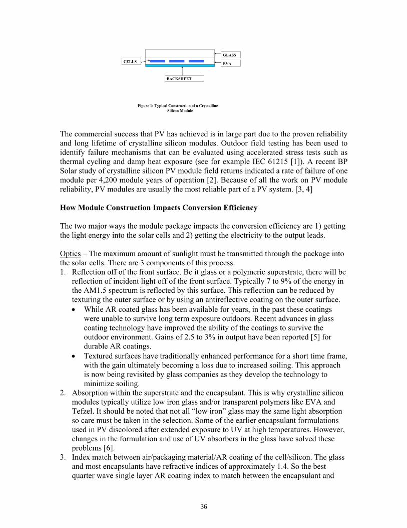
The commercial success that PV has achieved is in large part due to the proven reliability and long lifetime of crystalline silicon modules. Outdoor field testing has been used to identify failure mechanisms that can be evaluated using accelerated stress tests such as thermal cycling and damp heat exposure (see for example IEC 61215 [1]). A recent BP Solar study of crystalline silicon PV module field returns indicated a rate of failure of one module per 4,200 module years of operation [2]. Because of all the work on PV module reliability, PV modules are usually the most reliable part of a PV system. [3, 4] How Module Construction Impacts Conversion Efficiency The two major ways the module package impacts the conversion efficiency are 1) getting the light energy into the solar cells and 2) getting the electricity to the output leads. Optics – The maximum amount of sunlight must be transmitted through the package into the solar cells. There are 3 components of this process. 1. Reflection off of the front surface. Be it glass or a polymeric superstrate, there will be
reflection of incident light off of the front surface. Typically 7 to 9% of the energy in the AM1.5 spectrum is reflected by this surface. This reflection can be reduced by texturing the outer surface or by using an antireflective coating on the outer surface. • While AR coated glass has been available for years, in the past these coatings
were unable to survive long term exposure outdoors. Recent advances in glass coating technology have improved the ability of the coatings to survive the outdoor environment. Gains of 2.5 to 3% in output have been reported [5] for durable AR coatings.
• Textured surfaces have traditionally enhanced performance for a short time frame, with the gain ultimately becoming a loss due to increased soiling. This approach is now being revisited by glass companies as they develop the technology to minimize soiling.
2. Absorption within the superstrate and the encapsulant. This is why crystalline silicon modules typically utilize low iron glass and/or transparent polymers like EVA and Tefzel. It should be noted that not all “low iron” glass may the same light absorption so care must be taken in the selection. Some of the earlier encapsulant formulations used in PV discolored after extended exposure to UV at high temperatures. However, changes in the formulation and use of UV absorbers in the glass have solved these problems [6].
3. Index match between air/packaging material/AR coating of the cell/silicon. The glass and most encapsulants have refractive indices of approximately 1.4. So the best quarter wave single layer AR coating index to match between the encapsulant and
GLASS
EVA
CELLS
BACKSHEET
Figure 1: Typical Construction of a CrystallineSilicon Module
36

silicon is 2.33 (yielding zero reflection at 600 nm). Silicon nitride (with index of 2 to 2.1) used on many of today’s Si solar cells is therefore not a great match and may show a loss of current upon encapsulation. For a double layer system the best index matches (at 600 nm) are 1.96 and 2.75. Most practical double layer AR coating systems have a top layer with a much lower index (1.3 for magnesium fluoride and 1.6 for aluminum oxide). Any advantage gained in using these double layer coatings at the cell level will be lost upon encapsulation.
Electrical – Part of the module packaging includes providing the conductive path for collecting energy from the solar cells. Selection of interconnect material is a compromise between higher conductivity via greater cross-sectional area versus increased shadowing and reduced flexibility. If the cell to cell interconnects are too thick, they are too stiff resulting in cracked interconnects, cracked cells and broken solder bonds. The current paths for cell measurements on a test block may be different than the path in an actual module. These differences will likely include;
• The front contact probe arrangement versus flow to the solder bonds and then through the interconnects. Depending on probes design, the cell measurement can either over or under estimate the cell efficiency.
• Flow in the back metal to the back solder bonds versus directly to a test block. Test block results may not show whether the back metal conductivity is adequate or if it will be a significant source of power loss in the module.
So it is not unusual for the modules to have lower fill factor and therefore lower efficiency than the cells used in the modules. Table 1 shows the fill factor and power for the cells and subsequent 72 cell modules made from these cells. In this case there was no optical loss as an AR coated glass was utilized. Lower fill factor in the modules resulted in 3.5% less power than predicted from the sum of the individual cell powers.
Table 1 Fill Factor and Maxiumum Power for Cells and Modules Built from those Cells
Fill Factor Pmax (%) (W) (%)
Module # Cell Module Cell Module Difference 6325 79.0 75.2 191.6 185.0 3.6 6332 78.8 75.2 190.2 184.6 2.4 5938 79.1 74.8 193.6 185.5 4.2 5969 79.0 74.5 191.2 185.1 3.2 5960 78.9 74.2 191.9 185.1 3.5 5933 79.0 74.8 190.1 184.2 3.1
Average 79.0 74.8 191.4 184.9 3.5
Future Concerns Crystalline silicon PV is heading toward the use of even bigger solar cells. Today many manufacturers are transitioning their production from 12. 5 cm by 12.5 cm cells to 15 cm by 15 cm cells with several displaying preproduction samples of 20 cm by 20 cm cells.
37

This is occurring at the same time that cell efficiencies are increasing meaning the modules of the future are going to be required to handle much higher currents. Table 2 summarizes the transition.
Table 2 Increase in Cell Size and its Impact on Interconnect Cross-Section
Cells Dimensions (cm by cm)
Cell Area (cm2)
Efficiency (%)
Ipmax (A)
Interconnect Cross-Section
(cm2) 10 x 10 100 12.5 2.5 3.6 e-3
12.5 x 12.5 156 14 4.5 5.5 e-3 15 x 15 225 15 6.5 7.9 e-3 * 20 x 20 400 17.5 12.5 15 e-3 *
* These cross-sections are calculated to retain the same percent loss to series resistance in the interconnects as now achieved in the modules using 12.5 cm by 12.5 cm cells.
So to maintain module fill factor the interconnects must have much higher cross-sectional area. Combine this with the problem of getting this current through the cell metallization to the interconnects and it quickly becomes apparent that we if we stay with the 20 year old approach of using 2 or even 3 interconnect tabs running the full length of two cells (the front of one to the back of the next) we are going to lose a much larger percentage of the power to series resistance. What is needed is the development of new approaches to collect and transport the electricity for these larger cells to minimize series resistance loss. Summary Solar cells are utilized as part of a module package. Integration of the cell into the package should be an important part of the overall cell design. Reference: 1. IEC 61215 “Crystalline silicon terrestrial photovoltaic modules- Design qualification and
type approval”, 1993. 2. John Wohlgemuth “Long term photovoltaic module reliability”, Proceeding of the National
Center for Photovoltaics Review Meeting, Denver, CO, March, 2003, p. 179. 3. J. C. Wiles, B. Brooks, B. Schultze, “PV Installations, A Progress Report,” Proceedings of
the 29th IEEE Photovoltaic Specialist Conference, 2002, pp. 1461-1464. 4. A. L. Rosenthal, M. G. Thomas, S. J. Durand, “A Ten Year Review of Performance of
Photovoltaic Systems,” Proceedings of the 23rd IEEE Photovoltaic Specialist Conference, 1993, pp. 1289-1291.
5. C. Ballif, J. Dicker, D. Borchert and T. Hofmann “Solar Glass with Industrial Porous SiO2 Antireflective Coatings: Measurements of Photovoltaic Module Properties Improvement and Modelling of Yearly Energy Yield Gain”, Solar Energy Materials & Solar Cells, Vol. 82, 2004, p. 331.
6. William Holley, Jr., Susan C. Agro, James P. Galica, Robert S. Yorgensen “UV Stability and Module Testing of Non-Browning Experimental PV Encapsulants”, Proceedings of the 25th IEEE Photovoltaic Specialist Conference, 1996, pp. 1259-1262.
38

RELIABILITY ISSUES OF CRYSTALLINE SILICON PV MODULES: A REVIEW
Neelkanth G. Dhere Florida Solar Energy Center, 1679 Clearlake Road, Cocoa, FL 32922-5703
Abstract: Over the years, the reliability and durability of crystalline silicon, c-Si PV modules has improved consistently. Further improvement of service lifetime to 30 years will enhance the value of the modules by 20-50%. This paper reviews the reliability issues in c-Si, photovoltaic (PV) modules and discusses the following topics: Reliability models, delamination caused in a few cases by chemically assisted diffusion of impurities such as phosphorous from dopant and sodium from glass or ambient, degradation of mechanical properties of EVA in hot and dry and especially hot and humid climate, effect of the difference in temperature coefficients of expansion on solder bond strength and on Si wafer breakage and the necessity to test c-Si PV modules under high (>1000 V) voltage bias in hot and humid climate. It also cites a successful example of low degradation in c-Si PV modules after 20 years of deployment at Natural Bridges National Monument in southeastern Utah.
Keywords: c-Si PV modules, reliability, delamination, solder bond, corrosion
Introduction Shipments of PV modules exceeded 740 MW during 2003. Solar cells fabricated on
crystalline silicon, c-Si, consisting of monocrystalline Si and multicrystalline Si wafers constitute the major component of PV module production. The active c-Si solar cell circuit is usually sandwiched between two layers of encapsulant, usually ethylene vinyl acetate (EVA) with glass superstrate in the front and flexible multilayers on the back. Over the years the reliability and durability of c-Si PV modules has improved consistently. Several manufacturers are providing 20-25 year warranties for their PV module. However, warranties are not based on an adequate database. An improvement of service lifetime to 30 years will enhance the value of the modules by 20-50%. It will also validate the economic viability calculations that assume a 30-year lifetime. At present, the beginning-of-life failures have been mostly eliminated by the module qualification tests. However, the end-of-life failure mechanisms that limit module lifetime are not well understood.
Reliability is the ability of a product to perform as intended (i.e., without failure and within specified performance limits) for a specified time, in its life cycle application environment. The physics-of-failure (PoF) approach to reliability utilizes knowledge of the life-cycle load-profile, package architecture, and material properties to identify potential failure mechanisms and to prevent operational failures through robust design and manufacturing practices [1]. It incorporates reliability into the design process, provides scientific basis for estimating product life under actual operating conditions, aids in assessing the possible failure mechanisms due to expected life-cycle stresses and in determining potential causes, locating failures and developing effective tests and screens, and is used for reliability assessment, but not reliability prediction. The "real world" stresses are a high-intensity solar irradiance, ultraviolet (UV) radiation, temperature, humidity, atmospheric gases and pollutants, diurnal and annual thermal cycles and voltage bias. Paradoxically the very materials employed in the fabrication of PV modules in conjunction with external stresses can contribute to performance loss.
Over the last decade, FSEC has accumulated wealth of data through systematic and detailed study of module durability concentrating on the solar cell/encapsulant composite with an
39

objective to lay the scientific basis for improvement of PV module manufacturing technology [2-11]. Crystalline silicon and thin film PV modules are being studied whenever possible with their respective control modules. These include new, acceleration tested modules as well as modules field deployed in hot and humid, and hot and dry climate at FSEC, Sandia National Laboratories (SNL), and other locations in the US and around the globe. Sample extraction process developed by SNL and further improved at FSEC is employed for sample extraction. Morphology of freshly extracted Si cell and EVA samples is examined by optical microscopy, scanning electron microscopy (SEM), Auger electron spectroscopy (AES) using a Perkin Elmer PHI 660 Scanning Auger Multiprobe, and X-ray photoelectron spectroscopy (XPS) using PHI model 560 Multi Technique XPS system. Mechanical properties of EVA are studied on standard Instron testing machine (Model 1122) specially designed for testing polymers. This paper reviews the reliability issues in crystalline silicon (c-Si) PV modules.
Reliability Relevant attributes for reliability assessments include dominant failure mechanisms,
stress drivers for failure and a ranking of time of failure. There are two distinct approaches for estimating the reliability; 1) To collect and analyze actual lifetime data and, from the analysis, establish a failure/time relationship that assumes that the characteristics of the failure rates will remain approximately the same in the future. In this approach, it is not required to determine the root cause of the failure; instead, the sum of all failures is utilized to assess the overall failure rate and 2) To study the mechanism or cause, of failure- particularly the rate at which damage accumulates prior to failure. The point at which failure is reached can then be ascertained exactly, provided one has the knowledge of the initial state of damage, the rate of damage accumulation, and the criterion for when the damage has reached a terminal state [1,12,13].
The reliability of a system can be expressed as a number between 0 and 1, or between 0 and 100%, where the system can be considered as an assembly of entities. Reliability generally decreases with operation or time such that it refers to the probability that a system, or some fraction of an assembly, will function properly at some point in the future. The time-dependent reliability, R(t) is defined as:
R(t) = nsurvivors (t) / ninitial
where 0< R(t) < 1 and ninitial represents the total number of specimens within the assembly [14]. The reliability can also be determined from experimental data representing the distribution of failures as a function of time. This is accomplished by ranking sequentially the experimentally determined failures and then assigning each failure a reliability R, represented by:
R = i / ntotal + 1,
where i is the ranking of the individual failure, ntotal is the number of cases [14]. Analysis of data also provides insight into several other key parameters, such as:
Probability function, f(t) = dR(t) /dt.
Cumulative probability of failure, F(t) = 1 – R(t), or F(t) = 0It f(z) dz
40

Hazard function, h(t) = f(t)/R(t).
The hazard function represents the instantaneous rate of failures and determines the reliability model [14]. For example, when the hazard function, h(t) is constant, λ, then the probability function, f(t) is λeλt and the time-dependent reliability, R(t) is λeλt. Here λ is the fitting parameter. Table I provides hazard functions, h(t), probability functions, f(t), time-dependent reliability, R(t) and the fitting parameters for the typical reliability models [14].
Acceleration Testing
The essential challenges in analyzing the data obtained through accelerated testing are the identification of the appropriate model that will fit the accelerated life data and estimation of the parameters within that model. The acceleration factor, AT may be defined as the ratio between the life time predicted under normal operating conditions and the life time measured under the accelerated condition [14]. For example, for an Arrhenius model the lifetime L(t), is given as the inverse of the hazard rate, h(t)
L(t) = A exp (+Ea/kT)
where A is a fitting parameter, Ea is activation energy of the dominant reaction, k is Boltzmann’s constant, and T is the absolute temperature in Kelvin.
Assuming that the fitting parameter, A and the activation energy, Ea remain constant with temperature, the Acceleration factor AT is given by
AT = exp [Ea/K (1/T0 - 1/Ts)]
Table I: Characteristics of Typical Reliability Models [14].
Hazard Function h(t) f(t) R(t) Fitting
Parameter Constant λ λeλt λeλt λ
Linearly λt
22t
teλ
λ
22t
eλ−
λ
Weibull 1tγγ
θ−
1tγγθ
−t
eγ
θ−
t
eλθ
− γ, θ
Exponential
(b)e-αt
( 1)
( ) tb te
b e eα
α α− − −
( )1b tee
αα
− −
α, b
Arrhenius
( )
aEkTA e
−
( )aEkTA e
− ( 1)[ ]
aEaAE kTe
ke−
−
( 1)eEakTAE e
ke−
−
Ea, A
41

where Ts is the temperature of the accelerated test and T0 is the temperature during service. This expression is often used to evaluate the service lifetime of PV modules, even though the failure modes and mechanisms of PV modules are not yet well understood and the actual failure mechanisms may follow another hazard function [15]. Therefore, it is essential to carry out systematic analysis of field deployed PV modules to understand the failure modes and mechanisms.
Encapsulant A critical component of a PV module is the encapsulant (pottant). It provides structural support, optical coupling, electrical isolation, physical isolation/protection and thermal conduction for the solar cell assembly [15]. The earlier problems of yellowing and browning of EVA caused mainly by UV radiation from the sun have been resolved by using glass doped with ceria, which acts as a UV absorber to prevent photo-degradation as well as by development of encapsulants with UV screens. Analysis of mechanical properties of EVA extracted from new and field deployed PV modules has shown that the mechanical properties such as toughness, resilience, Young’s modulus, total strain, and the ultimate engineering tensile strength (UTS) of EVA can deteriorate considerably after field deployment in hot and dry and especially in hot and humid climate (Table II and Fig. 1) [7,8].
Delamination Delamination has occurred to varying degrees in a small percentage of PV modules. For
example, building integrated PV (BIPV), crystalline silicon, glass-to-glass modules, installed in 1998 and used as a semitransparent façade on the office building of the Federal Ministry of Economic Affairs in Berlin began to show in 2000 partly milky spots due to delamination that grew continuously. [16]. All modules in the 100 kW array were replaced at an estimated cost of US$ 900,000. During the same time period, delamination has been reported in BIPV modules at Bremen, Rheinbach, and PV systems at Troisdorf and Munich, all in Germany [16]. Earlier during 1995-96, all the modules fabricated by another company and installed on one of the segments of a 1 MW plant at Toledo, Spain delaminated. Delamination is more frequent and severe in hot and humid climates.
AES surveys on samples extracted from some modules that had shown considerable delamination after acceleration testing or field deployment in hot and dry or especially hot and humid climate showed high concentrations of phosphorous of >4 atomic (at.)% and of sodium of >14 at.% [6]. Typical AES depth profile of a Si cell sample showed the initial rise, plateau and gradual decline of titanium signal arising from ~1450 Å thick TiOx antireflection (AR) coating (Fig. 2). Initial carbon concentration, arising from coverage of the cell by a very thin ethylene vinyl acetate (EVA) layer, and the substantial sodium concentration initially fell off rapidly and then gradually became negligible at higher depths. Phosphorous concentration decreased rapidly, was negligible within the TiOx AR layer and showed a peak at the TiOx/Si cell interface with maximum concentration as high as 9 at.%. Oxygen concentration showed a narrow peak near the surface followed by a plateau and a decline corresponding to the titanium oxide layer. The oxygen peak near the surface may be the result of oxygen in EVA as well as in compounds formed with the impurities phosphorous and sodium. Similarly oxygen concentration continued to remain significant beyond the TiOx AR layer because of a silicon oxide layer at that interface.
42

Table II Compilation of average mechanical properties of EVA from new and field deployed modules
Sample Toughness Young’s Modulus Total Strain UTS MPa kPa MPa
Uncured 74.3 ± 16.9 10.0 ± 2.4 26.3 ± 2.3 4.5 ± 0.8 New 99.2 ± 41.8 16.5 ± 5.2 23.5 ± 5.6 6.9 ± 1.9 Hot and Dry 10.7 ± 1.6 7.2 ± 0.7 3.9 ± 0.3 4.8 ± 0.4 Hot and Humid 7.7 ± 1.8 8.0 ± 0.6 3.1 ± 0.6 3.6 ± 0.2
AES line scans performed after pausing the depth profiling at the depth of ~50 Å showed
a good correlation in the line scans of Ti and O, and also between the maxima in the carbon concentrations and the minima in the Ti and O concentrations. There was a good correlation between the line scans of sodium and phosphorous (Fig. 3). Figure 4 provides a compilation of adhesional strengths and concentrations of carbon, sodium and phosphorous of samples extracted from acceleration tested modules. It clearly shows that the adhesional strength is higher when carbon concentration at the Si/EVA interface is high and the concentration of sodium and phosphorous is low and vice versa. Similar correlation has been observed in the case of modules deployed in hot and humid, and hot and dry ambients [2-5]. High surface concentrations of sodium and phosphorous, good correlation between concentrations of sodium and phosphorous, often accompanied by proportionately larger concentrations of oxygen in the delaminated samples pointed to formation of compounds such as sodium phosphates and hydro-phosphates. This clearly shows the durability of PV modules could be improved if precautionary measures are taken to control the sources of impurities into the structure of PV modules as well limiting the diffusion of inadvertent impurities. Special precautions would be essential when the silicon feedstock is variable and if recycled wafers are used. The origin of the phosphorous surface concentrations is in the n-type dopant. Sodium may originate from soda-lime glass or from the atmospheric sodium containing aerosols. The diffusion of active species such as sodium and phosphorous would begin satisfying some of the bonds at the EVA and silicon surfaces. This surface passivation would, in turn, reduce the strength of the adhesional bonds. Diffusivity of oxygen, water vapor, and other atmospheric species is high in EVA because it is an amorphous copolymer.
Reaction compounds precipitating at the Si/EVA interface would deplete the sites of adhesional bonds between EVA and silicon cell surface and result in partial delamination. Moreover, voids resulting from the delamination provide a preferential location for accumulation of moisture and precipitation of active impurities. These impurities greatly increase the possibility of corrosion failures in metallic contacts.
Besides limiting the inevitable impurity precipitation arising from diffusion of phosphorous from dopant and sodium from glass and the ambient, it is essential to take adequate precautions to avoid the problem of organic and other contamination during cell and string fabrication and module packaging.
43
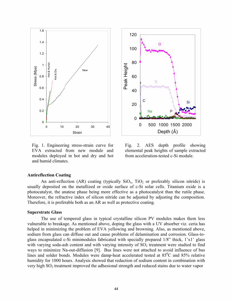
0
0.2
0.4
0.6
0.8
1
1.2
1.4
1.6
0 10 20 30 40
Strain
Stre
ss (M
pa)
New
Hot
& D
ry
Hot
& H
umid
0
20
40
60
80
100
120
0 500 1000 1500 2000Depth (D)
Pea
k H
eigh
t
O
Ti
Na P
SiC
Antireflection Coating An anti-reflection (AR) coating (typically SiOx, TiO2 or preferably silicon nitride) is usually deposited on the metallized or oxide surface of c-Si solar cells. Titanium oxide is a photocatalyst, the anatese phase being more effective as a photocatalyst than the rutile phase. Moreover, the refractive index of silicon nitride can be adjusted by adjusting the composition. Therefore, it is preferable both as an AR as well as protective coating.
Superstrate Glass The use of tempered glass in typical crystalline silicon PV modules makes them less
vulnerable to breakage. As mentioned above, doping the glass with a UV absorber viz. ceria has helped in minimizing the problem of EVA yellowing and browning. Also, as mentioned above, sodium from glass can diffuse out and cause problems of delamination and corrosion. Glass-to-glass encapsulated c-Si minimodules fabricated with specially prepared 1/8” thick, 1’x1’ glass with varying soda-ash content and with varying intensity of SO2 treatment were studied to find ways to minimize Na-out-diffusion [9]. Bus lines were not attached to avoid influence of bus lines and solder bonds. Modules were damp-heat accelerated tested at 850C and 85% relative humidity for 1000 hours. Analysis showed that reduction of sodium content in combination with very high SO2 treatment improved the adhesional strength and reduced stains due to water vapor
Fig. 1. Engineering stress-strain curve forEVA extracted from new module andmodules deployed in hot and dry and hotand humid climates.
Fig. 2. AES depth profile showing elemental peak heights of sample extracted from acceleration-tested c-Si module.
44

0
2
4
6
8
10
12
0 20 40 60 80 100Distance (nm)
Con
cent
ratio
n (a
t.%)
C
Na
P
corrosion (Charles’ effect). Based on this study, AFG completely redesigned their low iron glass composition and lowered the sodium content to ~13% for the entire PV industry [9]. This constitutes a reduction of ~2% in total sodium content.
Backing Layers Backing layers of tedlar/polyester/tedlar or tedlar/polyester/aluminum/tedlar are typically used to protect the backside of c-Si PV module. There are many instances of separation of trilayers, crazing and bubble formation or bulging. Backing sheets containing aluminum foil can be impermeable. Therefore, gaseous reaction products can be trapped inside. Bulging or bubble formation is caused by accumulation of trapped gaseous products in voids caused by delamination. A minimum thickness of aluminium sheet of ~38 µm is essential to assure freedom from porosity. It may be noted that a c-Si PV module may breathe i.e. it may not essential to provide a fully impermeable back protection as long as the moisture does not condense to attain the critical thickness to dissolve contaminants and support ionic conduction. New coated back sheets have the potential to assist in reducing the packaging cost. Therefore, it would be desirable to test them to verify their potential to reduce the cost while guaranteeing reliability.
0
5
10
15
20
25
0.0 2.0 4.0
Shear Strength (MPa)
Na,
P C
once
ntra
tion
(%)
0
10
20
30
40
50
60
70
Carbon C
oncentration(%)
C
P
Na
Fig. 4. Correlation between adhesional strength at Si/EVA interface with concentration of C, Na and P.
Fig. 3. Peak heights of C, Na, and P,obtained from an AES line scanperformed after pausing the depthprofiling at the depth of ~50 Å.
45
Junction Boxes In a few cases, the junction boxes get detached from the PV modules. Attempts to reattach them have not been successful. Providing proper solder-bonded and sealed standard cable connectors would eliminate this problem.
High Voltage Bias Testing in Hot and Humid Climate Grid-connected PV systems, being deployed widely in developed nations, must withstand
high voltage bias in addition to harsh environmental conditions such as intermittent solar irradiance, high humidity, heat, extreme cold, especially diurnal temperature swings, and wind. High leakage currents in biased PV modules can lead to electromigration, corrosion and degradation, and thus become important issues for reliability and safety. Earlier version a-Si:H thin-film PV modules with SnO2:F TCO on the front glass installed on the FSEC High Voltage Test Bed are being monitored since January 2002 [11]. The leakage currents in high-voltage biased PV modules were found to be functions of both temperature and relative humidity. Surface and bulk glass conductivities were found to dominate under wet conditions whereas combination of surface and bulk glass conductivities plus encapsulant/glass interface, sealants, and encapsulant conductances governed under drier conditions. The measured values at noon on clear and cloudy days were lower than the calculated values. On the other hand, the measured values at night on clear and cloudy days were higher than the calculated values. PV module leakage conductance was found to be thermally stimulated with a characteristic activation energy that depends on RH. Crystalline silicon PV modules are less vulnerable to electrocorrosion. However, several of the current paths, electromigration and corrosion mechanisms are common. Moreover, PV modules would be required to demonstrate stability at very high bias voltages exceeding 1000 V. Some of the mechanisms may become more severe at such high biases. Therefore, it would be worthwhile to test c-Si and under high voltage bias exceeding 1000 V in hot and humid climate so as optimize the packaging schemes.
Corrosion and Oxidation Chemical reactions occur between the constituents of the PV module themselves and with
the environment. In all cases, the degree of reaction is the net result of the thermodynamic driving force of the reaction and the actual kinetics of the reaction. Environmental conditions influence moisture ingress and egress [12]. If the moisture is allowed to condense, it together with the corroding material and contaminants controls the rate of corrosion. Humidity plays a vital role in the control of the rate of corrosion. It alone is known to constitute up to 20% of the environmental stresses that along with the temperature lead to device failure in microelectronic packages. Moisture can be trapped in cavities during packaging or can also enter a package by permeation through polymers used in the seals and the package material, or by leakage through cracks or small voids between the plastic materials and leads. The quantity of the contaminants is dependent on construction processes, materials, and operating stresses. Typical problems that can result from exposure to humid environment include: swelling of material due to moisture absorption, failure due to corrosion, degradation of electrical properties in insulating materials, electrical shorts due to condensation, electromigration, accelerated chemical reactions, and chemical or electrochemical breakdown of encapsulant.
For corrosion to occur inside the composite, the moisture has to ingress into the package to support the transfer of ions. Therefore, the time for corrosion failure of a package to occur depends on the time for moisture ingress, or induction time, and the time for the corrosion
46

process. As the temperature increases, the rate of moisture ingress increases and the induction time is reduced. However, corrosion will not occur if the temperature surrounding a potential corroding material is high enough to prevent the formation of a medium. The absolute minimum, or threshold critical value of thickness for the condensed water to dissolve contaminants and support ionic conduction has been estimated to be three monolayers of condensed water molecules. The time required to reach the threshold moisture content depends primarily on the internal volume and leak rate of the package and the environment. During the operation, new leak paths may nucleate and old paths may grow, which decreases the estimated induction time. Corrosion will start when a module is exposed to a temperature below the dew point, so that the moisture inside the package condenses and combines with any ionic contaminant present to provide a conductive path between adjacent metallic conductors. Exposure to sunlight will typically elevate the temperature inside above the dew point. As a result of increase in temperature, electrolyte will evaporate and no longer provide any electrolytic path. The inside temperature is very important factor in controlling the corrosion rate. The thermal corrosion activation function, f*(T), has a value of 0 when the inside temperature is above saturation temperature or below the freezing point and has a value of 1 when the inside package temperature is below the saturation temperature and above the freezing point.
In PV modules corrosion can occur because of acetic acid released from EVA as well as corrosive compounds formed due to diffusion and precipitation of impurities. The scanning electron microscopy image of a grid line in Figure 5 shows a partially corroded grid line with the corrosion products spread on adjacent areas on the cell.
Fig. 5. Scanning electron microscopy image of a corroded grid line
Solder Joint Reliability and c-Si Wafer Breakage The specific purpose of the solder and the ribbon is to form a metallic interconnect
between two adjoining cells. The most widely used solder materials in electronics industry and the US PV industry are 63Sn/37Pb eutectic composition and 60Sn/40Pb near eutectic composition [1,13]. Solder joints in electronic packages are subject to progressive failure by metal fatigue during operation [1]. Solder joint reliability relies not only on intrinsic material properties, but also on design, solder-joint geometry, the soldering process and the long-term service conditions. For a given solder composition and design, the main physical factors affecting the solder material performance are: temperature, humidity, strain range, strain rate, intrinsic microscopic structure and surface condition of materials. The failure processes are: inadequate material strength at given service conditions; excessive disparity in the coefficients of
47
thermal expansion among wafer, solder and bus ribbon; mechanical and/or thermal fatigue due to cyclic strain accumulation; corrosion-accelerated fatigue; excessive intermetallic compound formed at interface; undesirable intermetallic phases formed in the bulk of the solder joint; detrimental microstructure development, and presence of excessive or large-size voids. The degree of uniformity of the solder joint is known to influence the lifetime of the electronic packages. Similarly, the degree of solder joint uniformity would drive the degradation of fill factor of PV modules. In particular, voids within the solder lead to localized heating and consequent increase in creep/relaxation of the solder. In fact, the voids are diminished contact areas and cause current crowding in areas where the solder joint is still good. Extreme caution and care must be exercised during fabrication to avoid the development of such voids.
In some cases, contamination by solder flux has led to bus line discoloration. It can also provide sites for delamination and corrosion.
For brittle materials such as silicon wafers or glass, the fracture criterion is not defined only by the applied stress. An additional parameter, physical dimensions of flaw or defect that causes fracture, is also important. At thicknesses of 200 µm for multicrystalline wafers and 350 µm for monocrystalline wafers the probability of breakage is very low. However, as the wafer thicknesses are reduced, the breakage becomes an important issue. Grid-lines and bus lines are screen-printed or ink-written using thick film silver paste on both sides of c-Si cell wafers to collect the current. Thermal shock during metallization can lead to microcracks. Microcracks can grow at loads below the yield or failure stresses of the wafer because of cyclic fatigue. This happens when wafers are subjected to repeated cycles of stress resulting from thermal expansion coefficient difference and diurnal temperature cycling. Fatigue cracking is time dependent and leads to catastrophic failure of material. It would be useful to detect the microcracks by a suitable technique such as lock-in thermography in combination with ultrasonic vibration.
Because of the substantial difference in the thermal coefficients of expansion between the silicon wafer and the tinned copper ribbon, there is a danger of bowing and breakage of the wafer if the ribbons are soldered continuously along the screen-printed bus lines on the silicon wafer. Therefore, soldering used to be carried out at discreet pads in earlier modules. Recently some manufacturers have begun carrying out the soldering of ribbons continuously and simultaneously along the screen-printed bus lines on both sides of the silicon wafer. In this case, bowing and breaking of silicon wafer is avoided by compensation of stress on one side with an equal and opposite stress on the other side. Moreover, the residual stresses are minimized by limiting the maximum temperature attained during the soldering process. Thick (~200 µm) ribbons are used to carry currents generated in silicon solar cells with substantially enhanced efficiency in recent years, while the Si wafer thickness is being reduced to 200-250 µm or less to minimize cost. This places more stringent limits on the maximum process temperature. The maximum process temperature is being limited while the melting temperature of the solder remains the same. If thermal energy is not applied properly, the probability of bonds not attaining an adequate strength would increases. This is because in that case, all the regions would not attain the requisite temperature for adequate solder flow and for wetting the substrate. Substantially lower solder bond strength has been observed in some field deployed c-Si PV modules. Voids in poor bonds provide nucleation site for corrosive reaction products and moisture, leading to precipitous loss of solder bond strength during field deployment. The problem of low bond strength and Si wafer breakage is likely to become more severe when lead-based solder in PV modules is substituted by silver-based solder so as to maintain the image
48

of being environmental friendly and especially when still thinner Si wafers are employed. It may be noted that the melting point of typical lead-free solder is ~40 oC higher.
Solder bond strength depends not only on the choice of the solder and optimization of the solder bond process but also on the combined optimization of the screen printing and solder bond processes. Therefore, the solder bond process may have to be re-optimized for silicon cells procured though out-sourcing.
A Success Story
Amongst the four types of PV modules initially deployed at the Natural Bridges National Monument (NBNM) in southeastern Utah those manufactured by SpectroLab showed lowest degradation [10]. The average adhesional shear strength of the encapsulant in this module was found to be only ~17% lower than that in new modules. Some corrosion was observed at two solder-joints. Overall the modules have maintained a very high fill factor most probably because of more stringent fabrication process with good uniform solder bonds. Moreover, metallic mesh type interconnection employed in these modules may have provided effective stress relief.
Conclusions At present, the beginning-of-life failures have been mostly eliminated by module
qualification tests. However, the end-of-life failure mechanisms that limit module lifetime are not yet well understood. Therefore, it is essential to carry out systematic analysis of field-deployed PV modules and to learn from the experience of the application of the Physics of failure approach to microelectronic packages so as to understand the failure modes and mechanisms in PV modules and to increase their service lifetime to 30 years. It is recommended that impurities such as phosphorous, sodium, and organic and other contaminants should be adequately controlled so as to avoid delamination and corrosion; solder bond strength should be maintained by properly optimizing the screen printing and solder bonding processes; packaging should be adequate to prevent moisture condensation; new-coated back sheets should be tested to verify their potential to reduce the cost while guaranteeing reliability; and PV modules should be tested under high voltage bias >1000 V so as to optimize the packaging schemes.
Acknowledgements This work was supported by the US Department of Energy through the Sandia National
Laboratories. The author is thankful to Michael A. Quintana and David L. King, SNL, Dr. John Wohlgemuth, BP Solar, and Dr. Alex Mikonovicz, Shell Solar for useful discussions, and to Vinaykumar V. Hadagali and Upendra S. Avachat for help in preparation of the manuscript.
References
1. C. A. Harper, ‘Electronic Packaging and Interconnection Handbook’, McGraw – Hill, Second Edition 1997.
2. N. G. Dhere and N. R. Raravikar, Solar Energy Materials and Solar Cells, 67, (2001), 363.
3. N. G. Dhere, K. S. Gadre, and A. M. Deshpande, Proc. 14th European PV Solar Energy Conference (EPVSEC), Barcelona, Spain, (1997), 256.
49

4. N. G. Dhere, M. E. Wollam, and K. S. Gadre, Proc. 26th IEEE Photovoltaic Specialists' Conference (PVSC), Anaheim, CA, (1997), 1217.
5. N. G. Dhere, Proc. 16th EPVSEC, Glasgow, UK, (2000), 1046. 6. N. G. Dhere and M. B. Pandit, Proc. 17th EPVSEC, Munich, Germany, (2001), 572. 7. N. G. Dhere and K. S. Gadre, Proc. 2nd World PV Solar Energy Conf. Vienna, Austria,
(1998), 2214. 8. N. G. Dhere and K. S. Gadre, Proc. Int. Solar Energy Conf. Solar Engineering 1998,
ASME 1998, Albuquerque, NM, (1998), pp. 491-497. 9. N. G. Dhere, N. R. Raravikar, A. Mikonowicz and C. Cording, Proc. 29th PVSC, New
Orleans, Louisiana, (2002), 231. 10. M. A. Quintana, D. L. King, F. M. Hosking, J. A. Kratochvil, R. W. Johnson, B. R.
Hansen, N. G. Dhere, and M. B. Pandit, Proc. 28th PVSC, Anchorage, Alaska, (2000), 1420.
11. N. G. Dhere, S. M. Bet and H. P. Patil, Proc. 3rd World Photovoltaic Solar Energy Conf. Osaka, Japan, CD, presentation 6P-A9-42, (2003).
12. A. W. Czanderna and G. J. Jorgensen, “Service Lifetime Prediction for Encapsulated Photovoltaic Cells/Minimodules”, Center for performance Engineering and Reliability, National Renewable Energy Laboratory.
13. M. Pecht, ‘Handbook of Electronic Package Design’, Marcel Dekker, Inc. 1991. 14. G. R. Blackwell, ‘The electronic Packaging Handbook’, CRC Press 1999. 15. A. W. Czanderna, F. J. Pern, Solar Energy Materials and Solar Cells, 43, (1996), 101. 16. J. Bernreuter and M. Schmela, Photon International, June 2001.
50

SILICON SUPPLY AND THE WORLD PV INDUSTRY By
PAUL MAYCOCK PV ENERGY SYSTEMS,INC.
“pvenergy.com” The world photovoltaic market is well established: production of cells and modules is strong and installations are growing. Worldwide 2003 module production exceeded $2.3 billion at the factory and over $3.0 billion at retail. The value of installed photovoltaic systems exceeded $6 billion dollars per year in 2003. WORLD CELL/MODULE PRODUCTION. World shipments of photovoltaic cells and modules reached 744 MW in 2003, an increase of 32.4 percent. European production increased 43 % to 193.35 MW. Japanese production growth increased 45 percent to 363.91 MW most of which was used to serve the subsidized PV Home Systems and Institutional Buildings program. United States shipments decreased 15 percent in 2003, due to decreased production by AstroPower as it went through bankruptcy (AstroPower assets and business were purchased by General Electric early in 2004. Production also decreased from the BP Solar owned Solarex plant. Reasons given were retooling and process changes while some production shifted from the US to Europe (the new BP plant in Spain). Rest of World production increased to 84 MW led by the doubling of production of the BP Solar plants in Australia and India and the MoTech plant in Taiwan. FIGURE -ONE: 2003 WORLD PV PRODUCTION (MWp-DC)
Country 1995 1996 1997 1998 1999 2000 2001 2002 2003
U.S. 34.75 38.85 51 53.7 60.8 74.97 100.32 120.6 103.02
Japan 16.4 21.2 35 49 80 128.6 171.22 251.07 363.91
Europe 20.1 18.8 30.4 33.5 40 60.66 86.38 135.05 193.35
ROW 6.35 9.75 9.4 18.7 20.5 23.42 32.62 55.05 83.8
Total 77.6 88.6 125.8 154.9 201.3 287.65 390.54 561.77 744.08 WORLD PV CELL PRODUCTION BY CELL TECHNOLOGY SLICED SINGLE AND POLYCRYSTAL SILICON CONTINUE TO DOMINATE WORLD PV PRODUCTION Nearly 89 percent of the world PV cell and module production was based on sliced single crystal and polycrystal silicon cells (659 MW). Despite the new plants announced in the thin film area, only 26MW of amorphous silicon (3.4%) was produced. In 2003 4 MW of CIS was produced, and 3.0 MW of CdTe was produced. Over 30 MW of Sanyo’s amorphous silicon on crystal silicon slice was produced. Despite several thin film plants ready for production, expansion of single crystal and polycrystal silicon production should continue the dominance of the sliced crystal product for several more years. Over 10,000 metric tons of pure silicon (mostly semiconductor grade silicon scrap) was consumed by the industry in 2003. The author estimates over 30,000 tons will be required in 2010.
51

FIGURE-TWO: 2003 WORLD CELL PRODUCTION BY CELL TECHNOLOGY TECHNOLOGY US JAPAN EUROPE ROW TOTAL
SINGLE CRYSTAL FLAT PLATE 68 44.17 71.15 17.15 200.47 POLYCRYSTAL 13.42 271.23 114.5 60.65 459.8 SINGLE AND POLYCRYSTAL TOTAL 81.42 313.9 182.65 77.8 658.77
AMORPHOUS SILICON outside 7.1 0.01 7.7 3 17.81 AMORPHOUS SILICON INDOOR USE 0 5 0 3 8 AMORPHOUS SILICON TOTAL 7.1 5.01 7.7 6 25.81
CRYSTAL SILICON CONCENTRATORS 0.7 — — — 0.7
RIBBON (SILICON) 6.8 — — — 6.8
CADMIUM TELLURIDE INDOOR 0 0.0* — —
CADMIUM TELLURIDE OUTDOOR 3 — — — 3
COPPER INDIUM DISELENIDE 4 4
MICROCRYSTAL SI /SINGLE SI — 13.5 13.5
SI ON LOW-COST-SUBSTRATE 0 0
A-SI ON Cz SLICE 30 30
Total 103.02 363.91 193.35 83.8 744.08
TOTAL INDOOR USE - 8.0 A-SI +1.5 CdTe 9.6 TOTAL TERRESTRIAL PRODUCTION 734.48
* Matsushita dropped CdTe for calculators SILICON USAGE BY PV INDUSTRY In 2003 660 MW of the cells were made from single crystal or Polycrystal silicon. The industry uses from 12-16 grams per watt of “solar grade” silicon. In our analysis we use 14 grams per watt. The table below shows the silicon usage with a forecast to 2010. The 10,000-13,000 metric tons used now is about 20% of the total silicon (semiconductor grade) used by the world electronic devices industry. This level of consumption is about the limit for the “scrap” used by the PV industry. By 2010 we forecast over 30,000 tons of silicon will be required by the PV industry (Over 80 % of the 3000 megawatts could be crystal silicon using 12 grams per watt..
Materials Consumption for Sliced Crystal Silicon 2003-2010
MATERIAL CONSUMPTION/WATT COST/WATT 2002CONSUMPTION/659MW 2010:2500M
Poly-Si Feedstock 15-20 grams/W $0.30-0.40 9885-13,180 metric tons 30,000 TON
Glass .0007 meters/W $0.03-0.04 46,130 square meters
EVA .0014 meters/W $0.04 92,260 square meters
Aluminum Foil .0007meters/W $0.05 46,130 square meters
Other Materials $0.05
52

TOP TEN PRODUCE 634 MW, 85 PERCENT OF WORLD PV PRODUCT
The top ten producers of PV cells and modules produced 634.42 MW-85 percent of the world production. (Figure E-Three). It is interesting to note that 500 MW of PV is about equivalent to one 500 MW gas turbine used for peaking power (a 20 % capacity factor). Japan companies maintained first and third positions with Sharp’s 198 MW and Kyocera’s 72 MW. BP Solar’s 70.23MW claimed the fourth position with Shell Solar (Siemens Solar) 73 MW in second place. Schott Solar jumped from 7th place to fifth place. Sanyo’s production of its high efficiency amorphous silicon/crystal silicon hetero-junction product gained eighth place. AstroPower dropped from sixth place to eleventh place. Mitsubishi, with 42 MW, tied Schott Solar for 5th place. Q’CELLS joined the top ten by producing 28 MW. Isofoton moved up to 7th place and Photowatt retained their 10th position.
FIGURE THREE: TOP PV CELL/MODULE PRODUCERS PRODUCTION (MW)
COMPANY 1999 RANK 1999
2000 RANK 2000
2001 RANK 2001
2002 RANK
2002
2003 RANK 2003
BP SOLAR 32.5 1 41.9 3 54.2 2 73.8 2 70.23 4
KYOCERA 30.3 2 42 2 54 3 60 3 72 3
SHARP 30 3 50.4 1 75.02 1 123.07 1 198 1
SHELL Solar 22.2 4 28 4 39 4 57.5 4 73 2
AstroPower 12 6 18 5 26 5 29.7 6 17 11
SANYO 13 5 17 6 19 7 35 5 35 8
ISOFOTON 6.1 9.5 10 18.02 8 27.35 8 35.2 7
Photowatt 10 7 14 7 14 10 17 10 20 10
RWE (ASE) 10 7 14 7 23 6 29.5 7 42 5
Mitsubishi ??? ? 12 9 14 9 24 9 42 6
Q,CELLS 28 9
TOTAL 166.1 246.8 336.24 476.92 634.42
WORLD TOTAL 201.3 287.65 390.5 561.77 744.08
The 2003 World Photovoltaic Market by Principal Application Worldwide, shipments of PV modules were about 658 megawatts in 2003. About 65 MW was used in consumer products, such as calculators, watches, other electronic products, small trickle chargers, small lights lanterns, and power packs for motor homes, boats, camping, etc. The remaining 593 MW of outdoor "power" product is a very diffuse market. The “off grid” market sectors include: 30 MW of US off-grid “residential, 70 MW of world off grid rural; 70 MW of remote telecommunications and signals;
53

50 mw of PV Diesel, Commercial. The grid connected residential and commercial exploded to 365 MW owing to subsidy programs in Japan, Germany and the United States. [See Figure E- Three] • Consumer Products Market: (60 MW) PV powers consumer electronics and other small, less than 40
W devices, including lights, signs, security systems, and portable power. We believe that this market will explode when wholesale module prices reach $3/W (presently $5/watt) and the $100 retail price point is broached for 20-watt products.
• U.S. Off-the-Grid “Residential” Market: (20 MW) Small, off-the-grid systems are considered "economic" by the present set of customers with environmental, noise, and other concerns. The US off-the-grid "residential" market represents a moderately large multi-megawatt opportunity for the world PV industry.
• Off-the-Grid Small Market (less than 1kW) (60 MW) : The potential off-the-grid international market is very large compared to the US off-the-grid "residential" market. This market has been very strong in South Africa (1500 kW/year), Indonesia, INDIA, Sri Lanka, Spain (1 MW/year), Italy (500 kW/year), and Scandinavian countries (primarily for outback vacation/resort homes). In developing countries, PV supplies the only alternative for providing minimal electricity in remote homes, farms, and villages.
• Worldwide Communication/Signal Market: (60 MW) The communication/signal market is the current backbone of the “fully economic” PV industry, as systems have already proved to be reliable and economic. Of the annual PV shipments (excluding central station and government projects), communication sales accounted for 30 to 35 percent of total annual revenues until 1997. When the subsidized grid-connected market in Japan and Germany started explosive growth, this sector dropped to 12 percent. Despite this reduction in share owing to the highly subsidized grid-connected product, the communication/signal sector is the “baseline” product that proves the inherent reliability of remote PV.
• World PV Diesel Hybrid/Replacement Market: (45 MW) This application uses the fuel in a diesel or gasoline generator as the storage for a PV system. An advantage over a stand-alone PV system is the reduction in the size of the PV array to supply electricity to loads with the same reliability. This can substantially reduce capital cost while maintaining reliability. Since oil prices have INCREASED after a ten-year decline, the viability of PV systems will be determined primarily by the price reductions in PV modules.
• Grid-Connected Residential/Commercial Market: (275 MW) As a result of the Japanese and German government subsidy programs, this sector has explosively grown to be 51 of the world market.
• Central PV Generation Market: For the US market, we estimate that the “environmental value" of PV could be as high as 20 percent, making the "break even" cost of PV generated electricity, at best, about $0.06/kWh (2002$). As this requires installed systems (NOT MODULES) costs below $2/watt, we cannot forecast any significant use of central PV until WELL AFTER 2010.
54

FIGURE -FOUR: WORLD PV MARKET BY APPLICATION AREA
‘93 ‘96 ‘97 ‘98 ‘99 ‘00 ‘01 ‘02 ‘03 Consumer Products 18 22 26 30 35 40 45 60 65
U.S. Off-Grid Residential 5 8 9 10 13 15 19 22 25
World Off-Grid Rural 8 15 19 24 31 38 45 60 70
Communications and Signal 16 23 28 31 35 40 46 60 70
PV/Diesel, Commercial 10 12 16 20 25 30 36 45 50
Grid-Conn Res, Commercial 2 7 27 36 60 120 199 273 368
Central >100KW 2 2 2 2 2 5 5 5 8
Total (MW/Year) 61 89 126 153 201 288 395 525 658
US PHOTOVOLTAIC ACTIVITIES US PRODUCTION UNITED STATES CELL/ MODULE PRODUCTION TOTALED 103.02 MW IN 2003, WHICH WAS A 20 % DECREASE. THE DECREASE WAS DRIVEN BY THE DIFFICULT YEAR EXPERIENCED BY ASTROPOWER PRIOR TO BANKRUPTCY AND THE REDUCED PRODUCTION BY BP SOLAR CAUSED BY THE PRODUCTION BY NEW PLANTS IN ASIA AND EUROPE AND CHANGES IN THE US SOLAREX PLANT (LARGER SLICES AND A NEW ANTI-REFLECTION COATING). THE PRODUCTION BY MANUFACTURERS IS SHOWN IN FIGURE FIVE. FIGURE - FIVE: US PHOTOVOLTIAC CELL/MODULE PRODUCTION
Company 1996 1997 1998 1999 2000 2001 2002 2003
Shell Solar 17.00 22.00 20.00 22.20 28.00 39.0 46.5 52.0
BP Solar 10.80 14.80 15.90 18.00 20.47 25.22 31 13.42
Solec International 3.50 4.00 4.00 0.60 0.00 0.00 0.00 0.00
AstroPower 2.85 4.30 7.00 12.00 18.00 26.0 29.7 17.0
USSC 0.60 1.70 2.20 3.00 3.00 3.8 4.0 7.0
RWE Schott (ASE) 3.00 4.00 4.00 4.00 4.00 5.0 5.0 4.0
Evergreen Solar 1.9 2.8
First Solar 1.0 3.0
55

Global Solar 2.0
Other 1.1 0.2 0.60 1.00 1.50 1.3 2.5 1.8
TOTAL 38.85 51.00 53.70 60.80 74.97 100.32 120.6 103.02 From PV News, Vol. 23, No 3, Mar 2004. *SunPower, Amonix, Iowa Thin Films, etc. PROGRESS IN THIN-FILM COMMERCIALIZATION
The United Solar Systems Corporation (USSC) 30-MW roll-to-roll amorphous silicon plant produced 7 MW in 2003. The BP Solar amorphous silicon factory in Virginia and their CdTe factory in California, which were closed in late 2002, had zero production. Shell Solar (formerly Siemens Solar Industries) shipped nearly 3 MW of copper-indium-diselenide (CIS) photovoltaic modules. First Solar shipped 3 MW of cadmium telluride (CdTe) modules and announced plans to produce 6 MW in 2004. Global Solar produced nearly 2 MW of CIS on steel modules. Iowa Thin Film Technologies produced about 100 kilowatts for specialty small power applications. One major event in the US thin film market was the joint venture between United Solar and Solar Integrated Power which introduced a new flexible PV roofing material. Over 5 MW is installed on commercial roofs in California.
United States PV Installations Despite the reduced production, the United States installations increased 42 percent from 44.4 MW (not counting systems sized less than 40 watts) in 2002 to 63 megawatts in 2003 (FIGURE SIX). Most of the growth was in the grid-connected sector-from 23 MW in 2002 to 38 MW in 2003. Imported modules doubled to over 18 MW. Most were from Japan. Figure Six shows the US applications by market sector. FIGURE- SIX: Photovoltaic Applications by Market Sector in The United States
APPLICATION 1994 1995 1996 1997 1998 1999 2000 2001 2002 2003 Grid-connected Distributed
1.2 1.5 2.0 2.0 2.2 3.7 5.5 12.0 22.0 32
Off-grid Consumer 3.0 3.5 4.0 4.2 4.5 5.5 6.0 7.0 8.4 9.0 Government Projects 0.6 0.8 1.2 1.5 1.5 2.5 2.5 1.0 1.0 1.0 Off-grid Industrial /Commercial
3.3 4.0 4.4 4.8 5.2 6.5 7.5 9.0 13.0 16.0
Consumer (<40 W)* 1.7 2.0 2.2 2.2 2.4 2.4 2.5 3.0 4.0 4.0 Central Station — — — — — — — — — 5.0 Total Installed in USA 9.4 10.8 13.8 14.7 15.8 21.0 24.0 32.0 48.4 67 IMPORTS 2.0 4.0 5.0 9.0 18.0 EXPORTS 16.2 24.0 25.1 36.3 37.9 39.8 55.0 73.3 81.2 54.0 TOTAL PRODUCED 25.6 34.8 38.9 51.0 53.7 60.8 75.00 100.3 120.6 103
56

INSTALLATION OF PHOTOVOLTAIC SYSTEMS IN CALIFORNIA NEARLY DOUBLED TO 27 MW IN 2003
The California PV program involved several key players and unique assistance. 1.The California photovoltaic “buy down” program resulted in installation of 12.3 MW of grid-connected residential and commercial grid-connected photovoltaic systems. 2.The Sacramento Municipal Utility District (SMUD) completed phase two of its “PV Pioneer” program by offering subsidized photovoltaic systems to its customers at reduced prices SMUD installed about 400 kW of photovoltaic systems in 2003. Over 11 MW of PV systems have been installed by SMUD in the last ten years. 3.The Los Angeles Department of Water and Power (LADWP) PV program (with subsidies as high as $5.50/W) resulted in 3.8 MW of newly installed photovoltaic systems in 2003. Cumulative installations by LADWP reached 7.5 MW. 4.The California Public Utilities RPS program with Pacific Gas & Electric, Southern California Edison, San Diego Gas and Electric, and Southern California Gas Co. installed 9.9 MW in 2003. 5.Other California Utilities and Cities installed nearly 400 kW.
57

The World Photovoltaic Market 1975-2002 Executive Summary
JAPANESE PV ACTIVITIES: PV PRODUCTION EXPLODES TO 364 MW-NEARLY 50% OF WORLD PRODUCTION FIGURE -SEVEN: JAPANESE PV CELL/MODULE PRODUCTION Company 1996 1997 1998 1999 2000 2001 2002 2003
Sanyo 4.6 4.7 6.3 13 17 19 35 35
Kaneka 0 0 0 3.5 5 8 7.5 13.5
Kyocera 9.1 15.4 24.5 30.3 42 54 60 72
Mitsubishi 0 0 ??? ??? 12 14 24 42
Sharp 5 10.6 14 30 50.4 75.02 123.07 197.91
Hoxan 0.8 1 1 1 1 0 0 0
Canon 0.5 2.1 2 1 0 0 0 0
Matsushita 1.2 1.2 1.2 1.2 1.2 1.2 1.5 1.5
Mitsubishi HEL 2
Total 21.2 35 49 80 128.6 171.22 251.07 363.91
Sharp continued its explosion in production to 197.91 MW in 2003 (nearly twice the US production) and announced plans for a module assembly plant in Mexico. Kyocera and Sanyo continued their expansion with announced plans to more than double in the next two years. . Sanyo continued to expand production of its very high efficiency amorphous silicon on crystal silicon hetero-junction (the HIT™ cell). Shipments in 2003 topped 32 MW. The Japanese government goal for PV production is to have production capacity over 500 MW with an in-country market of 250 MW per year and exports of 250 MW by 2005. We estimate that nearly 200 MW of grid connected PV was installed in 2003. As the Japanese “70,000 Roofs” program completes its last year of subsidy, Over 25,000 applicants were approved in FY 2001. (April 2001 to March 2002 and 38,000 applicants were approved in FY 2002. 52,863 applicants were approved in FY 2003. This lead to installations over 200 MW. In 2003 the Japanese industry aggressively sought export sales. Marketing organizations were set up in the United States and Germany. Several government-assisted projects were initiated in the developing world. The figure below summarizes the Japanese residential PV subsidy program. JAPANESE PV RESIDENTIAL DISEMMINATION PROGRAM EXCEEDS GOALS The Japanese PV Systems Dissemination program, started in 1994 (commonly called “the 70,000 Roofs program) exceeded all of its goals. The subsidy program started with a 50% subsidy which was decreased to about 10 percent in FY 2003 (April first 2003-March 31st 2004. Over 168,000 residential systems were installed from 1994-2003 with a total capacity of over 620 MW. The table below was published in “PV Activities in Japan” published by Osamu Ikki [email protected] . (Data from 1994-2001 from the New Energy Foundation.
58

The World Photovoltaic Market 1975-2002 Executive Summary
FIGURE -8 JAPANESE RESIDENTIAL PROGRAM SUMMARY RESIDENTIALPV SYSTEMS
FY94 FY95 FY96 FY97 FY98 FY99 FY00 FY01 FY02 FY03
# INSTALLED 539 1,065 1,986 5,654 6,352 15,879 20,877 25,151 38,282 52,8TOTAL # ACCUMULATED
539 1,604 3,590 9,244 15,596 31,475 52,352 77,503 115,785 168,
MW INSTALLED 1,860 3.916 7.536 19.486 24.123 57.693 74.381 91 141 201MW ACCUMULATED
1.860 5.776 13.312 32.798 56.921 114.614 188.995 280 421 622
We expect aggressive pricing by Japan in order to enter other growing markets. Prices have dropped in Japan for installed residential grid-connected PV systems. Prices in 1995 were nearly $11.00 per watt and installed prices in 2003 were less than $6.00 per watt. The next two years will be pivotal in the Japanese PV industry as the explosive growth in Japan could slow, the new factories come on line, and exports are required to keep the industry vital. EUROPEAN PRODUCTION INCREASES 43 PERCENT PV cell and module production in 2003 increased 43 percent to 193.35 MW. SCHOTT SOLAR and ISOFOTON rose to number one and two in Europe with 38 MW and 35 MW of production. Q CELLS exploded to third place with 28 MWp. Shell grew to fourth place with 25 MW. PHOTOWATT and BP SOLAR SPAIN grew to 20 MW and 16/45 MW. The race for first place in Europe will be very exciting in the next three years. FIGURE NINE: EUROPEAN PV PRODUCTION Company 1997 1998 1999 2000 2001 2002 2003 RWE SCHOTT (was ASE)
2.00 3.00 7.00 10.00 16.00 24.50 38.00
BP Solar (Spain) 11.30 4.50 5.00 9.16 12.16 16.70 16.45
Free Energy Europe 0.60 0.60 0.60 0.60 0.60 0.60 0.60
Intersolar (UK) 1.20 1.30 2.00 2.50 3.00 2.30 2.50
Photowatt-France 5.70 12.00 10.00 14.00 14.00 17.00 20.00
Eurosolare (IT) 2.50 3.20 1.50 2.30 4.00 3.00 3.50
Helios (Italy) 1.40 1.50 1.30 1.50 2.20 3.00 3.50
Isofoton – Spain 2.70 4.20 6.10 9.50 18.02 27.35 35.20
Shell Germany 3.30 7.50 9.00 25.00
Shell Netherlands 2.00 2.00 2.00 2.20 2.80 0.00 0.00
RWE Phototronics (Germany)
0.00 0.00 2.00 2.00 2.00 2.00 2.00
Konkar – Croatia 0.80 0.80 0.80 0.80 0.60 0.60 0.60
59

The World Photovoltaic Market 1975-2002 Executive Summary
SUNWAYS 4.50 4.50
Q CELLS 8.00 28.00
ERSOL 9.00 9.00
Dunasolar (Hungary) 1.20 2.20 3.00 3.00 *??
Other * 0.20 0.40 0.50 0.60 0.50 4.50 4.50
Total 30.40 33.50 40.00 60.66 86.38 135.05 193.35* Dunasolar Eqpt moved to Thailand
EUROPEAN INSTALLATIONS TOP 140 MW European installations are estimated at 140 MW with over 100 MW in Germany, and 20 MW in the rest of Europe in 2003. GERMAN PV PROGRAM MOVES BEYOND THE “100,000 ROOFS LEVEL) The German subsidized PV installations are estimated at nearly 120 MW in 2003, permitting Germany to exceed their goal of 350 MW installed. As this was the last year of the low-interest, high price for PV electricity (about 45 cents $US per kWh) the German program was re-born in January 2004 with a new law, which dropped the interest subsidy and extended the buy back rate at 45 to 62 Eurocents per kWh. The table shows the new rate structure. (Note there are still some minor changes being made in the law, but it appears that nearly unlimited growth in the German PV and wind programs is probable in the next five years or so. FEED-IN TARIFFS (euro cents/kWh) UNDEVELOPED
AREA ROOFTOP<30 KW
ROOFTOP> 30 KW
FACADES < 30 KW
FACADES> 30 KW
PARLIAMENTARY BILL
45.7 57.4 55.0 62.4 60.0
REST OF WORLD PV PRODUCTION The Rest of World PV production in 2003 increased by 69 percent to 55 MW (FIGURE NINE). MOTECH reported over 200% growth to 8.0 MW. We increased China production to 8.0 MW. (We had unconfirmed reports of over 10 MW in production). Much of the growth in ROW production was the increased production of BP Solar in India (13.1 MW), Australia (8.4 MW). Hong Kong, and Malaysia. (We thank BP Solar for their detailed matrix of production by plant throughout the world).
FIGURE -TEN: REST-OF-WORLD PV CELL/MODULE PRODUCTION
Company 1995 1996 1997 1998 1999 2000 2001 2002
CEL (India) 1.40 1.60 2.00 2.00 2.10 1.50 1.7 1.5 SINONAR (Taiwan) 2.50 2.50 2.60 2.00 3.00 3.0 3.0
BHEL (India) 1.15 1.00 1.00 1.00 1.00 1.00 1.5 1.5 BEL (INDIA) 1.0
60

The World Photovoltaic Market 1975-2002 Executive Summary
RES (India) 0.70 1.00 1.00 1.20 1.20 1.00 1.0 ?? HELIODINAMICA 0.40 0.10 0.00 0.00 0.00 0.00 0.0 0.0
REIL (India) 0.70 0.70 - - ?? ?? ?? ?? China 1.50 1.50 1.50 1.60 2.00 2.50 3.0 8.0
WEBEL (India) 0.65 0.70 0.70 1.20 1.50 1.2 3.0 UDHAYA (India) 0.50 0.50 0.50 0.50 0.50 0.5 .95
BP SOLAR (India) 3.80 4.00 6.46 8.06 13.1 BP SOLAR (Australia) 5.10 5.50 5.76 6.96 8.4
BP SOLAR (HONG KONG) 1.3 3.3 BP SOLAR (MALAYSIA) 0.7 1.3
MOTECH 3.5 8.0 Other 0.50 0.20 0.20 0.20 0.20 0.20 0.2 2.0* Total 6.35 9.75 9.40 18.70 20.50 23.42 32.62 55.05
PV NEWS, V22, NO3, MAR 2003 * INCLUDES MICROSOL, HARBIN CHRONAR, MAHARISHI CONCLUSIONS DESPITE THE UNCERTAINTY CAUSED BY THE NATIONAL AND STATE PV SUBSIDY PROGRAMS OUR FORECAST TO 2010 IS FOR CONTINUED GROWTH AT A COMPUND GROWTH RATE OF OVER 25 PERCENT. THE OFF-GRID MARKET SECTORS WILL CONTINUE TO GROW AT THE 15-20 PERCENT LEVEL WHILE THE GRID CONNECTED SEGMENTS WILL GROW AT LEVELS APPROACHING 50% PER YEAR. Owing to the dramatic increase in the German and US grid-connected markets there is a near term shortage of PV modules. Prices have increased from a low of $2.60 per watt to the $3.00 level (factory).New or small customers are on allocation. HOWEVER, PRICES FOR CRYSTAL SILICON MODULES WILL SLOWLY DROP FROM THE $2.60-$2.75/ DC WATT LEVEL TO $2.20/WATT BY 2010. WE EXPECT PROFITABLE THIN FILM PRICES BELOW $2.00 PER WATT TO BE OFFERED IN 2005/6 AND POSSIBLY TO DROP TO $1.75 PER WATT BY 2010. CRYSTAL SILICON (SINGLE AND POLY CRYSTAL) CELLS WILL CONTINUE TO DOMINATE THE WORLD PRODUCTION THROUGH 2010. WE ESTIMATE THAT 2500 MW WILL BE PRODUCED WITH SINGLE AND POLYCRYSTAL SILICON MATERIAL. AT 12 GRAMS/WATT THE INDUSTRY WILL NEED 30,000 TONS OF “SOLAR GRADE” SILICON. FIGURE- ELEVEN; PV ENERGY SYSTEMS FORECAST TO 2010
61

The World Photovoltaic Market 1975-2002 Executive Summary
Market Sector 1990 1993 1996 1998 2000 2002 2005* 2010* Consumer products 16 18 22 30 40 60 105 250U.S. off-grid residential 3 5 8 10 15 25 45 110World off-grid rural 6 8 15 24 38 60 110 260Communicate/signal 14 16 23 31 40 60 90 220PV/diesel, commercial 7 10 12 20 30 45 80 110Grid-connectedresidential, commercial 1 2 7 35 120 270 550 2000Central >100 kW 1 2 2 2 5 5 20 50Forecast (MW/yr) 48 70 100 150 250 1000 3000Actual (MW/yr) 48 61 89 152 288 525 ---- ---- Forecast avg price ($/W) – – – – 3 2 1.5Forecast low price ($/W) – – – – 2 1.75 1.25Actual avg price ($/W) 4.5 4.25 4 4 3.5 3.25 – –
62

1
August 2004
NREL - 14th Workshop on Crystalline Silicon Solar Cells & Modules: Materials and Processes
Breaking the PV Paradigm - Organic Photovoltaics: A disruptive technology on the horizon
Harvesting the Most Abundant and Available Energy on Earth.
Harvesting the Most Abundant and Available Energy on Earth.
© Global Photonic Energy Corp., 2004 - Confidential3
GPEC is a technology development company monetizing intellectual property through technology transfer and licensing.
CreateIP
CreateCreateIPIP
ProtectIP
ProtectProtectIPIP
LicenseIP
LicenseLicenseIPIP
Business Model
© Global Photonic Energy Corp., 2004 - Confidential4
GPEC Vision
To be the leading provider of organic photonic-energy conversion technologies serving Photovoltaic (PV) Cell manufacturers and Energy companies producing the Photo Fuel™ - Hydrogen
Company Vision
Transform The Energy IndustryTransform The Energy Industry
63

2
© Global Photonic Energy Corp., 2004 - Confidential5
Intensive efforts have successfully resulted in declining manufactured costs and a vibrant, rapidly growing PV market.
-
500
1,000
1,500
2,000
2,500
3,000
3,500
4,000
1976
1977
1978
1979
1980
1981
1982
1983
1984
1985
1986
1987
1988
1989
1990
1991
1992
1993
1994
1995
1996
1997
1998
1999
2000
2001
2002
2003
$-
$5
$10
$15
$20
$25
$30
$35
$40
$45
Source: Paul Maycock, PV News; NREL data; T. Peterson, Strategies Unlimited and Katalyst analysis
Sales
Cost
— PV Industry Sales & Cost Trends —
1976 – 2003 CAGRsProduction 33%Sales 22%Cost -9%
~$4 billion
Situation
© Global Photonic Energy Corp., 2004 - Confidential6
The silicon-based technology introduced by Bell Labs now dominates the global PV market.
cSi, 92.9%
CdTe, 0.8%CuInSe, 0.5%
aSi, 5.8%
— Technology Share of PV Market—
Source: Paul Maycock, PV News, 2002 production data
Situation
© Global Photonic Energy Corp., 2004 - Confidential7
PV generated energy has yet to become a significant energy portfolio player.
• 0.01% of Global primary energy demand
• Very small portion of US electricity production
• Only 12% of global production and 11% of installations is in the U.S.
Complication
— PV Power Position —
© Global Photonic Energy Corp., 2004 - Confidential8
PV’s impact as an energy source has been slowed by several factors.
• Price/kWhr remains high relative to alternatives– Significant production scale is just starting to appear
– Path to lower cost relatively clear
• Limited form factors
• Successful business case leverage
• Technology – vs. – Customer-Application orientation
Growth Challenges
— PV Industry Challenges —
64

3
© Global Photonic Energy Corp., 2004 - Confidential9
To transform the PV industry to the next level of business performance a new approach and technological breakthroughs are needed.
Customer-ApplicationSolutions Approach
DisruptiveTechnologicalBreakthrough
Major Global Energy
Role
Transformation
© Global Photonic Energy Corp., 2004 - Confidential10
To grow faster, the PV industry could benefit from a more customer and application specific orientation.
Source: Dr. Raymond Sutula
Market
Applications
Systems
Subsystems
Components
Materials & Processes
Market
Applications
Systems
Subsystems
Components
Materials & Processes
What is the population of flat commercial roofs by state and utility?
What are the high-value uses of solar on flat commercial roofs?
What are the performance and cost characteristics of a flat-roof solar system for heat and/or power?
What are the key factors in an inverter? A mounting subsystem? A heat recovery element?
How does a component like inverter software impact costs for interconnection? Reliability?
Are thin-films reliable components of roof systems?Can insulation/weatherproofing and module production be integrated to lower costs?
A New Approach
— Systems Driven Approach —
© Global Photonic Energy Corp., 2004 - Confidential11
Organic Photovoltaics (OPVs) is the disruptive technological innovation that could change the PV business and lead to incremental market growth.
• New Application Capabilities
• New Manufacturing & Process Capabilities
• New Cost Trajectory
— Organic PVs —
Organic PVs
© Global Photonic Energy Corp., 2004 - Confidential12
Thank You!
65
Recent Insights into Thin Film Silicon Growth from Phase Diagrams for Plasma-Enhanced Chemical Vapor Deposition
R.W. Collins,1 G.M. Ferreira,2 A.S. Ferlauto,2 C. Ross,3 and C.R. Wronski2 1 Department of Physics and Astronomy, The University of Toledo, Toledo, OH 43606, USA. 2 Center for Thin Film Devices, Penn State University, University Park, PA 16802, USA; 3 Institut für Photovoltaik, Forschungszentrum Jülich, 52425 Jülich, Germany; Abstract Phase diagrams are convenient for categorizing the evolution of the surface microstructure and phase with accumulated thickness for hydrogenated silicon (Si:H) films during plasma-enhanced chemical vapor deposition (PECVD). They can also be used to assess the electronic quality and device suitability of Si:H thin films in both the amorphous phase (a-Si:H) and in the microcrystalline phase (µc-Si:H) for applications in photovoltaics. In this study, as an example, phase diagrams have been applied in a comparison of higher rate (6.5 Å/s) Si:H PECVD using two different plasma excitation frequencies, rf at 13.56 MHz and vhf at 60 MHz. Smooth crystalline Si (c-Si) wafer substrates have been used in this study to obtain the roughness evolution on Si:H surfaces with the highest sensitivity. This study has shown that, for films prepared on c-Si substrates with a range of [H2]/[SiH4] flow ratios in the vicinity of the a → (a+µc) transition, vhf and rf a-Si:H films exhibit remarkably similar structural and phase evolution with thickness, as long as the plasma power levels are chosen for the same deposition rates in the vhf and rf processes. Introduction The deposition phase diagram concept for Si:H PECVD involves plotting one or more structural or phase transition boundaries in the plane of the H2-dilution flow ratio R=[H2]/[SiH4] and the accumulated bulk layer thickness db [1]. R is the deposition parameter exerting the strongest influence on the phase evolution and so is the natural one to be used as the diagram’s abscissa. The extended version of the Si:H deposition phase diagram applied in the present study includes three transitions versus accumulated thickness. These transitions are detected by real time spectroscopic ellipsometry (RTSE) from the time evolution of the surface roughness on the Si:H films and from the dielectric functions extracted at different stages in the growth process. (i) The amorphous roughening transition thickness [denoted a → a] provides insights into the device suitability of a-Si:H materials. Earlier correlations have shown that the highest device-quality a-Si:H exhibits the most stable surface and so the largest a→a roughening transition thickness. A large a → a roughening transition is believed to be associated with a long SiH3 precursor surface diffusion length in the growth process, and this association may account for the earlier correlations. (ii) The amorphous−to−(mixed-phase-microcrystalline) roughening transition [denoted a → (a+µc)] identifies the optimum R value for a-Si:H deposition under otherwise fixed conditions. This optimum generally occurs at the maximum R value just before the a → (a+µc) transition is crossed for the given thickness [1-3]. At this R value, the largest a → a transition thickness inevitably occurs. The observed decrease in the a → (a+µc) transition thickness with increasing R has led to new concepts in multistep processing for optimum a-Si:H. In such procedures, a very high value of R (R ~ 40) is employed for a thin layer at an interface or in a multilayer; R is then reduced (to R < 10) before microcrystallites nucleate within the layer [4,5].
66

(iii) The (mixed-phase)−to−(single-phase) microcrystalline smoothening transition [denoted (a+µc) → µc] serves to identify optimum conditions for the fabrication of µc-Si:H materials. These conditions occur near the (a+µc) → µc transition in such a way that a thin a-Si:H component is maintained at the boundaries of the crystallites for passivation purposes [6,7]. In this case, the observed decrease in transition thickness with increasing R has led to the concept of multistep processing that employs the highest values of R (R ~ 100-200) only in the initial stages to ensure nucleation of predominantly µc-Si:H. Then R is reduced in a stepwise fashion (to R ~ 15) to prevent the layer from evolving to single phase µc-Si:H, in which case the a-Si:H grain boundary phase is lost [8]. Smooth c-Si substrates avoid substrate-induced surface roughness in the growing Si:H films and thus provide the highest sensitivity to each of the three transitions listed above. It must be emphasized, however, that the phase diagrams for the range of R near and above the a → (a+µc) transition depend sensitively on the substrate. Thus, to explore the conditions under which optimized a-Si:H and µc-Si:H thin film solar cells are fabricated, one must use the same substrate structure as is used in the devices. The goal of this investigation is to explore the effects of excitation frequency on Si:H PECVD in greater detail, comparing results for the microstructural evolution of f = 60 MHz (vhf) and f = 13.56 MHz (rf) Si:H materials. In order to increase the deposition rate of Si:H by PECVD, thus increasing the throughput of solar cell production and lowering its costs, very high frequency (vhf) plasma excitation, typically within the range of 50 < f < 100 MHz, has been adopted as an alternative to conventional radio frequency (rf) excitation at f = 13.56 MHz [6,7,9,10]. Vhf excitation is generally considered to be more efficient in dissociating SiH4+H2 mixtures, thus permitting higher rate PECVD of a-Si:H and µc-Si:H. Experimental Details
Two deposition series were studied in detail in this comparison of phase diagrams for vhf and rf PECVD Si:H on native-oxide-covered c-Si and R=0 a-Si:H substrates held at 200°C. For both series, the films were prepared in a single-chamber reactor having parallel-plate electrodes with a fixed spacing of 1.9 cm. For the first series, only c-Si substrates were used in order to compare the physical processes of deposition. High plasma power levels (0.53-0.72 W/cm2) and an elevated total pressure (3 Torr) were used in this first series, yielding identical rates for vhf and rf PECVD of 6.5 Å/s just before the a → (a+µc) boundaries, which both occur at R=60 for the thick (4000 Å) films of this series. The deposition rate trends vs. R for these vhf and rf PECVD films are shown in Fig. 1(a). In the second series, which included depositions on both c-Si and R=0 a-Si:H, minimum plasma power (0.08 W/cm2) and low total gas pressures (< 1.0 Torr) were used, yielding rates of 0.5 Å/s (rf) - 2 Å/s (vhf) just before the a → (a+µc) boundaries, which both occur at R=10 for thick (4000 Å) films. In this deposition series, the partial pressure of SiH4 was fixed at ~0.03-0.07 Torr, and the total pressure ranged from 0.07 to 0.96 Torr with the increase in R from 0 to 40. The deposition rates vs. R for the vhf and rf PECVD films of this series prepared on c-Si are shown in Fig. 1(b). The evolution of the surface roughness and bulk layer thicknesses (ds, db), as well as the complex dielectric function ε = ε1 + iε2 of the Si:H film in different growth regimes, were obtained using a multichannel ellipsometer in the rotating-compensator configuration (spectral range: 1.5 to 4.8 eV). Data analysis details have been provided elsewhere [1].
67

Fig. 1: Si:H deposition rate vs. H2-dilution ratio R comparing vhf (60.0 MHz) and rf (13.56 Hz) PECVD for two conditions of total pressure ptot: (a) ptot = 3 Torr under two different plasma power conditions that yield a common growth rate of ~6.5 Å/s for both sets of depositions just below the a → (a+µc) transition (at R=60, in both cases); (b) ptot < 1.0 Torr using the minimum plasma power of 0.08 W/cm2 for both vhf and rf depositions, yielding growth rates of 1.9 Å/s (vhf) and 0.5 Å/s (rf) at R=10, just below the thick film a → (a+µc) transition in both cases. Results and Discussion To establish a better understanding of the basic differences between the vhf and rf PECVD processes for Si:H films, elevated pressure (3 Torr) vhf and rf conditions were employed that yield essentially identical, relatively high deposition rates of 6.5 Å/s at R=60 just below the a → (a+µc) transition for 4000 Å thick films [see Fig. 1(a)]. Figure 2(a) shows the microstructural evolution, specifically, the surface roughness layer thickness (ds) versus db deduced by RTSE for the growth of the rf (13.56 MHz) PECVD Si:H films at different H2-dilution levels (R=15, 20, 40, and 60). All four films remain amorphous throughout the bulk layer thickness evolution, as indicated by their dielectric functions. Figure 2(b) shows the microstuctural evolution of rf PECVD Si:H films deposited using H2-dilution levels of R=70, 80, and 100 under otherwise identical conditions as those in Fig. 2(a). Each of these films crosses the a → (a+µc) transition during the growth, at a transition thickness that decreases with increasing R. Only the deposition with R=100 also crosses the (a+µc) → µc transition during growth, at a thickness of ~700 Å in this case. The physical processes underlying the behaviors in Fig. 2 will be discussed in greater detail in the following paragraphs. In Fig. 2(a), three manifestations of improved material quality are clearly evident with increasing R right up to the a → (a+µc) transition: (i) increased surface smoothening (both amplitude and rate) associated with the coalescence of initial a-Si:H nuclei in the first 100 Å of deposition; (ii) reduced surface roughness layer thickness in the stable surface regime; and (iii) increased thickness db at which the a → a roughening transition occurs.
(a) (b)
68

Fig. 2: Surface roughness layer thickness (ds) versus bulk layer thickness (db) for deposition of a-Si:Hfilms on (native oxide)/c-Si substrates by rf (13.56 MHz) PECVD using H2-dilution levels of (a) R=15,20, 40, and 60; and (b) R=70, 80, and 100; at a plasma power of 0.72 W/cm2 and a total pressure of 3.0Torr.
Fig. 3: Evolution of the surface roughnessthickness predicted in a 1-d theoretical model forRTSE of Si:H film growth, starting from initialsemicircular nuclei 20 Å in radius positioned in alinear array with 40 Å spacing and with 1%random modulations in the nuclei height. Thismodel assumes a competition between smoothen-ing due to surface diffusion with length λ0 androughening due to shadowing by cluster pro-trusions.
Fig. 4: Relation between the amorphousroughening transition thickness and the surfacediffusion length for the film growth model ofFig. 3. Two different results are shown here,depending on whether the amorphous roughen-ing transition is identified by a 0.5 Å increasein the surface roughness layer thickness overthe stable surface value, or by a 1 Å increase.
(a) (b)
69

These three characteristics can be understood from one-dimensional continuum models of film growth in the following general way (see, e.g., [11-13]). Low amplitude surface modulations A(λ,t) of spatial wavelength λ less than a critical value L are unstable and decay as a function of time t (or thickness) according to A(λ,t) ~ A0(λ)expω(λ)t, where ω(λ) < 0 for λ < L. Features with λ > L, such that ω(λ)>0, are enhanced. Typically, the highest rate of enhancement occurs for features with wavelength just above L, and the development of features with this correlation length generates the roughening transition (iii) above. Under most deposition conditions, the correlation length associated with the initial nuclei is less than L and the smoothening of these surface features generates the effects (i) and (ii) above. In a more specific model, the smoothening effects can be attributed to surface diffusion, which exhibits a (−a4λ-4) term in ω(λ), and the roughening effects can have a number of causes, one possibility being shadowing by protrusions, which exhibits a (+a2λ-2) term in ω(λ) [12]. Considering a simple model with only these two sources of roughness evolution, the diffusion length λ0 is determined by the balance of the two terms (i.e., by ω=0 or L=λ0). Figure 3 demonstrates the predicted roughness evolution from such a one-dimensional model, using as the starting condition semicircular nuclei an average of 20 Å in height positioned on a 40 Å linear array. These nuclei with λ ~ 40 Å < L smoothen during coalescence, whereas roughening occurs via statistical fluctuations in the height of the nuclei with λ > L. In more complicated models, the diffusion length does not enter in such a straightforward manner [11]. In any case, when the surface diffusion length increases in the a-Si:H deposition process, an effect that leads to improved quality materials, the onset of roughening shifts to longer times or greater thicknesses. This behavior is demonstrated in Fig. 4 for the roughness evolution model of Fig. 3. In Figure 2(b), the roughening onsets for all three depositions with R=70, 80, and 100 can be attributed to the a → (a+µc) transition in which microcrystallites nucleate from the amorphous phase and grow preferentially, leading to crystallite protrusions on the surface. The smoothening effect, observed only for the R=100 deposition, is attributed to the (a+µc) → µc transition in which case the preferentially growing crystallites make contact and coalesce. Figure 5 shows a schematic of the relation between the surface roughness evolution as deduced from RTSE and the microstructural evolution for a Si:H deposition (from the second series) that evolves through all three growth regimes [a-Si:H, (a+µc)-Si:H, µc-Si:H] versus thickness. Due to the preferential crystallite growth, crystallites develop cone-like structures in the mixed-phase growth regime, behavior that is also evident in cross-sectional transmission electron microscopy (XTEM) studies. The shifts to lower thickness with increasing R in both the a → (a+µc) and the (a+µc) → µc transitions are associated with an increase in the nucleation density of the crystallites that leads to a narrower range of thickness over which the mixed-phase growth regime occurs. From simple geometric considerations, one can extract the nucleation density and cone angle from the RTSE data, specifically from the two bulk-layer transition thicknesses and the roughness layer thicknesses at these two transitions. As shown in Fig. 6 for a wider set of depositions, the results for these geometric parameters are consistent with selected XTEM studies of single depositions and atomic force microscopy (AFM) studies of a series of depositions made to different thicknesses under the same conditions.
70
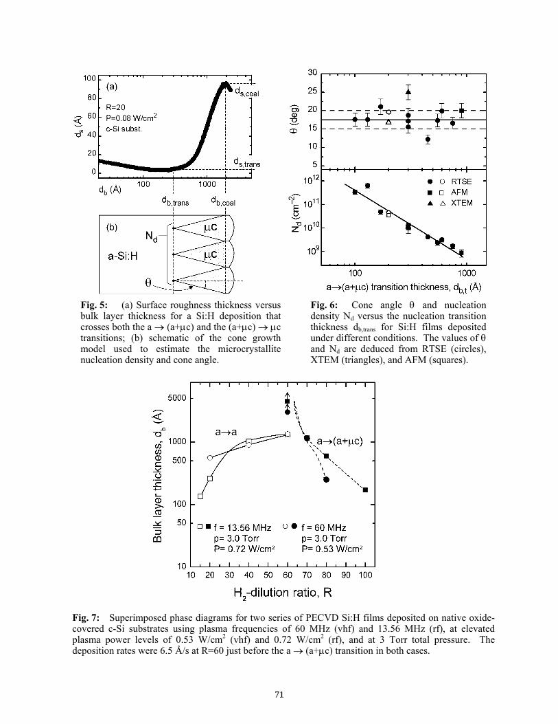
Fig. 7: Superimposed phase diagrams for two series of PECVD Si:H films deposited on native oxide-covered c-Si substrates using plasma frequencies of 60 MHz (vhf) and 13.56 MHz (rf), at elevatedplasma power levels of 0.53 W/cm2 (vhf) and 0.72 W/cm2 (rf), and at 3 Torr total pressure. Thedeposition rates were 6.5 Å/s at R=60 just before the a → (a+µc) transition in both cases.
Fig. 5: (a) Surface roughness thickness versusbulk layer thickness for a Si:H deposition thatcrosses both the a → (a+µc) and the (a+µc) → µctransitions; (b) schematic of the cone growthmodel used to estimate the microcrystallitenucleation density and cone angle.
Fig. 6: Cone angle θ and nucleationdensity Nd versus the nucleation transitionthickness db,trans for Si:H films depositedunder different conditions. The values of θand Nd are deduced from RTSE (circles),XTEM (triangles), and AFM (squares).
71

The results for the surface roughness evolution of vhf (60 MHz) PECVD Si:H exhibit similarities to those of Figs. 2, obtained from rf (13.56 MHz) PECVD Si:H. Thus, the vhf results will not be presented in detail here. Instead, the focus will be on the final results of the comparison, the superimposed phase diagrams for the vhf and rf deposition processes that yield identical rates of 6.5 Å/s at R=60 just below the a → (a+µc) transitions [see Fig. 1(a)]. The key observation from these two overlapping phase diagrams presented in Fig. 7 is that both rf and vhf PECVD a-Si:H films exhibit identical a→a roughening transition thicknesses at the optimum R value of 60 just before the a → (a+µc) transition. On the basis of this observation, one can conclude that both R=60 depositions exhibit similar material quality, and that vhf PECVD provides no significant advantage over rf PECVD for a-Si:H when high rate deposition conditions are optimized and identical deposition rates are compared. In addition to this key conclusion, two additional features are evident in Fig. 7. First, at the lowest value of R accessible to vhf PECVD (R=20), the a → a roughening transition thickness for vhf deposition is significantly higher than that for rf deposition, suggesting that under non-optimal conditions, in particular an insufficient H2-dilution level, the vhf process does provide an improvement over the corresponding rf process. Second, at the highest value of R accessible to vhf PECVD (R=80), the a → (a+µc) occurs at a lower thickness for vhf PECVD than for rf suggesting a higher density of crystallites nucleating from the amorphous phase in the case of vhf PECVD. This in turn suggests advantages of vhf over rf PECVD for the fabrication of µc-Si:H.
Figure 8 shows results for the second series of Si:H films. In this case, both vhf (60 MHz) and rf (13.56 MHz) plasma frequencies were used for growth on R=0 a-Si:H. For these depositions, a minimum plasma power (0.08 W/cm2) and low total gas pressures (< 1.0 Torr) were used, yielding rates of 0.5 Å/s (rf) - 2 Å/s (vhf) just before the a → (a+µc) boundaries, which both occur at R=10 for thick (4000 Å) films. Overall the thicknesses of the a → (a+µc) and (a+µc) → µc transitions for the two different frequencies are in good agreement. The only significant difference in Fig. 8 occurs with R=15 in which case the a → (a+µc) transition is shifted to lower thickness for the higher frequency. The close similarities of the results in Fig. 8 suggest that multistep optimization procedures for the i-layers of a-Si:H and µc-Si:H solar cells would apply equally well for vhf and rf deposition processes. The multistep process expected to apply for the optimization of the i-layers of a-Si:H solar cells is based on the concept that one achieves continuous improvements in material quality and stability with increasing R in the a-Si:H growth regime [4]. As a result, alternations between a thin (~ 100 Å) R=40 layer and an even thinner (< 50 Å) crystallite nucleation suppression layer at R~5 is expected to provide improved performance and stability a-Si:H materials [5]. Similarly multistep processes are expected to apply for the optimization of the i-layers of µc-Si:H solar cells, as well. In this case, for example, p-layer depositions with R=160-200 are found to lead to immediate nucleation of microcrystals on ZnO [14], however, to prevent loss of the a-Si:H grain boundary material with increasing thickness during the i-layer deposition, R can be reduced in a series of steps [8] even to as low as R ~15. This multistep process serves two roles: (i) it ensures that grain boundary regions are passivated with an amorphous phase, and (ii) it ensures maximum rates and minimum deposition times for a thick µc-Si:H i-layer.
72

Acknowledgments This research was supported by NREL Subcontracts XAF-8-17619-22, NDJ-1-30630-01, and AAD-9-18-668-09; and by NSF Grant DMR-0137240. References [1] R. W. Collins, A.S. Ferlauto, G.M. Ferreira, C. Chen, J. Koh, R.J. Koval, Y. Lee, J.M. Pearce, and
C.R. Wronski, Sol. Energy Mater. Sol. Cells 78, 143 (2003). [2] Y. Lu, S. Kim, M. Gunes, Y. Lee, C. R. Wronski, and R. W. Collins, Mater. Res. Soc. Symp. Proc.
336, 595 (1994). [3] D. V. Tsu, B. S. Chao, S. R. Ovshinsky, S. Guha, and J. Yang, Appl. Phys. Lett. 71, 1317 (1997). [4] J. Koh, Y. Lee, H. Fujiwara, C. R. Wronski, and R. W. Collins, Appl. Phys. Lett. 73, 1526 (1998). [5] K.H. Jun, J.D. Ouwens, R.E.I. Schropp, J.Y. Lee, J.H. Choi, H.S. Lee, and K.S. Lim, J. Appl. Phys.
88, 4881 (2000). [6] O. Vetterl, F. Finger, R. Carius, P. Hapke, L. Houben, O. Kluth, A. Lambertz, A. Muck, B. Rech,
and H. Wagner, Sol. Energy Mater. Sol. Cells 62, 97 (2000). [7] A. Shah, J. Meier, E. Vallat-Sauvain, C. Droz, U. Kroll, N. Wyrsch, J. Guillet, and U. Graf, Thin
Solid Films 403, 179 (2002). [8] B. Yan, G. Yue, J. Yang, S. Guha, D.L. Williamson, D. Han, and C.-S. Jiang, Mater. Res. Soc.
Symp. Proc. 808, A8.5 (2004), [9] X. Deng, S.J. Jones, T. Liu, M. Izu, and S.R. Ovshinsky, in: Conf. Record of the 26th IEEE
Photovoltaic Specialists Conference, (IEEE, 1997) p. 591. [10] M. Fukawa, S. Suzuki, L. Guo, M. Kondo, A. Matsuda, Sol. Energy Mater. Sol. Cells 66, 217
(2001). [11] B. J. Palmer and R. G. Gordon, Thin Solid Films 158, 313 (1988). [12] A. Mazor, D. J. Srolovitz, P. S. Hagan, and B. G. Bukiet, Phys. Rev. Lett. 60, 424 (1988). [13] R. W. Collins and B.-Y. Yang, J. Vac. Sci. Technol. B 7, 1155 (1989). [14] P. I. Rovira, A. S. Ferlauto, R. J. Koval, C. R. Wronski, R. W. Collins, and G. Ganguly, Mater. Res.
Soc. Symp. Proc. 609, A19.6 (2000).
Fig. 8: Superimposed phase diagram for Si:H depositions on R=0 a-Si:H substrate films using vhf (60MHz) and rf (13.56 MHz) plasma excitation. For these depositions, a minimum plasma power (0.08W/cm2) and low total gas pressures (< 1.0 Torr) were used, yielding rates of 0.5 Å/s (rf) - 2 Å/s (vhf) justbefore the a → (a+µc) boundaries, which both occur at R=10 for thick (4000 Å) films.
73

Toward Better Understanding and Improved Performance of Silicon Heterojunction Solar Cells
T.H. Wang1, M.R. Page1, E. Iwaniczko1, D.H. Levi1, Y. Yan1, H.M. Branz1
V. Yelundur2, A. Rohatgi2, G. Bunea3, A. Terao3, and Q. Wang1 1National Renewable Energy Laboratory, 1617 Cole Blvd., Golden, CO 80401
2Georgia Institute of Technology, 777 Atlantic Dr., Atlanta, GA 30332 3SunPower Corporation, 430 Indio Way, Sunnyvale, CA 94085
Abstract
The double-sided silicon heterojunction (SHJ) solar cell is more appropriate for n-
type crystal silicon (c-Si) wafers than for p-type c-Si wafers because there is a larger band offset to the valence band edge of hydrogenated amorphous silicon than to the conduction band edge. Thin intrinsic and doped hydrogenated amorphous silicon (a-Si:H) double layers by hot-wire chemical vapor deposition (HWCVD) are investigated as passivation layers, emitters, and back-surface-field (BSF) contacts to both p- and n-type wafers. Passivation quality is studied by characterizing the SHJ solar cells and by photoconductive decay (PCD) minority-carrier lifetime measurements. The crystal-amorphous heterointerface is studied with real-time spectroscopic ellipsometry (RTSE) and high-resolution transmission electron microscopy (HRTEM) to detect phase change and material evolution, with a focus on better understanding the factors determining passivation effectiveness. A common feature in effective passivation, emitter, and BSF layers is immediate a-Si:H deposition and an abrupt and flat interface to the c-Si substrate. In this case, good wafer passivation or an excellent heterojunction is obtained, with a low interface recombination velocity (S) or a high open-circuit voltage (Voc). Voc greater than 640 mV, S less than 15 cm/sec, and efficiency of 14.8% have been achieved on polished p-type Czochralski-grown (CZ) Si wafers. Collaboration between NREL and Georgia Tech resulted in a 15.7%-efficient HWCVD-deposited SHJ cell on non-textured FZ-Si with a screen-printed Al back surface field (BSF), the highest reported HWCVD SHJ cell. Collaboration between NREL and SunPower demonstrated that HWCVD a-Si:H passivation can be better than the conventional oxides, with a low surface recombination velocity of 42 cm/sec on textured n-type FZ-Si.
1. Introduction
The most important material property for photovoltaic (PV) silicon, minority carrier
lifetime, is strongly affected by the thermal history of the silicon substrate because of various defect-impurity mechanisms such as H-O centers, B-O complexes, thermal donors, and metal-dopant pairs. Ulyashin et al. [1] demonstrated that significant enhancement in minority carrier lifetime can be achieved by thermally annealing silicon substrates in N2 at 450ºC for 20 min; increases of 200%, 150%, and 200% in lifetime were seen for CZ-Si, FZ-Si, and multicrystalline silicon, respectively. Schultz et al. [2] showed that by lowering the normal 1050ºC oxidation for 1 hour to 800ºC for 4 hours, the dramatic lifetime degradation of 65% by 1050ºC oxidation was cut to 5% loss only for multicrystalline silicon, highlighting the potential advantages of low-temperature processing. Various lifetime enhancement techniques like P-gettering and H-passivation from SiNx:H which are commonly used for PV
74

silicon impose difficult constraints on the temperature sequences used in the other device processing steps. If polycrystalline thin-film silicon on inexpensive, low-temperature substrates is achieved, low-temperature device processing will be essential. With the current industry trend toward thinner wafers or ribbons, wafer bowing caused by high-temperature metal back contact is a great concern. The a-Si:H/c-Si heterojunction solar cell is a good solution to these problems because a-Si:H deposited below 250ºC can be used as the junction emitter, the passivation layer, and the full contact BSF. The simple planar structure of the SHJ may also help control processing costs.
2. Status of silicon heterojunction solar cells
The SHJ solar cell grew out of research on a stacked amorphous/crystalline silicon
cell design by Hamakawa et al. [3,4] in 1983. In 1990, a more advanced silicon heterojunction device structure was developed by Sanyo as the Heterojunction with Intrinsic Thin-layer (HIT) cell, with a doped a-Si(doped)/µc-Si(undoped)/crystalline Si structure [5]. In 1991, Sanyo changed their µc-Si:H undoped layer to a-Si:H [6]. According to Taguchi et al [7], in the normal a-S:H/c-Si heterojunction cells, the open-circuit voltage (Voc) and fill factor were lower than those of conventional diffused solar cells. These poor properties are a result of the recombination process throughout the depletion region at the a-Si/c-Si heterojunction. Moreover, doped a-Si layers have mid-gap state densities above 1018 cm-3 [8] that would increase dark tunneling leakage currents. This tunneling process is suppressed by inserting the intrinsic a-Si:H spacer which contains only 1015 to 1016 cm-3 of midgap defect levels. With this intrinsic a-Si:H spacer, a Voc of 600 mV and 1-cm2-cell efficiency of 14.8% was soon demonstrated on an n-type CZ-Si wafer [9]. Sanyo then successfully applied the HIT structure to the backside of the cell as a back surface field (BSF) layer. By using the HIT structure on both sides of the cell with a highly reflective metal as the back electrode and by optimizing other conditions, they obtained an open-circuit voltage of 644 mV and an efficiency of 20% for an aperture area of 1 cm2 [9]. In late 1997, Sanyo started mass production and have since achieved laboratory cell efficiency of 21.3% on 100-cm2 cell area and an open-circuit voltage of 714 mV. The production cell and module efficiencies are 19.5%, and 17%, respectively. These results are for n-type CZ-Si after refinements to their process that include reduced H-plasma damage, low-temperature screen-printed metal grids of 2-mm spacing, and steps to upgrade minority carrier lifetime of the wafers [10].
Inspired by the outstanding performance of the HIT cells, dozens of research groups
[11, 12] throughout the world have been trying to duplicate Sanyo’s results with only partial success so far, due to insufficient understanding of the heterointerface and lack of open literature about critical surface pretreatments and other process steps. In addition, because p-type silicon is a more common PV material, SHJ cells on p-type c-Si are more popular than on n-type. But it has been difficult to achieve high efficiency with double-sided HIT cells on p-type c-Si. Nevertheless, with a high-temperature BSF (such as alloyed Al or diffused B), SHJ cells based on p-type c-Si have been encouraging. For example, on a textured p-type CZ-Si with an Al-BSF, Tucci et al. [13] made a 17% efficient 2.25-cm2 SHJ solar cell with a Voc of 600 mV by using a CrSi2 thin layer to enhance the emitter conductance. A 1-cm2 cell that is 15.9% efficient with a Voc of 612 mV has also been reported on textured p-type CZ-Si with a boron-diffused BSF [14].
75
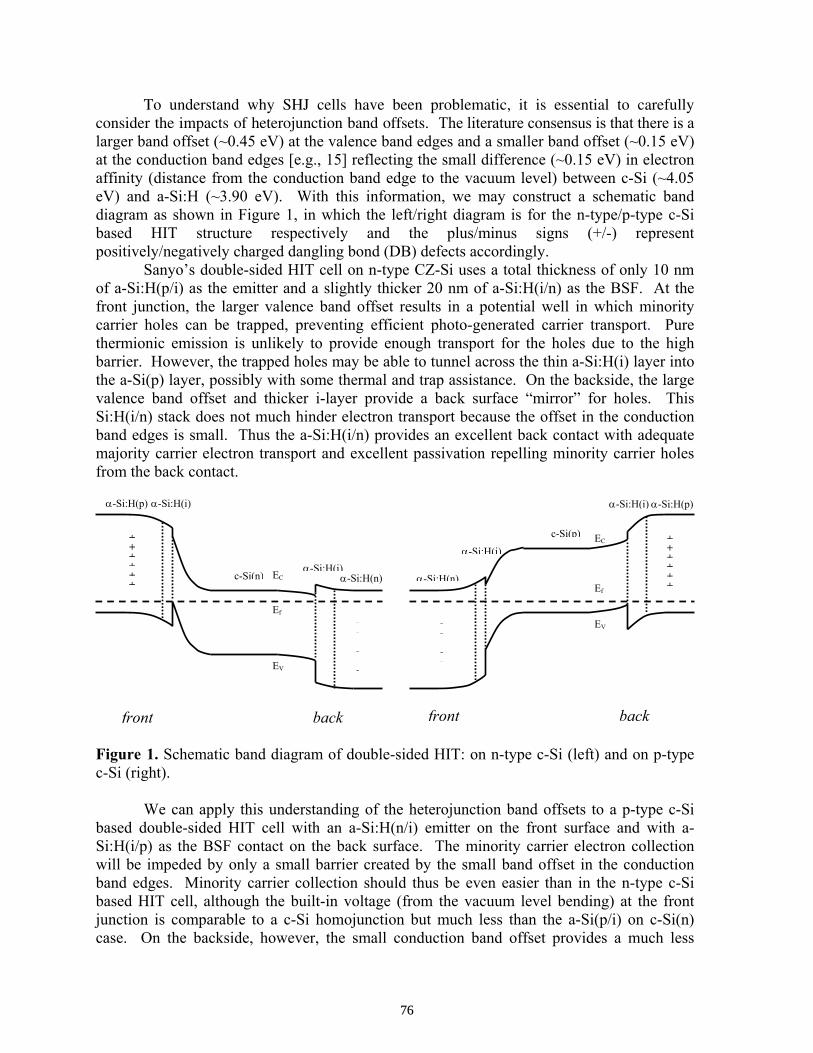
To understand why SHJ cells have been problematic, it is essential to carefully consider the impacts of heterojunction band offsets. The literature consensus is that there is a larger band offset (~0.45 eV) at the valence band edges and a smaller band offset (~0.15 eV) at the conduction band edges [e.g., 15] reflecting the small difference (~0.15 eV) in electron affinity (distance from the conduction band edge to the vacuum level) between c-Si (~4.05 eV) and a-Si:H (~3.90 eV). With this information, we may construct a schematic band diagram as shown in Figure 1, in which the left/right diagram is for the n-type/p-type c-Si based HIT structure respectively and the plus/minus signs (+/-) represent positively/negatively charged dangling bond (DB) defects accordingly.
Sanyo’s double-sided HIT cell on n-type CZ-Si uses a total thickness of only 10 nm of a-Si:H(p/i) as the emitter and a slightly thicker 20 nm of a-Si:H(i/n) as the BSF. At the front junction, the larger valence band offset results in a potential well in which minority carrier holes can be trapped, preventing efficient photo-generated carrier transport. Pure thermionic emission is unlikely to provide enough transport for the holes due to the high barrier. However, the trapped holes may be able to tunnel across the thin a-Si:H(i) layer into the a-Si(p) layer, possibly with some thermal and trap assistance. On the backside, the large valence band offset and thicker i-layer provide a back surface “mirror” for holes. This Si:H(i/n) stack does not much hinder electron transport because the offset in the conduction band edges is small. Thus the a-Si:H(i/n) provides an excellent back contact with adequate majority carrier electron transport and excellent passivation repelling minority carrier holes from the back contact.
Figure 1. Schematic band diagram of double-sided HIT: on n-type c-Si (left) and on p-type c-Si (right).
We can apply this understanding of the heterojunction band offsets to a p-type c-Si
based double-sided HIT cell with an a-Si:H(n/i) emitter on the front surface and with a-Si:H(i/p) as the BSF contact on the back surface. The minority carrier electron collection will be impeded by only a small barrier created by the small band offset in the conduction band edges. Minority carrier collection should thus be even easier than in the n-type c-Si based HIT cell, although the built-in voltage (from the vacuum level bending) at the front junction is comparable to a c-Si homojunction but much less than the a-Si(p/i) on c-Si(n) case. On the backside, however, the small conduction band offset provides a much less
c-Si(p)
α-Si:H(n)
α-Si:H(p)
α-Si:H(i)
α-Si:H(i)
Ef
EC
EV
++++++
------
front back
α-Si:H(n)
++ ++++
c-Si(n)
α-Si:H(p) α-Si:H(i)
α-Si:H(i)
Ef
EC
EV
------
front back
76

effective mirror for the minority carrier electrons. Worse, the larger offset in the valence band edges would present a large barrier for majority carrier holes to flow through to the back contact unless one sacrifices passivation by using a thinner or no i-layer to use trap-assisted tunneling. An alternative is to use a-SiC:H [16] or other alloys with bigger conduction band offsets to c-Si as the BSF for p-type c-Si. If, indeed, the band offset is much larger in the valence band edges than in the conduction band edges then: (1) a-Si(n/i) will be a good emitter for p-type c-Si with a built-in voltage comparable to a silicon homojunction; (2) a-Si(p/i) with a very thin i-layer will be a very good emitter for n-type c-Si with a higher built-in voltage than a silicon homojunction; (3) a-Si(i/p) is a poor BSF for p-type c-Si; and (4) a-Si(i/n) is an ideal BSF for n-type c-Si.
All the amorphous layers in the better performing heterojunction cells reported so far
have been deposited by plasma-enhanced chemical vapor deposition (PECVD). Obtaining high performance of such cells by HWCVD, in which precursor gases (e.g., silane) are decomposed by a hot W filament at about 2000°C, has been a challenge [17, 18]. However, HWCVD could prove superior to PECVD for silicon heterojunction solar cells because of higher deposition rates, reduced ion bombardment of the base wafer, and high densities of atomic hydrogen (H) generation that may passivate the wafer interface region.
3. Collaborative research at NREL, Georgia Tech, and SunPower
For the reasons discussed above, we began our silicon heterojunction solar cell work at NREL with an a-Si(n/i) emitter on Al-BSF p-type c-Si, even though a completely low-temperature heterojunction process is the ultimate goal. We focus on emitter and BSF optimization with effective interface passivation. With a more complete understanding and control of the HWCVD heterointerfaces, we can apply them to other types of devices including a double-sided HIT structure. One problem that HWCVD presents is a tendency to grow epitaxial silicon on clean c-Si substrates [19], even at temperatures as low as 200°C. In high-efficiency heterojunction solar cells, a thin (~5 nm) intrinsic hydrogenated a-Si:H layer must be interposed between the base wafer and the heavily doped emitter, as discussed above. If epitaxy extends through the i-layer, the defective interface will be contacted by the doped a-Si:H which is a much less effective passivant than the intrinsic layer. Partial epitaxy, highly defective epitaxy, or a mixed phase i-layer can all cause detrimental high dark currents, because the a-Si/c-Si interface area or defect density will be large. The additional dark-current path through inadequately passivated interface states leads to a low Voc. Therefore, Voc and the interface recombination velocity (S) are important indicators of the effectiveness of an a-Si:H/c-Si heterointerface. Our earlier HWCVD effort yielded 13% efficiency and a Voc of merely 580 mV [18]. After careful interface studies, we achieved Voc over 640 mV [20], S below 15 cm/sec, and efficiency of 14.8% on p-type CZ-Si with no surface texturing and single layer anti-reflection coating (ARC). Collaboration with Georgia Tech has resulted in a 15.7% cell on non-textured p-type FZ-Si with a Georgia Tech screen-printed Al-BSF and single layer ARC. This is believed to be the highest reported efficiency for a HWCVD silicon heterojunction cell [21]. We expect still better performance when we incorporate surface texturing and double-layer ARC. Working with SunPower Corp’s randomly textured FZ-Si samples, we obtain a surface recombination velocity of 42 cm/sec, lower than the value of 52
77

cm/sec by high-temperature oxidation followed by forming gas annealing.
3.1.Effect of crystallinity in Si layer The crystallinity of the deposited Si layer is found to be very sensitive to the crystal orientation of the substrate. In one set of experiments, RTSE clearly indicates epitaxial growth up to 30 nm in thickness on a (100) substrate at 250°C. On a (111) substrate at the same temperature, however, RTSE shows the film to be essentially a-Si as soon as the deposition starts. When the substrate temperature is higher, epitaxial growth can also be observed on (111) substrates. In Figure 2a, the single-crystal silicon characteristic peaks at 3.38 eV and 4.25 eV in the imaginary part of the pseudo-dielectric function, <ε2>, calculated directly from the measured parameter Ψ and ∆ by RTSE, persists for 1.5 min (~15 nm) at 500°C on a (111) wafer, enduring the i-layer (5 nm) and extending well into the n-layer. This is confirmed by the HRTEM image of Figure 2b. As a result, the Voc of this device is only 487 mV.
Figure 2. Si deposition on a (111) wafer at 500°C: (a) <ε2> evolution. Arrow shows start of growth; (b) HRTEM image. Line shows the wafer surface. As shown in Figure 3, when we lowered the substrate temperature to 100°C for both the i- and n-layer deposition, abrupt amorphous silicon growth is obtained, even on a (100) wafer. A Voc of 628 mV is obtained on this device. Because of the tendency to grow epitaxial Si at higher HWCVD temperatures, Voc decreases with increasing emitter deposition temperature. Figure 4 is a plot of Voc as a function of the i- and n-layer deposition temperatures (same for both layers) for 1.0 and 0.4 Ω⋅cm (111) substrates. The best voltage is obtained for substrate temperatures of 100 to 150°C. Once an epitaxial film is grown through the intrinsic layer and into the doped layer because of too high a deposition temperature, Voc is limited to 600 mV or lower, depending on the a-Si/c-Si interface roughness and quality of the epitaxy. With carefully chosen conditions to avoid epitaxial growth, we have achieved Voc exceeding 640 mV on p-type CZ-Si. The beneficial effect of an abrupt interface is shown in interface recombination velocity S. Figure 5 shows the S value as a function of i-layer deposition temperature, for passivations with the n-layer temperature fixed at 300ºC(*). Reducing the i-layer temperature reduces S as Si epitaxy is suppressed. (*The higher n-layer temperature is used for dopant
78
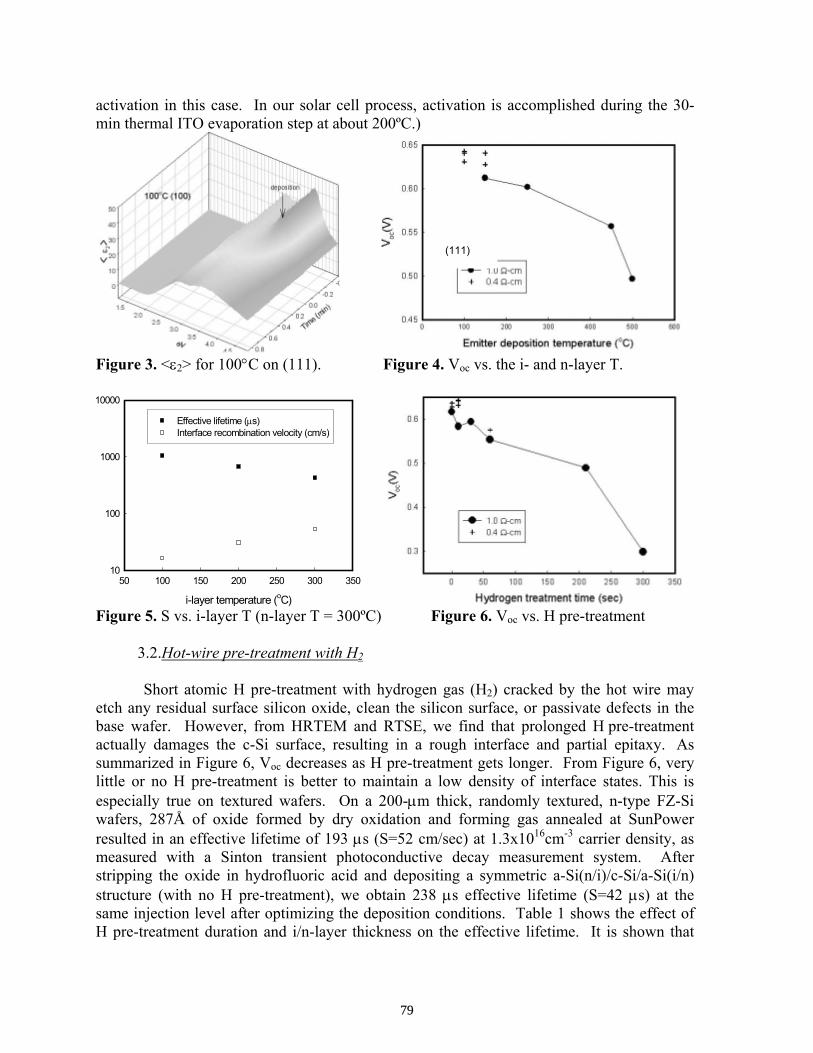
activation in this case. In our solar cell process, activation is accomplished during the 30-min thermal ITO evaporation step at about 200ºC.)
Figure 3. <ε2> for 100°C on (111). Figure 4. Voc vs. the i- and n-layer T.
i-layer temperature (oC)
50 100 150 200 250 300 35010
100
1000
10000
Effective lifetime (µs)Interface recombination velocity (cm/s)
Figure 5. S vs. i-layer T (n-layer T = 300ºC) Figure 6. Voc vs. H pre-treatment
3.2.Hot-wire pre-treatment with H2
Short atomic H pre-treatment with hydrogen gas (H2) cracked by the hot wire may etch any residual surface silicon oxide, clean the silicon surface, or passivate defects in the base wafer. However, from HRTEM and RTSE, we find that prolonged H pre-treatment actually damages the c-Si surface, resulting in a rough interface and partial epitaxy. As summarized in Figure 6, Voc decreases as H pre-treatment gets longer. From Figure 6, very little or no H pre-treatment is better to maintain a low density of interface states. This is especially true on textured wafers. On a 200-µm thick, randomly textured, n-type FZ-Si wafers, 287Å of oxide formed by dry oxidation and forming gas annealed at SunPower resulted in an effective lifetime of 193 µs (S=52 cm/sec) at 1.3x1016cm-3 carrier density, as measured with a Sinton transient photoconductive decay measurement system. After stripping the oxide in hydrofluoric acid and depositing a symmetric a-Si(n/i)/c-Si/a-Si(i/n) structure (with no H pre-treatment), we obtain 238 µs effective lifetime (S=42 µs) at the same injection level after optimizing the deposition conditions. Table 1 shows the effect of H pre-treatment duration and i/n-layer thickness on the effective lifetime. It is shown that
(111)
79

any H pre-treatment seems to lower the effective lifetime or increase the S value. Table 1. Effect of H2 treatment and i/n-layer growth time (in seconds) on effective lifetime
H2 at 100°C i-layer at 100°C n-layer at 300°C Effective lifetime (µs) 10 10 210 136.8 10 30 210 92.5 10 10 420 95.5 10 10 315 133.9 5 15 210 136.6 0 10 210 237.9 20 10 210 122.0
4. Summary
If the valence band offset is larger than the conduction band offset, a-Si(n/i) and
a-Si(p/i) can be good emitters for p-type c-Si and n-type c-Si wafers, respectively. However, although a-Si(i/n) will be an excellent back contact for n-type c-Si, a-Si(i/p) will make a poor back contact to p-type c-Si. The large valence band offset at the c-Si(p)/a-Si(i/p) interface will present a large barrier to hole collection and the small conduction band offset will provide an inadequate minority carrier mirror.
A common feature in effective passivation, emitter, and BSF layers is immediate
a-Si:H deposition and an abrupt and flat interface to the crystalline silicon (c-Si) substrate. In this case, good wafer passivation or an excellent heterojunction is obtained with a low interface recombination velocity or a high Voc. Reduced Voc or increased S is found whenever the heterointerface is not abrupt and flat. Wafers at higher temperature and with (100) orientation are more likely to lead to deleterious epitaxial growth than those at lower temperature or with (111) orientation. A short (10 s) H2 treatment with the hot wire prior to the a-Si:H film deposition may improve carrier transport across the interface, but prolonged treatment can damage the c-Si surface, leading to a rough interface with partial epitaxy, reduced Voc, and higher S. Textured c-Si surface is especially adversely affected by H2 treatment. With these findings, Voc greater than 640 mV, S less than 15 cm/sec, and efficiency over 15.0% have been achieved on polished p-type Czochralski-grown (CZ) Si wafers. Collaboration between NREL and Georgia Tech produced an SHJ cell with efficiency above 15.7% on non-textured FZ-Si with a screen-printed Al-BSF. This is the highest reported efficiency for an HWCVD-deposited silicon heterojunction cell. We expect still better performance when we incorporate surface texturing and double-layer ARC. A collaboration between NREL and SunPower demonstrated a low surface recombination velocity of 42 cm/sec on textured n-type FZ-Si by a-Si:H passivation. Acknowledgements
The authors would like to thank Charles Teplin, Yueqin Xu, Scott Ward, Anna Duda, Richard Ahrenkiel, Steve Johnston, Richard Crandall, and Daniel Friedman for their valuable
80
technical assistance and discussions. This work is supported by U.S. DOE under Contract #DE-AC36-99G010337. References [1] A. Ulyashin, R. Bilyalov, A. Brück, M. Scherff, R. Job, W. Fahrner, J. Poortmans,
Proceedings CD of the 3rd World Conf. PV Energy Conv., 4p-A8-69, Osaka, Japan, May 11-18, 2003
[2] O. Shultz, S.W. Glunz, J.C. Goldschmidt, H. Lautenschlager, A. Leimenstoll, E. Schneiderlöchner, G.P. Willeke, 19th European PV Solar Energy Conf., 2DO.3.2, Paris, France, June 7-11, 2004
[3] K. Okuda, H. Okamoto, Y. Hamakawa, Jap. J. Appl. Phys., Vol. 22 No. 9 (1983) L605 [4] Y. Hamakawa, H. Okamoto; K. Okuda, United States Patent 4,496,788, January 29,
1985 [5] M. Iwamoto, K. Minami, T. Yamaoki, United States Patent 5,066,340, November 19,
1991 [6] S. Noguchi; H. Iwata, K. Sano, United States Patent 5,213,628, May 25, 1993 [7] M. Taguchi, K. Kawamoto, S. Tsuge, T. Baba, H. Sakata, M. Morizane, K. Uchihashi,
N. Nakamura, S. Kiyama, and O. Oota, Prog. Photovolt: Res. Appl. 2000; 8: 503-513 [8] K. Pierz, W. Fuhs and H. Mell, J. Non-Cryst Solids; 114 (1989) 651 [9] T. Sawada, N. Terada, S. Tsuge, T. Baba, T. Takahama, K. Wakisaka, S. Tsuda, S.
Nakano, Proceedings of the 1st World Conf. PV Energy Conv., Hawaii, 1994, 1219 [10] M. Tanaka, S. Okamoto, S. Tsuge and S. Kiyama, Proceedings CD of the 3rd World
Conf. PV Energy Conv., Osaka, May 11-18, 2003 [11] N. Jensen, R.M. Hausner, R.B. Bergmann, J.H. Werner, and U. Rau, Prog. Photovolt:
Res. Appl. 2002; 10:1-13 [12] F. Roca, J. Cárabe, A. Jäger-Waldau, 19th European PV Solar Energy Conf., Paris,
France, June 7-11, 2004 [13] M. Tucci, G. de Sasere, J. Non-Cryst. Solids, Vol. 338-340 (2004) 663 [14] M.L.D. Scherff, A. Froitzheim, W. R. Fahrner, 19th European PV Solar Energy Conf.,
June 7-11, 2004, Paris, France [15] M. Sebastiani, C. RiGaspare, G. Capellini, C. Bittencourt, F. Evangelisti, Phys. Rev.
Lett. 75 (1995) 3352 [16] M. Cuniot and N. Lequeux, Philosophical Magazine B, 64, 6 (1991) 723 [17] C. Mukherjee, U. Weber, H. Seitz, B. Schroder, Thin Solid Films, 395 (2001) 310 [18] Q. Wang, M.R. Page, Y. Xu, E. Iwaniczko, E. Williams, T.H. Wang, Thin Solid Films,
430 (2003) 208 [19] J. Thiesen, E. Iwaniczko, K.M. Jones, A. Mahan, R. Crandall, Appl. Phys. Lett., 75
(1999) 992 [20] T.H. Wang, Q. Wang, E. Iwaniczko, M.R. Page, D.H. Levi, Y. Yan, C.W. Teplin, Y. Xu,
X.Z. Wu, and H.M. Branz, 19th European PV Solar Energy Conf., 2CV.3.54, Paris, France, June 7-11, 2004
[21] M.R. Page, E. Iwaniczko, Q. Wang, D. Levi, Y. Yan, H.M. Branz, V. Yulundur, A. Rohatgi, and T.H. Wang, This Workshop, Winter Park, CO, August 8-11, 2004
81

Wright Williams & Kelly, Inc.
Solutions for Productivity and Cost ManagementSolutions for Productivity and Cost ManagementSolutions for Productivity and Cost Management
Lessons Learned from SEMATECH:Finding the Benefits in
Public/Private Technology Ventures
Lessons Learned from SEMATECH:Lessons Learned from SEMATECH:Finding the Benefits inFinding the Benefits in
Public/Private Technology VenturesPublic/Private Technology Ventures
Daren L. DanceVP, Technology
Wright Williams & Kelly
Wright Williams & Kelly, Inc.
The Challenge – 1986• US semiconductor industry was losing market
share• US semiconductor equipment suppliers were
losing market share• The industry was facing a wafer size transition
– From 150mm to 200mm• US long-range R&D was unfocused
– Driven by different visions among Universities, semiconductor companies and equipment/material suppliers
– Role of the military as R&D leader was almost eliminated• The gap between product development and long-
range R&D was growing
Wright Williams & Kelly, Inc.
The Response – SEMATECH• SEmiconductor MAnufacturing TECHnology• A joint partnership between
– 14 Large US semiconductor manufacturers– SEMI/SEMATECH – Representing US equipment and material
suppliers– US government – through the Department of Defense
• To focus on the pre-competitive gap between long-range research and product development
• To provide a roadmap for future R&D efforts• $200 million / year budget for 5 years
– 50% member companies– 50% US government
Wright Williams & Kelly, Inc.
SEMATECH – Austin, Texas
82

Wright Williams & Kelly, Inc.
A Partial List of Initial Projects:• Shared competitive analysis• Lithography – strengthen US suppliers• Equipment Improvement Programs• Demonstration of 150mm to 200mm wafer size
transition• Development of Computer-aided Manufacturing
– Demonstration of statistical methods for process improvement– Automated process and equipment control (APC/AEC)– Information infrastructure for automated material handling– Development of cost analysis metrics, software and methods
• A 3 Phase roadmap leading to 0.25 µ devices
Wright Williams & Kelly, Inc.
A History of Partnerships• 1988
– 14 Member Companies• 1989
– Sandia National Labs– Oak Ridge National Labs– Texas State Technical Inst.
• 1990– Joint European Submicron Silicon
Initiative (JESSI)• 1991
– Micro 2000 Workshop (NACS)• 1993
– National Technology Roadmap for Semiconductors
– Semiconductor Technology Council• 1994
– WWK (COO)
• 1995– I300I
• 1997– Electrical Power Research Institute
(EPRI)• 1999
– International Technology Roadmap for Semiconductors
– Next Generation Lithography Workshop• 2001
– Selete– JEITA– IMEC
• 2002– State of New York (U Albany)
• 2003– International SEMATECH Manufacturing
Initiative
In addition there are numerous equipment improvement partnerships
Wright Williams & Kelly, Inc.
Motivations for Joining SEMATECH• Joining is “good for the semiconductor
community”• Reverse declining market share• Competitive Analysis
– World-Wide– What are fellow members interested in?– Protect internal advantages
• Looking for funding for internal projects• Supplant or augment internal R&D• Specific device development assistance• Want to be part of the “Country Club”
Managing a Project in a Partnership
Company A
Company C
University InterestGovernment Interest
Company B
83

Trying to cover all interests makes the project too large & unmanageable
Company A
Company C
University InterestGovernment Interest
Company B
Only addressing common interests leaves too much undone
Company A
Company C
University InterestGovernment Interest
Company B
Need balance between community and specific interests
Company A
Company C
University InterestGovernment Interest
Company B
Wright Williams & Kelly, Inc.
Focusing on the gap between product development and long-range R&D
Member NeedsUniversity Research
PartnershipEfforts
84

Wright Williams & Kelly, Inc.
Focusing on the gap between product development and long-range R&D
Member NeedsUniversity Research
PartnershipEfforts
Member company needsLead to shorter-term projects
Wright Williams & Kelly, Inc.
Focusing on the gap between product development and long-range R&D
Member NeedsUniversity Research
PartnershipEfforts
Member company needsLead to shorter-term projects
Research opportunitiesLead to longer-term projects
Wright Williams & Kelly, Inc.
Useful Project Metrics• How does this project improve cost of
ownership?• How does this project improve equipment
efficiency?• How does this project improve factory capacity
and capital effectiveness?• How does this project improve “time to money”?• What is the ROI for this project?
– To the partnership as a whole– To each individual partner
Wright Williams & Kelly, Inc.
Example Projects
Several examples will be discussed
85

Wright Williams & Kelly, Inc.
Reasons Companies Left SEMATECH• Differences between SEMATECH and member
company device road maps• No SEMATECH work on memory devices• Company too small to effectively participate• Company no longer met membership
requirements• ROI• Cash Flow issues
Wright Williams & Kelly, Inc.
Some ways you can benefit from SEMATECH• SEMI standards
– Overall Equipment Efficiency (OEE)– Reliability– Information interfaces for e-diagnostics
• Software developed by WWK from SEMATECH projects– Cost of Ownership and OEE– Factory Capacity and Simulation
• Statistical Improvement Methods– NIST/SEMATECH e-Handbook of Statistical Methods,
http://www.itl.nist.gov/div898/handbook/
Wright Williams & Kelly, Inc.
Conclusions• Benefits of “spin-offs”• ROI of shared research is high• Opportunity to share (reduce) risk• Collaborative projects are slower than focused,
single-interest projects• Trying to “drive a winner” for member companies
is futile• Projects require member company efforts to
incorporate and provide benefit• Economics change motivation over time
86

N TYPE SILICON AND PLASMA IMMERSION DOPING FOR SOLAR CELLS
S. Martinuzzi1, D. Barakel1, F. Torregrosa2, F. Ferrazza3
(1) Lab. TECSEN, University Paul Cezanne - Aix-Marseille III - France (2) Ion Beam Services, ZI Peynier Rousset- France
(3) Enitechnologie, Nettuno, Italy
ABSTRACT : In this paper the use of N-type silicon is justified by some definite advantages of this electrical type of silicon, essentially due to the very high values of the minority carrier lifetime. Multicrystalline silicon is an excellent example because exceptional values of lifetime are found after gettering by phosphorus diffusion, by aluminium-silicon alloying combined with hydrogenation. Rear junction solar cells can be made with efficiencies in the range 14 to 16% in laboratory and 11 % with industrial processing steps. In addition a relatively new technique to make a P+N shallow junction is described, it is the plasma immersion ion implantation which appears to be suited for photovoltaics. Some properties of the cells made by this technique are given: the spectral response in the blue is very high, due to the thin emitter, and efficiencies between12-13 % are obtained without antireflection coating.
1 INTRODUCTION
The very strong increase of the silicon cell production cannot continue in the next years if the shortage of silicon feedstock is not avoided. New sources of silicon must be employed, like the use of upgraded and refined metallurgical silicon and also the use of N type material to make the base of the cells. Although P type silicon is currently used in the fabrication of solar cells, N type material is also of interest. Such a material presents some advantages. First, as a feedstock for multicrystalline ingot growth the wastes of the microelectronic industry are abundant ( ~2000 t/year) and can be recycled for photovoltaics Then the minority carrier capture cross sections of several metallic impurities are lower than in P-type [1], very high lifetime values are measured and although the hole mobilities are 3 times lower than that of electrons, very large values of diffusion length are expected. Table I gives some examples of electron and hole capture cross sections for different impurities in silicon. Moreover, there is no formation of boron-oxygen complexes and there are no problems related to the use of Ga, In or Al as dopants. Indeed during the ingot growth the very low segregation coefficients of these elements, compared to those of boron or phosphorus, induce a marked inhomogeneity in the doping level. In addition, the conversion efficiency is less dependent on the excitation level and P+N solar cells can work efficiently under low illumination. Simulations by PC 1D software indicate that the conversion efficiency of P+N cells are by 1 % absolute higher than that of N+P cells, when the cells possess the same structure and the same parameters (i.e. same base and emitter doping, same diffusion length etc). That is due to a better contribution of the space charge region to the photocurrent.
Another interesting property, due to the high mobility of majority carriers, is that the doping level required to achieve a given conductivity is lower in N type than in P type silicon, that can conciliate a high fill factor with the search of high minority carrier diffusion lengths
87
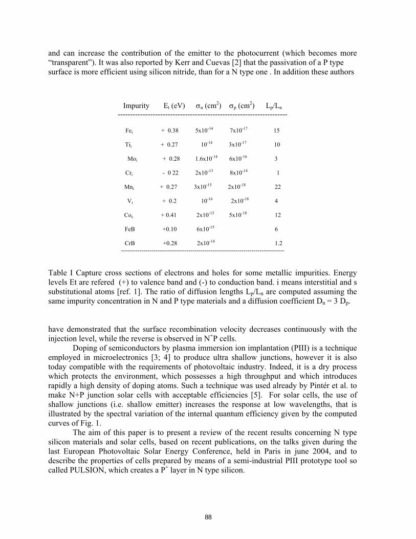
and can increase the contribution of the emitter to the photocurrent (which becomes more “transparent”). It was also reported by Kerr and Cuevas [2] that the passivation of a P type surface is more efficient using silicon nitride, than for a N type one . In addition these authors
Impurity Et (eV) σn (cm2) σp (cm2) Lp/Ln --------------------------------------------------------------------
Fei + 0.38 5x10-14 7x10-17 15
Tii + 0.27 10-14 3x10-17 10
Moi + 0.28 1.6x10⁻¹⁴ 6x10-16 3
Cri - 0 22 2x10-13 8x10-14 1
Mni + 0.27 3x10-15 2x10-18 22
Vi + 0.2 10-16 2x10-18 4
Cos + 0.41 2x10-15 5x10-18 12
FeB +0.10 6x10-15 6
CrB +0.28 2x10-14 1.2
-------------------------------------------------------------------------------- Table I Capture cross sections of electrons and holes for some metallic impurities. Energy levels Et are refered (+) to valence band and (-) to conduction band. i means interstitial and s substitutional atoms [ref. 1]. The ratio of diffusion lengths Lp/Ln are computed assuming the same impurity concentration in N and P type materials and a diffusion coefficient Dn = 3 Dp. have demonstrated that the surface recombination velocity decreases continuously with the injection level, while the reverse is observed in N+P cells.
Doping of semiconductors by plasma immersion ion implantation (PIII) is a technique employed in microelectronics [3; 4] to produce ultra shallow junctions, however it is also today compatible with the requirements of photovoltaic industry. Indeed, it is a dry process which protects the environment, which possesses a high throughput and which introduces rapidly a high density of doping atoms. Such a technique was used already by Pintér et al. to make N+P junction solar cells with acceptable efficiencies [5]. For solar cells, the use of shallow junctions (i.e. shallow emitter) increases the response at low wavelengths, that is illustrated by the spectral variation of the internal quantum efficiency given by the computed curves of Fig. 1.
The aim of this paper is to present a review of the recent results concerning N type silicon materials and solar cells, based on recent publications, on the talks given during the last European Photovoltaic Solar Energy Conference, held in Paris in june 2004, and to describe the properties of cells prepared by means of a semi-industrial PIII prototype tool so called PULSION, which creates a P+ layer in N type silicon.
88

2 RESULTS CONCERNING N TYPE SILICON MATERIALS AND CELLS. 2-1 Properties of N-type silicon wafers
The main investigations and results were done and obtained recently first by Cuevas et al. [6], then by German academic institutions and industrial partners included in the ASiS R&D action, connected to other European laboratories in the frame of a European research contract so called NESSI. In France a tentative programme was launched the last year and it will be translated to a pilot production plant in Grenoble, in the frame of the so called Sinergie Project supported by the French Agency for Environnement and Energy Management.
300 400 500 600 700 800 900 1000 11000
10
20
30
40
50
60
70
80
90
100
110
120
130
Wem
= 100 nm ; η = 13.4%
Wem
= 300 nm ; η = 12.6%
Inte
rnal
Qua
ntum
Effi
cien
cy (
% )
wavelength ( nm )
Fig. 1 Computed variations of the internal quantum efficiency as a function of the emitter thickness.
It was first published [6] that N-type multicrystalline silicon ingots prepared by means
of directional solidification by Eurosolare-Italy (today Enitechnologie) exhibit very large lifetime of minority carriers about 100 µs in raw wafers to few ms in wafers submitted to external gettering by phosphorus diffusion at 880 °C for 1h. The effective lifetime as a function of the excess carrier density in ungettered wafers shows strong trapping at carrier densities below 1015 cm-3. These trapping effects, which are frequently associated with the presence of metallic impurities, disappear with the gettering treatment. The lifetime increases by a factor of 10 for 0.36 Ωcm wafers and by a factor of 50 for 0.9 Ωcm wafer and remains practically constant over a broad range of injection levels. The higher lifetimes appear to be limited by Auger recombination. The minority carrier lifetimes for the N type mc-silicon of various resisitivities are truly exceptional, reaching values which can be found in N-type monocrystalline silicon wafers. In the frame of the ASiS project 11 academic partners (like Fraunhofer Institut für Solar Energie- Freiburg, Max-Planck Institut für Mikrostrukturphysic, Universität Konstanz,
89

etc) and 3 industrial partners ( RWE Schott Solar, Deutsche Solar and Shell Solar) are associated for material supplying, cell fabrication and characterisations [7]. N-type mc-Si casted by Deutsche Solar was characterized before and after improvement steps by J. Libal et al. [8]. In agreement with reference 7 these authors have found very high effective lifetime τp, around 100µs. Then they have submitted wafers to external gettering treatments like phosphorus diffusion and Aluminium – silicon backside alloying. Hydrogenation by means of silicon nitride deposition was also used to passivate the front surface bulk defects . Such passivation has a complementary improvement effect, as reported previously by Périchaud and Martinuzzi [9; 10], who have proposed that hydrogen neutralizes impurities which have not been gettered or which cannot be gettered due to their low diffusion coefficient. After H passivation τp increases up to 140 µs and achieves 200 to 220 µs after gettering, as shown by table II. ---------------------------------------------------------------------------------------------------------------- As-cut H passivation P gettering P gettering Al gettering + Hpassivation ---------------------------------------------------------------------------------------------------------------- τp (µs) 100 140 200 220 220 --------------------------------------------------------------------------------------------------------------- Table II: Measured lifetime at low injection level after different gettering and passivation steps (from ref. 8) applied to 7x10 cm2 wafers. It is clear that the material is very sensitive to gettering treatments, especially to Al-Si alloying which is well reputed to getter metallic impurities. Such a sensitivity is probably more related to the low capture cross sections of impurities in the N-type material rather than to a particular reaction of the material itself during the gettering. (The same amount of remaining impurities has a lower deleterious effect in N-type than in P-type silicon).
C. Schmiga et al. [11] have also found in cast silicon10x10 cm2 area averaged lifetime values about 200 µs. Like in [6] the lifetime does not depend on the injection level over a wide range of the excess carrier densities. Mapping s of P-gettered and H-passivated 6x6 cm2 wafers show that good areas are enlarged and that areas with low initial lifetime are drastically improved: the area averaged value is about 700 µs and the homogeneity is exceptional. These authors have also investigated the behaviour of N-type EFG silicon ribbons 10x10 cm2 and found values around 40 µs, while generally 2 to 5 µs have been measured in p-type wafers. Gettering and hydrogenation increase the high initial lifetime values up to 400 µs, however low lifetime regions are not or only slightly improved. 2-2 Solar cells made with N-type silicon The high diffusion length of minority carriers and the sensitivity of N-type materials to gettering and passivation, especially to the gettering by aluminium-silicon alloying suggest the use of backside junction solar cells which the front surface can be passivated by a slight phosphorus diffusion, as proposed by O. Palais et al. [12]. That does not preclude the use of a hydrogen rich silicon nitride layer to complete the passivations and to realize an antireflection coating. A sketch of the structure is shown by Fig. 2. Such cells were prepared with
90
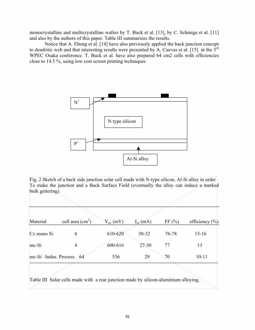
monocrystalline and multicrystalline wafers by T. Buck et al. [13], by C. Schmiga et al. [11] and also by the authors of this paper. Table III summarizes the results.
Notice that A. Ebong et al. [14] have also previously applied the back junction concept to dendritic web and that interesting results were presented by A. Cuevas et al. [15] at the 3rd WPEC Osaka conference. T. Buck et al. have also prepared 64 cm2 cells with efficiencies close to 14.5 %, using low cost screen printing techniques
Fig. 2 Sketch of a back side junction solar cell made with N-type silicon, Al-Si alloy in order To make the junction and a Back Surface Field (eventually the alloy can induce a marked bulk gettering).
Material cell area (cm2) Voc (mV) Jsc (mA) FF (%) efficiency (%) Cz mono Si 4 610-620 30-32 76-78 15-16 mc-Si 4 600-616 27-30 77 13 mc-Si –Indus. Process. 64 536 29 70 10-11 ----------------------------------------------------------------------------------------------------------------- Table III Solar cells made with a rear junction made by silicon-aluminium alloying.
N type silicon
Al-Si alloy
N+
P+
91

Notice that T. Buck et al. have also prepared 64 cm2 cells with efficiencies close to 14.5 %, using low cost screen printing techniques and that C.J.J. Tool has employed industrial processing techniques to make 64 cm2 cells [16] wich the efficiency is close to 11 %. Obviously a key factor for such backside junction cells is the thickness of the wafer which must be as low as possible, provided the front surface is well passivated. Glunz et al. [17] have obtained 19.5 % with 10 Ωcm N-type monocrystalline silicon, 250 µm thick using the laser-fired contact technique which open the way to the combination of a very efficient rear surface passivation and of a P+ BSF due to local diffusion of aluminium. 3 RESULTS RELATED TO THE USE OF PLASMA IMMERSION ION IMPLANTATION DOPING
3-1 Experimental In order to prepare solar cells by BF2 PIII doping, (100) CZ N-type wafers were used,
which the resistivity was 0.7 Ωcm and the thickness was 360 µm. The back surface was phophorus diffused at 850 °C for 30 min in order to create a backside N+ layer. The front side P+ region was obtained using the PULSION tool and a BF2 plasma at various energies between 5 and 25 keV. Then the wafers experienced a conventional annealing at 950°C for 30 min. The metallisations were carried out by Ti and Al deposition by the electron beam technique and annealing at 350°C for 30 min. The front surface grid was obtained by photolithography and chemical etching. The P+ layer was characterized by the four point technique in order to evaluate the doping level and to check the conductivity type. Spectral variations of the internal quantum efficiency (IQE) were used to determine the values of the minority carrier diffusion length L. LBIC technique which led to photocurrent and L scan maps is also used to verify the homogeneity of the cells. SIMS analysis determined the doping profile and also the eventual contamination level.
For comparison cells were also prepared by means of the conventional boron ion beam implantation at an energy of 40 keV and at a dose of 5x1014 cm-2.
3-2 Results Implanted surfaces of wafers submitted to plasma and to ion beam implantations were
analyzed by TXRF. Comparable levels of contamination were found for both wafers, although Ti, Cu and Zn levels are slightly higher in PULSION implanted samples. The global contamination level is acceptable for semiconductor applications. Indeed the minority carrier diffusion lengths are higher than 220 µm in the cells
A typical SIMS profile is given by Fig. 3, before and after annealing. It shows that the junction depth is around 0.12 µm. The four point probe technique confirms that the front layer is P-type and the same tool confirms that the majority of the implanted boron atoms is activated, i.e. the concentration is around 2x1020 cm-3. The LBIC scan map obtained with white light, shows that the photocurrent is homogeneous, indicating that the junction prepared by PIII technique is also homogeneous. The spectral variation of IQE is given by Fig.4 , and is compared with that of a conventional N+P solar cell prepared by phosphorus diffusion. Due to the shallow emitter formed by PIII doping, the response at wavelengths below 600 nm is neatly improved.
92

These experimental results are in agreement with the computed variations of IQE, given by Fig. 1.
With 2x2 cm2 solar cells we obtain Vco = 580 ± 10 mV, Icc = 30 ± 2 mA and conversion efficiencies of 12- 13 %, without antireflection coating.
0.000 0.025 0.050 0.075 0.100 0.125 0.150 0.175 0.2001E14
1E15
1E16
1E17
1E18
1E19
1E20
1E21
1E22
1E23
before annealing after annealing at 950°C/30min
Boro
n co
ncen
tratio
n (c
m-3)
Depth (µm)
Fig. 3 SIMS profile of boron concentration in the samples before and after annealing at 900 °C for 30 min.
400 500 600 700 800 900 1000 1100
0.0
0.2
0.4
0.6
0.8
1.0
Cz BF3 plasma 5 kV Cz BF3 plasma 15 kV diffused Cz solar cell
Nor
mal
ized
Inte
rnal
Qua
ntum
Effi
cien
cy
wavelength (nm) Fig. 4 Experimental spectral variations of IQE for various plasma voltages compared to that
of a conventional solar cell.
Similar results have been obtained with cells prepared by means of conventional boron ion beam implantations. However, the minority carrier diffusion length are higher than in PIII
93
treated cells, suggesting that some contamination can occur during the plasma immersion due to the lack of mass filter. 4 CONCLUSIONS It was demonstrated that N-type silicon, in form of monocrystals or of multicrystals is a very promising material for solar cells, due to low capture cross sections of deep levels associated to metallic impurities for minority carriers. Rear junction cells can be made with such material which the conversion efficiencies are close to 16 % for laboratory cells and 11 % for cells realised by means of industrial process. Plasma immersion ion implantation appears to be a fast technique well suited for photovoltaic production as it is a dry process which can creates highly doped shallow junctions and back or front surface fields. Solar cells with 12-13 % conversion efficiency are easily obtained and will be improved by front surface texturisation. AKNOWLEDGEMENTS The authors would like to thank the French Agency for Environnement and Energy Management and CNRS-ECODEV – France, who have supported TECSEN Laboratory REFERENCES [1] K. Graff, Metal Impurities in Silicon Device Fabrication, Springer Series in Materials, 24, Berlin, 2000 [2] M. Kerr, P. Campbell, A. Cuevas, Proc. of 29th IEEE Photovoltaic Specialists Conf., New Orleans, 2002, p. 438 [3] P.K. Chu, Plasma Physics, Control Fusion, 2003, 555 [4] S. B. Felch et al., Surfaces and Coating Technologies 156, 2002, 229 [5] I. Pintér et al. Proc. of 16th European Photovoltaic Solar Energy Conf., Glasgow, 2000, p.1743 [6] A. Cuevas, M.J. Kerr, C. Schmundsett, F. Ferrazza and C. Coletti, Appl. Phys. Lett., 81,2002,4952 [7] D. Karg, K. Roy, W. Koch, Proc. of 19th European Photovoltaic Solar Energy Conf., Paris june 2004 (to be published) [8] J. Libal et al. in ref. 7 [9] I. Périchaud, M. Stemmer, S. Martinuzzi, J. de Phys IV, C6, 1991, 199 [10] S. Martinuzzi, I. Périchaud, S. De Wolf, F. Warchol, in ref 2, p 170 [11] C. Schmiga et al. in ref. 7 [12] O. Palais, A. Arcari, J. of Appl. Phys., 93, 8, 2003, 4686 [13] T. Buck et al. in ref. 7 [14] A. Ebong et al. NREL Workshop Proc. 2000, 234 [15] A. Cuevas et al., Proc. of 3rd WCPEC, Osaka, 2003 [16] C.J.J. Tool et al. in ref. 7 [17] S. W. Glunz et al. in ref. 7
94
Subsequent Progress on Ga-doped Multicrystalline Silicon Materials and Solar Cells
T. Saitoh, M. Dhamrin, K. Kamisako, T. Eguchi1, T. Hirasawa1 and I. Yamaga1
Tokyo University of Agriculture and Technology Koganei, Tokyo 184-8588, Japan
1Dai-ichi Dentsu Co. Chofu, Tokyo 182-0034, Japan
[email protected] Abstract Sine 1996, photovoltaic market has been growing very rapidly for residential applications mainly in Japan and Germany. To deploy the substantial market, about 30 years were needed since early R&D’s for solar cells due to the first oil crisis in 1973 [1]. Multicrystalline silicon solar cells share more than 60% of the market where the use of multicrystalline cast silicon wafers is relatively cost-effective way if compared with other silicon ingot processes. Due to the shortage of silicon feedstock, better-quality multicrystalline cast silicon ingots are required to realize higher conversion efficiencies. In conventional B-doped multicrystalline silicon wafers, light-induced lifetime degradation [2-4] and other boron related defects including the iron-boron pairs, are the main obstacles to realize highly efficient solar cells. The use of gallium as a dopant in multicrystalline cast silicon wafers has been proven to suppress the light-induced degradation (LID) of carrier lifetimes [5]. In addition, the Ga-doped multicrystalline cast silicon wafers insured almost the same high carrier lifetimes [6] and showed similar cell efficiencies [7] if compared with B-doped multicrystalline cast silicon wafers.
In this research, high-quality Ga-doped ingots were grown in different casting furnaces at the best optimized growing parameters. The 3.5 kg ingots exhibited Gaussian distribution for its diffusion lengths along its height with very high diffusion lengths at the center of the ingot. A high minority-carrier lifetime close to 1 ms was realized in 10Ω·cm Ga-doped wafers after proper P-diffusion and hydrogen passivation. Average minority carrier lifetimes above 400 µs were also realized after P-diffusion and hydrogen passivation for Ga-doped wafers cut from the 70 kg ingot where the response to P-diffusion and hydrogen passivation was pronounced. Using the Ga-doped mc-Si wafers as well as B-doped ones, large-area solar cells with a cell area of 233 cm2 were fabricated. The cell process included reactive-ion texture etching, P-emitter diffusion, junction separation, SiN AR plasma coating, Al-Ag rear and Ag front screen printing. The cell results of Jsc, Voc and cell efficiency for both the cells were plotted as a function of solidified fraction. A small decrease in Jsc and almost no decrease in Voc with the fraction solidified are peculiar irrespective of a great variation of the resistivity in the Ga-doped Si solar cells. This is due to the very high quality nature of the Ga-doped Si wafers reported in the former paper [8]. As a result, cell efficiencies of both the Ga and B-doped mc-Si solar cells showed very similar variation with fraction solidified in the ingots. The other point is that the cell efficiency tended to decrease slightly with position, which is different from the diffusion length distribution in the as-grown mc-Si ingot. The result also suggests that the gettering ability is very high in the Ga-doped mc-Si ingots.
95

Acknowledgement We would like to appreciate Mrs. K. Fukui and K. Shirasawa of Kyocera Corp. for fabricating mc-Si solar cells, Dr. F. Aratani and Mr. T. Nishimura of New Energy and Industrial Technology Development Organization (NEDO) for their technical coordination. This work was financially supported by NEDO as a part of the technology transfer to industry project. References 1. T. Saitoh, “30 Years of Progress in Crystalline Silicon Solar Cells”, presented at 3rd World
Conference on Photovoltaic Energy Conversion, Osaka, May 2003 2. H. Nagel, J. Schmidt, A. G. Aberle and R. Hezel, Proc. of the 14th European Photovoltaic
Solar Energy Conference,1997, 762-765. 3. M. Dhamrin, H. Hashigami and T. Saitoh, “Light-Induced Lifetime Degradation of
Commercial Multicrystalline Silicon Wafers”, Proc. of the 29th IEEE Photovoltaic Specialist Conference. May 2002, 395-398.
4. Y. Kayamori, H. Hashigami, M. Dhamrin and T. Saitoh, “Effect of Illumination Spectra on Light-induced Degradation in Multicrystalline Si Solar Cells”, presented at Proc. of 3rd World Conference on Photovoltaic Energy Conversion, May 2003
5. M. Dhamrin and T. Saitoh, “A Feasibility Study on Gallium Doping for Higher Quality Multicrystalline Silicon Cast Wafers”, Extended Abstract of 12th Workshop on Crystalline Silicon Solar Cell Materials and Processes (2002), 72-79
6. M. Dhamrin, H. Hashigami and T. Saitoh, “Elimination of Light-Induced Degradation with Gallium-doped Multicrystalline Silicon Wafers”, Progress in Photovoltaics 11(4) 231-236 (2003).
7. K. Fukui, S. Fujii, M. Tsuchida, S. Tanimoto, K. Shirasawa, M. Dhamrin and T. Saitoh, “Present Status and Prospects of Ga-doped mc-Si Solar Cells”, presented at 14th Workshop of Crystalline Silicon Solar Cells and Processes, August 2003.
8. M. Dhamrin, H. Hashigami, K. Kamisako, T. Saitoh, T. Eguchi, T. Hirasawa and I. Yamaga, “Extra-Exceptional High Carrier Lifetimes in Ga-doped mc-Si Wafers Toward Millisecond Range”, 19th European Photovoltaic Solar Energy Conference and Exhibition, June 2004
Recent Results on Ga-doped Multicrystalline Silicon Materials and Solar Cells
M. Dhamrin, K. Kamisako and T. SaitohTokyo University of Agriculture and Technology
andT. Eguchi, T. Hirasawa and I. Yamaga
Dai-ichi Dentsu Co.
Silicon Workshop 2004
AcknowledgementsWe would appreciate Mrs. K. Fukui and K. Shirasawa of Kyocera Corp. for fabrication mc-Si solar cells, Dr. F. Aratani and Mr. T. Nishimura of New Energy and Industrial Technology Development Organization (NEDO) for their technical coordination. This work was financially supported by NEDO as a part of the technology transfer to industry project.
Outline of this presentation
• Why Ga-doped mc-Si wafers?• Ingot growth processes. • P-gettering and hydrogen passivation.
3.5 kg ingot75 kg ingot
• Fabrication of solar cells using RIE process• Conclusion
TUAT
96
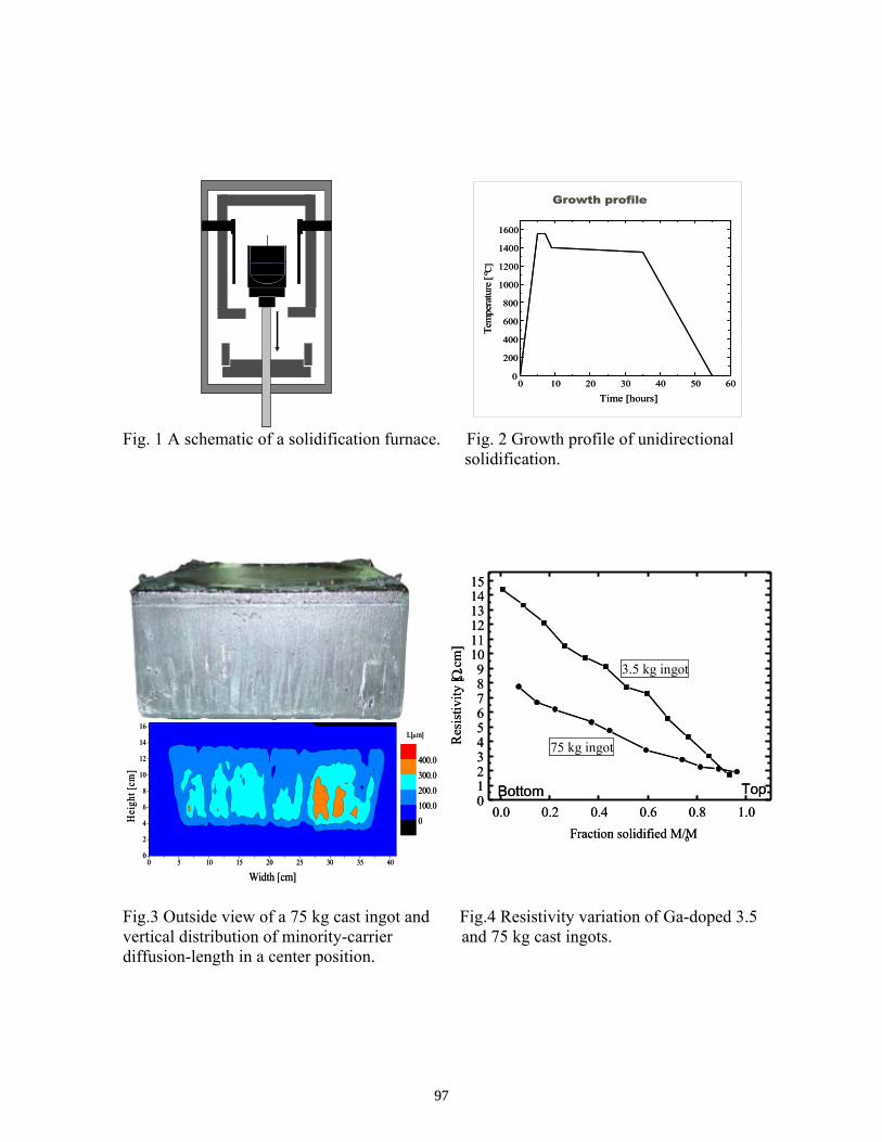
Fig. 1 A schematic of a solidification furnace. Fig. 2 Growth profile of unidirectional solidification. Fig.3 Outside view of a 75 kg cast ingot and Fig.4 Resistivity variation of Ga-doped 3.5 vertical distribution of minority-carrier and 75 kg cast ingots. diffusion-length in a center position.
Growth profile
0 10 20 30 40 50 600
200
400
600
800
1000
1200
1400
1600
Tem
pera
ture
[o C
]
Time [hours]0 10 20 30 40 50 60
0
200
400
600
800
1000
1200
1400
1600
Tem
pera
ture
[o C
]
Time [hours]
0.0 0.2 0.4 0.6 0.8 1.00123456789
101112131415
75 kg ingot
Bottom
Res
istiv
ity [ Ω
.cm
]
Fraction solidified M/M0
Top
3.5 kg ingot
0.0 0.2 0.4 0.6 0.8 1.00123456789
101112131415
75 kg ingot
Bottom
Res
istiv
ity [ Ω
.cm
]
Fraction solidified M/M0
Top
3.5 kg ingot
0 5 10 15 20 25 30 35 400
2
4
6
8
10
12
14
16
Width [cm]
Hei
ght [
cm]
0100.0200.0300.0400.0
L[µm]
0 5 10 15 20 25 30 35 400
2
4
6
8
10
12
14
16
Width [cm]
Hei
ght [
cm]
0100.0200.0300.0400.0
L[µm]
3.5 kg charge3.5 kg charge
97

Fig.5 Phosphorus gettering process sequence Fig. 6 Effect of P-gettering on minority- using PSG diffusion source. carrier lifetimes for small-size Si wafers. Fig. 7 Effects of P-gettering and hydrogen passi- Fig.8 Lifetime map of Ga-doped cast Si vation on average and maximum lifetimes. wafer after P-gettering and H-passivation.
0 50 100 150 200 250
0
200
400
600
800
1000
N2+O2
Tem
pera
ture
[ oC
]
Time [min]
O2
0 50 100 150 200 250
0
200
400
600
800
1000
N2+O2
Tem
pera
ture
[ oC
]Te
mpe
ratu
re [ o
C]
Time [min]
O2
0.0 0.2 0.4 0.6 0.8 1.0
0
50
100
150
Fraction solidified M/M0
Top
As-grown
After P-diffusion
Car
rier l
ifetim
e [ µ
s]
Bottom0.0 0.2 0.4 0.6 0.8 1.0
0
50
100
150
Fraction solidified M/M0
Top
As-grown
After P-diffusion
Car
rier l
ifetim
e [ µ
s]
Bottom
0 5 10 15 20 25 300
5
10
15
20
25
30
[mm]
[mm
]
0100.0200.0300.0400.0500.0600.0700.0
Carrier lifetime [µs]
0 5 10 15 20 25 300
5
10
15
20
25
30
[mm]
[mm
]
0100.0200.0300.0400.0500.0600.0700.0
Carrier lifetime [µs]
40 50
As-grownAfter P-diffusionAfter H-passivation
40 500
50
100
150
200
250
0
50
100
150
200
250
60 7060 70
Max 586µsMax 907µs
Max 593µsMax 231µs
Car
rier l
ifetim
e [µ
s]
Wafer number
As-grownAfter P-diffusionAfter H-passivation
40 50
As-grownAfter P-diffusionAfter H-passivation
40 500
50
100
150
200
250
0
50
100
150
200
250
60 7060 70
Max 586µsMax 907µs
Max 593µsMax 231µs
Car
rier l
ifetim
e [µ
s]
Wafer number
As-grownAfter P-diffusionAfter H-passivation
98

Fig.9 Effect of P-diffusion and hydrogen passi- Fig.10 QSSPC data of cast Si wafers before vation on carrier-lifetime variation with the and after P-gettering and H-passivation of position of the 75 kg Ga-doped mc-Si ingot. the center of the 75 kg ingot. Fig.11 Kyocera cell fabrication process Fig.12 Short-circuit current density of Ga and using RIE texture. B-doped cast Si cells along vertical positions.
0.0 0.2 0.4 0.6 0.8 1.0
0
50
100
150
200
250
300
350
400
450Bottom
Before gettering
After P-gettering
Car
rier l
ifetim
e [ µs
]
Fraction solidified M/M0
After P-gettering and HP
Top
0.0 0.2 0.4 0.6 0.8 1.0
0
50
100
150
200
250
300
350
400
450Bottom
Before gettering
After P-gettering
Car
rier l
ifetim
e [ µs
]
Fraction solidified M/M0
After P-gettering and HP
Top
1E12 1E13 1E14 1E15 1E16
100
After P-diffusion & HP
4.75 Ω.cm
Before GetteringCar
rier l
ifetim
e [µ
s]
Excess carrier concentration [cm-3]
400
201E12 1E13 1E14 1E15 1E16
100
1E12 1E13 1E14 1E15 1E16
100
After P-diffusion & HP
4.75 Ω.cm
Before GetteringCar
rier l
ifetim
e [µ
s]
Excess carrier concentration [cm-3]
400
20
0.0 0.2 0.4 0.6 0.8 1.0
31
32
33
34
35
J sc[m
A/c
m2 ]
Fraction solidified M/M0
Ga-doped
B-doped
0.0 0.2 0.4 0.6 0.8 1.0
31
32
33
34
35
J sc[m
A/c
m2 ]
Fraction solidified M/M0
Ga-doped
B-doped
RIE texturing
P diffusion
Parasitic junction removal
PECVD SiN deposition (front)
Front Ag and back Al/Ag
Contact by printing
99
Fig.13 Open-circuit voltage of Ga and B-doped Fig.14 Comparison between Ga and B- mc-Si solar cells along vertical positions. doping on cell efficiency variation with vertical positions.
0.0 0.2 0.4 0.6 0.8 1.0
0.55
0.56
0.57
0.58
0.59
0.60
0.61
0.62
Voc
[vol
t]
Fraction solidified M/M0
Ga-doped
B-doped
0.0 0.2 0.4 0.6 0.8 1.0
0.55
0.56
0.57
0.58
0.59
0.60
0.61
0.62
Voc
[vol
t]
Fraction solidified M/M0Fraction solidified M/M0
Ga-doped
B-doped
0.0 0.2 0.4 0.6 0.8 1.0
13
14
15
16
E ff[
%]
Fraction solidified M/M0
Ga-doped
B-doped
0.0 0.2 0.4 0.6 0.8 1.0
13
14
15
16
E ff[
%]
Fraction solidified M/M0
Ga-doped
B-doped
Conclusions
• Average carrier lifetimes over 400 µs were realized on 4.7 Ω·cm, Ga-doped mc-Si wafers by P-diffusion and hydrogen passivation.
• A possibility to achieve a lifetome as high as 1 ms was indicated in 10 Ω ·cm mc-Si wafer.
• 16% -efficient, large-area mc-Si solar cells were fabricated for both the Ga and B-doped Si wafers by RIE process.
• Irrespective of great change in resistivity, cell efficiencies tended to decrease very slightly with fraction solidified for Ga-doped Si wafers, indicating that the quality was very high.
100

Generation Mechanism of LID in B-Doped CZ-Si using Molecular Orbital Method
Yoshio Ohshita, Tuong Khanh Vu, and Masafumi Yamaguchi Toyota Technological Institute, 2- 12- 1 Hisakata, Tempaku, Nagoya 468-85 1 1 Japan
Tel: +8 1-52-809- 1 876, E-mail: [email protected]
ABSTRACT
The defects were induced in the B -doped CZ - Si by the light irradiation and/or minority carrier injection. They acted as a recombination center and degraded the cell performances. The induced defect was unstable and was annihilated by 200°C annealing. The total numbers of induced defects were determined by the difference between the defect generation and annihilation reaction rates. Analyzing the Voc change due to the electron injection indicated that the defect was positively charged and that its energy level was 0.26 eV, which corresponded to the interstitial B - interstitial 0 complex. Since the number of induced defects was too small for the experimental analysis, mechanism of this defect generation was theoretically studied by ab inito molecular orbital calculations with cluster system. When there was an 0 2 molecule near the substitutional €3, there was no attractive force and no chemical bond was created between them. On the other hand, when the diffusion process of interstitial Si atom was enhanced by the light irradiation or minority carrier injection, the interstitial B was generated by the kick-out process and that the interstitial B - interstitial 0 complex was generated. Mulliken population analysis indicated that this defect was positively charged. The defect generated a deep energy level, suggesting that it efficiently would trap the minority carrier electrons and act as a recombination center.
1. Introduction
Boron (B) doped Czochralski (CZ) - grown silicon (Si) wafer is widely used as a solar cell material, because it is relatively low-cost and conversion efficiencies well above 20% can be achieved. However, the initial cell efficiency is degraded by defects that are created by light irradiation and/or minority carrier injection [ 1-41 These defects act as recombination centers and shorten the minority carrier (electron) lifetime, resulting in the degraded solar cell performance. Therefore, suppressing this degradation is one of the most important problems to solve to fabricate high - quality and low - cost Si solar cells.
Wafers of CZ - Si have a large amount of interstitial oxygen (0) cm3). They are intentionally doped for the intrinsic gettering (IG) process, which is required for fabricating ultra large - scale integration (ULSI) circuits having good electrical properties. When the 0 concentration in the CZ-Si is high, light irradiation and/or minority carrier injection severely degrade cell performances [2]. This degradation does not occur when floating zone (FZ) Si, which contains a small amount of 0 in the Si crystal is used as the solar cell material [2]. Thus, we can conclude that the interstitial 0 plays a role inducing the defect. This degradation is not observed for substrates with low B and high 0 concentrations. The number of induced defects linearly increases as the €3
101

concentration increases, when the 0 concentration is constant. For another example, when gallium (Ga) is used as an impurity for p-type conductivity, there is no degradation even in highly Ga- and 0- doped CZ-Si [S]. These facts suggest that the defect induced by the light irradiation / carrier injection is composed of both B and 0, and that the B - 0 complex plays a key role in the degradation of solar cell performance. This defect is annihilated by 200°C thermal annealing and the solar cell performance can be recovered, indicating that the defect is not very stable. To explain the role of these B and 0 related phenomena in the degradation of the solar cell performances, several models, such as the interstitial B and interstitial 0 defect complex, have been proposed. However, the unstable atomic structure of the defect induced by the light illumination and/or minority carrier injection, is not clear yet.
In this paper, the mechanism of defect generation induced by the light irradiation or minority carrier injection was studied by using both experimental techniques and ab initio molecular orbital calculations.
2. Experiment
The number of defects (NT) induced by minority carrier injection was estimated based on the decrease in open - circuit voltage (V0J of solar cells by using the following equations. voc = (kT/o-o, , &) (1)
A[l/ exp(V,, )I2 c€ A(11 L n ) (2)
(3) N, = U(T,,OV~,J Here, k, T, q are Boltzman constant, absolute temperature, and electronic charge. I,, and I0 are the short - circuit current, and diode saturation current. Ln,
T ~ , 0 , Yth are diffusion length, minority carrier lifetime, capture cross-section, and thermal velocity of minority carrier. The defect concentration induced by minority carrier injection is shown in Fig. 1, as functions of injection time and substrate temperature. The defect concentration increases as the injection time and then becomes saturated. When the substrate temperature is higher during the current injection, the concentration increases more quickly and the saturated value of the defect concentration increases.
6
25 50 75 Injection time fmin>
Fig. 1 Relationship between the induced defect concentration and the injection time as a function of the substrate temperature during the injection.
The induced defects were unstable and these number decreased by the thermal annealing as shown in Fig. 2. When the annealing temperature was higher, the defect concentration decreased more quickly and the defects were annihilated by 200°C annealing (20 min). While the 150°C annealing decreased the defect concentration, the large amounts of defects were induced at the same temperature by the minority carrier injection as shown in Fig. 1. This result indicated that both the generation and annihilation processes happened during
102
the injection process, and that the total number of induced defects was determined by the difference between these reaction rates.
- 0 5 10 1s 20 Annealing Time (min)
Fig. 2 Relationship between the defect concentration and annealing time, as a function of the annealing temperature.
To determine the energy level of the induced defect, the temperature dependence of the difference between the initial lifetime and the lifetime decreased by the electron injection was studied. The relationship between the lifetime change and measuring temperature is shown in Fig. 3. When the temperature was lower than 200K, the lifetime was almost constant. Since all electrons trapped by the defect recombined with holes, there was no temperature dependence. On the other hand, as increasing the temperature, the lifetime - difference increased. This means that at higher temperatures, some of electrons captured by the defect were thermally released and did not recombine with holes. Therefore, the energy level of defect could be estimated by using the following equation.
Here, and C2 are constants. The estimated energy level was about 0.26 eV from the conduction band, which corresponds to that of interstitial B and interstitial 0 complex. Moreover, since the lifetime change should be constant at lower temperatures, it was suggested that the capture cross-section would have a temperature dependence T-3’2, and that the defect might be positively charged and efficiently capture minority carrier electrons.
Temperature (K) 400 300 200 100
1 0 - ’ 4 C J
Fig, 3 Relationship between the lifetime change and substrate temperature,
3. Calculations
To clarify the structure of the B and 0 related defect complex, ab initio calculations were carried out using the cluster model. The schematic illustration of the cluster used is shown in Fig. 4. It consists of 28 or 29 Si, one interstitial or substitutional B, one interstitial 0 or 02, and 36 hydrogen atoms. Hydrogen atoms were introduced to terminate the unpaired electrons of the outside Si atoms in the cluster. The total energy of the cluster was calculated. The calculations were performed according to the density function theory (DFT), and the three parameter Becke-Lee-Yang-Parr hybrid
103

(B3LYP) implementation of DFT was adopted [8]. The effective core potential LANL2DZ was used as a basis set [9]. An ab inito calculation program, GAUSSIAN 98, was used for all the calculations. Images of the molecular structures and molecular orbitals were obtained by using GAUSS-VIEW. A Mulliken population analysis was carried out to estimate the number of electrons in the B, Si, and 0 atoms, respectively. The electronic level of the defect complex was obtained by D V - X a calculations [ l o ] and the electrical character of the defect was studied.
cell performance. To clarify the 0 2 effect on the generation of the B - 0 complex, ab initio molecular orbital calculations were carried out using a cluster model. The shapes of the highest occupied molecular orbital (HOMO) and the lowest unoccupied molecular orbital (LUMO) of the cluster system are shown in Fig 5. The electron distributions of B and 0 in HOMO indicated that there was no chemical bond formed between them. LUMO was not composed of B and 0 atomic orbitals too. These results suggested that there was not attractive force between B and 0 2 in the Si crystal.
Fig. 4 Schematic illustration of the used cluster system.
4. Results and discussion
Several models about B and 0 related defects were proposed. In this work, we studied the 0 2 diffusion model and the interstitial B - interstitial 0 one.
4-1 0 7 diffusion model Recently, the following 0 2 model was
proposed [l l] . 0 2 diffusion in the Si
irradiation. During the 0 2 diffusion, 0 2
reacts with the impurity B and make a defect complex, which deteriorates the
...
crystal is enhanced by the light (b)
Fig. 5 Images of highest occupied (a) and lowest unoccupied (b) molecular orbitals.
104

Therefore, when the 0 2 diffuses in the Si crystal and comes near the interstitial B, the defect complex composed of 0 2 and B is not created. The stable spin state of 0 2
is triplet, while that of B in the Si crystal is singlet as shown in Table 1. This may be the reason why they cannot make a stable bond between them. If 0 2 is decomposed near the substitutional B, oxygen atom is a radical and it will create the fairly stable chemical bond with B. However, This cannot explain that the defect induced by the light irradiation is unstable and that it is annihilated by the relative 1 y low temperature annealing (200°C). Moreover, the oxygen dimmer can diffuse in the Si crystal above 450°C. This result also indicates that B-02 complex cannot be decomposed at 200°C, even if this structure is created.
Table 1 Total Energy (atomic u.)
Singlet -3 04.9 897 Triplet -304.9954
4-2: Interstitial B - interstitial 0 model
The interstitial B and the interstitial 0 defect complex model have been proposed. However, the unstable atomic structure of the defect induced by the light illumination and/or minority carrier injection is not clear yet. Therefore, to determine the structure of the interstitial B and the interstitial 0 related defect, the total energy of the duster was calculated as a function of the position of the interstitial B. The relationship between the total energy and the distance of the interstitial B from the interstitial 0 is shown in Fig. 6. The total energy monotonically decreases as the distance of B from 0 increases, indicating that
0.0 0.5 1.0 1.5 2.0 2.5
Distrtncc of I3 from 0 (A)
Fig. 6 Potential curve of cluster system as a function of the distance of interstitial B from interstitial 0.
there is no attraction between these interstitial atoms. The shape of the highest occupied molecular orbital (HOMO) is shown in Fig. 7. The distance of B from 0 was about 0.1 nm. The orbitals of B and 0 are out of phase, and the electron distributions of B and 0 indicate that there is no chemical bond formed between them. The two chemical bonds between the interstitial 0 and the substitutional Si atoms are strong. Hence, no chemical bond was produced when the interstitial B approached the interstitial 0,
Fig. 7 Image of highest occupied molecular orbital of the system.
105

indicating that there was only a large electron repulsion force between them. Therefore, the interstitial B did not exist stably near the interstitial 0, and was removed from the neighbor of the 0 that was lowering the total energy. These results suggest that even if a defect complex made of the interstitial B and interstitial 0 is generated by light irradiation, it is easily decomposed and does not affect the minority carrier lifetime during solar cell operation.
The interstitial B exists stably at a position near the substitutional Si as an interstitial B - substitute Si - interstitial 0 complex, as shown in Fig 8. The overlap population analysis suggested that there is a weak chemical bond between the interstitial B and the substitutional Si. It also suggested that the electronic
Y.
Fig. 8 Structure of stable interstitial B - interstitial 0 defect complex.
configuration of the defect was mainly determined by the electrons of the first- and second-neighbor atoms, meaning that the present cluster size was sufficient for discussions of the defect structure. The estimated stabilization energy was about 0.7 eV. Here, the stabilization energies were calculated as the activation energy for the B diffusion to the neighbor stable
Fig. 9 Stabilization energy for the interstitial B - substitutional Si - interstitial 0 complex.
position (Fig. 9). When there is not an interstitial 0 near the interstitial B and substitutional complex, the interstitial B also exists at the same position stably, however, the stabilization energy decreases (Fig. 9). Using the Mulliken population-analysis method, we estimated the electron populations of B, Si, and 0 in the defect complex (Table 2). The Si and B atoms were positively charged and the
l ' a b l c 2 13 si
with 0 4.9 13.2 without 0 5.1 14.1
0 was negatively charged, because the electron affinity of 0 is larger than those of Si and B. This charge flow from Si and B to 0 caused the repulsion energy between the Si and B to decrease. This is the reason why the larger stabilization energy of the interstitial B was obtained due to the existence of the interstitial 0. Therefore, when interstitial B migrates in Si crystal, the interstitial B - substitutional Si - interstitial 0 complex is more easily formed as compared with the interstitial B - substitutional Si pair. However, the stabilization energy is not so large, even though there is an interstitial 0 in the
106
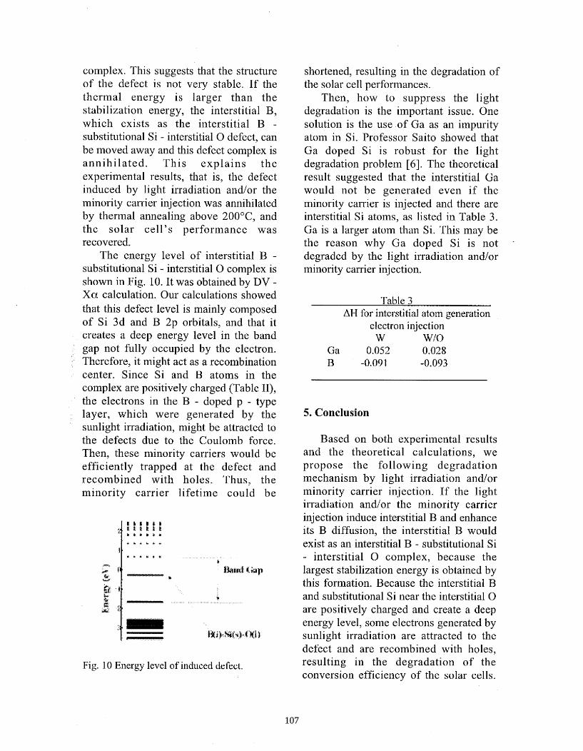
complex. This suggests that the structure of the defect is not very stable. If the thermal energy is larger than the stabilization energy, the interstitial B, which exists as the interstitial B - substitutional Si - interstitial 0 defect, can be moved away and this defect complex is annihilated. This explains the experimental results, that is, the defect induced by light irradiation and/or the minority carrier injection was annihilated by thermal annealing above 2OO0C, and the solar cell's performance was recovered.
The energy level of interstitial B - substitutional Si - interstitial 0 complex is shown in Fig. 10. It was obtained by DV - X a calculation. Our calculations showed that this defect level is mainly composed of Si 3d and B 2p orbitals, and that it creates a deep energy level in the band gap not fully occupied by the electron. Therefore, it might act as a recombination center. Since Si and B atoms in the complex are positively charged (Table 11), the electrons in the B - doped p - type layer, which were generated by the sunlight irradiation, might be attracted to the defects due to the Coulomb force. Then, these minority carriers would be efficiently trapped at the defect and recombined with holes. Thus, the minority carrier lifetime could be
Fig. 10 Energy level of induced defect.
shortened, resulting in the degradation of the solar cell performances.
Then, how to suppress the light degradation is the important issue. One solution is the use of Ga as an impurity atom in Si. Professor Saito showed that Ga doped Si is robust for the light degradation problem [ 61. The theoretical result suggested that the interstitial Ga would not be generated even if the minority carrier is injected and there are interstitial Si atoms, as listed in Table 3 . Ga is a larger atom than Si. This may be the reason why Ga doped Si is not I
degraded by the light irradiation and/or minority carrier injection.
Table 3 AH for interstitial atom generation
e 1. ec t TO n i qj cc t i on M! U'lO
Cia 0.052 0,028 R -0.09 t -0.093
5. Conclusion
Based on both experimental results and the theoretical calculations, we propose the following degradation mechanism by light irradiation and/or minority carrier injection. If the light irradiation and/or the minority carrier injection induce interstitial B and enhance its B diffusion, the interstitial B would exist as an interstitial B - substitutional Si - interstitial 0 complex, because the largest stabilization energy is obtained by this formation. Because the interstitial B and substitutional Si near the interstitial 0 are positively charged and create a deep energy level, some electrons generated by sunlight irradiation are attracted to the defect and are recombined with holes, resulting in the degradation of the conversion efficiency of the solar cells.
107

However, the binding energy of the interstitial B to the substitutional Si is not very large. Therefore, the interstitial B can be removed easily from this site by thermal annealing and the defect complex is annihilated. The interstitial B can be kicked-in to a substitutional site during diffusion, because the kink-in process requires relatively small energy (0.5 eV). Then, there will be few defects that act as recombination centers, and solar cell performance will be recovered. The Ga doped Si is not degraded by the light irradiation. This reason could be explained by the difference between the atom sizes of B and Ga.
REFERENCES
S. W. Glunz, S. Rein, W. Warta, J. Knobloch, and W. Wettling, Proc. of 2nd World Conference on Photovoltaic Solar Energy Conversion, 1998, p. 1343. J. Schmidt and A. Cuevas, J. Appl. Phys. 86(6) 3 175 (1999) S. W. Glunz, S. Rein, W. Warta, J. Knobloch, and W. Wettling, Techin ica l Diges t o f the International PVSEC- 1 I , 1999, p. 549 S. Rein, T. Rehrl, J. Isenberg, W. Warta, and S. W. Glunz, Proc. of 16th European Photovoltaic Solar Energy Conference, 2000. J. Schmidt, A. G. Aberle, and R. Hezel, Proc. of 26th TEEE P ho tovoltaic Specialists Conference, 1997, p. 13. T. Saito, X. Wang, €3. Hashigami, T. Abe, T. Igarashi, S. Glunz, W. Wettling, A. Ebong, B. Damiani, A. Rohatgi, I. Yamasaki, T. Nunoi, H. Sawai, H. Ohtsuka, Y. Yazawa, T. Warabisako, J. Zhao, and M. Green,
Tech. Digest of 1 lth International Pho tovo l t a i c Sc ience a n d Engineering Conference, 1999, p. 553. H. Hashigami, X. Wang, T. Abe and T. Saito, Tech. Digest of l l t h International Photovoltaic Science and Engineering Conference, 1999, p. 978. A. D. Becke, J. Chem. Phys. 98 5648 (1993) T. H. Dunning Jr. and P. J. Hay, in “Modern Theoretical Chemistry”, Ed. H. F. Shaefer, TTI (Plenum, New York, 1976), vol. 3, 1. H. Adachi, M. Tsukada, and C. Satoko, J. Phys. SOC. Jpn., 45 875 (1 978) J.Schmidt, K. Bothe and R. Heze, presented at 29th IEEE PVSEC (2002).
108
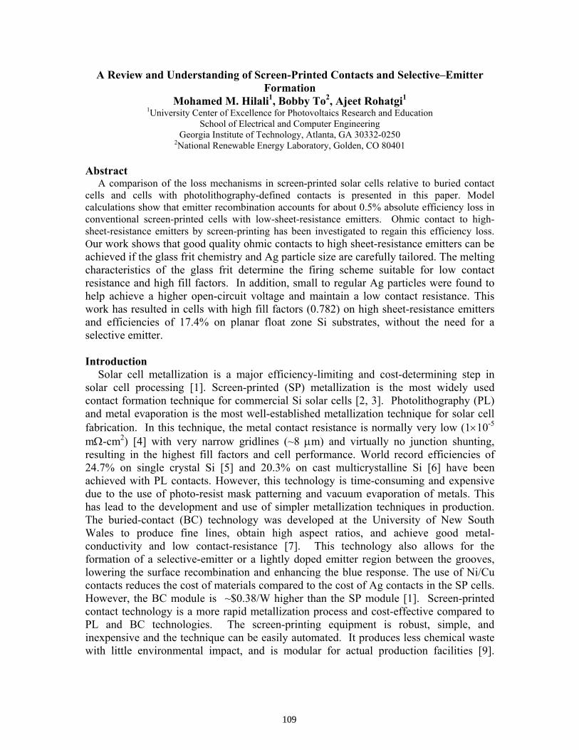
A Review and Understanding of Screen-Printed Contacts and Selective–Emitter Formation
Mohamed M. Hilali1, Bobby To2, Ajeet Rohatgi1 1University Center of Excellence for Photovoltaics Research and Education
School of Electrical and Computer Engineering Georgia Institute of Technology, Atlanta, GA 30332-0250
2National Renewable Energy Laboratory, Golden, CO 80401 Abstract
A comparison of the loss mechanisms in screen-printed solar cells relative to buried contact cells and cells with photolithography-defined contacts is presented in this paper. Model calculations show that emitter recombination accounts for about 0.5% absolute efficiency loss in conventional screen-printed cells with low-sheet-resistance emitters. Ohmic contact to high-sheet-resistance emitters by screen-printing has been investigated to regain this efficiency loss. Our work shows that good quality ohmic contacts to high sheet-resistance emitters can be achieved if the glass frit chemistry and Ag particle size are carefully tailored. The melting characteristics of the glass frit determine the firing scheme suitable for low contact resistance and high fill factors. In addition, small to regular Ag particles were found to help achieve a higher open-circuit voltage and maintain a low contact resistance. This work has resulted in cells with high fill factors (0.782) on high sheet-resistance emitters and efficiencies of 17.4% on planar float zone Si substrates, without the need for a selective emitter. Introduction
Solar cell metallization is a major efficiency-limiting and cost-determining step in solar cell processing [1]. Screen-printed (SP) metallization is the most widely used contact formation technique for commercial Si solar cells [2, 3]. Photolithography (PL) and metal evaporation is the most well-established metallization technique for solar cell fabrication. In this technique, the metal contact resistance is normally very low (1×10⁻⁵ mΩ-cm2) [4] with very narrow gridlines (~8 µm) and virtually no junction shunting, resulting in the highest fill factors and cell performance. World record efficiencies of 24.7% on single crystal Si [5] and 20.3% on cast multicrystalline Si [6] have been achieved with PL contacts. However, this technology is time-consuming and expensive due to the use of photo-resist mask patterning and vacuum evaporation of metals. This has lead to the development and use of simpler metallization techniques in production. The buried-contact (BC) technology was developed at the University of New South Wales to produce fine lines, obtain high aspect ratios, and achieve good metal-conductivity and low contact-resistance [7]. This technology also allows for the formation of a selective-emitter or a lightly doped emitter region between the grooves, lowering the surface recombination and enhancing the blue response. The use of Ni/Cu contacts reduces the cost of materials compared to the cost of Ag contacts in the SP cells. However, the BC module is ~$0.38/W higher than the SP module [1]. Screen-printed contact technology is a more rapid metallization process and cost-effective compared to PL and BC technologies. The screen-printing equipment is robust, simple, and inexpensive and the technique can be easily automated. It produces less chemical waste with little environmental impact, and is modular for actual production facilities [9].
109

Screen-printing is truly a cost-effective option for large-scale solar cell manufacturing provided that high-quality contacts with FF≥0.77 can be achieved in production.
An understanding of the loss mechanisms in screen-printed contacts
Factors that tend to limit the solar cell performance of screen-printed cells are summarized below:
Screen-printed contacts are typically 125-150 µm wide, which gives rise to high shading losses. Fill factors are low (~0.75) because of high contact resistance, low metal
conductivity, and junction shunting. Effective emitter surface passivation is difficult because of the use of low
sheet-resistance emitters with a high surface concentration. This is done to achieve a reasonable contact resistance (≤ 3 mΩ-cm2). This also results in poor short-wavelength response due to heavy doping effects and increased Auger recombination in the emitter region.
Due to the above factors, the efficiency of screen-printed cells is typically 1.5-2% lower than that of cells with photolithography contacts [10]. Model calculations in Fig. 1 show the quantitative breakdown of these losses, which are divided into three categories: contact quality, short-wavelength response, and shading. The pie chart in Fig. 1 shows that contact quality is inferior due to high contact-resistance, low conductivity of the SP Ag gridline, and emitter sheet resistance loss due to wider gridline spacing. The loss in short-wavelength response is caused by a high front-surface recombination velocity and heavy-doping effects in the emitter. Finally, the high shading loss is due to the wide SP gridline and busbar. Table 1 summarizes the key differences in contact parameters and quality of PL, BC, and SP contacts.
P aram eter S P C e ll B C ce ll P L ce llfinger thic kness 14 µm 50 µm 8 µm
finger width 80 µm 20 µm 20 µms pec ific contac t-res is tanc e 0.3-3 m Ω -c m 2 3 µΩ -cm 2 0.01 m Ω −cm 2
m etal res is tivity 3 µΩ -c m 1.7 µΩ -c m 1.7 µΩ -cmFill Fac tor 0.74-0.77 0.78-0.79 0.81-0.82
Table 1: A comparison of SP, BC, and PL front contact metallization techniques.
Fig. 1. Loss mechanisms in SP cells relative to PL cells.
Sheet Loss 0.1% Conductivity
0.2%
Contact Resistance 0.2%
Grid Shading 0.5%
Heavy Doping (Emitter) 0.3% Front Surface
Recombination 0.4%
Contact Quality
Short-Wavelength Response
Reflectance
110

Selective-Emitter Cells The advantages of a selective-emitter cell include a low contact resistance due to
heavy doping underneath the metal grid, improved front-surface passivation of the lightly doped region between the grid, and reduced recombination under the metal contact. In the case of BC cells a selective-emitter is achieved by two-step diffusion with the heavy diffusion only in the grooves. Therefore, the BC cell can be categorized as a selective-emitter cell with plated contacts [11].
In the case of screen-printing, a selective-emitter is difficult to achieve especially by a one-step process. Recently several innovative techniques to form a screen-printed selective-emitter cell have been attempted. These techniques can be divided in three categories: (a) selective-emitter cells fabricated via masking and etching with no alignment [12], (b) selective-emitter cells fabricated by self-alignment without the need for masking or
etching [13], and (c) selective-emitter cells fabricated by self-aligned self-doping Ag pastes [14, 15].
Techniques (a) and (b) are generally time consuming and somewhat expensive. Technique (c) is not trivial because the diffusivity of Ag in Si [16] is higher than that of P [17], which can lead to a high junction leakage current and n factor. To develop screen-printed contacts to high sheet resistance emitters, we first review the current understanding of screen-printed formation. Then we discuss our work on the formation of good SP ohmic contacts to high sheet-resistance emitters. This work has resulted in cells with high fill factors (0.782) and efficiencies of 17.4% on untextured FZ Si substrates, without the need for a selective emitter. A Brief Review of the Current Understanding of the Contact Formation and Current Transport Through Screen Printed Contacts
Screen-printed contact formation and current transport is not fully understood, nevertheless, Ballif et al. [18,19] and Schubert et al. [20-22] have proposed some models based on electrical and physical characterization of screen-printed contacts. The glass frit included in commercial Ag pastes plays a crucial role in contact formation. Lead borosilicate glass frit is commonly used, which etches the antireflection coating, reduces the melting point of Ag, and promotes adhesion to Si during the firing cycle. The reaction between the glass frit and the SiNx layer takes place via a redox reaction [23]. The glass frit also acts as a barrier to Ag diffusion from the paste into the emitter region and p-n junction [24]. This could help in reducing junction shunting and leakage current.
The general understanding is that upon heating the glass frit melts and wets the surface. According to the Pb-Ag phase diagram, the glass frit dissolves Ag and etches the SiNx antireflection coating while the Ag is sintered during firing. When the liquid glass reaches the Si emitter, Si is also dissolved in the lead-silver melt. Upon cooling, Si re-grows epitaxially [18, 25, 26] followed by Ag crystallites at the Si surface. The glass layer then solidifies and Pb precipitates are formed in the glass layer. The Ag crystallites are believed to be isolated metal-semiconductor ohmic contact regions responsible for the current transport from the Si emitter to the Ag grid, and have very low contact resistivity (2×10⁻⁷ Ω-cm2) with the Si emitter [19]. In some cases the Ag crystallites at the Si emitter surface re-crystallize along (111) planes to give an inverted pyramid shape. However, sometimes the Ag crystallites are elongated or form a rounded interface with the Si
111
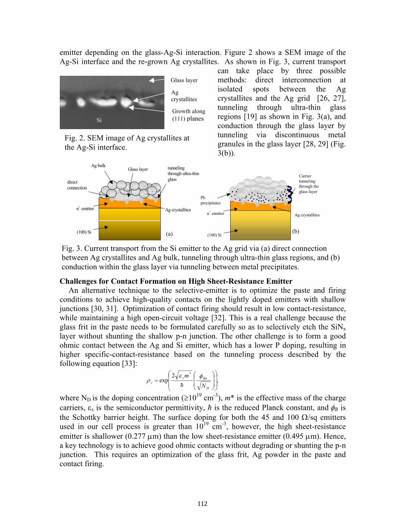
emitter depending on the glass-Ag-Si interaction. Figure 2 shows a SEM image of the Ag-Si interface and the re-grown Ag crystallites. As shown in Fig. 3, current transport
can take place by three possible methods: direct interconnection at isolated spots between the Ag crystallites and the Ag grid [26, 27], tunneling through ultra-thin glass regions [19] as shown in Fig. 3(a), and conduction through the glass layer by tunneling via discontinuous metal granules in the glass layer [28, 29] (Fig. 3(b)).
Challenges for Contact Formation on High Sheet-Resistance Emitter An alternative technique to the selective-emitter is to optimize the paste and firing
conditions to achieve high-quality contacts on the lightly doped emitters with shallow junctions [30, 31]. Optimization of contact firing should result in low contact-resistance, while maintaining a high open-circuit voltage [32]. This is a real challenge because the glass frit in the paste needs to be formulated carefully so as to selectively etch the SiNx layer without shunting the shallow p-n junction. The other challenge is to form a good ohmic contact between the Ag and Si emitter, which has a lower P doping, resulting in higher specific-contact-resistance based on the tunneling process described by the following equation [33]:
where ND is the doping concentration (≥1019 cm-3), m* is the effective mass of the charge carriers, εs is the semiconductor permittivity, ħ is the reduced Planck constant, and φB is the Schottky barrier height. The surface doping for both the 45 and 100 Ω/sq emitters used in our cell process is greater than 1019 cm-3, however, the high sheet-resistance emitter is shallower (0.277 µm) than the low sheet-resistance emitter (0.495 µm). Hence, a key technology is to achieve good ohmic contacts without degrading or shunting the p-n junction. This requires an optimization of the glass frit, Ag powder in the paste and contact firing.
,2
exp*
=
D
Bnsc N
m φερ
(b) (a)
tunnelingthrough ultra-thinglass
(100) Si
n+ emitter Ag crystallites
directconnection
Ag bulkGlass layer
Pbprecipitates
Carriertunnelingthrough theglass layer
(100) Si
n+ emitter Ag crystallites
Fig. 3. Current transport from the Si emitter to the Ag grid via (a) direct connection between Ag crystallites and Ag bulk, tunneling through ultra-thin glass regions, and (b) conduction within the glass layer via tunneling between metal precipitates.
Si
Ag crystallites
Glass layer
Growth along (111) planes
Fig. 2. SEM image of Ag crystallites at the Ag-Si interface.
112

Higher ρc Low ρc
Fig. 5. AFM plane-view images for (a) sparsely distributed, and (b) regularly distributed Ag crystallites after the removal of the Ag and glass frit contact.
(a) (b)
Criteria for the Glass frit Behavior to Achieve High-Quality Contacts to High Sheet-Resistance Emitters
Aggressive glass frit etches more Si and allows the dissolved Ag to penetrate deep into the p-n junction. Excessive penetration of Ag in the emitter region can also occur if the glass layer does not properly act as a barrier to Ag diffusion. Figure 4 shows SIMS Ag profiles in the Si emitter region underneath the Ag gridline for an aggressive glass and a mild glass that is designed to prevent Ag diffusion into the Si emitter. Excessive penetration of Ag into the p-n junction region degrades Voc [34] due to an increase in the junction leakage current (Jo2) [30]. Suns-Voc analysis [35] showed that Jo2 is very high (2,678 nA/cm2) for the aggressive glass frit in Fig. 4, and is lower (15 nA/cm2, n2=2) for the less aggressive glass frit.
To achieve good ohmic contact to a high sheet-resistance emitter without shunting the shallow emitter, the glass frit must not be very aggressive. However, if the glass frit is very mild, it will not etch the SiNx completely for conventional firing temperatures. For example, we have found that inadequate firing of PV168 Ag paste from Dupont led to a very high specific contact-resistance (46 mΩ-cm2). A more aggressive etching reaction between the glass frit and the SiNx was achieved by firing at higher temperatures (>810°C). This caused the SiNx layer to be etched and resulted in Ag crystallite re-growth on the Si emitter surface. As a result, the specific contact-resistance decreased significantly to ≤2 mΩ-cm2.
As reported in [19], a problem in contacting lightly doped emitters is the sparse contact regions (Ag crystallites) between the Si emitter and the Ag grid. Atomic force microscopy (AFM) can be used to obtain a footprint of the distribution of the Ag crystallites at the Ag-Si interface for different Ag pastes. Figure 5 shows AFM plane-view images of two Ag pastes after removal of the Ag and glass frit; one shows (a) sparse
irregular pit distribution and higher ρc ~3 mΩ-cm2 and the other (b) shows a more regular and uniform distribution of pits or inverted pyramids and lower ρc ~0.6 mΩ-cm2. It was found that glass frit with a lower glass transition temperature (Tg) helps improve the formation of a large number of Ag
crystallites at the Si emitter surface and increases their size.
1.00E+16
1.00E+17
1.00E+18
1.00E+19
1.00E+20
1.00E+21
0.00 0.10 0.20 0.30 0.40 0.50 0.60
Depth (µm)
Con
cent
ratio
n (c
m-3
)
Ag paste with aggressiveglass fritAg paste with much lessaggressive glass fritP emitter 100 ohm/sqprofile
Fig. 4. SIMS Ag profiles for aggressive and mild glass frit.
113

Criteria for Contact Firing In addition to optimizing the glass frit, the firing profile also must be optimized to
control the thickness of the glass layer between the Si emitter and the Ag. We have found that high temperature firing and long dwell times cause more glass frit to seep between the Ag bulk and the Si emitter. Rapid firing of screen-printed contacts could be useful in achieving a lower contact resistance because it allows the glass frit to etch the SiNx without shunting the Si emitter. Fast firing could also prevent the formation of a thick glass layer between the Ag grid and the Ag crystallites at the Si emitter surface. Criteria for Ag Particles
The Ag particle size is an important factor that influences the contact resistance. We observed that ultra-fine Ag particles allow a thick and more uniform glass layer to form between the Si emitter and Ag grid (Fig. 6(a)). On the other hand, we observed a non-uniform glass layer that is very thin in some regions when large Ag particles are used. Figure 6(b) shows that for larger Ag particle size, regions where Ag is in direct or very close contact to the Si emitter are more frequent. This results in a low ρc but also it causes a decrease in Voc by 7 mV and a rise in the n factor (>1.2). The decrease in Voc because of larger Ag particle size in the paste may be due to the higher surface-recombination at the metal surface, which is in direct contact with the emitter in many regions. However, solar cells made using an Ag paste with ultra-fine particles results in a higher Voc of 643 mV as well as higher ρc due to the thicker glass layer in the Ag-Si contact. Thus, we have found that small- to medium-sized Ag particles are optimum for achieving acceptably low specific contact-resistance (~1 mΩ-cm2) while maintaining a high Voc (~641 mV).
High-Efficiency Cells on 100 Ω/sq Emitters
We have achieved untextured FZ cell efficiencies as high as 17.4% on a 100 Ω/sq emitter. However, sometimes there is a slight scatter or non-uniformity in cells made on the 100 Ω/sq emitter. Fill factors are generally higher for the 40 Ω/sq-emitter cells because of the lower sheet-resistance loss. When good ohmic contact is achieved on 90-100 Ω/sq emitters, an improvement of ~0.2-0.4% in absolute efficiency is observed over the ~40 Ω/sq emitter. Tables 2 and 3 show the best and average cell efficiencies achieved on 100 and 40 Ω/sq emitters using the Ferro paste 33-462.
ρc=7 mΩ-cm2
Si
Thickglasslayer
Ag
Voc=643 mV
AgAg-Si-emittercontact area
ρc=0.24 mΩ-cm2
Voc=636 mV
Si
Fig. 6. SEM images of Ag-Si interface with (a) thickglass layer for ultra-fine Ag particle size in the paste, and(b) Ag-Si emitter contact for large Ag particle size.
(a) (b)
Table 2: 90-100 Ω/sq-emitter cells using paste 33-462.
114
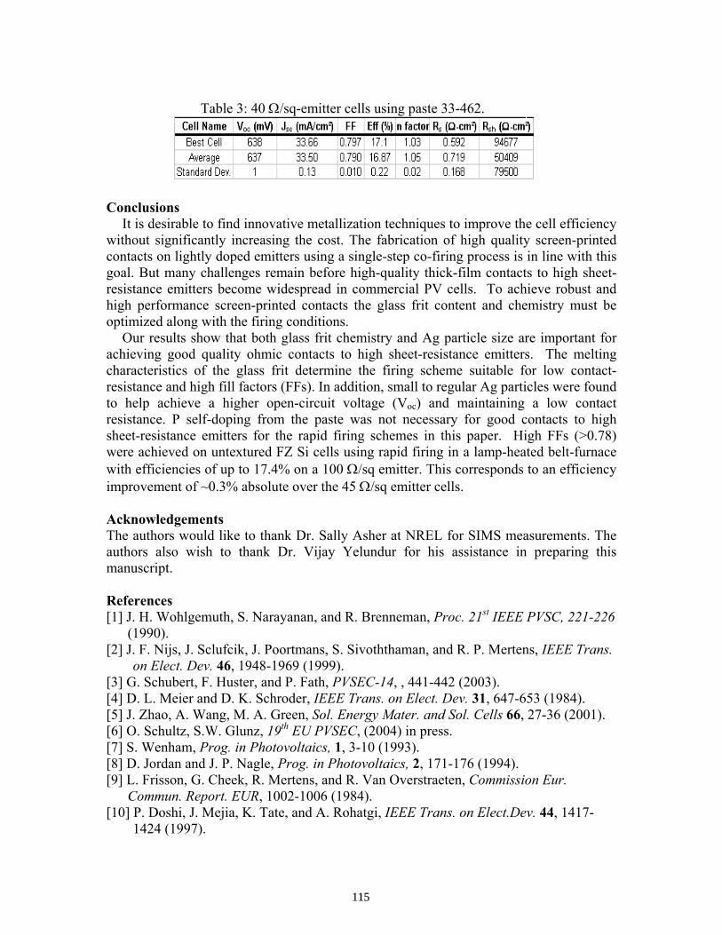
Conclusions
It is desirable to find innovative metallization techniques to improve the cell efficiency without significantly increasing the cost. The fabrication of high quality screen-printed contacts on lightly doped emitters using a single-step co-firing process is in line with this goal. But many challenges remain before high-quality thick-film contacts to high sheet-resistance emitters become widespread in commercial PV cells. To achieve robust and high performance screen-printed contacts the glass frit content and chemistry must be optimized along with the firing conditions.
Our results show that both glass frit chemistry and Ag particle size are important for achieving good quality ohmic contacts to high sheet-resistance emitters. The melting characteristics of the glass frit determine the firing scheme suitable for low contact-resistance and high fill factors (FFs). In addition, small to regular Ag particles were found to help achieve a higher open-circuit voltage (Voc) and maintaining a low contact resistance. P self-doping from the paste was not necessary for good contacts to high sheet-resistance emitters for the rapid firing schemes in this paper. High FFs (>0.78) were achieved on untextured FZ Si cells using rapid firing in a lamp-heated belt-furnace with efficiencies of up to 17.4% on a 100 Ω/sq emitter. This corresponds to an efficiency improvement of ~0.3% absolute over the 45 Ω/sq emitter cells. Acknowledgements The authors would like to thank Dr. Sally Asher at NREL for SIMS measurements. The authors also wish to thank Dr. Vijay Yelundur for his assistance in preparing this manuscript. References [1] J. H. Wohlgemuth, S. Narayanan, and R. Brenneman, Proc. 21st IEEE PVSC, 221-226 (1990). [2] J. F. Nijs, J. Sclufcik, J. Poortmans, S. Sivoththaman, and R. P. Mertens, IEEE Trans.
on Elect. Dev. 46, 1948-1969 (1999). [3] G. Schubert, F. Huster, and P. Fath, PVSEC-14, , 441-442 (2003). [4] D. L. Meier and D. K. Schroder, IEEE Trans. on Elect. Dev. 31, 647-653 (1984). [5] J. Zhao, A. Wang, M. A. Green, Sol. Energy Mater. and Sol. Cells 66, 27-36 (2001). [6] O. Schultz, S.W. Glunz, 19th EU PVSEC, (2004) in press. [7] S. Wenham, Prog. in Photovoltaics, 1, 3-10 (1993). [8] D. Jordan and J. P. Nagle, Prog. in Photovoltaics, 2, 171-176 (1994). [9] L. Frisson, G. Cheek, R. Mertens, and R. Van Overstraeten, Commission Eur. Commun. Report. EUR, 1002-1006 (1984). [10] P. Doshi, J. Mejia, K. Tate, and A. Rohatgi, IEEE Trans. on Elect.Dev. 44, 1417-
1424 (1997).
Table 3: 40 Ω/sq-emitter cells using paste 33-462.
115

[11] T. Bruton, N. Mason, S. Roberts, O. N. Hartley, S. Gledhill, J. Fernandez, R. Russel, W. Warta, S. Glunz, O. Schultz, M. Hermle, and G. Wileke, WCPEC-3 (2003).
[12] D. S. Ruby, P. Yang, M. Roy, and S. Narayanan, Proc. 26th IEEE PVSC, 39-42 (1997).
[13] J. Horzel, J. Szlufcik, J. Nijs, and R. Mertens, Proc. 26th IEEE PVSC, 139-142 (1997).
[14] A. Rohatgi, M. Hilali, D. L. Meier, A. Ebong, C. Honsberg, A. F. Carroll, and P. Hacke, Proc. 17thEU PVSEC, 1307-1310 (2001).
[15] L. M. Porter, A. Teicher, and D. L. Meier, Sol. Energy Mater. and Sol. Cells 73, 209-219 (2002).
[16] F. Rollert, N. A. Stolwijk, and H. Mehrer, J. Phys. D 20, 1148-1155 (1987). [17] S. A. Campbell, The Science and Engineering of Microelectronic Fabrication,
Oxford University Press: New York (1996). [18] C. Ballif, D. M. Huljić, A. Hessler-Wysser, and G. Willeke, Proc. 29th IEEE PVSC,
360-363 (2002). [19] C. Ballif, D. M. Huljić, G. Willeke, and A. Hessler-Wysser, Appl. Phys. Lett. 82,
1878-1880, (2003). [20] G. Schubert, F. Huster, and P. Fath, 19th EU PVSEC, (2004) in press. [21] G. Schubert, B. Fischer, and P. Fath, Photovolt. in Europe Conf., Rome, (2002). [22] G. Schubert, F. Huster, ad P. Fath, PVSEC-14, (2004) pp. 441-442. [23] R. J. S. Young and Alan F. Carroll, Proc.16th EU PVSEC, 1731-1734 (2000). [24] A. Shaikh, S. Sridharan, T. Pham, and C. Khadilkar, 3rd WCPEC, (2003). [25] R. Mertens, M. Eyckmans, G. Cheek, M. Honore, and R. Van Overstraten, Proc. 17th IEEE PVSC, 1347-1351 (1984). [26] G. C. Cheek, R. P. Mertens, R. Van Overstraeten, and L. Frisson, IEEE Trans. on
Elect. Dev. 31, 602-609 (1984). [27] K. Firor, S. J. Hogan, J. M. Barrett, and R. T. Coyle, Proc.16th IEEE PVSC, 824-
827(1982). [28] O Growski, L. Murawski, and K. Trzebiatowsky, J. Phys. D: Appl. Phys. 15, 1097-
1101 (1982). [29] T. Nakajima, A. Kawakami, and A. Tada, Internat. J. of Hybrid Microelect. 6, 580-
586 (1983). [30] M. M. Hilali, A. Rohatgi, and S. Asher, IEEE Trans. on Elect. Dev., 51, 948-955
(2004). [31] M. Bähr, S. Dauwe, L. Mittelstädt, J. Schmidt and G. Gobsch, 19th EU PVSEC,
(2004) in press. [32] H. H. C. de Moor, A. W. Weeber, J. Hoornstra, and W. C. Sinke, 6th Workshop on
Cryst. Si Sol. Cell Mater. and Processes, 154-170 (1996). [33] S. M. Sze, Physics of Semiconductor Devices, 2nd ed. John Wiley & Sons: New York
(1981). [34] M. Van Craen, L. Frisson, and F. C. Adams, Surface and Interface Analysis 6, 257-
260 (1984). [35] R. A. Sinton and A. Cuevas, Proc. of the 16th EU PVSEC II, 1152-1155 (2000).
116
Low frequency direct-PECVD SiNx films for rear surface passivation Stefaan De Wolf, Guido Agostinelli and Guy Beaucarne IMEC vzw, Kapeldreef 75, B-3001 Leuven, Belgium Petko Vitanov Bulgarian Academy of Sciences, 72 Tzarigradsko Chaussee Blvd., 1784 Sofia, Bulgaria In this paper we report on the use of direct-plasma enhanced chemical vapor deposited (PECVD) silicon nitride (SiNx) films deposited at low excitation frequency (440kHz) on low resistivity (1.5Ω.cm) p-type Cz silicon substrate surfaces with different texture, to elucidate the influence of micro-roughness of the substrate surface on the surface-passivating properties of thin SiNx films. The less pronounced the surface texture is, the better Si-rich SiNx films are capable of providing good surface passivation. Noticeably, when short high temperature (firing) treatments are applied upon passivation layer deposition, the process-window to yield good surface passivation broadens, although very Si-rich films tend to suffer from blistering. I. INTRODUCTION
Thin amorphous SiNx dielectric layers have found many applications in a great
variety of electronic devices in the past years, including the use as anti reflective coating (ARC), as surface- and as bulk-passivation layer in crystalline silicon solar cells. For surface passivation, most of the work has been focused in the past on the n+ front-side emitter passivation of high efficiency solar cells1. However, the trend towards the use of thinner substrates (<150µm), brought up the need for excellent surface passivation of the p-type rear-side base of solar cells. Due to the large capture cross section ratio (σn/σp≈100 at midgap) of minority to majority carriers, the passivation of surfaces in p-type silicon is more critical than in n-type silicon2. Most of the surface-passivation studies have been focused in the past on polished surfaces. However, in a process-related environment, this type of surface is rarely achieved, on the contrary, most surfaces are often rather rough mainly due to the inherent presence of wire-saw damage at the surfaces that still needs to be removed and often due to front surface texturing reasons. Hence, in this paper we report on the use of SiNx layers for the surface passivation of non polished p-type Si substrates. For a practical applicable rear surface passivation layer, it is important that it can give rise to low surface recombination velocities, especially at rather low values for the injection level ∆n, corresponding with a solar cell operating under an AM1.5 100mW.cm-2 spectrum, even on non polished samples. A second practical requirement is that the layer should remain as thermal hard as possible to avoid degradation upon further processing. II. SURFACE PASSIVATION
Charges present at the SiNx – Si interface will induce a band bending surface
potential ψs in the semiconductor, yielding a change in density of charge carriers at the surface. The knowledge of these densities, combined with knowledge over the interface
117

states, allows the calculation of the surface recombination velocity Sit, which is derived from standard Shockley-Read-Hall theory3 (see also figure 1):
[ ]
⌡
⌠
−
−++
−
+
−∆
=
v
c
E
E
it
itpiit
isitniit
is
issitititnitpthit dE
EkT
EEnpEkT
EEnn
nnpEDEEn
vS)(exp)(exp
)()()( 2
σσ
σσ (1)
( )
∆+=
kTqnnn s
psψexp0
and ( )
−∆+=
kTqnpp s
psψexp0
(2)
ns and ps are the electron and hole concentrations at the surface, np0 and pp0 are the equilibrium carrier concentrations in the bulk , ∆n is the excess carrier concentration being injected, ψs the surface potential, vth the thermal velocity, and Ei the intrinsic Fermi level. The density of interface states at a given energy level Eit is given by Dit(Eit).
0.15 0.1 0.05 0 0.05 0.1 0.15 0.2 0.251
10
100
1 .103
1 .104
1 .105
105
1
S ψ s 1015, 1014, 5 1010⋅,
S ψ s 1016, 1014, 5 1010⋅,
S ψ s 1017, 1014, 5 1010⋅,
S ψ s 1016, 1010, 5 1010⋅,
S ψ s 1016, 1012, 5 1010⋅,
S ψ s 1016, 1016, 5 1010⋅,
0.30.2− ψ s Fig. 1. Relation between surface recombination velocity and the induced surface potential ψs for 1Ohm.cm p-type material in case a single interface defect is assumed, positioned at midgap. Solid line: Na=1016cm-3 and ∆n=1014cm-3. Dit(Eit) = 1.0x1012cm-2eV-1 Eit=Ei, σn(Eit)= 1.0x10⁻¹³cm-2 , σp(Eit)= 1.0x10⁻¹⁵cm-2.
The charge densities playing a role in the determination of ψs are respectively
associated with the fixed charges Qf stored in the SiNx layer, charges Qit stored by interface traps, and charges Qg present at the gate electrode (in case the SiNx layer is covered by a metal). If QSi is the charge density in the silicon, the sum of all charges must balance:
0=+++ Siitgf QQQQ (3) From this, Girisch et al. derived an algorithm to determine ψs
4, which was later used by Aberle et al. for Si-SiO2 interface studies5. In the absence of an electrode or chargeable interface states, and for a given density of (positive) fixed charges in the SiNx layer, higher doping levels yield lower surface potentials. Conversely, lower injection-levels give higher effective values for ψs (see figure 2). The presence of chargeable interface states results in a smaller required density Qf to obtain an equally large value for ψs, especially when the interfacial state density is of the same order or larger than the fixed charge density. When the value of ψs drives the semiconductor into inversion, it is important to
Na ∆n
Sit [cm.s-1]
1016
1017
1015
1016
1014
1012
1010
118

note there exist a subsurface region (down to 100nm deep) where the density of minority and majority charge carriers are equal, hence a subsurface region with very effective SRH dynamics can exist, especially when surface states extend into the bulk of the material. For low injection levels, the depletion region recombination can even dominate over the actual surface recombination6.
0.2 0 0.2 0.4 0.61 .1010
1 .1011
1 .1012
1 .1013
1013
1010
Q sc ψ 1016, 108,( )
Q sc ψ 1016, 1010,( )
Q sc ψ 1016, 1012,( )
Q sc ψ 1016, 1014,( )
Q sc ψ 1016, 1016,( )
Q sc ψ 1015, 1014,( )
Q sc ψ 1017, 1014,( )
Q sc ψ 1018, 1014,( )
Q sc ψ 1019, 1014,( )
0.80.3− ψ Fig. 2. Relation between charges present in SiNx layers and the induced surface potential ψs. Assumptions: no chargeable interface states and no gate electrode. Solid line: Na=1016cm-3 and ∆n=1014cm-3. The dotted and dashed arrows respectively show the evolution towards increasing value for ∆n and Na.
From expression (1), it can thus be understood that the passivation of a silicon
surface fundamentally can be done in two different ways5: by electrical field effect passivation or by neutralization of interface defect states. In the first case, the presence of e.g. charges in a dielectric film covering the substrate can result in the presence of a band bending potential ψs at the surface. This can then reduce the surface concentration of one type of carriers and therefore determine a decrease in the surface recombination rate. In the second case the value for Dit(Eit) is reduced by chemical passivation of the interface defect states. Typically this can done by hydrogen atoms, which are saturating the dangling Si bonds present at the surface. III. FILM PROPERTIES A. Hydrogen
In the past, Lauinger et al. found a clear increase in τeff of samples with increasing value for the diffractive index n of SiNx layers for shiny etched p-type 1-2Ωcm float-zone (FZ) silicon wafers. Saturation occurred for values of n above 2.47. Generally speaking, an increase in the value for n corresponds with the deposition of more Si-rich nitride layers. Other authors reported that with decreasing value for the gas flow ratio R=[NH3]/[SiH4]
∆n
Na
1013
1012
1011
1010
Qf
1016
1014
1012
1010
108
1016
1015
1017
1018
1019
119

(and thus layer content x), the Si-H content in these layers increases, while the N-H content decreases. This was seen both for direct PECVD SiNx (precursor gasses: SiH4/N2/H2)8 as for remote PECVD SiNx (precursor gasses: SiH4/NH3)7,9. The minimum hydrogen content in the films was found at x~1.110. The best surface passivation was again achieved for the lowest values of R, which corresponds to these SiNx alloys that have the highest density of Si-H bonds8. B. Charges present in SiNx layers
On the other hand, SiNx layers can contain quite a number of charges, depending on the deposition method and the ratio of process gasses used. In amorphous SiNx ,,, the Si dangling bond is considered to be the dominant deep defect11. This dangling bond exists in a configuration where the Si atom is back bonded by either Si or N atoms: Si≡Si3-yNy (where y equals 1, 2, or 3)12. In Si-rich samples most of the dangling bonds are in a configuration where y=0, and for higher values of x the number of back-bonded Si atoms decreases in favour of N atoms13. For the case where y=3, the defect is known as the K center, which is believed to be amphoteric, and in as-deposited material it is either positively (K+) or negatively (K-) charged. UV illumination causes electron-hole pairs to become trapped/emitted at these preexisting positive or negatively charged sites, which then become electrically neutral. Conversely, by hole-injection at a paramagnetic UV generated K center, a positively charged diamagnetic site is generated, while for electron-injection, the K center becomes negatively charged and diamagnetic14. Aberle argued that prior UV illumination, away from the Si-SiNx interface, a ~20nm deep section of the nitride film exists hosting positively charged (K+) centers, strongly dependent on the electron and hole concentration at the Si surface15. Apart from the K center related variable charge, it is also believed a fixed positive charge is present in the interfacial SiNxOy film, sandwiched between the substrate and the actual SiNx layer15,16. Mäckel reported an increase in number of (K+) center related defects with increasing x from 0 to 1, for direct PECVD SiNx (process gasses: SiH4/N2/H2)8. Schuurmans on the other hand reported a decrease in number of positive fixed charge with increasing values for x from about 0.8 to 1.617 [17], which agrees with e.g.18,19.
From dark Capacitance Voltage (CV) curves (f=1Mhz) measured for low frequency fired direct plasma SiNx films on polished Si wafers, it is seen that depending on the voltage sweep, a different amount of charges can be present. For samples with R=5.85, measurements starting at -40V (+40V), show a very large hysteresis effect, suggesting a large density of positively (negatively) charged traps is present in the SiNx layer. This layer corresponds with a layer as is used for ARC purposes. The calculated values of the charge density under these two extreme conditions is given in table 2, for the different studied SiNx layers. The total charge density in the SiNx layers can be written as the sum of fixed charges and chargeable traps:
),()(),( * starttfstartf VRQRQVRQ ±=± (4)
120
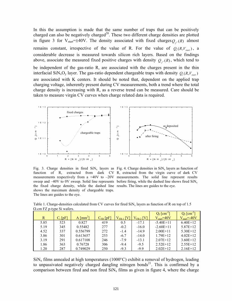
In this the assumption is made that the same number of traps that can be positively charged can also be negatively charged20. These two different charge densities are plotted in figure 3 for Vstart=±40V. The density associated with fixed charges )(* RQ f
almost
remains constant, irrespective of the value of R. For the value of ),( startt VRQ , a considerable decrease is measured towards silicon rich layers. Based on the findings above, associate the measured fixed positive charges with density )(* RQ f
, which tend to
be independent of the gas-ratio R, are associated with the charges present in the thin interfacial SiNxOy layer. The gas-ratio dependent chargeable traps with density ),( startt VRQ are associated with K centers. It should be noted that, dependent on the applied trap charging voltage, inherently present during CV measurements, both a trend where the total charge density is increasing with R, as a reverse trend can be measured. Care should be taken to measure virgin CV curves when charge related data is required.
Fig. 3. Charge densities in fired SiNx layers as function of R, extracted from dark CV measurements respectively from a +40V to –20V sweep and –40V to 0V sweep. Solid line represents the fixed charge density, while the dashed line shows the maximum density of chargeable traps. The lines are guides to the eye.
Fig. 4. Charge densities in SiNx layers as function of R, extracted from the virgin curve of dark CV measurements. The solid line represent results before firing, while the dashed line shows fired SiNx results. The lines are guides to the eye.
Table 1. Charge-densities calculated from CV curves for fired SiNx layers as function of R on top of 1.5 Ω.cm FZ p-type Si wafers.
R Ci [pF] A [mm2] CFB [pF] VFB-1 [V] VFB-2 [V]Qf [cm-2]
Vstart=40V Qf [cm-2]
Vstart=-40V 5.85 523 0.827 419 0.5 -17.1 -5.40E+11 6.40E+12 5.19 345 0.55482 277 -0.2 -16.0 -2.60E+11 5.87E+12 4.52 337 0.556799 272 -1.4 -14.9 2.00E+11 5.30E+12 3.86 301 0.613657 253 -6.7 -14.0 1.79E+12 4.02E+12 3.19 291 0.617108 246 -7.9 -13.1 2.07E+12 3.60E+12 1.86 363 0.76728 306 -9.4 -9.5 2.52E+12 2.55E+12 1.20 287 0.749029 250 -9.3 -9.9 2.02E+12 2.16E+12
SiNx films annealed at high temperatures (1000°C) exhibit a removal of hydrogen, leading to unpassivated negatively charged dangling nitrogen bonds21. This is confirmed by a comparison between fired and non fired SiNx films as given in figure 4, where the charge
0 1 2 3 4 5 61 E 1 0
1 E 1 1
1 E 1 2
1 E 1 3
Qf[
cm
-2
]
R = [ N H3
] / [ S i H4
]0 1 2 3 4 5 6
1 E 1 2
1 E 1 3
Qf[
cm
-2
]
R = [ N H 3 ] / [ S i H 4 ]
fixed charges
chargeable traps
as deposited
after firing
121

density is calculated based on virgin CV curves, to avoid excessive charging of traps due to the applied measurement biases. IV. SURFACE PREPARATION
In a low-cost environment, saw damage removal and surface texturing can be done either with alkaline etching, acidic isotropic texturing (which can be followed by a lowly concentrated alkaline etching dip to remove the present porous silicon on the surface), or selective plasma texturing22. The back-region emitter, which is present upon POCl3 emitter diffusion, can be removed in similar ways, including wet acidic CP4 (HF:HNO3:CH3COOH) polishing solutions. With the latter technique, prolonged etching yields smoother surfaces.
In our experiments (upon texturing, POCl3 diffusion and (bifacial) emitter removal) the wafers were thoroughly cleaned ((H2SO4:H2O2)(4:1) – rinsing in de-ionised water – HF(2%)-dip – rinsing in de-ionised water). Subsequently, the samples were passivated by three different passivation layers: either by standard PECVD SiNx:H (as for ARC, f= 440kHz), by the for FZ Si material optimised PECVD Si-rich SiNx:H (f=440kHz), or by PECVD a-Si:H as optimised for surface passivation (f=13.56Mhz). All employed samples were neighbouring p-type 1Ω.cm multi crystalline or Cz wafers. Effective minority charge carrier lifetimes were then extracted from the samples by the Quasi Steady State Photoconductance technique23.
Interestingly, in figure 5 it can be seen that none of the samples of which the preparation prior to cleaning was terminated with an alkaline etching step, could be well-passivated afterwards, irrespective of the employed passivation layer. Even for the group of samples of which the bifacial emitter was etched off in an isotropic acidic texturing solution (which was followed by a very low concentration (cold) alkaline etching dip to remove the present porous silicon) this holds. It should be stressed that prior to surface passivation, the wafers were thoroughly cleaned. A possible explanation why alkaline treated samples do not allow any surface passivation might be that upon passivation layer deposition, leftover traces of alkali ions form mobile charges cancelling out any possibility to obtain good surface passivation, as has been experienced in the past for thermally grown silicon dioxide passivation layers15. Note that alkaline treatments prior to emitter diffusion can still allow good surface passivation, as long as there is no alkaline related step involved for removal of the emitter. FIG. 5. Influence of the surface preparation on the surface passivating properties of direct PECVD SiNx:H and a-Si:H layers on 1 Ω.cm PV Silicon mc-Si material (∆n = 1016cm-3). E.R. = Emitter Removal.
τeff [µs]
0
20
40
60
80
100
120
140
textture: acidicE.R.: acidic
texture: acidicE.R.: CP4
texture: alkalineE.R.: alkaline
texture: alkalineE.R.: CP4
a-Si (HF)
Si-rich SiNx (LF)
ARC SiNx (LF) fired
122

V. SURFACE TEXTURE From figure 5, it is clear that the preferential etching method does not include an
alkaline treatment. As discussed before, prolonged etching in wet acidic polishing solutions yields smoother surfaces. To check the influence of the surface roughness, different low frequency direct SiNx:H layers were deposited on samples with increasing mean roughness.
FIG 6. Effective lifetime τeff before firing as measured by QSSPC at an excess charge carrier concentration of ∆n = 1.1014cm-3. The lines are guides to the eye. Samples A, B and C respectively correspond with an RMS roughness of about 115nm, 70nm and 10nm.
FIG 7. Effective lifetime τeff after firing as measured by QSSPC at an excess charge carrier concentration of ∆n = 1.1014cm-3. The lines are guides to the eye. Samples A, B and C respectively correspond with an RMS roughness of about 115nm, 70nm and 10nm.
A. Passivation results after deposition
In figure 6, τeff versus R is presented for samples with different degrees of texture, achieved by chemical polishing. A certain degree of scattering in the data is due to the employed material (Cz-Si) in the experiments. It can be seen that depending on the surface texture, a different passivation behavior is observed throughout a change in the value for R: • For the more polished samples, the best surface passivation is obtained for the most
Si-rich SiNx films. • The more texture the samples exhibit, the more it seems that very Si-rich SiNx layers
do not yield good surface passivation any longer. A (local) maximum in τeff can be found at values for R shifting from 1 (most polished sample) to 2.5 (most rough sample).
B. Passivation results after short thermal annealing
Figure 7 shows again τeff of the samples, but now after a short high temperature step in a conveyor belt type of furnace, comparable to the contact firing-process at the end of a solar cell process. In this graph, it can be seen that:
123

• Independent of the type of substrate roughness, very Si-rich SiNx layers (R<1) no longer give rise to any surface passivation. Moreover, this type of layer looks completely destroyed after a firing treatment. This is believed to be caused by so-called blistering of the SiNx layers: the release of excessive amounts of hydrogen from the layer upon thermal excitation.
• For the other types of SiNx layers (R>1), it seems to be that the lifetime data largely levels out: the surface roughness and exact gas composition play a less important role.
VI. CONCLUSIONS In this paper, we discussed the use of low frequency direct Plasma Enhanced Chemical Vapor Deposited SiNx films to achieve good surface passivation on p-type Si (rough) substrates. It was found that a very high amount of K-centers is present in layers as optimized for ARC purposes (R~5.85). The more Si-rich the layer, the less K-centers are present. Secondly, surface preparation techniques should avoid the use of alkaline solutions, since they tend to be lifetime-killers. Finally, very good surface passivation can be achieved on polished samples when using Si-rich nitrides. The introduction of surface texture increases the surface recombination velocity. However, thermal firing treatments tend to broaden the useful processing-window. 1 M.J. Kerr, J. Schmidt, and A. Cuevas, J. Appl. Phys. 89, 3821 (2001). 2 Y. Bai, J.E. Phillips, and A.M. Barnett, IEEE Trans. Electron Dev. 45 1784 (1998). 3 W.D. Eades and R.M. Swanson, J. Appl. Phys. 58 4267 (1985). 4 R.B.M. Girisch, R.P. Mertens, and R.F. de Keersmaecker, IEEE Trans. Electron Dev. 35, 203 (1988). 5 A.G. Aberle, S. Glunz, and W. Warta, J. Appl. Phys. 71 4422 (1992). 6 S. Dauwe, Ph.D. Thesis, Universität Hannover (2004) 7 T. Lauinger, J. Moschner, A.G. Aberle, and R. Hezel, J. Vac. Sci. Technol. A 16 (2), 530 (1998). 8 H. Mäckel and R. Lüdemann, J. Appl. Phys. 92 (5), 2602 (2002). 9 A. Weeber, H.C. Rieffe, W.C. Sinke, and W.J. Soppe, to be published in Conf. Record 19th European
Photovoltaic Solar Energy Conference and Exhibition, Paris, France 10 S. Garcia, D. Bravo, M. Fernandez, I. Martil, and F.J. López, Appl. Phys. Lett. 67 (22), 3263 (1995). 11 S. Fujita and A. Sasaki, J. Electrochem. Soc. 132, 398 (1985). 12 D. Jousse, J. Kanicki, and J.H. Stathis, Appl. Phys. Lett. 54, 1043 (1989). 13 S. Hasegawa, M. Matsuda, and Y. Kurata, Appl. Phys Lett. 58 (7), 741 (1991). 14 W.L. Warren, J. Kanicki, F.C. Rong, and E.H. Pointdexter, J. Electrochem. Soc. 139, 880 (1992), and
references therein. 15 A.G. Aberle, Crystalline silicon solar cells: advanced surface passivation and analyses, University of
New South Wales, Centre for photovoltaic engineering Sydney (1999). 16 J. Schmidt and A.G. Aberle, J. Appl. Phys. 85, 3626 (1999). 17 F. Schuurmans, Ph.D. Thesis, Universiteit Utrecht (1998). 18 D. Landheer, G.C. Aers, G.I. Sproule, R. Khatri, P.J. Simpson, and S.C. Gujrathi, J. Appl. Phys. 78, 2568
(1995). 19 R. Hezel and R. Schörner, J. Appl. Phys. 54, 3076 (1981). 20 W.S. Lau, S.J. Fonash, and J. Kanicki, J. Appl. Phys. 66 2765 (1989). 21 F.H.P.M. Habraken, M. Heyns, H.E. Maes, R. de Keersmaecker, A.E.T. Kuyper, and W.F. van der Weg,
in Low Pressure Chemical Vapor Deposited Silicon Oxynitride Films, Materials and Applications, Edited by F.H.P.M. Habraken, Research Reports ESPRIT (Springer, Heidelberg, 1991).
22 H.F.W. Dekkers, G. Agostinelli, D. Dehertoghe, and G. Beaucarne, to be published in Conf. Record 19th European Photovoltaic Solar Energy Conference and Exhibition, Paris, France.
23 R.A. Sinton and A. Cuevas, Appl. Phys. Lett. 69, 2510 (1996).
124

Vision of GE Charlie Korman
Manuscript not available at time of printing.
125

SPHERAL SOLAR™ CELL PROCESS AND DESIGN AT FACTORY START-UP
Gary Stevens; [email protected] Milfred Hammerbacher; [email protected]
Paul Sharrock; [email protected] Brad Kachuik; [email protected] Aline Wullur; [email protected] Khalil Zeaiter; [email protected]
Spheral Solar Power, a division of ATS Automation Tooling Systems
25 Reuter Dr., Cambridge, ON Canada N3E 1A9 Tel: (519)650-6505; Fax: (519)650-6519;
ABSTRACT: Factory production of the new design is commencing. The antireflection coating of the spheres prior to metallurgical bonding of the front contact foil enables an innovative optical mini concentrator design. Spherical cups are formed into the perforated foil prior to bonding, allowing the sphere population in the cell to be reduced by 50%. The bond process dissolves the TiO2 coating at the bond line. Post-deposition treatments of the antireflection coating have been instituted for improved density and uniformity, providing the needed process control improvement for the bonding process.
1 INTRODUCTION
The use of silicon granules or spheres in a conductive matrix for photovoltaics dates back almost fifty years [1, 2] when silicon wafers were only 25mm in diameter. In subsequent years ideas went from beads in a polymer matrix to a glass matrix with rear metal contacts and transparent oxide front contacts [3]. Even at that stage of evolution, the primary researchers recognized the need to use the surfaces between the beads as reflective collectors [4, 5].
In the early eighties, a breakthrough was made through metallurgical bonding of aluminum foil to spheres [6] allowing for a return to a flexible structure. Significant cost benefits were realized with this design change but there was still an opportunity for significant reductions in silicon utilization.
During the design phase of the SSP factory, a major effort was undertaken to develop an optimum optical structure in the front contact foil. A move from 100 X 300 mm cells to 150 X 600 mm cells occurred during this effort, providing a challenge for pressing an optical structure into the foil. 2 TITANUIM OXIDE DEPOSITION
The original Spheral Solar™ cells received the antireflection coating after bonding to the front contact foil, either in a batch chamber [7] or a conveyor system. With this approach, it was not possible to prevent TiO2 deposition on the foil, so the spheres were placed as close together as possible.
To have optimum reflectivity in a spherical cup, mini-concentrator foil, the coating must be applied to the spheres prior to foil bonding. During the thermo-compression bond of the spheres to the perforated foil, the contact area of aluminum very nearly becomes liquid, allowing the TiO2 to be dissolved at the bond line.
A large batch fluid bed reactor has been designed for the deposition process, based on the standard APCVD deposition through decomposition of tetra-iso-propyl titanate (TPT). The process works quite well, with good uniformity and coating efficiency. Coated spheres subsequently bonded to optically formed perforated foils
require a hydrofluoric acid backside TiO2 removal prior to backside etch (BSE), which exposes the p-type core for back-lit probe (BLP). SEM photographs of one of the spheres is shown in Figure 1. BLP data and sphere punch-out forces demonstrate that metallurgical bonding occur through the TiO2 to the silicon. Removal of the aluminum foil with dilute Hydrochloric acid shows clean removal of a ring of the TiO2 at the bond line.
Figure 1: SEM photographs of the TiO2 coating
126

3 TiO2 DENSIFICATION The original Spheral Solar™ process relied on a deep emitter to prevent spiking of aluminum through the junction during metallurgical bonding. A subsequent silicon etch (usually 100:1 HNO3 : HF) was used to thin the emitter for improved collection efficiency, leaving a deep emitter under the metal contacts. With the change in process sequence, it is necessary to start with a shallow emitter and eliminate the front side thin (FST) process. As the fluid bed TiO2 deposition is run at a relatively low temperature (<400°C), there is a need to reduce film porosity to provide improved uniformity of the aluminum bond. A high temperature sintering process has been shown by other authors to accomplish this [8]. The same authors have also shown that it is possible to grow a SiO2 layer underneath the TiO2 coating, which can provide good surface passivation [9]. By sintering the spheres at temperatures of at least 750°C for short periods, the deposited film shows significant growth in the size of the grains. Figure 2 shows SEM photographs before and after sintering at these temperatures.
Before
After Figure 2: SEM photographs of TiO2 before and after
sintering at 750°C. This step has been quite important in preventing aluminum spiking through the junction, which would short circuit the sphere. Fortunately, spheres that have been shorted are eliminated from the circuit by an anodization process called Selective Electro-dissolution (SED) before bonding of the back contact. Optimization of the sintering process has been completed. Variations of temperature, time and gases have been shown to considerably modify the interaction between the perforated foil and TiO2 during bonding.
Table 1 shows a summary from automatic BLP probing of spheres bonded to a flat perforated foil. Whether the atmosphere is pure nitrogen, or a nitrogen/oxygen mixture, VOC is increased by at least 5% compared to spheres without densification. However, as indicated by the data in Table 1, a significant effect on shunted and leaky diodes is obtained. This is perhaps due to a difference in the thickness or structure of an SiO2 layer formed at the TiO2/Si interface.
Table I: Summary of Auto BLP Results
N2 a
nd O
2 Rat
io
N2 F
low
rat
e (lp
m)
O2 F
low
rat
e (lp
m)
Avg
Voc
(mV
)
Avg
Isc
(µA
)
% B
ad
% Y
ield
%
Shu
nt
% O
pen
% B
ad C
onta
ct
% L
eaky
%
Dou
ble
Dio
des
Tot
al L
eaky
and
Shu
nts
Baseline (100% N2)
3 0 559 111 0 88 6 0 0 6 0 12
½ N2 and ½ O2
3 3 564 112 1 93 4 0 0 3 0 7
Further studies are planned to attempt to obtain images and compositional data at this interface. Bond condition variations must be minimized to eliminate poor diode characteristics that result from aluminum spikes. 4 OPTICAL STRUCTURE The design of the current mini-concentrator optics was innovated before start-up of the pilot line at ATS Automation. Many considerations had to be included in the design such as constraints for building a tool to press the structure into the foil. Flow of the metal during pressing would be a very important factor, both to ensure all features of the optical structure are filled as well as to minimize the force required to accomplish this. A final consideration in the optics design is the thermo-compression bonding process. Since this is accomplished by using aluminum pressure pads with a release coating, to minimize damage to the spheres, the height of the optical structure had to be limited to about the midpoint of the spheres. The illustration in Figure 3 shows one of the designs which was developed from optical modeling. This is a hexagonal array with shallow spherical cups having a radius approximately twice that of the spheres. With aluminum reflectivities in the 80 – 90 % range, the model indicated collection efficiencies would be equivalent to that of a close packed array on a flat foil.
Figure 3: Illustration of Optical Structure Cells with this structure are now routinely built in the factory on 150 X 600mm foils. Many size ranges of spheres are used with the same foil geometry without significant variations in efficiency, proving the optics are
127

well focused to the center of the spheres. The location of the spheres is quite critical, requiring precise location of perforation in the cup bottom. The tops of the structure (triple points) are at the correct height to avoid crushing by the bonding pads. Figure 4 shows two LBIC images of active cells built using the new optical structure. The sharp knife edges and the triple points where the cups meet are somewhat essential for optimum collection efficiency. If the structure is poorly formed (top image) incident light will be scattered away from the spheres. A well formed foil effectively reflects most incident light into the spheres (bottom image).
Poorly formed foil
Well Formed Foil Figure 4: LBIC images of poorly formed and well formed
foils.
5 CONCLUSION A robust titanium dioxide antireflection coating is uniformly applied to spheres in a batch fluid bed reactor. During thermo-compression bonding of coated sphere to perforated aluminum foil, the aluminum dissolves the titanium dioxide, allowing for ohmic contact to the n-type silicon surface. Modifications of the titanium dioxide coating by a post-deposition sintering process provides the necessary reaction control to prevent aluminum from reaching the p-type silicon core during bonding. A shallow spherical cup pressed into the perforated aluminum foil allows for silicon usage to be cut in half by increasing the sphere center-to-center spacing. Equivalent cell performance has been demonstrated with this reduced sphere count design, compared to the original close-packed design. Full foil forming of the optical structure and precise centering of the spheres is critical for optimum cell performance. Further studies with titanium dioxide densification, post-bond sintering, and foil surface modifications are expected to improve cell efficiency well beyond the >10% efficiency that has already been achieved. 6 REFERENCES
1. M. Paradise, US Patent 2,904,613 - Filed August 26, 1957, Issued September 15, 1959
2. E. Ralph, US Patent 3,025,335 - Filed February 29, 1960, Issued March 13, 1962
3. J. Kilby, et.al., US Patent 4,021,323 – Filed July 28, 1975, Issued May 3, 1977
4. A. Appleby, US Patent 4,454,372 – Filed April 17,1981, Issued June 12, 1984
5. K Carson, et.al., US Patent 4,614,835 – Filed December 15,1983, Issued September 30, 1986
6. M. Jensen and J.D. Levine, US Patent 4,872,607 – Filed September 26, 1988, Issued October 10, 1989
7. S. Parker, et.al., US Patent 5,081,069 – Filed December 26, 1989, Issued January 14, 1992
8. B. Richards, et.al., World Conference on Photovoltaic Energy Conversion, Osaka, May 12 – 16, 2003
9. B. Richards, et.al., 28th IEEE Photovoltaic Specialists Conference, Anchorage, September 15 – 22, 2000
128

DETECTION OF HYDROGEN IN MULTICRYSTALLINE SILICON
G. Hahn1, D. Sontag1, S. Seren1, A. Schönecker2, A.R. Burgers2, R. Ginige3, K. Cherkaoui3, D. Karg4, H. Charifi4
1University of Konstanz, Department of Physics, PO Box X916, 78457 Konstanz, Germany 2ECN Solar Energy, PO Box 1, 1755ZG Petten, Netherlands
3NMRC, Lee Maltings, Prospect Row, Cork, Ireland 4Institute of Applied Physics, University of Erlangen, Staudtstr. 7, 91058 Erlangen, Germany
Tel: +49-7531-88-3644, Fax: +49-7531-88-3895. Email: [email protected] ABSTRACT: Hydrogenation kinetics of defected mc Si materials has been investigated. Deuterium originating from a hydrogen-rich PECVD SiN layer could be detected deep in the bulk of oxygen-rich RGS material by SIMS after a firing step. A model for hydrogen diffusion is described, which is based on the monitoring of the overall O and C concentration, [Oi], [Cs], and vacancy concentrations in the as-grown wafers as well as after emitter diffusion. Trapping of hydrogen at oxygen precipitates can explain the observed D-profiles. Precipitation of oxygen is a function of as-grown [Oi] and thermal pre-treatment. If [Oi] is below a critical threshold, reduced precipitation leads to a low density of precipitates and deuterium concentration is at or below the SIMS detection limit. The concentration of vacancies does not seem to play the leading role in diffusion kinetics, but is linked to oxygen precipitation. A reduced oxygen content leads to faster diffusion of hydrogen which allows complete penetration of the whole wafer bulk in reduced passivation time without additional traps competing with the atomic hydrogen. 1. INTRODUCTION Although hydrogenation has been applied to mc Si for a long time, there seems to be a difference in the kinetics of mc Si in comparison to monocrystalline (mono) Si where much of the theoretical work has been carried out in the past. Van Wieringen and Warmoltz [1] could determine the diffusivity of H in mono Si, and this data was confirmed to be valid in a broad temperature range (see [2,3] for a summary). Diffusion of hydrogen in mc Si is much more complex because of the additional interaction with defects and not much is known about the kinetics, although mc Si solar cell processing relies a lot on hydrogenation during solar processing to increase efficiency. 2. EXPERIMENTAL – HYDROGENATION For this study two methods for hydrogenation have been used: (a) deposition of a hydrogen-rich SiN layer by remote plasma-enhanced chemical vapour deposition (PECVD) with subsequent firing to release the H-atoms into the Si bulk, (b) microwave-induced remote hydrogen plasma (MIRHP) passivation [4]. For both methods significant increases in carrier lifetime could be demonstrated for mc Si material [5,6]. But up to now there exists no direct proof of the hydrogen in the mc Si bulk after PECVD SiN deposition followed by firing, although it could be detected recently in mono Si in concentrations around 1014 cm-3 using a method with markers [2]. As H is common in the SIMS measurement ambient, it is usually replaced by D to increase the detection limit. For PECVD deposition we used ND3 instead of NH3 and for MIRHP a D2 gas flow instead of H2. A similar approach was chosen in a recent study of PECVD hydrogenation in mc Si, but no D could be detected in the Si bulk [7]. For high [O] materials D-profiles could be obtained using MIRHP [8]. In our investigation, samples were bevelled after hydrogenation and secondary ion mass spectroscopy (SIMS) was applied to determine the D concentration [D]. In this way deep profiles can easily be measured by tracking the bevelled surface with the Cs ion beam, calculating the depth via the bevel angle. 3. EXPERIMENTAL - MATERIALS For ribbon silicon pronounced lifetime increases after hydrogenation could be demonstrated [5,6] due to the relatively high amount of crystal defects present. Therefore, it should be a material well suited for the detection of hydrogen. On the other hand MIRHP D-profiles could only be detected in ribbon growth on substrate (RGS) silicon with a high [O], therefore we have chosen p-type materials with comparably high
129

[O] for the SIMS analysis. The four RGS samples chosen (1 Ωcm) differ only in their [O] due to modifications in the crystallisation ambient, the other defect concentrations present ([C], grain size, dislocation density, etc.) remain constant. Sample 2 has the same overall [O] as sample 1, but due to O-precipitation directly after crystallisation at temperatures >1000 °C for 1 h the interstitial oxygen concentration [Oi] is lower (measured by Fourier-transformed infrared spectroscopy, FTIR). The String Ribbon (SR, 3 Ωcm) sample was chosen as a reference representing low [O] material. Table I: Samples used in the SIMS experiments. [O] and [C] from SIMS measurements, as-grown [Oi] from FTIR. No calibration between both methods has been applied. 4. SIMS ANALYSIS - PECVD Samples were diffused in an open-tube furnace at 850 °C for 20 min using POCl3. Afterwards deposition of 75 nm SiN was performed in a remote PECVD system using SiH4 and ND3 in a ratio of 1/1.6 resulting in a refractive index n of 2.1-2.2. Samples were fired in a belt furnace using standard industrial-type co-firing conditions with the wafers exposed to temperatures >700 °C for about 10 s. Results of the following SIMS measurements for [O] and [D] after bevelling are shown in Fig. 1. [O] remains constant throughout the bulk with some variations at the edge of the bevel due to breakage. For [D] only counts/s and no absolute concentrations have been obtained, as no standard was available. Nevertheless, D-profiles after PECVD deposition and firing could be measured by SIMS for samples 1, 2, and 3. A high [O] leads to high [D] near the surface (1) and a steeper profile (1 as compared to 3). Comparing samples 1 and 2 a slightly steeper profile is observed for sample 1 with higher as-grown [Oi]. This is in agreement with results using MIRHP [8]. Samples 4 and 5 with [O] <1018 cm-3 lead to [D] in the range of the detection SIMS limit (1-2 counts/s). The hump at 40-50 µm depth for sample 4 coincides with a grain boundary, indicating that D might be trapped at the defects present in the grain boundary. The SR sample was not bevelled. Figure 1: Oxygen and deuterium profiles of the PECVD samples (Table I) as measured by SIMS.
0 20 40 60 80 100 120 14010-1
100
101
102
1017
1018
1019
1 2 3 4 5
D [c
ount
s/s]
depth [µm]
O [c
m-3]
5. SIMS ANALYSIS - MIRHP Hydrogenation using the MIRHP method was carried out on 3 RGS solar cells without AR coating originating from the same wafer (with [O] and [Oi] comparable to sample 2 from Table I). Passivation temperature was 450 °C, passivation time was 5, 10, and 24 h respectively. Samples were bevelled and D-profiles determined using SIMS (Fig. 2). Even the long passivation time of 24 h is not sufficient to detect D throughout the whole bulk. A symmetrical shape of the profile is observed as with the MIRHP
No. Material [O] [cm-3] [Oi] [cm-3] [C] [cm-3]1 RGS 3-4A1018 2.9A1018 2-3A1018 2 RGS 3-4A1018 <1018 2-3A1018 3 RGS 2A1018 0.75A1018 2-3A1018 4 RGS 0.7A1018 0.3A1018 2-3A1018 5 SR 0.2A1018 <1017 4A1017
130
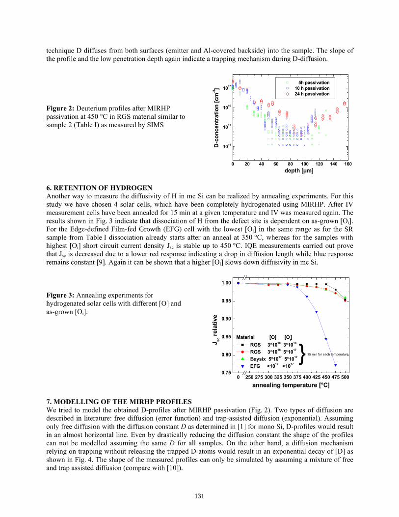
technique D diffuses from both surfaces (emitter and Al-covered backside) into the sample. The slope of the profile and the low penetration depth again indicate a trapping mechanism during D-diffusion. Figure 2: Deuterium profiles after MIRHP passivation at 450 °C in RGS material similar to sample 2 (Table I) as measured by SIMS
0 20 40 60 80 100 120 140 160
1014
1015
1016
1017 5h passivation 10 h passivation 24 h passivation
D-c
once
ntra
tion
[cm
-3]
depth [µm] 6. RETENTION OF HYDROGEN Another way to measure the diffusivity of H in mc Si can be realized by annealing experiments. For this study we have chosen 4 solar cells, which have been completely hydrogenated using MIRHP. After IV measurement cells have been annealed for 15 min at a given temperature and IV was measured again. The results shown in Fig. 3 indicate that dissociation of H from the defect site is dependent on as-grown [Oi]. For the Edge-defined Film-fed Growth (EFG) cell with the lowest [Oi] in the same range as for the SR sample from Table I dissociation already starts after an anneal at 350 °C, whereas for the samples with highest [Oi] short circuit current density Jsc is stable up to 450 °C. IQE measurements carried out prove that Jsc is decreased due to a lower red response indicating a drop in diffusion length while blue response remains constant [9]. Again it can be shown that a higher [Oi] slows down diffusivity in mc Si. Figure 3: Annealing experiments for hydrogenated solar cells with different [O] and as-grown [Oi].
0 250 275 300 325 350 375 400 425 450 475 5000.75
0.80
0.85
0.90
0.95
1.00
15 min for each temperatureMaterial [O] [Oi]
RGS 3*1018 3*1018
RGS 3*1018 5*1017
Baysix 5*1017 5*1017
EFG <1017 <1017
J sc re
lativ
e
annealing temperature [°C] 7. MODELLING OF THE MIRHP PROFILES We tried to model the obtained D-profiles after MIRHP passivation (Fig. 2). Two types of diffusion are described in literature: free diffusion (error function) and trap-assisted diffusion (exponential). Assuming only free diffusion with the diffusion constant D as determined in [1] for mono Si, D-profiles would result in an almost horizontal line. Even by drastically reducing the diffusion constant the shape of the profiles can not be modelled assuming the same D for all samples. On the other hand, a diffusion mechanism relying on trapping without releasing the trapped D-atoms would result in an exponential decay of [D] as shown in Fig. 4. The shape of the measured profiles can only be simulated by assuming a mixture of free and trap assisted diffusion (compare with [10]).
131

An empirical fit for a given set of diffusion parameters capture cross section R(H,X) of a trap X, trap concentration [X], concentration at the surface [H]0, and D in dependence of the depth x is shown in Fig. 4 by a superposition of the two diffusion mechanisms. Mean values and standard deviations are given as error bars for the points already shown in Fig. 2. The assumed effective diffusion constant at 450 °C of 7A10-11 cm2/s is several orders of magnitude lower than the one calculated from [1] (4A10-6 cm2/s). An explanation for this discrepancy can be given when the time is taken into account during which the D-atom is trapped. Together with the free diffusion between the release from one trap and the recapture at the next one an effective diffusion constant results which can be significantly lower as the one in defect free mono Si without trapping. Note that in the formula for the trap assisted diffusion only the product of R(H,X)A[X] is responsible for the shape of the profile. Figure 4: Empirical fits to the obtained MIRHP diffusion profiles (Fig. 2) with a set of diffusion parameters under the assumption of a mixture of trap-assisted and free diffusion with an effective diffusion constant D. Passivation times: 5 h (squares), 10 h (circles), 24 h (diamonds).
0 20 40 60 80 100 120 140 1601013
1014
1015
1016
1017 [ ] [ ] ( )[ ]( )xXXHRHH x ⋅−⋅= ,4exp0 π
[H]0=1.5e17 cm-3
R(H,X)=1e-21 cm[X]=1e18 cm-2
D=7e-11 cm2/sx24=200 µmx10=160 µmx5=170 µm
multiple trapping
free diffusion[ ] [ ]
⋅=
DtxerfcHH x 20
simulations multiple trapping free diffusion free + trapped diff. symmetric profile
conc
entr
atio
n [c
m-3]
depth [µm] 8. VACANCY CONCENTRATION It is known from literature that the concentration of vacancies might influence H-diffusivity in silicon. Vacancies can assist in cracking hydrogen molecules in atomic hydrogen [11], and a mechanism for an increased diffusivity of H via a vacancy-hydrogen complex has been discussed [12]. It could be assumed that there is a link between high [Oi] and low [vac]. Therefore, vacancy concentrations [vac] have been measured using the Pt method [13,14] to check if a low [vac] is responsible for the slowed down diffusion of H or D. [vac] as well as [Oi] and [Cs] (FTIR) for samples of Table I in the as-grown state (1, 3, and 4) and after POCl3 diffusion and SiN deposition (1-4, no firing) are shown in Table II. As-grown [vac] for the oxygen-rich RGS samples can be in the same range as measured for materials with low [Oi] like EFG [13], so [vac] is not a function of as-grown [Oi] alone. All RGS samples in the as-grown state reveal the same high [Cs]. A decrease in [vac] between the as-grown state and after POCl3 diffusion and SiN deposition is most pronounced when there is a reduction in [Oi] as well (sample 3). As a change in [Oi] is the result of O-precipitation during the high temperature diffusion step, it is important to take into account the mechanisms for O-precipitation. Precipitation rate of O is a function of both [Oi] as well as [Cs]. A high [Cs] as present in all RGS samples enhances O-precipitation as long as the overall [O] is not below a certain threshold in the range of 5A1017 cm-3 [15]. So the reduction in [vac] after diffusion can be explained by O-precipitation known to create self interstitials. On the other hand, hydrogen diffusion in EFG is much faster as in sample 2 despite of the same [vac] after POCl3 diffusion [13]. This indicates that hydrogen diffusivity is not directly linked to [vac]. Table II: [vac], [Oi], and [Cs] for samples listed in Table I and used for PECVD SIMS analysis in the as-grown state, and after POCl3 diffusion and SiN deposition.
as-grown after POCl3, SiN [vac]
[1012 cm-3][Oi]
[1018 cm-3][Cs]
[1018 cm-3][vac]
[1012 cm-3] [Oi]
[1018 cm-3] [Cs]
[1018 cm-3]1 <1 2.9 2.6 <1 0.4 0.9 2 <1 10 0.4 1.5 3 20 0.75 3.1 <1 0.3 2.7 4 20-50 0.3 2.7 20-30 0.3 2.8
132

9. DISCUSSION Deduced from the results presented above, a consistent model can be derived. H can be trapped at oxygen precipitates like New Donors formed in the temperature range between 600-900 °C where it is known to reduce recombination strength by passivation [16]. H (or D) can only be detected when O-precipitates exist in sufficient concentration. These are present mainly in samples 1, 2, and 3. Precipitates for sample 2 are larger because they are formed at higher temperatures (>1000 °C). Their concentration is therefore lower. As H might interact with the O-precipitate via its surface, the reduced surface area for precipitates in sample 2 (lower concentration of large precipitates with the same overall [O]) can be responsible for the faster diffusion as compared to sample 1. The larger the surface area of the precipitates, the more H can be trapped, and the measured profile gets steeper. If [Oi] in the as-grown state is below a certain concentration, O-precipitation at high temperatures is slowed down even in the presence of high [Cs]. This explains the strongly decreased [D] for samples 4 and 5. In this model the reduced H diffusivity in the bulk of materials with high [O] is not directly coupled with the [vac], but [vac] is influenced by precipitation of interstitial oxygen. A reduced [vac] due to generation of interstitials or absorption of vacancies during O-precipitation is therefore only an indirect marker of the reduced diffusivity of H. This does not question the ability of vacancies to create more atomic hydrogen by cracking H2 molecules, which might lead to a higher H-concentration, especially at the wafer surface. MIRHP passivation is generally applied in a lower temperature regime (300-450 °C). Here the retention of hydrogen at the traps is more pronounced as compared to hydrogenation via PECVD SiN and firing. Typical activation energies for dissociation of hydrogen from defects are in the range of 2-3 eV, corresponding to temperatures of around 400 °C [17]. Consideration of trapping is therefore even more important and can explain the steep profiles measured even after long passivation times. The reduced [Oi] led to lifetimes between 4-5 µs after hydrogenation in RGS wafers corresponding to sample 4 as compared to maximum values around 1 µs for hydrogenated wafers comparable with samples 1 and 2. In addition, this could be reached by reducing passivation time from >10 h to 1 h. 10. SUMMARY D-profiles after deposition and firing of a PECVD SiN layer could be presented in mc Si material. [D] and the shape of the profiles depend on oxygen concentration. Higher [D] and steeper profiles due to trapping are observed in material with large amount of O-precipitates, which could be shown by comparing [O], [Oi], [C], and [Cs] in the as-grown state and after emitter diffusion. [vac] itself seems not to play the leading role in hydrogen diffusion kinetics, but is strongly linked to O-precipitation. More details can be found in [17]. ACKNOWLEDGEMENTS We like to thank M. Stavola for stimulating discussions and A.M. Gabor for SR material supply. Part of this work was supported by the EC in the frame of the RGSells project (ENK6-CT2001-00574) and by the German BMU in the frame of the ASIS project (0329858J). REFERENCES [1] A. Van Wieringen, N. Warmoltz, Physica 22 (1956) 849 [2] M. Stavola, F. Jiang, A. Rohatgi, D. Kim, J. Holt, H. Atwater, J. Kalejs, Proc. 3rd WC PEC, Osaka 2003, 909 [3] M. Stavola, in Properties of Crystalline Si, edited by R. Hull (INSPEC, London, 1999) 511 [4] M. Spiegel, P. Fath, K. Peter, B. Buck, G. Willeke, E. Bucher, Proc. 13th EC PVSEC, Nizza 1995, 421 [5] V. Yelundur, A. Rohatgi, J.-W. Jeong, A.M. Gabor, J.I. Hanoka, R.L.Wallace, Proc. 28th IEEE PVSC, Anchorage 2000, 91 [6] G. Hahn, W. Jooss, M. Spiegel, P. Fath, G. Willeke, E. Bucher, Proc. 26th IEEE PVSC, Anaheim 1997, 75 [7] H.F.W. Dekkers et al., Proc. 3rd WC PEC, Osaka 2003, 983 [8] G. Hahn, P. Geiger, P. Fath, E. Bucher, Proc. 28th IEEE PVSC, Anchorage 2000, 95 [9] T. Pernau, G. Hahn, M. Spiegel, G. Dietsche, Proc. 17th EC PVSEC, Munich 2001, 1764 [10] B.L. Sopori, Y. Zhang, R. Reedy, Proc. 29th IEEE PVSC, New Orleans 2002, 222 [11] S.K. Estreicher, J.L Hastings, P.A. Fedders, Phys. Rev. B 57(20) (1998) R12 663 [12] B.L. Sopori et al., Solar Energy Materials and Solar Cells 41/42 (1996) 159 [13] D. Karg, G. Pensl, M. Schulz, Proc. 3rd WC PEC, Osaka 2003, 1112 [14] D. Karg, H. Charifi, G. Pensl, M. Schulz, G. Hahn, Proc. 19th EC PVSEC, Paris 2004, in press [15] Q. Sun, K.H. Yao, J. Lagowski, H.C. Gatos, J. Appl. Phys. 67(9) (1990) 4313 [16] D. Karg, A. Voigt, J. Krinke, C. Hässler, H.-U. Höfs, G. Pensl, M. Schulz, H.P. Strunk, Solid State Phenomena 67-68 (1999) 33 [17] H.J. Möller, Semiconductors for Solar Cells (Artech House, Boston, 1993) 148 [18] G. Hahn et al., Proc. 19th EC PVSEC Paris, in press
133

Introduction of H into Si as Characterized by IR Spectroscopy M. Stavola, W. Tang, and F. Jiang Department of Physics, Lehigh University, Bethlehem, Pennsylvania 18015 V. Yelundur and A. Rohatgi School of Electrical Engineering, Georgia Institute of Technology, Atlanta, Georgia 30332 G. Hahn University of Konstanz, Department of Physics, PO Box X916, 78457 Konstanz, Germany J. Kalejs, RWE Schott Solar, Inc., Billerica, Massachusetts 01821 Abstract: The hydrogenation of Si by methods used to passivate defects in Si solar cells has been studied by IR spectroscopy. Floating-zone Si that contained Pt impurities that act as traps for H was used as a model system for these studies. H was directly detected, allowing its concentration and indiffusion depth to be estimated. A progress report on experiments that compare the effectiveness of different hydrogenation treatments is presented. I. Introduction Hydrogen is commonly introduced into Si solar cells to reduce the deleterious effects of defects and to increase cell efficiency [1-8]. Nonetheless, the methods by which hydrogen is introduced during processing and hydrogen’s subsequent interactions with defects remain poorly understood. Typically, the direct detection of H by methods such as secondary ion mass spectrometry (SIMS) is not possible, even when D is used instead of H to improve the detection limit, because of hydrogen’s small concentration [9]. Therefore, the concentration of H that is introduced is not known and the effect that changes in processing methods have on the effectiveness of hydrogenation is difficult to access. Furthermore, the indiffusion of H into Si is often limited by trapping, making the appropriate diffusion constant to describe the penetration depth of H uncertain [10]. In our studies, floating-zone Si that contains Pt impurities is used as a model system to study the introduction of H by processes typically used to fabricate solar cells. A novel method that combines infrared (IR) spectroscopy with Pt marker impurities that can trap H in Si is used to determine the concentration and depth of H [11]. Pt impurities are used as traps in our experi-ments because the Pt-H complexes in Si do not dissociate up to an annealing temperature of 650ºC and their H vibrational lines have been identified [12]. The intensities of the PtH IR lines have also been calibrated so that the concentration of H in the Si samples can be estimated [13]. It has also been proposed that the Si vacancy might play a role during hydrogenation processes [8]. Vacancy-H complexes have been studied previously by IR spectroscopy [14, 15], which has
134

made it possible for us to detect the presence of vacancies that have been introduced into our Si samples during hydrogenation treatments. The present paper is a progress report on our work to compare the introduction of hydrogen from SiNx layers deposited and processed by different methods. The hydrogenation of Si from a microwave-induced remote hydrogen plasma [16] has also been investigated.
II. Experiment Pt impurities, to be used as traps for H, were diffused into the Si samples at a temperature of 1225°C. The resulting Pt concentration is estimated to be ~1017 cm-3 from solubility data in the literature [17]. SiNx layers were deposited onto several Si samples either by plasma-enhanced chemical vapor deposition (PECVD) [5,6] or by hot-wire chemical vapor deposition (HWCVD) [18]. The substrate temperature for the depositions was ~300°C and the nitride layer thicknesses were ~80 to 100 nm. PECVD SiNx films deposited in 50 kHz and 13.6MHz reactors were also compared. Al films were evaporated onto the back side of a few samples to investigate the effect of cofiring an Al back contact on the effectiveness of the hydrogenation. A few samples were also hydrogenated with a microwave-induced remote hydrogen plasma [16]. In this case, a flow of H2 was passed through a cavity, and a microwave generator (2.45 GHz, 75 W) was used to excite the plasma. Samples were placed downstream and also were not exposed to UV light from the plasma. In this case, H was introduced at a sample temperature of 350ºC for exposure times up to 10 h. IR absorption measurements have been made for samples in a multiple-internal-reflection (MIR) geometry in order to increase the sensitivity of vibrational spectroscopy for the detection of small concentrations of H-containing defects,. Samples with dimensions 15 x 18 x1.5 mm3 were made from lightly doped Si grown by the floating-zone method. The ends of the samples were beveled at 45º. The probing light was introduced through one of the beveled ends so as to be multiply reflected many times from the internal surfaces as it passes through the sample (Fig. 1). IR absorption measurements were made with a Bomem DA3 FTIR spectrometer equipped with a KBr beamsplitter and an InSb detector. Samples were cooled for IR measurements to near 4.2K with a Helitran, continuous-flow cryostat. It was found that the presence of an Al back-contact layer that was present for some of our experiments greatly reduced the transmission of the Si samples. After samples were annealed to introduce H, the Al layer was removed by lapping and polishing prior to subsequent IR measurements.
III. Experimental Results IR spectra are shown in Fig. 2 for a Si:Pt sample onto which a SiNx layer had been deposited by HWCVD. The broad band centered at 2160 cm-1 is due to Si-H bonds in the H-rich SiNx layer. For anneals performed at successively higher temperatures, the Si-H band from the SiNx decreases in intensity and an H vibrational line at 1880 cm-1, assigned previously to the neutral charge state of the PtH complex in Si [12], grows in intensity. The intensity of the PtH IR line at 1880 cm-1 provides quantitative information about the concentration of H in the Si sample. From the calibration of the intensity of the PtH line
135
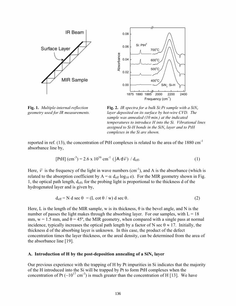
reported in ref. (13), the concentration of PtH complexes is related to the area of the 1880 cm-1 absorbance line by, [PtH] (cm-3) = 2.6 x 1016 cm-1 )(∫ νdA / deff. (1) Here, ν is the frequency of the light in wave numbers (cm-1), and A is the absorbance (which is related to the absorption coefficient by A = α deff log10 e). For the MIR geometry shown in Fig. 1, the optical path length, deff, for the probing light is proportional to the thickness d of the hydrogenated layer and is given by, deff = N d sec θ = (L cot θ / w) d sec θ. (2) Here, L is the length of the MIR sample, w is its thickness, θ is the bevel angle, and N is the number of passes the light makes through the absorbing layer. For our samples, with L = 18 mm, w = 1.5 mm, and θ = 45º, the MIR geometry, when compared with a single pass at normal incidence, typically increases the optical path length by a factor of N sec θ ≈ 17. Initially, the thickness d of the absorbing layer is unknown. In this case, the product of the defect concentration times the layer thickness, or the areal density, can be determined from the area of the absorbance line [19].
A. Introduction of H by the post-deposition annealing of a SiNx layer Our previous experience with the trapping of H by Pt impurities in Si indicates that the majority of the H introduced into the Si will be trapped by Pt to form PtH complexes when the concentration of Pt (~1017 cm-3) is much greater than the concentration of H [13]. We have
Fig. 1. Multiple-internal-reflection geometry used for IR measurements.
1875 1880 1885 2000 2200 2400
0.00
0.02
0.04
0.06
0.08
SiNx: Si-H
Si: PtH0
400oC
500oC
600oC
700oC
Abs
orba
nce
Frequency (cm-1)
Fig. 2. IR spectra for a bulk Si:Pt sample with a SiNx layer deposited on its surface by hot-wire CVD. The sample was annealed (10 min.) at the indicated temperatures to introduce H into the Si. Vibrational lines assigned to Si-H bonds in the SiNx layer and to PtH complexes in the Si are shown.
136

found this to be the typical situation when hydrogen is introduced from a SiNx layer [11] (a conclusion that is also consistent with the results of SIMS studies which find H to be below the detection limit for samples hydrogenated from SiNx layers [9]). Therefore, the concentration of PtH complexes reflects the total concentration of H introduced into the Si from the SiNx layer. The introduction of H into Si by the post-deposition annealing of a SiNx layer has been investigated for different deposition methods, annealing treatments [furnace or rapid thermal process (RTP)], and, in a few cases, with an evaporated Al back-contact layer present. A summary of the results of these experiments is shown in Table I. We emphasize that these are first results for a small number of samples, and the trends that are observed should be considered with caution [20]. Furthermore, only a few experiments have been done to optimize the annealing treatments that introduce H. (For example, we have found that increasing the annealing time of a furnace anneal at 600ºC from 10 min to 30 min increases the areal density of PtH by a factor of 1.5.) Table I. Results for the introduction of H into Si from an annealed SiNx layer. Deposition method, sample characteristics, annealing treatment, and the areal density of PtH complexes as determined from the area of the 1880 cm-1 vibrational line assigned to PtH0.
SiNx deposition Sample Treatment PtH areal density
(cm-2) PECVD (50 kHz) p-Si:Pt 600ºC, 15 min 2.4 x 10¹² PECVD (50 kHz) p-Si:Pt w/Al 600ºC, 20 min 1.2 x 10¹² PECVD (50 kHz) p-Si:Pt 750ºC, RTP, 1 min 4.0 x 10¹² PECVD (50 kHz) p-Si:Pt w/Al 750ºC, RTP, 1 min 2.8 x 10¹² PECVD (13.6 MHz) p-Si:Pt 600ºC, 5 min 0.46 x 10¹² PECVD (13.6 MHz) p-Si:Pt 700ºC, RTP, 1 min 0.36 x 10¹² HWCVD p-Si:Pt 600ºC, 10 min 5.8 x 10¹²
If we compare the results obtained for different SiNx deposition methods, HWCVD provided the most effective hydrogenation of Pt impurities in the Si. SiNx films produced by PECVD in a 50 kHz reactor were nearly as effective at introducing H. Results for SiNx films produced by PECVD in a 13.6 MHz reactor introduced significantly less H into the Si than the films produced by HWCVD or in the low frequency reactor. Rapid thermal processing with brief anneals (1 min) at 750ºC was somewhat more effective for hydrogenating Pt impurities in our samples than longer furnace anneals at 600ºC. We expect that the rapid cool down associated with RTP might be even more important for defects whose hydrogenation is less thermally stable than that of Pt. It has been suggested that the co-firing of a SiNx front surface layer with an Al back contact leads to greater defect passivation [6,7,21]. Our results do not show more effective hydrogenation for samples with an Al back contact layer either for furnace annealing or RTP.
137
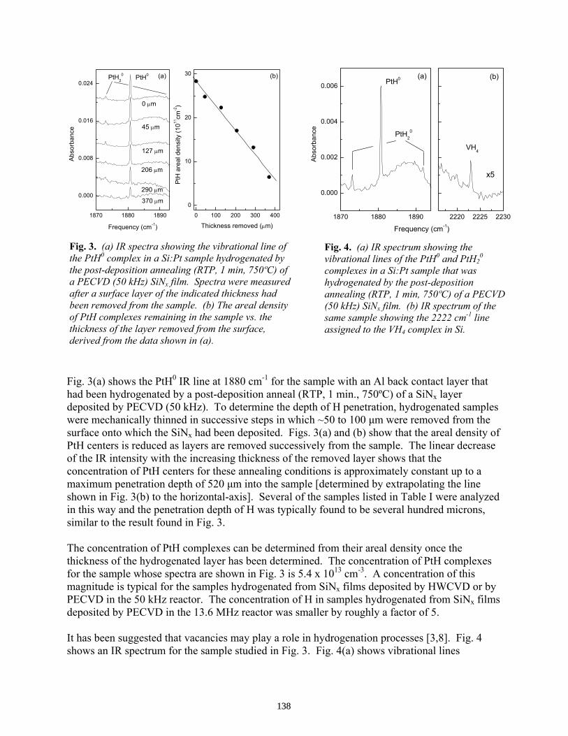
Fig. 3(a) shows the PtH0 IR line at 1880 cm-1 for the sample with an Al back contact layer that had been hydrogenated by a post-deposition anneal (RTP, 1 min., 750ºC) of a SiNx layer deposited by PECVD (50 kHz). To determine the depth of H penetration, hydrogenated samples were mechanically thinned in successive steps in which ~50 to 100 µm were removed from the surface onto which the SiNx had been deposited. Figs. 3(a) and (b) show that the areal density of PtH centers is reduced as layers are removed successively from the sample. The linear decrease of the IR intensity with the increasing thickness of the removed layer shows that the concentration of PtH centers for these annealing conditions is approximately constant up to a maximum penetration depth of 520 µm into the sample [determined by extrapolating the line shown in Fig. 3(b) to the horizontal-axis]. Several of the samples listed in Table I were analyzed in this way and the penetration depth of H was typically found to be several hundred microns, similar to the result found in Fig. 3. The concentration of PtH complexes can be determined from their areal density once the thickness of the hydrogenated layer has been determined. The concentration of PtH complexes for the sample whose spectra are shown in Fig. 3 is 5.4 x 1013 cm-3. A concentration of this magnitude is typical for the samples hydrogenated from SiNx films deposited by HWCVD or by PECVD in the 50 kHz reactor. The concentration of H in samples hydrogenated from SiNx films deposited by PECVD in the 13.6 MHz reactor was smaller by roughly a factor of 5. It has been suggested that vacancies may play a role in hydrogenation processes [3,8]. Fig. 4 shows an IR spectrum for the sample studied in Fig. 3. Fig. 4(a) shows vibrational lines
1870 1880 1890
0.000
0.008
0.016
0.024
0 100 200 300 400
0
10
20
30PtH20 PtH0
370 µm
290 µm
206 µm
127 µm
45 µm
0 µm
(a)
Abso
rban
ce
Frequency (cm-1)
(b)
PtH
are
al d
ensi
ty (1
011cm
-2)
Thickness removed (µm)1870 1880 1890
0.000
0.002
0.004
0.006
2220 2225 2230
(a)
PtH20
PtH0
Abs
orba
nce
Frequency (cm-1)
(b)
x5
VH4
Fig. 4. (a) IR spectrum showing the vibrational lines of the PtH0 and PtH2
0 complexes in a Si:Pt sample that was hydrogenated by the post-deposition annealing (RTP, 1 min, 750ºC) of a PECVD (50 kHz) SiNx film. (b) IR spectrum of the same sample showing the 2222 cm-1 line assigned to the VH4 complex in Si.
Fig. 3. (a) IR spectra showing the vibrational line of the PtH0 complex in a Si:Pt sample hydrogenated by the post-deposition annealing (RTP, 1 min, 750ºC) of a PECVD (50 kHz) SiNx film. Spectra were measured after a surface layer of the indicated thickness had been removed from the sample. (b) The areal density of PtH complexes remaining in the sample vs. the thickness of the layer removed from the surface, derived from the data shown in (a).
138

associated with the PtH0 and PtH2
0 complexes in Si. Fig. 4(b) shows a weak vibrational line at 2222 cm-1 that has been unambiguously assigned to the VH4 complex [14,15]. This observation shows that hydrogenated vacancies are indeed present in the sample. (This IR line was observed in both of the samples annealed by RTP but not in furnace annealed samples.) Unfortunately, only a very rough calibration of the IR intensity of the 2222 cm-1 line has been reported [22]. This approximate calibration of the 2222 cm-1 line leads to an estimate of the vacancy concentration in the sample of ~ 5 x 1012 cm-3. This estimate could easily be in error by a factor of 10 or more. Nonetheless, hydrogenated vacancies are directly observed in these experiments. The possible role of vacancies in hydrogenation processes remains uncertain.
B. Introduction of H from a microwave-induced remote hydrogen plasma A few samples were hydrogenated from a hydrogen-plasma for our experiments. Spectra for a Si:Pt sample hydrogenated for 10 hr at 350ºC are shown in Fig. 5. Vibrational lines assigned to the PtH0 and PtH2
0 are shown in Fig. 5(a). Prominent vibrational lines assigned previously to the VH4 and V2H6 complexes [14,15] are seen in Fig. 5(b), establishing the presence of vacancies (and divacancies) in the sample. VH4 and V2H6 are the vacancy-H complexes that are thermally stable at 350ºC [14], the temperature at which H was introduced. Figs. 6 and 7 show IR spectra for the PtHn and VH4 complexes as Si layers were removed successively from the sample. Fig. 6 shows that the areal density of PtH0 complexes (2.3 x 1012 cm-2) is comparable to samples hydrogenated from a SiNx layer but that these complexes are present in a thin layer (~ 35 µm thick) at the sample surface. The local concentration of PtH complexes is therefore larger in this case (~ 8 x 1014 cm-3). The greater local concentration of H in a thin layer explains why the relative intensity of the IR lines due to PtH2
0 has increased compared to the result shown in Fig. 4 for a sample hydrogenated from a SiNx layer. For the greater local concentration of H in the plasma-treated samples, a substantial concentration of H is also present in the defect complexes VH4 and V2H6. We have used a rough calibration [22] of the IR intensity of the line at 2222 cm-1 to estimate the areal density of H associated with the VH4 complex. In this case, the areal density of H associated with VH4 is
Fig. 5. IR spectra for a Si:Pt sample hydrogenated by exposure to a remote hydrogen plasma (350ºC, 10 hr). The spectrum in (a) shows the IR lines assigned to the PtH0 and PtH2
0 complexes. The spectrum in (b) shows IR lines assigned to the VH4 and V2H6 complexes in Si.
1870 1875 1880 1885 1890 1895
0.000
0.002
0.004
2160 2180 2200 2220
(a)PtH2
0
PtH0
Abso
rban
ce
Frequency (cm-1)
(b)V2H6 VH4
139

estimated to be 24 x 1012 cm-2. These defects are present in a layer ≤ 35 µm thick leading to a local H concentration of ~7 x 1015cm-3, i.e., roughly 10 times greater than the H concentration associated with PtH centers. Presumably, the concentration of V2H6 defects is comparable, but given the crudeness of our estimates, we do not attempt further analysis. H may also be present in the plasma-treated samples in the form of other defects that we have not detected. Vacancies associated with VH4 have an estimated concentration of one-fourth the corresponding H concentration, or ~2 x 1015 cm-3.
IV. Diffusivity of H during hydrogenation treatments The diffusivity of H in Si was measured at high temperature in an early study by Van Wieringen and Warmoltz [23] and gives the diffusion constant,
DH = 9.4 x 10⁻³ exp(-0.48 eV / kT) cm2/s. (3)
Subsequent studies have found that the DH given by Eq. (3) is valid for the diffusion of H+, the dominant charge state of H in Si at elevated temperature [24], for situations where H does not interact with other defects and where relatively immobile H2 molecules are not formed [10]. In many experimental situations, the diffusion of H is limited by trapping, and an effective diffusion constant is found that is typically two to three orders of magnitude smaller than Eq. (3) would predict [10]. Therefore, it becomes important to obtain data on the indiffusion depth of H that are valid for specific hydrogenation conditions.
1870 1875 1880 1885 1890
0.000
0.004
0.008
0.012
0 50 100 150 200
0
5
10
15
20
25(a) PtH2
0
PtH0
180 µm
125 µm
76 µm
29 µm
0 µm
A
bsor
banc
e
Frequency (cm-1)
(b)
PtH20
PtH0
Are
al d
ensi
ty (1
011cm
-2)
Thickness removed (µm)
Fig. 6. (a) IR spectra showing the vibrational lines of the PtH0 and PtH2
0 complexes in a Si:Pt sample hydrogenated by exposure to a hydrogen plasma (350ºC, 10 hr). Spectra were measured after a surface layer of the indicated thickness had been removed from the sample. (b) The areal density of PtH0 and PtH2
0 complexes remaining in the sample vs. the thickness of the layer removed from the surface, derived from the data shown in (a).
Fig. 7. (a) IR spectra showing the vibrational line of the VH4 complex in a Si:Pt sample hydrogenated by exposure to a hydrogen plasma (350ºC, 10 hr). Spectra were measured after a surface layer of the indicated thickness had been removed from the sample. (b) The areal density of H associated with the VH4 complexes remaining in the sample vs. the thickness of the layer removed from the surface, derived from the data shown in (a).
2220 2225 2230
0.000
0.004
0.008
0.012
0 50 100 150
0
50
100
150
200(a)VH4
180 µm
125 µm
76 µm
29 µm
0 µm
Abs
orba
nce
Frequency (cm-1)
(b)VH4
Area
l den
sity
(1011
cm-2)
Thickness removed (µm)
140

Previous results for the hydrogenation of Si from SiNx layers annealed at 600 and 700ºC were consistent with the diffusivity given by Eq. (3) [11]. Similarly, the results obtained in the present experiments for samples hydrogenated from SiNx layers are consistent with the rapid indiffusion of H predicted by Eq. (3). For example, the diffusivity given by Eq. (3) at 750ºC is DH(750ºC) = 4.1 x 10⁻⁵ cm2/s. For a 1 min anneal at 750ºC, this value predicts a √(Dt) diffusion length of 490 µm which is close to the penetration depth of H found in experiments reported here [~520 µm from the data shown in Fig. 3(b)]. Our experimental results for Si:Pt hydrogenated from a hydrogen plasma at 350ºC show an effective diffusivity that is more than 1000 times smaller than the value given by Eq. (3). From Eq. (3), one obtains a diffusivity at 350ºC of DH(350ºC) = 1.2 x 10⁻⁶ cm2/s. For the plasma exposure of 10 hrs used in our experiments, this diffusivity would predict a √(Dt) diffusion length of 2100 µm. The penetration depth of H found in our experiments [Fig. 7(b)] is only 35 µm and is consistent with an effective diffusivity of ~3 x 10⁻¹⁰ cm2/s. Similar values of Deff have been found in a variety of hydrogen diffusion experiments and are typical of trap limited diffusion [11]. The different values observed for the penetration depth of H for hydrogenation treatments conducted near 700ºC from a SiNx layer and near 350ºC from a hydrogen plasma demonstrate an important difference between these hydrogenation methods. We note that the values of the H penetration depth and the corresponding Deff obtained in our experiments may depend on the concentration and stability of hydrogen traps in the sample and that our results which are valid for the model system we have chosen (FZ Si:Pt) may not necessarily apply in other situations. Nonetheless, the ability of hydrogenation treatments performed by the annealing of SiNx layers to hydrogenate thick layers of Si is well matched to requirements of solar-cell passivation processes.
V. Conclusion Spectroscopic studies of the hydrogenation of floating-zone Si that contained Pt impurities (which act as traps for H) provide new insights into the concentration and penetration depth of H introduced from annealed SiNx layers and from a hydrogen plasma.
VI. Acknowledgments We thank Jason Holt and Harry Atwater for a collaboration that led to the results obtained for SiNx layers deposited by HWCVD. We thank Stefan Estreicher for numerous helpful discussions. This work was supported by NREL grant AAT-1-31605-04.
References 1. C. H. Seager, D. S. Ginley, and J. D. Zook, Appl. Phys. Lett. 36, 831 (1980). 2. J.I. Hanoka, C.H. Seager, D.J. Sharp, and J.K.G. Panitz, Appl. Phys. Lett. 42, 618 (1983). 3. B.L. Sopori, X. Den, J.P. Benner, A. Rohatgi, P. Sana, S.K. Estreicher, Y.K. Park, and M.A. Roberson, Solar Energy Materials and Solar Cells 41/42, 159 (1996).
141
4. A. Rohatgi, P. Doshi, J. Moschner, T. Lauinger, A.G. Aberle, and D.S. Ruby, IEEE Trans. Electron. Dev. 47, 987 (2000). 5. A. G. Aberle, Sol. Energy Mater. Sol. Cells 65, 239 (2001) reviews the SiNx passivation of c-Si solar cells and includes a historical overview. 6. F. Duerinckx and J. Szlufcik, Sol. Energy Mater. Sol. Cells 72, 231 (2002). 7. A. Cuevas, M.J. Kerr, and J. Schmidt, Proc. 3rd World Conf. on Photovoltaic Energy Conversion, Osaka, 2003. 8. B. L. Sopori, Y. Zhang, and R. Reedy, Proc. 29th IEEE-Photovoltaic Specialists Conference, New Orleans, May 2002, edited by R. D. McConnell (Report No. NREL/EL-590-32461). 9. H.F.W. Dekkers, S. DeWolf, G. Agostinelli, J. Szlufcik, T. Pernau, W.M. Arnoldbik, H.D. Goldbach, R.E.I. Schropp. Proc. 3rd World Conf. on Photovoltaic Energy Conversion, Osaka, 2003. 10. M. Stavola, in Properties of Crystalline Si, edited by R. Hull (INSPEC, London, 1999), p. 511. 11. F. Jiang, M. Stavola, A. Rohatgi, D. Kim, J. Holt, H. Atwater, J. Kalejs, Appl. Phys. Lett. 83, 931 (2003). 12. S.J. Uftring, M. Stavola, P.M. Williams, and G.D. Watkins, Phys. Rev. B 51, 9612 (1995)l 13. M.G. Weinstein, M. Stavola, K.L. Stavola, S.J. Uftring, J. Weber, J.-U. Sachse, and H. Lemke, Phys. Rev. B 65, 035206 (2002). 14. B. Bech Nielsen, L. Hoffman, M. Budde, R. Jones, J. Goss, and S. Öberg, Mat. Sci. Forum 196-201, 933 (1995). 15. B. Bech Nielsen, L. Hoffman, and M. Budde, Mat. Sci. Eng. B 36, 259 (1996). 16. M. Spiegel, P. Fath, K. Peter, B. Buck, G. Willeke, E. Bucher, Proc. 13th EC PVSEC, Nizza, 1995, p. 421. 17. Impurities and Defects in Group IV Elements and III-V Compounds, Vol. III/22b, in the Landolt-Bornstein, New Series, edited by O. Madelung and M. Schulz (Springer, Berlin, 1989). 18. J.K. Holt, D.G. Goodwin, A.M. Gabor, F. Jiang, M. Stavola, and H.A. Atwater, Thin Solid Films 430, 37 (2003). 19. The integrated absorption coefficient is proportional to the concentration of absorbing centers. However, the absorbance, A, determined by experiment, is proportional to the product of the absorption coefficient times the thickness of the absorbing layer. The integrated absorbance, therefore, is proportional to the concentration of centers times the thickness of the absorbing layer, that is, to the areal density. 20. While we have worked to eliminate artifacts from our measurements, this is a novel characterization method, and all problems may not yet have been solved. The two samples that were annealed by RTP showed anomalously large PtH IR lines upon first measurements that were reduced to the values given in Table I when the front surface was repolished. The presence of possible artifacts in our measurements continues to be investigated. 21. V. Yelundur, A. Rohatgi, A. Ebong, A.M. Gabor, J. Hanoka, and R.L. Wallace, J. Electron. Mater. 30, 526 (2001). 22. L. Hoffman, E.V. Lavrov, and B. Bech Nielsen, Mat. Sci. Engr. B 58, 167 (1999), have estimated an effective oscillating charge of q = 0.3e per H atom for the VHn complexes in Si. 23. A. Van Wieringen, and N. Warmoltz, Physica 22, 849 (1956). 24. C. Herring, N. M. Johnson and C. G. Van de Walle, Phys. Rev. B 64, 125209 (2001).
142

Characterisation of Multi-Crystalline Blocks and Efforts to Relate Their Properties to the Efficiencies of Solar Cells
L. J. Geerligs
ECN Solar Energy, PO Box 1, NL-1755 ZG Petten, The Netherlands Abstract: We present characterisation results of current standard quality multicrystalline ingots, with the objective to relate the material quality to the solar cell performance. Interstitial iron (Fei) and oxygen concentrations and crystallographic defect density are among the most useful parameters. The use and interpretation of measurements of interstitial iron content in multicrystalline silicon is discussed in some detail. Fei is generally the most important impurity and lifetime measurements become more predictive and applicable when quantitatively separating the lifetime due to Fei from lifetime due to other defects. In addition, because of its convenient measurement, Fei is a convenient probe to evaluate and model the effect of high-temperature steps. Introduction The properties of solar cells produced from multicrystalline silicon (mc-Si) wafers show a significant variation. It is useful to understand the part of this variation which is due to material properties, and to see whether the understanding can be generic, independent of manufacturer. In this paper we will look at current standard quality ingot-grown mc-Si. A characterization of commonly used mc-Si can help to put studies which focus on special material with for example high concentrations of a particular kind of defect into context. Multicrystalline silicon (mc-Si) for solar cells is commonly grown in large rectangular ingots, which are solidified from bottom to top. These ingots are cut into vertical ‘bricks’ or 'columns' of square cross-section, which are subsequently cut into wafers. The material parameters of the ingots vary from bottom to top, as well as laterally, depending on equipment, materials and procedures used by the manufacturers. It has been a long-standing goal to develop a quick screening of as-grown material which predicts the solar cell properties. As a rudimentary screening, manufacturers measure
the lifetime on blocks, before wafering, to determine which part of the block can be sold as wafers, and which part should be recycled or discarded. Measuring some more parameters can improve the usefulness of this screening. Only using the lifetime criterium may in fact result in discarding more material than necessary. Hence, a better understanding of the relation between material parameters and cell performance is valuable in several respects: - By determining more exactly which material will result in acceptable cells, the yield from mc-Si ingot growth may be increased. - It will be clearer which growth parameters form a bottleneck for cell performance and need to be improved (e.g., feedstock purity, or cool down rate). - If it is clear which material parameters are responsible for cell degradation, and how these material parameters vary through an ingot, it should be possible to adapt process parameters in a production line to the part of an ingot that is momentarily processed. Parameters which turn out to be useful are: - the concentration of dissolved iron (Fei) - the concentration of dissolved oxygen (Oi) - the defect and lifetime distribution (i.e., the distribution of low defect, high lifetime areas versus high defect, low lifetime areas over the wafer). In this paper, all three parameters are found to be necessary to qualitatively explain the response of wafers to cell processing and the resulting cell efficiencies. The defect/lifetime distribution seems to be the main parameter for the variation of cell efficiency within most of the ingot volume (in some cases excluding some of the edge regions). The quantitative prediction of variation of cell efficiency between ingots will probably depend on microscopic parameters, such as decoration of dislocations, or presence of impurities other than Fe, additional to the three
143
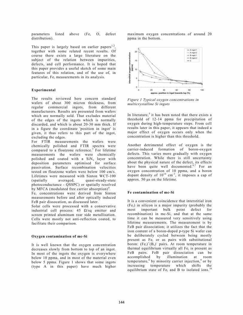
parameters listed above (Fe, O, defect distribution). This paper is largely based on earlier papers1,2, together with some related recent results. Of course there exists a large literature on the subject of the relation between impurities, defects, and cell performance. It is hoped that this paper provides a useful sketch of some main features of this relation, and of the use of, in particular, Fei measurements in its analysis. Experimental The results reviewed here concern standard wafers of about 300 micron thickness, from regular commercial ingots, from different manufacturers. Results are presented from wafers which are normally sold. That excludes material of the edges of the ingots which is normally discarded, and which is about 20-30 mm thick. If in a figure the coordinate 'position in ingot' is given, it thus refers to this part of the ingot, excluding the edges. For FTIR measurements the wafers were chemically polished and FTIR spectra were compared to a floatzone reference.3 For lifetime measurements the wafers were chemically polished and coated with a SiNx layer with deposition parameters optimised for surface passivation. Surface recombination velocities tested on floatzone wafers were below 100 cm/s. Lifetimes were measured with Sinton WCT-100 (spatially averaged, quasi-steady-state photoconductance - QSSPC) or spatially resolved by MFCA (modulated free carrier absorption)4. Fei concentrations were derived from Sinton measurements before and after optically induced FeB pair dissocation, as discussed later. Solar cells were processed with a conservative industrial cell process: 45 Ω/sq emitter and screen printed aluminum rear side metallisation. Cells were mostly not anti-reflection coated, to facilitate their comparison. Oxygen contamination of mc-Si It is well known that the oxygen concentration decreases slowly from bottom to top of an ingot. In most of the ingots the oxygen is everywhere below 10 ppma, and in most of the material even below 5 ppma. Figure 1 shows that some ingots (type A in this paper) have much higher
maximum oxygen concentrations of around 20 ppma in the bottom.
0
5
10
15
20
0 20 40 60 80 100approx. position in ingot towards top (%)
inte
rstit
ial o
xyge
n co
ncen
trat
ion
(ppm
a)
A ingot 1A ingot 2B ingot 1B ingot 2C
Figure 1 Typical oxygen concentrations in multicrystalline Si ingots
In literature,5 it has been noted that there exists a threshold of 12-14 ppma for precipitation of oxygen during high-temperature steps. From cell results later in this paper, it appears that indeed a major effect of oxygen occurs only when the concentration is higher than this threshold. Another detrimental effect of oxygen is the carrier-induced formation of boron-oxygen defects. This varies more gradually with oxygen concentration. While there is still uncertainty about the physical nature of the defect, its effects have been quite well documented.6,7 For an oxygen concentration of 10 ppma, and a boron dopant density of 1016 cm-3, it imposes a cap of approx. 50 µs on the lifetime. Fe contamination of mc-Si It is a convenient coincidence that interstitial iron (Fei) in silicon is a major impurity (probably the most important bulk point defect for recombination) in mc-Si, and that at the same time it can be measured very sensitively using lifetime measurements. The measurement is by FeB pair dissociation; it utilizes the fact that the iron content of a boron-doped p-type Si wafer can be deliberately cycled between being mostly present as Fei or as pairs with substitutional boron: (Fei)+(Bs)- pairs. At room temperature in thermal equilibrium virtually all Fei is present as FeB pairs. FeB pair dissociation can be accomplished by illumination at room temperature,8 by minority carrier injection,9 or by increasing temperature which shifts the equilibrium state of Fei and B to isolated ions.10
144

The isolated and paired form of interstitial iron have markedly different recombination properties.11,12 This leads to significant changes in carrier lifetime and diffusion length after dissociating the FeB pairs. Assuming that all other recombination processes remain unchanged, the FeB concentration can be found by measuring the carrier lifetime before (τ0) and after (τ1) pair dissociation: [FeB]=C(τ1
-1-τ0-1). The use of the
known recombination parameters of both FeB pairs and Fei provides the pre-factor C.11,12,13 Calculating FeB concentrations from geometrically averaged lifetimes (such as determined with the Sinton WCT-100) can result in an overestimate. This happens when the lifetime measurement averages over areas of low and high lifetime, with the same concentration of FeB. Typical errors are estimated to be up to a factor 2. Details will be given in ref.14
1.E+11
1.E+12
1.E+13
1.E+14
0 20 40 60 80 100approx. position in ingot, towards top (%)
[FeB
] in
cm-3
A ingot 1
A ingot 2
B ingot 1
B ingot 2
C
Figure 2 FeB in mc-Si ingots.
0.0E+00
5.0E+11
1.0E+12
1.5E+12
2.0E+12
0 20 40 60approx. position in block from bottom (mm)
[FeB
] in
cm-3
A ingot 2
Figure 3. Detailed FeB measurements in the bottom of ingot A2.
Figure 2 shows FeB concentrations measured for a number of ingots. Figure 3 shows a detail for the bottom 100 mm of one particular ingot. The central parts (20-80% of ingot height) of the
ingots show qualitatively different properties than the edges. This is due to different mechanisms for the incorporation of Fei. 1) In the central parts, take-up is from contamination in the liquid silicon during solidification. This is governed by the process of segregation: only a small fraction (~10-4) of the concentration in the liquid state is incorporated as Fei in the solid state. Because the impurities are concentrated in the liquid silicon as solidification progresses, the concentration of Fei increases towards the top of the ingot. Most of the concentrated impurities precipitate in the final stage of solidification, in the very top of the ingot. The amount of Fei in the central part of the ingots is about 1-3·1011 cm-3, or about 0.05 ppba. The equilibrium segregation coefficient of Fe between solid and liquid silicon is just below 10-5, and would apply for infinitely slow ingot growth The real segregation coefficient is probably higher by approx. a factor 10, i.e. around 10-4.15 This indicates that the typical contamination of the melt with iron is of order 0.5 ppma. 2) In the edges, most Fei originates from solid-state diffusion after solidification.16 This gives rise to the increased FeB concentration; between 1012 and 1013 cm-3 at approx. 2-3 cm distance from the edges. For bottom and side edges, the source must be the crucible or crucible coating. In the top edge, the impurities have diffused back into the ingot from the precipitated layer of the final stage of solidification. The source of iron may in fact be partly the same in both cases: The Fe diffusing from crucible/coating into the solidified ingot will also dissolve into the liquid silicon before solidification. Together with Fe impurities already present in the silicon feedstock, this gives rise to at least part of the Fei in the central parts of the ingots. Figure 4 shows the lifetime and FeB profiles of one particular column. It is remarkable how well the lifetime follows the (inverse) trend of the FeB. There are potentially other impurities present in the crucible or coating material. However, these will generally have diffusivities very different from Fe, and will therefore diffuse to a different depth than the Fe during the cool-down of the ingot. The fact that the lifetime
145

profile corresponds well with the FeB profile is an indication that Fe is the major detrimental impurity, at least in this ingot. Indeed, below it will also be shown that when theoretically subtracting the effect of FeB, generally a high to very high lifetime results.
0
20
40
60
0 50 100position in ingot towards top (%)
τ eff
at 1
015 in
ject
ion
0.E+00
1.E+12
2.E+12
[FeB
] in
cm-3
tauFeB
Figure 4 Typical lifetime and FeB correlation in a multicrystalline Si block (ingot B2).
Rinio et al. have recently analysed the edge zone of ingots with LBIC and micro X-ray fluorescence.17 They could clearly detect precipitated Fe up to approx. 20 mm from the edge of the crucible, i.e. up to the edge of the 'commercial' regions as in Figure 2. They observed a 'denuded zone' of approx. 650 micron around grain boundaries. Thus it is likely that part of the solid-state diffused Fei with concentration >1013 cm-3 precipitates during cool-down of the ingot. The total concentration of Fe found in mc-Si material is generally much higher than the ~1011-1012 cm-3 found as interstitial Fe.18 Recently, Macdonald et al. have compared the measurements by FeB pair dissociation with measurements of total concentration by Neutron Activation Analysis (NAA).19 Results from this work are reproduced in Figure 5. It is striking that Fei as well as total Fe both show the same segregation profile in agreement with the Scheil equation20: Cs=kCo(1-fs)k-1, but different by several orders of magnitude. Here k is the segregation coefficient, Cs is the concentration in the solid state, Co is the starting concentration in the liquid, and fs is the fraction solidified. (On plots such as Figure 5 it is impossible to distinguish between different k if their value is <0.1.) It is possible that the two concentration profiles in Figure 5 were mostly
created already during crystallisation: segregation to crystal defects and segregation to bulk Si in crystals may have very different coefficients.21 This would imply that the Fei curve in Figure 5 is not a remnant of diffusion and precipitation of most of the Fei during ingot cool-down.
0.1 1
1011
1012
1013
1014
1015
total Fe
Iron
conc
entra
tion
(cm
-3 )
Fraction along ingot (top at left)
interstitial Fe
Figure 5. Measurements of total and interstitial Fe concentration in a mc-Si ingot. From ref.19 Solid lines are conform the Scheil equation with k<0.1.
The relationship between dissolved Fei and Fe-precipitates, i.e., the processes of crystallisation, segregation, precipitation and dissolution of precipitates, are a subject of current research. For this paper it is probably most important to note that Fei has much more impact on lifetime measurements (in particular on averaged lifetime measurements such as QSSPC) than the rest of the Fe. At the same time, gettering under the right conditions can reduce the Fei concentration significantly. Therefore, a lifetime measurement before gettering with the aim to characterise material with respect to cell properties should try to separate the contribution from Fei. If the lifetime only due to Fei (paired to FeB in thermal equilibirium) is denoted by τFeB and the lifetime due to all other recombination channels is denoted by τother , then the measured lifetime τeff is related to both as 1/τother = 1/τeff - 1/τFeB (1) τother can likely be better used as predictive parameter for cell efficiency than τeff. Because of the effective gettering of Fei, τother is more closely related to the lifetime after gettering than τeff.
146

Figure 6 shows τother and τeff for ingot B2. τother is quite high (up to >100 µs), also in the edges where τeff is suppressed by Fei. In the next section we will show that this is predictive for good cell results, also in the edges. For some other ingots we have found that τother at the edges is quite reduced. Also in such a case, τother is in fact a good predictive parameter. This may be because it is reduced due to a high density of precipitates which make gettering problematic (although not impossible22,17).
10
100
1000
0 50 100position in ingot towards top (%)
τ oth
er a
t 1015
cm
-3 in
ject
ion
in µ
s
tau eff brick 1tau other brick 1tau eff brick 2tau other brick 2
Figure 6. Effective lifetime and carrier lifetime calculated in the absence of FeB, τother, for two bricks from ingot B2.
0
0.05
0.1
0 50 100position in ingot towards top (%)
∆(τ
−1ot
her)
at 1
015 in
ject
ion
in µ
s-1
0.E+00
2.E+11
4.E+11
6.E+11
∆[Fe
B] i
n cm
-3
tau other brick 1tau other brick 2FeB brick 1FeB brick 2
-0.1
-0.05
0
0.05
0.1
0 50 100position in ingot towards top (%)
∆(τ
−1ot
her)
at 1
015 in
ject
ion
in µ
s-1
-1.E+12
-5.E+11
0.E+00
5.E+11
∆[F
eB] i
n cm
-3
tau other brick 1tau other brick 2FeB brick 1FeB brick 2
Figure 7. Change of FeB and of 1/τother in material of Figure 6 (ingot B2). Top: after anneal at ~900 ºC and rapid cool. Bottom: after gettering.
Neither the Fei concentration nor τother are necessarily stable under thermal treatments. A typical belt furnace anneal during diffusion is at ~900 ºC, and cool-down is much more rapid than the original ingot cool-down. Such an anneal may therefore release impurities from precipitates. Figure 7 shows the effect of an anneal at ~900 ºC and rapid cool in a belt furnace. It shows only a limited increase of [FeB] and τother
-1. This probably originates from precipitates. With a phosphorous gettering layer present, the Fei concentration drops significantly in the edges, resulting in similar values as in the center of the bricks. Gettering keeps τother
-1 rather constant. τother and cell efficiency From the previous it is clear that τother can be interpreted as a 'potential lifetime' which can be obtained after gettering. Fei diffuses fast at phosphorous diffusion temperatures and can be removed quite well by gettering. A limitation to gettering due to the ratio of solubilities in phosphorous-rich layer and in the silicon, is discussed in refs.23,24 In Figure 8 we compare cell results to lifetime. Focus is on Isc because Voc is affected noticably by the background doping of the wafer. This doping varies quite strongly within an ingot (up to a factor 2), and between manufacturers (also of the order of a factor 2). Figure 8 shows for three ingots (from different manufacturers) the τeff and τother of as-cut wafers, and Isc of cells. The qualitative correspondence between τother and Isc is good. Quantitative comparison is limited already a priori by the different areas used for the lifetime measurement (~2 cm diameter) compared to the the cell (100 cm2), in combination with the inhomogeneous lifetime distribution in multicrystalline wafers. For quantitative comparison a spatially resolved τother would have to be converted to overall cell response.25 In our experience, Figure 8(b) is encountered most often. Figure 8(a) which is related to a high oxygen concentration in the bottom occurs much less frequently. Figure 8(c) is also less frequent. Figure 8(c) shows a low τother in the bottom and top edges of an ingot. This may be due to materials or thermal parameters used for the ingot
147
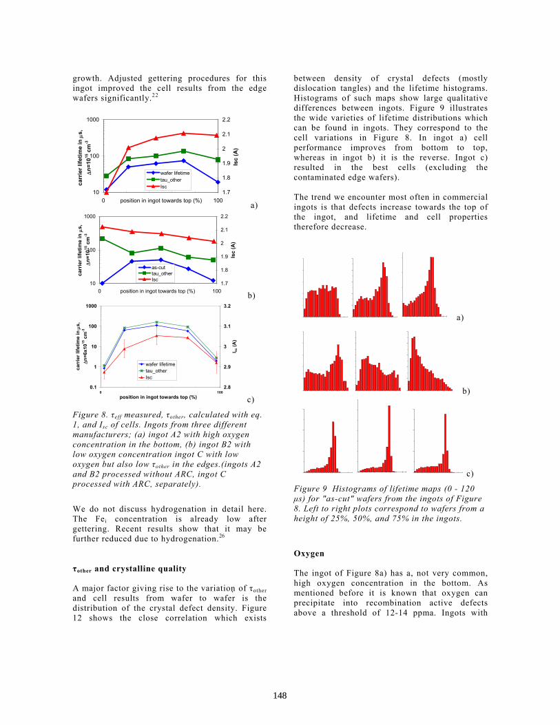
growth. Adjusted gettering procedures for this ingot improved the cell results from the edge wafers significantly.22
10
100
1000
0 100position in ingot towards top (%)
carr
ier l
ifetim
e in
µs,
∆
n=10
15 c
m-3
1.7
1.8
1.9
2
2.1
2.2
Isc
(A)
wafer lifetimetau_otherIsc
a)
10
100
1000
0 100position in ingot towards top (%)
carr
ier l
ifetim
e in
µs,
∆n=
1015
cm
-3
1.7
1.8
1.9
2
2.1
2.2
Isc
(A)
as-cuttau_otherIsc
b)
0.1
1
10
100
1000
0 100position in ingot towards top (%)
carr
ier l
ifetim
e in
µs,
∆
n=6x
1015
cm
-3
2.8
2.9
3
3.1
3.2
I sc (A
)
wafer lifetimetau_otherIsc
c)
Figure 8. τeff measured, τother, calculated with eq. 1, and Isc of cells. Ingots from three different manufacturers; (a) ingot A2 with high oxygen concentration in the bottom, (b) ingot B2 with low oxygen concentration ingot C with low oxygen but also low τother in the edges.(ingots A2 and B2 processed without ARC, ingot C processed with ARC, separately).
We do not discuss hydrogenation in detail here. The Fei concentration is already low after gettering. Recent results show that it may be further reduced due to hydrogenation.26 τother and crystalline quality A major factor giving rise to the variation of τother and cell results from wafer to wafer is the distribution of the crystal defect density. Figure 12 shows the close correlation which exists
between density of crystal defects (mostly dislocation tangles) and the lifetime histograms. Histograms of such maps show large qualitative differences between ingots. Figure 9 illustrates the wide varieties of lifetime distributions which can be found in ingots. They correspond to the cell variations in Figure 8. In ingot a) cell performance improves from bottom to top, whereas in ingot b) it is the reverse. Ingot c) resulted in the best cells (excluding the contaminated edge wafers). The trend we encounter most often in commercial ingots is that defects increase towards the top of the ingot, and lifetime and cell properties therefore decrease.
a)
b)
c)
Figure 9 Histograms of lifetime maps (0 - 120 µs) for "as-cut" wafers from the ingots of Figure 8. Left to right plots correspond to wafers from a height of 25%, 50%, and 75% in the ingots.
Oxygen The ingot of Figure 8a) has a, not very common, high oxygen concentration in the bottom. As mentioned before it is known that oxygen can precipitate into recombination active defects above a threshold of 12-14 ppma. Ingots with
148
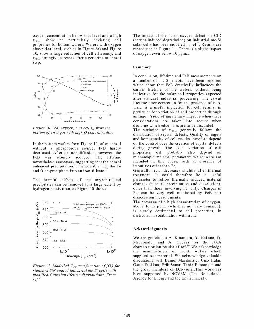
oxygen concentration below that level and a high τother show no particularly deviating cell properties for bottom wafers. Wafers with oxygen above that level, such as in Figure 8a) and Figure 10, show a large reduction of cell efficiency, and τother strongly decreases after a gettering or anneal step.
75
80
85
90
95
100
0 20 40 60 80 100 120position in ingot (mm)
I sc (%
)
0
5
10
15
20
FeB
in 1
011 c
m-3
, or
O in
ppm
a
SiNx ARC bulk-passivateduncoatedFeBFTIR-Oxygen
Figure 10 FeB, oxygen, and cell Isc from the bottom of an ingot with high O concentration.
In the bottom wafers from Figure 10, after anneal without a phosphorous source, FeB hardly decreased. After emitter diffusion, however, the FeB was strongly reduced. The lifetime nevertheless decreased, suggesting that the anneal enhanced precipitation. It is possible that the Fe and O co-precipitate into an iron silicate.27 The harmful effects of the oxygen-related precipitates can be removed to a large extent by hydrogen passivation, as Figure 10 shows.
1x10¹⁷ 1x1018560
570
580
590
600
610
620
Ope
n ci
rcui
t vol
tage
VO
C (m
V)
Average [Oi ] (cm-3)
initial area-averaged τ = 1000µs(equiv. to J0B-averaged τ = 115µs)
10µs (4.4µs)
30µs (12µs)
3µs (1.4µs)
100µs (32µs)
Figure 11. Modelled VOC as a function of [Oi] for standard SiN coated industrial mc-Si cells with modified-Gaussian lifetime distributions. From ref.7
The impact of the boron-oxygen defect, or CID (carrier-induced degradation) on industrial mc-Si solar cells has been modeled in ref.7. Results are reproduced in Figure 11. There is a slight impact of oxygen even below 10 ppma. Summary In conclusion, lifetime and FeB measurements on a number of mc-Si ingots have been reported which show that FeB drastically influences the carrier lifetime of the wafers, without being indicative for the solar cell properties expected after standard industrial processing. The as-cut lifetime after correction for the presence of FeB, τother, is a useful indication for cell results, in particular for variation of cell properties through an ingot. Yield of ingots may improve when these considerations are taken into acount when deciding which edge parts are to be discarded. The variation of τother generally follows the distribution of crystal defects. Quality of ingots and homogeneity of cell results therefore depend on the control over the creation of crystal defects during growth. The exact variation of cell properties will probably also depend on microscopic material parameters which were not included in this paper, such as presence of impurities other than Fei. Generally, τother decreases slightly after thermal treatment. It could therefore be a useful parameter to follow thermally induced material changes (such as precipitation and dissolution), other than those involving Fei only. Changes in Fei can be very well monitored by FeB pair dissociation measurements. The presence of a high concentration of oxygen, above 10-15 ppma (which is not very common), is clearly detrimental to cell properties, in particular in combination with iron. Acknowledgments We are grateful to A. Kinomura, Y. Nakano, D. Macdonald, and A. Cuevas for the NAA characterisation results of ref.19 We acknowledge the manufacturers of mc-Si wafers which supplied test material. We acknowledge valuable discussions with Daniel Macdonald, Giso Hahn, Gaute Stokkan, Erik Sauar, Tonio Buonassisi and the group members of ECN-solar.This work has been supported by NOVEM (The Netherlands Agency for Energy and the Environment).
149

0 10 20 30 40 0
10
20
30
40
0 10 20 30 400
10
20
30
40
0 10 20 30 40 0
10
20
30
40
Figure 12. Photographs after defect etch and corresponding MFCA lifetime maps of the three samples of Figure 8-b and Figure 9-b. X and Y dimensions are in mm. The MFCA grey scale is 0-130 µs (linear).
References 1 L.J. Geerligs, 12th NREL workshop on crystalline Si solar cells and materials, p. 288 (2002). 2 L.J. Geerligs, 3rd WCPEC, Osaka, p. 1044 (2003). 3 The calibration constant used for conversion of absorbance to concentration was the ASTM-1995 standard: 6.28 ppma-cm for oxygen (at ~1107 cm-1). The effective thicknesses of the floatzone reference wafer and the test wafers were matched using the Si phonon bands similar to the discussion in K. Krishnan et al., Characterization of Semiconductor Silicon using FTIR, in: practical Fourier Transform Infrared Spectroscopy, eds. J.R. Ferraro, K. Krishnan (Academic Press, 1990) p. 313. 4 methodology as in A. Schönecker et al., J. Appl. Phys. 79, 1497 (1996). 5 J.W. Mayer and S.S. Lau, Electronic Materials Science (Macmillan, 1988), p. 176. The rate of precipitate nucleation is a high power of the oxygen concentration, see Handbook of Semiconductor silicon technology, eds. O’Mara, Herring, and Hunt (Noyes publications, 1990). A threshold of around 14 ppma for the detrimental effects of oxygen was reported by. S. Martinuzzi et al., 13th EC-PVSEC, p. 1382 (1995). 6 J. Schmidt et al, 26th IEEE PVSC, Anaheim (1997); K. Bothe et al, 3rd WCPEC, Osaka, p. 1077 (2003); S. Rein et al, 3rd WCPEC, Osaka, p. 1048; p. 1057 (2003).; H. Nagel et al, 14th EC-PVSEC, 762-765 (1997); M. Dhamrin et al, 29th IEEE PVSC, New Orleans, 2002. 7 D. Macdonald et al., 13th NREL workshop on crystalline Si solar cells and materials, p. 182 (2003), focuses on evaluation of the effect in mc-Si. 8 K. Graff and H. Pieper, J. Electrochem. Soc. 128, 669 (1981); L.J. Geerligs and Daniel Macdonald, Dynamics of light-induced FeB pair dissociation in crystalline silicon, submitted to Appl.Phys.Lett. 9 L.C. Kimerling and J.L. Benton, Physica 116B, 297 (1983); L.C. Kimerling, Proc. of the MRS Annual Meeting, 1980, Boston, MA (North-Holland), p. 85. 10 G. Zoth and W. Bergholz, J. Appl. Phys. 67, 6764 (1990). 11 D. Macdonald, A. Cuevas, J. Wong-Leung, J. Appl. Phys. 89, 7932 (2001). 12 A.A. Istratov, H. Hieslmair, and E.R. Weber, Appl. Phys. A: Mater.Sci.Process. 69, 13 (1999). 13 D.H. Macdonald, L.J. Geerligs, and A. Azzizi, J. Appl. Phys. 95, 1021 (2004). 14 D. Macdonald and L.J. Geerligs, to be published.
150

15 L.J. Geerligs et al., Proceedings of the 12th workshop on crystalline silicon solar cell materials and processes, (NREL, 2003) p. 216. 16 M. Acciarri et al., 13th EC-PVSEC, 1336 (1995). 17 M. Rinio, C. Ballif, T. Buonassisi, and D. Borchert, Defects in the deteriorated border layer of block-cast multicrystalline silicon ingots. To be published in the proceedings of the 19th EC-PVSEC, June 2004, Paris. 18 D. Macdonald, A. Cuevas, A. Kinomura, and Y. Nakano, 29th IEEE PVSC, New Orleans, (2002); A. A. Istratov et al,. J. Appl. Phys. 94, (2003), 6552. 19 D. Macdonald, A. Kinomura, Y. Nakano, L. J. Geerligs and A. Cuevas, Interstitial and Precipitated Iron Content of a Photovoltaic-Grade Cast Multicrystalline Silicon Ingot, submitted to 4th International Symposium on Advanced Science and Technology of Silicon Materials, Nov. 22-26, 2004, Kona, Hawaii; and to be published. 20 see e.g. Schei, Tuset, and Tveit: High Silicon Alloys (TAPIR Forlag, Trondheim, 1998). 21 T. Buonassisi, private communiation; A. A. Istratov, W. Huber, and E. R. Weber, Experimental evidence for the presence of segregation and relaxation gettering of iron in polysilicon layers, submitted to Appl. Phys. Lett.; T. Buonassisi et al., Synchrotron-based investigations of the nature and impact of iron contamination in multicrystalline silicon solar cell materials, submitted to J. Appl. Phys. 22 P. Manshanden et al., to be published. 23 C. Ballif et al., 17th European PVSEC, 1818 (2001). 24 L. Caballero et al., 3rd WCPEC, Osaka, p. 1013 (2003). 25 for relation of lifetime distribution to cell results, see, e.g., W. Warta et al., 2nd World Conference on PVSEC, 1650 (1998); B.L. Sopori, Mater. Sci. Forum 258-263, 527 (1997); J. Isenberg et al., 29th IEEE PVSC, (2002), R.A Sinton, 3rd WCPEC, Osaka, p. 1028 (2003); S. Riepe et al., Increased wafer yield for solar cells in top and bottom regions of cast multicrystalline silicon, 18th European PVSEC (Paris, 2004); and references therein. 26 A. Azzizi, et al., Hydrogen passivation of iron in crystalline silicon, to be published in the proceedings of the 18th EC-PVSEC (Paris, 2004). 27 S. McHugo et al., Physica B 273-274, 371 (1999).
151

EVALUATING SILICON BLOCKS AND INGOTS WITH QUASI-STEADY-STATE AND TRANSIENT LIFETIME MEASUREMENTS
R. A. Sinton
Sinton Consulting, Inc., Boulder CO USA. www.sintonconsulting.com
ABSTRACT: This paper reviews recent work on the problem of measuring bulk lifetime on industrial blocks and boules of silicon for use in solar cell manufacture. The Quasi-Steady-State Photoconductance technique, previously common in R&D wafer measurements, has been applied to measure the lifetime in multicrystalline blocks and solar CZ boules. This paper reviews progress towards obtaining an absolute calibration for QSSPC block measurements in order to enable device physics studies on multicrystalline blocks as they exist in the production line. Detailed characterization of blocks of silicon prior to sawing provides data on silicon ingot growth and improves decisions on wafering. Results are presented for the determination of Fe concentration and trapping based on lifetime measurements. The combination of lifetime, Fe, and trapping data will provide much better prediction of wafer yield than lifetime data alone. In long lifetime CZ or FZ boules, transient photoconductance measurements can be performed with the same type of instrument. Lifetime measurements have also been optimized for these cases. While transient lifetime measurements require fewer assumptions and are less dependent upon correction for surface recombination for accurate lifetime determination, the use of the transient technique presents difficulties in reporting calibrated minority-carrier densities.
1 INTRODUCTION Most previous work using the QSSPC method has determined the area-averaged lifetime over an area of approximately 4 cm diameter on wafers. Recently, this has been extended to measure the lifetime in blocks, boules or ingots as well[3]. In this paper, we will review spatially-resolved block measurements achieved by limiting the light to a well defined line as shown in Fig. 1. Using this line, an average lifetime is measured over the height of the line (30 mm), but a resolution of 2 mm is achieved in the width direction. This can be used for lines scans of multicrystalline blocks, with good resolution in the scan (growth) direction. Once the different geometry of blocks compared to wafers is taken into account, the standard QSSPC data analysis[1] can be performed on the resulting data giving the lifetime as a function of injection level. QSSPC measurements on wafers have been used to investigate trapping and Fe concentrations as well as for the measurement of lifetime[2]. This paper describes similar measurements taken directly on production silicon blocks. Different optimizations are required for the measurements on CZ and FZ boules. In particular, the use of transient photoconductance measurements is discussed for the case of measurements on FZ boules. 2 CALIBRATION OF THE QSSPC METHOD FOR USE IN CZ OR MULTICRYSTALLINE BLOCKS. The difficulty of calibrating the instrument is illustrated by Fig. 2. When doing any recombination
study, it is vital to know the minority-carrier density where the lifetime is measured. The photoconductance instrument measures the total photoconductance[1]. Fig. 2 shows the minority carrier density in the surface 2 mm that results from steady-state illumination of a 1-ohm-cm p-type block of silicon. The bulk lifetime is 2µs, the surface recombination velocity is 2x105 cm/s and the absorption depth of the light is 20 µm. We hypothesize that an appropriate choice for the carrier density that represents this type of distribution is given by the weighted average of the carrier density, where the weighting function is the carrier density. This gives the average carrier density seen by the average minority carrier. The resulting effective carrier density and depth is shown in Fig. 2. This is the carrier density that will be reported for a measured lifetime. In addition, since the electron mobility is dependent upon carrier density, this calculated carrier density is also used in the conversion of photoconductance to minority-carrier density.
Scan 1
Scan 3
Scan 2
Bottom Top
Figure 1: The photoconductance is determined by a 3 by 30 mm illumination pattern through the sensor. This pattern is scanned across the block, giving high resolution in the growth direction. For this work, IR-pass filters were used in conjunction with a xenon flashlamp[3] rather than a monochromatic
152

source as shown in Fig. 2. As a result, the functions illustrated by Fig. 2 were evaluated using PC1D to determine the minority-carrier density profiles that result from the photon distribution of the light from the flash and filter[6].
0.0E+00
5.0E+13
1.0E+14
1.5E+14
2.0E+14
2.5E+14
3.0E+14
3.5E+14
4.0E+14
0 0.05 0.1 0.15 0.2
width (cm)
Elec
tron
Con
cent
ratio
n (c
m-3
)
Weighted electron density
Mean electron density
Figure 2: An illustration of the electron carrier density profile in the top 2mm of a silicon block, and the weighted carrier density used in the analysis and reported for each measurement. A second challenge in measuring blocks is that the surface is not passivated. The resulting high-surface re-combination will result in a measured lifetime that is much lower than the bulk lifetime. In this work, PC1D was used to evaluate the transfer function from the measured to bulk lifetime for the lifetime range and photon distribution in this experiment. This is shown in Fig. 3. The work will be detailed in a future publication[6]. 3 MEASUREMENTS OF LIFETIME, TRAPPING, AND IRON CONCENTRATIONS
Unfortunately, it has been shown that the lifetime of as-grown multi-crystalline silicon is often only loosely correlated with the solar cell efficiency that will result. The high temperature processing and resulting gettering both fundamentally change the material during processing. However, measurements on wafers have indicated that if the Fe concentration is measured and the effect of it is removed from the lifetime data of as-grown material, then the solar cell efficiency can be predicted with much better accuracy[2]. The method is to light-soak the wafer and determine the dissolved Fe concentration by noting the change in lifetime at a spe-cific calibrated minority-carrier density[2,4].
The lifetime profile in a line scan along the length of a block is shown in Fig. 4. The lower curve was taken before light soaking, and the upper curve directly after light soaking for two minutes. The light soaking was done using 400W of halogen light incident on a 3-cm-wide line down the length of the block. Over the course of a few hours, the lifetime returned to the initial value. This is another characteristic of Fe in Boron-doped silicon. Both before and after light soaking, this block shows very long lifetime. For long-lifetime homogeneous material, as is evident from the QSSPC results in Figure 4, transient photoconductance measurements can be performed with the same instrument to validate the QSSPC analysis methodology[3]. The resulting lifetime for the peak lifetime region of Figure 4 was 306 µs, as measured from the transient photoconductance decay.
Simulation of measured lifetime with PC1D
1
10
100
1000
0.1 1.0 10.0 100.0 1000.0Measured lifetime (µs)
Bul
k lif
etim
e (µ
s)
RG1000 IR
RG850 IR
BG-38
Figure 3: The transfer function from measured lifetime to bulk lifetime as evaluated using PC1D[9] for 1 Ohm-cm p-type silicon and the photon distribution in the filtered light source[3]. In this paper, data from the RG-850 filter is presented.
0
50
100
150
200
250
300
0 5 10 15 20 25
Cm from bottom (as grown)
Life
time
( µs)
Figure 4: A linescan along the length of a multicrystalline block directly before and after light soaking.
153
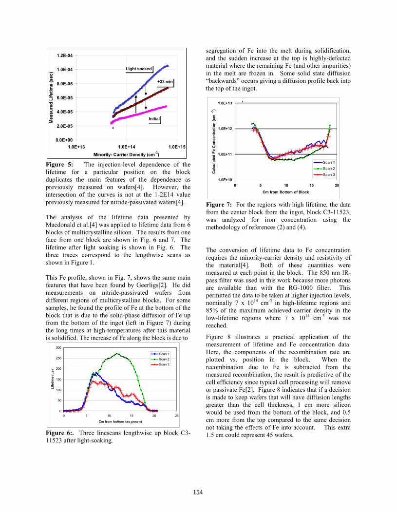
0.0E+00
2.0E-05
4.0E-05
6.0E-05
8.0E-05
1.0E-04
1.2E-04
1.0E+13 1.0E+14 1.0E+15Minority- Carrier Density (cm-3)
Mea
sure
d Li
fetim
e (s
ec)
Initial
Light soaked
+33 min
Figure 5: The injection-level dependence of the lifetime for a particular position on the block duplicates the main features of the dependence as previously measured on wafers[4]. However, the intersection of the curves is not at the 1-2E14 value previously measured for nitride-passivated wafers[4]. The analysis of the lifetime data presented by Macdonald et al.[4] was applied to lifetime data from 6 blocks of multicrystalline silicon. The results from one face from one block are shown in Fig. 6 and 7. The lifetime after light soaking is shown in Fig. 6. The three traces correspond to the lengthwise scans as shown in Figure 1. This Fe profile, shown in Fig. 7, shows the same main features that have been found by Geerligs[2]. He did measurements on nitride-passivated wafers from different regions of multicrystalline blocks. For some samples, he found the profile of Fe at the bottom of the block that is due to the solid-phase diffusion of Fe up from the bottom of the ingot (left in Figure 7) during the long times at high-temperatures after this material is solidified. The increase of Fe along the block is due to
0
50
100
150
200
250
300
0 5 10 15 20 25
Cm from bottom (as grown)
Life
time
( µs)
Scan 1Scan 2Scan 3
Figure 6:. Three linescans lengthwise up block C3-11523 after light-soaking.
segregation of Fe into the melt during solidification, and the sudden increase at the top is highly-defected material where the remaining Fe (and other impurities) in the melt are frozen in. Some solid state diffusion “backwards” occurs giving a diffusion profile back into the top of the ingot.
1.0E+10
1.0E+11
1.0E+12
1.0E+13
0 5 10 15 20
Cm from Bottom of Block
Cal
cula
ted
Fe C
once
ntra
tion
(cm
-3)
Scan 1Scan 2Scan 3
Figure 7: For the regions with high lifetime, the data from the center block from the ingot, block C3-11523, was analyzed for iron concentration using the methodology of references (2) and (4).
The conversion of lifetime data to Fe concentration requires the minority-carrier density and resistivity of the material[4]. Both of these quantities were measured at each point in the block. The 850 nm IR-pass filter was used in this work because more photons are available than with the RG-1000 filter. This permitted the data to be taken at higher injection levels, nominally 7 x 1014 cm-3 in high-lifetime regions and 85% of the maximum achieved carrier density in the low-lifetime regions where 7 x 1014 cm-3 was not reached.
Figure 8 illustrates a practical application of the measurement of lifetime and Fe concentration data. Here, the components of the recombination rate are plotted vs. position in the block. When the recombination due to Fe is subtracted from the measured recombination, the result is predictive of the cell efficiency since typical cell processing will remove or passivate Fe[2]. Figure 8 indicates that if a decision is made to keep wafers that will have diffusion lengths greater than the cell thickness, 1 cm more silicon would be used from the bottom of the block, and 0.5 cm more from the top compared to the same decision not taking the effects of Fe into account. This extra 1.5 cm could represent 45 wafers.
154

0.001
0.01
0.1
0 5 10 15 20Cm from bottom
Rec
ombi
natio
n R
ate
( µs-1
)
Measured
Iron (Fe)
Unidentif ied
L=300 µm
Figure 8. The recombination due to iron calculated for the concentrations shown in Fig. 7. When this is subtracted from the measured data, the result, “other” recombination, is predictive of cell performance[2]. The recombination rate where diffusion length equals cell thickness is shown for reference.
0
20
40
60
80
100
120
0 5 10 15 20 25
Cm from bottom
Life
time
( µs)
Scan 1Scan 2Scan 3
Figure 9. The lifetime scans for a corner block from the ingot, E1-11523, with an interesting lower-lifetime feature at 13 cm.
Figure 9 shows lifetime scans from one face of a corner block from an ingot. This lifetime scan shows an interesting dip in lifetime, for all three scans, at about 13-14 cm. The calculated Fe concentration from this block, Fig. 10, does not show any peak in the Fe concentration at this point, indicating that dissolved Fe is not the cause of this low-lifetime region. Another parameter that was measured in these line scans was the “trapping” as defined in references [7] and [8]. This trapping has been shown to correlate with poor crystalline quality, including dislocation densities [8]. In Fig. 11, there is a strong peak in the trapping at the point where the lifetime dips. For comparison, the trapping for the center block C-11523 is shown in Fig. 12. For C3-11523, the overall trapping levels are much lower than in the corner block E1-11523. A peak in the trapping at 17 cm in one of the scans does correlate with a drop in lifetime at that same spot in the lifetime scan. Again, this lifetime dip correlates better with this trapping than with the Fe concentration.
1.0E+10
1.0E+11
1.0E+12
1.0E+13
0 5 10 15 20
Cm from Bottom of Block
Cal
cula
ted
Fe C
once
ntra
tion
(cm
-3)
Scan 1Scan 2Scan 3
Figure 10. The calculated Fe concentrations for the corner block shown in Fig. 9. The low-lifetime feature at 13 cm is apparently not correlated with high dissolved Fe concentration. In contrast, the low lifetime of one edge, labeled “scan 1” is directly correlated with the calculated Fe concentration.
0
5E+13
1E+14
1.5E+14
2E+14
2.5E+14
3E+14
3.5E+14
4E+14
4.5E+14
0 5 10 15 20 25
Cm from bottom
"Tra
ps"
(A.U
. )Scan 1Scan 2Scan 3
Figure 11. Trapping, as defined in Ref [7] and [8] vs. position from the bottom of the block shown in Fig. 9 and Fig. 10. The strong dip in lifetime at 13-14 cm correlates with this trapping parameter. Measurements such as those shown here, done on industrial blocks, have the potential to make a large impact on solar cell yields and efficiency. For example, it has been shown that the lower-lifetime regions at the top and the bottom of ingots respond dramatically differently to gettering processes, indicating that there is a different optimal process for wafers with different defects[10]. If measurements at the block level could identify the different types of material, then they could be sorted so that the optimum process could be used for different “types” of wafer. This could give very significant improvements in efficiency and yield with little or no effect on costs. This would be in contrast to existing lines that have processes that have a window wide enough to work moderately well for every wafer processed from a block. By definition, if different wafers respond to different processes, then a single process for all wafers
155

results in lower that optimal efficiencies for most wafers. We look forward to the studies that would be necessary to prove out these possible gains. 4 TRANSIENT LIFETIME MEASUREMENTS ON
LONG LIFETIME FZ AND CZ MATERIAL
For long lifetime material, transient phococonductance measurements seem to provide the best measurements. When the lifetime is long, the photoconductance decay can be measured after the minority carriers near the surface have largely decayed away, leaving primarily bulk recombination to determine the lifetime. By using this approach, the numerical transfer function between measured and bulk lifetime is largely unnecessary, as is the calculation and calibration of the photogeneration in the silicon. This transient technique has long been applied for lightly doped material, as specified by ASTM. However, the ASTM method is difficult to apply to doped material. Other techniques, such as one based upon a probed conductance measurement at the surface with a laser photoexcitation have been developed for doped materials[11]. We have developed contactless transient measurement methods that can be used with similar Sinton Consulting lifetime test instruments as those discussed for the QSSPC measurements in this paper.
Figure 12 shows how the electron density profile evolves from the steady state case after illumination is terminated, based on PC1D[12] simulations While in the steady state with illumination, there is a high minority carrier density in proximity to the surface. This is why the large correction to the measured lifetime as shown in Fig. 3 is required for steady state measurements. However, after the light is extinguished, the minority carrier density near the surface quickly falls, and becomes limited by the rate at which the minority carriers can diffuse to the surface. With increasing time, the photoconductance decay time will approach the bulk lifetime for these minority carriers.
This evolution is shown in Fig. 13. For electrons in p-type material, the measured lifetime is significantly lower than the bulk lifetime initially after the light is terminated. This is shown as the lifetime at the peak signal in Fig. 13. After several lifetimes have passed, the measured lifetime approaches the actual bulk lifetime. Small effects due to the surface recombination remain for varying amounts of time. For long-lifetime material, such as the 1 ms case shown in Fig. 13, the measured lifetime will always give a lower bound on the actual bulk lifetime, as even after
the signal has dropped by 2 orders of magnitude, the measured lifetime is estimated to be only 70% of the actual bulk lifetime. This simulation was based on the integral of the modelled photoconductance decay in the top 3 mm of the silicon block, corresponding roughly to the depth of silicon that is sensed by the lifetime test instrument.
1.0E+12
1.0E+13
1.0E+14
1.0E+15
1.0E+16
0 0.005 0.01 0.015 0.02 0.025
Distance into Si (m)C
arrie
r Den
sity
Carrier Density illuminated
After 0.5 ms
After1.0 ms
After 2.0 ms
After 4.0 ms
3 mm
Figure 12. The evolution of electron carrier density from the steady-state condition after illumination is terminated. Data for the lifetime measured in this way on 1.6 ohm-cm p-type silicon boule is shown in Fig. 14. The interpretation of this data is complex for several reasons. First, the lifetime at higher carrier density is low due to the surface recombination. The lifetime at low carrier density is injection-level dependent, as is typical for the bulk lifetime in p-type silicon. Since these trends are opposing, there is a maximum measured lifetime, shown as about 3 x 1014 cm-3 injection level. Since this data at 3 x 10¹⁴ is only 1 order of magnitude down from the peak intensity, this is clearly a lower bound on the actual bulk lifetime, probably underestimating the actual bulk lifetime by up to 40%. Lastly, because of the complexity of the evolution of the carrier density profile with time, an absolute calibration of the injection level has not been done on the data shown in Fig. 14. Instead, a carrier density is reported based on the approximation of the sensed photoconductance electrons are in the first 2 mm from the surface, and this resulting carrier density is the one determining the lifetime.
156

Simulation P-type Si
0.000001
0.00001
0.0001
0.001
0.001 0.01 0.1 1 10
Fraction of peak carrier density
Mea
sure
d Li
fetim
e (s
ec)
Surface passivated
Surface unpassivated
Time after fllash
Figure 13. When the light is extinguished, the highest carrier density is recorded as shown in Fig. 12. As the electrons near the surface decay away (right to left in this figure), the measured lifetime approaches the actual bulk lifetime. The initial lifetime will depend on the wavelength of light used for illumination. 10-5, 10-
4, and 10-3 second lifetime cases are shown.
Figure 14. The lifetime reported using the method described in this work. The lifetime at high injections levels is measured low due to surface recombination. In the future, more work is required to improve this calibration of the injection level to be reported from transient measurements done with this technique. 4. CONCLUSIONS
This paper presents a methodology for obtaining calibrated quasi-steady-state photoconductance measurements on Si blocks. This was demonstrated by measuring lifetime, Fe, and trapping on multicrystalline blocks. The results show similar trends to previous studies done on wafers cut from various positions in silicon blocks and surface passivated with a nitride deposition[2]. In regions where Fe is known to diffuse into the crystal from the crucible or is frozen into the crystal at the top of the ingot, high-levels of Fe were
Figure 15. The photoconductance and light intensity signal corresponding to the data in Fig. 14.A long pulse is used to pump the sample with electrons nearly into the steady state, then the light pulse is terminated and the transient decay is observed and analyzed.
observed resulting in low lifetime. Some other low-lifetime regions were present that did not correlate with dissolved Fe. In this initial study, these regions appear to correlate with trapping. The distinction is important, as poor lifetime due to Fe contamination can recover due to gettering and hydrogen passivation in the cell process. Poor lifetime due to poor crystalline quality is likely to result in solar cells with poor efficiency[2]. The results in this paper support previous studies that indicate that better decisions can be made on which sections of a block to saw into wafers for processing and which sections to recycle [2]. This work demonstrates a method for obtaining this data on industrial blocks in the production process. This could provide immediate feedback to crystal growth in both research and industrial settings, as well as optimize the yields of wafered silicon into efficient solar cells. For long-lifetime boules of FZ or CZ material, measurements have been optimized using the transient photoconductance decay technique with the same instrument. Transient measurement on blocks require fewer assumptions than QSSPC measurements to obtain relatively accurate lifetime results despite unpassivated surfaces. However, more work is required before the minority-carrier injection level that is reported is fully calibrated.
Illumination at Reference Cell and PC Signal
0.10
1.00
10.00
100.00
1000.000.0E+00 2.0E-03 4.0E-03 6.0E-03 8.0E-03 1.0E-02
Time (s)
Illum
inat
ion
Inte
nsity
(Sun
s)
0 .000
0.001
0.010
0.100
1.000
10.000
Phot
o-C
ondu
ctan
ce S
igna
l (V)
Intensity (Suns)
PC signal
First point analyzed
Minority-Carrier Lifetime vs. Carrier Density
0.000
0.001
0.002
0.003
1.0E+13 1.0E+14 1.0E+15 1.0E+16
Estimated Minority- Carrier Density (cm-3)
Mea
sure
d Li
fetim
e (s
ec)
Minority-Carrier Density
Maximum Lifetime
Apparent Carrier Density
Tau = 1403.2 µs at 4.8E+14 cm-3
157

ACKNOWLEDGEMENTS: The author would like to thank the following co-workers for collaborations and discussions of various parts of this work, including Tanaya Mankad, Stuart Bowden, Nicolas Enjalbert of Photowatt, Dan Macdonald of ANU and Bart Geerligs of ECN. This work was partially supported by U.S. D.O.E. subcontract ZDO-2-30628-08. REFERENCES [1] R. Sinton and A. Cuevas, APL 69, 2510, (1996). [2] L. J. Geerligs, Proc. 3rd World Conference on PVSEC, Osaka, 2003. [3] R. A. Sinton, Tanaya Mankad, Stuart Bowden, and Nicolas Enjalbert, Proc. EPSEC, Paris 2004. [4] D. H. Macdonald, L. J. Geerligs and A. Azzizi, JAP 95(3) Feb.1 2004, pp.1021-1028. [5] R. A. Sinton and T. Mankad, 13th NREL Workshop on Crystalline Materials and Processes, Aug. 2003. [6] S. Bowden and R. A. Sinton, to be published. [7] D. Macdonald, R. A. Sinton, and A. Cuevas, JAP V89 (5) 2001, pp. 2772-2778. [8] D. Macdonald and A. Cuevas, APL 74 (12) 22 March 1999, pp. 1710-1712. [9] P. A. Basore and D. A. Clugston, 26th PVSC Anaheim, 1977 pg. 207. [10] S. Riepe, M Ghosh, A. Muller, H. Lautenschlager, D. Grote, W. Warta, and R. Schindler, Proc. EPSEC, Paris 2004. [11] T. F. Ciszek, T. H. Wang, M. Landry, A. Matthaus, G. B. Mihalik, Presented at the Electrochemical Society Joint Meeting, Oct. 1999. [12] P. A. Basore and D. A. Clugston, 26th PVSC Anaheim, 1977 pg. 207.
158

Advanced In-Line Quality Control of Crystalline Silicon Wafers and Solar Cells
Peter Fath, University of Konstanz
Manuscript not available at time of printing.
159

Wafer characterisation and mechanical properties Author: Dr. techn. Erik Sauar, Renewable Energy Corporation / ScanWafer, PO Box 280, 1381 Høvik, Norway. E-mail: [email protected] Extended Abstract Thinner wafers, larger wafers and automated production are three main routes to substantially lower the cost of photovoltaic modules made from crystalline silicon. All these three possibilities are currently being pursued by the PV industry, and they all have one requirement in common; mechanical wafer strength. Such strength is also increasingly being required in order to achieve lead-free soldering of the cells. The wafers made at ScanWafer are a result of a multi-step production process. We have found mechanical wafer strength to be affected by almost all our production steps: the crystallisation process, the ingot cutting process, the wafer cutting process and by the mechanical handling and quality control operations. Not surprisingly, we have also found that thinner and larger wafers are more fragile than thick and small wafers. In order to optimise the production process efficiently and secure that only strong wafers proceed to cell manufacturing, wafer characterisation and data gathering is of high importance. Hence, an increasing set of characterisation tools are applied on a regular and statistical sampling basis. Such characterisation tools include minority carrier life time on uncut blocks, roughness measurement of block surface, wafer thickness measurements, saw mark detection, life-time of wafers and wafer strength measurements. In the presentation some of our findings and characterisation tools will be presented with a special emphasis on identifying key factors that affect the strength of our wafers.
160

Distribution and Chemical State of Cu-rich Clusters in Silicon
T. Buonassisi1,2, M. A. Marcus3, A. A. Istratov1,2, M. Heuer4, T. F. Ciszek5, B. Lai6, Z. Cai6, and E. R. Weber2,1
1. Materials Sciences Division, Lawrence Berkeley National Laboratory, Berkeley, CA 2. Department of Materials Science, University of California at Berkeley, Berkeley, CA 3. Advanced Light Source, Lawrence Berkeley National Laboratory, Berkeley, CA 4. Institute of Mineralogy, Crystallography, and Materials Science, University of Leipzig, Leipzig, Germany 5. National Renewable Energy Laboratory, Golden, CO; present address: Siliconsultant, Evergreen, CO 6. Advanced Photon Source, Argonne National Laboratory, Argonne, IL Copper is a ubiquitous contaminant in silicon-based device technology that can be easily introduced into the bulk of silicon wafers. According to the existing data on solubility and diffusivity of Cu in Si [1-3], at only 425°C the equilibrium solubility of Cu in Si is as high as 1013 cm-3, and the diffusivity is such that Cu can traverse 220 µm of single crystalline p-type silicon in under 10 seconds ( λ ≅ 4Dt ). According to the current understanding of the electrical properties and defect interactions of copper in silicon [4, 5], inter-stitial copper is a shallow donor with relatively benign electrical activity. On the other hand, copper-rich precipitates are known to severely reduce the minority carrier diffusion length by forming bands of states within the silicon bandgap, thereby providing very effective pathways for recombination [6-8]. It is thus of interest to investigate the distribution and chemical state of copper-rich clusters in a variety of silicon mate-rials, including model defect structures and mc-Si solar cell material. For this purpose, we employed a vari-ety of synchrotron-based analytical techniques: X-ray fluorescence microscopy (µ-XRF), X-ray absorption microspectroscopy (µ-XAS), and X-ray beam induced current (XBIC). Four types of materials were utilized in this study: Sample 1: Float zone silicon intentionally con-taminated with (3-4)×1016 Cu/cm-3 during crystal growth. Float zone crystals were grown at the National Renewable Energy Laboratory (see Ref. 9 for details). The particular crystal growth conditions lead to a high density of structural defects. With no intentional n- or p-type doping, the actual conductivity of the sample was n-type, as evidenced by the rectifying behavior of a thin Pd diode evaporated on the polished and chemically cleaned surface. In µ-XRF mapping, irregularly distributed Cu clusters are observed at structural defects (Fig. 1b). This irregular Cu decoration is expected for slow-cooled samples, wherein su-persaturated Cu can diffuse to preferred precipitation sites [10]. The observed Cu-rich clusters are strongly recombination-active, as revealed by XBIC (Fig. 1a). Five Cu-rich clusters in this sample were analyzed by µ-XAS. Sample 2: Misfit dislocation heterostructure, consisting of a 2 µm thick n-type Si0.98Ge0.02 middle layer between a 2.5 µm n-type silicon bottom buffer layer on a (001) silicon substrate and a 2.5 µm thick n-type silicon cap layer. At the two interfaces between the SiGe and Si layers, a network of 60° misfit disloca-tions forms parallel to the surface and propagates in the <110> directions, intersecting at 90° angles. Copper was intentionally diffused at 800°C. Samples were fabricated at North Carolina State University (U.S.A.) and copper-contaminated at King's College (U.K.); further details of sample preparation can be found in Ref. 11. In µ-XRF mapping, Cu-rich precipitates are observed along the misfit dislocations. From the Cu-Kα fluorescence map (Fig. 2), one can clearly see the copper contamination along the network of misfit dislocations parallel to the surface, which intersect at 90° angles in agreement with literature observations [12]. The recombination-activity of these precipitates has been well-established by electron beam induced current (EBIC) and XBIC measurements, and is reported elsewhere [11-13]. Two Cu-rich clusters were ana-lyzed by µ-XAS in this sample. Sample 3: Czochralski silicon containing approximately 1.8×106 cm-3 oxygen precipitates and ap-proximately 1.5×1015 cm-3 boron was chosen because of the high density of precipitation sites for metals and high precipitated oxygen concentration. The sample was intentionally contaminated with Cu and an-nealed at 1200°C in forming gas (N2 + 5%H2) ambient for 30 minutes. The anneal was terminated by an air cool. In µ-XRF mapping, approximately ~1.1×106 cm-3 copper clusters are observed (assuming a Cu-Kα attenuation length of 70 µm and an angle of 45° between the sample surface normal and the detector). Al-though each Cu-rich cluster covers many pixels in the µ-XRF map (each pixel = 7×7 µm2) to form a disk- or point-like shape, as evidenced in Fig. 3, the average signal strength within the precipitate is low, evidence for the distribution of Cu in the form of many smaller precipitates. Cu nanoprecipitates have been observed
161

in infrared transmission microscopy [14], TEM [15], and etching experiments [16] to form elliptical, plate-like, micron-sized colonies of along preferred crystallographic orientations. Interestingly, the elliptical Cu-rich microcolonies observed in µ-XRF also appear to be aligned to certain orientations within the crystal, as shown in Fig. 3. Although the spatial density of these colonies (~1.1×106 cm-3) corresponds well to the den-sity of oxygen precipitates (1×106 cm-3), the morphology of these Cu clusters appears not to be spherical, indicating that the Cu atoms in this sample preferred not to homogeneously coat the oxygen precipitates, but either used them or their punched out dislocation loops as nucleation sites for Cu microcolony formation. Three Cu-rich clusters were analyzed by µ-XAS in this sample. Sample 4: As-grown, cast mc-Si wafer extracted from near the bottom of the cast mc-Si ingot, where the interstitial oxygen concentration can be as high as 1018 cm-3. In µ-XRF mapping, Cu-rich clusters were located at a grain boundary in the material, together with similar amounts of Ni and less abundant Fe, although no intentional contamination was performed. The µ-XRF map in Fig. 4 shows the Cu distribution along a representative region of the grain boundary. Although the cluster sizes were smaller than the x-ray beam spot size of 200 nm, the number of Cu atoms per cluster was determined to fall within the range of (3±1.5)×107 by comparison with standard materials. Were all these Cu atoms contained within one large spherical Cu3Si particle, the diameters of these particles would be around 100±15 nm. However, it is also possible these Cu3Si molecules are distributed among a colony of nanoparticles as reported in TEM studies of intentionally-contaminated monocrystalline Si [15]. Seven Cu-rich clusters were analyzed by µ-XAS in this sample. Cu K-edge µ-XAS scans of the copper-rich clusters in all four samples yielded strikingly similar spectra to Cu3Si standard material (Fig. 5b, c). It is interesting to note that Fig. 5a reveals that the Cu K-edge absorption onset energy of Cu3Si matches that of the Cu2O standard, and not metallic Cu. The Cu K-edge absorption energy shift of Cu3Si relative to Cu metal is atypical for metal silicides. Iron metal and sili-cides, for example, have identical Fe K-edge x-ray absorption onset energies, unlike oxidized iron species that have K-edge onsets shifted to higher energies by amounts proportional to the Fe charge state [17]. For Cu, a quantified absorption edge shift is clearly not sufficient for determining a specific oxidation state; in-stead, one has to match the whole near-edge absorption spectrum with that of a standard. The abnormal behavior of Cu stems from the unique electronic properties of Cu in Si. Copper dis-solved in p-type silicon is well-known to diffuse predominantly as Cui
+.1 Recent ab initio Hartree-Fock cal-culations published by S. K. Estreicher [5] indicate that Cui
+ will not diffuse as a compact [Ar]3d104s0 sphere, but rather, it will promote some its electrons from the 3d to the 4sp orbitals to form weak covalent bonds with nearby silicon atoms. Similarly, copper atoms precipitated at certain internal voids are predicted to promote a small fraction of their electrons to 4sp orbitals for covalent overlap with neighboring silicon atoms [5]. Macroscopic studies on and models of the properties of copper silicides have also indicated a hybridization of the valence Cu and Si orbitals [18-21]. The increased delocalization of Cu valence elec-trons can qualitatively explain the Cu-K absorption edge shift to higher energies: as they are photo-excited out of the atom, Cu 1s core electrons experience a greater Coulombic attraction with the Cu nucleus due to reduced electron screening, and thus require higher x-ray energies for photoionization. The energy-shifted absorption edge of Cu3Si is thus concluded not to be indicative of copper oxide or silicate formation. In fact, it is unlikely that Cu forms an oxidized phase in Si, because of the strong binding energy between oxygen and silicon. In effect, Cu cannot “out-compete” silicon for the oxygen, and thus remains a silicide. This effect is confirmed by computer modeling of West et al. [22], wherein the local distortion around an interstitial oxygen atom may be sufficient to attract an interstitial copper ion, Cui
+, but no signifi-cant overlap of electronic orbitals (i.e. electronic binding) occurs between the Cui
+ and the Oi. Because of the relatively low binding energy of Cu to Cu3Si precipitates, clusters of this phase are easily dissolved during heat treatments. Experiments studying this effect are reported in “Aluminum Getter-ing and Dissolution of Cu3Si Preciptiates in Silicon” by Buonassisi et al. in these proceedings. To conclude, the chemical state and distribution of Cu-rich clusters were determined in four differ-ent silicon-based materials with varying contamination pathways and degrees of oxygen concentration, in-cluding as-grown multicrystalline silicon. In all four samples, Cu3Si was the only chemical state observed. Cu3Si clusters were observed at structural defects within all four materials; XBIC measurements revealed that the presence of Cu3Si corresponds to increased recombination activity. Oxidized Cu compounds are not likely to form in silicon. The +1 eV edge shift in the µ-XAS absorption spectrum of Cu3Si relative to Cu metal is believed to be an indication of a degree of covalent bonding between Cu atoms and their silicon neighbors.
162

Acknowledgements The fruitful interactions with Stefan K. Estreicher and his team are greatfully acknowledged. This study was supported by NREL subcontract AAT-2-31605-03. The operations of the Advanced Light Source at Lawrence Berkeley National Laboratory are supported by the Director, Office of Science, Office of Basic Energy Sciences, Materials Sciences Division, of the US Department of Energy under Contract No. DEAC03-76SF00098. Use of the Advanced Photon Source was supported by the US Department of Energy, Office of Science, Office of Basic Energy Sciences, under Contract No. W-31-109-ENG-38. References: [1] R. N. Hall, and J. H. Racette, Journal of Applied Physics 35, 379 (1964). [2] E. R. Weber, Appl. Phys. A: Solids Surf. 30, 1 (1983). [3] A. A. Istratov, C. Flink, H. Hieslmair, E. R. Weber, and T. Heiser, Phys. Rev. Lett. 81, 1243 (1998). [4] A. A. Istratov, and E. R. Weber, J. Electrochem. Soc. 149, G21 (2002). [5] S. K. Estreicher, Physical Review B 60, 5375 (1999). [6] J.-L. Maurice, and C. Colliex, Applied Physics Letters 55, 241 (1989). [7] A. Broniatowski, Philosophical Magazine B (Physics of Condensed Matter, Electronic, Optical and Magnetic
Properties) 66, 767 (1992). [8] A. A. Istratov, H. Hedemann, M. Seibt, O. F. Vyvenko, W. Schröter, T. Heiser, C. Flink, H. Hieslmair, and E.
R. Weber, J. Electrochem. Soc. 145, 3889 (1998). [9] T. F. Ciszek, and T. H. Wang, Journal of Crystal Growth 237-239, 1685 (2002). [10] B. Shen, T. Sekiguchi, R. Zhang, Y. Shi, H. Shi, K. Yang, Y. Zheng, and K. Sumino, Japanese Journal of Applied Physics 35, 3301 (1996). [11] M. Kittler, C. Ulhaq-Bouillet, and V. Higgs, Journal of Applied Physics 78, 4573 (1995). [12] T. S. Fell, and P. R. Wilshaw, Journal de Physique IV 1, C6 (1991). [13] O. F. Vyvenko, T. Buonassisi, A. A. Istratov, E. R. Weber, M. Kittler, and W. Seifert, Journal of Physics: Condensed Matter 14, 13079 (2002). [14] G. H. Schwuttke, J. Electrochem. Soc. 108, 163 (1961). [15] M. Seibt, M. Griess, A. A. Istratov, H. Hedemann, A. Sattler, and W. Schröter, Phys. stat. sol. (a) 166, 171
(1998). [16] M. Seibt and K. Graff, Journal of Applied Physics 63, 4444 (1988). [17] S. A. McHugo, A. C. Thompson, G. Lamble, C. Flink, and E. R. Weber, Physica B 273-274, 371 (1999). [18] G. Das, Journal of Applied Physics 44, 4459 (1973). [19] L. Magaud, S. Guillet, T. Lopez-Rios, Physica B 225, 225 (1996). [20] A. Cros, M. O. Aboelfotoh, and K. N. Tu, Journal of Applied Physics 67, 3328 (1990). [21] Z. An, C. Kamezawa, M. Hirai, M. Kusaka, and M. Iwami, Journal of the Physical Society of Japan 71, 2948
(2002). [22] D. West, S. K. Estreicher, S. Knack, and J. Weber, Phys. Rev. B 68, 035310 (2003).
Fig. 1. (a) x-ray beam induced current and (b) Cu-Ka x-ray fluores-cence microscopy maps of float zone silicon contaminated with 3-4×10¹⁶ Cu cm-3 during crystal growth. Notice the strong correlation between the presence of copper-rich clusters (b) and the decrease of current collection efficiency (a).
163
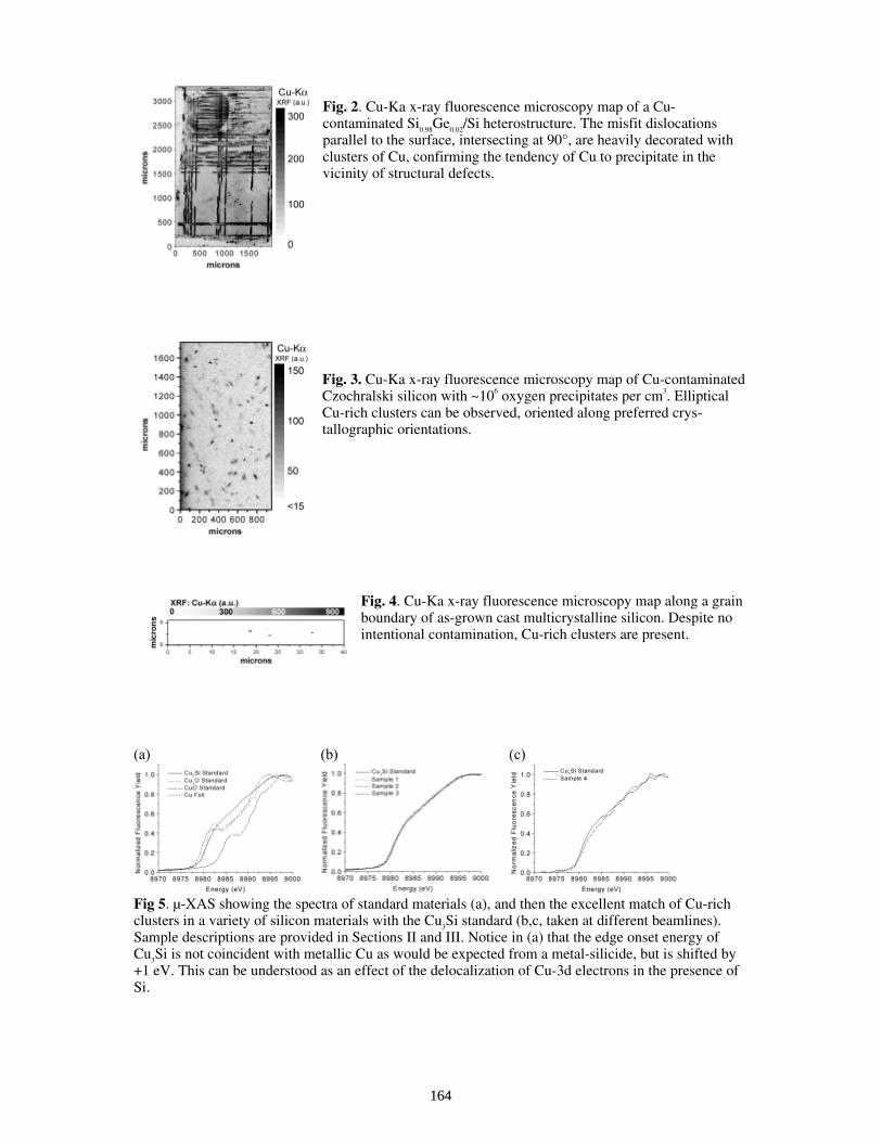
Fig. 2. Cu-Ka x-ray fluorescence microscopy map of a Cu-contaminated Si0.98Ge0.02/Si heterostructure. The misfit dislocations parallel to the surface, intersecting at 90°, are heavily decorated with clusters of Cu, confirming the tendency of Cu to precipitate in the vicinity of structural defects.
Fig. 3. Cu-Ka x-ray fluorescence microscopy map of Cu-contaminated Czochralski silicon with ~106 oxygen precipitates per cm3. Elliptical Cu-rich clusters can be observed, oriented along preferred crys-tallographic orientations.
Fig. 4. Cu-Ka x-ray fluorescence microscopy map along a grain boundary of as-grown cast multicrystalline silicon. Despite no intentional contamination, Cu-rich clusters are present.
(a) (b) (c)
Fig 5. µ-XAS showing the spectra of standard materials (a), and then the excellent match of Cu-rich clusters in a variety of silicon materials with the Cu3Si standard (b,c, taken at different beamlines). Sample descriptions are provided in Sections II and III. Notice in (a) that the edge onset energy of Cu3Si is not coincident with metallic Cu as would be expected from a metal-silicide, but is shifted by +1 eV. This can be understood as an effect of the delocalization of Cu-3d electrons in the presence of Si.
164

Dependence of precipitation behavior of Cu and Ni in CZ and multicrystalline silicon on cooling conditions
A.A.Istratov1, T.Buonassisi1, M.A.Marcus2, T.F.Ciszek3, and E.R.Weber1
1 University of California, Berkeley CA 94720 2 Advanced Light Source, Lawrence Berkeley National Laboratory, Berkeley CA 94720 3 National Renewable Energy Laboratory, Golden, CO 80401; present address: Siliconsultant, P.O. Box 1453, Evergreen, CO 80437
The objective of this study was to investigate the size, chemical state, and spatial distribu-tion of metal clusters formed in substantially different cooling conditions of the samples. All samples were scratched on the back with Fe, Cu, and Ni wires and annealed at 1200°C for 2.5 hours in forming gas (N2+5% H2 ambient). “Slowly cooled” samples were cooled to room tem-perature inside of the furnace. The cooling took 12 hours, the cooling rate was 25-30 K/min in the beginning of the cool, dropping down to 3-8 K/min in the medium temperature range, and to even lower cooling rates by the end of the cool. “Quenched/reannealed” samples were quenched in silicone oil, cleaned in hot acetone to remove oil residues, etched in HF:HNO3 mixture to re-move surface metal-silicides, inserted into a preheated furnace running at 655°C, annealed for 2.5 hours, and then slowly cooled in the furnace within approximately 12 hours. These two an-nealing conditions were combined with two types of samples: CZ samples with approximately 1.5×106 cm-3 of oxygen precipitates, obtained from MEMC (courtesy of R.Falster), and mul-ticrystalline Si samples grown at NREL using float zone technique by Ted Ciszek. Multicrystal-line growth was achieved using heavily dislocated seed. The following four samples were ana-lyzed: (1) a “slowly cooled” CZ sample; (2) a “slowly cooled” mc-FZ-Si sample; (3) A “quenched / reannealed” CZ sample; (4) A “quenched / reannealed” mc-FZ-Si sample.
Although all of these samples were intentionally contaminated with Cu, Ni, and Fe, very low density of iron clusters was found in XRF maps. Therefore, the majority of data presented below are confined to Cu and Ni only. It is known that iron rarely forms precipitates detectable by traditional analytical techniques such as transmission electron microscopy (TEM); the only experimental condition under which large iron-silicide precipitates were observed by TEM in the bulk of silicon samples were experiments with implantation of large doses of iron into silicon with a subsequent anneal (see [1] and references therein). It appears that iron prefers to homoge-neously decorate extended defects rather than to form large metal precipitates. In addition, the relatively low solubility of Fe in single-crystalline silicon at 1200°C, which is at least two orders of magnitude less than Cu or Ni, can be a limiting factor for precipitate size.
In the slowly cooled CZ sample, very few decorated oxygen precipitates were visible in XBIC and Ni/Cu µ-XRF map (Fig. 1). In the slowly cooled mc-FZ-Si samples (Fig. 2), a clear image of grain boundaries was observed in the XBIC map. µ-XRF map of nickel revealed that Ni has very selectively precipitated at some of the grain boundaries. Copper precipitated in much lower concentrations, and copper-related contrasts were barely visible in µ-XRF maps. Even though copper has a higher solubility at the diffusion temperature than nickel, we see a much stronger signal from nickel than from copper. This observation lead us to the following two con-clusions:
First, surface metal silicide, which serves as a source of metals during the high-temperature anneal, acts as a highly efficient sink during cooling. Lets estimate how the surface
165
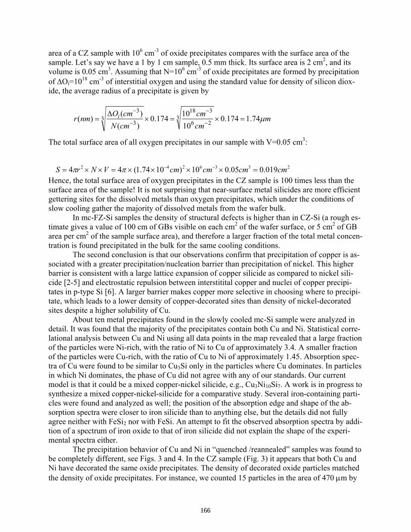
area of a CZ sample with 106 cm-3 of oxide precipitates compares with the surface area of the sample. Let’s say we have a 1 by 1 cm sample, 0.5 mm thick. Its surface area is 2 cm2, and its volume is 0.05 cm3. Assuming that N=106 cm-3 of oxide precipitates are formed by precipitation of ∆Oi=1018 cm-3 of interstitial oxygen and using the standard value for density of silicon diox-ide, the average radius of a precipitate is given by
mcmcm
cmNcmOnmr i µ74.1174.0
1010174.0
)()()( 3
26
3183
3
3=×=×
∆= −
−
−
−
The total surface area of all oxygen precipitates in our sample with V=0.05 cm3:
Hence, the total surface area of oxygen precipitates in the CZ sample is 100 times less than the surface area of the sample! It is not surprising that near-surface metal silicides are more efficient gettering sites for the dissolved metals than oxygen precipitates, which under the conditions of slow cooling gather the majority of dissolved metals from the wafer bulk.
In mc-FZ-Si samples the density of structural defects is higher than in CZ-Si (a rough es-timate gives a value of 100 cm of GBs visible on each cm2 of the wafer surface, or 5 cm2 of GB area per cm2 of the sample surface area), and therefore a larger fraction of the total metal concen-tration is found precipitated in the bulk for the same cooling conditions.
The second conclusion is that our observations confirm that precipitation of copper is as-sociated with a greater precipitation/nucleation barrier than precipitation of nickel. This higher barrier is consistent with a large lattice expansion of copper silicide as compared to nickel sili-cide [2-5] and electrostatic repulsion between interstitital copper and nuclei of copper precipi-tates in p-type Si [6]. A larger barrier makes copper more selective in choosing where to precipi-tate, which leads to a lower density of copper-decorated sites than density of nickel-decorated sites despite a higher solubility of Cu.
About ten metal precipitates found in the slowly cooled mc-Si sample were analyzed in detail. It was found that the majority of the precipitates contain both Cu and Ni. Statistical corre-lational analysis between Cu and Ni using all data points in the map revealed that a large fraction of the particles were Ni-rich, with the ratio of Ni to Cu of approximately 3.4. A smaller fraction of the particles were Cu-rich, with the ratio of Cu to Ni of approximately 1.45. Absorption spec-tra of Cu were found to be similar to Cu3Si only in the particles where Cu dominates. In particles in which Ni dominates, the phase of Cu did not agree with any of our standards. Our current model is that it could be a mixed copper-nickel silicide, e.g., Cu3Ni10Si7. A work is in progress to synthesize a mixed copper-nickel-silicide for a comparative study. Several iron-containing parti-cles were found and analyzed as well; the position of the absorption edge and shape of the ab-sorption spectra were closer to iron silicide than to anything else, but the details did not fully agree neither with FeSi2 nor with FeSi. An attempt to fit the observed absorption spectra by addi-tion of a spectrum of iron oxide to that of iron silicide did not explain the shape of the experi-mental spectra either.
The precipitation behavior of Cu and Ni in “quenched /reannealed” samples was found to be completely different, see Figs. 3 and 4. In the CZ sample (Fig. 3) it appears that both Cu and Ni have decorated the same oxide precipitates. The density of decorated oxide particles matched the density of oxide precipitates. For instance, we counted 15 particles in the area of 470 µm by
2336242 019.005.010)1074.1(44 cmcmcmcmVNrS =××××=××= −−ππ
166

410 µm. Assuming a 70 microns µ-XRF probing depth, we obtain the density of metal precipi-tates of 1.1×106 cm-3, which matches the density of the oxide precipitates. Hence, we conclude that all SiO2 precipitates are metal-decorated. The ratio of Ni counts to Cu counts in this sample was in the range of 0.23 to 0.26, which reasonably matches the ratio of Ni and Cu solubilities. In the mc-Si sample (Fig. 4) all structural defects were beautifully decorated. Ni has strongly deco-rated all grain boundaries and weakly decorated intragranular dislocations. Copper was found on both grain boundaries and dislocations.
The observed strong decoration behavior can be explained as follows. Rapid quench from the annealing temperature prevents metals from diffusion towards the surface silicides. Once the surface silicides are removed by chemical etching and samples are inserted back into preheated furnace running at 655oC, quenched-in metals get mobile and at the same time remain highly su-persaturated. Supersaturation of metals determines the energy gained by a metal when it precipi-tates and therefore the height of potential barrier for precipitation which it can overcome. In such conditions metals can precipitate at sites which would be very unfavorable if the sample were cooled slowly.
In summary, “quenched / reannealed” samples feature much higher density of decorated defects and overall much higher concentrations of Cu and Ni precipitated at structural defects than in the samples which were slowly cooled from 1200oC. In quenched/reannealed samples the detected concentrations of precipitated Cu is greater than that of Ni (which agrees with a higher Cu solubility), whereas in slowly cooled samples the Ni concentration is generally higher than the Cu concentration. We think that this difference is explained by the efficiency of surface sili-cides as a sink for the dissolved metals. Since Cu is a faster diffuser than nickel and since the barrier for nucleation of Cu precipitates is higher than that for Ni, a higher fraction of Cu diffuses out in slowly cooled samples, leaving a relatively high Ni concentration in the bulk. In contrast, in quenched/reannealed samples, where surface silicides are removed and supersaturation ratio (i.e., the ratio of the interstitially dissolved metal concentration to its equilibrium solubility) is sufficient for easy nucleation of Cu precipitates, both Cu and Ni precipitate in the bulk and the ratio of their measured concentrations better reflects the ratio of their solubilities.
Copper has been extensively used for delineation of defects in silicon; the technique is known as copper decoration (see, e.g., [7, 8]). Our results provide a direct evidence that the effi-ciency of this process greatly depends on the cooling regime of the wafer.
The findings of this study contribute to the understanding of the behavior of metal impu-rities during crystal growth. Faster cooling of ribbon/sheet/ingot is likely to lead to a higher den-sity of small metal precipitates. Slow cooling would stimulate formation of a lower density of larger metal precipitates, which are likely to affect the minority carrier diffusion length to a lesser extent than high density of small precipitates. The range of temperatures where the cooling rate gets important includes temperatures where dissolved metals get supersaturated but remain highly mobile, i.e., may include temperatures from 1000oC down to 500oC, depending on the metal. Most cooling regimes used for ingot growth are actually close to what we used in the "slow" cool. Our results suggest that distribution of metals in an mc-Si wafer may be engineered by a heat treatment with a properly designed cooling profile.
1. A. A. Istratov, H. Hieslmair, and E. R. Weber, Appl. Phys. A 70, 489 (2000). 2. M. Seibt, H. Hedemann, A. A. Istratov, F. Riedel, A. Sattler, and W. Schröter, phys. stat. sol. (a) 171, 301 (1999). 3. M. Seibt and W. Schröter, Phil. Mag. A 59, 337 (1989). 4. M. Seibt, M. Griess, A. A. Istratov, H. Hedemann, et al., phys. stat. sol. (a) 166, 171 (1998).
167

5. M. Seibt and K. Graff, J. Appl. Phys. 63, 4444 (1988). 6. C. Flink, H. Feick, S. A. McHugo, W. Seifert, H. Hieslmair, et al., Phys. Rev. Lett. 85, 4900 (2000). 7. T. Yamauchi, Y. Tsumori, T. Nakashizu, H. Esaka, et al. Jpn. J. Appl. Phys. (Letters) 31, L439 (1992). 8. W. C. Dash, J. Appl. Phys. 27, 1193 (1956). FIGURES
500 1000 1500600
8003.000E4
3.500E4
4.000E4
4.500E4
5.000E4
5.500E4
XBIC
500 1000 1500600
8000
40.00
80.00
120.0
160.0
200.0
Ni
500 1000 1500600
8000
60.00
120.0
180.0
240.0
300.0
360.0400.0
Cu
Fig. 1. Maps obtained on slowly cooled CZ samples. Ni and Cu µ-XRF maps were measured with a much larger step size than the beam size. Nearly every Ni precipitate had a small amount of copper in it, and vice versa. The scale on the maps is in microns.
XBIC Cu Ni Fe Fig. 2. Maps obtained on slowly cooled mc-FZ-Si samples: Ni µ-XRF map (top left), Cu µ-XRF map (top right), and XBIC (bottom left). The intensity scale is in arbitrary units (counts).
0 250 5000
250
500
750
1000
microns
mic
rons
10.0012.1614.7917.9821.8726.5932.3439.3247.8258.1570.7185.99104.6127.2154.6188.0228.7278.1338.1411.2500.0
0 250 5000
250
500
750
1000
microns
mic
rons
0350.0700.0105014001750210024502800315035003850420045504900525056005950630066507000
0 250 5000
250
500
750
1000
microns
mic
rons
1.0001.3971.9512.7263.8075.3187.42910.3814.5020.2528.2839.5155.1977.09107.7150.4210.1293.5410.0572.7800.0
0 250 5000
250
500
750
1000
microns
mic
rons
10.0011.4113.0214.8616.9519.3422.0725.1928.7432.7937.4242.6948.7255.5963.4372.3882.5994.23107.5122.7140.0
168

Fig. 3. XBIC (top), Cu (middle) and Ni (bot-tom) maps of a CZ sample diffused with metals at 1200oC, quenched, etched, and annealed again at 655oC. The vertical di-mension of the plots is 0.5 mm.
XBIC Ni µ-XRF Cu µ-XRF Fig. 4. XBIC, nickel µ-XRF, and copper µ-XRF maps of multicrystalline FZ samples which were intention-ally contaminated at 12000C, quenched and re-annealed at 655oC.
0 250 5000
250
500
750
1000
1250
microns
mic
rons
0 250 5000
250
500
750
1000
1250
microns
mic
rons
0
16.25
32.50
48.75
65.00
81.25
97.50
113.8
130.0
146.3
162.5
178.8
195.0
211.3
227.5
243.8
260.0
276.3
292.5
308.8
325.0
0 250 5000
250
500
750
1000
1250
microns
mic
rons
05.00010.0015.0020.0025.0030.0035.0040.0045.0050.0055.0060.0065.0070.0075.0080.0085.0090.0095.00100.0
169
The National Center for Photovoltaics Process Integration Project Brent Nelson, Steven Robbins, and Peter Sheldon National Center for Photovoltaics, National Renewable Energy Laboratory (NREL), Golden, CO 80401-3393, U.S.A. ABSTRACT The research staff of the National Center for Photovoltaics (NCPV) has excelled in increasing solar cell efficiencies and advancing the understanding of photovoltaic-related materials and devices using their existing deposition, processing, and characterization tool base. However, using our existing equipment, it is becoming increasingly difficult to gain new knowledge about important issues related to process sequencing, growth chemistry and kinetics, interface characteristics, and the understanding of how these interfaces affect device performance. This is due in part to the state of our existing tool set, which lacks sufficient in-situ or real-time measurement capabilities, or lacks access to analytical tools where the sample remains in a controlled environment between deposition or processing and measurement. The existing tool set is difficult to upgrade with these capabilities because they are mostly "standalone," which means that they operate independently of each other and without a common substrate size or type. As a result, the NCPV has embarked on a project to provide the infrastructure to allow researchers to gain new knowledge that is difficult—if not impossible—to obtain with existing equipment. This infrastructure consists of providing flexible and robust integration of deposition, processing, and characterization tools via a standardized transfer interface such that samples move between tools in a controlled ambient. Standardization of control and data management software will enhance the utility of the integrated tools. This concept will also requires the cooperation of experts from various material technologies and characterization disciplines to work directly with each other to obtain answers to key scientific and technological questions. Ultimately, it will be this synergistic effort between NREL staff, universities, and the photovoltaic (PV) industry around an integrated tool base that will add to the knowledge base, helping move many PV technologies forward. INTRODUCTION The NCPV has realized the need for more integrated tools for many years 1. The III-V group at NREL has successfully used an integrated metal-organic chemical vapor deposition (MOCVD) chamber, a molecular beam epitaxy (MBE) chamber and a surface science chamber for a number of years. By having integrated deposition and characterization and being able to transfer samples between chamber under ultra-high vacuum (UHV), they have been able to investigate the stability of surfaces 2 and surface reconstruction processes 3 among other things. However, these tools are not integrated with other tools within the NCPV, nor does their tool design facilitate the needs of many of the other PV technologies. While the PV program within the National Renewable Energy Laboratory (NREL) has advanced through focused efforts in materials growth and processing, development of novel device design, and the measurement and characterization of materials and devices, the continued success of the PV program will require full integration of these research areas.
170

Process integration has been the key to the rapid advancement of the integrated circuit industry, which works with similar materials 4. In their case, the various manufacturers came together to develop tool standards and integration schemes that were shared across the industry. This way they were able to drive the direction of tool fabricators to meet the needs of the entire industry. This was not to say they shared all their manufacturing details. A useful analogy might be that they shared kitchen designs, appliances, and ingredients, but not the recipes or family secrets. The integrated circuit industry had two distinctive advantages in accomplishing their process integration, they move around one type of material—silicon wafers—and they have much larger financial resources with which to influence tool development. Other research groups also see the need for process integration within their laboratories. Researchers within the Environmental Molecular Sciences Laboratory at Pacific Northwest National Laboratory have developed a multitask and multiinstrument sample transfer system to integrate a wide range of synthesis and analysis instruments 5. In their system they mount samples to a platen that incorporates heating and measurement capabilities. Similar sample transport/probe/heater assemblies are in use by researchers at Michigan Technology University 6, while Michigan State University has developed a sample transport/probe assembly 7 and the Mississippi State University has developed a sample transport/heater assembly 8. Researchers at the Han-Meitner-Institut in Berlin, Germany have done an outstanding job of not only designing a sample platen, but also integrating an MOCVD and remote UHV chambers by transporting samples via a mobile UHV chamber 9. This system is similar to the NREL III-V group’s integrated tools with the addition of being able to move samples to remote chambers. They have demonstrated that once they establish the correct handling procedure, they can avoid sample contamination completely 10. However, all these systems utilize complex platen designs for small area substrates that have been deemed impractical for the NCPV research needs. The main design goals of the NCPV Process Integration project are to ensure a robust sample transport mechanism, to control the ambient of that sample transfer, to be able to deposit uniformly and reproducibly over areas that are big enough to be meaningful to industry, and to handle a wide variety of sample substrates. THE PATH TO PROCESS INTEGRATION In order to eventually build integrated tools, the NCPV will first design, construct, and test a prototype tool. This prototype tool consists of three major elements: a transport pod, a dock, and a thermal test chamber. This design will be refined and used to construct future tools so that they can be fully integrated. These future tools may be “standalone” or cluster tools with either robotic or track transport mechanisms (Figure 1) depending on the process and analytical needs of a given research area. If the platen is to be moved between tools, it is kept under a vacuum or inert gas while being moved from one tool to another. Standardizing robots and track transport mechanisms for cluster tools—along with heater designs—will also facilitate the construction of future tools. Researchers within the NCPV, as well as their university and industrial collaborators, will have access to these design standards so they can build their tools so they can be integrated to other tools and thus maximize the integrated tool collective. Eventually, researchers NREL will be able build modules to the standard, bring them to NREL, and be able to leverage their new experiment with the existing integrated tool base.
171
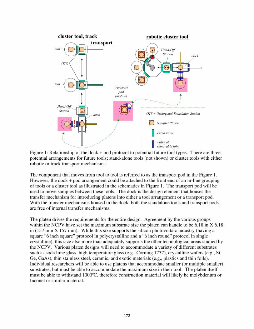
transportpod
(mobile)
dock
robotic cluster toolcluster tool, tracktransport
OTS = Orthogonal Translation Station
Hand-OffStation
OTS
tool
tool
Hand-OffStation
Sample/ Platen
Fixed valve
Valve atremovable joint
dock
Figure 1: Relationship of the dock + pod protocol to potential future tool types. There are three potential arrangements for future tools; stand-alone tools (not shown) or cluster tools with either robotic or track transport mechanisms. The component that moves from tool to tool is referred to as the transport pod in the Figure 1. However, the dock + pod arrangement could be attached to the front end of an in-line grouping of tools or a cluster tool as illustrated in the schematics in Figure 1. The transport pod will be used to move samples between these tools. The dock is the design element that houses the transfer mechanism for introducing platens into either a tool arrangement or a transport pod. With the transfer mechanisms housed in the dock, both the standalone tools and transport pods are free of internal transfer mechanisms. The platen drives the requirements for the entire design. Agreement by the various groups within the NCPV have set the maximum substrate size the platen can handle to be 6.18 in X 6.18 in (157 mm X 157 mm). While this size supports the silicon photovoltaic industry (having a square “6 inch square” protocol in polycrystalline and a “6 inch round” protocol in single crystalline), this size also more than adequately supports the other technological areas studied by the NCPV. Various platen designs will need to accommodate a variety of different substrates such as soda lime glass, high temperature glass (e.g., Corning 1737), crystalline wafers (e.g., Si, Ge, GaAs), thin stainless steel, ceramic, and exotic materials (e.g., plastics and thin foils). Individual researchers will be able to use platens that accommodate smaller (or multiple smaller) substrates, but must be able to accommodate the maximum size in their tool. The platen itself must be able to withstand 1000ºC, therefore construction material will likely be molybdenum or Inconel or similar material.
172
Techniques that are being considered for integrated deposition capabilities include physical vapor deposition techniques (thermal, electron-beam, sputtering, pulsed laser deposition, etc.), chemical bath deposition, vapor transport deposition, as well as chemical vapor deposition (CVD) techniques (MOCVD, hot-wire CVD, and plasma-enhanced CVD). Techniques that are being considered for integrated analytical capabilities include scanning Auger electron spectrometry, X-ray and ultraviolet photoelectron spectrometry, scanning electron microscopy, cathodoluminescence, electron back scattered diffraction, secondary electron imaging, backscattered electron imaging, energy dispersive spectroscopy, X-ray analysis, photoluminescence, time-resolved photoluminescence, Raman, radio frequency photo-conductive decay, thin film analyzer Auger electron spectrometry, scanning tunneling microscopy, atomic force microscopy, electron force microscopy, scanning capacitance microscopy, Fourier transform infra-red spectroscopy, X-ray photoemission spectroscopy, and Kelvin probe measurements. Techniques that are being considered for integrated processing capabilities include ion beam milling, laser and thermal annealing, rapid thermal annealing, and etching. Finally, the integrated circuit industry has learned that the integration of control and data acquisition software is important and time consuming 11. Efforts to create “plug and play” integration of manufacturing tools and data are under way 12 and being addressed as a part of this project. ACKNOWLEDGEMENTS This work is supported by the U.S. DOE under Contract No. DE-AC36-99GO10337. The authors wish to thank the entire NCPV for their support and encouragement in this project. REFERENCES 1 P. Sheldon, Progress in Photovoltaics 8, 77 (2000). 2 W. E. McMahon and J. M. Olson, Journal of Crystal Growth 225, 410 (2001). 3 W. E. McMahon, I. G. Batyrev, J. M. Olson, et al., Physical Review Letters 89 (2002). 4 V. Comello, R&D Magazine 36, 18 (1994). 5 S. Thevuthasan, D. R. Baer, M. H. Englehard, et al., Journal of Vacuum Science &
Technology B 13, 1900 (1995). 6 A. E. Nelson and K. H. Schulz, Review of Scientific Instruments 71, 2471 (2000). 7 E. T. Krastev and R. G. Tobin, Journal of Vacuum Science & Technology a-Vacuum
Surfaces and Films 16, 743 (1998). 8 E. J. Romano and K. H. Schulz, Review of Scientific Instruments 75, 983 (2004). 9 T. Hannappel, S. Visbeck, L. Toben, et al., Review of Scientific Instruments 75, 1297 (2004). 10 P. Vogt, T. Hannappel, S. Visbeck, et al., Physical Review B 60, R5117 (1999). 11 M. Pendleton, Solid State Technology 46, 92 (2003). 12 A. Dugenske, A. Fraser, T. Nguyen, et al., International Journal of Computer Integrated
Manufacturing 13, 225 (2000).
173

CHLORINE FREE TECHNOLOGY FOR SOLAR-GRADE SILICON MANUFACTURING
Strebkov D.S., Pinov A., Zadde V.V., Lebedev E.N., Belov E.P., Efimov N.K., Kleshevnikova S.I.,. INTERSOLARCenter, 2, 1-st Veshnaykovsky proezd, 109456, Moscow, Russia. Tel. (+7095) 171-19-20, fax: (+7095) 170-51-01, E-mail: [email protected] K.Touryan, D. Bleak National Renewable Energy Laboratory (NREL), 1617 Cole Boulevard Golden, Colorado 80401-3393, USA
Due to development of solar energy industry the significant increase of polysilicon feedstock (PSF) production will be required in nearest future[1,2]. That’s why creation of special technology of solar grade polysilicon feedstock production is important problem. Today, semiconductor-grade polysilicon is mainly manufactured using the trichlorosilane (SiHCl3) distillation and reduction. The feed-stock for trichlorosilane is metallurgical-grade silicon, the product of reduction of natural quartzite (silica). This polysilicon production method is characterised by high energy consumption and large amounts of wastes, containing environmentally harmful chlorine based compounds.
In the former USSR the principles of industrial method for production of monosilane and polycrystalline silicon by thermal decomposition of monosilane were founded. The process consists of two stages [3]:
1) Etherification of trichlorosilane for further producing of triethoxysilane proceeding in accordance with the reaction:
SiHCl3 + 3 C2H5OH →catalyst SiH(OC2H5)3 + 3 HCl 2) Catalytic disproportion of triethoxysilane proceeding in accordance with the reaction:
4 SiH(OC2H5)3 → catalyst SiH4 + 3 Si(OC2H5)4 This technology was proved in industrial scale at production of gaseous monosilane and
PSF. We offered new chlorine free technology (CFT). Originality and novelty of the process
were confirmed by Russian and US patent [4,5]. This technology differs by the following: 1. The reaction of metallurgical-grade silicon with ethanol at the 280 °C in the
presence of a catalyst:
Si + 3 C2H5OH catalyst Si(OC2H5)3H + H2
2. The catalyst enchanted disproportion (i. e. simultaneous oxidation and reduction) of triethoxysilane will lead to the production of monosilane and tetraethoxysilane:
4 Si(OC2H5)3H catalyst SiH4 + 3 Si(OC2H5)4
3. Dry ethanol and secondary products such as high purity SiO2 or silica sol can be extracted by hydrolysis of tetraethoxysilane. Ethanol will be returned to Stage 1:
Si(OC2H5)4 + 2H2O → SiO2 + 4 C2H5OH
4. Monosilane purification from admixtures is implemented using less energy demanding methods of condensation and sorption. Silicon proceeding decomposed pyrolytically to pure silicon and hydrogen:
SiH4 850° ÷ 900°C Si + 2 H2 Due to absence of chlorine and chlorinated compounds and unrealizable wastes the
process is ecologically safe. The originality of the CFT is that removing of tetraalcoxysilane from technological cycle doesn’t lead to negative consequences or for technology, or for ecology. This is most important feature of the CFT, which allows to covert tetraethoxysilane into valuable product like stable dispersion of Si dioxide in water – silicasol. By isolation of tetraethoxysilane
174

during hydrolysis, return of ethyl alcohol to direct synthesis of ethoxysilanes and high conversion rate of metallurgical silicon into goods products –PSF, high purity monosilane and silicasol – are ensured. CFT provides a substantial reduction of energy consumption (40 kWh per one kg of polysilicon vs. 250 kWh required for one kg of PSF produced by conventional trichlorosilane method) According to pre-calculations; cost of polysilicon feedstock for large-scale production is not more than 15 USD per 1 kg [6].
During the period from 2000 till 2003 the scientific and design works on creation of theoretical and experimental basis for chlorine free alcoxysilane technology of solar and electronic grade PSF production implemented has been in cooperation and with financial support of NREL. The following works were executed during the period:
Investigations of the process of triethoxysilane production by interaction of metal silicon and ethanol were executed; effective solvent, catalyst and optimal regimes of the process were selected; design of the reactor was also elaborated.
Thermodynamic calculations for possible reaction of tetraethoxysilane hydration were executed. The following reactions are of the most interest:
1. Si(OC2H5)4 + Н2↑ → SiН(OC2H5)3 + C2H5ОН 2. 3Si(OC2H5)4 + Si + 4Н → 4SiН(OC2H5)3 3. 3Si(OC2H5)4 + Si + 2Н2↑ → 4SiН(OC2H5)3 It was found out that these reactions are thermodynamically allowed. • Investigations on tetraethoxysilane hydration by calcium hydride (СаН2) were
implemented. It was determined that the reaction occurs with high conversion tetraethoxysilane to silane level (more than 95%)
• New construction of monosilane pyrolysis apparatus was designed. • Scheme of tetraethoxysilane hydrolysis stage and returning of ethanol into the
process was developed. • Technological schemes of the pilot plant complex for PSF production were
elaborated. During 2003 year, the design documentation for pilot plants complex for solar grade PSF
production using chlorine-free technology with capacity 400 kg per year was created (Phase 2). This work was executed basing on results of previous Phase 1, as well as technical solutions found during the design process.
The aim of creation of the pilot plan complex is as following: • finalizing of separate stages and processes of PSF production • measuring of main parameters of the process for specifying of discharge rates for
raw materials, by-products and energy consumption • finalizing of hardware implementation of the process stages for further design of
bigger capacity apparatus. • accumulation and testing of test samples of PSF aiming determining of its quality
and appropriateness for use in different industries (electronics, solar energy products) • specification of cost of the products (PSF, triethoxysilane, high purity monosilane,
silicasol) • elaboration of initial data for industrial scale design. The elaboration of design documentation was implemented according to the Work
breakdown structure approved by NREL (table 1).
The design works were executed as follows: 1. Preparation and agreement of initial data for design works. 2. Technological schemes for separate pilot installations with determination of
material flows and technological regimes, as well as elaboration of technical requirements for design of control and measurement equipment, for electrical equipment and for non-standard equipment etc.
175

3. Elaboration of correspondent parts of design documentation: control and measurement equipment, technical projects of non-standard equipment, specifications, layout, solutions for the equipment placing, documentation, selection of electrical equipment etc.
Table 1. Work breakdown structure for phase 2.
1. Elaboration of technological documentation for design
1.1. Raw monosilane production through disproportionation of triethoxysilane
1.2. Production of triethoxysilane through direct interaction of metallurgical silicon with ethanol
1.3. Producing of PSF by monosilane pyrolysis (including energy supply)
1.4. Producing of silica sol through hydrolysis of tetraethoxysilane
1.5. Deep purifying of raw monosilane
The project is elaborated according to existing in Russia technological, constructing and
sanitary standards; it foresees arrangements ensuring constructional reliability, fire and explosion safety, population protection and sustainable operation in emergency conditions, as well as environment protection measures
Characteristics of main raw materials for CTF presented in table 2. As main raw materials the metallurgical silicon is used with comparatively low purity and ethanol, which at the stage of silica-sol production is returning to the process.
Table 2.
Name Main parameters
Metallurgical silicon grounded
Mass share of silicon, % - not less than 98,0 Fraction content,% - bigger than 0,5 mm – not more than 5,0
not more than 0,5 – 0,072 mm – not less than 75,0 smaller than 0,072 mm – not more than – 25,0
Ethyl alcohol dehydrated, technological
Mass share of alcohol, % - not less than 98,8 Water content, % - not more than 0,1
Primary goal of any process of PSF production is ensuring of conditions at which the
content of micro admixtures in PSF is minimum, because this determines its suitability for manufacturing of electronic products.
The most important role thus plays micro admixtures of electro active elements, namely elements of III and IV groups of Periodic system (acceptors and donors), which in many respects determine electro physical characteristics of silicon and operational characteristics of electronic devices. Special importance has acceptor admixture of boron since at subsequent PSF processing into monocrystal silicon by floating-zone method and by Chohralski method, the concentration of boron admixture remains constant, in contrast to other elements. The residual level of the boron content determines quality of the production.
In the CTF the removal of boron in technological process occurs at two stages: 1. at purifying of raw triethoxysilane due to linkage of boron in solid nonvolatile
complexes;
176

2. at catalytical disproportionation of triethoxysilane; because of the reaction selectivity the boron and some other elements (phosphorus,arsenic etc.) do not form volatile gaseous hydrides (B2H6, PH3, AsH3 etc.), and their liquid compounds are removed with liquid tetraethoxysilane.
Thank to this the produced PSF has unique electro physical characteristics: specific resistance on boron is higher than 10000 Ω⋅cm, and on donors - higher than 600 Ω⋅cm.
Measures on excluding possibilities of pollution of intermediate and main products during the technological process were undertaken at designing of the CTF. It is achieved by the appropriate choice of constructional materials for the equipment, pipelines, armature, use of minimum quantity of nipples connections, selection of optimum conditions of welding.
The big attention in the project is given to creation of original apparatuses ensuring maximal output of main products. Especially it concerns to the reactor for direct synthesis of raw triethoxysilane in which optimum contact of reacting components: technical silicon, dehydrated ethanol and catalyst – is provided.
Reactor of disproportionate of triethoxysilane it is implemented in such a manner that mixing of input components occurs due to educed gaseous monosilane and does not demand mechanical mixing devices. Thanks to this necessary tightness of the reactor and absence of pollution of gaseous monosilane with impurities from environmental atmosphere is provided. Thus, high conversion of triethoxysilane into monosilane (up to 95 %) in disproportionate reactor is provided. Similar conditions are ensured in the rest non-standard equipment of the CTF.
One of the basic advantages the CTF is ecological safety of production process [7]. First of all, it is ensured by the absence in the technological cycle of aggressive and harmful products such as chlorine, chorus hydrogen and other chlorine-containing products. Moreover, ecological safety of manufacture is ensured by absence of waste gaseous emissions, as well as liquid and solid waste products.
Main products (table 3) for the new method of PSF production are: Monosilane and monosilane mixtures with other gases.
• Electronic grade feedstock silicon. • PSF for PV industry. The technological process allows changing assortment and shares of the products in total
amount depending on market situation. High quality of monosilane and SGPF are confirmed by measurements. The admixtures
presence is at the level of sensitivity of modern instruments. Specific resistance of monocrystalline silicon samples produced by float zone technique is more than 10 000 Ώ.cm, and lifetime of minority carriers is up to 1000 µs.
At the same time there is 24 kg of tetraethoxysilane per 1 kg of monosilane in the yield. To convert it to other useful materials several technologies were elaborated:
As result of hydrolysis of tetraethoxysilane, silica sols are produced; they can be used as coupling agent at manufacturing transfer-molds, for textile and construction materials strengthening, for creation of composite and other new materials. After thermal treating of silica sols SiO2 is obtained; it can be used for manufacturing of optical glass fiber and quartz wares,
Through organ magnesium synthesis of tetraethoxysilane wide used silicone polymers are obtained [8].
By thermal-oxidation of tetraethoxysilane superfine silicon dioxide (white soot) is obtained, it is used as a filler material.
Conclusions 1. Design works on the small-scale pilot plant for PSF with productivity 400 kg / year are
completed. Works on creation and testing of the small-scale pilot plant can be executed within 25 months. Also, the initial data on design of the industrial scale plant with productivity above 100 tones per year and estimated project cost for stages will be developed.
177

2. At creation of industrial scale production the specific energy consumption and cost of production will be reduced in 10 times because of:
- thermal energy recuperation; - increases of productivity of units and devices: - converting of all technological stages into continuous process mode; - decrease of specific number of workers. Table 3. Characteristics of commodities produced
Name Parameters of quality
Main production PSF Specific electric resistance of monocrystal, Ω⋅cm – not less than 10000.
Lifetime of non-uniform carriers, µs, more than 1000
Monosilane
Mass share of elements, %, not more than: В – 6х10-5; Fe - 1х10-4; Ni - 5х10-5; Mn - 1х10-6; Al - 5х10-5; Cu - 1х10-4; Mg - 5х10-5. volume share of oxygen-containing organic admixtures, %, not more than 1х10-3
By-product
Silicasol-30
Content of silicon dioxide (SiO2), %mass – 30. рН of the solution– 7,5 – 9,0. kinematic viscosity at 200С, cst – not more than 20. Density at 200С, kg/m3 – 1200 – 1210.
Triethoxysilane
Main product content, %mass – 99,87. Micro admixtures content, %mass - В – 3х10-7; Fe - 5х10-6; Тi - 1х10-6; Mn - 1х10-6; Al - 1х10-6; Cu - 1х10-7; Mg - 1х10-7; Са - 5х10-6; Сr - 5х10-6.
Tetraethoxysilane
Main product content, %mass – 99,8 Micro admixtures content, %mass - В – 1х10-7; (Ti, Cu, V, Mo, Mn) - 5х10-7; (P, Zn, Pb, Sb, Cr, Co, As, Sn, Bi) - 1х10-6; Mg - 2х10-6; (Са, Fe, Al) - 5х10-6; (Ta, Li, Сd) - 5х10-6.
Capital expenses will be simultaneously reduced due to: - decrease of specific cost of the equipment, instrumentations, armatures, and pipelines; - decrease of specific cost of civil and installation works
References
1. Bernreuter J., The Time Pressure is Enormous, Photon International, September, pp. 26-32, 2001.
2. Maurits J., Polycrystalline Silicon – World Demand and Supply. Eight Workshop on Crystalline Silicon Solar Cell Materials and Processes, NREL, Colorado, August, pp. 10-17, 1998.
3. Strebkov D.S., Pinov A., Zadde V., Tsuo Y.S., Touryan K., Murphy L., Gee J.M., Polysilicon production in the Commonwealth of Independent States. Eight Workshop on Crystalline Silicon Solar Cell Materials and Processes, NREL, Colorado, August, pp. 18-21, 1998
4. Е. Belov, V. Gerlivanov, V. Zadde, S. Kleschevnikova, N. Korneev, E. Lebedev, A. Pinov, Y. Tsuo, E. Ryabenko, D. Strebkov, Е. Chernyshev, Preparation Method for High Purity Silane, Russian Patent No. 2129984 (Priority claimed: June 25, 1998. Publ.: Russian Patent Bulletin No. 13, May 5, 1999).
178

5. Y. Tsuo, Е. Belov, V. Gerlivanov, V. Zadde, S. Kleschevnikova, N. Korneev, E. Lebedev, A. Pinov, E. Ryabenko, D. Strebkov, Е. Chernyshev, Method of High Purity Silane Preparation, US Patent No. 6,103,942 (Publ.:Aug. 15, 2000. Priority claimed:Apr. 8, 1999).
6. Strebkov D.S., Zadde V., Pinov A., Touryan K., Murphy L., Crystalline Silicon Technologies in CIS Countries. 11th Workshop on Crystalline Silicon Solar Cell Materials and Processes, Colorado August, pp.199-207,2001.
7. Tsuo Y.S., Gee J.M., Menna P., Strebkov D.S., Pinov A., Zadde V., Environmentally benign silicon solar cell manufacturing. 2-nd World Conference and Exhibition on Photovoltaic Solar Energy Conversion, 6-10 July, Vienna, Austria, pp.1199-1204, 1998.
8.. Е. Belov, V. Gerlivanov, V. Zadde, S. Kleschevnikova, N. Korneev, E. Lebedev, A. Pinov, Y. Tsuo, E. Ryabenko, D. Strebkov, Е. Chernyshev. International Congress Busines and Investment for Renewable Energy in Russia. 31 May- 4 June, 1999, Moscow, Russia, pp. 22-32.
179
Theoretical study of boron-oxygen complexes in silicon
Mahdi Sanati and Stefan K. Estreicher
Physics Department, Texas Tech University, Lubbock, TX 79409-1051 Abstract: The carrier lifetime in boron-doped Czochralski (CZ) silicon is strongly reduced by illumination or by applying forward bias voltage. This leads to a significant loss in solar cell efficiency. The culprit is suspected to be a (still unidentified) boron-oxygen complex. Very little information is available on the nature of this defect, or of any B-O interactions in Si. We are using a first-principles method to study systematically all the stable and metastable complexes involving B and O in silicon, in order to identify possible candidates and rule out others. 1. Introduction The efficiency of boron-doped Czochralski (CZ) silicon solar cells decreases by up to 10% (relative) under illumination or minority-carrier injection in the dark [1,2]. This is related to the formation of a recombination center believed to contain boron and oxygen. A combination of temperature- and injection-dependent lifetime spectroscopy (TDLS and IDLS) studies in standard boron-doped CZ-Si has led to the identification of the electrically-active level of the defect in the upper half of the band gap [3]. However, the concentration of this defect is very low and its structure and formation mechanism are unknown. In a recent experiment, Bothe et al.[4] have shown that the formation of the metastable boron-oxygen complex is directly related to the total recombination rate, and that the degradation in solar cell efficiency already starts at extremely low minority-carrier concentrations. They suggested that the formation of the metastable boron-oxygen complex is a recombination-enhanced process [4]. This defect has been the subject of intense debate during the 2003 Silicon Workshop in Vail. In this paper, we report preliminary results of systematic first-principles calculations aimed at identifying this unknown boron-oxygen complex, which we label XOB. The experimental information about XOB is limited to the following. (1) It exists in concentrations (~1011 cm-3) very much lower than those of substitutional boron (Bs) and interstitial oxygen (Oi), which are some 7 orders of magnitude higher. Thus, XOB could be a metastable configuration of some Bs,Oi or Bs,Oi,Oi complex, or involve the much less abundant interstitial boron (Bi), and/or a native defect (self-interstitial I and/or a vacancy V), etc. (2) Since the formation of XOB is triggered by e−-h+ recombination (but not a change of charge state [4]), XOB is likely a metastable complex which is electrically inactive in one configuration and a lifetime killer in another. (3) XOB does not appear to occur in Al- or Ga-doped samples. Because of the lack of quantitative experimental data (number and type of elements, symmetry, local vibrational modes, etc.), first-principles theory by itself cannot prove beyond doubt which defect is responsible. However, it can identify complexes containing combinations of B and O, predict their structures, binding energies, electrical activity, and other properties, and compare those to the corresponding Al-O and Ga-O complexes. This provides leads to experimentalists on how to generate high-enough concentrations of the defect for positive identification or avoid its formation altogether. Additional theoretical research could involve the possibility of H passivation for example. In diatomics [5], the largest to smallest bond strengths are B-O (~8.1eV), Si-O (~8.0eV), Si-Si (~6.2eV) , Al-O (~5.1eV), and Ga-O (~3.5eV). Although we are not dealing here with diatomics, these numbers suggest that, in Si, covalent B-O interactions are more likely to occur than Al-O or Ga-O interactions.
180

Schmidt and Bothe [6] measured the correlation between the concentration of XOB and that of B and O. They concluded that XOB is composed of one Bs and two Oi’s and proposed a defect reaction model based on the fast-diffusing oxygen dimer. Their Bs,Oi,Oi− complex is based on the smaller covalent radius of the B atom with respect to the Si host atom. Although this reasoning includes important features, the model cannot quantify the (possibly strong) covalent interactions between the elements involved. Recent theoretical studies have focused on the Bi,Oi complex. The ab-initio calculations of Ohshita et al. [7] have shown that such a complex is stable when a Si atom sits between the Bi and Oi atoms. Further calculations of energy levels have shown that this defect has a partly occupied deep level in the band gap [7]. In independent ab-inito calculations, Adey et al. [8] found a binding energy of 0.6eV for this defect. The ingredients in our systematic search for XOB include Bs
− or Bi0 and (neutral) Oi or Oi,Oi.
Indeed, studies of the kinetics of O-related thermal donor formation [9] imply that the formation of the Oi,Oi pair is energetically favorable and does occur as soon as the temperature is high enough (~350oC) for isolated Oi to migrate. More importantly, the Oi,Oi pair diffuses much faster than isolated Oi and is therefore likely to interact with dopants and defects. A dozen configurations involving combinations of these ingredients are a priori possible. Many more defect structures have to be considered if one adds a third ingredient, such as a self-interstitial or a vacancy. Preliminary results of our ongoing systematic search for XOB are presented below. 2. Theoretical background Our results are obtained with first-principles, self-consistent density functional theory coupled to molecular-dynamics simulations, as implemented in the SIESTA package [10]. The host crystal is represented by periodic 64-host atom supercells. The k-points sampling is a 2×2×2 Monkhorst-Pack [11] mesh. The exchange-correlation potential is that of Ceperley-Alder [12] parameterized by Perdew-Zunger [13]. Ab-initio pseudopotentials in the Kleinman-Bylander [14] form are used. The basis sets for the valence states are (numerical) linear combination of atomic orbitals. We use double-zeta basis for B and O and add polarization functions for Si, Al, and Ga. The geometries are optimized with conjugate gradients. The energies of the final configurations are compared to those of the dissociated species to get binding energies. Band-structure calculations of the most stable structures will give qualitative information about the electrical activity of the various complexes. The vibrational spectra and phonon densities of state will be obtained from linear response theory. This will allow the calculation of the local vibrational modes associated with the defects, as well as the temperature dependence of the binding energies (vibrational free energy and configuration entropy terms) [15]. 3. Results The Bs,Oi− complex: The defect we considered first consists of Bs in the −1 charge state and neutral Oi. The most stable configuration of the Bs,Oi− complex has Oi bridging a Si-Si bond adjacent to B, that is Si-Oi-Si-Bs. However, its binding energy (at T=0K) relative to isolated Bs
− and Oi is only −0.28eV. Since binding energies become smaller [15] at T>0K (mostly because of the configurational entropy term), this defect is unlikely to form at or above room temperature. The metastable configuration nearest in energy has Oi bridging one of the Bs-Si bonds (Si-Oi-Bs). Its binding energy is +0.15eV, meaning that it is less stable (even at T=0K) than the dissociated impurities. Therefore, Bs
− and Oi should not form pairs in Si.
181

The Bs,Oi,Oi− complex: The stable configuration of the Bs,Oi,Oi− complex (Fig. 1, left) has each of the two Oi bridging a Si-Si bond adjacent to Bs
−, with one common Si nearest neighbor. Its binding energy relative to isolated Bs
− and Oi,Oi is −0.49eV at T=0K. The metastable configuration nearest in energy (Fig. 1, middle) also has the Oi’s bridging a Si-Si bond adjacent to Bs
−, but have no common Si neighbor. Its binding energy at T=0K is −0.28eV. Figure 1 right shows the configuration suggested by Schmidt and Bothe [6]. We find it to be unstable, with a binding energy of +0.12eV at T=0K.
Fig. 1: The stable (left) and metastable (middle) configurations of Bs,Oi,Oi−. The structure proposed in Ref. [6] (right) is less stable than the dissociated species.
The Bi,Oi0 complex: The most stable (Eb = −0.47eV) and energetically nearest metastable (Eb
= −0.20eV) configurations of the complex formed with Bi0 and Oi are shown in Fig. 2 (left and
right, respectively). If we use Troxell and Watkins’ 0.6eV migration energy [16] for Bi, we find an activation energy for dissociation of 1.07eV for the stable configuration. This is in good agreement with the value deduced from isothermal anneals [17], EA=1.2±0.1eV and with the 1.2eV calculated by Adey et al. [8]. Thus, we find that Oi does form a stable complex with Bi, and that a metastable configuration exists.
Fig. 2: The stable (left) and metastable (right) configurations of the Bi,Oi0 complex. The Bi,Oi,Oi0 complex: The last defect we considered so far consists of Bi
0 and the Oi,Oi dimer. We find two structures with comparable binding energies relative to isolated Bi
0 and Oi,Oi: −0.59eV (Fig. 3, left) and −0.53eV (Fig.3, right). More research is under way.
182

Fig. 3: The two nearly degenerate configurations of the Bi,Oi,Oi0 complex. 4. Summary We have calculated a dozen configurations for complexes containing Bs
− or Bi0 and Oi or
Oi,Oi. The Bs,Oi− complex is not likely to form, but a couple of candidates for the XOB defect involving Bi
0 have emerged. Several more structures involving V and/or I must be tested, then the band structures and thermodynamics of the most stable complexes will be calculated. Acknowledgements This work is supported in part by NREL and the R.A. Welch Foundation. References 1. H. Fischer and W. Pschunder, Proc. 10th IEEE Photovoltaic Specialists Conf. (IEEE, New York, 1973), p. 404. 2. J. Knobloch, S.W. Glunz, V. Henninger, W. Warta, W. Wettling, F. Schomann, W. Schmidt, A. Endrös, and K.A. Münzer, Proc. 13thEuropean Photovoltaic Solar Energy Conference, Nice, France, (Stephens, Bedford, 1995), p. 9. 3. S. Rein and S.W. Glunz, Appl. Phys. Lett. 82, 1054 (2003). 4. K. Bothe, R. Hezel, and J. Schmidt, Appl. Phys. Lett. 83, 1125 (2003). 5. Handbook of Chemistry and Physics, ed. D.R. Lide (CRC, Boca Raton, 2001) 6. J. Schmidt and K. Bothe, Phys. Rev. B 69, 024107 (2004). 7. Y. Ohshita, T. Khanh Vu, and M. Yamaguchi, J. Appl. Phys. 91, 3741 (2002). 8. J. Adey, R. Jones, P.R. Briddon, and J.P. Goss, J. Phys. C 15, 2851 (2003). 9. Oxygen in Silicon, ed. F. Shimura, Semic. & Semimet. Vol. 42, (Academic, San Diego, 1994). 10. D. Sánchez-Portal, P. Ordejón, E. Artacho, and J.M. Soler, Int. J. Quant. Chem. 65, 453 (1997); E. Artacho, D. Sánchez-Portal, P. Ordejón, A. García, and J.M. Soler, Phys. Stat. Sol. (b) 215, 809 (1999). 11. H.J. Monkhorst and J.D. Pack, Phys. Rev. B 13, 5188 (1976). 12. D.M. Ceperley and B.J. Alder, Phys. Rev. Lett. 45, 566 ( 1980). 13. S. Perdew and A. Zunger, Phys. Rev. B 32, 5048 (1981). 14. L. Kleiman and D.M. Bylander, Phys. Rev. Lett. 48, 1425 (1982). 15. S.K. Estreicher, M. Sanati, D. West, and F. Ruymgaart, Phys. Rev. B (to be published). 16. J.R. Troxell and G.D. Watkins, Phys. Rev. B 22, 921 (1980) 17. P.M. Mooney, L.J. Cheng, M. Suli, J.D. Gerson, and J.W. Corbett, Phys. Rev. B 15, 3836 (1977).
183

Temperature-dependence of the dissociation energy of copper pairs in Si
Damien West, M. Sanati, and Stefan K. Estreicher Physics Department, Texas Tech University, Lubbock, TX 79409-1051
Abstract: The dissociation energy of the substitutional-interstitial copper pair Cus,Cui in Si calculated at T = 0K differs by almost 30% from the dissociation enthalpy measured around 400K. We show here that this dissociation energy can be calculated from first principles as a function of temperature by including the vibrational free energy and the configurational entropy contribution. The resulting prediction is within the experimental error bar. 1. Introduction
First-principles theoretical studies of defects in semiconductors predict accurate defect configurations, energetics, local vibrational modes, and a few other quantities. However, these calculations ignore free energies and are therefore strictly valid only at T = 0K. We have recently proposed [1,2] a systematic way to calculate (harmonic) vibrational free energies at constant volume in the same supercells as those used for the traditional defect studies. By adding any additional contributions analytically, such as the configurational entropy, we can calculate the temperature dependence of the energetics of defects up to at least 800K. Extending T = 0K calculations to finite temperatures has only been done in a few instances. The free energies of native defects have been calculated from thermodynamic integration, a technique which provides the total free energy relative to a known reference system [3]. In general, the results are in good agreement with other theoretical methods and experiment. However, the thermodynamic integration method requires extensive Monte Carlo or molecular-dynamics simulations at fixed temperatures and the knowledge of the free energy of a reference system. However, the vibrational Helmholtz free energy can be calculated directly if the phonon density of states (pDoS) is known. This was recently achieved by averaging the eigenvalues of the (harmonic) dynamical matrix, which was calculated from first-principles using density-functional perturbation theory [1]. The other free energy contributions can be included or estimated analytically [2]. This approach was used recently to calculate the vibrational free energy of native defects in Si supercells [4]. In this paper, we focus on the dissociation energy of the Cus,Cui pair [5,6] in Si. After a brief discussion of the methodology, the temperature dependence of the energy is shown to depend critically on the configurational entropy term. The results match the experimental values measured at the same temperature. Methodology
The (ground state) electronic problem is solved with self-consistent first-principles molecular-dynamics simulations based on local density-functional theory. ‘First-principles’ means that none of the input parameters is fitted to an experimental database. Our calculations are performed with the SIESTA [7,8] code. The exchange-correlation potential is that of Ceperley-Alder [9] as parameterized by Perdew and Zunger [10]. Norm-conserving pseudopotentials in the Kleinman-Bylander [11] form remove the core regions from the calculations. The basis sets for
184

the valence states are linear combinations of numerical atomic orbitals. In the present calculations, double-zeta sets are used for most host atoms. Cu and the Si atoms that are not near-perfectly sp3 hybridized have an additional set of d functions. The charge density is projected on a real-space grid with an equivalent cutoff of 150Ry to calculate the exchange-correlation and Hartree potentials. Other authors use plane-wave basis sets for the valence states, which affects the choice of pseudopotential and other details of the computations. The crystal is approximated by 64 to 216 host atoms periodic supercells. The energetics at T = 0K are obtained with a 2×2×2 Monkhorst-Pack [12] k-point mesh. The entire dynamical matrix must be calculated in order to obtain the pDoS. We use linear response theory [13] to calculate the (harmonic) dynamical matrix at T = 0K. This calculation is done with k=0 only. This restriction substantially reduces the size of the computation, and the impurity-related local vibrational modes (LVMs) calculated [13] in this way are remarkably reliable, typically within 2% of the ones measured at low temperatures. The constant-volume and harmonic approximations work very well at low temperatures but become increasingly questionable as T rises. However, theses approximations can be used up to at least 800K [2] in materials such as Si. The eigenvalues of the dynamical matrix of a 64-atoms cell gives 192 normal modes, including the three translational modes at ω=0. The Fourier transform of the dynamical matrix can be evaluated at many q points along various directions of the supercell's Brillouin zone. Each q point generates a new set of frequencies. We typically use some 90 q points, thus producing over 17,000 frequencies. The resulting phonon pDoS g(ω) allows the calculation of the vibrational Helmholtz free energy Fvib. in the harmonic approximation.
ωω∫∞
=0
BBvib. d)g(T)ω/2ksinh(lnTk(T)F
Fvib.(T = 0K) is the total zero-point energy of the system. Knowing Fvib.(T) allows the calculation of the specific heat Cv, which can be compared to the measured Cp. These comparisons [2] show that this approach is very good up to at least 800K. The copper pair in Si
Cus,Cui pairs form when a thin copper layer is deposited on the surface of a Si sample, which is then annealed at 600-1,000 oC and quenched. Most of the copper that diffuses into the bulk is interstitial Cui at tetrahedral interstitial sites. A small fraction of it finds a vacancy and becomes substitutional Cus. At low temperatures, Cus,Cui pairs are seen by photoluminescence and deep-level transient spectroscopy (for details and references, see [5]). The pair has C3v symmetry and consists of Cus weakly bound to Cui, which is near one of the four adjacent T sites. The dissociation enthalpy of the pair (measured [6] in the temperature range 333-417K) is found to be Ed = 1.02±0.07eV. Since the measured migration barrier of Cui (in the range 240-380K) is Em
= 0.18±0.02eV [14], the measured binding enthalpy is Eb = 0.84±0.09eV. But the binding energy calculated at 0K [5] (potential energy difference between the pair and the dissociated species) is 1.16eV, quite a bit larger than the measured value. The vibrational free energy is straightforward to calculate from Eq. (1). One needs to know the pDoS’s of the perfect supercell and those of supercells containing the Cus,Cui pair, isolated Cui and isolated Cus. The configurational entropy must be obtained from realistic concentrations of the various defects involved. We assume that the sample contains N Si atoms (and therefore N
185

tetrahedral interstitial and N substitutional sites), ni Cui’s and ns Cus’s. In the experimental work [6], N = 5×1022 cm-3 and ni = 2×1015 cm-3. A reasonable estimate [15] for ns is 2×1012 cm-3. We assume that at high temperatures, the sample contains ni isolated Cui’s and ns isolated Cus’s. At low temperatures, we have ns Cus,Cui pairs and (ni-ns) isolated Cui’s. All we need is a count of the number of possible configurations at low (ΩLT ) and high (ΩHT) temperatures. We find
)!4()!()!4(
)!(!!4LT
sisi
s
ss
s
nnNnnnN
nNnNn
−−−−
−=Ω
.)!3(!
)!4()!(!
!HT
si
s
ss nnNninN
nNnN
−−−
−=Ω
The difference in configurational entropy per copper pair, ∆Sconf = kB log (ΩLT/ΩHT)/ns, becomes ∆Sconf. = kBlog(4ni/N)−3ns/ni. Thus, the contribution of T∆Sconf. to the free energy at the dissociation temperature of 373K is 0.22eV, and the calculated binding energy becomes Eb(373K) = 1.16-0.22 = 0.94eV, within the error bar of the experiment. The vibrational free energy correction is small. The configurational entropy dominates the temperature dependence. The binding energy is plotted as a function of temperature in Fig. 1.
Fig. 1: Calculated binding energy Eb = ∆Etot. of the Cus,Cui pair in Si vs. temperature. Dashed curve = contribution of the vibrational free energy only; solid curve = total
(vibrational + configurational) free energy. The measured dissociation enthalpy Ed = 1.02±0.07eV (horizontal dashed lines) leads to a measured Eb = Ed - Em = 0.84±0.09eV.
The calculated binding energy varies with temperature because the dissociated species have distinct vibrational free energies and configurational entropies. However, within the range of temperatures quoted in the experimental work (333-417K), the change in vibrational free energy is very small and T∆Sconf. = 0.05eV, less than the experimental error bar (0.07eV).
186

Summary
First-principles theoretical studies of defects in periodic supercells are extended to finite temperatures. The most computer-intensive part is the calculation of the (harmonic) dynamical matrix, which is obtained within linear response theory. Its eigenvalues allow the pDoS and therefore the Helmholtz free energy to be calculated. By including configurational entropies (and other contributions), the energies of defects can be calculated at finite temperatures. Perfect cell results show that the vibrational free energies are accurate up to at least 800K. The binding energy of the Cus,Cui in Si is calculated as a function of temperature. The vibrational free energy at 400K gives a correction of only about 0.05eV, but the configurational entropy contributes almost 0.25eV. Thus, the binding energy calculated at T = 0K (potential energy difference between the pair and the dissociated species) is off by nearly 0.30eV at 400K, temperature at which the dissociation enthalpy has been measured. Acknowledgements
This work is supported in part by NREL and the R.A. Welch Foundation. References
[1] M. Sanati and S.K. Estreicher, Sol. St. Comm. 128, 181 (2003); Physica B 340-342, 630 (2003) [2] S.K. Estreicher, M. Sanati, D. West, and F. Ruymgaart, submitted to Phys. Rev. B [3] M. Kaczmarski, R. Rurali, and E. Hernández, Phys. Rev. B (in print). [4] O.K. Al-Mushadani and R.J. Needs, Phys. Rev. B 68, 235205 (2003) [5] S.K. Estreicher, D. West, J. Goss, S. Knack, J. Weber, Phys. Rev. Lett. 90, 035504 (2003) [6] A.A. Istratov, H. Hieslmair, C. Flink, T. Heiser, and E.R. Weber, Appl. Phys. Lett. 71, 2349 (1997) [7] D. Sánchez-Portal, P. Ordejón, E. Artacho, J.M. Soler, Int. J. Quant. Chem. 65, 453 (1997) [8] E. Artacho, D. Sánchez-Portal, P. Ordejón, A. García, and J.M. Soler, Phys. Stat. Sol. (b) 215, 809 (1999) [9] D.M. Ceperley and B.J. Alder, Phys. Rev. Lett. 45, 566 (1980) [10] S. Perdew and A. Zunger, Phys. Rev. B 32, 5048 (1981) [11] L. Kleiman and D.M. Bylander, Phys. Rev. Lett. 48, 1425 (1982) [12] H.J. Monkhorst and J.D. Pack, Phys. Rev. B 13, 5188 (1976) [13] J.M. Pruneda, S.K. Estreicher, J. Junquera, J. Ferrer, and P. Ordejón, Phys. Rev. B 65, 075210 (2002) [14] A.A. Istratov, C. Flink, H. Hieslmair, E.R. Weber, and T. Heiser, Phys. Rev. Lett. 81, 1243 (1998) [15] E.R. Weber, private communication.
187
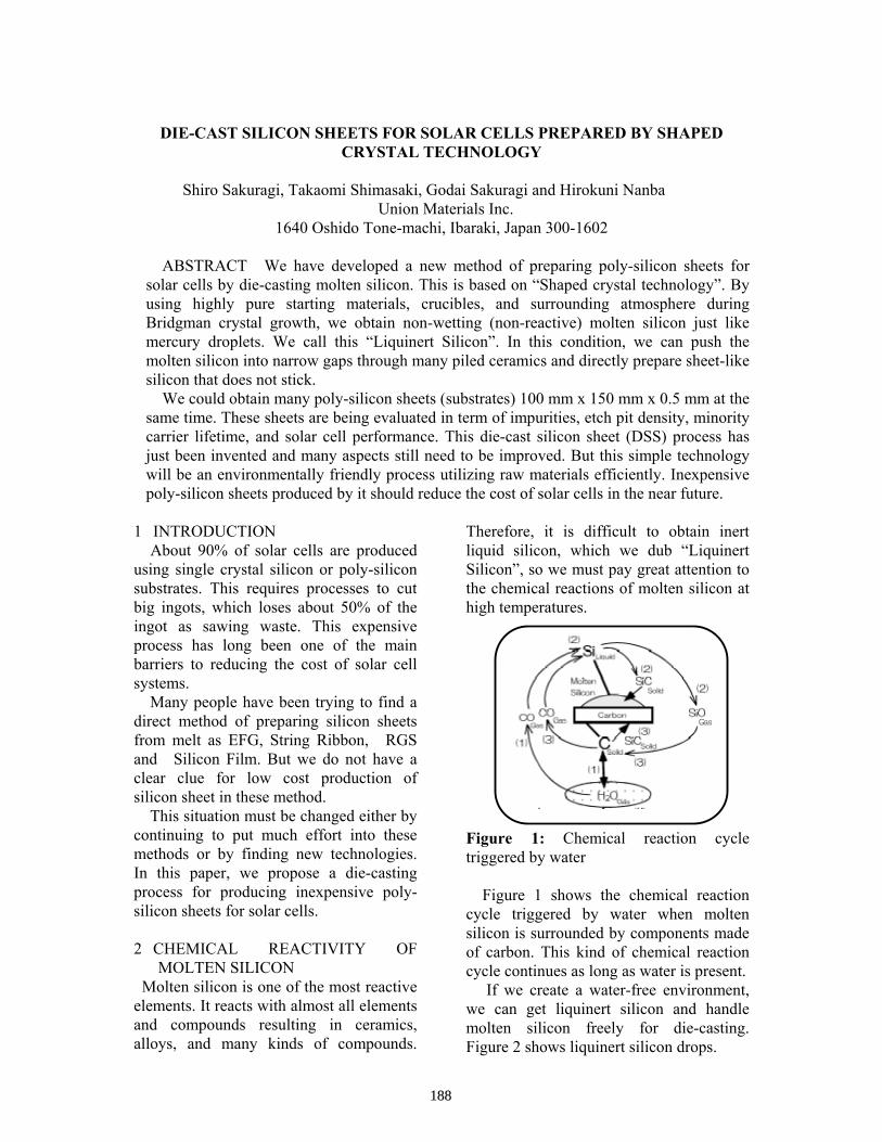
DIE-CAST SILICON SHEETS FOR SOLAR CELLS PREPARED BY SHAPED CRYSTAL TECHNOLOGY
Shiro Sakuragi, Takaomi Shimasaki, Godai Sakuragi and Hirokuni Nanba
Union Materials Inc. 1640 Oshido Tone-machi, Ibaraki, Japan 300-1602
ABSTRACT We have developed a new method of preparing poly-silicon sheets for
solar cells by die-casting molten silicon. This is based on “Shaped crystal technology”. By using highly pure starting materials, crucibles, and surrounding atmosphere during Bridgman crystal growth, we obtain non-wetting (non-reactive) molten silicon just like mercury droplets. We call this “Liquinert Silicon”. In this condition, we can push the molten silicon into narrow gaps through many piled ceramics and directly prepare sheet-like silicon that does not stick.
We could obtain many poly-silicon sheets (substrates) 100 mm x 150 mm x 0.5 mm at the same time. These sheets are being evaluated in term of impurities, etch pit density, minority carrier lifetime, and solar cell performance. This die-cast silicon sheet (DSS) process has just been invented and many aspects still need to be improved. But this simple technology will be an environmentally friendly process utilizing raw materials efficiently. Inexpensive poly-silicon sheets produced by it should reduce the cost of solar cells in the near future.
1 INTRODUCTION About 90% of solar cells are produced using single crystal silicon or poly-silicon substrates. This requires processes to cut big ingots, which loses about 50% of the ingot as sawing waste. This expensive process has long been one of the main barriers to reducing the cost of solar cell systems. Many people have been trying to find a direct method of preparing silicon sheets from melt as EFG, String Ribbon, RGS and Silicon Film. But we do not have a clear clue for low cost production of silicon sheet in these method.
This situation must be changed either by continuing to put much effort into these methods or by finding new technologies. In this paper, we propose a die-casting process for producing inexpensive poly-silicon sheets for solar cells.
2 CHEMICAL REACTIVITY OF
MOLTEN SILICON Molten silicon is one of the most reactive elements. It reacts with almost all elements and compounds resulting in ceramics, alloys, and many kinds of compounds.
Therefore, it is difficult to obtain inert liquid silicon, which we dub “Liquinert Silicon”, so we must pay great attention to the chemical reactions of molten silicon at high temperatures.
Figure 1: Chemical reaction cycle triggered by water
Figure 1 shows the chemical reaction cycle triggered by water when molten silicon is surrounded by components made of carbon. This kind of chemical reaction cycle continues as long as water is present.
If we create a water-free environment, we can get liquinert silicon and handle molten silicon freely for die-casting. Figure 2 shows liquinert silicon drops.
188
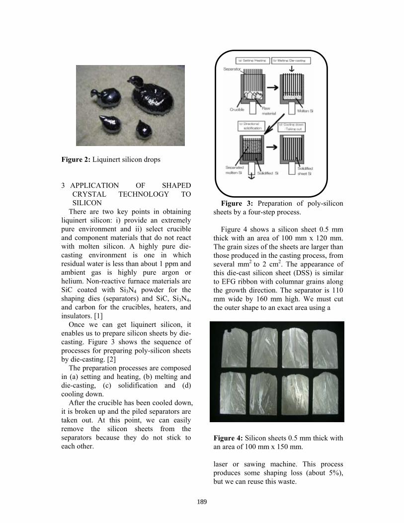
Figure 2: Liquinert silicon drops 3 APPLICATION OF SHAPED
CRYSTAL TECHNOLOGY TO SILICON
There are two key points in obtaining liquinert silicon: i) provide an extremely pure environment and ii) select crucible and component materials that do not react with molten silicon. A highly pure die-casting environment is one in which residual water is less than about 1 ppm and ambient gas is highly pure argon or helium. Non-reactive furnace materials are SiC coated with Si3N4 powder for the shaping dies (separators) and SiC, Si3N4, and carbon for the crucibles, heaters, and insulators. [1]
Once we can get liquinert silicon, it enables us to prepare silicon sheets by die-casting. Figure 3 shows the sequence of processes for preparing poly-silicon sheets by die-casting. [2]
The preparation processes are composed in (a) setting and heating, (b) melting and die-casting, (c) solidification and (d) cooling down.
After the crucible has been cooled down, it is broken up and the piled separators are taken out. At this point, we can easily remove the silicon sheets from the separators because they do not stick to each other.
Figure 3: Preparation of poly-silicon
sheets by a four-step process.
Figure 4 shows a silicon sheet 0.5 mm thick with an area of 100 mm x 120 mm. The grain sizes of the sheets are larger than those produced in the casting process, from several mm2 to 2 cm2. The appearance of this die-cast silicon sheet (DSS) is similar to EFG ribbon with columnar grains along the growth direction. The separator is 110 mm wide by 160 mm high. We must cut the outer shape to an exact area using a Figure 4: Silicon sheets 0.5 mm thick with an area of 100 mm x 150 mm. laser or sawing machine. This process produces some shaping loss (about 5%), but we can reuse this waste.
189

4 EVALUATIONS OF DIE-CAST
SILICON SHEETS
These die-cast silicon sheets were evaluated in terms of impurity content, etch pit density (EPD), minority carrier lifetime, and solar cell performance.
4-1 Impurity analysis of die-cast silicon sheet
We used semiconductor grade silicon as the raw material in this study. The impurity content was very low: down to the 1012/cm3 level. During die-casting, there is a possibility of contamination by metallic impurities, oxygen (O), carbon (C), and nitrogen (N). We analyzed these impurities in DSS samples by glow discharge mass spectroscopy (GDMS) and secondary ion mass spectroscopy (SIMS).
Elemen t
Fe
Ni
Co
Cr
O
C
N
BaySix EFG DSS- 1 DSS- 2
4 .0 x1 0 14 6 .0 x1 0 1 4 1 ~4 x1 0 1 43 .9 x1 0 1 7
8 .2 x1 0 15
1 .2 x1 0 1 5
5 .2 x1 0 1 6
1 .0 x1 0 18
1 .1 x1 0 1 8
2 .1 x1 0 18
1 .1 x1 0 1 8
4 .5 x1 0 1 7
<2 x1 0 1 7
<1 x1 0 1 4<3 x1 0 1 4
2 .1 x1 0 13 1 .7 x1 0 1 2
1 .0 x1 0 13 1 .7 x1 0 1 2
5 x1 0 17 <1 0 1 7
<1 0 17
(cm -3 ) (cm- 3 ) (cm -3 ) (cm -3 )
<1 x1 0 1 3
<3 x1 0 1 3
Table 1: Impurity concentrations of
three types of poly-silicon materials. [3] Table 1 shows typical impurity
concentrations of three types of poly-silicon materials, BaySix, EFG and DSS samples. DSS-1 is a heavily contaminated sheet and DSS-2 is a normal one. It is known that the threshold value of metallic impurity concentration affects the performance of solar cells.
In Table 1, Fe, Co, and Cr concentrations of DSS-1 were reduced from 1016–17/cm3 to 1013–14/cm3 in DSS-2 to become comparable with the level for
BaySix and EFG ones. On the other hand, O, C, and N concentrations of DSS-2 were larger (1018/cm3) than in BaySix and EFG.
4-2 Etch pit density
Poly-crystalline silicon contains many types of grown-in defects, which shorten the carrier lifetime and reduce the performance of solar cells. We measured DSS’s etch pit density (EPD), which exhibited a variety of features. Figure 5 shows one example at a growth rate of 60 mm/hour. The EPD is around 104/cm2. The EPD value may depend on the growth rate, but more information is required about the correlation between EPD and growth conditions.
Figure 5: Example EPD Photograph for a growth rate of 60 mm/hour. 4-3 Carrier lifetime measurement The minority carrier lifetime (CLT) of a silicon substrate is an indicator of solar cell performance. We measured CLTs of our samples by the microwave photoconductivity decay (µ-PCD) method.
The average CLT of as grown sample was 0.13 µs and that of heat-treated at 1100°C was 0.4 µs. These values indicate that the as-grown sample had a low carrier lifetime, which was improved by thermal treatment. 4-4 Solar cell preparation Using DSS samples with CLT values about 0.2 µs, solar cells were prepared at the University of Stuttgart. The samples were polished and etched on both surfaces. The emitter process starts with spinning a phosphorous-containing paste on the samples. Then phosphorous diffuses into
190

the front surface during laser beam annealing. After the leftover paste has been removed using an HF-dip, the process continues by evaporating the front and back contacts. The process finishes with a silicon nitride antireflection coating being deposited at 400°C by plasma deposition.
The highest cell performance to date of DSS made by this process was 5.6%, as shown in Fig 6.
Figure 6: Solar cell prepared with DSS at the University of Stuttgart. 5 DISCUSSION
The short carrier lifetime in our DSS samples shows there are fundamental defects affecting it. In Table 1, Fe, Co, and Cr concentrations in DSS-2 are comparable with other types of poly-silicon. The CLT value is changed from 0.13 to 0.4 µs by heat treatment. This suggests that the recombination capability of impurities was modified by 1100°C thermal processing. The Fe, Co, and Cr impurities formed pairs with boron, such as FeB, in silicon. This kind of metal-boron pair becomes a strong recombination center resulting in a short carrier lifetime. McHugo et al. have observed these impurities precipitate and stabilize at some dislocation sites or grain boundaries on the nanometer scale. [4] In the precipitated area, a low light–induced current (low performance) was detected, but no impurities were observed in a high light–induced current area.
The origin of short CLT in DSS samples is likely to be some complexes of impurities with thermal defects. Therefore, we must improve the growth conditions of DSS during directional solidification. 6 SUMMARY
We prepared poly-silicon sheets for solar cells by die-casting molten silicon. This enabled us to directly prepare silicon sheets without them sticking. We evaluated them, but none of the data was very good. Die-cast silicon sheets (DSSs) have just been invented, and many issues need to be resolved. Especially, the solar cell performance will be improved by post thermal process and passivation. [5], [6] Nevertheless, we have confirmed the possibility of direct preparation of silicon sheets by a simple method for future. 7 ACKNOWLEDGMENTS We thank Professor Jurgen H. Werner at the Institute of Physical Electronics, University of Stuttgart for his kind cooperation and support. 8 REFERENCES [1] Takeshi Saito et al., IEEE, 1981, pp.
576-580. [2] Shiro Sakuragi, United States Patent
No 5,885,345 [3] A. A. Istratov et al., J. of Appl.
Physics, Vol. 94, No. 10, (2003), pp. 6552-6559.
[4] Scott A. McHugo et al., J. of Appl. Physics, Vol. 89, No. 8, (2001), pp. 4282-4288.
[5] Giso Hahn et al.,3rd World Conference on Photovoltaic Energy Conversion, May 2003, p1285.
[6] Giso Hahn et al.,3rd World Conference on Photovoltaic Energy Conversion, May 2003, p1289.
191
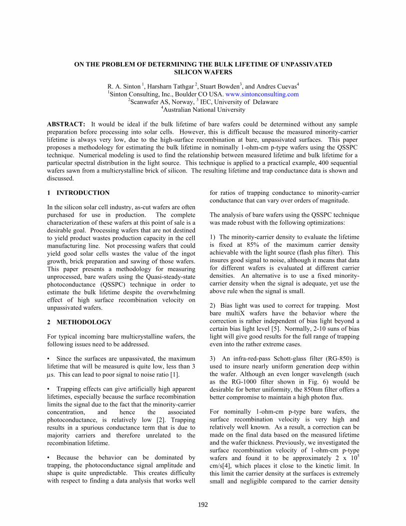
ON THE PROBLEM OF DETERMINING THE BULK LIFETIME OF UNPASSIVATED SILICON WAFERS
R. A. Sinton 1, Harsharn Tathgar 2, Stuart Bowden3, and Andres Cuevas4
1Sinton Consulting, Inc., Boulder CO USA. www.sintonconsulting.com 2Scanwafer AS, Norway, 3 IEC, University of Delaware
4Australian National University
ABSTRACT: It would be ideal if the bulk lifetime of bare wafers could be determined without any sample preparation before processing into solar cells. However, this is difficult because the measured minority-carrier lifetime is always very low, due to the high-surface recombination at bare, unpassivated surfaces. This paper proposes a methodology for estimating the bulk lifetime in nominally 1-ohm-cm p-type wafers using the QSSPC technique. Numerical modeling is used to find the relationship between measured lifetime and bulk lifetime for a particular spectral distribution in the light source. This technique is applied to a practical example, 400 sequential wafers sawn from a multicrystalline brick of silicon. The resulting lifetime and trap conductance data is shown and discussed.
1 INTRODUCTION
In the silicon solar cell industry, as-cut wafers are often purchased for use in production. The complete characterization of these wafers at this point of sale is a desirable goal. Processing wafers that are not destined to yield product wastes production capacity in the cell manufacturing line. Not processing wafers that could yield good solar cells wastes the value of the ingot growth, brick preparation and sawing of those wafers. This paper presents a methodology for measuring unprocessed, bare wafers using the Quasi-steady-state photoconductance (QSSPC) technique in order to estimate the bulk lifetime despite the overwhelming effect of high surface recombination velocity on unpassivated wafers.
2 METHODOLOGY
For typical incoming bare multicrystalline wafers, the following issues need to be addressed.
• Since the surfaces are unpassivated, the maximum lifetime that will be measured is quite low, less than 3 µs. This can lead to poor signal to noise ratio [1].
• Trapping effects can give artificially high apparent lifetimes, especially because the surface recombination limits the signal due to the fact that the minority-carrier concentration, and hence the associated photoconductance, is relatively low [2]. Trapping results in a spurious conductance term that is due to majority carriers and therefore unrelated to the recombination lifetime.
• Because the behavior can be dominated by trapping, the photoconductance signal amplitude and shape is quite unpredictable. This creates difficulty with respect to finding a data analysis that works well
for ratios of trapping conductance to minority-carrier conductance that can vary over orders of magnitude.
The analysis of bare wafers using the QSSPC technique was made robust with the following optimizations:
1) The minority-carrier density to evaluate the lifetime is fixed at 85% of the maximum carrier density achievable with the light source (flash plus filter). This insures good signal to noise, although it means that data for different wafers is evaluated at different carrier densities. An alternative is to use a fixed minority-carrier density when the signal is adequate, yet use the above rule when the signal is small.
2) Bias light was used to correct for trapping. Most bare multiX wafers have the behavior where the correction is rather independent of bias light beyond a certain bias light level [5]. Normally, 2-10 suns of bias light will give good results for the full range of trapping even into the rather extreme cases.
3) An infra-red-pass Schott-glass filter (RG-850) is used to insure nearly uniform generation deep within the wafer. Although an even longer wavelength (such as the RG-1000 filter shown in Fig. 6) would be desirable for better uniformity, the 850nm filter offers a better compromise to maintain a high photon flux.
For nominally 1-ohm-cm p-type bare wafers, the surface recombination velocity is very high and relatively well known. As a result, a correction can be made on the final data based on the measured lifetime and the wafer thickness. Previously, we investigated the surface recombination velocity of 1-ohm-cm p-type wafers and found it to be approximately 2 x 105 cm/s[4], which places it close to the kinetic limit. In this limit the carrier density at the surfaces is extremely small and negligible compared to the carrier density
192

within the wafer. This assumption of high surface recombination velocity can be checked at any time by performing a lifetime measurement with visible light[5].
For perfectly uniform photogeneration and infinite surface recombination velocity it is possible to derive analytically the following relationship between the actual bulk lifetime and the measured effective lifetime [3]:
−= )
2tanh(21
LW
WL
eff ττ Eq. 1
where τ is the bulk lifetime, L is the diffusion length, and W is the wafer thickness.
The Sinton Consulting instruments use a Xenon flash with Schott glass filters. The spectrum for the flash has been measured at NREL, and the filter specifications are known. The PC1D simulation program[6] has been used to determine a relationship analogous to equation Eq. 1 for the practical application using infrared light from the xenon lamp and filters[7].
Simulation of measured lifetime with PC1D, RG850
0
5
10
15
20
25
30
0 0.5 1 1.5 2 2.5
Measured lifetime (µs)
Bul
k Li
fetim
e (m
icro
seco
nds)
300 µm
325 µm
350 µm
Fig. 4. The function to convert measured lifetime to bulk lifetime for the Sinton QSSPC measurements with the Schott-glass RG-850 filter.
These numerically-derived results can be fit with an equation that is analogous to the Eq. 1.
−= )
2tanh(21
LW
WLAeff ττ Eq. 2
Where the factor “A” is a function of the Schott filter type and the wafer thickness. For the 850 nm IR-pass filter,
A = 440W2 – 37.5 W + 1.44
Where W is the wafer thickness in cm. This fit is shown for the 300, 325 and 350 micron-thick simulation in Fig. 4. Notice that a measured lifetime of 1.5 µs would correspond to about 7 µs if the wafer were 350 microns thick, but about 13 µs if the wafer were 300 microns thick. This fit is valid only for the limited range shown here. For the full range, the original numerical curve can be used.
Fig. 5 shows an expanded version of Fig. 4. For a 325 micron-thick wafer, a measured lifetime of 0.8 µs corresponds to a bulk lifetime of 2 µs. A measured lifetime of 1.5 µs corresponds to a 9 µs bulk lifetime. For high bulk lifetimes, small uncertainties in the measured lifetime become large uncertainties in the bulk lifetime. As expected, this is especially true for thinner wafers. In the thin limit, the measured lifetime is completely determined by the surface recombination and transport parameters rather than bulk lifetime.
Simulation of measured lifetime with PC1D, RG850
0
1
2
3
4
5
6
7
8
9
10
0 0.5 1 1.5
Measured lifetime (µs)
Bul
k Li
fetim
e (m
icro
seco
nds)
300 µm
325 µm
350 µm
Fig. 5. The PC1D simulations for conversion of measured to bulk lifetime. The diamonds are the PC1D points, the lines are fits using eq. 2.
The conversion of measured to actual lifetime proposed here is different than the recent paper than we presented in Osaka. In that paper, we proposed that for uniform generation, the correction would be[4]:
11
1bulk
−−− −= sQSSPCmeasusredQSSPC τττ
that might be taken to imply that
21
1
bulk 12W
DnQSSPCmeasusredQSSPC −= −− ττ
which is incorrect for the QSSPC case, except when the diffusion length is extremely high. This became clear in the numerical simulations for this work, and has been verified using the analytical equations as
193

well[3,7]. Unlike the transient case for steady-state measurements(8), the surface recombination lifetime term is a function of the bulk lifetime. In the low-lifetime regime, with L<W, the above QSSPC equation would result in a 15% error in the calculated bulk lifetime.
The curves shown in Fig. 4 and 5 were calculated numerically for the photon distribution particular to the Schott-glass 850 nm IR pass filter, as shown in Fig. 6.
0
1
2
3
4
5
6
7
200 400 600 800 1000 1200Wavelength (nm)
Phot
ons
- nm
-1 (A
.U.)
α =1 µm
α = 42 µm
α = 160 µm
α =14µm
Fig. 6, the photon distribution from a Quantum flash through 3 Schott-glass filters, the BG-38, RG-850, and RG-1000.
3. PRACTICAL APPLICATION:
An application of this lifetime testing methodology is shown in Fig. 7, where the measured lifetime, resistivity, and trap conductance are shown for 400 sequentially-measured wafers in the original order in which they were grown in the brick. These wafers have no surface passivation.
0
0.2
0.4
0.6
0.8
1
1.2
1.4
1.6
1.8
2
0 100 200 300 400
Wafer # from bottom of Brick
lifet
ime
( µs)
and
ohm
-cm
0
1E+14
2E+14
3E+14
4E+14
wafers from block 25
trap
con
duct
ance
(A.U
.)
Ohm-cm
Lifetime
Traps
Fig. 7. The measured lifetime for 400 sequential wafers from a corner brick from a multicrystalline ingot. The measured resistivity and trapping conductance is also shown.
The measured lifetime is surprising smooth, with little random noise apparent in the measurement. The lifetime from wafer 1 at the bottom of the brick to wafer 400 at the top shows the trends expected based on typical block measurements, with the low lifetimes at both ends, and the highest lifetime in the middle of the brick on the side towards the bottom of the brick[9].
Although the minority-carrier photoconductance is capped to be less than 2 µs by the overwhelming effect of the surface recombination velocity on the measured lifetime, the trapping photoconductance (a majority carrier effect) should be the same on passivated or unpassivated wafers. Therefore, it should be very interesting to search for clues in this trapping data that correlate to cell performance. Accurate tracking of trapping in wafers should not require surface passivation.
0
2
4
6
8
10
12
14
16
18
20
0 100 200 300 400
Wafer # from bottom of Brick
lifet
ime
( µs)
0
1E+14
2E+14
3E+14
4E+14
wafers from block 25
trap
con
duct
ance
(A.U
.)
Lifetime
Traps
Corrected for S
Fig. 8 The estimated bulk lifetime based on the data from Fig. 7., 325-µm nominal wafer thickness and equation 2.
Figure 8 shows the bulk lifetime for these 400 wafers as calculated from eq. 2. This procedure essentially removes the 2-µs ceiling imposed by surface recombination in Fig. 7, indicating that the bulk lifetime in parts of this block was greater than 15 µs.. These lifetimes should correspond to a calibrated measurement done on the block, or to measurements done on these same wafers with surface passivation. This further experiment was not performed on these wafers at this time.
From Fig. 4 and 5, it is clear that for calculated bulk lifetimes greater than 10 µs, small uncertainties in the measured lifetime translate to large uncertainties in the bulk lifetime. In practice, these errors could be minimized by measuring the thickness of each wafer instead of using a nominal thickness. The use of
194
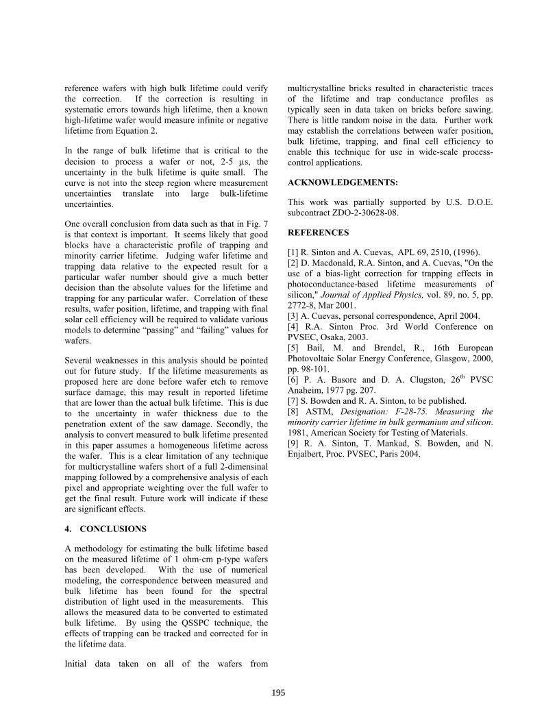
reference wafers with high bulk lifetime could verify the correction. If the correction is resulting in systematic errors towards high lifetime, then a known high-lifetime wafer would measure infinite or negative lifetime from Equation 2.
In the range of bulk lifetime that is critical to the decision to process a wafer or not, 2-5 µs, the uncertainty in the bulk lifetime is quite small. The curve is not into the steep region where measurement uncertainties translate into large bulk-lifetime uncertainties.
One overall conclusion from data such as that in Fig. 7 is that context is important. It seems likely that good blocks have a characteristic profile of trapping and minority carrier lifetime. Judging wafer lifetime and trapping data relative to the expected result for a particular wafer number should give a much better decision than the absolute values for the lifetime and trapping for any particular wafer. Correlation of these results, wafer position, lifetime, and trapping with final solar cell efficiency will be required to validate various models to determine “passing” and “failing” values for wafers.
Several weaknesses in this analysis should be pointed out for future study. If the lifetime measurements as proposed here are done before wafer etch to remove surface damage, this may result in reported lifetime that are lower than the actual bulk lifetime. This is due to the uncertainty in wafer thickness due to the penetration extent of the saw damage. Secondly, the analysis to convert measured to bulk lifetime presented in this paper assumes a homogeneous lifetime across the wafer. This is a clear limitation of any technique for multicrystalline wafers short of a full 2-dimensinal mapping followed by a comprehensive analysis of each pixel and appropriate weighting over the full wafer to get the final result. Future work will indicate if these are significant effects.
4. CONCLUSIONS
A methodology for estimating the bulk lifetime based on the measured lifetime of 1 ohm-cm p-type wafers has been developed. With the use of numerical modeling, the correspondence between measured and bulk lifetime has been found for the spectral distribution of light used in the measurements. This allows the measured data to be converted to estimated bulk lifetime. By using the QSSPC technique, the effects of trapping can be tracked and corrected for in the lifetime data.
Initial data taken on all of the wafers from
multicrystalline bricks resulted in characteristic traces of the lifetime and trap conductance profiles as typically seen in data taken on bricks before sawing. There is little random noise in the data. Further work may establish the correlations between wafer position, bulk lifetime, trapping, and final cell efficiency to enable this technique for use in wide-scale process-control applications.
ACKNOWLEDGEMENTS:
This work was partially supported by U.S. D.O.E. subcontract ZDO-2-30628-08.
REFERENCES
[1] R. Sinton and A. Cuevas, APL 69, 2510, (1996). [2] D. Macdonald, R.A. Sinton, and A. Cuevas, "On the use of a bias-light correction for trapping effects in photoconductance-based lifetime measurements of silicon," Journal of Applied Physics, vol. 89, no. 5, pp. 2772-8, Mar 2001. [3] A. Cuevas, personal correspondence, April 2004. [4] R.A. Sinton Proc. 3rd World Conference on PVSEC, Osaka, 2003. [5] Bail, M. and Brendel, R., 16th European Photovoltaic Solar Energy Conference, Glasgow, 2000, pp. 98-101. [6] P. A. Basore and D. A. Clugston, 26th PVSC Anaheim, 1977 pg. 207. [7] S. Bowden and R. A. Sinton, to be published. [8] ASTM, Designation: F-28-75. Measuring the minority carrier lifetime in bulk germanium and silicon. 1981, American Society for Testing of Materials. [9] R. A. Sinton, T. Mankad, S. Bowden, and N. Enjalbert, Proc. PVSEC, Paris 2004.
195
Spatial Variation of Oxygen and Carbon Precipitation in Polycrystalline Sheet Silicon
Jinggang Lu1, a) and George Rozgonyi1, James Rand2, and Ralf Jonczyk2
Materials Science and Engineering Department, North Carolina State University, Raleigh, NC27695-7916 GE Energy., Solar Park, Newark, Delaware 19711
a) Email: [email protected]
Abstract The spatial variation of oxygen and carbon precipitation across the thickness of polycrystalline sheet silicon has
been investigated by Fourier transform infrared (FTIR) microspectroscopy and preferential etching/optical microscopy. FTIR shows that interstitial oxygen is depleted near the top surface of the as-grown sample; whereas carbon is homogeneously distributed across the wafer thickness. Both oxygen and carbon precipitation were suppressed near the top surface during subsequent annealing, and a 250µm wide precipitate denuded zone was generated, which was also revealed by preferential etching and electron beam induced current imaging preformed on polished cross-sections. Evidently, growth induced near-surface reduction of the oxygen profile keeps the oxygen supersaturation below a critical level for precipitate nucleation. Considering that the minority carrier diffusion length of current finished sheet silicon solar cells ranges from 50 to 100µm, it is anticipated that optimization of the 250µm wide precipitate denuded zone will improve solar cell performance.
I. Introduction The direct growth of sheet or ribbon silicon from molten Si has received increased attention in recent years
because it is highly suitable for low-cost terrestrial-based solar cells1. The Silicon-Film sheets studied here are grown in a horizontal configuration. This permits a two orders higher pulling rate than the vertical configuration used in EFG and string ribbon technologies by decoupling the pulling direction from that of grain growth2. Since each grain only needs to grow a distance equal to the sheet thickness, low-cost, impure feedstock can be used without deteriorating the grain structure integrity. Accompanying these cost-efficiency advantages, the impurity concentration is usually high due to the relative large contact area with the substrate and the low cost silicon feedstock used in sheet generation3, 4. Thus, detailed knowledge is required on the impact of impurities on cell performance to take advantage of this highly cost-effective growth process. Of particular importance is the control of oxygen and carbon precipitation, which can significantly degrade the minority carrier lifetime. Because the low-cost feedstock usually contains a high content of oxide, the concentration of interstitial oxygen (Oi) in the as-grown wafers usually reaches 1018 cm-3. Once incorporated into the wafer, precipitation of supersaturated Oi is enhanced during annealing because of the presence of readily available impurity and microdefect nucleation centers. Studies of carbon in Czochralski silicon have mainly focused on its enhancement effect on oxygen precipitation5-9 and interactions with silicon self-interstitials (ISi)10, 11. Carbon precipitation by itself is rarely an important process because of the typically low CS levels in silicon wafers. The situation is very different in polycrystalline ribbon silicon, which usually contains a high concentration of CS, ranging from 4 to 6 x 1017 cm-3. The high degree of carbon supersaturation and the presence of interstitial oxygen (Oi) enhance the formation of carbon precipitates. The characterization presented in this paper reveals a 250µm wide precipitate denuded zone near the top surface generated through combined control of the growth and annealing processes. Thus, the detrimental effect of precipitates on the minority carrier lifetime is partially eliminated.
A denuded zone near the top surface is usually considered not to be useful for silicon solar cells since the entire wafer thickness is functioning as an active region with respect to light absorption and minority carrier collection. While this is absolutely true for high efficiency solar cells, it is not true for solar cells made from low-cost silicon sheets. Because the minority carrier diffusion length of the sheet silicon is about 50 to 100µm, a high lifetime denuded zone with a width of 250µm will certainly improve the cell performance. Denuded zone formation coupled with internal gettering has been successfully employed in the integrated circuit industry for device yield improvement in the past three decades12, 13. Such a traditional denuded zone is usually achieved through a three step, high-low-high annealing process, and its width is in general below 20µm, which is too small for significant solar cell efficiency improvement. A 250µm OP denuded zone in sheet silicon is achieved through a combined control of the growth and annealing processes. First, a large Oi denuded zone is installed into the silicon sheet by enhancing SiO evaporation via a more aggressive growth thermal profile. The Oi denuded zone is further sustained as a precipitate denuded zone during the following annealing. II. Experiments
Polycrystalline sheet silicon wafers used in this study were generated at a linear sheet speed of 3.1 meters/min
196

at GE Energy (formerly Astropower Inc). A more aggressive growth thermal profile was used to facilitate oxide dissolution and SiO evaporation. The upper region of the polycrystalline silicon sheet has columnar grains, ranging in size from 200 µm to 2 mm. One inch square samples cut from an eight inch wide silicon sheet were annealed in air at 900 and 12000C for 4h, and at 10500C for 2, 4, 8, and 16 h, respectively, to study oxygen and carbon precipitation in sheet silicon.
The Oi depth profiles were characterized by cross-sectional Fourier transform infrared (FTIR) microspectroscopy at 4.2K using a Digilab FTS-6000 spectrometer equipped with an UMA 500 infrared microscope and a continuous liquid-He cooled micro-cryostat from Oxford Instruments. Low temperature measurements are required to measure Oi concentration in annealed samples, due to the need for separating the Oi peak from the OP bands14. A 1.5 mm wide strip was cut from each sample and double-side cross-sectionally polished to 300µm. A thin sample is required to minimize the infrared beam spreading inside the sample, and to prevent the Oi absorption from saturation at low temperatures. FTIR microspectroscopy was performed on the polished cross-section with a step size of 50 µm and an aperture size of 250 x 40 µm2. The long edge parallel to the wafer surface increased the beam intensity, while the short edge perpendicular to the wafer surface increased the spatial resolution. The spectral resolution was set at 4 cm-1 to eliminate interference fringes due to multiple-internal reflections. Since the narrow-band MCT detector of the UMA 500 IR microscope cuts off at ~650 cm-1, the depth profile of Cs, which gives rise to a signature absorption at 607cm-1, could not be resolved. Therefore, Cs profiles were further characterized on a Bruker 66v/S FTIR spectrometer with an IR microscope\ equipped with a B-doped Si detector working at liquid-He temperature, at the U2A beamline of the National Synchrotron Light Source of the Brookhaven National Laboratory. The distributions of precipitates and associated extended defects were examined by Nomarski optical microscopy following cross-sectional polishing and a 30 sec preferential Secco etching. To verify the impact of precipitates on minority carrier lifetime, Al-Schottky diodes were fabricated on polished cross-sections for electron beam induced current (EBIC) measurements, which were performed on a scanning electron microscope at room temperature with an accelerating voltage of 20 KV and a probe current of ~0.1 nA.
III. Results and Discussion
Figures. 1(a) and (b) are the cross-sectional FTIR spectra of the as-grown and the 10500C, 2h annealed samples. The absorption bands at 850-1050 cm-1 are due to oxynitride particles15. Note that the noise level of the spectra is quite high because of the attenuation of the infrared beam by the small aperture and the two ZnSe windows of the cryostat. The thin samples used in this study also increase the background noise level. However, the Oi absorption peak is still well resolved because of peak sharpening with decreasing temperature. Note that the intensity of the 1136 cm-1 oxygen peak in the as-grown sample decreases towards the top surface, while the oxide absorption band at 1100 cm-1 appears in the deeper region of the sample, see Fig. 1(a). From the fact that the Oi denuded zone does not form in wafers grown with a less aggressive thermal profile, it is proposed that the SiO evaporation from the Si melt during sheet growth is responsible for the denuded zone formation. After 2 hours annealing at 10500C, Oi is still present in the near top surface region, while almost all the interstitial oxygen precipitated in the deeper region, see Fig. 1 (b). Note that the oxide absorption band in the deeper region increased significantly with the Oi precipitation.
The Oi concentration was further calculated from the integrated intensity of the 1136 cm-1 absorption peak, using a conversion factor obtained by measuring Oi concentration of an as-grown, precipitate-free Czochralski wafer at room temperature, and the integrated absorption of the 1136 cm-1 peak of the same sample at 4.2K. Figures 2 (a) and (b) plot the Oi and Cs depth profiles of the as-grown and annealed samples. Note that almost all supersaturated oxygen in the deeper region precipitated during a 4h annealing at 900 and 10500C, while a considerable amount of Oi remained near the top surface region. When annealed at 10200C, the Oi concentration decreased to ~4x 1017 cm-3, corresponding to its solubility level. It is well known that the initial Oi supersaturation ratio has a strong impact on oxygen precipitation in CZ wafers16. When the initial Oi concentration is lower than a critical level for precipitate nucleation, precipitation will be suppressed. On the other hand, the nucleation rate will be high if the initial Oi concentration is high, which further results in rapid precipitation. As a result, more Oi is left in the region having a lower initial Oi concentration.
The opposite volume change associated with oxygen (+) and carbon (-) precipitation favors co-precipitation in an approximate ratio of 2:1, as observed in Czochralski silicon6. It is evident from Figs. 2 (a) and (b) that the carbon reduction is well correlated with oxygen precipitation. Note that in the deeper region of our samples, the measured ratio of oxygen and carbon precipitation is approximately 3:1. The critical step for Cs reduction is the formation of high diffusivity, interstitial carbon (Ci) through a capture of silicon self-interstitial (ISi) generated during oxygen precipitation by Cs atoms. This is the reason why carbon precipitation only occurs in regions with an aggressive oxygen precipitation. These Ci can either form complexes with Oi, co-precipitate with oxygen, or form distinct SiC precipitates.
197

The distributions of oxygen precipitates and associated extended defects were also examined by Nomarski optical microscopy following cross-sectional polishing and a 30 seconds preferential Secco etching. No significant difference was detected between the samples annealed at 900 and 10500C. Figure 3 shows the Nomarski images of the 10500C, 8h annealed sample. Note that a 250µm wide, well-defined precipitate denuded zone was formed near the top surface, see Fig. 3 (a). Under higher magnification, it is evident that the defects in the deeper region are either isolated precipitates or stacking faults (SFs), see Fig. 3 (b). While the generation of ISi during oxygen precipitation makes SF formation thermodynamically favorable, precipitates themselves make SF formation kinetically possible by acting as heterogeneous nucleation sites. Note that ISi generated during oxygen precipitation are consumed in two processes, namely, trapping by Cs and the enhancement of carbon precipitation, and the condensation into SFs.
There are three main limitation factors on diffusion length in the polycrystalline sheet Si; namely, a high density of precipitates, the presence of grain boundaries, and included particles with associated dislocation clusters. Because of the low spatial resolutions of diffusion length characterization techniques (below 100 microns in general), it is difficult to isolate the contribution due to oxygen precipitates from those of grain boundaries and dislocation clusters. As a result, we cannot say the diffusion length is improved/degraded because of the denuded zone, even if the measured diffusion length is indeed higher/lower than that in a control wafer. However, the higher spatial resolution of EBIC permits us to study the impact of precipitates on diffusion length without the interference of grain boundaries and dislocation clusters, although we cannot quantitatively determine the diffusion length from the EBIC contrast. Figure 4 shows the cross sectional EBIC images of the as-grown and annealed samples. Again, the denuded zone was observed in all samples annealed at 900 and 10500C, but not in the as-grown one. Note that a bright contrast with a depth of 200-300µm is formed near the top surface of the annealed samples. Correlated with the FTIR and etching results, the bright contrast near the top-surface region is clearly due to the absence of precipitates. The high density of precipitates in the deeper region might function as beneficial gettering sites for transition metals, further improving the lifetime of the denuded zone. Because precipitates will act as effective recombination sites after decorated by transition metals, and the Fe concentration in the sheet silicon is quite high4, the dark EBIC contrast in the deeper region is clearly due to the high density, decorated precipitates and SFs.
IV. Conclusion In summary, an Oi denuded zone is installed in the as-grown sheet silicon wafer by employing a more
aggressive growth thermal profile. The Oi denuded zone is sustained as a 250 µm wide precipitate denuded zone after annealing. It is also found that the Cs precipitation profile is well correlated with oxygen precipitation. EBIC characterization shows that the lifetime in the denuded zone is significantly improved. Considering that the minority carrier diffusion length of current finished solar cells with no denuded zone is around 50-100µm, it is anticipated that a 250 µm thick denuded zone with an increased minority carrier diffusion length will improve solar cell performance.
The authors would like to thank Dr. Zhenxian Liu of NSLS for his help with FTIR measurements.
Reference 1. J. P. Kalejs, Solar Energy Mater. & Solar Cells, 72, 139 (2002). 2. J. Culik, I. Goncharovsky, J. Rand, and A. Barnett, Prog. in Photovoltaics, 10 (2), 119 (2002). 3. J. Lu, M. Wagener, G. Rozgonyi, J. Rand, and R. Jonczyk, J. Appl. Phys. 94, 140 (2003). 4. A. Istratova, T. Buonassisi, R. McDonald, A. Smith, R. Schindler, J. Rand, J. Kalejs, and E. Weber, J. Appl.
Phys. 94, 6552 (2003). 5. F. Shimura, J. Appl. Phys. 59, 3251 (1986). 6. Q. Sun, K. H. Yao, J. Lagowski, and H. C. Gatos, J. Appl. Phys. 67, 4313 (1990). 7. S. Hahn, M. Arst, K. N. Ritz, S. Shatas, H. J. Stein, Z. U. Rek, and W. A. Tiller, J. Appl. Phys. 64, 849 (1988). 8. P. Liu, X. Ma, J. Zhang, L. Li, and D. Que, J. Appl. Phys. 87, 3669 (2000). 9. J.-Y. Huh, U. Giisele, and T. Y. Tan, J. Appl. Phys. 78, 5926 (1995). 10. M. S. Carroll, C.-L. Chang, J. C. Sturm, and T. Buyuklimanli, Appl. Phys. Lett. 73, 3695 (1998). 11. P. A. Stolk, D. J. Eaglesham, H.-J. Gossmann, and J. M. Poate, Appl. Phys. Lett. 66, 1370 (1995). 12. T. Y. Tan, E. Gardner, and W. Tice, Appl. Phys. Lett. 30, 175 (1977). 13. A. Borghesi, B. Pivac, A. Sassella and A. Stella, J. Appl. Phys. 77, 4169 (1995). 14. A. Sassella, A. Borghesi, B. Pivac, and M. Porrini, Appl. Phys. Lett. 79, 4106 (2001). 15. J. Lu, G.A. Rozgonyi, J. Rand, and R. Jonczyk, “secondary phase particles in polycrystalline sheet silicon”, J.
Crystal Growth (in press). 16. Annual Book of ASTM Standards, Philadelphia, PA, 1994, Vol. 10.05, p. F1239.
198

Fig. 1. FTIR spectra acquired at 4.2K on the polished cross-sections of (a) as-grown and (b)10500C, 2h annealed sheet silicon samples.
Fig. 2. Depth profiles of Oi (a) and Cs (b) in the as-grown and annealed samples.
Fig. 3. Cross-sectional Nomarski images of the 10500C, 8h annealed sample after 30s Secco etching. (a) low magnification image with top surface facing upwards; (b) zoom in of the shadowed region indicated in (a).
Fig. 4. Cross sectional EBIC images of the as-grown (a), 9000C-4h (b), and 10500C-4h (c) annealed samples. The top surfaces are facing upwards.
(a) (b)
(a)
(b)
(c)
199

HIGH PRODUCTIVITY IN-LINE SCREEN PRINTING SYSTEM FOR CRYSTALLINE SOLAR CELL MANUFACTURING
Julio A. Bragagnolo and Michael Culik
NPC America Corporation, Newark, DE 19711, U.S.A. Masafumi Ito, Hisashi Sato, Junichi Akita, Toru Hashimoto, and Yoshiro Chikaki
NPC Incorporated, Tokyo, Japan.
INTRODUCTION To develop a high performance screen-printing system, the NPC Group defined an appropriate benchmark for characterizing the industrial efficiency of the operation and carried out a full analysis of the factors affecting this benchmark. The chosen benchmark is Cost of Ownership (CoO), origi-nally developed by Sematech for the semiconductor industry (SEMI Standard E-35: Cost of Owner-ship for Semiconductor Manufacturing Equipment). CoO can be calculated from fixed costs FC, re-curring costs RC, yield cost YC, equipment life L, throughput T, yield Y and uptime U:
L.T.Y.U
YC RC FC CoO
++=
Key data in solar cell screen-printing, not usually reported in the open literature under real produc-tion conditions, are the effective throughput Teff=T.Y.U and the yield Y, which affects both Teff and YC. In this paper, we describe the screen-printing system built and report system performance for a large number of cells. Both the machine design as well as the CoO data presented are relevant to the needs of solar cell manufacturers to assess the industrial performance of major cell manufacturing tools in production.
SCREEN PRINTING SYSTEM DESIGN The NPC screen-printing system FasPrinter 200-A has innovative design features directed to mini-mizing CoO. The NPC design minimizes breakage yield losses by minimizing the number of wafer handling steps and using a belt transport that reduces cell edge gripping to a minimum. To minimize breakage further, the system features camera alignment instead of mechanical alignment. To provide increased U, and therefore Teff, the design includes optional solar cell buffers; the choice of buffer location depends on the printing process sequence and the type of thick film ink used. The straight-line system configuration allows for easy operator access and fast maintenance, also con-tributing to high uptime. The FasPrinter 200-A (Figure 1) is designed to print standard thick film inks on 100 mm to 150 mm square or pseudo square crystalline silicon solar cells. The cycle time is 3 seconds per cell, equiva-lent to a raw throughput of 1,200 cells per hour. The FasPrinter 200-A for standard thick film inks features short, integrated dryers using hot air and infrared heat. This reduces the fixed cost FC by reducing the total footprint to approximately 20 m2.
200
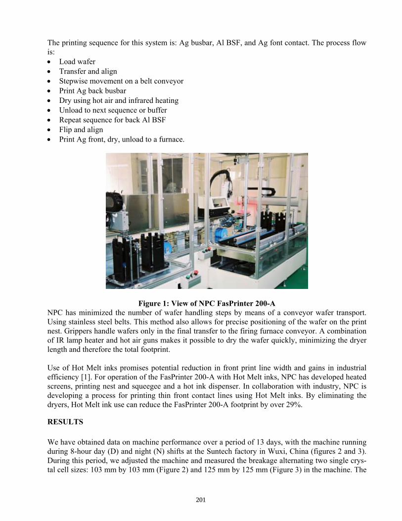
The printing sequence for this system is: Ag busbar, Al BSF, and Ag font contact. The process flow is: • Load wafer • Transfer and align • Stepwise movement on a belt conveyor • Print Ag back busbar • Dry using hot air and infrared heating • Unload to next sequence or buffer • Repeat sequence for back Al BSF • Flip and align • Print Ag front, dry, unload to a furnace.
Figure 1: View of NPC FasPrinter 200-A NPC has minimized the number of wafer handling steps by means of a conveyor wafer transport. Using stainless steel belts. This method also allows for precise positioning of the wafer on the print nest. Grippers handle wafers only in the final transfer to the firing furnace conveyor. A combination of IR lamp heater and hot air guns makes it possible to dry the wafer quickly, minimizing the dryer length and therefore the total footprint. Use of Hot Melt inks promises potential reduction in front print line width and gains in industrial efficiency [1]. For operation of the FasPrinter 200-A with Hot Melt inks, NPC has developed heated screens, printing nest and squeegee and a hot ink dispenser. In collaboration with industry, NPC is developing a process for printing thin front contact lines using Hot Melt inks. By eliminating the dryers, Hot Melt ink use can reduce the FasPrinter 200-A footprint by over 29%.
RESULTS We have obtained data on machine performance over a period of 13 days, with the machine running during 8-hour day (D) and night (N) shifts at the Suntech factory in Wuxi, China (figures 2 and 3). During this period, we adjusted the machine and measured the breakage alternating two single crys-tal cell sizes: 103 mm by 103 mm (Figure 2) and 125 mm by 125 mm (Figure 3) in the machine. The
201

data shows that cell handling meets the breakage target of well below 1% demonstrated in other NPC machines [2].
0
2000
4000
6000
8000
10000
12000
1 N 2 D 2 N 3 D 3 N 4 D 4 N 5 D 5 N 6 D 6 N 10 D 10 N 11 D 11 N
Production Day and Shift
Num
ber P
roce
ssed
0.00%
0.20%
0.40%
0.60%
0.80%
1.00%
1.20%
1.40%
1.60%
1.80%
2.00%
Bre
akag
eLeft Scale
Right Scale
Figure 2: Manufacturing breakage for 143,247 crystalline silicon cells, 103 mm in size, made in 15 day (D) and night (N) shifts during 13 production days.
0
2000
4000
6000
8000
10000
12000
7 D 7 N 8 D 8 N 9 D 9 N 12 N 13 D 13 N
Production Day & Shift
Num
ber o
f Cel
ls P
roce
ssed
0.00%
0.50%
1.00%
1.50%
2.00%
Bre
akag
e
Left Scale
Right Scale
Figure 3: Manufacturing breakage for 74,468 crystalline silicon cells, 125 mm in size, made in 9 day (D) and night (N) shifts during 13 production days.
202

The average breakage for the complete three-print metallization process is 0.7% for 125 mm cells and 0.4% for 103 mm cells. Some fluctuation was observed in the cell breakage after changing cell sizes and occasionally during night shifts; however, the breakage rate stayed below 1%. In addition, we have measured the actual throughput as the ratio of the actual number of printed wa-fers to the total expected number, over 12 hour running periods in 4 production days. The 4-day data shows actual throughputs between 83 and 94% with an 88% average for 125 mm single crystal wa-fers. We have completed a preliminary CoO calculation based on the data available from the test and ad-justment task at Suntech. As is well known, the thick film ink cost is the dominant factor which de-termining CoO for this process. Therefore, it is appropriate to analyze the contribution to the costs that can be attributed to the printing tool. The costs attributable to the FasPrinter 200-A are mainly: equipment depreciation, labor (both operating and maintenance), which is influenced by local labor costs, and scrap. We obtain equipment costs and scrap costs of below 4% and 2% respectively; the sum of both is always below about 6% of the total CoO. As we are able to refine the actual costs of the various inputs, we plan to publish a detailed CoO with absolute values.
CONCLUSIONS A screen-printing system design based on careful cost analysis can produce a machine with a high effective throughput and low cell breakage. As a result, NPC can now offer advanced, in-line, high throughput precision systems to the Photovoltaics Industry.
REFERENCES [1] Todd Williams et al., “Hot Melt Ink Technology for Crystalline Silicon Solar Cells”, 29th IEEE PVSC Proceedings, p.352, 2002. [2] Julio A. Bragagnolo et al., “Processing of Crystalline Silicon Solar Cells in High Throughput Production Tools”, 29th IEEE PVSC Proceedings, p.383, 2002.
ACKNOWLEDGEMENTS We gratefully acknowledge the collaboration of Zhengrong Shi, Managing Director of Suntech Power in allowing us to use the data. We are indebted to Alan Levine of Wright Williams & Kelly for his assistance with CoO analysis.
203

Stress-Induced Nitrogen and Oxygen Segregation and Complexing Investigated by High Resolution Synchrotron FTIR
A. Karoui1, T. Buonassisi,2 F. Sahtout Karoui, 1 G. A. Rozgonyi,1
M. Michael,3 E. R. Weber,2 T. Ciszek4
1. Dept. of Materials Science & Eng., North Carolina State University, NC 2. Dept. of Materials Science & Eng., University of California at Berkeley, CA
3: ALS, Lawrence Berkeley National Laboratory, CA 4: National Renewable Energy Laboratory, CO
Abstract: Nitrogen doped Czochralski (N-CZ) and Float Zone (N-FZ) silicon were measured by high resolution synchrotron Fourier Transform IR spectroscopy (HR-FTIR). The chemical complexes were analyzed in specific regions with known extended defects, i.e., denuded or precipitated regions of annealed N-CZ Si wafers, in N-FZ Si with ring defects and on “N-Skin” region. The absorption lines were assigned to chemical complexes previously studied by first principles calculations. In annealed N-CZ Si wafers, a strong correlation was observed between the absorption line intensity depth variations and the defect distributions revealed by an Oxygen Precipitate Profiler (OPP), and oxygen and nitrogen SIMS profiles. Transformation of chemical complexes from one type to another was observed. A defect band, visible as an OPP peak at the denuded zone-bulk interface was found to be related to vacancy defect enhancement of oxygen precipitation via production of mobile N2. For the as grown N-FZ, the radial dependency of IR absorption line intensity is correlated to x-ray topography contrast.
I. Introduction
The large number of predicted IR absorption lines in N CZ silicon and the variations in experimental conditions (thermal history) complicate the assignment of these lines to chemical complexes. However, high spatial resolution Fourier Transform Infra-Red spectroscopy (HR-FTIR), supported by quantum mechanics calculations, is a powerful mean for analyzing complexes in special regions. In N-doped silicon we have investigated unique N and O related extended defects by various techniques including OPP/etching, HRTEM, Z-contrast and EELS, SIMS simultaneous profiling [1, 2] to depict the mechanisms of defect formation. The robustness of our complex identification method stems from detailed data on these extended defects and absorption line predictions by atomistic calculations. We also verify the viability of the identified N-O-V species (in as grown and annealed silicon) to their formation and stability thermodynamics. These interrelated studies on complexes benefit the continuum clustering modeling of extended defect growth in silicon [3, 4, 5].
The objective of this work is to use HR-FTIR depth profiling spectroscopy to detect chemical complexes produced in subsurface of annealed N-doped Czochralski (N-CZ) wafers [6, 7, 8]. To consolidate this analysis, a N-doped Float Zone (N-FZ) Si wafer is examined along its radius, where N defects vary. Assignment of detected IR optical lines, to previously proposed operative chemical complexes, relies on previously published results from first principles calculations. Among other N related issues, this study addresses the mechanisms of N and O co-segregation.
II. Experimental Methods
A state-of-the-art optical bench at the ALS [9] was used. It consists of a Nicholet IR microscope that produces a 5 to 10 µm spot size, a LN2-refrigerated detector and an MCT (HgCdTe) He-refrigerated bolometer, and utilizes an IR light beam induced by a bending magnet in a synchrotron ring. The beam is highly collimated and more than 3 orders of magnitude brighter than a Globar source [10]. HR-FTIR line scans are necessary for precisely mapping the distribution of N and O species in N-CZ subsurface defects [1], and in N induced native extended defects (the N-FZ ‘N-Skin’ [11]). Line extraction is made possible by using a background spectrum from a defect free zone of the same sample acquired under identical conditions.
III. Results and discussions
1) N and O segregation in N-CZ heat treated wafers We discuss in this section FTIR data on N-O complex nature and distributions, in N-CZ wafer Lo-Hi annealed at
650°C for 8 Hrs and 1050°C for 16 Hrs. Based on OPP and SIMS depth profiling, we previously reported [1] that three regions were identified [12]; Fig. 1(a) shows a typical OPP profile. The first region spreads over 2µm and is saturated with N and O. Due to thermal stresses, up to 1x1018 cm-3 out-diffused nitrogen and 2x1021cm-3 oxygen accumulated at the subsurface, which results in ultra shallow subsurface oxynitride layer. The latter is interesting for photovoltaic and optoelectronic devices [13, 14] but intriguing for IC technologies, because it contains a large density of small equilibrium precipitates [2]. The second region, referred to as Low Density defect Zone (LDZ), is basically an “oxygen
204

denuded zone” that was strongly modified by N [2] and is left (after annealing) with a low density of very small precipitates and nuclei comparable to the N-CZ as grown defects. The third is characterized by high density of precipitates and SF(s) that are formed by a significantly different mechanism than in N free CZ Si [2].
Figure 1(b) shows a 2D representation of the differential reflectance spectra and Fig. 1(c) the absorbance spectra as a function of depth. The intensity of the some absorbance lines are shown in Fig. 2(a); similar curves that are relevant to OPP profile features (in region III) are provided separately are provided in Fig. 2(b). The table in Fig. 2(c) gives an analysis of the absorption line positions in the three regions of the Lo-Hi beveled sample. These were obtained from the absorbance spectra given in Fig. 1(c). Lines are compared between themselves (within each of the three regions) and assigned to chemical complexes in connection to previously calculated absorption [6].
Depth (µm) 0 10 20 30 40 50 60
II
BM
D D
ensi
ty ( x
109 c
m-3
)
0.05
10
20
30 I III
Edge
III II Region I
4003002001000
1 2 00
10 00
Bevel
6 00
8 00
1086420Depth (µm)
0.05
0.07
0.09
0.11
0.13
0.15
0.17
0.19
0.21
0.23
650 750 850 950 1050 1150Wavenumber (cm-1)
Abs
orba
nce
(a) (b) (c)
Fig. 1: (a) Defect depth distribution by OPP in Lo-Hi cycled wafer. (b) Differential reflectance spectra by HR-FTIR along bevel polished sample (magnification=50). (c) Differential absorbance spectra calculated from measured reflectance.
It is remarkable that in region I all lines show higher intensities and decay in the same fashion. More importantly, the decays have shape and the same depth range as the OPP defect density profile, in that region. Moreover, the shape of 984.1, 666.4, and 837.5 cm-1 and to less extent 681.3, 864.9, and 870.1, 890.1 cm-1 lines reproduce the OPP profile. This is especially visible on the peak at the beginning of region III, while 810.9 and 950.7cm-1 lines show at that depth an opposite behavior to the OPP depth profiles. This data indicates the close relation of the identified complexes to the extended defects (detected by OPP, see Fig. 1(a)), as well as the interrelation between the complexes to which these IR lines belong. This represents a unique evidence of N-O species conversion into V-N. It occurs by loss of O from V-N-O complexes (i.e., reduction of N2O , V2N2O , and V2N2O2 concentrations) while increasing the concentration of V-N complexes (i.e., V2N2 and N2). Note that the reflectance line at 1107 cm-1 (finger print of interstitial oxygen: Oi) varies smoothly, and increases in the subsurface towards the surface.
2) N complexes in as-grown N-FZ
We previously reported that the attempt of doping float zone silicon with high level of nitrogen using N2 atmosphere gas during the zoning, leads to a non uniform distribution of the dopant [14]. As shown in the XRT image of a N-FZ 32 mm diam wafer, see Fig. 3(a), an external layer referred to as nitrogen-skin (N-Skin) is formed. In addition, there is a hallow of high density of pits (left in the central region after a long slurry polishing) that might be originated by voids in the central region, see micrograph in Fig. 3(a). Moreover, the XRT shows a series of co-centric rings (white contrast). The color coded map (see the strip superimposed to the XRT image) shows the correlation of chemical complex IR absorption and structural defects (rings). Because of the nitrogen and oxygen saturation in the ingot rim, the stresses during the FZ Si zoning, and the cooling rate, we expect a variety of N-V species. Therefore the “N-Skin” wafer is an excellent test-bed for delineating N-V complexes with HR-FTIR.
Figure 3(b) shows the differential absorbance spectra along the radius, excluding the central defected zone. In the differentiation we used the spectrum acquired 6mm away from the wafer center as reference. One must first note that the Oi line (1106 cm-1) is not detected. Secondly, the N related band (between 650 and 720 cm-1) is the most dominant, its intensity increases as we go from the center to the wafer edge and fluctuates at the same spacing as the XRT rings of Fig. 3(a). In fact, this band is formed of four N-related lines, among which three are found in N-CZ (666.4 and 681 cm-1 both assigned to V.
2N2), the third is 696.5 cm-1 (attributed to V2N2O). However, line V2N2 must be dominant. The smaller bands appearing between 720 and 890 cm-1 like in NCZ, see Fig. 2(c), are related to VNO and NO complexes. Although their intensity is limited ,as expected from FZ material, to ¼ of similar ones in N-CZ, they show that N and O inevitably couple in float zone Si. This is in line with the very strong coupling of N and O found in
A
205
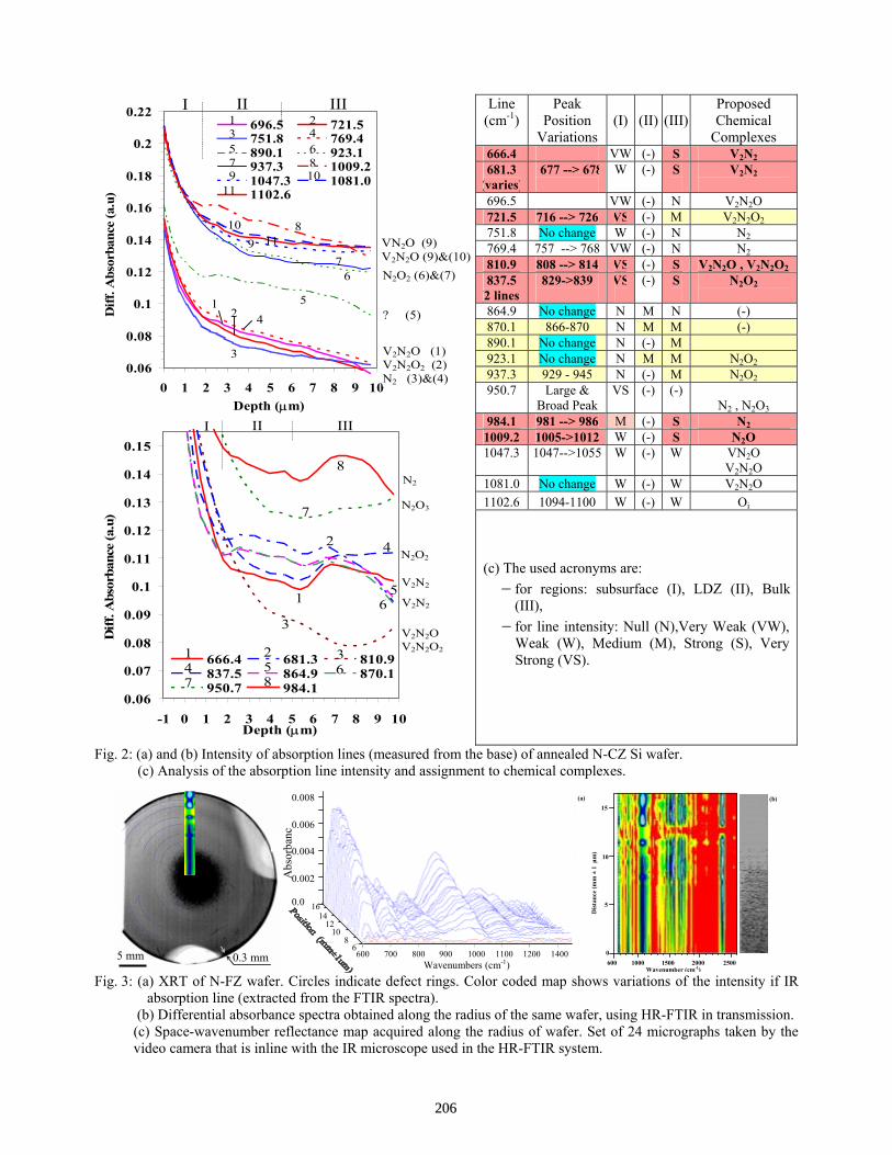
Line (cm-1)
Peak Position
Variations (I)
(II)
(III)
Proposed Chemical
Complexes 666.4 VW (-) S V2N2 681.3
(varies)677 --> 678
W
(-)
S
V2N2
696.5 VW (-) N V2N2O 721.5 716 --> 726 VS (-) M V2N2O2 751.8 No change W (-) N N2 769.4 757 --> 768 VW (-) N N2 810.9 808 --> 814 VS (-) S V2N2O , V2N2O2 837.5
(2 lines)829->839
VS
(-)
S
N2O2
864.9 No change N M N (-) 870.1 866-870 N M M (-) 890.1 No change N (-) M 923.1 No change N M M N2O2 937.3 929 - 945 N (-) M N2O2 950.7
Large &
Broad Peak VS
(-)
(-)
N2 , N2O3 984.1 981 --> 986 M (-) S N2
1009.2 1005->1012 W (-) S N2O 1047.3
1047-->1055
W
(-)
W
VN2O V2N2O
1081.0 No change W (-) W V2N2O 1102.6 1094-1100 W (-) W Oi
0.06
0.08
0.1
0.12
0.14
0.16
0.18
0.2
0.22
0 1 2 3 4 5 6 7 8 9 10Depth (µm)
Diff
. Abs
orba
nce
(a.u
)696.5 721.5751.8 769.4890.1 923.1937.3 1009.21047.3 1081.01102.6
I II III
VN2O (9) V2N2O (9)&(10)N2O2 (6)&(7)
V2N2O (1) V2N2O2 (2) N2 (3)&(4)
? (5)
1 3 5 7 9
11
3
4 1
2 5
6 7
8 10 9 11
2 4 6 8 10
0.06
0.07
0.08
0.09
0.1
0.11
0.12
0.13
0.14
0.15
-1 0 1 2 3 4 5 6 7 8 9 10Depth (µm)
Diff
. Abs
orba
nce
(a.u
)
666.4 681.3 810.9837.5 864.9 870.1950.7 984.1
I II III
V2N2
N2O2
V2N2O V2N2O2
N2
N2O3
V2N2
1 2 3 4 5 6 7 8
1
2
3
4
56
7
8
(c) The used acronyms are: − for regions: subsurface (I), LDZ (II), Bulk
(III), − for line intensity: Null (N),Very Weak (VW),
Weak (W), Medium (M), Strong (S), Very Strong (VS).
Fig. 2: (a) and (b) Intensity of absorption lines (measured from the base) of annealed N-CZ Si wafer. (c) Analysis of the absorption line intensity and assignment to chemical complexes.
5 mm 0.3 mm
Wavenumbers (cm-1)700
8 10 12 14 16
6
Abs
orba
nc
0.0 0.002 0.004 0.006 0.008
800 900 1000 1100 1200600 1400
600 1000 1500 2000 2500 Wavenumber (cm-1)
5
10
15
0
Dis
tanc
e (m
m ±
1 µ
m)
(a) (b)
Fig. 3: (a) XRT of N-FZ wafer. Circles indicate defect rings. Color coded map shows variations of the intensity if IR
absorption line (extracted from the FTIR spectra). (b) Differential absorbance spectra obtained along the radius of the same wafer, using HR-FTIR in transmission. (c) Space-wavenumber reflectance map acquired along the radius of wafer. Set of 24 micrographs taken by the video camera that is inline with the IR microscope used in the HR-FTIR system.
206
N-CZ Si [2]. The N and O interactions were discussed in Ref.2 based on O and N simultaneous profiling with HR-SIMS of the subsurface of N-CZ silicon. The stronger and broader band spreading from 920 to 1100 cm-1 is attributed to oxynitride phases within the silicon matrix. It denotes large variations in the concentrations of V-N species. It is remarkable that the V-N-O lines are detectable in this N-FZ wafer, and that their intensity increases as we go toward the wafer rim, where oxynitride skin is initiated. Moreover, the N appeared strong enough to drag a lot of oxygen and form oxynitride at the peripheral ring of the ingot as well as in the ring regions inside the wafer.
Conclusion
Detailed information relevant to chemical complex generation in N doped silicon were obtained using the HR-FTIR setup at the Advanced Light Source. The differential FTIR spectra (using background spectrum from the same line scan) reveal the smallest possible lines and increases the high resolution capabilities.
Using data from atomistic calculations, reported elsewhere, we have singled out the prominent FTIR lines. A variety of complexes in each of the three Lo-Hi annealed N-CZ wafer regions were identified. A strong correlation of the intensity depth profile of absorption lines with the OPP defect density was found for the three regions, in particular the subsurface region and at the LDZ-bulk interface. The surface effected the nature of these complexes by providing the necessary vacancies to form the most stable complexes at the surface and in the subsurface. In the N doped float zone we could detect the V-N species, as well as, N-O complexes. Acknowledgements: The authors thank Dr D. Yang from Zhejiang University, China, for providing the N doped CZ silicon. This work is supported by the National Renewable Energy Laboratory Grant # AAT-2-31605-05. The FTIR measurements were done at the Advanced Light Source of the LBNL. The Advanced Light Source is supported by the Director, Office of Science, Office of Basic Energy Sciences, Materials Sciences Division, of the U.S. Department of Energy under Contract No. DE-AC03-76SF00098 at Lawrence Berkeley National Laboratory. References 1. A. Karoui, F. Sahtout, G. A. Rozgonyi, and D. Yang, Oxygen Precipitation in Nitrogen Doped Czochralski Silicon
Wafers. Part-I: Formation Mechanisms of Near-Surface and Bulk Defects J. Appl. Phys. , 15 Aug. 2004. 2. A. Karoui, G. A. Rozgonyi, Oxygen Precipitation in Nitrogen Doped Czochralski Silicon Wafers, Part-II :
J. Appl. Phys. , 15 Aug. 2004. 3. F. Sahtout Karoui, A. Karoui, and G. A. Rozgonyi, Simulation of Point Defect Clustering in Cz-Silicon Wafers On
The Cray T3E Scalable Parallel Computer: Application Toto Oxygen Precipitation, MSM2000, San Diego, March 27-29, p. 98, (2000).
4. J. Esfandyari, C. Schmeiser, S. Senkader, G. Hobler, J. Electrochem. Soc. ,143, No3, 995 (1996). 5. M.Schrems, T.Bradec, M. Budil, H. W.Potzl, E. Guerrero, D.Huber, P. Pongratz, Mat. Sc. and Eng. ,B4, 393 (1989). 6. F. Sahtout Karoui, A. Karoui, G. A. Rozgonyi, M. Hourai, and K. Sueoka, Characterization of Nucleation Sites in
Nitrogen Doped Czochralski Silicon by Density Functional Theory and Molecular Mechanics, Solid State Phenomena, Vols. 95-96, p. 99 (2004).
7. A. Karoui, Faouzia Sahtout Karoui, George A Rozgonyi, Molecular Dynamics and First-Principles Calculations of Defect Precursors Formation in N-doped Silicon, MRS Spring Meeting 2004, Symposium Q: Nucleation Phenomena—Mechanisms, Dynamics, and Structure.
8. N. Inoue, D. Funao, I. Ohkubo, A Natsume, F. Sahtout Karoui, A. Karoui, and G. A. Rozgonyi, Analysis of nitrogen reactions in CZ silicon, in Proceedings of the Forum on the Science and Technology of Silicon Materials 2003, Eds. H. Yamada-Kaneta, and K. Sumino, Shonan Village Center, Kanagawa, Japan, Nov. 25-27, 2003, p.242-246. and in DRIP X, 10th International Conference on Defects: Recognition, Imaging and Physics of Semiconductors in Batz-sur-Mer, France, Sep. 29 - Oct. 2, 2003.
9. The Advanced Light Source produces soft x-ray regions from 0.1 nm (far ultraviolet) up to 100 nm, and Vis-IR of at least 100 µm. ALS light is bright and Highly Collimated.
10. Value given for 2 cm-1 spectral window, which is the typical bandwidth of a FTIR spectrometer. 11. A. Karoui, G.A.Rozgonyi, Minority Carrier Lifetime in Nitrogen Doped FZ Si, Quarterly Report (QR2) of NREL-
NCSU Project “Optimization of Silicon Crystal Growth and Wafer Processing for High Efficiency and High Mechanical Yield” Project Number: AAT-2-31605-05, NCSU, June 30, 2002.
12. A. Karoui, F. Sahtout Karoui, A. Kvit, G. A. Rozgonyi, and D. Yang, Appl. Phys. Lett., 80 (12), 2114 (2002). 13. A. Karoui, R. Zhang, G. A. Rozgonyi, and, T. Ciszek, Silicon Crystal Growth and Wafer Processing for High
Efficiency Solar Cells and High Mechanical Yield, NCPV, NREL/CP-520-31057, Lakewood, CO, 14-17 Oct. 2001. 14. A. Karoui, F. Sahtout, and G. A. Rozgonyi, Patent filled -.Sep. 9, 2003.
207
A Phase Diagram of Hot-Wire CVD Epitaxial Si Films on Si(100) Substrates and
Large-grained Polycrystalline Templates
Christine Esber Richardson, Maribeth S. Mason and Harry A Atwater
Thomas J. Watson Laboratory of Applied Physics, California Institute of Technology, Pasadena, CA 91125 USA
Abstract We have investigated the low-temperature (T = 300-475 C) epitaxial growth of thin silicon films by hot-wire chemical vapor deposition on Si(100) substrates and on large-grained polycrystalline template layers formed by selective nucleation and solid phase epitaxy (SNSPE). Using reflection high energy electron diffraction (RHEED), X-ray diffraction (XRD), and transmission electron microscopy (TEM), we have derived a phase diagram for Si epitaxy on Si(100). Wire temperature was set to 1800 C with wire spacing at 3.5 cm for a growth rate of 1 A/s. The total pressure ranged from 20 to 75 mTorr and H2 dilution [R=H2/SiH4] from 0-50. Films ranged from amorphous, to protocrystalline, to polycrystalline, to epitaxial. Twinned epitaxial films were grown to over 1 µm thickness with R=50 and substrate temperature of 300 C. HWCVD epitaxial growth on large-grained templates is one strategy for the fast low-temperature growth of large-grained films with hydrogen-passivated low-angle grain boundaries. By studying epitaxial Si on Si we can help optimize the deposition parameters for high quality films. Previously we have investigated epitaxial thickness as a function of temperature [Fig. 1]. Now we see the effect of hydrogen dilution on the critical epitaxial thickness and texture of the film. At each temperature there is an optimal dilution to reach the thickest epitaxial film [Fig. 2]. We have studied several deposition parameters and offer a slice in phase space of those results by varying pressure, H dilution, and substrate temperature. In addition, we have grown films with both pure silane and 4% silane dilute in helium. The phases seen range from epitaxy to polycrystalline to protocrystalline using RHEED [Fig. 3] and TEM [Fig. 4]. We have also characterized the structure of these films using AFM to look at the surface texture and light trapping advantage; FTIR to look at the H grain boundary and film incorporation; and photoconductive decay to look at the minority carrier lifetimes using a 532 nm laser as the excitation source. All the films roughened with increased thickness. As the films roughen, the surface morphology effectively increases the film thickness through light trapping, increasing the number of carriers generated. The minority carrier lifetimes for films on Si(100) range from 5.7 to 14.8 microseconds. One or more exponential decays were fit to the curves from which the minority carrier
208
lifetimes for each sample under HLI and LLI conditions were derived. The measured minority carrier lifetime is an effective lifetime; because the surface recombination velocity is not known, this effective lifetime is a lower bound on the true minority carrier lifetime in the material. The RCPCD data for a 1.5 µm HWCVD film on Si is typical of that for bulk Si, with the HLI lifetime greater than the LLI lifetime. This is consistent with an epitaxial film on Si(100). In 3.5 µm and 11.5µm thick films on Si(100), the HLI lifetime is lower than the LLI lifetime. Such a decay pattern is indicative of a shallow recombination center. Since the microstructure of these thicker films is mostly polycrystalline, hydrogen-passivated grain boundaries may be responsible. For a 15 µm thick film on Si(100), a single decay is observed, corresponding to the LLI lifetime. In the SNSPE process, nickel nanoparticles are used as nucleation sites for the solid-phase crystallization of phosphorus-doped amorphous silicon on SiO2, producing polycrystalline films with grain sizes on the order of 100 microns. Because the SNSPE templates are only 100 nm thick, the lifetime of the template layer alone cannot be reliably measured by RCPCD at 532 nm. Minority carrier lifetimes for films on SNSPE templates range from 5.9 to 19.3 microseconds. The decay for the 1.5 µm thick film indicates a single lifetime, while the decays for 3.5µm and 11.5µm thick films are characteristic of a deep-level recombination center. This center may arise from the diffusion of residual nickel from the SNSPE templates into the films. The 15 µm thick film on SNSPE templates is also characterized by a single lifetime. The factor of two discrepancy in lifetime values may be due to nonuniformity in the films. Although nickel is a known lifetime killer even in small concentrations, the lifetimes of films on SNSPE templates are comparable to the lifetimes of films on Si(100). Under LLI conditions, the minority carrier lifetimes for films on Si(100) range from 5.7 to 7.5 µs, and the minority carrier lifetimes for films on SNSPE templates range from 5.9 to 19.3 µs [Fig. 5]. Polycrystalline films grown by HWCVD have been used in the fabrication of 1.5 µm-thick thin- film transistors with channel mobilities of 4.7 cm2/V·s on glass substrates. Using the Einstein relation, we can determine that, if the mobilities in our films were comparable, the minority carrier diffusion coefficient would be 0.1175 cm2/s. From this value and the minority carrier lifetime of ~7 µs measured by RCPCD in a 1.5 µm thick film on Si(100), we obtain a value for the minority carrier diffusion length of approximately 9 µm, which is comparable to the thicknesses of the active layers for thin-film photovoltaics (1–30 µm). The minority carrier lifetimes of films on SNSPE templates are comparable, making it possible that the growth of epitaxial films by HWCVD on large-grained SNSPE templates is a viable strategy for the fabrication of thin-film photovoltaics.
209

Figure 1: Phase diagram of HWCVD films grown at 50:1 hydrogen dilution with 4% SiH4 in He.
Figure 2: Silicon to oxygen ratio in the first monolayer of growth as a function of dilution ratio R (H2/SiH4) at temperatures from 571 to 711 K. Pressure is held constant at 75 mTorr of a gas mixture of H2 and 4% SiH4 in He.
Figure 3: Phases seen in RHEED. (a) Epitaxy (b) Epitaxy starting to twin (c) Twinned Epitaxy (d) Mixed twinned epitaxy/polycrystalline (e) Polycrystalline
a b dc e
210

Figure 4: Protocrystalline film (a) TEM diffraction pattern (b) Dark field TEM of film/substrate interface.
Figure 5: (a) LLI and HLI minority carrier lifetimes of HWCVD films on Si(100) as measured by RCPCD. The dashed and dotted lines represent the LLI and HLI lifetimes, respectively, of the bulk Si(100) substrate. (b) LLI and HLI minority carrier lifetimes on SNSPE templates. Acknowledgements
The authors would like to thank R.K. Ahrenkiel for the RCPCD measurements. References
1. C.M. Chen, Ph.D. thesis, California Institute of Technology, 2001. 2. R. K. Ahrenkiel and S. Johnston, Sol. Energy Mat. Sol. Cells (55) p. 59, 1998. 3. M.S. Mason, C.E. Richardson, and H.A. Atwater, MRS Proceedings, A8.11 2004.
211

Carrier Density in Lifetime Measurements of Silicon Blocks Stuart Bowden
Institute of Energy Conversion, University of Delaware, Newark DE, USA
Ron A. Sinton Sinton Consulting, Inc., Boulder CO USA.
www.sintonconsulting.com
Abstract: Measuring the bulk lifetime in blocks of silicon before wafering has significant advantages as surface recombination is less of an issue and sections of the block can be selected for wafering and/or further processing. Reliable characterization of blocks requires accurate lifetime vs. carrier density measurements to determine of the nature of defects and how the defects will respond during subsequent processing. We describe how to modify the standard quasi-steady-state measurement technique to measure blocks of silicon. In particular, expressions are presented for reporting the carrier density as a weighted average rather than the arithmetic mean, the common method used for wafer measurements.
1 Introduction Measuring the lifetime of silicon before it is cut into wafers has enormous practical advantages. The bulk lifetime is theoretically easier to measure on a large block of silicon than on a wafer. After cutting the block into wafers, either the surfaces dominate the lifetime measurement and so accurate measurement of bulk lifetime is difficult, or special sample preparation is required to minimize the electrical activity of the surfaces.
A second key advantage of measuring the lifetime on the block of silicon is that it is then possible to target sections of the block for further processing. If the wafer cutting machines allow it, only the high quality sections of the ingot need to be cut into wafers. Before wafering, the low quality material can be cut from the block and either discarded or further treated with a remelt process to improve lifetime. Alternatively, measuring the lifetime on the initial block and recording the position means that it is possible to sort the wafers at the start of processing and tune the process for different quality wafers. Photovoltaic production facilities now comprise several production lines so it possible to optimize each line for a class of wafers.
While sorting wafers at the start of the process increases the flexibility of production lines, the measurements must be reliable. It is known that lifetime at the start of the process is an insufficient criteria for predicting solar cell performance. Some wafers with low initial lifetimes respond well to the process gettering while other wafers do not recover. There have been recent efforts to further
characterize the nature of low lifetime material by measuring for instance the iron concentration. However, these techniques require an accurate measurement of the lifetime as a function of injection level.
1.1 Quasi-Steady-State Lifetime Measurement
The quasi-steady-state measurement[1] relies on the fact that at steady state conditions the total generation and recombination across the whole device is equal so that:
t
eff GWn∆
=τ , (1)
where τeff is the effective lifetime including recombination in the bulk and at surfaces, ∆n is the increase in minority carrier density due to illumination, W is the width & Gt is the cumulative carrier generation over the width (s-1cm-2).
The carrier density is determined by monitoring the photoconductivity, ∆σ, of the sample with an inductively coupled coil. The increase in wafer conductivity due to illumination is then converted to an increase in carrier density by dividing by the wafer width, W, and electron, µn, and hole, µp mobilities2.
Wq
npn )( µµ
σ+∆
=∆ (2)
While the factors ∆n and W appear in both equations 1 and 2 and it might seem possible to be able to just calculate ∆nW (increase in carriers over
212
the device width) and substitute that into equation 1, however the mobilities µn and µp are a function of carrier density so we need to know the actual carrier density increase. Fortunately, the mobility varies with the log of the carrier density so completely accurate carrier densities are not needed but a good approximation is required.
In the case where the minority carrier density varies across the sample it is then necessary to determine an average carrier density. In wafers, the average carrier density is determined by simply calculating the arithmetic mean by dividing the cumulative increase in carriers by the device width. In blocks under illumination, the carrier distribution is highly skewed and the arithmetic mean is completely inappropriate.
1.2 Lifetime vs Carrier Density The minority carrier lifetime in silicon is a function of carrier density rather than a fixed quantity. The lifetime in high injection is often a factor of ten higher than at low level injection. The variation of lifetime with carrier density means that it is important to measure the lifetime at a carrier density equal to the carrier density in the operating solar cell. Furthermore, any statement of lifetime also requires the carrier density to be quoted. The variation in lifetime has important implications for solar cell design since it can cause solar cell efficiency to change with illumination level as well as lower than expected fill factors[3].
Methods have been developed to show how the lifetime as a function of carrier density can be used to determine the concentration of iron[4]. The dissolved iron concentration is calculated by measuring the change in lifetime at a specific calibrated minority-carrier density[5]. Removing the effect of iron from the lifetime data gives a much better prediction of the final cell efficiency.
2 Determination of Average Carrier Density
Using the simple arithmetic mean tends to under-report the average of the carrier density. Figure 1 shows the carrier density in a block of silicon material when illuminated by monochromatic light. The generation of carriers is confined to the first few millimeters of the block even for high lifetime material and infrared light. The mean carrier density for the whole sample is calculated by
dividing the cumulative carrier density across the device by the width of the sample (in this case the 10 cm) but has no physical meaning.
0.E+00
1.E+14
2.E+14
3.E+14
0 1 2distance from front of block (cm)
Ele
ctro
n D
ensi
ty (c
m-3
)Illumination
arithmetic mean carrier density
∆nav g, weighted average carrier density
Wef f
Figure 1: Carrier density in silicon block with 1000 nm light and carrier lifetime of 1 ms (solid line). The width of the block is 10 cm and in most of the sample there are no generated carriers. The profile is described by a weighted average of the carrier density (dashed line) rather than the arithmetic mean (dotted line).
Instead of using the arithmetic mean of the carrier density in the block it is better to use a weighted average of the carrier density, ∆navg. The weighting factor for the carrier density is simply the carrier density itself.
∫
∫∞
∞
∆
∆
=∆
0
0
2
dxn
dxnnavg (3)
The weighted average takes into account only those sections of the device that have a carrier density. Areas of the device (such as the back section of a block) that have no carriers are automatically discarded from the analysis.
We can also define an effective width, Weff, for the high carrier density region:
∫∫
∞
∞
∆
∆
=
0
2
2
0
dxn
dxnWeff (4)
In practice, the effective width is an extremely useful parameter as the QSS analysis
213

spreadsheets[6] require the entry of the width for every analysis.
The carrier density integrated across the device is the product of navg and Weff.
effavWndxn =∆∫∞
0 (5)
2.1 Analytical Solution to Carrier Profiles with Monochromatic Light
The derivation of carrier profiles proceeds from the general semiconductor continuity equations. For notational convenience, the analysis is given for p-type material with electrons as minority carriers but is equally applicable to n-type material.
For the case of monochromatic light shining on a piece of silicon the carrier density is given by:
( ) ( )xbulksL
xLx
eL
NBeAexn α
ατα −
−
−
++=∆ 221, (6)
where x is the distance from the front of the sample, ∆n is the excess minority carrier density, α is the absorption coefficient of light, Ns is the photons/s/cm² passing into the sample, τ is the minority carrier lifetime and L is the minority carrier diffusion length. The constants A and B are determined by the boundary conditions in each specific case and the method can be applied to either blocks or wafers.
2.1.1 Block with Infinite Surface Recombination Velocity
For a block the width is considered infinite so that as x ∞ then ∆n 0 and so A = 0. The front surface of a grown silicon block is unpassivated so that the carrier density at the front is zero, i.e., n(0) = 0. This is the case shown in Figure 1.
Applying the boundary conditions to equation 6 and simplifying gives the carrier density profile:
( ) ( )
−
−
=∆ −− xLx
s eeDL
LNxn α
αα
122
2
(7)
Integrating from 0 to ∞ gives:
( )
+
=∆∫∞
DLLNdxn s
1
2
0 α (8)
In a silicon block all the photons are absorbed so that Gt = Ns. Applying equation 1 gives:
1+
=bulk
bulkeff Lα
ττ (9)
The expressions for weighted average carrier density and effective thickness can be evaluated from applying equation 7 to equations 3 and 4
( )
+=
DLLNn s
avg 21 2
2
αα (10)
+=
α12 LWeff (11)
2.2 Numerical Modeling The analytical model covers a specific case to provide the background theory. A complete model is more easily implemented with a numerical solution such as PC1D, where we can include the multiple wavelengths present in a real lamp and set the surface recombination to a more realistic value of 200 000 cm/s.
Calculating the parameters of equations 3 to 5 in the numerical simulations is similar to the analytical case except that summations are used instead of integrals. Excel macros were used to control PC1D and calculate the weighted averages of each carrier density profile.
Using the conditions of section 2.1.1, 1 Ω cm material and an illumination of 1000 nm light, there is close agreement between the analytical model of equation 9 and the same cell modeled using PC1D. Over a bulk lifetime range of 1µs to 1 ms the difference between the analytical and numerical modeling is < 1%. Both methods also confirm the result of 11 with an error of less than 1%. The analysis is repeated for light of 860 nm with a much higher absorption coefficient and an absorption depth of 20 µm. Again there is good agreement between the analytical and numerical models.
214

Comparison of Analytical and Numeric Models
1
10
100
1000
0.1 1.0 10.0 100.0effective lifetime (µs)
bulk
life
time
(µs)
860 nm lightα = 480 cm-1
1000 nm lightα = 64 cm-1
Figure 2: Comparison of analytical model (solid lines) to PC1D numerical model (open symbols).
In the actual measurements filters in front of a flash lamp restrict the light to a narrow range of wavelengths[7] rather than strictly monochromatic light. There is also a spectral correction to account for the improved infrared response of a 10 cm block of silicon over the reference cell.
Simulation of measured lifetime with PC1D
1
10
100
1000
0.1 1.0 10.0 100.0 1000.0Measured lifetime (µs)
Bul
k lif
etim
e (µ
s)
RG1000 IR
RG850 IR
BG-38
I
Figure 3 Bulk lifetime as determined from the measured lifetime for three filters.
The plot of Figure 3 shows the expected lifetime from a 1 Ω cm block of material with 2e5 cm/s at the front surface. The measured lifetime from the tester can be used to determine the actual bulk lifetime of the silicon material and (with further analysis) the iron concentration[8].
3 Conclusions Using an arithmetic mean to determine the average carrier density works well for wafers but leads to erroneous results when the carrier density varies strongly across the width of a sample such as in
blocks of silicon. The incorrect carrier density will produce an error in calculating the mobility and thus the lifetime and also in the carrier density at which the lifetime is reported. A better approach is to use a weighted average where the weighting factor is the carrier density itself. Expressions are derived so that lifetimes can be measured in blocks using standard QSS equipment.
4 Acknowledgements This work was partially supported by U.S. D.O.E. subcontract ZDO-2-30628-08.
5 References
[1] R.A. Sinton, and A. Cuevas, “Contactless determination of current-voltage characteristics and minority-carrier lifetimes in semiconductors from quasi-steady-state photoconductance data,” Applied Physics Letters, vol. 69, no. 17, p. 2510-12, (1996).
[2] R.A. Sinton, A. Cuevas, and M. Stuckings, "Quasi-Steady-State Photoconductance, A New Method for Solar Cell Material and Device Characterization," Proc of the 25th IEEE Photovoltaic Specialists Conference, pp. 457-460, 1996.
[3] D. MacDonald, and A. Cuevas, "Reduced fill factors in multicrystalline silicon solar cells due to injection-level dependent bulk recombination lifetimes," Progress in Photovoltaics: Research and Applications, vol. 8, no. 4, pp. 363-375, Jul.-Aug. 2000
[4] L. J. Geerligs, A. Azzizi, D. H. Macdonald, and P. Manshanden, “Hydrogen passivation of iron in multicrystalline silicon,” Proceedings 13th Workshop on Crystalline Silicon Solar Cell Materials and Processes, 2003.
[5] D. H. Macdonald, L. J. Geerligs and A. Azzizi, JAP 95(3) Feb.1 2004, pp.1021-1028.
[6] WCT-100 manual
[7] R.A. Sinton, et. al. “On the problem of determining the bulk lifetime of unpassivated bare wafers”, this conference
[8] R. A. Sinton, T. Mankad, S. Bowden, and N. Enjalbert, “Evaluating silicon blocks and ingots with quasi-steady-state lifetime measurements,” 19th European Photovoltaic Energy Conference, (2004).
215
Detailed Characterization of AR Coatings on Si Solar Cells: A New Application of GT-FabScan 6000
Bhushan Sopori1, Brian Butterfield2, Juana Amieva3
1National Renewable Energy Laboratory, Golden, CO 2 California Polytechnic State University, CA 3 The University of Texas, Brownsville, TX
INTRODUCTION
GT-FabScan 6000 (previously known as the Sopori or PV Reflectometer) was developed to measure a variety of solar cell physical parameters in a single measurement. This system rapidly acquires a reflectance spectrum, reflectance (R) vs. wavelength (λ), of the entire wafer or cell, and deconvolves these data to obtain surface roughness, texture quality, AR coating thickness, wafer thickness, front metallization parameters (height and area of metallization), and backside reflectance. Because GT-FabScan 6000 can make measurements very rapidly (typically in < 40 ms) and without physically contacting the wafer, it can be used to monitor various process steps in the commercial production of solar cells. These processes include: 1. Sawing—the sawing process is monitored through (i) measurement of surface roughness and
its uniformity and (ii) wafer thickness. The ability of GT-FabScan 6000 to illuminate the wafer from different directions allows it to quantify the sawing irregularities through use of directional reflectance. The thickness measured is the average value of the wafer. This technique of wafer-thickness measurement can also be applied to other substrates that may not have uniform thickness (e.g., ribbons)
2. Texture etching—the texture quality, representing the condition of the texture bath, is monitored by measuring the reflectance of the textured wafers.
3. Antireflection coating thickness—an average value of the AR coating thickness of the entire wafer is measured and compared with a preset value to determine if the process is working as expected.
4. Front metallization—the average area and average height of the metallization is measured. 5. Back contact—the reflectance of the backside is measured to establish the quality of the back
contact. We have developed a new application of GT-FabScan for rapid mapping of AR coatings on Si solar cells. The system generates an image of the AR thickness and presents it in a color format using false colors. This measurement is made in less than 100 ms. The development of this application enables the system to generate thickness maps of the AR coating to determine the repeatability of the deposition system, as well as to ensure that downstream processing can be controlled. These data can also be used to determine the average thickness of the coating. Downstream processing is an important issue in current solar cell technology (as discussed below). This paper describes its importance to the PV industry and discusses the principles and method of this measurement.
NEED FOR MAPPING AR COATING THICKNESS The primary objective of an AR coating on a solar cell has been to minimize its reflectance and maximize the light-trapping ability to obtain maximum photocurrent for the incident solar spectrum. Typically, the AR coating for a textured Si solar cell should consist of a uniform, 750-Å-thick, dielectric film of refractive index 2 to 2.4. However, the low-cost techniques used for
216

deposition of AR coatings on commercial Si solar cells do not yield very uniform films. It is believed that a good trade-off between the cost and cell performance would favor a “reasonable” variation in the film parameters (thickness, refractive index). Typically, AR coatings used in the PV industry exhibit a variation of ±100 Å in film thickness. It is estimated that this nonuniformity leads to a photocurrent density loss of about 1 mA/cm2. However, in the current solar cell technology, AR coating deposition and its subsequent processing perform many additional functions. The AR coating is also a buffer to firethrough screenprinted contacts and participates in the hydrogen diffusion for impurity/defect passivation. These functions demand much higher uniformity of the AR coating. In a typical fire-through metallization, a Ag-based contact is screenprinted on the AR coating and is fired by an RTP-like process. In this process, the local temperature acquired by the wafer depends on energy absorbed by that region, which in turn depends on its thickness and reflectance. Thus, a variation in film thickness leads to variation in the reflectance and energy absorbed, resulting in lateral temperature variations during an RTP process. In the hotter regions, the metal can “penetrate” deeper into the junction and cause shunting, whereas in the cooler regions, the metal may not be properly alloyed and cause higher series resistance. Thus, in current solar cell technology, there is a need for the development of a technique for rapid measurement of AR coating thickness and mapping the thickness variations. Some methods for measuring film thickness already exist, but they are either ellipsometery or interference based, and use small-beam spectrometers to measure local reflectance, which is then used to determine local material properties. The small-beam instrumentation is used for two main reasons—to ensure that the measured region is uniform in material properties and that small-beam optics are relatively easy to make. But, for a nonuniform sample, one often uses scanning techniques to map variations in material properties. These techniques of reflectrometery (or spectroscopy) are routinely used in a variety of metrological applications for determination of chemical composition, material identification, and measurement of optical properties of materials. Reflectrometery can also be a powerful tool in photovoltaic (PV) manufacturing to monitor various solar cell fabrication processes. In fact, it is used in a simple, qualitative form (as a visual examination) by process technicians and engineers to check the quality of sawing, texturing, and thickness of AR coating (using color) for QA purposes. But quantitative measurements become quite tedious and time consuming. The main difficulty arises from a need to make measurements across the entire wafer or solar cell. Thus, these methods are not suitable for solar cells, especially those that have textured or rough surfaces. One approach to overcoming this difficulty is to use large-beam optics that will allow the entire cell to be measured at once, eliminating the need for scanning.
PRINCIPLES OF MAPPING AR COATING THICKNESS The new mapping technique uses the thickness dependence of the local reflectance of the cell/wafer, at a selected wavelength, to determine the corresponding thickness. To understand the principle of this technique, we first consider reflectance of an AR-coated solar cell. Figure 1 shows reflectance spectra (R vs. λ ) of a textured and AR-coated wafer for different thicknesses (0.05 to 0.1µm) of AR coating. The coating material is assumed to use SiN:H with a refractive index of 2, and the calculations are made using PV Optics optical modeling software. These plots show that for 0λλ > ( 0λ = wavelength for minimum reflectance), the reflectance increases as the AR coating thickness (t) decreases. The data of Fig. 1 are plotted in Fig. 2 to
217
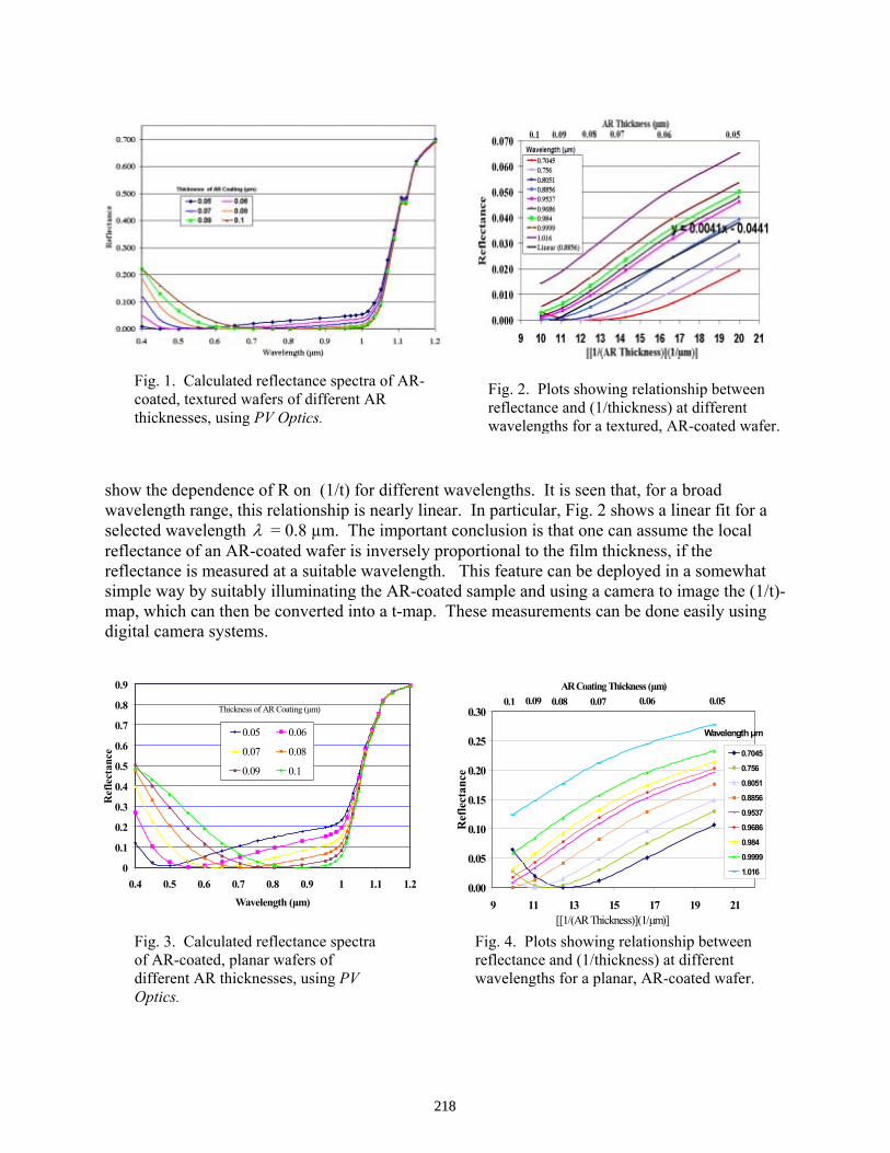
show the dependence of R on (1/t) for different wavelengths. It is seen that, for a broad wavelength range, this relationship is nearly linear. In particular, Fig. 2 shows a linear fit for a selected wavelength λ = 0.8 µm. The important conclusion is that one can assume the local reflectance of an AR-coated wafer is inversely proportional to the film thickness, if the reflectance is measured at a suitable wavelength. This feature can be deployed in a somewhat simple way by suitably illuminating the AR-coated sample and using a camera to image the (1/t)-map, which can then be converted into a t-map. These measurements can be done easily using digital camera systems.
Fig. 1. Calculated reflectance spectra of AR-coated, textured wafers of different AR thicknesses, using PV Optics.
Fig. 2. Plots showing relationship between reflectance and (1/thickness) at different wavelengths for a textured, AR-coated wafer.
Fig. 3. Calculated reflectance spectra of AR-coated, planar wafers of different AR thicknesses, using PV Optics.
Fig. 4. Plots showing relationship between reflectance and (1/thickness) at different wavelengths for a planar, AR-coated wafer.
0
0.1
0.2
0.3
0.4
0.5
0.6
0.7
0.8
0.9
0.4 0.5 0.6 0.7 0.8 0.9 1 1.1 1.2
Wavelength (µm)
Ref
lect
ance
0.05 0.06
0.07 0.08
0.09 0.1
Thickness of AR Coating (µm)
AR Coating Thickness (µm)
0.00
0.05
0.10
0.15
0.20
0.25
0.30
9 11 13 15 17 19 21[[1/(AR Thickness)](1/µm)]
Ref
lect
ance
0.7045
0.756
0.8051
0.8856
0.9537
0.9686
0.984
0.9999
1.016
Wavelength µm
0.1 0.09 0.08 0.07 0.06 0.05
218
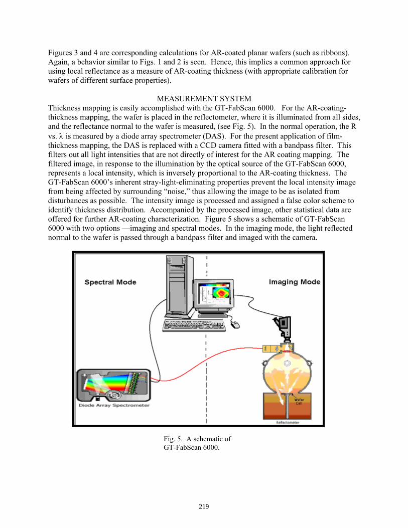
Figures 3 and 4 are corresponding calculations for AR-coated planar wafers (such as ribbons). Again, a behavior similar to Figs. 1 and 2 is seen. Hence, this implies a common approach for using local reflectance as a measure of AR-coating thickness (with appropriate calibration for wafers of different surface properties).
MEASUREMENT SYSTEM
Thickness mapping is easily accomplished with the GT-FabScan 6000. For the AR-coating-thickness mapping, the wafer is placed in the reflectometer, where it is illuminated from all sides, and the reflectance normal to the wafer is measured, (see Fig. 5). In the normal operation, the R vs. λ is measured by a diode array spectrometer (DAS). For the present application of film-thickness mapping, the DAS is replaced with a CCD camera fitted with a bandpass filter. This filters out all light intensities that are not directly of interest for the AR coating mapping. The filtered image, in response to the illumination by the optical source of the GT-FabScan 6000, represents a local intensity, which is inversely proportional to the AR-coating thickness. The GT-FabScan 6000’s inherent stray-light-eliminating properties prevent the local intensity image from being affected by surrounding “noise,” thus allowing the image to be as isolated from disturbances as possible. The intensity image is processed and assigned a false color scheme to identify thickness distribution. Accompanied by the processed image, other statistical data are offered for further AR-coating characterization. Figure 5 shows a schematic of GT-FabScan 6000 with two options —imaging and spectral modes. In the imaging mode, the light reflected normal to the wafer is passed through a bandpass filter and imaged with the camera.
Fig. 5. A schematic of GT-FabScan 6000.
219
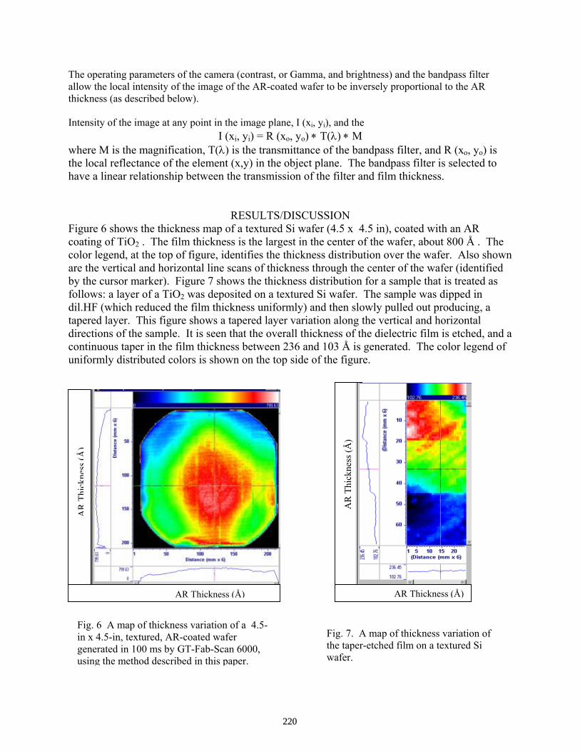
The operating parameters of the camera (contrast, or Gamma, and brightness) and the bandpass filter allow the local intensity of the image of the AR-coated wafer to be inversely proportional to the AR thickness (as described below). Intensity of the image at any point in the image plane, I (xi, yi), and the
I (xi, yi) = R (xo, yo) ∗ T(λ) ∗ M where M is the magnification, T(λ) is the transmittance of the bandpass filter, and R (xo, yo) is the local reflectance of the element (x,y) in the object plane. The bandpass filter is selected to have a linear relationship between the transmission of the filter and film thickness.
RESULTS/DISCUSSION Figure 6 shows the thickness map of a textured Si wafer (4.5 x 4.5 in), coated with an AR coating of TiO2 . The film thickness is the largest in the center of the wafer, about 800 Å . The color legend, at the top of figure, identifies the thickness distribution over the wafer. Also shown are the vertical and horizontal line scans of thickness through the center of the wafer (identified by the cursor marker). Figure 7 shows the thickness distribution for a sample that is treated as follows: a layer of a TiO2 was deposited on a textured Si wafer. The sample was dipped in dil.HF (which reduced the film thickness uniformly) and then slowly pulled out producing, a tapered layer. This figure shows a tapered layer variation along the vertical and horizontal directions of the sample. It is seen that the overall thickness of the dielectric film is etched, and a continuous taper in the film thickness between 236 and 103 Å is generated. The color legend of uniformly distributed colors is shown on the top side of the figure.
Fig. 6 A map of thickness variation of a 4.5-in x 4.5-in, textured, AR-coated wafer generated in 100 ms by GT-Fab-Scan 6000, using the method described in this paper.
Fig. 7. A map of thickness variation of the taper-etched film on a textured Si wafer.
AR
Thic
knes
s(Å
)
AR Thickness (Å)
AR
Thi
ckne
ss (Å
)
AR Thickness (Å)
220

CONCLUSION A new technique for rapid mapping of AR-coating thickness has been developed. The rapid-mapping capability makes the instrument well suited for online process monitoring and valuable to ensuring a good process control and enhancing reliability. The advantages of this technique are that it is very rapid—maps the entire wafer in one measurement in less than 100 ms; the measurement is insensitive to the nature of the wafer surface (works on planar, rough, and textured wafers); because a digital image is obtained, a variety statistical parameters can be quickly identified; and that the system is capable of online process monitoring. Use of this technique is expected to be very valuable in optimizing hydrogen passivation and the fire-through metallization process. In particular, current method(s) of AR-coating deposition need to be evaluated for non-uniformities in the coating thickness and its effects on cell performance. For example, Fig. 8 shows a map of AR thickness on a wafer that was in the same batch for AR-coating deposition as the wafer in Fig. 6. As seen, the general distribution pattern of both wafers is the same, but details of thickness profile are considerably different. It may no longer be sufficient to relate AR-coating effects simply to the loss in photocurrent. It is expected that large variations in the AR-coating thickness can be detrimental to achieving high cell performance in fire-though contact processing.
REFERENCES 1. B. L. Sopori, “Principle of a new reflectometer for measuring dielectric film thickness on
substrates of arbitrary characteristics,” Rev. Sci. Instrum. 59(5), 725, 1988. 2. Bhushan Sopori, U. S. Patent No. 6,275,295. 3. B. L. Sopori, Y. Zhang, W. Chen, and J. Madjdpour, “Silicon solar cell process monitoring
by PV Reflectometer,” IEEE PVSC, Anchorage, AK, Sept. 2000.
Fig. 8. A thickness map of a 4.5-in x 4.5-in, textured, AR coated wafer from the same batch as the wafer shown in Fig. 6.
AR
Thi
ckne
ss (Å
)
AR Thickness (Å)
221

Aluminum Gettering and Dissolution of Cu3Si Precipitates in Silicon
T. Buonassisi1,2, A.A. Istratov1,2, M.A. Marcus3, and E.R. Weber2,1
1 Materials Sciences Division, Lawrence Berkeley National Laboratory, Berkeley, CA 94720 2 Department of Materials Science, University of California at Berkeley, Berkeley, CA 94720
3 Advanced Light Source, Lawrence Berkeley National Laboratory, Berkeley, CA 94720 In this study we determined segregation coefficient of copper in aluminum and inves-tigated the mechanism of Al gettering of copper by using synchrotron-based analytical mi-croprobe techniques. A 700 µm-thick CZ sample containing 106 cm-3 oxygen precipitates was copper-contaminated by a diffusion anneal at 1200°C. After the sample was cooled to room temperature, a 5 µm aluminum layer was evaporated onto one surface of the sample through a wire mesh. Subsequently, the sample was annealed at 800°C for 2 hours in forming gas ambient in a horizontal furnace to getter the Cu to the Al. The sample was then removed from the furnace onto an aluminum plate, where it cooled rapidly. The aluminum gettering layer was subsequently observed with an optical microscope (Fig. 1a) and scanned using synchrotron-based X-ray fluorescence microscopy technique (µ-XRF, Fig. 1b), revealing copper present only where aluminum was deposited through the wire mesh. No Cu was detected in an Al layer of the same thickness evaporated onto a float zone control sample that did not receive any intentional contamination. The effectiveness of aluminum gettering for the removal of Cu from bulk Si is a likely indication of a weak bind-ing energy of Cu to Cu3Si clusters (see other contribution by Buonassisi et al. in this volume entitled Distribution and Chemical State of Cu-rich Clusters in Silicon), unlike what one would expect from an oxidized species. The chemical state of Cu in the Al gettering layer provides an indication of the getter-ing mechanism. Chemical identification performed by extended X-ray absorption fine struc-ture microspectroscopy (µ-EXAFS) revealed that the copper gettered to thicker regions of Al (indicated by a dashed arrow in Fig. 1b) has formed a species very similar to that identified in Ref. 1, a dilute Cu solution in Al (Fig. 2). This result directly confirms the generally accepted opinion [2] that the mechanism of segregation of metals in aluminum is their higher solubility in the liquid phase. A different chemical state of Cu is identified in thinly dispersed aluminum particles on the backside (indicated by a solid arrow in Fig. 1b). The µ-EXAFS from this location (Fig. 3), while not making a perfect match with any of our standards, is most similar to the θ-Al2Cu standard material of Ref. 1. Precipitates of θ-Al2Cu, which are known to form within aluminum layers, are very unstable and dissolve rapidly at temperatures above 400°C. There-fore, there is no indication that the presence of this phase would change the segregation coef-ficient of copper to aluminum at higher temperatures. At the moment, it cannot be unambigu-ously determined why this different phase of copper is observed only in thin Al layers. One may speculate that the percentage composition of copper in the thin aluminum layer in-creased substantially during cool-down, either via relaxation gettering of copper from the bulk and/or a strong temperature dependence of the segregation coefficient. It has been ob-served, for example, that Al is effective at gettering Cu from Si at temperatures as low as 540°C [3]. The increased solubility of Cu in the Al gettering layer, the presumably weak binding energy of Cu to Cu3Si, and the high diffusivity of Cu in Si suggest that Al gettering is indeed very effective for removing Cu from bulk silicon. However, this does not imply that a stan-dard Al gettering procedure, with a micron of Al and an 800°C anneal, would remove all Cu
222
from the Si bulk to below the detection limit. The residual concentration of Cu in the silicon wafer after Al gettering is determined by three parameters, the thicknesses of the silicon sub-strate and of the aluminum layer, and the segregation coefficient, i.e. the ratio of the equilib-rium solubilities of copper in aluminum (cAl) and in silicon (cbulk) at a given temperature:
kT ≡cAl
cbulk (1)
The segregation coefficient k can be derived experimentally from the µ-XRF map in Fig. 1b by taking into consideration the Cu counts in the thick Al layer vs. the counts in the bare silicon bulk, the thicknesses of these two layers, and the XRF attenuation lengths of the Cu-Kα fluorescence signal in these two layers. The segregation coefficient as defined in Eq. 1 for the sample shown in Fig. 1b is estimated to be at least (1-2)×103. This value is a lower estimate since a parasitic background Cu signal measured by the fluorescence detector, al-though much too weak to disturb µ-XAS measurements, is likely to have produced an artifi-cially high Cu count rate on the bare silicon bulk. Nevertheless, this value is close to what one would expect assuming a solubility of Cu in the Al-Si layer of about 0.1-1 at. % and a Cu solubility in Si at 800°C of 5.5×1016 cm-3, while being consistent with earlier results [4] pro-viding k > 1×10³. With the estimated segregation coefficient k = 2×10³ and typical solar cell parameters for wafer thickness d = 240 µm and Al layer thickness w = 1 µm, one can predict from the following equation (from Ref 5):
[Cu] in Bulk After Gettering
[Cu] in Bulk Before Gettering ≡
cbulk
co
= cbulk
cbulk ⋅ d + cAl ⋅ w
d
= 1
1+k ⋅ w
d
(2)
that an upper limit of about 90% of the total copper content can be gettered from the bulk by segregation to the Al layer with k=103. With k = 104 and all other parameters constant, the same calculation predicts an upper limit of over 97%. It follows from Eq. 2 that the much lower thickness of the Al layer than that of the Si wafer leads to a much faster increase of Cu concentration in the Al layer than its decrease in Si. Thus, when equilibrium is reached, Cu concentration in the bulk may only decrease by a relatively small factor. It is likely that the remaining dissolved Cu in the bulk will re-precipitate during cooling, especially with the high density of structural defects present in mc-Si. This is consistent with numerous µ-XRF observations of Cu-rich clusters at structural defects in Al-gettered or fully processed mc-Si [6-9]. Irrespective of the precise value of k, it follows from Eq. 2 that thicker Al layers should result in the removal of a larger fraction of the total Cu from the bulk during gettering. Other mechanisms may also be responsible for retarding or inhibiting the complete dissolution and removal of all Cu3Si clusters during gettering. Cu3Si clusters, or individual Cu atoms, may be stabilized either by the lattice strains of adjacent structural defects or other metal clusters [6,10,11]. Specifically, the chemical interactions between Cu and other metal species (of which mc-Si contains an abundance [8]) are not well understood at the present time. The singular result of all these effects would likely be an effective segregation coeffi-cient k' for mc-Si which is lower than that for single-crystalline silicon. As a consequence, more Cu is likely to remain within bulk mc-Si after Al gettering than sc-Si. Additionally, it has also been suggested that relatively slowly-diffusing Si self-interstitials may play a rate-
223
limiting role in precipitate dissolution, as these are needed to counterbalance the volumetric shrinkage associated with the dissolving Cu3Si precipitates [12]. In any case, a two-step alu-minum gettering treatment, consisting of a high temperature step to fully dissolve Cu from Cu3Si clusters, followed by a gradual lowering of the temperature to promote the diffusion of Cui
+ to the Al gettering layer, may be a viable alternative to optimize the removal of Cu from bulk Si. In conclusion, aluminum gettering is shown to be very effective at gettering copper from silicon, a natural consequence of the fact that copper is only weakly bound to copper silicide particles, and thus at higher temperatures Cu can readily diffuse to the Al layer where its solubility was experimentally determined to increase by at least three orders of magnitude. µ-EXAFS reveals that the chemical state of Cu in thick Al gettering layers matches well that of a solid solution of Cu in Al, consistent with the notion that the mechanism of segregation of copper in aluminum is its higher solubility in the liquid phase, which does not necessarily imply any chemical bonding of copper to aluminum. Despite its effectiveness, Al gettering does not necessarily remove all Cu from the bulk. The segregation coefficient and the relative thicknesses of the Al and Si layers determine the ungettered fraction of Cu, which may promptly re-precipitate at the most stable heterogeneous nucleation sites within the bulk upon cooling. In addition, a few possible mechanisms retarding the dissolution of Cu3Si clusters have been described, namely stabilization by the lattice strains of nearby structural defects and/or other metal clusters. Acknowledgements We would like to acknowledge helpful discussions with S.K. Estreicher and his team. This study was supported by NREL subcontract AAT-2-31605-03. The operations of the Ad-vanced Light Source at Lawrence Berkeley National Laboratory are supported by the Direc-tor, Office of Science, Office of Basic Energy Sciences, Materials Sciences Division, of the US Department of Energy under Contract No. DEAC03-76SF00098. Use of the Advanced Photon Source was supported by the US Department of Energy, Office of Science, Office of Basic Energy Sciences, under Contract No. W-31-109-ENG-38. References: [1] M. A. Marcus and J. E. Bower, Journal of Applied Physics 82, 3821 (1997). [2] M. Apel, I. Hanke, R. Schindler, et al., Journal of Applied Physics 76, 4432 (1994). [3] R. D. Thompson and K. N. Tu, Applied Physics Letters 41, 440 (1982). [4] L. A. Verhoef, P. P. Michiels, S. Roorda, et al., Materials Science & Engineering B B7, 49 (1990). [5] H. Hieslmair, S. A. McHugo, A. A. Istratov, et al., in Properties of Crystalline Silicon, edited by
R. Hull (INSPEC, Short Run Press, Exeter, 1999), p. 775. [6] S. A. McHugo, Applied Physics Letters 71, 1984 (1997). [7] A. A. Istratov, H. Hieslmair, O. F. Vyvenko, E. R. Weber, and R. Schindler, Solar Energy Materi-
als & Solar Cells 72, 441 (2002). [8] A. A. Istratov, T. Buonassisi, R. J. McDonald, A. R. Smith, R. Schindler, J. A. Rand, J. P. Kalejs,
E. R. Weber, Journal of Applied Physics 94, 6552 (2003). [9] T. Buonassisi, O. F. Vyvenko, A. A. Istratov, E. R. Weber, G. Hahn, D. Sontag, J. P. Rakotonia-
ina, O. Breitenstein, J. Isenberg, and R. Schindler, Journal of Applied Physics 95, 1556 (2004).
[10] M. Kittler and W. Seifert, Solid State Phenomena 95-96, 197 (2004). [11] R. C. Dorward and J. S. Kirkaldy, J. Mater. Sci. 3, 502 (1968). [12] S. A. McHugo, A. Mohammed, A. C. Thompson, B. Lai, and Z. Cai, Journal of Applied Physics
91, 6396 (2002).
224

Fig. 1. (a) Optical microscope image of the surface of a Cu-contaminated CZ-Si sample with 106 cm-3 oxygen precipitates. This sample was annealed at 800°C for 2 hours after squares of aluminum were evaporated onto the surface through a wire mesh. (b) Cu-Ka x-ray fluorescence microscopy image for the region highlighted in (a) shows the high concentration of Cu gettered to the thick Al squares (note log XRF scale), and the fine dusting of Cu in tiny Al particles between the squares,
indicative that even a tiny bit of Al is a very effective getterer of Cu. The dashed and solid arrows denote locations of µ-EXAFS scans in Figures 2 and 3, respectively.
Fig. 2. EXAFS of Cu gettered to thick regions of Al (dashed arrow in Fig. 1b). Notice the fairly good agreement with the standard material of dilute Cu dissolved in Al. (Standards from Ref. 1.)
Fig. 3. EXAFS of Cu gettered to thin regions of Al (solid arrow in Fig. 1b). Notice the difference between this spectrum and that of the thicker regions of Al (Fig. 2). The progression of the measured spectrum from dilute Cu in Al to q-Al2Cu indicates an increasing saturation of Al with gettered Cu. (Standards from Ref. 1.)
225

Differences and Similarities Between Metal Clusters in mc-Si Materials from Different Manufacturers
T. Buonassisi1,2, A. A. Istratov1,2, T. F. Ciszek3, D. W. Cunningham4, A. M. Gabor5, R. Jonczyk6,
R. Schindler7, M. Sheoran8, A. Upadhyaya8, A. Rohatgi8, B. Lai9, Z. Cai9, M. A. Marcus10, E. R. Weber2,1 1. Lawrence Berkeley National Laboratory, Berkeley, CA 2. Department of Materials Science, University of California, Berkeley, CA 3. Formerly: National Renewable Energy Laboratory, Golden, CO / Presently: Siliconsultant, Evergreen, CO; 4. BP Solar, Frederick, MD 5. Evergreen Solar, Marlboro, MA 6. GE Energy, Newark, DE 7. Fraunhofer Institute for Solar Energy Systems, Freiburg, Germany 8. Georgia Institute of Technology, Atlanta, GA 9. Advanced Photon Source, Argonne National Laboratory, Argonne, IL 10. Advanced Light Source, Lawrence Berkeley National Laboratory, Berkeley, CA I. Nature of Metal Contamination The nature of metal contamination was studied in a number of as-grown and processed multicrystalline silicon (mc-Si) materials by a suite of synchrotron microprobe-based techniques. X-ray fluorescence microscopy (µ-XRF) was used to locate metal-rich clusters and identify their elemental composition, and x-ray absorption microspectroscopy (µ-XAS) was used to study the chemical composition of these clusters. X-ray beam induced current (XBIC) [1], a technique analogous to laser beam induced current, was used to map the minority carrier diffusion length. I-A. Cast mc-Si A variety of metal-rich clusters have been observed in different as-grown cast mc-Si materials, which were obtained from two different vendors and will be denoted as "material A" and "material B", respectively. In as-grown material A, metal-rich clusters containing copper, nickel, and cobalt were frequently observed at grain boundaries in the lower regions of the ingot, and Ni and Cu in the upper regions of the ingot. The chemical state of the copper is copper silicide (Cu3Si), and the nickel is also believed to be in silicide form (NiSi2). The metal-rich precipitates in the upper parts of the ingot demonstrated a more homogeneous distribution along the grain boundaries than in lower regions of the ingot (see Fig. 1), suggesting that different cooling rates in the different regions of the ingot influenced the final distribution of metal silicide precipitates. One cannot exclude that differences in the precipitation environments (e.g. structural defects) also played a role. In addition to the smaller metal silicide clusters, some more unusual metal-rich clusters were also present in the material: one cluster contained a fair amount of tungsten, while another contained titanium, both offset by a few microns from the nearest grain boundary. The titanium cluster measured approximately 8×15 µm2, which is still far larger than what could form from via the localized precipitation of interstitial titanium from adjacent silicon within a radius of 350 µm, which is equal to the diffusion distance of interstitial Ti at 1200°C during eight hours. For this reason, and because of the curious chemical state of the particle (believed to be some form of oxide, but currently not matched with any of our standards) it is believed the Ti-rich cluster is an inclusion, i.e. a foreign particle engulfed by the advancing solidification front. In material B, multiple Fe-rich clusters measuring <60 nm in diameter (along the dimensions perpendicular to the crystal growth direction) were detected along grain boundaries. The distance separating these iron-rich particles at the recombination-active grain boundaries averaged between 8 and 40 µm, much less than the minority carrier diffusion length in good regions of the material. Nickel and copper accompanied some of the iron-rich clusters in the as-grown material. The chemical states of these metal-rich nanoparticles were determined to be metal silicides (e.g. FeSi2, Cu3Si). In addition to these metal silicide nanoprecipitates, a few large iron oxide (Fe2O3) particles measuring >1 µm in diameter were detected, accompanied by other metals such as Cr, Mn, Ca, and possibly Ti. Because of their size and composition, these particles are believed to be inclusions of foreign particles that entered the melt and were incorporated into the finished crystal. In both materials types A and B, copper- and nickel-rich clusters were either drastically reduced in size or not detectable after as-grown materials were processed into solar cells at Georgia Tech and Fraunhofer ISE, while iron-rich clusters frequently remained, although often reduced in size. This can be understood considering the differences in solubility and diffusivity between the different metal species. Precipitates composed of copper and nickel, both of which have high interstitial solubility and diffusivity in silicon, can dissolve rather rapidly during a
226

heat treatment. Precipitates formed of iron, on the other hand, dissolve slower due to the reduced diffusivity and solubility of interstitial iron in silicon [2]. I-B. Sheet material In as-grown sheet material, metal-rich clusters consisting of micron-sized Fe, Cr, and Ni particles were evident in abundance towards the back regions of the material, and to a much lesser extent, towards the front. This combination of metals suggests stainless steel contamination, likely introduced in particulate form in the feedstock. The chemical states of metals in these clusters were identified by µ-XAS to be metal silicides (FeSi2, CrSi2, NiSi2). Because of the fast growth rates of sheet material, and the fact that the melting temperature of iron oxide is 150°C above that of silicon, one would expect to find an abundance of oxidized inclusions if these foreign impurity-rich particles were originally introduced in oxidized form. This suggests that these (Fe+Cr+Ni)-rich particles were originally introduced into the melt in metallic form. These stainless steel particles are likely to have dissolved to some extent during the crystal growth process, contaminating neighboring structural defects as a result. Evidence for this lies in the observation of a high density of iron silicide nanoprecipitates at grain boundaries and at intragranular defects (Fig. 2). Since voids have been identified in this material through previous studies [3], the intragranular defect clusters composed of Fe-rich nanoparticles, such as that in Fig. 2, are likely to consist of iron precipitated at the internal surfaces of voids within the bulk. Were all the iron precipitated at grain boundaries and intragranular defects to be dissolved homogeneously throughout the sample, estimates with standard-calibrated µ-XRF measurements suggest that bulk concentrations of 1015-16 Fe/cm3 would be reached. This value matches well with neutron activation analyses (NAA) performed on this material [4]. The accumulation of metals at selected locations leads to the decrease of metal point defects and smaller clusters elsewhere, thus improving the diffusion lengths in those regions. A complete summary of these findings will be soon available elsewhere [5]. I-C. Ribbon material Several regions of a fully-processed Evergreen string ribbon material sample were analyzed by µ-XRF, but no metal-rich clusters with diameter > 30 nm were detected. Nevertheless, our NAA measurements presented at this workshop last year indicate that ribbon materials tend to have similar metal content as cast materials (edge-defined film-fed growth (EFG) ribbon and cast both contained ~1014 Fe cm-3, over an order of magnitude less than sheet material). Two possibilities exist to explain this: (1) the metal content of Evergreen ribbon material is lower than EFG material, or (2) metals are distributed in Evergreen material in a greater number of clusters, but each with an average size below the current detection limit (diameter ~ 30 nm). The faster growth speeds of ribbon materials relative to cast mc-Si are likely to result in a more homogeneous distribution of smaller clusters (see also other contributions by our group in this volume). I-D. Multicrystalline Float Zone Multicrystalline float zone (mc-FZ) samples contaminated with copper during crystal growth were also analyzed. More information about mc-FZ crystal growth can be found in Ref [6]. Copper was found to form rather large, recombination-active clusters along structural defects such as grain boundaries. In intragranular regions, the spatial density of copper precipitates (presumably at dislocations) had a large impact on the minority carrier diffusion length, as can be seen in Fig. 3. Areas with fewer Cu-rich clusters exhibited higher minority carrier diffusion lengths. The chemical state of all measured Cu-rich clusters in these samples was copper silicide, Cu3Si. II. Similarities Metals in all samples exhibited a tendency to precipitate at structural defects, especially two-dimensional defect surfaces such as grain boundaries. In certain materials, metals were also concentrated at intragranular locations, presumably associated with structural defects. When two or more metal species were present in high concentrations in the same sample, often these metals could be observed precipitated at the same locations (or within the limits of the spatial resolution of the technique). It may be that the nucleation and growth of many phases of metal silicide are favorable at the same precipitation sites, or perhaps, that metal silicide precipitates of different metal species minimize the energy required for formation and growth by precipitating near each other (e.g. compensation of lattice strains between Cu3Si/FeSi2). The large majority of metal-rich clusters observed in all materials were in a metal-silicide chemical state. Only very few large metal clusters were oxidized. Those particles, from their elemental composition and size, appear to be introduced into the melt from a foreign source (such as impurity particles in the feedstock), and before fully dissolving, they are incorporated into the final silicon crystal as inclusions. Dissolved metals from these
227

particles are likely to be the source of the smaller and more distributed metal-silicide nanoparticles observed at grain boundaries and in intragranular defect clusters in sheet material. III. Differences Between the different types of materials, the most significant differences are observed in the size and spatial distribution of metal-rich precipitates. For example, micron-sized clusters of metal-rich particles are found at intragranular locations in sheet material, while only isolated intragranular metal-rich nanoparticles have been observed in cast mc-Si material. In addition, the sizes and distances of metal-rich particles at grain boundaries in as-grown cast mc-Si and sheet material differs as well. In a sheet material sample scanned with high-resolution µ-XRF, iron silicide particles roughly 23 nm in radius are separated by 2-3 µm, while in a cast mc-Si sample, these particles were roughly 30 nm in radius and separated by 8-9 µm. In other words, metal-rich particles may be larger in average size and spaced by larger distances, or smaller in size and closer together. These distributions were found to vary as a function of material and thermal history. There are also differences in distribution observed within the same type of material, e.g. cast mc-Si. Whereas relatively larger and more isolated Cu- and Ni-rich clusters were observed at a grain boundary at the bottom of the ingot, smaller and more homogeneously distributed clusters were found at another grain boundary in a sample from the top of the ingot. This could be due to differences in the cooling rates of the two areas of the ingot, or possibly, due to differences in the density of crystal lattice defects which serve as nucleation sites for the metal-rich precipitates at the top and at the bottom of the ingot. It is known that the metal distribution in mc-Si can be affected by a combination of one or more of the following factors: (a) feedstock impurity content, (b) crucible and crucible lining impurity content, (c) contamination by foreign particles during growth, and (d) growth parameters (see other contributions by Istratov et al. and Buonassisi et al. in these proceedings for more details about the effect of thermal treatments and cooling rate on metal precipitate formation and distribution). Variations between different materials analyzed in this study are believed to be due to one or more of these factors. Variations are even expected from run to run within one type of material, as parameters such as the feedstock impurity content may vary. As this affects the final solar cell device performance, strict control of all variables is required to meet production quality standards. Summary Comparative analysis of distribution of metal clusters in multicrystalline silicon samples obtained from several industrial partners and from NREL revealed that there are many similarities between chemical structure and distribution of these clusters: the majority of metal clusters are metal-silicide precipitates (with the exception of a few larger particles containing oxidized metals which appear to be incompletely dissolved foreign particles included into the silicon crystal); the particles are predominantly found either at grain boundaries or sometimes at intragranular defect clusters. Most analyzed particles consist of copper, nickel, and iron, although other particles containing chromium, tungsten, and titanium were also detected. Despite all these similarities, the distribution of particles and their density varied from one growth technique to another, and from one part of the ingot to the other part, thus suggesting that the crystal growth parameters, particularly the cooling regime, and the density of lattice defects may be an important factor determining the final distribution and location of metals in the solar cells. Acknowledgements This study was supported by NREL subcontract AAT-2-31605-03. The operations of the Advanced Light Source at Lawrence Berkeley National Laboratory are supported by the Director, Office of Science, Office of Basic Energy Sciences, Materials Sciences Division, of the US Department of Energy under Contract No. DEAC03-76SF00098. Use of the Advanced Photon Source was supported by the US Department of Energy, Office of Science, Office of Basic Energy Sciences, under Contract No. W-31-109-ENG-38. References [1] O. F. Vyvenko, T. Buonassisi, A. A. Istratov, et al., J. Appl. Phys. 91, 3614-3617 (2002). [2] P. S. Plekhanov, R. Gafiteanu, U. M. Gosele, and T. Y. Tan, J. Appl. Phys. 86, 2453-2458 (1999). [3] J. Rand, G. Rozgonyi, R. Jonczyk, et al., 12th Workshop on Cryst. Silicon Solar Cell Mat. & Proc. (Breckenridge, CO, 2002). [4] A. A. Istratov, T. Buonassisi, R. J. McDonald, et al., J. Appl. Phys. 94, 6552-6559 (2003). [5] T. Buonassisi, A. A. Istratov, M. Heuer, M. Marcus, R. Jonczyk, J. Isenberg, B. Lai, Z. Cai, S. Heald, W. Warta, R.
Schindler, and E. R. Weber, Submitted to J. Appl. Phys. (2004). [6] T. F. Ciszek, and T. H. Wang, Journal of Crystal Growth 237-239, 1685-1691 (2002).
228
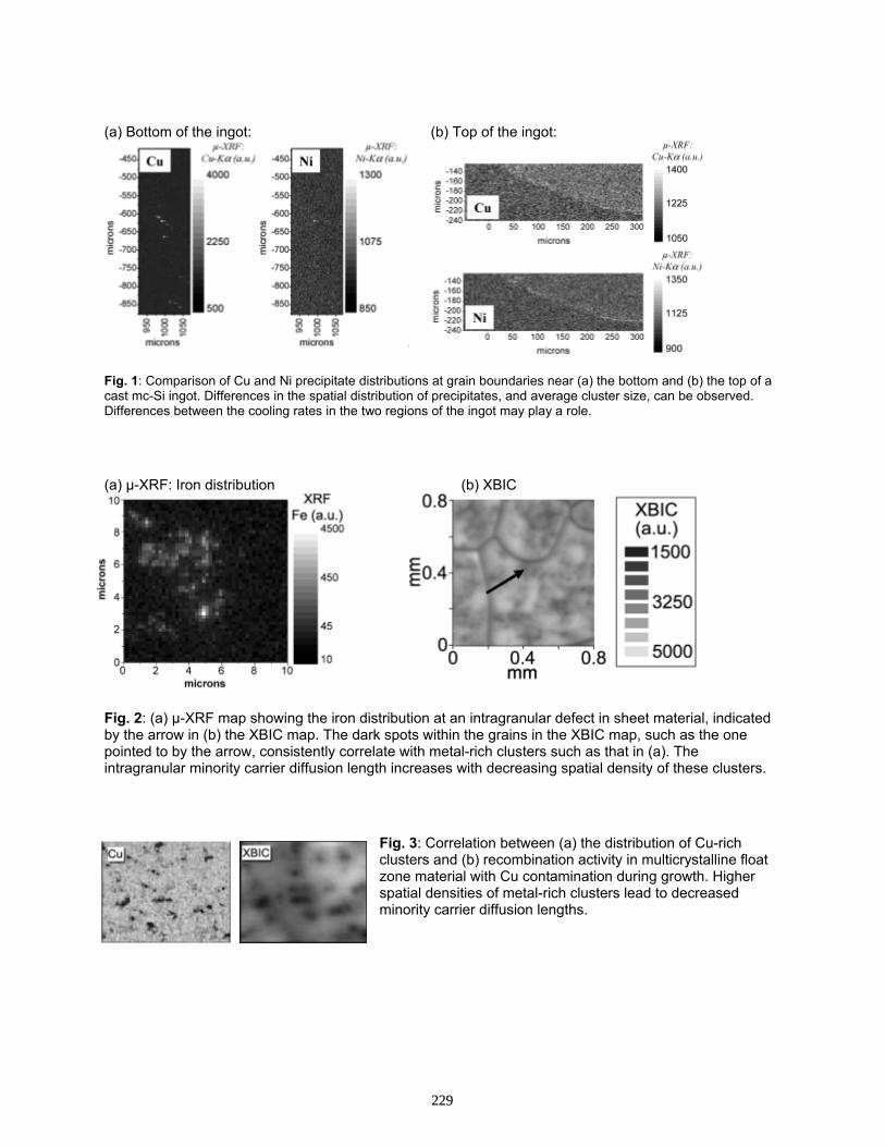
(a) Bottom of the ingot:
(b) Top of the ingot:
Fig. 1: Comparison of Cu and Ni precipitate distributions at grain boundaries near (a) the bottom and (b) the top of a cast mc-Si ingot. Differences in the spatial distribution of precipitates, and average cluster size, can be observed. Differences between the cooling rates in the two regions of the ingot may play a role. (a) µ-XRF: Iron distribution (b) XBIC
Fig. 2: (a) µ-XRF map showing the iron distribution at an intragranular defect in sheet material, indicated by the arrow in (b) the XBIC map. The dark spots within the grains in the XBIC map, such as the one pointed to by the arrow, consistently correlate with metal-rich clusters such as that in (a). The intragranular minority carrier diffusion length increases with decreasing spatial density of these clusters.
Fig. 3: Correlation between (a) the distribution of Cu-rich clusters and (b) recombination activity in multicrystalline float zone material with Cu contamination during growth. Higher spatial densities of metal-rich clusters lead to decreased minority carrier diffusion lengths.
229

Evidence for segregation of iron at grain boundaries in polycrystalline and multicrystalline silicon
A.A.Istratov(a), T.Buonassisi(a), W.Huber(b), and E.R.Weber(a)
(a) Department of Materials Science, University of California, Berkeley, CA 94720 (b) Sumitomo Mitsubishi Silicon, Fremont, CA 94538
Gettering in multicrystalline silicon solar cells is a competitive process between precipita-
tion/segregation of metals at intentionally introduced gettering sites and lattice defects present in the bulk of mc-Si wafers. Gettering can be efficient only if intentionally introduced gettering sites have a higher density and/or stronger binding energy for metals than defects in the bulk of the wa-fer. Therefore understanding of the mechanisms of trapping of metals at different extended defects is essential for improving gettering techniques. Grain boundaries (GBs) are efficient gettering sites for metals in multicrystalline and polycrystalline silicon. The gettering properties of GBs are de-termined by a combination of two mechanisms, relaxation (i.e., precipitation of supersaturated im-purities at extended defects during wafer cooling) and segregation (i.e., increased equilibrium metal solubility near grain boundaries and dislocations due to local distortion of the lattice). While both segregation and relaxation mechanisms lead to agglomeration of metals at grain boundaries, segregated impurities are more difficult to remove by gettering than precipitated ones. The co-existence of relaxation and segregation mechanisms of gettering of metals to GBs has been pro-posed long ago; however, quantitative characteristics of these two gettering mechanisms were not available. In this article we propose experimental procedures which allowed us to quantify segre-gation and relaxation gettering of iron by grain boundaries and discuss implications of these results for multicrystalline silicon solar cells.
In theory, one could separate the contribution of segregation gettering from the relaxation component by quenching a sample to room temperature sufficiently fast to freeze-in the high-temperature distribution of metals. However, even such well established quenching baths as sili-cone oil (estimated average quenching rate 100-250 K/s), ethylene glycol (1000 K/s) and 10% NaOH solution (2000 K/s) [1] turn out to be not sufficiently fast for this purpose. Since the diffu-sion coefficients of impurities in silicon depend exponentially on temperature, the quenching rate required to freeze-in the metal distribution also exponentially increases with the annealing tem-perature and gets unrealistically high at temperatures above 900-1000oC.
In our experiments, we used structures consisting of thin polysilicon layers deposited on CZ-grown silicon wafers. The advantage of polysilicon is that it has a high GB density and can easily be deposited on a CZ substrate. To separate contributions of segregation and relaxation get-tering, SIMS depth profile of Fe in quenched polySi/Si structure was taken to a depth of 30-40 mi-crons into the substrate to the point where iron concentration reaches its equilibrium solubility (Fig. 1). The sample analyzed in Fig 1 consisted of 11 µm of nominally undoped polysilicon de-posited on top of a p- silicon substrate. The sample was contaminated from the backside by scratching with an iron wire, annealed in a vertical furnace at 1150oC in N2 + 5% H2 ambient for 90 min, and quenched in silicone oil.
A decrease in the iron concentration in the substrate towards the interface with polysilicon stems from relaxation gettering of iron during the silicone oil quench, whereby supersaturated iron diffuses from the substrate to the polysilicon layer and precipitates there, primarily in the areas close to the polySi/substrate boundary. The total amount of iron that was gettered in the poly-Si layer due to a combination of segregation and relaxation mechanisms can be determined, in the
230

units of Fe atoms per cm2 of the sample surface, by integrating the area “A” of the plot in Fig. 1a between the SIMS data in polySi and the equi-librium iron solubility. The total amount of iron that diffused into the polysilicon layer during cooling can be calculated by integrating the area “B” in the substrate. By performing the integra-tion, one obtains A=1.44×1013 cm-2 and B=2.52×1012 cm-2. Since the area A is 6.4 times greater than the area B, relaxation gettering alone cannot account for all iron accumulated in concentrations above its equilibrium solubility in the area B. The segregation coefficient k can be determined as follows: k= S(poly)/S(substrate) =(Feeq+(A-B)/d)/Feeq≈2.6, where Feeq is the equilibrium Fe solubility in silicon at the diffusion temperature, d is the thickness of the poly-Si layer, and S(poly) and S(substrate) are the solubilities of iron in poly-silicon and in the substrate.
In order to obtain a quantitative measure of the relaxation gettering efficiency of the polysilicon layer (which is characterized in Ham’s model [2] by the product of the precipi-tation sites density n times their radius r0), we performed computer modeling of gettering of iron during cooling. The algorithm of the getter-ing simulator used for this analysis is described
in detail elsewhere [3]. The parameters of the model (k, n, and r0) were varied to obtain the best fit, shown in Fig. 1b. To demonstrate the sensitivity of the fit to the nr0 product, two additional curves (dashed lines) with the nr0 ten times greater and smaller than the fitted value are also shown. The segregation coefficient obtained from the fit is k=2.2, which is close to the value determined from the Fig. 1a. The nr0 product for the polysilicon layer was estimated from the fit as 106 cm-2. This value should be compared to a range of values of nr0 for internal gettering sites in CZ-silicon of 103 - 5×105 cm-2 (see Ref. [4]).
The second experimental procedure which we used to separate the effects of segregation and relaxation gettering consists in using a thin (197 nm SiO2) diffusion barrier between the 0.37 µm polySi and the substrate. The sample was annealed for 8 hours at 1020oC, which was sufficient for iron to diffuse through silicon dioxide and establish its equilibrium distribution at the annealing temperature. On the other hand, the diffusivity of iron in silicon dioxide is too slow to allow iron to diffuse through it during the quench. Therefore, even at relatively slow cooling rates, the con-centration of iron in polysilicon represents its concentration established at the annealing tempera-ture. The segregation coefficient in this sample was determined as k ≈16. Note that this value should not be directly compared with the value obtained from Fig. 1 since the thickness of the polysilicon layer (and possibly the grain size) in these two experiments were different. Addition-ally, it is important to note that polysilicon (and to even greater extent, multicrystalline silicon) is very inhomogeneous and contains both grain boundaries with significant lattice strain which seg-
Depth, microns0 5 10 15 20 25 30
Iron
conc
entra
tion,
cm
-3
1015
1016
1017
nr0=107 cm-2, k*=2.2
nr0=106 cm-2, k*=2.2
nr0=105 cm-2, k*=2.2
1016
2x10¹⁶
3x10¹⁶
ABPOLY SUBSTRATE
Fig. 1. Secondary ion mass spectroscopy depth profile of iron diffused in 11 µm polySi/Si structure at 1150oC and quenched in silicon oil. (a) depth profile plotted using a linear concentration scale. The solid horizontal line is the equilibrium iron solubility at the diffusion temperature. (b) The same depth profile plotted on a logarithmical scale together with the results of numeri-cal modeling. The solid line represents the best fit, the dashed lines are variations of the nr0 product.
231

regate the impurities and relatively unstressed silicon within the grains which has no segregation effect. Hence, the macroscopic segregation coefficient observed in the experiments should depend not only on microscopic structure of GBs, but also on the factors such as grain size and is likely to vary depending on the thickness and growth conditions of the layer. Likewise, the values for k and nr0 reported above should only be used as guidelines of the possible range of values as they can vary from sample to sample.
The probable cause for segregation of iron in polysilicon is a difference in its free energy in perfect silicon lattice and in a distorted lattice near the defects such as dislocations and grain boundaries. This model was used to explain the effects of segregation of arsenic [5], boron [6], and phosphorus [7, 8] to grain boundaries in silicon. Since the lattice is substantially distorted only within very short distances (typically, several lattice constants) from the dislocation cores, one can expect that segregated metals would thinly and homogeneously decorate grain boundaries and dis-locations.
This finding has an important implication for photovoltaics. Since mc-Si contains essen-tially the same type of defects as poly-Si, but in lower density, one can expect segregation getter-ing of iron to be present in mc-Si as well. Hence, it is likely that iron and other transition metals would segregate at grain boundaries and dislocations. Since the distorted area around dislocations is very small and is often confined to just several atomic distances, segregation would lead to decoration of defects with a very thin layer of metal, perhaps less than a monolayer. As it is ener-getically favorable for metals to segregate at grain boundaries as compared to the high crystalline quality areas of the wafer, these segregated metals would be gettering-resistant and can be com-pletely removed by either segregation gettering with much higher segregation coefficient than seg-regation coefficient to grain boundaries, possibly combined with a sufficiently high temperature anneal to overcome the binding energy and dissolve all metals segregated at GBs into the wafer.
It is instructive to make a simple estimate of the capacity of grain boundaries. For simplic-ity, lets approximate each grain with a square with the size d. The area of each square is d2, and the perimeter of each square is 4d. Since each side of the square is simultaneously a side of the adja-cent square, perimeter of grain boundaries per each grain is half of that, i.e., 2d. There are 1/d2 of grains per each cm2 of the sample surface. Hence, the total area of grain boundaries per cm2 of the sample surface in a sample with thickness t is 2t/d, and the total amount of iron that can segregate at the boundaries per cm2 of the wafer surface is NS=2σt/d, or per cm3 of the sample volume NV=NS/t=2σ/d, where σ is the density of segregated metal per cm2 of the grain boundary area. For the case of polycrystalline silicon, we will assume that the grain size is 2 microns, and the layer thickness is 1 micron. It is easy to calculate that the area of grain boundaries will be 1 cm2 per cm2 of the sample surface. In the case of multicrystalline silicon, it is reasonable to assume that the grain size is 1 mm, and the sample thickness is 300 microns. In this case, the area of grain bounda-ries will be 0.6 cm2 per cm2 of the sample area. Both values are very similar, although this density of GBs is confined in the poly-Si and mc-Si cases to a substantially different sample volume. In order to estimate the amount of iron that can segregate at these boundaries, one has to assume a certain value for the density of iron per cm2 of the boundary area. For an aggressive estimate of σ=1014 cm-2 (which corresponds to 1 iron atom per 5 silicon atoms), the total segregation capacity of the grain boundaries is NV=2×1015 cm-3 for the mc-Si example and NV=1018 cm-3 for the polySi example. For a conservative case of σ=1011 cm-2 (1 iron atom per 5,000 silicon atoms), the segre-gation capacity of grain boundaries would be NV=2×1012 cm-3 for the mc-Si example and NV=1015 cm-3 for the polySi example. The example in Fig.1, in which the volume concentration of iron seg-regated at grain boundaries exceeded 1016 cm-3 corresponds, for the poly-Si layer thickness of 11 microns and estimated grain size of 2 microns, 1 iron atom per 500 silicon atoms. This falls right
232
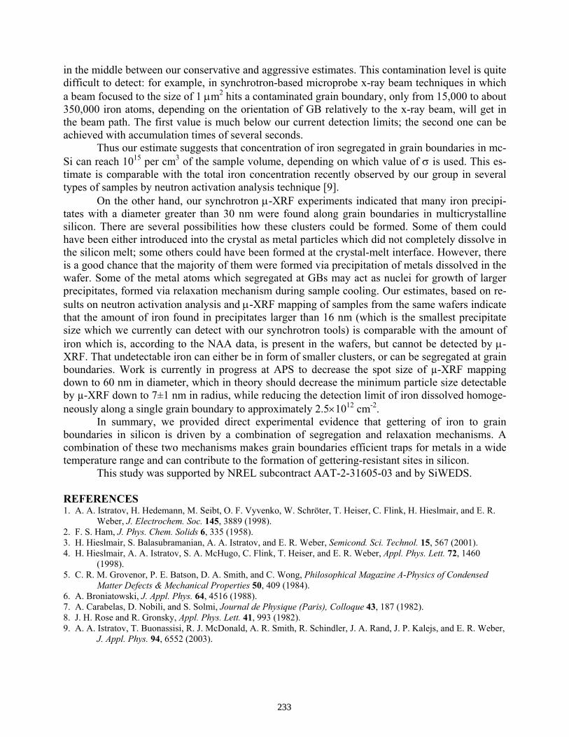
in the middle between our conservative and aggressive estimates. This contamination level is quite difficult to detect: for example, in synchrotron-based microprobe x-ray beam techniques in which a beam focused to the size of 1 µm2 hits a contaminated grain boundary, only from 15,000 to about 350,000 iron atoms, depending on the orientation of GB relatively to the x-ray beam, will get in the beam path. The first value is much below our current detection limits; the second one can be achieved with accumulation times of several seconds.
Thus our estimate suggests that concentration of iron segregated in grain boundaries in mc-Si can reach 1015 per cm3 of the sample volume, depending on which value of σ is used. This es-timate is comparable with the total iron concentration recently observed by our group in several types of samples by neutron activation analysis technique [9].
On the other hand, our synchrotron µ-XRF experiments indicated that many iron precipi-tates with a diameter greater than 30 nm were found along grain boundaries in multicrystalline silicon. There are several possibilities how these clusters could be formed. Some of them could have been either introduced into the crystal as metal particles which did not completely dissolve in the silicon melt; some others could have been formed at the crystal-melt interface. However, there is a good chance that the majority of them were formed via precipitation of metals dissolved in the wafer. Some of the metal atoms which segregated at GBs may act as nuclei for growth of larger precipitates, formed via relaxation mechanism during sample cooling. Our estimates, based on re-sults on neutron activation analysis and µ-XRF mapping of samples from the same wafers indicate that the amount of iron found in precipitates larger than 16 nm (which is the smallest precipitate size which we currently can detect with our synchrotron tools) is comparable with the amount of iron which is, according to the NAA data, is present in the wafers, but cannot be detected by µ-XRF. That undetectable iron can either be in form of smaller clusters, or can be segregated at grain boundaries. Work is currently in progress at APS to decrease the spot size of µ-XRF mapping down to 60 nm in diameter, which in theory should decrease the minimum particle size detectable by µ-XRF down to 7±1 nm in radius, while reducing the detection limit of iron dissolved homoge-neously along a single grain boundary to approximately 2.5×1012 cm-2.
In summary, we provided direct experimental evidence that gettering of iron to grain boundaries in silicon is driven by a combination of segregation and relaxation mechanisms. A combination of these two mechanisms makes grain boundaries efficient traps for metals in a wide temperature range and can contribute to the formation of gettering-resistant sites in silicon.
This study was supported by NREL subcontract AAT-2-31605-03 and by SiWEDS.
REFERENCES 1. A. A. Istratov, H. Hedemann, M. Seibt, O. F. Vyvenko, W. Schröter, T. Heiser, C. Flink, H. Hieslmair, and E. R.
Weber, J. Electrochem. Soc. 145, 3889 (1998). 2. F. S. Ham, J. Phys. Chem. Solids 6, 335 (1958). 3. H. Hieslmair, S. Balasubramanian, A. A. Istratov, and E. R. Weber, Semicond. Sci. Technol. 15, 567 (2001). 4. H. Hieslmair, A. A. Istratov, S. A. McHugo, C. Flink, T. Heiser, and E. R. Weber, Appl. Phys. Lett. 72, 1460
(1998). 5. C. R. M. Grovenor, P. E. Batson, D. A. Smith, and C. Wong, Philosophical Magazine A-Physics of Condensed
Matter Defects & Mechanical Properties 50, 409 (1984). 6. A. Broniatowski, J. Appl. Phys. 64, 4516 (1988). 7. A. Carabelas, D. Nobili, and S. Solmi, Journal de Physique (Paris), Colloque 43, 187 (1982). 8. J. H. Rose and R. Gronsky, Appl. Phys. Lett. 41, 993 (1982). 9. A. A. Istratov, T. Buonassisi, R. J. McDonald, A. R. Smith, R. Schindler, J. A. Rand, J. P. Kalejs, and E. R. Weber,
J. Appl. Phys. 94, 6552 (2003).
233

The Commercial Status of the PV Industry in 2004 – Identifying Important and Unimportant Factors
Bolko von Roedern
NREL, NCPV, Thin Film Partnership, Golden, CO 80401-3393
This Paper reviews the current status of the commercial PV Industry. It assesses the current status of commercially available modules, most of which use silicon wafers or ribbons. My analysis will show that the choice of Si wafers or substrates, once deemed to be the most important aspect, ended up making only negligible differences for commercial products, as long as cells are prepared by diffusion and screen printing. I will also address the prospects and requirements for both next generation thin-film modules and super-high (>20%) efficient commercial crystalline Si cells. It is shown that traditional recombination loss analyses provide a poor tool for understanding limitations of cell and module performance, because those analytical schemes ignore dominating interactions between different loss mechanisms (e.g., of surface and bulk recombination).
1. Results used for Discussion
A survey was conducted using PV module manufacturer’s product specifications on their corporate websites. Table 1 gives the results of the survey as of May 2004. The ranking by efficiency was calculated as module power divided by total module area. Eff. (%)
Module T.coeff. (%P/oC)
comments
16.9 SunPower SPR210 na (‘low’) Rear contact cells, FZ wafers 16.1 Sanyo HIP190BA2 -0.33 “HIT”heterojunction cell, n-type CZ wafers14.2 Sharp NT-185-U1 na CZ wafers, diffused cells 13.5 BP4170 -0.5 Laser-grooved buried contacts, CZ wafers 13.1 Kyocera KC167G VOC=-0.12 Cast multi-Si wafers 13.0 RWESchott ASE-300-
DGF/315 -0.47 EFG ribbon
12.8 Sharp ND-167-U1 na Cast multi-Si wafers 12.7 BP3160 -0.5 Cast multi-Si wafers (“Solarex”) 12.1 Shell SQ160-C -0.52 CZ wafers (“semisquare, CA Siemens Solar”) 11.6 Evergreen Solar EC115 -0.4 “String ribbon” Si 11.5 GEPV-165M (up to)-0.5 Reclaimed semiconductor wafers (“AstroPower”)
11.1 Shell S115-C -0.45 Cast multi-Si wafers (German cells) 11.0 WürthSolar WS31050/80 -0.36 “CIGS” thin-film 9.4 Shell Solar ST-40 -0.6 “CIGSS” thin-film 7.6 First Solar FS55 -0.25 “CdTe” thin-film 6.4 Mitsubishi Heavy MA100 -0.2 a-Si single-junction thin-film, vhf deposition 6.3 Uni-Solar US-64 (<0.3) a-Si triple junction, rating increase to 68W
(6.7%) pending
234

For several manufacturers, the same module is available with different power
ratings. In those instances, the highest power rating was used for calculating the indicated total-area efficiencies. Also indicated are the expected power loss rates for higher than standard (25oC) operating temperatures, when provided on the module
specification sheet. The second set of data used for my analyses comes from a presentation by R. Swanson [1], which outlines a pathway towards achieving much higher crystalline Si solar cell efficiencies. His analysis provides a detailed breakdown which device manipulations or process modifications would increase the present-day “standard” average 14.7% Si solar cell efficiency to higher numbers. Table 2 summarizes
these conclusions. 2. Discussion
These 2 tables make it quite clear that for cells with diffused junctions and screen-printed contacts, “Si-quality” or lifetime has become a factor that no longer drives cell performance, even though many experimental lifetime measurements may find a correlation between measured wafer lifetimes and cell parameters. The proof of this statement also comes from the observation that today RWE-Schott can deliver 13% efficient commercial product with EFG cells, where EFG is often referred to as the lowest quality Si material (compared to CZ and cast-ingot multi-Si), while the “best” wafers (reclaimed semiconductor wafers) result in lower efficiency product for GE (‘AstroPower’). In other words, we have now been taught by commercial reality that the processing by diffusion and screen printing has become an “equalizer,” while it had been expected that Si quality (usually ranked as QFZ > QCZ > Qmulti > Qribbon) would determine the commercially achievable efficiency rates. The data in the two tables suggests that losses (i.e., less-than-ideal performance) are not simply individual factors that arithmetically subtract from some “realistic-ideal” cell efficiency value (often taken as approximately 25% for Si cells operating at 1-sun intensity). Rather it is quite evident that the losses are quite interactive. This is directly evident from the difference between lines 8 and 9 in table 2. The rankings in Table 1 make it clear that the choice of alternative junction processes (BP Solar, Sanyo, and SunPower) has been implemented with varying degree of success. While two approaches rely on ‘traditional’ concepts of geometrical contact restriction, it is quite remarkable that a “full surface” Sanyo ‘HIT’ contacting approach employing heterojunction contacts can give very high commercial solar cell performance as well. When first reported, many of those working on wafer-Si based solar cells questioned whether it would make sense to
Row Material or Device Enhancement Measure
Commercial cell eff. (%)
1 “Conventional” Silicon Cell 14.7 2 High Lifetime Base 14.8 3 Back Surface Field (BSF) 15.6 4 Rear Local Contacts (RLC) 16.5 5 Passivated Emitter (PE) 16.8 6 Selective Emitter (SE) 17.1 7 BSF + PE 18.3 8 SE + RLC 19.7 9 High Lifetime + SE + RCL 21.2
235
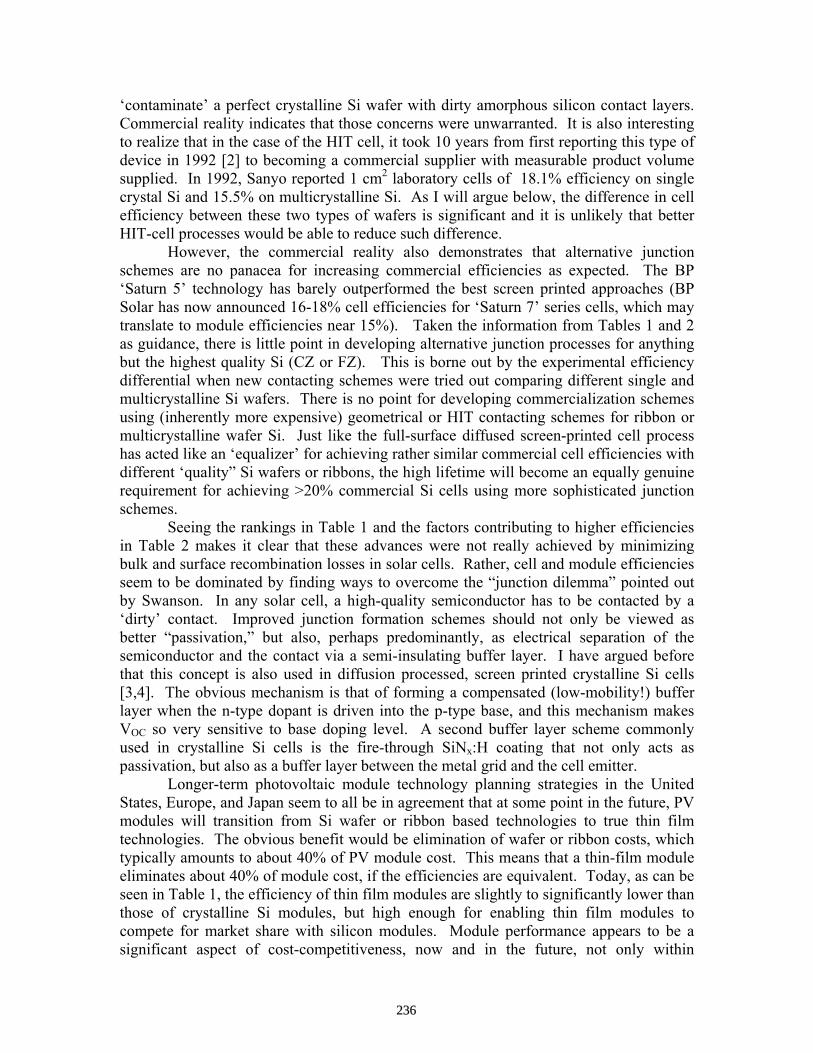
‘contaminate’ a perfect crystalline Si wafer with dirty amorphous silicon contact layers. Commercial reality indicates that those concerns were unwarranted. It is also interesting to realize that in the case of the HIT cell, it took 10 years from first reporting this type of device in 1992 [2] to becoming a commercial supplier with measurable product volume supplied. In 1992, Sanyo reported 1 cm2 laboratory cells of 18.1% efficiency on single crystal Si and 15.5% on multicrystalline Si. As I will argue below, the difference in cell efficiency between these two types of wafers is significant and it is unlikely that better HIT-cell processes would be able to reduce such difference.
However, the commercial reality also demonstrates that alternative junction schemes are no panacea for increasing commercial efficiencies as expected. The BP ‘Saturn 5’ technology has barely outperformed the best screen printed approaches (BP Solar has now announced 16-18% cell efficiencies for ‘Saturn 7’ series cells, which may translate to module efficiencies near 15%). Taken the information from Tables 1 and 2 as guidance, there is little point in developing alternative junction processes for anything but the highest quality Si (CZ or FZ). This is borne out by the experimental efficiency differential when new contacting schemes were tried out comparing different single and multicrystalline Si wafers. There is no point for developing commercialization schemes using (inherently more expensive) geometrical or HIT contacting schemes for ribbon or multicrystalline wafer Si. Just like the full-surface diffused screen-printed cell process has acted like an ‘equalizer’ for achieving rather similar commercial cell efficiencies with different ‘quality” Si wafers or ribbons, the high lifetime will become an equally genuine requirement for achieving >20% commercial Si cells using more sophisticated junction schemes.
Seeing the rankings in Table 1 and the factors contributing to higher efficiencies in Table 2 makes it clear that these advances were not really achieved by minimizing bulk and surface recombination losses in solar cells. Rather, cell and module efficiencies seem to be dominated by finding ways to overcome the “junction dilemma” pointed out by Swanson. In any solar cell, a high-quality semiconductor has to be contacted by a ‘dirty’ contact. Improved junction formation schemes should not only be viewed as better “passivation,” but also, perhaps predominantly, as electrical separation of the semiconductor and the contact via a semi-insulating buffer layer. I have argued before that this concept is also used in diffusion processed, screen printed crystalline Si cells [3,4]. The obvious mechanism is that of forming a compensated (low-mobility!) buffer layer when the n-type dopant is driven into the p-type base, and this mechanism makes VOC so very sensitive to base doping level. A second buffer layer scheme commonly used in crystalline Si cells is the fire-through SiNx:H coating that not only acts as passivation, but also as a buffer layer between the metal grid and the cell emitter.
Longer-term photovoltaic module technology planning strategies in the United States, Europe, and Japan seem to all be in agreement that at some point in the future, PV modules will transition from Si wafer or ribbon based technologies to true thin film technologies. The obvious benefit would be elimination of wafer or ribbon costs, which typically amounts to about 40% of PV module cost. This means that a thin-film module eliminates about 40% of module cost, if the efficiencies are equivalent. Today, as can be seen in Table 1, the efficiency of thin film modules are slightly to significantly lower than those of crystalline Si modules, but high enough for enabling thin film modules to compete for market share with silicon modules. Module performance appears to be a significant aspect of cost-competitiveness, now and in the future, not only within
236

crystalline Si technologies, but also for thin films. To assure competitiveness in the future, thin film PV module performance has to show as much relative efficiency progress as will be made for crystalline Si modules. Due to monolithic fabrication, there may be further manufacturing cost reductions for thin film PV modules, compared to crystalline Si that requires cell processing and string assemblies. It can also be expected that future developments will reduce the cost of the module package for both thin films and crystalline Si technologies [5]. Finally, the entire PV systems cost will change once PV is integrated into buildings, rather than being added to buildings as modules. Again, for these applications thin films possess some advantages over crystalline Si.
Thin films appear to have reached the necessary maturity to compete with crystalline Si and be available as a technology to assure further PV cost-reduction potential at the point in time when crystalline Si technology cost reductions will saturate. This can be expected to occur once Si technology becomes limited by raw materials cost, at a wafer cost of $0.42/Wp, (a silicon feedstock price of $30/kg and a projected 14kg/kWp requirement), or after 2 to 4 more doublings of today’s commercial output [6]. Contrary to some past beliefs, thin film PV is not ‘inherently cheap’ if the efficiency is too low (currently, I argue, if it is <6%). In the context of this workshop, there has always been a strong expectation that wafer (ribbon) Si PV technology would transition to thin-film Si technology. However, at present, it looks like CuInGaSe2-cells (CIGS) and CdTe modules may outperform Si thin films by a significant enough margin to give them a competitive edge. Already today, best CIGS products and some older Si module products are of equal performance [7]. Amorphous silicon performance also remains competitive, but less so than the polycrystalline thin films. Integration into roofing systems, an approach pursued by Uni-Solar, may offset the lower efficiency potential. True thin film crystalline Si PV approaches deserve further research as well; but based on today’s performance, commercialization is unlikely until better cell and module performance, and manufacturing yield, have been demonstrated [8]. References
1 R. Swanson, presented at the Material Research Society Spring Meeting, 04/2004, San Francisco, CA, Symposium A (to be published).
2 Y. Kuwano, S. Nakano, M. Tanaka, T. Takhama, T. Matsuyama, M. Isomura, N. Nakamura, H. Haku, M. Nishikuni, H. Nishiwaki, and S. Tsuda, Materials Research Society Symposia Proceedings, 258, (1992) 857.
3 B. von Roedern and G.H. Bauer, Proc. 9th Workshop on Crystalline Silicon Solar Cell Materials and Processes, Breckenridge, CO, (1999) NREL/BK-520-26941, 219.
4 B. von Roedern , Encyclopedia of Energy, Volume 5, (2004) Elsevier, Inc. 47, (see entry under “Photovoltaic Materials, Physics of”).
5 K. Zweibel, to be published at the Solar Technology Review Meeting, Denver, CO, 10/2004.
6 T. Surek, Proc. 3rd World Conf. On Photovoltaic Energy Conversion, Osaka, 05/2003, paper 8PL-E3-01.
7 J.A. delCueto, Proc. 29th IEEE PVSC, New Orleans, LA, 5/2002, p. 1523. 8 B. von Roedern, Proceedings NCPV and Solar Technology Review Meeting,
Denver, CO, 3/2003, p. 552.
237
MODELING THE GETTERING OF METALLIC PRECIPITATES WITH VOLUME MISFITS IN SILICON
Na Li, Hui Li, and Teh Y. Tan
Department of Mechanical Engineering and Materials Science
Duke University Durham, NC 27708-0300
ABSTRACT
The problem of gettering of metallic precipitates in Si, for which there exists a vol-ume misfit between the precipitate and the Si matrix material, has been formulated. The gettering process is modeled using an Al-Si liquid layer, and the volume misfit associated with dissolving the precipitates is assumed as accommodated by point defects, which may be dominated by vacancies (V), self-interstitials (I), or both contributing. The effect of point defects on gettering is demonstrated in an initial simulation result on gettering of FeSi2 (with a misfit of –0.15), which showed that the precipitate dissolution process is faster under V supersaturation.
INTRODUCTION
Gettering of dissolved and precipitated metallic contaminants is important in Si solar cell fabrication for improving the cell efficiency. Si is an indirect bandgap semiconductor, with its carrier lifetime controlled by electrically active impurities (metals) and defects. In solar cells, these impurities and defects lead to low cell efficiencies. While point defects must be present to their thermal equilibrium concentrations in Si, the presence of impurities is, however, an ex-traneous factor that can be controlled by cleaning and by gettering. We have recently devoted an effort to identify the involved physics and to accordingly model the metal electrical activity1-3 and the metal gettering processes.4-7 The latter includes metal dis-solution from the precipitates, diffusion of metal atoms to, and their stabilization at the gettering sites. In the present study, we further address the role of the precipitate volume misfit with the Si matrix and the resulting effect on the gettering process. We formulate the problem using an Al-Si liquid layer as the getterer and interstitial Fe and FeSi2 as the gettered metal and precipitates. In this problem, the misfit of the precipitate is assumed to be accommodated by the point defect species vacancies (V) and Si self-interstitials (I).
FORMULATION OF THE PROBELM Gettering of M by the Al-Si liquid involves the segregation processes taking place at the in-terface of Si and the liquid layer, which occurs simultaneously with impurity diffusion. Account-ing for M diffusion, segregation, and dissolution of the precipitates, the time change rate of M atoms is given by4,7
∂CM / ∂t = ∂ / ∂x DM ∂CM / ∂x − (CM / mM )(∂mM / ∂x)( )[ ]− (4πr2ρ / ΩMSix)(dr / dt) . (1)
238
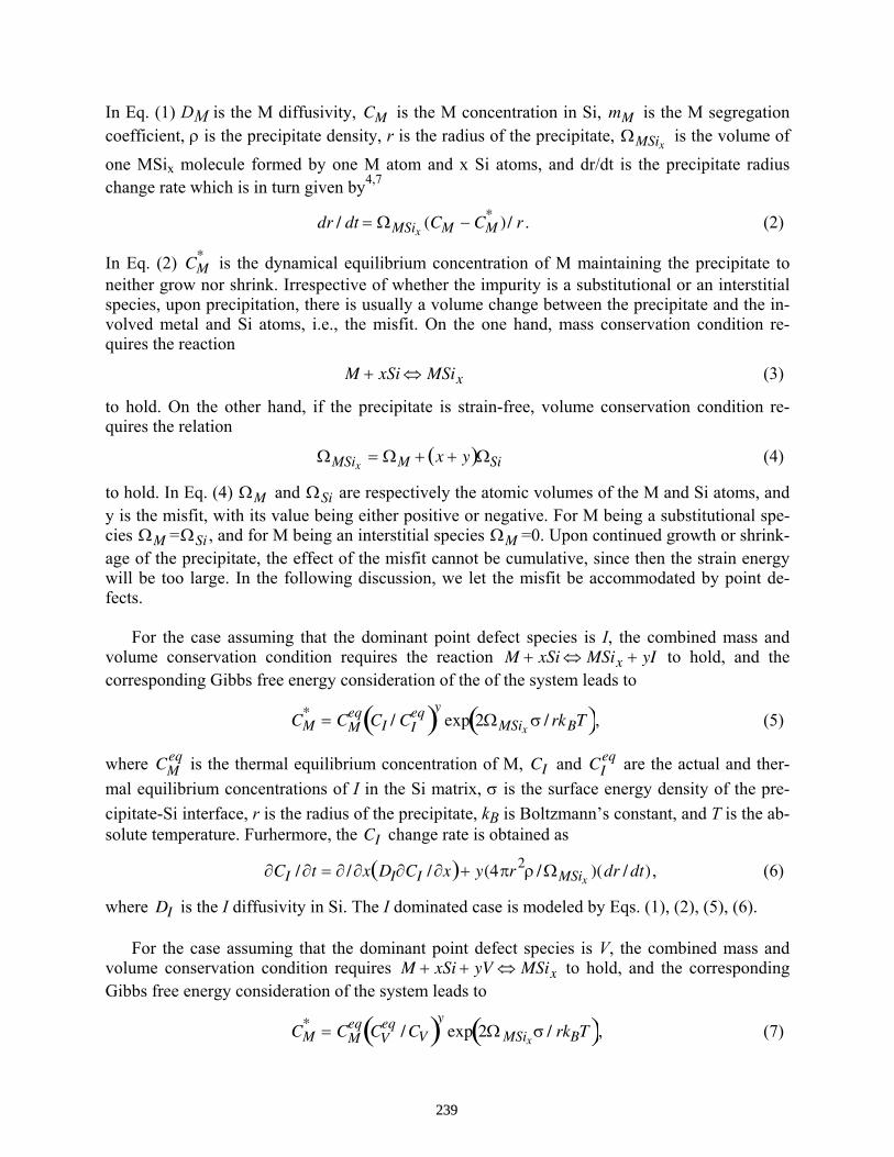
In Eq. (1) DM is the M diffusivity, CM is the M concentration in Si, mM is the M segregation coefficient, ρ is the precipitate density, r is the radius of the precipitate, ΩMSix is the volume of one MSix molecule formed by one M atom and x Si atoms, and dr/dt is the precipitate radius change rate which is in turn given by4,7
dr / dt = ΩMSix (CM − CM* )/ r . (2)
In Eq. (2) CM* is the dynamical equilibrium concentration of M maintaining the precipitate to
neither grow nor shrink. Irrespective of whether the impurity is a substitutional or an interstitial species, upon precipitation, there is usually a volume change between the precipitate and the in-volved metal and Si atoms, i.e., the misfit. On the one hand, mass conservation condition re-quires the reaction
M + xSi ⇔ MSix (3)
to hold. On the other hand, if the precipitate is strain-free, volume conservation condition re-quires the relation
ΩMSix = ΩM + x + y( )ΩSi (4)
to hold. In Eq. (4) ΩM and ΩSi are respectively the atomic volumes of the M and Si atoms, and y is the misfit, with its value being either positive or negative. For M being a substitutional spe-cies ΩM =ΩSi , and for M being an interstitial species ΩM =0. Upon continued growth or shrink-age of the precipitate, the effect of the misfit cannot be cumulative, since then the strain energy will be too large. In the following discussion, we let the misfit be accommodated by point de-fects.
For the case assuming that the dominant point defect species is I, the combined mass and volume conservation condition requires the reaction M + xSi ⇔ MSix + yI to hold, and the corresponding Gibbs free energy consideration of the of the system leads to
CM* = CM
eq CI / CIeq( )y
exp 2ΩMSix σ / rkBT( ), (5)
where CMeq is the thermal equilibrium concentration of M, CI and CI
eq are the actual and ther-mal equilibrium concentrations of I in the Si matrix, σ is the surface energy density of the pre-cipitate-Si interface, r is the radius of the precipitate, kB is Boltzmann’s constant, and T is the ab-solute temperature. Furhermore, the CI change rate is obtained as
∂CI / ∂t = ∂ / ∂x DI∂CI / ∂x( )+ y(4πr2ρ / ΩMSix )(dr / dt) , (6)
where DI is the I diffusivity in Si. The I dominated case is modeled by Eqs. (1), (2), (5), (6).
For the case assuming that the dominant point defect species is V, the combined mass and volume conservation condition requires M + xSi + yV ⇔ MSix to hold, and the corresponding Gibbs free energy consideration of the system leads to
CM* = CM
eq CVeq / CV( )y
exp 2Ω MSix σ / rkBT( ), (7)
239

where CV and CVeq are the actual and thermal equilibrium concentrations of V in the Si matrix.
Furthermore, the CV change rate is obtained as ∂CV / ∂t = ∂ / ∂x DV∂CV / ∂x( )− y(4πr2ρ / ΩMSix )(dr / dt) , (8)
where DV is the V diffusivity in Si. The V dominated case is modeled by Eqs. (1), (2), (7), (8). The most accurate approach is to assume that both I and V contribute to the relieve of the misfit, for which the combined mass and volume conservation condition requires the reaction M + xSi + zyV ⇔ MSix + (1 − z )yI to hold. In this reaction z (with a value less than 1) is the fractional contribution of V to the relief of the misfit and (1-z) is the fractional I contribution. I and V will interact via the reaction I + V ⇔ φ , where φ is a Si lattice atom. Accordingly, it can be assumed that the I-V dynamical equilibrium condition CICV = CI
eqCVeq has been fulfilled.
With these conditions, the corresponding Gibbs free energy considertion of the system leads to
CM* = CM
eq CI / CIeq( )y
exp 2ΩMSix σ / rkBT( )= CMeq CV
eq / CV( )y exp 2ΩMSix σ / rkBT( ). (9)
The I and V time change rates are obtained as
∂CI / ∂t = ∂ / ∂x DI∂CI / ∂x( )+ (1− z)y(4πr2ρ / ΩMSix )(dr / dt) , (10)
∂CV / ∂t = ∂ / ∂x DV∂CV / ∂x( )− zy(4πr2ρ / ΩMSix )(dr / dt) . (11)
Furhtermore, the factor z, which is a function of t and x, is obtained as
z =CV
CI + CV+ CV
∂∂x
DI∂CI
∂x
+ CI
∂∂x
DV∂CV
∂x
/ yρ
4πr2
ΩMSix
CI + CV( )dr
dt
. (12)
The case is modeled using Eqs. (1), (2), and (9)-(12).
INITIAL NUMERICAL SIMULATION RESULTS As an initial test of the soundness of the model, numerical simulations were carried out for gettering Fe in Si wafers 200 µm in thickness by a 2 µm thick Al-Si liquid layer at the wafer backsurface (at the 200 µm position). It is assumed that Fe was introduced at 900oC to its solu-bility of ~4.3x1013 cm-3 and then precipitated out to steady state at 700oC to the density of =1011 cm-3. For the interstitial Fe atoms ΩM =0 and for the FeSi2 precipitates ΩMSix =1.85ΩSi ,
8 and hence y=-0.15 obtains from Eq. (2). The negative y value means that growth of FeSi2 precipitates is associated with a volume contraction while their dissolution with a volume expansion. Thus, generation of V or consumption of I or both will result from FeSi2 precipitate growth, while generation of I or consumption of V or both will result from FeSi2 precipitate dis-solution. Consequently, gettering will be faster if a V-supersaturation exist. Figure 1 shows two hypothetical cases for which CV =10CV
eq holds for case (a) and CV =CVeq for case (b), and it is
clear that gettering in case (a) is much more effective becasue of the V supersaturation. Simula-tions of more realistic cases are in progress.
240
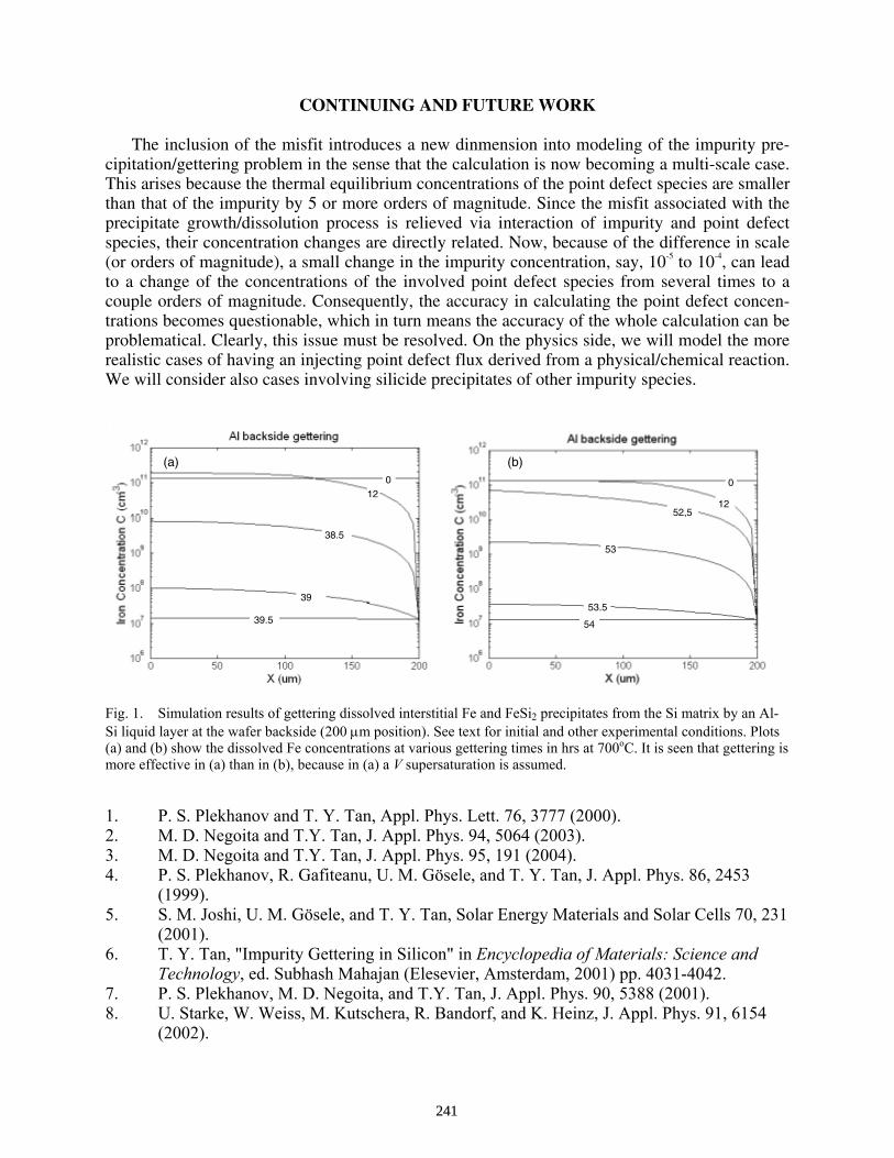
CONTINUING AND FUTURE WORK The inclusion of the misfit introduces a new dinmension into modeling of the impurity pre-cipitation/gettering problem in the sense that the calculation is now becoming a multi-scale case. This arises because the thermal equilibrium concentrations of the point defect species are smaller than that of the impurity by 5 or more orders of magnitude. Since the misfit associated with the precipitate growth/dissolution process is relieved via interaction of impurity and point defect species, their concentration changes are directly related. Now, because of the difference in scale (or orders of magnitude), a small change in the impurity concentration, say, 10-5 to 10-4, can lead to a change of the concentrations of the involved point defect species from several times to a couple orders of magnitude. Consequently, the accuracy in calculating the point defect concen-trations becomes questionable, which in turn means the accuracy of the whole calculation can be problematical. Clearly, this issue must be resolved. On the physics side, we will model the more realistic cases of having an injecting point defect flux derived from a physical/chemical reaction. We will consider also cases involving silicide precipitates of other impurity species.
0
1252,5
53
53.5
54
012
38.5
39
39.5
(a) (b)
Fig. 1. Simulation results of gettering dissolved interstitial Fe and FeSi2 precipitates from the Si matrix by an Al-Si liquid layer at the wafer backside (200 µm position). See text for initial and other experimental conditions. Plots (a) and (b) show the dissolved Fe concentrations at various gettering times in hrs at 700oC. It is seen that gettering is more effective in (a) than in (b), because in (a) a V supersaturation is assumed. 1. P. S. Plekhanov and T. Y. Tan, Appl. Phys. Lett. 76, 3777 (2000). 2. M. D. Negoita and T.Y. Tan, J. Appl. Phys. 94, 5064 (2003). 3. M. D. Negoita and T.Y. Tan, J. Appl. Phys. 95, 191 (2004). 4. P. S. Plekhanov, R. Gafiteanu, U. M. Gösele, and T. Y. Tan, J. Appl. Phys. 86, 2453
(1999). 5. S. M. Joshi, U. M. Gösele, and T. Y. Tan, Solar Energy Materials and Solar Cells 70, 231
(2001). 6. T. Y. Tan, "Impurity Gettering in Silicon" in Encyclopedia of Materials: Science and
Technology, ed. Subhash Mahajan (Elesevier, Amsterdam, 2001) pp. 4031-4042. 7. P. S. Plekhanov, M. D. Negoita, and T.Y. Tan, J. Appl. Phys. 90, 5388 (2001). 8. U. Starke, W. Weiss, M. Kutschera, R. Bandorf, and K. Heinz, J. Appl. Phys. 91, 6154
(2002).
241

Carbon precipitation in polycrystalline ribbon silicon: impact of oxygen content and thermal cycling
Jinggang Lu1, George Rozgonyi1, Axel Schönecker2, Astrid Gutjahr2, and Zhenxian Liu3
1Materials Science and Engineering Department, North Carolina State University, Raleigh, NC 27695-7916 2Energy Research Center of the Netherlands, ECN, POBox 1, NL-1755 ZG Petten, Netherlands
3National Synchrotron Light Source, Brookhaven National Laboratory, Upton, NY 11973 a) Email: [email protected]
ABSTRACT:
The behavior of carbon precipitation in relation to oxygen content in polycrystalline RGS (Ribbon Growth on Substrate) ribbon silicon subject to various heat treatments has been investigated by infrared spectroscopy. It is found that carbon precipitation in high oxygen wafers consists of two distinct steps; namely, an initial rapid carbon reduction/oxygen precipitation phase in the first hour annealing, followed by slow precipitation during a subsequent prolonged annealing. The first step is likely controlled by the formation of high diffusivity interstitial carbon, due to silicon self-interstitial generation during oxygen precipitation; whereas the slow precipitation step is controlled by substitutional carbon diffusion, and is strongly dependent on the annealing temperature. A higher oxygen content was found to enhance carbon precipitation throughout the two steps, probably by generating more self-interstitials and by providing heterogeneous nucleation sites for carbon precipitation. I. INTRODUCTION
Substitutional carbon (CS) in crystalline silicon is not electrical active1. Studies of carbon in Czochralski silicon have mainly focused on its enhancement effect on oxygen precipitation2-6 and interactions with silicon self-interstitials (ISi)7-8. Carbon precipitation by itself is rarely an important process because of the typically low CS levels in silicon wafers9. The situation is very different in polycrystalline ribbon silicon, which usually contains a high concentration of CS, ranging from 0.5 to 2 x 1018 cm-3. The high degree of carbon supersaturation and the presence of interstitial oxygen (Oi) enhance the formation of carbon precipitates. A high density of carbon precipitates will degrade the minority carrier lifetime by introducing interfacial states into the energy bandgap. Thus, detailed knowledge on carbon precipitation, especially regarding to the impact of oxygen content, is required to improve the performance of solar cells made from these high carbon content ribbon silicon. In this letter, the behavior of carbon precipitation in relation to oxygen content in polycrystalline ribbon silicon is investigated by infrared spectroscopy.
II. EXPERIMENT
Four sets of RGS silicon ribbons10 with similar carbon concentration and very different oxygen content, denoted as # 92, 133, 149, and 226, respectively, were grown at the Energy Research Center of the Netherlands. The variation in Cs concentration between different 1x1 cm2 size samples cut from the same wafer usually varies from 1 to 2 x 1017 cm-3. Such a large variation prevents us from using large samples to examine small changes in Cs concentration. Thus, to minimize this sample-to-sample variation, small 2 x 2.5 mm2 pieces were cut from the 1 x 1 cm2 samples and annealed in nitrogen at 800, 900, and 10200C for different times. The annealed samples were then dipped in a dilute HF solution to remove the oxide layer, and examined on a Bruker 66v/S Fourier transform infrared spectrometer equipped with a IR microscope at the U2A beamline of the National Synchrotron Light Source of the Brookhaven National Laboratory. With the aperture of the IR microscope fully opened, the measured area was ~ 100x100 µm2 , which is determined by the beam size of the synchrotron light. A low oxygen content float-zone silicon wafer was used as a reference to subtract the silicon lattice absorption. The concentrations of Cs and Oi were determined from the absorption peaks at 607 and 1107 cm-1 using the conversion
Table I. Cs and Oi concentrations in the as-grown RGS ribbon silicon wafers.
Sample # Oi (x 1018 cm-3) Cs (x 1018 cm-3) 92 1.6 1.4 149 1.0 1.5 133 0.7 1.4 226 0.6 1.3
242

constants in ASTM methods F1391 and F1188 11, respectively. Table I summarizes the concentrations of CS and Oi in the as-grown samples. Note that samples #92, 133 and 149 have essentially same carbon content. III. RESULTS AND DISCUSSION
Figures 1s (a) and (b) show a series of representative IR absorption spectra of samples # 92 and 133 after different thermal annealing. Note that, while the two set of samples have similar carbon contents, sample #92 has a significantly higher oxygen content than sample #133. It is evident that both oxygen and carbon precipitations proceed faster in sample #92 than in sample #133. Figure 1 (a) shows that essentially all the Oi in sample #92 has precipitated within one hour at both 8000C and 9000C; whereas a noticeable Oi absorption peak is still present in the corresponding 1h annealed sample #133, see Fig. 1(b). While the fast O precipitation in the high oxygen containing sample #92 indicates that the Oi supersaturation degree is a key factor effecting oxide nucleation, it is also recognized that RGS silicon ribbons are highly defective with readily available nucleation sites for oxygen precipitation. Compared with oxygen precipitation, carbon precipitation is a relatively slow process when annealed at 9000C or below, see Fig. 1. However, when annealed at 10200C, carbon precipitation proceeds much faster, especially in the presence of a high concentration of oxygen. The faster carbon precipitation in the high Oi containing sample clearly suggests an enhancement effect of Oi on carbon precipitation. We note that oxygen content also has an impact on the shape of the SiC IR absorption bands located at 800-930 cm-1. This will be addressed in a separated paper12.
Fig. 1. FTIR spectra of samples #92 and 133 after different annealing procedures. Spectra are shifted for clarity.
The reduction of Oi and Cs in samples #92 during single step annealing performed at 800 and 900oC is shown in Figs. 2 (a) and (b), respectively. It is evident from Fig. 2 (a) that, with essentially all the Oi precipitate during the 1h annealing at 8000C, the Cs concentration only decreased by 30% from 14 to 10 x 1017 cm-3. Note that the opposite volume change associated with oxygen (+) and carbon (-) precipitation favors co-precipitation in an approximate ratio of 2:1, as observed in Czochralski silicon3. In sample # 92, the measured co-precipitation ratio of oxygen and carbon is approximately 4:1. The reduced carbon precipitation is likely due to absorption of Si self-interstitials (ISi) by grain boundaries and dislocations. It is known that silicon self-interstitials are generated during oxygen precipitation, and interstitial carbon can therefore form through a capture of ISi by Cs atoms. The high diffusivity of interstitial carbon allows it to readily precipitate or form complexes with oxygen. Since grain boundaries and dislocations can act as effective sinks for ISi and considering that one ISi is emitted for every two precipitated oxygen atom, a co-precipitation ratio of 4:1 simply implies that approximately half of the ISi generated during oxygen precipitation are trapped by Cs atoms, and the other half are absorbed by other sinks, such as grain boundaries or dislocations. Also note from Fig. 2 (a) that there is no further carbon precipitation during a prolonged annealing after the rapid precipitation in the very first hour. Evidently, without the assistance of ISi, carbon precipitation cannot proceed at such a low temperature due to the small diffusivity of Cs.
The carbon precipitation behavior in sample #92 in the early stage of 9000C annealing is similar to that at 8000C. After the initial fast precipitation, Cs continued to precipitate during prolonged 9000C annealing, and its concentration reached 4.7 x 1017 cm-3 after 64h, see Fig. 2 (b). Since the annealing was performed under nitrogen
243
0
3
6
9
12
15
18
0 1 2 4 8 32 64Annealing time (h)
conc
entra
tion
(x10
17 c
m -3
)CsOi
(a) #92-8000C
0
3
6
9
12
15
18
0 1 2 4 8 16 32 48 64Annealing time (h)
conc
entra
tion
(x10
17 c
m -3
)
CsOi
(b) #92-9000C
Fig. 2. Oi and Cs concentrations in samples #92 annealed at 800 oC (a) and 900oC (b) for different times.
0
3
6
9
12
15
18
0 1 2 4 8 32 64Annealing time (h)
conc
entra
tion
(x10
17 c
m -3
)
CsOi
(a) #133-8000C
0
3
6
9
12
15
18
0 1 2 4 8 16 32 48 64Annealing time (h)
conc
entra
tion
(x10
17 c
m -3
)
CsOi
(b) #133-9000C
Fig. 3. Oi and Cs concentrations in samples #133 annealed at 800 oC (a) and 900oC (b) for different times.
ambient and all the Oi precipitated in the first hour annealing, there will be no ISi injection during subsequent annealing. Thus, carbon precipitation can only proceed via diffusion of substitutional carbon, which is obviously higher at 9000C. Note that carbon precipitation in the high oxygen containing wafers consists of two distinct steps, namely, a fast precipitation in the very first hour of annealing, followed by slow precipitation during prolonged annealing. The first step is controlled by the formation of interstitial carbon, therefore is related to the oxygen precipitation; whereas the second step is controlled by the diffusion of substitutional carbon.
The reduced Oi supersaturation in sample #133 results in a relatively slow oxygen precipitation, see Fig. 3. Note that it takes approximately 8 hours for all the Oi to precipitate at 8000C and 9000C, considerably longer than for sample #92. Accompanying the Oi precipitation, Cs decreased from 14 to 12 x 1017 cm-3, and no further precipitation occurred after an additional 32 h annealing at 8000C, see Fig. 3 (a). The large sample-to-sample variations observed in the 9000C annealed samples prevented us from detecting the small Cs reduction (~ 1 to 2 x 1017 cm-3) accompanying the oxygen precipitation in the first 8 hours annealing, see Fig 3 (b). However, carbon reduction during the prolonged annealing process is well resolved. Note that Cs continuously precipitated during the prolonged 9000C annealing, and reached ~9 x 1017 cm-3 after 64h annealing.
The impact of oxygen content on carbon precipitation is best illustrated by comparing sample #133 and 92.
Figures 2 (a) and 3 (a) show that the annihilation of 1.6 Fig. 4. Cs concentration in 1020oC annealed samples.
244

and 0.7 x 1018 cm-3 of Oi is accompanied by a Cs concentration decrease of 4 and 2 x 1017 cm-3 in sample #92 and 133, respectively. Since the fast carbon precipitation step is likely controlled by the formation of interstitial carbon via the generation of ISi during oxygen precipitation, a slow and less aggressive oxygen precipitation in the low oxygen containing sample results in a slow and less aggressive reduction of Cs. Following the fast reduction, the Cs concentration continuously decreases during a prolonged annealing at 9000C. It is evident from Figs. 2 (b) and 3 (b) that carbon precipitation after the completion of oxygen precipitation also proceeds faster in the high oxygen containing sample. The correlation between oxygen contents and carbon precipitation rates was also observed in the 10200C annealing process, see Fig. 4. Note that the higher the Oi content, the faster the carbon precipitation. Since it took around 30 minutes to heat the samples from 900 to 10200C, oxygen precipitation is likely to have been completed during the heating up period, considering the fast precipitation observed at 800 and 9000C. As a result, carbon precipitation at 10200C (except in the very early period) is mainly controlled by Cs diffusion.
According to the theory of Ham13 on diffusion limited precipitation, the precipitation rate will be proportional to nD, where n is the precipitate density and D the diameter of the precipitates. For the same volume of SiC precipitates, nD will be larger, or the precipitation rate will be higher, if the precipitate density n is larger. A higher oxygen content can enhance SiC nucleation by providing heterogeneous nucleation sites through various C-O complexes14, as well as the oxide-silicon interface. The nucleation rate can also be enhanced with the presence of ISi generated during oxygen precipitation, considering SiC nucleation is associated with a large volume decrease producing tensile strain1, which can be relieved by ISi absorption. Thus, the enhanced carbon precipitation observed in the high Oi containing samples during annealing beyond the very first hour is likely related to the enhancement effect of oxygen on SiC nucleation. Another possible mechanism for the enhanced carbon precipitation is that co-aggregation of carbon and oxygen, as observed by SIMS measurements15, gives rise to larger precipitates, which can further result in a higher precipitation rate.
IV. CONCLUSION
In summary, carbon precipitation in four sets of polycrystalline RGS wafers, which have similar carbon content and very different oxygen concentrations, has been studied by infrared absorption spectroscopy. It is found that carbon precipitation in the high oxygen containing wafers consists two distinct steps; namely, a fast Cs reduction accompanied by oxygen precipitation in the very first hour annealing, followed by slow carbon precipitation during a prolonged annealing. The first step is likely related to the formation of high diffusivity interstitial carbon, which is controlled by ISi generation during oxygen precipitation. The slow precipitation step is controlled by Cs diffusion, and is therefore related to the annealing temperature. It is also found that a higher oxygen content enhances carbon precipitation throughout the two steps, by generating more ISi and by providing heterogeneous nucleation sites for carbon precipitation.
Reference: 1. G. Davies and R. C. Newman, in Handbook on Semiconductors, Vol. 3, 2nd ed., edited by S. Mahajan
(North-Holland, Amsterdam, 1994), p. 1557. 2. F. Shimura, J. Appl. Phys. 59, 3251 (1986). 3. Q. Sun, K. H. Yao, J. Lagowski, and H. C. Gatos, J. Appl. Phys. 67, 4313 (1990). 4. S. Hahn, M. Arst, K. N. Ritz, S. Shatas, H. J. Stein, Z. U. Rek, and W. A. Tiller, J. Appl. Phys. 64, 849 (1988). 5. P. Liu, X. Ma, J. Zhang, L. Li, and D. Que, J. Appl. Phys. 87, 3669 (2000). 6. J.-Y. Huh, U. Giisele, and T. Y. Tan, J. Appl. Phys. 78, 5926 (1995). 7. M. S. Carroll, C.-L. Chang, J. C. Sturm, and T. Buyuklimanli, Appl. Phys. Lett. 73, 3695 (1998). 8. P. A. Stolk, D. J. Eaglesham, H.-J. Gossmann, and J. M. Poate, Appl. Phys. Lett. 66, 1370 (1995). 9. W. J. Taylor, T. Y. Tan, and U. Gusele, Appl. Phys. Lett. 62, 3336 (1993). 10. H. Lange, I.A. Schwirtlich, J. Crystal Growth 104, 108 (1990). 11. Annual Book of ASTM Standards (American Society for Testing and Materials), Philadelphia, PA, 1994, Vol.
10.05, p. F1188 and F1391. 12. J. Lu, G. Rozgonyi, A. Schönecker, and A. Gutjahr, “Infrared absorption of SiC precipitates in crystalline silicon:
experimental data and theoretical interpretation”, (unpublished). 13. F. S. Ham, J. Phys. Chem. Solids 6, 335 (1958). 14. R. C. Newman and R. S. Smith, J. Phys. Chem. Solids 30, 1493 (1969). 15. F. Shimura, R. S. Hockett, D. A. Reed, and D. H. Wayne, Appl. Phys. Lett. 47, 794 (1985).
245
Progress in Silicon Heterojunction Devices by Hot-Wire CVD
M.R. Page1, E. Iwaniczko1, Q. Wang1, D.H. Levi1, Y. Yan1, H.M. Branz1, V. Yelundur2, A. Rohatgi2, and T.H. Wang1
1 National Renewable Energy Laboratory, 1617 Cole Blvd., Golden, CO 80401, USA 2 Georgia Institute of Technology, 777 Atlantic Dr., Atlanta, GA 30332, USA
ABSTRACT
We report on fabrication of silicon heterojunction (SHJ) solar cells based on Al-backed
p-type silicon wafers, with hot-wire chemical vapor deposition (HWCVD) hydrogenated amorphous silicon (a-Si:H) emitter layers. The two-layer emitters are comprised of an extremely thin (~5-nm) intrinsic a-Si:H (a-Si:H(i)) layer topped with a slightly thicker phosphorous-doped a-Si:H layer (a-Si:H(n)). Open-circuit voltages (Voc) above 620 mV are routinely achieved with a maximum of over 640 mV, indicating effective passivation of the crystalline silicon (c-Si) surface by the thin a-Si:H(i/n) stack. We used real-time spectroscopic ellipsometry (RTSE) as an in-situ diagnostic tool to monitor film thickness and roughness in real-time and to observe silicon crystallinity by further ex-situ data analysis. The deposited films were also examined by high-resolution transmission electron microscopy (HRTEM). Immediate a-Si:H deposition and a flat interface to the c-Si is the key factor in obtaining high Voc. On commercial p-type B-doped Czochralski silicon (CZ-Si) wafers with a polished surface and 2.1 Ω·cm resistivity, the best efficiency obtained is 14.8%. Efficiency above 15.7% is achieved on a 1.3 Ω·cm, p-type B-doped float-zone silicon (FZ-Si) wafer with a chemically polished front surface and a screen-printed Al-BSF.
1. INTRODUCTION
Although plasma-enhanced chemical vapor deposition (PECVD) is the dominant method for heterojunction silicon solar cell fabrication, HWCVD may have simpler reactor design and control, higher deposition rates, reduced ion bombardment of the base wafer, and atomic hydrogen (H) generation, which can be used for in-situ surface treatment and may passivate the c-Si. Furthermore, knowledge learned from the development of HWCVD heterojunction solar cells will advance our understanding of the a-Si/c-Si heterointerface.
The most important step in SHJ device development is to determine the optimum
deposition condition for a-Si:H(i) and a-Si:H(n) layers to obtain immediate a-Si:H deposition with an abrupt interface to c-Si with good conformal coverage, no epitaxy, and insensitivity to c-Si substrate orientation. With RTSE and HRTEM as the in-situ and ex-situ characterization tools, it was found that, under the conditions at which a good a-Si:H film is deposited on a glass substrate, epitaxial growth on a clean c-Si substrate is usually obtained [1]. The extent of epitaxial growth is larger as substrate temperature gets higher or with a (100)-oriented wafer. Similar deposition ambiguities have also been reported by E. Centurioni [2]. Partial epitaxy is especially difficult to avoid with HWCVD. This is undesirable because it roughens the a-Si/c-Si interface and increases the interface area and may increase the total number of interface defects. Worse yet, if part of the epitaxy reaches the doped a-Si:H region, the much higher density of trap states in doped a-Si:H (compared to those in a-Si:H(i)) will provide tunneling recombination centers for photo-generated electrons and degrade the solar cell performance. The best interface passivation and solar cell performance is achieved by a clean and flat c-Si surface in contact with a-Si:H(i). To optimize a heterojunction solar cell’s performance, the a-Si:H(i/n) emitter thickness must be minimized so that parasitic light absorption in the emitter is reduced. Finally, the a-Si:H(i) should be as thin as possible too
246

permit photogenerated holes to tunnel through to the doped a-Si:H(n) layer [3]. Here we report improved device performance after carefully tailoring growth conditions to obtain abrupt a-Si:H growth for truly heterojunction c-Si devices.
2. EXPERIMENTAL
Fig. 1 shows a schematic of our SHJ device structure. The pre-cleaned medium quality, commercial p-type B-doped CZ-Si wafers used in our device development have a polished front surface and a damage-removed back surface. We have studied a wafer resistivity range from 0.4 to 3 Ω·cm. These wafers are diamond scribed and cleaved into 25-cm by 50-cm substrates that fit into our HWCVD chamber. They are then subjected to a stringent cleaning procedure including degreasing in trichloroethylene, acetone, isopropyl alcohol, and methanol followed by drying with N2 gas. This is followed by 1) an immediate 10-min soak in boiling de-ionized (DI) water (90 MΩ·cm), 2) a 1-min DI water cascade rinse, 3) a 1% by volume hydrofluoric acid (HF) dip for 1-min or until the c-Si surface turns hydrophobic, 4) a 1-min DI water cascade rinse, and 5) drying with N2 gas. We then deposit 800-nm of aluminum at 2-nm/s by electron beam evaporation at room temperature on the back surface and alloy this back contact in a quartz tube furnace at 600°C for 20-min in 99.999% pure (5-N) forming gas (10% H2 + 90% N2). This Al-based back contact is capable of achieving 80% fill-factor and Voc exceeding 640 mV. Chemically polished 1.3 Ω·cm p-type B-doped FZ-Si wafers are cleaved into the same size as the CZ-Si substrates, screen-printed with Al paste and fired at a peak temperature around 750°C for a few minutes at Georgia Tech. At NREL the same top surface cleaning protocol is performed before HWCVD emitter deposition.
Deposition of the heterojunction emitter a-Si:H(i/n) stack (Fig. 1)
is performed by HWCVD with a tungsten filament at ~1800°C . A brief rinse of the front surface with 5-vol.% HF is employed prior to loading substrates onto the HWCVD sample platen and into the chamber load lock maintained at 1x10⁻⁶ Torr. NREL’s System-T HWCVD chamber is equipped with optical access ports for RTSE at a 70° angle of incidence. A typical deposition consists of a brief 10-sec atomic H surface treatment at 60-mTorr with 80-sccm H2 gas flow at 100-150°C substrate temperature, followed by 10-sec (5-nm) a-Si:H(i) deposition at 100-150°C and 20-sccm silane gas (SiH4) flow at 10 mTorr. The 5 to 20-nm a-Si:H(n) layer is deposited using SiH4, phosphine (PH3), and H2 gases at 100-300°C substrate temperature and 2.5-sccm, 3-sccm, 50-sccm gas flows respectively. The entire deposition process is continuously monitored by RTSE for in-situ film thickness and surface roughness feedback and for post-deposition analysis of material properties [4].
With a completed emitter, we then deposit of 80-nm of indium-tin-oxide (ITO) as the front
contact and single-layer anti-reflection coating (ARC). The ITO is deposited by thermal evaporation in an oxygen ambient at a substrate temperature of 170°C, from a 5-N purity indium-tin (90% In + 10% Sn) source in a boron nitride crucible at 900°C. This step is also believed to activate the dopants for a-Si:H(n) layers that are deposited at low temperatures (100-150°C). We then deposit the metal (50-nm Ti/60-nm Pd/2-µm Ag/50-nm Au) front grid over the surface of the ITO using a physical shadow mask with 4% grid shadow loss over the 1-cm2 cell area. A photolithographically defined mesa is used to mask the grid and ITO for device isolation. The ITO is etched using 57-wt. % hydriodic acid in DI water [5] for 5 to 15-min at room temperature. The a-Si:H(i/n) heterojunction emitter is then etched using
Al
p / B c - S i ( 1 0 0) or (111) CZ or FZ
200 - 400
Al Alloy
80-nm ITO
5-20-nm a-Si:H(n)~5-nm a-Si:H(i)
Ti/Pd/Ag/Au
µ m
Fig. 1 Schematic of hetero-junction solar cell structure.
247

reactive ion etching at 20W 13.5-MHz radio-frequency power for 2-min in a sulfur hexafluoride (SF6) plasma at 130 mTorr.
Illuminated current-voltage characteristics (I-V) of a finished solar cell were measured by a
calibrated XT-10 solar simulator maintained by NREL’s Measurements and Characterization Division. The simulator was adjusted to approximate AM1.5 direct spectrum current using a primary c-Si reference cell certified in accordance with the world photovoltaic scale.
Internal quantum efficiency (IQE) is measured by combining global reflectance data taken
on a Varian Cary 5G UV-Vis-NIR Spectrophotometer and external quantum efficiency (EQE) measured on a grating spectral response system also maintained by NREL’s Measurements and Characterization Division. All light sources of the EQE system are filtered and a chopped triple grating monochromator (Acton Research Corporation, SpectraPro-300i) is used to produce the desired narrow spectral bands.
3. RESULTS AND DISCUSSIONS 3.1 AM1.5 J-V Results
Solar cell efficiencies of 15.7% and 14.8% have been achieved on high quality FZ-Si and lower quality CZ-Si respectively as shown in Fig. 2. From the I-V curves of Fig. 2 it is apparent that the Voc for CZ-Si is lower, most likely due to the higher resistivity of 2.1 Ω·cm. This CZ-Si has a minority carrier diffusion length (Le) of 230-µm and is slightly higher quality than the 1.0 and 0.4 Ω·cm CZ-Si Le <100-µm we used in earlier studies [1]. An efficiency of 15.7% has been achieved on the high quality 1.3 Ω·cm p-type FZ-Si with a screen-printed Al-BSF. We believe this is the highest reported efficiency for a SHJ solar cell produced by HWCVD. On 1 Ω·cm material a Voc of 628 mV is the highest we have achieved by HWCVD and the highest short-circuit current (Jsc) we have achieved is 31.8 mA/cm2 without employing the high efficiency features like double ARC or texturing. The fill-factor (FF) is 78.8% but reducing the series resistance of the a-Si:H(n)/ITO interface may improve the FF further. 3.2 IQE Results
FZ-Si is typically much higher quality material, which results in much higher FZ-Si cell IQE response than is obtained with the CZ-Si device (Fig. 3). The largest difference between these two devices is the Le as calculated from the red spectral response [6]. The longer Le for the FZ-Si material indicates that it is of much higher quality than the CZ-Si. The fact that the Le (1100-µm) is so much longer than the FZ-Si thickness (250-um) indicates a strong contribution from the Al-BSF. Surprisingly, the good red response of the FZ-Si device did not translate into appreciably higher current than in the CZ-Si device. From the global reflectance curves (Fig. 3) there is >5% reflectance loss even at the minimum in the FZ-Si compared to <1% loss at the minimum reflectance for the CZ-Si device. The efficiency for
-35
-25
-15
-5
0 0.1 0.2 0.3 0.4 0.5 0.6 0.7Voltage Bias (V)
Cur
rent
(mA
/cm
2 )
2.1 Ω-cm CZ-Si <111>Voc = 600 mVJsc = 31.4 mA/cm 2
FF = 78.5 % Le = 230 µmEfficiency = 14.8 %
1.3 Ω-cm FZ-Si <100>Voc = 628 mVJsc = 31.8 mA/cm 2
FF = 78.8 % Le = 1100 µmEfficiency = 15.7 %
Fig. 2 AM1.5 J-V curve for high efficiency HWCVD SHJ
devices on polished p-type B-doped CZ and FZ silicon.
248

the FZ-Si device would be even better had the ITO surface reflectance been as low as the CZ-Si device we suspect; more analysis of variations in ITO is necessary. Optimization of the n-layer thickness is also necessary to improve the blue response for both devices. Fig. 4 shows that the IQE response in the blue spectrum decreases as the n-layer thickness is increased from 10-nm to 30-nm due to parasitic light absorption in the n-layer. However, as the a-Si:H(n) thickness is reduced from 30-nm to 10-nm we also observed a decrease in Voc as great as 10 mV due to shunting or n-layer depletetion. Further optimization of a-Si:H(n) is needed. 4 Summary We have demonstrated SHJ solar cell conversion efficiencies of 15.7% for FZ-Si and 14.8% for CZ-Si using HWCVD-deposited a-Si:H(i/n) emitter layers on polished p-type c-Si with Al-BSF. With the addition of high efficiency features like surface texturing and double ARC to improve light trapping, these efficiencies will improve significantly. Acknowledgements
We thank Yueqin Xu, Scott Ward, Charles Teplin, and Anna Duda for their valuable technical assistance. This work is supported by U.S. DOE under Contract #DE-AC36-99G010337. References [1] T.H. Wang, Q. Wang, E. Iwaniczko, M.R. Page, D.H. Levi, Y. Yan, C.W. Teplin, Y. Xu,
X.Z. Wu, and H.M. Branz, 19th EUPVSECE, June 7-11, 2004, Paris, France [2] E. Centurioni, D. Iencinella, R. Rizzoli, C. Summonte, A. Desalvo, F. Zignani, A. Migliori,
19th EUPVSECE, June 7-11, 2004, Paris, France [3] T.H. Wang, M.R. Page, E. Iwaniczko, D.H. Levi, Y. Yan, H.M. Branz, V. Yelundur, A.
Rohatgi, G. Bunea, A. Terao, and Q. Wang, 14th Workshop on Crystalline Silicon Solar Cells & Modules: Materials and Processes, Aug. 8-11, 2004, Winter Park, Colorado, USA
[4] D.H. Levi, CW. Teplin, E. Iwaniczko, R.K. Ahrenkiel, H.M. Branz, Q. Wang, T.H. Wang, To be published in MRS Proceedings, Vol. 808, 2004
[5] G. Bradshaw and A.J. Hughes, Thin Solid Films, Vol. 33(1976) L5-L7 [6] P.A. Basore, Proceedings of the 23rd IEEE Photovoltaics Specialists Conference, May
11-14, 1993, pp. 147-157, Louisville, Kentucky, USA
0
10
20
30
40
50
60
70
80
90
100
400 500 600 700 800 900 1000 1100
Wavelength (nm)
IQE
(%)
Increasing n-Layer Thickness
Fig. 4 Plot of IQE for SHJ devices with varying n-layer thicknesses; 10-nm, 15-nm, 20-nm, and 30-nm.
0
20
40
60
80
100
400 500 600 700 800 900 1000 1100Wavelength (nm)
IQE
(%)
0
20
40
60
80
100
Glo
bal R
efle
ctan
ce (%
)2.1 Ω-cm CZ-Si <111>Voc = 600 mVJsc = 31.4 mA/cm 2
FF = 78.5 % Le = 230 µmEfficiency = 14.8 %1.3 Ω-cm FZ-Si <100>Voc = 628 mVJsc = 31.8 mA/cm 2
FF = 78.8 % Le = 1100 µm Efficiency = 15.7 %
Fig. 3 IQE and global reflectance data for high efficiency p-type B-doped FZ-Si and CZ-Si devices.
249

Comparison of Ferro 3349 and CN33-462 Front Silver Pastes for 150 mm Multicrystalline Silicon Solar Cells
D. L. Meier1, R. P. Stoehr1, S. Yamanaka1, J. Salami2, T. Pham2, and A. Shaikh2
1Solar Power Industries, 13 Airport Road, Belle Vernon, PA 15012 2Ferro Electronic Materials Systems, 1395 Aspen Way, Vista, CA 92083 Introduction
A picture is emerging of screen-printed silver firing through a silicon nitride layer to contact an n-type emitter in a conventional n+p silicon solar cell [1,2]. The key role is played by the paste’s glass frit, which often includes lead oxide as one component, as it interacts with silver, silicon nitride, and silicon. At typical process temperatures, the frit becomes molten and is able to dissolve silver (about 4% by weight). This dissolved silver is later redeposited on the silicon surface as crystallites, thereby making an integral contact layer. The glass frit is designed to consume the silicon nitride layer. The glass frit also consumes some of the silicon substrate, as silicon reduces the lead oxide component of the frit to elemental lead and forms silicon dioxide. Upon cooling, the elemental lead can precipitate out in a glass matrix. These lead precipitates are thought to act as stepping stones for current conduction from the silver crystallites on the silicon surface to the solid silver particles of the silver paste which sinter together. In this picture, it is advantageous to have a number of closely-spaced small lead precipitates in the glass matrix to facilitate the tunneling of electrons.
Kinetics of the contact formation process are known to be important. Temperature must be
high enough for the frit to consume the silicon nitride and to dissolve an appropriate amount of silver and silicon, and the temperature drop must be fast enough to allow closely-spaced lead precipitates to form to promote tunneling through the re-solidified glass. In practice, these requirements are often met by “spike firing” in a radiantly-heated belt furnace, where wafers are transported through a narrow heated zone (≈ 900°C) at a high belt speed (≈ 100 ipm). Temperatures must not be so high, or times so long, for the frit to dissolve an excessive amount of the thin n+ silicon layer with the associated loss of the n-type dopant. If this occurs, contact resistance will increase because of low surface dopant concentration, and the p-n junction may become shunted. Cooling rates must be rapid enough to promote the formation of silver crystallites on the surface of the silicon and the formation of closely-spaced lead precipitates that link these silver crystallites to the sintered network of silver particles above.
This paper deals not with the microscopic structure of the silver/silicon contact, but rather with a phenomenological comparison of two commercially available silver pastes: Ferro 3349 and Ferro CN33-462. The 3349 silver paste has been widely used as a front contact material for solar cells, while the CN333-462 paste has been engineered recently with a glass frit which aggressively consumes the silicon nitride while operating over a wide process window [3]. Front silver contacts were produced both with belt furnace firing and with firing in a rapid thermal processing (RTP) chamber for finer control of the temperature profile and gas ambient. Measurements of lighted I-V, Suns-Voc, and contact resistance maps were employed to extract cell series resistance, shunt resistance, and the process window for optimum firing. It is also noteworthy that the n+ layer was formed from a phosphorus paste. No edge clean-up was used in cell fabrication, thereby eliminating a step which is common with other diffusion methods.
250

Experimental Results The starting 150 mm square multicrystalline wafers were from Deutsche Solar, 300 µm
thick, and doped with boron to 0.5 – 2.0 Ω-cm. Saw damage was first removed in hot KOH. The front n+ layer was formed by screen printing Ferro DP99-034 phosphorus paste, followed by a belt furnace diffusion to 25 – 30 Ω/ . The wafers were coated with approximately 85 nm of silicon nitride by a low-frequency PECVD process. In the initial experiments, Ferro 3347 back silver pads were printed and dried. Ferro FX53-038 aluminum was then printed on the back and dried. Finally, the front silver contact was printed using either Ferro 3349 or Ferro CN33-462 silver paste. All screen-printed metals where then co-fired in a belt furnace.
Results are given in Table 1. Series (Rs) and shunt (Rsh) resistances were taken from the
slopes of the lighted I-V curves at Voc and Jsc, respectively. Note that the major difference between the two groups is fill factor (FF), which, in turn, is influenced primarily by series resistance. These data suggest that a lower contact resistance is achieved with CN33-462 than with 3349. Note also that the shunt resistance is acceptable, even though no edge isolation step was employed and the n+ sheet resistance is low. As an initial probing of the width of the process window, the peak co-firing temperature was increased by 20°C for a small number of cells. The average efficiency of cells made with CN33-462 paste remained unchanged, while that of cells made with 3349 paste decreased by 0.9% (absolute) because of a decrease of 0.055 in FF. Thus, preliminary indications are that CN33-462 has a wider process window than 3349. Table 1. Parameters for 150 mm multicrystalline cells fabricated using 3349 and CN33-462
front silver pastes with peak co-firing temperatures T and T+20°C.
3349 CN33-462 Solar Cell Parameters
T T+20°C T T+20°C Average of Jsc (mA/cm2) 29.4 29.7 29.6 29.8 Average of Voc (V) 0.610 0.610 0.611 0.611 Average of FF 0.740 0.685 0.765 0.766 Average of Efficiency (%) 13.3 12.4 13.8 13.9 Average of Rs (Ω-cm2) 1.80 2.55 1.43 1.43 Average of Rsh (Ω-cm2) 1060 1160 1160 1130 Maximum of Efficiency (%) 13.5 12.8 14.1 14.1 Maximum of FF 0.747 0.703 0.781 0.769 Number of Cells 8 2 12 2
A larger group of wafers was processed as above, except that front silver and back
aluminum were fired sequentially, with front silver firing following aluminum alloying. The back silver pads were printed and dried prior to aluminum printing and alloying. The n+ sheet resistance in this case was approximately 30 Ω/ . Results are given in Table 2 (Lots 040629-8 and 040629-8B). Silver firing conditions had been optimized for the 3349 paste. The same firing conditions were used for CN33-462, which were not optimized for that paste. A slight improvement in efficiency and fill factor was observed for the CN33-462 paste relative to the 3349 paste, with efficiencies up to 14.4% and fill factors up to 0.771 being achieved for CN33-462. It appears that CN33-462 offers a modest improvement over 3349, even without optimization.
251

Table 2. Parameters for 150 mm multicrystalline cells fabricated using 3349 and CN33-462 front silver pastes with sequential firing of aluminum followed by silver.
Solar Cell Parameters 3349 CN33-462 Average of Jsc (mA/cm2 ) 30.0 30.1 Average of Voc (V) 0.592 0.595 Average of FF 0.738 0.740 Average of Efficiency (%) 13.1 13.3 Average of Rs (Ω-cm2 ) 1.94 1.94 Average of Rsh (Ω-cm2 ) 1130 1220 Maximum of Efficiency (%) 14.3 14.4 Maximum of FF 0.759 0.771 Number of Cells 106 96
An effort was made to determine the process window for 3349 silver paste firing by using
a highly-controlled temperature profile obtained in an RTP unit (Modular Process Technology RTP-600S) with clean dry air (CDA) as the ambient gas to mimic the ambient in a belt furnace. Peak temperatures in the range of 685°C to 805°C, as indicated by a thermocouple in contact with the surface of the wafer being processed, were examined. The temperature profile consisted of a 7-second ramp from room temperature to the peak processing temperature (≈ 100°C/s), a hold at the peak temperature for 1 s, and an abrupt termination of the lamp power to give a rapid cooldown (≈ -40°C/s) [4]. The flow of CDA through the quartz chamber of the RTP was 1 slpm. An “ideal fill factor” was determined by the Suns-Voc technique [5] to represent the FF that would be obtained if the cell series resistance were zero. In conjunction with a measurement of the “true fill factor” from the lighted I-V curve, the series resistance of the cell can be determined by:
Rs = [(Ideal FF – True FF)/0.042] Ω-cm2 (1)
150 mm multicrystalline wafers from Deutsche Solar were processed as described above
through aluminum alloying so that only the front silver printing and firing step remained. After printing, the 3349 paste was dried in a belt furnace. The wafers were then fired in the RTP. Table 3 summarizes the results of this study. Of particular interest is the trend in series resistance for the individual cells processed.
Maps of contact resistance for the cells of Table 3, made by the CoReScan instrument [6], are consistent with the values of series resistance inferred. The processing window for RTP firing of 3349 silver paste appears to be 730°C to 760°C. CoReScan maps over this range show generally uniform and low contact resistance, with the 750°C sample exhibiting the most uniform contact resistance of approximately 50 mΩ-cm2. Cell shunt resistance, although scattered, was nearly independent of firing temperature. This is not unexpected for the robust 25 – 30 Ω/ emitters used for these cells. It is clear from Table 3, however, that series resistance increases outside this processing window. Below 730°C, the contact is underfired, with the silver perhaps unable to fully penetrate the silicon nitride layer. Above 760°C, the contact is overfired, with the glass frit presumably consuming too much of the diffused silicon layer leaving only a lightly-doped silicon surface to make a relatively high-resistance contact.
252
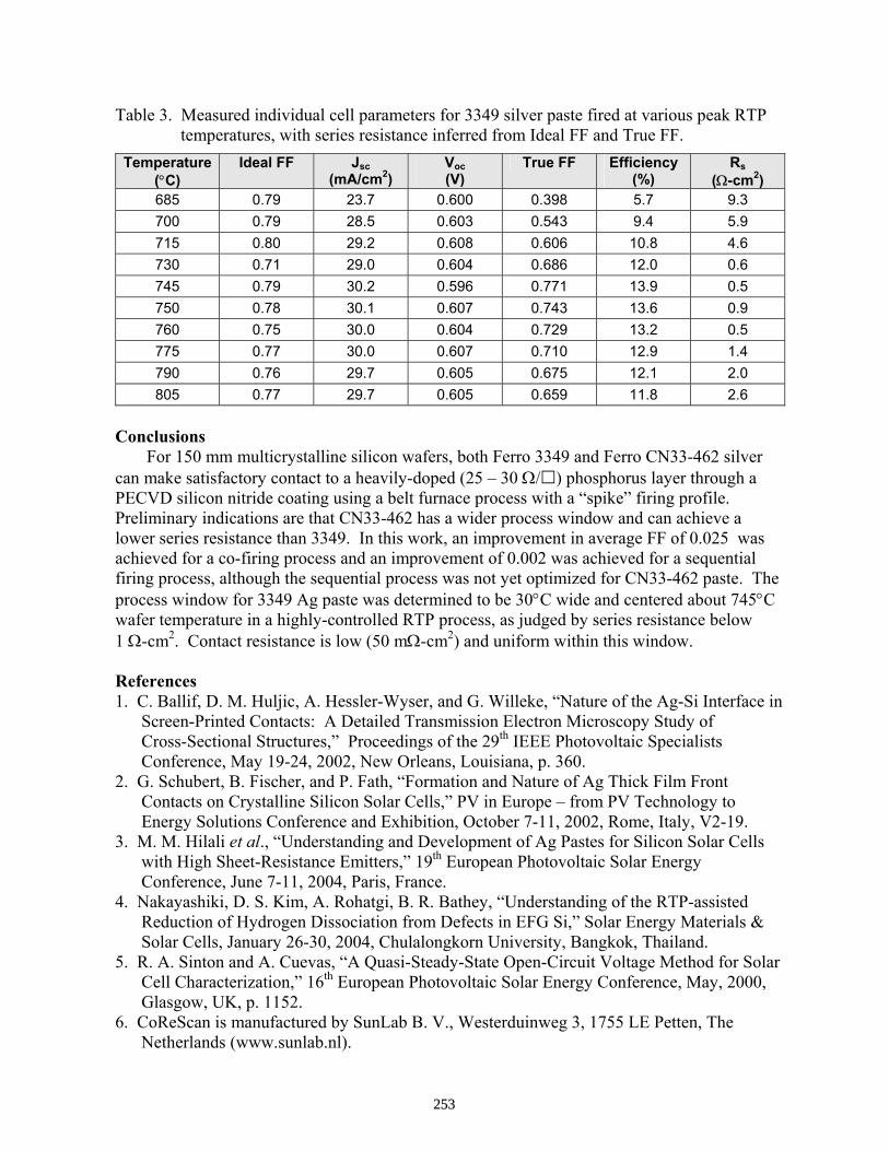
Table 3. Measured individual cell parameters for 3349 silver paste fired at various peak RTP temperatures, with series resistance inferred from Ideal FF and True FF.
Temperature (°C)
Ideal FF Jsc (mA/cm2)
Voc (V)
True FF Efficiency (%)
Rs (Ω-cm2)
685 0.79 23.7 0.600 0.398 5.7 9.3 700 0.79 28.5 0.603 0.543 9.4 5.9 715 0.80 29.2 0.608 0.606 10.8 4.6 730 0.71 29.0 0.604 0.686 12.0 0.6 745 0.79 30.2 0.596 0.771 13.9 0.5 750 0.78 30.1 0.607 0.743 13.6 0.9 760 0.75 30.0 0.604 0.729 13.2 0.5 775 0.77 30.0 0.607 0.710 12.9 1.4 790 0.76 29.7 0.605 0.675 12.1 2.0 805 0.77 29.7 0.605 0.659 11.8 2.6
Conclusions
For 150 mm multicrystalline silicon wafers, both Ferro 3349 and Ferro CN33-462 silver can make satisfactory contact to a heavily-doped (25 – 30 Ω/ ) phosphorus layer through a PECVD silicon nitride coating using a belt furnace process with a “spike” firing profile. Preliminary indications are that CN33-462 has a wider process window and can achieve a lower series resistance than 3349. In this work, an improvement in average FF of 0.025 was achieved for a co-firing process and an improvement of 0.002 was achieved for a sequential firing process, although the sequential process was not yet optimized for CN33-462 paste. The process window for 3349 Ag paste was determined to be 30°C wide and centered about 745°C wafer temperature in a highly-controlled RTP process, as judged by series resistance below 1 Ω-cm2. Contact resistance is low (50 mΩ-cm2) and uniform within this window. References 1. C. Ballif, D. M. Huljic, A. Hessler-Wyser, and G. Willeke, “Nature of the Ag-Si Interface in
Screen-Printed Contacts: A Detailed Transmission Electron Microscopy Study of Cross-Sectional Structures,” Proceedings of the 29th IEEE Photovoltaic Specialists Conference, May 19-24, 2002, New Orleans, Louisiana, p. 360.
2. G. Schubert, B. Fischer, and P. Fath, “Formation and Nature of Ag Thick Film Front Contacts on Crystalline Silicon Solar Cells,” PV in Europe – from PV Technology to Energy Solutions Conference and Exhibition, October 7-11, 2002, Rome, Italy, V2-19.
3. M. M. Hilali et al., “Understanding and Development of Ag Pastes for Silicon Solar Cells with High Sheet-Resistance Emitters,” 19th European Photovoltaic Solar Energy Conference, June 7-11, 2004, Paris, France.
4. Nakayashiki, D. S. Kim, A. Rohatgi, B. R. Bathey, “Understanding of the RTP-assisted Reduction of Hydrogen Dissociation from Defects in EFG Si,” Solar Energy Materials & Solar Cells, January 26-30, 2004, Chulalongkorn University, Bangkok, Thailand.
5. R. A. Sinton and A. Cuevas, “A Quasi-Steady-State Open-Circuit Voltage Method for Solar Cell Characterization,” 16th European Photovoltaic Solar Energy Conference, May, 2000, Glasgow, UK, p. 1152.
6. CoReScan is manufactured by SunLab B. V., Westerduinweg 3, 1755 LE Petten, The Netherlands (www.sunlab.nl).
253

Variation of Screen-Printed Solar Cell Performance Along Commercially Grown Ga- and B-Doped Czochralski Ingots
A. Ebong1, V. Meemongkolkiat1, M. Hilali1, V. Upadhyaya1, B. Rounsaville1, I. Ebong1,
A. Rohatgi1, G. Crabtree2, J. Nickerson2, T. L. Jester2
1 - University Center of Excellence for Photovoltaic Research and Education, School of
Electrical and Computer Engineering, Georgia Institute of Technology, 777 Atlantic Drive, Atlanta, GA 30332-0250
2 - Shell Solar Industries, 4650 Adohr Lane, Camarillo, CA 93011 Abstract A comparison of the variation of resistivity, lifetime, and cell performance, before and after light-induced degradation is made along the B- and Ga-doped Czochralski (Cz) ingots. Significant resistivity variation was found in the Ga-doped Cz ingot, but the efficiency variation was found to be ≤ 0.5%, from 16.4% to 16.9%. No light-induced degradation (LID) was observed in the cells fabricated from the Ga-doped ingot, regardless of the position in the ingot. In contrast, the B-doped ingot showed a very tight resistivity range, resulting in very tight lifetime and efficiency distributions. The cell efficiency was ~16.4% along the entire ingot, but the LID effect reduced the efficiency by about 0.8% absolute. A high-sheet-resistance emitter and surface texturing were successfully implemented to enhance the performance of screen-printed, Ga-doped Cz cells. The combination of a high-sheet-resistance emitter and surface texturing resulted in cell efficiencies as high 17.7% on 1.5 Ω-cm Ga-doped Cz and 18.1% on 1.0 Ω-cm B-doped float zone. 1. Introduction
It is well known that solar cells fabricated on the conventional B-doped Czochralski (Cz) Si suffer from performance degradation caused by illumination or carrier injection. It has also been established that this light-induced degradation (LID) results from the presence of B and O simultaneously in Si. Therefore, the LID effect can be removed by eliminating either one of the two components. Doping a Si ingot with Ga instead of B is a promising way to avoid LID. High efficiency, stable Ga-doped Cz cells have been demonstrated in conjunction with photolithography contacts [1] while moderate efficiencies have been achieved with a manufacturable process using screen-printed contacts. The principal drawback of using Ga as a dopant is the low segregation coefficient of Ga in Si, which results in a wide variation in resistivity along the Ga-doped ingot. The first objective of this paper is to investigate the impact of this resistivity variation and LID on the performance of screen-printed (SP) solar cells.
The second objective of this work is to enhance the efficiency of manufacturable Ga-doped Cz solar cells with SP contacts by implementation of a high-sheet-resistance emitter and surface texturing. Recently, Hilali et al. [2] achieved cell efficiencies in excess of 17% on planar float zone silicon by demonstrating excellent screen-printed contacts on high-sheet-resistance emitters. In this study, we combine a manufacturable process for SP contacts on high-sheet-resistance emitters with surface texturing to achieve Ga-doped Cz cell efficiencies of 17.7% and float zone cell efficiencies of 18.1%.
254

Manufacturable SP solar cells are analyzed using a combination of light and dark I-V, internal quantum efficiency, and bulk lifetime measurements. 2. Experimental
To study the effect of Cz wafer location and resistivity, SP solar cells were fabricated on the wafers taken from six locations along B-doped ingot and nine locations along a Ga-doped ingot. The two ingots were grown at Shell Solar Industries using the same growth method and equipment. The resistivity and lifetime on each location was measured prior to cell processing. All the samples were textured in an alkaline etch and then POCl3 diffused to obtain ~45 Ω/sq emitter. Subsequently, a SiNx AR-coating was deposited on the front surface. All the samples were then subjected to full-area Al screen-printing on the backside followed by Ag gridline printing on the front. The samples were then co-fired in a rapid thermal processing system. The cells were then isolated using a dicing saw to define an active area of 4 cm2 and annealed in forming gas for 18 min.
To investigate LID on Ga-doped and B-doped Cz solar cells, I-V measurements were performed first after annealing the cells at 200°C to remove any effects of LID. The I-V measurements were repeated after light soaking for > 20 hrs to obtain the stabilized cell performance.
High-efficiency Ga-doped Cz and float zone solar cells were fabricated by adjusting the POCl3 diffusion temperature to achieve an n+ emitter sheet resistance of 80-100 Ω/ . For comparison, Ga-doped solar cells with 45 Ω/ emitters were also fabricated. A PECVD SiNx film was then deposited on the front surface of all samples. Next, an Al paste was printed on the rear surface and a specially formulated Ag paste was printed on the front surface in a grid pattern optimized for high-sheet-resistance emitters [2]. Cz and float zone cells were then co-fired in a belt furnace using optimized firing conditions for 80-100 Ω/sq emitters. All cells were then isolated using a dicing saw to define an active area of 4 cm2 and annealed in forming gas for 18 min.
3. Results and Discussion
3.1 Impact of the resistivity variation and LID in Ga- and B-doped Cz on solar cells performance
The resistivity and as-grown lifetime variation from the seed to tail end of the Ga-doped and B-doped Cz ingot is summarized in Table 1. As expected, the resistivity variation is much larger (0.57-2.54 Ω-cm) in the Ga-doped ingot compared to the B-
Ingot Tail end Seed end Location 1 2 3 4 5 6 ρ (Ωcm) 0.87 0.82 0.90 0.95 1.00 1.22 B-doped
As-grown τ (µs) 210 60 200 250 220 160 Location 1 2 3 4 5 6 7 8 9 ρ (Ωcm) 0.57 0.63 0.84 0.99 1.19 1.46 1.82 2.17 2.54 Ga-
doped As-grown τ (µs) 90 120 160 260 330 510 540 760 410
Table 1. Resistivity and as-grown lifetime before LID along the B- and Ga-doped ingots
255

doped ingot. The resistivity decreases appreciably from seed to tail end of the Ga-doped ingot because of the low segregation coefficient of Ga in Si. This also results in wide variation in the bulk lifetime (410-90 µs) from seed to tail end. The variation in solar cell efficiency as a function of ingot location is summarized in Figs. 1 and 2 for B and Ga-doped ingots, respectively. Both the annealed and light-soaked states are included in the figures. The efficiency prior to LID in the B-doped ingot was very uniform (~16.4%) except at the seed end where the efficiency drops slightly to 16.1%. However, the efficiency of all the B-doped cells decreased by about 0.8% absolute after the light-soaking, resulting in final efficiency of ~15.5%. Unlike the B-doped ingot, efficiency spread in Ga-doped ingot prior to the LID is somewhat larger (16.4%-16.9%) with higher resistivity seed-end wafers producing higher efficiency. Nevertheless, this variation in the efficiency is acceptable considering the very wide variation in resistivity. Fig. 3 shows that the spread in Ga-doped cells efficiency is reduced due to the competing effect of increasing Voc and decreasing Jsc as the resistivity decreases. Moreover, there is essentially no degradation observed in the Ga-doped ingot, resulting in ≥ 1% higher absolute efficiency after light soaking relative to the B-doped ingot. However, this gap in efficiency between the B- and the Ga-doped could be reduced if a higher resistivity B-doped ingot is used. Nevertheless, this result shows that Ga doping offers great potential for higher performance Cz cells. In addition, high quality Ga-doped ingot can be grown in the same puller used
Fig. 1. Efficiency of Al-BSF solar cells ondifferent locations of the B-doped ingot Cz.
14.5
15
15.5
16
16.5
17
1 2 3 4 5 6
B-doped ingot location
Eff
icin
ecy
(%)
Annealed stateLight-soaked state
Tail end Seed end
0.87 Ωcm 1.22 Ωcm
Fig. 2. Efficiency of Al-BSF solar cells ondifferent locations of the Ga-doped Cz ingot.
14.5
15
15.5
16
16.5
17
1 2 3 4 5 6 7 8 9
Ga-doped ingot location
Eff
icie
ncy(
%)
Annealed stateLight-soaked state
Tail end Seed end
0.57 Ωcm 2.54 Ωcm
Fig 3. Distribution of Jsc and Voc of solar cellsalong the Ga-doped ingot location.
618
619
620
621
622
623
624
625
626
627
628
1 2 3 4 5 6 7 8
Ga-doped ingot location
Voc
(mV)
33
33.5
34
34.5
35
35.5
36
J sc (
mA/
cm2 )
VocSeries2Series3Jsc
Tail end Seed end0.57 Ωcm 2.54 Ωcm
256
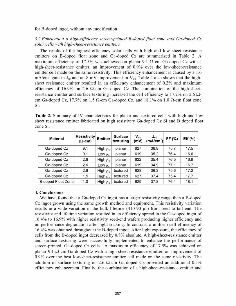
for B-doped ingot, without any modification.
3.2 Fabrication o high-efficiency screen-printed B-doped float zone and Ga-doped Cz solar cells with high-sheet-resistance emitters
The results of the highest efficiency solar cells with high and low sheet resistance emitters on B-doped float zone and Ga-doped Cz are summarized in Table 2. A maximum efficiency of 17.5% was achieved on planar 9.1 Ω-cm Ga-doped Cz with a high-sheet-resistance emitter, an improvement of 0.9% over the low-sheet-resistance emitter cell made on the same resistivity. This efficiency enhancement is caused by a 1.6 mA/cm2 gain in Jsc and an 8 mV improvement in Voc. Table 2 also shows that the high-sheet resistance emitter resulted in an efficiency enhancement of 0.2% and maximum efficiency of 16.9% on 2.6 Ω-cm Ga-doped Cz. The combination of the high-sheet-resistance emitter and surface texturing increased the cell efficiency to 17.2% on 2.6 Ω-cm Ga-doped Cz, 17.7% on 1.5 Ω-cm Ga-doped Cz, and 18.1% on 1.0 Ω-cm float zone Si.
4. Conclusions
We have found that a Ga-doped Cz ingot has a larger resistivity range than a B-doped Cz ingot grown using the same growth method and equipment. This resistivity variation results in a wide variation in the bulk lifetime (410-90 µs) from seed to tail end. The resistivity and lifetime variation resulted in an efficiency spread in the Ga-doped ingot of 16.4% to 16.9% with higher resistivity seed-end wafers producing higher efficiency and no performance degradation after light soaking. In contrast, a uniform cell efficiency of 16.4% was obtained throughout the B-doped ingot. After light exposure, the efficiency of cells from the B-doped ingot decreased by 0.8% absolute. A high-sheet-resistance emitter and surface texturing were successfully implemented to enhance the performance of screen-printed, Ga-doped Cz cells. A maximum efficiency of 17.5% was achieved on planar 9.1 Ω-cm Ga-doped Cz with a high-sheet-resistance emitter, an improvement of 0.9% over the best low-sheet-resistance emitter cell made on the same resistivity. The addition of surface texturing on 2.6 Ω-cm Ga-doped Cz provided an additional 0.5% efficiency enhancement. Finally, the combination of a high-sheet-resistance emitter and
Material Resistivity(Ω-cm) Emitter Surface
texturingVoc
(mV) Jsc
(mA/cm2) FF (%) Eff (%)
Ga-doped Cz 9.1 High ρs planar 627 36.8 75.7 17.5 Ga-doped Cz 9.1 Low ρs planar 619 35.2 76.4 16.6 Ga-doped Cz 2.6 High ρs planar 622 35.4 76.5 16.9 Ga-doped Cz 2.6 Low ρs planar 619 34.9 77.1 16.7 Ga-doped Cz 2.6 High ρs textured 628 36.3 75.6 17.2 Ga-doped Cz 1.5 High ρs textured 627 37.4 75.4 17.7
B-doped Float Zone 1.0 High ρs textured 629 37.8 76.4 18.1
Table 2. Summary of IV characteristics for planar and textured cells with high and lowsheet resistance emitter fabricated on high resistivity Ga-doped Cz Si and B doped floatzone Si.
257

surface texturing resulted in cell efficiencies as high as 17.7% on 1.5 Ω-cm Ga-doped Cz and 18.1% on 1.0 Ω-cm B-doped float zone.
5. References
1. J. Knowbloch, S. Glunz, D. Biro, W. Warta, E. Schaffer and W.Wettling, “Solar Cells
with efficiencies above 21% processed from Czochralski grown silicon” Proc. of the 25th IEEE Photovoltaic Specialists Conf. 1995: 405-408.
2. M. Hilali, A. Rohatgi, S. Asher “Development of screen-printed silicon solar cells
with high fill factors on 100 Ω/sq emitters” IEEE Transactions on Electron Devices, vol. 51 (6), 2004: 948-955.
258
Factors that Limit the Formation of an Uniform and Thick Screen-Printed Al-Back Surface Field
V. Meemongkolkiat, K. Nakayashiki, D. S. Kim, and A. Rohatgi
University Center of Excellence for Photovoltaics Research and Education School of Electrical and Computer Engineering
Georgia Institute of Technology, Atlanta, GA 30332-0250
Abstract Theoretical calculations reveal that the quality of an Al-back surface field (BSF) can be improved by either increasing the thickness of the deposited Al, the peak alloying temperature, or both. However, this study shows that there is a critical temperature for a given printed Al thickness, above which the BSF quality begins to degrade because of non-uniformity. This critical temperature is lower for thicker deposited Al layers and therefore limits the quality or thickness of the Al-BSF that can be achieved before degradation sets in. This non-uniformity of Al-BSF is proposed to be due to agglomeration of the Al-Si melt at higher temperatures. Confirmation of experimental results and theoretical calculations are used to provide guidelines for choosing the optimal combination of Al thickness and alloying temperature. 1. Introduction The screen-printed (SP) Al-back surface field (BSF) is widely used to passivate the back surface of Si solar cells because of its simplicity and cost effectiveness. It is known that a thicker Al-BSF and a higher p+ doping level generally provide a higher quality of passivation. Theoretically, thicker Al-BSF can be obtained by either increasing the thickness of the printed Al or increasing the peak alloying temperature, and the doping level can be increased solely by raising the peak alloying temperature [1]. It is shown in this paper that there exists a critical temperature for a given thickness of printed Al, above which the Al-BSF region becomes highly non-uniform. This places a limit on the thickness and doping concentration that can be achieved before the BSF quality starts to degrade because of non-uniformity. This non-uniformity of an Al-BSF was first investigated by examining the cross-sectional SEM micrographs. The detrimental effect of this non-uniform BSF on solar cell performance is confirmed by fabricating and analyzing solar cells with different combinations of Al printed thickness and peak alloying temperature. The guidelines for choosing the optimum firing temperature for different Al-printed thickness are also presented. 2. Formation and observation of the non-uniform Al-BSF above a critical alloying temperature It was found that when the peak Al-Si alloying temperature is increased above a critical value, many bumps are formed on the external Al surface after firing that are visible to the naked eye (Fig. 1). The size of these bumps becomes larger when thicker Al is applied. To examine the effect of these bumps on the uniformity and quality of the Al-BSF, the cross-sectional SEM micrographs were taken at and around the regions where the bumps were observed (Fig. 2). The Al-BSF region was delineated from the Si bulk by etching the sample in 1:3:6-HF:HNO3:CH3COOH for 10 s [2]. It can be seen clearly in
259

Fig. 2 that the Al-BSF is very thick at the peak of the bump; however, the Al-BSF around the bump or slightly away from it is very thin. Based on the examination of the cross-sectional morphology and the Al-BSF melt and re-growth process [3], it is proposed that this non-uniform BSF occurs as a result of agglomeration of the Al-Si melt when the melt is at high temperature. This results in a large amount of melt at the agglomerated regions, leaving behind less melt around them. When the sample cools down, the re-growth of Al-BSF region is very non-uniform, with very thick BSF region near the peak of the bumps and very thin BSF regions around the bump.
a) b) c)
Fig. 1. Formation of bumps on the post-fired Al surface after 925°C heat treatment on samples with Al thickness of a) 24µm, b) 40 µm, and c) 62 µm.
Fig. 2. Cross-sectional SEM micrograph of a bump (agglomerated) region in a Si sample
with 24 µm of Al annealed at 925°C n RTP. 3. Determination of the critical temperature for a given Al thickness at which the agglomeration occurs
Attempts were made to identify the critical temperature where the agglomeration begins to occur. Three different thicknesses of Al were printed on the Si samples: 24 µm, 40 µm, and 62 µm (thicknesses were measured by SEM after firing). The alloying was performed in a rapid thermal processing (RTP) system with a ramp-up rate of 50°C/s and a dwell time of 5 s. The peak temperature was varied from 700°C to 925°C in 25°C increments. The onset of agglomeration was defined when the Al-BSF region became 20% greater than the average Al-BSF thickness. It should be noted also that even though
SiAl-BSF
Si-Al alloy
Cavities and Al-Si eutectic
Very thick BSF
Very thin BSF
260

agglomeration occurs, it is not visible unless the temperature is much greater than the critical or onset temperature for agglomeration. The critical temperature for 24 µm, 40 µm, and 62 µm thick Al were determined by cross-sectional SEM analysis based on the 20% criterion. These data points were used to plot the curve, shown in Fig. 3, for the highest temperature that can be reached without agglomeration as a function of the Al thickness. This is what limits the thickness of a uniform Al-BSF that can be achieved because we cannot take full advantage of increasing the alloying temperature to increase the Al-BSF thickness.
740760780800820840860880900
10 20 30 40 50 60 70Al thickness (µm)
Peak
tem
pera
ture
(°C
)
Al-Si melt agglomeration
Fig. 3. Highest alloying peak temperature and corresponding Al thickness (measured
after firing) where the agglomeration of Al-Si melt can be avoided.
4. Effect of the agglomeration of the Al-Si melt on the BSF quality and solar cell performance To examine the effect of a non-uniform BSF caused by agglomeration, SP Al-BSF solar cells were fabricated with several combinations of temperature and Al thickness on 1.3 Ω-cm, p-type float zone Si. First, the n+-emitter region for all the cells was formed by diffusion in a POCl3 furnace to obtain a ~45 Ω/sq emitter. Following phosphorus glass removal, a PECVD SiNx AR-coating was deposited on the front surface of all samples. Samples were then subjected to full-area Al screen-printing on the backside using three different screens to print three different Al thicknesses. Subsequently, the samples were fired in an RTP system with different combinations of Al-thickness and temperature (total of seven samples). The Ag gridlines were screen-printed on the front, followed by RTP front contact firing at 700°C. Figure 4 shows that for the 24 µm thick Al, for which the critical temperature was 875°C (Fig. 3), an increase in firing temperature from 750°C to 875°C increased the Voc from 618 to 624 mV because of the increase in Al-BSF thickness and the absence of agglomerations. However, in the case of the 60 µm thick Al (critical temperature=750°C), an increase in firing temperature from 750°C to 875°C reduced the Voc from 634 mV to 623 mV. This is the result of the formation of agglomerations at 875°C. Theoretical calculations revealed that, in the absence of agglomeration, a 60 µm thick Al layer fired at 875°C should have produced an Al-BSF with a thickness of 29 µm, resulting in a Voc of 642 mV. This shows how the Al-Si melt agglomeration puts a limit on achieving a uniformly thick Al-BSF and higher Voc.
261

20
30
4050
60
700
750
800
850
900615
620
625
630
635
624
625 623
618
632
631
634
Fig. 4. Voc of solar cells with different combinations of peak alloying temperature and Al thickness.
5. Conclusions It was found that there is a critical alloying temperature for a given Al-thickness above which the Al-BSF becomes non-uniform and cell performance starts to degrade. This critical temperature is lower for thicker Al layers, which puts a limit on the maximum thickness as well as the highest doping concentration that can be achieved in the Al-BSF region. This paper shows that the non-uniform Al-BSF is the result of agglomeration of the Al-Si melt at higher temperatures and is responsible for a huge variation in the Al-BSF thickness. It was demonstrated that this non-uniformity in the BSF has a detrimental effect on solar cell performance, which can reduce Voc by as much as 11 mV. Finally, we have provided the guidelines for choosing the Al-thickness and peak firing temperature to avoid the formation of Al-Si melt agglomeration and achieve the maximum Voc. REFERENCES [1] S. Narasimha, A. Rohatgi, and A.W. Weeber, “An Optimized Rapid Aluminum
Back Surface Field Technique for Silicon Solar Cells”, IEEE Transactions on Electron Devices 46, 1363 (1999).
[2] W.R. Runyan, Semiconductor Measurements and Instrumentation, (McGraw-Hill, New York, 1975).
[3] J.D. Alamo, J. Eguren, and A. Luque, “Operating Limits of Al-Alloyed High-Low Junctions for BSF Solar Cells”, Solid-State Electron 24, 415 (1981).
Agglomeration
262

COMPARISON OF BATCH AND INLINE WET PROCESSING SYSTEMS
J. Osterkamp, G. Knoch ASTEC GmbH
Am Roethenbuehl 7, 92348 Berg, Germany Tel +49 (9189) 44040, Fax +49 (9189) 440450, [email protected]
ABSTRACT: It is expected that till the end of 2010 Mono- and Polycrystalline Silicon cells together with Ribbon Silicon cells will still have a common market share of 75% and continue to be the backbone of photovoltaic systems. [1] It is the common target by 2010 to achieve costs of less than 1 EUR/Wp for c-Si PV systems. Therefore further developments in cutting and handling of thinner wafers (~ 80 µm thickness) will have to be made and new surface processes for cell manufacturing are being developed and will be optimized. This outlook as well as the fact that some cell processes are necessarily single wafer inline processes led to the idea of using also inline wet processing equipment for cleaning and etching of crystalline silicon cells. Together with the development of new wet processes (i.e. acidic Iso-Texturing) it became possible to demonstrate successfully the wafer treatment in wet inline equipment for mass production which was dominated for more than 25 years by wet batch processing. This contribution compares batch versus inline wet process equipment. The reader will get both an overview of the advantages and risks of both types, and support for choosing the right equipment for his own requirements. 1 INTRODUCTION Since the first development of solar cells all crystalline silicon wafers were always immersed into liquid chemicals and water to achieve designated surface conditions. The treatment of the wafers occurred always manually step by step as a single wafer process immersing one wafer in different baths or as a batch process immersing a batch of typically 25 wafers into different vessels. It has always been the target of the PV industry to make solar power competitive to fossil or nuclear power. One way to reduce costs has been the mass production of solar cells. Now batches of 200 to 250 wafers are immersed in tanks and automatically transferred by robot systems through the different process steps in a wet bench. Indeed modifications and improvements have been made but during the last 25 years no fundamental equipment design changes have taken place. Of course, due to moving from mono crystalline towards poly crystalline material as well as further process development, increasing environmental aspects and new technical possibilities, the equipment design has changed slightly, not the general function of batch processing though. With the development of inline diffusion, sinter and deposition equipment it is welcomed to have also inline wet processing equipment available. It was predicted to increase the yield, to reduce the wafer breakage rate and to reduce the costs. In the meantime the Texturisation of solar cells became already state of the art to increase the cell efficiency. Unfortunately the process time for alkaline Anisotropic Texturisation of mono crystalline silicon cells is rather long (> 20 min) necessitating very long inline equipment and by that resulting higher costs.
263

Not until after the development of an Isotropic Texturisation process with much shorter process times it became very interesting to have inline wet processing tools. In the meantime it became possible to demonstrate successfully the wafer treatment in wet inline equipment for mass production which was dominated for more than 25 years by wet batch processing. Advantages and risks of both types of equipment will be discussed below and support for choosing the right equipment will be given.
Figure 1: Automatic, completely closed wet bench for mass production of solar cells (1978) Figure 2: Automatic,
completely closed wet bench for mass production of solar cells (2002) Figure 3: Automatic, completely
closed inline wet bench for mass production of solar cells (2003)
2 ADVANTAGES AND RISKS 2.1 Wafer handling This point is a clear benefit of an inline system. A quick transfer time from a process bath into a rinse bath to stop the etching process in a short and always reproducible time is very easily achieved with the continuous treatment. It also avoids the risk of wafer breakage caused by quick carrier transfers. The integration of an inline system into a continuous product flow is much easier than that of a batch system. Wafer processing is not interrupted by wafer handling which leads to a further reduction of wafer breakage. Finally an inline system does not bear the risk of wafer sticking. This risk may occur in batch systems where wafers are vertically placed in a carrier. When lifted out of the liquid wafers are bend by the surface tension (meniscus) of the liquid between those wafers and, if their distance is not big enough, they may stick together. This can then results in a non uniform surface treatment, spots on the wafer surface and wet wafers. 2.2 Cost of ownership Investment costs and running costs are to be considered when we do a cost of ownership calculation. If the equivalent inline and batch systems are compared it can be seen that the investment costs for these machines are almost the same. Additional investment into suitable wet process wafer cassettes has to be taken into account for a batch system.
264

On the other hand it is must be noted that an inline system needs automatic three dimensional buffer systems integrated in the production line. The third dimension of the buffer is necessary if it is required to buffer for example half an hour of production capacity. If we assume a throughput of 1,200 w/h in 5 tracks and a wafer dimension of 125 x 125 mm² then it would be necessary to have 2-dimensional buffers of 1,200 w/h / 5 x ½ h x 125 mm = 15 m length after each production tool in the line. If in an inline etching machine are additional exhaust hoods are directly above the etch baths it is easier to collect the waste gas and less exhaust volume is necessary than with a batch system. This lower exhaust volume results in a cheaper exhaust scrubber. The comparison of the necessary chemical tank volumes works out equally. While in batch process equipment the tank volume depends on the maximum wafer dimension designed in, the tank volume in inline equipment depends on the necessary processing time in one bath and herewith with the length of the bath. Finally, the carry over from a process bath into a rinse bath is bigger in an inline system than in a batch system. Indeed there is no additional carrier surface on which chemicals can be carried over. It is obvious, however, that on a horizontal wafer surface more chemicals are carried over than on a vertical wafer surface. This ends in a higher chemical consumption in an inline system compared to a batch system. The costs for equipment space are nearly equal because the footprint of both equipments is very similar. This is valid as long as acidic Texturisation equipment is compared. Due to the long process time of alkaline Texturisation processes it would be necessary to build very long inline equipment compared to batch systems. 2.3 Process The simultaneous treatment of several single wafers in an inline system guarantees an equal surface conditioning for all wafers. To achieve the same results in a batch process much more efforts and mechanically design conditions are necessary. With special open carriers and a sophisticated flow distribution in the process baths it is without doubt possible to achieve very satisfying results in a batch system. In processes with gas development special measures are necessary in an inline system for removal of gas bubbles created at the lower side. 2.4 Logistics As already mentioned before the integration of an inline system in a continuous process flow is easier than of a batch system. Additionally, the wafer transfer control is very simple compared to the complex robot control system of a batch system. The situation changes if we consider cases where in an inline production integration buffer systems become necessary. This happens for example during the necessary bath changes in a wet processing tool or any stop in the complete production line. In these cases it is necessary to control the logistics of buffering. Even with the best process some wafers may not pass final inspection but can be recovered by exposing them to certain process steps again. In a batch system this can be done by simply selecting the desired and necessary single process steps. This way these wafers are reworked according to selected procedures. Such specific rework of wafers has serious limitations with an inline system. Finally more and more module manufacturers request from their cell manufacturers information about the process parameters of the delivered cells. Such a lot tracking can easily be made in a batch system by the carriers used which have to be equipped with transponders. All necessary information
265

can be stored for quality control and long-term backtracking of product data. With an inline system it would be necessary to track either wafers marked individually or track the wafer processing with time. 2.5 Flexibility If we look at the dynamics of the PV industry and the herewith related progresses in wet processing and changes in wafer dimensions during the past few years, it is obvious that a high flexibility of the processing equipment is necessary to spread the investment over a long equipment utilization time. The necessity of high equipment flexibility will continue into the future (thinner wafers, larger wafer dimensions, new wet processes). New planned equipment will normally already be designed for a wafer dimension up to 210 mm x 210 mm. In the case of an inline system the number of processed wafers depends on the wafer dimension. The maximum achievable MWp throughput performance is nearly independent from the wafer dimension. The maximum throughput calculated on MWp depends on the transport speed multiplied by the total width of all wafers processed in parallel. That means if an inline equipment has 8 wafer tracks for 100 x 100 mm² wafers (=> 8 x 100 = 800 mm = 100% throughput) it can be changed into 6 wafer lines for 125 x 125 mm² wafers (=> 6 x 125 = 750 mm = 94% throughput) 5 wafer lines for 156 x 156 mm² wafers (=> 5 x 156 mm = 785 mm = 98% throughput ) or 4 wafer tracks for 210 x 210 mm² (=> 4 x 210 = 840 mm = 105% throughput). In a batch system the maximum achievable MWp throughput performance depends on the number of wafers processed in one tank at a time and the wafer size. When Texturisation of wafers became nearly state of the art, cell manufacturers considered the possibility of switching between processes, anisotropic etching and isotropic etching, or to enlarge their product portfolio to mono- and polycrystalline cells. These approaches can only be realized, however, with the flexibility of a batch system. Decision makers should bear in mind that in an inline system all process times have an extreme dependence on the gating process time. As long as the bath length of each bath and herewith its process time is designed to the specific needs the inline system is unbeatable. But as soon as one or two single process times shall be changed it is nearly impossible to do that without influence on the process parameters and process times in other baths. This is a unique strength of a batch system. Finally we like to point out again that it is only possible with a batch system to rework wafers if they do not fulfill the requirements. 3 SUMMARY Inline systems lend themselves to integration in the process flow as long as the necessary buffers are also integrated in the production line. Batch systems feature high flexibility for further process adaptations and optimization as well as the possibility of wafer rework. Depending on which feature is more important for a decision maker he will find both optimized batch and innovative inline processing systems on the market. Both types will justify their existence for quite some time. The sister companies RENA and ASTEC are committed to have both types available incorporating the latest innovative developments.
266

4 REFERENCES [1] Bank Sarasin, Christoph Butz, Sarasin Research PV 2002, August 2002 (19)
267

Near Infrared Photoelasticity of Polycrystalline Silicon and it’s Relation to Solar Cell Processing
S. He, S. Danyluk, A. Rohatgi, A. Upadhyaya, V. Yelundur
Georgia Institute of Technology
I. Tarasov, S. Ostapenko University of South Florida
Abstract
This paper summarizes the research on the monitoring of the evolution of residual stresses and lifetime of commonly used photovoltaic samples. The residual stress and lifetime are characterized using a full-field polariscope and room temperature photoluminescence (PL) & surface photovoltage (SPV) respectively. The correlation between the residual stresses and minority lifetime is presented.
1 Introduction
There are a number of ways to produce sheet silicon as a substrate for photovoltaic cells. Methods include the growth of boules, and castings that are cut into sheet, and direct growth of sheet by the edge-defined film growth (EFG) or string processes. These starting materials are believed to contain residual stresses because of the thermal gradients in the solidification process, and cutting and cell processing further cause the redistribution of the residual stresses. When the sheet is cut out of bulk material, warpage can occur as a result of out-of-plane residual stresses, however flat sheet can also contain in-plane residual stresses which can contribute to fracture and degraded mechanical properties. The perimeter of the sheet, and in some cases the front and back surfaces, may contain micro-cracks, which will eventually propagate and fracture the cell if they fall in the regions of tensile residual stresses.
Besides fracture, residual stresses can also generate and propagate dislocations and it is believed that this will eventually impact election-hole lifetimes and thus the efficiencies of photovoltaic cells. As sheet becomes thinner, the grown-in residual stresses, coupled with the stresses imposed during manufacturing, is a more significant problem. There has been a significant effort [1] in the past to develop non-contact techniques to expose the in-plane residual stresses, but none of this work is of sufficient robustness or sensitivity to implement in the manufacturing of photovoltaic cells. Our work is focused on developing a robust, non-contact (optical) method to determine the stress distribution in the sheet silicon, validate the technique in a statistically significant set of experiments and apply the techniques to photovoltaic sheets at various stages of cell processing so that the evolution of the stress distribution can be understood and perhaps optimized.
268

2 Experimental Methods 2.1 Residual stress The residual stresses were measured by a full-field near infrared (NIR) circular polariscope [2]. Figure 1 shows the schematic diagram of the experimental setup. It consists of a halogen lamp as the light source, two polarizers, two waveplates, two spherical lenses (not shown), a digital camera and a narrow band pass infrared filter (not shown). The sample is fixed on a stage placed between the two polarizers. The infrared filter has a wavelength close to the transparent edge of silicon, 1.15 µm, and a bandwidth of 10 nm. The background light is carefully blocked to minimize the contamination of the images. The residual stresses inside the samples change the polarization state of the transmitted light by virtue of photoelastic effect. This change is transferred into an intensity variation in the infrared images of the polariscope. Phase stepping [3] is used to extract the photoelastic parameters, which is further converted to residual stresses using the anisotropic optic-stress law[4]. One measurement takes approximately 30 seconds, including image capturing and data processing. The sensitivity is 1.5 MPa [5], and the current spatial resolution is ~1 mm.
Light source
Polarizer
Waveplate
Sample
Waveplate ( )
Analyzer ( )
Camera
Figure 1: The experimental setup of the infrared residual stress polariscope
2.2 Photoluminescence and Lifetime Measurements
The lifetime was measured by room temperature photoluminescence (PL) [6]. The excitation source of the PL is an Ar laser with a wavelength of 514 nm and power up to 300 nW, which is modulated by a mechanical chopper. Alternatively, an 800 nm AlGaAS laser diode with 10 nm bandwidth operating in a pulse mode with a peak power up to 140 mW was also used. The spot size of both lasers was approximately 0.5 mm. The PL spectra are analyzed using a Spex-500M grating spectrometer and the intensity is captured by a liquid-nitrogen cooled Ge detector. The PL signal was corrected for the spectral response of the optical setup and further processed using a conventional lock-in technique. Full field mapping is accomplished by using an x-y translation stage. Spatial resolution was controlled by the diameter of the laser spot, which ranges from 60 µm to 1 mm. The band-to-band PL intensity h = 1.09eV at room temperature is proportional to the effective lifetime of minority carriers [6] in crystalline silicon, therefore, this measurement can serve as an independent parameter to track the evolution of the electronic qualities in cell processing. The bulk lifetime was measured by the surface photovoltage (SPV) technique, which is critically dependent on the surface condition, or the surface recombination velocity, and thus not all samples show a detectable SPV signal. 2.3 In-Plane Residual Stresses, Measurements of Wafers at Various Stages of Processing
The techniques discussed above were used to monitor the evolution of residual stresses and lifetime during processing. As shown in Figure 2, solar cells were characterized after each manufacturing step by the polariscope, the PL and the SPV. Three single crystal CZ wafers, ten cast blanks, nine EFG and ten Ribbon samples were provided by PV system manufacturers for the test. The major processing steps involve cleaning & etching, diffusion, anti-refection coating and front/back surface contact. After each step, the
269

residual stress and PL were measured except when the samples were covered with front and back contact, while the PL still can be measured at the areas not covered by the contact fingers. The efficiency mapping was carried out after the cell was formed. After that, the back and front contacts were removed, and the substrates etched to obtain the dislocation density maps. All the techniques except the dislocation mapping are non-destructive in nature.
Bare wafers
Cleaning & etching
Diffusion
Anti-reflection coating
Front/back contact
Back surface contactremoval
Final report
Residual stressPL mappingSPV
PL mappingEfficiency
Residual stressPL mappingDislocation mapping
Solar cell processing
Figure 2: Flowchart of solar cell processing 3. Experimental Results 3.1 Residual stresses
The orientation of the residual stresses is critical to the propagation of micro cracks because it determines the crack propagation mode. The fracture toughness, Kc , is lower for mode I, or opening mode crack [7], which is caused by tension loading to move the two crack faces apart. Figure 3(a) shows the typical probability distribution of the orientation for an EFG sample, which is similar to that of the ribbon samples. Cast and CZ samples do not show a consistent pattern. It can bee seen that the orientation of the residual stress in most areas is closely aligned along the horizontal or vertical
direction, which is correlated to the crystal growth direction. In those areas, the average residual stress also has a higher magnitude. This correlation can also be observed from the probability distribution of the residual stress shown in Figure 3(b). The shape of the distribution is close to 2χ distribution. As the magnitude of residual stresses increases, the average orientation is closer to 2/π . This means that the stress with a high magnitude is more likely aligned along the crystal growth direction. Therefore, it is critical to determine the residual stress in order to control the breakage.
(a)
(b)
Figure 3: Probability distribution of the (a) magnitude and (b) orientation of the residual stress in
EFG ribbon wafer
270

The change in average residual stress in processing is shown in Table 1. These data show that there is a significant decrease in the average residual stress for the cast and CZ samples after etching & cleaning, while an increase is observed in the EFG and ribbon wafers. It is hypothesized that the etching & cleaning processing removed the surface layer, which is the main contributor to the residual stress because it was heavily damaged by sawing. The maximum residual stress in EFG and Ribbon samples are supposed to be higher than measured because the spatial dimension of the localized residual stresses is smaller than the spatial resolution of the polariscope. Table 1: Average residual stress in processing (MPa)
Bare Etched Diffused AR coated
CZ 5.92 1.93 1.87 3.41 Cast 3.59 1.76 2.02 5.80 EFG 3.94 6.48 5.91 4.78
Ribbon 4.44 7.31 5.15 5.00
3.2 Photoluminescence
The change in average PL in processing is shown in Table 2. A slight decrease in the PL is observed after the cleaning and etching step. This decrease in PL is mainly caused by the increase of the surface recombination velocity when the silicon dioxide, a surface passivation layer, is stripped. On the other hand, more than a 10-fold increase in PL intensity is observed in all samples except CZ-Si after P-diffusion. This increase is attributed to the upgrade of bulk lifetime due to the phosphorous gettering mechanism. However, the lifetime of CZ-Si wafers can not be upgraded because the single crystal has much better quality and there are not many defects available for gettering. A doubling in the lifetime is achieved when the surface is passivated by the anti-reflection coating, SiN, on the front surface.
Table 2: Average PL in processing (arbitrary unit)
Bare Etched Diffused AR-coated CZ 11.96 6.62 5.27 21.24 Cast 7.12 5.00 46.79 99.61 EFG 5.12 2.14 20.55 50.22 Ribbon 3.30 1.76 33.65 86.26
It is interesting that a circular pattern is observed in PL images in Figure 4 of CZ-Si wafers. This may indicate the appearance of the “ring” defects and/or non-uniformity along the radial direction.
Figure 4: Ring pattern in CZ wafer after diffusion
271
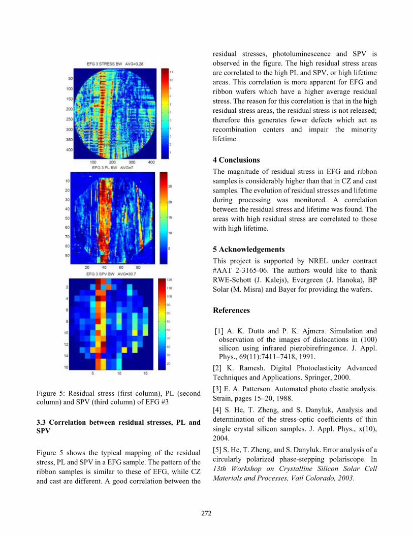
Figure 5: Residual stress (first column), PL (second column) and SPV (third column) of EFG #3 3.3 Correlation between residual stresses, PL and SPV Figure 5 shows the typical mapping of the residual stress, PL and SPV in a EFG sample. The pattern of the ribbon samples is similar to these of EFG, while CZ and cast are different. A good correlation between the
residual stresses, photoluminescence and SPV is observed in the figure. The high residual stress areas are correlated to the high PL and SPV, or high lifetime areas. This correlation is more apparent for EFG and ribbon wafers which have a higher average residual stress. The reason for this correlation is that in the high residual stress areas, the residual stress is not released; therefore this generates fewer defects which act as recombination centers and impair the minority lifetime.
4 Conclusions The magnitude of residual stress in EFG and ribbon samples is considerably higher than that in CZ and cast samples. The evolution of residual stresses and lifetime during processing was monitored. A correlation between the residual stress and lifetime was found. The areas with high residual stress are correlated to those with high lifetime.
5 Acknowledgements This project is supported by NREL under contract #AAT 2-3165-06. The authors would like to thank RWE-Schott (J. Kalejs), Evergreen (J. Hanoka), BP Solar (M. Misra) and Bayer for providing the wafers.
References [1] A. K. Dutta and P. K. Ajmera. Simulation and
observation of the images of dislocations in (100) silicon using infrared piezobirefringence. J. Appl. Phys., 69(11):7411–7418, 1991.
[2] K. Ramesh. Digital Photoelasticity Advanced Techniques and Applications. Springer, 2000. [3] E. A. Patterson. Automated photo elastic analysis. Strain, pages 15–20, 1988. [4] S. He, T. Zheng, and S. Danyluk, Analysis and determination of the stress-optic coefficients of thin single crystal silicon samples. J. Appl. Phys., x(10), 2004. [5] S. He, T. Zheng, and S. Danyluk. Error analysis of a circularly polarized phase-stepping polariscope. In 13th Workshop on Crystalline Silicon Solar Cell Materials and Processes, Vail Colorado, 2003.
272
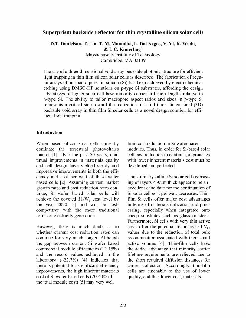
Superprism backside reflector for thin crystalline silicon solar cells
D.T. Danielson, T. Lin, T. M. Montalbo, L. Dal Negro, Y. Yi, K. Wada, & L.C. Kimerling*
Massachusetts Institute of Technology Cambridge, MA 02139
The use of a three-dimensional void array backside photonic structure for efficient light trapping in thin film silicon solar cells is described. The fabrication of regu-lar arrays of air macro-pores in silicon (Si) has been achieved by electrochemical etching using DMSO-HF solutions on p-type Si substrates, affording the design advantages of higher solar cell base minority carrier diffusion lengths relative to n-type Si. The ability to tailor macropore aspect ratios and sizes in p-type Si represents a critical step toward the realization of a full three dimensional (3D) backside void array in thin film Si solar cells as a novel design solution for effi-cient light trapping.
Introduction Wafer based silicon solar cells currently dominate the terrestrial photovoltaics market [1]. Over the past 50 years, con-tinual improvements in materials quality and cell design have yielded steady and impressive improvements in both the effi-ciency and cost per watt of these wafer based cells [2]. Assuming current market growth rates and cost-reduction rates con-tinue, Si wafer based solar cells will achieve the coveted $1/Wp cost level by the year 2020 [3] and will be cost-competitive with the more traditional forms of electricity generation. However, there is much doubt as to whether current cost reduction rates can continue for very much longer. Although the gap between current Si wafer based commercial module efficiencies (12-15%) and the record values achieved in the laboratory (~22.7%) [4] indicates that there is potential for significant efficiency improvements, the high inherent materials cost of Si wafer based cells (20-40% of the total module cost) [5] may very well
limit cost reduction in Si wafer based modules. Thus, in order for Si-based solar cell cost reduction to continue, approaches with lower inherent materials cost must be developed and perfected. Thin-film crystalline Si solar cells consist-ing of layers <30um thick appear to be an excellent candidate for the continuation of Si solar cell cost per watt decreases. Thin-film Si cells offer major cost advantages in terms of materials utilization and proc-essing, especially when integrated onto cheap substrates such as glass or steel.. Furthermore, Si cells with very thin active areas offer the potential for increased Voc values due to the reduction of total bulk recombination associated with their small active volume [6]. Thin-film cells have the added advantage that minority carrier lifetime requirements are relieved due to the short required diffusion distances for carrier collection. Accordingly, thin-film cells are amenable to the use of lower quality, and thus lower cost, materials.
273
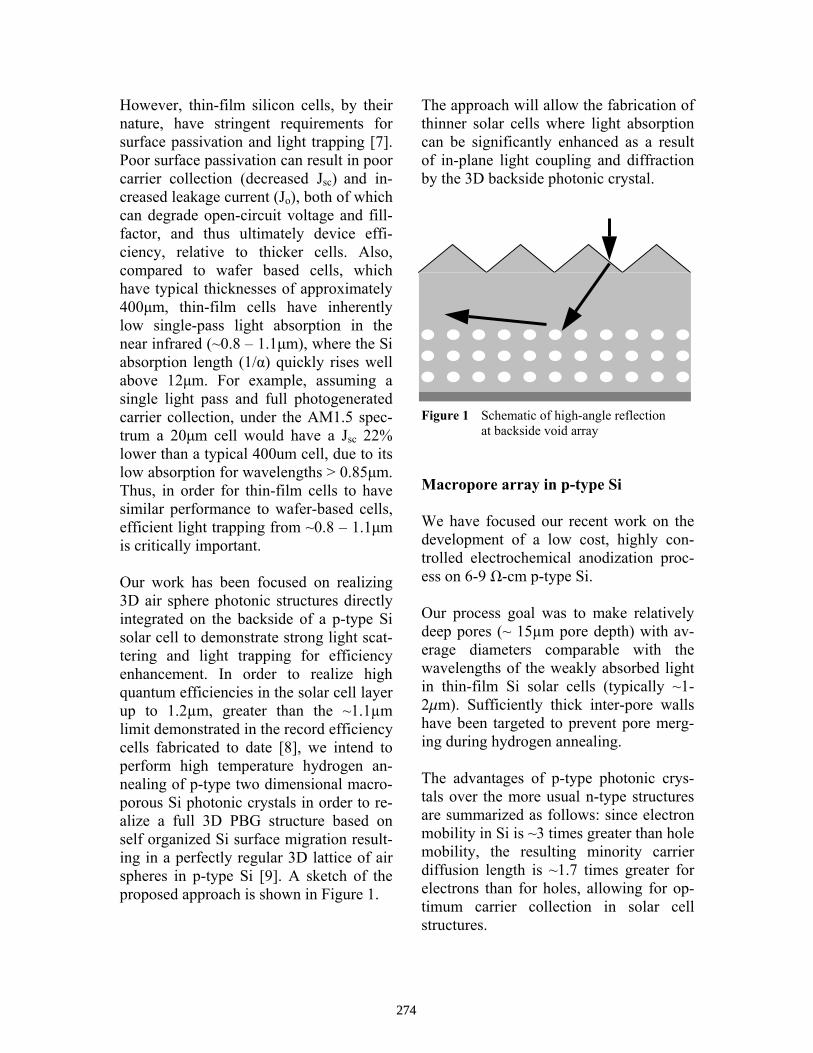
However, thin-film silicon cells, by their nature, have stringent requirements for surface passivation and light trapping [7]. Poor surface passivation can result in poor carrier collection (decreased Jsc) and in-creased leakage current (Jo), both of which can degrade open-circuit voltage and fill-factor, and thus ultimately device effi-ciency, relative to thicker cells. Also, compared to wafer based cells, which have typical thicknesses of approximately 400µm, thin-film cells have inherently low single-pass light absorption in the near infrared (~0.8 – 1.1µm), where the Si absorption length (1/α) quickly rises well above 12µm. For example, assuming a single light pass and full photogenerated carrier collection, under the AM1.5 spec-trum a 20µm cell would have a Jsc 22% lower than a typical 400um cell, due to its low absorption for wavelengths > 0.85µm. Thus, in order for thin-film cells to have similar performance to wafer-based cells, efficient light trapping from ~0.8 – 1.1µm is critically important. Our work has been focused on realizing 3D air sphere photonic structures directly integrated on the backside of a p-type Si solar cell to demonstrate strong light scat-tering and light trapping for efficiency enhancement. In order to realize high quantum efficiencies in the solar cell layer up to 1.2µm, greater than the ~1.1µm limit demonstrated in the record efficiency cells fabricated to date [8], we intend to perform high temperature hydrogen an-nealing of p-type two dimensional macro-porous Si photonic crystals in order to re-alize a full 3D PBG structure based on self organized Si surface migration result-ing in a perfectly regular 3D lattice of air spheres in p-type Si [9]. A sketch of the proposed approach is shown in Figure 1.
The approach will allow the fabrication of thinner solar cells where light absorption can be significantly enhanced as a result of in-plane light coupling and diffraction by the 3D backside photonic crystal. Figure 1 Schematic of high-angle reflection at backside void array Macropore array in p-type Si We have focused our recent work on the development of a low cost, highly con-trolled electrochemical anodization proc-ess on 6-9 W-cm p-type Si. Our process goal was to make relatively deep pores (~ 15µm pore depth) with av-erage diameters comparable with the wavelengths of the weakly absorbed light in thin-film Si solar cells (typically ~1-2mm). Sufficiently thick inter-pore walls have been targeted to prevent pore merg-ing during hydrogen annealing. The advantages of p-type photonic crys-tals over the more usual n-type structures are summarized as follows: since electron mobility in Si is ~3 times greater than hole mobility, the resulting minority carrier diffusion length is ~1.7 times greater for electrons than for holes, allowing for op-timum carrier collection in solar cell structures.
274
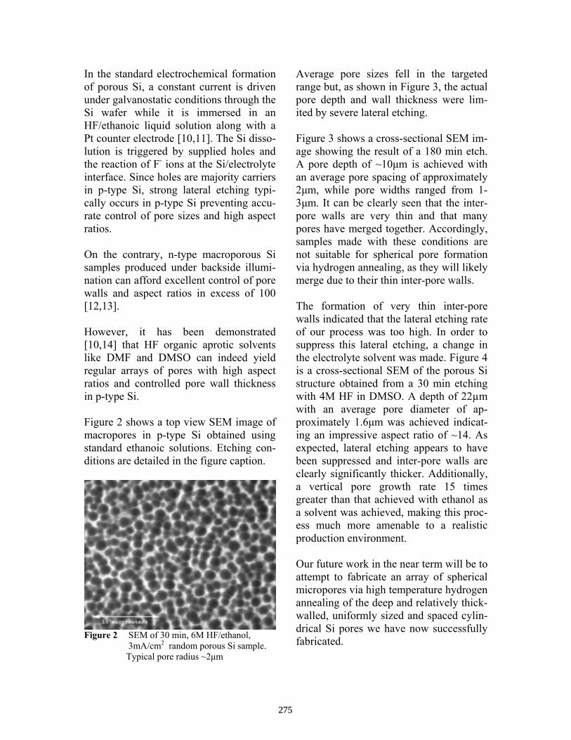
In the standard electrochemical formation of porous Si, a constant current is driven under galvanostatic conditions through the Si wafer while it is immersed in an HF/ethanoic liquid solution along with a Pt counter electrode [10,11]. The Si disso-lution is triggered by supplied holes and the reaction of F- ions at the Si/electrolyte interface. Since holes are majority carriers in p-type Si, strong lateral etching typi-cally occurs in p-type Si preventing accu-rate control of pore sizes and high aspect ratios. On the contrary, n-type macroporous Si samples produced under backside illumi-nation can afford excellent control of pore walls and aspect ratios in excess of 100 [12,13]. However, it has been demonstrated [10,14] that HF organic aprotic solvents like DMF and DMSO can indeed yield regular arrays of pores with high aspect ratios and controlled pore wall thickness in p-type Si. Figure 2 shows a top view SEM image of macropores in p-type Si obtained using standard ethanoic solutions. Etching con-ditions are detailed in the figure caption.
Figure 2 SEM of 30 min, 6M HF/ethanol,
3mA/cm2 random porous Si sample. Typical pore radius ~2µm
Average pore sizes fell in the targeted range but, as shown in Figure 3, the actual pore depth and wall thickness were lim-ited by severe lateral etching. Figure 3 shows a cross-sectional SEM im-age showing the result of a 180 min etch. A pore depth of ~10µm is achieved with an average pore spacing of approximately 2µm, while pore widths ranged from 1-3µm. It can be clearly seen that the inter-pore walls are very thin and that many pores have merged together. Accordingly, samples made with these conditions are not suitable for spherical pore formation via hydrogen annealing, as they will likely merge due to their thin inter-pore walls. The formation of very thin inter-pore walls indicated that the lateral etching rate of our process was too high. In order to suppress this lateral etching, a change in the electrolyte solvent was made. Figure 4 is a cross-sectional SEM of the porous Si structure obtained from a 30 min etching with 4M HF in DMSO. A depth of 22µm with an average pore diameter of ap-proximately 1.6µm was achieved indicat-ing an impressive aspect ratio of ~14. As expected, lateral etching appears to have been suppressed and inter-pore walls are clearly significantly thicker. Additionally, a vertical pore growth rate 15 times greater than that achieved with ethanol as a solvent was achieved, making this proc-ess much more amenable to a realistic production environment. Our future work in the near term will be to attempt to fabricate an array of spherical micropores via high temperature hydrogen annealing of the deep and relatively thick-walled, uniformly sized and spaced cylin-drical Si pores we have now successfully fabricated.
275

Figure 3 SEM of 180min, 6M HF/ethanol, 3mA/cm2 porous Si sample
Figure 4 SEM of 30min, 4M HF/DMSO, 15mA/cm2 porous Si sample Summary We have successfully fabricated ordered high-aspect ratio macropores in p-type Si with ~1-2µm diameters and relatively thick pore walls through electrochemical anodization.. This represents a critical step towards the realization of 3D air sphere photonic structures directly integrated on the backside of a p-type Si solar cell to achieve strong light scattering and light
trapping for high-efficiency thin-film Si solar cells. The processes that we have developed are low cost, scalable paths to create these structures and hold promise for practical application in the ever in-creasingly important field of thin-film Si photovoltaics. References
[1] P. Maycock, Renewable Energy World, July/August (2002). [2] M. A. Green, Key Note Talk, SWH Confer-
ence (2003). http://www.swhconf.com/ keynotepresentations/Green.pdf [3] D. Kammen, Lecture, University of Cali-
fornia Clean Power/Green Buildings Stan-dards Meeting (2003)
[4] M.A. Green et al., Prog. Photovolt.: Res. Appl. 11, 347 (2003).
[5] Key Centre for Photov. Engin., UNSW (2001).From
http://www.pv.unsw.edu.au/ info/thininfo.html
[6] R. Brendel and H.J. Queisser, Sol. Energy Mater. Sol. Cell. 29, 397-401 (1993).
[7] L. Stallmans et al., Prog. Photovolt.: Res. Appl. 6, 233-246 (1998).
[8] J. Zhao et al., Appl. Phys. Lett. 73, 1991-3 (1998).
[9] T. Sato et al., Jpn. J. Appl. Phys. pt. 1 39(9A), 5033 (2000).
[10] H. Föll, M. Christophersen, J. Carstensen, G. Hasse, Mat. Sci. and Eng. R 39, 93–141 (2002).
[11] U. Gruning, V. Lehman, S. Ottow, and K. Busch, Appl. Phys. Lett. 68, 747 (1996).
[12] S. W. Leonard, H. M. van Driel, K. Busch, and S. John, A. Birner, A.-P. Li, F. Muller, and U. Gösele, V. Lehmann, Appl.Phys.Lett. 75(20), 3063 (1999).
[13] S. W. Leonard, J. P. Mondia, H. M. van Driel, O. Toader, and S. John, K. Busch, A. Birner and U. Gösele, V. Lehmann, Phys.Rev.B. 61(4), 2389 (2000).
[14] P. Bettotti, L. Dal Negro, Z. Gaburro, L. Pavesi, A. Lui, M. Galli, M. Patrini, and F. Marabelli, J. Appl. Phys. 92(12), 6966 (2002).
276

Molecular Mechanics and Continuum Elasticity Theory Calculations of Dislocation Locking by Impurities in Silicon and Correlation with Mechanical
Properties by Nanoindentation
A. Karoui, G. A. Rozgonyi Materials Science and Engineering Dept.
North Carolina State University, Raleigh, NC 27695-7916 [email protected]
ABSTRACT: Oxygen and nitrogen effects on dislocation motion have been studied in relation to mechanical properties of Czochralski and float zone silicon. The large differences in hardness is explained in terms of dislocation-impurity interactions. In close correlation with measured hardness, atomistic calculations showed that there are three groups of impurities that produce distinct dislocation locking effects in silicon. The model used, developed by Johnson et al, is based on impurity size effects and the continuum theory of elasticity. Light elements appear to strongly bind with edge dislocations, in line with the observed hardness enhancement. At local atomic fraction of 10-4 impurity-dislocation binding energy varies from 0.008 eV/Å for P to 1.7eV/Å and 1.8 eV/Å for N and O, respectively.
INTRODUCTION
Oxygen has been conventionally used for silicon wafer toughening and for impurity internal gettering away from devices zone in IC technologies. However, integration and productivity increase lead to move toward large wafers (300mm) and reduction of oxygen precipitate size, i.e. the oxygen level. Float Zone (FZ) silicon is the ideal material for high efficiency sliver1 and high concentration solar cells [2]. However, FZ Si does not withstand handling during solar cell production. Dislocation locking by N in FZ silicon have been investigated.[3, 4] Proposed option for toughening FZ Si wafers was based on N doping in conjunction with O content control [5]. The intent is to improve the mechanical yield for both large IC and photovoltaic silicon wafers and to find optimum O and N concentrations for FZ Si wafer strengthening without scarifying its high lifetime[6]. Nitrogen doping at 1x1015cm-3 or lower, compensates for wafer toughness in low O silicon FZ as well as modern CZ. Meanwhile, it allows control of extended defect and improves IG process as well as the gate oxide integrity in MOS technology. Tailored growth and annealing conditions allow adjustment of point defect clustering and chemical reactions in solid state Si matrix, which effect the hardness.
Understanding material hardening issues [7, 8] has been improved by the early work of Cottrel and Bilby [9] on point defect interactions with dislocation stress field. Using Johnson’s model [10], we investigated the impurity distribution around edge dislocations in silicon, using the single impurity, extremely diluted solution approximation, and calculated the interactions due to atom size mismatch. The three-body Tersoff inter-atomic potential [11] was used for these calculations. The impurity type and atomic fraction within dislocation atmosphere are considered variable; temperature effects have been reported elsewhere [12]. The data obtained on dislocation locking by light elements were correlated with the measured mechanical properties in N doped CZ (N-CZ) and Float Zone (N-FZ) Si.
EXPERIMENT
Silicon samples from FZ, N-FZ, CZ, and N-CZ wafers were nano-indented using a Hysitron Triboindenter. CZ and N-CZ wafers were annealed to form a denuded zone (i.e., Lo-Hi or Hi-Lo-Hi). These wafers contain O precipitates, enabling a check on whether precipitates affect material mechanical properties. Defect density depth profiles in these samples have been discussed in connection with N and O SIMS profiles [13]. Three defect regions were singled out in annealed N-CZ Si wafers. A high precipitate density was found in a 1 to 2µm thick subsurface layer (Region I), which appeared to be N- and O-supersaturated. A N and O denuded zone spans between 2 and 10µm (Region II), while Region III was defined by a high SiO2 precipitate density. The hardness for the three regions is measured by nano-indentation on cross section samples.
277
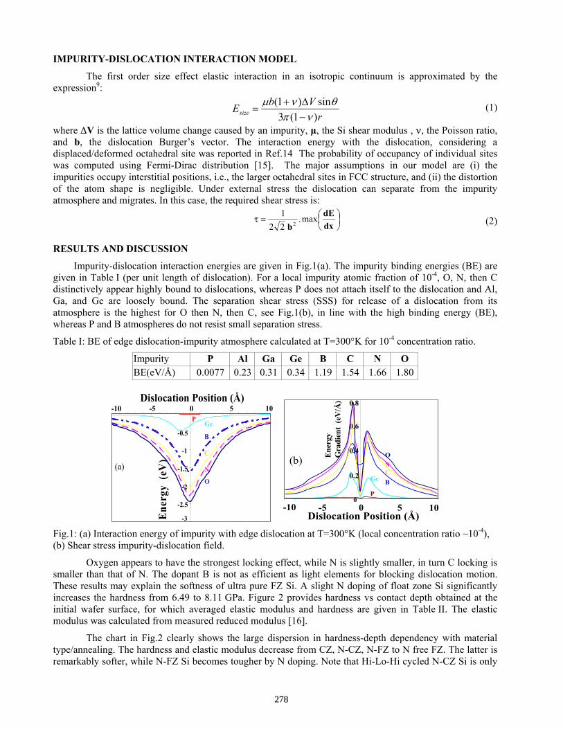
IMPURITY-DISLOCATION INTERACTION MODEL
The first order size effect elastic interaction in an isotropic continuum is approximated by the expression9:
rVbEsize )1(3
sin)1(νπ
θνµ−∆+
= (1)
where ∆V is the lattice volume change caused by an impurity, µ, the Si shear modulus , ν, the Poisson ratio, and b, the dislocation Burger’s vector. The interaction energy with the dislocation, considering a displaced/deformed octahedral site was reported in Ref.14 The probability of occupancy of individual sites was computed using Fermi-Dirac distribution [15]. The major assumptions in our model are (i) the impurities occupy interstitial positions, i.e., the larger octahedral sites in FCC structure, and (ii) the distortion of the atom shape is negligible. Under external stress the dislocation can separate from the impurity atmosphere and migrates. In this case, the required shear stress is:
=
dxdE
b max.
221
2τ (2)
RESULTS AND DISCUSSION
Impurity-dislocation interaction energies are given in Fig.1(a). The impurity binding energies (BE) are given in Table I (per unit length of dislocation). For a local impurity atomic fraction of 10-4, O, N, then C distinctively appear highly bound to dislocations, whereas P does not attach itself to the dislocation and Al, Ga, and Ge are loosely bound. The separation shear stress (SSS) for release of a dislocation from its atmosphere is the highest for O then N, then C, see Fig.1(b), in line with the high binding energy (BE), whereas P and B atmospheres do not resist small separation stress.
Table I: BE of edge dislocation-impurity atmosphere calculated at T=300°K for 10-4 concentration ratio.
Impurity P Al Ga Ge B C N O BE(eV/Å) 0.0077 0.23 0.31 0.34 1.19 1.54 1.66 1.80
(a)
Ge
B C N
O
-3 -2.5
-2 -1.5
-1 -0.5
-10 -5 0 5 10Dislocation Position (Å)
Ene
rgy
(eV
)
P
(b)Ge P
O
N C
B
0
0.2
0.4
0.6
0.8
-10 -5 0 5 10 Dislocation Position (Å)
Ene
rgy
G
radi
ent
(eV
/Å)
Fig.1: (a) Interaction energy of impurity with edge dislocation at T=300°K (local concentration ratio ~10-4), (b) Shear stress impurity-dislocation field.
Oxygen appears to have the strongest locking effect, while N is slightly smaller, in turn C locking is smaller than that of N. The dopant B is not as efficient as light elements for blocking dislocation motion. These results may explain the softness of ultra pure FZ Si. A slight N doping of float zone Si significantly increases the hardness from 6.49 to 8.11 GPa. Figure 2 provides hardness vs contact depth obtained at the initial wafer surface, for which averaged elastic modulus and hardness are given in Table II. The elastic modulus was calculated from measured reduced modulus [16].
The chart in Fig.2 clearly shows the large dispersion in hardness-depth dependency with material type/annealing. The hardness and elastic modulus decrease from CZ, N-CZ, N-FZ to N free FZ. The latter is remarkably softer, while N-FZ Si becomes tougher by N doping. Note that Hi-Lo-Hi cycled N-CZ Si is only
278

slightly softer than Lo-Hi treated CZ. This is likely to be due to the difference in active species type in regard to dislocation locking. In addition, precipitate composition and size are different. It was demonstrated that in annealed N-CZ Si wafers, O precipitates possess a fair amount of N, particularly at the precipitate interface where a 3 nm thick oxy-nitride shell is observed [13].
Table II: Averaged data for initial wafer surfaces (Berkovitch indenter, 5 mN, trapezoidal load function).
Samples <Depth> (nm) < E > (GPa) <H> (GPa)FZ 151.4 103.78 6.49 N-FZ 134.2 181.87 8.11 N-CZ (Hi-Lo-Hi 114.4 189.2 10.8 CZ (Lo-Hi) 111.9 201.23 11.29
It is worth noting that, while the precipitate density is low for N-free low-O CZ Si, much higher concentration of small O precipitates is detected in N-CZ. In addition, with the 2% and 18% N in the center and in the shell, respectively, [13] precipitates are harder (hardness of silicon nitride is 18.6 GPa, see Table III). These features are expected to increase the resistance of precipitate to the shear that may be caused by a moving dislocation, thus results in dislocation locking enhancement, and an increase of material resistance to breakage. Both allow a higher contribution of precipitates to the hardness. Table IV summarizes averaged data obtained from indentation grids in the DZ and in the bulk, using a cross-section Lo-Hi cycled N-CZ sample. Note that:
1. the DZ appears softer than the bulk:11.5±1.0 vs. 12.3±0.9GPa, measured with the same load and tip,
2. the hardness of Hi-Lo-Hi treated N-CZ sample done right at the wafer initial surface, which is 10.8±0.1GPa, see Table II, is close to that measured at 2 µm (Region II), 10.7±1.5GPa, see Table IV.
The lower hardness and modulus found in the DZ are due to lower O, N, and precipitate concentrations, which confirms again the effects of these species on dislocation locking during indentation. The ratios of separation shear stress and dislocation BE to nitrogen over oxygen, are in line with the ratio of measured hardness of N-FZ and CZ over FZ. It is worth noting that heavily boron doped silicon has a very low hardness of
Table III: Published silicon, silicon nitride, and silicon dioxide mechanical properties. VH: Vickers Hardness, KH: Knoop Hardness, Y: Young's Modulus.
Material Property Test Ref.H: 13 GPa Nano indentation, load= 0.2mN, depth= 24nm. Silicon <100> CZ B lightly
doped CZ (1.7x1015cm-3) H: 11.9 GPa Nano indentation, load= 15 mN, depth= 267 nm. H: 5.1 GPa Nano-indentation, load= 0.2 mN depth= 44 nm. Silicon<100>, CZ B
heavily doped (7x1019cm-3) H: 8.7 GPa Nano indentation, load= 15 mN, depth= 318 nm.
17
Silicon <111> H: 11.7 GPa Nanotribology by AFM/FFM, load= 100 µN scan size= 500X500 nm2
C+ implanted silicon <111> H: 18.6 GPa Nanoindentation, load= 100 µN
18
VH: 8.15-19.36 GPa Vickers 19 Y: 250-325.04 GPa material hot pressed, at T=20 C Y: 195.05-315.05 GPa Ceramic, sintered , at T=20 C
Ceramic Si3N4 (bulk)
Y: 100.02-220.02 GPa Ceramic, reaction sintered, at T=20 C
20
KH: 7.1-7.9 GPa Knoop, 100g, parallel to optical axis Ceramic SiO2 (bulk) VH: 11.03-12.6 GPa Vickers, 500g, parallel to optical axis
21
6
7
8
9
10
1112
110 120 130 140 150Contact Depth (nm)
Har
dnes
s (G
Pa)
Hi-Lo-Hi, N-CZ
‘as grown’ N-FZ
‘as grown’ FZ
Lo-Hi, CZ
Berkovitch tip Load: 5mN
‘as grown’ [111] CZ (Ref. 11)
Fig. 2: Hardness of Si at wafer surface (Region I in N-CZ). For the ‘as grown’ N-FZ silicon, three samples have been used, and each point is an average over a small grid of 3x3 indents.
279

5-8 GPa, see Table III. We propose that B reduces oxygen effects on hardness; in addition, B does not lock dislocations, as demonstrated by the low values of its BE and separation shear stress. In contrast, heavily C doped silicon (implantation) increases dramatically the hardness to 18.6 GPa, see Table III; this is in argument with the predicted behavior of C in regard to dislocation locking.
Table IV: Data from various indentation grids (49 points) on the cross-section of N-CZ sample. d: distance from wafer surface, B: Berkovitch, N: Northstar indenter.
Region
d (µm)
Tip Load (µN)
<Depth>±σ (nm)
<E> (GPa)
<H> ±σ (GPa)
2 N 175 30.0±3.3 169.7 10.7±1.5 II 5 B 400 21.5±1.5 199.7 11.5±1.0
400 20.5±1.2 205.7 12.3±0.9 III 150 B 5000 112.0±1.4 208.5 11.3±.25
SUMMARY
Silicon hardness and elastic modulus significantly vary with O and N contents. CZ Si appeared about twice as hard as pure FZ Si. Doping FZ Si with N or C significantly increases the hardness. Silicon is soften by heavily doping it with B, while this dopant reduces the O effects on silicon hardness. The N and O denuded zone in annealed wafers is softer than the bulk region. The effects of N and O on the hardness strongly correlates with their locking effects on edge dislocations. O, N, and C appear to be localized at the core of edge dislocations. The BE of these impurities is 200 times higher than phosphor. Similarly, the dislocation-impurity separation shear stress is higher for O, N, then C than all other impurities.
ACKNOWLEDGEMENTS
This work is supported by the National Renewable Energy Laboratory, NREL grant # AAT-2-31605-05 and NSF trough SiWEDS grant EEC-0308883. References [1] A. Blakers, K.Weber, M.Stocks, J.Babei, V.Everett, M.Kerr, and P.Verlinden, Sliver Solar Cells, 13th Workshop on
Crystalline Silicon Solar Cell Materials and Process, Vail, Co, Aug. 10-13, 2003. P.J.Verlinden, A.W.Blakers, K.J. Weber, V. Everett, M. J. Kerr, M. F. Stuckings, D. Gordeev, and M. J. Stocks, Sliver Solar Cells: A New Thin Crystalline Silicon Photovoltaic Technology, PVSEC-14, Jan. 2004.
[2] R.B. Bergmann, Crystalline Si Thin-Film Solar Cells: a Review, Appl. Phys. A 69, 187–194 (1999). [3] T. Abe, K. Kikuchi, S. Shira, and S. Muraoka, in “Semiconductor Silicon/1981”, H. R. Huff, J. Kriegler and Y.
Takeishi, eds., p.54, Softbound Symp. Serv. Electrochem. Soc., Pennington, New Jersey, 1981. [4] K. Sumino, I. Yonenaga, M. Imai and T. Abe, J. Appl. Phys. 54, 5016 (1983). [5] A. Karoui, G. A. Rozgonyi, “Optimization of Silicon Crystal Growth and Wafer Processing for High Efficiency and
High Mechanical Yield”, Ann. Rep.1 of Project: NREL, AAT-2-31605-05, Nov. 2002. [6] T. F. Cizek, T. H. Wang, R. W. Burrows, T. Bekkedahl, M. I. Symko, J. D. Webb. Solar Energy Materials and Solar
Cells 41/42, 61-70 (1996). [7] A. w. Cochardt, Acta Metall. 3, (1955) [8] D. M. Barnett and W. D. Nix, Acta Metall. 2, (1955). [9] A.H.Cottrel, B.A. Bilby Proc. Phys. Soc. A, 62, 49 (1949). [10] R. A. Johnson, J. Appl. Phys., 50, 1263 (1979). [11] J. Tersoff, Phys. Rev. B, 39(8), 5566 (1989). [12] A.Karoui, Atomistic Modeling of Impurity Atmospheres in Silicon and Dislocation Locking Effects, Symposium(P),
MRS Spring Meeting, San Francisco, Apr.12-16, 2004. [13] A. Karoui et al., J. Appl. Phys., Aug. 15, 2004. [14] A.Nandekar, R. A. Johnson, Acta Metall. 30, 2055 (1982). [15] R. A. Johnson, Phys. Rev. B, 24 (12), 7383 (1981). [16] W. C. Oliver, G. M. Pharr, J. Mat. Res. 7(6), 1564 (1992). [17] Bharat Bhushan, Xiaodong Li, J. Mater. Res, 12,(1), (1997), p.59 [18] Bharat Bhushan, IEEE MEMS Workshop, SanDiego, CA, Feb. 1996, p.91-p.97 (1996). [19] CRC Materials Science and Engineering Handbook, p.473 [20] ibid, p.509 [21] ibid, p.474

F1147-E(05/2004)
REPORT DOCUMENTATION PAGE Form Approved OMB No. 0704-0188
The public reporting burden for this collection of information is estimated to average 1 hour per response, including the time for reviewing instructions, searching existing data sources, gathering and maintaining the data needed, and completing and reviewing the collection of information. Send comments regarding this burden estimate or any other aspect of this collection of information, including suggestions for reducing the burden, to Department of Defense, Executive Services and Communications Directorate (0704-0188). Respondents should be aware that notwithstanding any other provision of law, no person shall be subject to any penalty for failing to comply with a collection of information if it does not display a currently valid OMB control number. PLEASE DO NOT RETURN YOUR FORM TO THE ABOVE ORGANIZATION. 1. REPORT DATE (DD-MM-YYYY)
August 2004 2. REPORT TYPE
Conference Proceedings (Workshop) 3. DATES COVERED (From - To)
8-11 August 2004 5a. CONTRACT NUMBER
DE-AC36-99-GO10337 5b. GRANT NUMBER
4. TITLE AND SUBTITLE 14th Workshop on Crystalline Silicon Solar Cells & Modules: Materials and Processes, Extended Abstracts and Papers
5c. PROGRAM ELEMENT NUMBER
5d. PROJECT NUMBER NREL/BK-520-36622
5e. TASK NUMBER WO97D999
6. AUTHOR(S) B.L. Sopori, Workshop Chairman/Editor
5f. WORK UNIT NUMBER
7. PERFORMING ORGANIZATION NAME(S) AND ADDRESS(ES) National Renewable Energy Laboratory 1617 Cole Blvd. Golden, CO 80401-3393
8. PERFORMING ORGANIZATION REPORT NUMBER NREL/BK-520-36622
10. SPONSOR/MONITOR'S ACRONYM(S) NREL
9. SPONSORING/MONITORING AGENCY NAME(S) AND ADDRESS(ES)
11. SPONSORING/MONITORING AGENCY REPORT NUMBER
12. DISTRIBUTION AVAILABILITY STATEMENT National Technical Information Service U.S. Department of Commerce 5285 Port Royal Road Springfield, VA 22161
13. SUPPLEMENTARY NOTES
14. ABSTRACT (Maximum 200 Words) The 14th Workshop will provide a forum for an informal exchange of technical and scientific information between international researchers in the photovoltaic and relevant non-photovoltaic fields. It will offer an excellent opportunity for researchers in private industry and at universities to prioritize mutual needs for future collaborative research. The workshop is intended to address the fundamental properties of PV silicon, new solar cell designs, advanced solar cell processing techniques, and cell-related module issues. A combination of oral presentations by invited speakers, poster sessions, and discussion sessions will review recent advances in crystal growth, new cell designs, new processes and process characterization techniques, cell fabrication approaches suitable for future manufacturing demands, and solar cell encapsulation. This year's theme, "Crystalline Si Solar Cells: Leapfrogging the Barriers," reflects the continued success of crystalline Si PV in overcoming technological barriers to improve solar cell performance and lower the cost of Si PV. The workshop will consist of presentations by invited speakers, followed by discussion sessions. In addition, there will be two poster sessions presenting the latest research and development results. Some presentations will address recent technologies in the microelectronics field that may have a direct bearing on PV. The sessions will include: Advances in crystal growth and material issues; Impurities and defects; Dynamics during device processing; Passivation, High-efficiency Si solar cells; Advanced processing; Thin Si solar cells; and Solar cell reliability and module issues. 15. SUBJECT TERMS
photovoltaics; solar cells; crystalline silicon; materials and processes; module; impurities, device process; crystal growth; defect; passivation; microelectronics; advanced processing;
16. SECURITY CLASSIFICATION OF: 19a. NAME OF RESPONSIBLE PERSON a. REPORT
Unclassified b. ABSTRACT Unclassified
c. THIS PAGE Unclassified
17. LIMITATION OF ABSTRACT
UL
18. NUMBER OF PAGES
19b. TELEPONE NUMBER (Include area code)
Standard Form 298 (Rev. 8/98) Prescribed by ANSI Std. Z39.18