15 w, 12 v output, isolated flyback converter using ... · january 2016 docid028844 rev 1 1/18...
TRANSCRIPT

January 2016 DocID028844 Rev 1 1/18
www.st.com
AN4812 Application note
15 W, 12 V output, isolated flyback converter using Viper35HD device from the VIPer™ Plus family of high voltage converters
Introduction This document describes the STEVAL-ISA171V1 implementing a 15 W wide range SMPS based on the new Viper35HD HV converter in the VIPer Plus quasi-resonant range of devices.
The STEVAL-ISA171V1 is designed to optimize efficiency and electrical performance, while restricting overall board dimensions.

Contents AN4812
2/18 DocID028844 Rev 1
Contents
1 Test board: Design and evaluation ............................................... 3
1.1 Output voltage characteristic ............................................................ 7
1.2 Efficiency and light load measurements ........................................... 7
1.3 Typical board waveforms ................................................................. 8
2 Conducted noise measurements ................................................ 14
3 Conclusions .................................................................................. 15
4 Demonstration tools and documentation ................................... 16
5 Revision history ........................................................................... 17
AN4812 Test board: Design and evaluation
DocID028844 Rev 1 3/18
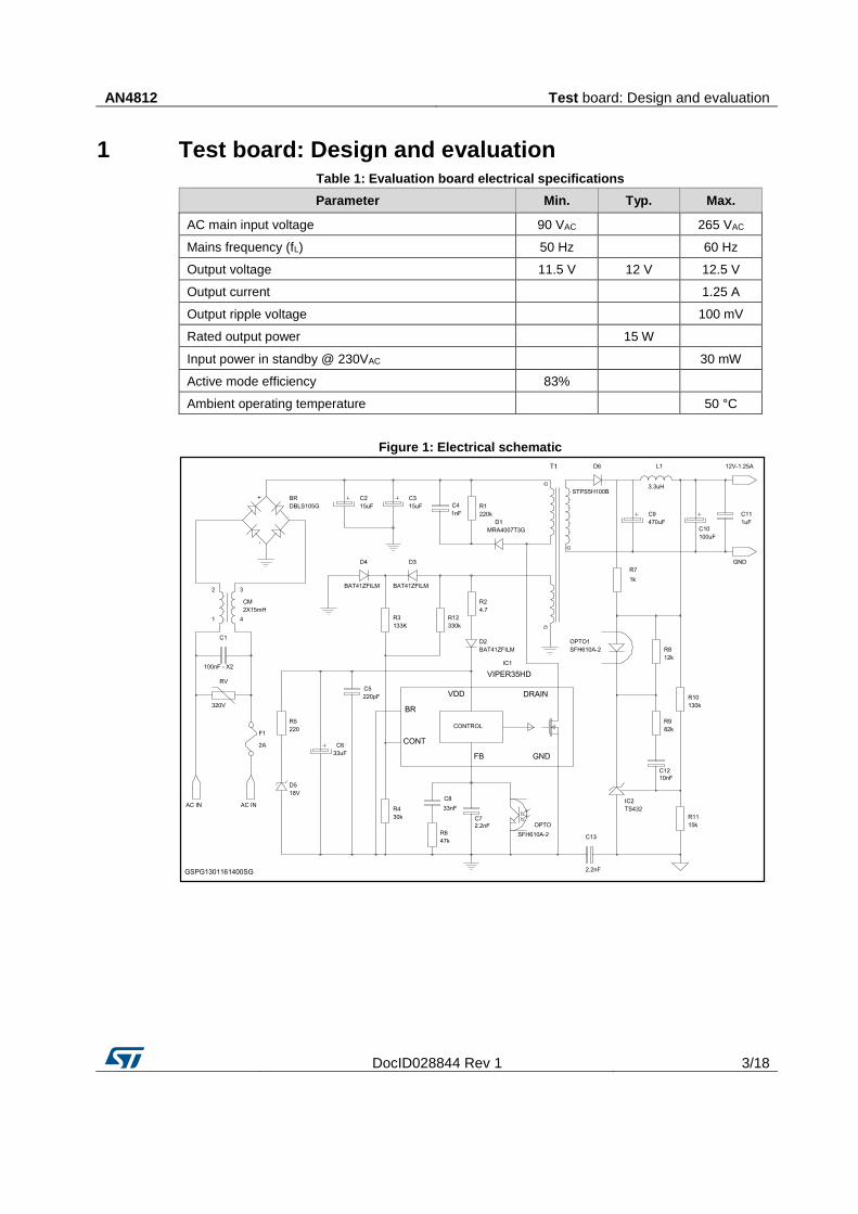
1 Test board: Design and evaluation Table 1: Evaluation board electrical specifications
Parameter Min. Typ. Max.
AC main input voltage 90 VAC 265 VAC
Mains frequency (fL) 50 Hz 60 Hz
Output voltage 11.5 V 12 V 12.5 V
Output current 1.25 A
Output ripple voltage 100 mV
Rated output power 15 W
Input power in standby @ 230VAC 30 mW
Active mode efficiency 83%
Ambient operating temperature 50 °C
Figure 1: Electrical schematic

Test board: Design and evaluation AN4812
4/18 DocID028844 Rev 1
Figure 2: Demo board picture: (30 x 72 mm.) max
Table 2: VIPer35H demonstration board bill of material
Reference Part Manufacturer Description
R1 ERJ-P08J224V Panasonic 220kΩ±5% - 0.33W - 200V
R2 ERJ3RQF4R7V Panasonic 4.7Ω±1% - 0.1W
R3 CRCW0603133KFKEA Vishay 133kΩ±1% - 0.1W
R4 ERJP03F3002V Panasonic 30kΩ±1% - 0.1W
R5 ERJT06J221V Panasonic 220Ω±5% - 0.25W
R6 ERJ-3EKF4702V Panasonic 47kΩ±1% - 0.1W
R7 ERJ3GEYJ102V Panasonic 1kΩ±5% - 0.1W
R8 ERJ3GEYJ123V Panasonic 12kΩ±5% - 0.1W
R9 ERJ3GEYJ823V Panasonic 82kΩ±5% - 0.1W
R10 ERJP03F1203V Panasonic 130kΩ±1% - 0.2W
R11 ERJP03F1502V Panasonic 15kΩ±1% - 0.2W
R12 ERJ3RED3303V Panasonic 330kΩ±1% - 0.1W
C1 ECQUAAF104M Panasonic 100nF-275V X2 cap
C2 UVC2G150MPD Nichicon Elcap 15uF-400V
C3 UVC2G150MPD Nichicon Elcap 15uF-400V
C4 C3216C0G2J102JT TDK MLCC capacitor 1nF-630V
C5 GRM188R71H221KA01D Murata MLCC capacitor 220pF-16V
C6 35YXM33MEFC5X11 Rubycon Elcap 33uF-35V
C7 GRM1885C1H222FA01D Murata MLCC capacitor 2.2nF-50V
C8 GRM188R71H333KA61D Murata MLCC capacitor 33nF-16V
C9 25ZLJ470M10X12.5 Rubycon Elcap 470uF-25V
C10 25YXJ100M5X11 Rubycon Elcap 100uF-25V
C11 GRM188C81E105KAADD Murata MLCC capacitor 1uF-25V
C12 GRM188R71H103KA01D Murata MLCC capacitor 10nF-50V

AN4812 Test board: Design and evaluation
DocID028844 Rev 1 5/18
Reference Part Manufacturer Description
C13 DE2E3KY222MA2BM01 Murata Ceramic X1/Y1 cap. 2.2nF
250Vac
D1 MRA4007T3G ON Semiconductor 1A-1000V Power rectifier diode
D2 BAT41ZFILM STMictroelectronics Signal schottky 0.15A-100V
D3 BAT41ZFILM STMictroelectronics Signal schottky 0.15A-100V
D4 BAT41ZFILM STMictroelectronics Signal schottky 0.15A-100V
D5 MMSZ5248B-V-GS08 Vishay Zener diode 18V
D6 STPS5H100B STMictroelectronics Power Schottky 100V-5A
L1 SD43-332ML Coilcraft 3.3uH
CM 744821120 Wurth Elektronik 20mH CM CHOKE
IC1 VIPer35HD STMicroelectronics Offline HV converter
OPT SFH6106-2T Vishay Optocoupler
REF TS432ILT STMicroelectronics Reference
T1 750370228 Rev. 6A Wurth Elektronik EE20/10/6 Flyback transformer
RV B72210S0321K101 EPCOS MOV
RB DBLS105G Taiwan Semicond. Bridge rectifier
FS SS-5H-2-5A-BK Cooper Bussmann 2.5A fuse
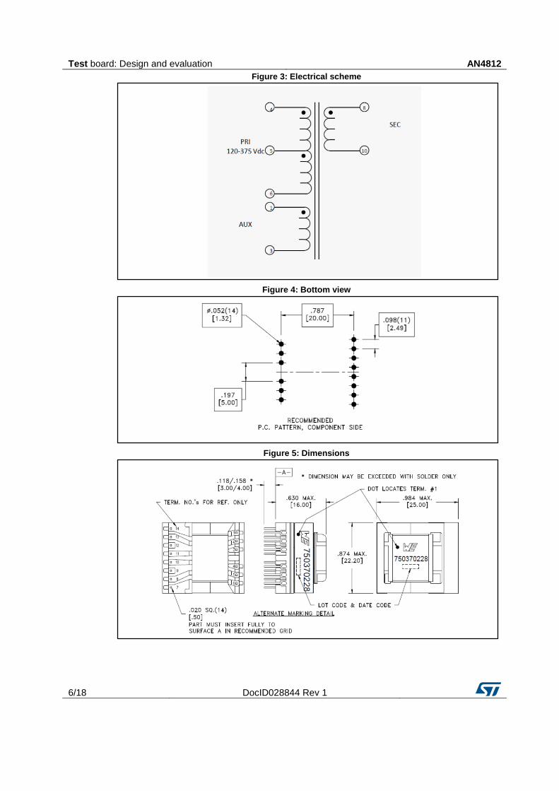
Table 3: Transformer characteristics
Type Characteristics
Manufacturer Wurth Elektonik
Part number 750370228 Rev. 6A
Core EE20/10/6
Ferrite TBD
Primary Inductance 1.5 mH ±10%
Leakage inductance 45 µH max
Primary turns (N1+N3) 168
Secondary turns (N2) 21
Auxiliary turns (N4) 21
Test board: Design and evaluation AN4812
6/18 DocID028844 Rev 1
Figure 3: Electrical scheme
Figure 4: Bottom view
Figure 5: Dimensions
AN4812 Test board: Design and evaluation
DocID028844 Rev 1 7/18
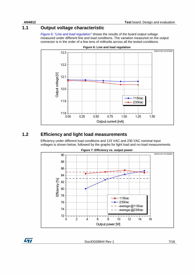
1.1 Output voltage characteristic
Figure 6: "Line and load regulation" shows the results of the board output voltage measured under different line and load conditions. The variation measured on the output connector is in the order of a few tens of millivolts across all the tested conditions.
Figure 6: Line and load regulation
1.2 Efficiency and light load measurements
Efficiency under different load conditions and 115 VAC and 230 VAC nominal input voltages is shown below, followed by the graphs for light load and no-load measurements.
Figure 7: Efficiency vs. output power

Test board: Design and evaluation AN4812
8/18 DocID028844 Rev 1
Table 4: Efficiency at 10% of the rated output load
Input voltage Efficiency
115 VAC 81.70 %
230 VAC 77.16 %
Figure 8: No load consumption vs. input voltage
Figure 9: Light load consumptions at different output powers
1.3 Typical board waveforms
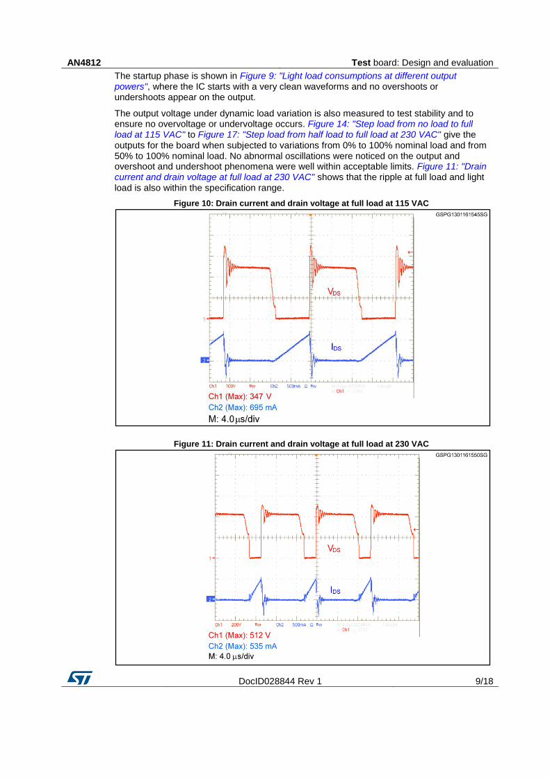
Drain voltage and current waveforms are given at nominal input voltages and full load in Figure 10: "Drain current and drain voltage at full load at 115 VAC".
AN4812 Test board: Design and evaluation
DocID028844 Rev 1 9/18
The startup phase is shown in Figure 9: "Light load consumptions at different output powers", where the IC starts with a very clean waveforms and no overshoots or undershoots appear on the output.
The output voltage under dynamic load variation is also measured to test stability and to ensure no overvoltage or undervoltage occurs. Figure 14: "Step load from no load to full load at 115 VAC" to Figure 17: "Step load from half load to full load at 230 VAC" give the outputs for the board when subjected to variations from 0% to 100% nominal load and from 50% to 100% nominal load. No abnormal oscillations were noticed on the output and overshoot and undershoot phenomena were well within acceptable limits. Figure 11: "Drain current and drain voltage at full load at 230 VAC" shows that the ripple at full load and light load is also within the specification range.
Figure 10: Drain current and drain voltage at full load at 115 VAC
Figure 11: Drain current and drain voltage at full load at 230 VAC

Test board: Design and evaluation AN4812
10/18 DocID028844 Rev 1
Figure 12: Startup at full load at 115 VAC
Figure 13: Startup at full load at 230 VAC

AN4812 Test board: Design and evaluation
DocID028844 Rev 1 11/18
Figure 14: Step load from no load to full load at 115 VAC
Figure 15: Step load from no load to full load at 230 VAC

Test board: Design and evaluation AN4812
12/18 DocID028844 Rev 1
Figure 16: Step load from half load to full load at 115 VAC
Figure 17: Step load from half load to full load at 230 VAC

AN4812 Test board: Design and evaluation
DocID028844 Rev 1 13/18
Figure 18: Output voltage ripple at no load
Figure 19: Output voltage ripple at full load
Conducted noise measurements AN4812
14/18 DocID028844 Rev 1
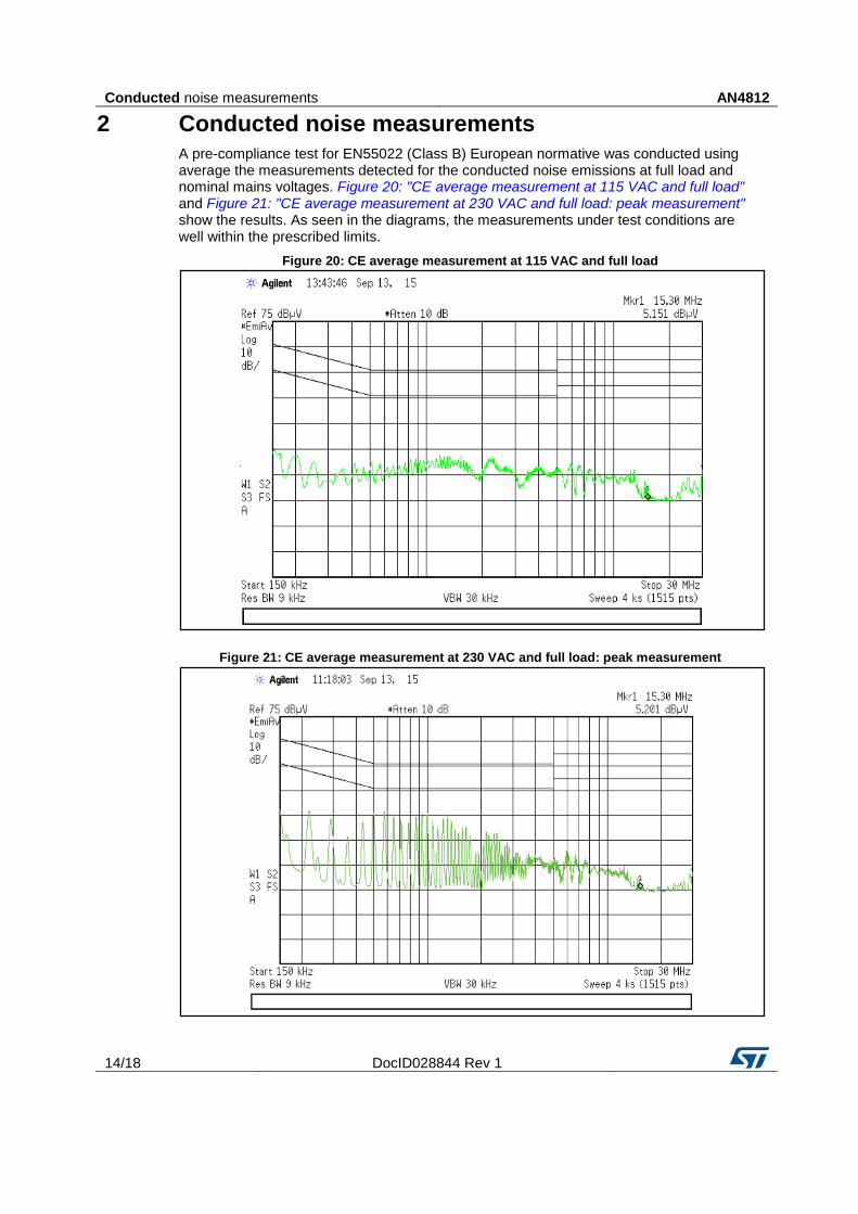
2 Conducted noise measurements
A pre-compliance test for EN55022 (Class B) European normative was conducted using average the measurements detected for the conducted noise emissions at full load and nominal mains voltages. Figure 20: "CE average measurement at 115 VAC and full load" and Figure 21: "CE average measurement at 230 VAC and full load: peak measurement" show the results. As seen in the diagrams, the measurements under test conditions are well within the prescribed limits.
Figure 20: CE average measurement at 115 VAC and full load
Figure 21: CE average measurement at 230 VAC and full load: peak measurement

AN4812 Conclusions
DocID028844 Rev 1 15/18
3 Conclusions
The results presented here for a 15 W wide range single output flyback converter using the new VIPer35HD demonstrate that these power supply units are especially suitable for applications requiring an external adapter or auxiliary power supply able to deliver high performance while maintaining a relatively small dimensions.

Demonstration tools and documentation AN4812
16/18 DocID028844 Rev 1
4 Demonstration tools and documentation
The VIPer35HD demonstration board order code is STEVAL-SA171V1. Consult the VIPer35 datasheet at www.st.com for further information.

AN4812 Revision history
DocID028844 Rev 1 17/18
5 Revision history Table 5: Document revision history
Date Revision Changes
19-Jan-2016 1 Initial release.
AN4812
18/18 DocID028844 Rev 1
IMPORTANT NOTICE – PLEASE READ CAREFULLY
STMicroelectronics NV and its subsidiaries (“ST”) reserve the right to make changes, corrections, enhancements, modifications , and improvements to ST products and/or to this document at any time without notice. Purchasers should obtain the latest relevant information on ST products before placing orders. ST products are sold pursuant to ST’s terms and conditions of sale in place at the time of order acknowledgement.
Purchasers are solely responsible for the choice, selection, and use of ST products and ST assumes no liability for application assistance or the design of Purchasers’ products.
No license, express or implied, to any intellectual property right is granted by ST herein.
Resale of ST products with provisions different from the information set forth herein shall void any warranty granted by ST for such product.
ST and the ST logo are trademarks of ST. All other product or service names are the property of their respective owners.
Information in this document supersedes and replaces information previously supplied in any prior versions of this document.
© 2016 STMicroelectronics – All rights reserved