1502c metallic time-domain reflectometer service manualdownload.tek.com/manual/070716804.pdf ·...
TRANSCRIPT

Service Manual
1502CMetallic Time-Domain Reflectometer
070-7168-04
This document applies to firmware version 5.02and above.
WarningThe servicing instructions are for use by qualifiedpersonnel only. To avoid personal injury, do notperform any servicing unless you are qualified todo so. Refer to all safety summaries prior toperforming service.
www.tektronix.com

Copyright Tektronix, Inc. All rights reserved.
Tektronix products are covered by U.S. and foreign patents, issued and pending. Information in this publication supercedesthat in all previously published material. Specifications and price change privileges reserved.
Tektronix, Inc., P.O. Box 500, Beaverton, OR 97077
TEKTRONIX and TEK are registered trademarks of Tektronix, Inc.

WARRANTY
Tektronix warrants that the products that it manufactures and sells will be free from defects in materials and workmanshipfor a period of one (1) year from the date of shipment. If a product proves defective during this warranty period, Tektronix,at its option, either will repair the defective product without charge for parts and labor, or will provide a replacement inexchange for the defective product.
In order to obtain service under this warranty, Customer must notify Tektronix of the defect before the expiration of thewarranty period and make suitable arrangements for the performance of service. Customer shall be responsible forpackaging and shipping the defective product to the service center designated by Tektronix, with shipping charges prepaid.Tektronix shall pay for the return of the product to Customer if the shipment is to a location within the country in which theTektronix service center is located. Customer shall be responsible for paying all shipping charges, duties, taxes, and anyother charges for products returned to any other locations.
This warranty shall not apply to any defect, failure or damage caused by improper use or improper or inadequatemaintenance and care. Tektronix shall not be obligated to furnish service under this warranty a) to repair damage resultingfrom attempts by personnel other than Tektronix representatives to install, repair or service the product; b) to repairdamage resulting from improper use or connection to incompatible equipment; c) to repair any damage or malfunctioncaused by the use of non-Tektronix supplies; or d) to service a product that has been modified or integrated with otherproducts when the effect of such modification or integration increases the time or difficulty of servicing the product.
THIS WARRANTY IS GIVEN BY TEKTRONIX IN LIEU OF ANY OTHER WARRANTIES, EXPRESS ORIMPLIED. TEKTRONIX AND ITS VENDORS DISCLAIM ANY IMPLIED WARRANTIES OFMERCHANTABILITY OR FITNESS FOR A PARTICULAR PURPOSE. TEKTRONIX’ RESPONSIBILITY TOREPAIR OR REPLACE DEFECTIVE PRODUCTS IS THE SOLE AND EXCLUSIVE REMEDY PROVIDED TOTHE CUSTOMER FOR BREACH OF THIS WARRANTY. TEKTRONIX AND ITS VENDORS WILL NOT BELIABLE FOR ANY INDIRECT, SPECIAL, INCIDENTAL, OR CONSEQUENTIAL DAMAGES IRRESPECTIVEOF WHETHER TEKTRONIX OR THE VENDOR HAS ADVANCE NOTICE OF THE POSSIBILITY OF SUCHDAMAGES.


1502C MTDR Service Manual i
Table of Contents
General Safety Summary xi. . . . . . . . . . . . . . . . . . . . . . . . . . . . . . . . . . . . . . . . . . . Service Safety Summary xiii. . . . . . . . . . . . . . . . . . . . . . . . . . . . . . . . . . . . . . . . . . .
General Information xv. . . . . . . . . . . . . . . . . . . . . . . . . . . . . . . . . . . . . . . . Installation and Repacking xvi. . . . . . . . . . . . . . . . . . . . . . . . . . . . . . . . . . . . . . . . . . Contacting Tektronix xviii. . . . . . . . . . . . . . . . . . . . . . . . . . . . . . . . . . . . . . . . . . . . . .
Operating InstructionsOperating Instructions 1–1. . . . . . . . . . . . . . . . . . . . . . . . . . . . . . . . . . . . . . Overview 1–1. . . . . . . . . . . . . . . . . . . . . . . . . . . . . . . . . . . . . . . . . . . . . . . . . . . . . . . Preparing to Use the 1502C 1–5. . . . . . . . . . . . . . . . . . . . . . . . . . . . . . . . . . . . . . . . . Display 1–6. . . . . . . . . . . . . . . . . . . . . . . . . . . . . . . . . . . . . . . . . . . . . . . . . . . . . . . . . Front-Panel Controls 1–6. . . . . . . . . . . . . . . . . . . . . . . . . . . . . . . . . . . . . . . . . . . . . . Menu Selections 1–7. . . . . . . . . . . . . . . . . . . . . . . . . . . . . . . . . . . . . . . . . . . . . . . . . . Test Preparations 1–11. . . . . . . . . . . . . . . . . . . . . . . . . . . . . . . . . . . . . . . . . . . . . . . . . Cable Test Procedure 1–13. . . . . . . . . . . . . . . . . . . . . . . . . . . . . . . . . . . . . . . . . . . . . . Additional Features (Menu Selected) 1–26. . . . . . . . . . . . . . . . . . . . . . . . . . . . . . . . . .
Operator Performance ChecksOperator Performance Checks 2–1. . . . . . . . . . . . . . . . . . . . . . . . . . . . . . .
SpecificationsSpecifications 3–1. . . . . . . . . . . . . . . . . . . . . . . . . . . . . . . . . . . . . . . . . . . . . . Electrical Characteristics 3–1. . . . . . . . . . . . . . . . . . . . . . . . . . . . . . . . . . . . . . . . . . . Environmental Characteristics 3–3. . . . . . . . . . . . . . . . . . . . . . . . . . . . . . . . . . . . . . . Certifications and Compliances 3–4. . . . . . . . . . . . . . . . . . . . . . . . . . . . . . . . . . . . . . Physical Characteristics 3–5. . . . . . . . . . . . . . . . . . . . . . . . . . . . . . . . . . . . . . . . . . . .
Options and Accessories
Options and Accessories 4–1. . . . . . . . . . . . . . . . . . . . . . . . . . . . . . . . . . . . . Option 04: YT–1 Chart Recorder 4–1. . . . . . . . . . . . . . . . . . . . . . . . . . . . . . . . . . . . . Option 05: Metric Default 4–1. . . . . . . . . . . . . . . . . . . . . . . . . . . . . . . . . . . . . . . . . . Option 07: YT–1S Chart Recorder 4–1. . . . . . . . . . . . . . . . . . . . . . . . . . . . . . . . . . . Power Cord Options 4–1. . . . . . . . . . . . . . . . . . . . . . . . . . . . . . . . . . . . . . . . . . . . . . . Accessories 4–2. . . . . . . . . . . . . . . . . . . . . . . . . . . . . . . . . . . . . . . . . . . . . . . . . . . . . .
Circuit DescriptionsCircuit Descriptions 5–1. . . . . . . . . . . . . . . . . . . . . . . . . . . . . . . . . . . . . . . . . Introduction 5–1. . . . . . . . . . . . . . . . . . . . . . . . . . . . . . . . . . . . . . . . . . . . . . . . . . . . . Power Supply 5–4. . . . . . . . . . . . . . . . . . . . . . . . . . . . . . . . . . . . . . . . . . . . . . . . . . . .

Table of Contents
ii 1502C MTDR Service Manual
Processor System 5–7. . . . . . . . . . . . . . . . . . . . . . . . . . . . . . . . . . . . . . . . . . . . . . . . . Option Port Interface 5–10. . . . . . . . . . . . . . . . . . . . . . . . . . . . . . . . . . . . . . . . . . . . . . Video Processor 5–13. . . . . . . . . . . . . . . . . . . . . . . . . . . . . . . . . . . . . . . . . . . . . . . . . . Timebase 5–15. . . . . . . . . . . . . . . . . . . . . . . . . . . . . . . . . . . . . . . . . . . . . . . . . . . . . . . Driver/Sampler 5–23. . . . . . . . . . . . . . . . . . . . . . . . . . . . . . . . . . . . . . . . . . . . . . . . . . . Front Panel 5–25. . . . . . . . . . . . . . . . . . . . . . . . . . . . . . . . . . . . . . . . . . . . . . . . . . . . . . Display Module 5–28. . . . . . . . . . . . . . . . . . . . . . . . . . . . . . . . . . . . . . . . . . . . . . . . . .
Calibration and AdjustmentsCalibration 6–1. . . . . . . . . . . . . . . . . . . . . . . . . . . . . . . . . . . . . . . . . . . . . . . . Introduction 6–1. . . . . . . . . . . . . . . . . . . . . . . . . . . . . . . . . . . . . . . . . . . . . . . . . . . . .
Calibration Performance Check 6–1. . . . . . . . . . . . . . . . . . . . . . . . . . . . . . Display Module Check 6–2. . . . . . . . . . . . . . . . . . . . . . . . . . . . . . . . . . . . . . . . . . . . . Front Panel Check 6–4. . . . . . . . . . . . . . . . . . . . . . . . . . . . . . . . . . . . . . . . . . . . . . . . Horizontal Scale (Timebase) Check 6–7. . . . . . . . . . . . . . . . . . . . . . . . . . . . . . . . . . . Zero Offset Check 6–10. . . . . . . . . . . . . . . . . . . . . . . . . . . . . . . . . . . . . . . . . . . . . . . . Vertical Position (Offset) Check 6–12. . . . . . . . . . . . . . . . . . . . . . . . . . . . . . . . . . . . . Noise Check 6–13. . . . . . . . . . . . . . . . . . . . . . . . . . . . . . . . . . . . . . . . . . . . . . . . . . . . . Sampling Efficiency Check 6–15. . . . . . . . . . . . . . . . . . . . . . . . . . . . . . . . . . . . . . . . . Offset/Gain Check 6–16. . . . . . . . . . . . . . . . . . . . . . . . . . . . . . . . . . . . . . . . . . . . . . . . RAM/ROM Check 6–17. . . . . . . . . . . . . . . . . . . . . . . . . . . . . . . . . . . . . . . . . . . . . . . . Aberrations Check 6–17. . . . . . . . . . . . . . . . . . . . . . . . . . . . . . . . . . . . . . . . . . . . . . . . Risetime Check 6–19. . . . . . . . . . . . . . . . . . . . . . . . . . . . . . . . . . . . . . . . . . . . . . . . . . Jitter Check 6–21. . . . . . . . . . . . . . . . . . . . . . . . . . . . . . . . . . . . . . . . . . . . . . . . . . . . . . Option 04/07: YT-1/YT-1S Chart Recorder Check 6–23. . . . . . . . . . . . . . . . . . . . . . . Option 05: Metric Default Check 6–23. . . . . . . . . . . . . . . . . . . . . . . . . . . . . . . . . . . . .
Adjustment Procedures 6–25. . . . . . . . . . . . . . . . . . . . . . . . . . . . . . . . . . . . . . Visual Inspection 6–26. . . . . . . . . . . . . . . . . . . . . . . . . . . . . . . . . . . . . . . . . . . . . . . . . Power Supply Checks and Adjustments 6–26. . . . . . . . . . . . . . . . . . . . . . . . . . . . . . . Main Board ”12 VDC Check and Adjust 6–30. . . . . . . . . . . . . . . . . . . . . . . . . . . . . . . Impedance Check 6–35. . . . . . . . . . . . . . . . . . . . . . . . . . . . . . . . . . . . . . . . . . . . . . . . . LCD Check and Adjustment 6–36. . . . . . . . . . . . . . . . . . . . . . . . . . . . . . . . . . . . . . . . Zero Offset Adjust 6–39. . . . . . . . . . . . . . . . . . . . . . . . . . . . . . . . . . . . . . . . . . . . . . . . After Adjustments are Completed 6–41. . . . . . . . . . . . . . . . . . . . . . . . . . . . . . . . . . . .
MaintenanceMaintenance 7–1. . . . . . . . . . . . . . . . . . . . . . . . . . . . . . . . . . . . . . . . . . . . . . . Introduction 7–1. . . . . . . . . . . . . . . . . . . . . . . . . . . . . . . . . . . . . . . . . . . . . . . . . . . . . Preventive Maintenance 7–1. . . . . . . . . . . . . . . . . . . . . . . . . . . . . . . . . . . . . . . . . . . . Part Removal and Replacement 7–2. . . . . . . . . . . . . . . . . . . . . . . . . . . . . . . . . . . . . . Troubleshooting 7–12. . . . . . . . . . . . . . . . . . . . . . . . . . . . . . . . . . . . . . . . . . . . . . . . . . Control Panel Installation 7–17. . . . . . . . . . . . . . . . . . . . . . . . . . . . . . . . . . . . . . . . . . . Installing the Case Cover Over the Chassis 7–19. . . . . . . . . . . . . . . . . . . . . . . . . . . . .

Table of Contents
1502C MTDR Service Manual iii
Replaceable Electrical PartsReplaceable Electrical Parts 8–1. . . . . . . . . . . . . . . . . . . . . . . . . . . . . . . . . . Parts Ordering Information 8–1. . . . . . . . . . . . . . . . . . . . . . . . . . . . . . . . . . . . . . . . .
DiagramsDiagrams 9–1. . . . . . . . . . . . . . . . . . . . . . . . . . . . . . . . . . . . . . . . . . . . . . . . . General Information 9–1. . . . . . . . . . . . . . . . . . . . . . . . . . . . . . . . . . . . . . . . . . . . . . .
Replaceable Mechanical PartsReplaceable Mechanical Parts 10–1. . . . . . . . . . . . . . . . . . . . . . . . . . . . . . . . Parts Ordering Information 10–1. . . . . . . . . . . . . . . . . . . . . . . . . . . . . . . . . . . . . . . . . Using the Replaceable Mechanical Parts List 10–1. . . . . . . . . . . . . . . . . . . . . . . . . . .
Glossary and Index

Table of Contents
iv 1502C MTDR Service Manual
List of Figures
Figure 1–1: Rear Panel Voltage Selector, Fuse, AC Receptacle 1–1. . . . .
Figure 1–2: Display Showing Low Battery Indication 1–4. . . . . . . . . . . .
Figure 1–3: 1502C Front-Panel Controls 1–5. . . . . . . . . . . . . . . . . . . . . .
Figure 1–4: Display and Indicators 1–6. . . . . . . . . . . . . . . . . . . . . . . . . . .
Figure 1–5: Vp Set at .30, Cursor Beyond Reflected Pulse (Set Too Low) 1–12. . . . . . . . . . . . . . . . . . . . . . . . . . . . . . . . .
Figure 1–6: Vp Set at .99, Cursor Less Than Reflected Pulse (Set Too High) 1–12. . . . . . . . . . . . . . . . . . . . . . . . . . . . . . . . .
Figure 1–7: Vp Set at .66, Cursor at Reflected Pulse (Set Correctly) 1–12
Figure 1–8: 20-ft Cable at 5 ft/div 1–13. . . . . . . . . . . . . . . . . . . . . . . . . . .
Figure 1–9: Short in the Cable 1–13. . . . . . . . . . . . . . . . . . . . . . . . . . . . . .
Figure 1–10: Open in the Cable 1–14. . . . . . . . . . . . . . . . . . . . . . . . . . . . . .
Figure 1–11: 455-ft Cable 1–14. . . . . . . . . . . . . . . . . . . . . . . . . . . . . . . . . . .
Figure 1–12: 455-ft Cable 1–15. . . . . . . . . . . . . . . . . . . . . . . . . . . . . . . . . . .
Figure 1–13: Reflection Adjusted to One Division in Height 1–15. . . . . . .
Figure 1–14: Return Loss 1–17. . . . . . . . . . . . . . . . . . . . . . . . . . . . . . . . . . .
Figure 1–15: Ohms-at-Cursor 1–17. . . . . . . . . . . . . . . . . . . . . . . . . . . . . . . .
Figure 1–16: Display with VIEW INPUT Turned Off 1–18. . . . . . . . . . . . .
Figure 1–17: Display of a Stored Waveform 1–19. . . . . . . . . . . . . . . . . . . .
Figure 1–18: Display of a Stored Waveform 1–19. . . . . . . . . . . . . . . . . . . .
Figure 1–19: Waveform Moved to Top Half of Display 1–20. . . . . . . . . . . .
Figure 1–20: Current Waveform Centered, Stored Waveform Above 1–20.
Figure 1–21: Current Waveform Center, Stored Waveform Above, Difference Below 1–21. . . . . . . . . . . . . . . . . . . . . . . . . . . . . .
Figure 1–22: Waveform of Three-Foot Lead-in Cable 1–22. . . . . . . . . . . . .
Figure 1–23: Cursor Moved to End of Three-Foot Lead-in Cable 1–22. . . .
Figure 1–24: Cursor Moved to End of Three-Foot Lead-in Cable 1–23. . . .
Figure 1–25: Cursor Moved to 0.00 ft 1–23. . . . . . . . . . . . . . . . . . . . . . . . .
Figure 1–26: Incident Pulse at Three Divisions 1–24. . . . . . . . . . . . . . . . . .
Figure 1–27: Waveform of Short 75 Cable 1–24. . . . . . . . . . . . . . . . . . . .
Figure 1–28: Waveform Centered and Adjusted Vertically 1–25. . . . . . . . .
Figure 1–29: Cursor Moved to Desired Position 1–25. . . . . . . . . . . . . . . . .
Figure 1–30: Waveform Viewed in Normal Operation 1–26. . . . . . . . . . . . .
Figure 1–31: Waveform Showing Intermittent Changes 1–27. . . . . . . . . . .
Figure 1–32: Waveform Display with No Outgoing Pulses 1–27. . . . . . . . .
Figure 1–33: A Captured Single Sweep 1–29. . . . . . . . . . . . . . . . . . . . . . . .

Table of Contents
1502C MTDR Service Manual v
Figure 2–1: Start-up Measurement Display 2–2. . . . . . . . . . . . . . . . . . . .
Figure 2–2: Measurement Display with 3-foot Cable 2–2. . . . . . . . . . . .
Figure 2–3: Cursor at End of 3-foot Cable 2–3. . . . . . . . . . . . . . . . . . . . .
Figure 2–4: Flat-Line Display Out to 50,000+ Feet 2–3. . . . . . . . . . . . . .
Figure 2–5: Flat-Line Display at –2.000 ft 2–4. . . . . . . . . . . . . . . . . . . . .
Figure 2–6: Waveform Off the Top of the Display 2–4. . . . . . . . . . . . . . .
Figure 2–7: Waveform at the Bottom of the Display 2–5. . . . . . . . . . . . .
Figure 2–8: Waveform with Gain at 5.00 m/div 2–5. . . . . . . . . . . . . . .
Figure 2–9: Top of Pulse on Center Graticule 2–7. . . . . . . . . . . . . . . . . .
Figure 2–10: Rising Edge of Incident Pulse in Left-most Major Division 2–7. . . . . . . . . . . . . . . . . . . . . . . . . . . . . . . .
Figure 2–11: Waveform Centered, Cursor at 0.000 ft 2–8. . . . . . . . . . . . .
Figure 2–12: Pulse Centered on Display 2–8. . . . . . . . . . . . . . . . . . . . . . .
Figure 2–13: Cursor on Lowest Major Graticule that Rising Edge Crosses 2–9. . . . . . . . . . . . . . . . . . . . . . . . . . . . . . . . . .
Figure 2–14: Cursor on Highest Major Graticule that Rising Edge Crosses 2–9. . . . . . . . . . . . . . . . . . . . . . . . . . . . . . . . . .
Figure 2–15: Jitter Apparent on Leading Edge of Incident Pulse 2–10. . . .
Figure 2–16: Jitter Captured Using Max Hold 2–10. . . . . . . . . . . . . . . . . . .
Figure 5–1: System Block Diagram 5–2. . . . . . . . . . . . . . . . . . . . . . . . . .
Figure 5–2: Waveform Accumulation Diagram 5–3. . . . . . . . . . . . . . . . .
Figure 5–3: Power Supply Block Diagram 5–4. . . . . . . . . . . . . . . . . . . . .
Figure 5–4: Processor Block Diagram 5–8. . . . . . . . . . . . . . . . . . . . . . . .
Figure 5–5: Option Port Interface Block Diagram 5–11. . . . . . . . . . . . . . .
Figure 5–6: Video Processor Block Diagram 5–13. . . . . . . . . . . . . . . . . . .
Figure 5–7: Video Processor Output 5–15. . . . . . . . . . . . . . . . . . . . . . . . . .
Figure 5–8: Timebase Block Diagram 5–16. . . . . . . . . . . . . . . . . . . . . . . .
Figure 5–9: Timebase Control 5–17. . . . . . . . . . . . . . . . . . . . . . . . . . . . . .
Figure 5–10: Combined Effects of Time Delay 5–18. . . . . . . . . . . . . . . . . .
Figure 5–11: Calibration of Delay Zero and 50-ns Analog Delay 5–19. . . .
Figure 5–12: Driver/Sampler Block Diagram 5–24. . . . . . . . . . . . . . . . . . .
Figure 5–13: Front Panel Block Diagram 5–26. . . . . . . . . . . . . . . . . . . . . . .
Figure 5–14: Display Module Block Diagram 5–29. . . . . . . . . . . . . . . . . . .
Figure 5–15: SBE Cell 5–30. . . . . . . . . . . . . . . . . . . . . . . . . . . . . . . . . . . . .
Figure 5–16: Row Driver Block Diagram 5–31. . . . . . . . . . . . . . . . . . . . . .
Figure 5–17: Column Driver Block Diagram 5–32. . . . . . . . . . . . . . . . . . . .
Figure 5–18: Row Timing Diagram 5–33. . . . . . . . . . . . . . . . . . . . . . . . . . .
Figure 5–19: Column Timing Diagram 5–35. . . . . . . . . . . . . . . . . . . . . . . .
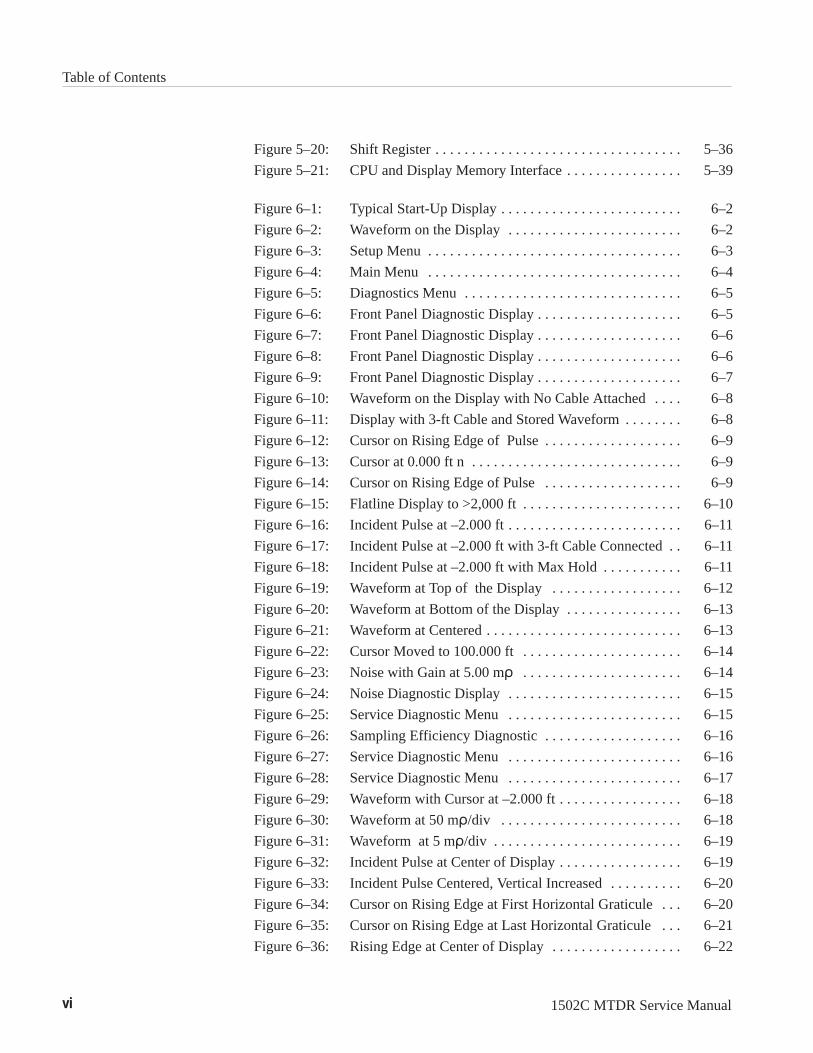
Table of Contents
vi 1502C MTDR Service Manual
Figure 5–20: Shift Register 5–36. . . . . . . . . . . . . . . . . . . . . . . . . . . . . . . . . .
Figure 5–21: CPU and Display Memory Interface 5–39. . . . . . . . . . . . . . . .
Figure 6–1: Typical Start-Up Display 6–2. . . . . . . . . . . . . . . . . . . . . . . . .
Figure 6–2: Waveform on the Display 6–2. . . . . . . . . . . . . . . . . . . . . . . .
Figure 6–3: Setup Menu 6–3. . . . . . . . . . . . . . . . . . . . . . . . . . . . . . . . . . .
Figure 6–4: Main Menu 6–4. . . . . . . . . . . . . . . . . . . . . . . . . . . . . . . . . . .
Figure 6–5: Diagnostics Menu 6–5. . . . . . . . . . . . . . . . . . . . . . . . . . . . . .
Figure 6–6: Front Panel Diagnostic Display 6–5. . . . . . . . . . . . . . . . . . . .
Figure 6–7: Front Panel Diagnostic Display 6–6. . . . . . . . . . . . . . . . . . . .
Figure 6–8: Front Panel Diagnostic Display 6–6. . . . . . . . . . . . . . . . . . . .
Figure 6–9: Front Panel Diagnostic Display 6–7. . . . . . . . . . . . . . . . . . . .
Figure 6–10: Waveform on the Display with No Cable Attached 6–8. . . .
Figure 6–11: Display with 3-ft Cable and Stored Waveform 6–8. . . . . . . .
Figure 6–12: Cursor on Rising Edge of Pulse 6–9. . . . . . . . . . . . . . . . . . .
Figure 6–13: Cursor at 0.000 ft n 6–9. . . . . . . . . . . . . . . . . . . . . . . . . . . . .
Figure 6–14: Cursor on Rising Edge of Pulse 6–9. . . . . . . . . . . . . . . . . . .
Figure 6–15: Flatline Display to >2,000 ft 6–10. . . . . . . . . . . . . . . . . . . . . .
Figure 6–16: Incident Pulse at –2.000 ft 6–11. . . . . . . . . . . . . . . . . . . . . . . .
Figure 6–17: Incident Pulse at –2.000 ft with 3-ft Cable Connected 6–11. .
Figure 6–18: Incident Pulse at –2.000 ft with Max Hold 6–11. . . . . . . . . . .
Figure 6–19: Waveform at Top of the Display 6–12. . . . . . . . . . . . . . . . . .
Figure 6–20: Waveform at Bottom of the Display 6–13. . . . . . . . . . . . . . . .
Figure 6–21: Waveform at Centered 6–13. . . . . . . . . . . . . . . . . . . . . . . . . . .
Figure 6–22: Cursor Moved to 100.000 ft 6–14. . . . . . . . . . . . . . . . . . . . . .
Figure 6–23: Noise with Gain at 5.00 m 6–14. . . . . . . . . . . . . . . . . . . . . .
Figure 6–24: Noise Diagnostic Display 6–15. . . . . . . . . . . . . . . . . . . . . . . .
Figure 6–25: Service Diagnostic Menu 6–15. . . . . . . . . . . . . . . . . . . . . . . .
Figure 6–26: Sampling Efficiency Diagnostic 6–16. . . . . . . . . . . . . . . . . . .
Figure 6–27: Service Diagnostic Menu 6–16. . . . . . . . . . . . . . . . . . . . . . . .
Figure 6–28: Service Diagnostic Menu 6–17. . . . . . . . . . . . . . . . . . . . . . . .
Figure 6–29: Waveform with Cursor at –2.000 ft 6–18. . . . . . . . . . . . . . . . .
Figure 6–30: Waveform at 50 m/div 6–18. . . . . . . . . . . . . . . . . . . . . . . . .
Figure 6–31: Waveform at 5 m/div 6–19. . . . . . . . . . . . . . . . . . . . . . . . . .
Figure 6–32: Incident Pulse at Center of Display 6–19. . . . . . . . . . . . . . . . .
Figure 6–33: Incident Pulse Centered, Vertical Increased 6–20. . . . . . . . . .
Figure 6–34: Cursor on Rising Edge at First Horizontal Graticule 6–20. . .
Figure 6–35: Cursor on Rising Edge at Last Horizontal Graticule 6–21. . .
Figure 6–36: Rising Edge at Center of Display 6–22. . . . . . . . . . . . . . . . . .

Table of Contents
1502C MTDR Service Manual vii
Figure 6–37: Rising Edge with Scale at 1.0 m/div 6–22. . . . . . . . . . . . . . .
Figure 6–38: Rising Edge with Max Hold on 6–22. . . . . . . . . . . . . . . . . . . .
Figure 6–39: Head Alignment Chart Print 6–23. . . . . . . . . . . . . . . . . . . . . .
Figure 6–40: Circuit Board Locations in the Instrument 6–25. . . . . . . . . . .
Figure 6–41: Power Supply Board 6–27. . . . . . . . . . . . . . . . . . . . . . . . . . . .
Figure 6–42: Power Supply Test Points TP1020 and TP1010 6–27. . . . . .
Figure 6–43: Power Supply Test Point TP2030 6–28. . . . . . . . . . . . . . . . .
Figure 6–44: Connector Plug P5040 and Pins J5040 on Bottom of Main Board 6–29. . . . . . . . . . . . . . . . . . . . . . . . . . . . . . . . . . .
Figure 6–45: Power Supply Test Point TP1020 6–29. . . . . . . . . . . . . . . . .
Figure 6–46: Power Supply Test Point TP2030 6–30. . . . . . . . . . . . . . . . .
Figure 6–47: Location of Main Board in Instrument 6–30. . . . . . . . . . . . . .
Figure 6–48: Main Board Probe Points 6–31. . . . . . . . . . . . . . . . . . . . . . . .
Figure 6–49: Waveform on Display 6–31. . . . . . . . . . . . . . . . . . . . . . . . . . .
Figure 6–50: Battery Connections to Power Supply Board 6–32. . . . . . . . .
Figure 6–51: CR2012 on Power Supply Board 6–33. . . . . . . . . . . . . . . . . .
Figure 6–52: Display Showing Power is Battery 6–33. . . . . . . . . . . . . . . . .
Figure 6–53: Display Showing Battery Voltage is Low 6–33. . . . . . . . . . . .
Figure 6–54: R2012 on Power Supply Board 6–34. . . . . . . . . . . . . . . . . . . .
Figure 6–55: Driver/Sampler Board Location 6–35. . . . . . . . . . . . . . . . . . .
Figure 6–56: TP1030 on Driver/Sampler Board 6–35. . . . . . . . . . . . . . . . .
Figure 6–57: R1018 on Front Panel Board 6–36. . . . . . . . . . . . . . . . . . . . . .
Figure 6–58: LCD Pattern with Contrast Too Light 6–36. . . . . . . . . . . . . . .
Figure 6–59: LCD Pattern with Contrast Too Dark 6–37. . . . . . . . . . . . . . .
Figure 6–60: LCD Pattern Adjusted for Sharpness 6–37. . . . . . . . . . . . . . .
Figure 6–61: Waveform with Contrast Too Light 6–38. . . . . . . . . . . . . . . . .
Figure 6–62: Waveform with Contrast Adjusted Correctly 6–38. . . . . . . . .
Figure 6–63: Driver/Sampler Board Location 6–39. . . . . . . . . . . . . . . . . . .
Figure 6–64: Incident Pulse at –2.000 ft 6–40. . . . . . . . . . . . . . . . . . . . . . . .
Figure 6–65: R1042 on Driver/Sampler Board 6–40. . . . . . . . . . . . . . . . . .
Figure 7–1: Location of Voltage Selector and Fuse Holder onRear Panel 7–2. . . . . . . . . . . . . . . . . . . . . . . . . . . . . . . . . . . .
Figure 7–2: Power Supply Module and P/O Rear Panel 7–4. . . . . . . . . .
Figure 7–3: Main Board 7–7. . . . . . . . . . . . . . . . . . . . . . . . . . . . . . . . . . .
Figure 7–4: EPROM on Main Board 7–7. . . . . . . . . . . . . . . . . . . . . . . . .
Figure 7–5: Lithium Battery on Main Board 7–8. . . . . . . . . . . . . . . . . . .
Figure 7–6: Display Module/Front Panel Board Screw Locations 7–10. . .
Figure 7–7: Display Module/Front Panel Board Showing Hex Nuts 7–10.

Table of Contents
viii 1502C MTDR Service Manual
Figure 7–8: Location of Default Jumper on Front Panel Board 7–11. . . . .
Figure 7–9: Default Jumper Positions 7–11. . . . . . . . . . . . . . . . . . . . . . . .
Figure 7–10: Main Board TP1041 and TP3040 7–16. . . . . . . . . . . . . . . . . .
Figure 7–11: Main Board TP3041 and TP4040 7–16. . . . . . . . . . . . . . . . . .
Figure 7–12: Main Board TP6010 and TP7010 7–16. . . . . . . . . . . . . . . . . .
Figure 7–13: Main Board TP9011 and TP9041 7–17. . . . . . . . . . . . . . . . . .
Figure 7–14: Front Panel CABLE Connector 7–17. . . . . . . . . . . . . . . . . . .
Figure 7–15: Installing the Case Cover Over the Chassis 7–19. . . . . . . . . .
Figure 9–1: Special Schematic Symbols 9–3. . . . . . . . . . . . . . . . . . . . . .
Figure 9–2: Component Locator – Main Board 9–13. . . . . . . . . . . . . . . . .
Schematics – Main Board 9–14. . . . . . . . . . . . . . . . . . . . . . . .
Figure 9–3: Component Locator – Front Panel Board 9–23. . . . . . . . . . . .
Schematics – Front Panel 9–24. . . . . . . . . . . . . . . . . . . . . . . .
Figure 9–4: Component Locator – Power Supply Board 9–26. . . . . . . . . .
Schematics – Power Supply 9–27. . . . . . . . . . . . . . . . . . . . . .
Figure 9–5: Component Locator – Driver/Sampler Board 9–29. . . . . . . . .
Schematics – Driver/Sampler 9–30. . . . . . . . . . . . . . . . . . . . .
Figure 10–1: Cabinet 10–13. . . . . . . . . . . . . . . . . . . . . . . . . . . . . . . . . . . . . .
Figure 10–2: Frame, Assemblies and Front Panel Controls 10–15. . . . . . . . .
Figure 10–3: Power Supply 10–17. . . . . . . . . . . . . . . . . . . . . . . . . . . . . . . . .

Table of Contents
1502C MTDR Service Manual ix
List of Tables
Shipping Carton Test Strength xv. . . . . . . . . . . . . . . . . . . . . . . . . . . . . . . . . .
Fuse / Voltage Ratings 1–2. . . . . . . . . . . . . . . . . . . . . . . . . . . . . . . . . . . . . . . .
Vp of Various Dielectric Types 1–11. . . . . . . . . . . . . . . . . . . . . . . . . . . . . . . . .
Operator Performance Checks – Equipment Required 2–1. . . . . . . . . . . . . . .
Specifications: Electrical Characteristics 3–1. . . . . . . . . . . . . . . . . . . . . . . . .
Specifications: Environmental Characteristics 3–3. . . . . . . . . . . . . . . . . . . . .
Certifications and Compliances 3–4. . . . . . . . . . . . . . . . . . . . . . . . . . . . . . . . .
Specifications: Physical Characteristics 3–5. . . . . . . . . . . . . . . . . . . . . . . . . .
Option Port Wiring Configuration 5–12. . . . . . . . . . . . . . . . . . . . . . . . . . . . . . .
Row Driver Latch Bits 5–34. . . . . . . . . . . . . . . . . . . . . . . . . . . . . . . . . . . . . . . .
Column Driver Latch Bits 5–36. . . . . . . . . . . . . . . . . . . . . . . . . . . . . . . . . . . . .
Controller Periods 5–37. . . . . . . . . . . . . . . . . . . . . . . . . . . . . . . . . . . . . . . . . . .
Calibration Performance Check – Equipment Required 6–1. . . . . . . . . . . . . .
Adjustment Procedures – Equipment Required 6–25. . . . . . . . . . . . . . . . . . . .
Main Board Voltages, Tolerances, Test Point Locations 6–28. . . . . . . . . . . . . .
Maintenance – Equipment Required 7–1. . . . . . . . . . . . . . . . . . . . . . . . . . . . .
Power Cord Conductor Color Code 7–6. . . . . . . . . . . . . . . . . . . . . . . . . . . . .
Sealing Materials 7–18. . . . . . . . . . . . . . . . . . . . . . . . . . . . . . . . . . . . . . . . . . . .

Table of Contents
x 1502C MTDR Service Manual

1502C MTDR Service Manual xi
General Safety Summary
Review the following safety precautions to avoid injury and prevent damage tothis product or any products connected to it. To avoid potential hazards, use thisproduct only as specified.
Only qualified personnel should perform service procedures.
Use Proper Power Cord. Use only the power cord specified for this product andcertified for the country of use.
Use Proper Voltage Setting. Before applying power, ensure that the line selector isin the proper position for the power source being used.
This product is intended to operate from a power source that will not apply more than250 volts RMS between the supply conductors or between the supply conductor andground. A protective ground connection, by way of the grounding conductor in thepower cord, is essential for safe operation.
Ground the Product. This product is grounded through the grounding conductorof the power cord. To avoid electric shock, the grounding conductor must beconnected to earth ground. Before making connections to the input or outputterminals of the product, ensure that the product is properly grounded.
The standard power cord (161–0288–00) is rated for outdoor use. All other optionalpower cords are rated for indoor use only.
Observe All Terminal Ratings. To avoid fire or shock hazard, observe all ratingsand markings on the product. Consult the product manual for further ratingsinformation before making connections to the product.
Do not apply a potential to any terminal, including the common terminal, thatexceeds the maximum rating of that terminal.
Replace Batteries Properly. Replace batteries only with the proper type and ratingspecified.
Recharge Batteries Properly. Recharge batteries for the recommended chargecycle only.
Use Proper AC Adapter. Use only the AC adapter specified for this product.
Do Not Operate Without Covers. Do not operate this product with covers or panelsremoved.
Use Proper Fuse. Use only the fuse type and rating specified for this product.
Avoid Exposed Circuitry. Do not touch exposed connections and componentswhen power is present.
To Avoid Fire or Personal Injury
Power Source

General Safety Summary
xii 1502C MTDR Service Manual
Do Not Operate With Suspected Failures. If you suspect there is damage to thisproduct, have it inspected by qualified service personnel.
Do Not Operate in an Explosive Atmosphere.
Terms in this Manual. These terms may appear in this manual:
WARNING. Warning statements identify conditions or practices that could resultin injury or loss of life.
CAUTION. Caution statements identify conditions or practices that could result indamage to this product or other property.
Terms on the Product. These terms may appear on the product:
DANGER indicates an injury hazard immediately accessible as you read themarking.
WARNING indicates an injury hazard not immediately accessible as you read themarking.
CAUTION indicates a hazard to property including the product.
Symbols on the Product. The following symbols may appear on the product:
CAUTIONRefer to Manual
WARNINGHigh Voltage
DoubleInsulated
Protective Ground(Earth) Terminal
Symbols and Terms

1502C MTDR Service Manual xiii
Service Safety Summary
Only qualified personnel should perform service procedures. Read this ServiceSafety Summary and the General Safety Summary before performing any serviceprocedures.
Do not perform internal service or adjustments of this product unless another personcapable of rendering first aid and resuscitation is present.
To avoid electric shock, disconnect the main power by means of the power cord orthe power switch.
Dangerous voltages or currents may exist in this product. Disconnect power, removebattery, and disconnect test leads before removing protective panels, soldering, orreplacing components.
To avoid electric shock, do not touch exposed connections.
This instrument contains a lead-acid battery. Some states and/or local jurisdictionsmight require special disposition/recycling of this type of material in accordancewith Hazardous Waste guidelines. Check your local and state regulations prior todisposing of an old battery.
Tektronix Factory Service will accept 1502C batteries for recycling. If you chooseto return the battery to us for recycling, the battery cases must be intact, the batteryshould be packed with the battery terminals insulated against possible short-circuits,and should be packed in shock-absorbant material.
Tektronix, Inc.Attn: Service DepartmentP.O. Box 500Beaverton, Oregon 97077 U.S.A.
For additional information, phone:1-800-TEK-WIDE
Do Not Service Alone
Disconnect Power
Use Care When ServicingWith Power On
Disposal of Batteries

Service Safety Summary
xiv 1502C MTDR Service Manual
1502C MTDR Service Manual xv
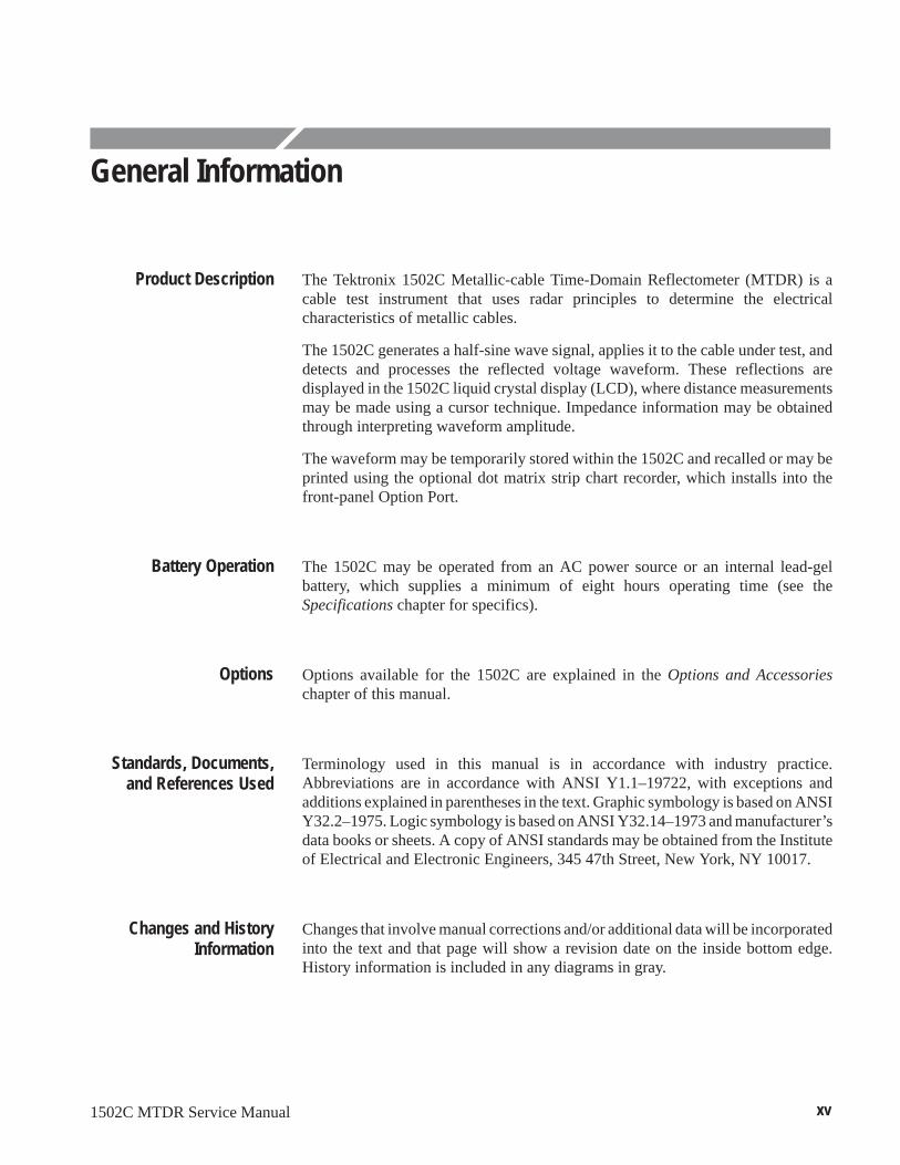
General Information
The Tektronix 1502C Metallic-cable Time-Domain Reflectometer (MTDR) is acable test instrument that uses radar principles to determine the electricalcharacteristics of metallic cables.
The 1502C generates a half-sine wave signal, applies it to the cable under test, anddetects and processes the reflected voltage waveform. These reflections aredisplayed in the 1502C liquid crystal display (LCD), where distance measurementsmay be made using a cursor technique. Impedance information may be obtainedthrough interpreting waveform amplitude.
The waveform may be temporarily stored within the 1502C and recalled or may beprinted using the optional dot matrix strip chart recorder, which installs into thefront-panel Option Port.
The 1502C may be operated from an AC power source or an internal lead-gelbattery, which supplies a minimum of eight hours operating time (see theSpecifications chapter for specifics).
Options available for the 1502C are explained in the Options and Accessorieschapter of this manual.
Terminology used in this manual is in accordance with industry practice.Abbreviations are in accordance with ANSI Y1.1–19722, with exceptions andadditions explained in parentheses in the text. Graphic symbology is based on ANSIY32.2–1975. Logic symbology is based on ANSI Y32.14–1973 and manufacturer’sdata books or sheets. A copy of ANSI standards may be obtained from the Instituteof Electrical and Electronic Engineers, 345 47th Street, New York, NY 10017.
Changes that involve manual corrections and/or additional data will be incorporatedinto the text and that page will show a revision date on the inside bottom edge.History information is included in any diagrams in gray.
Product Description
Battery Operation
Options
Standards, Documents,and References Used
Changes and HistoryInformation

General Information
xvi 1502C MTDR Service Manual
Installation and Repacking
Before unpacking the 1502C from its shipping container or carton, inspect for signsof external damage. If the carton is damaged, notify the carrier. The shipping cartoncontains the basic instrument and its standard accessories. Refer to the replaceableparts list in the Service Manual for a complete listing.
If the contents of the shipping container are incomplete, if there is mechanicaldamage or defect, or if the instrument does not meet operational check requirements,contact your local Tektronix Field Office or representative. If the shipping containeris damaged, notify the carrier as well as Tektronix.
The instrument was inspected both mechanically and electrically before shipment.It should be free if mechanical damage and meet or exceed all electricalspecifications. Procedures to check operational performance are in the PerformanceChecks appendix. These checks should satisfy the requirements for most receivingor incoming inspections.
The 1502C is intended to be operated from a power source that will not apply morethan 250 volts RMS between the supply conductors or between either supplyconductor and ground. A protective ground connection, by way of the groundingconductor in the power cord, is essential for safe operation.
The AC power connector is a three-way polarized plug with the ground (earth) leadconnected directly to the instrument frame to provide electrical shock protection. Ifthe unit is connected to any other power source, the unit frame must be connectedto earth ground.
Power and voltage requirements are printed on the back panel. The 1502C can beoperated from either 115 VAC or 230 VAC nominal line voltage at 45 Hz to 440 Hz,or a 12 VDC supply, or an internal battery.
Further information on the 1502C power requirements can be found in the SafetySummary in this section and in the Operating Instructions chapter.
When the 1502C is to be shipped to a Tektronix Service Center for service or repair,attach a tag showing the name and address of the owner, name of the individual atyour firm who may be contacted, the complete serial number of the instrument, anda description of the service required. If the original packaging is unfit for use or isnot available, repackage the instrument as follows:
1. Obtain a carton of corrugated cardboard having inside dimensions that are atleast six inches greater than the equipment dimensions to allow for cushioning.The test strength of the shipping carton should be 275 pounds (102.5 kg). Referto the following table for test strength requirements:
Unpacking and InItialInspection
Power Source and PowerRequirements
Repacking for Shipment

General Information
1502C MTDR Service Manual xvii
SHIPPING CARTON TEST STRENGTH
Gross Weight (lb) Carton Test Strength (lb)
0 – 10 200
11 – 30 275
31 – 120 375
121 – 140 500
141 – 160 600
CAUTION. The battery pack should be removed from the instrument before shipping.If it is necessary to ship the battery, it should be wrapped and secured separatelybefore being packed with the instrument.
2. Install the front cover on the 1502C and surround the instrument withpolyethylene sheeting to protect the finish.
3. Cushion the instrument on all sides with packing material or urethane foambetween the carton and the sides of the instrument.
4. Seal with shipping tape or an industrial stapler.
If you have any questions, contact your local Tektronix Field Office orrepresentative.

General Information
xviii 1502C MTDR Service Manual
Contacting Tektronix
ProductSupport
For questions about using Tektronix measurement products, calltoll free in North America:1-800-833-92006:00 a.m. – 5:00 p.m. Pacific time
Or contact us by e-mail:[email protected]
For product support outside of North America, contact your localTektronix distributor or sales office.
Servicesupport
Tektronix offers a range of services, including Extended WarrantyRepair and Calibration services. Contact your local Tektronixdistributor or sales office for details.
For a listing of worldwide service centers, visit our web site.
Toll-freeNumber
In North America:1-800-833-9200An operator can direct your call.
Postal Address
Tektronix, Inc.Department or name (if known)P.O. Box 500Beaverton, OR 97077USA
Web site www.tektronix.com

1502C MTDR Service Manual 1–1
Operating Instructions
Overview
The 1502C front panel is protected by a watertight cover, in which the standardaccessories are stored. Secure the front cover by snapping the side latches outward.If the instrument is inadvertently left on, installing the front cover will turn off thePOWER switch automatically.
The carrying handle rotates 325° and serves as a stand when positioned beneath theinstrument.
Inside the case, at the back of the instrument, is a moisture-absorbing canistercontaining silica gel. In extremely wet environments, it might be be necessary toperiodically remove and dry the canister. This procedure is explained in the 1502CService Manual.
The 1502C can be stored in temperatures ranging from –62° C to +85° C. However,if the temperature is below –40° C or above +55° C, the battery pack should beremoved and stored separately. Battery storage temperature should be –40° C to+55° C.
In the field, the 1502C can be powered using the internal battery. For AC operation,check the rear panel for proper voltage setting. The voltage selector can be seenthrough the window of the protective cap. If the setting differs from the voltageavailable, it can be easily changed. Simply remove the protective cap and select theproper voltage using a screwdriver.
REMOVECAP TOREPLACE
FUSE
REMOVECAP TOSELECTVOLTAGE
VoltageSelector
Line Fuse
AC PowerCord Receptacle
Figure 1–1: Rear Panel Voltage Selector, Fuse, AC Receptacle
Handling
Powering the 1502C
Operating Instructions
1–2 1502C MTDR Service Manual
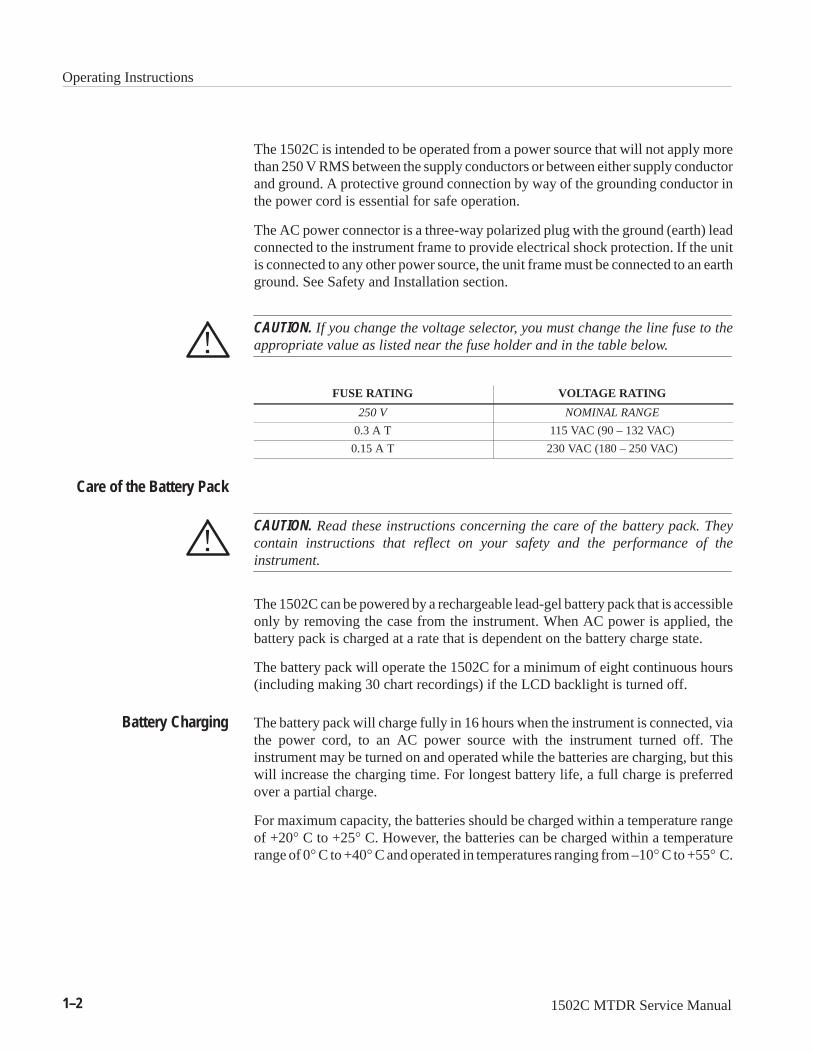
The 1502C is intended to be operated from a power source that will not apply morethan 250 V RMS between the supply conductors or between either supply conductorand ground. A protective ground connection by way of the grounding conductor inthe power cord is essential for safe operation.
The AC power connector is a three-way polarized plug with the ground (earth) leadconnected to the instrument frame to provide electrical shock protection. If the unitis connected to any other power source, the unit frame must be connected to an earthground. See Safety and Installation section.
CAUTION. If you change the voltage selector, you must change the line fuse to theappropriate value as listed near the fuse holder and in the table below.
FUSE RATING VOLTAGE RATING
250 V NOMINAL RANGE
0.3 A T 115 VAC (90 – 132 VAC)
0.15 A T 230 VAC (180 – 250 VAC)
CAUTION. Read these instructions concerning the care of the battery pack. Theycontain instructions that reflect on your safety and the performance of theinstrument.
The 1502C can be powered by a rechargeable lead-gel battery pack that is accessibleonly by removing the case from the instrument. When AC power is applied, thebattery pack is charged at a rate that is dependent on the battery charge state.
The battery pack will operate the 1502C for a minimum of eight continuous hours(including making 30 chart recordings) if the LCD backlight is turned off.
The battery pack will charge fully in 16 hours when the instrument is connected, viathe power cord, to an AC power source with the instrument turned off. Theinstrument may be turned on and operated while the batteries are charging, but thiswill increase the charging time. For longest battery life, a full charge is preferredover a partial charge.
For maximum capacity, the batteries should be charged within a temperature rangeof +20° C to +25° C. However, the batteries can be charged within a temperaturerange of 0° C to +40° C and operated in temperatures ranging from –10° C to +55° C.
Care of the Battery Pack
Battery Charging

Operating Instructions
1502C MTDR Service Manual 1–3
CAUTION. Do not charge battery pack below 0° C or above +40° C. Do notdischarge battery pack below –10° C or above +55° C. If removing the battery packduring or after exposure to these extreme conditions, turn the instrument off andremove the AC power cord.
The battery pack should be stored within a temperature range of –35° C to +65° C.However, the self-discharge rate will increase as the temperature increases.
If the instrument is stored with the battery pack installed, the battery pack shouldbe charged every 90 days. A fully charged battery pack will lose about 12% of itscapacity in three to four months if stored between +20° C and +25° C.
NOTE. The battery pack in the 1502C is inside the instrument case with no externalaccess. Refer removal and replacement to qualified service personnel.
1. Ensure that the instrument power is off.
2. If the instrument is connected to an AC power source, remove the AC powercable from the source and from the instrument.
3. If installed, remove the chart recorder, or other device, from the option port.
4. Loosen the four screws on the back of the case and set the instrument face-upon a flat surface.
5. Swing the handle out of the way of the front panel.
6. Break the chassis seal by pushing downward with both hands on the handlepivots on each side of the case.
7. Grasp the case with one hand and tilt the chassis out with the other. Lift bygrasping the outside perimeter of the front panel.
CAUTION. Do not lift the instrument by the front-panel controls. The controls willbe damaged if you do so.
8. Remove the top shield from the instrument by gently lifting the rear edge nearthe sides of the instrument.
9. Unplug the battery cable positive lead at the battery.
10. Unplug the battery cable negative lead at the battery.
11. Unplug the battery cable at the power supply.
12. Remove the cable.
Battery Removal

Operating Instructions
1–4 1502C MTDR Service Manual
13. Remove the two screws mounting the battery clamp to the chassis.
14. Carefully remove the clamp without touching the battery terminals.
15. Lift the battery out.
To re-install or replace the battery, repeat the above steps in reverse order.
If the battery is low, it will be indicated on the LCD (bat/low). If this is the case,protective circuitry will shut down the 1502C within minutes. Either switch to ACpower or work very fast. If the instrument is equipped with a chart recorder, usingthe recorder will further reduce the battery level, or the added load might shut downthe instrument.
OFF
OFF
OFF
ON
1 avg 500 m 500 ft
bat/low 0.000 ft
Low BatteryIndicator
Figure 1–2: Display Showing Low Battery Indication
Protection circuits in the charger prevent deep discharge of the batteries duringinstrument operation. The circuits automatically shut down the instrumentwhenever battery voltage falls below approximately 10 V. If shutdown occurs, thebatteries should be fully recharged before further use.
NOTE. Turn the POWER switch off after instrument shutdown to prevent continueddischarge of the batteries.
Under low AC voltage conditions, AC fuse ratings might be exceeded if the batteryif fully discharged and a chart recording is being made. Allow the battery to chargefor about one hour before attempting to make a chart recording, or use AC only.
When operating the 1502C in an environment below +10° C, a heater will activate.The element is built into the LCD module and will heat the display to permit normaloperation. Depending on the surrounding temperature, it might take up to 15minutes to completely warm the crystals in the LCD. Once warmed, the display willoperate normally.
Low Battery
Low TemperatureOperation

Operating Instructions
1502C MTDR Service Manual 1–5
Preparing to Use the 1502CCheck the power requirements, remove the front cover, and you are ready to testcables. The following pages explain the front-panel controls.
OFF
OFF
OFF
ON
1 avg 500 m
ac 0.00 ftMENU
VIEWINPUT
VIEWSTORE
VIEWDIFF
STORE
POSITION
DO NOT APPLY
POWER(PULL ON)
POSITION
NOISE FILTER VERT SCALE DIST/DIV
SET REFHORZ
VERT
.3.4 .5
.6.7.8
.9 .00.01.02.03
.04 .05.06.07
.08.09
Vp
METALLIC TDRCABLE TESTER1502BTektronix
1 3 4 5 6
7
9
10
11
12
13
0.2 ft
2
8
EXT VOLTAGE
Figure 1–3: 1502C Front-Panel Controls
CAUTION. Do not connect live circuits to the CABLE connector. Voltages exceeding5 volts can damage the driver or sampler circuits.
Bleed the test cable of any residual static charge before attaching it to theinstrument. To bleed the cable, connect the standard 50 terminator and standardfemale-to-female BNC connector together, then temporarily attach both to thecable. Remove the connectors before attaching the cable to the instrument.
When testing receiving antenna cables, avoid close proximity to transmitters.Voltages may appear on the cable if a nearby transmitter is in use, resulting indamage to the instrument. Before testing, be sure that there are no RF voltagespresent, or disconnect the cable at both ends.

Operating Instructions
1–6 1502C MTDR Service Manual
Display
OFF
OFF
OFF
ON
1 avg 500 m 0.2 ft
ac 0.000 ft
PowerType CursorWaveform
Front-Panel to CursorDistance Window
Grid
SelectedNoise Filter
Selected SelectedVertical Scale Distance per
Division
View InputIndicator
View Store
View Difference
Store
Indicator
Indicator
Indicator
Figure 1–4: Display and Indicators
Front-Panel Controls1. CABLE: A female BNC connector for attaching a cable to the 1502C for
testing.
2. NOISE FILTER: If the displayed waveform is noisy, the apparent noise canbe reduced by using noise averaging. Averaging settings are between 1 and 128.The time for averaging is directly proportional to the averaging setting chosen.A setting of 128 might take the instrument up to 35 seconds to acquire anddisplay a waveform. The first two positions on the NOISE FILTER control areused for setting the vertical and horizontal reference points. The selected valueor function is displayed above the control on the LCD.
3. VERT SCALE: This control sets the vertical sensitivity, displayed in m perdivision, or the vertical gain, displayed in dB. Although the instrument defaultsto millirho, you may choose the preferred mode from the Setup Menu. Theselected value is displayed above the control on the LCD.
4. DIST/DIV: Determines the number of feet (or meters) per division across thedisplay. The minimum setting is 0.1 ft/div (0.025 meters) and the maximumsetting is 200 ft/div (50 meters). The selected value is displayed above thecontrol on the LCD.
A standard instrument defaults to ft/div. A metric instrument (Option 05)defaults to m/div, but either may be changed temporarily from the menu. Thedefault can be changed by changing an internal jumper (see 1502C ServiceManual and always refer such changes to qualified service personnel).
NOISE FILTER
VERT SCALE
DIST/DIV

Operating Instructions
1502C MTDR Service Manual 1–7
5. Vp: The two Velocity of Propagation controls are set according to thepropagation velocity factor of the cable being tested. For example, solidpolyethylene commonly has a Vp of 0.66. Solid polytetraflourethylene (Teflon) is approximately 0.70. Air is 0.99. The controls are decaded: the left controlis the first digit and the right control is the second digit. For example, with a Vpof 0.30, the first knob would be set to .3 and the second knob to .00.
6. POWER: Pull for power ON and push in for power OFF. When the front coveris installed, this switch is automatically pushed OFF.
7.
POSITION: This is a continuously rotating control that positions thedisplayed waveform vertically, up or down the LCD.
8.
POSITION: This is a continuously rotating control that moves a verticalcursor completely across the LCD graticule. In addition, the waveform is alsomoved when the cursor reaches the extreme right or left side of the display. Areadout (seven digits maximum) is displayed in the upper right corner of theLCD, showing the distance from the front panel BNC to the current cursorlocation.
9. MENU: This pushbutton provides access to the menus and selects items chosenfrom the menus.
10. VIEW INPUT: When pushed momentarily, this button toggles the display ofthe waveform acquired at the CABLE connector. This function is useful to stopdisplaying a current waveform to avoid confusion when looking at a storedwaveform. This function defaults to ON when the instrument is powered up.
11. VIEW STORE: When pushed momentarily, this button toggles the display ofthe stored waveform.
12. VIEW DIFF: When pushed momentarily, this button toggles the display of thecurrent waveform minus the stored waveform and shows the difference betweenthem.
13. STORE: When pushed momentarily, the waveform currently displayed will bestored in the instrument memory. If a waveform is already stored, pushing thisbutton will erase it. The settings of the stored waveform are available from thefirst level menu under View Stored Waveform Settings.
Menu SelectionsThere are several layers of menu, as explained below.
The Main Menu is entered by pushing the MENU button on the front panel.
1. Return to Normal Operations puts the instrument into normal operationmode.
Vp
.3.4 .5
.6
.7
.8
.9 .00
.01
.02
.03.04 .05
.06
.07
.08
.09
POWER(PULL ON)
POSITION
POSITION
MENU
VIEWINPUT
VIEWSTORE
VIEWDIFF
STORE
Main Menu

Operating Instructions
1–8 1502C MTDR Service Manual
2. Help with Instrument Controls explains the operation of each control. Whena control or switch is adjusted or pushed, a brief explanation appears on theLCD.
3. Cable Information has these choices:
a. Help with Cables gives a brief explanation of cable parameters.
b. Velocity of Propagation Values displays a table of common dielectrics andtheir Vp values. These are nominal values. The manufacturer’s listedspecifications should be used whenever possible.
c. Impedance Values displays impedances of common cables. In some cases,these values have been rounded off. Manufacturer’s specifications shouldbe checked for precise values.
d. Finding Unknown Vp Values describes a procedure for finding anunknown Vp.
4. Setup Menu controls the manner in which the instrument obtains and displaysits test results.
a. Acquisition Control Menu has these choices:
i. Max Hold Is: On/Off. Turn Max Hold on by pushing MENU thenSTORE. In this mode, waveforms are accumulated on the display. MaxHold can be deactivated by pushing STORE or the mode exited byusing the Setup Menu.
ii. Pulse Is: On/Off. Turns the pulse generator off so the 1502C does notsend out pulses.
iii. Single Sweep Is: On/Off. This function is much like a still camera; itwill acquire one waveform and hold it.
b. Ohms-at-Cursor is: On/Off. When activated, the impedance at thee pointof the cursor is displayed beneath the distance window on the display.
c. Vertical Scale Is: dB/m. This offers you a choice as to how the verticalgain of the instrument is displayed. You may choose decibels or millirho.When powered down, the instrument will default to millirho when poweredback up.
d. Distance/Div Is: ft/m. Offers you a choice of how the horizontal scale isdisplayed. You may choose from feet per division or meters per division.When powered up, the instrument will default to feet unless the internaljumper has been moved to the meters position. Instructions on changing thisdefault are contained in the 1502C Service Manual.
e. Light Is: On/Off. This control turns the electroluminescent backlightbehind the LCD on or off.

Operating Instructions
1502C MTDR Service Manual 1–9
5. Diagnostics Menu lists an extensive selection of diagnostics to test theoperation of the instrument.
NOTE. The Diagnostics Menu is intended for instrument repair and calibration.Proper instrument setup is important for correct diagnostics results. Refer to the1502C Service Manual for more information on diagnostics.
a. Service Diagnostics Menu has these choices:
i. Sampling Efficiency Diagnostic displays a continuous efficiencydiagnostic of the sampling circuits.
ii. Noise Diagnostic measures the internal RMS noise levels of theinstrument.
iii. Offset/Gain Diagnostic reports out-of-tolerance steps in the program-mable gain stage. This can help a service technician to quickly isolatethe cause of waveform distortion problems.
iv. RAM/ROM Diagnostics Menu performs tests on the RAM (RandomAccess Memory) and the ROM (Read Only Memory).
v. Timebase Is: Normal - Auto Correction / Diagnostic - NoCorrection. When in Normal - Auto Correction, the instrumentcompensates for variations in temperature and voltage. This conditionmight not be desirable while calibrating the instrument. While inDiagnostic - No Correction, the circuits will not correct for thesevariations.
b. Front Panel Diagnostics aids in testing the front panel.
c. LCD Diagnostics Menu has these choices:
i. LCD Alignment Diagnostic generates a dot pattern of every otherpixel on the LCD. These pixels can be alternated to test the LCD.
ii. Response Time Diagnostic generates alternate squares of dark andlight, reversing their order. This tests the response time of the LCD andcan give an indication of the effectiveness of the LCD heater in a coldenvironment.
iii. LCD Drive Test Diagnostic generates a moving vertical bar patternacross the LCD.
iv. Contrast Adjust allows you to adjust the contrast of the LCD. Itgenerates an alternating four-pixel pattern. The nominal contrast is setinternally. When in Contrast Adjust mode, VERT SCALE is used as thecontrast adjustment control. This value ranges from 0 to 255 units and

Operating Instructions
1–10 1502C MTDR Service Manual
is used by the processor to evaluate and correct circuit variations causedby temperature changes in the environment. When the diagnostic menuis exited, the LCD contrast returns to that set by internal adjust.
d. Chart Diagnostics Menu offers various tests for the optional chartrecorder.
i. LCD Chart allows adjusting the number of dots per segment and thenumber of prints (strikes) per segment.
ii. Head Alignment Chart generates a pattern to allow mechanicalalignment of the optional chart recorder.
6. View Stored Waveform Settings displays the instrument settings for the storedwaveform.
7. Option Port Menu contains three items. Two items allow configuration of theoption port for communicating with devices other than the optional chartrecorder and one item test the option port.
a. Option Port Diagnostic creates a repeating pattern of signals at the optionport to allow service technicians to verify that all signals are present andworking correctly.
b. Set Option Port Timing allows adjustment of the data rate used tocommunicate with external devices. The timing rate between bytes can beset from about 0.05 to 12.8 milliseconds.
c. Option Port Debugging Is Off/On. Off is quiet, On is verbose. Thischooses how detailed the error message reporting will be when communi-cating with an external device.
It is possible to connect the instrument to a computer through a parallel interfacewith a unique software driver. Because different computers vary widely inprocessing speed, the instrument must be able to adapt to differing data rateswhile communicating with those computers. With user-developed softwaredrivers, the ability to obtain detailed error messages during the development canbe very useful. For more information, contact your Tektronix Customer Servicerepresentatives. They have information describing the option port hardware andsoftware protocol and custom development methods available.
8. Display Contrast (Software Version 5.02 and above)
a. Press the MENU button firmly once. If the display is very light or very dark,you might not be able to see a change in the contrast.
b. Turn the VERTICAL SCALE knob slowly clockwise to darken the displayor counterclockwise to lighten the display. If you turn the knob far enough,the contrast will wrap from the darkest to lightest value.

Operating Instructions
1502C MTDR Service Manual 1–11
c. When the screen is clearly readable, press the MENU button again to returnto normal measurement operation. The new contrast value will remain ineffect until the instrument is turned off.
Test PreparationsVp is the speed of a signal down the cable given as a percentage of the speed of lightin free space. It is sometimes expressed as a whole number (e.g., 66) or a percentage(e.g., 66%). On the 1502C, it is the percentage expressed as a decimal number (e.g.,66% = .66). If you do not know the velocity of propagation, you can get a generalidea from the following table, or use the Help with Cables section of the CableInformation menu. You can also find the Vp with the procedure that follows usinga cable sample.
NOTE. If you do not know the Vp of your cable, it will not prevent you from findinga fault in your cable. However, if the Vp is set wrong, the distance readings will beaffected.
All Vp settings should be set for the cable under test, not the supplied jumper cable.
Dielectric Probable Vp
Jelly Filled .64
Polyethylene (PIC, PE, or SPE) .66
PTFE (Teflon ) or TFE .70
Pulp Insulation .72
Foam or Cellular PE (FPE) .78
Semi-solid PE (SSPE) .84
Air (helical spacers) .98
1. Obtain a known length of cable of the exact type you wish to test. Attach thecable to the CABLE connector on the front panel.
2. Pull POWER on.
3. Turn the DIST/DIV to an appropriate setting (e.g., if trying to find the Vp of athree-foot cable, turn the DIST/DIV to 1 ft/div).
4. Turn the
POSITION control until the distance reading is the same as theknown length of this cable.
The Importance of Vp(Velocity of Propagation)
Vp of Various DielectricTypes
Finding an Unknown Vp
Operating Instructions
1–12 1502C MTDR Service Manual
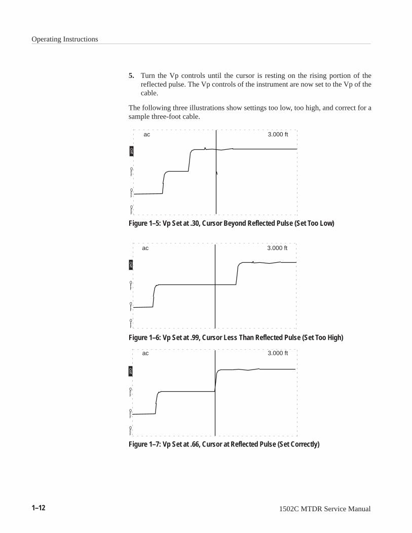
5. Turn the Vp controls until the cursor is resting on the rising portion of thereflected pulse. The Vp controls of the instrument are now set to the Vp of thecable.
The following three illustrations show settings too low, too high, and correct for asample three-foot cable.
OFF
OFF
OFF
ON
ac 3.000 ft
Figure 1–5: Vp Set at .30, Cursor Beyond Reflected Pulse (Set Too Low)
OFF
OFF
OFF
ON
ac 3.000 ft
Figure 1–6: Vp Set at .99, Cursor Less Than Reflected Pulse (Set Too High)
OFF
OFF
OFF
ON
ac 3.000 ft
Figure 1–7: Vp Set at .66, Cursor at Reflected Pulse (Set Correctly)

Operating Instructions
1502C MTDR Service Manual 1–13
Cable Test ProcedureBe sure to read the previous paragraphs on Vp.
1. Set the 1502C controls:
POWER OnCABLE Cable to BNCNOISE FILTER 1 avgVERT SCALE 500 m
DIST/DIV (see below)Vp (per cable)
2. If you know approximately how long the cable is, set the DIST/DIVappropriately (e.g., 20-ft cable would occupy four divisions on the LCD if 5ft/div was used). The entire cable should be displayed.
OFF
OFF
OFF
ON
ac 0.000 ft
Figure 1–8: 20-ft Cable at 5 ft/div
If the cable length is unknown, set DIST/DIV to 200 ft/div and continue to decreasethe setting until the reflected pulse is visible. Depending on the cable length and theamount of pulse energy absorbed by the cable, it might be necessary to increase theVERT SCALE to provide more gain to see the reflected pulse.
OFF
OFF
OFF
ON
ac 20.000 ft
Short
Figure 1–9: Short in the Cable
Distance to the Fault
Operating Instructions
1–14 1502C MTDR Service Manual
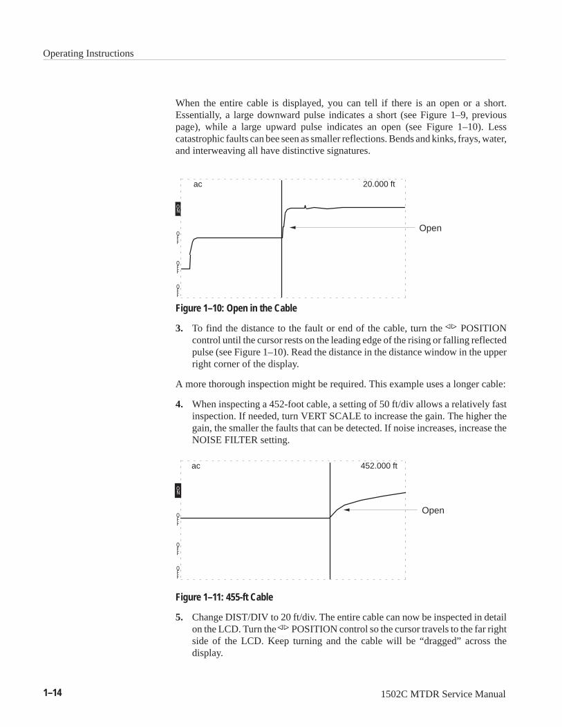
When the entire cable is displayed, you can tell if there is an open or a short.Essentially, a large downward pulse indicates a short (see Figure 1–9, previouspage), while a large upward pulse indicates an open (see Figure 1–10). Lesscatastrophic faults can bee seen as smaller reflections. Bends and kinks, frays, water,and interweaving all have distinctive signatures.
OFF
OFF
OFF
ON
ac 20.000 ft
Open
Figure 1–10: Open in the Cable
3. To find the distance to the fault or end of the cable, turn the
POSITIONcontrol until the cursor rests on the leading edge of the rising or falling reflectedpulse (see Figure 1–10). Read the distance in the distance window in the upperright corner of the display.
A more thorough inspection might be required. This example uses a longer cable:
4. When inspecting a 452-foot cable, a setting of 50 ft/div allows a relatively fastinspection. If needed, turn VERT SCALE to increase the gain. The higher thegain, the smaller the faults that can be detected. If noise increases, increase theNOISE FILTER setting.
OFF
OFF
OFF
ON
ac 452.000 ft
Open
Figure 1–11: 455-ft Cable
5. Change DIST/DIV to 20 ft/div. The entire cable can now be inspected in detailon the LCD. Turn the
POSITION control so the cursor travels to the far rightside of the LCD. Keep turning and the cable will be “dragged” across thedisplay.
Operating Instructions
1502C MTDR Service Manual 1–15
OFF
OFF
OFF
ON
ac 452.000 ft
Short
Figure 1–12: 455-ft Cable
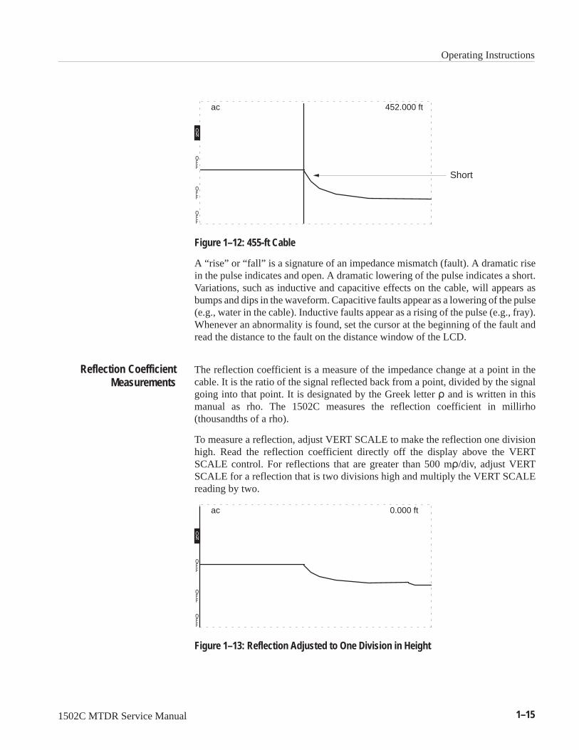
A “rise” or “fall” is a signature of an impedance mismatch (fault). A dramatic risein the pulse indicates and open. A dramatic lowering of the pulse indicates a short.Variations, such as inductive and capacitive effects on the cable, will appears asbumps and dips in the waveform. Capacitive faults appear as a lowering of the pulse(e.g., water in the cable). Inductive faults appear as a rising of the pulse (e.g., fray).Whenever an abnormality is found, set the cursor at the beginning of the fault andread the distance to the fault on the distance window of the LCD.
The reflection coefficient is a measure of the impedance change at a point in thecable. It is the ratio of the signal reflected back from a point, divided by the signalgoing into that point. It is designated by the Greek letter and is written in thismanual as rho. The 1502C measures the reflection coefficient in millirho(thousandths of a rho).
To measure a reflection, adjust VERT SCALE to make the reflection one divisionhigh. Read the reflection coefficient directly off the display above the VERTSCALE control. For reflections that are greater than 500 m/div, adjust VERTSCALE for a reflection that is two divisions high and multiply the VERT SCALEreading by two.
OFF
OFF
OFF
ON
ac 0.000 ft
Figure 1–13: Reflection Adjusted to One Division in Height
Reflection CoefficientMeasurements

Operating Instructions
1–16 1502C MTDR Service Manual
In an ideal transmission system with no changes in impedance, there will be noreflections, so rho is equal to zero. A good cable that is terminated in itscharacteristic impedance is close to ideal and will appear as a flat line on the 1502Cdisplay.
Small impedance changes, like those from a connector, might have reflections from10 to 100 m. If rho is positive, it indicates an impedance higher than that of thecable before the reflection. It will show as an upward shift or bump on the waveform.If rho is negative, it indicates an impedance lower than that of the cable prior to thereflection. It will show as a downward shift or dip on the waveform.
If the cable has an open or short, all the energy sent out by the 1502C will bereflected. This is a reflection coefficient of rho = 1, or +1000 m for the open and–1000 m for the short.
Long cables have enough loss to affect the size of reflections. In the 1502C, this losswill usually be apparent as an upward ramping of the waveform along the length ofthe cable. In some cases, the reflection coefficient measurement can be corrected forthis loss. This correction can be made using a procedure very similar to the VerticalCompensation for Higher Impedance Cable procedure (see the VERT SET REFsection).
Return loss is another was of measuring impedance changes in a cable.Mathematically, return loss is related to rho by the formula:
Return Loss (in dB) = –20 * log (base ten) of Absolute Value of Rho (Vref/Vinc)
The 1502C can be made to display in dB instead of m/div through the menu:
1. Press MENU.
2. Select Setup Menu.
3. Press MENU again.
4. Select Vertical Scale is: Millirho.
5. Press MENU again. This should change is to Vertical Scale is: Decibels.
6. Press MENU twice to return to normal operation.
To measure return loss with the 1502C, adjust the height of the reflected pulse tobe two divisions high and read the dB return loss directly off the LCD. The incidentpulse is set to be two divisions high at zero dB automatically when the instrumentis turned on.
Return LossMeasurements

Operating Instructions
1502C MTDR Service Manual 1–17
OFF
OFF
OFF
ON
ac 0.000 ft
Figure 1–14: Return Loss
A large return loss means that most of the pulse energy was lost instead of beingreturned as a reflection. The lost energy might have been sent down the cable orabsorbed by a terminator or load on the cable. A terminator matched to the cablewould absorb most of the pulse, so its return loss would be large. An open or shortwould reflect all the energy, so its return loss would be zero.
The 1502C can compute and display what impedance mismatch would cause areflection as high (or low) as the point at the cursor. This measurement is useful forevaluating the first impedance mismatch (first reflection) or small impedancechanges along the cable (e.g., connectors, splices).
This function can be selected in the Setup Menu. Once it is enabled, the impedancevalue will be displayed under the distance in the distance window.
OFF
OFF
OFF
ON
acOhms-at-Cursor
2.800 ft50.0
Readout
Figure 1–15: Ohms-at-Cursor
The accuracy of the difference measurement in impedance between two points neareach other is much better than the absolute accuracy of any single pointmeasurement. For example, a cable might vary from 51.3 to 58.4 across aconnector – the 7.1 difference is accurate to about 2%. The 51.3 measurementby itself is only specified to be accurate to 10%.
Ohms-at-Cursor

Operating Instructions
1–18 1502C MTDR Service Manual
The series resistance of the cable to the point at the cursor affects the accuracy ofthe impedance measurement directly. In a cable with no large impedance changes,the series resistance is added to the reading. For example, the near end of a long 50 coaxial cable might read 51.5 , but increase to 57.5 several hundred feet alongthe cable. The 6 difference is due to the series resistance of the cable, not to achange in the actual impedance of the cable.
Another limitation to the ohms-at-cursor function is that energy is lost going bothdirections through a fault. This will cause readings of points farther down the cableto be less accurate than points nearer to the instrument.
In general, it is not wise to try to make absolute measurements past faults becausethe larger the fault, the less accurate those measurements will be. Although they donot appear as faults, resistive pads (often used to match cable impedances) alsoaffect measurements this way.
When pushed, the VIEW INPUT button displays the input at the front panel CABLEconnector. When VIEW INPUT is turned off and no other buttons are pushed, thedisplay will not have a waveform on it (see Figure 1–16). The default conditionwhen the instrument is powered up is to have VIEW INPUT on.
OFF
OFF
OFF
ac 0.000 ft
OFF
Figure 1–16: Display with VIEW INPUT Turned Off
When pushed, the STORE button puts the current waveform being displayed intomemory. If already stored, pushing STORE again will erase the stored waveform.
The front panel control settings and the menu-accessed settings are also stored. Theyare accessed under View Stored Waveform Settings in the first level of the menu.
Using VIEW INPUT
How to Store theWaveform

Operating Instructions
1502C MTDR Service Manual 1–19
OFF
OFF
ON
ac 3.000 ft
ON
Figure 1–17: Display of a Stored Waveform
The VIEW STORE button, when pushed on, displays the waveform stored in thememory as a dotted line. If there is no waveform in memory, a message appears onthe LCD informing you of this.
OFF
ac 3.000 ft
ON
ON
OFF
Figure 1–18: Display of a Stored Waveform
When pushed on, the VIEW DIFF button displays the difference between the currentwaveform and the stored waveform as a dotted line. If no waveform has been stored,a message will appear. The difference waveform is made by subtracting each pointin the stored waveform from each point in the current waveform.
NOTE. If the two waveforms are identical (e.g., if STORE is pushed and VIEW DIFFis immediately pushed) the difference would be zero. Therefore you would see thedifference waveform as a straight line.
The VIEW DIFF waveform will move up and down with the current input as youmove the
POSITION control. Any of the waveforms may be turned on or off
independently. You might want to turn off some waveforms if the display becomestoo busy or confusing.
Using VIEW STORE
Using VIEW DIFF
Operating Instructions
1–20 1502C MTDR Service Manual
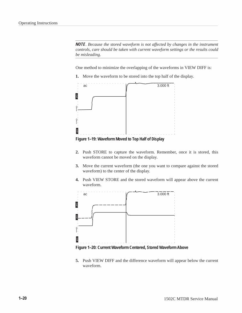
NOTE. Because the stored waveform is not affected by changes in the instrumentcontrols, care should be taken with current waveform settings or the results couldbe misleading.
One method to minimize the overlapping of the waveforms in VIEW DIFF is:
1. Move the waveform to be stored into the top half of the display.
OFF
OFF
ON
ac 3.000 ft
ON
Figure 1–19: Waveform Moved to Top Half of Display
2. Push STORE to capture the waveform. Remember, once it is stored, thiswaveform cannot be moved on the display.
3. Move the current waveform (the one you want to compare against the storedwaveform) to the center of the display.
4. Push VIEW STORE and the stored waveform will appear above the currentwaveform.
OFF
ON
ac 3.000 ft
ON
ON
Figure 1–20: Current Waveform Centered, Stored Waveform Above
5. Push VIEW DIFF and the difference waveform will appear below the currentwaveform.

Operating Instructions
1502C MTDR Service Manual 1–21
ON
ac 3.000 ft
ON
ON
ON
Stored WaveformVIEW STORE
Current Waveform
Difference
VIEW INPUT
VIEW DIFF
Figure 1–21: Current Waveform Center, Stored Waveform Above, Difference Below
Notice the VIEW INPUT waveform is solid, VIEW DIFF is dotted, and VIEWSTORE is dot-dash.
There are many situations where the VIEW DIFF function can be useful. Onecommon situation is to store the waveform of a suspect cable, repair the cable, thencompare the two waveforms after the repair. During repairs, the VIEW INPUT,VIEW DIFF, and VIEW STORE waveforms can be used to judge the effectivenessof the repairs. The optional chart recorder can be used to make a chart of the threewaveforms to document the repair.
Another valuable use for the VIEW DIFF function is for verifying cable integritybefore and after servicing or periodic maintenance that requires moving ordisconnecting the cable.
The VIEW DIFF function is useful when you want to see any changes in the cable.In some systems, there might be several reflections coming back from each branchof the network. It might become necessary to disconnect branch lines from the cableunder test to determine whether a waveform represents a physical fault or is simplyan echo from one of the branches. The STORE and VIEW DIFF functions allow youto see and compare the network with and without branches.
Two important things to be observed when using the VIEW DIFF function:
If you change either the VERT SCALE or DIST/DIV, you will no longer becomparing features that are the same distance apart or of the same magnitudeon the display. It is possible to save a feature (e.g., a connector or tap) at onedistance down the cable and compare it to a similar feature at a different distanceby moving the
POSITION and
POSITION controls.
When this is done, great care should be taken to make sure the vertical andhorizontal scales are identical for the two waveforms being compared. If eitherthe stored or current waveform is clipped at the top or bottom of the display, thedifference waveform will be affected.

Operating Instructions
1–22 1502C MTDR Service Manual
HORZ SET REF ( mode) allows you to offset the distance reading. For example,a lead-in cable to a switching network is three feet long and you desire to start themeasurement after the end of the lead-in cable. HORZ SET REF makes it simple.
OFF
OFF
OFF
ON
ac 0.000 ft
End of3-ft cable
Figure 1–22: Waveform of Three-Foot Lead-in Cable
1. Turn the NOISE FILTER control to HORZ SET REF. The noise readout on theLCD will show: set .
2. Turn the
POSITION control to set the cursor where you want to start thedistance reading. This will be the new zero reference point. For a three-footlead-in cable, the cursor should be set at 3.00 ft.
OFF
OFF
OFF
ON
ac 3.000 ft
Figure 1–23: Cursor Moved to End of Three-Foot Lead-in Cable
3. Push STORE.
4. Turn the NOISE FILTER control to 1 avg. The instrument is now in HORZ SETREF, or delta mode. The distance window should now read 0.00 ft. As the cursoris scrolled down the cable, the distance reading will now be from the new zeroreference point.
Using Horizontal SetReference

Operating Instructions
1502C MTDR Service Manual 1–23
OFF
OFF
OFF
ON
ac 0.000 ft
Figure 1–24: Cursor Moved to End of Three-Foot Lead-in Cable
NOTE. Vp changes will affect where the reference is set on the cable. Be sure to setthe Vp first, then set the delta to the desired location.
5. To exit HORZ SET REF, use the following procedure:
a. Turn the NOISE FILTER control to HORZ SET REF.
b. Turn DIST/DIV to .1 ft/div. If the distance reading is extremely high, youmight want to use a higher setting initially, then turn to .1 ft/div for the nextadjustment.
c. Turn the
POSITION control until the distance window reads 0.00 ft.
OFF
OFF
OFF
ON
ac 0.000 ft
Figure 1–25: Cursor Moved to 0.00 ft
d. Push STORE.
e. Turn NOISE FILTER to desired setting.
VERT SET REF works similar to HORZ SET REF except that it sets a referencefor gain (pulse height) instead of distance. This feature allows zeroing the dB scaleat whatever pulse height is desired.
1. Turn NOISE FILTER fully counterclockwise. “Set Ref” will appear in the noiseaveraging area of the LCD.
Using Vertical SetReference
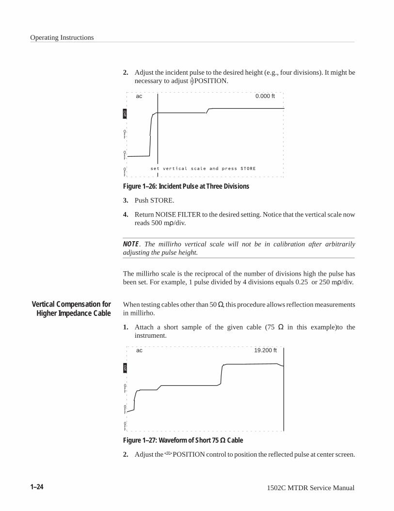
Operating Instructions
1–24 1502C MTDR Service Manual
2. Adjust the incident pulse to the desired height (e.g., four divisions). It might benecessary to adjust
POSITION.
OFF
OFF
OFF
ON
ac 0.000 ft
Figure 1–26: Incident Pulse at Three Divisions
3. Push STORE.
4. Return NOISE FILTER to the desired setting. Notice that the vertical scale nowreads 500 m/div.
NOTE. The millirho vertical scale will not be in calibration after arbitrarilyadjusting the pulse height.
The millirho scale is the reciprocal of the number of divisions high the pulse hasbeen set. For example, 1 pulse divided by 4 divisions equals 0.25 or 250 m/div.
When testing cables other than 50 , this procedure allows reflection measurementsin millirho.
1. Attach a short sample of the given cable (75 in this example)to theinstrument.
OFF
OFF
OFF
ON
ac 19.200 ft
Figure 1–27: Waveform of Short 75 Cable
2. Adjust the
POSITION control to position the reflected pulse at center screen.
Vertical Compensation forHigher Impedance Cable

Operating Instructions
1502C MTDR Service Manual 1–25
3. Turn NOISE FILTER to VERT SET REF.
4. Adjust VERT SCALE so the reflected pulse (from open at far end of cablesample) is two divisions high.
OFF
OFF
OFF
ON
ac 19.200 ft
Figure 1–28: Waveform Centered and Adjusted Vertically
5. Press STORE.
6. Return NOISE FILTER to the desired setting.
7. Adjust the
POSITION control to the desired position on the waveform tomeasure loss.
OFF
OFF
OFF
ON
ac 1.840 ft
Figure 1–29: Cursor Moved to Desired Position
The instrument is now set to measure reflections in millirho relative to the samplecable impedance.
To measure reflections on a 50 cable, the VERT SET REF must be reset.
8. To exit VERT SET REF, use the following procedure:
a. Turn NOISE FILTER to VERT SET REF.
b. Adjust VERT SCALE to obtain an incident pulse height of two divisions.
c. Push STORE.

Operating Instructions
1–26 1502C MTDR Service Manual
d. Turn NOISE FILTER to desire filter setting.
The instrument can be turned off and back on to default to the two division pulseheight.
Additional Features (Menu Selected)
The 1502C will capture and store waveforms on an ongoing basis. This is usefulwhen the cable or wire is subjected to intermittent or periodic conditions. The 1502Cwill monitor the line and display any fluctuations on the LCD.
1. Attach the cable to the 1502C front-panel CABLE connector.
2. Push MENU to access the main menu.
3. Scroll to Setup Menu and push MENU again.
4. Scroll to Acquisition Control Menu and push MENU again.
5. Scroll to Max Hold is: Off and push MENU again. This line will change to MaxHold is: On. The monitoring function is now ready to activate.
6. Repeatedly push MENU until the instrument returns to normal operation.
ON
ac 0.000 ft
OFF
Figure 1–30: Waveform Viewed in Normal Operation
7. When you are ready to monitor this cable for intermittents, push STORE. The1502C will now capture any changes in the cable.
Max Hold

Operating Instructions
1502C MTDR Service Manual 1–27
ON
ac 0.000 ft
ON
Capturedchanges
Figure 1–31: Waveform Showing Intermittent Changes
8. To exit monitor mode, push STORE again.
9. To exit Max Hold, access the Acquisition Control Menu again, turn off MaxHold, and push MENU repeatedly until the instrument returns to normaloperation.
This feature puts the 1502C in a “listening mode” by turning off the pulse generator.
1. Attach a cable to the 1502C front-panel CABLE connector.
2. Push MENU to access the Main Menu.
3. Scroll to Setup Menu and push MENU again.
4. Scroll to Acquisition Control Menu and push MENU again.
5. Scroll to Pulse is: On and push MENU again. This will change to Pulse is: Off.
OFF
OFF
OFF
ON
ac 0.000 ft
Figure 1–32: Waveform Display with No Outgoing Pulses
6. Repeatedly press MENU until the instrument returns to normal operation.
Pulse On/Off

Operating Instructions
1–28 1502C MTDR Service Manual
CAUTION. This function is used mostly for troubleshooting by qualified technicians.It is not recommended that you use the 1502C as a stand-alone monitoring device.The input circuitry is very sensitive and can be easily damaged by even moderatelevel signals.
NOTE. In this mode, the 1502C is acting as a detector only. Any pulses detected willnot originate from the instrument, so any distance readings will be invalid. If youare listening to a local area network, for example, it is possible to detect traffic, butnot possible to measure the distance to its origin.
Pulse is: Off can be used in conjunction with Max Hold is: On.
7. To exit Pulse is: Off, access the Acquisition Control Menu again, turn pulse backon, then push MENU until the instrument returns to normal operation.
The single sweep function will acquire one waveform only and display it.
1. Attach a cable to the 1502C front-panel CABLE connector.
2. Push MENU to access the Main Menu.
3. Scroll to Setup Menu and push MENU again.
4. Scroll to Acquisition Control Menu and push MENU again.
5. Scroll to Single Sweep is: Off and push MENU again. This will change to SingleSweep is: On.
6. Repeatedly press MENU until the instrument returns to normal operation.
7. When you are ready to begin a sweep, push VIEW INPUT. A sweep will alsobe initiated when you change any of the front-panel controls. This allows youto observe front panel changes without exiting the Single Sweep mode.
As in normal operation, averaged waveforms will take longer to acquire.
Single Sweep

Operating Instructions
1502C MTDR Service Manual 1–29
OFF
OFF
OFF
ac 0.000 ft
OFF
Figure 1–33: A Captured Single Sweep
8. To exit Single Sweep is: On, access the Acquisition Control Menu again, turnthe Single Sweep back off, then repeatedly push MENU until the instrumentreturns to normal operation.

Operating Instructions
1–30 1502C MTDR Service Manual
1502C MTDR Service Manual 2–1
Operator Performance Checks
This chapter contains performance checks for many of the functions of the 1502C.They are recommended for incoming inspections to verify that the instrument isfunctioning properly. Procedures to verify the actual performance requirements areprovided in chapter 6.
Performing these checks will assure you that your instrument is in good workingcondition. These checks should be performed upon receipt of a new instrument orone that has been serviced or repaired. It does not test all portions of the instrumentto Calibration specifications.
The purpose of these checks is not to familiarize a new operator with the instrument.If you are not experienced with the instrument, you should read the OperatingInstructions chapter of this manual before going on with these checks.
If the instrument fails any of these checks, it should be serviced. Many failure modesaffect only some of the instrument functions.
Item Tektronix Part Number
50 precision terminator 011–0123–00
3-foot precision coaxial cable 012–1350–00
Disconnect any cables from the front-panel CABLE connector. Connect theinstrument to a suitable power source (a fully charged optional battery pack or ACline source). If you are using AC power, make sure the fuse and power switch arecorrect for the voltage you are using (115 VAC requires a different fuse than230 VAC).
Pull the POWER switch on the front panel. If a message does not appear on thedisplay within a second or two, turn the instrument off. There are some failure modesthat could permanently damage or ruin the LCD if the power is left on for more thana minute or so.
Option 05 instruments default to metric; however, you can change the metric scaleto ft/div in the Setup Menu or use the metric numbers provided. To change thereadings, press the MENU button. Using the
POSITION control, scroll down to
Setup Menu and press MENU again. Scroll down to Distance/Div is: m/div and pressMENU again. This will change to ft/div. Press the MENU button repeatedly toreturn to normal operation mode. If the instrument power is turned off, these checksmust be repeated again when the instrument is powered on again.
Equipment Required
Getting Ready
Power On
Metric Instruments

Operator Performance Checks
2–2 1502C MTDR Service Manual
Set the 1502C front-panel controls:
NOISE FILTER 1 avgVERT SCALE defaultDIST/DIV 1 ft/div (0.25 m)Vp .66
If the instrument fails this check, it must be repaired before any distancemeasurements can be made with it.
1. Turn the 1502C power on. The display should look very similar to Figure B–1.
OFF
OFF
OFF
ON
ac 0.000 ft
Figure 2–1: Start-up Measurement Display
2. Connect the 3-foot precision cable to the front-panel CABLE connector. Thedisplay should now look like Figure B–2.
ON
ac 0.000 ft
OFF
OFF
OFF
Figure 2–2: Measurement Display with 3-foot Cable
3. Using the
POSITION control, measure the distance to the rising edge of thewaveform at the open end of the cable. The distance shown on the displaydistance window (upper right corner of the LCD) should be from 2.87 to 3.13feet (0.875 to 0.954 m).
Set Up
1. Horizontal Scale(Timebase) Check

Operator Performance Checks
1502C MTDR Service Manual 2–3
ON
ac 3.000 ft
OFF
OFF
OFF
Figure 2–3: Cursor at End of 3-foot Cable
4. Remove the 3-foot cable and connect the 50 terminator.
5. Change the DIST/DIV to 200 ft/div (50 m/div)
6. Turn the
POSITION control clockwise until the distance window shows adistance greater than 2,000 feet (> 600 m). The waveform should be a flat linefrom the pulse to this point.
OFF
OFF
OFF
ON
ac 2051.000 ft
Figure 2–4: Flat-Line Display Out to 50,000+ Feet
7. Turn the
POSITION control counterclockwise until the distance windowshows a distance less than 10.000 feet (< 3.1 m).
8. Set the DIST/DIV control to .1 ft/div (0.025 m/div).
9. Turn the
POSITION control counterclockwise until the distance windowshows a distance of –2.000 feet (–0.611 m).
Operator Performance Checks
2–4 1502C MTDR Service Manual
OFF
OFF
OFF
ON
ac –2.000 ft
Figure 2–5: Flat-Line Display at –2.000 ft
This last step has set up the instrument for the next check.
If the instrument fails this test, it can be used, but should be serviced when possible.Not all of the waveforms will be viewable at all gain settings.
1. Using the
POSITION control, verify that the entire waveform can be movedto the very top of the display (off the graticule area).
OFF
OFF
OFF
ON
ac –2.000 ftWaveformoff display
Figure 2–6: Waveform Off the Top of the Display
2. Using the
POSITION control, verify that the entire waveform can be movedto the very bottom of the display (to the bottom graticule line).
2. Vertical Position(Offset) Check

Operator Performance Checks
1502C MTDR Service Manual 2–5
OFF
OFF
OFF
ON
ac –2.000 ft
Waveform
Figure 2–7: Waveform at the Bottom of the Display
If the instrument fails this check, it can still be usable for measurements of largefaults that do not require a lot of gain, but send the instrument to be serviced whenpossible. A great deal of noise reduction can be made using the NOISE FILTERcontrol.
1. Adjust the
POSITION control to obtain 100.000 ft in the distance window.
ON
ac 100.000 ft
OFF
OFF
OFF
Figure 2–8: Waveform with Gain at 5.00 m/div
2. Using the
POSITION control and VERT SCALE control, set the gain to 5.00m/div. Keep the waveform centered vertically in the display.
3. Press MENU.
4. Using the
POSITION control, select Diagnostics Menu.
5. Press MENU again.
6. Using the
POSITION control, select Service Diagnostic Menu.
7. Press MENU again.
8. Using the
POSITION control, select Noise Diagnostics.
9. Press MENU again and follow the instructions on the display.
3. Noise Check

Operator Performance Checks
2–6 1502C MTDR Service Manual
10. Exit from Noise Diagnostics, but do not exit from the Service Diagnostic Menuyet.
If the instrument fails this check, it should not be used for loss or impedancemeasurements. Send it to be serviced when possible.
1. In the Service Diagnostic Menu, select the Offset/Gain Diagnostic and followthe directions on the display.
NOTE. Occasionally, the instrument might not pass the 48 dB step. This is no causefor alarm. If the remainder of the steps do not fail, proceed as normal. Refer to the1502C Service Manual for additional information.
There are three screens of data presented in this diagnostic. The Pass/Fail level is3% for any single gain setting tested.
2. Exit from Offset/Gain Diagnostic, but do not leave the Service DiagnosticMenu yet.
If the instrument fails this check, the waveforms might not look normal. If theefficiency is more than 100%, the waveforms will appear noisy. If the efficiency isbelow the lower limit, the waveform will take longer (more pixels) to move fromthe bottom to the top of the reflected pulse. This smoothing effect might completelyhide some faults that would normally only be one or two pixels wide on the display.
1. In the Service Diagnostic Menu, select Sampling Efficiency and follow thedirections on the screen.
2. When done with the test, press the MENU button repeatedly until the instrumentreturns to normal operation.
If the aberrations are out of specification, the ohms-at-cursor function might be lessaccurate than specified.
1. Connect the 50 precision terminator to the front-panel CABLE connector.
2. Set the DIST/DIV control to 5 ft/div (1 m/div).
3. Increase the VERT SCALE control to 50 m/div.
4. Using the
POSITION control, move the top of the pulse to the center graticuleline.
4. Offset/Gain Check
5. Sampling EfficiencyCheck
6. Aberrations Check

Operator Performance Checks
1502C MTDR Service Manual 2–7
ON
ac –2.000 ft
OFF
OFF
OFF
Figure 2–9: Top of Pulse on Center Graticule
5. Set the DIST/DIV control to 0.2 ft/div (0.05 m/div).
6. Turn the
POSITION control clockwise until the rising edge of the incidentpulse is in the left-most major division on the display.
ON
ac 1.160 ft
OFF
OFF
OFF
Figure 2–10: Rising Edge of Incident Pulse in Left-most Major Division
7. Using the
POSITION control, move the cursor back to 0.000 ft (0.00 m).
All the aberrations, except the one under the cursor (see Figure 2–11), must bewithin one division of the center graticule line from out to 10 feet past the risingedge of the pulse.
To verify distances past the right edge of the display, scroll along the waveformby turning the
POSITION control clockwise.

Operator Performance Checks
2–8 1502C MTDR Service Manual
ON
ac 0.000 ft
OFF
OFF
OFF
Figure 2–11: Waveform Centered, Cursor at 0.000 ft
If the risetime is out of specification, it might be difficult to make accurateshort-distance measurements near the front panel.
1. Set the 1502C front-panel controls:
NOISE FILTER 1 avgVERT SCALE 500 m/divDIST/DIV 0.2 ft/div (0.05 m)Vp .99
2. Using the
POSITION control, move the incident pulse to the center of thedisplay as shown below.
OFF
OFF
OFF
ON
ac –1.432 ft
Figure 2–12: Pulse Centered on Display
3. Turn the VERT SCALE control clockwise until the leading edge of the incidentpulse is five major divisions high (about 205 m).
4. Position the waveform so that it is centered about the middle graticule line.
7. Risetime Check

Operator Performance Checks
1502C MTDR Service Manual 2–9
OFF
OFF
OFF
ON
ac –0.848 ft
CrossesLowestPoint
Figure 2–13: Cursor on Lowest Major Graticule that Rising Edge Crosses
5. Using the
POSITION control, and noting the distances displayed, verify thatthe distance between the points where the leading edge crosses the highest andlowest major graticule lines is less than or equal to 0.096 feet (0.029 m).
OFF
OFF
OFF
ON
ac –0.768 ft
CrossesHighestPoint
Figure 2–14: Cursor on Highest Major Graticule that Rising Edge Crosses
In the above example, the distances are –0.848 feet and –0.768 feet. The differencebetween these two measurements is 0.080 feet, which is well within specification.
Jitter is the uncertainty in the timebase. Its main effect is that the waveform appearsto move back and forth a very small amount. If the jitter is too great, it will affectthe repeatability of very precise distance measurements.
1. Set the VERT SCALE less than or equal to 1.0 m/div.
2. Watch the leading edge of the pulse move and verify that this movement is lessthan five pixels, or < 0.02 ft (0.006 m).
8. Jitter Check

Operator Performance Checks
2–10 1502C MTDR Service Manual
OFF
OFF
OFF
ON
ac –1.624 ft
Jitter
Figure 2–15: Jitter Apparent on Leading Edge of Incident Pulse
Using the Max Hold function (accessed in the Setup Menu, Acquisition Control) cansimplify your observation of jitter. Max Hold allows you to observe the accumulatedjitter without having to stare continuously at the display.
OFF
OFF
OFF
ON
ac –1.624 ft
JitterAccumulated
Figure 2–16: Jitter Captured Using Max Hold
If the instrument failed Jitter or Risetime checks, it is probably still adequate for allbut extremely precise distance measurements. If it failed the Horizontal Scale check,you should not use the instrument until the cause of the failure has been identifiedand corrected.
All of the previous checks only test the major functional blocks of the instrumentthat could prevent you from being able to make measurements. It is possible for thefront-panel controls or the LCD to have problems that would interfere withcontrolling or displaying measurements. Most problems of this type would becomeevident as you perform the checks. If you suspect a problem of this nature, youshould have the instrument checked by a qualified service technician, using thediagnostics in the 1502C Service Manual.
If the instrument passed all of the previous checks, it is ready for use.
Conclusions
1502C MTDR Service Manual 3–1
Specifications
The tables in this chapter list the characteristics and features that apply to thisinstrument after it has had a warm-up period of at least five minutes.
The Performance Requirement column describes the limits of the Characteristic.Supplemental Information describes features and typical values or other helpfulinformation.
Electrical Characteristics
Characteristic Performance Requirement Supplemental Information
Excitation PulseReflected Pulse 200 ps (0.096 feet) Vp set to 0.99; 10 to 90%, into a precision short
Aberrations 5% peak within 0 to 10 feet after rise0.5% peak beyond 10 feet
Excluding front panel BNC
Jitter 0.02 feet (40 ps) p-p Horz scale 0.1 ft/div0.2 feet (400 ps) p-p Horz scale 1 ft/div
Vp set to 0.99, DIST/DIV set to 0.1 ft/divAt 23.4 feet to 46.8 feet, jitter is 0.4 feet.
Output Impedance 50 nominal While pulse is on, typically 2%Pulse Amplitude 300 mV nominal into 50 load
Pulse Width 25 s nominal
Pulse Repetition Time 200 s nominal
VerticalScales
Accuracy
Set Adj
0.5 m/div to 500 m/div,
Within 3% of full scale
> 240 values, includes 1, 2, 5 sequences(accuracy depends on reference level)
Set incident pulse within 3%. Combined withVERT SCALE control.
Vertical Position Any waveform point is moveable to center screen
Displayed Noise 5 m peak or less, filter set to 12 m peak or less, filter set to 8
Distance CursorResolution 1/25th of 1 major division
Cursor ReadoutRangeResolution
–2 ft to 2,000 ft0.004 ft
Distance MeasurementAccuracy 1.6 inches or 1% of distance measured,
whichever is greater
For cables with Vp = 0.66For delta mode measurementsError 0.5% for distance 27 ftError 1.0% for distance 14 ftError 2.0% for distance 7 ftError 10% for distance 1.5 ft
(continued next page)
Specifications
3–2 1502C MTDR Service Manual
Characteristic Performance Requirement Supplemental Information
Cursor Ohms ReadoutRange
Resolution
Accuracy
1 to 1 k
3 significant digits
10% with serial cable impedancecorrection (relative impedancemeasurements 2%)
HorizontalScales
Range
0.1 ft/div to 200 ft/div (0.025 m/div to 50 m/div)11 values, 1, 2, 5 sequence1 ft to 2,000 ft (2.5 m to 500 m)
Horizontal Position Any distance to full scale can be moved onscreen
VpRange
Resolution
Accuracy Within 1%
Propagation velocity relative to air0.30 to 0.99
0.01
Custom Option Port Tektronix Chart Recorders YT–1 and YT–1S aredesigned to operate with the 1502C. Produces ahigh resolution thermal dot matrix recording ofwaveform and switch values.
Line Voltage 115 VAC (90 to 132 VAC) 45 to 440 Hz, or230 VAC (180 to 250 VAC) 45 to 440 Hz, or12 VDC through battery pack connector
Fused at 0.3 A (0.3 A, 250 V, T)Fused at 0.15 A (0.15 A, 250 V, T)
Battery Operation
Full Charge Time
Overcharge Protection
Discharge Protection
Charge Capacity
Charge Indicator
5 hours minimum, 20 chart recordings maxi-mum
+15° C to +25° C charge and discharge temp,LCD backlight off. Operation of instrument withbacklight on or at temps below +10° C will degrade battery operation specification
20 hours maximum
Limited to 10 days continuous charge. Batterywill charge whenever instrument is plugged in.Battery can be removed during AC operation.
Operation terminates prior to cell reversal
2 Amp-hours typical
Bat/low will be indicated on LCD when capacityreaches approximately 10%

Specifications
1502C MTDR Service Manual 3–3
Environmental Characteristics
Characteristic Performance Requirement Supplemental Information
TemperatureOperating
Non-operating
–10° C to +55° C
–62° C to +85° C
Battery capacity reduced at other than +15°C to+25°C
With battery removed. Storage temp with bat-tery in is –20° C to +55° C. Contents on non-volatile memory (stored waveform) might be lostat temps below –40° C.
Humidity to 100%
AltitudeOperating
Non-operating
to 10,000 ft
to 40,000 ft
MIL–T–28800C, Class 3
Vibration 5 to 15 Hz, 0.06 inch p–p15 to 25 Hz, 0.04 inch p–p25 to 55 Hz, 0.013 inch p–p
MIL–T–28800C, Class 3
Shock, MechanicalPulse
Bench Handling
Operating
Non-operating
30 g, 11 ms 1/2 sine wave, total of 18 shocks
4 drops each face at 4 inches or 45 degreeswith opposite edge as pivot
4 drops each face at 4 inches or 45 degreeswith opposite edge as pivot. Satisfactory opera-tion after drops.
MIL–T–28800C, Class 3
MIL–STD–810, Method 516, Procedure V
Cabinet on, front cover off
Cabinet off, front cover off
Loose Cargo Bounce 1 inch double-amplitude orbital path at 5 Hz, 6 faces
MIL–STD–810, Method 514, Procedure XI,Part 2
Water ResistanceOperating
Non-operating
Splash-proof and drip-proof
Watertight with 3 feet of water above top of case
MIL–T–28800C, Style AFront cover off
Front cover on
Salt Atmosphere Withstand 48 hours, 20% solution withoutcorrosion
Sand and Dust Operates after test with cover on, non-operating MIL–STD–810, Method 510, Procedure I
Washability Capable of being washed
Fungus Inert Materials are fungus inert
(continued next page)

Specifications
3–4 1502C MTDR Service Manual
Certifications and Compliances
Category Standard or description
EC Declaration of Conformity –EMC
Meets intent of Directive 89/336/EEC for Electromagnetic Compatibility. Compliance was demonstratedto the following specifications as listed in the Official Journal of the European Union:
EN 50081-1 Emissions:EN 55022 Class B Radiated and Conducted EmissionsEN 60555-2 AC Power Line Harmonic Emissions
EN 50082-1 Immunity:IEC 801-2 Electrostatic Discharge ImmunityIEC 801-3 RF Electromagnetic Field ImmunityIEC 801-4 Electrical Fast Transient/Burst ImmunityIEC 801-5 Power Line Surge Immunity
Australia/New ZealandDeclaration of Conformity – EMC
Complies with EMC provision of Radiocommunications Act per the following standard(s):
AS/NZS 2064.1/2 Industrial, Scientific, and Medical Equipment: 1992EMC Compliance Meets the intent of Directive 89/336/EEC for Electromagnetic Compatibility when it is used with the
product(s) stated in the specifications table. Refer to the EMC specification published for the statedproducts. May not meet the intent of the directive if used with other products.
FCC Compliance Emissions comply with FCC Code of Federal Regulations 47, Part 15, Subpart B, Class A Limits.Safety Standards
U.S. Nationally Recognized Testing Laboratory Listing
UL1244 Standard for electrical and electronic measuring and test equipment.
Canadian Certification CAN/CSA C22.2 No. 231 CSA safety requirements for electrical and electronic measuring and test equipment.
European Union Compliance Low Voltage Directive 73/23/EEC, amended by 93/68/EEC
EN 61010-1/A2 Safety requirements for electrical equipment for measurement,control, and laboratory use.
Additional Compliance IEC61010-1/A2 Safety requirements for electrical equipment for measurement, control, and laboratory use.
Safety Certification ComplianceEquipment Type Test and measuringSafety Class Class 1 (as defined in IEC 61010-1, Annex H) – grounded productOvervoltage Category Overvoltage Category II (as defined in IEC 61010-1, Annex J)Pollution Degree Pollution Degree 3 (as defined in IEC 61010-1).
Installation (Overvoltage)Category
Terminals on this product may have different installation (overvoltage) category designations. Theinstallation categories are:
CAT III Distribution-level mains (usually permanently connected). Equipment at this level is typically in a fixed industrial location.
CAT II Local-level mains (wall sockets). Equipment at this level includes appliances, portable tools, and similar products. Equipment is usually cord-connected.
CAT I Secondary (signal level) or battery operated circuits of electronic equipment.
(continued next page)
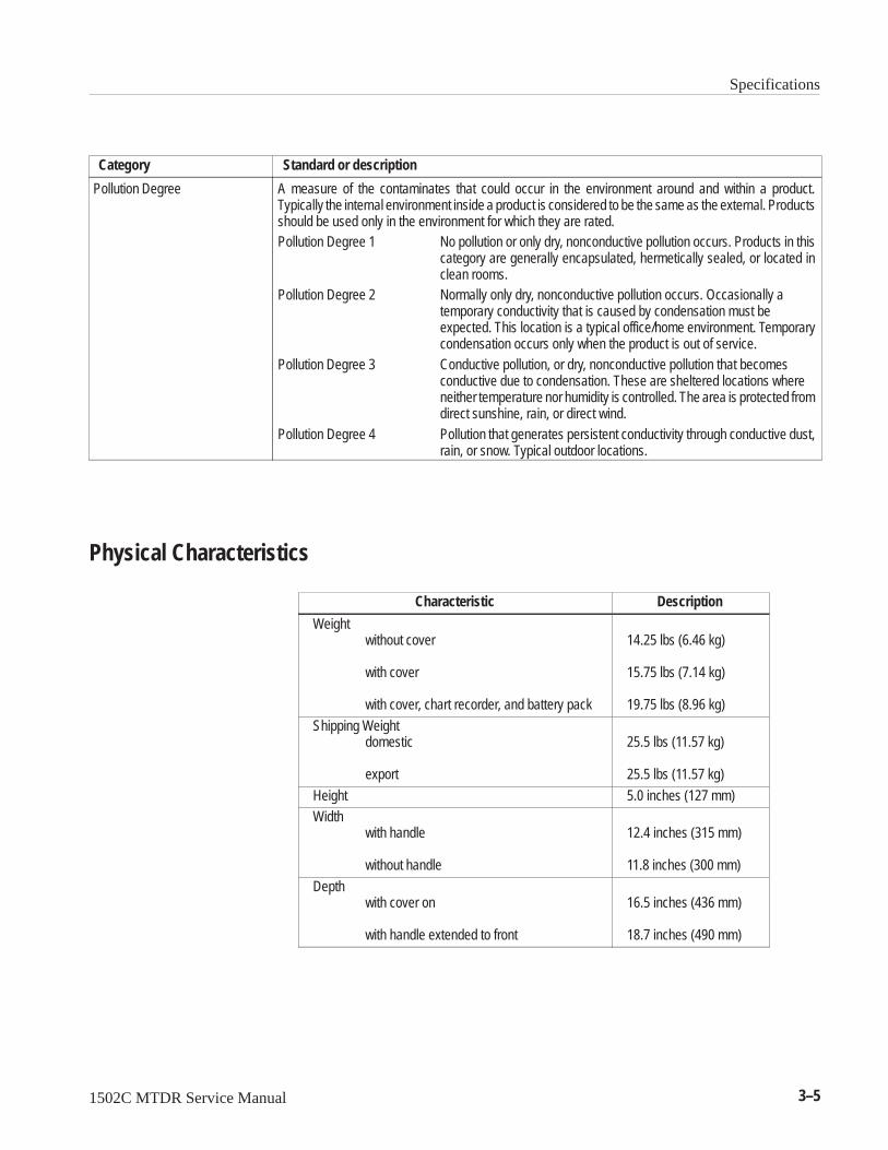
Specifications
1502C MTDR Service Manual 3–5
Category Standard or description
Pollution Degree A measure of the contaminates that could occur in the environment around and within a product.Typically the internal environment inside a product is considered to be the same as the external. Productsshould be used only in the environment for which they are rated.Pollution Degree 1 No pollution or only dry, nonconductive pollution occurs. Products in this
category are generally encapsulated, hermetically sealed, or located inclean rooms.
Pollution Degree 2 Normally only dry, nonconductive pollution occurs. Occasionally a temporary conductivity that is caused by condensation must be expected. This location is a typical office/home environment. Temporarycondensation occurs only when the product is out of service.
Pollution Degree 3 Conductive pollution, or dry, nonconductive pollution that becomes conductive due to condensation. These are sheltered locations where neither temperature nor humidity is controlled. The area is protected fromdirect sunshine, rain, or direct wind.
Pollution Degree 4 Pollution that generates persistent conductivity through conductive dust,rain, or snow. Typical outdoor locations.
Physical Characteristics
Characteristic Description
Weightwithout cover
with cover
with cover, chart recorder, and battery pack
14.25 lbs (6.46 kg)
15.75 lbs (7.14 kg)
19.75 lbs (8.96 kg)
Shipping Weightdomestic
export
25.5 lbs (11.57 kg)
25.5 lbs (11.57 kg)
Height 5.0 inches (127 mm)
Widthwith handle
without handle
12.4 inches (315 mm)
11.8 inches (300 mm)
Depthwith cover on
with handle extended to front
16.5 inches (436 mm)
18.7 inches (490 mm)

Specifications
3–6 1502C MTDR Service Manual
1502C MTDR Service Manual 4–1
Options and Accessories
The following options are available for the 1502C MTDR:
Option 04: YT–1 Chart RecorderOption 04 instruments come equipped with a chart printer. Refer to the YT–1/ YT–1SChart Recorder Instruction Manual that comes with this option for instructions onoperation, paper replacement, and maintenance.
Option 05: Metric DefaultOption 05 instruments will power up in the metric measurements mode. Standardmeasurements may be selected from the menu, but metric will be the default.
Option 07: YT–1S Chart RecorderOption 07 instruments come equipped with a splashproof chart printer. Refer to theYT–1/ YT–1S Chart Recorder Instruction Manual that comes with this option forinstructions on operation, paper replacement, and maintenance.
Power Cord OptionsThe following power cord options are available for the 1502C TDR. Note that theseoptions require inserting a 0.15 A fuse in the rear panel fuse holder.
NOTE. The only power cord rated for outdoor use is the standard cord included withthe instrument (unless otherwise specified). All other optional power cords arerated for indoor use only.
Option A1: 220 VAC, 16 A, Universal Europe
Option A2: 240 VAC, 13 A, United Kingdom
Option A3: 240 VAC, 10 A, Australia
Option A4: 240 VAC, 15A, North America
Option A5: 240 VAC, 6 A, Switzerland
Options and Accessories
4–2 1502C MTDR Service Manual
AccessoriesPart numbers for the following standard and optional accessories are listed at the endof the Replaceable Mechanical Parts list.
Internal Lead–gel Battery Assembly
Replacement Fuse (AC line fuse, 115 VAC)
Replacement Fuse (AC line fuse, 230 VAC)
Power Cord (outdoor rated)
Option Port Cover Assembly
Precision Test Cable (S/N B021135)
50 BNC Terminator
BNC Connector, female-to-female
Slide Rule Calculator
Slide Application Note (bound in this manual)
Accessory Pouch
Operator Manual
Service Manual
Battery
Chart Recorder, YT–1S
Chart Paper, single roll
Chart Paper, 25-roll pack
Chart Paper, 100-roll pack
Connector, BNC male to BNC male
Connector, BNC female to Alligator Clip (S/N B025708)
Connector, BNC female to Hook-tip Leads
Connector, BNC female to Dual Banana Plug
Connector, BNC male to Dual Binding Post
Standard Accessories
Optional Accessories

Options and Accessories
1502C MTDR Service Manual 4–3
Connector, BNC male to N female
Connector, BNC female to N male
Connector, BNC female to UHF male
Connector, BNC female to UHF female
Connector, BNC female to Type F male
Connector, BNC male to Type F female
Connector, BNC female to GR
Connector, BNC male to GR
Terminator, 75 BNC
Adapter, Direct Current
* Adapter, 50/75
* Adapter, 50/93
* Adapter, 50/125
* These adapters should be purchased if GR connectors (017–0063–00. . . . and/or 017–0064–00) are purchased.

Options and Accessories
4–4 1502C MTDR Service Manual

1502C MTDR Service Manual 5–1
Circuit Descriptions
Introduction
This chapter describes how the instrument works. First is a circuit overview and howit relates to the block diagram (Figure 5–1, next page). Following that are theseparate sections of the instrument, discussed in detail.
The 1502C uses time-domain reflectometry techniques to detect and display theimpedance characteristics of a metallic cable from one end of the cable. This isaccomplished by applying a rapidly rising step to the cable and monitoring theresulting voltage over a period of time. If the cable has a known propagationvelocity, the time delay to a particular reflection can be interpreted in cable distance.Amplitude of the reflected voltage is a function of the cable impedance and theimpedance of the termination relative to the cable leading to it. The amplitude canbe interpreted in rho or dB. Rho () is a convenient impedance function defined asthe voltage reflection coefficient. It is the ratio between the incident step and thereflected step. For the simple case of a cable with a resistive load:
=
Where:RL is the load impedance, andZO is the characteristic impedance.
The 1502C instrument is comprised of several subsections, as shown in the blockdiagram (Figure 5–1). These are organized as a processor system, which controlsseveral peripheral circuits to achieve overall instrument performance.
The processor system reads the front-panel control settings to determine the cableinformation that you selected for viewing. Distance settings are converted toequivalent time values and loaded into the timebase circuits.
The timebase generates repetitive strobe signals to trigger the driver/samplercircuits. Pulse strobes cause a step to be applied to the cable under test. Samplestrobes causes a single sample of the cable voltage to be taken during a very shortinterval. The timebase precisely controls the time delay of the sample strobe relativeto the pulse strobe. When many sequential samples are recombined, a replica of thecable voltage is formed. This sampling technique allows extremely rapid repetitivewaveforms to be viewed in detail.

Circuit Descriptions
5–2 1502C MTDR Service Manual
Front Panel
Drivers LCD
Controls, LCD Biasand temp. compensation
Front End
Driver Sampler
Main Board
Z80
RAM
ROM
Decoding
Timebase
Digital
Analog
Signal Processing
Offset Gain
A/D converterOption Port
AC to DCConverter
Control
Battery
DC to DCConverter
Power Bus
Digital Bus
Cable
Hybrid
CPU
Power Supply
Figure 5–1: System Block Diagram

Circuit Descriptions
1502C MTDR Service Manual 5–3
Referring to the waveforms in Figure 5–2, cable voltage waveforms are shown atthe top. Each step is from the pulse generator and all steps are identical. At timedelays (tn, tn+1, tn+2, etc.) after the steps begin, a sample of the step amplitude istaken. Each of these samples is digitized and stored in the processor until sufficientpoints are accumulated to define the entire period of interest. The samples are thenprocessed and displayed at a much slower rate, forming the recombined waveformas shown. This process allows the presentation of waveforms too rapidly to beviewed directly.
tn tn+1 tn+2
ÉÉÉ
ÁÁÁÁ
ÈÈÈÈ
ÉÉÉÉÉÉ
ÁÁÁÁÁÁ
ÈÈÈÈ
Cablevoltage
Voltagesamples
Recombinedsamples
Figure 5–2: Waveform Accumulation Diagram
Voltage samples from the driver/sampler are combined with a vertical positionvoltage derived from the front-panel control, then amplified. The amplifier gain isprogrammed by the processor to give the selected vertical sensitivity. Eachamplified sample voltage is then digitized by an analog-to-digital converter andstored in the processor memory.
When the processor has accumulated sufficient samples (251) to form the desiredwaveform, the samples are formatted. This formatted data is then transferred to thedisplay memory. The display logic routes the data to each pixel of the LCD, whereeach digital data bit determines whether or not a particular pixel is turned on or off.
Between each waveform, samples are taken at the cursor location for the “ohms atcursor” function, and at the leading edge of the incident step for use by the timebasecorrection circuit.
Cursor and readout display data is determined by the processor and combined withthe formatted sample waveform before it is sent to the display.
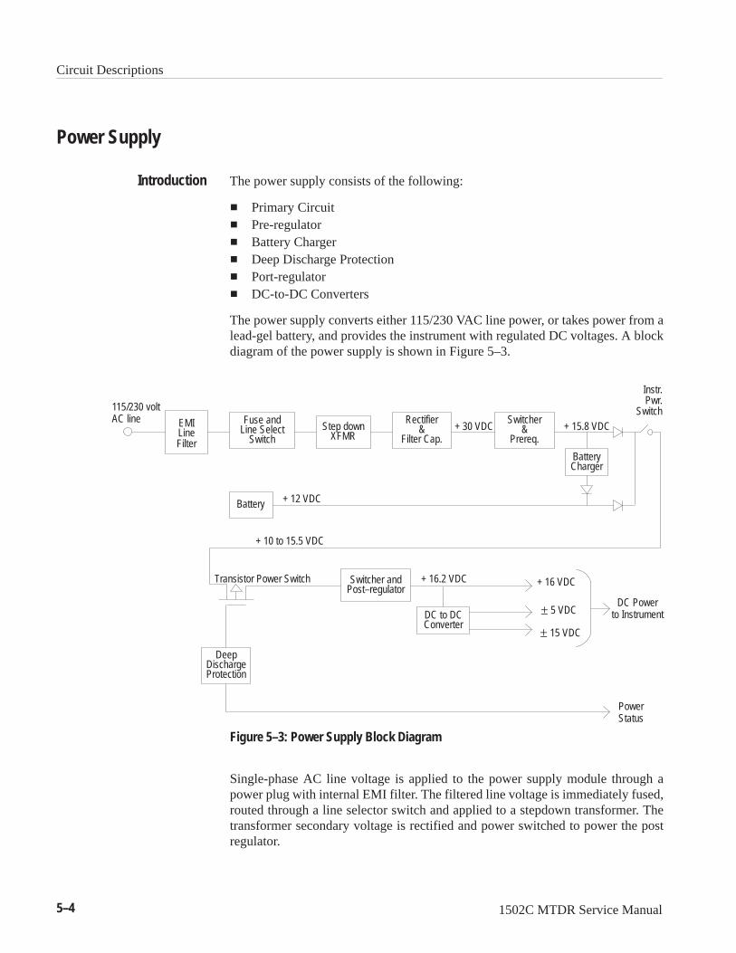
Circuit Descriptions
5–4 1502C MTDR Service Manual
Power Supply
The power supply consists of the following:
Primary Circuit Pre-regulator Battery Charger Deep Discharge Protection Port-regulator DC-to-DC Converters
The power supply converts either 115/230 VAC line power, or takes power from alead-gel battery, and provides the instrument with regulated DC voltages. A blockdiagram of the power supply is shown in Figure 5–3.
Fuse andLine Select
Switch
EMILineFilter
Step downXFMR
Rectifier&
Filter Cap.
Switcher&
Prereq.
BatteryCharger
Battery
Switcher andPost–regulator
DC to DCConverter
DeepDischargeProtection
115/230 voltAC line
+ 30 VDC + 15.8 VDC
Instr.Pwr.
Switch
+ 12 VDC
+ 10 to 15.5 VDC
Transistor Power Switch + 16.2 VDC + 16 VDC
± 5 VDC
± 15 VDC
DC Powerto Instrument
PowerStatus
Figure 5–3: Power Supply Block Diagram
Single-phase AC line voltage is applied to the power supply module through apower plug with internal EMI filter. The filtered line voltage is immediately fused,routed through a line selector switch and applied to a stepdown transformer. Thetransformer secondary voltage is rectified and power switched to power the postregulator.
Introduction

Circuit Descriptions
1502C MTDR Service Manual 5–5
A switching pre-regulator reduces this voltage to +15.8 VDC and is used to powerthe battery charger. This voltage is also processed through a rectifier and powerswitch to power the post-regulator.
If a battery is installed, the battery charger operates as a current source to providea constant charging current. Voltage limiting circuits in the charger prevent batteryovercharge by reducing the charge current as the battery voltages approaches +12.5VDC.
The battery provides a terminal voltage of 10 to 12.5 VDC, with a nominal capacityof up to 2.0 Amp-Hours. It also is connected through a rectifier to the instrument’spower switch and post-regulator.
When the power switch is closed, an FET power transistor is momentarily turnedon by the deep discharge protection circuit. If the voltage to the post-regulator risesto +9.7 VDC or greater, the transistor switch remains on. If at any time, the voltagedrops below +9.7 VDC, the transistor turns off and the power switch must berecycled to restart the instrument. This operation prevents discharge of the batterybelow +10 VDC. Such a discharge could cause a reverse charge in a weak cell,resulting in permanent cell damage.
The post-regulator is a boost switching regulator that increases its input voltage toa constant +16.2 VDC output. This voltage is supplied directly to the processor forlarge loads, such as the display heater, electroluminescent backlight, and optionsport. The post-regulator also supplies a DC-to-DC converter that generates5 VDC and 15 VDC for use in the instrument.
Status signals indicating whether the instrument is running on AC line voltage orthe battery, and if the battery is approaching turn-off level, are supplied to theinstrument by the deep-discharge protection circuits.
The AC line power is received by the connector in the EMI filter (FL1). This filterprevents high frequency signals generated in the instrument from being conductedback to the AC power line. The line voltage is fused (F101) and switched (S201)to the primary step-down transformer (T201). Both the switch and the fuse can beaccessed from the outside of the instrument via covers on the rear of the cabinet.
The primary of T201 is wound in two identical sections. These sections areconnected by S201 (in parallel for 110 VAC operation or in series for 220 VACoperation). The secondary of T201 is connected by a short two-wire cable to thePower Supply Board. The MOV (R101), across one of T201’s primaries, protectsthe power supply if 220 VAC is applied while S2011 is in the 110 VAC position.Fuse F101 will open in this event.
The secondary voltage is full-wave rectified by CR1010 and filtered by capacitorC1010. The large value of this capacitor allows it to supply energy to the instrumentbetween half cycles of the line voltage.
Primary Circuit
Pre-Regulator
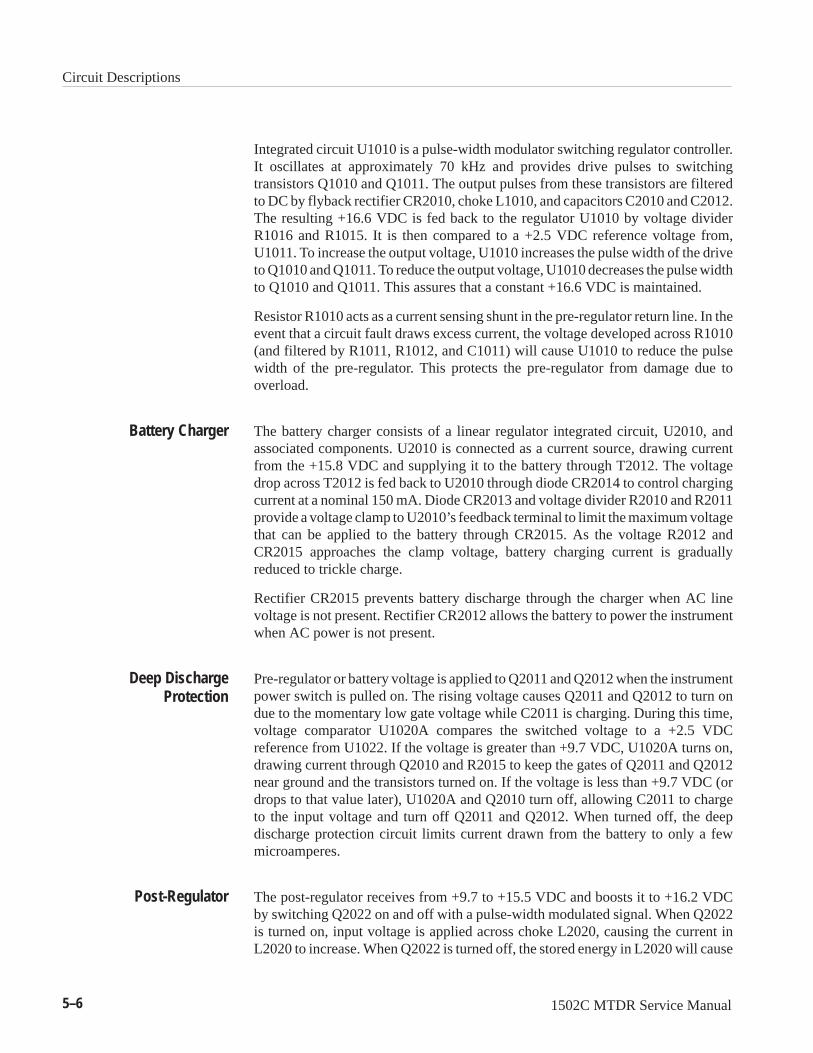
Circuit Descriptions
5–6 1502C MTDR Service Manual
Integrated circuit U1010 is a pulse-width modulator switching regulator controller.It oscillates at approximately 70 kHz and provides drive pulses to switchingtransistors Q1010 and Q1011. The output pulses from these transistors are filteredto DC by flyback rectifier CR2010, choke L1010, and capacitors C2010 and C2012.The resulting +16.6 VDC is fed back to the regulator U1010 by voltage dividerR1016 and R1015. It is then compared to a +2.5 VDC reference voltage from,U1011. To increase the output voltage, U1010 increases the pulse width of the driveto Q1010 and Q1011. To reduce the output voltage, U1010 decreases the pulse widthto Q1010 and Q1011. This assures that a constant +16.6 VDC is maintained.
Resistor R1010 acts as a current sensing shunt in the pre-regulator return line. In theevent that a circuit fault draws excess current, the voltage developed across R1010(and filtered by R1011, R1012, and C1011) will cause U1010 to reduce the pulsewidth of the pre-regulator. This protects the pre-regulator from damage due tooverload.
The battery charger consists of a linear regulator integrated circuit, U2010, andassociated components. U2010 is connected as a current source, drawing currentfrom the +15.8 VDC and supplying it to the battery through T2012. The voltagedrop across T2012 is fed back to U2010 through diode CR2014 to control chargingcurrent at a nominal 150 mA. Diode CR2013 and voltage divider R2010 and R2011provide a voltage clamp to U2010’s feedback terminal to limit the maximum voltagethat can be applied to the battery through CR2015. As the voltage R2012 andCR2015 approaches the clamp voltage, battery charging current is graduallyreduced to trickle charge.
Rectifier CR2015 prevents battery discharge through the charger when AC linevoltage is not present. Rectifier CR2012 allows the battery to power the instrumentwhen AC power is not present.
Pre-regulator or battery voltage is applied to Q2011 and Q2012 when the instrumentpower switch is pulled on. The rising voltage causes Q2011 and Q2012 to turn ondue to the momentary low gate voltage while C2011 is charging. During this time,voltage comparator U1020A compares the switched voltage to a +2.5 VDCreference from U1022. If the voltage is greater than +9.7 VDC, U1020A turns on,drawing current through Q2010 and R2015 to keep the gates of Q2011 and Q2012near ground and the transistors turned on. If the voltage is less than +9.7 VDC (ordrops to that value later), U1020A and Q2010 turn off, allowing C2011 to chargeto the input voltage and turn off Q2011 and Q2012. When turned off, the deepdischarge protection circuit limits current drawn from the battery to only a fewmicroamperes.
The post-regulator receives from +9.7 to +15.5 VDC and boosts it to +16.2 VDCby switching Q2022 on and off with a pulse-width modulated signal. When Q2022is turned on, input voltage is applied across choke L2020, causing the current inL2020 to increase. When Q2022 is turned off, the stored energy in L2020 will cause
Battery Charger
Deep DischargeProtection
Post-Regulator

Circuit Descriptions
1502C MTDR Service Manual 5–7
the current to continue flowing through CR2021 to filter capacitor C2025. Due toits stored energy, the voltage developed across L2020 adds to the input voltage,allowing C2025 to be charged to a voltage greater than the input.
The switching of Q2022 is controlled by pulse-width modulator U1023. Thepost-regulator output voltage is fed back to U1023 through R1025 and R1024 andcompared to the +2.5 VDC reference from U1022. Low output voltage causes widerpulses to be supplied to Q2022, storing more energy in L2020 during each pulse.This results in a higher output voltage. High output voltage, however, reduces pulsewidth and reverses the preceding process.
U1023 oscillates at approximately 80 kHz and supplies a synchronizing signal tothe pre-regulator at that frequency when the instrument is operating on AC power.This raises the pre-regulator frequency to the same 80 kHz. This synchronizationeliminates beat frequency interference between the two regulators.
The synchronizing signal from U1023 is also supplied to Q2021, where it isamplified to CMOS levels and buffered by gate U2030A. The signal is then usedto clock flip-flop U1024B to produce a 40 kHz square wave output at Q and Q. Thesesquare waves are buffered by other U2030 inverters and used to drive DC-to-DCtransistors Q2030 and Q2031.
Transistors Q2030 and Q2031 apply push-pull power to the primary of T1030 at40 kHz by switching the +16.2 VDC alternately between the primary windings. Theresulting transformer secondary voltages are rectified and filtered by CR1034,C1032, C1033, and C1034 to produce +15 VDC and –15 VDC. Other secondaryvoltages are rectified and filtered by CR1030, CR1031, CR1032, CR1033, C1030,C1031, and C1037 to produce +5 VDC and –5 VDC.
Diodes CR2031 and CR2030 rectify the primary voltage and clamp it to the voltagelevel that is across C2031. This prevents voltage transients caused by the rapidswitching of Q2030 and Q2031 and prevents the leakage inductance of T1030’sprimary from creating excessive voltage stress. R2030 provides a discharge pathfrom C2031. T1031 and C1036 provide additional filtering of the +16 VDC supply.
Processor System
The processor system consists of the following:
Microprocessor Address Decoding and Memory Interrupt Logic
The processor system provides control and calculation functions for the instrument.A block diagram of the processor system is shown in Figure 5–4 (next page).
DC-to-DC Converter
Introduction

Circuit Descriptions
5–8 1502C MTDR Service Manual
An eight-bit microprocessor, clocked at 5 MHz, provides the processing capabilityin a bus-organized system. Instructions are read from the program memory EPROMand executed by the microprocessor to accomplish essentially all instrumentfunctions. Random access memory is connected to the microprocessor through itsdata and address busses, allowing it to store and retrieve control, video, and displaydata, as required.
5 MHzCLOCK
MICROPROCESSOR
PROGRAMMEMORYEPROM
RANDOMACCESSMEMORY
ADDRESSDECODING
SELECT
DATA
AD
DR
ES
S
INTERRUPTLOGIC
INTERRUPT ANDSTATUS INPUTS
DATA SELECT ANDADDRESS SIGNALSTO CIRCUITS AND
OPTIONS PORT
Figure 5–4: Processor Block Diagram
The processor communicates with all other instrument circuits via the address, data,and select signals, and receives requests for service from those circuits via theinterrupt and status signals. Select signals are generated in address decoding circuitsunder control of the processor and used to read or write data from a circuit, or totrigger a circuit function. Interrupts from those circuits are combined in the interruptlogic to generate an interrupt request to the microprocessor. The processor respondsby reading a data word from this logic to determine the source of the interrupt, orstatus data, and then performs the required service routine.
The microprocessor, U1023, is a single chip processor using Z80 architectureconstructed in high-speed CMOS logic. Each data word, or byte, is eight bits wideand the microprocessor has a 16-bit address capability, allowing it to address up to65,536 memory locations. The processor’s 5 MHz clock is derived from a crystaloscillator in the timebase circuits.
When +5 VDC power is applied to C1030 and R1032, the rising voltagemomentarily applies a positive signal to the input of gate U1031B. The resulting
Microprocessor

Circuit Descriptions
1502C MTDR Service Manual 5–9
negative pulse at the gate output is supplied to U1023’s reset input, causing themicroprocessor to start at the beginning of its programmed routine each time poweris applied.
The 16-bit address space of Z80 processor U1023 is divided into five primary areas.They are:
Program Memory (EPROM) space RAM space Non-volatile RAM space Display RAM space Enable and Select Signal space
The program memory is stored in 64-kilobyte (kb) EPROM U2020, which isdivided into two 32–kb bank-switched halves. Both halves occupy locationsOOOOH to 7FFFH in the processor’s address space. The most significant addressbit on the EPROM, which determines which bank is addressed, is set by flip-flopU2030A. This bank-switching flip-flop can be toggled by the processor with twoselect lines, decoded in the enable and select signal address space. The select signalfor the EPROM is generated by combined address line A15 with the MREQ signalin U1045A. Whenever the processor addresses a location where A15 is not set, theprogram memory will be selected to place data on the bus.
The first RAM is eight-kilobyte memory U1021, selected by a signal generated bya 1-of-8 decoder, U1022. This decoder operates on the three most significant addressbits (A15, A14, A13) in combination with MREQ. Each of its decodes represents aselection of a particular 1/8 th of addressable locations. The first four decode signalsare not used because they are located in the program memory space. The fifth decodeis the select signal for the first RAM, occupying locations 8OOOH to 9FFFH.
The second RAM is also an 8-kb memory, U1020, made non-volatile by lithiumbattery BT1010 and non-volatile memory controller U1010. The select signal forthis RAM is generated similarly to that for the first RAM with the sixth 1/8 th decodeof U1022. This decode occupies AOOOH to BFFFH.
The display RAM is also an 8-kb memory, U1040, located in the display module.It is selected by the seventh decode of U1022. It occupies locations COOOH toDFFFH.
The remaining addressable space is used to generate enable, select, or triggersignals, which read, write, and control other circuits of the instrument. The eighth1/8 th decode signal of U1022 is used to enable four other 1-of-8 decoders: U2021,U2022, U2024, and U2026. These four decoders are further selected by the four
Address Decoding andMemory
Program Memory(EPROM)
RAM
Non-Volatile RAM Space
Display RAM Space
Enable and Select SignalSpace

Circuit Descriptions
5–10 1502C MTDR Service Manual
combinations of A12 and A11 and operate on A10, A9, and A8 to generate the enable,select, and trigger signals CS00 through CS31. These occupy the remaining addressspace, locations EOOOH to FFFFH.
An automatic wait state is inserted for all circuits selected by U2022. The wait stateis used by the processor to compensate for the slow access times of U2041, U2046,and U4020 on the Main Board; U2023 on the Front Panel Board; and U2040 on thedisplay module. The wait request is generated by U1041.
The select signals from U2024 are also modified through U1043B by a 200-ns pulse.This pulse is created from gates U1042B, U1031C, U2040C, and J-K flip-flopU2033A. This circuit creates a write pulse that ends prior to the completion of theprocessor bus cycle, thus meeting data hold time requirements for some selectedICs.
The most significant address bit on the EPROM is set or reset by bank-switchingflip-flop U2023A. Another control signal, heat disable, is generated by a similarflip-flop, U2023B. This is also toggled by two select lines.
The interrupt logic consists of an eight-bit tri-state buffer, U1032, and gates U1030and U1031D. Six interrupt requests signals are logically OR’d by U1030, theninverted by U1031D and applied to the microprocessor interrupt request input. Fiveof the interrupts are received from the video ADC, the digital timebase, a real-timecounter, the front panel control ADC, and from the Option Port connector. The sixthinterrupt input is unused.
The six interrupt requests and two power status signals are connected to pull-upresistors R1033 and the inputs of buffer U1032. When the microprocessor respondsto an interrupt request, it selects U1032, allowing the eight inputs to that device tobe placed on the data bus for reading.
The processor system outputs six control signals to the Driver/Sampler module.These signals are loaded from the data bus into latch U3010 by a select signal fromthe address decoder. These signals are used by the 1502C Driver/Sampler and theOption 06 adapter (if equipped).
Option Port Interface
The option port interface consists of the following:
Supply Controller Buffers Output Latch
The option port interface provides the connection between the processor system andexternal options. This port has a unique protocol that must be followed for proper
Additional Decoding
Interrupt Logic
Introduction

Circuit Descriptions
1502C MTDR Service Manual 5–11
and safe operation. Further information can be obtained by contacting yourTektronix customer service representative. A block diagram of the option portinterface is shown in Figure 5–5.
The processor system provides all the data and control for the interface. Data,Address, and Control lines are all buffered for increased drive. The power to theoption port is switchable to reduce power consumption, if necessary. The otheroutputs are available for control and protocol purposes.
SUPPLYCONTROLLER
BUFFERS
OUTPUTLATCH
POWER
DATA
ADDRESS
CONTROL
SWITCHED
POWER
Figure 5–5: Option Port Interface Block Diagram
The +16 VDC and +5 VDC power outputs to the option port are switched suppliescontrolled by the microprocessor system. CS14 and CS15 are used to set and clearflip-flop U1011B. This feeds comparators U1012A and U1012B. The positive (+)input to the comparators is set at 2.5 volts, so the CMOS flip-flop will drive thenegative (–) terminals above and below that voltage level. The comparators arepowered with a +16 VDC and a –12 VDC source to give a good output swing incontrolling the FET switches.
The output of U1012A controls the +16 VDC switch and is pulled up via a 20 kresistor, R2011. The output is also passed through two 100 k resistors, R2012 andR2013, to prevent the FETs from being over-driven. Two parallel FETs, Q2011 andQ2012, control the supply.
To reduce the instantaneous draw from the instrument supply when first turning theswitch on, capacitive feedback is used (C2016). This feedback slows the turn-ontime, allowing a capacitive load to be charged without affecting the instrumentsupply. A stabilizing 100 resistor, R2010, is also located in the feedback loop.
Supply Control

Circuit Descriptions
5–12 1502C MTDR Service Manual
NOTE. There are specified limits to this type of circuitry. Load specifications mustbe followed.
The arrangement of the +5 VDC switch is similar except that a 10 kkresistive divider is used to ensure the switch has a definite turn-on. A single FET,Q1010, controls the +5 VDC output.
Data lines to the option port pass through the bus transceiver, U2011. Address linesRD’ and WR’ are driven by U2012. CS22, from the processor system, enables thesedrivers with RD controlling the transceiver direction. U2012 outputs are pulled upby the switched +5 VDC supply, via R2015. The data lines are pulled down viaR2014.
WR’ is a modified write pulse 200 ns long, created to give a rising edge prior to thedisabling of the drivers. This pulse is created by flip-flop U2033A.
The output latch U1011A is controlled by A0 and A1, with select signal CS10. Theoutput of this latch is optionally used in the interface protocol.
Two more lines are used in the option port interface. IR4 is an interrupt signal thatis active low when creating processor interrupts. R-T TRIG is also available at theinterface. This is the trigger pulse generated in the analog timebase.
LabelJ2010
(on Main Board)Option Port
(D-Connector)
D0 3 2
D1 1 1
D2 24 25
D3 22 24
D4 20 23
D5 18 22
D6 16 21
D7 14 20
A0’ 12 19
A1’ 10 18
A2’ 8 17
A3’ 6 16
RD’ 7 4
WR’ 5 3
CS22 9 5
Buffers
Output Latch
Option Port WiringConfiguration

Circuit Descriptions
1502C MTDR Service Manual 5–13
LabelOption Port
(D-Connector)J2010
(on Main Board)
IA 11 6
IR4 13 7
R-T TRIG 2 14
SW+16 2523
1312
+16RTN 2119
1110
SW+5 17 9
+5RTN 415
158
Video Processor
The video processor system consists of the following:
Vertical Position DAC Summing Amplifier Video Amplifier Video DAC
The video processor receives sampled video from the driver/sampler and outputs adigitized video signal to the processor system data bus. A block diagram of the videoprocessor is shown in Figure 5–6.
Sampled Videofrom
Driver/Sampler
DATA
CONTROL
VIDEOADC
SUMMERAMPLIFIER
VERTICALPOSITION
DAC
DATABUS
CONTROL
INTERRUPTREQUEST
VIDEOAMPLIFIER
DATA
CONTROL
COMBINEDVIDEO
Figure 5–6: Video Processor Block Diagram
Vertical position information is loaded by the processor system into a DAC togenerate a DC signal. Sampled video is combined with this vertical position DCvoltage in a summing amplifier in order to allow vertical positioning of thedisplayed waveform.
Introduction

Circuit Descriptions
5–14 1502C MTDR Service Manual
The combined video and position signal is amplified by the user-selected gain in thevideo amplifier. Gain of the amplifier is set by the processor system via the data busand video amplifier select signal.
The amplified video is digitized by the video ADC upon receipt of a control signalfrom the processor system. The processor is notified by the ADC interrupt requestwhen the conversion has been completed. The processor then reads the value via thedata bus.
The vertical position DC voltage is generated by a digital-to-analog converterconsisting if U2046 and U3041. DAC integrated circuit U2046 receives a +2.5 VDCreference voltage from U3040 and multiplies it by a 14-bit digital value loaded fromthe data bus under control of the processor. The resulting current output of U2046is amplified by operational amplifier U3041 to a proportional voltage of zero to–2.5 VDC.
The summing amplifier consists of operational amplifier U8041; input resistorsR8044, R8046, and R8047; and a feedback resistor, R8045. Summation of the DACoutput through R8047 with the +2.5 VDC reference through R8046 causes thevertical position signal range to be enlarged and shifted to achieve an effectiveoutput of –2.5 VDC to +2.5 VDC.
Sampled video, through R8044, is summed with the vertical position signal at theinput node of U8041. Resistor T8045 determines the gain of U8041 and is paralleledwith C8040 to reduce high frequency gain for noise reduction. The sampled videoinput may be observed at TP9041.
Combined video from the summing amplifier is further amplified by a three-stageprogrammable video amplifier.
The first stage of this amplifier consists of amplifier U7040, voltage divider T8040through R8043, and analog multiplexer U8040. Voltage gains of 0, 16, 32, or 48 dBare achieved by switching U8040 to connect one of the four points from the resistivevoltage divider to the inverting input of U7040. This causes the amplifier gain tobe equal to the attenuation factor of the voltage divider point selected.
The second stage consists of amplifier U5040, voltage divider R6040 throughR6047, and analog multiplexer U6040. This stage operates similar to the first stageexcept eight voltage gains are provided from 0 to 14 dB in 2-dB steps.
The third stage consists of amplifier U3042, voltage divider T4040 through R4047,and analog multiplexer U4040. This stage operates similar to the first and secondstages except eight voltage gains are provided from 0 to 1.75 dB in 0.25-dB steps.
Gain of each of the three amplifier stages is controlled by the processor system byloading latch U2044 with the appropriate 8-bit word from the data bus. Digital word
Vertical Position DAC
Summing Amplifier
Video Amplifier

Circuit Descriptions
1502C MTDR Service Manual 5–15
00 (all 0s) selects 0 dB gain and word FF (all 1s) selects 63.75 dB gain. Allintervening values of 0.25 dB multiples are similarly chosen.
The output of the video amplifier is filtered by R2040 and C2043 for noisereduction, then sent to the analog-to-digital converter. The output may be observedat TP4040 (see Figure 5–7).
500mV
20nS
Figure 5–7: Video Processor Output
The output of the video amplifier is converted to its digital equivalent value by ADCdevice U2041. The conversion is done using successive approximation techniqueto compare the video voltage to the +2.5 VDC reference from U3040. The deviceis clocked by a 1.25 MHz clock derived from the timebase oscillator, and completesits 12-bit plus sign conversion in approximately 100 s.
Gate U2040 provides an OR function for the ADC start conversion trigger and readpulses from the processor system. Either pulse selects the ADC for control andconcurrent pulses select the trigger (WR input) or read (RD input) functions.
Upon completing a conversion, the processor system is notified by an interruptrequest (IR0) from U2041.
Timebase
The timebase circuits receive video sample time delay values in digital form fromthe processor system and generate precisely timed strobes to the driver/samplercircuits. Digital counters determine the delay in 50 ns multiples, and analog circuitsfurther define the delay to fractions of that period. A block diagram of the timebasecircuits is shown in Figure 5–8 (next page).
Video Analog-to-DigitalConverter
Introduction

Circuit Descriptions
5–16 1502C MTDR Service Manual
The digital portion of the timebase contains a clock generator that develops allfrequencies used in the instrument electronics.
TimebaseDAC
DATA
CONTROL
Analog
DriverStrobe
ComparatorVoltage
SAMPLER
CalDelay
CalRamp
PROCESSORCONTROL
GeneratorRamp
DelayCircuit
Time
DriverStobe PULSE
GENERATOR
RAMPTRIGGER
DRIVERTRIGGER
delay cal50 ns analog
DelayCounter
Fine
FormerPulse
TIMEBASEINTERRUPT
DelayCounter
Course
CounterPRTDATA
CONTROL
DATA
CONTROL
2.5 MHz
2.5 MHz
GeneratorClock SYSTEM
CLOCKS
20 MHz
5 MHz
2.5 MHz
1.25 MHz
625 KHz
20 MHz
20 MHz
Vref
DIGITALTIMEBASE
ANALOGTIMEBASE
Timebase
Correction
Figure 5–8: Timebase Block Diagram
A programmable digital counter, clocked at 2.5 MHz, is used to determine the PRT(pulse repetition time) of the driver/sampler test pulse. The 1502C is programmedwith a PRT of 350 s. The output of the PRT counter is used to trigger a delaycounter, also clocked at 2.5 MHz, to provide coarse (400-ns resolution) digital timedelay. The end of this time delay triggers a fine delay counter, which is clocked at20 MHz, providing 50-ns resolution to the sampler time delay. Both the coarse timedelay and the fine delay counters are programmed by the processor via the data bus.The end of the coarse delay is used to generate a timebase interrupt request to theprocessor to inform it that a sample is being taken and a timebase update is requiredfor the next sample.
The output of the fine delay counter is provided to the analog timebase circuits forfurther delay control to become the sampler trigger. The beginning of the coarsedelay counter period is detected by a pulse former, which generates a driver triggerfor the analog timebase.

Circuit Descriptions
1502C MTDR Service Manual 5–17
The analog timebase circuits receive the driver and sampler triggers and providestrobes to the driver/sampler. The driver trigger is delayed by an analog time delayand amplified by a driver circuit to provide the driver strobe.
The ramp trigger is used to start a linear voltage ramp generator. A voltagecomparator detects the time when this ramp reaches the programmed voltage of thetimebase DAC (digital-to-analog converter) and signals a driver to produce a strobefor the video sampler. The timebase DAC is programmed by the processor toprovide a voltage proportional to the portion of the 50-ns time delay period desired.
Timebase control by the processor system is shown in Figure 5–9. Each period ofthe pulse rate, the processor calculates a new 33-bit digital time delay value for thenext sample to be taken. The sixteen most significant bits of this value are loadedinto the coarse delay counter, causing it to count that number of 2.5 MHz clockperiods before starting the fine delay counter.
3 BITS16 BITS 14 BITS
MSB LSB33-BITDIGITAL TIMEDELAY VALUE
COURSEDELAY
COUNTER
FINEDELAY
COUNTER
ANALOGDELAY
2.5 MHzCLOCK
20 MHZCLOCK
STROBE TOSAMPLER
PRTPULSE
Figure 5–9: Timebase Control
The next three bits from the processor time delay value are loaded into the fine delaycounter. This counter starts at the end of the coarse delay, and counts the selectednumber of 20 MHz clock periods (o through 7) before triggering the analog delay.
The analog delay circuit receives the 14 least significant bits of the time delay word.A digital-to-analog conversion provides a proportional voltage, which is comparedto a linear voltage ramp to produce the programmed time delay (o to 50 ns).
The timing diagram in Figure 5–10 (next page) shows the combined effects of thethree time delays. The output of the PRT counter, waveform (a), begins the coarsedelay (b). The falling edge of this signal triggers the driver strobe (c), which causesa pulse to be applied to the cable test output.

Circuit Descriptions
5–18 1502C MTDR Service Manual
16 BIT
400 ns
3 bitprgmdelay
14 BITDACOUTPUT
PROGRAMMED DELAY
(a)
(b)
(c)
(d)
(e)
(f)
(g)
PRTCOUNTER
DELAYCOUNTER
DRIVERSTOBE
FINEDELAY
RAMPTRIGGER
RAMPGENERATOR
SAMPLERSTROBE
COURSE
COUNTER
[EXPANDED]
[EXPANDED]
Figure 5–10: Combined Effects of Time Delay
At the end of the coarse delay, the rising edge of this signal enables the fine delay(d), which produces a single ramp trigger pulse after the programmed delay. Thispulse is shown expanded in waveform (e). The ramp generator waveform (f), alsoshown expanded, has a linear voltage ramp beginning on the falling edge of thetrigger. This voltage is compared to the voltage from the timebase DAC, such thatwhen the ramp exceeds the DAC voltage, the sampler strobe (g) falls. This fallingedge is used as the sampler strobe for video sampling.
At the beginning of each sweep, the zero distance reference is calibrated to thefront-panel connector and the length of the analog ramp to 50 ns.
Zero distance reference is calibrated by setting the digital and analog timebase forzero delay. Then the processor adjusts the driver delay so as to sample at the 10%point of the pulse. The ramp is calibrated by removing 50 ns of delay (one 50-nsclock cycle) from the sample trigger and then reinserting it with the analog delay.The processor adjusts the reference for the timebase DAC so as to sample at theprevious level. This matches the analog delay to the 50-ns period of the clock.

Circuit Descriptions
1502C MTDR Service Manual 5–19
50 n
s
STA
RT
PU
LSE
VA
R. D
ELA
Y R
AM
PT
O S
ET
DE
LAY
ZE
RO
CO
MP
AR
AT
OR
LE
VE
L S
ET
SO
SA
MP
LE T
AK
EN
AT
10%
PO
INT
ON
OU
TP
UT
PU
LSE
PU
LSE
OU
T
10%
LE
VE
L
CO
MP
AR
AT
OR
OU
TP
UT
DE
LAY
ZE
RO
SE
T
50 n
s R
AM
P S
ET
FIX
ED
CIR
CU
ITD
ELA
YS
50 n
s R
AM
P S
TAR
T
0V =
0 D
ELA
Y
50 n
s D
ELA
Y
CO
MP
AR
AT
OR
LE
VE
LS
ET
TO
SA
MP
LEP
ULS
E A
T 1
0% P
OIN
TO
N O
UT
PU
T P
ULS
E
0V C
OM
PA
RA
TO
R L
EV
EL
= 0
DE
LAY
4V =
50n
s D
ELA
Y
∼∼
20 M
Hz
CLK
TP
2031
TR
IG T
O
TR
IG T
O
SA
MP
LE T
RIG
PU
LSE
TR
IGD
IGIT
AL
DE
LAY
PU
LSE
GE
N.
TP
9011
SA
MP
LER
TP
7010
TP
2030
Figure 5–11: Calibration of Delay Zero and 50-ns Analog Delay

Circuit Descriptions
5–20 1502C MTDR Service Manual
All digital clocks from the instrument are derived from a 20 MHz crystal oscillator,U2031. Flip-flops U2042A and U2042B divide the clock frequency to 10 MHz and5 MHz respectively. The 5 MHz output is provided to the microprocessor and toTP2041.
Gate U2034B decodes one of the four states if U2042 and provides a 5 MHz pulseto U2033B. Flip-flop U2033B is clocked by the 20 MHz clock and divides the 5MHz signals to 2.5 MHz synchronously with the 20 MHz. The 2.5 MHz clock isfurther divided to 1.25 MHz by U2025A and 625 kHz by U2025B.
The PRT, coarse delay, and real-time counters are contained in a triple, 16-bit,programmable counter device, U2030. The PRT and coarse delay counters areclocked at the 2.5 MHz rate. The output of the PRT counter, pin 10 of U2030, isapplied to the trigger input of the coarse delay counter as a start-count signal. Thenegative-going pulse from the coarse delay counter, pin 13 of U2030, is input to atwo-stage shift register, U2032C and U2032D. This shift register is also clocked at2.5 MHz and serves to delay the signal and reduce its skew relative to the 20 MHzclock. The Q (inverted output) of U2032C is a positive-going pulse that is suppliedto a three-stage shift register, U2036B, U2036D, and U2036A, which is clocked at20 MHz from inverter U2034A. The leading edge of the pulse is decoded by NANDgate U2045B, which also ANDs the signal with the 20 MHz clock from inverterU2045A. The resulting driver trigger pulse is a negative-going pulse of nominally25 ns width. The falling edge of this pulse is determined by the edge of the 20 MHzinput to gate U2045B and is used as the driver trigger.
The coarse delay pulse from shift register U2032D and U2032C us decoded by NORgate U2034C to detect the pulse rising edge (end of the negative pulse). Theresulting positive pulse is 400 ns wide (one cycle of the 2.5 MHz clock). This pulseis shifted through flip-flop U2036C to synchronize it with the 20 MHz clock andapplied to the count enable input of U2037, a four-bit programmable counter.
Counter U2037 will have been preset to a count of 8 through 15 by the processorthrough latch U2043 with CS11. While the count enable pulse is present, it willcount exactly eight times at the 20 MHz rate, thus passing through count 15 after0 through 7 clock pulses. The terminal count (TC) output of U2037 is a decode ofcount 15. Thus this signal creates the fine delay pulse after the programmed delay.This positive-going pulse is gated with the 20 MHz clock by NAND gate U2045Cto provide a 25 ns negative-going pulse for the ramp trigger. Ramp timing is derivedfrom the trigger falling edge.
The end of the coarse delay, detected by gate U2034C, is used to clock U2027A,which generates an interrupt request to inform the processor that a sample is beingtaken. An acknowledge pulse, CS16, from the address decoder resets this flip-flop.
The logic level driver trigger from the digital timebase is first amplified by transistorstage Q9021. The trigger is capacitively coupled through C8022 and R9027 to shiftit to analog levels. The collector of Q9021 is clamped to –0.5 VDC between pulsesby CR8020 and rises to +6 VDC peak during the 25 ns pulse. This signal is applied
Digital Timebase
Analog Timebase

Circuit Descriptions
1502C MTDR Service Manual 5–21
to C8021 through R8025 to generate an exponentially rising pulse of about 4 VDCpeak during the pulse width.
Dual transistor Q8020 is a differential amplifier that is used as a voltage comparatorto detect when the pulse on C8021 has reached the DC voltage level set throughU4021B and R8023 by the zero-distance calibration circuit. This DC voltage level,from zero to 4 VDC, allows setting the time when the voltage comparator switches(a range of about 20 ns). Dual transistor Q9020 is connected as a current source,providing a constant 2-mA bias to the emitters of Q8020. Between pulses, thiscurrent flows through Q8020B. When the exponential pulse reaches the adjustablevoltage level, the current is rapidly transferred to Q8020A, causing a negative-goingpulse at R8020. This pulse is coupled to the output stage, Q9010, through C9020and R9020. Transistor Q9010 is biased to 0.5 mA between pulses to obtain fastturn-on, and provides a positive-going 5 VDC pulse to U8010B and U8010C.Flip-flop U7010A is set or reset by the processor to steer the pulse either to theoption port or the driver. The negative-going pulse from gate U8010B or U8010Cis logically OR’d by U8010A, then applied to C9010 and R9010. This pulse is fedback to the input of the gates U8010B and U8010C through CR9010 to obtain aone-shot action, which stretches the driver strobe pulse width to 5 s. The driverstrobe is made available at TP9011.
The ramp trigger pulse from the digital timebase is AC-coupled by C3040 andR3041 to Q4040. Diode CR3031 allows the negative-going pulse to pass directly,while R3040 limits the input current sue to the re-charging of C3040 betweenpulses. The output of Q4040 is held at ground by L5030 between pulses and risesto 6 VDC during the pulse. Choke L5030 is center tapped to provide an equalnegative-going pulse at its undriven end. This pulse is fed through C5033 andR4032 to the emitter of Q4031 to obtain positive feedback to Q4040. This forms aone-shot circuit with the pulse width determined by C5033 and R4032. The 25 nsramp trigger pulse is thus stretched to about 80 ns at L5030.
Dual transistor Q5032 operates as a current source, providing a constant 5-mAcurrent, which is used to charge C5032 to create a linear voltage ramp. Betweenramp trigger pulses, this current is conducted through CR4032 and L5030 to ground,creating a voltage of 0.5 VDC on C5032. The positive one-shot pulse from Q4040turns off CR4032 and directs the charging current to C5032. The negative-goingpulse from L5030 is connected to C5032 through CR5030 to provide a cancellingeffect for the positive pulse being coupled through the capacitance of CR4032.
The linear rising voltage pulse from C5032 is buffered by source-follower Q5031and emitter-follower Q5030 to provide a low output impedance and prevent loadingthe ramp. Transistor Q7030 provides a constant 2-mA bias current to junction FETQ5031.
The ramp voltage is AC-coupled to voltage comparator Q7021 by C7030 to removethe DC offset voltage developed in the preceding circuits. A small negative DCvoltage of approximately –200 mV is added by voltage divider R7032 and R7025to hold the voltage comparator off between pulses.

Circuit Descriptions
5–22 1502C MTDR Service Manual
Voltage comparator Q7021 is biased at 2 mA by dual transistor Q5020. During thelinearly rising ramp voltage, it compares the ramp to a programmed DC samplereference voltage produced by the timebase DAC circuit. When the ramp reachesthe sample reference value, Q7021A rapidly turns on to produce a negative-goingsignal across R7024. This pulse is coupled through C7022 and R7021 to turn onQ6020, providing a positive pulse to the base of Q7020. The negative-going samplerstrobe coming from Q7020 is supplied to the sampler and to TP7010.
Timebase DAC U4020 and amplifier U5010 inverts and multiplies VREF by the14-bit digital word loaded by the processor. It is filtered for noise by R7026 andC5023 and connected to comparator Q7021 through R7027 to set the analog delay(0 to 50 ns).
To calibrate the analog delay to 50 ns, the processor sets IR2 (IR2 high) and loadsa new 12-bit word in latches U3021 and U3022 (max 1-bit change per sweep) withchip selects CS11 and CS12. DAC U3023 multiplies the reference current (1 mAset by R3020) by the digital word from the latches. The DAC output current andthe current from the last two LSBs (which comes from the latches through R3031,R3033, R3039, and R4020) are summed by U4021A and forced through R4021.This develops a correction voltage at TP4020 of 5 VDC and a sensitivity of2.5 mV per bit (the currents from the LSBs have been complimented by theprocessor to correct their phase). The DAC circuit is designed to nominally run athalf of full dynamic range (2048/4096) of 2 mA, that generate 1 mA of current atthe summing node. That current is balanced out by 1 mA of current from R4020,giving a nominal output of zero volts at TP4020 and TP4021.
U5020, R5020, R5021, and C5021 scale the correction signal (up to 5 VDC) atTP4020 to 0.4 VDC at VREF of U4020. Resistors R5023 and R5022 furnish acurrent to offset VREF to a –4 VDC 0.4 VDC (equivalent to 5 ns) correctionsignal to the 50 ns analog delay.
To calibrate, the zero-distance delay (IR2) is set low, and through R3037 andCR3030, turns on Q3030, whose collector (through R3036 and R3035) raises thecathode of CR4030 to +6 VDC. This allows R4023 to turn on Q4030. CapacitorC4022, through R4030 and Q4030, is charged to the new corrected level at TP4020that was asked for by the processor. The correction voltage on C4022 from bufferamplifier U4021B is scaled by voltage divider R8023, R8022, and R8021 from arange of 5 VDC to a range of zero to 3.5 VDC. This voltage is applied to the baseof comparator Q8020B, which provides 10 ns of zero-distance delay adjustment.Components C3048, R3042, R2032, C3047, R2034, and C8024 are used to reducejitter and cross-coupling between circuits.

Circuit Descriptions
1502C MTDR Service Manual 5–23
Driver/Sampler
The front-end consists of:
Hybrid Sampler/Step Generator Second Sampler
First Sampler Bridge Bias Generator
Trigger Pulse Shapers
Power Supply Conditioning
The function of this board is to generate the step test signal and to sample and holdthe reflections from the cable under test. A block diagram of these circuits is shownin Figure 5–12 (next page).
Most of the primary active circuitry is located within the hybrid. The balance of theDriver/Sampler Board is dedicated to interfacing with the rest of the instrument.
The step generator is triggered by a negative pulse from the Main Board. One of thetrigger pulse shapers stretches this to 25 s to set the length of the output step. The0.6 V adjustable power source sets the “on” voltage for the output step.
The sampler is also triggered by a negative pulse from the Main Board. Inside thehybrid, this trigger causes the strobe generator to apply 50-ps pulses to turn on thebridge, capturing a portion of the input waveform. This sample is stored outside thehybrid in the second sampler to reduce droop rate. The stored signal goes two places:back to the Main Board as the video output, and to the bridge bias circuit, whichholds the sampling bridge off between samples.
The video signal from the hybrid is sent to the second sampler. The second samplerreduces the droop rate to about 1 LSB/ms. This is accomplished by buffering thesignal through U2050B and storing it in C2053 via the FET switch, Q1060. The FETis strobed by the one-shot U3030B for 5 s after the sample is taken. The voltagestored on C2053 is buffered by op-amp U2050A, then inverted and amplified byU1050A. The strobe signal for the FET can be observed at TP2060, and the invertedvideo output at TP1060. The signal from the second sampler buffer, U2050A, is alsofed to the bridge bias amp, U1070, via R1060.
Introduction
Second Sampler

Circuit Descriptions
5–24 1502C MTDR Service Manual
Regulator± 12V ± 12V± 15V
On boardsupply
25 µsOne Shot
5 µs
One Shot
Step trigger
InvertedVideo Out
–1.6
Sample trigger
0.6 VAdjustable
source
StepGenerator
Samplerstrobe
generator
2ndSampler
Hybrid
Samplingbridge
+B
–B
Bridgebias
Frontpanelcable
connector
Figure 5–12: Driver/Sampler Block Diagram
The bridge bias for the first sampler is set by U1070. With a zero voltage inputsignal, the circuit holds 2.0 V on the bridge inputs. As the input signal moves, the4 V window also moves to stay centered around it. This centering is accomplishedby feeding part of the output of U2050A into the bridge bias circuit. The outputs ofthe bridge bias circuit are available on TP1020 and TP1021.
There a\re two incoming triggers: the sample and the step. Both require modificationbefore they are usable by the hybrid. The sample trigger is a 30-to-50-ns negativeTTL signal. This pulse is buffered by Q2030, then coupled to the hybrid throughT1020. This provides a differential drive that can have common-mode voltage onit. The sampler pulse is also stretched to 5 s by U3030B to strobe the secondsampler. The step trigger, GEN TRIG, is a 3-to-5-s negative TTL signal, stretchedto the proper 25 s pulse length by U3030A. CR3020 and CR3021 provide a logicOR of the incoming signal and the output of the one-shot. This prevents theintroduction of jitter on the trigger signal. The OR output can be observed atTP3020.
There are seven power supplies for the hybrid: 5 VS, 5 VP, 12 V, and +0.6 V.The 5 V supplies come on board as 5 V, so they require no regulation, but aremerely filtered before being used by the hybrid and the board. The 12 V suppliesenter the board as 15 V, so the necessary filtering and regulation is accomplishedby U3070 and associated circuitry. The +0.6 V supply is used by the hybrid to set
Bridge Bias
Trigger Pulse Shapers
Power Supply Conditioner

Circuit Descriptions
1502C MTDR Service Manual 5–25
the output step height. It is referenced to the +5 V supply and controlled by U1050Band Q1030.
The +0.6 V supply is adjustable via R1042 to allow the offset of the step generatorto be zeroed out. CR1040 temperature compensates the +0.6 V supply againstvariations in the hybrid. The test points for these supplies are as follows:
+5 V TP1083–5 V TP1084
+12 V TP1080–12 V TP1081
+0.6 V TP1030Ground TP1082
Front Panel
The Front Panel Board consists of the following circuits for these controls:
Push Button Switches and Latches Rotary Binary Switches Resistive Shaft Encoders Analog-to-Digital Converter for Shaft Encoders
The Front Panel Board consists of the following circuits for the display module:
Electroluminescent Backlight Switch and Power Supply Display Heater Circuitry Display Drive Voltage (Contrast) Temperature Compensation
The Front Panel Board contains most of the instrument control as well as somecircuitry for the display module. A block diagram of the Front Panel Board is shownin Figure 5–13 (next page).
The push button switches are normally open momentary switches When depressed,these switches tie the inputs of NOR gate latches U3021, U3022, and U3023 to +5VDC, setting the latches. The latches are reset by control signal ADCRD. Theprocessor updates the instrument configuration by periodically reading the state ofthe latches through multiplexers U2024, U3025, and U3031.
These switches control:
MENU VIEW INPUT VIEW STORE VIEW DIFF STORE
Introduction
Push Button Switches andLatches
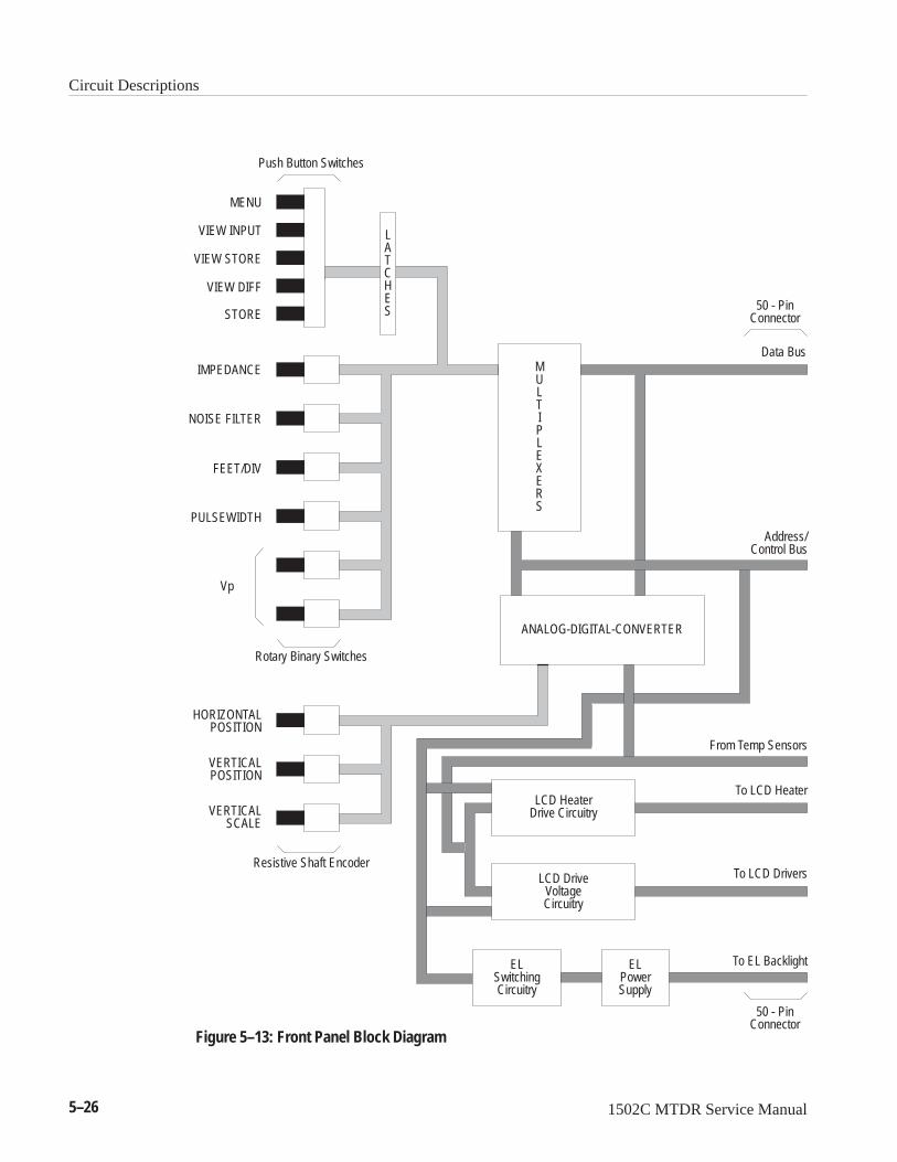
Circuit Descriptions
5–26 1502C MTDR Service Manual
Push Button Switches
Rotary Binary Switches
Resistive Shaft Encoder
MENU
VIEW INPUT
VIEW STORE
VIEW DIFF
STORE
IMPEDANCE
NOISE FILTER
FEET/DIV
PULSEWIDTH
Vp
HORIZONTALPOSITION
VERTICALPOSITION
VERTICALSCALE
50 - PinConnector
Data Bus
Address/Control Bus
From Temp Sensors
To LCD Heater
To LCD Drivers
To EL Backlight
50 - PinConnector
LCD HeaterDrive Circuitry
LCD DriveVoltageCircuitry
ELSwitchingCircuitry
ELPowerSupply
ANALOG-DIGITAL-CONVERTER
MULTIPLEXERS
LATCHES
Figure 5–13: Front Panel Block Diagram

Circuit Descriptions
1502C MTDR Service Manual 5–27
The rotary binary switches provide a 4-bit binary value, indicating their position.The outputs are tied to the inputs of the multiplexers. The position of the rotaryswitches control the following functions:
FILTERING, SET REF, SET DELTA HORIZONTAL GAIN (DIST/DIV) VP COARSE VP FINE
The switch multiplexers are U2024, U2025, U3025, and U3031. These dualfour-channel multiplexers multiplex the switch settings of the push button androtary switches onto the data bus. The control signal MUXCS, in conjunction withA2, selects the multiplexers while A0 and A1 determine which switch bank is placedon the data bus.
The resistive shaft encoders R1022, R2024, and R3020 are dual-concentric, 360°rotation potentiometers, with the wipers set 180° out of phase with respect to eachother. The wipers are tied to the analog-to-digital converter inputs of ADC U2023.The three resistive shaft encoders control the following functions:
VERTICAL GAIN VERTICAL POSITION HORIZONTAL POSITION (Cursor)
The ADC, U2023, is an eight-channel analog-to-digital converter. It converts thevoltages on the wipers of the resistive shaft encoders to a digital value, dependingon the position of the encoders. It also converts the voltage on the display thermistor(TSENSE) and the chart recorder thermistor divider circuits into digital valuesrepresenting the corresponding temperatures. The temperature data is used by theprocessor to compensate the LCD drive voltage and chart recorder print parametersfor variations in temperature.
The control signal TRIG ADC is used to start a conversion; ADC RD reads thevalue; and A0, A1, and A2 select one of the eight channels for conversion. Controlsignal EOC notifies the processor of a conversion completion, via the IR3 line.
The EL (electroluminescent) backlight is switched by software. Control signalLIGHTCS, with RD or WR, sets or resets (respectively) NOR latch U3020. Theoutput of the latch is applied to the + side of comparator U2020B; the – side is heldat 2.5 VDC. When the output of the latch is high, the comparator output is +16 VDC,which turns off the gate of P-channel FET Q1030, turning off power to the EL powersupply, PS2030. When the output is low, the comparator output is 0V, which turnson the FET, turning on the power to the EL power supply. R1031, C3030, and C3031serve to filter noise introduced to the +16 VDC supply by the EL power supply.
Rotary Binary Switches
Switch Multiplexers
Resistive Shaft Encoders
Analog-to-DigitalConverter
ElectroluminescentBacklight Switch and
Power Supply

Circuit Descriptions
5–28 1502C MTDR Service Manual
The display heater circuitry regulates the application of power to the display heater(see Indium Tin Oxide Heater later in this chapter for more information). When thedisplay thermistor divider senses the display temperature has dropped below+10° C, the heater can be turned on if the control signal HEAT ENABLE is notasserted. For reasons of power economy, the chart recorder and display heater arenot allowed to operate concurrently. The processor does this by asserting HEATENABLE while making a chart recording. When HEAT ENABLE is low,N–channel FET Q2020 is off, making the voltage on the + side of the comparator,U2020A, approximately +5 VDC. This will allow the + side (chart recorder) toalways be greater than the – side (display thermistor divider voltage). The outputof the comparator will be +16 VDC, which turns off P-channel FET Q1020. Thisturns off the power to the display heater.
When HEAT DISABLE is high, Q2020 will turn on and the voltage on the + sideof the comparator will be approximately 2.5 volts. When the display thermistordivider voltage (– side) is above 2.5 volts (about +10° C), the comparator output willbe 0 V, which will turn on Q1020. This will turn on the heater. As the temperaturerises above +10° C, the thermistor divider voltage will be less than 2.5 V and Q1020will turn off, shutting off power to the heater.
The LCD drive voltage compensation circuitry adjusts the drive voltage (contrast)to assure a constant display contrast within the operating temperature range of theinstrument. The display thermistor is attached to the LCD and forms the sensor inthe display thermistor divider circuit. Its output is a voltage related to the displaytemperature. This voltage is read by the processor through the analog-to-digitalconverter, U2023. The processor uses this voltage value to determine a drivevoltage. This is sent to digital-to-analog converter U2021 via the data bus. Theoutput of the DAC is amplified to op-amp U2010A and applied as the LCD drivevoltage. As the temperature of the display (thermistor divider voltage) changes, theprocessor modifies the drive voltage via the DAC. In this manner, the drive voltageis compensated due to variations in display temperature. Trimmer potentiometerR1011 is used to offset the drive voltage produced by U2010A to compensate forvariations in display cells and thermistors.
Display Module
The display module consists of the following:
LCD Cell Row Driver/Controller Board and Column Driver Board Electroluminescent Backlight Indium Tin Oxide (ITO) Heater Mechanical frame, which supports the above subassemblies
Display Heater Circuitry
Display TemperatureCompensation
Introduction

Circuit Descriptions
1502C MTDR Service Manual 5–29
The display module function is to take bit pattern data generated by the instrumentinternal electronics and display it on the LCD. A block diagram of the displaymodule is shown in Figure 5–14.
DATA/CONTROL
DISPLAYMEMORY
4K X 8
ADDR
ADDR
DATAC
ON
TR
OLL
ER
40-P
IN C
ON
NE
CT
OR
ROWDRIVER
ÄÄÄÄÄÄÄÄÄÄÄÄÄÄÄÄ
ÄÄÄÄÄÄÄÄÄÄÄÄÄÄÄÄ
column driver [4]
column driver [4]
upper
lower
SBE CELL128 X 256
boar
d-to
-boa
rdel
asto
mer
flex
cabl
e
columnelastomer
columnelastomer
64 64 64 64
64 64 64 64
64
64
ROW DRIVER/CONTROLLER BOARD COLUMN DRIVER BOARD
DATA/CONTROL
Figure 5–14: Display Module Block Diagram
The LCD cell is the “video screen” that displays information generated by theprocessor. The processor updates the display memory periodically with a newpicture and the display memory holds this bit pattern data. This data is received bythe display controller and sent to the drivers along with some control and timingsignals that provide operating information to the drivers. The row and columndrivers are attached electrically to the LCD cell through elastomeric connectors anda flex cable. These drivers place signal voltages on the electrode matrix in the LCDcell and thus generate the video display.
There are other circuits contained in the display module. An indium tin oxide (ITO)heater warms the display during cold temperatures. A temperature sensor attachedto the display provides display temperature data to the heater and drive voltagecircuitry (see Front Panel text in this chapter). An electroluminescent backlightprovides illumination in low light conditions.
The LCD cell provided in the 1502C uses an advanced technology known asSuperbirefringent Effect (SBE) to obtain greatly improved contrast and viewing
LCD Cell

Circuit Descriptions
5–30 1502C MTDR Service Manual
angle over conventional LCD cells. The function of the LCD module is to receivebit pattern data from the CPU and display it.
First, the processor generates a 4k X 8-bit pattern image in its own memory. It thenwrites this bit pattern, via the data bus, to the display memory, U1040, in the formof a block transfer. The bit pattern is mapped in the display memory and later on theLCD cell.
Second, the LCD controller, U2040, reads the bit pattern from the display RAM,formats it, and sends it to the column drivers.
Last, the column drivers and the row drivers generate select and non-select voltagesbased on the timing, control, and data signals received from the controller. Thesevoltages are applied to the LCD cell matrix, turning off and on pixels that match thebit pattern in the display memory. The pattern of pixels form the image on thedisplay.
The cell is physically composed of two planes of glass, two polarizers, a matrix oftransparent electrodes, and a filling of liquid crystal material. A plating of indiumtin oxide on the back plane of glass is used as a heater, but is not used in the displayprocess.
Electrically, the cell is a 128 X 256 pixel display, each pixel being an intersectionof a row and a column. These intersections are like small capacitors. When anon-select voltage (about 1.5 VRMS) is applied to a row and a column, theirintersection is turned off (see Figure 5–15). That is, light is allowed to pass throughthe display and reflect back from the transflector, creating an “off” pixel. A selectvoltage (about 1.7 VRMS) turns the intersection on. That is, the light is not allowedto pass through the crystalline material and is, therefore, not reflected back from thetransflector, creating an “on” pixel.
RO
W 128
RO
W 127
RO
W 65
RO
W 64
RO
W 2
RO
W 1
COLUMN 1COLUMN 2
COLUMN 255COLUMN 256
LOWER HALFSCREEN
UPPER HALFSCREEN
Figure 5–15: SBE Cell

Circuit Descriptions
1502C MTDR Service Manual 5–31
There is one row driver, located on the Row Driver/Controller Board. There are eightcolumn drivers, located on the Column Driver Board. The row and column driversreceive control, timing, and data signals from the controller and translate them toproperly timed voltages that are placed on the pixel matrix. The voltages are placedon the matrix by the flex cable for the rows and by the elastomers for the columns.
ROW 64 - ROW 128 ROW 1 - ROW 65
GND
N.C.
LATCH
64 - BIT SHIFT REGISTER
64 - BIT LATCH
64 - BIT LEVEL SHIFTER
LP
ST
Vccd
V5
V2
+5
FR
Figure 5–16: Row Driver Block Diagram
The function of the row driver is to sequentially address each of the rows of thedisplay. The on or off state of the pixels on the addressed row is then determined bythe voltages on the columns. The row driver addresses each line, one after another,completing the scanning at the refresh rate of 125 Hz.
The column driver is similar to the row driver except bit pattern data is level-shiftedrather than the start pulse. The column drivers provide select and non-select voltagesto the column electrodes according to the bit pattern data. The presence of selector non-select voltages on the columns, in conjunction with the currently selectedrow pair determine which pixels are on or off on that row pair. The column driversregulate the select and non-select voltages as the row drivers select rows. The resultis a bit pattern displayed on the screen that represents a waveform.
Row and Column Drivers

Circuit Descriptions
5–32 1502C MTDR Service Manual
Gnd
Vlcd V
4V
3+
5
Eclk
Ein
Eout
Xscl
D3
D2
D1
D0
LpFr
Column X 64
Column X Seg 63
64 - Bit Level S
hifter
64 - Bit Latch
16 position4-bit w
ideshift register
DQQ
Figure 5–17: Column Driver Block Diagram
The row driver is an 80-pin flat pack located on the Row Driver/Controller Board.It is composed of a 64-bit shift register, U2020, a 64-bit latch, and a 64-bit levelshifter. The row driver has the following relevant inputs:
ST <start pulse>: Input to the shift register <Din on SED 1190> LP <latch pulse = LATCH>: Falling-edge triggered, this shifts data in the shift
register and latches contents of the shift register into the latch <Y SCL onSED 1190>
FR <frame signal>: Defines the select and non-select voltages.
The relevant outputs:
Row 1 through 64 are paralleled outputs driving both sides of the display. One setof outputs drive rows 1 through 64 and the other set drive rows 65 through 128 onthe LCD.
Supply Voltages include the following:
+5 VDC supply voltage for logic and select drive voltage V2 non-select drive voltage V5 non-select drive voltage VLCD select voltage GND return for +5 VDC.
Row Driver
Circuit Descriptions
1502C MTDR Service Manual 5–33
1 Frame = 8 ms
63 64 1 2 3 63 64
+5
V2
Scanning select pulse
V5VLDC
+5
V2
V5VLDC
V5VLDC
+5
V2
LPX–LP
Figure 5–18: Row Timing Diagram
To perform its function, the row driver receives a start pulse at the beginning of aframe. LP shifts this start pulse into the shift register. The contents are thentransferred to the latch. The level shifter shifts the logical 1s and 0s in the latch intoselect and non-select voltages according to FR (see table at top of next page).
Circuit Descriptions
5–34 1502C MTDR Service Manual
FR Bit X in Latch Row X Output0 0 V5 non-select
0 1 +5 VDC select
1 0 V2 non-select
1 1 VLCD select
ST, LP, and FR are sent by the controller in such a way that a scanning select voltageis applied sequentially to the rows, with the polarity of the select voltage alternatingwith FR, every frame. The alteration is required to place an AC voltage on the pixels.
A column driver is composed of several blocks: 16-position, 4-bit wide shiftregister; 64-bit latch; 64-bit level shifter; and an enable flip-flop.
A column driver has the following relevant inputs:
D3–D0 <data MSB to data LSB>: Bit pattern data for data formatted and sentby the controller
XSCL <column (X) shift clock>: Shifts D3–D0 in parallel groups of four bits LP <latch pulse>: Latches data in shift register into 64-bit latch FR <frame signal>: Defines select and non-select voltages EIN <enable in>: Input to the enable flip-flop ECLK <enable clock>: Clocks EIN into the enable flip-flop.
The relevant outputs:
Columns 1 to 64: These are the 64 outputs from the level shifter.
NOTE. The manufacturer’s pinout of the outputs are numbered in order of shift (seg63 – seg 0). The nomenclature herein refers to the outputs in column order.Therefore, seg 63 corresponds to Column 1 and seg 0 corresponds to Column 64.
EOUT: Output from the enable flip-flop.
Supply Voltages include the following:
+5 VDC supply voltage for logic and select drive voltage V3 non-select voltage V4 non-select voltage VLCD select voltage GND return for +5 VDC
Column Driver

Circuit Descriptions
1502C MTDR Service Manual 5–35
One Line
Extra
1 116 64
64-LP
(Non Select Bits)
Vlcd (Select Bits)
One Frame
+5V (Select Bits)
V4
(Non Select Bits)
11 1 116 16 16
V3
First ColumnDriver Pair
Enable
Second ColumnDriver Pair
Enable
Third ColumnDriver Pair
Enable
Forth ColumnDriver Pair
Enable
Figure 5–19: Column Timing Diagram
To perform its function, the column driver shift registers are filled with data byreceiving data, XSCL, ECLK, and EIN from the controller. LP then latches thecontents of the shift registers into the latches. The level shifter translates the logical1s and 0s in the latch into select and non-select voltages according to FR (see table,next page).
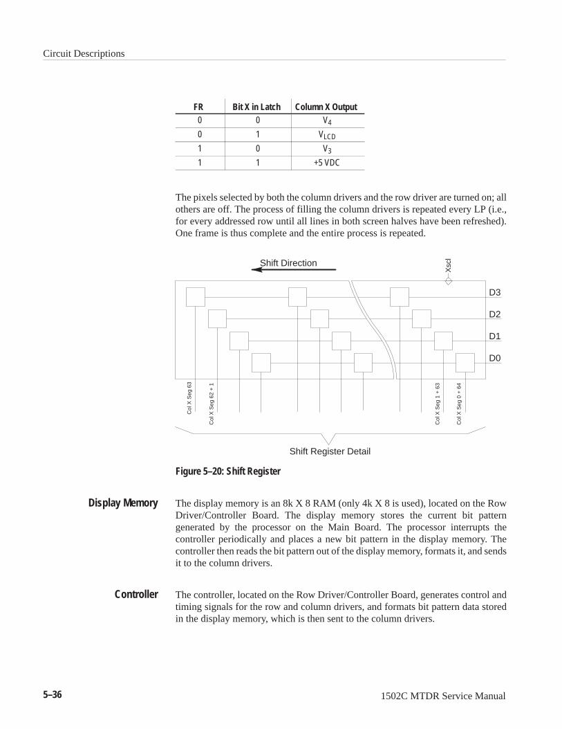
Circuit Descriptions
5–36 1502C MTDR Service Manual
FR Bit X in Latch Column X Output0 0 V4
0 1 VLCD
1 0 V3
1 1 +5 VDC
The pixels selected by both the column drivers and the row driver are turned on; allothers are off. The process of filling the column drivers is repeated every LP (i.e.,for every addressed row until all lines in both screen halves have been refreshed).One frame is thus complete and the entire process is repeated.
Shift Direction
Shift Register Detail
Col
X S
eg 6
3
Col
X S
eg 6
2 +
1
Xsc
l
D3
D2
D1
D0
Col
X S
eg 1
+ 6
3
Col
X S
eg 0
+ 6
4
Figure 5–20: Shift Register
The display memory is an 8k X 8 RAM (only 4k X 8 is used), located on the RowDriver/Controller Board. The display memory stores the current bit patterngenerated by the processor on the Main Board. The processor interrupts thecontroller periodically and places a new bit pattern in the display memory. Thecontroller then reads the bit pattern out of the display memory, formats it, and sendsit to the column drivers.
The controller, located on the Row Driver/Controller Board, generates control andtiming signals for the row and column drivers, and formats bit pattern data storedin the display memory, which is then sent to the column drivers.
Display Memory
Controller

Circuit Descriptions
1502C MTDR Service Manual 5–37
The function of the controller is to read bit pattern data from the display memoryand format it. This data is then sent (along with control and timing signals) to thecolumn and row drivers, which drive the LCD to provide the pattern on the display.
The row driver requires a start pulse at the beginning of each frame, 64 latch pulsesfollowing that to scan the start pulse down the rows, and a framing signal to generatethe AC select voltage. These signals are generated by the controller as shown in therow driver timing diagram (Figure 5–18).
The controller, running at a clock rate of 0.625 MHz, generates ST, LP, and FR withthe following periods:
ST 8 ms
LP 125 s
FR 16 ms
NOTE. The manufacturer’s nomenclature on the controller differs somewhat: ST = FRP, LP = LIP, and FR = FRMB.
Thee column drivers require more control and timing signals than the row driver.These include: EIN, ECLK, XSCL, D3 – D0, LP, and FR.
EIN is required at the start of every line to enable the first (leftmost, as seen from thefront of the display) column driver pair.
ECLK is required once to latch in EIN and three times after that to enable thesuccessive column driver pairs. Each successive ECLK must occur every 16 XSCLpulses (i.e., after each column driver pair is full of 64 bits (4 X 16 bits)).
XSCL is required 16 times per column driver pair per line to shift in the bit patterndata. Therefore, a total of 64 XSCL are required per line for the four column driverpairs.
XSCL is generated by U3030, a counter clocked by CLP or LP from the controller.It must be generated as such because the controller was designed to use with80-channel column drivers instead of 64-channel column drivers. The controllerversion of ECLK, CE0, is generated every 20 XSCL pulses rather than every 16XSCL pulses as required by the 64-channel column drivers. The counter is used totranslate XSCL into ECLK.
As a consequence of generating ECLK as above, EIN must also be generated. Thisis done with the U3065 flip-flop pair. The flip-flop pair is set when LP and LE0 areasserted and hold set until XSCL (CLP) shifts in a logic 0 after the pulse. EIN is heldhigh for a duration long enough to enable the first column driver pair.
Row Driver Interface
Column Driver Interface

Circuit Descriptions
5–38 1502C MTDR Service Manual
There are two data buses and two address buses on the controller. The first data bus,DB7 – DB0, is used to access registers internal to the controller. These internalregisters are used to initialize the controller.
The second data bus, RD7 – RD0, is used to read bit pattern data from the displaymemory. The data bus from the display memory is tied directly to the RD7 – RD0data bus, and indirectly through a bidirectional bus transceiver, U1050, to the DB7– DB0 data bus. The DB7 – DB0 data bus is tied directly to the CPU data bus throughthe 40-pin connector.
The first address bus, MA12 – MA0, is tied to the display memory and addressesit. MA12 – MA0 can have one of two sources. The first is an internal address in thecontroller, which is the address of the currently accessed bit pattern data byte. Thesecond is the address resent on the second address bus, A11 – A0.
This second address bus is tied to the CPU address bus through the 40-pin connectorand is used to address the display memory during the time the CPU is updating thedisplay memory.
The control signal DIEN controls the multiplexing of the internal address and A11– A0 to MA12 – MA0. A15 – A12 are tied low.
There are several other relevant control signals to the controller: CS <chip select>,WR <write>, and RD <read>.
CS and WR are used in conjunction with A0 to write to the internal registers. CSand RD in conjunction with A0 to read them.
XT is the system clock, from which all timing in the controller is derived. It issupplied via the 40-pin connector at 0.625 MHz.
DRAM <display memory select> is used with WR by the CPU to select and writeto the display memory. DRAM and RD are used to read.
The combinational logic associated with the selection of the display memory is suchthat the memory is set to the selected read mode at all times except when the CPUaccesses it. In that case, it could be either selected read or selected write at thediscretion of the CPU. This combinational logic also controls the flow of datathrough the transceiver.
CPU and Display MemoryInterface

Circuit Descriptions
1502C MTDR Service Manual 5–39
CS
PRAM
RD
WR
WR
0E
RD
WR
on RAM
on RAM
D7-D0
Read Data from
Internal Register
Write Data to
Internal Register
Read and Write for Internal Register Timing
Read Data fromDisplay Memory
to CPU
Read Data fromDisplay Memory
to Controller
Write Data toDisplay Memory
from CPU
Figure 5–21: CPU and Display Memory Interface
Circuit Descriptions
5–40 1502C MTDR Service Manual
In operation, the controller is usually accessing the display memory and refreshingthe screen with the bit pattern data. At the rate of about 10 Hz, the CPU intervenesin the refresh operation to update the bit pattern display memory. This operationoccurs as a block transfer of 4k X 8 from the CPU memory to the display memory.This block transfer takes place in about 17 ms. During thew block transfer, thecontroller cannot access display memory and, therefore, sends null data to thescreen.
Because the LCD display is non-emitting, a light source is needed for low lightapplications. This source is provided by an electroluminescent (EL) backlightbehind the transflector. The EL backlight is a long-life device, requiring a 130 VAC,400 Hz supply. This supply is routed from the Front Panel Board through the 40-pinconnector to pads on the Row Driver/Controller Board. The leads on the backlightare then attached to these pads.
CAUTION. The pads for the EL backlight are exposed when the display module isremoved from the front panel. They operate from a high voltage source. Do not turnon the backlight when the pads are exposed.
Because the LCD display response time slows down rapidly at temperatures below+10° C, a heater is required to maintain the temperature of the LCD cell at +10° Cwhen the ambient temperature falls below +10° C.
The heating element is a resistive plating of indium tin oxide (ITO) on the back sideof the row pane. This plating has a resistance of about 64 . The power for the heateris supplied through the 40-pin connector to pads on the Row Driver/ControllerBoard, similar to those for the EL backlight.
A thermistor, RT1030, is attached to the lip of the row pane opposite the cable. Thisthermistor is used to track the temperature of the LCD cell and turn on the heaterpower (+16 VDC) when the temperature falls below +5° C. With a supply voltageof +16 VDC, the heater dissipates about 4W. The circuitry to control the temperatureis located on the Front Panel Board. The thermistor leads are attached to pads on theRow Driver/Controller Board, similar to the heater, and routed through the 40-pinconnector.
ElectroluminescentBacklight
Indium Tin Oxide Heater

1502C MTDR Service Manual 6–1
Calibration
IntroductionThis chapter is divided into the Calibration Performance Check and the AdjustmentProcedure.
The Calibration Performance Check is a series of checks to compare the instrumentparameters to the published specifications. This procedure is similar to the OperatorPerformance Check (Chapter 2), but additionally lists actions to take if theCalibration Performance Check is not met.
The Adjustment Procedure is a series of steps designed to bring the instrument upto standards after repair or performance check.
Calibration Performance Check
The purpose of this procedure is to assure that the instrument is in good workingcondition and should be performed on an instrument that has been serviced orrepaired, as well as at regular intervals.
This procedure is not intended to familiarize you with the instrument. If you are notexperienced with this instrument, you should read the Operation chapter of thismanual before going on with these checks.
If the instrument fails any of these tests, it should be calibrated or otherwiseserviced. Many failure modes affect only some functions of the instrument.
Equipment Tek Part Number50 precision terminator 011–0123–00
3-ft precision coaxial cable 012–1350–00
Disconnect any cables from the front panel CABLE connector. Connect theinstrument to a suitable power source (a fully charged optional battery or AC linesource). If you are using AC power, make sure the fuse and power selector switchon the rear panel are correct for the voltage you are using (115 VAC requires adifferent fuse than 230 VAC).
Option 05 (metric) instruments default to m/div instead of ft/div. You can changethis in the Setup menu, or you may use the metric numbers provided. To change thereadings to ft/div, press the MENU button. Scroll down to Distance/Div is: m/div
Equipment Required
Getting Ready
Metric Instruments
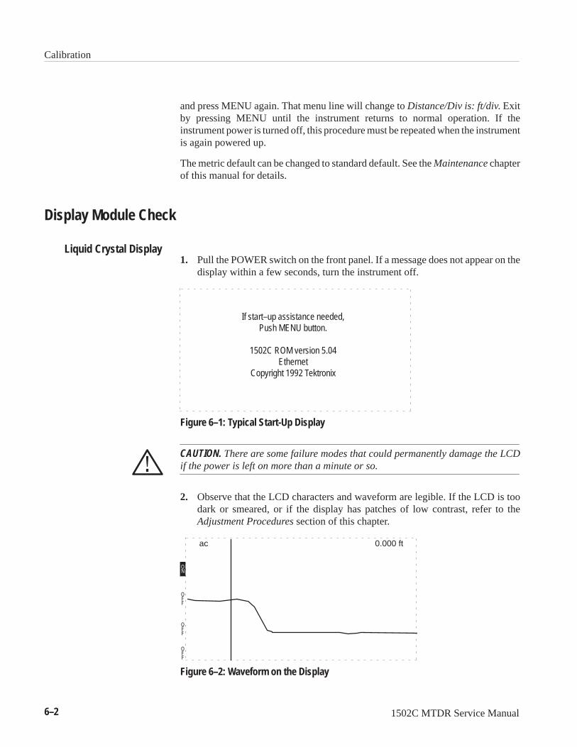
Calibration
6–2 1502C MTDR Service Manual
and press MENU again. That menu line will change to Distance/Div is: ft/div. Exitby pressing MENU until the instrument returns to normal operation. If theinstrument power is turned off, this procedure must be repeated when the instrumentis again powered up.
The metric default can be changed to standard default. See the Maintenance chapterof this manual for details.
Display Module Check
1. Pull the POWER switch on the front panel. If a message does not appear on thedisplay within a few seconds, turn the instrument off.
If start–up assistance needed,Push MENU button.
1502C ROM version 5.04Ethernet
Copyright 1992 Tektronix
Figure 6–1: Typical Start-Up Display
CAUTION. There are some failure modes that could permanently damage the LCDif the power is left on more than a minute or so.
2. Observe that the LCD characters and waveform are legible. If the LCD is toodark or smeared, or if the display has patches of low contrast, refer to theAdjustment Procedures section of this chapter.
OFF
OFF
OFF
ON
ac 0.000 ft
Figure 6–2: Waveform on the Display
Liquid Crystal Display

Calibration
1502C MTDR Service Manual 6–3
NOTE. If the LCD does not appear to be working properly, refer to theTroubleshooting section in the Maintenance chapter as well as the CircuitDescription chapter of this manual.
The EL backlight should come on with power up. The LCD will have a light-greenglow.
1. Press MENU.
2. Use the
POSITION control to scroll to Setup Menu.
3. Press MENU again.
4. Use the
POSITION control to scroll to Light is: ON.
Exit Setup MenuAcquisition Control MenuVertical Scale is: DecibelsDistance/Div is: ft/divLight is: ON
Move Position to select, then push MENU button
Figure 6–3: Setup Menu
5. Press MENU. The EL backlight should go off and the menu line will change toLight is: OFF.
6. Scroll to Light is: OFF and press MENU to turn the light back on.
7. Press MENU again to exit the Setup Menu.
8. Press MENU again to exit the Main Menu.
You should be able to read the LCD in all conditions of illumination, from fullsunlight to a darkened room. The EL backlight might very gradually begin todecrease in brightness after approximately 3,000 hours of use.
NOTE. If the EL Backlight is dim or does not work properly, refer to theTroubleshooting section or the EL Backlight Replacement section in theMaintenance chapter of this manual.
EL Backlight

Calibration
6–4 1502C MTDR Service Manual
Front Panel CheckIf the instrument fails any of these checks, measurements corresponding to the failedcontrol might be inaccurate or unobtainable.
1. Set the front-panel controls:
CABLE No connectionNOISE FILTER Full CWVERT SCALE Default (see note below)DIST/DIV Full CWVP .30POWER Off
NOTE. A default setting is where the instrument will be set when power is switchedon. For example, VERT SCALE will always be 0.00 dB when the instrument ispowered on.
2. Turn POWER on. Wait for initialization and normal operation display.
3. Press MENU.
4. Use the
POSITION control to scroll to Diagnostics Menu.
Return to Normal OperationHelp with Instrument ControlsCable Information MenuSetup MenuDiagnostics MenuView Stored Waveform SettingsOption Port Menu
Move Position to select, then push MENU button
Figure 6–4: Main Menu
5. Press MENU. This will display the Diagnostics Menu.
Presets and Menu Access

Calibration
1502C MTDR Service Manual 6–5
Exit Diagnostics MenuService Diagnostic MenuFront Panel DiagnosticLCD Diagnostics MenuChart Diagnostics Menu
Move Position to select, then push MENU button
Figure 6–5: Diagnostics Menu
6. Use the
POSITION control to scroll to Front Panel Diagnostic.
7. Press MENU. This will display the Front Panel Diagnostics.
1. Press VIEW INPUT. The LCD switch reading should change to 1 (see Figure6–6, third line of text).
Front Panel Diagnostic, test all switches.Hold down MENU button to Exit.Switch: 1 temp: 85Vp: 0.30
Control
Control
Vertical Scale
76
97
230
253
255
61
Switch Reading
Figure 6–6: Front Panel Diagnostic Display
2. Press VIEW STORE. The LCD switch reading should change to 2.
3. Press VIEW DIFF. The LCD switch reading should change to 3.
4. Press STORE. The LCD switch reading should change to 4.
5. Rotate NOISE FILTER counterclockwise to VERT SET REF. The switchreading on the display should be 5.
6. Slowly rotate this control clockwise to its far stop. Each position shouldincrease the switch reading one count, starting at 5 and ending with 14.
Pushbutton Switches
Rotating Controls

Calibration
6–6 1502C MTDR Service Manual
7. Rotate DIST/DIV counterclockwise to its far stop. The switch reading on thedisplay should be 15.
8. Slowly rotate this control clockwise to its far stop. Each position shouldincrease the switch reading one count, starting at 15 and ending with 25.
9. The display should currently show a VP of 0.30. Slowly rotate the left VP controlto full clockwise. Each click should correspond to the front-panel controlsetting.
10. Rotate the right VP control to full clockwise. Again, the LCD reading shouldmatch the front-panel control setting. The final reading with both controls fullyclockwise should be 0.99.
Front Panel Diagnostic, test all switches.Hold down MENU button to Exit.Switch: 1 temp: 84Vp: 0.30
Control
Control
Vertical Scale
142
11
190
0
181
24
Vp Reading
Figure 6–7: Front Panel Diagnostic Display
11. Rotate the
POSITION control, slowly in either direction. The bar graphshown on the display represents the two elements of each control. The readingsto the right of the bar graph represent numbers used by the instrument tocalculate the position of the knob. As the control is rotated, these values and thebar graph will change. The lower value in each column should be between 0 and10 while the higher number is between 245 and 255.
Front Panel Diagnostic, test all switches.Hold down MENU button to Exit.Switch: 35 temp: 82Vp: 0.99
Control
Control
Vertical Scale
0
12
172
142
181
8
Bar Graph
CorrespondingNumbers
Figure 6–8: Front Panel Diagnostic Display

Calibration
1502C MTDR Service Manual 6–7
12. Rotate the
POSITION control slowly in either direction. The lower value ineach column should be between 0 and 10 while the higher number is between245 and 255.
13. Rotate the VERT SCALE control slowly in either direction. The lower valuein each column should be between 0 and 10 while the higher number is between245 and 255.
There is a numerical reading from the thermistor located on the LCD. If it is notoperating properly, the LCD heater might not come on in cold environments. Thiscould result in slow or unreadable displays.
1. The displayed temperature reading should be between 50 and 90, depending onthe ambient temperature. If the thermistor is defective, the reading will be near0 or 255.
Front Panel Diagnostic, test all switches.Hold down MENU button to Exit.Switch: 1 temp: 78Vp: 0.30
Control
Control
Vertical Scale
142
11
190
0
181
24
TemperatureReading
Figure 6–9: Front Panel Diagnostic Display
2. Press MENU repeatedly until the instrument returns to normal operation.
If any of the controls or functions are defective or indicate erratic response, thefunction affected by that control could be in error. The defective control should bereplaced. See the Maintenance chapter of this manual.
Horizontal Scale (Timebase) CheckIf the instrument fails this check, it must be repaired before any distancemeasurements are made with it.
1. Set the front-panel controls:
CABLE No connection (see text)NOISE FILTER 1 avgVERT SCALE 500 m
DIST/DIV .1 ft/divVP .66
Thermistor
Conclusion

Calibration
6–8 1502C MTDR Service Manual
2. Turn on the instrument. The display should look very similar to Figure 6–10.
OFF
OFF
OFF
ON
ac 0.000 ft
Figure 6–10: Waveform on the Display with No Cable Attached
3. Press STORE.
4. Connect the 3-ft precision test cable to the front-panel CABLE connector.
5. Press VIEW DIFF.
6. Rotate NOISE FILTER to HORZ SET REF. The display should look like Figure6–11.
OFF
ON
ac 0.000 ft
ON
ON
move cursor to reference and Press STORE
Figure 6–11: Display with 3-ft Cable and Stored Waveform
7. Using the
POSITION control, set the cursor on the rising edge of thewaveform at the first graticule up from the centerline.
8. Press STORE.

Calibration
1502C MTDR Service Manual 6–9
OFF
ON
ac 0.108 ft
ON
ON
move cursor to reference and Press STORE
Figure 6–12: Cursor on Rising Edge of Pulse
9. Rotate NOISE FILTER back to 1 avg.
10. Press STORE. The front panel reference has now been set.
OFF
ON
ac 0.000 ft
OFF
OFF
Figure 6–13: Cursor at 0.000 ft
11. Rotate the
POSITION control to the rising edge of the waveform, onegraticule above the centerline. This measures the distance from the set point tothe end of the 3-ft cable. The measured distance should be between 2.87 and3.13 feet.
OFF
ON
ac
OFF
OFF
2.988 ft
Figure 6–14: Cursor on Rising Edge of Pulse
12. Remove the 3–ft cable and connect the 50 terminator.

Calibration
6–10 1502C MTDR Service Manual
13. Set the DIST/DIV control to 200 ft/div.
14. Rotate the
POSITION control clockwise until the display distance windowshows a distance greater than 2,000.000 ft. The waveform should remain flatfrom zero to this distance.
OFF
OFF
OFF
ON
ac 2043.000 ft
Figure 6–15: Flatline Display to >2,000 ft
NOTE. If the Timebase does not appear to be working properly, refer to the CircuitDescriptions chapter and the Troubleshooting section of the Maintenance chapterof this manual.
Zero Offset CheckIf the instrument fails this check, you might still make some tests, but the offsetmight change when cable conditions change.
1. Set the front-panel controls:
CABLE (see * below)NOISE FILTER 1 avgVERT SCALE 500 m
DIST/DIV .2 ft/divVP .99POWER ON
* Nothing should be connected to the front panel CABLE connector.
2. Adjust the
POSITION control so the distance window reads –2.000 ft.
3. Use the
POSITION control to center the baseline before the incident pulse.
4. Increase VERT SCALE to 10 m using the
POSITION control to keep thebaseline centered on the display.

Calibration
1502C MTDR Service Manual 6–11
OFF
OFF
OFF
ON
ac –2.000 ft
Figure 6–16: Incident Pulse at –2.000 ft
5. The front panel CABLE connector has a shorting bar that shorts the input whena cable is removed. Attach the 3-ft precision cable to the CABLE connector todefeat this shorting bar.
6. Notice any minor changes in the waveform. The waveform prior to the leadingedge might change shape slightly, but should not shift more than one division.
OFF
OFF
OFF
ON
ac –2.000 ft
Figure 6–17: Incident Pulse at –2.000 ft with 3-ft Cable Connected
Max Hold can be used to easily monitor any changes, as shown below.
OFF
OFF
OFF
ON
ac –2.000 ft
Figure 6–18: Incident Pulse at –2.000 ft with Max Hold
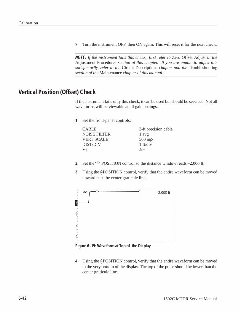
Calibration
6–12 1502C MTDR Service Manual
7. Turn the instrument OFF, then ON again. This will reset it for the next check.
NOTE. If the instrument fails this check,, first refer to Zero Offset Adjust in theAdjustment Procedures section of this chapter. If you are unable to adjust thissatisfactorily, refer to the Circuit Descriptions chapter and the Troubleshootingsection of the Maintenance chapter of this manual.
Vertical Position (Offset) CheckIf the instrument fails only this check, it can be used but should be serviced. Not allwaveforms will be viewable at all gain settings.
1. Set the front-panel controls:
CABLE 3-ft precision cableNOISE FILTER 1 avgVERT SCALE 500 m
DIST/DIV 1 ft/divVP .99
2. Set the
POSITION control so the distance window reads –2.000 ft.
3. Using the
POSITION control, verify that the entire waveform can be movedupward past the center graticule line.
OFF
OFF
OFF
ON
ac –2.000 ft
Figure 6–19: Waveform at Top of the Display
4. Using the
POSITION control, verify that the entire waveform can be movedto the very bottom of the display. The top of the pulse should be lower than thecenter graticule line.

Calibration
1502C MTDR Service Manual 6–13
OFF
OFF
OFF
ON
ac –2.000 ft
Figure 6–20: Waveform at Bottom of the Display
5. Remove the 3-ft precision cable.
6. Connect the 50 terminator to the CABLE connector.
7. Center the pulse in the display. The pulse should be two divisions high.
OFF
OFF
OFF
ON
ac –2.000 ft
Figure 6–21: Waveform at Centered
NOTE. If the instrument fails this check, refer to the Troubleshooting section of theMaintenance chapter of this manual.
Noise CheckIf the instrument fails this check, it might still be usable for measurements of largefaults that do not require a lot of gain. A great deal of noise reduction is availablewith the NOISE FILTER control.
1. Set the front-panel controls:
CABLE 50 terminatorNOISE FILTER 1 avgVERT SCALE 500 m
DIST/DIV 10 ft/divVP .99
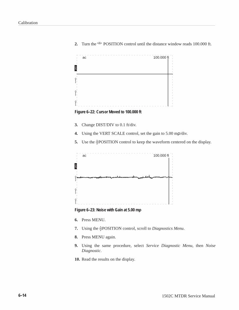
Calibration
6–14 1502C MTDR Service Manual
2. Turn the
POSITION control until the distance window reads 100.000 ft.
ON
ac 100.000 ft
OFF
OFF
OFF
Figure 6–22: Cursor Moved to 100.000 ft
3. Change DIST/DIV to 0.1 ft/div.
4. Using the VERT SCALE control, set the gain to 5.00 m/div.
5. Use the
POSITION control to keep the waveform centered on the display.
ON
ac 100.000 ft
OFF
OFF
OFF
Figure 6–23: Noise with Gain at 5.00 m
6. Press MENU.
7. Using the
POSITION control, scroll to Diagnostics Menu.
8. Press MENU again.
9. Using the same procedure, select Service Diagnostic Menu, then NoiseDiagnostic.
10. Read the results on the display.

Calibration
1502C MTDR Service Manual 6–15
Noise DiagnosticContinuous Result Update
Acceptable Range Result0 – 11 Pixels 4
vertical scale at 5.00 m
and cursor at location to sample.– Push MENU button to Exit –
Figure 6–24: Noise Diagnostic Display
NOTE. If the instrument does not meet this specification, refer to the CircuitDescriptions chapter and the Troubleshooting section of the Maintenance chapterof this manual.
11. Press MENU once to return to the Service Diagnostic Menu. Do not exit fromthe Service Diagnostic Menu because you will use it in the next check.
Sampling Efficiency CheckIf the instrument fails this check, the waveforms might not look normal. If theefficiency is more than 100%, the waveforms will appear noisy. If the efficiency isbelow the lower limit, the waveform will take longer (more pixels) to move fromthe bottom to the top of the reflected pulse. This smoothing effect might completelyhide some events that would normally only be one or two pixels wide on the display.
1. While in the Service Diagnostic Menu, select the Sampling EfficiencyDiagnostic and follow the directions shown on the display.
Exit Service Diagnostic MenuSampling Efficiency DiagnosticNoise DiagnosticImpedance DiagnosticOffset/Gain DiagnosticRAM/ROM DiagnosticsTimebase is: Normal – Auto Correction
Move Position to select, then push MENU button
Figure 6–25: Service Diagnostic Menu

Calibration
6–16 1502C MTDR Service Manual
Sampling Efficiency DiagnosticContinuous Result Update
Acceptable Range Result 50% – 90% 63%
– Push MENU button to Exit –
Figure 6–26: Sampling Efficiency Diagnostic
NOTE. If the instrument does not pass this check, refer to the Circuit Descriptionschapter and the Troubleshooting section of the Maintenance chapter of this manual.
2. Press MENU once to return to the Service Diagnostic Menu. Do not exit fromthe Service Diagnostic Menu because you will use it in the next check.
Offset/Gain CheckIf the instrument fails this check, it should not be used for loss or impedancemeasurements.
1. While in the Service Diagnostic Menu, select the Offset/Gain Diagnostic andfollow the directions shown on the display.
Exit Service Diagnostic MenuSampling Efficiency DiagnosticNoise DiagnosticImpedance DiagnosticOffset/Gain DiagnosticRAM/ROM DiagnosticsTimebase is: Normal – Auto Correction
Move Position to select, then push MENU button
Figure 6–27: Service Diagnostic Menu
NOTE. The 48 dB step might fail intermittently. If a more accurate reading is desired,TP9041 on the Main Board or TP1061 on the Driver/Sampler Board must begrounded during the check. See the Maintenance chapter for the case and EMIshield removal instructions.
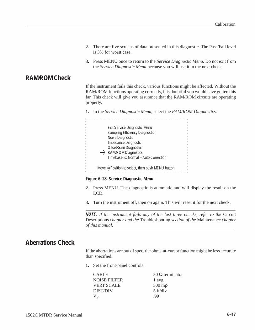
Calibration
1502C MTDR Service Manual 6–17
2. There are five screens of data presented in this diagnostic. The Pass/Fail levelis 3% for worst case.
3. Press MENU once to return to the Service Diagnostic Menu. Do not exit fromthe Service Diagnostic Menu because you will use it in the next check.
RAM/ROM CheckIf the instrument fails this check, various functions might be affected. Without theRAM/ROM functions operating correctly, it is doubtful you would have gotten thisfar. This check will give you assurance that the RAM/ROM circuits are operatingproperly.
1. In the Service Diagnostic Menu, select the RAM/ROM Diagnostics.
Exit Service Diagnostic MenuSampling Efficiency DiagnosticNoise DiagnosticImpedance DiagnosticOffset/Gain DiagnosticRAM/ROM DiagnosticsTimebase is: Normal – Auto Correction
Move Position to select, then push MENU button
Figure 6–28: Service Diagnostic Menu
2. Press MENU. The diagnostic is automatic and will display the result on theLCD.
3. Turn the instrument off, then on again. This will reset it for the next check.
NOTE. If the instrument fails any of the last three checks, refer to the CircuitDescriptions chapter and the Troubleshooting section of the Maintenance chapterof this manual.
Aberrations CheckIf the aberrations are out of spec, the ohms-at-cursor function might be less accuratethan specified.
1. Set the front-panel controls:
CABLE 50 terminatorNOISE FILTER 1 avgVERT SCALE 500 m
DIST/DIV 5 ft/divVP .99

Calibration
6–18 1502C MTDR Service Manual
2. Using the
POSITION control, adjust the distance window to read –2.000 ft.
ON
ac –2.000 ft
OFF
OFF
OFF
Figure 6–29: Waveform with Cursor at –2.000 ft
3. Increase DIST/DIV to 50 m/div.
4. Center the pulse on the display, keeping the trailing baseline on the centergraticule
ON
ac 1.160 ft
OFF
OFF
OFF
Figure 6–30: Waveform at 50 m/div
5. Set the DIST/DIV control to 0.2 ft/div.
6. Adjust the
POSITION control until the rising edge of the pulse is in theleft-most major division on the display.
7. Move the cursor to 0.000 ft with the
POSITION control. All the aberrationexcept the one under the cursor should be within one division of the centergraticule line (see Figure 6–31).

Calibration
1502C MTDR Service Manual 6–19
ON
ac 0.000 ft
OFF
OFF
OFF
Figure 6–31: Waveform at 5 m/div
8. Increase the DIST/DIV to 200 ft/div.
9. Increase the VERT SCALE to 5.00 m.
10. Verify the the waveform is flat one minor division after the incident step.
NOTE. If the instrument fails this check, refer to Driver/Sampler in the CircuitDescriptions chapter and the Troubleshooting section of the Maintenance chapter.
Risetime CheckIf the risetime is out of specification, it might be difficult to make accurateshort-distance measurements near the front panel and might affect the resolution ofthe instrument.
1. Set the front-panel controls:
CABLE 50 terminatorNOISE FILTER 1 avgVERT SCALE 500 m
DIST/DIV 0.1 ft/divVP .99
OFF
ON
ac
OFF
OFF
–0.316 ft
Figure 6–32: Incident Pulse at Center of Display
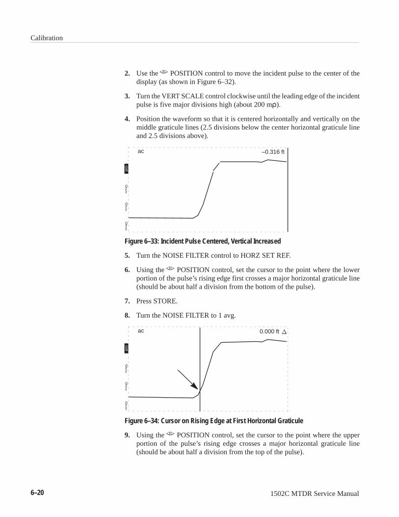
Calibration
6–20 1502C MTDR Service Manual
2. Use the
POSITION control to move the incident pulse to the center of thedisplay (as shown in Figure 6–32).
3. Turn the VERT SCALE control clockwise until the leading edge of the incidentpulse is five major divisions high (about 200 m).
4. Position the waveform so that it is centered horizontally and vertically on themiddle graticule lines (2.5 divisions below the center horizontal graticule lineand 2.5 divisions above).
OFF
ON
ac
OFF
OFF
–0.316 ft
Figure 6–33: Incident Pulse Centered, Vertical Increased
5. Turn the NOISE FILTER control to HORZ SET REF.
6. Using the
POSITION control, set the cursor to the point where the lowerportion of the pulse’s rising edge first crosses a major horizontal graticule line(should be about half a division from the bottom of the pulse).
7. Press STORE.
8. Turn the NOISE FILTER to 1 avg.
OFF
ON
ac
OFF
OFF
0.000 ft
Figure 6–34: Cursor on Rising Edge at First Horizontal Graticule
9. Using the
POSITION control, set the cursor to the point where the upperportion of the pulse’s rising edge crosses a major horizontal graticule line(should be about half a division from the top of the pulse).

Calibration
1502C MTDR Service Manual 6–21
10. Verify that the distance is less than or equal to 0.096 ft .
OFF
ON
ac
OFF
OFF
0.076 ft
Figure 6–35: Cursor on Rising Edge at Last Horizontal Graticule
NOTE. If the instrument fails this check, refer to Troubleshooting in the Maintenancechapter and Driver/Sampler in the Circuit Descriptions chapter of this manual.
Jitter Check
NOTE. If you have just completed the previous check, the instrument might still bein HORZ SET REF mode. This will not have any effect on the Jitter Check. If youwish to exit HORZ SET REF, either turn the power off and on, re-initializing theinstrument, or follow the directions for HORZ SET REF in the Operator chapter.
1. Set the front-panel controls:
CABLE 50 terminatorNOISE FILTER 1 avgVERT SCALE 500 m
DIST/DIV .1 ft/divVP .99
2. Using the
POSITION and the
POSITION controls, center the rising edgeof the pulse on the center horizontal graticule line.
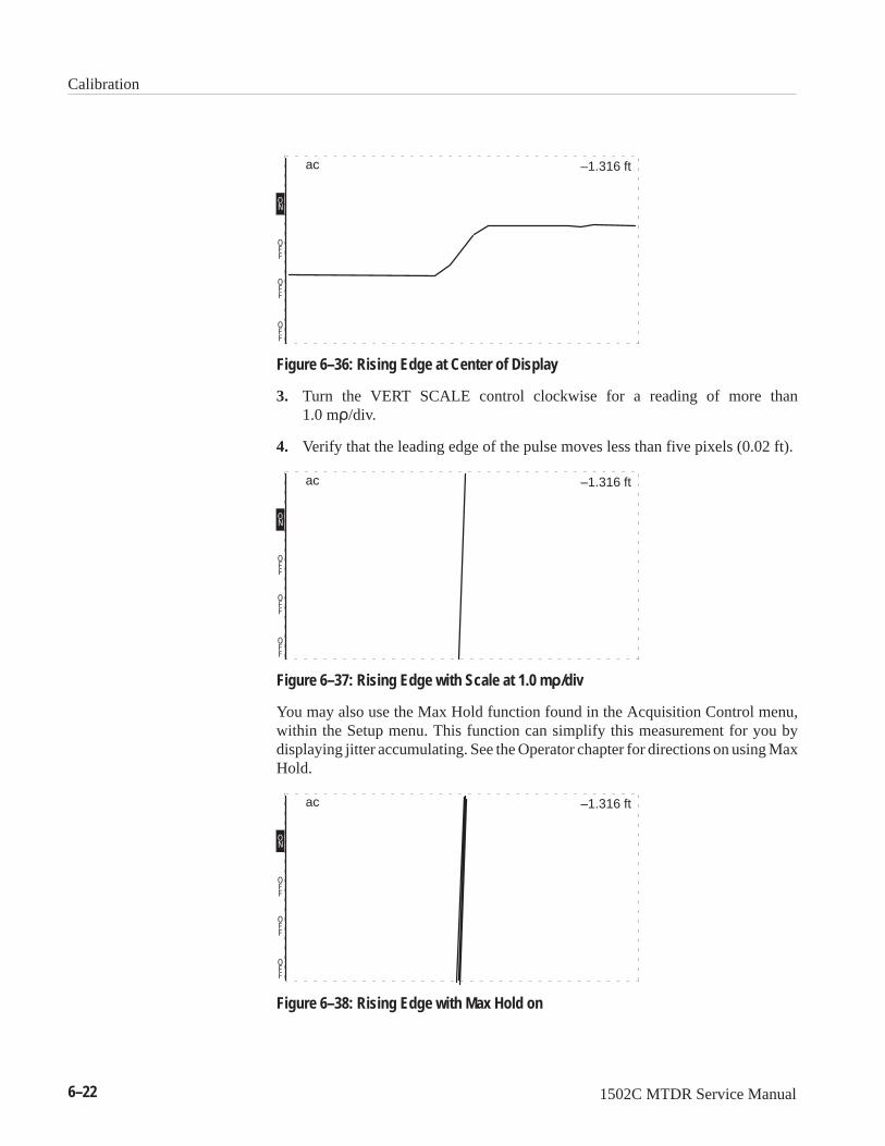
Calibration
6–22 1502C MTDR Service Manual
OFF
ON
ac
OFF
OFF
–1.316 ft
Figure 6–36: Rising Edge at Center of Display
3. Turn the VERT SCALE control clockwise for a reading of more than1.0 m/div.
4. Verify that the leading edge of the pulse moves less than five pixels (0.02 ft).
OFF
ON
ac
OFF
OFF
–1.316 ft
Figure 6–37: Rising Edge with Scale at 1.0 m/div
You may also use the Max Hold function found in the Acquisition Control menu,within the Setup menu. This function can simplify this measurement for you bydisplaying jitter accumulating. See the Operator chapter for directions on using MaxHold.
OFF
ON
ac
OFF
OFF
–1.316 ft
Figure 6–38: Rising Edge with Max Hold on

Calibration
1502C MTDR Service Manual 6–23
Option 04/07: YT-1/YT-1S Chart Recorder CheckIf the instrument does not pass this check, chart recordings might not be possible.
1. Access the Chart Diagnostics Menu found under the Diagnostics Menu.
2. Scroll to Head Alignment Chart and follow the directions.
3. Press MENU to exit this diagnostic.
Figure 6–39: Head Alignment Chart Print
4. There should be approximately six inches of narrow-spaced lines and six inchesof wide-spaced lines. The total length of both should be between 10.87 and12.76 inches. Fold the paper at the last narrow-spaced line and the two endsshould be of equal length (half narrow, half wide).
NOTE. If the chart recorder does not pass this check, refer to the YT-1/YT-1S ChartRecorder Instruction Manual (070–6270–xx) for service information.
Option 05: Metric Default CheckOption 05 requires no check other than to turn on the instrument and see if it displaysin meters. Instructions for changing the default can be found in the Maintenancechapter of this manual.

Calibration
6–24 1502C MTDR Service Manual
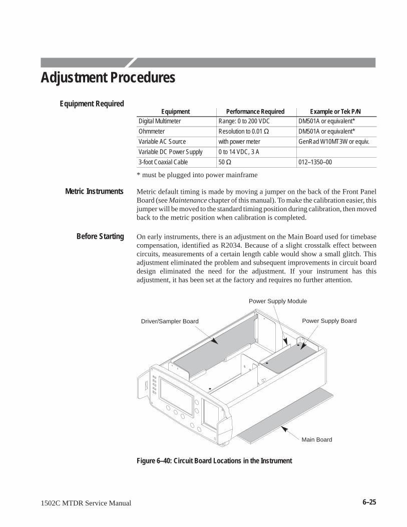
1502C MTDR Service Manual 6–25
Adjustment Procedures
Equipment Performance Required Example or Tek P/NDigital Multimeter Range: 0 to 200 VDC DM501A or equivalent*
Ohmmeter Resolution to 0.01 DM501A or equivalent*
Variable AC Source with power meter GenRad W10MT3W or equiv.
Variable DC Power Supply 0 to 14 VDC, 3 A
3-foot Coaxial Cable 50 012–1350–00
* must be plugged into power mainframe
Metric default timing is made by moving a jumper on the back of the Front PanelBoard (see Maintenance chapter of this manual). To make the calibration easier, thisjumper will be moved to the standard timing position during calibration, then movedback to the metric position when calibration is completed.
On early instruments, there is an adjustment on the Main Board used for timebasecompensation, identified as R2034. Because of a slight crosstalk effect betweencircuits, measurements of a certain length cable would show a small glitch. Thisadjustment eliminated the problem and subsequent improvements in circuit boarddesign eliminated the need for the adjustment. If your instrument has thisadjustment, it has been set at the factory and requires no further attention.
Driver/Sampler Board
Power Supply Module
Power Supply Board
Main Board
Figure 6–40: Circuit Board Locations in the Instrument
Equipment Required
Metric Instruments
Before Starting

Adjustment Procedures
6–26 1502C MTDR Service Manual
To perform the Adjustment Procedure, the instrument must be removed from thecase and the EMI shields removed. Instructions on both procedures are located inthe Maintenance chapter of this manual.
Visual InspectionIf any repairs are made to the instrument, or if it has been disassembled, werecommend a visual inspection be made.
1. Check all screws for tightness and that the screw heads are not burred orrounded.
2. Set the line voltage switch on the rear panel to 110V and check for the properfuse (0.3 A).
3. Check if the LCD has been cleaned on the outside and the implosion shield ofthe front panel has been cleaned on the inside.
4. Check that the knobs and buttons work properly. The NOISE FILTER,DIST/DIV, and both VP knobs have detents; all others should rotate smoothly.Check that the knobs are tight (no loose set screws). Check that the set screwon the POWER switch shaft is tight.
5. Check the cables for proper connection polarity and tightness. Make sure thecables on the front of the Main Board come down from the plug into theinstrument instead of curving toward the outside. All cables should have theexposed ends away from the metal chassis.
6. If any components were replaced by soldering, check for solder balls, excessflux, and wire clippings. Good soldering practices must be followed whenrepairing this instrument.
Power Supply Checks and Adjustments
1. Set the front-panel controls:
NOISE FILTER 1 avg (3rd stop CW)DIST/DIV 1 ft/div (4th stop CW)VP .99
2. Make sure the POWER switch is in the OFF position.
3. Connect the 115 VAC output of the Variac into the AC socket on the rear ofthe 1502C.
Remove the Case and EMIShields
Power-Up Procedure

Adjustment Procedures
1502C MTDR Service Manual 6–27
1. Pull the POWER switch to the ON position.
2. Observe that the power draw does not exceed 4 Watts on the Variac.
Power Supply Board
Figure 6–41: Power Supply Board
3. Connect the positive (+) voltmeter probe to TP1020 (+16.6 VDC – it might bemarked as 15.8 V on some older power supplies).
4. Connect the negative (–) probe to TP1010 (ground).
+
–
J1010
R1010
CR1010
L1010
R1011
R1012
C1011
R1013
C1012
C1013
Q1010
Q1011
C2010
R1015
U1010
R1014
CR1011
Q1012
U1011
VR1012
R1017
C1014
R1018
C1015
C1016
C2013
R1016
R1020R1021
U1020
R1022
R1023
U1021
TP1020
TP1010
Figure 6–42: Power Supply Test Points TP1020 and TP1010
Voltage Checks

Adjustment Procedures
6–28 1502C MTDR Service Manual
5. Verify that the supply voltage is 16.6 VDC and there is a minimal current drawn(< 2W) from the Variac.
6. Connect the positive (+) voltmeter probe to TP2030. The negative (–) voltmeterprobe should remain connected to ground. The reading should be +16.2 VDC(see following table for tolerances).
R2025
R2026
Q2021
Q2022
R2027
C2024CR2021
C2025TP2030
C2031
U2030T1030
R2031
R2032
Q2030
Q2031
CR2030
CR2031
R2030
C2030
Figure 6–43: Power Supply Test Point TP2030
Supply Range Test Point Location+16.2 VDC +15.9 to +16.4 VDC TP2030 Power Supply Board
+5.0 VDC +4.85 to +5.25 VDC Pin 1, J5040 Main Board
–5.0 VDC –4.85 to –5.25 VDC Pin 3, J5040 Main Board
+15.0 VDC +14.7 to +15.3 VDC Pin 4, J5040 Main Board
–15.0 VDC –14..7 to –15.3 VDC Pin 6, J5040 Main Board
7. Make a mental note of the location where the ribbon cable from the powersupply is plugged into the Main Board, then turn the instrument over.
NOTE. When the instrument is turned over, you will be looking at the top (componentside) of the Main Board.
The J5040 pins go through the circuit board and appear on the top (component side)of the Main Board. J5040/P5040 is the input from the power supply. The other endof the cable is J1030/P1030 on the Power Supply Board. Measure the voltages onthe pins listed in the table and verify the supply voltages.

Adjustment Procedures
1502C MTDR Service Manual 6–29
14 2
113
Connector plug P5040on bottom of Main Board.
Connector pin J5040on top of Main Board.
142
1 13
Figure 6–44: Connector Plug P5040 and Pins J5040 on Bottom of Main Board
Test points in this check are located on the Power Supply Board.
1. Connect the positive (+) probe to the +16.6 VDC supply (TP1020) on the PowerSupply Board.
–
J1010
R1010
CR1010
R1011
R1012
C1011
R1013
C1012
C1013
Q1010
R1015
U1010 U1011
VR1012
R1017
C1014
R1016
R1020
R1021
U1020
R1022
TP1020
Figure 6–45: Power Supply Test Point TP1020
2. Change the AC output voltage on the Variac to 132 VAC.
3. Verify that the +16.6 VDC supply remains regulated (+16.4 to +16.8 VDC).
4. Reduce the Variac output voltage to 90 VAC.
5. Verify that the +16.6 VDC supply is still regulated (+16.4 to +16.8 VDC).
6. Move the positive (+) probe to the +16.2 VDC supply (TP2030)
7. Reduce the Variac output voltage until the +16.2 VDC (and the instrument) shutdown. This voltage must be lower than 90 VAC.
Range Check

Adjustment Procedures
6–30 1502C MTDR Service Manual
Q2022
R2027
C2024
CR2021
C2025TP2030
C2031
R2032
Q2030
Q2031
CR2030
CR2031
R2030
Figure 6–46: Power Supply Test Point TP2030
8. Raise the Variac output voltage to 120 VAC. The instrument should remain shutdown.
9. Turn the 1502C POWER off.
Main Board 12 VDC Check and Adjust
Main Board
Figure 6–47: Location of Main Board in Instrument
Test points in this check are located on the Main Board.
1. Turn the instrument over to access the Main Board.
2. Attach the positive (+) probe from the voltmeter to the + side (facing the edgeof the board) of C9031.
3. Attach the negative (–) probe to the other side of C9035.
4. Turn the instrument POWER on and check that less than 4 Watts is drawn fromthe Variac.
5. Adjust R9032 for +12.0 VDC.
+12 VDC

Adjustment Procedures
1502C MTDR Service Manual 6–31
(+)
GND R8043
R8042
R8041
R8040
R9032
R9031
C9035
C9034
C9033
R9030
C9032
U9030
C9031C
9030
C9025
R9027
Q9021
C9024
R9026
R9025
R9024
C9023
R9023
C8022
C8024
R8028
R8027
R8026
CR
8029R
8025C
7022
R7024
R7025
R7026
R7027 Q7021
R7028
C7023
R7030
R7031
R7032
R7033
C2030 Q7030
R7034
Figure 6–48: Main Board Probe Points
Test points in this check are located on the Main Board.
1. Move the positive (+) probe to the ground side of C9035 (the side away fromthe edge of the board).
2. Verify that the voltage is –11.8 to –12.2 VDC.
3. Verify that the LCD shows the following display:
OFF
OFF
OFF
ON
ac 0.000 ft
Figure 6–49: Waveform on Display
You might have to adjust R1018 (Contrast Adjust) on the Front Panel Board to geta clear display (see LCD Check and Adjustments in this section).
–12 VDC

Adjustment Procedures
6–32 1502C MTDR Service Manual
1. Turn the POWER off.
2. Remove the AC plug from the rear panel of the instrument.
3. If a battery is present, disconnect the wire from the battery to the Power Supplyboard.
4. Connect an external 12 VDC power supply into the battery connector (seeFigure 6–50). Pins 1 and 4 are ground. Pins 2 and 3 are positive (supply)terminals.
5. Adjust the external 12 VDC supply for +11.5 VDC output at the terminals ofthe battery input.
6. Connect a DC ammeter in series with the positive (+) side of the 12 VDC supply.
7. Turn the power on. The current measurement must not exceed 350 mA.
Battery
Red
Orange&
Yellow&
Brown
Fuse
Battery Connector J2010
Wire
Power Supply Board
Figure 6–50: Battery Connections to Power Supply Board
8. Connect the positive (+) probe of the voltmeter to the front side of CR2012 onthe Power Supply Board (this is the large diode next to J2010. The positiveprobe should be on the non-banded end of the diode).
9. Connect the negative probe to ground.
DC Power Check

Adjustment Procedures
1502C MTDR Service Manual 6–33
12
3
U2010
CR2015
CR2011
CR2012
J2010
TP2010
(+) CR2012
Figure 6–51: CR2012 on Power Supply Board
10. Turn the 1502C POWER on. The instrument should initialize and go intonormal operation. The display will be normal except ac in the upper left cornerwill have changed to bat.
OFF
OFF
OFF
ON
bat 0.000 ft
Figure 6–52: Display Showing Power is Battery
11. Reduce the output voltage of the DC power supply until bat/low appears in theupper left corner of the display.
OFF
OFF
OFF
ON
bat/low 0.000 ft
Figure 6–53: Display Showing Battery Voltage is Low
12. Verify that the DC supply voltage is between 10.6 and 11.0 VDC.

Adjustment Procedures
6–34 1502C MTDR Service Manual
13. Remove the voltmeter probes from the 1502C.
14. Remove the external 12 VDC power supply cable from the battery connector.
15. Reconnect the battery wire to the Power Supply board and to the battery.
16. Connect the AC supply cord to the rear panel.
(with optional battery)
1. Turn the POWER off.
2. Connect a voltmeter across the 4 resistor, R2012, located on the PowerSupply Board.
3. Connect the positive (+) probe to the side nearest the front panel and thenegative (–) probe to the other end. The voltage drop across R2012 should bebetween 0.4 and 1.2 VDC.
12
3
U2010
CR2015
CR2011
CR2012
J2010
TP2010
L1010
C2012
C2010
Q1012
R2012
R2011
CR2013
CR2014
S2010
R2012
CR2010
Figure 6–54: R2012 on Power Supply Board
4. Turn the POWER on.
The voltage reading across R2012 should change only slightly (10 mV).
NOTE. The charging current will vary according to the level of charge already onthe battery. With a fully charged battery, the voltage across R2012 should beapproximately 0.4 VDC. With a battery below 11 Volts, R2012 should readapproximately 1.2 VDC.
Charging Current Check

Adjustment Procedures
1502C MTDR Service Manual 6–35
Impedance CheckIf the instrument fails this check, it should not be used for loss or impedancemeasurements.
The following test points are located on the Driver/Sampler Board.
Driver/Sampler Board
Figure 6–55: Driver/Sampler Board Location
1. Turn off the POWER to the instrument.
2. Remove the cover of the Driver/Sampler Board (see Maintenance chapter).
C3010 C3011
C1020
C2020C2021
C2022
C2023
C2024
C2031
C2025
C2026
R3032
R3033
TP1020 TP1030
TP1021
TP3020
T1020
C2010
R10
10C
1010
C10
11C
2012
C20
11
CR
3020
CR
3021
C30
20R
3020
R30
21
R10
20
CR
1030
Q10
30
U1010
Figure 6–56: TP1030 on Driver/Sampler Board

Adjustment Procedures
6–36 1502C MTDR Service Manual
3. Using a precision Ohmmeter, measure the resistance from the 0.6 VDC supply(TP1030) to the center conductor of the front-panel CABLE connector.
4. Subtract the resistance of the Ohmmeter test probes. The result should bebetween 49.5 and 50.5 .
LCD Check and Adjustment1. Turn POWER on.
2. Push MENU.
3. Using the
POSITION control, scroll to Diagnostics Menu.
4. Push MENU.
5. Scroll to LCD Diagnostics Menu.
6. Push MENU.
7. Scroll to LCD Alignment Diagnostic.
8. Push MENU.
R1018
Figure 6–57: R1018 on Front Panel Board
9. Observe the LCD as you adjust R1018 (Contrast Adjust) counterclockwise untilthe entire pattern starts to dim.
ÄÄÄÄÄÄÄÄÄÄÄÄÄÄÄÄÄÄÄÄÄÄÄÄÄÄÄÄÄÄÄÄÄÄÄÄÄÄÄÄÄÄÄÄÄÄÄÄÄÄÄÄÄÄÄÄÄÄÄÄÄÄÄÄÄÄÄÄÄÄÄÄÄÄÄÄÄÄÄÄÄÄÄÄÄÄÄÄÄÄÄÄÄÄÄÄÄÄÄÄÄÄÄÄÄÄÄÄÄÄÄÄÄÄÄÄÄÄÄÄÄÄÄÄÄÄÄÄÄÄÄÄÄÄÄÄÄÄÄÄÄÄÄÄÄÄÄÄÄÄÄÄÄÄÄÄÄÄÄÄÄÄÄÄÄÄÄÄÄÄ
Push MENU 1 sec to alternate, 2 secs to quit
Figure 6–58: LCD Pattern with Contrast Too Light

Adjustment Procedures
1502C MTDR Service Manual 6–37
Push MENU 1 sec to alternate, 2 secs to quit
Figure 6–59: LCD Pattern with Contrast Too Dark
10. Turn R1018 clockwise until the entire pattern is clear and sharp.
Push MENU 1 sec to alternate, 2 secs to quit
Figure 6–60: LCD Pattern Adjusted for Sharpness
11. Press MENU once quickly. The ON pixels will be toggled off and the OFFpixels will be toggled on. Watch to see if all the pixels are being activated.
12. Once contrast has been set using the LCD pattern, verify it with a normalwaveform display.
a. Ensure that the instrument has been at 75° F 5° F (25° C 3° C) for atleast one hour (operating or non-operating).
b. Turn the instrument on and allow it to warm up for at least five minutes. Ifthe instrument was already on (e.g., you are performing this adjustmentimmediately after steps 1 – 11), then cycle the power off, then back on againto return it to default settings.
c. While a waveform is on the display, adjust R1018 on the Front Panel Boardcounterclockwise until most of the display has dimmed.

Adjustment Procedures
6–38 1502C MTDR Service Manual
OFF
OFF
OFF
ON
ac 0.000 ft
Figure 6–61: Waveform with Contrast Too Light
d. Start rotating R1018 slowly clockwise until all of the pixels are just visibleon the display. If you go too far, restart the adjustments at step c.
e. Rotate R1018 one quarter turn clockwise past the point of step d.
NOTE. It is important to always determine the proper contrast setting by comingfrom a faded display. It takes a higher threshold voltage to turn a pixel on than itdoes to turn one off. If it is done from the other direction, the display will be toobright.
f. Inspect the display for any bleeding (areas that are too dark) or any fading(areas that are too light).
g. Turn the instrument off.
h. After waiting a few seconds, turn the instrument back on.
i. Reinspect the display for bleeding or fading.
j. Readjust R1018 if necessary.
OFF
OFF
OFF
ON
ac 0.000 ft
Figure 6–62: Waveform with Contrast Adjusted Correctly

Adjustment Procedures
1502C MTDR Service Manual 6–39
If the Contrast Adjust is set properly, you will be able to see the cursor clearly whenit is moved rapidly across the display. If any residual images are made by the cursormovement, they should fade out quickly.
NOTE. If you are unable to adjust the contrast, or if pixels are not functioning, seethe Troubleshooting section in the Maintenance chapter of this manual.
Zero Offset AdjustThe following adjustment is located on the Driver/Sampler Board.
Driver/Sampler Board
Figure 6–63: Driver/Sampler Board Location
1. Turn off the POWER to the instrument.
2. Remove the EMI shield covering the Driver/Sampler Board (see Maintenancechapter).
3. Turn the POWER on.
4. Adjust the
POSITION control until the distance window reads –2.000 ft.
5. Adjust the
POSITION control to center the baseline on the center horizontalgraticule line (see Figure 6–64, next page).
6. Set the front-panel controls:
CABLE no connectionNOISE FILTER 1 avgVERT SCALE 10 m
DIST/DIV 0.2 ft/divVP .99
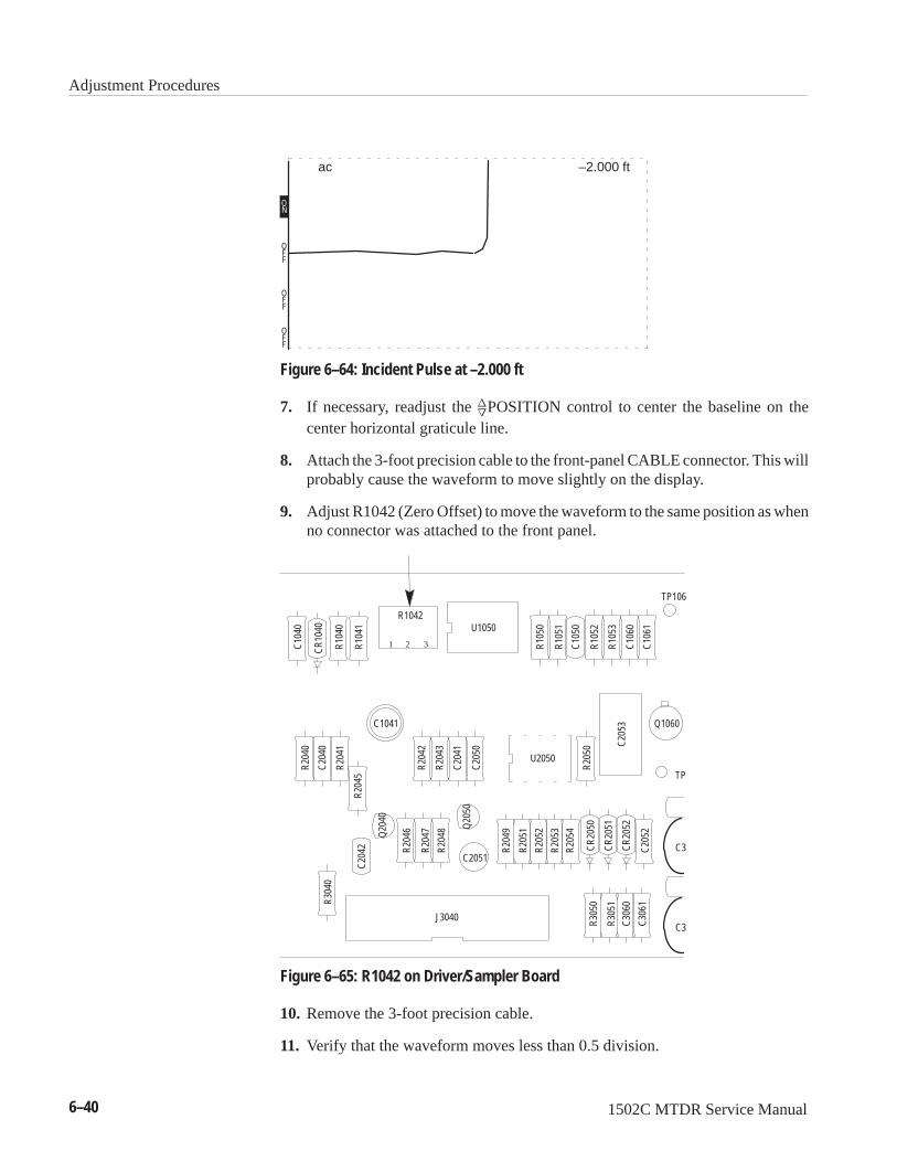
Adjustment Procedures
6–40 1502C MTDR Service Manual
OFF
OFF
OFF
ON
ac –2.000 ft
Figure 6–64: Incident Pulse at –2.000 ft
7. If necessary, readjust the
POSITION control to center the baseline on thecenter horizontal graticule line.
8. Attach the 3-foot precision cable to the front-panel CABLE connector. This willprobably cause the waveform to move slightly on the display.
9. Adjust R1042 (Zero Offset) to move the waveform to the same position as whenno connector was attached to the front panel.
R1042U1050
C1041
U2050
Q1060
TP
C2051
J3040C3
C3
TP106
C10
40
CR
1040
R10
40
R10
41
R10
50
R10
51
C10
50
R10
52
R10
53
C10
60
C10
61
R20
40
C20
40
R20
41
R20
45
R20
42
R20
43
C20
41
C20
50
R20
50
C20
53
R30
40
C20
42
Q20
40
R20
46
R20
47
R20
48
Q20
50
R20
49
R20
51
R20
52
R20
53
R20
54
CR
2050
CR
2051
CR
2052
C20
52
R30
50
R30
51
C30
60
C30
611 2 3
Figure 6–65: R1042 on Driver/Sampler Board
10. Remove the 3-foot precision cable.
11. Verify that the waveform moves less than 0.5 division.

Adjustment Procedures
1502C MTDR Service Manual 6–41
NOTE. Some changes in shape of the baseline before the leading edge is normal. Ifthis measurement is difficult to make, access the Service Diagnostic Menu andchange the timebase mode from Timebase is:Normal – Auto Correction to Timebaseis: Diagnostic – No Correction. This will give more stability to the pulse when thecable is connected.
12. Turn the instrument off.
13. Replace the Driver/Sampler EMI shield. Be sure the ribbon cable is placed inthe center slot of the shield so it won’t be crushed by the shield.
After Adjustments are Completed
1. If the instrument is Option 05 (metric), refer to the Maintenance chapter toreturn the metric default jumper to its proper position.
2. Reinstall the 1502C in its case (refer to the Maintenance chapter of this manual).Care should be taken to follow the directions to maintain watertight integrityof the case.
3. Turn back to the Calibration section of this chapter and perform all thosePerformance Checks that did not require case-off adjustments.

Adjustment Procedures
6–42 1502C MTDR Service Manual

1502C MTDR Service Manual 7–1
Maintenance
IntroductionThis chapter contains information on preventive and corrective maintenance,troubleshooting, panel control assembly procedures, and shipping instructions.Please refer to schematics for physical location of circuits and components.
NOTE. We recommend that service be performed at an authorized Tektronix ServiceCenter or by a technician skilled in sampling and pulse techniques.
This is a list of common tools needed to accomplish all the maintenance proceduresthat follow:
5/16” hex nut driver Phillips-head screwdriver
11/32” hex nut driver Straight-blade screwdriver
1/16” hex wrench Torque driver
5/16” open-end wrench Soldering and desoldering tools
7/16” open-end wrench Cotton swabs, non-woven wipes
1/2” open-end wrench Isopropyl alcohol, LocTite , etc.
Preventive MaintenancePreventive maintenance includes cleaning, visual inspection, and lubrication. Aconvenient time to perform preventive maintenance is during the periodicperformance check/calibration procedure. If the instrument has been subjected toextreme environments or harsh handling, more frequent maintenance might benecessary.
CAUTION. Do not use chemical agents that contain benzene, toluene, xylene,acetone, etc., because of possible damage to plastics in the instrument.
The exterior case and front panel should be washed gently with mild soap and water.
The faceplate in front of the LCD should be cleaned gently with Kendall Webrilnon-woven wipes (Tek P/N 006–0164–00), or equivalent, moistened with isopropylalcohol.
Equipment Required
Cleaning

Maintenance
7–2 1502C MTDR Service Manual
The interior of the 1503C is protected from dirt and dust as long as the option portand case are intact. However, if interior cleaning is necessary, blow off accumulateddust with low-pressure air and remove the remaining dirt with a soft brush, cottonswab, or pipe cleaner moistened with isopropyl alcohol.
All the switches and potentiometers on the 1503C are sealed from externalcontaminants and, therefore, require little maintenance and no lubrication.Occasionally, blowing out accumulated dust is all that is needed.
Obvious defects, such as broken connections, damaged boards, frayed cables,improperly seated components, and heat-damaged components should be correctedfirst before attempting further troubleshooting. Heat damage usually indicates adeeper problem somewhere in the circuitry and should be traced and correctedimmediately.
We do not recommend electrical checks of individual components because defectivecomponents will become evident during instrument operation.
After maintenance has been performed, the instrument should be checked as per theprocedures in the Calibration chapter of this manual.
Part Removal and Replacement
The fuse is accessible through the rear panel of the case.
1. Unscrew the fuse cover and remove.
REMOVE REMOVECAP TO CAP TOSELECT REPLACE
VOLTAGE FUSE
Figure 7–1: Location of Voltage Selector and Fuse Holder on Rear Panel
Lubrication
Visual Inspection
Recalibration
AC Fuse

Maintenance
1502C MTDR Service Manual 7–3
2. Use a straight-blade screwdriver to remove the fuse holder.
3. Check the voltage selector for proper voltage setting. If the instrument voltageselector is set for 115 VAC, replace the fuse with a 0.3 A fuse (Tek P/N159–0029–00). If the voltage selector is set for 230 VAC, replace the fuse witha 0.15 A fuse (Tek P/N 159–0054–00).
4. Replace the fuse holder.
5. Replace the access cover.
1. Remove the instrument front cover.
2. If installed, remove the chart recorder, or other device, from the option port.
3. Loosen the four screws on the back of the case and set the instrument face-upon a flat surface.
4. Swing the handle out of the way of the front panel.
5. Break the chassis seal by pushing downward with both hands on the handlepivots on each side of the case.
6. Grasp the case with one hand and tilt the chassis out with the other. Lift bygrasping the outside perimeter of the front panel.
7. Remove the screw in the middle of the bottom EMI shield. Remove the top andbottom shields from the chassis by carefully running a straight-bladescrewdriver between the shield and the groove in the chassis rail.
CAUTION. Do not lift the instrument by the front-panel controls. The controls willbe damaged if you do so.
1. From the Power Supply Board, remove the 14-conductor ribbon cable. This isa keyed connector, so polarity is guaranteed upon reinstallation (Figure 7–2, 5).
2. Remove the screw and washer located below the power switch on the instrumentside panel (Figure 7–2, 7).
3. Remove the screw and washer holding the power supply module to the bottomchassis (Figure 7–2, 4).
4. Remove two screws holding the power supply module to the rear chassis panel.One is located near the AC power receptacle and the other is directly above thefuse holder (Figure 7–2, 6).
Removal of Case and EMIShields
Removing the PowerSupply Module

Maintenance
7–4 1502C MTDR Service Manual
5. Remove the power supply module from the instrument by moving it toward thefront of the instrument, guiding the power switch away from the mechanicallinkage assembly.
NOTE. The screws identified as 1 hold the circuit board to the module. They shouldnot be removed until you are ready to remove this circuit board from the module (nextprocedure).
1
1
1
1
2 34
6
5
6
7
Top Viewof
Power SupplyModule
End Viewof
Rear Panel
Figure 7–2: Power Supply Module and P/O Rear Panel
1. Remove the power supply module per previous procedure.
2. Remove the two-conductor harmonica connector (Figure 7–2, 3).
3. Remove the four-conductor harmonica connector (Figure 7–2, 2).
Removing the PowerSupply Board

Maintenance
1502C MTDR Service Manual 7–5
4. Remove four screws holding the circuit board to the module (Figure 7–2, 1).
5. Remove the Power Supply Board by carefully lifting up. Be sure the largecapacitor on the bottom of the board clears the two nut blocks on the moduleside panels. If the board or the capacitor binds on either the nut blocks or thechassis side panel screw, remove the nut blocks.
1. Remove the power supply module and circuit board per previous procedures.
2. Remove the three screws holding the side panel on the power supply module.
3. Remove the side panel. This will provide access to the transformer.
4. Unsolder the six wires attached to the power transformer.
5. Unsolder the varistor (R101) from lugs 4 and 5.
6. Remove the two screws and lock-washers holding the power transformer to thechassis.
7. Lift out the transformer.
NOTE. When reassembling, add a small amount of LocTite to the two transformermounting screws in step 6.
1. Remove the power supply module, circuit board, and transformer per previousprocedures.
2. Unsolder the three wires on the filter unit.
3. Remove the two screws and the spacer holding the receptacle.
4. Remove the filter unit from the rear of the module.
1. Remove the power supply module, circuit board, and transformer per previousprocedures.
2. Unsolder all four wires from the voltage selector switch.
3. Unsolder the two wires from the fuse holder.
4. Unscrew the hold-down nuts from both units.
5. Remove both units from the rear of the module.
Removing the PowerTransformer
Removing the Power CordReceptacle
Removing the Fuse Holderand Voltage Selector

Maintenance
7–6 1502C MTDR Service Manual
Conductor Color Alternate ColorUngrounded (line) Brown Black
Grounded (neutral) Blue White
Grounded (earth) Green/Yellow Green
1. Unplug the battery cable at the battery and at the plug on the Power Supplyboard.
2. Remove the two (2) screws securing the battery clamp to the chassis.
3. Remove the battery clamp, making sure not to short the terminals with theclamp.
4. Carefully lift the battery from the chassis.
1. From the top side of the instrument, remove the multi-colored cable (powersupply) from the Main Board.
2. Turn the instrument upside down to expose the top of the Main Board.
3. Remove the three multi-colored cables from the component side of the MainBoard. This can be accomplished by inserting a small straight-bladescrewdriver in the key and gently prying the connector from the board. Take careto guide the connectors straight off to avoid bending the pins.
4. Remove the eight screws and the center spacer post (with washer and locknut)that fasten the Main Board to the chassis.
5. Remove the Main Board, taking care to avoid binding on the power switchmechanical linkage.
NOTE. One of the corner screws (see Figure 7–3) holds a ground strap connector.
Power Cord ConductorColor Code
Removing the Battery
Removing the Main Board

Maintenance
1502C MTDR Service Manual 7–7
Figure 7–3: Main Board
1. Use an IC puller that is designed to extract multi-pin microcircuits to removethe EPROM from its socket.
Front ofInstrument
Figure 7–4: EPROM on Main Board
2. When installing a new EPROM, make sure the notch in the IC is facing towardthe front of the instrument and all pins are inserted correctly in the socket.
EPROM Replacement

Maintenance
7–8 1502C MTDR Service Manual
Typically, the lithium battery for the non-volatile memory will last over seven years.If it requires replacement, use the following procedure.
CAUTION. To avoid personal injury, observe proper procedures for handling anddisposal of lithium batteries. Improper handling might cause fire, explosion, orsevere burns. Do not recharge, crush, disassemble, heat the battery above 212° F(100° C), incinerate, or expose the contents of the battery to water. Dispose of thebattery in accordance with local, state, and federal regulations. Typically, smallquantities (less than 20 batteries) can be safely disposed of with ordinary garbageor in a sanitary landfill, but check local regulations before doing this.
1. Remove the Main Board as described in a previous procedure.
U1011
U1010
Unsolder here
LithiumCell
Unsolder here
Figure 7–5: Lithium Battery on Main Board
2. Unsolder the four leads of the lithium battery, being careful not to overheat thecell.
3. Remove the cell from the Main Board.
4. Install a new battery and solder the leads to the Main Board.
CAUTION. Be sure that the new battery is one that is supplied or authorized byTektronix. An improper replacement cell could cause irreversible damage to theMain Board circuitry.
Lithium BatteryReplacement

Maintenance
1502C MTDR Service Manual 7–9
1. Remove the two screws and washers holding the cover to the chassis.
2. Remove the cover by sliding it toward the center of the instrument. Whenre-assembling, make sure the cable is placed under the slot provided.
3. Disconnect the multi-conductor cable from the circuit board.
4. Remove the coaxial cable from the circuit board.
5. Remove the circuit board from the instrument by sliding it out of the cardguides.
1. Using a hex wrench, disassemble the power switch linkage. This disconnectsthe front-panel switch shaft from the linkage block.
2. Remove the three multi-conductor cables from the Main Board.
3. Remove the Driver/Sampler Board EMI shield.
4. Remove the coaxial cable from the Driver/Sampler Board.
5. Remove the four corner screws on the instrument front panel.
6. Carefully guide the coaxial cable through the Driver/Sampler card cage.
7. Remove the Front Panel Assembly from the instrument chassis.
1. Using the previous procedure, remove the Front Panel Assembly from theinstrument.
2. Remove all knobs.
3. Remove the hex nuts and washers from the front-panel controls.
4. Remove the buttons by pressing gently on the rubber boot behind each button.
CAUTION. Take care not to use a sharp object to remove the buttons because it mightpuncture the rubber boot, thereby subjecting the instrument to moisture/waterintrusion.
Removing theDriver/Sampler Board
Removing the Front PanelAssembly
Removing the DisplayModule/Front Panel Board

Maintenance
7–10 1502C MTDR Service Manual
Figure 7–6: Display Module/Front Panel Board Screw Locations
NOTE. When re-assembling, push the rubber boot down on the switch shaft so thatthe switch button can easily be replaced.
5. Remove the four screws holding the Display Module/Front Panel Board to thefront panel (see Figure 7–6).
6. Carefully lift the Display Module/Front Panel Board from the front panel.
1. Remove the four hex nuts (two are shown in Figure 7–7) that hold the DisplayModule to the Front Panel Board.
2. Disconnect the ribbon cable from the boards.
3. Carefully separate the Display Module from the Front Panel Board.
Figure 7–7: Display Module/Front Panel Board Showing Hex Nuts
Removing the Front PanelBoard from the Display
Module

Maintenance
1502C MTDR Service Manual 7–11
CAUTION. Do not further disassemble the Display Module. Elastomeric splices areused between the circuit boards and they require special alignment fixtures. Partsreplacement requires special surface-mount technology.
The instrument will power up displaying DIST/DIV measurements as meters(m/div) or feet (ft/div). Although either measurement mode may be chosen from theSetup Menu, the default can easily be changed to cause the preferred mode to comeup automatically at power up.
1. Remove the instrument from the case.
2. Remove the bottom EMI shield.
Jumper
Front PanelBoard
Main Board
Ribbon Cable Connectors
Figure 7–8: Location of Default Jumper on Front Panel Board
3. From the bottom side of the instrument, peer into the space between the MainBoard and the Front Panel Board. The default jumper is located behind thescrew that holds the Front Panel Assembly to the front-panel mounting stud.
Standard
Metric
Top of Instrument
Bottom of Instrument
FrontPanelBoard
Jumper
Figure 7–9: Default Jumper Positions
Changing the Default toMetric
Maintenance
7–12 1502C MTDR Service Manual
4. Using a needle-nose plier, slip the jumper off the pins and move it to the desireddefault position (top for meters, bottom for feet).
1. Remove the Power Supply Module as shown in a previous procedure.
2. Remove the Front Panel Assembly as previously described.
3. Remove the ribbon cable on the Main Board that connects the Main Board tothe Option Port Assembly.
4. Remove the screw and washer from the instrument side panel.
5. Remove the nut from the bottom of the instrument.
6. The Option Port Assembly may be disassembled further by removing the fourscrews from the back of the assembly. This will allow easy access forreplacement of the Option Port connector.
Troubleshooting
When encountering difficulties with the instrument, first use the troubleshootingchart in the Operation chapter. This might eliminate any minor problems such asfuse or power problems.
The following troubleshooting flow charts (next three pages) are designed to giveyou an idea where to start. The Circuit Descriptions and Schematics chapters willgive further assistance toward solving the problem.
The Main Board waveforms represented on the flow chart are representative of aninstrument in operation per the setup at the top of the flow chart. Additional MainBoard waveforms are also included in this section.
The following Main Board waveforms are similar to the waveforms found on thetroubleshooting flow chart. In some cases, however, the oscilloscope was set toshow timing rather than the detail of the waveform. For example, TP7010 on theflow chart shows the detail of the pulse, but the same test point in the followingfigures shows the repetition rate.
Set the 1503C front-panel controls:
CABLE Attach 10-ft cableNOISE FILTER 1 avg (3rd position CW)VERT SCALE defaultDIST/DIV 1 ft/div (4th position CW)Vp .84
Removing the Option PortAssembly
Troubleshooting FlowChart
Test Point Waveforms

Maintenance
1502C MTDR Service Manual 7–13
Vertical Position defaultHorizontal Position default
(waveform figures located on page 7–16)

Maintenance
7–14 1502C MTDR Service Manual
Are
wav
efor
m a
nd
STAR
TTr
oubl
esho
otin
gC
hart
- Cas
e O
ff
Che
ck P
ower
Sup
ply
per A
djus
tmen
tPr
oced
ure.
Unp
lug
ribbo
n ca
ble
from
pow
er s
uppl
y.C
ycle
pow
er o
ff/on
.R
eche
ck p
ower
sup
ply
per p
revi
ous
step
.
Che
ck p
ower
sup
ply
mod
ule.
Unp
lug
each
boa
rdto
find
faul
t.
Fix
indi
cate
d bo
ard
or c
ablin
g.
Dis
play
cle
arly
show
s te
xtor
gra
ticul
e?
If di
spla
y bl
ank
or b
lack
,ad
just
con
trast
(R10
14)
per A
djus
tmen
t Pro
cedu
re.
Che
ck d
ispl
aysy
stem
.
No
chan
ge
Inst
rum
ent r
espo
nds
norm
ally
to c
ontro
ls?
Run
fron
t pan
el a
ndR
AM/R
OM
Dia
gnos
is
Che
ck p
roce
ssor
syst
em.
Che
ck fr
ont
pane
l boa
rd.
Che
ck c
hart
reco
rder
or o
ther
ext
rafu
nctio
n m
odul
es.
Run
Cal
ibra
tion
Perfo
rman
ce C
heck
.
Fron
t Pan
eldi
agno
stic
pass
ed.
RAM
/RO
Mdi
agno
stic
won
’t ru
n or
diag
nost
icfa
iled.
Go
toBa
dG
ood
Yes
Yes
No
Goo
d
Bad
No
No
Yes
Set F
ront
Pan
el c
ontro
ls:
CAB
LEN
OIS
E FI
LTER
DIS
T/D
IVVp
Atta
ch 3
-ft c
able
1 av
g (3
rd p
ositi
on C
W)
1 ft/
DIV
(4th
pos
ition
CW
).6
6
2+/
–5V,
+/–
15V,
+16
.2V
mea
sure
men
ts n
orm
al?

Maintenance
1502C MTDR Service Manual 7–15
CONTINUE
Go to
3No
Bad
Good Bad Good
BadGood
Bad
Good
Bad
Good
Good
Bad
Yes
Waveform off top orbottom of display or
wrong height?Waveform flat line?
Check video TP9041on main board
with scope.
Check signal onCABLE with scopeat all pulse widths.
Check pulse strobeTP9011 on main
board with scope.
Check sample strobeTP7010 on mainboard with scope.
Check ramp triggerTP3041 on mainboard with scope.
Check triggerTP3040 on mainboard with scope.
2
Check video amp.
Check sampler onfront end board
Check analog delayon main board.
Check digital delayon main board.
Check pulser onfront end board.

Maintenance
7–16 1502C MTDR Service Manual
CONTINUE
Yes
No
3
NoYes
Check digital delayon main board.
Check analog delayon main board.
Run CalibrationPerformance Check.
Leading edge not atzero, wrong length,
orwith discontinuities.
Check chart recorderor other extra
function modules.
Check for <± 4 voltsTP4020 and TP4021
on main board.

Maintenance
1502C MTDR Service Manual 7–17
2V
50nS
2V
100nS
Figure 7–10: Main Board TP1041 Main Board TP3040
2V
50nS
1V
10uS
Figure 7–11: Main Board TP3041 Main Board TP4040
(waveforms continued next page)
2V
20nS 100uS
2V
Figure 7–12: Main Board TP6010 Main Board TP7010

Maintenance
7–18 1502C MTDR Service Manual
100uS
2V 500mV
50uS
↓
Figure 7–13: Main Board TP9011 Main Board TP9041
1V
2nS
Figure 7–14: Front Panel CABLE Connector
If it becomes necessary to ship the instrument to an authorized Tektronix ServiceCenter, follow the packing instructions as described in Repacking for Shipment onpage xiv.
Control Panel Installation
To prevent moisture and dirt from getting into the 1503C, special seals are usedaround the LCD faceplate, options port, front panel, and front-panel button boot.Removing the front-panel button boot or other rubber seals will require specialresealing procedures to retain the instrument weathertightness.
A list of sealants is provided on the next page to aid in reinstallation. However, werecommend that resealing be done only by an authorized Tektronix Service Center.
The front panel/cover seal should be inspected regularly and replaced every six toeight months, depending on the operating environment and use.
When All Else Fails
Watertight Seals

Maintenance
1502C MTDR Service Manual 7–19
All other seals should be inspected during normal adjustment/calibration periods,paying special attention to the front panel/case seal and option port seal.
CAUTION. If the case, option port, or a front panel control is removed, theweathertight integrity of the instrument will be compromised.
Tek Part No. Sealant Comments006–2302–00 Dow Corning 3145 Adhesive Sealant Use to secure rubber boot around
buttons, implosion shield to front panel
252–0199–00 Dow Corning 3140 Coating Use to secure case gaskets to chassis(more fluid sealant than 3145 with24-hour cure time)
006–2207–00 GE G–661 Silicon Grease Light coating on case gaskets to pre-vent sticking and provide a good seal
006–0034–00 Isopropyl alcohol Cleaning agent
If a rubber boot or gasket is replaced:
1. Remove the old gasket.
2. Remove all dried adhesive.
3. Clean area with alcohol and let dry.
4. Run a small bead of 3140 Coating/Adhesive in the cutout where the new gasketwill go.
5. Smooth the adhesive into an even, thin layer.
6. Clean the new gasket with alcohol and let dry.
7. Place the gasket on the adhesive and smooth into place. Make sure the edges aresecure and there are no air bubbles under the gasket.
8. Let dry for 24 hours before using or reassembling the front panel.
9. Use silicon grease on the outer side of the front panel gasket and the batterygasket where they contact the instrument case.
The instrument rotary controls, the fuse and line voltage select access covers aresealed with rubber O-rings. These are not glued in place, but should be inspectedand replaced if necessary.
Sealing Materials
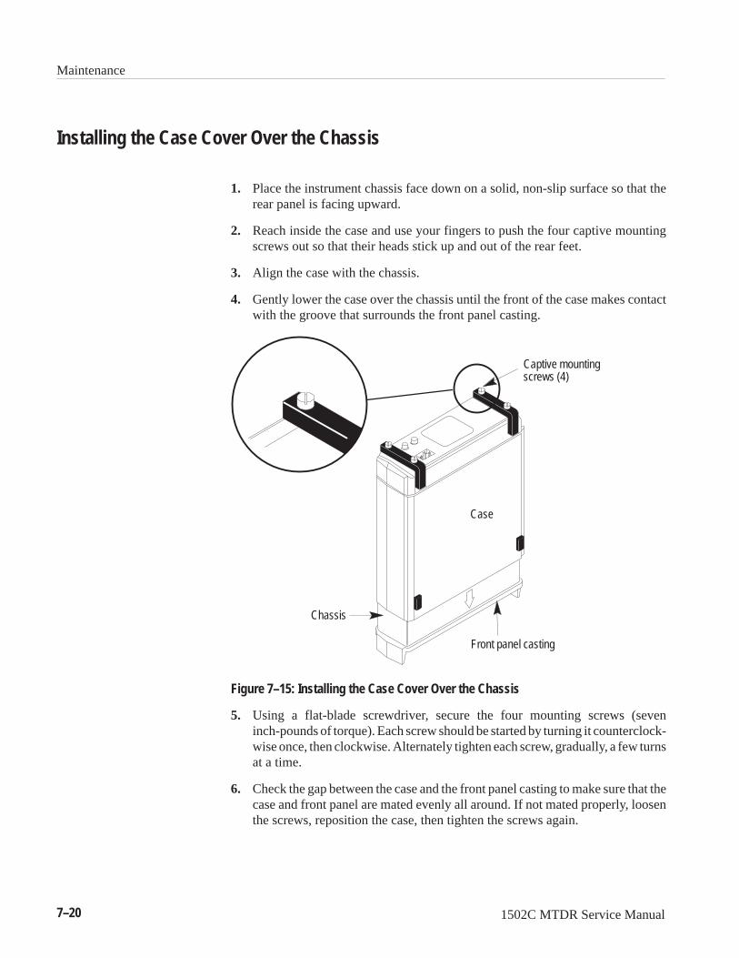
Maintenance
7–20 1502C MTDR Service Manual
Installing the Case Cover Over the Chassis
1. Place the instrument chassis face down on a solid, non-slip surface so that therear panel is facing upward.
2. Reach inside the case and use your fingers to push the four captive mountingscrews out so that their heads stick up and out of the rear feet.
3. Align the case with the chassis.
4. Gently lower the case over the chassis until the front of the case makes contactwith the groove that surrounds the front panel casting.
Captive mountingscrews (4)
Case
Chassis
Front panel casting
Figure 7–15: Installing the Case Cover Over the Chassis
5. Using a flat-blade screwdriver, secure the four mounting screws (seveninch-pounds of torque). Each screw should be started by turning it counterclock-wise once, then clockwise. Alternately tighten each screw, gradually, a few turnsat a time.
6. Check the gap between the case and the front panel casting to make sure that thecase and front panel are mated evenly all around. If not mated properly, loosenthe screws, reposition the case, then tighten the screws again.

1502C MTDR Service Manual8–1
Replaceable Electrical Parts
Parts Ordering InformationReplacement parts are available from your Tektronix field office or representative.When ordering parts, include the part number plus instrument type, serial number,and modification number (if applicable).
If a part is replaced with a new or improved part, your Tektronix representative willcontact you regarding any change in part number.
A list of assemblies is found at the beginning of the replaceable electrical parts list.Assemblies are listed in numerical order. When the complete component numberof a part is known, this list identifies the assembly in which the part is located.
The manufacturer code number-to-manufacturer cross index provides codes,names, and addresses of manufacturers of components listed in the replaceableelectrical parts list.
Abbreviations conform to ANSI standard Y1.1.
(Column 1 of electrical parts list)
A numbering method is used to identify assemblies, subassemblies, and parts. Anexample of this numbering method and typical expansions is as follows:
A23A2R1234 = A23 A2 R1234↓ ↓ ↓
Assembly Subassembly CircuitNumber Number Number
Read: resistor 1234 of subassembly 2 of assy 23.
Only circuit numbers appear on the schematics and circuit board illustrations. Eachschematic and illustration is marked with its assembly number. Assembly numbersare also marked on the mechanical exploded view located in the replaceablemechanical parts list. A component number is obtained by adding the assemblynumber prefix to the circuit number.
This parts list is arranged by assemblies in numerical sequence (e.g., assembly A1with its subassemblies and parts precedes A2 with its subassemblies and parts).
Chassis-mounted parts have no assembly number prefix and are illustrated at theend of the replaceable mechanical parts list.
List of Assemblies
Mfr. CodeNumber-to-Manufacturer
Cross Index
Abbreviations
Component Number

Replaceable Electrical Parts
8–2 1502C MTDR Service Manual
(Column 2)
This column lists the part number used when ordering a replacement part fromTektronix.
(Columns 3 and 4)
Column 3 lists the serial number of the first instrument or the suffix number of thecircuit board in which the part was used.
Column 4 lists the serial number of the last instrument or the suffix number of thecircuit board in which the part was used. No entry indicates that the part is used inall instruments.
(Column 5)
In this parts list, the item name is separated from its description by a colon (:).Because of space limitations, the item name may appear to be incomplete. Forfurther item name identification, refer to the U.S. Federal Cataloging Handbook,H6–1.
(Column 6)
This column lists the code number of the manufacturer of the part.
(Column 7)
This column lists the manufacturer’s part number.
Tektronix Part No.
Serial/Model No.
Name and Description
Mfg. Code
Mfg. Part Number

Replaceable Electrical Parts
1502C MTDR Service Manual8–3
Manufacturers Cross Index
Mfr.Code Manufacturer Address City, State, Zip Code
TK2460 VIKAY AMERICA INC 195 WEST MAIN ST SUITE 19 AVON CT 06001
TK2582 TUFF CAT USA LLC 814 N HAYDEN MEADOWS DRIVE PORTLAND, OR 97217
TK6181 IMC PLASTICS INC 19400 SW TETON AVE TUALATIN, OR 97062
01002 GENERAL ELECTRIC CO 381 UPPER BROADWAY FORT EDWARDS NY 12828–1021
01121 ALLEN–BRADLEY CO 1201 S 2ND ST MILWAUKEE WI 53204–2410
01295 TEXAS INSTRUMENTS INC 13500 N CENTRAL EXPY PO BOX 655303 DALLAS TX 75262–5303
01686 RCL ELECTRONICS/SHALLCROSS INC 195 MCGREGOR ST MANCHESTER NH 03102–3731
02111 SPECTROL ELECTRONICS CORP 4051 GREYSTONE DRIVE ONTARIO CA 91761
04222 AVX CERAMICS 19TH AVE SOUTH PO BOX 867 MYRTLE BEACH SC 29577
04426 ITW SWITCHES 6615 W IRVING PARK RD CHICAGO IL 60634–2410
04713 MOTOROLA INC 5005 E MCDOWELL RD PHOENIX AZ 85008–4229
049S6 FUJITSU COMPUTER PRODUCTS OFAMERICA INC
2904 ORCHARD PARKWAY SAN JOSE, CA 95134–2009
060D9 UNITREK CORPORATION 3000 COLUMBIA HOUSE BLDG SUITE 120 VANCOUVER WA 98661
07716 IRC, INC 2850 MT PLEASANT AVE BURLINGTON IA 52601
09353 C AND K COMPONENTS INC 15 RIVERDALE AVE NEWTON MA 02158–1057
09922 FRAMATOME CONNECTORS USA INC 51 RICHARDS AVE PO BOX 5200 NORWALK CT 06856
0B0A9 DALLAS SEMICONDUCTOR CORP 4350 BELTWOOD PKWY SOUTH DALLAS TX 75244
0GV52 SCHAFFNER EMC INC 9–B FADEM ROAD SPRINGFIELD NJ 07081
0H1N5 UNITED CHEMI–CON INC 9801 W HIGGINS RD ROSEMONT, IL 60018–4771
0JR03 ZMAN MAGNETICS INC 7633 S 180th KENT WA 98032
0JR04 TOSHIBA AMERICA INC 9775 TOLEDO WAY IRVINE CA 92718
0YZS5 HANTRONIX INCORPORATED 10080 BUBB ROAD CUPERTINO, CA 95014–4132
10392 GENERAL STAPLE CO INC 59–12 37TH ST WOODSIDE NY 11377–2523
12697 CLAROSTAT MFG CO INC 12055 ROJAS DRIVE SUITE K EL PASE TX 79936
12954 MICROSEMI CORP – SCOTTSDALE 8700 E THOMAS RD PO BOX 1390 SCOTTSDALE AZ 85252
12969 MICROSEMI CORP – WATERTOWN 530 PLEASANT STREET WATERTOWN MA 02172
13409 SENSITRON SEMICONDUCTOR 221 W INDUSTRY COURT DEER PARK NY 11729–4605
14433 ITT SEMICONDUCTORS DIV 2540 N 1ST ST SUITE 203 SAN JOSE CA 95131–1016
14552 MICROSEMI CORP 2830 S FAIRVIEW ST SANTA ANA CA 92704–5948
14936 GENERAL INSTRUMENT CORP 600 W JOHN ST HICKSVILLE NY 11802–0709
16546 PHILIPS COMPONENTS 4561 COLORADO BLVD LOS ANGELES CA 90039–1103
17856 TEMIC NORTH AMERICA SILICONIX 2201 LAURELWOOD RD SANTA CLARA CA 95054–1516
18324 PHILIPS SEMICONDUCTORS 830 STEWARD RD SUNNYVALE CA 94088
18796 MURATA ERIE NORTH AMERICAN INC 1900 W COLLEGE AVE STATE COLLEGE PA 16801–2723
19701 PHILIPS COMPONENTS DISCRETE PRODUCT AIRPORT RD PO BOX 760 MINERAL WELLS TX 76067–0760
21845 SOLITRON DEVICES INC 3301 ELECTRONICS WAY WEST PALM BEACH FL 33407
21847 FEI MICROWAVE INC 825 STEWART DR SUNNYVALE CA 94086–4514
22526 BERG ELECTRONICS 825 OLD TRAIL RD ETTERS PA 17319

Replaceable Electrical Parts
8–4 1502C MTDR Service Manual
Manufacturers Cross Index (Cont.)
Mfr.Code City, State, Zip CodeAddressManufacturer24165 SPRAGUE ELECTRIC CO 267 LOWELL ROAD HUDSON NH 03051
24355 ANALOG DEVICES INC 1 TECHNOLOGY DR NORWOOD MA 02062
26003 MARTEK POWER MDI 4115 SPENCER STREET TORRANCE, CA 90503–2489
27014 NATIONAL SEMICONDUCTOR CORP 2900 SEMICONDUCTOR DR SANTA CLARA CA 95051–0606
31433 KEMET ELECTRONICS CORP PO BOX 5928 GREENVILLE SC 29606
32997 BOURNS INC TRIMPOT DIV 1200 COLUMBIA AVE RIVERSIDE CA 92507–2114
34333 LINFINITY MICROELECTRONICS 11861 WESTERN AVE GARDEN GROVE CA 92641
34371 HARRIS CORP PO BOX 883 MELBOURNE FL 32902–0883
34649 INTEL CORP 3065 BOWERS AVE PO BOX 58130 SANTA CLARA CA 95051
4T165 NEC ELECTRONICS, INC. 2880 SCOTT BLVDPO BOX 58062
SANTA CLARA, CA 95052–8062
50434 HEWLETT–PACKARD CO 370 W TRIMBLE RD SAN JOSE CA 95131–1008
53387 3M COMPANY 3M AUSTIN CENTER AUSTIN TX 78769–2963
54937 DEYOUNG MANUFACTURING INC 12920 NE 125TH WAY KIRKLAND WA 98034–7716
55680 NICHICON /AMERICA/ CORP 927 E STATE PKY SCHAUMBURG IL 60195–4526
56637 RCD COMPONENTS INC 520 E INDUSTRIAL PARK DR MANCHESTER NH 03103
56845 DALE ELECTRONICS INC 2300 RIVERSIDE BLVD PO BOX 74 NORFOLK NE 68701–2242
56866 QUALITY THERMISTOR INC 2096 SOUTH COLE RD SUITE 7 BOISE ID 83705
57668 ROHM CORP 15375 BARRANCA PARKWAY SUITE B207 IRVINE CA 92718
58050 TEKA PRODUCTS INC 45 SALEM ST PROVIDENCE RI 02907
61935 SCHURTER INC 1016 CLEGG COURT PETALUMA CA 94952–1152
62643 UNITED CHEMICON INC 9801 W HIGGINS RD ROSEMONT IL 60018–4771
63312 ENDICOTT RESEARCH GROUP INC 2601 WAYNE ST PO BOX 269 ENDICOTT NY 13760–3272
64537 KDI/TRIANGLE ELECTRONICS 60 S JEFFERSON RD WHIPPANY NJ 07981
71400 BUSSMAN 114 OLD STATE RD PO BOX 14460 ST LOUIS MO 63178
71590 CGE SWITCHES – USA PO BOX 1587 FORT DODGE IA 50501
75042 IRC ELECTRONIC COMPONENTS 401 N BROAD ST PHILADELPHIA PA 19108–1001
75378 CTS KNIGHTS INC 400 REIMANN AVE SANDWICH IL 60548–1846
75915 LITTLEFUSE TRACOR INC 800 E NORTHWEST HWY DES PLAINES, IL 60016–3049
80009 TEKTRONIX INC 14150 SW KARL BRAUN DR PO BOX 500 BEAVERTON OR 97077–0001
81073 GRAYHILL INC 561 HILLGROVE AVE PO BOX 10373 LA GRANGE IL 60525–5914
81855 EAGLE–PICHER INDUSTRIES INC COUPLES DEPT C – PORTER STS PO BOX 47 JOPLIN MO 64801
91637 DALE ELECTRONICS INC 2064 12TH AVE PO BOX 609 COLUMBUS NE 68601–3632
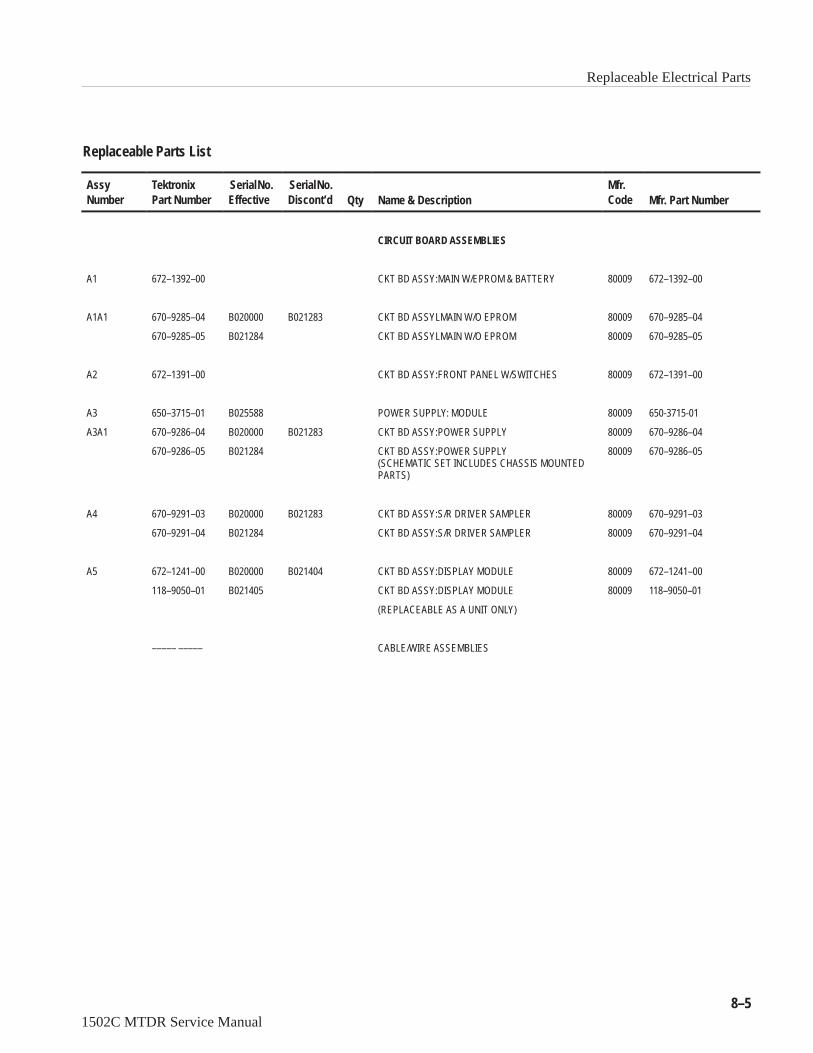
Replaceable Electrical Parts
1502C MTDR Service Manual8–5
Replaceable Parts List
AssyNumber
TektronixPart Number
Serial No.Effective
Serial No.Discont’d Qty Name & Description
Mfr.Code Mfr. Part Number
CIRCUIT BOARD ASSEMBLIES
A1 672–1392–00 CKT BD ASSY:MAIN W/EPROM & BATTERY 80009 672–1392–00
A1A1 670–9285–04 B020000 B021283 CKT BD ASSYLMAIN W/O EPROM 80009 670–9285–04
670–9285–05 B021284 CKT BD ASSYLMAIN W/O EPROM 80009 670–9285–05
A2 672–1391–00 CKT BD ASSY:FRONT PANEL W/SWITCHES 80009 672–1391–00
A3 650–3715–01 B025588 POWER SUPPLY: MODULE 80009 650-3715-01
A3A1 670–9286–04 B020000 B021283 CKT BD ASSY:POWER SUPPLY 80009 670–9286–04
670–9286–05 B021284 CKT BD ASSY:POWER SUPPLY(SCHEMATIC SET INCLUDES CHASSIS MOUNTEDPARTS)
80009 670–9286–05
A4 670–9291–03 B020000 B021283 CKT BD ASSY:S/R DRIVER SAMPLER 80009 670–9291–03
670–9291–04 B021284 CKT BD ASSY:S/R DRIVER SAMPLER 80009 670–9291–04
A5 672–1241–00 B020000 B021404 CKT BD ASSY:DISPLAY MODULE 80009 672–1241–00
118–9050–01 B021405 CKT BD ASSY:DISPLAY MODULE 80009 118–9050–01
(REPLACEABLE AS A UNIT ONLY)
––––– ––––– CABLE/WIRE ASSEMBLIES

Replaceable Electrical Parts
8–6 1502C MTDR Service Manual
Replaceable Parts List (Cont.)
AssyNumber Mfr. Part Number
Mfr.CodeName & DescriptionQty
Serial No.Discont’d
Serial No.Effective
TektronixPart Number
A1 672–1392–XX CKT BD ASSY:MAIN BD W/EPROM & BATTERY
A1U2020 160–9010–00 IC,MEMORY:EPROM,PROG 80009 160–9010–00
A1BT1010 146–0049–00 BATTERY,STORAGE:3.5V,750MAH SFTY CONT 81855 LTC–7P
A1A1 670–9285–XX CIRCUIT BD ASSY:MAIN
A1A1C1010 281–0925–01 CAP,FXD,CER DI:MLC,0.22UF,20%,50V,Z5U 31433 C114C224M5Y5CA
A1A1C1011 281–0925–01 CAP,FXD,CER DI:MLC,0.22UF,20%,50V,Z5U 31433 C114C224M5Y5CA
A1A1C1020 281–0925–01 CAP,FXD,CER DI:MLC,0.22UF,20%,50V,Z5U 31433 C114C224M5Y5CA
A1A1C1021 281–0925–01 CAP,FXD,CER DI:MLC,0.22UF,20%,50V,Z5U 31433 C114C224M5Y5CA
A1A1C1022 283–0359–01 CAP,FXD,CER DI:1000PF,5%,200V SQ 31433 C322C102J2G5CA
A1A1C1023 283–0359–01 CAP,FXD,CER DI:1000PF,5%,200V SQ 31433 C322C102J2G5CA
A1A1C1024 283–0359–01 CAP,FXD,CER DI:1000PF,5%,200V SQ 31433 C322C102J2G5CA
A1A1C1030 283–0190–00 CAP,FXD,CER DI:0.47UF,5%,50V SQ 04222 SR305C474JAA
A1A1C1031 281–0925–01 CAP,FXD,CER DI:MLC,0.22UF,20%,50V,Z5U 31433 C114C224M5Y5CA
A1A1C1032 283–0359–01 CAP,FXD,CER DI:1000PF,5%,200V SQ 31433 C322C102J2G5CA
A1A1C1040 281–0925–01 CAP,FXD,CER DI:MLC,0.22UF,20%,50V,Z5U 31433 C114C224M5Y5CA
A1A1C1041 281–0925–01 CAP,FXD,CER DI:MLC,0.22UF,20%,50V,Z5U 31433 C114C224M5Y5CA
A1A1C1042 290–1087–00 CAP,FXD,ELCTLT:100UF,25V,AXIAL 62643 KME35T101M8X16LL
A1A1C1043 281–0925–01 CAP,FXD,CER DI:MLC,0.22UF,20%,50V,Z5U 31433 C114C224M5Y5CA
A1A1C2010 281–0925–01 CAP,FXD,CER DI:MLC,0.22UF,20%,50V,Z5U 31433 C114C224M5Y5CA
A1A1C2011 290–0748–00 CAP,FXD,ELCTLT:10UF,+50–20%,25W VDC 55680 TVX1E100MAA1LS
A1A1C2012 281–0925–01 CAP,FXD,CER DI:MLC,0.22UF,20%,50V,Z5U 31433 C114C224M5Y5CA
A1A1C2013 281–0925–01 CAP,FXD,CER DI:MLC,0.22UF,20%,50V,Z5U 31433 C114C224M5Y5CA
A1A1C2014 281–0925–01 CAP,FXD,CER DI:MLC,0.22UF,20%,50V,Z5U 31433 C114C224M5Y5CA
A1A1C2015 283–0111–04 CAP,FXD,CER DI:0.1UF,20%,50V SQ 04222 SR595C104MAAAP1
A1A1C2016 283–0238–00 CAP,FXD,CER DI:0.01UF,10%,50V SQ 04222 SR155C103KAA
A1A1C2020 281–0925–01 CAP,FXD,CER DI:MLC,0.22UF,20%,50V,Z5U 31433 C114C224M5Y5CA
A1A1C2021 281–0925–01 CAP,FXD,CER DI:MLC,0.22UF,20%,50V,Z5U 31433 C114C224M5Y5CA
A1A1C2030 281–0925–01 CAP,FXD,CER DI:MLC,0.22UF,20%,50V,Z5U 31433 C114C224M5Y5CA
A1A1C2031 281–0925–01 CAP,FXD,CER DI:MLC,0.22UF,20%,50V,Z5U 31433 C114C224M5Y5CA
A1A1C2032 281–0925–01 CAP,FXD,CER DI:MLC,0.22UF,20%,50V,Z5U 31433 C114C224M5Y5CA
A1A1C2033 281–0925–01 CAP,FXD,CER DI:MLC,0.22UF,20%,50V,Z5U 31433 C114C224M5Y5CA

Replaceable Electrical Parts
1502C MTDR Service Manual8–7
Replaceable Parts List (Cont.)
AssyNumber Mfr. Part Number
Mfr.CodeName & DescriptionQty
Serial No.Discont’d
Serial No.Effective
TektronixPart Number
A1A1C2034 281–0925–01 CAP,FXD,CER DI:MLC,0.22UF,20%,50V,Z5U 31433 C114C224M5Y5CA
A1A1C2035 281–0925–01 CAP,FXD,CER DI:MLC,0.22UF,20%,50V,Z5U 31433 C114C224M5Y5CA
A1A1C2036 281–0925–01 CAP,FXD,CER DI:MLC,0.22UF,20%,50V,Z5U 31433 C114C224M5Y5CA
A1A1C2037 281–0925–01 CAP,FXD,CER DI:MLC,0.22UF,20%,50V,Z5U 31433 C114C224M5Y5CA
A1A1C2038 281–0925–01 CAP,FXD,CER DI:MLC,0.22UF,20%,50V,Z5U 31433 C114C224M5Y5CA
A1A1C2039 283–0067–00 CAP,FXD,CER DI:0.001UF,10%,200V 18796 DD09B10 Y5F 102K 200V
A1A1C2040 283–0059–02 CAP,FXD,CER DI:1UF,20%,50V 04222 SR305C105MAATRSTDII
A1A1C2041 283–0059–02 CAP,FXD,CER DI:1UF,20%,50V 04222 SR305C105MAATRSTDII
A1A1C2042 281–0925–01 CAP,FXD,CER DI:MLC,0.22UF,20%,50V,Z5U 31433 C114C224M5Y5CA
A1A1C2043 283–0238–00 CAP,FXD,CER DI:0.01UF,10%,50V SQ 04222 SR155C103KAA
A1A1C2044 281–0925–01 CAP,FXD,CER DI:MLC,0.22UF,20%,50V,Z5U 31433 C114C224M5Y5CA
A1A1C2045 281–0272–00 CAP,FXD,CER DI:0.1UF,10%,50V 04222 SA115C104KAA
A1A1C2046 283–0067–00 CAP,FXD,CER DI:0.001UF,10%,200V 18796 DD09B10 Y5F 102K 200V
A1A1C3020 281–0925–01 CAP,FXD,CER DI:MLC,0.22UF,20%,50V,Z5U 31433 C114C224M5Y5CA
A1A1C3021 281–0925–01 CAP,FXD,CER DI:MLC,0.22UF,20%,50V,Z5U 31433 C114C224M5Y5CA
A1A1C3022 281–0925–01 CAP,FXD,CER DI:MLC,0.22UF,20%,50V,Z5U 31433 C114C224M5Y5CA
A1A1C3023 281–0925–01 CAP,FXD,CER DI:MLC,0.22UF,20%,50V,Z5U 31433 C114C224M5Y5CA
A1A1C3030 283–0181–00 CAP,FXD,CER DI:1.8PF,+/–0.1%,100V SQ 24165 5024E0200RD221K
A1A1C3040 283–0107–00 CAP,FXD,CER DI:51PF,5%,200V SQ 04222 SR202A510JAA
A1A1C3041 283–0167–00 CAP,FXD,CER DI:0.1UF,10%,100V SQ 04222 SR211C104KAA
A1A1C3042 283–0108–02 CAP,FXD,CER DI:220PF,10%,200V SQ 04222 SR075A221KAAAP1
A1A1C3043 283–0330–00 CAP,FXD,CER DI:100PF,5%,50V SQ 16546 CN15C101J
A1A1C3044 283–0359–01 CAP,FXD,CER DI:1000PF,5%,200V SQ 31433 C322C102J2G5CA
A1A1C3045 281–0925–01 CAP,FXD,CER DI:MLC,0.22UF,20%,50V,Z5U 31433 C114C224M5Y5CA
A1A1C3046 281–0925–01 CAP,FXD,CER DI:MLC,0.22UF,20%,50V,Z5U 31433 C114C224M5Y5CA
A1A1C3047 283–0181–00 CAP,FXD,CER DI:1.8PF,+/–0.1%,100V SQ 24165 5024E0200RD221K
A1A1C3048 283–0359–01 CAP,FXD,CER DI:1000PF,5%,200V SQ 31433 C322C102J2G5CA
A1A1C4020 281–0925–01 CAP,FXD,CER DI:MLC,0.22UF,20%,50V,Z5U 31433 C114C224M5Y5CA
A1A1C4021 283–0359–01 CAP,FXD,CER DI:1000PF,5%,200V SQ 31433 C322C102J2G5CA
A1A1C4022 285–1241–00 CAP,FXD,PLASTIC:0.22UF,10%,100V 12954 B32571.22/10/100
A1A1C4030 281–0925–01 CAP,FXD,CER DI:MLC,0.22UF,20%,50V,Z5U 31433 C114C224M5Y5CA
A1A1C4040 281–0813–00 CAP,FXD,CER DI:MLC,0.04UF,20%,50V 04222 SA105E473MAA
A1A1C4041 290–0748–00 CAP,FXD,ELCTLT:10UF,+50–20%,25W VDC 62643 CEUST1E100
A1A1C5010 283–0330–00 CAP,FXD,CER DI:100PF,5%,50V SQ 16546 CN15C101J
A1A1C5020 283–0359–01 CAP,FXD,CER DI:1000PF,5%,200V SQ 31433 C322C102J2G5CA
A1A1C5021 283–0359–01 CAP,FXD,CER DI:1000PF,5%,200V SQ 31433 C322C102J2G5CA
A1A1C5022 281–0925–01 CAP,FXD,CER DI:MLC,0.22UF,20%,50V,Z5U 31433 C114C224M5Y5CA
A1A1C5023 283–0359–01 CAP,FXD,CER DI:1000PF,5%,200V SQ 31433 C322C102J2G5CA

Replaceable Electrical Parts
8–8 1502C MTDR Service Manual
Replaceable Parts List (Cont.)
AssyNumber Mfr. Part Number
Mfr.CodeName & DescriptionQty
Serial No.Discont’d
Serial No.Effective
TektronixPart Number
A1A1C5024 283–0177–00 CAP,FXD,CER DI:1UF,+80–20%,25V 04222 SR305E105ZAA
A1A1C5025 283–0177–00 CAP,FXD,CER DI:1UF,+80–20%,25V 04222 SR305E105ZAA
A1A1C5030 281–0813–00 CAP,FXD,CER DI:MLC,0.04UF,20%,50V 04222 SA105E473MAA
A1A1C5031 281–0813–00 CAP,FXD,CER DI:MLC,0.04UF,20%,50V 04222 SA105E473MAA
A1A1C5032 281–0798–00 CAP,FXD,CER DI:51PF,1%,100V TUBULAR,MI 04222 SA101A510GAA
A1A1C5033 283–0330–00 CAP,FXD,CER DI:100PF,5%,50V SQ 16546 CN15C101J
A1A1C5040 283–0330–00 CAP,FXD,CER DI:100PF,5%,50V SQ 16546 CN15C101J
A1A1C5041 281–0925–01 CAP,FXD,CER DI:MLC,0.22UF,20%,50V,Z5U 31433 C114C224M5Y5CA
A1A1C5042 281–0925–01 CAP,FXD,CER DI:MLC,0.22UF,20%,50V,Z5U 31433 C114C224M5Y5CA
A1A1C6030 281–0925–01 CAP,FXD,CER DI:MLC,0.22UF,20%,50V,Z5U 31433 C114C224M5Y5CA
A1A1C6031 283–0177–00 CAP,FXD,CER DI:1UF,+80–20%,25V 04222 SR305E105ZAA
A1A1C6032 281–0925–01 CAP,FXD,CER DI:MLC,0.22UF,20%,50V,Z5U 31433 C114C224M5Y5CA
A1A1C7010 283–0111–04 CAP,FXD,CER DI:0.1UF,20%,50V SQ 04222 SR595C104MAAAP1
A1A1C7020 281–0813–00 CAP,FXD,CER DI:MLC,0.04UF,20%,50V 04222 SA105E473MAA
A1A1C7021 281–0925–01 CAP,FXD,CER DI:MLC,0.22UF,20%,50V,Z5U 31433 C114C224M5Y5CA
A1A1C7022 283–0359–01 CAP,FXD,CER DI:1000PF,5%,200V SQ 31433 C322C102J2G5CA
A1A1C7023 283–0177–00 CAP,FXD,CER DI:1UF,+80–20%,25V 04222 SR305E105ZAA
A1A1C7030 283–0059–02 CAP,FXD,CER DI:1UF,20%,50V 04222 SR305C105MAATRSTDII
A1A1C7040 283–0330–00 CAP,FXD,CER DI:100PF,5%,50V SQ 16546 CN15C101J
A1A1C7041 281–0925–01 CAP,FXD,CER DI:MLC,0.22UF,20%,50V,Z5U 31433 C114C224M5Y5CA
A1A1C7042 281–0925–01 CAP,FXD,CER DI:MLC,0.22UF,20%,50V,Z5U 31433 C114C224M5Y5CA
A1A1C7043 290–0748–00 CAP,FXD,ELCTLT:10UF,+50–20%,25W VDC 62643 CEUST1E100
A1A1C8010 281–0925–01 CAP,FXD,CER DI:MLC,0.22UF,20%,50V,Z5U 31433 C114C224M5Y5CA
A1A1C8020 283–0010–00 CAP,FXD,CER DI:0.05UF,+80–20%,50V SQ 04222 SR305E503ZAA
A1A1C8021 281–0798–00 CAP,FXD,CER DI:51PF,1%,100V TUBULAR,MI 04222 SA101A510GAA
A1A1C8022 283–0330–00 CAP,FXD,CER DI:100PF,5%,50V SQ 16546 CN15C101J
A1A1C8023 281–0925–01 CAP,FXD,CER DI:MLC,0.22UF,20%,50V,Z5U 31433 C114C224M5Y5CA
A1A1C8024 283–0348–00 CAP,FXD,CER DI:0.5PF,+/–0.1PF,100V 31433 C312C109D1G5EA
A1A1C8040 283–0156–00 CAP,FXD,CER DI:1000PF,+80–20%,200V SQ 04222 SR152E102ZAA
A1A1C9010 283–0111–04 CAP,FXD,CER DI:0.1UF,20%,50V SQ 04222 SR595C104MAAAP1
A1A1C9011 281–0813–00 CAP,FXD,CER DI:MLC,0.047UF,20%,50V 04222 SA105E473MAA
A1A1C9020 283–0359–01 CAP,FXD,CER DI:1000PF,5%,200V SQ 31433 C322C102J2G5CA
A1A1C9021 281–0925–01 CAP,FXD,CER DI:MLC,0.22UF,20%,50V,Z5U 31433 C114C224M5Y5CA
A1A1C9022 281–0813–00 CAP,FXD,CER DI:MLC,0.04UF,20%,50V 04222 SA105E473MAA
A1A1C9023 281–0925–01 CAP,FXD,CER DI:MLC,0.22UF,20%,50V,Z5U 31433 C114C224M5Y5CA
A1A1C9024 281–0813–00 CAP,FXD,CER DI:MLC,0.04UF,20%,50V 04222 SA105E473MAA
A1A1C9025 281–0925–01 CAP,FXD,CER DI:MLC,0.22UF,20%,50V,Z5U 31433 C114C224M5Y5CA
A1A1C9030 281–0925–01 CAP,FXD,CER DI:MLC,0.22UF,20%,50V,Z5U 31433 C114C224M5Y5CA

Replaceable Electrical Parts
1502C MTDR Service Manual8–9
Replaceable Parts List (Cont.)
AssyNumber Mfr. Part Number
Mfr.CodeName & DescriptionQty
Serial No.Discont’d
Serial No.Effective
TektronixPart Number
A1A1C9031 290–0748–00 CAP,FXD,ELCTLT:10UF,+50–20%,25W VDC 62643 CEUST1E100
A1A1C9032 283–0359–01 CAP,FXD,CER DI:1000PF,5%,200V SQ 31433 C322C102J2G5CA
A1A1C9033 283–0359–01 CAP,FXD,CER DI:1000PF,5%,200V SQ 31433 C322C102J2G5CA
A1A1C9034 281–0925–01 CAP,FXD,CER DI:MLC,0.22UF,20%,50V,Z5U 31433 C114C224M5Y5CA
A1A1C9035 290–0748–00 CAP,FXD,ELCTLT:10UF,+50–20%,25W VDC 62643 CEUST1E100
A1A1CR1020 152–0322–00 DIODE DVC,DI:SCHOTTKY,SI,15V,1.2PF 21847 A2X600
A1A1CR1021 152–0322–00 DIODE DVC,DI:SCHOTTKY,SI,15V,1.2PF 21847 A2X600
A1A1CR1022 152–0322–00 DIODE DVC,DI:SCHOTTKY,SI,15V,1.2PF 21847 A2X600
A1A1CR1023 152–0322–00 DIODE DVC,DI:SCHOTTKY,SI,15V,1.2PF 21847 A2X600
A1A1CR3031 152–0322–00 DIODE DVC,DI:SCHOTTKY,SI,15V,1.2PF 21847 A2X600
A1A1CR4030 152–0141–02 DIODE,SIG:ULTRA FAST;40V,150MA,4NS,2PF 01295 1N4152R
A1A1CR4031 152–0322–00 DIODE DVC,DI:SCHOTTKY,SI,15V,1.2PF 21847 A2X600
A1A1CR4032 152–0725–00 DIODE DVC,DI:SI,SCHOTTKY,20V,1.2PF 21847 A2X1582
A1A1CR5030 152–0725–00 DIODE DVC,DI:SI,SCHOTTKY,20V,1.2PF 21847 A2X1582
A1A1CR5040 152–0322–00 DIODE DVC,DI:SCHOTTKY,SI,15V,1.2PF 21847 A2X600
A1A1CR8020 152–0322–00 DIODE DVC,DI:SCHOTTKY,SI,15V,1.2PF 21847 A2X600
A1A1CR9010 152–0322–00 DIODE DVC,DI:SCHOTTKY,SI,15V,1.2PF 21847 A2X600
A1A1J2010 131–3361–00 CONN,HDR:PCB,MALE,RTANG,2 X 13,0.1 CTR 53387 3593–5002
A1A1J5040 131–4183–00 CONN,HDR:PCB,MALE,STR,2 X 7,0.1 CTR 53387 3598–6002
A1A1J9010 131–3359–00 CONN,HDR:PCB,MALE,RTANG,2 X 10,0.1 CTR 53387 3592–5002
A1A1L5030 120–1606–00 XFMR,RF:INDUCTOR 86–10 0JR03 120–1606–00
A1A1L5040 108–0509–01 COIL,RF:FIXED,2.45UH +/–10%,AXIAL LEAD 0JR03 108–0509–01
A1A1Q1010 151–1176–00 XSTR,PWR:MOS,P–CH;100V,1.0A,0.6 OHM 04713 IRFD9120
A1A1Q1020 151–0190–00 XSTR,SIG:BIPOLAR,NPN;40V,200MA,300MHZ,AMP 01295 SKA3703
A1A1Q1021 151–0188–00 XSTR,SIG:BIPOLAR,PNP;40V,200MA,250MHZ,AMP 34371 X39H3162
A1A1Q1030 151–0190–00 XSTR,SIG:BIPOLAR,NPN;40V,200MA,300MHZ,AMP 01295 SKA3703
A1A1Q1031 151–0188–00 XSTR,SIG:BIPOLAR,PNP;40V,200MA,250MHZ,AMP 34371 X39H3162
A1A1Q2011 151–1176–00 XSTR,PWR:MOS,P–CH;100V,1.0A,0.6 OHM 04713 IRFD9120
A1A1Q2012 151–1176–00 XSTR,PWR:MOS,P–CH;100V,1.0A,0.6 OHM 04713 IRFD9120
A1A1Q3030 151–0276–01 XSTR,SIG:BIPOLAR,PNP;50V,50MA,40MHZ,AMP 04713 2N5087RLRP
A1A1Q4030 151–1078–00 XSTR,SIG:JFET,N–CH;3.5V,75MA,90 OHM;TO–92 04713 SPF3040
A1A1Q4031 151–0441–00 B020000 B023865 XSTR,SIG:BIPOLAR,NPN,25V,50MA,650MHZ,TO–92 04713 2N3839
151–0711–00 B023866 XSTR,SIG:BIPOLAR,NPN,25V,50MA,650MHZ,TO–92 04713 MPSH10
A1A1Q4040 151–0271–00 XSTR,SIG:BIPOLAR,PNP;15V,30MA,2.0GHZ,AMP 01295 SKA4504

Replaceable Electrical Parts
8–10 1502C MTDR Service Manual
Replaceable Parts List (Cont.)
AssyNumber Mfr. Part Number
Mfr.CodeName & DescriptionQty
Serial No.Discont’d
Serial No.Effective
TektronixPart Number
A1A1Q5020 151–0308–00 XSTR,SIG:BIPOLAR,NPN;45V,30MA,60MHZ,AMP 04713 2N2918
A1A1Q5030 151–0441–00 B020000 B023865 XSTR,SIG:BIPOLAR,NPN;15V,40MA,1.0GHZ,AMP 04713 2N3839
151–0711–00 B023866 XSTR,SIG:BIPOLAR,NPN,25V,50MA,650MHZ,TO–92 04713 MPSH10
A1A1Q5031 151–1012–00 XSTR,SIG:JFET,N–CH,6V,15MA,AMP 21845 F1585
A1A1Q5032 151–0261–00 XSTR,SIG:BIPOLAR,PNP;60V,50MA,100MHZ,AMP 04713 2N3810
A1A1Q6020 151–0271–00 XSTR,SIG:BIPOLAR,PNP;15V,30MA,2.0GHZ,AMP 01295 SKA4504
A1A1Q7020 151–0441–00 B020000 B023865 XSTR,SIG:BIPOLAR,NPN;15V,40MA,1.0GHZ,AMP 04713 2N3839
151–0711–00 B023866 XSTR,SIG:BIPOLAR,NPN,25V,50MA,650MHZ,TO–92 04713 MPSH10
A1A1Q7021 151–0139–00 XSTR,SIG:BIPOLAR,NPN;15V,50MA,600MHZ,AMP 04713 MD918
A1A1Q7030 151–0441–00 B020000 B023865 XSTR,SIG:BIPOLAR,NPN;15V,40MA,1.0GHZ,AMP 04713 2N3839
151–0711–00 B023866 XSTR,SIG:BIPOLAR,NPN,25V,50MA,650MHZ,TO–92 04713 MPSH10
A1A1Q8020 151–0139–00 XSTR,SIG:BIPOLAR,NPN;15V,50MA,600MHZ,AMP 04713 MD918
A1A1Q9010 151–0271–00 XSTR,SIG:BIPOLAR,PNP;15V,30MA,2.0GHZ,AMP 01295 SKA4504
A1A1Q9020 151–0308–00 XSTR,SIG:BIPOLAR,NPN;45V,30MA,60MHZ,AMP 04713 2N2918
A1A1Q9021 151–0271–00 XSTR,SIG:BIPOLAR,PNP;15V,30MA,2.0GHZ,AMP 01295 SKA4504
A1A1R1010 322–3162–00 RES,FXD:METAL FILM:475 OHM,1%,0.2W 57668 CRB20 FXE 475E
A1A1R1011 322–3289–00 RES,FXD:METAL FILM:10.0K OHM,1%,0.2W 57668 CRB20 FXE 10K0
A1A1R1012 322–3289–00 RES,FXD:METAL FILM:10.0K OHM,1%,0.2W 57668 CRB20 FXE 10K0
A1A1R1013 322–3289–00 RES,FXD:METAL FILM:10.0K OHM,1%,0.2W 57668 CRB20 FXE 10K0
A1A1R1014 322–3385–00 RES,FXD:METAL FILM:100K OHM,1%,0.2W 57668 CRB20 FXE 100K
A1A1R1015 322–3318–00 RES,FXD:METAL FILM:20.0K OHM,1%,0.2W 57668 CRB20 FXE 20K0
A1A1R1016 322–3097–00 RES,FXD:METAL FILM:100 OHM,1%,0.2W 57668 CRB20 FXE 100E
A1A1R1020 322–3289–00 RES,FXD:METAL FILM:10.0K OHM,1%,0.2W 57668 CRB20 FXE 10K0
A1A1R1021 322–3289–00 RES,FXD:METAL FILM:10.0K OHM,1%,0.2W 57668 CRB20 FXE 10K0
A1A1R1022 322–3289–00 RES,FXD:METAL FILM:10.0K OHM,1%,0.2W 57668 CRB20 FXE 10K0
A1A1R1023 322–3289–00 RES,FXD:METAL FILM:10.0K OHM,1%,0.2W 57668 CRB20 FXE 10K0
A1A1R1032 322–3437–00 RES,FXD,FILM:348K OHM,1%,0.2W 57668 CRB20 FXE 348K
A1A1R1033 307–0446–00 RES NTWK,FXD,FI:10K OHM,20%,(9)RES 01121 210A103
A1A1R1035 321–0756–00 RES,FXD,FILM:50K OHM,1%,0.125W 01121 ADVISE
A1A1R2010 322–3097–00 RES,FXD:METAL FILM:100 OHM,1%,0.2W 57668 CRB20 FXE 100E
A1A1R2011 322–3318–00 RES,FXD:METAL FILM:20.0K OHM,1%,0.2W 57668 CRB20 FXE 20K0
A1A1R2012 322–3385–00 RES,FXD:METAL FILM:100K OHM,1%,0.2W 57668 CRB20 FXE 100K
A1A1R2013 322–3385–00 RES,FXD:METAL FILM:100K OHM,1%,0.2W 57668 CRB20 FXE 100K
A1A1R2014 307–0446–00 RES NTWK,FXD,FI:10K OHM,20%,(9)RES 01121 210A103
A1A1R2015 307–0446–00 RES NTWK,FXD,FI:10K OHM,20%,(9)RES 01121 210A103
A1A1R2030 322–3239–00 RES,FXD,FILM:3.01K OHM,1%,0.2W 57668 CRB20 FXE 3K01
A1A1R2031 322–3239–00 RES,FXD,FILM:3.01K OHM,1%,0.2W 57668 CRB20 FXE 3K01

Replaceable Electrical Parts
1502C MTDR Service Manual8–11
Replaceable Parts List (Cont.)
AssyNumber Mfr. Part Number
Mfr.CodeName & DescriptionQty
Serial No.Discont’d
Serial No.Effective
TektronixPart Number
A1A1R2033 322–3293–00 RES,FXD:METAL FILM:11.0K OHM,1%,0.2W 57668 CRB20 FXE 11K0
A1A1R2034 311–0634–00 RES,VAR,NONWW:TRMR,500 OHM,0.5W CERMET 32997 3329H–L58–501
A1A1R2040 322–3139–00 RES,FXD:METAL FILM:274 OHM,1%,0.2W 57668 CRB20 FXE 274E
A1A1R2041 322–3134–00 RES,FXD,FILM:243 OHM,1%,0.2W 57668 CRB20 FXE243E
A1A1R2042 322–3134–00 RES,FXD,FILM:243 OHM,1%,0.2W 57668 CRB20 FXE243E
A1A1R2043 322–3126–00 RES,FXD,FILM:200 OHM,1%,0.2W 91637 CCF501G200R0F
A1A1R3010 322–3097–00 RES,FXD:METAL FILM:100 OHM,1%,0.2W 57668 CRB20 FXE 100E
A1A1R3020 322–3297–00 RES,FXD:METAL FILM:12.1K OHM,1%,0.2W 57668 CRB20 FXE 12K1
A1A1R3030 322–3097–00 RES,FXD:METAL FILM:100 OHM,1%,0.2W 57668 CRB20 FXE 100E
A1A1R3031 322–3356–00 RES,FXD,FILM:49.9K OHM,1%,0.2W 57668 CRB20 FXE 49K9
A1A1R3032 322–3327–00 RES,FXD,FILM:24.9K OHM,1%,0.2W 57668 CRB20 FXE 24K9
A1A1R3033 322–3165–00 RES,FXD,FILM:511 OHM,1%,0.2W 57668 CRB20 FXE 511E
A1A1R3034 322–3261–00 RES,FXD,FILM:5.11K OHM,1%,0.2W 91637 CCF50G5111FT
A1A1R3035 322–3289–00 RES,FXD:METAL FILM:10.0K OHM,1%,0.2W 57668 CRB20 FXE 10K0
A1A1R3036 322–3243–00 RES,FXD:METAL FILM:3.32K OHM,1%,0.2W 91637 CCF50–1–G33200F
A1A1R3037 322–3314–00 RES,FXD:METAL FILM:18.2K OHM,1%,0.2W 57668 CRB20 FXE 18K2
A1A1R3038 322–3306–00 RES,FXD:METAL FILM:15.0K OHM,1%,0.2W 57668 CRB20 FXE 15K0
A1A1R3039 322–3327–00 RES,FXD,FILM:24.9K OHM,1%,0.2W 57668 CRB20 FXE 24K9
A1A1R3040 322–3385–00 RES,FXD:METAL FILM:100K OHM,1%,0.2W 57668 CRB20 FXE 100K
A1A1R3041 322–3126–00 RES,FXD,FILM:200 OHM,1%,0.2W 91637 CCF501G200R0F
A1A1R3042 322–3173–00 RES,FXD,FILM:619 OHM,1%,0.2W 91637 CCF50–2F619R0F
A1A1R4020 322–3297–00 RES,FXD:METAL FILM:12.1K OHM,1%,0.2W 57668 CRB20 FXE 12K1
A1A1R4021 322–3261–00 RES,FXD,FILM:5.11K OHM,1%,0.2W 91637 CCF50G5111FT
A1A1R4022 322–3385–00 RES,FXD:METAL FILM:100K OHM,1%,0.2W 57668 CRB20 FXE 100K
A1A1R4023 322–3347–00 RES,FXD,FILM:40.2K OHM,1%,0.2W 91637 CCF50–2–G40201F
A1A1R4030 322–3126–00 RES,FXD,FILM:200 OHM,1%,0.2W 91637 CCF501G200R0F
A1A1R4031 322–3325–00 RES,FXD,FILM:23.7K OHM,1%,0.2W 57668 CRB20 FXE 23K7
A1A1R4032 322–3261–00 RES,FXD,FILM:5.11K OHM,1%,0.2W 91637 CCF50G5111FT
A1A1R4040 322–3281–00 RES,FXD:METAL FILM:8.25K OHM,1%,0.2W 57668 CRB20 FXE 8K25
A1A1R4041 322–3134–00 RES,FXD,FILM:243 OHM,1%,0.2W 57668 CRB20 FXE243E
A1A1R4042 322–3135–00 RES,FXD,FILM:249 OHM,1%,0.2W 57668 CRB20 FXE 249E
A1A1R4043 321–0136–00 RES,FXD,FILM:255 OHM,1%,0.125W 19701 5043ED255R0F
A1A1R4044 322–3137–00 RES,FXD,FILM:261 OHM,1%,0.2W 57668 CRB20 FXE 261E
A1A1R4045 322–3138–00 RES,FXD,FILM:267 OHM,1%,0.2W 57668 CRB20 FXE 267E
A1A1R4046 322–3139–00 RES,FXD:METAL FILM:274 OHM,1%,0.2W 57668 CRB20 FXE 274E
A1A1R4047 322–3141–00 RES,FXD,FILM:287 OHM,1%,0.2W 57668 CRB20 FXE 287E
A1A1R4048 322–3001–00 RES,FXD:METAL FILM:10 OHM,1%,0.2W 57668 CRB20 FXE10E0
A1A1R5020 322–3395–07 RES,FXD,FILM:127K OHM,1%,0.2W 57668 BZE127K

Replaceable Electrical Parts
8–12 1502C MTDR Service Manual
Replaceable Parts List (Cont.)
AssyNumber Mfr. Part Number
Mfr.CodeName & DescriptionQty
Serial No.Discont’d
Serial No.Effective
TektronixPart Number
A1A1R5021 322–3289–00 RES,FXD:METAL FILM:10.0K OHM,1%,0.2W 57668 CRB20 FXE 10K0
A1A1R5022 322–3337–00 RES,FXD,FILM:31.6K OHM,1%,0.2W 91637 CCF502G31601FT
A1A1R5023 322–3164–00 RES,FXD,FILM:499 OHM,1%,0.2W 57668 CRB20 FXE 499E
A1A1R5024 322–3001–00 RES,FXD:METAL FILM:10 OHM,1%,0.2W 57668 CRB20 FXE10E0
A1A1R5025 322–3001–00 RES,FXD:METAL FILM:10 OHM,1%,0.2W 57668 CRB20 FXE10E0
A1A1R5026 322–3068–00 RES,FXD:METAL FILM:49.9 OHM,0.1%,0.2W 57668 CRB20 FXE 49E9
A1A1R5030 322–3280–00 RES,FXD,FILM:8.06K OHM,1%,0.2W 57668 CRB20 FXE 8K06
A1A1R5031 322–3222–00 RES,FXD:METAL FILM:2.00K OHM,1%,0.2W 57668 CRB20 FXE 2K00
A1A1R5032 322–3097–00 RES,FXD:METAL FILM:100 OHM,1%,0.2W 57668 CRB20 FXE 100E
A1A1R5033 322–3068–00 RES,FXD:METAL FILM:49.9 OHM,0.1%,0.2W 57668 CRB20 FXE 49E9
A1A1R5034 322–3184–00 RES,FXD,FILM:806 OHM,1%,0.2W 57668 CRB20 FXE 806E
A1A1R5035 322–3250–00 RES,FXD:METAL FILM:3.92K OHM,1%,0.2W 91637 CCF50–2F39200F
A1A1R6030 322–3068–00 RES,FXD:METAL FILM:49.9 OHM,0.1%,0.2W 57668 CRB20 FXE 49E9
A1A1R6031 322–3262–00 RES,FXD,FILM:5.23K OHM,1,0.2W 57668 CRB20 FXE 5K23
A1A1R6032 322–3251–00 RES,FXD,FILM:4.02K OHM,1%,0.2W 57668 CRB20 FXE 4K02
A1A1R6033 322–3139–00 RES,FXD:METAL FILM:274 OHM,1%,0.2W 57668 CRB20 FXE 274E
A1A1R6040 322–3222–00 RES,FXD:METAL FILM:2.00K OHM,1%,0.2W 57668 CRB20 FXE 2K00
A1A1R6041 321–0960–07 RES,FXD,FILM:513 OHM,0.1%,0.125W 01121 ADVISE
A1A1R6042 322–3175–00 RES,FXD,FILM:649 OHM,1%,0.2W 57668 CRB20 FXE 649E
A1A1R6043 322–3185–00 RES,FXD:METAL FILM:825 OHM,1%,0.2W 57668 CRB20 FXE 825E
A1A1R6044 322–3194–00 RES,FXD,FILM:1.02K OHM,1%,0.2W 91637 CCF50–2G10200F
A1A1R6045 322–3204–00 RES,FXD,FILM:1.30K OHM,1%,0.2W 57668 CRB20 FXE 1K30
A1A1R6046 322–3213–00 RES,FXD,FILM:1.62K OHM,1%,0.2W 57668 CRB20 FXE 1K62
A1A1R6047 322–3223–00 RES,FXD,FILM:2.05K OHM,1%,0.2W 57668 CRB20 FXE 2K05
A1A1R7010 322–3114–00 RES,FXD:METAL FILM:150 OHM,1%,0.2W 57668 CRB20–FX150E
A1A1R7011 322–3097–00 RES,FXD:METAL FILM:100 OHM,1%,0.2W 57668 CRB20 FXE 100E
A1A1R7012 322–3097–00 RES,FXD:METAL FILM:100 OHM,1%,0.2W 57668 CRB20 FXE 100E
A1A1R7013 322–3105–00 RES,FXDMETAL FILM:121 OHM 1%,0.2W 57668 CRB20 FXE 121E
A1A1R7014 322–3154–00 RES,FXD:METAL FILM:392 OHM,1%,0.2W 57668 RB20 FX392E
A1A1R7015 322–3154–00 RES,FXD:METAL FILM:392 OHM,1%,0.2W 57668 RB20 FX392E
A1A1R7020 322–3310–00 RES,FXD,FILM:16.5K OHM,1%,0.2W 57668 CRB20 FXE 16K5
A1A1R7021 321–0038–00 RES,FXD,FILM:24.3 OHM,1%,0.125W 57668 CRB14 FXE 24.3
A1A1R7022 322–3306–00 RES,FXD:METAL FILM:15.0K OHM,1%,0.2W 57668 CRB20 FXE 15K0
A1A1R7023 322–3097–00 RES,FXD:METAL FILM:100 OHM,1%,0.2W 57668 CRB20 FXE 100E
A1A1R7024 322–3193–00 RES,FXD:METAL FILM:1K OHM,1%,0.2W 57668 CRB20 FXE 1K00
A1A1R7025 322–3193–00 RES,FXD:METAL FILM:1K OHM,1%,0.2W 57668 CRB20 FXE 1K00
A1A1R7026 322–3193–00 RES,FXD:METAL FILM:1K OHM,1%,0.2W 57668 CRB20 FXE 1K00
A1A1R7027 322–3097–00 RES,FXD:METAL FILM:100 OHM,1%,0.2W 57668 CRB20 FXE 100E
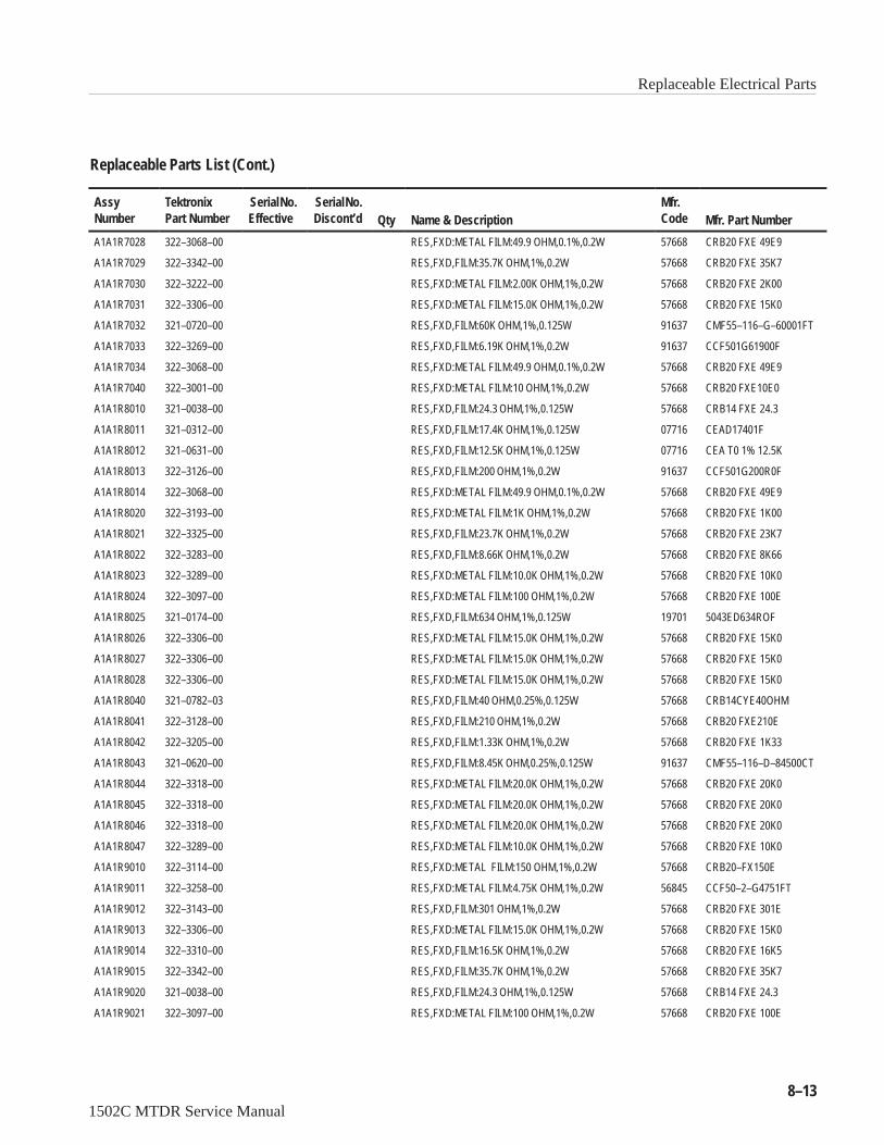
Replaceable Electrical Parts
1502C MTDR Service Manual8–13
Replaceable Parts List (Cont.)
AssyNumber Mfr. Part Number
Mfr.CodeName & DescriptionQty
Serial No.Discont’d
Serial No.Effective
TektronixPart Number
A1A1R7028 322–3068–00 RES,FXD:METAL FILM:49.9 OHM,0.1%,0.2W 57668 CRB20 FXE 49E9
A1A1R7029 322–3342–00 RES,FXD,FILM:35.7K OHM,1%,0.2W 57668 CRB20 FXE 35K7
A1A1R7030 322–3222–00 RES,FXD:METAL FILM:2.00K OHM,1%,0.2W 57668 CRB20 FXE 2K00
A1A1R7031 322–3306–00 RES,FXD:METAL FILM:15.0K OHM,1%,0.2W 57668 CRB20 FXE 15K0
A1A1R7032 321–0720–00 RES,FXD,FILM:60K OHM,1%,0.125W 91637 CMF55–116–G–60001FT
A1A1R7033 322–3269–00 RES,FXD,FILM:6.19K OHM,1%,0.2W 91637 CCF501G61900F
A1A1R7034 322–3068–00 RES,FXD:METAL FILM:49.9 OHM,0.1%,0.2W 57668 CRB20 FXE 49E9
A1A1R7040 322–3001–00 RES,FXD:METAL FILM:10 OHM,1%,0.2W 57668 CRB20 FXE10E0
A1A1R8010 321–0038–00 RES,FXD,FILM:24.3 OHM,1%,0.125W 57668 CRB14 FXE 24.3
A1A1R8011 321–0312–00 RES,FXD,FILM:17.4K OHM,1%,0.125W 07716 CEAD17401F
A1A1R8012 321–0631–00 RES,FXD,FILM:12.5K OHM,1%,0.125W 07716 CEA T0 1% 12.5K
A1A1R8013 322–3126–00 RES,FXD,FILM:200 OHM,1%,0.2W 91637 CCF501G200R0F
A1A1R8014 322–3068–00 RES,FXD:METAL FILM:49.9 OHM,0.1%,0.2W 57668 CRB20 FXE 49E9
A1A1R8020 322–3193–00 RES,FXD:METAL FILM:1K OHM,1%,0.2W 57668 CRB20 FXE 1K00
A1A1R8021 322–3325–00 RES,FXD,FILM:23.7K OHM,1%,0.2W 57668 CRB20 FXE 23K7
A1A1R8022 322–3283–00 RES,FXD,FILM:8.66K OHM,1%,0.2W 57668 CRB20 FXE 8K66
A1A1R8023 322–3289–00 RES,FXD:METAL FILM:10.0K OHM,1%,0.2W 57668 CRB20 FXE 10K0
A1A1R8024 322–3097–00 RES,FXD:METAL FILM:100 OHM,1%,0.2W 57668 CRB20 FXE 100E
A1A1R8025 321–0174–00 RES,FXD,FILM:634 OHM,1%,0.125W 19701 5043ED634ROF
A1A1R8026 322–3306–00 RES,FXD:METAL FILM:15.0K OHM,1%,0.2W 57668 CRB20 FXE 15K0
A1A1R8027 322–3306–00 RES,FXD:METAL FILM:15.0K OHM,1%,0.2W 57668 CRB20 FXE 15K0
A1A1R8028 322–3306–00 RES,FXD:METAL FILM:15.0K OHM,1%,0.2W 57668 CRB20 FXE 15K0
A1A1R8040 321–0782–03 RES,FXD,FILM:40 OHM,0.25%,0.125W 57668 CRB14CYE40OHM
A1A1R8041 322–3128–00 RES,FXD,FILM:210 OHM,1%,0.2W 57668 CRB20 FXE210E
A1A1R8042 322–3205–00 RES,FXD,FILM:1.33K OHM,1%,0.2W 57668 CRB20 FXE 1K33
A1A1R8043 321–0620–00 RES,FXD,FILM:8.45K OHM,0.25%,0.125W 91637 CMF55–116–D–84500CT
A1A1R8044 322–3318–00 RES,FXD:METAL FILM:20.0K OHM,1%,0.2W 57668 CRB20 FXE 20K0
A1A1R8045 322–3318–00 RES,FXD:METAL FILM:20.0K OHM,1%,0.2W 57668 CRB20 FXE 20K0
A1A1R8046 322–3318–00 RES,FXD:METAL FILM:20.0K OHM,1%,0.2W 57668 CRB20 FXE 20K0
A1A1R8047 322–3289–00 RES,FXD:METAL FILM:10.0K OHM,1%,0.2W 57668 CRB20 FXE 10K0
A1A1R9010 322–3114–00 RES,FXD:METAL FILM:150 OHM,1%,0.2W 57668 CRB20–FX150E
A1A1R9011 322–3258–00 RES,FXD:METAL FILM:4.75K OHM,1%,0.2W 56845 CCF50–2–G4751FT
A1A1R9012 322–3143–00 RES,FXD,FILM:301 OHM,1%,0.2W 57668 CRB20 FXE 301E
A1A1R9013 322–3306–00 RES,FXD:METAL FILM:15.0K OHM,1%,0.2W 57668 CRB20 FXE 15K0
A1A1R9014 322–3310–00 RES,FXD,FILM:16.5K OHM,1%,0.2W 57668 CRB20 FXE 16K5
A1A1R9015 322–3342–00 RES,FXD,FILM:35.7K OHM,1%,0.2W 57668 CRB20 FXE 35K7
A1A1R9020 321–0038–00 RES,FXD,FILM:24.3 OHM,1%,0.125W 57668 CRB14 FXE 24.3
A1A1R9021 322–3097–00 RES,FXD:METAL FILM:100 OHM,1%,0.2W 57668 CRB20 FXE 100E
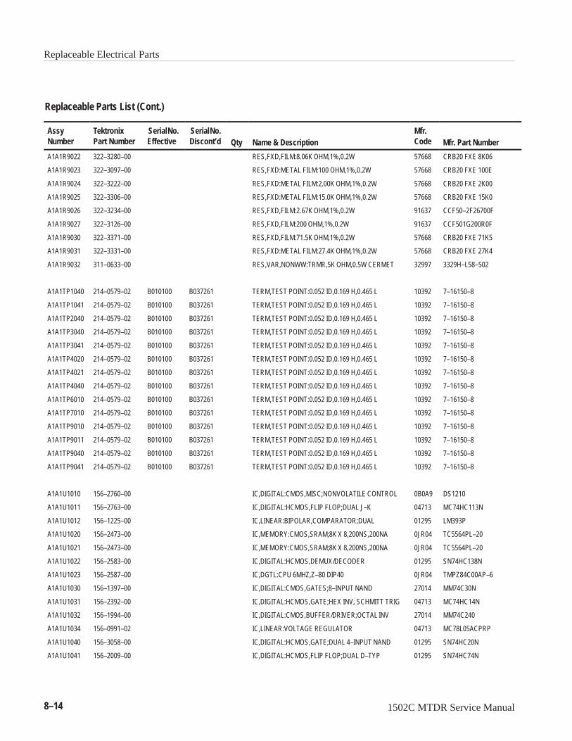
Replaceable Electrical Parts
8–14 1502C MTDR Service Manual
Replaceable Parts List (Cont.)
AssyNumber Mfr. Part Number
Mfr.CodeName & DescriptionQty
Serial No.Discont’d
Serial No.Effective
TektronixPart Number
A1A1R9022 322–3280–00 RES,FXD,FILM:8.06K OHM,1%,0.2W 57668 CRB20 FXE 8K06
A1A1R9023 322–3097–00 RES,FXD:METAL FILM:100 OHM,1%,0.2W 57668 CRB20 FXE 100E
A1A1R9024 322–3222–00 RES,FXD:METAL FILM:2.00K OHM,1%,0.2W 57668 CRB20 FXE 2K00
A1A1R9025 322–3306–00 RES,FXD:METAL FILM:15.0K OHM,1%,0.2W 57668 CRB20 FXE 15K0
A1A1R9026 322–3234–00 RES,FXD,FILM:2.67K OHM,1%,0.2W 91637 CCF50–2F26700F
A1A1R9027 322–3126–00 RES,FXD,FILM:200 OHM,1%,0.2W 91637 CCF501G200R0F
A1A1R9030 322–3371–00 RES,FXD,FILM:71.5K OHM,1%,0.2W 57668 CRB20 FXE 71K5
A1A1R9031 322–3331–00 RES,FXD:METAL FILM:27.4K OHM,1%,0.2W 57668 CRB20 FXE 27K4
A1A1R9032 311–0633–00 RES,VAR,NONWW:TRMR,5K OHM,0.5W CERMET 32997 3329H–L58–502
A1A1TP1040 214–0579–02 B010100 B037261 TERM,TEST POINT:0.052 ID,0.169 H,0.465 L 10392 7–16150–8
A1A1TP1041 214–0579–02 B010100 B037261 TERM,TEST POINT:0.052 ID,0.169 H,0.465 L 10392 7–16150–8
A1A1TP2040 214–0579–02 B010100 B037261 TERM,TEST POINT:0.052 ID,0.169 H,0.465 L 10392 7–16150–8
A1A1TP3040 214–0579–02 B010100 B037261 TERM,TEST POINT:0.052 ID,0.169 H,0.465 L 10392 7–16150–8
A1A1TP3041 214–0579–02 B010100 B037261 TERM,TEST POINT:0.052 ID,0.169 H,0.465 L 10392 7–16150–8
A1A1TP4020 214–0579–02 B010100 B037261 TERM,TEST POINT:0.052 ID,0.169 H,0.465 L 10392 7–16150–8
A1A1TP4021 214–0579–02 B010100 B037261 TERM,TEST POINT:0.052 ID,0.169 H,0.465 L 10392 7–16150–8
A1A1TP4040 214–0579–02 B010100 B037261 TERM,TEST POINT:0.052 ID,0.169 H,0.465 L 10392 7–16150–8
A1A1TP6010 214–0579–02 B010100 B037261 TERM,TEST POINT:0.052 ID,0.169 H,0.465 L 10392 7–16150–8
A1A1TP7010 214–0579–02 B010100 B037261 TERM,TEST POINT:0.052 ID,0.169 H,0.465 L 10392 7–16150–8
A1A1TP9010 214–0579–02 B010100 B037261 TERM,TEST POINT:0.052 ID,0.169 H,0.465 L 10392 7–16150–8
A1A1TP9011 214–0579–02 B010100 B037261 TERM,TEST POINT:0.052 ID,0.169 H,0.465 L 10392 7–16150–8
A1A1TP9040 214–0579–02 B010100 B037261 TERM,TEST POINT:0.052 ID,0.169 H,0.465 L 10392 7–16150–8
A1A1TP9041 214–0579–02 B010100 B037261 TERM,TEST POINT:0.052 ID,0.169 H,0.465 L 10392 7–16150–8
A1A1U1010 156–2760–00 IC,DIGITAL:CMOS,MISC;NONVOLATILE CONTROL 0B0A9 DS1210
A1A1U1011 156–2763–00 IC,DIGITAL:HCMOS,FLIP FLOP;DUAL J–K 04713 MC74HC113N
A1A1U1012 156–1225–00 IC,LINEAR:BIPOLAR,COMPARATOR;DUAL 01295 LM393P
A1A1U1020 156–2473–00 IC,MEMORY:CMOS,SRAM;8K X 8,200NS,200NA 0JR04 TC5564PL–20
A1A1U1021 156–2473–00 IC,MEMORY:CMOS,SRAM;8K X 8,200NS,200NA 0JR04 TC5564PL–20
A1A1U1022 156–2583–00 IC,DIGITAL:HCMOS,DEMUX/DECODER 01295 SN74HC138N
A1A1U1023 156–2587–00 IC,DGTL:CPU 6MHZ,Z–80 DIP40 0JR04 TMPZ84C00AP–6
A1A1U1030 156–1397–00 IC,DIGITAL:CMOS,GATES;8–INPUT NAND 27014 MM74C30N
A1A1U1031 156–2392–00 IC,DIGITAL:HCMOS,GATE;HEX INV, SCHMITT TRIG 04713 MC74HC14N
A1A1U1032 156–1994–00 IC,DIGITAL:CMOS,BUFFER/DRIVER;OCTAL INV 27014 MM74C240
A1A1U1034 156–0991–02 IC,LINEAR:VOLTAGE REGULATOR 04713 MC78L05ACPRP
A1A1U1040 156–3058–00 IC,DIGITAL:HCMOS,GATE;DUAL 4–INPUT NAND 01295 SN74HC20N
A1A1U1041 156–2009–00 IC,DIGITAL:HCMOS,FLIP FLOP;DUAL D–TYP 01295 SN74HC74N

Replaceable Electrical Parts
1502C MTDR Service Manual8–15
Replaceable Parts List (Cont.)
AssyNumber Mfr. Part Number
Mfr.CodeName & DescriptionQty
Serial No.Discont’d
Serial No.Effective
TektronixPart Number
A1A1U1042 156–3180–00 IC,DIGITAL:HCMOS,GATE;TRIPLE 3–INPUT NOR 04713 MC74HC27N
A1A1U1043 156–2463–00 IC,DITIAL:HCMOS,GATE;QUAD 2–INPUT OR 01295 SN74HC32N
A1A1U2011 156–2415–00 IC,DIGITAL:HCMOS,TRANSCEIVER;OCTAL,NONINV 04713 MC74HC245AN
A1A1U2012 156–3110–00 IC,DIGITAL:HCMOS,BUFFER;NONINV OCTAL 27014 MM74HC244N
136–0755–00 SOCKET,DIP:PCB,28 POS,2 X 14,0.1 X 0.6 CTR 09922 DILB28P–108
A1A1U2021 156–2583–00 IC,DIGITAL:HCMOS,DEMUX/DECODER 01295 SN74HC138N
A1A1U2022 156–2583–00 IC,DIGITAL:HCMOS,DEMUX/DECODER 01295 SN74HC138N
A1A1U2023 156–2009–00 IC,DIGITAL:HCMOS,FLIP FLOP;DUAL D–TYP 01295 SN74HC74N
A1A1U2024 156–2583–00 IC,DIGITAL:HCMOS,DEMUX/DECODER 01295 SN74HC138N
A1A1U2025 156–2763–00 IC,DIGITAL:HCMOS,FLIP FLOP;DUAL J–K 04713 MC74HC113N
A1A1U2026 156–2583–00 IC,DIGITAL:HCMOS,DEMUX/DECODER 01295 SN74HC138N
A1A1U2027 156–2763–00 IC,DIGITAL:HCMOS,FLIP FLOP;DUAL J–K 04713 MC74HC113N
A1A1U2030 156–2767–00 IC,DGTL:CHMOS,COUNTER TIMER 82C54 34649 P82C54
A1A1U2031 119–2736–00 CRYSTAL,SCOPE 75378 MXO–55GA–3I–20M
A1A1U2032 156–2096–00 IC,DIGITAL:ALSTTL,FLIP FLOP;QUAD D–TYPE 01295 SN74ALS175N
A1A1U2033 156–2759–00 IC,DIGITAL:ALSTTL,FLIP FLOP;DUAL J–K 01295 74ALS113
A1A1U2034 156–2092–00 IC,DIGITAL:ALSTTL,GATE;QUAD 2–INPUT NOR 01295 SN74ALS02N
A1A1U2036 156–2096–00 IC,DIGITAL:ALSTTL,FLIP FLOP;QUAD D–TYPE 01295 SN74ALS175N
A1A1U2037 156–2098–00 IC,DIGITAL:ALSTTL,COUNTER;SYNCH 4–BIT 01295 SN74ALS161BN
A1A1U2040 156–2437–00 IC,DIGITAL:HCTCMOS,GATE;QUAD 2–INPUT AND 34371 CD74HCT08E17
A1A1U2041 156–2768–00 IC,LINEAR:12 BIT PLUS SIGN 1205 27014 ADC1205
A1A1U2042 156–2759–00 IC,DIGITAL:ALSTTL,FLIP FLOP;DUAL J–K 01295 74ALS113
A1A1U2043 156–2421–00 IC,DIGITAL:HCMOS,FLIP FLOP;QUAD D–TYPE 04713 MC74HC175N
A1A1U2044 156–3107–00 IC,DIGITAL:HCMOS,FLIP FLOP;OCTAL D–TYPE 01295 SN74HC374N
A1A1U2045 156–1752–00 IC,DIGITAL:FTTL,GATE;TRIPLE 3–INPUT NAND 04713 MC 74F10N
A1A1U2046 156–3151–00 IC,INTFC:CMOS,D/A CONVERTER 24355 AD7534JN
A1A1U3010 156–3107–00 IC,DIGITAL:HCMOS,FLIP FLOP;OCTAL D–TYPE 01295 SN74HC374N
A1A1U3020 156–2026–00 IC,DIGITAL:HCMOS,GATE;QUAD 2–INPUT NOR 04713 MC74HC02AN
A1A1U3021 156–3107–00 IC,DIGITAL:HCMOS,FLIP FLOP;OCTAL D–TYPE 01295 SN74HC374N
A1A1U3022 156–2421–00 IC,DIGITAL:HCMOS,FLIP FLOP;QUAD D–TYPE 04713 MC74HC175N
A1A1U3023 156–0927–00 IC,LINEAR:DIGITAL TO ANALOG CONVERTER 04713 MC3410CL
A1A1U3040 156–1173–00 IC,LINEAR:BIPOLAR,VOLT REF;POS,2.5V,1.0% 04713 MC1403U
A1A1U3041 156–0854–00 IC,LINEAR:BIPOLAR,OP–AMP 24355 OP08FP OR PM308–026P
A1A1U3042 156–1114–00 IC,LINEAR:MOS/FET INP,COS/MOS OUT,OP AMP 34371 CA3160E
A1A1U4020 156–3151–00 IC,INTFC:CMOS,D/A CONVERTER 24355 AD7534JN
A1A1U4021 156–1699–00 IC,LINEAR:DUAL BI–FET,OPNL AMPL,LOW OFFSET 01295 TL288CP
A1A1U4040 156–0513–00 IC,MISC:CMOS,ANALOG MUX;8 CHANNEL 04713 MC14051BCP
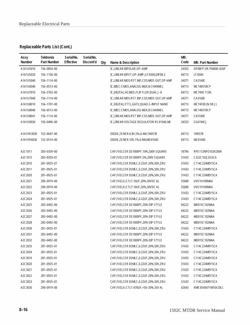
Replaceable Electrical Parts
8–16 1502C MTDR Service Manual
Replaceable Parts List (Cont.)
AssyNumber Mfr. Part Number
Mfr.CodeName & DescriptionQty
Serial No.Discont’d
Serial No.Effective
TektronixPart Number
A1A1U5010 156–0854–00 IC,LINEAR:BIPOLAR,OP–AMP 24355 OP08FP OR PM308–026P
A1A1U5020 156–1156–00 IC,LINEAR:BIFET,OP–AMP;;LF356N,DIP08.3 04713 LF356N
A1A1U5040 156–1114–00 IC,LINEAR:MOS/FET INP,COS/MOS OUT,OP AMP 34371 CA3160E
A1A1U6040 156–0513–00 IC,MISC:CMOS,ANALOG MUX;8 CHANNEL 04713 MC14051BCP
A1A1U7010 156–2763–00 IC,DIGITAL:HCMOS,FLIP FLOP;DUAL J–K 04713 MC74HC113N
A1A1U7040 156–1114–00 IC,LINEAR:MOS/FET INP,COS/MOS OUT,OP AMP 34371 CA3160E
A1A1U8010 156–1707–00 IC,DIGITAL:FTTL,GATE;QUAD 2–INPUT NAND 04713 MC74F00 (N OR J)
A1A1U8040 156–0513–00 IC,MISC:CMOS,ANALOG MUX;8 CHANNEL 04713 MC14051BCP
A1A1U8041 156–1114–00 IC,LINEAR:MOS/FET INP,COS/MOS OUT,OP AMP 34371 CA3160E
A1A1U9030 156–0496–00 IC,LINEAR:VOLTAGE REGULATOR RC4194D,MI 34333 SG4194CJ
A1A1VR3030 152–0647–00 DIODE,ZENER:6.8V,5%,0.4W;1N957B 04713 1N957B
A1A1VR6030 152–0514–00 DIODE,ZENER:10V,1%,0.4W;MZ4104D 04713 MZ4104D
A2C1011 283–0359–00 CAP,FXD,CER DI:1000PF,10%,200V SQUARE 18796 RPE112NPO102K200V
A2C1015 283–0359–01 CAP,FXD,CER DI:1000PF,5%,200V SQUARE 31433 C322C102J2G5CA
A2C2010 281–0925–01 CAP,FXD,CER DI:MLC,0.22UF,20%,50V,ZRU 31433 C114C224M5Y5CA
A2C2011 281–0925–01 CAP,FXD,CER DI:MLC,0.22UF,20%,50V,ZRU 31433 C114C224M5Y5CA
A2C2020 281–0925–01 CAP,FXD,CER DI:MLC,0.22UF,20%,50V,ZRU 31433 C114C224M5Y5CA
A2C2021 290–0974–00 CAP,FXD,ELCTLT:10UF,20%,50VDC AL 55680 UVX1H100MAA
A2C2022 290–0974–00 CAP,FXD,ELCTLT:10UF,20%,50VDC AL 55680 UVX1H100MAA
A2C2023 281–0925–01 CAP,FXD,CER DI:MLC,0.22UF,20%,50V,ZRU 31433 C114C224M5Y5CA
A2C2024 281–0925–01 CAP,FXD,CER DI:MLC,0.22UF,20%,50V,ZRU 31433 C114C224M5Y5CA
A2C2025 283–0492–00 CAP,FXD,CER DI:1000PF,20% DIP STYLE 04222 MD015C102MAA
A2C2026 283–0492–00 CAP,FXD,CER DI:1000PF,20% DIP STYLE 04222 MD015C102MAA
A2C2027 283–0492–00 CAP,FXD,CER DI:1000PF,20% DIP STYLE 04222 MD015C102MAA
A2C2028 283–0492–00 CAP,FXD,CER DI:1000PF,20% DIP STYLE 04222 MD015C102MAA
A2C2030 281–0925–01 CAP,FXD,CER DI:MLC,0.22UF,20%,50V,ZRU 31433 C114C224M5Y5CA
A2C2031 283–0492–00 CAP,FXD,CER DI:1000PF,20% DIP STYLE 04222 MD015C102MAA
A2C2032 283–0492–00 CAP,FXD,CER DI:1000PF,20% DIP STYLE 04222 MD015C102MAA
A2C2033 281–0925–01 CAP,FXD,CER DI:MLC,0.22UF,20%,50V,ZRU 31433 C114C224M5Y5CA
A2C2034 281–0925–01 CAP,FXD,CER DI:MLC,0.22UF,20%,50V,ZRU 31433 C114C224M5Y5CA
A2C3010 281–0925–01 CAP,FXD,CER DI:MLC,0.22UF,20%,50V,ZRU 31433 C114C224M5Y5CA
A2C3020 281–0925–01 CAP,FXD,CER DI:MLC,0.22UF,20%,50V,ZRU 31433 C114C224M5Y5CA
A2C3021 281–0925–01 CAP,FXD,CER DI:MLC,0.22UF,20%,50V,ZRU 31433 C114C224M5Y5CA
A2C3022 281–0925–01 CAP,FXD,CER DI:MLC,0.22UF,20%,50V,ZRU 31433 C114C224M5Y5CA
A2C3023 281–0925–01 CAP,FXD,CER DI:MLC,0.22UF,20%,50V,ZRU 31433 C114C224M5Y5CA
A2C3030 290–0919–00 CAP,FXD,ELCTLT:470UF,+50–20%,35V AL 62643 KME35VB471M10X20LL

Replaceable Electrical Parts
1502C MTDR Service Manual8–17
Replaceable Parts List (Cont.)
AssyNumber Mfr. Part Number
Mfr.CodeName & DescriptionQty
Serial No.Discont’d
Serial No.Effective
TektronixPart Number
A2C3031 290–0919–00 CAP,FXD,ELCTLT:470UF,+50–20%,35V AL 62643 KME35VB471M10X20LL
A2C3032 281–0925–01 CAP,FXD,CER DI:MLC,0.22UF,20%,50V,ZRU 31433 C114C224M5Y5CA
A2C3033 281–0925–01 CAP,FXD,CER DI:MLC,0.22UF,20%,50V,ZRU 31433 C114C224M5Y5CA
A2C3034 281–0925–01 CAP,FXD,CER DI:MLC,0.22UF,20%,50V,ZRU 31433 C114C224M5Y5CA
A2J1020 131–3147–00 CONN,HDR:PCB,MALE,STR,2 X 25,0.1 CTR 22526 66506–032
A2J3030 131–1857–00 CONN,HDR:PCB,MALE,STR,1 X 36,0.1 CTR 58050 082–3644–SS10
A2PS2030 119–2370–00 CONVERTER:DC – AC,15V IN,80V AT 400 HZ 63312 LPS15–1–2
A2Q1020 151–1176–00 XSTR,PWR:MOS,P–CH;100V,1.0A,0.6 OHM 04713 IRFD9120
A2Q1030 151–1176–00 XSTR,PWR:MOS,P–CH;100V,1.0A,0.6 OHM 04713 IRFD9120
A2Q2020 151–1121–01 XSTR,PWR:MOS,N–CH,60V,0.5A,3.0 OHM 17856 VN0606L–TA
A2R1010 322–3385–00 RES,FXD:METAL FILM:100K OHM,1%,0.2W 57668 CRB20 FXE 100K
A2R1011 321–0816–00 RES,FXD,FILM:5K OHM,1%,0.125W 01121 ADVISE
A2R1012 322–3097–00 RES,FXD:METAL FILM:100 OHM,1%,0.2W 57668 CRB20 FXE 100E
A2R1013 322–3347–00 RES,FXD,FILM:40.2K OHM,1%,0.2W 91637 CCF50–2–G40201F
A2R1018 311–1337–00 RES,VAR,NONWW:TRMR,25K OHM,0.5W CERMET 02111 43P253T672
A2R1020 322–3097–00 RES,FXD:METAL FILM:100 OHM,1%,0.2W 57668 CRB20 FXE 100E
A2R1021 322–3385–00 RES,FXD:METAL FILM:100K OHM,1%,0.2W 57668 CRB20 FXE 100K
A2R1022 311–2400–00 RES,VAR,PLASTIC:DUAL 10K,10% NO STOPS 12697 CM45241
A2R1023 322–3385–00 RES,FXD:METAL FILM:100K OHM,1%,0.2W 57668 CRB20 FXE 100K
A2R1024 322–3385–00 RES,FXD:METAL FILM:100K OHM,1%,0.2W 57668 CRB20 FXE 100K
A2R1025 322–3385–00 RES,FXD:METAL FILM:100K OHM,1%,0.2W 57668 CRB20 FXE 100K
A2R1026 322–3385–00 RES,FXD:METAL FILM:100K OHM,1%,0.2W 57668 CRB20 FXE 100K
A2R1027 322–3385–00 RES,FXD:METAL FILM:100K OHM,1%,0.2W 57668 CRB20 FXE 100K
A2R1030 322–3385–00 RES,FXD:METAL FILM:100K OHM,1%,0.2W 57668 CRB20 FXE 100K
A2R1031 322–3059–00 RES,FXD,FILM:40.2 OHM,1%,0.2W 91637 CCF50–2G40R020FT
A2R2010 322–3385–00 RES,FXD:METAL FILM:100K OHM,1%,0.2W 57668 CRB20 FXE 100K
A2R2020 322–3001–00 RES,FXD:METAL FILM:10 OHM,1%,0.2W 57668 CRB20 FXE 10E0
A2R2021 322–3385–00 RES,FXD:METAL FILM:100K OHM,1%,0.2W 57668 CRB20 FXE 100K
A2R2022 321–0523–00 RES,FXD,FILM:2.74M OHM,1%,0.125W 07716 CEA 2.74 M OHM
A2R2024 311–2400–00 RES,VAR,PLASTIC:DUAL 10K,10% NO STOPS 12697 CM45241
A2R2030 322–3385–00 RES,FXD:METAL FILM:100K OHM,1%,0.2W 57668 CRB20 FXE 100K
A2R2031 322–3385–00 RES,FXD:METAL FILM:100K OHM,1%,0.2W 57668 CRB20 FXE 100K
A2R2032 322–3347–00 RES,FXD,FILM:40.2K OHM,1%,0.2W 91637 CCF50–2–G40201F
A2R2034 322–3385–00 RES,FXD:METAL FILM:100K OHM,1%,0.2W 57668 CRB20 FXE 100K
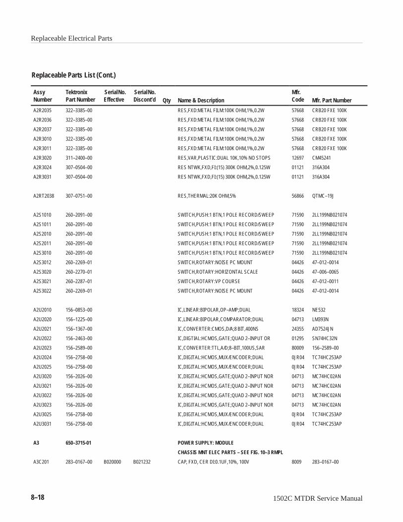
Replaceable Electrical Parts
8–18 1502C MTDR Service Manual
Replaceable Parts List (Cont.)
AssyNumber Mfr. Part Number
Mfr.CodeName & DescriptionQty
Serial No.Discont’d
Serial No.Effective
TektronixPart Number
A2R2035 322–3385–00 RES,FXD:METAL FILM:100K OHM,1%,0.2W 57668 CRB20 FXE 100K
A2R2036 322–3385–00 RES,FXD:METAL FILM:100K OHM,1%,0.2W 57668 CRB20 FXE 100K
A2R2037 322–3385–00 RES,FXD:METAL FILM:100K OHM,1%,0.2W 57668 CRB20 FXE 100K
A2R3010 322–3385–00 RES,FXD:METAL FILM:100K OHM,1%,0.2W 57668 CRB20 FXE 100K
A2R3011 322–3385–00 RES,FXD:METAL FILM:100K OHM,1%,0.2W 57668 CRB20 FXE 100K
A2R3020 311–2400–00 RES,VAR,PLASTIC:DUAL 10K,10% NO STOPS 12697 CM45241
A2R3024 307–0504–00 RES NTWK,FXD,FI:(15) 300K OHM,2%,0.125W 01121 316A304
A2R3031 307–0504–00 RES NTWK,FXD,FI:(15) 300K OHM,2%,0.125W 01121 316A304
A2RT2038 307–0751–00 RES,THERMAL:20K OHM,5% 56866 QTMC–19J
A2S1010 260–2091–00 SWITCH,PUSH:1 BTN,1 POLE RECORD/SWEEP 71590 2LL199NB021074
A2S1011 260–2091–00 SWITCH,PUSH:1 BTN,1 POLE RECORD/SWEEP 71590 2LL199NB021074
A2S2010 260–2091–00 SWITCH,PUSH:1 BTN,1 POLE RECORD/SWEEP 71590 2LL199NB021074
A2S2011 260–2091–00 SWITCH,PUSH:1 BTN,1 POLE RECORD/SWEEP 71590 2LL199NB021074
A2S3010 260–2091–00 SWITCH,PUSH:1 BTN,1 POLE RECORD/SWEEP 71590 2LL199NB021074
A2S3012 260–2269–01 SWITCH,ROTARY:NOISE PC MOUNT 04426 47–012–0014
A2S3020 260–2270–01 SWITCH,ROTARY:HORIZONTAL SCALE 04426 47–006–0065
A2S3021 260–2287–01 SWITCH,ROTARY:VP COURSE 04426 47–012–0011
A2S3022 260–2269–01 SWITCH,ROTARY:NOISE PC MOUNT 04426 47–012–0014
A2U2010 156–0853–00 IC,LINEAR:BIPOLAR,OP–AMP;DUAL 18324 NE532
A2U2020 156–1225–00 IC,LINEAR:BIPOLAR,COMPARATOR;DUAL 04713 LM393N
A2U2021 156–1367–00 IC,CONVERTER:CMOS,D/A;8 BIT,400NS 24355 AD7524JN
A2U2022 156–2463–00 IC,DIGTIAL:HCMOS,GATE;QUAD 2–INPUT OR 01295 SN74HC32N
A2U2023 156–2589–00 IC,CONVERTER:TTL,A/D;8–BIT,100US,SAR 80009 156–2589–00
A2U2024 156–2758–00 IC,DIGITAL:HCMOS,MUX/ENCODER;DUAL 0JR04 TC74HC253AP
A2U2025 156–2758–00 IC,DIGITAL:HCMOS,MUX/ENCODER;DUAL 0JR04 TC74HC253AP
A2U3020 156–2026–00 IC,DIGITAL:HCMOS,GATE;QUAD 2–INPUT NOR 04713 MC74HC02AN
A2U3021 156–2026–00 IC,DIGITAL:HCMOS,GATE;QUAD 2–INPUT NOR 04713 MC74HC02AN
A2U3022 156–2026–00 IC,DIGITAL:HCMOS,GATE;QUAD 2–INPUT NOR 04713 MC74HC02AN
A2U3023 156–2026–00 IC,DIGITAL:HCMOS,GATE;QUAD 2–INPUT NOR 04713 MC74HC02AN
A2U3025 156–2758–00 IC,DIGITAL:HCMOS,MUX/ENCODER;DUAL 0JR04 TC74HC253AP
A2U3031 156–2758–00 IC,DIGITAL:HCMOS,MUX/ENCODER;DUAL 0JR04 TC74HC253AP
A3 650–3715-01 POWER SUPPLY: MODULE
CHASSIS MNT ELEC PARTS – SEE FIG. 10–3 RMPL
A3C201 283–0167–00 B020000 B021232 CAP, FXD, CER DI:0.1UF,10%, 100V 8009 283–0167–00

Replaceable Electrical Parts
1502C MTDR Service Manual8–19
Replaceable Parts List (Cont.)
AssyNumber Mfr. Part Number
Mfr.CodeName & DescriptionQty
Serial No.Discont’d
Serial No.Effective
TektronixPart Number
A3F101 159–0029–01 FUSE CARTRIDGE:BUSSMAN ONLY 71400 MDL3/10
A3F101 159–0054–00 FUSE CARTRIDGE:3AG, 0.15A, 250V 75915 313.150
A3FL1 119–3488–00 FILTER, RFI:1A, 115V/230VAC, 50/60HW OGV52 FN328–1/01
A3L201 120–1458–00 B020000 B021232 XFMR,RF:TOROID 1980PF, 100A, 130V 80009 120–1458–00
A3R101 307–0449–00 RES, V SENSITIVE:1900PF, 100A, 130V 34371 V130LA20A
A3S201 260–2372–00 SWITCH,ROTARY:VOLTAGE SELECTOR 61935 033–4501
A3T201 120–1607–00 B020000 B021232 XFMR,PWR:DUAL PRI 115/230VAC, 5060HZ 80009 120–1607–00
120–1922–00 B021233 XFMR,PWR:DUAL PRI 115/230VAC, 5060HZ 0JR03 Z–9 1260A
A3A1 670–9286–XX CIRCUIT BD ASSY:POWER SUPPLY
A3A1C1010 290–0997–00 CAP,FXD,ELCTLT:3000UF,–10% +75%,75V 24165 53D268
A3A1C1011 283–0220–02 CAP,FXD,CER DI:0.01UF,20%,50V 04222 AR205C103MAATRSTDII
A3A1C1012 283–0359–01 CAP,FXD,CER DI:1000PF,5%,200V 31433 C322C102J2G5CA
A3A1C1013 281–0925–01 CAP,FXD,CER DI:MLC,0.22UF,20%,50V 31433 C114C224M5Y5CA
A3A1C1014 283–0359–01 CAP,FXD,CER DI:1000PF,5%,200V 31433 C322C102J2G5CA
A3A1C1015 283–0359–01 CAP,FXD,CER DI:1000PF,5%,200V 31433 C322C102J2G5CA
A3A1C1016 283–0107–00 CAP,FXD,CER DI:51PF,5%,200V 04222 SR202A510JAA
A3A1C1030 283–0059–02 CAP,FXD,CER DI:1UF,20%,50V 04222 SR305C105MAATRSTDII
A3A1C1031 283–0059–02 CAP,FXD,CER DI:1UF,20%,50V 04222 SR305C105MAATRSTDII
A3A1C1032 290–0536–04 CAP,FXD,ELCTLT:10UF,20%,25V 24165 199D106X0025CA1
A3A1C1033 290–0536–04 CAP,FXD,ELCTLT:10UF,20%,25V 24165 199D106X0025CA1
A3A1C1034 283–0177–00 CAP,FXD,CER DI:1UF,+80–20%,25V 04222 SR305E105ZAA
A3A1C1035 283–0177–00 CAP,FXD,CER DI:1UF,+80–20%,25V 04222 SR305E105ZAA
A3A1C1036 283–0177–00 CAP,FXD,CER DI:1UF,+80–20%,25V 04222 SR305E105ZAA
A3A1C1037 290–0973–01 CAP,FXD,ELCTLT:100UF,20%,25VDC AL 62643 SME35VB101M8X11FT
A3A1C1038 283–0177–00 CAP,FXD,CER DI:1UF,+80–20%,25V 04222 SR305E105ZAA
A3A1C2010 290–0973–01 CAP,FXD,ELCTLT:100UF,20%,25VDC AL 62643 SME35VB101M8X11FT
A3A1C2011 290–0517–00 CAP,FXD,ELCTLT:6.8UF,20%,35V 24165 199D685X0035DA1
A3A1C2012 290–0973–01 CAP,FXD,ELCTLT:100UF,20%,25VDC AL 62643 SME35VB101M8X11FT
A3A1C2013 283–0198–00 CAP,FXD,CER DI:0.22UF,20%,50V 04222 SR305C224MAA
A3A1C2020 283–0051–00 CAP,FXD,CER DI:0.0033UF,5%,100V 04222 SR301A332JAA
A3A1C2021 290–0745–02 CAP,FXD,ELCTLT:22UF,+50–10%,25V,AL 55680 UVX2A220MPA
A3A1C2022 283–0010–00 CAP,FXD,CER DI:0.05UF,+80–20%,50V 04222 SR305E503ZAA
A3A1C2023 283–0220–02 CAP,FXD,CER DI:0.01UF,20%,50V 04222 AR205C103MAATRSTDII
A3A1C2024 281–0925–01 CAP,FXD,CER DI:0.22UF,20%,50V 31433 C114C224M5Y5CA
A3A1C2025 290–0846–00 CAP,FXD,ELCTLT:47UF,+75–20%,35V AL 62643 CEUSM1J470
A3A1C2030 281–0925–01 CAP,FXD,CER DI:0.22UF,20%,50V 31433 C114C224M5Y5CA

Replaceable Electrical Parts
8–20 1502C MTDR Service Manual
Replaceable Parts List (Cont.)
AssyNumber Mfr. Part Number
Mfr.CodeName & DescriptionQty
Serial No.Discont’d
Serial No.Effective
TektronixPart Number
A3A1C2031 283–0059–02 CAP,FXD,CER DI:1UF,20%,50V 04222 SR305C105MAATRSTDII
A3A1CR1010 152–0406–00 DIODE,RECT:BRIDGE,250V,3A,1.2VF 14936 GBPC604
A3A1CR1011 152–0322–00 DIODE DVC,DI:SCHOTTKY,SI,15V,1.2PF 50434 5082–2672
A3A1CR1030 152–0582–00 DIODE,RECT:SCHTKY,20V,3A,.475VF,80A 04713 1N5820
A3A1CR1031 152–0582–00 DIODE,RECT:SCHTKY,20V,3A,.475VF,80A 04713 1N5820
A3A1CR1032 152–0581–00 DIODE,RECT:SCHTKY,20V,1A,.450VF,25A 14936 SB120–5
A3A1CR1033 152–0581–00 DIODE,RECT:SCHTKY,20V,1A,.450VF,25A 14936 SB120–5
A3A1CR1034 152–0779–00 DIODE,RECT:FAST RCVRY;BRIDGE,200V 80009 152–0779–00
A3A1CR2010 152–0601–00 DIODE,RECT:ULTRA FAST;150V,25NS,35A 04713 MUR115
A3A1CR2011 152–1165–00 DIODE,RECT:600V,4A,50NS 04713 MUR460RL
A3A1CR2012 152–0582–00 DIODE,RECT:SCHTKY,20V,3A,.475VF,80A 04713 1N5820
A3A1CR2013 152–0322–00 DIODE DVC,DI:SCHOTTKY,SI,15V,1.2PF 50434 5082–2672
A3A1CR2014 152–0322–00 DIODE DVC,DI:SCHOTTKY,SI,15V,1.2PF 50434 5082–2672
A3A1CR2015 152–0836–00 DIODE DVC,DI:RECT,SI,1A,40V 1N5819 80009 152–0836–00
A3A1CR2016 152–0141–02 DIODE,SIG:ULTRA FAST;40V,150MA,4NS,2PF 14433 1N4152
A3A1CR2020 152–0322–00 DIODE DVC,DI:SCHOTTKY,SI,15V,1.2PF 50434 5082–2672
A3A1CR2021 152–0601–00 DIODE,RECT:ULTRA FAST;150V,25NS,35A 04713 MUR115
A3A1CR2030 152–0333–00 DIODE DVC,DI:SW,SI,55V,200MA 12969 NDP261
A3A1CR2031 152–0333–00 DIODE DVC,DI:SW,SI,55V,200MA 12969 NDP261
A3A1J1010 131–4177–00 CONN,HDR:PCB,MALE,STR,1 X 31,0.15 CTR 80009 131–4177–00
A3A1J1030 131–3445–00 CONN,HDR:PCB,MALE,RTANG,2 X 7,0.1 CTR 80009 131–3445–00
A3A1J2010 131–1857–00 CONN,HDR:PCB,MALE,STR,1 X 36,0.1 CTR 58050 082–3644–SS10
A3A1L1010 108–1230–00 COIL,RF:FIXED,100UH,5% POT CORE 54937 500–3990
A3A1L2020 108–1230–00 COIL,RF:FIXED,100UH,5% POT CORE 54937 500–3990
A3A1Q1010 151–1176–00 XSTR,PWR:MOS,P–CH;100V,1.0A,0.6 OHM 04713 IRFD9120
A3A1Q1011 151–1176–00 XSTR,PWR:MOS,P–CH;100V,1.0A,0.6 OHM 04713 IRFD9120
A3A1Q1012 151–0736–00 XSTR:NPN,SI,TO–92 2N4401 04713 2N4401
A3A1Q2010 151–0736–00 XSTR:NPN,SI,TO–92 2N4401 04713 2N4401
A3A1Q2011 151–1176–00 XSTR,PWR:MOS,P–CH;100V,1.0A,0.6 OHM 04713 IRFD9120
A3A1Q2012 151–1176–00 XSTR,PWR:MOS,P–CH;100V,1.0A,0.6 OHM 04713 IRFD9120
A3A1Q2020 151–0188–00 XSTR,SIG:BIPOLAR,PNP;40V,200MA,250MHZ,AMP 04713 2N3906
A3A1Q2021 151–0424–00 XSTR:NPN,SI,TO–92 MPS2369A 04713 MPS2369A
A3A1Q2022 151–1136–00 XSTR,PWR:MOS,N–CH;100V,14A,0.16 OHM 04713 MTP12N10E
A3A1Q2030 151–1063–00 XSTR,PWR:MOS,N–CH;60V,0.8A,0.8 OHM 04713 IRFD113
A3A1Q2031 151–1063–00 XSTR,PWR:MOS,N–CH;60V,0.8A,0.8 OHM 04713 IRFD113
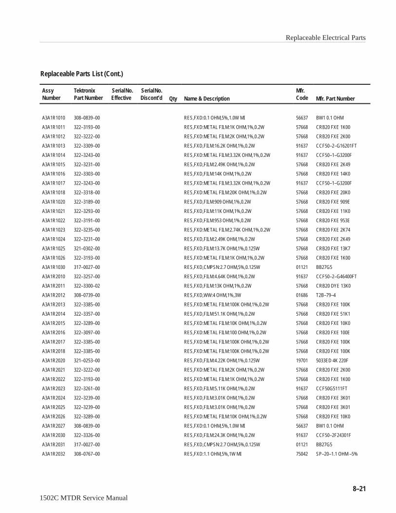
Replaceable Electrical Parts
1502C MTDR Service Manual8–21
Replaceable Parts List (Cont.)
AssyNumber Mfr. Part Number
Mfr.CodeName & DescriptionQty
Serial No.Discont’d
Serial No.Effective
TektronixPart Number
A3A1R1010 308–0839–00 RES,FXD:0.1 OHM,5%,1.0W MI 56637 BW1 0.1 OHM
A3A1R1011 322–3193–00 RES,FXD:METAL FILM:1K OHM,1%,0.2W 57668 CRB20 FXE 1K00
A3A1R1012 322–3222–00 RES,FXD:METAL FILM:2K OHM,1%,0.2W 57668 CRB20 FXE 2K00
A3A1R1013 322–3309–00 RES,FXD,FILM:16.2K OHM,1%,0.2W 91637 CCF50–2–G16201FT
A3A1R1014 322–3243–00 RES,FXD:METAL FILM:3.32K OHM,1%,0.2W 91637 CCF50–1–G3200F
A3A1R1015 322–3231–00 RES,FXD,FILM:2.49K OHM,1%,0.2W 57668 CRB20 FXE 2K49
A3A1R1016 322–3303–00 RES,FXD,FILM:14K OHM,1%,0.2W 57668 CRB20 FXE 14K0
A3A1R1017 322–3243–00 RES,FXD:METAL FILM:3.32K OHM,1%,0.2W 91637 CCF50–1–G3200F
A3A1R1018 322–3318–00 RES,FXD:METAL FILM:20K OHM,1%,0.2W 57668 CRB20 FXE 20K0
A3A1R1020 322–3189–00 RES,FXD,FILM:909 OHM,1%,0.2W 57668 CRB20 FXE 909E
A3A1R1021 322–3293–00 RES,FXD,FILM:11K OHM,1%,0.2W 57668 CRB20 FXE 11K0
A3A1R1022 322–3191–00 RES,FXD,FILM:953 OHM,1%,0.2W 57668 CRB20 FXE 953E
A3A1R1023 322–3235–00 RES,FXD:METAL FILM:2.74K OHM,1%,0.2W 57668 CRB20 FXE 2K74
A3A1R1024 322–3231–00 RES,FXD,FILM:2.49K OHM,1%,0.2W 57668 CRB20 FXE 2K49
A3A1R1025 321–0302–00 RES,FXD,FILM:13.7K OHM,1%,0.125W 57668 CRB20 FXE 13K7
A3A1R1026 322–3193–00 RES,FXD:METAL FILM:1K OHM,1%,0.2W 57668 CRB20 FXE 1K00
A3A1R1030 317–0027–00 RES,FXD,CMPSN:2.7 OHM,5%,0.125W 01121 BB27G5
A3A1R2010 322–3257–00 RES,FXD,FILM:4.64K OHM,1%,0.2W 91637 CCF50–2–G46400FT
A3A1R2011 322–3300–02 RES,FXD,FILM:13K OHM,1%,0.2W 57668 CRB20 DYE 13K0
A3A1R2012 308–0739–00 RES,FXD,WW:4 OHM,1%,3W 01686 T2B–79–4
A3A1R2013 322–3385–00 RES,FXD:METAL FILM:100K OHM,1%,0.2W 57668 CRB20 FXE 100K
A3A1R2014 322–3357–00 RES,FXD,FILM:51.1K OHM,1%,0.2W 57668 CRB20 FXE 51K1
A3A1R2015 322–3289–00 RES,FXD:METAL FILM:10K OHM,1%,0.2W 57668 CRB20 FXE 10K0
A3A1R2016 322–3097–00 RES,FXD:METAL FILM:100 OHM,1%,0.2W 57668 CRB20 FXE 100E
A3A1R2017 322–3385–00 RES,FXD:METAL FILM:100K OHM,1%,0.2W 57668 CRB20 FXE 100K
A3A1R2018 322–3385–00 RES,FXD:METAL FILM:100K OHM,1%,0.2W 57668 CRB20 FXE 100K
A3A1R2020 321–0253–00 RES,FXD,FILM:4.22K OHM,1%,0.125W 19701 5033ED 4K 220F
A3A1R2021 322–3222–00 RES,FXD:METAL FILM:2K OHM,1%,0.2W 57668 CRB20 FXE 2K00
A3A1R2022 322–3193–00 RES,FXD:METAL FILM:1K OHM,1%,0.2W 57668 CRB20 FXE 1K00
A3A1R2023 322–3261–00 RES,FXD,FILM:5.11K OHM,1%,0.2W 91637 CCF50G5111FT
A3A1R2024 322–3239–00 RES,FXD,FILM:3.01K OHM,1%,0.2W 57668 CRB20 FXE 3K01
A3A1R2025 322–3239–00 RES,FXD,FILM:3.01K OHM,1%,0.2W 57668 CRB20 FXE 3K01
A3A1R2026 322–3289–00 RES,FXD:METAL FILM:10K OHM,1%,0.2W 57668 CRB20 FXE 10K0
A3A1R2027 308–0839–00 RES,FXD:0.1 OHM,5%,1.0W MI 56637 BW1 0.1 OHM
A3A1R2030 322–3326–00 RES,FXD,FILM:24.3K OHM,1%,0.2W 91637 CCF50–2F24301F
A3A1R2031 317–0027–00 RES,FXD,CMPSN:2.7 OHM,5%,0.125W 01121 BB27G5
A3A1R2032 308–0767–00 RES,FXD:1.1 OHM,5%,1W MI 75042 SP–20–1.1 OHM –5%

Replaceable Electrical Parts
8–22 1502C MTDR Service Manual
Replaceable Parts List (Cont.)
AssyNumber Mfr. Part Number
Mfr.CodeName & DescriptionQty
Serial No.Discont’d
Serial No.Effective
TektronixPart Number
A3A1S2010 260–2370–00 SWITCH,TOGGLE:SPDT,3A,250VAC 09353 E101SD1AQE
A3A1T1030 120–1608–00 XFMR,PWR:SW,40KHZ,IN 16.2V,OUT +/–15V 34MA 0JR03 120–1608–00
A3A1T1031 120–0487–00 XFMR,TOROID:5 TURNS,BIFILAR,3T2 0JR03 120–0487–00
A3A1TP1010 214–0579–02 B020000 B021172 TERM,TEST POINT:0.052 ID,0.169 H,0.465 L 10392 7–16150–8
A3A1TP1020 214–0579–02 B020000 B021172 TERM,TEST POINT:0.052 ID,0.169 H,0.465 L 10392 7–16150–8
A3A1TP2010 214–0579–02 B020000 B021172 TERM,TEST POINT:0.052 ID,0.169 H,0.465 L 10392 7–16150–8
A3A1TP2030 214–0579–02 B020000 B021172 TERM,TEST POINT:0.052 ID,0.169 H,0.465 L 10392 7–16150–8
A3A1U1010 156–0933–00 IC,LINEAR:REGULATOR,PULSE WIDTH 34333 SG3524N
A3A1U1011 156–1173–00 IC,LINEAR:BIPOLAR,VOLT REF;POS,2.5V,1.0% 04713 MC1403U
A3A1U1020 156–1225–00 IC,LINEAR:BIPOLAR,COMPARATOR;DUAL 04713 LM393N
A3A1U1021 156–1225–00 IC,LINEAR:BIPOLAR,COMPARATOR;DUAL 04713 LM393N
A3A1U1022 156–1173–00 IC,LINEAR:BIPOLAR,VOLT REF;POS,2.5V,1.0% 04713 MC1403U
A3A1U1023 156–0933–00 IC,LINEAR:REGULATOR,PULSE WIDTH 34333 SG3524N
A3A1U1024 156–0366–00 IC,DIGITAL:CMOS,FLIP FLOP;DUAL D–TYPE 04713 MC14013BCP
A3A1U2010 156–1161–00 IC,LINEAR:BIPOLAR,VOLT REG;POS,ADJ 04713 LM317T
A3A1U2030 156–0494–00 IC,DIGITAL:CMOS,BUFFER/DRIVER;HEX INV 04713 MC14049UBCP
A3A1VR1012 152–0217–00 DIODE,ZENER:8.2V,5%,0.4W 14552 TD3810979
A4 670–9291–XX CKT BD ASSY:S/R DRIVER SAMPLER
A4C1010 281–0775–00 CAP,FXD,CER DI:0.1UF,20%,50V 04222 SA105E104MAA
A4C1011 281–0775–00 CAP,FXD,CER DI:0.1UF,20%,50V 04222 SA105E104MAA
A4C1020 290–0723–00 CAP,FXD,ELCTLT:150UF,20%,6V 24165 196D157X0006PE3
A4C1030 281–0775–00 CAP,FXD,CER DI:0.1UF,20%,50V 04222 SA105E104MAA
A4C1040 281–0775–00 CAP,FXD,CER DI:0.1UF,20%,50V 04222 SA105E104MAA
A4C1041 290–0804–01 CAP,FXD,ELCTLT:10UF,20%,25V AL 0H1N5 CEUSM1E100T12
A4C1050 281–0765–00 CAP,FXD,CER DI:100PF,5%,100V 04222 SA102A101JAA
A4C1060 281–0775–00 CAP,FXD,CER DI:0.1UF,20%,50V 04222 SA105E104MAA
A4C1061 281–0775–00 CAP,FXD,CER DI:0.1UF,20%,50V 04222 SA105E104MAA
A4C1070 281–0775–00 CAP,FXD,CER DI:0.1UF,20%,50V 04222 SA105E104MAA
A4C1071 281–0775–00 CAP,FXD,CER DI:0.1UF,20%,50V 04222 SA105E104MAA
A4C2010 290–0536–04 CAP,FXD,ELCTLT:10UF,20%,25V 24165 199D106X0025CA1
A4C2011 283–0359–01 CAP,FXD,CER DI:1000PF,5%,200V 31433 C322C102J2G5CA

Replaceable Electrical Parts
1502C MTDR Service Manual8–23
Replaceable Parts List (Cont.)
AssyNumber Mfr. Part Number
Mfr.CodeName & DescriptionQty
Serial No.Discont’d
Serial No.Effective
TektronixPart Number
A4C2012 283–0359–01 CAP,FXD,CER DI:1000PF,5%,200V 31433 C322C102J2G5CA
A4C2020 290–0523–00 CAP,FXD,ELCTLT:2.2UF,20%,20V 24165 196D225X0020HA1
A4C2021 290–0523–00 CAP,FXD,ELCTLT:2.2UF,20%,20V 24165 196D225X0020HA1
A4C2022 290–0523–00 CAP,FXD,ELCTLT:2.2UF,20%,20V 24165 196D225X0020HA1
A4C2023 290–0523–00 CAP,FXD,ELCTLT:2.2UF,20%,20V 24165 196D225X0020HA1
A4C2024 290–0523–00 CAP,FXD,ELCTLT:2.2UF,20%,20V 24165 196D225X0020HA1
A4C2025 283–0359–01 CAP,FXD,CER DI:1000PF,5%,200V 31433 C322C102J2G5CA
A4C2026 283–0359–01 CAP,FXD,CER DI:1000PF,5%,200V 31433 C322C102J2G5CA
A4C2030 281–0861–00 CAP,FXD,CER DI:270PF,5%,50V 04222 SA101A271JAA
A4C2031 283–0193–00 CAP,FXD,CER DI:510PF,2%,100V 04222 SR201A511GAA
A4C2040 281–0775–00 CAP,FXD,CER DI:0.1UF,20%,50V 04222 SA105E104MAA
A4C2041 281–0775–00 CAP,FXD,CER DI:0.1UF,20%,50V 04222 SA105E104MAA
A4C2042 281–0861–00 CAP,FXD,CER DI:270PF,5%,50V 04222 SA101A271JAA
A4C2050 281–0775–00 CAP,FXD,CER DI:0.1UF,20%,50V 04222 SA105E104MAA
A4C2051 290–0522–01 CAP,FXD,ELCTLT:1UF,20%,50V 31433 T355B105M050AS
A4C2052 281–0775–00 CAP,FXD,CER DI:0.1UF,20%,50V 04222 SA105E104MAA
A4C2053 285–0627–00 CAP,FXD,PLASTIC:0.0033UF,5%,100V 01002 61F10AC332
A4C2072 290–0782–01 CAP,FXD,ELCTLT:4.7UF,20%,35VDC AL 55680 UVX1V4R7MAA1TD
A4C2080 290–0844–00 CAP,FXD,ELCTLT:100UF,+75–20%,35WVDC AL 62643 CEUSM1V101
A4C2081 290–0844–00 CAP,FXD,ELCTLT:100UF,+75–20%,35WVDC AL 62643 CEUSM1V101
A4C2082 283–0359–01 CAP,FXD,CER DI:1000PF,5%,200V 31433 C322C102J2G5CA
A4C2083 283–0359–01 CAP,FXD,CER DI:1000PF,5%,200V 31433 C322C102J2G5CA
A4C3010 290–0844–00 CAP,FXD,ELCTLT:100UF,+75–20%,35WVDC AL 62643 CEUSM1V101
A4C3011 290–0844–00 CAP,FXD,ELCTLT:100UF,+75–20%,35WVDC AL 62643 CEUSM1V101
A4C3020 281–0775–00 CAP,FXD,CER DI:0.1UF,20%,50V 04222 SA105E104MAA
A4C3030 283–0193–00 CAP,FXD,CER DI:510PF,2%,100V 04222 SR201A511GAA
A4C3060 281–0775–00 CAP,FXD,CER DI:0.1UF,20%,50V 04222 SA105E104MAA
A4C3061 281–0775–00 CAP,FXD,CER DI:0.1UF,20%,50V 04222 SA105E104MAA
A4C3062 290–0844–00 CAP,FXD,ELCTLT:100UF,+75–20%,35WVDC AL 62643 CEUSM1V101
A4C3063 290–0844–00 CAP,FXD,ELCTLT:100UF,+75–20%,35WVDC AL 62643 CEUSM1V101
A4C3064 283–0359–01 CAP,FXD,CER DI:1000PF,5%,200V 31433 C322C102J2G5CA
A4C3065 283–0359–01 CAP,FXD,CER DI:1000PF,5%,200V 31433 C322C102J2G5CA
A4C3070 281–0775–00 CAP,FXD,CER DI:0.1UF,20%,50V 04222 SA105E104MAA
A4C3080 281–0775–00 CAP,FXD,CER DI:0.1UF,20%,50V 04222 SA105E104MAA
A4CR1030 152–0322–00 DIODE DVC,DI:SCHOTTKY,SI,15V,1.2PF 21847 A2X600
A4CR1031 152–0141–02 DIODE,SIG:ULTRA FAST;40V,150MA,4NS,2PF 01295 1N4152R
A4CR1032 152–0141–02 DIODE,SIG:ULTRA FAST;40V,150MA,4NS,2PF 01295 1N4152R

Replaceable Electrical Parts
8–24 1502C MTDR Service Manual
Replaceable Parts List (Cont.)
AssyNumber Mfr. Part Number
Mfr.CodeName & DescriptionQty
Serial No.Discont’d
Serial No.Effective
TektronixPart Number
A4CR1040 152–0322–00 DIODE DVC,DI:SCHOTTKY,SI,15V,1.2PF 21847 A2X600
A4CR2050 152–0333–00 DIODE DVC,DI:SW,SI,55V,200MA,DO–351N461D 12969 NDP261
A4CR2051 152–0333–00 DIODE DVC,DI:SW,SI,55V,200MA,DO–351N461D 12969 NDP261
A4CR2052 152–0333–00 DIODE DVC,DI:SW,SI,55V,200MA,DO–351N461D 12969 NDP261
A4CR3020 152–0322–00 DIODE DVC,DI:SCHOTTKY,SI,15V,1.2PF 21847 A2X600
A4CR3021 152–0322–00 DIODE DVC,DI:SCHOTTKY,SI,15V,1.2PF 21847 A2X600
A4J3040 131–3360–00 CONN,HDR:PCB,MALE,STR,2 X 10,0.1 CTR 53387 3592–6002
A4L2080 108–1032–00 COIL,RF:FXD,225UH,20% TOROIDAL 0JR03 108–1032–00
A4L2081 108–1032–00 COIL,RF:FXD,225UH,20% TOROIDAL 0JR03 108–1032–00
A4Q1030 151–0190–00 XSTR,SIG:BIPOLAR,NPN;40V,200MA,300MHZ,AMP 01295 SKA3703
A4Q1060 151–1103–00 XSTR,SIG:DMOS,N–CH;ENH,30V,50MA,45 OHM 17856 DM1140/SD210DE
A4Q2030 151–0271–00 XSTR,SIG:BIPOLAR,PNP;15V,30MA,2.0GHZ,AMP 01295 SKA4504
A4Q2040 151–0190–00 XSTR,SIG:BIPOLAR,NPN;40V,200MA,300MHZ,AMP 01295 SKA3703
A4Q2050 151–0188–00 XSTR,SIG:BIPOLAR,PNP;40V,200MA,250MHZ,AMP 04713 2N3906
A4R1010 315–0301–00 RES,FXD,FILM:300 OHM,5%,0.25W 01121 CB3015
A4R1020 315–0102–00 RES,FXD,FILM:1K OHM,5%,0.25W 01121 CB1025
A4R1030 315–0101–00 RES,FXD,FILM:100 OHM,5%,0.25W 01121 CB1015
A4R1031 315–0103–00 RES,FXD,FILM:10K OHM,5%,0.25W 01121 CB1035
A4R1040 321–1249–00 RES,FXD,FILM:3.88K OHM,1%,0.125W 01121 ADVISE
A4R1041 321–0612–03 RES,FXD,FILM:500 OHM,0.25,0.125W 19701 5033RC500R0C
A4R1042 311–1921–00 RES,VAR,NONWW:TRMR,250 OHM,10%,0.5W 02111 63S251T602
A4R1050 322–3308–00 RES,FXD,FILM:15.8K OHM,1%,0.2W 57668 CRB20 FXE 15K8
A4R1051 322–3289–00 RES,FXD:METAL FILM:10K OHM,1%,0.2W 57668 CRB20 FXE 10K0
A4R1052 315–0101–00 RES,FXD,FILM:100 OHM,5%,0.25W 01121 CB1015
A4R1053 315–0101–00 RES,FXD,FILM:100 OHM,5%,0.25W 01121 CB1015
A4R1060 322–3331–00 RES,FXD:METAL FILM:27.4K OHM,1%,0.2W 57668 CRB20 FXE 27K4
A4R1061 322–3289–00 RES,FXD:METAL FILM:10K OHM,1%,0.2W 57668 CRB20 FXE 10K0
A4R1062 322–3364–00 RES,FXD,FILM:60.4K OHM,1%,0.2W 57668 CRB20 FXE 60K4
A4R1063 322–3297–00 RES,FXD,FILM:12.1K OHM,1%,0.2W 57668 CRB20 FXE 12K1
A4R1064 322–3289–00 RES,FXD:METAL FILM:10K OHM,1%,0.2W 57668 CRB20 FXE 10K0
A4R1065 322–3364–00 RES,FXD,FILM:60.4K OHM,1%,0.2W 57668 CRB20 FXE 60K4
A4R1066 322–3297–00 RES,FXD,FILM:12.1K OHM,1%,0.2W 57668 CRB20 FXE 12K1
A4R1070 322–3289–00 RES,FXD:METAL FILM:10K OHM,1%,0.2W 57668 CRB20 FXE 10K0
A4R1071 315–0100–00 RES,FXD,FILM:10 OHM,5%,0.25W 01121 CB1005

Replaceable Electrical Parts
1502C MTDR Service Manual8–25
Replaceable Parts List (Cont.)
AssyNumber Mfr. Part Number
Mfr.CodeName & DescriptionQty
Serial No.Discont’d
Serial No.Effective
TektronixPart Number
A4R1072 315–0100–00 RES,FXD,FILM:10 OHM,5%,0.25W 01121 CB1005
A4R2030 315–0300–00 RES,FXD,FILM:30 OHM,5%,0.25W 01121 CB3005
A4R2031 315–0103–00 RES,FXD,FILM:10K OHM,5%,0.25W 01121 CB1035
A4R2040 315–0101–00 RES,FXD,FILM:100 OHM,5%,0.25W 01121 CB1015
A4R2041 315–0511–00 RES,FXD,FILM:510 OHM,5%,0.25W 01121 CB5115
A4R2042 315–0101–00 RES,FXD,FILM:100 OHM,5%,0.25W 01121 CB1015
A4R2043 315–0101–00 RES,FXD,FILM:100 OHM,5%,0.25W 01121 CB1015
A4R2045 315–0121–00 RES,FXD,FILM:120 OHM,5%,0.25W 01121 CB1215
A4R2046 315–0473–00 RES,FXD,FILM:47K OHM,5%,0.25W 01121 CB4735
A4R2047 315–0243–00 RES,FXD,FILM:24K OHM,5%,0.25W 01121 CB2435
A4R2048 315–0101–00 RES,FXD,FILM:100 OHM,5%,0.25W 01121 CB1015
A4R2049 315–0562–00 RES,FXD,FILM:5.6K OHM,5%,0.25W 01121 CB5625
A4R2050 315–0101–00 RES,FXD,FILM:100 OHM,5%,0.25W 01121 CB1015
A4R2051 315–0203–00 RES,FXD,FILM:20K OHM,5%,0.25W 01121 CB2035
A4R2052 315–0101–00 RES,FXD,FILM:100 OHM,5%,0.25W 01121 CB1015
A4R2053 315–0562–00 RES,FXD,FILM:5.6K OHM,5%,0.25W 01121 CB5625
A4R2054 315–0752–00 RES,FXD,FILM:7.5K OHM,5%,0.25W 01121 CB7525
A4R3020 315–0100–00 RES,FXD,FILM:10 OHM,5%,0.25W 01121 CB1005
A4R3021 322–3344–00 RES,FXD,FILM:37.4K OHM,1%,0.2W 57668 CRB20 FXE 37K4
A4R3032 317–0027–00 RES,FXD,CMPSN:2.7 OHM,5%,0.125W 01121 BB27G5
A4R3033 317–0027–00 RES,FXD,CMPSN:2.7 OHM,5%,0.125W 01121 BB27G5
A4R3040 322–3268–00 RES,FXD,FILM:6.04K OHM,1%,0.2W 57668 CRB20 FXE 6K04
A4R3050 315–0100–00 RES,FXD,FILM:10 OHM,5%,0.25W 01121 CB1005
A4R3051 315–0100–00 RES,FXD,FILM:10 OHM,5%,0.25W 01121 CB1005
A4R3061 322–3396–00 RES,FXD,FILM:130K OHM,1%,0.2W 57668 CRB20 FXE 130K
A4R3062 321–0631–03 RES,FXD,FILM:12.5K OHM,0.25%,0.125W 01121 ADVISE
A4R3070 322–3389–00 RES,FXD,FILM:110K OHM,0.25%,0.2W 56845 CCF–50–2–1103F
A4R3071 321–0645–00 RES,FXD,FILM:100K OHM,0.5%,0.125W 19701 5033RC1003D
A4R3080 321–0645–00 RES,FXD,FILM:100K OHM,0.5%,0.125W 19701 5033RC1003D
A4T1020 120–0582–00 XFMR,TOROID:2 WINDINGS,067–0572–00 0JR03 120–0582–00
A4TP1020 214–0579–00 B020000 B021172 TERM,TEST POINT:0.052 ID,0.169 H,0.465 L 80009 214–0579–00
A4TP1021 214–0579–00 B020000 B021172 TERM,TEST POINT:0.052 ID,0.169 H,0.465 L 80009 214–0579–00
A4TP1030 214–0579–00 B020000 B021172 TERM,TEST POINT:0.052 ID,0.169 H,0.465 L 80009 214–0579–00
A4TP1060 214–0579–00 B020000 B021172 TERM,TEST POINT:0.052 ID,0.169 H,0.465 L 80009 214–0579–00
A4TP1080 214–0579–00 B020000 B021172 TERM,TEST POINT:0.052 ID,0.169 H,0.465 L 80009 214–0579–00
A4TP1081 214–0579–00 B020000 B021172 TERM,TEST POINT:0.052 ID,0.169 H,0.465 L 80009 214–0579–00

Replaceable Electrical Parts
8–26 1502C MTDR Service Manual
Replaceable Parts List (Cont.)
AssyNumber Mfr. Part Number
Mfr.CodeName & DescriptionQty
Serial No.Discont’d
Serial No.Effective
TektronixPart Number
A4TP1082 214–0579–00 B020000 B021172 TERM,TEST POINT:0.052 ID,0.169 H,0.465 L 80009 214–0579–00
A4TP1083 214–0579–00 B020000 B021172 TERM,TEST POINT:0.052 ID,0.169 H,0.465 L 80009 214–0579–00
A4TP1084 214–0579–00 B020000 B021172 TERM,TEST POINT:0.052 ID,0.169 H,0.465 L 80009 214–0579–00
A4TP2060 214–0579–00 B020000 B021172 TERM,TEST POINT:0.052 ID,0.169 H,0.465 L 80009 214–0579–00
A4TP3020 214–0579–00 B020000 B021172 TERM,TEST POINT:0.052 ID,0.169 H,0.465 L 80009 214–0579–00
A4U1010 119–2369–01 HYBRID:TDR FRONT END 80009 119–2369–01
A4U1050 156–0853–00 IC,LINEAR:BIPOLAR,OP–AMP;DUAL 04713 LM358N
A4U1070 156–0853–00 IC,LINEAR:BIPOLAR,OP–AMP;DUAL 04713 LM358N
A4U2050 156–1291–00 IC,LINEAR:BIFET,OP–AMP;DUAL,LOW PWR 01295 TL062CP
A4U2070 156–1490–00 IC,LINEAR:VOLTAGE REFERENCE 2–PIN 34371 ICL8069CCSQ
A4U3030 156–2761–00 IC,DIGITAL:HCMOS,MULTIVIBRATOR 04713 MC74HC221N
A4U3070 156–0853–00 IC,LINEAR:BIPOLAR,OP–AMP;DUAL 04713 LM358N
WIRE ASSEMBLIES
W1010 174–0955–00 CA ASSY,RF:50 OHM COAX,4.75 L(FROM A4U1010 TO FRONT PANEL J100)
060D9 174–0955–00
W2010 174–0950–00 CA ASSY,SP,ELEC:26,28 AWG,11.0 L(TO OPTION PORT)
060D9 174–0950–00
W2020 174–1539–00 CA ASSY,SP,ELEC:4,22 AWG,9.0 L,RIBBON(P0WER SUPPLY A3A1J2010 TO BATTERYINCLUDES 5A FUSE)
060D9 174–1539–00
W5040 174–0953–00 CA ASSY,SP,ELEC:14,26 AWG,6.125 L(FROM A3A1J1030 TO A1A1J5040)
060D9 174–0953–00
W6010 174–0951–00 CA ASSY,SP,ELEC:20,28 AWG,300V,RMS(FROM DISPLAY MODULE A5 AND A2A1J1020 TOA1A1J6010)
060D9 174–0951–00
W9010 174–0952–00 CA ASSY,SP,ELEC:20,28 AWG,6.125 L,RIBBON(FROM A4J3040 TO A1A1J9010)
060D9 174–0952–00
J101 174–0957–00 B010100 B021232 CA ASSY,PWR:2 STRAND W/CONNECTOR(FROM A3T201 TO POWER SUPPLY)
80009 174–0957–00
198–5460–01 WIRE SET,ELEC:POWER SUPPLY MODULE(CONN AND GROUND WIRE, SET OF TWO)
060D9 198–5460–01

1502C MTDR Service Manual 9–1
Diagrams
General Information
Each assembly in the instrument is assigned an assembly number (e.g., A1). Theassembly number appears in the title block of the schematic diagram, in the title forthe circuit board component location illustration, and in the lookup table for theschematic diagram component locator. The replaceable parts list is arranged byassemblies in numerical sequence: the components are listed by componentnumber.
The schematic diagram and circuit board component location illustration havegrids. A lookup table with the grid coordinates is provided for to help you locate thecomponent.
The component locator lookup table provides an alphanumeric listing of all circuitnumbers for the circuit boards in the instrument. Corresponding to each circuitnumber is a schematic page reference, the locator for that schematic page, and thelocator for the circuit board.
The locator lists are given for each circuit board, ordered by that board’s assemblynumber:
An example entry is as follows:
Schematic Schematic BoardPage Locator Locator
↓ ↓ ↓ C10306 2B D8 C1
Read: Capacitor C10306 is found on schematic 2B in grid D8. Its physical locationis grid C1 on the circuit board.
A locator list and circuit board grid are also given on each circuit board illustration.
Graphic symbols and class designation letters are based on ANSI standards.
Logic symbology reflects the actual part function, not the logic function performed.Therefore, logic symbols should reflect manufacturer’s data.
Electrical components shown on the diagrams are in the following units:
Resistors = Ohm (Ω)
Assembly Numbers
Grid Coordinates
Electrical Parts Locator
Schematic Symbols
Component Values

Diagrams
9–2 1502C MTDR Service Manual
Capacitors = Farad (F)Inductors = Henry (H)
All capacitors and inductors indicate their units; resistors only indicate theappropriate scale factor.
Scale factors are given by the following standard:
M mega 106
k kilo 103
m milli 10–3
u micro (µ) 10–6
n nano 10–9
p pico 10–12
A numbering method is used to identify assemblies, subassemblies, and parts. Anexample of this numbering method and typical expansions is as follows:
A23A2R1234 = A23 A2 R1234↓ ↓ ↓
Assembly Subassembly CircuitNumber Number Number
Read: resistor 1234 of subassembly 2 of assy 23.
Only circuit numbers appear on the schematics, circuit board illustrations, andelectrical parts locator lists. Each schematic and illustration is marked with itsassembly number. Assembly numbers are also marked on the mechanical explodedview located in the replaceable mechanical parts list. A component number isobtained by adding the assembly number prefix to the circuit number. Thecomponent number may then be used to reference a part in the replaceable electricalparts list.
Component Number

Diagrams
1502C MTDR Service Manual 9–3
Refer todiagram 3A Test point
Internaladjustment
Connectorto 3D
Instrument type
Board name
Functional name
Assemblypart number
Assemblyreferencenumber
Diagramnumber
Figure 9–1: Special Schematic Symbols

Diagrams
9–4 1502C MTDR Service Manual
A1 – MAIN
Back Side Components
CIRCUIT SCHEM LOCATIONNUMBER PAGE SCHEM BRD
BT1010 2 G2 A1
C1010 2 G4 A1C1011 2 A4 A1C1020 2 B4 B1C1021 2 D1 B1C1022 2 E2 B1C1023 2 E1 B1
C1024 2 F1 B1C1030 2 C1 C1C1031 2 A4 C1C1032 2 F1 C1C1040 3 B4 D1C1041 3 B4 D1
C1042 1 G2 D1C1043 2 A4 D1C2010 5 G3 A2C2011 5 G2 A2C2012 2 B4 A2C2013 4 A4 A2
C2014 4 B4 A2C2015 5 F3 A2C2016 5 F2 A2C2020 3 B4 B2C2021 7 B4 B2C2030 7 C4 C2
C2031 7 B2 C2C2032 7 C4 C2C2033 7 C4 C2C2034 7 D4 C2C2035 7 D4 C2C2036 7 D4 C2
C2037 7 E4 C2C2038 7 E4 C2C2039 6 B1 C2C2040 6 C3 D2C2041 6 D3 D2C2042 6 B3 D2
C2043 6 E4 D2C2044 7 E4 D2C2045 7 B2 D2C2046 6 D3 D2
CIRCUIT SCHEM LOCATIONNUMBER PAGE SCHEM BRD
C3020 2 B4 B3C3021 8A E4 B3C3022 8A E4 B3C3023 8A D3 B3C3030 8B A1 C3C3040 8B A2 D3
C3041 6 C3 D3C3042 6 G2 D3C3043 6 B2 D3C3044 6 B2 D3C3045 6 H1 D3C3046 6 H1 D3
C3047 8B A2 D3C3048 8B A1 D3C4020 8B D3 B4C4021 8A E3 B4C4022 8A G3 B4C4030 8B B1 C4
C4040 8B C2 D4C4041 1 F2 D4C5010 8B E3 A5C5020 8B D4 B5C5021 8B B4 B5C5022 8B B3 B5
C5023 8B F2 B5C5024 8B G3 B5C5025 8B G3 B5C5030 8B E3 C5C5031 8B C1 C5C5032 8B C2 C5
C5033 8B B3 C5C5040 6 F2 D5C5041 6 G1 D5C5042 6 G1 D5C6030 8B E2 C6C6031 8B B1 C6
C6032 8B D1 C6C7010 8B G1 A7C7020 8B G1 B7C7021 8B E1 B7C7022 8B F2 B7C7023 8B D2 B7
CIRCUIT SCHEM LOCATIONNUMBER PAGE SCHEM BRD
C7030 8B D2 C7C7040 6 D2 D7C7041 6 G1 D7C7042 6 G1 D7C7043 1 F2 D7C8010 8A F2 A8
C8020 8A D2 B8C8021 8A C2 B8C8022 8A A1 B8C8023 8B G4 B8C8024 8B E2 B8C8040 6 C2 D8
C9010 8A G2 A9C9011 8A F1 A9C9020 8A D1 B9C9021 8A C1 B9C9022 8A D2 B9C9023 8A C2 B9
C9024 8A C1 B9C9025 8B G4 B9C9030 5 B1 C9C9031 5 C1 C9C9032 5 B1 C9C9033 5 B2 C9
C9034 5 B1 C9C9035 5 C1 C9
CR1020 2 F2 B1CR1021 2 F2 B1CR1022 2 F1 B1CR1023 2 F1 B1CR3031 8B B2 C3CR4030 8A F3 C4
CR4031 8B A3 C4CR4032 8B C2 C4CR5030 8B C3 C5CR5040 8B B2 D5CR8020 8A C2 B8CR9010 8A G2 A9
J2010 1 C3 A2J5040 † 1 E2 D5J6010 1 F3 A6
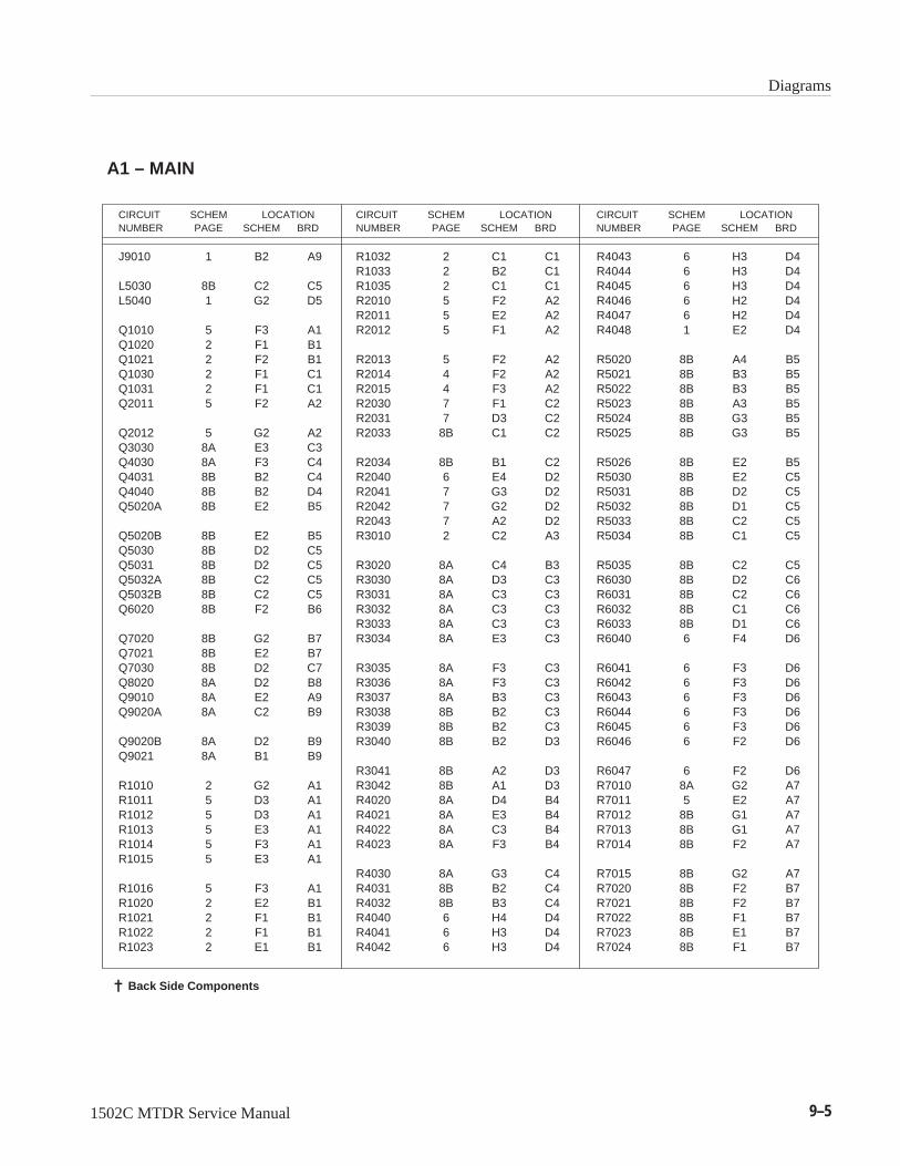
Diagrams
1502C MTDR Service Manual 9–5
A1 – MAIN
Back Side Components
CIRCUIT SCHEM LOCATIONNUMBER PAGE SCHEM BRD
J9010 1 B2 A9
L5030 8B C2 C5L5040 1 G2 D5
Q1010 5 F3 A1Q1020 2 F1 B1Q1021 2 F2 B1Q1030 2 F1 C1Q1031 2 F1 C1Q2011 5 F2 A2
Q2012 5 G2 A2Q3030 8A E3 C3Q4030 8A F3 C4Q4031 8B B2 C4Q4040 8B B2 D4Q5020A 8B E2 B5
Q5020B 8B E2 B5Q5030 8B D2 C5Q5031 8B D2 C5Q5032A 8B C2 C5Q5032B 8B C2 C5Q6020 8B F2 B6
Q7020 8B G2 B7Q7021 8B E2 B7Q7030 8B D2 C7Q8020 8A D2 B8Q9010 8A E2 A9Q9020A 8A C2 B9
Q9020B 8A D2 B9Q9021 8A B1 B9
R1010 2 G2 A1R1011 5 D3 A1R1012 5 D3 A1R1013 5 E3 A1R1014 5 F3 A1R1015 5 E3 A1
R1016 5 F3 A1R1020 2 E2 B1R1021 2 F1 B1R1022 2 F1 B1R1023 2 E1 B1
CIRCUIT SCHEM LOCATIONNUMBER PAGE SCHEM BRD
R1032 2 C1 C1R1033 2 B2 C1R1035 2 C1 C1R2010 5 F2 A2R2011 5 E2 A2R2012 5 F1 A2
R2013 5 F2 A2R2014 4 F2 A2R2015 4 F3 A2R2030 7 F1 C2R2031 7 D3 C2R2033 8B C1 C2
R2034 8B B1 C2R2040 6 E4 D2R2041 7 G3 D2R2042 7 G2 D2R2043 7 A2 D2R3010 2 C2 A3
R3020 8A C4 B3R3030 8A D3 C3R3031 8A C3 C3R3032 8A C3 C3R3033 8A C3 C3R3034 8A E3 C3
R3035 8A F3 C3R3036 8A F3 C3R3037 8A B3 C3R3038 8B B2 C3R3039 8B B2 C3R3040 8B B2 D3
R3041 8B A2 D3R3042 8B A1 D3R4020 8A D4 B4R4021 8A E3 B4R4022 8A C3 B4R4023 8A F3 B4
R4030 8A G3 C4R4031 8B B2 C4R4032 8B B3 C4R4040 6 H4 D4R4041 6 H3 D4R4042 6 H3 D4
CIRCUIT SCHEM LOCATIONNUMBER PAGE SCHEM BRD
R4043 6 H3 D4R4044 6 H3 D4R4045 6 H3 D4R4046 6 H2 D4R4047 6 H2 D4R4048 1 E2 D4
R5020 8B A4 B5R5021 8B B3 B5R5022 8B B3 B5R5023 8B A3 B5R5024 8B G3 B5R5025 8B G3 B5
R5026 8B E2 B5R5030 8B E2 C5R5031 8B D2 C5R5032 8B D1 C5R5033 8B C2 C5R5034 8B C1 C5
R5035 8B C2 C5R6030 8B D2 C6R6031 8B C2 C6R6032 8B C1 C6R6033 8B D1 C6R6040 6 F4 D6
R6041 6 F3 D6R6042 6 F3 D6R6043 6 F3 D6R6044 6 F3 D6R6045 6 F3 D6R6046 6 F2 D6
R6047 6 F2 D6R7010 8A G2 A7R7011 5 E2 A7R7012 8B G1 A7R7013 8B G1 A7R7014 8B F2 A7
R7015 8B G2 A7R7020 8B F2 B7R7021 8B F2 B7R7022 8B F1 B7R7023 8B E1 B7R7024 8B F1 B7

Diagrams
9–6 1502C MTDR Service Manual
A1 – MAIN
Back Side Components
CIRCUIT SCHEM LOCATIONNUMBER PAGE SCHEM BRD
R7025 8B E2 B7R7026 8B F2 B7R7027 8B F2 B7R7028 8B F3 B7R7029 8B F1 B7R7030 8B F2 C7
R7031 8B E2 C7R7032 8B D2 C7R7033 8B D2 C7R7034 8B D2 C7R7040 1 F2 D7R8010 8A F2 A8
R8011 8A E2 A8R8012 8A E2 A8R8013 8A E2 A8R8014 8A D2 A8R8020 8A D1 B8R8021 8A E2 B8
R8022 8A E2 B8R8023 8A E2 B8R8024 8A D2 B8R8025 8A C2 B8R8026 8A B2 B8R8027 8A B1 B8
R8028 8A B1 B8R8040 6 E3 D8R8041 6 E3 D8R8042 6 E3 D8R8043 6 E2 D8R8044 6 C2 D8
R8045 6 C2 D8R8046 6 C2 D8R8047 6 C2 D8R9010 8A H2 A9R9011 8A H2 A9R9012 8A F2 A9
R9013 8A F1 A9R9014 8A E2 A9R9015 8A E1 A9R9020 8A E1 B9R9021 8A C1 B9R9022 8A C2 B9
CIRCUIT SCHEM LOCATIONNUMBER PAGE SCHEM BRD
R9023 8A D2 B9R9024 8A D2 B9R9025 8A C2 B9R9026 8A B1 B9R9027 8A B1 B9R9030 5 B2 C9
R9031 5 B2 C9R9032 5 B2 C9
TP1040 2 C1 D1TP1041 7 E1 D1TP2040 7 B1 D2TP3040 7 G3 D3TP3041 7 G3 D3TP4020 8A H4 B4
TP4021 8A H3 B4TP4040 6 H2 D4TP6010 8B F4 A6TP7010 8B G2 A7TP9010 8B E3 A9TP9011 8A G2 A9
TP9040 8A B2 D9TP9041 6 A2 D9
U1010 2 G2 A1U1011A 4 D4 A1U1011B 5 C3 A1U1012A 5 E2 A1U1012B 5 E3 A1U1020 2 G3 B1
U1021 2 E3 B1U1022 2 E2 B1U1023 2 D1 B1U1030 2 B1 C1U1031A 2 G2 C1U1031B 2 C1 C1
U1031C 3 B2 C1U1031D 2 C1 C1U1031E 2 A2 C1U1031F 2 A3 C1U1032A 2 B1 C1U1032B 2 B2 C1
CIRCUIT SCHEM LOCATIONNUMBER PAGE SCHEM BRD
U1034 7 B1 C1U1040A 3 B3 D1U1040B 3 C3 D1U1041A 3 D4 D1U1041B 3 E4 D1U1042A 3 C4 D1
U1042B 3 B1 D1U1042C 3 B3 D1U1043A 2 D2 D1U1043B 3 E2 D1U1043C 2 B3 D1U1043D 2 C3 D1
U2011 4 D1 A2U2012A 4 D3 A2U2012B 4 D2 A2U2020 2 D3 B2U2021 3 E3 B2U2022 3 G1 B2
U2023A 2 C4 B2U2023B 3 G3 B2U2024 3 F2 B2U2025A 7 F1 B2U2025B 7 G1 B2U2026 3 F2 B2
U2027A 7 C4 B2U2027B 7 A4 B2U2030 7 B2 C2U2031 7 C1 C2U2032 7 C2 C2U2033A 3 B2 C2
U2033B 7 F1 C2U2034A 7 G1 C2U2034B 7 E2 C2U2034C 7 C3 C2U2034D 7 B4 C2U2036 7 E2 C2
U2037 7 E3 C2U2040A 6 B3 D2U2040B 5 B3 D2U2040C 3 C2 D2U2040D 7 E1 D2U2041 6 C3 D2

Diagrams
1502C MTDR Service Manual 9–7
A1 – MAIN
Back Side Components
CIRCUIT SCHEM LOCATIONNUMBER PAGE SCHEM BRD
U2042A 7 D1 D2U2042B 7 D1 D2U2043 7 D3 D2U2044 6 B1 D2U2045A 7 G2 D2U2045B 7 G3 D2
U2045C 7 G3 D2U2046 6 B3 D2U3010 2 B3 A3U3020A 3 F4 B3U3020B 3 F4 B3U3020C 3 B3 B3
U3020D 3 B4 B3U3021 8A B3 B3U3022 8A B4 B3U3023 8A C3 B3U3040 6 B3 D3U3041 6 B2 D3
U3042 6 G2 D3U4020 8B C3 B4U4021A 8A D4 B4U4021B 8A G3 B4U4040 6 G3 D4U5010 8B E4 A5
U5020 8B B4 B5U5040 6 E2 D5U6040 6 E3 D6U7010A 8A G1 A7U7010B 8A D3 A7U7040 6 D2 D7
U8010A 8A G2 A8U8010B 8A F2 A8U8010C 8A F2 A8U8040 6 D3 D8U8041 6 C2 D8U9030 5 C1 C9
VR3030 8A B3 C3VR6030 8B C1 C6

Diagrams
9–8 1502C MTDR Service Manual
A2 – FRONT PANEL
Back Side Components
CIRCUIT SCHEM LOCATIONNUMBER PAGE SCHEM BRD
C1011 10 D1 A1C1015 10 B1 A1C2010 10 A3 A2C2011 10 A3 A2C2020 10 C1 B2C2021 10 E1 B2
C2022 10 E2 B2C2023 10 G4 B2C2024 10 B1 B2C2025 10 B3 B2C2026 10 E4 B2C2027 10 B3 B2
C2028 10 E4 B2C2030 10 C1 C2C2031 10 C3 C2C2032 10 C4 C2C2033 10 D3 C2C2034 10 D4 C2
C3010 10 A4 A3C3020 10 H4 B3C3021 10 C1 B3C3022 10 C1 B3C3023 10 B1 B3C3030 † 10 D3 C3
C3031 † 10 D3 C3C3032 10 C3 C3C3033 10 C3 C3C3034 10 B4 C3
J1020 † 10 F1 C1J3030 † 10 H1 C3
PS2030 † 10 F2 C2
Q1020 10 C1 B1Q1030 10 D3 C1Q2020 10 A1 B2
R1010 10 B2 A1R1011 10 D1 A1R1012 10 E2 A1R1013 10 B2 A1R1014 10 D1 A1R1020 10 D1 B1
CIRCUIT SCHEM LOCATIONNUMBER PAGE SCHEM BRD
R1021 10 C1 B1R1022A 10 C3 B1R1022B 10 C4 B1R1023 10 C2 B1R1024 10 B1 B1R1025 10 B1 B1
R1026 10 A1 B1R1027 10 C3 B1R1030 10 D2 C1R1031 10 D2 C1R2010 10 B2 A2R2020 10 F1 B2
R2021 10 B3 B2R2022 10 C1 B2R2024A 10 A3 B2R2024B 10 A3 B2R2030 10 D4 C2R2031 10 E4 C2
R2032 10 D3 C2R2034 10 B3 C2R2035 10 B3 C2R2036 10 C3 C2R2037 10 C4 C2R2038 10 D3 C2
R3010 10 B4 A3R3011 10 B3 A3R3020A 10 D4 B3R3020B 10 D4 B3R3024 10 D1 B3R3031 10 E1 C3
S1010 10 A2 A1S1011 10 A2 A1S2010 10 A3 A2S2011 10 A3 A2S3010 10 A4 A3S3012 10 C2 A3
S3020 10 E2 B3S3021 10 D3 B3S3022 10 C4 B3
U2010A 10 D1 A2U2010B 99 D2 A2
CIRCUIT SCHEM LOCATIONNUMBER PAGE SCHEM BRD
U2020A 10 B1 B2U2020B 10 C3 B2U2021 10 C1 B2U2022A 99 F2 B2U2022B 10 B1 B2U2022B 99 F2 B2
U2022C 10 B2 B2U2023 10 E3 B2U2024 10 G1 B2U2025 10 G2 B2U3020A 10 B3 B3U3020B 10 B3 B3
U3020C 10 B3 B3U3020D 10 B3 B3U3021A 10 B1 B3U3021B 99 C2 B3U3021C 10 B2 B3U3021D 10 B2 B3
U3022A 10 B3 B3U3022B 10 B3 B3U3022C 10 B2 B3U3022D 10 B3 B3U3023A 10 B4 B3U3023B 10 B3 B3
U3023C 10 B4 B3U3023D 10 B4 B3U3025 10 G2 B3U3031 10 G3 C3

Diagrams
1502C MTDR Service Manual 9–9
A3A1 – POWER SUPPLY
Back Side Components
CIRCUIT SCHEM LOCATIONNUMBER PAGE SCHEM BRD
C1010 † 1A B2 A1C1011 1A B3 A1C1012 1A C4 A1C1013 1A F2 A1C1014 1A D3 A1C1015 1A C4 A1
C1016 1A C4 A1C1030 1A G5 C1C1031 1A G5 C1C1032 1A F4 C1C1033 1A F4 C1C1034 1A F3 C1
C1035 1A F4 C1C1036 1A G5 C1C1037 1A G5 C1C1038 1A F6 C1C2010 1A F3 A2C2011 1A A5 A2
C2012 1A F3 A2C2013 1A B6 A2C2020 1A C7 B2C2021 1A D5 B2C2022 1A C7 B2C2023 1A C7 B2
C2024 1A E7 B2C2025 1A E6 B2C2030 1A E8 C2C2031 1A G6 C2
CR1010 1A B2 A1CR1011 1A E3 A1CR1030 1A F4 C1CR1031 1A F5 C1CR1032 1A F5 C1CR1033 1A F5 C1
CR1034 1A F3 C1
CIRCUIT SCHEM LOCATIONNUMBER PAGE SCHEM BRD
CR2010 1A E3 A2CR2011 1A G2 A2CR2012 1A G2 A2CR2013 1A G2 A2CR2014 1A G2 A2CR2015 1A G2 A2
CR2016 1A A5 A2CR2020 1A D7 B2CR2021 1A D6 B2CR2030 1A F6 C2CR2031 1A F6 C2
J1010 1A B2 A1J1030 1A G4 C1J2010 1A H2 A2
L1010 1A E3 A1L2020 1A D6 B2
Q1010 1A E2 A1Q1011 1A F2 A1Q1012 1A E2 A1Q2010 1A B6 A2Q2011 1A B5 A2Q2012 1A B5 A2
Q2020 1A D7 B2Q2021 1A D8 B2Q2022 1A D7 B2Q2030 1A F6 C2Q2031 1A F6 C2
R1010 1A B3 A1R1011 1A B3 A1R1012 1A B3 A1R1013 1A C3 A1R1014 1A D2 A1R1015 1A B3 A1
R1016 1A B3 A1
CIRCUIT SCHEM LOCATIONNUMBER PAGE SCHEM BRD
R1017 1A D3 A1R1018 1A C4 A1R1020 1A B6 B1R1021 1A B5 B1R1022 1A B7 B1R1023 1A B7 B1
R1024 1A C7 B1R1025 1A C6 B1R1026 1A E7 B1R1030 1A G5 C1R2010 1A F2 A2R2011 1A F2 A2
R2012 1A G2 A2R2013 1A A6 A2R2014 1A A6 A2R2015 1A B6 A2R2016 1A A5 A2R2017 1A A5 A2
R2018 1A B5 A2R2020 1A C7 B2R2021 1A D7 B2R2022 1A D7 B2R2023 1A D7 B2R2024 1A C7 B2
R2025 1A D7 B2R2026 1A D8 B2R2027 1A D7 B2R2030 1A G6 C2R2031 1A G4 C2R2032 1A G7 C2
S2010 1A A5 A2
T1030 1A F5 C1T1031 1A G6 C1
TP1010 1A A3 A1

Diagrams
9–10 1502C MTDR Service Manual
A3A1 – POWER SUPPLY
Back Side Components
CIRCUIT SCHEM LOCATIONNUMBER PAGE SCHEM BRD
TP1020 1A G2 B1TP2010 1A B2 A2TP2030 1A E6 C2
U1010 1A C4 A1U1011 1A D3 A1U1020A 1A B6 B1U1020B 1A B6 B1U1021A 1A B7 B1U1021B 1A B8 B1
U1022 1A C6 B1U1023 1A C7 B1U1024B 1A E7 B1U2010 1A G2 A2U2030A 1A E8 C2U2030B 1A F7 C2
U2030C 1A F7 C2U2030D 1A F7 C2U2030E 1A F7 C2
VR1012 1A D2 A1

Diagrams
1502C MTDR Service Manual 9–11
A4– S/R DRIVER SAMPLER
Back Side Components
CIRCUIT SCHEM LOCATIONNUMBER PAGE SCHEM BRD
C1010 9A E5 A1C1011 9A E5 A1C1020 9A D2 B1C1030 9A F2 C1C1040 9A D2 D1C1041 9A B3 D1
C1050 9A F7 E1C1060 9A G7 F1C1061 9A F8 F1C1070 9A D4 G1C1071 9A D5 G1C2010 9A E2 A2
C2011 9A E5 A2C2012 9A E4 A2C2020 9A E3 B2C2021 9A E3 B2C2022 9A E3 B2C2023 9A E4 B2
C2024 9A E4 B2C2025 9A E3 B2C2026 9A E4 B2C2030 9A B4 C2C2031 9A B6 C2C2040 9A B4 D2
C2041 9A F6 D2C2042 9A A4 D2C2050 9A F7 E2C2051 9A D6 E2C2052 9A D7 E2C2053 9A E7 E2
C2072 9A A2 G2C2080 9A B8 H2C2081 9A B7 H2C2082 9A B8 H2C2083 9A B7 H2C3010 9A E5 A3
C3011 9A E5 A3C3020 9A B5 B3C3030 9A C7 C3C3060 9A A1 F3
CIRCUIT SCHEM LOCATIONNUMBER PAGE SCHEM BRD
C3061 9A B2 F3C3062 9A A1 F3C3063 9A C2 F3C3064 9A A1 F3C3065 9A B2 F3C3070 9A A2 G3
C3080 9A B2 H3
CR1030 9A B4 C1CR1031 9A F2 C1CR1032 9A F3 C1CR1040 9A D1 D1CR2050 9A E7 E2CR2051 9A E6 E2
CR2052 9A E7 E2CR3020 9A B5 B3CR3021 9A C5 B3
J3040 9A G3 D3
L2080 9A A7 H2L2081 9A A7 H2
Q1030 9A E2 C1Q1060 9A E6 F1Q2030 9A B4 C2Q2040 9A D6 D2Q2050 9A D6 E2
R1010 9A E4 A1R1020 9A C4 B1R1030 9A E1 C1R1031 9A E2 C1R1040 9A D1 D1R1041 9A D2 D1
R1042 9A D2 D1R1050 9A F7 E1R1051 9A F7 E1R1052 9A G7 E1R1053 9A F8 E1R1060 9A F6 F1
R1061 9A D6 F1
CIRCUIT SCHEM LOCATIONNUMBER PAGE SCHEM BRD
R1062 9A C5 F1R1063 9A C5 F1R1064 9A C5 F1R1065 9A D4 F1R1066 9A D5 F1R1070 9A D4 G1
R1071 9A D4 G1R1072 9A D5 G1R2030 9A B4 C2R2031 9A B4 C2R2040 9A B3 D2R2041 9A B4 D2
R2042 9A F6 D2R2043 9A F7 D2R2045 9A A4 D2R2046 9A C6 D2R2047 9A D6 D2R2048 9A D6 D2
R2049 9A D6 D2R2050 9A E7 E2R2051 9A D6 E2R2052 9A D7 E2R2053 9A E7 E2R2054 9A E7 E2
R3020 9A B5 B3R3021 9A B6 B3R3032 9A F4 C3R3033 9A E4 C3R3040 9A B7 D3R3050 9A A1 E3
R3051 9A B2 E3R3061 9A A1 F3R3062 9A A2 F3R3070 9A A2 G3R3071 9A B2 G3R3080 9A B1 H3
T1020 9A C4 B1
TP1020 9A E5 B1TP1021 9A D4 B1

Diagrams
9–12 1502C MTDR Service Manual
A4 – S/R DRIVER SAMPLER
Back Side Components
CIRCUIT SCHEM LOCATIONNUMBER PAGE SCHEM BRD
TP1030 9A E2 C1TP1060 9A G7 F1TP1080 9A B2 H1TP1081 9A C2 H1TP1082 9A F2 H1TP1083 9A B7 H1
TP1084 9A B7 H1TP2060 9A E6 F2TP3020 9A B5 B3
U1010 9A E5 A1U1050A 9A F7 E1U1050B 9A D2 E1U1070A 9A D5 G1U1070B 9A C5 G1U2050A 9A F6 E2
U2050B 9A F5 E2U2070 9A A2 G2U3030A 9A B5 C3U3030B 9A C6 C3U3070A 9A B2 G3U3070B 9A A2 G3


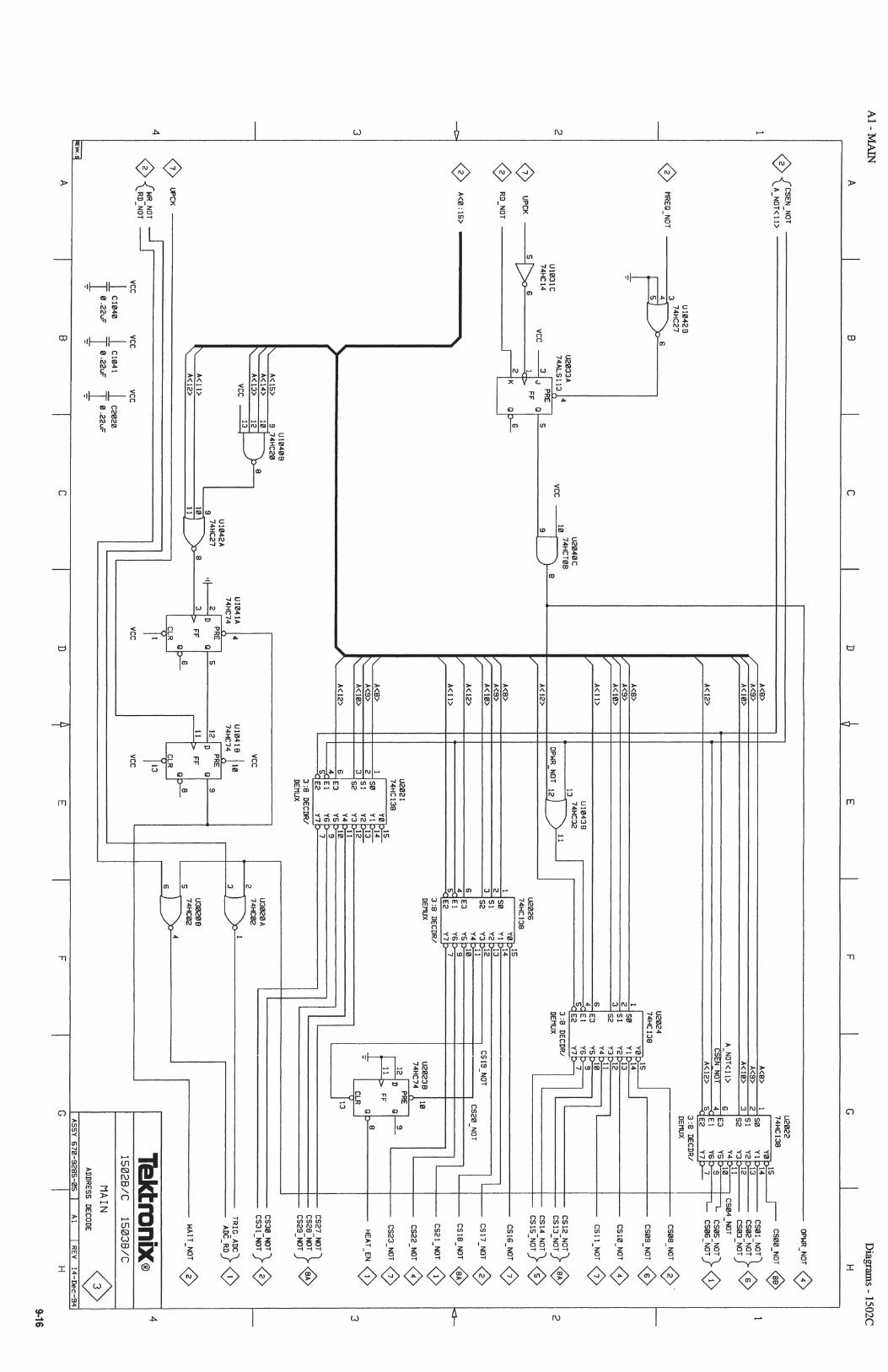


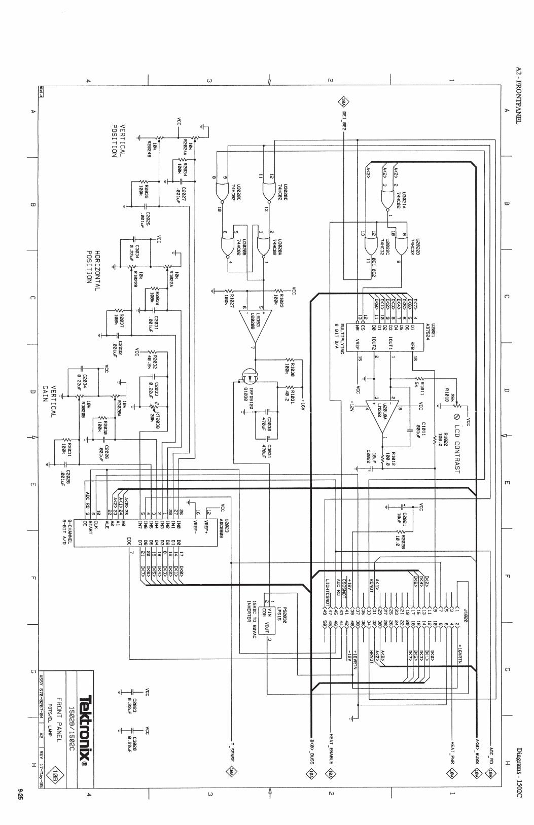


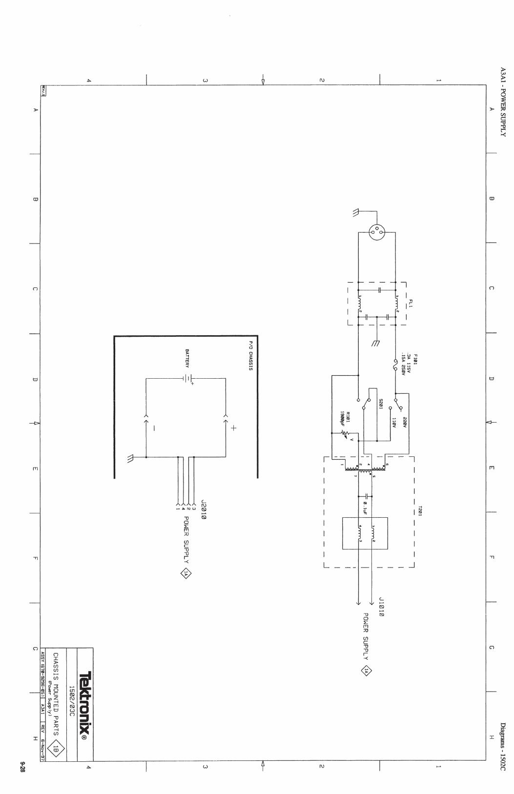


1502C MTDR Service Manual10–1
Replaceable Mechanical Parts
This section contains a list of the replaceable mechanical components for the 1502C.Use this list to identify and order replacement parts.
Parts Ordering InformationReplacement parts are available through your local Tektronix field office orrepresentative.
Changes to Tektronix instruments are sometimes made to accommodate improvedcomponents as they become available and to give you the benefit of the latest circuitimprovements. Therefore, when ordering parts, it is important to include thefollowing information in your order.
Part number
Instrument type or model number
Instrument serial number
Instrument modification number, if applicable
If you order a part that has been replaced with a different or improved part, your localTektronix field office or representative will contact you concerning any change inpart number.
Change information, if any, is located at the rear of this manual.
Using the Replaceable Mechanical Parts ListThe tabular information in the Replaceable Mechanical Parts List is arranged forquick retrieval. Understanding the structure and features of the list will help you findall of the information you need for ordering replacement parts. The following tabledescribes the content of each column in the parts list.

Replaceable Mechanical Parts
10–21502C MTDR Service Manual
Parts List Column Descriptions
Column Column Name Description
1 Figure & Index Number Items in this section are referenced by figure and index numbers to the exploded view illustrationsthat follow.
2 Tektronix Part Number Use this part number when ordering replacement parts from Tektronix.
3 and 4 Serial Number Column three indicates the serial number at which the part was first effective. Column four indicatesthe serial number at which the part was discontinued. No entries indicates the part is good for allserial numbers.
5 Qty This indicates the quantity of parts used.
6 Name & Description An item name is separated from the description by a colon (:). Because of space limitations, an itemname may sometimes appear as incomplete. Use the U.S. Federal Catalog handbook H6-1 forfurther item name identification.
7 Mfr. Code This indicates the code of the actual manufacturer of the part.
8 Mfr. Part Number This indicates the actual manufacturer’s or vendor’s part number.
Abbreviations conform to American National Standard ANSI Y1.1–1972.
Chassis-mounted parts and cable assemblies are located at the end of theReplaceable Electrical Parts List.
The table titled Manufacturers Cross Index shows codes, names, and addresses ofmanufacturers or vendors of components listed in the parts list.
Abbreviations
Chassis Parts
Mfr. Code to ManufacturerCross Index

Replaceable Mechanical Parts
1502C MTDR Service Manual10–3
Manufacturers Cross Index
Mfr.Code Manufacturer Address City, State, Zip Code
TK0588 UNIVERSAL PRECISION PRODUCTS 1775 NW 216TH HILLSBORO, OR 97123
TK0914 WESTERN SINTERING CO INC 2620 STEVENS DRIVE RICHLAND, WA 99352
TK1423 WACHTEL CO INC THE 1100–B L AVENIDA ST MOUNTAIN VIEW, CA 94043
TK1943 NEILSEN MANUFACTURING INC 3501 PORTLAND ROAD NE SALEM, OR 97303
TK2324 RMS COMPANY 7645 BAKER ST NE MINNEAPOOLIS, MN 55432–3421
TK2545 ORNELAS INTERPRISES INC 7275 NW EVERGREEN PKWY #100 HILLSBORO, OR 97124
TK2624 ROSS OPTICAL INDUSTRIES INC 1410 GAIL BORDEN PLACE EL PASO, TX 79935
0J260 COMTEK MANUF OF OREGON PO BOX 4200 BEAVERTON ,OR 97076–4200
0J4C1 TVT DIECASTING AND MFG INC 7330 SW LANDMARK LANE PORTLAND, OR 97223
0DWW6 MICRO PWER ELECTRONICS 7973 SW CIRRUS DRIVE,BLDG. #22 BEAVERTON, OR 97005
0J4Z2 PRECISION PRINTERS 165 SPRINGHILL DRIVE GRAND VALLEY, CA 95945
0J7N9 MCX INC 30608 SAN ANTONIO ST HAYWARD, CA 94544
OJ9P4 DELTA ENGINEERING 19500 SW TETON TUALATIN, OR 97062
0JR05 TRIQUEST CORP 3000 LEWIS AND CLARK HWY VANCOUVER, WA 98661–2999
0JRZ5 GASKET TECHNOLOGY 478 NE 219TH AVENUE TROUTDALE, OR 97060
OKB01 STAUFFER SUPPLY 810 SE SHERMAN PORTLAND, OR 97214
0KB05 NORTH STAR NAMEPLATE 5750 NE MOORE COURT HILLSBORO, OR 97124–6474
00779 AMP INC 2800 FULLING MILL PO BOX 3608 HARRISBURG, PA 17105
06915 RICHCO PLASTIC CO 5825 N TRIPP AVE CHICAGO, IL 60646–6013
22526 BERG ELECTRONICS INC 825 OLD TRAIL RD ETTERS, PA 17319
04963 MINNESOTA MINING AND MFG CO 3M CENTER ST PAUL, MN 55101–1428
28334 3–D POLYMERS 13026 NORMANDIE AVE GARDENA, CA 90249–2126
2K262 BOYD CORP 6136 NE 87TH AVE PO BOX 20038 PORTLAND, OR 97220
2X013 MCGUIRE BEARING CO 947 SE MARKET ST PORTLAND, OR 97214–3556
53387 MINNESOTA MINING MFG CO PO BOX 2963 AUSTIN, TX 78769–2963
58474 SUPERIOR ELECTRIC CO THE 383 MIDDLE ST BRISTOL, CT 06010–7438
5H194 AIR–OIL PRODUCTS CORP 2400 E BURNSIDE PORTLAND, OR 97214–1752
5Y400 TRIAX METAL PRODUCTS INC 1800 216TH AVE NW HILLSBORO, OR 97124–6629
61935 SCHURTER INC 1016 CLEGG COURT PETALUMA, CA 94952–1152
73893 MICRODOT INC 50631 E RUSSELL SCHMIDT BLVD MT CLEMENS, MI 48045
7X318 KASO PLASTICS INC 11015 A NE 39TH VANCOUVER, WA 98662
80009 TEKTRONIX INC 14150 SW KARL BRAUN DR PO BOX 500 BEAVERTON, OR 97077–0001
85471 BOYD CORP 13885 RAMONA AVE CHINO, CA 91710
91094 ESSEX GROUP INC SUFLEX/IWP DIV BAY RD NEWMARKET, NH 03857–9601
91836 KINGS ELECTRONICS CO INC 40 MARBLEDALE ROAD TUCKAHOE, NY 10707–3420
98291 ITT CANNON RF PRODUCTS 585 E MAIN ST NEW BRITAIN, CT 06051

Replaceable Mechanical Parts
10–41502C MTDR Service Manual
Replaceable Mechanical Parts List
Fig. &IndexNumber
Tektronix PartNumber
Serial No.Effective
Serial No.Discont’d Qty Name & Description
Mfr.Code Mfr. Part Number
FIG. 10-1 CABINET
650–3676–00 1 COVER,LID ASSY:LID/COVER ASSEMBLY 7X318 650–3676–00
–1 105–0684–01 2 . LATCH ASSEMBLY: 0J4C1 105–0684–01
–2 213–0839–00 2 . SCR,TPG,TF:4–24 X 0.5 L,FLH,POZ 0KB01 213–0839–00
–3 214–0787–00 1 . STEM,LATCH:ACCESS BOX 7X318 1082
–4 204–0282–00 1 . BODY LATCH:ACCESS BOX,DELRIN 7X318 1267
–5 214–2389–00 2 . PIN,ACTUATOR:POWER SWITCH TK0588 214–2389–00
–6 334–9302–00 1 MARKER,IDENT:MARKED TEKTRONIX 0J4Z2 334–9302–00
–7 062–9363–00 1 CARD,INFO:QUICK REFERENCE 0J4Z2 062–9363–00
–8 334–7475–00 1 MARKER,IDENT:MARKED 1502C 0KB05 334–7475–00
334–8896–00 1 MARKER,IDENT:VOLTAGE WARNING LABEL 0KB05 334–8896–00
650–3677–00 1 CABINET ASSY:BUCKET/HANDLE ASSEMBLY 7X318 650–3677–00
–9 200–1805–00 2 . COVER,HDL LATCH: 0JR05 200–1805–00
–10 213–0739–00 2 . SCR,MACH:10–32 X 0.375,HEX HD,SSTW/NYLON OKB01 213–0739–00
–11 210–1231–00 2 . WSHR,SHLDR:0.82 X 0.9 X 0.07,FBR 0KB01 210–1231–00
–12 386–3303–01 2 . PLATE,SECURING:HANDLE,STEEL TK1943 386–3303–01
–13 107–0035–00 4 . DISC,FRICTION:0.38 X 1.865 X 0.031,ASB 2K262 107–0035–00
–14 210–1501–00 B021236 4 . WSHR,FRICTION:1.820 X 0.388,304SS 20GA 0J9P4 210–1501–00
–15 367–0204–01 B020000 B021235 1 . HANDLE,CARRY:11.7 L,BLK VINYL W/HDW 0J9P4 367–0204–01
367–0449–00 B021236 1 . HANDLE,CARRY:BLACK VINYL, 302 SST 0J9P4 367–0449–00
–16 131–1705–01 1 . CONN,RCPT,ELEC:POWER INTERCONNECT 7X318 131–1705–01
–17 213–0012–00 2 . SCREW,TPG,TC:4–40 X 0.375,TYPE T,FLH 100 DEG 73893 ORD BY DESCR
–18 348–0419–00 2 . FOOT,CABINET:FRONT,BLK POLYURETHANE 7X318 1046
–19 211–0507–00 4 . SCR,MACH:6–32 X 0.312,PNH,POZ 0KB01 211–0507–00
–20 348–0420–01 2 . FOOT,CABINET:REAR,BLK POLYURETHANE 7X318 1048
–21 213–0451–02 4 . SCR,EXT,RLV:10–24 X 1.75,SST,PSVT 0KB01 213–0451–02
–22 354–0175–00 4 . RING,RTNG:TYPE E EXT,U/O 0.188 2X013 1000–18–ST–CD
–23 213–0183–00 2 . SCR,TPG,TF:6–20 X 0.5,TYPEB,PNH,POZ 0KB01 213–0183–00
–24 348–0444–00 4 . SEAL,BOLT:0.186 X 0.443,0.05 THK 80009 348–0444–00
–25 386–4704–00 2 . PLATE,REINF:3.8 X 0.434,STL 7X318 386–4704–00
–26 334–7662–02 1 . MARKER,IDENT:MKD REMOVE COVER TO; & W/VOLT INFO 0KB05 334–7662–02
–27 200–3805–00 1 . COVER,FUSE:VOLTAGE SELECT,PC,CLEAR 0JR05 200–3805–00
–28 214–4276–00 2 . THUMBSCREW:6–32 X 0.50,0.317 OD,SST TK2324 214–4276–00
–29 348–1167–00 1 . GASKET:FUSE & VOLTAGE SELECT COVER 0JRZ5 348–1167–00

Replaceable Mechanical Parts
1502C MTDR Service Manual10–5
Replaceable Mechanical Parts List (Cont.)
Fig. &IndexNumber Mfr. Part Number
Mfr.CodeName & DescriptionQty
Serial No.Discont’d
Serial No.Effective
Tektronix PartNumber
FIG. 10-2. FRAME AND FRONT PANEL
–1 366–2097–00 4 SHELL,KNOB:DOVE GRAY,0.060 X 0.375 7X318 1076
–2 366–2104–00 1 KNOB:SET REF/W DOT SET FOR 90 7X318 1078
–3 366–2098–00 2 SHELL,KNOB:DOVE GRAY W/INDEX DOT 7X318 1077
EACH KNOB INCLUDES:
213–0153–00 1 . SETSCREW:5–40 X 0.125,STL,HEX SKT 0KB01 ORDER BY DESCR
–4 131–4178–00 1 CONN,RCPT,ELEC:BNC,FEMALE SHORTING 91836 752–17–9
–5 650–3697–00 1 DUST COVER ASSEMBLY W/STRAP 7X318 650–3697–00
––––– ––––– 1 SWITCH,ROTARY (SEE A2S3012 REPL)
––––– ––––– 1 RESISTOR,VARIABLE (SEE A2R3020 REPL)
––––– ––––– 1 SWITCH ROTARY (SEE A2S3020 REPL)
––––– ––––– 1 SWITCH ROTARY (SEE A2S3021 REPL)
––––– ––––– 1 SWITCH ROTARY (SEE A2S3022 REPL)
––––– ––––– 1 SWITCH ROTARY (SEE A2S3023)
––––– ––––– 1 RESISTOR,VARIABLE (SEE A2R2024 REPL)
––––– ––––– 1 RESISTOR,VARIABLE (SEE A2R1022 REPL)
EACH SWITCH AND VARIABLE RESISTOR INCLUDES:
–6 210–0583–00 1 . NUT,PLAIN HEX:0.25–32 X 0.312 0KB01 210–0583–00
–7 210–0940–00 1 . WSHR,FLAT:0.25 X 0.375 X 0.02,STL CD PL 0KB01 210–0940–00
EACH VARIABLE RESISTOR INCLUDES:
–8 354–0581–00 1 . O–RING:0.25 X 0.062 OD XSECT 5H194 2–010–S455–70
–9 348–1145–01 . SEAL,CONT SHAFT:0.125 X 0.187 OD X 0.3 L 80009 348–1145–01
–10 366–0655–05 1 PUSH BUTTON:MENU,0.523 X 0.253 0JR05 366–0655–05
–11 366–0655–01 1 PUSH BUTTON:VIEW INPUT 0JR05 366–0655–01
–12 366–0655–02 1 PUSH BUTTON:VIEW STORE 0JR05 366–0655–02
–13 366–0655–03 1 PUSH BUTTON:VIEW DIFF 0JR05 366–0655–03
–14 366–0655–04 1 PUSH BUTTON:STORE 0JR05 366–0655–04
–15 334–7111–01 1 MARKER,IDENT:MARKED 1502C 0KB05 334–7111–01
–16 213–1089–00 4 SCREW,TYPE–F:6–32 X .500,FLH,POS,410 SS OKB01 213–1089–00
–17 614–0389–01 1 FRONT PANEL ASSEMBLY 80009 614–0389–01
–18 348–0477–00 1 . SEAL,RBR STRIP:0.94W X 0.062THK X 28.0L 2K262 R–10460

Replaceable Mechanical Parts
10–61502C MTDR Service Manual
Replaceable Mechanical Parts List (Cont.)
Fig. &IndexNumber Mfr. Part Number
Mfr.CodeName & DescriptionQty
Serial No.Discont’d
Serial No.Effective
Tektronix PartNumber
FIG. 10-2. FRAME AND FRONT PANEL (Con’t)
–19 348–0477–00 1 . SEAL,RBR STRIP:0.94W X 0.062THK X 28.0L 2K262 R–10460
–20 348–1144–00 1 . GASKET,COND:ELASTOMER W/AL 0JRZ5 348–1144–00
–21 348–0920–00 1 . SHLD GSKT,ELEC:PUSH BUTTON 28334 348–0920–00
–22 331–0502–00 1 . WINDOW,DSP,PORT:2.335 X 4.357 X 0.125,GLASS TK2624 331–0502–00
–23 ––––– ––––– 1 CKT BD ASSY:FRONT PANEL (SEE A2 REPL)
–24 211–0658–00 4 SCR,ASSEM WSHR:6–32 X 0.312,PNH,POZ 0KB01 211–0658–00
–25 ––––– ––––– AR . CONN,HDR:PCB,MALE (SEE A2 REPL)
–26 131–0993–00 1 . . BUS CONDUCTOR:SHUNT/SHORTING,FEMALE 22526 65474–006
–27 ––––– ––––– 1 . CONN,HDR:PCB,MALE (SEE A2 REPL)
–28 342–0731–00 1 INSULATOR:FISHPAPER,3.6 X 3.0 80009 342–0731–00
–29 ––––– ––––– 1 DISPLAY MODULE:(SEE A5 REPL)
–30 220–0407–00 4 NUT,SLFLKG,HEX:6–32 X 0.312 HEX 0KB01 220–0407–00
–31 337–2193–05 2 SHIELD,ELEC:EMI,BOTTOM TK1943 337–2193–05
211–0661–00 7 SCR,ASSEM WSHR:4–40 X 0.25,PNH,POZ 0KB01 211–0661–00
129–1092–00 1 SPACER,POST:0.605 L,4–40,HEX 58474 BP21BLACK
210–1307–00 1 WHSR,LOCK:0.115 ID,SPLIT 0KB01 210–1307–00
210–1002–00 1 WSHR,FLAT:0.125 X 0.25 OD X 0.022 0KB01 210–1002–00
334–8135–00 1 MKR,IDENT:MKD EMI SHIELD INSTRU 0J4Z2 334–8135–00
(NOT ILLUSTRATED AT THIS TIME)
–32 650–3714–00 1 ON/OFF SHAFT ASSEMBLY TK2545 650–3714–00
–33 220–0961–00 1 NUT BLOCK:6–32 X 0.438,AL,CHROMATE 5Y400 220–0961–00
–34 213–0966–00 1 . SETSCREW:6–32 X 0.188 HEX,W/NYLON 80009 213–0966–00
NOTE: THE FOLLOWING FOUR COMPONENTS ARESUBPARTS OF THE CHASSIS ASSEMBLY
–35 211–0005–00 3 . SCR,MACH:4–40 X 0.125,PNH,POZ 0KB01 211–0005–00
–36 210–0851–00 3 . WSHR,FLAT:0.119 X 0.375 OD X 0.025 0KB01 210–0851–00
–37 105–0954–01 1 . LEVER:3.25L X 0.5W X 0.05,AL 80009 105–0954–01
–38 384–1674–01 1 . EXTENSION SHAFT:7.59 L X 0.5,AL 80009 384–1674–01
–39 650–3699–00 1 CHART EXTRUSION ASSEMBLY 0J7N9 650–3699–00
–40 212–0001–00 2 SCR,MACH:8–32 X 0.25,PNH,POZ 0KB01 212–0001–00
–41 210–0008–00 2 WSHR,LOCK:#8,INTL,0.02 THK 0KB01 ORD BY DESCR
–42 210–0458–00 1 NUT,PL,ASSEM WA:8–32 X 0.344 0KB01 ORD BY DESCR
–43 ––––– ––––– 1 CA ASSY: (SEE WIRE ASSEMBLIES)

Replaceable Mechanical Parts
1502C MTDR Service Manual10–7
Replaceable Mechanical Parts List (Cont.)
Fig. &IndexNumber Mfr. Part Number
Mfr.CodeName & DescriptionQty
Serial No.Discont’d
Serial No.Effective
Tektronix PartNumber
FIG. 10-2. FRAME AND FRONT PANEL (Con’t)
200–3737–00 1 COVER,FRONT:OPTION PORT 0J9P4 200–3737–00
COVER PORT INCLUDES:
–44 200–3451–01 . COVER,PORT: 5Y400 200–3451–01
–45 348–1118–01 1 . GASKET:OPTION PORT COVER,0.062 THK 0JRZ5 348–1118–01
–46 105–0959–01 1 . LCH,OPT PORT COVER:STEEL,ZINC PLATE TK1423 DZUSDP109SMOD
–47 407–3675–00 1 . FRAME:OPTION PORT COVER 0J9P4 407–3675–00
–48 213–0123–00 2 . SCR,TPG,TF:6–32 X 0.375,FLH100 DEG,POZ 0KB01 ORD BY DESCR
–49 650–3742–00 1 COVER,GASKET ASSY:RANGE BOARD 0J9P4 650–3742–00
–50 211–0661–00 2 SCR,ASSEM WSHR:4–40 X 0.25,PNH,POZ 0KB01 211–0661–00
–51 ––––– ––––– 1 CKT BD ASSY: (SEE A4 REPL)
–52 131–0391–00 1 . CONN,RF JACK:SMB,50 OHM 98291 051–051–0049
–53 131–3360–00 1 . CONN,HDR:PCB,MALE,SHRD/4SIDES 53387 N2520–6002UB
–54 441–1683–00 1 CHASSIS,FRONT:ALNOTE: FRONT CHASSIS IS A SUBPART TO CHASSIS ASSY
0J260 441–1683–00
–55 211–0661–00 2 SCR,ASSEM WSHR:4–40 X 0.25,PNH,POZ 0KB01 211–0661–00
210–1307–00 2 WSHR,LOCK:0.115 ID,SPLIT 0KB01 ORD BY DESCR
–56 211–0007–00 1 SCR,MACH:4–40 X 0.188,PNH,POZ 0KB01 211–0007–00
–57 210–1307–00 B021764 1 WSHR,LOCK:0.115 ID,SPLIT 0KB01 ORD BY DESCR
–58 351–0755–00 4 GUIDE,CKT BD:POLYCARBONATE,2.5 LNOTE: CKT BD GUIDES ARE SUBPARTS OF CHASSIS ASSY
06915 TCG1–2.500–03
–59 210–0586–00 1 NUT,PL,ASSEM W:4–40 X 0.25 0KB01 ORD BY DESCR
–60 ––––– ––––– 1 POWER SUPPLY ASSY: (SEE A3 REPL)
–61 211–0007–00 1 SCR,MACH:4–40 X 0.188,PNH,POZ 0KB01 211–0007–00
211–0105–00 1 SCR,MACH:4–40 X 0.188,FLH,POZ 0KB01 ORD BY DESCR
211–0661–00 1 SCR,ASSEM WSHR:4–40 X 0.25,PNH,POZ 0KB01 211–0661–00
–62 211–0198–00 2 SCR,MACH:4–40 X 0..438,PNH,POZ 0KB01 211–0198–00
–63 210–0005–00 1 WSHR,LOCK:#6 EXT,0.02 THK,STL,CD PL 0KB01 210–0005–00
–64 ––––– ––––– 1 CKT BD ASSY: (SEE A1 REPL)
–65 211–0661–00 9 SCR,ASSEM WSHR:4–40 X 0.25,PNH,POZ 0KB01 211–0661–00
–66 131–3361–00 1 . CONN,HDR:PCD,MALE,RTANG W/SHRD 53387 2526–5002UB
–67 131–3181–00 1 . CONN,HDR:PCB,MALE,RTANG W.SHRD 53387 2540–5002UB
–68 131–3359–00 1 . CONN,HDR:PCB,MALE,2 X 10 53387 2520–5002UB
–69 136–0755–00 1 . SKT,DIP:FEMALE,2 X 14 00779 2–641605–3
–70 131–4183–00 1 . CONN,HDR:PCB,MALE,2 X 7 53387 2514–6002UB

Replaceable Mechanical Parts
10–81502C MTDR Service Manual
Replaceable Mechanical Parts List (Cont.)
Fig. &IndexNumber Mfr. Part Number
Mfr.CodeName & DescriptionQty
Serial No.Discont’d
Serial No.Effective
Tektronix PartNumber
FIG. 10-2. FRAME AND FRONT PANEL (Con’t)
–71 213–0904–00 4 SCR,TPG,TR:6–32 X 0.5 PNH,TORX 0KB01 213–0904–00
–72 ––––– ––––– 1 CHASSIS,MAIN:AL (SEE PWR SUPPLY ASSY) 0J9P4 650–2183–02
040–1276–01 BATTERY ASSY 80009 040–1276–01
–73 343–1436–00 1 . CLAMP,BTRY MT:ALUMINUM 0J260 343–1436–00
–74 212–0001–00 2 . SCREW,MACH:8–32 X 0.25,PNH,STL CD PL,POZ 0KB01 212–0001–00
–75 210–0007–00 2 . WSHR,LOCK:#8 EXT,0.02 THK,CD PL STL 0KB01 ORD BY DESCR
–76 348–0090–00 3 . PAD,CUSHIONING:2.03 X 0.69 X 0.312 SI RBR 85471 R–1047OMED/PSA
–77 146–0066–00 1 . BATTERY:12V LEAD ACID,3.4AH,5.28 X 2.36 X 2.6 RECT 0DWW6 LCR–12V3.4P
––––– ––––– 1 . CA ASSY:(SEE WIRE ASSYS)

Replaceable Mechanical Parts
1502C MTDR Service Manual10–9
Replaceable Mechanical Parts List (Cont.)
Fig. &IndexNumber Mfr. Part Number
Mfr.CodeName & DescriptionQty
Serial No.Discont’d
Serial No.Effective
Tektronix PartNumber
FIG. 10-3 650–3715-01 POWER SUPPLY MODULE
–1 ––––– ––––– 1 CKT BD ASSY:( SEE A3A1 REPL)
–2 211–0661–00 4 SCR,ASSEM WSHR:4–40 X 0.25,PNH,POZ 0KB01 211–0661–00
–3 131–3445–00 1 . CONN,HDR:MALE,RTANG,2 X 7 53387 2514–5002UB
–4 131–4177–00 AR . CONN,HDR:MALE,STR,1 X 31 W/INSUL 22562 65576–131
–5 131–1857–00 AR . CONN,HDR:MALE,STR,1 X 36 22526 65507–B6
––––– ––––– 1 . XSTR: (SEE CHASSIS MOUNTED PARTS)
–6 211–0507–00 1 . SCR,MACH:6–32 X 0.312,PNH,POZ 0KB01 211–0507–00
–7 210–0561–00 1 . NUT,PL,HEEX:6–32 X 0.188 0KB01 210–0561–00
––––– ––––– 1 . IC: (SEE A3A1U2010 REPL)
–8 211–0507–00 1 . SCR,MACH:6–32 X 0.312,PNH,POZ 0KB01 211–0507–00
–9 210–0561–00 1 . NUT,PL,HEX:6–32 X 0.188 0KB01 210–0561–00
253–0188–00 1 . TAPE,PRESS SENS:URETHANE FOAM 24963 4008 3/4
162–0503–00 AR . INSUL SLVG,ELEC:0.042 ID/ACRYLIC/FBRGLASS 91094 ORD BY DESCR
650–3715–01 POWER SUPPLY ASSEMBLY WITH CHASSIS MOUNTEDELECTRICAL PARTS
0J7N9 650–3715–01
–10 220–0547–01 4 . NUT BLOCK:4–40 X 0.282 TK0914 ORD BY DESCR
–11 211–0105–00 4 . SCR,MACH:4–40 X 0.188,FLH,POZ 0KB01 211–0105–00
–12 ––––– ––––– 1 . CHASSIS,PWR SUPPLY:SIDE
–13 211–0105–00 3 . SCR,MACH:4–40 X 0.188,FLH,POZ OKB01 211–0105–00
–14 120–1607–00 B020000 B021232 1 . A3T201 XFMR: PWR,115/230VAC,50/60HZ 08779 DP241–6–24
120–1922–00 B021233 1 . A3T201 XFMR: PWR,115/230VAC,50/60HZ 0JR03 Z–91260A
307–0449–00 1 . A3R101 RES, V SENSITIVE:1900PF,100A,130V 34371 V130LA20A
–15 212–0112–00 2 . SCR,MACH:8–32 X 0.188,TRH,SST,POZ 0KBO1 ORD BY DESCR
–16 210–0002–00 2 . WSHR,LOCK:#8 EXT,0.02 THK 0KBO1 ORD BY DESCR
–17 260–2372–00 1 . A3S201 SWITCH,ROTARY: 61935 033–4501
–18 204–0832–00 1 . BODY,FUSEHLDR:3AG & 5 X 20MM FUSES 61935 031 1673
159–0029–01 1 . A3F101 FUSE CARTRIDGE:BUSSMAN ONLY 71400 MDL3/10
159–0054–00 1 . A3F101 FUSE CARTRIDGE:3AG,0.15A,250V 71400 MDL 15/100
–19 200–2264–00 1 . CAP,FUSEHLDR:3AG FUSES,SFTY CONTROL 61935 FEK 031 1666
–20 119–3488–00 1 . A3FL1 FILTER,RFI: 1A,115/230VAC,50/60HZ 0GV52 FN328–1/01
–21 211–0101–00 2 . SCR,MACH:4–40 X 0.25,FLH,100 DEG,POZ 0KB01 ORD BY DESCR
–22 210–0202–00 1 . TERMINAL,LUG:0.146 ID,LOCKING 0KB01 210–0202–00
–23 211–0658–00 1 . SCR,ASSEM,WA:6–32 X 0.312,PNH,POZ 0KB01 211–0658–00
–24 ––––– ––––– 1 . CHASSIS,PWR SUPPLY:
334–3379–01 1 . MARKER,IDENT:MKD GROUND SYMBOL 0KB05 334–3379–01
Replaceable Mechanical Parts
10–101502C MTDR Service Manual
Replaceable Mechanical Parts List (Cont.)
Fig. &IndexNumber Mfr. Part Number
Mfr.CodeName & DescriptionQty
Serial No.Discont’d
Serial No.Effective
Tektronix PartNumber
POWER CORD OPTIONS
161–0066–00 1 CA ASSY,PWR:3,18 AWG,250V/10A,98INCH,STR,IEC320,RCPT X NEMA 5–15P,US,
0B445 ECM–161–0066–00
161–0066–10 1 CA ASSY,PWR:3,1.0 MM SQ,250V/10A,2.5METER,STR,IEC320,RCPT X 13A,FUSED UK PLUG(13AFUSE),UNI
TK2541 ORDER BYDESCRIPTION
161–0066–11 1 CA ASSY,PWR:3,1.0MM SQ,250V/10A,2.5METER,STR,IEC320,RCPT,AUSTRALIA,
80126 ORDER BYDESCRIPTION
161–0066–12 1 CA ASSY,PWR:3,18 AWG,250V/10A,98INCH,STR,IEC320,RCPT X NEMA 6–15P,US,
S3109 ORDER BYDESCRIPTION
161–0154–00 1 CA ASSY,PWR:3,1.0MM SQ,250V/10A,2.5METER,STR,IEC320,RCPT,SWISS,
5F520 86515030
STANDARD ACESSORIES
016–0915–00 1 BATTERY ASSY:1502C/1503C 80009 016–0915–00
159–0029–01 1 FUSE,CARTRIDGE:3AG,0.3A,250V,12 MIN,BUSSMAN ONLY, 71400 MDL3/10
159–0054–00 1 FUSE,CARTRIDGE:3AG,0.15A,250V,25SEC 71400 MDL 15/100
161–0228–00 1 CABLE ASSY,PWR:3,18 AWG,98 L,SJTWA,BLK,60 DEGC,MC–6–3C X STR,BME,10A/125V,
TK6372 FH49061
200–3737–00 1 COVER,FRONT:OPTION PORT 0J260 PER TEKDOCUMENTATION
012–1350–00 1 CABLE,INTCON:50 OHM,3 FEET L,W/STR RELIEF TK6159 ASI 65289
011–0123–00 1 TERMN,COAXIAL:50 OHM,BNC,VSWR DC–4GHZ 1.15 64537 T190CS
103–0028–00 1 Adapter, Connec:BNC Female to Female, 1.3 L, Gold/Nickel 24931 28A100–2
003–0700–00 1 SLIDE RULE:TDR TK2233 PER TEKDOCUMENTATION
062–8344–00 1 DATA SHEET:TDR SLIDE RULE APPLICATION NOTE TK2548 PER TEK P/N
016–0814–00 1 POUCH,ACCESSORY:11.5 L X 9.5 W X 1.75 H,VINYL TK2582 PER TEKDOCUMENTATION
070–7169–00 1 MANUAL,TECH:USER,1502C TK2548 070–7169–00

Replaceable Mechanical Parts
1502C MTDR Service Manual10–11
Replaceable Mechanical Parts List
Fig. &IndexNumber
Tektronix PartNumber
Serial No.Effective
Serial No.Discont’d Qty Name & Description
Mfr.Code Mfr. Part Number
OPTIONAL ACCESSORIES
070–7168–00 1 MANUAL,TECH:SERVICE,1502C TDR TK2548 070–7168–00
040–1276–00 1 MOD KIT:150XC OPTION 03 BATTERY INCLUDINGINSTRUCTIONS
80009 040–1276–00
119–3616–00 1 CHART RECORDER:SPLASH PROOF YTIS 54318 YT–1S
006–7647–00 1 PAPER,CHART:THERMAL,YT1,SINGLE (100 FEET) 54318 40952–903
006–7677–00 1 PAPER,CHART:THERMAL,YT1,BOX OF 25 80009 PER TEKDOCUMENTATION
006–7681–00 1 PAPER,CHART:THERMINAL,YT1,BOX OF 100 80009 006–7681–00
103–0029–00 1 Adapter, Connec:BNC Male to Male 24931 28A101–4
013–0261–00 1 ACCESS,ADAPTER:2 WIRE,FEMALE,BNC/W STR RELIEF TOALLIGATOR CLIPS,7.0 L
TK6159 PAMONA #2630
013–0076–01 1 ADAPTER,CONN:BNC TO RETRACTABLE HOOK TIP 05276 MODEL 3788
103–0090–00 1 Adapter, Connec:BNC Female to Dual Banana Plug 05276 1269 ADAPTER
103–0035–00 1 Adapter, Connec:BNC Dual Binding Post 05276 1296
103–0058–00 1 ADAPTER,CONN:N FEMALE TO BNC MALE 91836 KN–99–46
103–0045–00 1 Adapter, Connec:N Male to BNC Female 24931 29 JP104–3
103–0015–00 1 ADAPTER,CONN:BNC TO UHF 24931 29JP100–3
103–0032–00 1 ADAPTER,CONN:BNC MALE TO UHF FEMALE 74868 30429–2
103–0158–00 1 Adapter, Connec:BNC Female to F Series Male 24931 29JP151–1
013–0126–00 1 ADAPTER,CONN:BNC PLUG TO F JACK (BNC MALE TO FTYPE FEMALE)
80009 013–0126–00
017–0063–00 1 ADAPTER,CONN:GR TO TEK CONN,W/PNL MT NUT 03877 0874–9700
017–0064–00 1 ADAPTER,CONN:TYPE BNC TO GR,MALE 57793 ORDER BYDESCRIPTION
011–0102–00 1 TERMN,COAXIAL:75 OHM,BNC 80009 011–0102–00
015–0327–00 1 FILTER,DIR CUR:1502 80009 015–0327–00
017–0091–00* 1 ADPTR,TDR IMPD:50 OHM TO 75 OHM 80009 017–0091–00
017–0092–00* 1 ADPTR,TDR IMPD:50 OHM TO 93 OHM 80009 017–0092–00
017–0090–00* 1 ADPTR,TDR IMPD:50 OHM TO 125 OHM 80009 017–0090–00
* These adapters should be purchased if GR connectors (017–0063–00 and/or 017–0064–00) are purchased.

Replaceable Mechanical Parts
10–121502C MTDR Service Manual
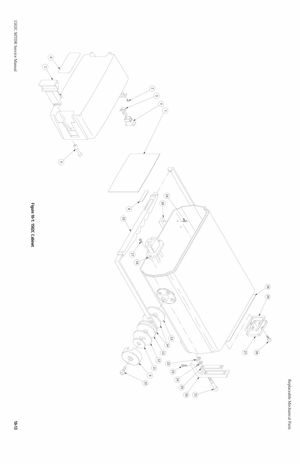
Replaceable M
echanical Parts
10-131502C
MT
DR
Service Manual
1
6
23
47
15
817
16
1819
2629
2827
23
24
2520 21
1314
1312
119
10
5
22
Figure 10-1: 1502C Cabinet

1502
C M
TD
R S
ervi
ce M
anua
l

Replaceable M
echanical Parts
10-151502C
MT
DR
Service Manual
A4
A2
A5
A1
1
29
46
48
4544
5 14 13 12 11 10 16 52
56
57
51
4950
2358
5954
21
2953
22
8
2827
2426
3536
37
6630
25
3433
19
17
15
18
47
32
37
6
6742
68
3169
7264
4140
6362
65
73
7155
7037
3838
43
39
7776
7574
60
614
Figure 10-2: 1502C Frame, Assem
blies and Front Panel Controls
20
A3

1502
C M
TD
R S
ervi
ce M
anua
l
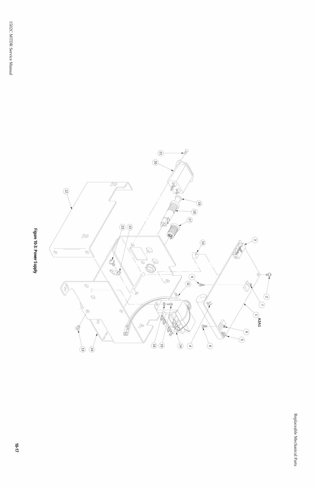
Replaceable M
echanical Parts
10-171502C
MT
DR
Service Manual
Figure 10-3: Power Supply
A3A
13
27
1
95
81516
2413
12
21
20
19
18
17
14 46
10
11
2223

1502
C M
TD
R S
ervi
ce M
anua
l

1502C MTDR Service Manual Glossary–1
Glossary
Imperfections or variations from a desired signal. In TDRs, a pulse of electricalenergy is sent out over the cable. As the pulse-generating circuitry is turned on andoff, the pulse is often distorted slightly and no longer is a perfect step or sine-shapedwaveform.
Alternating current is a method of delivering electrical energy by periodicallychanging the direction of the flow of electrons in the circuit or cable. Even electricalsignals designed to deliver direct current (DC) usually fluctuate enough to have anAC component.
The difference between a measured, generated, or displayed value and the true value.
Electrical conductors that are usually insulated and often shielded. Most cables aremade of metal and are designed to deliver electrical energy from a source (such asa radio transmitter) across a distance to a load (such as an antenna) with minimalenergy loss. Most cables consist of two conductors, one to deliver the electricalsignal and another to act as a return path, which keeps both ends of the circuit atnearly the same electrical potential. In early electrical systems and modern systemsthat over long distances use the earth and/or air as the return path, and the term“ground” or “ground wire” is often used to describe one of the wires in a cable pair.
The amount of signal that is absorbed in the cable as the signal propagates down it.Cable attenuation is typically low at low frequencies and higher at high frequenciesand should be corrected for in some TDR measurements. Cable attenuation isusually expressed in decibels at one or several frequencies. See also: dB and SeriesLoss.
Any condition that makes the cable less efficient at delivering electrical energy thanit was designed to be. Water leaking through the insulation, poorly matedconnectors, and bad splices are typical types cable faults.
(see Reactance)
Cables are designed to match the source and load for the electrical energy that theycarry. The designed impedance is often called the characteristic impedance of thecable. The arrangement of the conductors with respect to each other is the majorfactor in designing the impedance of cables.
Aberrations
AC
Accuracy
Cable
Cable Attenuation
Cable Fault
Capacitance
Characteristic Impedance

Glossary
Glossary–2 1502C MTDR Service Manual
Any substance that will readily allow electricity to flow through it. Good conductorsare metals such as silver, copper, gold, aluminum, and zinc (in that order).
dB is an abbreviation for decibel. Decibels are a method of expressing power orvoltage ratios. The decibel scale is logarithmic. It is often used to express theefficiency of power distribution systems when the ratio consists of the energy putinto the system divided by the energy delivered (or is some cases, lost) by thesystem. Our instrument measures return loss. The formula for decibels is: dB = 2–log (Vi/Vl) where Vi is the voltage of the incident pulse, Vl is the voltage reflectedback by the load, and log is the decimal-based logarithmic function. The dB verticalscale on our instrument refers to the amount of voltage gain (amplification) theinstrument applies to the signal before displaying it. For example, when theinstrument is amplifying the voltage by one hundred, the dB scale would read 40dB, which is 20 log 100.
Direct current is a method of delivering electrical energy by maintaining a constantflow of electrons in one direction. Even circuits designed to generate only AC oftenhave a DC component.
(see Insulation)
A mathematical term that refers to the set of numbers that can be put into a function(the set of numbers that comes out of the function is called the “range”). Atime-domain instrument performs its function by measuring time.
The total opposition to the flow of electrical energy is a cable or circuit. Impedanceis made partly of resistance (frequency independent) and partly of reactance(frequency dependent). Although impedance is expressed in units of ohms, it mustnot be confused with the simple resistance that only applies to DC signals.Technically, impedance is a function of the frequency of the electrical signal, so itshould be specified at a frequency. As a practical matter, the impedance of mostcables changes very little over the range of frequencies they are designed for.
A point in a cable or system where the incident electrical energy is redistributed intoabsorbed, reflected, and/or transmitted electrical energy. The transmitted electricalenergy after the mismatch is less than the incident electrical energy.
The pulse of electrical energy sent out by the TDR. The waveform shown by theTDR consists of this pulse and the reflections of it coming back from the cable orcircuit being tested.
(see Reactance)
Conductor
dB
DC
Dielectric
Domain
Impedance
Impedance Mismatch
Incident Pulse
Inductance

Glossary
1502C MTDR Service Manual Glossary–3
A protective coating on an electrical conductor that will not readily allow electricalenergy to flow away from the conductive part of the cable or circuit. Insulation isalso called dielectric. The kind of dielectric used in a cable determines how fastelectricity can travel through the cable (see Velocity of Propagation).
The short term error or uncertainty in the clock (timebase) of a TDR. If the timingfrom sample to sample is not exact, the waveform will appear to move back and forthrapidly.
An acronym for Liquid Crystal Display. It is the kind of display used on thisinstrument, so the terms display and LCD are often used interchangeably.
rho () is the reflection coefficient of a cable or power delivery system. It is the ratioof the voltage reflected back from the cable or circuit due to cable faults or animpedance mismatch at the load, divided by the voltage applied to the cable.Millirho are thousandths of one rho. Rho measurements are often used to judge howwell the cable is matched to the load at the other end of the cable. If there is an opencircuit in the cable, nearly all the energy will be reflected back when a pulse is sentdown the cable. The reflected voltage will equal the incident pulse voltage and rhowill be +1. If there is a short circuit in the cable, nearly all the energy will bedelivered back to the instrument through the ground or return conductor instead ofbeing sent to the load. The polarity of the reflected pulse will be the opposite of theincident pulse and rho will be –1. If there is no mismatch between the cable and theload, almost no energy will be reflected back and rho will be 0. In general, a loador fault with higher impedance than the cable will return a rho measurement of 0 to+1, and a load or fault with a lower impedance will return a rho measurement of 0to –1. The scale for rho measurements is determined by the height of the incidentpulse. A pulse two divisions high means that each division is 0.5 rho (500 millirho).A pulse set to be four divisions high would make each division 0.25 rho(250 millirho).
Any unwanted electrical energy that interferes with a signal or measurement. Mostnoise is random with respect to the signals sent by the TDR to make a measurementand will appear on the waveform, constantly constantly moving up and down on thedisplay. The NOISE FILTER control sets how many waveforms will be averagedtogether to make the waveform displayed. Noisy waveforms appear to fluctuatearound the real signal. Because it is random, noise will sometimes add to the realsignal and sometimes subtract energy from the real signal. By adding several noisywaveforms together, the noise can be “averaged” out of the signal because theaverage amount of noise adding to the signal will be nearly the same as the averageamount of noise subtracting from the signal. More waveforms in an average aremore likely to approach the real signal (although it takes longer to acquire and addtogether more waveforms).
Insulation
Jitter
LCD
Millirho
Noise

Glossary
Glossary–4 1502C MTDR Service Manual
In a cable, a broken conductor will not allow electrical energy to flow through it.These circuits are also called broken circuits. The circuit is open to the air (whichlooks like a very high impedance).
The statistical spread or variation in a value repeatedly measured, generated, ordisplayed under constant conditions. Also called repeatability.
A conductor’s opposition to the flow of AC electrical energy through it. Allconductors have some reactance. Reactance is made up of capacitance andinductance. Capacitance is the ability of conductors separated by thin layers ifinsulation (dielectric) to store energy between them. Inductance is the ability of aconductor to produce induced voltage when the electrical current through it varies.All conductors have some capacitance and inductance, so all conductors have somereactance, which means they all have impedance.
An instrument that uses reflections to make measurements. Our reflectometers useelectrical energy that is reflected back from points along a cable.
A conductor’s opposition to the flow of DC electrical energy through it. Allconductors have a certain amount of resistance. Resistance is the low (or zero)frequency part of impedance.
For a given parameter, the smallest increment or change in value that can bemeasured, generated, or displayed.
The amount of energy reflected or returned from a cable indicates how much theimpedance in the system is mismatched. The ratio of the energy sent out by the TDR,divided by the energy reflected back, expressed in the logarithmic dB scale, is calledreturn loss.
(see Millirho)
The time it takes a pulse signal to go from 10% to 90% of the change in voltage.
An acronym for Root Mean Squared. RMS is a way of measuring how muchdeviation there is from a known (or desired) waveform. It is also the method usedto calculate how much power is contained in an AC waveform.
Our instruments make measurements by taking a succession of samples in time anddisplaying them as a waveform with voltage on the vertical scale (up and down) and
Open Circuit
Precision
Reactance
Reflectometer
Resistance
Resolution
Return Loss
Rho ()
Risetime
RMS
Sampling Efficiency

Glossary
1502C MTDR Service Manual Glossary–5
time along the horizontal scale (across the display). The circuitry that captures andholds the samples cannot instantly change from one voltage level to another. It mighttake the circuit several samples to settle in at the new voltage after a rapid changein the waveform. How efficiently the circuit moves from one sampled voltage levelto the next is called sampling efficiency. If the efficiency is too low, the waveformswill be smoothed or rounded. If the efficiency is too high (above 100%), the circuitwill actually move beyond the new voltage level in a phenomenon known asovershoot, which becomes an unwanted source of noise in the waveform.
Conductors all have some DC resistance to the flow of electrical energy throughthem. The amount of resistance per unit length is usually nearly constant for a cable.The energy lost overcoming this series resistance is called series loss. The series lossmust be compensated for when measuring the return loss or impedance mismatchat the far end of long cables.
In a cable, a short circuit is a place where the signal conductor comes into electricalcontact with the return path or ground conductor. The electrical circuit is actuallyshorter than was intended. Short circuits are caused by worn, leaky, or missinginsulation.
The change in accuracy of a standard or item of test equipment over an extendedperiod of time. Unless otherwise specified, the period of time is assumed to be thecalibration interval (might also apply to range, resolution, or precision as a functionof time). The term stability might also be used to denote changes resulting fromenvironmental influences, such as temperature, humidity, vibration, and shock.
An acronym for Time-Domain Reflectometer. These instruments are also calledcable radar. They send out pulses of energy and time the interval to reflections. Ifthe velocity of the energy through the cable is known, distances to faults in the cablecan be displayed or computed. Conversely, the speed that the energy travels througha cable of known length can also be computed. The way in which the energy isreflected and the amount of the energy reflected indicate the condition of the cable.
Electrical energy travels at the same speed as light in a vacuum. It travels slower thanthat everywhere else. The speed that it travels in a cable is often expressed as therelative velocity of propagation. This value is just a ration of the speed in the cableto the speed of light (so it is always a number between 0 and 1). A velocity ofpropagation value of 0.50 indicates that the electrical energy moves through thecable at half the speed of light.
(see Noise)
Series Loss
Short Circuit
Stability
TDR
Velocity of Propagation(Vp)
Waveform Averaging

Glossary
Glossary–6 1502C MTDR Service Manual

1502C MTDR Service Manual Index–1
IndexAAccessories, 4–2
Optional, 4–2Standard, 4–2
accessories, standard, 4–2Altitude Spec, 3–3
BBattery (see Power), 1–2Battery Pack Spec, 3–2BNC Connector, 4–2
CCable
Open, 1–14Short, 1–13Test Procedure, 1–13
Distance to Fault, 1–13Horizontal Set Reference, 1–22Reflection Coefficient, 1–15Return Loss, 1–16Store Waveform, 1–18Vertical Set Reference, 1–23View Difference, 1–19View Input, 1–18View Store, 1–19
CalibrationAdjustment Procedure, 6–25
Case/Shield Removal, 6–26Equipment Required, 6–25LCD, 6–36Metric Instruments, 6–25Power Supply, 6–26 ! "# !$ %
Timebase Compensation, 6–25Visual Inspection, 6–26Zero Offset, 6–39
Performance Check, 6–1Chart Recorder, 6–23Display Module, 6–2&' !#
' Equipment Required, 6–1Front Panel, 6–4( $$ $$ $)* $ +#$ +,-$ %
Getting Ready, 6–1Horizontal Scale, 6–7Impedance, 6–35Jitter, 6–21Metric Default, 6–23Metric Instruments, 6–1Noise, 6–13Offset, 6–12Offset/Gain, 6–16Pulse Balance, 6–17RAM/ROM, 6–17Risetime, 6–19Sampling Efficiency, 6–15Timebase, 6–7Vertical Position, 6–12Zero Offset, 6–10
Certifications and Compliances, 3–4Characteristics
Electrical, 3–1Environmental, 3–3Physical, 3–5
Checks (see Performance Checks), 2–1Circuit Description
Display ModuleBlock Diagram, 5–29Column Driver, 5–34# !-+,--++
Column Driver Interface, 5–37Column Drivers, 5–31Controller, 5–36CPU and Display Memory Timing Diagram, 5–39CPU Interface, 5–38EL Backlight, 5–40General, 5–28ITO Heater, 5–40LCD Cell, 5–29Memory, 5–36Memory Interface, 5–38Row Driver, 5–32# !-+,--+

Index
Index–2 1502C MTDR Service Manual
Row Driver Interface, 5–37Row Drivers, 5–31*#.#$+
SBE Cell, 5–30Shift Register, 5–36
Driver/Sampler, 5–23Bridge Bias, 5–24General, 5–23Power Supply Conditioner, 5–24Second Sampler, 5–23Trigger Pulse Shapers, 5–24
Front PanelAnalog-to-Digital Converter, 5–27Block Diagram, 5–26Display Heater, 5–28Display Temperature Compensation, 5–28EL Backlight, 5–27General, 5–25Push Button Switches and Latches, 5–25Resistive Shaft Encoders, 5–27Rotary Binary Switches, 5–27Switch Multiplexers, 5–27
Front-End, 5–23Introduction, 5–1Option Port Interface
Block Diagram, 5–11, 5–13Buffers, 5–12General, 5–10Output Latch, 5–12Supply Control, 5–11Wiring Configuration, 5–12
Power SupplyBattery Charger, 5–6Block Diagram, 5–4DC-to-DC Converter, 5–7Deep Discharge Protection, 5–6General, 5–4Post-Regulator, 5–6Pre-Regulator, 5–5Primary Circuit, 5–5
Processor, Block Diagram, 5–8Processor System
Address Decoding, 5–9Decoding, 5–10Display RAM Space, 5–9Enable and Select Signal space, 5–9EPROM, 5–9General, 5–7Interrupt Logic, 5–10
Memory, 5–9Microprocessor, 5–8Non-volatile RAM Space, 5–9Program Memory, 5–9RAM, 5–9
Pulse Generator/Sampler, Block Diagram, 5–24System Block Diagram, 5–2Timebase
Analog, 5–20Block Diagram, 5–16Calibration of Delay Diagram, 5–19Control Diagram, 5–17Digital, 5–20General, 5–15Time Delay Diagram, 5–18
Video ProcessorGeneral, 5–13Output Scope Waveform, 5–15Summing Amplifier, 5–14Vertical Position DAC, 5–14Video ADC, 5–15Video Amplifier, 5–14
Waveform Accumulation Diagram, 5–3Connectors
BNC – BNC, 4–2BNC to Alligator, 4–2BNC to Banana, 4–2BNC to Binding Post, 4–2BNC to F Type, 4–3BNC to GR, 4–3BNC to Hook Tips, 4–2BNC to N Type, 4–3BNC to UHF, 4–3
ControlsCable Connector, 1–6Distance / Division, 1–6Front Panel, 1–5, 1–6Horizontal Position, 1–7Menu Button, 1–7Noise Filter, 1–6Power, 1–7Store Button, 1–7Velocity of Propagation, 1–7Vertical Position, 1–7Vertical Scale, 1–6View Difference Button, 1–7View Input Button, 1–7View Store Button, 1–7

Index
1502C MTDR Service Manual Index–3
DDepth Spec, 3–5
FFeatures (see Menu), 1–26Fungus Spec, 3–3Fuse, 4–2Fuse (see Power), 1–2
HHandling, 1–1Height Spec, 3–5Horizontal Set Reference, 1–22Humidity Spec, 3–3
IIndicators, 1–6
LLoss, 1–17
MMaintenance
Assembly / Disassembly, (see Removal / Replace-ment), 7–2
Equipment Required, 7–1General, 7–1Metric Default, 7–11Part Removal / Replacement, 7–2
AC Fuse, 7–2Battery, 7–6Case Cover Installaation, 7–19Control Panel, Watertight Seals, 7–17Display Module, Removal, 7–9Front Panel Assembly, Removal, 7–9Front Panel Board-/#%"-/#0-$#.#%
Fuse Holder, Removal, 7–5Main Board&1# -%%'-.%2-/%
Option Port Assembly, Removal, 7–12Power Cord, Conductor Color Code, 7–6
Power Cord Receptacle, Removal, 7–5Power Supply Board, Removal, 7–4Power Supply Module, Removal, 7–3Power Transformer, Removal, 7–5Pulser/Sampler Board, Removal, 7–9Remove Case, 7–3Remove EMI Shields, 7–3Sealing Materials, 7–18Voltage Selector, Removal, 7–5
Preventive, 7–1Cleaning, 7–1Lubrication, 7–2Recalibration, 7–2Visual Inspection, 7–2
Troubleshooting, 7–12Flow Chart, 7–12Waveforms, 7–12When All Else Fails, 7–17
Maximum Hold, 1–26Menu, 1–7, 1–26
Cables, 1–8Diagnostics, 1–9
Chart Recorder, 1–103(#-'
Front Panel, 1–9LCD, 1–9(#-"$"/,$"$$,-"
Service, 1–94$"100$56"(51"*-#&00 .",-)$"
Display Contrast, 1–10Impedance, 1–8Main, 1–7Maximum Hold, 1–26Option Port, 1–10
Debugging, 1–10Diagnostic, 1–10Timing, 1–10
Pulse, 1–27Setup, 1–8
Acquisition Control, 1–8Backlight, 1–8Distance / Division, 1–8Maximum Hold, 1–8Pulse, 1–8Single Sweep, 1–8Vertical Scale, 1–8

Index
Index–4 1502C MTDR Service Manual
Single Sweep, 1–28Velocity of Propagation, 1–8View Stored Waveform, 1–10
NNoise (see also Controls), 1–6
OOhms-at-Cursor, 1–17Open, 1–14Option Port Cover, 4–2Options, 4–1
Chart Recorder (04), 4–1Chart Recorder (07), 4–1Metric Default (05), 4–1Power Cords, 4–1
PPerformance Checks, 2–1
Aberrations, 2–6Conclusions, 2–10Equipment Required, 2–1Horizontal Scale, 2–2Jitter, 2–9Noise, 2–5Offset / Gain, 2–6Risetime, 2–8Sampling Efficiency, 2–6Set Up, 2–2Vertical Position, 2–4
Pouch, 4–2Power
AC Receptacle, 1–1Battery, Low Indicator, 1–4Battery Pack
Care of, 1–2Charging, 1–2
Cords, 4–1Fuse, 1–1Fuse Rating, 1–2Voltage Rating, 1–2Voltage Selector, 1–1Voltages, 1–1
Pulse, 1–27
RReflection Coefficient, 1–15Return Loss, 1–16, 1–17
SSalt Atmosphere Spec, 3–3Sand and Dust Spec, 3–3Scale (see Controls), 1–6Service Manual, 4–2Shock Spec, 3–3Short, 1–13Single Sweep, 1–28Slide Rule, 4–2Specifications, 3–1
Electrical, 3–1Environmental, 3–3Physical, 3–5
Store the Waveform, 1–18
TTemperature, Low, 1–4Terminator, 4–2
VVelocity of Propagation, 1–11
Table of Types, 1–11Unknown Vp, 1–11
Velocity of Propagation (See also Controls), 1–7Vertical Set Reference, 1–23Vibration Spec, 3–3View Difference, 1–19View Input, 1–18View Store, 1–19Voltage (see Power), 1–2Voltage Spec, 3–2Vp (see Velocity of Propagation), 1–11
WWater Resistance Spec, 3–3Waveform Storage, 1–18Weight Spec, 3–5

