15w, 30w, 50w filter-free class-d stereo amplifier family with am
TRANSCRIPT
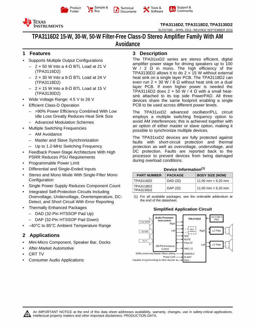
LC Filter
LC FilterLeft
Right
4.5 V-26 VPSU
Tuner AM/FM
CD/ MP3
Aux in
Left
Right
Audio Processor
And controlTPA3116D2
AM/FM Avoidance
Control
FAULTZ
SDZ
MUTE
SyncCapable of synchronizing to other devices
GAIN/SLVGAIN control and Master /Slave setting
AM2,1,0
PLIMITPower Limit
PBTLDetect
Product
Folder
Sample &Buy
Technical
Documents
Tools &
Software
Support &Community
TPA3116D2, TPA3118D2, TPA3130D2SLOS708E –APRIL 2012–REVISED SEPTEMBER 2015
TPA3116D2 15-W, 30-W, 50-W Filter-Free Class-D Stereo Amplifier Family With AMAvoidance
1 Features 3 DescriptionThe TPA31xxD2 series are stereo efficient, digital
1• Supports Multiple Output Configurationsamplifier power stage for driving speakers up to 100– 2 × 50 W Into a 4-Ω BTL Load at 21 V W / 2 Ω in mono. The high efficiency of the
(TPA3116D2) TPA3130D2 allows it to do 2 × 15 W without external– 2 × 30 W Into a 8-Ω BTL Load at 24 V heat sink on a single layer PCB. The TPA3118D2 can
even run 2 × 30 W / 8 Ω without heat sink on a dual(TPA3118D2)layer PCB. If even higher power is needed the– 2 × 15 W Into a 8-Ω BTL Load at 15 VTPA3116D2 does 2 × 50 W / 4 Ω with a small heat-(TPA3130D2) sink attached to its top side PowerPAD. All three
• Wide Voltage Range: 4.5 V to 26 V devices share the same footprint enabling a singlePCB to be used across different power levels.• Efficient Class-D Operation
– >90% Power Efficiency Combined With Low The TPA31xxD2 advanced oscillator/PLL circuitIdle Loss Greatly Reduces Heat Sink Size employs a multiple switching frequency option to
avoid AM interferences; this is achieved together with– Advanced Modulation Schemesan option of either master or slave option, making it• Multiple Switching Frequencies possible to synchronize multiple devices.
– AM AvoidanceThe TPA31xxD2 devices are fully protected against– Master and Slave Synchronization faults with short-circuit protection and thermal
– Up to 1.2-MHz Switching Frequency protection as well as overvoltage, undervoltage, andDC protection. Faults are reported back to the• Feedback Power-Stage Architecture With Highprocessor to prevent devices from being damagedPSRR Reduces PSU Requirementsduring overload conditions.• Programmable Power Limit
• Differential and Single-Ended Inputs Device Information(1)
• Stereo and Mono Mode With Single-Filter Mono PART NUMBER PACKAGE BODY SIZE (NOM)Configuration TPA3116D2 DAD (32) 11.00 mm × 6.20 mm
• Single Power Supply Reduces Component Count TPA3118D2 DAP (32) 11.00 mm × 6.20 mmTPA3130D2• Integrated Self-Protection Circuits Including(1) For all available packages, see the orderable addendum atOvervoltage, Undervoltage, Overtemperature, DC-
the end of the datasheet.Detect, and Short Circuit With Error Reporting• Thermally Enhanced Packages Simplified Application Circuit
– DAD (32-Pin HTSSOP Pad Up)– DAP (32-Pin HTSSOP Pad Down)
• –40°C to 85°C Ambient Temperature Range
2 Applications• Mini-Micro Component, Speaker Bar, Docks• After-Market Automotive• CRT TV• Consumer Audio Applications
1
An IMPORTANT NOTICE at the end of this data sheet addresses availability, warranty, changes, use in safety-critical applications,intellectual property matters and other important disclaimers. PRODUCTION DATA.

TPA3116D2, TPA3118D2, TPA3130D2SLOS708E –APRIL 2012–REVISED SEPTEMBER 2015 www.ti.com
Table of Contents7.3 Feature Description................................................. 131 Features .................................................................. 17.4 Device Functional Modes........................................ 242 Applications ........................................................... 1
8 Applications and Implementation ...................... 253 Description ............................................................. 18.1 Application Information............................................ 254 Revision History..................................................... 28.2 Typical Application .................................................. 255 Pin Configuration and Functions ......................... 3
9 Power Supply Recommendations ...................... 286 Specifications......................................................... 510 Layout................................................................... 286.1 Absolute Maximum Ratings ...................................... 5
10.1 Layout Guidelines ................................................. 286.2 ESD Ratings ............................................................ 510.2 Layout Example .................................................... 296.3 Recommended Operating Conditions....................... 510.3 Heat Sink Used on the EVM ................................. 316.4 Thermal Information .................................................. 6
11 Device and Documentation Support ................. 326.5 DC Electrical Characteristics .................................... 611.1 Related Links ........................................................ 326.6 AC Electrical Characteristics..................................... 611.2 Trademarks ........................................................... 326.7 Typical Characteristics .............................................. 811.3 Electrostatic Discharge Caution............................ 327 Detailed Description ............................................ 1311.4 Glossary ................................................................ 327.1 Overview ................................................................. 13
12 Mechanical, Packaging, and Orderable7.2 Functional Block Diagram ....................................... 13Information ........................................................... 32
4 Revision History
Changes from Revision D (January 2015) to Revision E Page
• Deleted Package DAP (32) from Part Number TPA3116D2 in the Device Information table ............................................... 1
Changes from Revision C (April 2012) to Revision D Page
• Added Pin Configuration and Functions section, ESD Ratings table, Feature Description section, Device FunctionalModes, Application and Implementation section, Power Supply Recommendations section, Layout section, Deviceand Documentation Support section, and Mechanical, Packaging, and Orderable Information section .............................. 1
Changes from Revision B (May 2012) to Revision C Page
• Changed Notes 2 and 3 of the Thermal Information Table. ................................................................................................... 6• Changed the Gain (BTL) Test Condition values for R1 and R2............................................................................................. 6• Changed the Gain (SLV) Test Condition values for R1 and R2............................................................................................. 6• Changed the SYSTEM BLOCK DIAGRAM .......................................................................................................................... 13
2 Submit Documentation Feedback Copyright © 2012–2015, Texas Instruments Incorporated
Product Folder Links: TPA3116D2 TPA3118D2 TPA3130D2
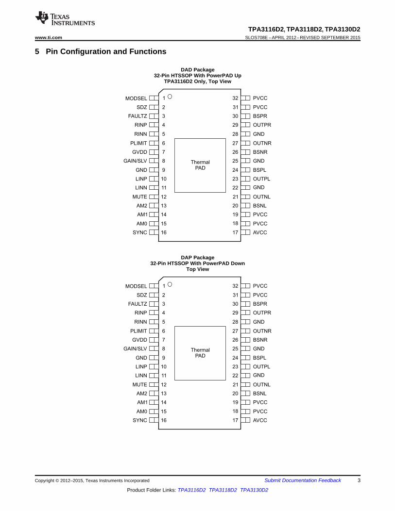
32
31
30
29
19
13
14
15
16 17
18
20
1
2
3
4
5
6
7
8
9
10
11
12 21
22
23
24
28
27
26
25
FAULTZ
SDZ
SYNC
AM0
AM1
MUTE
LINN
LINP
PLIMIT
RINN
GVDD
RINP
AVCC
OUTPR
PVCC
BSPL
GND
OUTPL
PVCC
OUTNL
BSNL
PVCC
OUTNR
BSNR
MODSEL
BSPR
GND
GND
PVCC
GND
GAIN/SLV
AM2
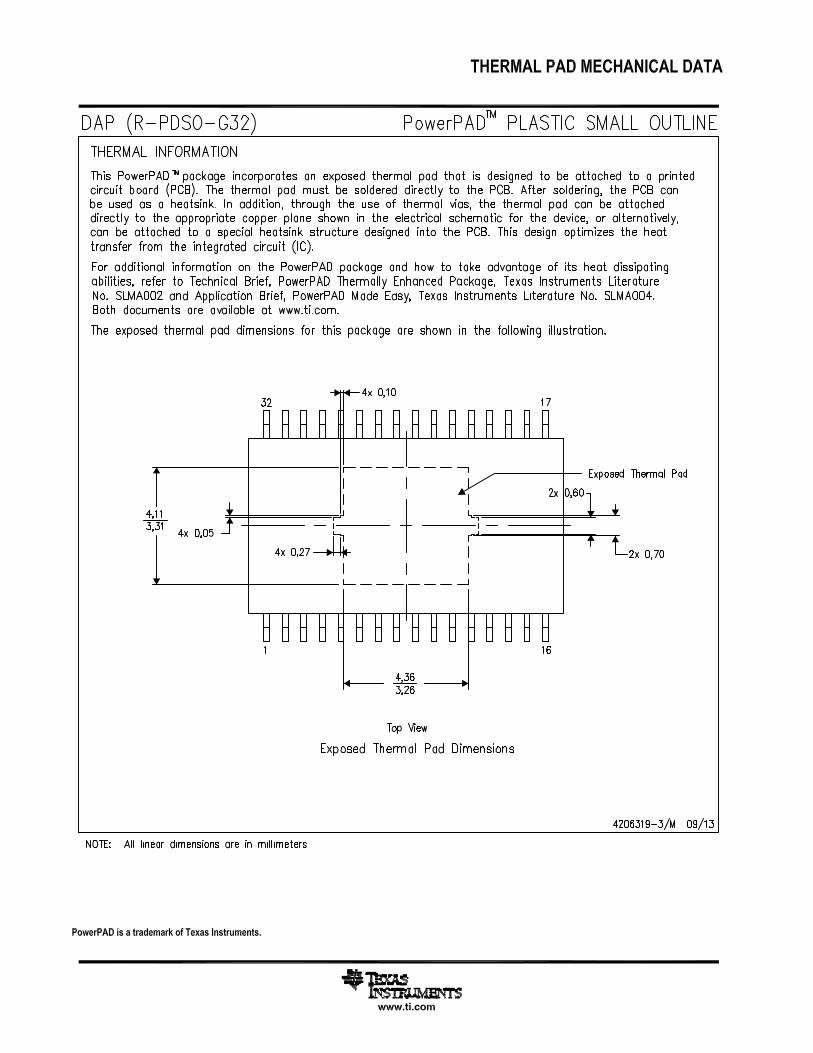
Thermal
PAD
32
31
30
29
19
13
14
15
16 17
18
20
1
2
3
4
5
6
7
8
9
10
11
12 21
22
23
24
28
27
26
25
FAULTZ
SDZ
SYNC
AM0
AM1
MUTE
LINN
LINP
PLIMIT
RINN
GVDD
RINP
AVCC
OUTPR
PVCC
BSPL
GND
OUTPL
PVCC
OUTNL
BSNL
PVCC
OUTNR
BSNR
MODSEL
BSPR
GND
GND
PVCC
GND
GAIN/SLV
AM2
Thermal
PAD
TPA3116D2, TPA3118D2, TPA3130D2www.ti.com SLOS708E –APRIL 2012–REVISED SEPTEMBER 2015
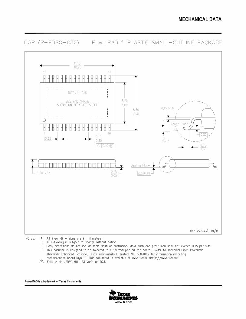
5 Pin Configuration and Functions
DAD Package32-Pin HTSSOP With PowerPAD Up
TPA3116D2 Only, Top View
DAP Package32-Pin HTSSOP With PowerPAD Down
Top View
Copyright © 2012–2015, Texas Instruments Incorporated Submit Documentation Feedback 3
Product Folder Links: TPA3116D2 TPA3118D2 TPA3130D2
TPA3116D2, TPA3118D2, TPA3130D2SLOS708E –APRIL 2012–REVISED SEPTEMBER 2015 www.ti.com
Pin FunctionsPIN
TYPE (1) DESCRIPTIONNO. NAME1 MODSEL I Mode selection logic input (LOW = BD mode, HIGH = 1 SPW mode). TTL logic levels with compliance to
AVCC.2 SDZ I Shutdown logic input for audio amp (LOW = outputs Hi-Z, HIGH = outputs enabled). TTL logic levels with
compliance to AVCC.3 FAULTZ DO General fault reporting including Over-temp, DC Detect. Open drain.
FAULTZ = High, normal operationFAULTZ = Low, fault condition
4 RINP I Positive audio input for right channel. Biased at 3 V.5 RINN I Negative audio input for right channel. Biased at 3 V.6 PLIMIT I Power limit level adjust. Connect a resistor divider from GVDD to GND to set power limit. Connect directly
to GVDD for no power limit.7 GVDD PO Internally generated gate voltage supply. Not to be used as a supply or connected to any component other
than a 1 µF X7R ceramic decoupling capacitor and the PLIMIT and GAIN/SLV resistor dividers.8 GAIN/SLV I Selects Gain and selects between Master and Slave mode depending on pin voltage divider.9 GND G Ground10 LINP I Positive audio input for left channel. Biased at 3 V. Connect to GND for PBTL mode.11 LINN I Negative audio input for left channel. Biased at 3 V. Connect to GND for PBTL mode.12 MUTE I Mute signal for fast disable/enable of outputs (HIGH = outputs Hi-Z, LOW = outputs enabled). TTL logic
levels with compliance to AVCC.13 AM2 I AM Avoidance Frequency Selection14 AM1 I AM Avoidance Frequency Selection15 AM0 I AM Avoidance Frequency Selection16 SYNC DIO Clock input/output for synchronizing multiple class-D devices. Direction determined by GAIN/SLV terminal.17 AVCC P Analog Supply18 PVCC P Power supply19 PVCC P Power supply20 BSNL BST Boot strap for negative left channel output, connect to 220 nF X5R, or better ceramic cap to OUTPL21 OUTNL PO Negative left channel output22 GND G Ground23 OUTPL PO Positive left channel output24 BSPL BST Boot strap for positive left channel output, connect to 220 nF X5R, or better ceramic cap to OUTNL25 GND G Ground26 BSNR BST Boot strap for negative right channel output, connect to 220 nF X5R, or better ceramic cap to OUTNR27 OUTNR PO Negative right channel output28 GND G Ground29 OUTPR PO Positive right channel output30 BSPR BST Boot strap for positive right channel output, connect to 220 nF X5R or better ceramic cap to OUTPR31 PVCC P Power supply32 PVCC P Power supply33 PowerPAD G Connect to GND for best system performance. If not connected to GND, leave floating.
(1) TYPE: DO = Digital Output, I = Analog Input, G = General Ground, PO = Power Output, BST = Boot Strap.
4 Submit Documentation Feedback Copyright © 2012–2015, Texas Instruments Incorporated
Product Folder Links: TPA3116D2 TPA3118D2 TPA3130D2
TPA3116D2, TPA3118D2, TPA3130D2www.ti.com SLOS708E –APRIL 2012–REVISED SEPTEMBER 2015
6 Specifications
6.1 Absolute Maximum Ratingsover operating free-air temperature range (unless otherwise noted) (1)
MIN MAX UNITSupply voltage, VCC PVCC, AVCC –0.3 30 V
INPL, INNL, INPR, INNR –0.3 6.3 VInput voltage, VI PLIMIT, GAIN / SLV, SYNC –0.3 GVDD+0.3 V
AM0, AM1, AM2, MUTE, SDZ, MODSEL –0.3 PVCC+0.3 VSlew rate, maximum (2) AM0, AM1, AM2, MUTE, SDZ, MODSEL 10 V/msOperating free-air temperature, TA –40 85 °COperating junction temperature , TJ –40 150 °CStorage temperature, Tstg –40 125 °C
(1) Stresses beyond those listed under absolute maximum ratings may cause permanent damage to the device. These are stress ratingsonly, and functional operation of the device at these or any other conditions beyond those indicated under recommended operatingconditions is not implied. Exposure to absolute-maximum-rated conditions for extended periods may affect device reliability.
(2) 100 kΩ series resistor is needed if maximum slew rate is exceeded.
6.2 ESD RatingsVALUE UNIT
Human-body model (HBM), per ANSI/ESDA/JEDEC JS-001 (1) ±2000V(ESD) Electrostatic discharge VCharged-device model (CDM), per JEDEC specification JESD22- ±500
C101 (2)
(1) JEDEC document JEP155 states that 500-V HBM allows safe manufacturing with a standard ESD control process.(2) JEDEC document JEP157 states that 250-V CDM allows safe manufacturing with a standard ESD control process. .
6.3 Recommended Operating Conditionsover operating free-air temperature range (unless otherwise noted)
MIN NOM MAX UNITVCC Supply voltage PVCC, AVCC 4.5 26 V
High-level inputVIH AM0, AM1, AM2, MUTE, SDZ, SYNC, MODSEL 2 VvoltageLow-level inputVIL AM0, AM1, AM2, MUTE, SDZ, SYNC, MODSEL 0.8 VvoltageLow-level outputVOL FAULTZ, RPULL-UP = 100 kΩ, PVCC = 26 V 0.8 VvoltageHigh-level inputIIH AM0, AM1, AM2, MUTE, SDZ, MODSEL (VI = 2 V, VCC = 18 V) 50 µAcurrent
TPA3116D2, TPA3118D2 3.2 4RL(BTL) Output filter: L = 10 µH, C = 680 nF
TPA3130D2 5.6 8Minimum load ΩImpedance TPA3116D2, TPA3118D2 1.6RL(PBTL) Output filter: L = 10 µH, C = 1 µF
TPA3130D2 3.2 4Output-filterLo Minimum output filter inductance under short-circuit condition 1 µHInductance
Copyright © 2012–2015, Texas Instruments Incorporated Submit Documentation Feedback 5
Product Folder Links: TPA3116D2 TPA3118D2 TPA3130D2
TPA3116D2, TPA3118D2, TPA3130D2SLOS708E –APRIL 2012–REVISED SEPTEMBER 2015 www.ti.com
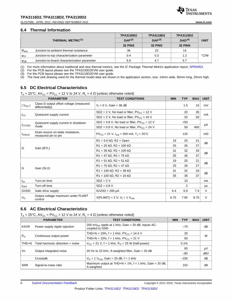
6.4 Thermal InformationTPA3130D2 TPA3118D2 TPA3116D2
THERMAL METRIC (1) DAP (2) DAP (3) DAD (4) UNIT32 PINS 32 PINS 32 PINS
RθJA Junction-to-ambient thermal resistance 36 22 14ψJT Junction-to-top characterization parameter 0.4 0.3 1.2 °C/WψJB Junction-to-board characterization parameter 5.9 4.7 5.7
(1) For more information about traditional and new thermal metrics, see the IC Package Thermal Metrics application report, SPRA953.(2) For the PCB layout please see the TPA3130D2EVM user guide.(3) For the PCB layout please see the TPA3118D2EVM user guide.(4) The heat sink drawing used for the thermal model data are shown in the application section, size: 14mm wide, 50mm long, 25mm high.
6.5 DC Electrical CharacteristicsTA = 25°C, AVCC = PVCC = 12 V to 24 V, RL = 4 Ω (unless otherwise noted)
PARAMETER TEST CONDITIONS MIN TYP MAX UNITClass-D output offset voltage (measured| VOS | VI = 0 V, Gain = 36 dB 1.5 15 mVdifferentially)
SDZ = 2 V, No load or filter, PVCC = 12 V 20 35ICC Quiescent supply current mA
SDZ = 2 V, No load or filter, PVCC = 24 V 32 50SDZ = 0.8 V, No load or filter, PVCC = 12 V <50Quiescent supply current in shutdownICC(SD) µAmode SDZ = 0.8 V, No load or filter, PVCC = 24 V 50 400
Drain-source on-state resistance,rDS(on) PVCC = 21 V, Iout = 500 mA, TJ = 25°C 120 mΩmeasured pin to pinR1 = 5.6 kΩ, R2 = Open 19 20 21
dBR1 = 20 kΩ, R2 = 100 kΩ 25 26 27
G Gain (BTL)R1 = 39 kΩ, R2 = 100 kΩ 31 32 33
dBR1 = 47 kΩ, R2 = 75 kΩ 35 36 37R1 = 51 kΩ, R2 = 51 kΩ 19 20 21
dBR1 = 75 kΩ, R2 = 47 kΩ 25 26 27
G Gain (SLV)R1 = 100 kΩ, R2 = 39 kΩ 31 32 33
dBR1 = 100 kΩ, R2 = 16 kΩ 35 36 37
ton Turn-on time SDZ = 2 V 10 mstOFF Turn-off time SDZ = 0.8 V 2 µsGVDD Gate drive supply IGVDD < 200 µA 6.4 6.9 7.4 V
Output voltage maximum under PLIMITVO V(PLIMIT) = 2 V; VI = 1 Vrms 6.75 7.90 8.75 Vcontrol
6.6 AC Electrical CharacteristicsTA = 25°C, AVCC = PVCC = 12 V to 24 V, RL = 4 Ω (unless otherwise noted)
PARAMETER TEST CONDITIONS MIN TYP MAX UNIT200 mVPP ripple at 1 kHz, Gain = 20 dB, Inputs AC-KSVR Power supply ripple rejection –70 dBcoupled to GNDTHD+N = 10%, f = 1 kHz, PVCC = 14.4 V 25
PO Continuous output power WTHD+N = 10%, f = 1 kHz, PVCC = 21 V 50
THD+N Total harmonic distortion + noise VCC = 21 V, f = 1 kHz, PO = 25 W (half-power) 0.1%65 µV
Vn Output integrated noise 20 Hz to 22 kHz, A-weighted filter, Gain = 20 dB–80 dBV
Crosstalk VO = 1 Vrms, Gain = 20 dB, f = 1 kHz –100 dBMaximum output at THD+N < 1%, f = 1 kHz, Gain = 20 dB,SNR Signal-to-noise ratio 102 dBA-weighted
6 Submit Documentation Feedback Copyright © 2012–2015, Texas Instruments Incorporated
Product Folder Links: TPA3116D2 TPA3118D2 TPA3130D2
TPA3116D2, TPA3118D2, TPA3130D2www.ti.com SLOS708E –APRIL 2012–REVISED SEPTEMBER 2015
AC Electrical Characteristics (continued)TA = 25°C, AVCC = PVCC = 12 V to 24 V, RL = 4 Ω (unless otherwise noted)
PARAMETER TEST CONDITIONS MIN TYP MAX UNITAM2=0, AM1=0, AM0=0 376 400 424AM2=0, AM1=0, AM0=1 470 500 530AM2=0, AM1=1, AM0=0 564 600 636AM2=0, AM1=1, AM0=1 940 1000 1060
fOSC Oscillator frequency kHzAM2=1, AM1=0, AM0=0 1128 1200 1278AM2=1, AM1=0, AM0=1AM2=1, AM1=1, AM0=0 ReservedAM2=1, AM1=1, AM0=1
Thermal trip point 150+ °CThermal hysteresis 15 °C
TPA3130D2 4.5Over current trip point A
TPA3118D2, TPA3116D2 7.5
Copyright © 2012–2015, Texas Instruments Incorporated Submit Documentation Feedback 7
Product Folder Links: TPA3116D2 TPA3118D2 TPA3130D2
0.001
0.01
0.1
1
10
20 100 1k 10k 20kFrequency (Hz)
TH
D+
N (
%)
PO = 1WPO = 5WPO = 10W
Gain = 26dBPVCC = 24VTA = 25°CRL = 8Ω
G006
0.001
0.01
0.1
1
10
0.01 0.1 1 10Output Power (W)
TH
D+
N (
%)
f = 20Hzf = 1kHzf = 6kHz
Gain = 26dBPVCC = 6VTA = 25°CRL = 4Ω
G008
0.001
0.01
0.1
1
10
20 100 1k 10k 20kFrequency (Hz)
TH
D+
N (
%)
PO = 1WPO = 5WPO = 10W
Gain = 26dBPVCC = 24VTA = 25°CRL = 4Ω
G004
0.001
0.01
0.1
1
10
20 100 1k 10k 20kFrequency (Hz)
TH
D+
N (
%)
PO = 1WPO = 2.5WPO = 5W
Gain = 26dBPVCC = 12VTA = 25°CRL = 8Ω
G005
0.001
0.01
0.1
1
10
20 100 1k 10k 20kFrequency (Hz)
TH
D+
N (
%)
PO = 0.5WPO = 1WPO = 2.5W
Gain = 26dBPVCC = 6VTA = 25°CRL = 4Ω
G002
0.001
0.01
0.1
1
10
20 100 1k 10k 20kFrequency (Hz)
TH
D+
N (
%)
PO = 1WPO = 2.5WPO = 5W
Gain = 26dBPVCC = 12VTA = 25°CRL = 4Ω
G003
TPA3116D2, TPA3118D2, TPA3130D2SLOS708E –APRIL 2012–REVISED SEPTEMBER 2015 www.ti.com
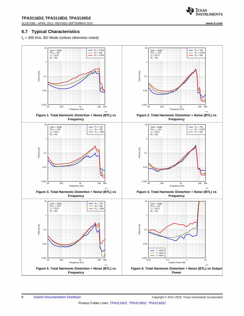
6.7 Typical Characteristicsfs = 400 kHz, BD Mode (unless otherwise noted)
Figure 1. Total Harmonic Distortion + Noise (BTL) vs Figure 2. Total Harmonic Distortion + Noise (BTL) vsFrequency Frequency
Figure 3. Total Harmonic Distortion + Noise (BTL) vs Figure 4. Total Harmonic Distortion + Noise (BTL) vsFrequency Frequency
Figure 5. Total Harmonic Distortion + Noise (BTL) vs Figure 6. Total Harmonic Distortion + Noise (BTL) vs OutputFrequency Power
8 Submit Documentation Feedback Copyright © 2012–2015, Texas Instruments Incorporated
Product Folder Links: TPA3116D2 TPA3118D2 TPA3130D2

0
10
20
30
40
50
0 1 2 3 4PLIMIT Voltage (V)
Out
put P
ower
(W
)
Gain = 26dBTA = 25°CPVCC = 24VRL = 4Ω
G013
20 100 1k 10k 100k−50
−40
−30
−20
−10
0
10
20
30
−500
−400
−300
−200
−100
0
100
200
300
Frequency (Hz)
Gai
n (d
B)
Pha
se (
°)
GainPhase
Gain = 26dBPVCC = 12VTA = 25°CRL = 4Ω
G014
0.001
0.01
0.1
1
10
0.01 0.1 1 10 50Output Power (W)
TH
D+
N (
%)
f = 20Hzf = 1kHzf = 6kHz
Gain = 26dBPVCC = 12VTA = 25°CRL = 8Ω
G011
0.001
0.01
0.1
1
10
0.01 0.1 1 10 50Output Power (W)
TH
D+
N (
%)
f = 20Hzf = 1kHzf = 6kHz
Gain = 26dBPVCC = 24VTA = 25°CRL = 8Ω
G012
0.001
0.01
0.1
1
10
0.01 0.1 1 10 40Output Power (W)
TH
D+
N (
%)
f = 20Hzf = 1kHzf = 6kHz
Gain = 26dBPVCC = 12VTA = 25°CRL = 4Ω
G009
0.001
0.01
0.1
1
10
0.01 0.1 1 10 100Output Power (W)
TH
D+
N (
%)
f = 20Hzf = 1kHzf = 6kHz
Gain = 26dBPVCC = 24VTA = 25°CRL = 4Ω
G010
TPA3116D2, TPA3118D2, TPA3130D2www.ti.com SLOS708E –APRIL 2012–REVISED SEPTEMBER 2015
Typical Characteristics (continued)fs = 400 kHz, BD Mode (unless otherwise noted)
Figure 7. Total Harmonic Distortion + Noise (BTL) vs Output Figure 8. Total Harmonic Distortion + Noise (BTL) vs OutputPower Power
Figure 9. Total Harmonic Distortion + Noise (BTL) vs Output Figure 10. Total Harmonic Distortion + Noise (BTL) vsPower Output Power
Figure 11. Output Power (BTL) vs Plimit Voltage Figure 12. Gain/Phase (BTL) vs Frequency
Copyright © 2012–2015, Texas Instruments Incorporated Submit Documentation Feedback 9
Product Folder Links: TPA3116D2 TPA3118D2 TPA3130D2

−140
−130
−120
−110
−100
−90
−80
−70
−60
−50
−40
−30
−20
−10
0
20 100 1k 10k 20kFrequency (Hz)
Cro
ssta
lk (
dB)
Right to LeftLeft to Right
Gain = 26dBPVCC = 24VTA = 25°CRL = 8Ω
G021
−140
−130
−120
−110
−100
−90
−80
−70
−60
−50
−40
−30
−20
−10
0
20 100 1k 10k 20kFrequency (Hz)
Cro
ssta
lk (
dB)
Right to LeftLeft to Right
Gain = 26dBPVCC = 12VTA = 25°CRL = 4Ω
G022
0
10
20
30
40
50
60
70
80
90
100
0 5 10 15 20 25 30 35 40 45 50Output Power (W)
Pow
er E
ffici
ency
(%
)
PVCC = 6VPVCC =12VPVCC = 24V
Gain = 26dBTA = 25°CRL = 8Ω
G017
0
10
20
30
40
50
60
70
80
90
100
0 5 10 15 20 25 30 35 40 45 50Output Power (W)
Pow
er E
ffici
ency
(%
)
PVCC = 6VPVCC = 12VPVCC = 24V
Gain = 26dBTA = 25°CRL = 4Ω
G018
0
5
10
15
20
25
30
35
40
45
50
4 6 8 10 12 14 16 18 20 22 24 26Supply Voltage (V)
Max
imum
Out
put P
ower
(W
)
THD+N = 1%THD+N = 10%
Gain = 26dBTA = 25°CRL = 8Ω
G015
05
101520253035404550556065707580859095
100
4 6 8 10 12 14 16 18 20 22 24 26Supply Voltage (V)
Max
imum
Out
put P
ower
(W
)
THD+N = 1%THD+N = 10%
Gain = 26dBTA = 25°CRL = 4Ω
G016
TPA3116D2, TPA3118D2, TPA3130D2SLOS708E –APRIL 2012–REVISED SEPTEMBER 2015 www.ti.com
Typical Characteristics (continued)fs = 400 kHz, BD Mode (unless otherwise noted)
Figure 13. Maximum Output Power (BTL) vs Supply Voltage Figure 14. Maximum Output Power (BTL) vs Supply Voltage
Figure 15. Power Efficiency (BTL) vs Output Power Figure 16. Power Efficiency (BTL) vs Output Power
Figure 17. Crosstalk vs Frequency Figure 18. Crosstalk vs Frequency
10 Submit Documentation Feedback Copyright © 2012–2015, Texas Instruments Incorporated
Product Folder Links: TPA3116D2 TPA3118D2 TPA3130D2

0
10
20
30
40
50
60
70
80
90
100
0 10 20 30 40 50 60 70 80 90 100Output Power (W)
Pow
er E
ffici
ency
(%
)
PVCC = 6VPVCC = 12VPVCC =24V
Gain = 26dBTA = 25°CRL = 2Ω
G028
−100
−90
−80
−70
−60
−50
−40
−30
−20
−10
0
20 100 1k 10k 20kFrequency (Hz)
kSV
R (
dB)
Gain = 26dBPVCC = 12VDC + 200mVP-PTA = 25°CRL = 2Ω
G030
0.001
0.01
0.1
1
10
0.01 0.1 1 10 40Output Power (W)
TH
D+
N (
%)
f = 20Hzf = 1kHzf = 6kHz
Gain = 26dBPVCC = 12VTA = 25°CRL = 2Ω
G025
0
20
40
60
80
100
120
140
160
180
4 6 8 10 12 14 16 18 20 22 24 26Supply Voltage (V)
Max
imum
Out
put P
ower
(W
)
THD+N = 1%THD+N = 10%
Gain = 26dBTA = 25°CRL = 2Ω
G027
−100
−90
−80
−70
−60
−50
−40
−30
−20
−10
0
20 100 1k 10k 20kFrequency (Hz)
kSV
R (
dB)
Left ChannelRight Channel
Gain = 26dBPVCC = 12VDC + 200mVP-PTA = 25°CRL = 8Ω
G023
0.001
0.01
0.1
1
10
20 100 1k 10k 20kFrequency (Hz)
TH
D+
N (
%)
PO = 1WPO = 5WPO = 10W
Gain = 26dBPVCC = 12VTA = 25°CRL = 2Ω
G024
TPA3116D2, TPA3118D2, TPA3130D2www.ti.com SLOS708E –APRIL 2012–REVISED SEPTEMBER 2015
Typical Characteristics (continued)fs = 400 kHz, BD Mode (unless otherwise noted)
Figure 19. Supply Ripple Rejection Ratio (BTL) vs Figure 20. Total Harmonic Distortion + Noise (PBTL) vsFrequency Frequency
Figure 21. Total Harmonic Distortion + Noise (PBTL) vs Figure 22. Maximum Output Power (PBTL) vs SupplyOutput Power Voltage
Figure 23. Power Efficiency (PBTL) vs Output Power Figure 24. Supply Ripple Rejection Ratio (PBTL) vsFrequency
Copyright © 2012–2015, Texas Instruments Incorporated Submit Documentation Feedback 11
Product Folder Links: TPA3116D2 TPA3118D2 TPA3130D2

0.001
0.01
0.1
1
10
0.01 0.1 1 10 100 200Output Power (W)
TH
D+
N (
%)
f = 20Hzf = 1kHzf = 6kHz
Gain = 26dBPVCC = 24VTA = 25°CRL = 3Ω
G032
0
10
20
30
40
50
60
70
80
90
100
110
120
130
140
4 6 8 10 12 14 16 18 20 22 24 26Supply Voltage (V)
Max
imum
Out
put P
ower
(W
)
THD+N = 1%THD+N = 10%
Gain = 26dBTA = 25°CRL = 3Ω
G034
TPA3116D2, TPA3118D2, TPA3130D2SLOS708E –APRIL 2012–REVISED SEPTEMBER 2015 www.ti.com
Typical Characteristics (continued)fs = 400 kHz, BD Mode (unless otherwise noted)
Figure 25. Total Harmonic Distortion + Noise (PBTL) vs Figure 26. Maximum Output Power (PBTL) vs SupplyOutput Power Voltage
12 Submit Documentation Feedback Copyright © 2012–2015, Texas Instruments Incorporated
Product Folder Links: TPA3116D2 TPA3118D2 TPA3130D2
+
–
+
–
+ –
+
+
SDZ
MUTE
TTLBuffer
GainControl
GAIN
OUTPR_FB
RINP
RINN
GainControl
OUTPNR_FB
FAULTZ
SYNC
GAIN/SLV
AM<2:0>
PLIMIT
AVCC
GVDD
LDORegulator
LINP
LINN
GND
InputSense
PBTLSelect
OUTPL_FB
GainControl
OUTNL_FB
AVDD
GVDD
PLIMITReference
RampGenerator
Biases andReferences
Startup ProtectionLogic
SC Detect
DC Detect
ThermalDetect
UVLO/OVLO
PVCC
GVDDPVCC
GateDrive
OUTNL_FB
PVCCGVDD
PVCC
GateDrive
PWMLogic
Modulation andPBTL Select OUTPL_FB
GND
OUTPL
BSPL
GND
OUTNL
BSNL
GND
BSNR
OUTPR
GND
OUTNR
OUTNR_FB
BSPR
OUTPR_FB
PVCCGVDD
PVCC
GateDrive
PVCCGVDD
PVCC
GateDrive
PWMLogic
Modulation andPBTL Select
PLIMIT
PLIMIT
+
–
+
–
+
–
+
–
+
–
+
–
––
ThermalPad
+
–
PVCCPVCC
TPA3116D2, TPA3118D2, TPA3130D2www.ti.com SLOS708E –APRIL 2012–REVISED SEPTEMBER 2015
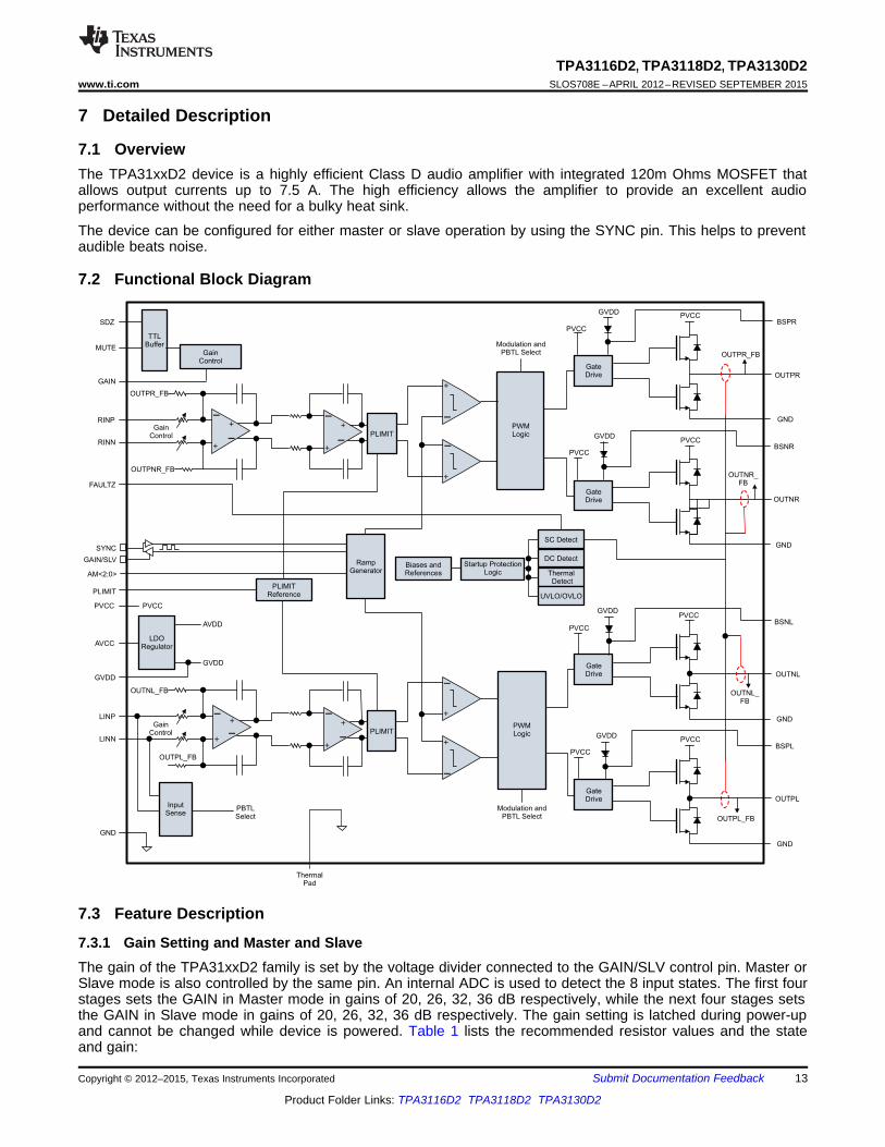
7 Detailed Description
7.1 OverviewThe TPA31xxD2 device is a highly efficient Class D audio amplifier with integrated 120m Ohms MOSFET thatallows output currents up to 7.5 A. The high efficiency allows the amplifier to provide an excellent audioperformance without the need for a bulky heat sink.
The device can be configured for either master or slave operation by using the SYNC pin. This helps to preventaudible beats noise.
7.2 Functional Block Diagram
7.3 Feature Description
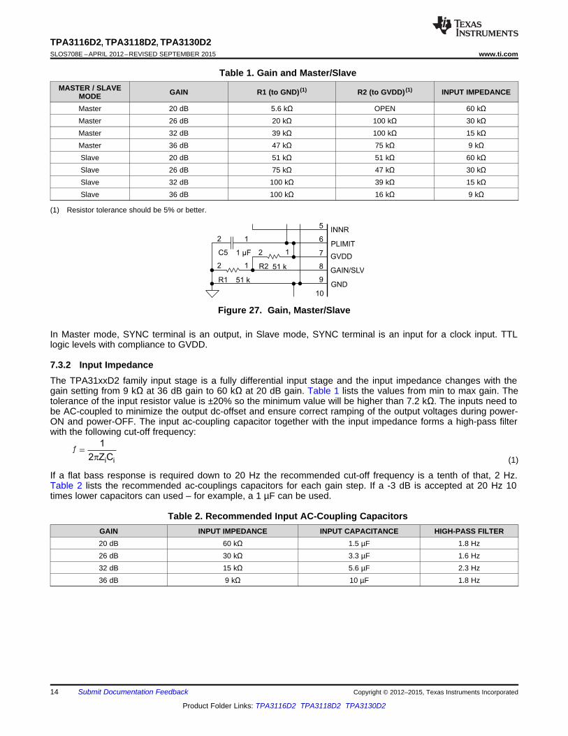
7.3.1 Gain Setting and Master and SlaveThe gain of the TPA31xxD2 family is set by the voltage divider connected to the GAIN/SLV control pin. Master orSlave mode is also controlled by the same pin. An internal ADC is used to detect the 8 input states. The first fourstages sets the GAIN in Master mode in gains of 20, 26, 32, 36 dB respectively, while the next four stages setsthe GAIN in Slave mode in gains of 20, 26, 32, 36 dB respectively. The gain setting is latched during power-upand cannot be changed while device is powered. Table 1 lists the recommended resistor values and the stateand gain:
Copyright © 2012–2015, Texas Instruments Incorporated Submit Documentation Feedback 13
Product Folder Links: TPA3116D2 TPA3118D2 TPA3130D2
i i
1f
2 Z Cp
=ƒ
5
6
7
8
9
10
INNR
PLIMIT
GVDD
GAIN/SLV
GND
2 1
12C5 1 Fµ
2 1
51 kR1
51 kR2
TPA3116D2, TPA3118D2, TPA3130D2SLOS708E –APRIL 2012–REVISED SEPTEMBER 2015 www.ti.com
Table 1. Gain and Master/SlaveMASTER / SLAVE GAIN R1 (to GND) (1) R2 (to GVDD) (1) INPUT IMPEDANCEMODE
Master 20 dB 5.6 kΩ OPEN 60 kΩMaster 26 dB 20 kΩ 100 kΩ 30 kΩMaster 32 dB 39 kΩ 100 kΩ 15 kΩMaster 36 dB 47 kΩ 75 kΩ 9 kΩSlave 20 dB 51 kΩ 51 kΩ 60 kΩSlave 26 dB 75 kΩ 47 kΩ 30 kΩSlave 32 dB 100 kΩ 39 kΩ 15 kΩSlave 36 dB 100 kΩ 16 kΩ 9 kΩ
(1) Resistor tolerance should be 5% or better.
Figure 27. Gain, Master/Slave
In Master mode, SYNC terminal is an output, in Slave mode, SYNC terminal is an input for a clock input. TTLlogic levels with compliance to GVDD.
7.3.2 Input ImpedanceThe TPA31xxD2 family input stage is a fully differential input stage and the input impedance changes with thegain setting from 9 kΩ at 36 dB gain to 60 kΩ at 20 dB gain. Table 1 lists the values from min to max gain. Thetolerance of the input resistor value is ±20% so the minimum value will be higher than 7.2 kΩ. The inputs need tobe AC-coupled to minimize the output dc-offset and ensure correct ramping of the output voltages during power-ON and power-OFF. The input ac-coupling capacitor together with the input impedance forms a high-pass filterwith the following cut-off frequency:
(1)
If a flat bass response is required down to 20 Hz the recommended cut-off frequency is a tenth of that, 2 Hz.Table 2 lists the recommended ac-couplings capacitors for each gain step. If a -3 dB is accepted at 20 Hz 10times lower capacitors can used – for example, a 1 µF can be used.
Table 2. Recommended Input AC-Coupling CapacitorsGAIN INPUT IMPEDANCE INPUT CAPACITANCE HIGH-PASS FILTER20 dB 60 kΩ 1.5 µF 1.8 Hz26 dB 30 kΩ 3.3 µF 1.6 Hz32 dB 15 kΩ 5.6 µF 2.3 Hz36 dB 9 kΩ 10 µF 1.8 Hz
14 Submit Documentation Feedback Copyright © 2012–2015, Texas Instruments Incorporated
Product Folder Links: TPA3116D2 TPA3118D2 TPA3130D2
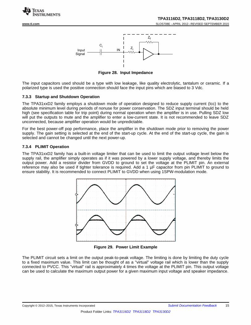
InputSignal
Ci
INZi
Zf
TPA3116D2, TPA3118D2, TPA3130D2www.ti.com SLOS708E –APRIL 2012–REVISED SEPTEMBER 2015
Figure 28. Input Impedance
The input capacitors used should be a type with low leakage, like quality electrolytic, tantalum or ceramic. If apolarized type is used the positive connection should face the input pins which are biased to 3 Vdc.
7.3.3 Startup and Shutdown OperationThe TPA31xxD2 family employs a shutdown mode of operation designed to reduce supply current (Icc) to theabsolute minimum level during periods of nonuse for power conservation. The SDZ input terminal should be heldhigh (see specification table for trip point) during normal operation when the amplifier is in use. Pulling SDZ lowwill put the outputs to mute and the amplifier to enter a low-current state. It is not recommended to leave SDZunconnected, because amplifier operation would be unpredictable.
For the best power-off pop performance, place the amplifier in the shutdown mode prior to removing the powersupply. The gain setting is selected at the end of the start-up cycle. At the end of the start-up cycle, the gain isselected and cannot be changed until the next power-up.
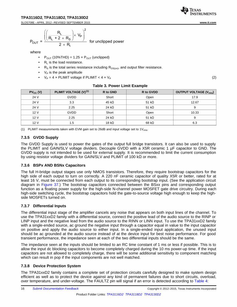
7.3.4 PLIMIT OperationThe TPA31xxD2 family has a built-in voltage limiter that can be used to limit the output voltage level below thesupply rail, the amplifier simply operates as if it was powered by a lower supply voltage, and thereby limits theoutput power. Add a resistor divider from GVDD to ground to set the voltage at the PLIMIT pin. An externalreference may also be used if tighter tolerance is required. Add a 1 µF capacitor from pin PLIMIT to ground toensure stability. It is recommended to connect PLIMIT to GVDD when using 1SPW-modulation mode.
Figure 29. Power Limit Example
The PLIMIT circuit sets a limit on the output peak-to-peak voltage. The limiting is done by limiting the duty cycleto a fixed maximum value. This limit can be thought of as a "virtual" voltage rail which is lower than the supplyconnected to PVCC. This "virtual" rail is approximately 4 times the voltage at the PLIMIT pin. This output voltagecan be used to calculate the maximum output power for a given maximum input voltage and speaker impedance.
Copyright © 2012–2015, Texas Instruments Incorporated Submit Documentation Feedback 15
Product Folder Links: TPA3116D2 TPA3118D2 TPA3130D2
2
LP
L SOUT
L
RV
R + 2 RP = for unclipped power
2 R
æ öæ ö´ç ÷ç ÷ç ÷´è øè ø
´
TPA3116D2, TPA3118D2, TPA3130D2SLOS708E –APRIL 2012–REVISED SEPTEMBER 2015 www.ti.com
where• POUT (10%THD) = 1.25 × POUT (unclipped)• RL is the load resistance.• RS is the total series resistance including RDS(on), and output filter resistance.• VP is the peak amplitude• VP = 4 × PLIMIT voltage if PLIMIT < 4 × VP (2)
Table 3. Power Limit ExamplePVCC (V) PLIMIT VOLTAGE (V) (1) R to GND R to GVDD OUTPUT VOLTAGE (Vrms)
24 V GVDD Short Open 17.924 V 3.3 45 kΩ 51 kΩ 12.6724 V 2.25 24 kΩ 51 kΩ 912 V GVDD Short Open 10.3312 V 2.25 24 kΩ 51 kΩ 912 V 1.5 18 kΩ 68 kΩ 6.3
(1) PLIMIT measurements taken with EVM gain set to 26dB and input voltage set to 1Vrms.
7.3.5 GVDD SupplyThe GVDD Supply is used to power the gates of the output full bridge transistors. It can also be used to supplythe PLIMIT and GAIN/SLV voltage dividers. Decouple GVDD with a X5R ceramic 1 µF capacitor to GND. TheGVDD supply is not intended to be used for external supply. It is recommended to limit the current consumptionby using resistor voltage dividers for GAIN/SLV and PLIMIT of 100 kΩ or more.
7.3.6 BSPx AND BSNx CapacitorsThe full H-bridge output stages use only NMOS transistors. Therefore, they require bootstrap capacitors for thehigh side of each output to turn on correctly. A 220 nF ceramic capacitor of quality X5R or better, rated for atleast 16 V, must be connected from each output to its corresponding bootstrap input. (See the application circuitdiagram in Figure 37.) The bootstrap capacitors connected between the BSxx pins and corresponding outputfunction as a floating power supply for the high-side N-channel power MOSFET gate drive circuitry. During eachhigh-side switching cycle, the bootstrap capacitors hold the gate-to-source voltage high enough to keep the high-side MOSFETs turned on.
7.3.7 Differential InputsThe differential input stage of the amplifier cancels any noise that appears on both input lines of the channel. Touse the TPA31xxD2 family with a differential source, connect the positive lead of the audio source to the RINP orLINP input and the negative lead from the audio source to the RINN or LINN input. To use the TPA31xxD2 familywith a single-ended source, ac ground the negative input through a capacitor equal in value to the input capacitoron positive and apply the audio source to either input. In a single-ended input application, the unused inputshould be ac grounded at the audio source instead of at the device input for best noise performance. For goodtransient performance, the impedance seen at each of the two differential inputs should be the same.
The impedance seen at the inputs should be limited to an RC time constant of 1 ms or less if possible. This is toallow the input dc blocking capacitors to become completely charged during the 10 ms power-up time. If the inputcapacitors are not allowed to completely charge, there will be some additional sensitivity to component matchingwhich can result in pop if the input components are not well matched.
7.3.8 Device Protection SystemThe TPA31xxD2 family contains a complete set of protection circuits carefully designed to make system designefficient as well as to protect the device against any kind of permanent failures due to short circuits, overload,over temperature, and under-voltage. The FAULTZ pin will signal if an error is detected according to Table 4:
16 Submit Documentation Feedback Copyright © 2012–2015, Texas Instruments Incorporated
Product Folder Links: TPA3116D2 TPA3118D2 TPA3130D2
TPA3116D2, TPA3118D2, TPA3130D2www.ti.com SLOS708E –APRIL 2012–REVISED SEPTEMBER 2015
Table 4. Fault ReportingTRIGGERING CONDITION LATCHED/SELF-FAULT FAULTZ ACTION(typical value) CLEARING
Over Current Output short or short to PVCC or GND Low Output high impedance LatchedOver Temperature Tj > 150°C Low Output high impedance Latched
Too High DC Offset DC output voltage Low Output high impedance LatchedUnder Voltage on PVCC < 4.5V – Output high impedance Self-clearingPVCCOver Voltage on PVCC > 27V – Output high impedance Self-clearingPVCC
7.3.9 DC Detect ProtectionThe TPA31xxD2 family has circuitry which will protect the speakers from DC current which might occur due todefective capacitors on the input or shorts on the printed circuit board at the inputs. A DC detect fault will bereported on the FAULT pin as a low state. The DC Detect fault will also cause the amplifier to shutdown bychanging the state of the outputs to Hi-Z.
If automatic recovery from the short circuit protection latch is desired, connect the FAULTZ pin directly to theSDZ pin. This allows the FAULTZ pin function to automatically drive the SDZ pin low which clears the DC Detectprotection latch.
A DC Detect Fault is issued when the output differential duty-cycle of either channel exceeds 60% for more than420 msec at the same polarity. Table x below shows some examples of the typical DC Detect Protectionthreshold for several values of the supply voltage. This feature protects the speaker from large DC currents orAC currents less than 2Hz. To avoid nuisance faults due to the DC detect circuit, hold the SD pin low at power-up until the signals at the inputs are stable. Also, take care to match the impedance seen at the positive andnegative inputs to avoid nuisance DC detect faults.
Table 5 lists the minimum output offset voltages required to trigger the DC detect. The outputs must remain at orabove the voltage listed in the table for more than 420 ms to trigger the DC detect.
Table 5. DC Detect ThresholdPVCC (V) VOS - OUTPUT OFFSET VOLTAGE (V)
4.5 0.966 1.312 2.618 3.9
7.3.10 Short-Circuit Protection and Automatic Recovery FeatureThe TPA31xxD2 family has protection from over current conditions caused by a short circuit on the output stage.The short circuit protection fault is reported on the FAULTZ pin as a low state. The amplifier outputs are switchedto a high impedance state when the short circuit protection latch is engaged. The latch can be cleared by cyclingthe SDZ pin through the low state.
If automatic recovery from the short circuit protection latch is desired, connect the FAULTZ pin directly to theSDZ pin. This allows the FAULTZ pin function to automatically drive the SDZ pin low which clears the short-circuit protection latch.
In systems where a possibility of a permanent short from the output to PVDD or to a high voltage battery like acar battery can occur, pull the MUTE pin low with the FAULTZ signal with a inverting transistor to ensure a high-Z restart, like shown in the figure below:
Copyright © 2012–2015, Texas Instruments Incorporated Submit Documentation Feedback 17
Product Folder Links: TPA3116D2 TPA3118D2 TPA3130D2

> 1.4sec
mP TPA3116D2
SDZ
MUTE
FAULTZ
SDZ
MUTE
FAULTZ
TPA3116D2, TPA3118D2, TPA3130D2SLOS708E –APRIL 2012–REVISED SEPTEMBER 2015 www.ti.com
Figure 30. MUTE Driven by Inverted FAULTZ Figure 31. Timing Requirement for SDZ
7.3.11 Thermal ProtectionThermal protection on the TPA31xxD2 family prevents damage to the device when the internal die temperatureexceeds 150°C. There is a ±15°C tolerance on this trip point from device to device. Once the die temperatureexceeds the thermal trip point, the device enters into the shutdown state and the outputs are disabled. This is alatched fault.
Thermal protection faults are reported on the FAULTZ terminal as a low state.
If automatic recovery from the thermal protection latch is desired, connect the FAULTZ pin directly to the SDZpin. This allows the FAULTZ pin function to automatically drive the SDZ pin low which clears the thermalprotection latch.
7.3.12 Device Modulation SchemeThe TPA31xxD2 family has the option of running in either BD modulation or 1SPW modulation; this is set by theMODSEL pin.
7.3.12.1 MODSEL = GND: BD-ModulationThis is a modulation scheme that allows operation without the classic LC reconstruction filter when the amp isdriving an inductive load with short speaker wires. Each output is switching from 0 volts to the supply voltage.The OUTPx and OUTNx are in phase with each other with no input so that there is little or no current in thespeaker. The duty cycle of OUTPx is greater than 50% and OUTNx is less than 50% for positive output voltages.The duty cycle of OUTPx is less than 50% and OUTNx is greater than 50% for negative output voltages. Thevoltage across the load sits at 0V throughout most of the switching period, reducing the switching current, whichreduces any I2R losses in the load.
18 Submit Documentation Feedback Copyright © 2012–2015, Texas Instruments Incorporated
Product Folder Links: TPA3116D2 TPA3118D2 TPA3130D2

OUTP
OUTN
OUTP-OUTN
Speaker
Current
OUTP
OUTN
OUTP-OUTN
Speaker
Current
OUTP
OUTN
OUTP-OUTN
Speaker
Current
0V
0V
PVCC
No Output
Positive Output
Negative Output
0A
0A
0V
-PVCC
TPA3116D2, TPA3118D2, TPA3130D2www.ti.com SLOS708E –APRIL 2012–REVISED SEPTEMBER 2015
Figure 32. BD Mode Modulation
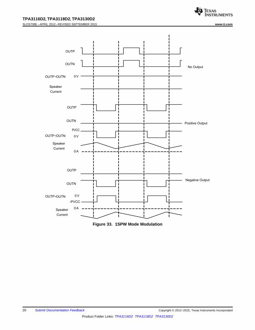
7.3.12.2 MODSEL = HIGH: 1SPW-modulationThe 1SPW mode alters the normal modulation scheme in order to achieve higher efficiency with a slight penaltyin THD degradation and more attention required in the output filter selection. In 1SPW mode the outputs operateat ~15% modulation during idle conditions. When an audio signal is applied one output will decrease and one willincrease. The decreasing output signal will quickly rail to GND at which point all the audio modulation takes placethrough the rising output. The result is that only one output is switching during a majority of the audio cycle.Efficiency is improved in this mode due to the reduction of switching losses. The THD penalty in 1SPW mode isminimized by the high performance feedback loop. The resulting audio signal at each half output has adiscontinuity each time the output rails to GND. This can cause ringing in the audio reconstruction filter unlesscare is taken in the selection of the filter components and type of filter used.
Copyright © 2012–2015, Texas Instruments Incorporated Submit Documentation Feedback 19
Product Folder Links: TPA3116D2 TPA3118D2 TPA3130D2
OUTP
OUTN
OUTP-OUTN
Speaker
Current
OUTP
OUTN
OUTP-OUTN
Speaker
Current
OUTP
OUTN
OUTP-OUTN
Speaker
Current
0 V
0 V
PVCC
No Output
Positive Output
Negative Output
0 A
0 A
0 V
-PVCC
TPA3116D2, TPA3118D2, TPA3130D2SLOS708E –APRIL 2012–REVISED SEPTEMBER 2015 www.ti.com
Figure 33. 1SPW Mode Modulation
20 Submit Documentation Feedback Copyright © 2012–2015, Texas Instruments Incorporated
Product Folder Links: TPA3116D2 TPA3118D2 TPA3130D2
TPA3116D2, TPA3118D2, TPA3130D2www.ti.com SLOS708E –APRIL 2012–REVISED SEPTEMBER 2015
7.3.13 Efficiency: LC Filter Required with the Traditional Class-D Modulation SchemeThe main reason that the traditional class-D amplifier-based on AD modulation needs an output filter is that theswitching waveform results in maximum current flow. This causes more loss in the load, which causes lowerefficiency. The ripple current is large for the traditional modulation scheme, because the ripple current isproportional to voltage multiplied by the time at that voltage. The differential voltage swing is 2 × VCC, and thetime at each voltage is half the period for the traditional modulation scheme. An ideal LC filter is needed to storethe ripple current from each half cycle for the next half cycle, while any resistance causes power dissipation. Thespeaker is both resistive and reactive, whereas an LC filter is almost purely reactive.
The TPA3116D2 modulation scheme has little loss in the load without a filter because the pulses are short andthe change in voltage is VCC instead of 2 × VCC. As the output power increases, the pulses widen, making theripple current larger. Ripple current could be filtered with an LC filter for increased efficiency, but for mostapplications the filter is not needed.
An LC filter with a cutoff frequency less than the class-D switching frequency allows the switching current to flowthrough the filter instead of the load. The filter has less resistance but higher impedance at the switchingfrequency than the speaker, which results in less power dissipation, therefore increasing efficiency.
7.3.14 Ferrite Bead Filter ConsiderationsUsing the Advanced Emissions Suppression Technology in the TPA3116D2 amplifier it is possible to design ahigh efficiency class-D audio amplifier while minimizing interference to surrounding circuits. It is also possible toaccomplish this with only a low-cost ferrite bead filter. In this case it is necessary to carefully select the ferritebead used in the filter. One important aspect of the ferrite bead selection is the type of material used in the ferritebead. Not all ferrite material is alike, so it is important to select a material that is effective in the 10 to 100 MHzrange which is key to the operation of the class-D amplifier. Many of the specifications regulating consumerelectronics have emissions limits as low as 30 MHz. It is important to use the ferrite bead filter to block radiationin the 30 MHz and above range from appearing on the speaker wires and the power supply lines which are goodantennas for these signals. The impedance of the ferrite bead can be used along with a small capacitor with avalue in the range of 1000 pF to reduce the frequency spectrum of the signal to an acceptable level. For bestperformance, the resonant frequency of the ferrite bead/ capacitor filter should be less than 10 MHz.
Also, it is important that the ferrite bead is large enough to maintain its impedance at the peak currents expectedfor the amplifier. Some ferrite bead manufacturers specify the bead impedance at a variety of current levels. Inthis case it is possible to make sure the ferrite bead maintains an adequate amount of impedance at the peakcurrent the amplifier will see. If these specifications are not available, it is also possible to estimate the beadcurrent handling capability by measuring the resonant frequency of the filter output at low power and at maximumpower. A change of resonant frequency of less than fifty percent under this condition is desirable. Examples offerrite beads which have been tested and work well with the TPA3130D2 can be seen in the TPA3130D2EVMuser guide SLOU341.
A high quality ceramic capacitor is also needed for the ferrite bead filter. A low ESR capacitor with goodtemperature and voltage characteristics will work best.
Additional EMC improvements may be obtained by adding snubber networks from each of the class-D outputs toground. Suggested values for a simple RC series snubber network would be 18 Ω in series with a 330 pFcapacitor although design of the snubber network is specific to every application and must be designed takinginto account the parasitic reactance of the printed circuit board as well as the audio amp. Take care to evaluatethe stress on the component in the snubber network especially if the amp is running at high PVCC. Also, makesure the layout of the snubber network is tight and returns directly to the GND pins on the IC.
Copyright © 2012–2015, Texas Instruments Incorporated Submit Documentation Feedback 21
Product Folder Links: TPA3116D2 TPA3118D2 TPA3130D2
TPA3116D2, TPA3118D2, TPA3130D2SLOS708E –APRIL 2012–REVISED SEPTEMBER 2015 www.ti.com
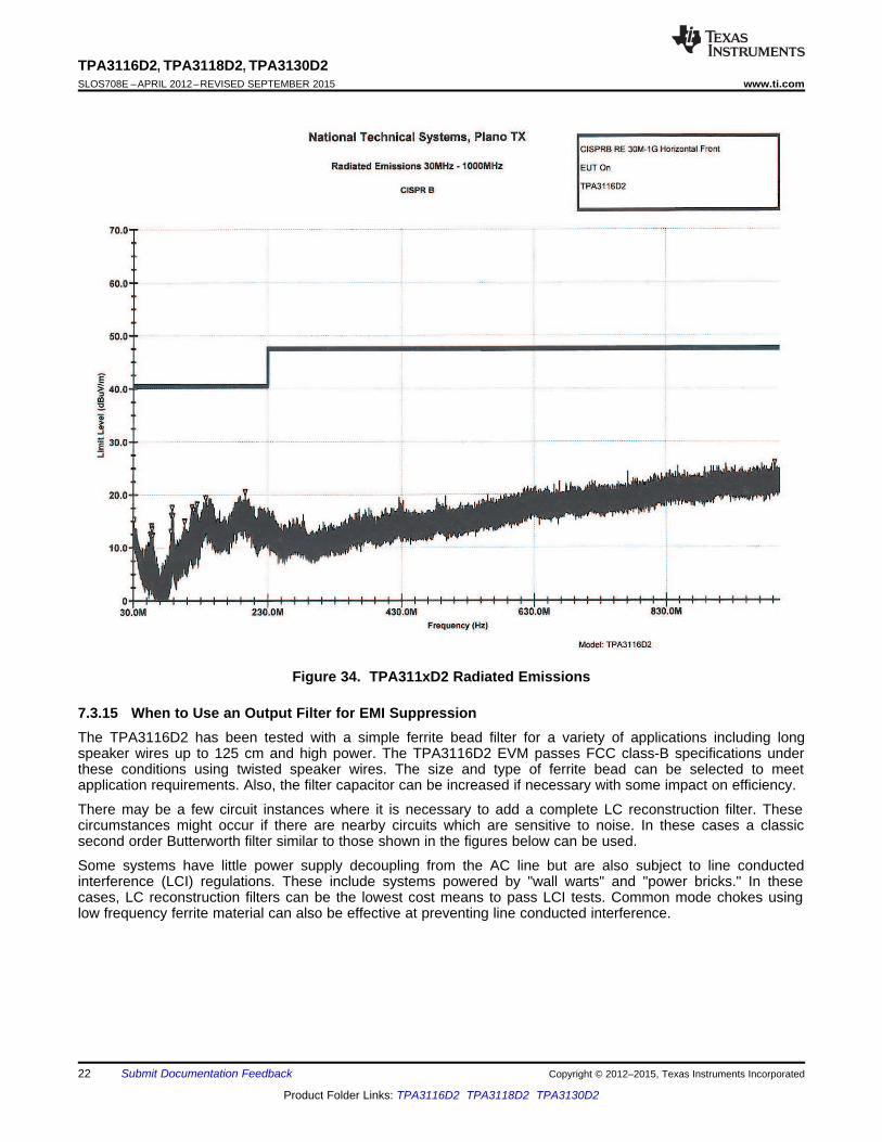
Figure 34. TPA311xD2 Radiated Emissions
7.3.15 When to Use an Output Filter for EMI SuppressionThe TPA3116D2 has been tested with a simple ferrite bead filter for a variety of applications including longspeaker wires up to 125 cm and high power. The TPA3116D2 EVM passes FCC class-B specifications underthese conditions using twisted speaker wires. The size and type of ferrite bead can be selected to meetapplication requirements. Also, the filter capacitor can be increased if necessary with some impact on efficiency.
There may be a few circuit instances where it is necessary to add a complete LC reconstruction filter. Thesecircumstances might occur if there are nearby circuits which are sensitive to noise. In these cases a classicsecond order Butterworth filter similar to those shown in the figures below can be used.
Some systems have little power supply decoupling from the AC line but are also subject to line conductedinterference (LCI) regulations. These include systems powered by "wall warts" and "power bricks." In thesecases, LC reconstruction filters can be the lowest cost means to pass LCI tests. Common mode chokes usinglow frequency ferrite material can also be effective at preventing line conducted interference.
22 Submit Documentation Feedback Copyright © 2012–2015, Texas Instruments Incorporated
Product Folder Links: TPA3116D2 TPA3118D2 TPA3130D2
OUTP
OUTN
10 µH
L1
10 µH
L2
C2
C3
0.68 µF
0.68 µF
OUTP
OUTN
FerriteChip Bead
1 nF
1 nF
FerriteChip Bead
4 - 8W W
4 - 8W W
TPA3116D2, TPA3118D2, TPA3130D2www.ti.com SLOS708E –APRIL 2012–REVISED SEPTEMBER 2015
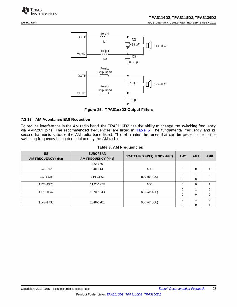
Figure 35. TPA31xxD2 Output Filters
7.3.16 AM Avoidance EMI ReductionTo reduce interference in the AM radio band, the TPA3116D2 has the ability to change the switching frequencyvia AM<2:0> pins. The recommended frequencies are listed in Table 6. The fundamental frequency and itssecond harmonic straddle the AM radio band listed. This eliminates the tones that can be present due to theswitching frequency being demodulated by the AM radio.
Table 6. AM FrequenciesUS EUROPEAN
SWITCHING FREQUENCY (kHz) AM2 AM1 AM0AM FREQUENCY (kHz) AM FREQUENCY (kHz)
522-540540-917 540-914 500 0 0 1
0 1 0917-1125 914-1122 600 (or 400)
0 0 01125-1375 1122-1373 500 0 0 1
0 1 01375-1547 1373-1548 600 (or 400)
0 0 00 1 0
1547-1700 1548-1701 600 (or 500)0 0 1
Copyright © 2012–2015, Texas Instruments Incorporated Submit Documentation Feedback 23
Product Folder Links: TPA3116D2 TPA3118D2 TPA3130D2
TPA3116D2 4.5 V–26 VPSU
LC Filter
OUTPR
OUTNR
OUTPL
OUTNL
Right
Left PBTLDetect
TPA3116D2, TPA3118D2, TPA3130D2SLOS708E –APRIL 2012–REVISED SEPTEMBER 2015 www.ti.com
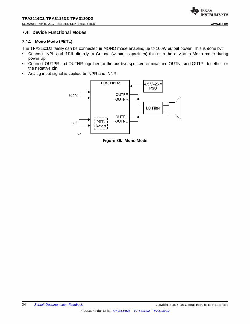
7.4 Device Functional Modes
7.4.1 Mono Mode (PBTL)The TPA31xxD2 family can be connected in MONO mode enabling up to 100W output power. This is done by:• Connect INPL and INNL directly to Ground (without capacitors) this sets the device in Mono mode during
power up.• Connect OUTPR and OUTNR together for the positive speaker terminal and OUTNL and OUTPL together for
the negative pin.• Analog input signal is applied to INPR and INNR.
Figure 36. Mono Mode
24 Submit Documentation Feedback Copyright © 2012–2015, Texas Instruments Incorporated
Product Folder Links: TPA3116D2 TPA3118D2 TPA3130D2

TPA3116D2, TPA3118D2, TPA3130D2www.ti.com SLOS708E –APRIL 2012–REVISED SEPTEMBER 2015
8 Applications and Implementation
NOTEInformation in the following applications sections is not part of the TI componentspecification, and TI does not warrant its accuracy or completeness. TI’s customers areresponsible for determining suitability of components for their purposes. Customers shouldvalidate and test their design implementation to confirm system functionality.
8.1 Application InformationThis section describes a 2.1 Master and Slave application. The Master is configured as stereo outputs and theSlave is configured as mono PBTL output.
8.2 Typical ApplicationA 2.1 solution, U1 TPA3116D2 in Master mode 400 kHz, BTL, gain if 20 dB, power limit not implemented. U2 inSlave, PBTL mode gain of 20dB. Inputs are connected for differential inputs.
Copyright © 2012–2015, Texas Instruments Incorporated Submit Documentation Feedback 25
Product Folder Links: TPA3116D2 TPA3118D2 TPA3130D2

PowerPad
U1
TPA3116D2
MODSEL1
SDZ2
FAULTZ3
INPR4
INNR5
PLIMIT6
GVDD7
GAIN/SLV8
GND9
INPL10
INNL11
MUTE12
AM213
AM114
AM015
SYNC16
PVCC32
PVCC31
BSPR30
OUTPR29
GND28
OUTNR27
BSNR26
GND25
BSPL24
OUTPL23
GND22
OUTNL21
BSNL20
PVCC19
PVCC18
AVCC17
PVCC DECOUPLING
C17 220nF
21
PVCC DECOUPLING
GN
D
C16 220nF21
C13 1uF2 1
C58 100nF
21
C29680nF
21
L7 10uH
1 2
R10 3.3R
1 2
L8 10uH
1 2
C28680nF
21
L910uH
1 2
C5710nF
21
R12
20k
12 L10 10uH
1 2
C3810nF
21
R14 100k
1 2
C25
220uF
12
C26680nF
21
R183.3R
12
C4010nF
21
R173.3R
12
GN
D
C41
1nF
21
C321nF
21
C11 1uF2 1
C22
220uF
12
GND
C21
100nF
21
C201nF
21
C311nF
21
R153.3R
12
C331nF
21
R163.3R
12
GN
D
C19 220nF
21
C301nF
21
C27680nF
21
C3410nF
21
C3710nF
21
IN_P_LEFT
IN_N_RIGHT
IN_N_LEFT
IN_P_RIGHT
GND
PVCC
GND GND
GND
GND
GND
GND GND
GND
OU
T_
N_LE
FT
OU
T_P
_L
EF
T
-
+
OU
T_N
_R
IGH
TO
UT
_P
_R
IGH
T
+
-PVCC
C14 1uF
2 1
R11
100k
12
MUTE_LR
OUTPUT LC FILTER
R13
100k
12
C15
1uF
21
EMI C-RC SNUBBER
C24
100nF
21
GND
PVCC
C18 220nF21
GND
/SD_LR
PVCC
C23
1nF
21
GND
C12 1uF
2 1
R73
10k
12
C42 220nF21
L15 10uH
1 2
L16 10uH
1 2
R21
75k
12
R22
100k
12
C50
220uF
12
C511uF
21
GN
D
C35 1uF2 1
GND
C47
220uF
12
C46
100nF
21
C451nF
21
C541nF
21
R233.3R
12
GN
D
R243.3R
12
C44 220nF
21
C531nF
21
C521uF
21
C5510nF
21
C5610nF
21
IN_P_SUB
IN_N_SUB
GND
SY
NC
GND
GND
GND
-
+
OU
T_P
_S
UB
OU
T_N
_S
UB
PVCC
MUTE_SUB
R20
47k
12
OUTPUT LC FILTER
R19
100k
12
C39
1uF
21
C49
100nF
21
EMI C-RC SNUBBER
PVCC
C43 220nF21
PVCC
/SD_SUB
C48
1nF
21
GND
C36 1uF
2 1
GND
PowerPad
U2
TPA3116D2
MODSEL1
SDZ2
FAULTZ3
INPR4
INNR5
PLIMIT6
GVDD7
GAIN/SLV8
GND9
INPL10
INNL11
MUTE12
AM213
AM114
AM015
SYNC16
PVCC32
PVCC31
BSPR30
OUTPR29
GND28
OUTNR27
BSNR26
GND25
BSPL24
OUTPL23
GND22
OUTNL21
BSNL20
PVCC19
PVCC18
AVCC17
PVCC DECOUPLING
C43 220nF
21
PVCC DECOUPLING
GN
D
4R
4R
2R
TPA3116D2, TPA3118D2, TPA3130D2SLOS708E –APRIL 2012–REVISED SEPTEMBER 2015 www.ti.com
Typical Application (continued)
Figure 37. Schematic
8.2.1 Design Requriements
DESIGN PARAMETERS EXAMPLE VALUEInput voltage range PVCC 4.5 V to 26 VPWM output frequencies 400 kHz, 500 kHz, 600 kHz, 1 MHz or 1.2 MHzMaximum output power 50 W
26 Submit Documentation Feedback Copyright © 2012–2015, Texas Instruments Incorporated
Product Folder Links: TPA3116D2 TPA3118D2 TPA3130D2

TPA3116D2, TPA3118D2, TPA3130D2www.ti.com SLOS708E –APRIL 2012–REVISED SEPTEMBER 2015
8.2.2 Detailed Design ProcedureThe TPA31xxD2 family is a very flexible and easy to use Class D amplifier; therefore the design process isstraightforward. Before beginning the design, gather the following information regarding the audio system.• PVCC rail planned for the design• Speaker or load impedance• Maximum output power requirement• Desired PWM frequency
8.2.2.1 Select the PWM FrequencySet the PWM frequency by using AM0, AM1 and AM2 pins.
8.2.2.2 Select the Amplifier Gain and Master/Slave ModeIn order to select the amplifier gain setting, the designer must determine the maximum power target and thespeaker impedance. Once these parameters have been determined, calculate the required output voltage swingwhich delivers the maximum output power.
Choose the lowest analog gain setting that corresponds to produce an output voltage swing greater than therequired output swing for maximum power. The analog gain and master/slave mode can be set by selecting thevoltage divider resistors (R1 and R2) on the Gain/SLV pin.
8.2.2.3 Select Input CapacitanceSelect the bulk capacitors at the PVCC inputs for proper voltage margin and adequate capacitance to support thepower requirements. In practice, with a well-designed power supply, two 100-μF, 50-V capacitors should besufficient. One capacitor should be placed near the PVCC inputs at each side of the device. PVCC capacitorsshould be a low ESR type because they are being used in a high-speed switching application.
8.2.2.4 Select Decoupling CapacitorsGood quality decoupling capacitors need to be added at each of the PVCC inputs to provide good reliability,good audio performance, and to meet regulatory requirements. X5R or better ratings should be used in thisapplication. Consider temperature, ripple current, and voltage overshoots when selecting decoupling capacitors.Also, these decoupling capacitors should be located near the PVCC and GND connections to the device in orderto minimize series inductances.
8.2.2.5 Select Bootstrap CapacitorsEach of the outputs require bootstrap capacitors to provide gate drive for the high-side output FETs. For thisdesign, use 0.22-μF, 25-V capacitors of X5R quality or better.
Copyright © 2012–2015, Texas Instruments Incorporated Submit Documentation Feedback 27
Product Folder Links: TPA3116D2 TPA3118D2 TPA3130D2
0.001
0.01
0.1
1
10
0.01 0.1 1 10 40Output Power (W)
TH
D+
N (
%)
f = 20Hzf = 1kHzf = 6kHz
Gain = 26dBPVCC = 12VTA = 25°CRL = 4Ω
G009
0.001
0.01
0.1
1
10
0.01 0.1 1 10 100Output Power (W)
TH
D+
N (
%)
f = 20Hzf = 1kHzf = 6kHz
Gain = 26dBPVCC = 24VTA = 25°CRL = 4Ω
G010
TPA3116D2, TPA3118D2, TPA3130D2SLOS708E –APRIL 2012–REVISED SEPTEMBER 2015 www.ti.com
8.2.3 Application Curves
Figure 38. Total Harmonic Distortion + Noise (BTL) vs Figure 39. Total Harmonic Distortion + Noise (BTL) vsOutput Power Output Power
9 Power Supply Recommendations
The power supply requirements for the TPA3116D2 consist of one higher-voltage supply to power the outputstage of the speaker amplifier. Several on-chip regulators are included on the TPA3116D2 to generate thevoltages necessary for the internal circuitry of the audio path. It is important to note that the voltage regulatorswhich have been integrated are sized only to provide the current necessary to power the internal circuitry. Theexternal pins are provided only as a connection point for off-chip bypass capacitors to filter the supply.Connecting external circuitry to these regulator outputs may result in reduced performance and damage to thedevice. The high voltage supply, between 4.5 V and 26 V, supplies the analog circuitry (AVCC) and the powerstage (PVCC). The AVCC supply feeds internal LDO including GVDD. This LDO output are connected toexternal pins for filtering purposes, but should not be connected to external circuits. GVDD LDO output havebeen sized to provide current necessary for internal functions but not for external loading.
10 Layout
10.1 Layout GuidelinesThe TPA3116D2 can be used with a small, inexpensive ferrite bead output filter for most applications. However,since the class-D switching edges are fast, it is necessary to take care when planning the layout of the printedcircuit board. The following suggestions will help to meet EMC requirements.• Decoupling capacitors — The high-frequency decoupling capacitors should be placed as close to the PVCC
and AVCC terminals as possible. Large (100 μF or greater) bulk power supply decoupling capacitors shouldbe placed near the TPA3116D2 on the PVCC supplies. Local, high-frequency bypass capacitors should beplaced as close to the PVCC pins as possible. These caps can be connected to the IC GND pad directly foran excellent ground connection. Consider adding a small, good quality low ESR ceramic capacitor between220 pF and 1 nF and a larger mid-frequency cap of value between 100 nF and 1 µF also of good quality tothe PVCC connections at each end of the chip.
• Keep the current loop from each of the outputs through the ferrite bead and the small filter cap and back toGND as small and tight as possible. The size of this current loop determines its effectiveness as an antenna.
• Grounding — The PVCC decoupling capacitors should connect to GND. All ground should be connected atthe IC GND, which should be used as a central ground connection or star ground for the TPA3116D2.
• Output filter — The ferrite EMI filter (see Figure 35) should be placed as close to the output terminals aspossible for the best EMI performance. The LC filter should be placed close to the outputs. The capacitorsused in both the ferrite and LC filters should be grounded.
28 Submit Documentation Feedback Copyright © 2012–2015, Texas Instruments Incorporated
Product Folder Links: TPA3116D2 TPA3118D2 TPA3130D2
TPA3116D2, TPA3118D2, TPA3130D2www.ti.com SLOS708E –APRIL 2012–REVISED SEPTEMBER 2015
Layout Guidelines (continued)For an example layout, see the TPA3116D2 Evaluation Module (TPA3116D2EVM) User Guide (SLOU336). Boththe EVM user manual and the thermal pad application reports, SLMA002 and SLMA004, are available on the TIWeb site at http://www.ti.com.
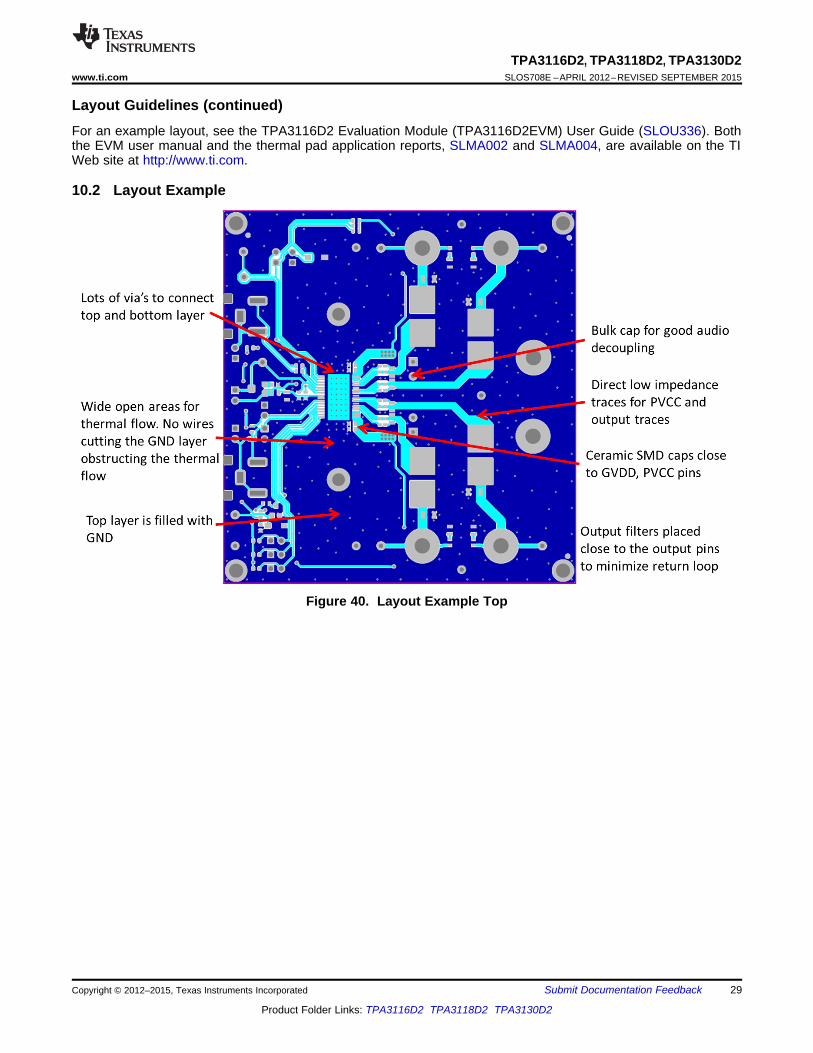
10.2 Layout Example
Figure 40. Layout Example Top
Copyright © 2012–2015, Texas Instruments Incorporated Submit Documentation Feedback 29
Product Folder Links: TPA3116D2 TPA3118D2 TPA3130D2
TPA3116D2, TPA3118D2, TPA3130D2SLOS708E –APRIL 2012–REVISED SEPTEMBER 2015 www.ti.com
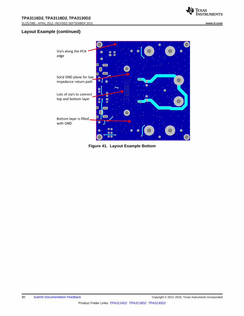
Layout Example (continued)
Figure 41. Layout Example Bottom
30 Submit Documentation Feedback Copyright © 2012–2015, Texas Instruments Incorporated
Product Folder Links: TPA3116D2 TPA3118D2 TPA3130D2
MACHINE THESE3 EDGES AFTERANODIZATION0.00
–0.60
+.000–.024
SINK HEIGHT
25.00
.984
1.00[.118]
3.00[.118]
0[.000]
10.0
0[.394]
19.5
0[.768]
30.5
0[1
.201]
40.0
0[1
.575]
50.00±0.38[1.969±.015]
SINK LENGTH
3.00[.118]
6.35[.250]
13.90±0.38[.547±.015]BASE WIDTH
6.95[.274]
5.00[.197]
40.00[1.575] 2X 4-40 6.5x
TPA3116D2, TPA3118D2, TPA3130D2www.ti.com SLOS708E –APRIL 2012–REVISED SEPTEMBER 2015
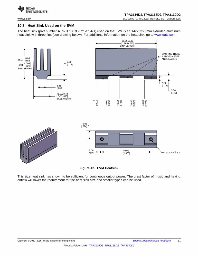
10.3 Heat Sink Used on the EVMThe heat sink (part number ATS-TI 10 OP-521-C1-R1) used on the EVM is an 14x25x50 mm extruded aluminumheat sink with three fins (see drawing below). For additional information on the heat sink, go to www.qats.com.
Figure 42. EVM Heatsink
This size heat sink has shown to be sufficient for continuous output power. The crest factor of music and havingairflow will lower the requirement for the heat sink size and smaller types can be used.
Copyright © 2012–2015, Texas Instruments Incorporated Submit Documentation Feedback 31
Product Folder Links: TPA3116D2 TPA3118D2 TPA3130D2
TPA3116D2, TPA3118D2, TPA3130D2SLOS708E –APRIL 2012–REVISED SEPTEMBER 2015 www.ti.com
11 Device and Documentation Support
11.1 Related LinksThe table below lists quick access links. Categories include technical documents, support and communityresources, tools and software, and quick access to sample or buy.
Table 7. Related LinksTECHNICAL TOOLS & SUPPORT &PARTS PRODUCT FOLDER SAMPLE & BUY DOCUMENTS SOFTWARE COMMUNITY
TPA3116D2 Click here Click here Click here Click here Click hereTPA3118D2 Click here Click here Click here Click here Click hereTPA3130D2 Click here Click here Click here Click here Click here
11.2 TrademarksAll trademarks are the property of their respective owners.
11.3 Electrostatic Discharge CautionThis integrated circuit can be damaged by ESD. Texas Instruments recommends that all integrated circuits be handled withappropriate precautions. Failure to observe proper handling and installation procedures can cause damage.
ESD damage can range from subtle performance degradation to complete device failure. Precision integrated circuits may be moresusceptible to damage because very small parametric changes could cause the device not to meet its published specifications.
11.4 GlossarySLYZ022 — TI Glossary.
This glossary lists and explains terms, acronyms, and definitions.
12 Mechanical, Packaging, and Orderable InformationThe following pages include mechanical, packaging, and orderable information. This information is the mostcurrent data available for the designated devices. This data is subject to change without notice and revision ofthis document. For browser-based versions of this data sheet, refer to the left-hand navigation.
32 Submit Documentation Feedback Copyright © 2012–2015, Texas Instruments Incorporated
Product Folder Links: TPA3116D2 TPA3118D2 TPA3130D2
PACKAGE OPTION ADDENDUM
www.ti.com 22-Sep-2015
Addendum-Page 1
PACKAGING INFORMATION
Orderable Device Status(1)
Package Type PackageDrawing
Pins PackageQty
Eco Plan(2)
Lead/Ball Finish(6)
MSL Peak Temp(3)
Op Temp (°C) Device Marking(4/5)
Samples
TPA3116D2DAD ACTIVE HTSSOP DAD 32 46 Green (RoHS& no Sb/Br)
CU NIPDAU Level-3-260C-168 HR -40 to 85 TPA3116D2
TPA3116D2DADR ACTIVE HTSSOP DAD 32 2000 Green (RoHS& no Sb/Br)
CU NIPDAU Level-3-260C-168 HR -40 to 85 TPA3116D2
TPA3118D2DAP ACTIVE HTSSOP DAP 32 46 Green (RoHS& no Sb/Br)
CU NIPDAU Level-3-260C-168 HR -40 to 85 TPA3118
TPA3118D2DAPR ACTIVE HTSSOP DAP 32 2000 Green (RoHS& no Sb/Br)
CU NIPDAU Level-3-260C-168 HR -40 to 85 TPA3118
TPA3130D2DAP ACTIVE HTSSOP DAP 32 46 Green (RoHS& no Sb/Br)
CU NIPDAU Level-3-260C-168 HR -40 to 85 TPA3130
TPA3130D2DAPR ACTIVE HTSSOP DAP 32 2000 Green (RoHS& no Sb/Br)
CU NIPDAU Level-3-260C-168 HR -40 to 85 TPA3130
(1) The marketing status values are defined as follows:ACTIVE: Product device recommended for new designs.LIFEBUY: TI has announced that the device will be discontinued, and a lifetime-buy period is in effect.NRND: Not recommended for new designs. Device is in production to support existing customers, but TI does not recommend using this part in a new design.PREVIEW: Device has been announced but is not in production. Samples may or may not be available.OBSOLETE: TI has discontinued the production of the device.
(2) Eco Plan - The planned eco-friendly classification: Pb-Free (RoHS), Pb-Free (RoHS Exempt), or Green (RoHS & no Sb/Br) - please check http://www.ti.com/productcontent for the latest availabilityinformation and additional product content details.TBD: The Pb-Free/Green conversion plan has not been defined.Pb-Free (RoHS): TI's terms "Lead-Free" or "Pb-Free" mean semiconductor products that are compatible with the current RoHS requirements for all 6 substances, including the requirement thatlead not exceed 0.1% by weight in homogeneous materials. Where designed to be soldered at high temperatures, TI Pb-Free products are suitable for use in specified lead-free processes.Pb-Free (RoHS Exempt): This component has a RoHS exemption for either 1) lead-based flip-chip solder bumps used between the die and package, or 2) lead-based die adhesive used betweenthe die and leadframe. The component is otherwise considered Pb-Free (RoHS compatible) as defined above.Green (RoHS & no Sb/Br): TI defines "Green" to mean Pb-Free (RoHS compatible), and free of Bromine (Br) and Antimony (Sb) based flame retardants (Br or Sb do not exceed 0.1% by weightin homogeneous material)
(3) MSL, Peak Temp. - The Moisture Sensitivity Level rating according to the JEDEC industry standard classifications, and peak solder temperature.
(4) There may be additional marking, which relates to the logo, the lot trace code information, or the environmental category on the device.
PACKAGE OPTION ADDENDUM
www.ti.com 22-Sep-2015
Addendum-Page 2
(5) Multiple Device Markings will be inside parentheses. Only one Device Marking contained in parentheses and separated by a "~" will appear on a device. If a line is indented then it is a continuationof the previous line and the two combined represent the entire Device Marking for that device.
(6) Lead/Ball Finish - Orderable Devices may have multiple material finish options. Finish options are separated by a vertical ruled line. Lead/Ball Finish values may wrap to two lines if the finishvalue exceeds the maximum column width.
Important Information and Disclaimer:The information provided on this page represents TI's knowledge and belief as of the date that it is provided. TI bases its knowledge and belief on informationprovided by third parties, and makes no representation or warranty as to the accuracy of such information. Efforts are underway to better integrate information from third parties. TI has taken andcontinues to take reasonable steps to provide representative and accurate information but may not have conducted destructive testing or chemical analysis on incoming materials and chemicals.TI and TI suppliers consider certain information to be proprietary, and thus CAS numbers and other limited information may not be available for release.
In no event shall TI's liability arising out of such information exceed the total purchase price of the TI part(s) at issue in this document sold by TI to Customer on an annual basis.
OTHER QUALIFIED VERSIONS OF TPA3116D2, TPA3118D2 :
• Automotive: TPA3116D2-Q1, TPA3118D2-Q1
NOTE: Qualified Version Definitions:
• Automotive - Q100 devices qualified for high-reliability automotive applications targeting zero defects
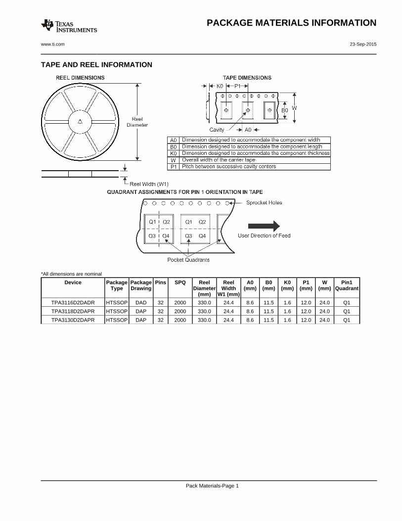
TAPE AND REEL INFORMATION
*All dimensions are nominal
Device PackageType
PackageDrawing
Pins SPQ ReelDiameter
(mm)
ReelWidth
W1 (mm)
A0(mm)
B0(mm)
K0(mm)
P1(mm)
W(mm)
Pin1Quadrant
TPA3116D2DADR HTSSOP DAD 32 2000 330.0 24.4 8.6 11.5 1.6 12.0 24.0 Q1
TPA3118D2DAPR HTSSOP DAP 32 2000 330.0 24.4 8.6 11.5 1.6 12.0 24.0 Q1
TPA3130D2DAPR HTSSOP DAP 32 2000 330.0 24.4 8.6 11.5 1.6 12.0 24.0 Q1
PACKAGE MATERIALS INFORMATION
www.ti.com 23-Sep-2015
Pack Materials-Page 1

*All dimensions are nominal
Device Package Type Package Drawing Pins SPQ Length (mm) Width (mm) Height (mm)
TPA3116D2DADR HTSSOP DAD 32 2000 367.0 367.0 45.0
TPA3118D2DAPR HTSSOP DAP 32 2000 367.0 367.0 45.0
TPA3130D2DAPR HTSSOP DAP 32 2000 367.0 367.0 45.0
PACKAGE MATERIALS INFORMATION
www.ti.com 23-Sep-2015
Pack Materials-Page 2

www.ti.com
PACKAGE OUTLINE
C
TYP8.37.9
30X 0.65
32X 0.300.19
2X9.75
(0.15) TYP
0 - 80.150.05
1.21.0
4.363.26
4.113.31
0.25GAGE PLANE
0.750.50
A
NOTE 3
11.110.9
B 6.26.0
PowerPAD TSSOP - 1.2 mm max heightDAD0032APLASTIC SMALL OUTLINE
4222646/A 12/2015
NOTES: 1. All linear dimensions are in millimeters. Any dimensions in parenthesis are for reference only. Dimensioning and tolerancing per ASME Y14.5M. 2. This drawing is subject to change without notice. 3. This dimension does not include mold flash, protrusions, or gate burrs. Mold flash, protrusions, or gate burrs shall not exceed 0.15 mm per side.4. Reference JEDEC registration MO-153.
PowerPAD is a trademark of Texas Instruments.
TM
132
0.1 C A B
1716
PIN 1 ID AREA
EXPOSEDTHERMAL PAD
SEATING PLANE
0.1 C
SEE DETAIL A
DETAIL ATYPICAL
SCALE 1.600
www.ti.com
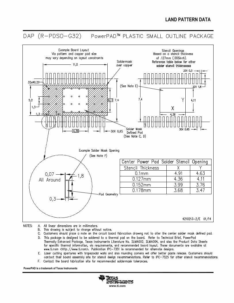
EXAMPLE BOARD LAYOUT
(7.5)
0.05 MAXAROUND
0.05 MINAROUND
32X (1.5)
32X (0.45)
30X (0.65)
(R ) TYP0.05
PowerPAD TSSOP - 1.2 mm max heightDAD0032APLASTIC SMALL OUTLINE
4222646/A 12/2015
SYMM
SYMM
SEE DETAILS
LAND PATTERN EXAMPLESCALE:8X
1
16 17
32
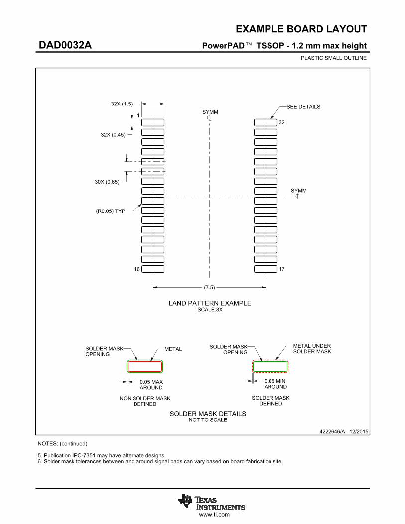
NOTES: (continued) 5. Publication IPC-7351 may have alternate designs. 6. Solder mask tolerances between and around signal pads can vary based on board fabrication site.
TM
METALSOLDER MASKOPENING
NON SOLDER MASKDEFINED
SOLDER MASK DETAILSNOT TO SCALE
OPENINGSOLDER MASK METAL UNDER
SOLDER MASK
SOLDER MASKDEFINED

www.ti.com
EXAMPLE STENCIL DESIGN
32X (1.5)
32X (0.45)
(7.5)
30X (0.65)
(R ) TYP0.05
PowerPAD TSSOP - 1.2 mm max heightDAD0032APLASTIC SMALL OUTLINE
4222646/A 12/2015
NOTES: (continued) 7. Laser cutting apertures with trapezoidal walls and rounded corners may offer better paste release. IPC-7525 may have alternate design recommendations. 8. Board assembly site may have different recommendations for stencil design.
TM
SOLDER PASTE EXAMPLEBASED ON 0.125 mm THICK STENCIL
SCALE:8X
SYMM
SYMM
1
16 17
32

IMPORTANT NOTICE
Texas Instruments Incorporated and its subsidiaries (TI) reserve the right to make corrections, enhancements, improvements and otherchanges to its semiconductor products and services per JESD46, latest issue, and to discontinue any product or service per JESD48, latestissue. Buyers should obtain the latest relevant information before placing orders and should verify that such information is current andcomplete. All semiconductor products (also referred to herein as “components”) are sold subject to TI’s terms and conditions of salesupplied at the time of order acknowledgment.TI warrants performance of its components to the specifications applicable at the time of sale, in accordance with the warranty in TI’s termsand conditions of sale of semiconductor products. Testing and other quality control techniques are used to the extent TI deems necessaryto support this warranty. Except where mandated by applicable law, testing of all parameters of each component is not necessarilyperformed.TI assumes no liability for applications assistance or the design of Buyers’ products. Buyers are responsible for their products andapplications using TI components. To minimize the risks associated with Buyers’ products and applications, Buyers should provideadequate design and operating safeguards.TI does not warrant or represent that any license, either express or implied, is granted under any patent right, copyright, mask work right, orother intellectual property right relating to any combination, machine, or process in which TI components or services are used. Informationpublished by TI regarding third-party products or services does not constitute a license to use such products or services or a warranty orendorsement thereof. Use of such information may require a license from a third party under the patents or other intellectual property of thethird party, or a license from TI under the patents or other intellectual property of TI.Reproduction of significant portions of TI information in TI data books or data sheets is permissible only if reproduction is without alterationand is accompanied by all associated warranties, conditions, limitations, and notices. TI is not responsible or liable for such altereddocumentation. Information of third parties may be subject to additional restrictions.Resale of TI components or services with statements different from or beyond the parameters stated by TI for that component or servicevoids all express and any implied warranties for the associated TI component or service and is an unfair and deceptive business practice.TI is not responsible or liable for any such statements.Buyer acknowledges and agrees that it is solely responsible for compliance with all legal, regulatory and safety-related requirementsconcerning its products, and any use of TI components in its applications, notwithstanding any applications-related information or supportthat may be provided by TI. Buyer represents and agrees that it has all the necessary expertise to create and implement safeguards whichanticipate dangerous consequences of failures, monitor failures and their consequences, lessen the likelihood of failures that might causeharm and take appropriate remedial actions. Buyer will fully indemnify TI and its representatives against any damages arising out of the useof any TI components in safety-critical applications.In some cases, TI components may be promoted specifically to facilitate safety-related applications. With such components, TI’s goal is tohelp enable customers to design and create their own end-product solutions that meet applicable functional safety standards andrequirements. Nonetheless, such components are subject to these terms.No TI components are authorized for use in FDA Class III (or similar life-critical medical equipment) unless authorized officers of the partieshave executed a special agreement specifically governing such use.Only those TI components which TI has specifically designated as military grade or “enhanced plastic” are designed and intended for use inmilitary/aerospace applications or environments. Buyer acknowledges and agrees that any military or aerospace use of TI componentswhich have not been so designated is solely at the Buyer's risk, and that Buyer is solely responsible for compliance with all legal andregulatory requirements in connection with such use.TI has specifically designated certain components as meeting ISO/TS16949 requirements, mainly for automotive use. In any case of use ofnon-designated products, TI will not be responsible for any failure to meet ISO/TS16949.
Products ApplicationsAudio www.ti.com/audio Automotive and Transportation www.ti.com/automotiveAmplifiers amplifier.ti.com Communications and Telecom www.ti.com/communicationsData Converters dataconverter.ti.com Computers and Peripherals www.ti.com/computersDLP® Products www.dlp.com Consumer Electronics www.ti.com/consumer-appsDSP dsp.ti.com Energy and Lighting www.ti.com/energyClocks and Timers www.ti.com/clocks Industrial www.ti.com/industrialInterface interface.ti.com Medical www.ti.com/medicalLogic logic.ti.com Security www.ti.com/securityPower Mgmt power.ti.com Space, Avionics and Defense www.ti.com/space-avionics-defenseMicrocontrollers microcontroller.ti.com Video and Imaging www.ti.com/videoRFID www.ti-rfid.comOMAP Applications Processors www.ti.com/omap TI E2E Community e2e.ti.comWireless Connectivity www.ti.com/wirelessconnectivity
Mailing Address: Texas Instruments, Post Office Box 655303, Dallas, Texas 75265Copyright © 2016, Texas Instruments Incorporated