16-bit mcu and dsc programmer's reference manual - microchip
TRANSCRIPT

© 2005-2011 Microchip Technology Inc. DS70157F
16-bit MCU and DSC Programmer’s Reference ManualHigh-Performance Microcontrollers (MCU)
and Digital Signal Controllers (DSC)

Note the following details of the code protection feature on Microchip devices:• Microchip products meet the specification contained in their particular Microchip Data Sheet.
• Microchip believes that its family of products is one of the most secure families of its kind on the market today, when used in the intended manner and under normal conditions.
• There are dishonest and possibly illegal methods used to breach the code protection feature. All of these methods, to our knowledge, require using the Microchip products in a manner outside the operating specifications contained in Microchip’s Data Sheets. Most likely, the person doing so is engaged in theft of intellectual property.
• Microchip is willing to work with the customer who is concerned about the integrity of their code.
• Neither Microchip nor any other semiconductor manufacturer can guarantee the security of their code. Code protection does not mean that we are guaranteeing the product as “unbreakable.”
Code protection is constantly evolving. We at Microchip are committed to continuously improving the code protection features of our products. Attempts to break Microchip’s code protection feature may be a violation of the Digital Millennium Copyright Act. If such acts allow unauthorized access to your software or other copyrighted work, you may have a right to sue for relief under that Act.
Information contained in this publication regarding device applications and the like is provided only for your convenience and may be superseded by updates. It is your responsibility to ensure that your application meets with your specifications. MICROCHIP MAKES NO REPRESENTATIONS OR WARRANTIES OF ANY KIND WHETHER EXPRESS OR IMPLIED, WRITTEN OR ORAL, STATUTORY OR OTHERWISE, RELATED TO THE INFORMATION, INCLUDING BUT NOT LIMITED TO ITS CONDITION, QUALITY, PERFORMANCE, MERCHANTABILITY OR FITNESS FOR PURPOSE. Microchip disclaims all liability arising from this information and its use. Use of Microchip devices in life support and/or safety applications is entirely at the buyer’s risk, and the buyer agrees to defend, indemnify and hold harmless Microchip from any and all damages, claims, suits, or expenses resulting from such use. No licenses are conveyed, implicitly or otherwise, under any Microchip intellectual property rights.
DS70157F-page 2
Trademarks
The Microchip name and logo, the Microchip logo, dsPIC, KEELOQ, KEELOQ logo, MPLAB, PIC, PICmicro, PICSTART, PIC32 logo, rfPIC and UNI/O are registered trademarks of Microchip Technology Incorporated in the U.S.A. and other countries.
FilterLab, Hampshire, HI-TECH C, Linear Active Thermistor, MXDEV, MXLAB, SEEVAL and The Embedded Control Solutions Company are registered trademarks of Microchip Technology Incorporated in the U.S.A.
Analog-for-the-Digital Age, Application Maestro, chipKIT, chipKIT logo, CodeGuard, dsPICDEM, dsPICDEM.net, dsPICworks, dsSPEAK, ECAN, ECONOMONITOR, FanSense, HI-TIDE, In-Circuit Serial Programming, ICSP, Mindi, MiWi, MPASM, MPLAB Certified logo, MPLIB, MPLINK, mTouch, Omniscient Code Generation, PICC, PICC-18, PICDEM, PICDEM.net, PICkit, PICtail, REAL ICE, rfLAB, Select Mode, Total Endurance, TSHARC, UniWinDriver, WiperLock and ZENA are trademarks of Microchip Technology Incorporated in the U.S.A. and other countries.
SQTP is a service mark of Microchip Technology Incorporated in the U.S.A.
All other trademarks mentioned herein are property of their respective companies.
© 2005-2011, Microchip Technology Incorporated, Printed in the U.S.A., All Rights Reserved.
Printed on recycled paper.
ISBN: 978-1-61341-357-9
© 2005-2011 Microchip Technology Inc.
Microchip received ISO/TS-16949:2009 certification for its worldwide headquarters, design and wafer fabrication facilities in Chandler and Tempe, Arizona; Gresham, Oregon and design centers in California and India. The Company’s quality system processes and procedures are for its PIC® MCUs and dsPIC® DSCs, KEELOQ® code hopping devices, Serial EEPROMs, microperipherals, nonvolatile memory and analog products. In addition, Microchip’s quality system for the design and manufacture of development systems is ISO 9001:2000 certified.

Table of Contents
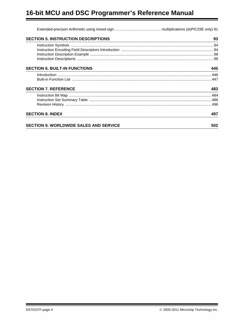
PAGESECTION 1. INTRODUCTION 5
Introduction ......................................................................................................................................................... 6Manual Objective ................................................................................................................................................ 6Development Support ......................................................................................................................................... 6Style and Symbol Conventions ........................................................................................................................... 7Instruction Set Symbols ...................................................................................................................................... 8
SECTION 2. PROGRAMMER’S MODEL 916-bit MCU and DSC Core Architecture Overview ............................................................................................ 10Programmer’s Model ......................................................................................................................................... 14Working Register Array ..................................................................................................................................... 18Default Working Register (WREG) .................................................................................................................... 18Software Stack Frame Pointer .......................................................................................................................... 18Software Stack Pointer ...................................................................................................................................... 19Stack Pointer Limit Register (SPLIM) ................................................................................................................ 19Accumulator A and Accumulator B (dsPIC30F, dsPIC33F and dsPIC33E Devices) ........................................ 19Program Counter ............................................................................................................................................... 19TBLPAG Register .............................................................................................................................................. 19PSVPAG Register (PIC24F, PIC24H, dsPIC30F and dsPIC33F) ..................................................................... 19RCOUNT Register ............................................................................................................................................ 20DCOUNT Register (dsPIC30F, dsPIC33F and dsPIC33E Devices) ................................................................. 20DOSTART Register (dsPIC30F, dsPIC33F and dsPIC33E Devices) ............................................................... 20DOEND Register (dsPIC30F, dsPIC33F and dsPIC33E Devices) .................................................................... 21STATUS Register .............................................................................................................................................. 21Core Control Register ....................................................................................................................................... 24Shadow Registers ............................................................................................................................................. 24DO Stack (dsPIC33E Devices) .......................................................................................................................... 25
SECTION 3. INSTRUCTION SET OVERVIEW 37Introduction ....................................................................................................................................................... 38Instruction Set Overview ................................................................................................................................... 38Instruction Set Summary Tables ....................................................................................................................... 40
SECTION 4. INSTRUCTION SET DETAILS 51Data Addressing Modes .................................................................................................................................... 52Program Addressing Modes .............................................................................................................................. 61Instruction Stalls ................................................................................................................................................ 62Byte Operations ................................................................................................................................................ 64Word Move Operations ..................................................................................................................................... 66Using 10-bit Literal Operands ........................................................................................................................... 69Software Stack Pointer and Frame Pointer ....................................................................................................... 70Conditional Branch Instructions ........................................................................................................................ 76Z Status Bit ........................................................................................................................................................ 77Assigned Working Register Usage .................................................................................................................... 78DSP Data Formats (dsPIC30F, dsPIC33F and dsPIC33E Devices) ................................................................. 81Accumulator Usage (dsPIC30F, dsPIC33F and dsPIC33E Devices) ................................................................ 83Accumulator Access (dsPIC30F, dsPIC33F and dsPIC33E Devices) .............................................................. 84DSP MAC Instructions (dsPIC30F, dsPIC33F and dsPIC33E Devices) ........................................................... 84DSP Accumulator Instructions (dsPIC30F, dsPIC33F and dsPIC33E Devices) ............................................... 88Scaling Data with the FBCL Instruction (dsPIC30F, dsPIC33F and dsPIC33E Devices) ................................. 88Normalizing the Accumulator with the FBCL Instruction (dsPIC30F, dsPIC33F and dsPIC33E Devices) ........ 90
© 2005-2011 Microchip Technology Inc. DS70157F-page 3
16-bit MCU and DSC Programmer’s Reference Manual
Extended-precison Arithmetic using mixed-sign ............................................. multiplications (dsPIC33E only) 91
SECTION 5. INSTRUCTION DESCRIPTIONS 93Instruction Symbols ........................................................................................................................................... 94Instruction Encoding Field Descriptors Introduction .......................................................................................... 94Instruction Description Example ........................................................................................................................ 98Instruction Descriptions ..................................................................................................................................... 99
SECTION 6. BUILT-IN FUNCTIONS 445Introduction ...................................................................................................................................................... 446Built-in Function List ........................................................................................................................................ 447
SECTION 7. REFERENCE 483Instruction Bit Map ........................................................................................................................................... 484Instruction Set Summary Table ....................................................................................................................... 486Revision History .............................................................................................................................................. 496
SECTION 8. INDEX 497
SECTION 9. WORLDWIDE SALES AND SERVICE 502
DS70157F-page 4 © 2005-2011 Microchip Technology Inc.

Introduction
1
Section 1. Introduction
HIGHLIGHTSThis section of the manual contains the following major topics:
1.1 Introduction ....................................................................................................................... 61.2 Manual Objective .............................................................................................................. 61.3 Development Support ....................................................................................................... 61.4 Style and Symbol Conventions ......................................................................................... 71.5 Instruction Set Symbols .................................................................................................... 8
© 2005-2011 Microchip Technology Inc. DS70157F-page 5

16-bit MCU and DSC Programmer’s Reference Manual
1.1 INTRODUCTIONMicrochip Technology focuses on products for the embedded control market. Microchip is a leading supplier of the following devices and products:
• 8-bit General Purpose Microcontrollers (PIC® MCUs)• 16-bit Digital Signal Controllers (dsPIC® DSCs)• 16-bit and 32-bit Microcontrollers (MCUs)• Speciality and Standard Nonvolatile Memory Devices• Security Devices (KEELOQ® Security ICs)• Application-specific Standard ProductsInformation about these devices and products, with corresponding technical documentation, is available on the Microchip web site (www.microchip.com).
1.2 MANUAL OBJECTIVEThis manual is a software developer’s reference for the 16-bit MCU and DSC device families. It describes the Instruction Set in detail and also provides general information to assist the development of software for the 16-bit MCU and DSC device families.
This manual does not include detailed information about the core, peripherals, system integration or device-specific information. The user should refer to the specific device family reference manual for information about the core, peripherals and system integration. For device-specific information, the user should refer to the specific device data sheets. The information that can be found in the data sheets includes:
• Device memory map• Device pinout and packaging details• Device electrical specifications• List of peripherals included on the deviceCode examples are given throughout this manual. These examples are valid for any device in the 16-bit MCU and DSC families.
1.3 DEVELOPMENT SUPPORTMicrochip offers a wide range of development tools that allow users to efficiently develop and debug application code. Microchip’s development tools can be broken down into four categories:
• Code generation• Hardware/Software debug• Device programmer• Product evaluation boardsInformation about the latest tools, product briefs and user guides can be obtained from the Microchip web site (www.microchip.com) or from your local Microchip Sales Office.
Microchip offers other reference tools to speed the development cycle. These include:
• Application Notes • Reference Designs • Microchip web site • Local Sales Offices with Field Application Support • Corporate Support Line The Microchip web site also lists other sites that may be useful references.
DS70157F-page 6 © 2005-2011 Microchip Technology Inc.

Section 1. IntroductionIntroduction
1
1.4 STYLE AND SYMBOL CONVENTIONSThroughout this document, certain style and font format conventions are used. Table 1-1 provides a description of the conventions used in this document.
Table 1-1: Document Conventions
Symbol or Term Description
set To force a bit/register to a value of logic ‘1’.clear To force a bit/register to a value of logic ‘0’.Reset 1. To force a register/bit to its default state.
2. A condition in which the device places itself after a device Reset occurs. Some bits will be forced to ‘0’ (such as interrupt enable bits), while others will be forced to ‘1’ (such as the I/O data direction bits).
0xnnnn Designates the number ‘nnnn’ in the hexadecimal number system. These conventions are used in the code examples. For example, 0x013F or 0xA800.
: (colon) Used to specify a range or the concatenation of registers/bits/pins. One example is ACCAU:ACCAH:ACCAL, which is the concatenation of three registers to form the 40-bit Accumulator. Concatenation order (left-right) usually specifies a positional relationship (MSb to LSb, higher to lower).
< > Specifies bit locations in a particular register. One example is SR<7:5> (or IPL<2:0>), which specifies the register and associated bits or bit locations.
LSb, MSb Indicates the Least Significant or Most Significant bit in a field.LSB, MSB Indicates the Least/Most Significant Byte in a field of bits.lsw, msw Indicates the least/most significant word in a field of bitsCourier New Font
Used for code examples, binary numbers and for Instruction mnemonics in the text.
Times New Roman Font, Italic
Used for equations and variables.
Times New Roman Font, Bold Italic
Used in explanatory text for items called out from a figure, equation, or example.
Note: A Note presents information that we want to re-emphasize, either to help you avoid a common pitfall, or make you aware of operating differences between some device family members. A Note can be in a box, or when used in a table or figure, it is located at the bottom of the table or figure.
© 2005-2011 Microchip Technology Inc. DS70157F-page 7

16-bit MCU and DSC Programmer’s Reference Manual
1.5 INSTRUCTION SET SYMBOLSThe summary tables in Section 3.2 “Instruction Set Overview” and Section 7.2 “Instruction Set Summary Table”, and the instruction descriptions in Section 5.4 “Instruction Descriptions” utilize the symbols shown in Table 1-2.
Table 1-2: Symbols Used in Instruction Summary Tables and Descriptions
Symbol(1) Description
{ } Optional field or operation[text] The location addressed by text(text) The contents of text#text The literal defined by texta ∈ [b, c, d] “a” must be in the set of [b, c, d]<n:m> Register bit field{label:} Optional label nameAcc Accumulator A or Accumulator BAWB Accumulator Write Backbit4 4-bit wide bit position (0:7 in Byte mode, 0:15 in Word mode)Expr Absolute address, label or expression (resolved by the linker)f File register addresslit1 1-bit literal (0:1)lit4 4-bit literal (0:15)lit5 5-bit literal (0:31)lit8 8-bit literal (0:255)lit10 10-bit literal (0:255 in Byte mode, 0:1023 in Word mode)lit14 14-bit literal (0:16383)lit16 16-bit literal (0:65535)lit23 23-bit literal (0:8388607)Slit4 Signed 4-bit literal (-8:7)Slit6 Signed 6-bit literal (-32:31) (range is limited to -16:16)Slit10 Signed 10-bit literal (-512:511)Slit16 Signed 16-bit literal (-32768:32767)TOS Top-of-StackWb Base working register Wd Destination working register (direct and indirect addressing)Wdo Destination working register (direct and indirect addressing, including indirect addressing with offset)Wm, Wn Working register divide pair (dividend, divisor)Wm * Wm Working register multiplier pair (same source register)Wm * Wn Working register multiplier pair (different source registers)Wn Both source and destination working register (direct addressing)Wnd Destination working register (direct addressing)Wns Source working register (direct addressing)WREG Default working register (assigned to W0)Ws Source working register (direct and indirect addressing)Wso Source working register (direct and indirect addressing, including indirect addressing with offset)Wx Source Addressing mode and working register for X data bus prefetchWxd Destination working register for X data bus prefetch Wy Source Addressing mode and working register for Y data bus prefetchWyd Destination working register for Y data bus prefetchNote 1: The range of each symbol is instruction dependent. Refer to Section 5. “Instruction Descriptions” for
the specific instruction range.
DS70157F-page 8 © 2005-2011 Microchip Technology Inc.

Section 2. Programmer’s Model
Programm
er’s M
odel
2
HIGHLIGHTSThis section of the manual contains the following major topics:
2.1 16-bit MCU and DSC Core Architecture Overview ......................................................... 102.2 Programmer’s Model....................................................................................................... 142.3 Working Register Array................................................................................................... 182.4 Default Working Register (WREG) ................................................................................. 182.5 Software Stack Frame Pointer ........................................................................................ 18
© 2005-2011 Microchip Technology Inc. DS70157F-page 9

16-bit MCU and DSC Programmer’s Reference Manual
2.1 16-BIT MCU AND DSC CORE ARCHITECTURE OVERVIEWThis section provides an overview of the 16-bit architecture features and capabilities for the following families of devices:
• 16-bit Microcontrollers (MCU):- PIC24F- PIC24H- PIC24E
• 16-bit Digital Signal Controllers (DSC):- dsPIC30F- dsPIC33F- dsPIC33E
2.1.1 Features Specific to 16-bit MCU and DSC CoreThe core of the 16-bit MCU and DSC devices is a 16-bit (data) modified Harvard architecture with an enhanced instruction set. The core has a 24-bit instruction word, with an 8-bit Op code field. The Program Counter (PC) is 23 bits wide and addresses up to 4M x 24 bits of user program memory space. An instruction prefetch mechanism is used to help maintain throughput and provides predictable execution. The majority of instructions execute in a single cycle.
2.1.1.1 REGISTERS
The 16-bit MCU and DSC devices have sixteen 16-bit working registers. Each of the working registers can act as a data, address or offset register. The 16th working register (W15) operates as a software Stack Pointer for interrupts and calls.
2.1.1.2 INSTRUCTION SET
The instruction set is almost identical for the 16-bit MCU and DSC architectures. The instruction set includes many Addressing modes and was designed for optimum C compiler efficiency.
2.1.1.3 DATA SPACE ADDRESSING
The data space can be addressed as 32K words or 64 Kbytes. The upper 32 Kbytes of the data space memory map can optionally be mapped into program space at any 16K program word boundary, which is a feature known as Program Space Visibility (PSV). The program to data space mapping feature lets any instruction access program space as if it were the data space, which is useful for storing data coefficients.
2.1.1.4 ADDRESSING MODES
The core supports Inherent (no operand), Relative, Literal, Memory Direct, Register Direct, Register Indirect, and Register Offset Addressing modes. Each instruction is associated with a predefined Addressing mode group, depending upon its functional requirements. As many as seven Addressing modes are supported for each instruction.
For most instructions, the CPU is capable of executing a data (or program data) memory read, a working register (data) read, a data memory write and a program (instruction) memory read per instruction cycle. As a result, 3-operand instructions can be supported, allowing A + B = C operations to be executed in a single cycle.
Note: Some devices families support Extended Data Space (EDS) addressing. See the specific device data sheet and family reference manual for more details on this feature.
DS70157F-page 10 © 2005-2011 Microchip Technology Inc.

Section 2. Programmer’s ModelProgram
mer’s
Model
2
2.1.1.5 ARITHMETIC AND LOGIC UNIT
A high-speed, 17-bit by 17-bit multiplier is included to significantly enhance the core’s arithmetic capability and throughput. The multiplier supports Signed, Unsigned, and Mixed modes, as well as 16-bit by 16-bit, or 8-bit by 8-bit integer multiplication. All multiply instructions execute in a single cycle.
The 16-bit Arithmetic Logic Unit (ALU) is enhanced with integer divide assist hardware that supports an iterative non-restoring divide algorithm. It operates in conjunction with the REPEATinstruction looping mechanism, and a selection of iterative divide instructions, to support 32-bit (or 16-bit) divided by 16-bit integer signed and unsigned division. All divide operations require 19 cycles to complete, but are interruptible at any cycle boundary.
2.1.1.6 EXCEPTION PROCESSING
The 16-bit MCU and DSC devices have a vectored exception scheme with support for up to 8 sources of non-maskable traps and up to 246 interrupt sources. In both families, each interrupt source can be assigned to one of seven priority levels.
2.1.2 PIC24E and dsPIC33E FeaturesIn addition to the information provided in Section 2.1.1 “Features Specific to 16-bit MCU and DSC Core”, this section describes the enhancements that are available in the PIC24E and dsPIC33E families of devices.
2.1.2.1 DATA SPACE ADDRESSING
The Base Data Space address is used in conjunction with a read or write page register (DSRPAG or DSWPAG) to form an Extended Data Space (EDS) address, which can also be used for PSV access. The EDS can be addressed as 8 M words or 16 Mbytes. Refer to Section 3. “Data Memory” (DS70595) in the “dsPIC33E/PIC24E Family Reference Manual” for more details on EDS, PSV, and table accesses.
2.1.2.2 AUTOMATIC MIXED-SIGN MULTIPLICATION MODE (dsPIC33E ONLY)
In addition to signed and unsigned DSP multiplications, dsPIC33E devices support mixed-sign (unsigned-signed and signed-unsigned) multiplications without the need to dynamically reconfigure the multiplication mode and shift data to account for the difference in operand formats. This mode is particularly beneficial for executing extended-precision (32-bit and 64-bit) algorithms. Besides DSP instructions, MCU multiplication (MUL) instructions can also utilize either accumulator as a result destination, thereby enabling faster extended-precision arithmetic. Refer to 4.10.1 “Implied DSP Operands (dsPIC30F, dsPIC33F and dsPIC33E Devices)” and 4.18 “Extended-precison Arithmetic using mixed-sign multiplications (dsPIC33E only)” for more details on mixed-sign DSP multiplications.
2.1.2.3 MCU MULTIPLICATIONS WITH 16-BIT RESULT
16x16-bit MUL instructions include an option to store the product in a single 16-bit working register rather than a pair of registers. This feature helps free up a register for other purposes, in cases where the numbers being multiplied are small in magnitude and therefore expected to provide a 16-bit result. See the individual MUL instruction descriptions in 5.4 “Instruction Descriptions” for more details.
2.1.2.4 HARDWARE STACK FOR DO LOOPS (dsPIC33E ONLY)
The single-level DO loop shadow register-set has been replaced by 4-level deep DO loop hardware stack. This provides automatic DO loop register save/restore for up to 3 levels of DO loop nesting, resulting in more efficient implementation of nested loops. Refer to 2.19 “DO Stack (dsPIC33E Devices)” for more details on DO loop nesting in dsPIC33E devices.
Note: Some PIC24F devices also support Extended Data Space. Refer to Section 44. “CPU with EDS” (DS39732) and Section 45. “Data Memory with EDS” (DS39733) of the PIC24F Family Reference Manual for details.
© 2005-2011 Microchip Technology Inc. DS70157F-page 11

16-bit MCU and DSC Programmer’s Reference Manual
2.1.2.5 DSP CONTEXT SWITCH SUPPORT (dsPIC33E ONLY)
In dsPIC33E devices, the DSP overflow and saturation status bits are writable. This allows the state of the DSP Engine to be efficiently saved and restored while switching between DSP tasks. See 2.16.4 “DSP ALU Status Bits (dsPIC30F, dsPIC33F and dsPIC33E Devices)” for more details on DSP status bits.
2.1.2.6 EXTENDED CALL AND GOTO INSTRUCTIONS
The new CALL.L Wn and GOTO.L Wn instructions extend the capabilities of the CALL Wn and GOTO Wn by enabling 32-bit addresses for computed branch/call destinations. In these enhanced instructions, the destination address is provided by a pair of working registers rather than a single 16-bit register. See the CALL.L and GOTO.L instruction descriptions in 5.4 “Instruction Descriptions” for more details.
2.1.2.7 COMPARE-BRANCH INSTRUCTIONS
dsPIC33E/PIC24E devices feature conditional Compare-Branch (CPBxx) instructions. These instructions extend the capabilities of the Compare-Skip (CPSxx) instructions by allowing branches rather than only skipping over a single instruction. See the CPBEQ, CPBNE, CPBGT and CPBLT instruction descriptions in 5.4 “Instruction Descriptions” for more details on compare-branch instructions.
2.1.3 dsPIC30F, dsPIC33F, and dsPIC33E FeaturesIn addition to the information provided in Section 2.1.1 “Features Specific to 16-bit MCU and DSC Core”, this section describes the DSP enhancements that are available in the dsPIC30F, dsPIC33F, and dsPIC33E families of devices.
2.1.3.1 PROGRAMMING LOOP CONSTRUCTS
Overhead free program loop constructs are supported using the DO instruction, which is interruptible.
2.1.3.2 DSP INSTRUCTION CLASS
The DSP class of instructions.are seamlessly integrated into the architecture and execute from a single execution unit.
2.1.3.3 DATA SPACE ADDRESSING
The data space is split into two blocks, referred to as X and Y data memory. Each memory block has its own independent Address Generation Unit (AGU). The MCU class of instructions operate solely through the X memory AGU, which accesses the entire memory map as one linear data space. The DSP dual source class of instructions operates through the X and Y AGUs, which splits the data address space into two parts. The X and Y data space boundary is arbitrary and device-specific.
2.1.3.4 MODULO AND BIT-REVERSED ADDRESSING
Overhead-free circular buffers (modulo addressing) are supported in both X and Y address spaces. The modulo addressing removes the software boundary checking overhead for DSP algorithms. Furthermore, the X AGU circular addressing can be used with any of the MCU class of instructions. The X AGU also supports bit-reverse addressing, to greatly simplify input or output data reordering for radix-2 FFT algorithms.
2.1.3.5 DSP ENGINE
The DSP engine features a high-speed, 17-bit by 17-bit multiplier, a 40-bit ALU, two 40-bit saturating accumulators and a 40-bit bidirectional barrel shifter. The barrel shifter is capable of shifting a 40-bit value, up to 16 bits right, or up to 16 bits left, in a single cycle. The DSP instructions operate seamlessly with all other instructions and have been designed for optimal real-time performance. The MAC instruction and other associated instructions can concurrently fetch two data operands from memory while multiplying two working registers. This requires that
DS70157F-page 12 © 2005-2011 Microchip Technology Inc.

Section 2. Programmer’s ModelProgram
mer’s
Model
2
the data space be split for these instructions and linear for all others. This is achieved in a transparent and flexible manner through dedicating certain working registers to each address space.
2.1.3.6 EXCEPTION PROCESSING
The dsPIC30F devices have a vectored exception scheme with support for up to 8 sources of non-maskable traps and up to 54 interrupt sources. The dsPIC33F and dsPIC33E have a similar exception scheme, but support up to 118, and up to 246 interrupt sources, respectively. In all three families, each interrupt source can be assigned to one of seven priority levels.
Refer to Section 6 and 28 “ Interrupts” of the dsPIC30F Family Reference Manual, Sections 6, 29,32, 41, 47 and 53 of the dsPIC33F/PIC24H Family Reference Manual and Section 6 of the dsPIC33E/PIC24E Family Reference Manual, for more details on Exception Processing.
© 2005-2011 Microchip Technology Inc. DS70157F-page 13

16-bit MCU and DSC Programmer’s Reference Manual
2.2 PROGRAMMER’S MODELFigure 2-1 through Figure 2-4 show the programmer’s model diagrams for the 16-bit MCU and DSC families of devices.
Figure 2-1: PIC24F and PIC24H Programmer’s Model Diagram
TABPAG
22 0
7 0
015
Program Counter
Data Table Page Address
Status Register
Working Registers
W1
W2
W3
W4
W5
W6
W7
W8
W9
W10
W11
W12
W13
W14/Frame Pointer
W15/Stack Pointer
PSVPAG7 0
Program Space Visibility Page Address
Z— — — —
RCOUNT
13 0REPEAT Loop Counter
IPL2 IPL1
SPLIM Stack Pointer Limit Register
SRL
— —
15 0CPU Core Control Register CORCON
— DC RA N C
TBLPAG
PSVPAG
IPL0 OV
W0/WREG
SRH
DIV and MULResult Registers
0
PUSH.S
Legend
Shadow Register
DS70157F-page 14 © 2005-2011 Microchip Technology Inc.
Section 2. Programmer’s ModelProgram
mer’s
Model
2
Figure 2-2: PIC24E Programmer’s Model Diagram
TABPAG
22 0
7 0
015
Program Counter
Data Table Page Address
Status Register
Working Registers
W1
W2
W3
W4
W5
W6
W7
W8
W9
W10
W11
W12
W13
W14/Frame Pointer
W15/Stack Pointer
PSVPAG9 0
Data Space Read Page Address
Z— — — —
RCOUNT
15 0REPEAT Loop Counter
IPL2 IPL1
SPLIM Stack Pointer Limit Register
SRL
PUSH.S and
— —
15 0CPU Core Control Register
Legend
CORCON
— DC RA N C
TBLPAG
DSRPAG
IPL0 OV
W0/WREG
SRH
DIV and MULResult Registers
0
POP.S Shadow Registers
PSVPAG8 0
Data Space Write Page AddressDSWPAG
© 2005-2011 Microchip Technology Inc. DS70157F-page 15

16-bit MCU and DSC Programmer’s Reference Manual
Figure 2-3: dsPIC30F and dsPIC33F Programmer’s Model Diagram
TABPAG
22 0
7 0
015
Program Counter
Data Table Page Address
Status Register
Working Registers
W1
W2
W3
W4
W5
W6
W7
W8
W9
W10
W11
W12
W13
W14/Frame Pointer
W15/Stack Pointer
PSVPAG7 0
Program Space Visibility Page Address
ZOA OB SA SB
RCOUNT
13 0REPEAT Loop Counter
IPL2 IPL1
SPLIM Stack Pointer Limit Register
SRL
OAB SAB
13 0DO Loop Counter DCOUNT
DA DC RA N C
TBLPAG
PSVPAG
IPL0 OV
W0/WREG
SRH
DIV and MULResult Registers
0
PUSH.S
Legend
Shadow Register
DO Shadow Register
39 031
DSPAccumulators
ACCA
ACCB
15
DOSTART
24 0DO Loop Start Address
15 0CPU Core Control Register CORCON
DO Loop End AddressDOEND
24 0
00
00
MAC OperandRegisters
MAC AddressRegisters
DS70157F-page 16 © 2005-2011 Microchip Technology Inc.

Section 2. Programmer’s ModelProgram
mer’s
Model
2
Figure 2-4: dsPIC33E Programmer’s Model Diagram
RCOUNT
15 0REPEAT Loop Counter
15 0DO Loop Counter DCOUNT
DOSTART
24 0DO Loop Start Address
15 0CPU Core Control Register CORCON
DO Loop End AddressDOEND
24 0
00
00
015
Working Registers
W1
W2
W3
W4
W5
W6
W7
W8
W9
W10
W11
W12
W13
W14/Frame Pointer
W15/Stack Pointer
SPLIM Stack Pointer Limit Register
W0/WREGDIV and MULResult Registers
Legend
Nested DO
39 031
DSPAccumulators
ACCA
ACCB
15
MAC OperandRegisters
MAC AddressRegisters
Status RegisterZIPL2 IPL1
SRL
RA N CIPL0 OV
SRH
Stack
PUSH.S and POP.S Shadow Registers
TABPAG
22 0
7 0
Program Counter
Data Table Page Address
PSVPAG9 0
X Data Space Read Page Address
TBLPAG
DSRPAG
0
PSVPAG8 0
X Data Space Write Page AddressDSWPAG
OA OB SA SB OAB SAB DA DC
© 2005-2011 Microchip Technology Inc. DS70157F-page 17
16-bit MCU and DSC Programmer’s Reference Manual
All registers in the programmer’s model are memory mapped and can be manipulated directly by the instruction set. A description of each register is provided in Table 2-1.
2.3 WORKING REGISTER ARRAYThe 16 working (W) registers can function as data, address or offset registers. The function of a W register is determined by the instruction that accesses it.
Byte instructions, which target the working register array, only affect the Least Significant Byte (LSB) of the target register. Since the working registers are memory mapped, the Least and Most Significant Bytes can be manipulated through byte-wide data memory space accesses.
2.4 DEFAULT WORKING REGISTER (WREG)The instruction set can be divided into two instruction types: working register instructions and file register instructions. The working register instructions use the working register array as data values or as addresses that point to a memory location. In contrast, file register instructions operate on a specific memory address contained in the instruction opcode.
File register instructions that also utilize a working register do not specify the working register that is to be used for the instruction. Instead, a default working register (WREG) is used for these file register instructions. Working register, W0, is assigned to be the WREG. The WREG assignment is not programmable.
2.5 SOFTWARE STACK FRAME POINTERA frame is a user-defined section of memory in the stack, used by a function to allocate memory for local variables. W14 has been assigned for use as a Stack Frame Pointer with the link (LNK)and unlink (ULNK) instructions. However, if a Stack Frame Pointer and the LNK and ULNKinstructions are not used, W14 can be used by any instruction in the same manner as all other W registers. On dsPIC33E and PIC24E devices, a Stack Frame Active (SFA) Status bit is used to support nested stack frames. See Section 4.7.2 “Software Stack Frame Pointer” for detailed information about the Frame Pointer.
Note: Unless otherwise specified, the Programmer’s Model Register Descriptions in Table 2-1 apply to all MCU and DSC device families.
Table 2-1: Programmer’s Model Register Descriptions
Register Description
CORCON CPU Core Configuration registerPC 23-bit Program CounterPSVPAG(1) Program Space Visibility Page Address registerDSRPAG(2) Extended Data Space (EDS) Read Page registerDSWPAG(2) Extended Data Space (EDS) Write Page registerRCOUNT REPEAT Loop Count registerSPLIM Stack Pointer Limit Value registerSR ALU and DSP Engine STATUS registerTBLPAG Table Memory Page Address registerW0-W15 Working register arrayACCA, ACCB(3) 40-bit DSP AccumulatorsDCOUNT(3) DO Loop Count registerDOSTART(3) DO Loop Start Address registerDOEND(3) DO Loop End Address registerNote 1: This register is only available on PIC24F, PIC24H, dsPIC30F, and dsPIC33F
devices.2: This register is only available on PIC24E and dsPIC33E devices.3: This register is only available on dsPIC30F, dsPIC33F, and dsPIC33E devices.
DS70157F-page 18 © 2005-2011 Microchip Technology Inc.

Section 2. Programmer’s ModelProgram
mer’s
Model
2
2.6 SOFTWARE STACK POINTERW15 serves as a dedicated Software Stack Pointer, and will be automatically modified by function calls, exception processing and returns. However, W15 can be referenced by any instruction in the same manner as all other W registers. This simplifies reading, writing and manipulating the Stack Pointer. Refer to Section 4.7.1 “Software Stack Pointer” for detailed information about the Stack Pointer.
2.7 STACK POINTER LIMIT REGISTER (SPLIM)The SPLIM is a 16-bit register associated with the Stack Pointer. It is used to prevent the Stack Pointer from overflowing and accessing memory beyond the user allocated region of stack memory. Refer to Section 4.7.3 “Stack Pointer Overflow” for detailed information about the SPLIM.
2.8 ACCUMULATOR A AND ACCUMULATOR B (dsPIC30F, dsPIC33F AND dsPIC33E DEVICES)
Accumulator A (ACCA) and Accumulator B (ACCB) are 40-bit wide registers, utilized by DSP instructions to perform mathematical and shifting operations. Each accumulator is composed of 3 memory mapped registers:
• AccxU (bits 39-32)• AccxH (bits 31-16)• AccxL (bits 15-0)
In dsPIC33E devices, Accumulator A and Accumulator B can also be used as destination registers in MCU MUL.xx instructions. This helps reduce the execution time of extended-precision arithmetic operations.
Refer to Section 4.12 “Accumulator Usage (dsPIC30F, dsPIC33F and dsPIC33E Devices)”for details on using ACCA and ACCB.
2.9 PROGRAM COUNTERThe Program Counter (PC) is 23 bits wide. Instructions are addressed in the 4M x 24-bit user program memory space by PC<22:1>, where PC<0> is always set to ‘0’ to maintain instruction word alignment and provide compatibility with data space addressing. This means that during normal instruction execution, the PC increments by 2.
Program memory located at 0x800000 and above is utilized for device configuration data, Unit ID and Device ID. This region is not available for user code execution and the PC can not access this area. However, one may access this region of memory using table instructions. For details on accessing the configuration data, Unit ID, and Device ID, refer to the specific device family reference manual.
2.10 TBLPAG REGISTERThe TBLPAG register is used to hold the upper 8 bits of a program memory address during table read and write operations. Table instructions are used to transfer data between program memory space and data memory space. For details on accessing program memory with the table instructions, refer to the family reference manual of the specific device.
2.11 PSVPAG REGISTER (PIC24F, PIC24H, dsPIC30F AND dsPIC33F)Program space visibility allows the user to map a 32-Kbyte section of the program memory space into the upper 32 Kbytes of data address space. This feature allows transparent access of constant data through instructions that operate on data memory. The PSVPAG register selects the 32-Kbyte region of program memory space that is mapped to the data address space. For details on program space visibility, refer to the specific device family reference manual.
© 2005-2011 Microchip Technology Inc. DS70157F-page 19

16-bit MCU and DSC Programmer’s Reference Manual
2.12 RCOUNT REGISTERThe 14-bit RCOUNT register (16-bit for PIC24E and dsPIC33E devices) register contains the loop counter for the REPEAT instruction. When a REPEAT instruction is executed, RCOUNT is loaded with the repeat count of the instruction, either “lit14” for the “REPEAT #lit14” instruction (“lit15” for the “REPEAT #lit15” instruction for PIC24E and dsPIC33E devices), or the 14 LSb of the Wn register for the “REPEAT Wn” instruction (entire Wn for PIC24E and dsPIC33E devices). The REPEAT loop will be executed RCOUNT + 1 time.
2.13 DCOUNT REGISTER (dsPIC30F, dsPIC33F AND dsPIC33E DEVICES)The 14-bit DCOUNT register (16-bit for dsPIC33E devices) contains the loop counter for hardware DO loops. When a DO instruction is executed, DCOUNT is loaded with the loop count of the instruction, either “lit14” for the “DO #lit14,Expr” instruction (“lit15” for the “DO #lit15,Expr” instruction for dsPIC33E devices) or the 14 LSb of the Ws register for the “DO Ws,Expr” instruction (entire Wn for dsPIC33E devices). The DO loop will be executed DCOUNT + 1 times.
2.14 DOSTART REGISTER (dsPIC30F, dsPIC33F AND dsPIC33E DEVICES)The DOSTART register contains the starting address for a hardware DO loop. When a DO instruction is executed, DOSTART is loaded with the address of the instruction that follows the DO instruction. This location in memory is the start of the DO loop. When looping is activated, program execution continues with the instruction stored at the DOSTART address after the last instruction in the DO loop is executed. This mechanism allows for zero overhead looping.
Note 1: If a REPEAT loop is executing and gets interrupted, RCOUNT may be cleared by the Interrupt Service Routine to break out of the REPEAT loop when the foreground code is re-entered.
2: Refer to the specific device family reference manual for complete details about REPEAT loops.
Note 1: In dsPIC30F and dsPIC33F devices, the DCOUNT register contains a shadow register. See Section 2.18 “Shadow Registers” for information on shadow regis-ters.
2: The dsPIC33E devices have a 4-level-deep, nested DO stack instead of a shadow register.
3: Refer to the specific device family reference manual for complete details about DOloops.
Note 1: For dsPIC30F and dsPIC33F devices, DOSTART has a shadow register. See Section 2.18 “Shadow Registers” for information on shadowing.
2: The dsPIC33E devices have a 4-level-deep, nested DO stack instead of a shadow register. The DOSTART register is read-only in dsPIC33E devices.
3: Refer to the specific device family reference manual for complete details about DOloops.
DS70157F-page 20 © 2005-2011 Microchip Technology Inc.

Section 2. Programmer’s ModelProgram
mer’s
Model
2
2.15 DOEND REGISTER (dsPIC30F, dsPIC33F AND dsPIC33E DEVICES)The DOEND register contains the ending address for a hardware DO loop. When a DO instruction is executed, DOEND is loaded with the address specified by the expression in the DO instruction. This location in memory specifies the last instruction in the DO loop. When looping is activated and the instruction stored at the DOEND address is executed, program execution will continue from the DO loop start address (stored in the DOSTART register).
2.16 STATUS REGISTERThe 16-bit STATUS register maintains status information for the instructions which have been executed most recently. Operation Status bits exist for MCU operations, loop operations and DSP operations. Additionally, the STATUS register contains the CPU Interrupt Priority Level bits, IPL<2:0>, which are used for interrupt processing.
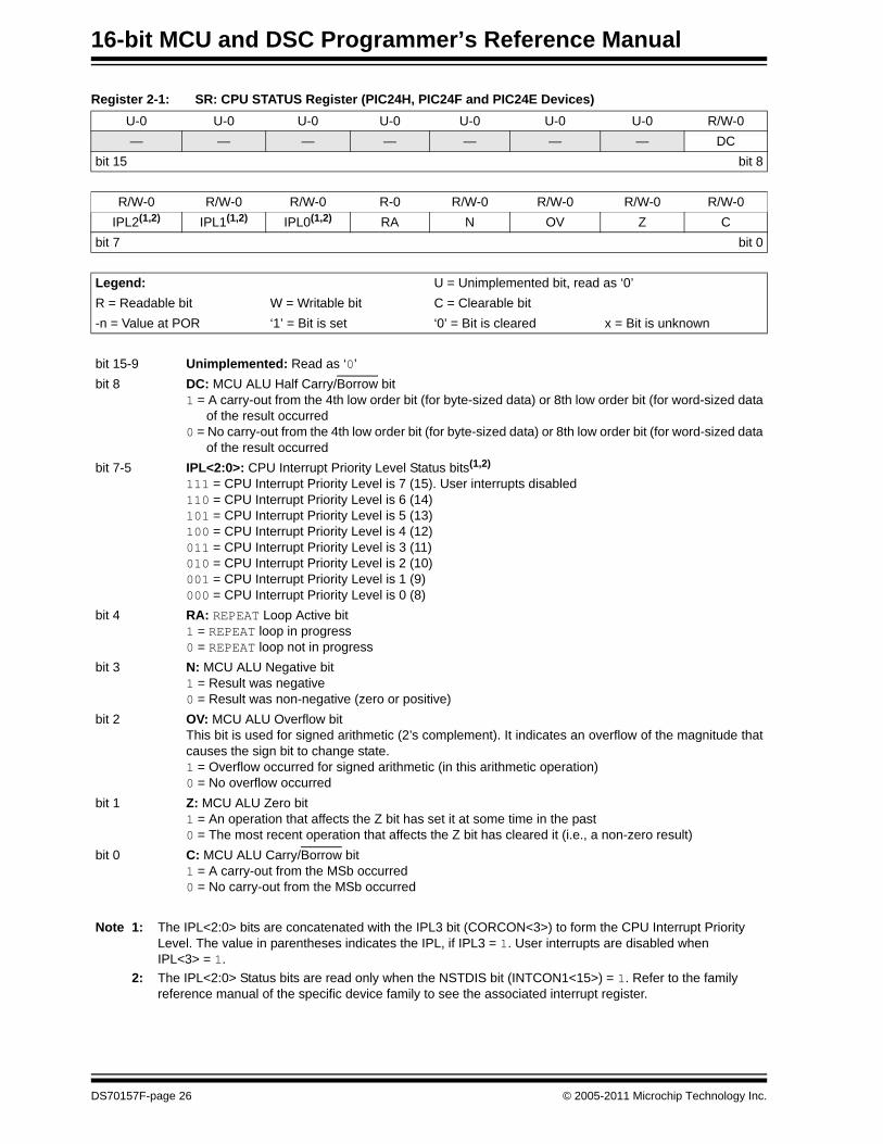
Depending on the MCU and DSC family, one of the following STATUS registers is used:
• Register 2-1 for PIC24F, PIC24H, and PIC24E devices• Register 2-2 for dsPIC30F and dsPIC33F devices• Register 2-3 for dsPIC33E devices
2.16.1 MCU ALU Status BitsThe MCU operation Status bits are either affected or used by the majority of instructions in the instruction set. Most of the logic, math, rotate/shift and bit instructions modify the MCU Status bits after execution, and the conditional Branch instructions use the state of individual Status bits to determine the flow of program execution. All conditional branch instructions are listed in Section 4.8 “Conditional Branch Instructions”.
The Carry (C), Zero (Z), Overflow (OV), Negative (N), and Digit Carry (DC) bits show the immediate status of the MCU ALU by indicating whether an operation has resulted in a Carry, Zero, Overflow, Negative result, or Digit Carry. When a subtract operation is performed, the C flag is used as a Borrow flag.
The Z Status bit is useful for extended precision arithmetic. The Z Status bit functions like a normal Z flag for all instructions except those that use a carry or borrow input (ADDC, CPB, SUBB and SUBBR). See Section 4.9 “Z Status Bit” for more detailed information.
2.16.2 REPEAT Loop Status BitThe REPEAT Active bit (RA) is used to indicate when looping is active. The RA flag indicates that a REPEAT instruction is being executed, and it is only affected by the REPEAT instructions. The RA flag is set to ‘1’ when the instruction being repeated begins execution, and it is cleared when the instruction being repeated completes execution for the last time.
Since the RA flag is also read-only, it may not be directly cleared. However, if a REPEAT or its target instruction is interrupted, the Interrupt Service Routine may clear the RA flag of the SRL, which resides on the stack. This action will disable looping once program execution returns from the Interrupt Service Routine, because the restored RA will be ‘0’.
Note 1: For dsPIC30F and dsPIC33F devices, DOEND has a shadow register. See Section 2.18 “Shadow Registers” for information on shadow registers.
2: The dsPIC33E devices have a 4-level-deep, nested DO stack instead of a shadow register.
3: Refer to the specific device family reference manual for complete details about DOloops.
Note 1: All MCU bits are shadowed during execution of the PUSH.S instruction and they are restored on execution of the POP.S instruction.
2: All MCU bits, except the DC flag (which is not in the SRL), are stacked during exception processing (see Section 4.7.1 “Software Stack Pointer”).
© 2005-2011 Microchip Technology Inc. DS70157F-page 21

16-bit MCU and DSC Programmer’s Reference Manual
2.16.3 DO Active bit (DA) (dsPIC30F, dsPIC33F and dsPIC33E Devices)The DO Active bit (DA) is used to indicate when looping is active. The DO instructions affect the DA flag, which indicates that a DO loop is active. The DA flag is set to ‘1’ when the first instruction of the DO loop is executed, and it is cleared when the last instruction of the loop completes final execution.
The DA flag is read-only. This means that looping is not initiated by writing a ‘1’ to DA, nor is it terminated by writing a ‘0’ to DA. If a DO loop must be terminated prematurely, the EDT bit, CORCON<11>, should be used.
DS70157F-page 22 © 2005-2011 Microchip Technology Inc.
Section 2. Programmer’s ModelProgram
mer’s
Model
2
2.16.4 DSP ALU Status Bits (dsPIC30F, dsPIC33F and dsPIC33E Devices)
The high byte of the STATUS Register (SRH) is used by the DSP class of instructions, and it is modified when data passes through one of the adders. The SRH provides status information about overflow and saturation for both accumulators. The Saturate A, Saturate B, Overflow A and Overflow B (SA, SB, OA, OB) bits provide individual accumulator status, while the Saturate AB and Overflow AB (SAB, OAB) bits provide combined accumulator status. The SAB and OAB bits provide an efficient method for the software developer to check the register for saturation or overflow.
The OA and OB bits are used to indicate when an operation has generated an overflow into the guard bits (bits 32 through 39) of the respective accumulator. This condition can only occur when the processor is in Super Saturation mode, or if saturation is disabled. It indicates that the operation has generated a number which cannot be represented with the lower 31 bits of the accumulator. The OA and OB bits are writable in dsPIC33E devices.
The SA and SB bits are used to indicate when an operation has generated an overflow out of the MSb of the respective accumulator. The SA and SB bits are active, regardless of the Saturation mode (Disabled, Normal or Super) and may be considered “sticky”. Namely, once the SA or SB bit is set to ‘1’, it can only be cleared manually by software, regardless of subsequent DSP operations. When it is required, the BCLR instruction can be used to clear the SA or SB bit.
In addition, the SA and SB bits can be set by software in dsPIC33E devices, enabling efficient context state switching.
For convenience, the OA and OB bits are logically ORed together to form the OAB flag, and the SA and SB bits are logically ORed to form the SAB flag. These cumulative Status bits provide efficient overflow and saturation checking when an algorithm is implemented. Instead of interrogating the OA and the OB bits independently for arithmetic overflows, a single check of OAB can be performed. Likewise, when checking for saturation, SAB may be examined instead of checking both the SA and SB bits. Note that clearing the SAB flag will clear both the SA and SB bits.
2.16.5 Interrupt Priority Level Status BitsThe three Interrupt Priority Level (IPL) bits of the SRL, SR<7:5>, and the IPL3 bit, CORCON<3>, set the CPU’s IPL which is used for exception processing. Exceptions consist of interrupts and hardware traps. Interrupts have a user-defined priority level between 0 and 7, while traps have a fixed priority level between 8 and 15. The fourth Interrupt Priority Level bit, IPL3, is a special IPL bit that may only be read or cleared by the user. This bit is only set when a hardware trap is activated and it is cleared after the trap is serviced.
The CPU’s IPL identifies the lowest level exception which may interrupt the processor. The interrupt level of a pending exception must always be greater than the CPU’s IPL for the CPU to process the exception. This means that if the IPL is 0, all exceptions at priority Level 1 and above may interrupt the processor. If the IPL is 7, only hardware traps may interrupt the processor.
When an exception is serviced, the IPL is automatically set to the priority level of the exception being serviced, which will disable all exceptions of equal and lower priority. However, since the IPL field is read/write, one may modify the lower three bits of the IPL in an Interrupt Service Routine to control which exceptions may preempt the exception processing. Since the SRL is stacked during exception processing, the original IPL is always restored after the exception is serviced. If required, one may also prevent exceptions from nesting by setting the NSTDIS bit(INTCON1<15>).
Note: For more detailed information on exception processing, refer to the family reference manual of the specific device.
© 2005-2011 Microchip Technology Inc. DS70157F-page 23

16-bit MCU and DSC Programmer’s Reference Manual
2.17 CORE CONTROL REGISTER For all MCU and DSC devices, the 16-bit CPU Core Control register (CORCON), is used to set the configuration of the CPU. This register provides the ability to map program space into data space.
In addition to setting CPU modes, the CORCON register contains status information about the IPL<3> Status bit, which indicates if a trap exception is being processed.
Depending on the MCU and DSC family, one of the following CORCON registers is used:
• Register 2-4 for PIC24F and PIC24H devices• Register 2-5 for PIC24E devices• Register 2-6 for dsPIC30F and dsPIC33F devices• Register 2-7 for dsPIC33E devices
2.17.1 dsPIC30F, dsPIC33F, and dsPIC33E Specific bitsIn addition to setting CPU modes, the following features are available through the CORCON register:
• Set the ACCA and ACCB saturation enable• Set the Data Space Write Saturation mode• Set the Accumulator Saturation and Rounding modes• Set the Multiplier mode for DSP operations• Terminate DO loops prematurely• Provide status information about the DO loop nesting level (DL<2:0>)• Select fixed or variable interrupt latency (dsPIC33E only)
2.17.1.1 PIC24E and dsPIC33E SPECIFIC BITS
A Status bit (SFA) is available that indicates whether the Stack Frame is active.
2.18 SHADOW REGISTERSA shadow register is used as a temporary holding register and can transfer its contents to or from the associated host register when instructed. Some of the registers in the programmer’s model have a shadow register, which is utilized during the execution of a DO, POP.S, or PUSH.Sinstruction. Shadow register usage is shown in Table 2-2.
For dsPIC30F and dsPIC33F devices, since the DCOUNT, DOSTART and DOEND registers are shadowed, the ability to nest DO loops without additional overhead is provided. Since all shadow registers are one register deep, up to one level of DO loop nesting is possible. Further nesting of DO loops is possible in software, with support provided by the DO Loop Nesting Level Status bits (DL<2:0>) in the CORCON register (CORCON<10:8>).
Note: PIC24E and dsPIC33E devices do not have a PSV control bit, it has been replaced by the SFA bit.
Note: The DO instruction is only available in dsPIC30F, dsPIC33F, and dsPIC33E devices.
Table 2-2: Automatic Shadow Register Usage
Location DO(1) POP.S/PUSH.S
DCOUNT(1) Yes —
DOSTART(1) Yes —
DOEND(1) Yes —
STATUS Register – DC, N, OV, Z and C bits — YesW0-W3 — YesNote 1: The DO shadow registers are only available in dsPIC30F and dsPIC33F devices.
Note: All shadow registers are one register deep and not directly accessible. Additional shadowing may be performed in software using the software stack.
DS70157F-page 24 © 2005-2011 Microchip Technology Inc.
Section 2. Programmer’s ModelProgram
mer’s
Model
2
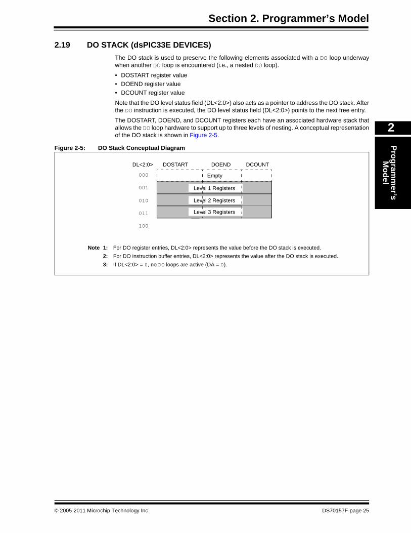
2.19 DO STACK (dsPIC33E DEVICES)The DO stack is used to preserve the following elements associated with a DO loop underway when another DO loop is encountered (i.e., a nested DO loop).
• DOSTART register value• DOEND register value• DCOUNT register value
Note that the DO level status field (DL<2:0>) also acts as a pointer to address the DO stack. After the DO instruction is executed, the DO level status field (DL<2:0>) points to the next free entry.
The DOSTART, DOEND, and DCOUNT registers each have an associated hardware stack that allows the DO loop hardware to support up to three levels of nesting. A conceptual representation of the DO stack is shown in Figure 2-5.
Figure 2-5: DO Stack Conceptual Diagram
DCOUNTDOENDDOSTARTDL<2:0>
Empty
Level 3 Registers
000
001
010
011
100
Level 2 Registers
Level 1 Registers
Note 1: For DO register entries, DL<2:0> represents the value before the DO stack is executed.2: For DO instruction buffer entries, DL<2:0> represents the value after the DO stack is executed.3: If DL<2:0> = 0, no DO loops are active (DA = 0).
© 2005-2011 Microchip Technology Inc. DS70157F-page 25
16-bit MCU and DSC Programmer’s Reference Manual
Register 2-1: SR: CPU STATUS Register (PIC24H, PIC24F and PIC24E Devices) U-0 U-0 U-0 U-0 U-0 U-0 U-0 R/W-0— — — — — — — DC
bit 15 bit 8
R/W-0 R/W-0 R/W-0 R-0 R/W-0 R/W-0 R/W-0 R/W-0IPL2(1,2) IPL1(1,2) IPL0(1,2) RA N OV Z C
bit 7 bit 0
Legend: U = Unimplemented bit, read as ‘0’R = Readable bit W = Writable bit C = Clearable bit-n = Value at POR ‘1’ = Bit is set ‘0’ = Bit is cleared x = Bit is unknown
bit 15-9 Unimplemented: Read as ‘0’bit 8 DC: MCU ALU Half Carry/Borrow bit
1 = A carry-out from the 4th low order bit (for byte-sized data) or 8th low order bit (for word-sized data of the result occurred
0 = No carry-out from the 4th low order bit (for byte-sized data) or 8th low order bit (for word-sized data of the result occurred
bit 7-5 IPL<2:0>: CPU Interrupt Priority Level Status bits(1,2)
111 = CPU Interrupt Priority Level is 7 (15). User interrupts disabled 110 = CPU Interrupt Priority Level is 6 (14)101 = CPU Interrupt Priority Level is 5 (13)100 = CPU Interrupt Priority Level is 4 (12)011 = CPU Interrupt Priority Level is 3 (11)010 = CPU Interrupt Priority Level is 2 (10)001 = CPU Interrupt Priority Level is 1 (9)000 = CPU Interrupt Priority Level is 0 (8)
bit 4 RA: REPEAT Loop Active bit1 = REPEAT loop in progress0 = REPEAT loop not in progress
bit 3 N: MCU ALU Negative bit1 = Result was negative0 = Result was non-negative (zero or positive)
bit 2 OV: MCU ALU Overflow bitThis bit is used for signed arithmetic (2’s complement). It indicates an overflow of the magnitude that causes the sign bit to change state. 1 = Overflow occurred for signed arithmetic (in this arithmetic operation)0 = No overflow occurred
bit 1 Z: MCU ALU Zero bit1 = An operation that affects the Z bit has set it at some time in the past0 = The most recent operation that affects the Z bit has cleared it (i.e., a non-zero result)
bit 0 C: MCU ALU Carry/Borrow bit1 = A carry-out from the MSb occurred0 = No carry-out from the MSb occurred
Note 1: The IPL<2:0> bits are concatenated with the IPL3 bit (CORCON<3>) to form the CPU Interrupt Priority Level. The value in parentheses indicates the IPL, if IPL3 = 1. User interrupts are disabled when IPL<3> = 1.
2: The IPL<2:0> Status bits are read only when the NSTDIS bit (INTCON1<15>) = 1. Refer to the family reference manual of the specific device family to see the associated interrupt register.
DS70157F-page 26 © 2005-2011 Microchip Technology Inc.
Section 2. Programmer’s ModelProgram
mer’s
Model
2
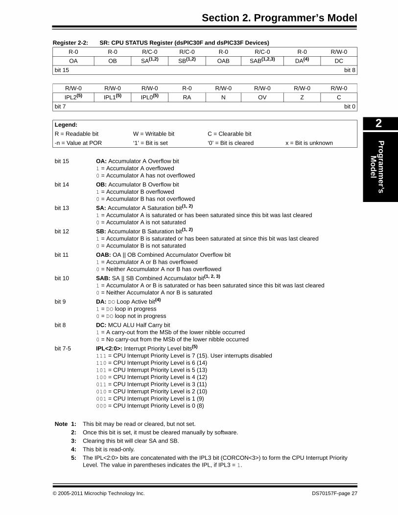
Register 2-2: SR: CPU STATUS Register (dsPIC30F and dsPIC33F Devices) R-0 R-0 R/C-0 R/C-0 R-0 R/C-0 R-0 R/W-0OA OB SA(1,2) SB(1,2) OAB SAB(1,2,3) DA(4) DC
bit 15 bit 8
R/W-0 R/W-0 R/W-0 R-0 R/W-0 R/W-0 R/W-0 R/W-0IPL2(5) IPL1(5) IPL0(5) RA N OV Z C
bit 7 bit 0
Legend:R = Readable bit W = Writable bit C = Clearable bit-n = Value at POR ‘1’ = Bit is set ‘0’ = Bit is cleared x = Bit is unknown
bit 15 OA: Accumulator A Overflow bit 1 = Accumulator A overflowed0 = Accumulator A has not overflowed
bit 14 OB: Accumulator B Overflow bit1 = Accumulator B overflowed0 = Accumulator B has not overflowed
bit 13 SA: Accumulator A Saturation bit(1, 2)
1 = Accumulator A is saturated or has been saturated since this bit was last cleared0 = Accumulator A is not saturated
bit 12 SB: Accumulator B Saturation bit(1, 2)
1 = Accumulator B is saturated or has been saturated at since this bit was last cleared0 = Accumulator B is not saturated
bit 11 OAB: OA || OB Combined Accumulator Overflow bit1 = Accumulator A or B has overflowed0 = Neither Accumulator A nor B has overflowed
bit 10 SAB: SA || SB Combined Accumulator bit(1, 2, 3)
1 = Accumulator A or B is saturated or has been saturated since this bit was last cleared0 = Neither Accumulator A nor B is saturated
bit 9 DA: DO Loop Active bit(4)
1 = DO loop in progress0 = DO loop not in progress
bit 8 DC: MCU ALU Half Carry bit1 = A carry-out from the MSb of the lower nibble occurred0 = No carry-out from the MSb of the lower nibble occurred
bit 7-5 IPL<2:0>: Interrupt Priority Level bits(5)
111 = CPU Interrupt Priority Level is 7 (15). User interrupts disabled110 = CPU Interrupt Priority Level is 6 (14)101 = CPU Interrupt Priority Level is 5 (13)100 = CPU Interrupt Priority Level is 4 (12)011 = CPU Interrupt Priority Level is 3 (11)010 = CPU Interrupt Priority Level is 2 (10)001 = CPU Interrupt Priority Level is 1 (9)000 = CPU Interrupt Priority Level is 0 (8)
Note 1: This bit may be read or cleared, but not set.2: Once this bit is set, it must be cleared manually by software.3: Clearing this bit will clear SA and SB.4: This bit is read-only.5: The IPL<2:0> bits are concatenated with the IPL3 bit (CORCON<3>) to form the CPU Interrupt Priority
Level. The value in parentheses indicates the IPL, if IPL3 = 1.
© 2005-2011 Microchip Technology Inc. DS70157F-page 27

16-bit MCU and DSC Programmer’s Reference Manual
bit 4 RA: REPEAT Loop Active bit1 = REPEAT loop in progress0 = REPEAT loop not in progress
bit 3 N: MCU ALU Negative bit1 = The result of the operation was negative0 = The result of the operation was not negative
bit 2 OV: MCU ALU Overflow bit1 = Overflow occurred0 = No overflow occurred
bit 1 Z: MCU ALU Zero bit1 = The result of the operation was zero0 = The result of the operation was not zero
bit 0 C: MCU ALU Carry/Borrow bit1 = A carry-out from the MSb occurred0 = No carry-out from the MSb occurred
Register 2-2: SR: CPU STATUS Register (dsPIC30F and dsPIC33F Devices) (Continued)
Note 1: This bit may be read or cleared, but not set.2: Once this bit is set, it must be cleared manually by software.3: Clearing this bit will clear SA and SB.4: This bit is read-only.5: The IPL<2:0> bits are concatenated with the IPL3 bit (CORCON<3>) to form the CPU Interrupt Priority
Level. The value in parentheses indicates the IPL, if IPL3 = 1.
DS70157F-page 28 © 2005-2011 Microchip Technology Inc.

Section 2. Programmer’s ModelProgram
mer’s
Model
2
Register 2-3: SR: CPU STATUS Register (dsPIC33E Devices) R/W-0 R/W-0 R/W-0 R/W-0 R/C-0 R/C-0 R -0 R/W-0
OA OB SA(3) SB(3) OAB SAB DA DCbit 15 bit 8
R/W-0 R/W-0 R/W-0 R-0 R/W-0 R/W-0 R/W-0 R/W-0IPL2(1,2) IPL1(1,2) IPL0(1,2) RA N OV Z C
bit 7 bit 0
Legend: U = Unimplemented bit, read as ‘0’R = Readable bit W = Writable bit C = Clearable bit-n = Value at POR ‘1’ = Bit is set ‘0’ = Bit is cleared x = Bit is unknown
bit 15 OA: Accumulator A Overflow Status bit1 = Accumulator A has overflowed0 = Accumulator A has not overflowed
bit 14 OB: Accumulator B Overflow Status bit1 = Accumulator B has overflowed0 = Accumulator B has not overflowed
bit 13 SA: Accumulator A Saturation Status bit1 = Accumulator A is saturated or has been saturated since this bit was last cleared0 = Accumulator A is not saturated
bit 12 SB: Accumulator B Saturation Status bit1 = Accumulator B is saturated or has been saturated since this bit was last cleared0 = Accumulator B is not saturated
bit 11 OAB: OA || OB Combined Accumulator Overflow Status bit1 = Accumulator A or B has overflowed0 = Neither Accumulator A nor B has overflowed
bit 10 SAB: SA || SB Combined Accumulator Status bit1 = Accumulator A or B is saturated or has been saturated since this bit was last cleared0 = Neither Accumulator A nor B is saturated
bit 9 DA: DO Loop Active bit1 = DO loop in progress0 = DO loop not in progress
bit 8 DC: MCU ALU Half Carry/Borrow bit1 = A carry-out from the 4th low order bit (for byte-sized data) or 8th low order bit (for word-sized data
of the result occurred0 = No carry-out from the 4th low order bit (for byte-sized data) or 8th low order bit (for word-sized data
of the result occurred
Note 1: The IPL<2:0> bits are concatenated with the IPL3 bit (CORCON<3>) to form the CPU Interrupt Priority Level. The value in parentheses indicates the IPL, if IPL3 = 1. User interrupts are disabled when IPL3 = 1.
2: The IPL<2:0> Status bits are read only when NSTDIS bit (INTCON1<15>) = 1. Refer to the family reference manual of the specific device family to see the associated interrupt register.
3: A data write to SR can modify the SA or SB bits by either a data write to SA and SB or by clearing the SAB bit. To avoid a possible SA/SB bit write race-condition, the SA and SB bits should not be modified using bit operations.
© 2005-2011 Microchip Technology Inc. DS70157F-page 29

16-bit MCU and DSC Programmer’s Reference Manual
bit 7-5 IPL<2:0>: CPU Interrupt Priority Level Status bits(1,2)
111 = CPU Interrupt Priority Level is 7 (15). User interrupts disabled 110 = CPU Interrupt Priority Level is 6 (14)101 = CPU Interrupt Priority Level is 5 (13)100 = CPU Interrupt Priority Level is 4 (12)011 = CPU Interrupt Priority Level is 3 (11)010 = CPU Interrupt Priority Level is 2 (10)001 = CPU Interrupt Priority Level is 1 (9)000 = CPU Interrupt Priority Level is 0 (8)
bit 4 RA: REPEAT Loop Active bit1 = REPEAT loop in progress0 = REPEAT loop not in progress
bit 3 N: MCU ALU Negative bit1 = Result was negative0 = Result was non-negative (zero or positive)
bit 2 OV: MCU ALU Overflow bitThis bit is used for signed arithmetic (2’s complement). It indicates an overflow of the magnitude that causes the sign bit to change state. 1 = Overflow occurred for signed arithmetic (in this arithmetic operation)0 = No overflow occurred
bit 1 Z: MCU ALU Zero bit1 = The result of the operation was zero0 = The result of the operation was not zero
bit 0 C: MCU ALU Carry/Borrow bit1 = A carry-out from the MSb of the result occurred0 = No carry-out from the MSb of the result occurred
Register 2-3: SR: CPU STATUS Register (dsPIC33E Devices) (Continued)
Note 1: The IPL<2:0> bits are concatenated with the IPL3 bit (CORCON<3>) to form the CPU Interrupt Priority Level. The value in parentheses indicates the IPL, if IPL3 = 1. User interrupts are disabled when IPL3 = 1.
2: The IPL<2:0> Status bits are read only when NSTDIS bit (INTCON1<15>) = 1. Refer to the family reference manual of the specific device family to see the associated interrupt register.
3: A data write to SR can modify the SA or SB bits by either a data write to SA and SB or by clearing the SAB bit. To avoid a possible SA/SB bit write race-condition, the SA and SB bits should not be modified using bit operations.
DS70157F-page 30 © 2005-2011 Microchip Technology Inc.

Section 2. Programmer’s ModelProgram
mer’s
Model
2
Register 2-4: CORCON: Core Control Register (PIC24F and PIC24H Devices) U-0 U-0 U-0 U-0 U-0 U-0 U-0 U-0— — — — — — — —
bit 15 bit 8
U-0 U-0 U-0 U-0 R/C-0 R/W-0 U-0 U-0— — — — IPL3(1,2) PSV — —
bit 7 bit 0
Legend: C = Clearable bit R = Readable bit W = Writable bit-n = Value at POR ‘1’ = Bit is set ‘0’ = Bit is cleared x = Bit is unknownU = Unimplemented bit, read as ‘0’
bit 15-4 Unimplemented: Read as ‘0’bit 3 IPL3: Interrupt Priority Level 3 Status bit(1,2)
1 = CPU Interrupt Priority Level is 8 or greater (trap exception activated)0 = CPU Interrupt Priority Level is 7 or less (no trap exception activated)
bit 2 PSV: Program Space Visibility in Data Space Enable bit1 = Program space visible in data space0 = Program space not visible in data space
bit 1-0 Unimplemented: Read as ‘0’
Note 1: This bit may be read or cleared, but not set.2: This bit is concatenated with the IPL<2:0> bits (SR<7:5>) to form the CPU Interrupt Priority Level.
© 2005-2011 Microchip Technology Inc. DS70157F-page 31

16-bit MCU and DSC Programmer’s Reference Manual
Register 2-5: CORCON: Core Control Register (PIC24E Devices) R/W-0 U-0 U-0 U-0 U-0 U-0 U-0 U-0VAR — — — — — — —
bit 15 bit 8
U-0 U-0 U-0 U-0 R/C-0 R-0 U-0 U-0— — — — IPL3(1,2) SFA — —
bit 7 bit 0
Legend:R = Readable bit W = Writable bit U = Unimplemented bit, read as ‘0’-n = Value at POR ‘1’ = Bit is set ‘0’ = Bit is cleared x = Bit is unknown
bit 15 VAR: Variable Exception Processing Latency Control bit1 = Variable (bounded deterministic) exception processing latency0 = Fixed (fully deterministic) exception processing latency
bit 14-4 Unimplemented: Read as '0’bit 3 IPL3: CPU Interrupt Priority Level Status bit 3(1)
1 = CPU interrupt priority level is greater than 70 = CPU interrupt priority level is 7 or less
bit 2 SFA: Stack Frame Active Status bit1 = Stack frame is active. W14 and W15 address 0x0000 to 0xFFFF, regardless of DSRPAG and
DSWPAG values.0 = Stack frame is not active. W14 and W15 address of EDS or Base Data Space
bit 1-0 Unimplemented: Read as '0’
Note 1: This bit may be read or cleared, but not set.2: The IPL3 bit is concatenated with the IPL<2:0> bits (SR<7:5>) to form the CPU interrupt priority level.
DS70157F-page 32 © 2005-2011 Microchip Technology Inc.

Section 2. Programmer’s ModelProgram
mer’s
Model
2
Register 2-6: CORCON: Core Control Register (dsPIC30F and dsPIC33F Devices) U-0 U-0 U-0 R/W-0 R(0)/W-0 R-0 R-0 R-0— — — US EDT(1) DL<2:0>(2,3)
bit 15 bit 8
R/W-0 R/W-0 R/W-1 R/W-0 R/C-0 R/W-0 R/W-0 R/W-0SATA SATB SATDW ACCSAT IPL3(4,5) PSV RND IF
bit 7 bit 0
Legend: C = Clearable bit R = Readable bit W = Writable bit-n = Value at POR ‘1’ = Bit is set ‘0’ = Bit is cleared x = Bit is unknownU = Unimplemented bit, read as ‘0’
bit 15-13 Unimplemented: Read as ‘0’bit 12 US: Unsigned or Signed Multiplier Mode Select bit
1 = Unsigned mode enabled for DSP multiply operations0 = Signed mode enabled for DSP multiply operations
bit 11 EDT: Early DO Loop Termination Control bit(1)
1 = Terminate executing DO loop at end of current iteration0 = No effect
bit 10-8 DL<2:0>: DO Loop Nesting Level Status bits(2, 3)
111 = DO looping is nested at 7 levels110 = DO looping is nested at 6 levels110 = DO looping is nested at 5 levels110 = DO looping is nested at 4 levels011 = DO looping is nested at 3 levels010 = DO looping is nested at 2 levels001 = DO looping is active, but not nested (just 1 level)000 = DO looping is not active
bit 7 SATA: ACCA Saturation Enable bit1 = Accumulator A saturation enabled0 = Accumulator A saturation disabled
bit 6 SATB: ACCB Saturation Enable bit1 = Accumulator B saturation enabled0 = Accumulator B saturation disabled
bit 5 SATDW: Data Space Write from DSP Engine Saturation Enable bit1 = Data space write saturation enabled0 = Data space write saturation disabled
bit 4 ACCSAT: Accumulator Saturation Mode Select bit1 = 9.31 saturation (Super Saturation)0 = 1.31 saturation (Normal Saturation)
bit 3 IPL3: Interrupt Priority Level 3 Status bit(4, 5)
1 = CPU Interrupt Priority Level is 8 or greater (trap exception activated)0 = CPU Interrupt Priority Level is 7 or less (no trap exception activated)
bit 2 PSV: Program Space Visibility in Data Space Enable bit1 = Program space visible in data space0 = Program space not visible in data space
Note 1: This bit will always read ‘0’.2: DL<2:1> are read-only.3: The first two levels of DO loop nesting are handled by hardware.4: This bit may be read or cleared, but not set.5: This bit is concatenated with the IPL<2:0> bits (SR<7:5>) to form the CPU Interrupt Priority Level.
© 2005-2011 Microchip Technology Inc. DS70157F-page 33

16-bit MCU and DSC Programmer’s Reference Manual
bit 1 RND: Rounding Mode Select bit1 = Biased (conventional) rounding enabled0 = Unbiased (convergent) rounding enabled
bit 0 IF: Integer or Fractional Multiplier Mode Select bit1 = Integer mode enabled for DSP multiply operations0 = Fractional mode enabled for DSP multiply operations
Register 2-6: CORCON: Core Control Register (dsPIC30F and dsPIC33F Devices) (Continued)
Note 1: This bit will always read ‘0’.2: DL<2:1> are read-only.3: The first two levels of DO loop nesting are handled by hardware.4: This bit may be read or cleared, but not set.5: This bit is concatenated with the IPL<2:0> bits (SR<7:5>) to form the CPU Interrupt Priority Level.
DS70157F-page 34 © 2005-2011 Microchip Technology Inc.

Section 2. Programmer’s ModelProgram
mer’s
Model
2
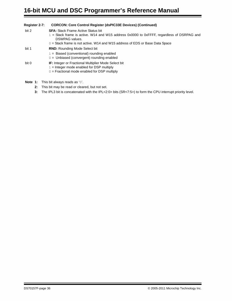
Register 2-7: CORCON: Core Control Register (dsPIC33E Devices) R/W-0 U-0 R/W-0 R/W-0 R/W-0 R-0 R-0 R-0VAR — US<1:0> EDT(1) DL<2:0>
bit 15 bit 8
R/W-0 R/W-0 R/W-1 R/W-0 R/C-0 R-0 R/W-0 R/W-0SATA SATB SATDW ACCSAT IPL3(2,3) SFA RND IF
bit 7 bit 0
Legend:R = Readable bit W = Writable bit U = Unimplemented bit, read as ‘0’-n = Value at POR ‘1’ = Bit is set ‘0’ = Bit is cleared x = Bit is unknown
bit 15 VAR: Variable Exception Processing Latency Control bit1 = Variable (bounded deterministic) exception processing latency0 = Fixed (fully deterministic) exception processing latency
bit 14 Unimplemented: Read as '0’bit 13-12 US<1:0>: DSP Multiply Unsigned/Signed Control bits
11 = Reserved10 = DSP engine multiplies are mixed-sign01 = DSP engine multiplies are unsigned 00 = DSP engine multiplies are signed
bit 11 EDT: Early DO Loop Termination Control bit(1)
1 = Terminate executing DO loop at end of current loop iteration0 = No effect
bit 10-8 DL<2:0>: DO Loop Nesting Level Status bits111 = 7 DO loops active•••001 = 1 DO loop active000 = 0 DO loops active
bit 7 SATA: ACCA Saturation Enable bit1 = Accumulator A saturation enabled0 = Accumulator A saturation disabled
bit 6 SATB: ACCB Saturation Enable bit1 = Accumulator B saturation enabled0 = Accumulator B saturation disabled
bit 5 SATDW: Data Space Write from DSP Engine Saturation Enable bit1 = Data space write saturation enabled0 = Data space write saturation disabled
bit 4 ACCSAT: Accumulator Saturation Mode Select bit1 = 9.31 saturation (super saturation)0 = 1.31 saturation (normal saturation)
bit 3 IPL3: CPU Interrupt Priority Level Status bit 3(2)
1 = CPU interrupt priority level is greater than 70 = CPU interrupt priority level is 7 or less
Note 1: This bit always reads as ‘0’.2: This bit may be read or cleared, but not set.3: The IPL3 bit is concatenated with the IPL<2:0> bits (SR<7:5>) to form the CPU interrupt priority level.
© 2005-2011 Microchip Technology Inc. DS70157F-page 35
16-bit MCU and DSC Programmer’s Reference Manual
bit 2 SFA: Stack Frame Active Status bit1 = Stack frame is active. W14 and W15 address 0x0000 to 0xFFFF, regardless of DSRPAG and
DSWPAG values.0 = Stack frame is not active. W14 and W15 address of EDS or Base Data Space
bit 1 RND: Rounding Mode Select bit1 = Biased (conventional) rounding enabled0 = Unbiased (convergent) rounding enabled
bit 0 IF: Integer or Fractional Multiplier Mode Select bit1 = Integer mode enabled for DSP multiply0 = Fractional mode enabled for DSP multiply
Register 2-7: CORCON: Core Control Register (dsPIC33E Devices) (Continued)
Note 1: This bit always reads as ‘0’.2: This bit may be read or cleared, but not set.3: The IPL3 bit is concatenated with the IPL<2:0> bits (SR<7:5>) to form the CPU interrupt priority level.
DS70157F-page 36 © 2005-2011 Microchip Technology Inc.

Section 3. Instruction Set Overview
Instruction Set O
verview
3
HIGHLIGHTSThis section of the manual contains the following major topics:
3.1 Introduction ..................................................................................................................... 383.2 Instruction Set Overview ................................................................................................. 383.3 Instruction Set Summary Tables ..................................................................................... 40
© 2005-2011 Microchip Technology Inc. DS70157F-page 37

16-bit MCU and DSC Programmer’s Reference Manual
3.1 INTRODUCTIONThe 16-bit MCU and DSC instruction set provides a broad suite of instructions that supporttraditional microcontroller applications, and a class of instructions that support math intensive applications. Since almost all of the functionality of the 8-bit PIC MCU instruction set has been maintained, this hybrid instruction set allows an easy 16-bit migration path for users already familiar with the PIC microcontroller.
3.2 INSTRUCTION SET OVERVIEWDepending on the device family, the 16-bit MCU and DSC instruction set contains up to 84 instructions, which can be grouped into the functional categories shown in Table 3-1. Table 1-2 defines the symbols used in the instruction summary tables, Table 3-2 through Table 3-11. These tables define the syntax, description, storage and execution requirements for each instruction. Storage requirements are represented in 24-bit instruction words and execution requirements are represented in instruction cycles.
Table 3-1: Instruction Groups
Most instructions have several different Addressing modes and execution flows, which require different instruction variants. For instance, depending on the device family, there are up to six unique ADD instructions and each instruction variant has its own instruction encoding. Instruction format descriptions and specific instruction operation are provided in Section 5. “Instruction Descriptions”. Additionally, a composite alphabetized instruction set table is provided in Section 7. “Reference”.
Functional Group Summary Table Page Number
Move Instructions Table 3-2 40Math Instructions Table 3-3 41Logic Instructions Table 3-4 43Rotate/Shift Instructions Table 3-5 44Bit Instructions Table 3-6 45Compare/Skip and Compare/Branch Instructions Table 3-7 46Program Flow Instructions Table 3-8 47Shadow/Stack Instructions Table 3-9 49Control Instructions Table 3-10 49DSP Instructions(1) Table 3-11 50Note 1: DSP instructions are only available in the dsPIC30F, dsPIC33F, and dsPIC33E
device families.
DS70157F-page 38 © 2005-2011 Microchip Technology Inc.

Section 3. Instruction Set OverviewInstruction Set
Overview
3
3.2.1 Multi-Cycle InstructionsAs the instruction summary tables show, most instructions execute in a single cycle, with the following exceptions:
• Instructions DO, MOV.D, POP.D, PUSH.D, TBLRDH, TBLRDL, TBLWTH and TBLWTL require 2 cycles to execute
• Instructions DIV.S, DIV.U and DIVF are single-cycle instructions, which should be executed 18 consecutive times as the target of a REPEAT instruction
• Instructions that change the program counter also require 2 cycles to execute, with the extra cycle executed as a NOP. Compare-skip instructions, which skip over a 2-word instruction, require 3 instruction cycles to execute, with 2 cycles executed as a NOP. Compare-branch instructions (dsPIC33E/PIC24E devices only) require 5 instruction cycles to execute when the branch is taken.
• The RETFIE, RETLW and RETURN are a special case of an instruction that changes the program counter. These execute in 3 cycles, unless an exception is pending and then they execute in 2 cycles.
3.2.2 Multi-Word InstructionsAs defined by Table 3-2, almost all instructions consume one instruction word (24 bits), with the exception of the CALL, DO and GOTO instructions, which are Program Flow Instructions, listed in Table 3-8. These instructions require two words of memory because their opcodes embed large literal operands.
Note: The DO and DIVF instructions are only available in the dsPIC30F, dsPIC33F, and dsPIC33E device families.
Note 1: Instructions which access program memory as data, using Program Space Visibility (PSV), will incur a one or two cycle delay for PIC24F, PIC24H, dsPIC30F, and dsPIC33F devices, whereas using PSV in dsPIC33E and PIC24E devices incurs a 4-cycle delay based on Flash memory access time. However, regardless of which device is being used, when the target instruction of a REPEAT loop accesses program memory as data, only the first execution of the target instruction is subject to the delay. See the specific device family reference manual for details.
2: All instructions may incur an additional delay on some device families, depending on Flash memory access time. For example, PIC24E and dsPIC33E devices have a 3-cycle Flash memory access time. However, instruction pipelining increases the effective instruction execution throughput. Refer to Section 2. “CPU” of the specific device family reference manual for details on instruction timing.
3: All read and read-modify-write operations (including bit operations) on non-CPU Special Function Registers (e.g., I/O Port, peripheral control, or status registers; interrupt flags, etc.) in PIC24E and dsPIC33E devices require 2 instruction cycles to execute. However, all write operations on both CPU and non-CPU Special Function Registers, and all read and read-modify-write operations on CPU Special Function Registers require 1 instruction cycle.
© 2005-2011 Microchip Technology Inc. DS70157F-page 39

16-bit MCU and DSC Programmer’s Reference Manual
3.3 INSTRUCTION SET SUMMARY TABLES
Table 3-2: Move Instructions
Assembly Syntax Description Words Cycles Page Number
EXCH Wns,Wnd Swap Wns and Wnd 1 1 243
MOV f {,WREG}(1) Move f to destination 1 1 279
MOV WREG,f Move WREG to f 1 1 280MOV f,Wnd Move f to Wnd 1 1(4) 281MOV Wns,f Move Wns to f 1 1 282MOV.B #lit8,Wnd Move 8-bit literal to Wnd 1 1 283MOV #lit16,Wnd Move 16-bit literal to Wnd 1 1 284MOV [Ws+Slit10],Wnd Move [Ws + signed 10-bit offset] to Wnd 1 1(4) 285MOV Wns,[Wd+Slit10] Move Wns to [Wd + signed 10-bit offset] 1 1 286MOV Wso,Wdo Move Wso to Wdo 1 1(4) 287MOV.D Ws,Wnd Move double Ws to Wnd:Wnd + 1 1 2(4) 289MOV.D Wns,Wd Move double Wns:Wns + 1 to Wd 1 2 289MOVPAG #lit10,DSRPAG(2) Move 10-bit literal to DSRPAG 1 1 291MOVPAG #lit9,DSWPAG(2) Move 9-bit literal to DSWPAG 1 1 291MOVPAG #lit8,TBLPAG(2) Move 8-bit literal to TBLPAG 1 1 291MOVPAG Wn, DSRPAG(2) Move Wn to DSRPAG 1 1 292MOVPAG Wn, DSWPAG(2) Move Wn to DSWPAG 1 1 292MOVPAG Wn, TBLPAG(2) Move Wn to TBLPAG 1 1 292SWAP Wn Wn = byte or nibble swap Wn 1 1 426TBLRDH [Ws],Wd Read high program word to Wd 1 2(3) 427TBLRDL [Ws],Wd Read low program word to Wd 1 2(3) 429TBLWTH Ws,[Wd] Write Ws to high program word 1 2(4) 431TBLWTL Ws,[Wd] Write Ws to low program word 1 2(4) 433Note 1: When the optional {,WREG} operand is specified, the destination of the instruction is WREG. When
{,WREG} is not specified, the destination of the instruction is the file register f.2: The MOVPAG instruction is only available in dsPIC33E and PIC24E devices.3: In dsPIC33E and PIC24E devices, these instructions require 3 additional cycles – compared to dsPIC30F,
dsPIC33F, PIC24F and PIC24H devices.4: In dsPIC33E and PIC24E devices, read and read-modify-write operations on non-CPU Special Function
Registers require an additional cycle when compared to dsPIC30F, dsPIC33F, PIC24F and PIC24H devices.
DS70157F-page 40 © 2005-2011 Microchip Technology Inc.
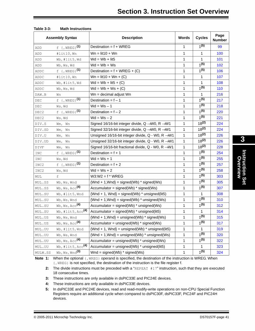
Section 3. Instruction Set OverviewInstruction Set
Overview
3
Table 3-3: Math Instructions
Assembly Syntax Description Words Cycles Page Number
ADD f {,WREG}(1) Destination = f + WREG 1 1(5) 99
ADD #lit10,Wn Wn = lit10 + Wn 1 1 100ADD Wb,#lit5,Wd Wd = Wb + lit5 1 1 101ADD Wb,Ws,Wd Wd = Wb + Ws 1 1(5) 102ADDC f {,WREG}(1) Destination = f + WREG + (C) 1 1(5) 106ADDC #lit10,Wn Wn = lit10 + Wn + (C) 1 1 107ADDC Wb,#lit5,Wd Wd = Wb + lit5 + (C) 1 1 108ADDC Wb,Ws,Wd Wd = Wb + Ws + (C) 1 1(5) 110DAW.B Wn Wn = decimal adjust Wn 1 1 216DEC f {,WREG}(1) Destination = f – 1 1 1(5) 217DEC Ws,Wd Wd = Ws – 1 1 1(5) 218DEC2 f {,WREG}(1) Destination = f – 2 1 1(5) 220DEC2 Ws,Wd Wd = Ws – 2 1 1(5) 221DIV.S Wm, Wn Signed 16/16-bit integer divide, Q → W0, R → W1 1 18(2) 224DIV.SD Wm, Wn Signed 32/16-bit integer divide, Q → W0, R → W1 1 18(2) 224DIV.U Wm, Wn Unsigned 16/16-bit integer divide, Q - W0, R → W1 1 18(2) 226DIV.UD Wm, Wn Unsigned 32/16-bit integer divide, Q - W0, R → W1 1 18(2) 226DIVF Wm, Wn Signed 16/16-bit fractional divide, Q - W0, R → W1 1 18(2) 228INC f {,WREG}(1) Destination = f + 1 1 1(5) 254INC Ws,Wd Wd = Ws + 1 1 1(5) 255INC2 f {,WREG}(1) Destination = f + 2 1 1(5) 257INC2 Ws,Wd Wd = Ws + 2 1 1(5) 258MUL f W3:W2 = f * WREG 1 1(5) 303MUL.SS Wb,Ws,Wnd {Wnd + 1,Wnd} = signed(Wb) * signed(Ws) 1 1(5) 305MUL.SS Wb,Ws,Acc(4) Accumulator = signed(Wb) * signed(Ws) 1 1(5) 307MUL.SU Wb,#lit5,Wnd {Wnd + 1, Wnd} = signed(Wb) * unsigned(lit5) 1 1 308MUL.SU Wb,Ws,Wnd {Wnd + 1,Wnd} = signed(Wb) * unsigned(Ws) 1 1(5) 310MUL.SU Wb,Ws,Acc(4) Accumulator = signed(Wb) * unsigned(Ws) 1 1(5) 312MUL.SU Wb,#lit5,Acc(4) Accumulator = signed(Wb) * unsigned(lit5) 1 1 314MUL.US Wb,Ws,Wnd {Wnd + 1,Wnd} = unsigned(Wb) * signed(Ws) 1 1(5) 315MUL.US Wb,Ws,Acc(4) Accumulator = unsigned(Wb) * signed(Ws) 1 1(5) 317MUL.UU Wb,#lit5,Wnd {Wnd + 1, Wnd} = unsigned(Wb) * unsigned(lit5) 1 1 319MUL.UU Wb,Ws,Wnd {Wnd + 1,Wnd} = unsigned(Wb) * unsigned(Ws) 1 1(5) 320MUL.UU Wb,Ws,Acc(4) Accumulator = unsigned(Wb) * unsigned(Ws) 1 1(5) 322MUL.UU Wb,#lit5,Acc(4) Accumulator = unsigned(Wb) * unsigned(lit5) 1 1 323MULW.SS Wb,Ws,Wnd(3) Wnd = signed(Wb) * signed(Ws) 1 1(5) 324Note 1: When the optional {,WREG} operand is specified, the destination of the instruction is WREG. When
{,WREG} is not specified, the destination of the instruction is the file register f.2: The divide instructions must be preceded with a “REPEAT #17” instruction, such that they are executed
18 consecutive times.3: These instructions are only available in dsPIC33E and PIC24E devices.4: These instructions are only available in dsPIC33E devices.5: In dsPIC33E and PIC24E devices, read and read-modify-write operations on non-CPU Special Function
Registers require an additional cycle when compared to dsPIC30F, dsPIC33F, PIC24F and PIC24H devices.
© 2005-2011 Microchip Technology Inc. DS70157F-page 41

16-bit MCU and DSC Programmer’s Reference Manual
MULW.SU Wb,Ws,Wnd(3) Wnd = signed(Wb) * unsigned(Ws) 1 1(5) 326MULW.SU Wb,#lit5,Wnd(3) Wnd = signed(Wb) * unsigned(lit5) 1 1 328MULW.US Wb,Ws,Wnd(3) Wnd = unsigned(Wb) * signed(Ws) 1 1(5) 329MULW.UU Wb,Ws,Wnd(3) Wnd = unsigned(Wb) * unsigned(Ws) 1 1(5) 331MULW.UU Wb,#lit5,Wnd(3) Wnd = unsigned(Wb) * unsigned(lit5) 1 1 332SE Ws,Wnd Wnd = signed-extended Ws 1 1(5) 393SUB f {,WREG}(1) Destination = f – WREG 1 1(5) 405SUB #lit10,Wn Wn = Wn – lit10 1 1 406SUB Wb,#lit5,Wd Wd = Wb – lit5 1 1 407SUB Wb,Ws,Wd Wd = Wb – Ws 1 1(5) 408
SUBB f {,WREG}(1) Destination = f – WREG – (C) 1 1(5) 411
SUBB #lit10,Wn Wn = Wn – lit10 – (C) 1 1 412
SUBB Wb,#lit5,Wd Wd = Wb – lit5 – (C) 1 1 413
SUBB Wb,Ws,Wd Wd = Wb – Ws – (C) 1 1(5) 415
SUBBR f {,WREG}(1) Destination = WREG – f – (C) 1 1(5) 417
SUBBR Wb,#lit5,Wd Wd = lit5 – Wb – (C) 1 1 418
SUBBR Wb,Ws,Wd Wd = Ws – Wb – (C) 1 1(5) 420SUBR f {,WREG}(1) Destination = WREG – f 1 1(5) 422SUBR Wb,#lit5,Wd Wd = lit5 – Wb 1 1 423SUBR Wb,Ws,Wd Wd = Ws – Wb 1 1(5) 424ZE Ws,Wnd Wnd = zero-extended Ws 1 1(5) 442
Table 3-3: Math Instructions (Continued)
Assembly Syntax Description Words Cycles Page Number
Note 1: When the optional {,WREG} operand is specified, the destination of the instruction is WREG. When {,WREG} is not specified, the destination of the instruction is the file register f.
2: The divide instructions must be preceded with a “REPEAT #17” instruction, such that they are executed 18 consecutive times.
3: These instructions are only available in dsPIC33E and PIC24E devices.4: These instructions are only available in dsPIC33E devices.5: In dsPIC33E and PIC24E devices, read and read-modify-write operations on non-CPU Special Function
Registers require an additional cycle when compared to dsPIC30F, dsPIC33F, PIC24F and PIC24H devices.
DS70157F-page 42 © 2005-2011 Microchip Technology Inc.
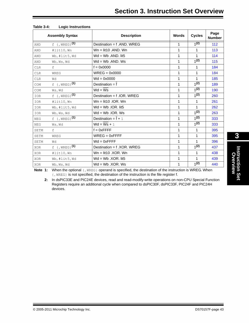
Section 3. Instruction Set OverviewInstruction Set
Overview
3
Table 3-4: Logic Instructions
Assembly Syntax Description Words Cycles Page Number
AND f {,WREG}(1) Destination = f .AND. WREG 1 1(2) 112AND #lit10,Wn Wn = lit10 .AND. Wn 1 1 113AND Wb,#lit5,Wd Wd = Wb .AND. lit5 1 1 114AND Wb,Ws,Wd Wd = Wb .AND. Ws 1 1(2) 115CLR f f = 0x0000 1 1 184CLR WREG WREG = 0x0000 1 1 184CLR Wd Wd = 0x0000 1 1 185COM f {,WREG}(1) Destination = f 1 1(2) 189COM Ws,Wd Wd = Ws 1 1(2) 190IOR f {,WREG}(1) Destination = f .IOR. WREG 1 1(2) 260IOR #lit10,Wn Wn = lit10 .IOR. Wn 1 1 261IOR Wb,#lit5,Wd Wd = Wb .IOR. lit5 1 1 262IOR Wb,Ws,Wd Wd = Wb .IOR. Ws 1 1(2) 263NEG f {,WREG}(1) Destination = f + 1 1 1(2) 333NEG Ws,Wd Wd = Ws + 1 1 1(2) 333SETM f f = 0xFFFF 1 1 395SETM WREG WREG = 0xFFFF 1 1 395SETM Wd Wd = 0xFFFF 1 1 396XOR f {,WREG}(1) Destination = f .XOR. WREG 1 1(2) 437XOR #lit10,Wn Wn = lit10 .XOR. Wn 1 1 438XOR Wb,#lit5,Wd Wd = Wb .XOR. lit5 1 1 439XOR Wb,Ws,Wd Wd = Wb .XOR. Ws 1 1(2) 440Note 1: When the optional {,WREG} operand is specified, the destination of the instruction is WREG. When
{,WREG} is not specified, the destination of the instruction is the file register f.2: In dsPIC33E and PIC24E devices, read and read-modify-write operations on non-CPU Special Function
Registers require an additional cycle when compared to dsPIC30F, dsPIC33F, PIC24F and PIC24H devices.
© 2005-2011 Microchip Technology Inc. DS70157F-page 43

16-bit MCU and DSC Programmer’s Reference Manual
Table 3-5: Rotate/Shift Instructions
Assembly Syntax Description Words Cycles Page Number
ASR f {,WREG}(1) Destination = arithmetic right shift f, LSb → C 1 1(2) 117ASR Ws,Wd Wd = arithmetic right shift Ws, LSb → C 1 1(2) 119ASR Wb,#lit4,Wnd Wnd = arithmetic right shift Wb by lit4, LSb → C 1 1 121ASR Wb,Wns,Wnd Wnd = arithmetic right shift Wb by Wns,
LSb → C1 1 122
LSR f {,WREG}(1) Destination = logical right shift f, LSb → C 1 1(2) 269LSR Ws,Wd Wd = logical right shift Ws, LSb → C 1 1(2) 271LSR Wb,#lit4,Wnd Wnd = logical right shift Wb by lit4, LSb → C 1 1 273LSR Wb,Wns,Wnd Wnd = logical right shift Wb by Wns, LSb → C 1 1 274RLC f {,WREG}(1) Destination = rotate left through Carry f 1 1(2) 373RLC Ws,Wd Wd = rotate left through Carry Ws 1 1(2) 375RLNC f {,WREG}(1) Destination = rotate left (no Carry) f 1 1(2) 377RLNC Ws,Wd Wd = rotate left (no Carry) Ws 1 1(2) 379RRC f {,WREG}(1) Destination = rotate right through Carry f 1 1(2) 381RRC Ws,Wd Wd = rotate right through Carry Ws 1 1(2) 383RRNC f {,WREG}(1) Destination = rotate right (no Carry) f 1 1(2) 385RRNC Ws,Wd Wd = rotate right (no Carry) Ws 1 1(2) 387SL f {,WREG}(1) Destination = left shift f, MSb → C 1 1(2) 399SL Ws,Wd Wd = left shift Ws, MSb → C 1 1(2) 401SL Wb,#lit4,Wnd Wnd = left shift Wb by lit4, MSb → C 1 1 403SL Wb,Wns,Wnd Wnd = left shift Wb by Wns, MSb → C 1 1 404Note 1: When the optional {,WREG} operand is specified, the destination of the instruction is WREG. When
{,WREG} is not specified, the destination of the instruction is the file register f.2: In dsPIC33E and PIC24E devices, read and read-modify-write operations on non-CPU Special Function
Registers require an additional cycle when compared to dsPIC30F, dsPIC33F, PIC24F and PIC24H devices.
DS70157F-page 44 © 2005-2011 Microchip Technology Inc.

Section 3. Instruction Set OverviewInstruction Set
Overview
3
Table 3-6: Bit Instructions
Assembly Syntax Description Words Cycles(1) Page Number
BCLR f,#bit4 Bit clear f 1 1 123BCLR Ws,#bit4 Bit clear Ws 1 1 124BSET f,#bit4 Bit set f 1 1 152BSET Ws,#bit4 Bit set Ws 1 1 153BSW.C Ws,Wb Write C bit to Ws<Wb> 1 1 155BSW.Z Ws,Wb Write Z bit to Ws<Wb> 1 1 155BTG f,#bit4 Bit toggle f 1 1 157BTG Ws,#bit4 Bit toggle Ws 1 1 158BTST f,#bit4 Bit test f to Z 1 1 168BTST.C Ws,#bit4 Bit test Ws to C 1 1 169BTST.Z Ws,#bit4 Bit test Ws to Z 1 1 169BTST.C Ws,Wb Bit test Ws<Wb> to C 1 1 171BTST.Z Ws,Wb Bit test Ws<Wb> to Z 1 1 171 BTSTS f,#bit4 Bit test f to Z, then set f 1 1 173BTSTS.C Ws,#bit4 Bit test Ws to C then set Ws 1 1 175BTSTS.Z Ws,#bit4 Bit test Ws to Z then set Ws 1 1 175FBCL Ws,Wnd Find bit change from left (MSb) side 1 1 244FF1L Ws,Wnd Find first one from left (MSb) side 1 1 246FF1R Ws,Wnd Find first one from right (LSb) side 1 1 248Note 1: In dsPIC33E and PIC24E devices, read and read-modify-write operations on non-CPU Special Function
Registers require an additional cycle when compared to dsPIC30F, dsPIC33F, PIC24F and PIC24H devices.
© 2005-2011 Microchip Technology Inc. DS70157F-page 45

16-bit MCU and DSC Programmer’s Reference Manual
Table 3-7: Compare/Skip and Compare/Branch Instructions
Assembly Syntax Description Words Cycles(1) Page Number
BTSC f,#bit4 Bit test f, skip if clear 1 1 (2 or 3)(5) 160BTSC Ws,#bit4 Bit test Ws, skip if clear 1 1 (2 or 3)(5) 162BTSS f,#bit4 Bit test f, skip if set 1 1 (2 or 3)(5) 164BTSS Ws,#bit4 Bit test Ws, skip if set 1 1 (2 or 3)(5) 166CP f Compare (f – WREG) 1 1(5) 191CP Wb,#lit5(2) Compare (Wb – lit5) 1 1 192CP Wb,#lit8(3) Compare (Wb – lit8) 1 1 193CP Wb,Ws Compare (Wb – Ws) 1 1(5) 194CP0 f Compare (f – 0x0000) 1 1(5) 196CP0 Ws Compare (Ws – 0x0000) 1 1(5) 197
CPB f Compare with Borrow (f – WREG – C) 1 1(5) 198
CPB Wb,#lit5(2) Compare with Borrow (Wb – lit5 – C) 1 1 199
CPB Wb,#lit8(3) Compare with Borrow (Wb – lit8 – C) 1 1 200
CPB Wb,Ws Compare with Borrow (Wb – Ws – C) 1 1(5) 201
CPBEQ Wb,Wn,Expr(3) Compare Wb with Wn, branch if = 1 1 (5)(4) 203
CPBGT Wb,Wn,Expr(3) Signed compare Wb with Wn, branch if > 1 1 (5)(4) 204
CPBLT Wb,Wn,Expr(3) Signed compare Wb with Wn, branch if < 1 1 (5)(4) 205
CPBNE Wb,Wn,Expr(3) Compare Wb with Wn, branch if ≠ 1 1 (5)(4) 204CPSEQ Wb, Wn Compare (Wb – Wn), skip if = 1 1 (2 or 3) 207CPSGT Wb, Wn Signed compare (Wb – Wn), skip if > 1 1 (2 or 3) 211CPSLT Wb, Wn Signed compare (Wb – Wn), skip if < 1 1 (2 or 3) 212CPSNE Wb, Wn Compare (Wb – Wn), skip if ≠ 1 1 (2 or 3) 214Note 1: Conditional skip instructions execute in 1 cycle if the skip is not taken, 2 cycles if the skip is taken over a
one-word instruction and 3 cycles if the skip is taken over a two-word instruction.2: This instruction is only available in PIC24F, PIC24H, dsPIC30F, and dsPIC33F devices.3: This instruction is only available in dsPIC33E and PIC24E devices.4: Compare-branch instructions in dsPIC33E/PIC24E devices execute in 1 cycle if the branch is not taken
and 5 cycles if the branch is taken.5: In dsPIC33E and PIC24E devices, read and read-modify-write operations on non-CPU Special Function
Registers require an additional cycle when compared to dsPIC30F, dsPIC33F, PIC24F and PIC24H devices.
DS70157F-page 46 © 2005-2011 Microchip Technology Inc.
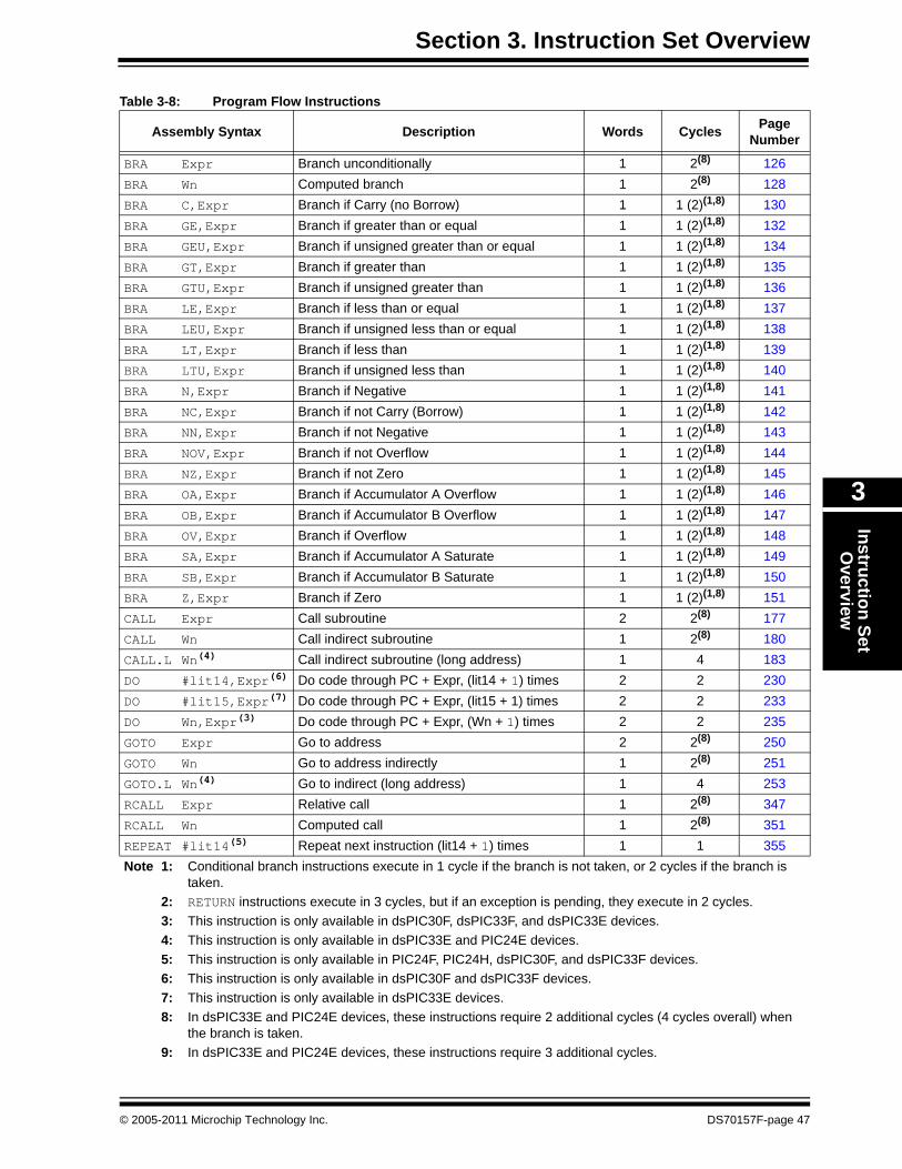
Section 3. Instruction Set OverviewInstruction Set
Overview
3
Table 3-8: Program Flow Instructions
Assembly Syntax Description Words Cycles Page Number
BRA Expr Branch unconditionally 1 2(8) 126BRA Wn Computed branch 1 2(8) 128BRA C,Expr Branch if Carry (no Borrow) 1 1 (2)(1,8) 130BRA GE,Expr Branch if greater than or equal 1 1 (2)(1,8) 132BRA GEU,Expr Branch if unsigned greater than or equal 1 1 (2)(1,8) 134BRA GT,Expr Branch if greater than 1 1 (2)(1,8) 135BRA GTU,Expr Branch if unsigned greater than 1 1 (2)(1,8) 136BRA LE,Expr Branch if less than or equal 1 1 (2)(1,8) 137BRA LEU,Expr Branch if unsigned less than or equal 1 1 (2)(1,8) 138BRA LT,Expr Branch if less than 1 1 (2)(1,8) 139BRA LTU,Expr Branch if unsigned less than 1 1 (2)(1,8) 140BRA N,Expr Branch if Negative 1 1 (2)(1,8) 141BRA NC,Expr Branch if not Carry (Borrow) 1 1 (2)(1,8) 142BRA NN,Expr Branch if not Negative 1 1 (2)(1,8) 143BRA NOV,Expr Branch if not Overflow 1 1 (2)(1,8) 144BRA NZ,Expr Branch if not Zero 1 1 (2)(1,8) 145BRA OA,Expr Branch if Accumulator A Overflow 1 1 (2)(1,8) 146BRA OB,Expr Branch if Accumulator B Overflow 1 1 (2)(1,8) 147BRA OV,Expr Branch if Overflow 1 1 (2)(1,8) 148BRA SA,Expr Branch if Accumulator A Saturate 1 1 (2)(1,8) 149BRA SB,Expr Branch if Accumulator B Saturate 1 1 (2)(1,8) 150BRA Z,Expr Branch if Zero 1 1 (2)(1,8) 151CALL Expr Call subroutine 2 2(8) 177CALL Wn Call indirect subroutine 1 2(8) 180CALL.L Wn(4) Call indirect subroutine (long address) 1 4 183DO #lit14,Expr(6) Do code through PC + Expr, (lit14 + 1) times 2 2 230DO #lit15,Expr(7) Do code through PC + Expr, (lit15 + 1) times 2 2 233DO Wn,Expr(3) Do code through PC + Expr, (Wn + 1) times 2 2 235GOTO Expr Go to address 2 2(8) 250GOTO Wn Go to address indirectly 1 2(8) 251GOTO.L Wn(4) Go to indirect (long address) 1 4 253RCALL Expr Relative call 1 2(8) 347RCALL Wn Computed call 1 2(8) 351REPEAT #lit14(5) Repeat next instruction (lit14 + 1) times 1 1 355Note 1: Conditional branch instructions execute in 1 cycle if the branch is not taken, or 2 cycles if the branch is
taken. 2: RETURN instructions execute in 3 cycles, but if an exception is pending, they execute in 2 cycles.3: This instruction is only available in dsPIC30F, dsPIC33F, and dsPIC33E devices.4: This instruction is only available in dsPIC33E and PIC24E devices.5: This instruction is only available in PIC24F, PIC24H, dsPIC30F, and dsPIC33F devices.6: This instruction is only available in dsPIC30F and dsPIC33F devices.7: This instruction is only available in dsPIC33E devices.8: In dsPIC33E and PIC24E devices, these instructions require 2 additional cycles (4 cycles overall) when
the branch is taken.9: In dsPIC33E and PIC24E devices, these instructions require 3 additional cycles.
© 2005-2011 Microchip Technology Inc. DS70157F-page 47
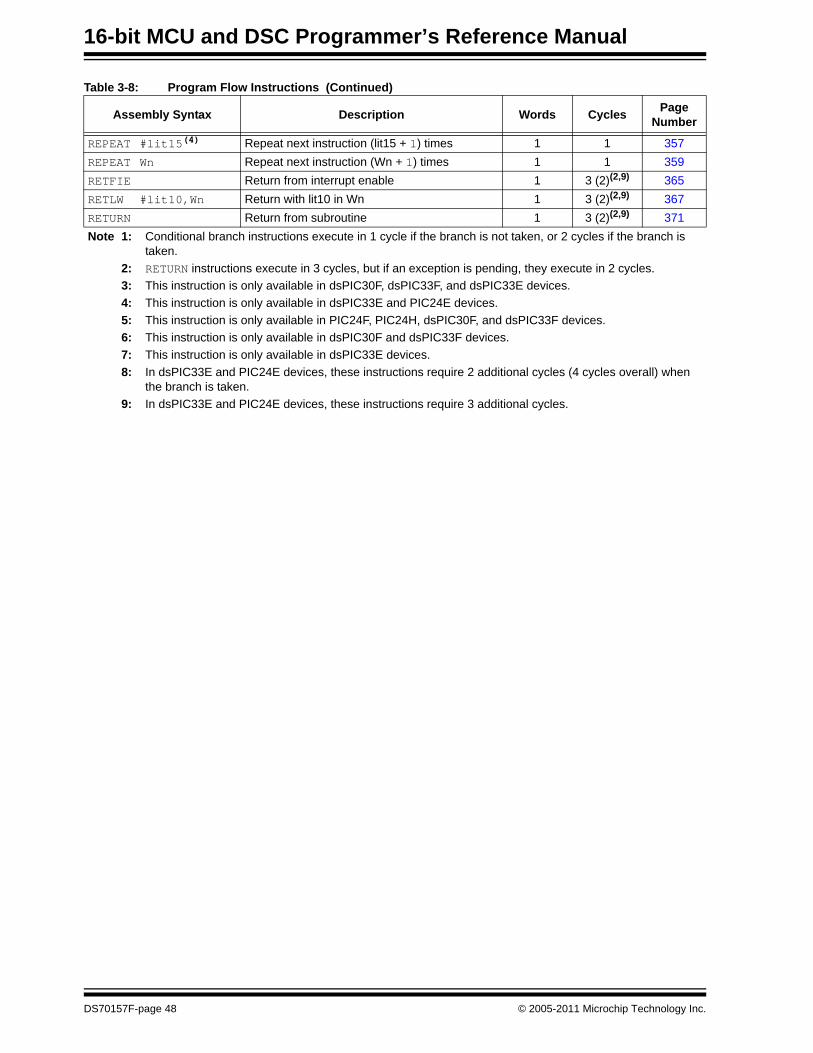
16-bit MCU and DSC Programmer’s Reference Manual
REPEAT #lit15(4) Repeat next instruction (lit15 + 1) times 1 1 357REPEAT Wn Repeat next instruction (Wn + 1) times 1 1 359RETFIE Return from interrupt enable 1 3 (2)(2,9) 365RETLW #lit10,Wn Return with lit10 in Wn 1 3 (2)(2,9) 367RETURN Return from subroutine 1 3 (2)(2,9) 371
Table 3-8: Program Flow Instructions (Continued)
Assembly Syntax Description Words Cycles Page Number
Note 1: Conditional branch instructions execute in 1 cycle if the branch is not taken, or 2 cycles if the branch is taken.
2: RETURN instructions execute in 3 cycles, but if an exception is pending, they execute in 2 cycles.3: This instruction is only available in dsPIC30F, dsPIC33F, and dsPIC33E devices.4: This instruction is only available in dsPIC33E and PIC24E devices.5: This instruction is only available in PIC24F, PIC24H, dsPIC30F, and dsPIC33F devices.6: This instruction is only available in dsPIC30F and dsPIC33F devices.7: This instruction is only available in dsPIC33E devices.8: In dsPIC33E and PIC24E devices, these instructions require 2 additional cycles (4 cycles overall) when
the branch is taken.9: In dsPIC33E and PIC24E devices, these instructions require 3 additional cycles.
DS70157F-page 48 © 2005-2011 Microchip Technology Inc.

Section 3. Instruction Set OverviewInstruction Set
Overview
3
Table 3-9: Shadow/Stack Instructions
Table 3-10: Control Instructions
Assembly Syntax Description Words Cycles Page Number
LNK #lit14 Link Frame Pointer 1 1 267POP f POP TOS to f 1 1 337POP Wdo POP TOS to Wdo 1 1 338POP.D Wnd Double POP from TOS to Wnd:Wnd + 1 1 2 339POP.S POP shadow registers 1 1 340PUSH f PUSH f to TOS 1 1(1) 341PUSH Wso PUSH Wso to TOS 1 1(1) 342PUSH.D Wns PUSH double Wns:Wns + 1 to TOS 1 2 343PUSH.S PUSH shadow registers 1 1 345ULNK Unlink Frame Pointer 1 1 435Note 1: In dsPIC33E and PIC24E devices, read and read-modify-write operations on non-CPU Special Function
Registers require an additional cycle when compared to dsPIC30F, dsPIC33F, PIC24F and PIC24H devices.
Assembly Syntax Description Words Cycles Page Number
CLRWDT Clear Watchdog Timer 1 1 188DISI #lit14 Disable interrupts for (lit14 + 1) instruction cycles 1 1 223NOP No operation 1 1 336NOPR No operation 1 1 336PWRSAV #lit1 Enter Power-saving mode lit1 1 1 346RESET Software device Reset 1 1 363
© 2005-2011 Microchip Technology Inc. DS70157F-page 49

16-bit MCU and DSC Programmer’s Reference Manual
Table 3-11: DSP Instructions (dsPIC30F, dsPIC33F and dsPIC33E Devices)
Assembly Syntax Description Words Cycles Page Number
ADD Acc Add accumulators 1 1 103ADD Wso,#Slit4,Acc 16-bit signed add to Acc 1 1(1) 104CLR Acc,[Wx],Wxd,[Wy],Wyd,AWB Clear Acc 1 1 186ED Wm*Wm,Acc,[Wx],[Wy],Wxd Euclidean distance
(no accumulate)1 1 239
EDAC Wm*Wm,Acc,[Wx],[Wy],Wxd Euclidean distance 1 1 241LAC Wso,#Slit4,Acc Load Acc 1 1(1) 265MAC Wm*Wn,Acc,[Wx],Wxd,[Wy],Wyd,AWB Multiply and accumulate 1 1 275MAC Wm*Wm,Acc,[Wx],Wxd,[Wy],Wyd Square and accumulate 1 1 277MOVSAC Acc,[Wx],Wxd,[Wy],Wyd,AWB Move Wx to Wxd and Wy to Wyd 1 1 293MPY Wm*Wn,Acc,[Wx],Wxd,[Wy],Wyd Multiply Wn by Wm to Acc 1 1 295MPY Wm*Wm,Acc,[Wx],Wxd,[Wy],Wyd Square to Acc 1 1 297MPY.N Wm*Wn,Acc,[Wx],Wxd,[Wy],Wyd -(Multiply Wn by Wm) to Acc 1 1 299MSC Wm*Wn,Acc,[Wx],Wxd,[Wy],Wyd,AWB Multiply and subtract from Acc 1 1 301NEG Acc Negate Acc 1 1 335SAC Acc,#Slit4,Wdo Store Acc 1 1 389SAC.R Acc,#Slit4,Wdo Store rounded Acc 1 1 391SFTAC Acc,#Slit6 Arithmetic shift Acc by Slit6 1 1 397SFTAC Acc,Wn Arithmetic shift Acc by (Wn) 1 1 398SUB Acc Subtract accumulators 1 1 410Note 1: In dsPIC33E and PIC24E devices, read and read-modify-write operations on non-CPU Special Function
Registers require an additional cycle when compared to dsPIC30F, dsPIC33F, PIC24F and PIC24H devices.
DS70157F-page 50 © 2005-2011 Microchip Technology Inc.

Section 4. Instruction Set Details
Instruction Set D
etails
4
HIGHLIGHTSThis section of the manual contains the following major topics:
4.1 Data Addressing Modes.................................................................................................. 524.2 Program Addressing Modes ........................................................................................... 614.3 Instruction Stalls.............................................................................................................. 624.4 Byte Operations .............................................................................................................. 644.5 Word Move Operations ................................................................................................... 664.6 Using 10-bit Literal Operands ......................................................................................... 694.7 Software Stack Pointer and Frame Pointer ..................................................................... 704.8 Conditional Branch Instructions ...................................................................................... 764.9 Z Status Bit...................................................................................................................... 774.10 Assigned Working Register Usage ................................................................................. 784.11 DSP Data Formats (dsPIC30F, dsPIC33F and dsPIC33E Devices) ............................... 814.12 Accumulator Usage (dsPIC30F, dsPIC33F and dsPIC33E Devices).............................. 834.13 Accumulator Access (dsPIC30F, dsPIC33F and dsPIC33E Devices) ............................ 844.14 DSP MAC Instructions (dsPIC30F, dsPIC33F and dsPIC33E Devices) ......................... 844.15 DSP Accumulator Instructions (dsPIC30F, dsPIC33F and dsPIC33E Devices) ............. 884.16 Scaling Data with the FBCL Instruction (dsPIC30F, dsPIC33F and dsPIC33E Devices) 884.17 Normalizing the Accumulator with the FBCL Instruction (dsPIC30F, dsPIC33F and
dsPIC33E Devices)......................................................................................................... 90
© 2005-2011 Microchip Technology Inc. DS70157F-page 51
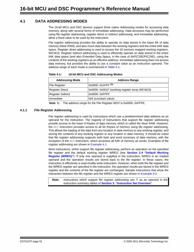
16-bit MCU and DSC Programmer’s Reference Manual
4.1 DATA ADDRESSING MODESThe 16-bit MCU and DSC devices support three native Addressing modes for accessing data memory, along with several forms of immediate addressing. Data accesses may be performed using file register addressing, register direct or indirect addressing, and immediate addressing, allow a fixed value to be used by the instruction.
File register addressing provides the ability to operate on data stored in the lower 8K of data memory (Near RAM), and also move data between the working registers and the entire 64K data space. Register direct addressing is used to access the 16 memory mapped working registers, W0:W15. Register indirect addressing is used to efficiently operate on data stored in the entire 64K data space (and also Extended Data Space, in the case of dsPIC33E/PIC24E), using the contents of the working registers as an effective address. Immediate addressing does not access data memory, but provides the ability to use a constant value as an instruction operand. The address range of each mode is summarized in Table 4-1.
Table 4-1: 16-bit MCU and DSC Addressing Modes
4.1.1 File Register Addressing
File register addressing is used by instructions which use a predetermined data address as an operand for the instruction. The majority of instructions that support file register addressing provide access to the lower 8 Kbytes of data memory, which is called the Near RAM. However, the MOV instruction provides access to all 64 Kbytes of memory using file register addressing. This allows the loading of the data from any location in data memory to any working register, and storing the contents of any working register to any location in data memory. It should be noted that file register addressing supports both byte and word accesses of data memory, with the exception of the MOV instruction, which accesses all 64K of memory as words. Examples of file register addressing are shown in Example 4-1.
Most instructions, which support file register addressing, perform an operation on the specified file register and the default working register WREG (see Section 2.4 “Default Working Register (WREG)”). If only one operand is supplied in the instruction, WREG is an implied operand and the operation results are stored back to the file register. In these cases, the instruction is effectively a read-modify-write instruction. However, when both the file register and the WREG register are specified in the instruction, the operation results are stored in the WREG register and the contents of the file register are unchanged. Sample instructions that show the interaction between the file register and the WREG register are shown in Example 4-2.
Addressing Mode Address Range
File Register 0x0000-0x1FFF (1)
Register Direct 0x0000-0x001F (working register array W0:W15)Register Indirect 0x0000-0xFFFFImmediate N/A (constant value)Note 1: The address range for the File Register MOV is 0x0000-0xFFFE.
Note: Instructions which support file register addressing use ‘f’ as an operand in the instruction summary tables of Section 3. “Instruction Set Overview”.
DS70157F-page 52 © 2005-2011 Microchip Technology Inc.
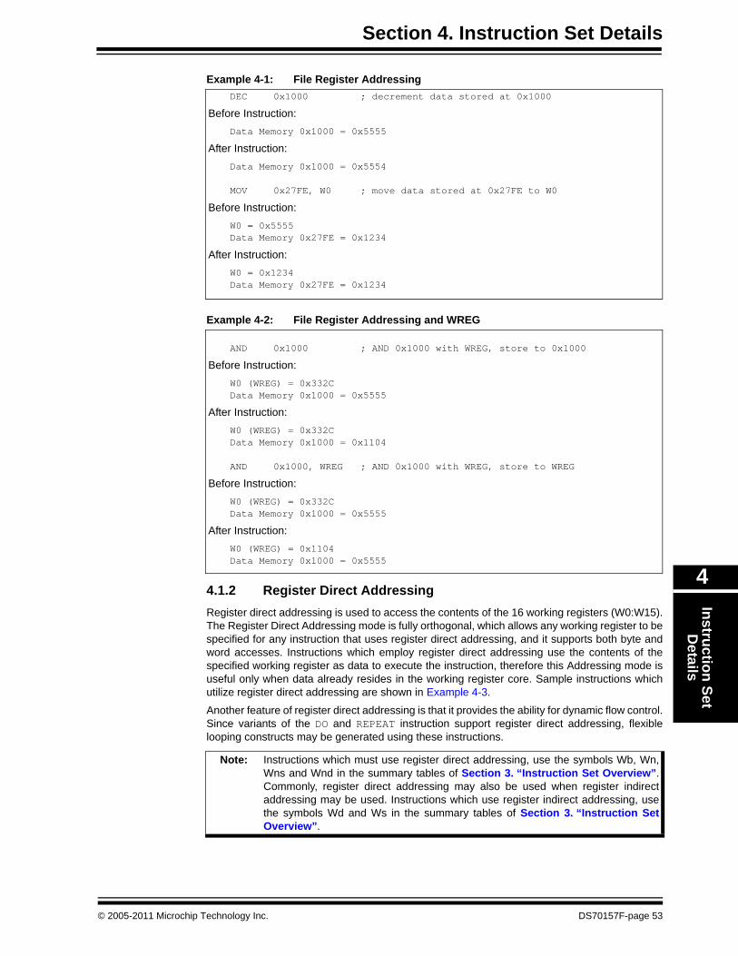
Section 4. Instruction Set DetailsInstruction Set
Details
4
Example 4-1: File Register Addressing
Example 4-2: File Register Addressing and WREG
4.1.2 Register Direct AddressingRegister direct addressing is used to access the contents of the 16 working registers (W0:W15). The Register Direct Addressing mode is fully orthogonal, which allows any working register to be specified for any instruction that uses register direct addressing, and it supports both byte and word accesses. Instructions which employ register direct addressing use the contents of the specified working register as data to execute the instruction, therefore this Addressing mode is useful only when data already resides in the working register core. Sample instructions which utilize register direct addressing are shown in Example 4-3.
Another feature of register direct addressing is that it provides the ability for dynamic flow control. Since variants of the DO and REPEAT instruction support register direct addressing, flexible looping constructs may be generated using these instructions.
DEC 0x1000 ; decrement data stored at 0x1000
Before Instruction:Data Memory 0x1000 = 0x5555
After Instruction:Data Memory 0x1000 = 0x5554
MOV 0x27FE, W0 ; move data stored at 0x27FE to W0
Before Instruction:W0 = 0x5555Data Memory 0x27FE = 0x1234
After Instruction:W0 = 0x1234Data Memory 0x27FE = 0x1234
AND 0x1000 ; AND 0x1000 with WREG, store to 0x1000
Before Instruction:W0 (WREG) = 0x332CData Memory 0x1000 = 0x5555
After Instruction:W0 (WREG) = 0x332CData Memory 0x1000 = 0x1104
AND 0x1000, WREG ; AND 0x1000 with WREG, store to WREG
Before Instruction:W0 (WREG) = 0x332CData Memory 0x1000 = 0x5555
After Instruction:W0 (WREG) = 0x1104Data Memory 0x1000 = 0x5555
Note: Instructions which must use register direct addressing, use the symbols Wb, Wn, Wns and Wnd in the summary tables of Section 3. “Instruction Set Overview”. Commonly, register direct addressing may also be used when register indirect addressing may be used. Instructions which use register indirect addressing, use the symbols Wd and Ws in the summary tables of Section 3. “Instruction Set Overview”.
© 2005-2011 Microchip Technology Inc. DS70157F-page 53

16-bit MCU and DSC Programmer’s Reference Manual
Example 4-3: Register Direct Addressing
4.1.3 Register Indirect AddressingRegister indirect addressing is used to access any location in data memory by treating the contents of a working register as an Effective Address (EA) to data memory. Essentially, the contents of the working register become a pointer to the location in data memory which is to be accessed by the instruction.
This Addressing mode is powerful, because it also allows one to modify the contents of the working register, either before or after the data access is made, by incrementing or decrementing the EA. By modifying the EA in the same cycle that an operation is being performed, register indirect addressing allows for the efficient processing of data that is stored sequentially in memory. The modes of indirect addressing supported by the 16-bit MCU and DSC devices are shown in Table 4-2.
Table 4-2: Indirect Addressing Modes
EXCH W2, W3 ; Exchange W2 and W3
Before Instruction: W2 = 0x3499 W3 = 0x003D
After Instruction: W2 = 0x003D W3 = 0x3499
IOR #0x44, W0 ; Inclusive-OR 0x44 and W0
Before Instruction: W0 = 0x9C2E
After Instruction: W0 = 0x9C6E
SL W6, W7, W8 ; Shift left W6 by W7, and store to W8
Before Instruction: W6 = 0x000C W7 = 0x0008
W8 = 0x1234
After Instruction: W6 = 0x000C W7 = 0x0008 W8 = 0x0C00
Indirect Mode Syntax Function(Byte Instruction)
Function(Word Instruction) Description
No Modification [Wn] EA = [Wn] EA = [Wn] The contents of Wn forms the EA.Pre-Increment [++Wn] EA = [Wn + = 1] EA = [Wn + = 2] Wn is pre-incremented to form the EA.Pre-Decrement [--Wn] EA = [Wn – = 1] EA = [Wn – = 2] Wn is pre-decremented to form the EA.Post-Increment [Wn++] EA = [Wn]+ = 1 EA = [Wn]+ = 2 The contents of Wn forms the EA, then
Wn is post-incremented.Post-Decrement [Wn--] EA = [Wn] – = 1 EA = [Wn] – = 2 The contents of Wn forms the EA, then
Wn is post-decremented.Register Offset [Wn+Wb] EA = [Wn + Wb] EA = [Wn + Wb] The sum of Wn and Wb forms the EA.
Wn and Wb are not modified.
DS70157F-page 54 © 2005-2011 Microchip Technology Inc.

Section 4. Instruction Set DetailsInstruction Set
Details
4
Table 4-2 shows that four Addressing modes modify the EA used in the instruction, and this allows the following updates to be made to the working register: post-increment, post-decrement, pre-increment and pre-decrement. Since all EAs must be given as byte addresses, support is provided for Word mode instructions by scaling the EA update by 2. Namely, in Word mode, pre/post-decrements subtract 2 from the EA stored in the working register, and pre/post-increments add 2 to the EA. This feature ensures that after an EA modification is made, the EA will point to the next adjacent word in memory. Example 4-4 shows how indirect addressing may be used to update the EA.
Table 4-2 also shows that the Register Offset mode addresses data which is offset from a base EA stored in a working register. This mode uses the contents of a second working register to form the EA by adding the two specified working registers. This mode does not scale for Word mode instructions, but offers the complete offset range of 64 Kbytes. Note that neither of the working registers used to form the EA are modified. Example 4-5 shows how register offset indirect addressing may be used to access data memory.
Example 4-4: Indirect Addressing with Effective Address Update
Note: The MOV with offset instructions (see pages 285 and 286) provides a literal addressing offset ability to be used with indirect addressing. In these instructions, the EA is formed by adding the contents of a working register to a signed 10-bit literal. Example 4-6 shows how these instructions may be used to move data to and from the working register array.
MOV.B [W0++], [W13--] ; byte move [W0] to [W13]; post-inc W0, post-dec W13
Before Instruction:W0 = 0x2300W13 = 0x2708Data Memory 0x2300 = 0x7783Data Memory 0x2708 = 0x904E
After Instruction:W0 = 0x2301W13 = 0x2707 Data Memory 0x2300 = 0x7783Data Memory 0x2708 = 0x9083
ADD W1, [--W5], [++W8] ; pre-dec W5, pre-inc W8 ; add W1 to [W5], store in [W8]
Before Instruction:W1 = 0x0800W5 = 0x2200W8 = 0x2400Data Memory 0x21FE = 0x7783Data Memory 0x2402 = 0xAACC
After Instruction:W1 = 0x0800W5 = 0x21FEW8 = 0x2402Data Memory 0x21FE = 0x7783Data Memory 0x2402 = 0x7F83
© 2005-2011 Microchip Technology Inc. DS70157F-page 55
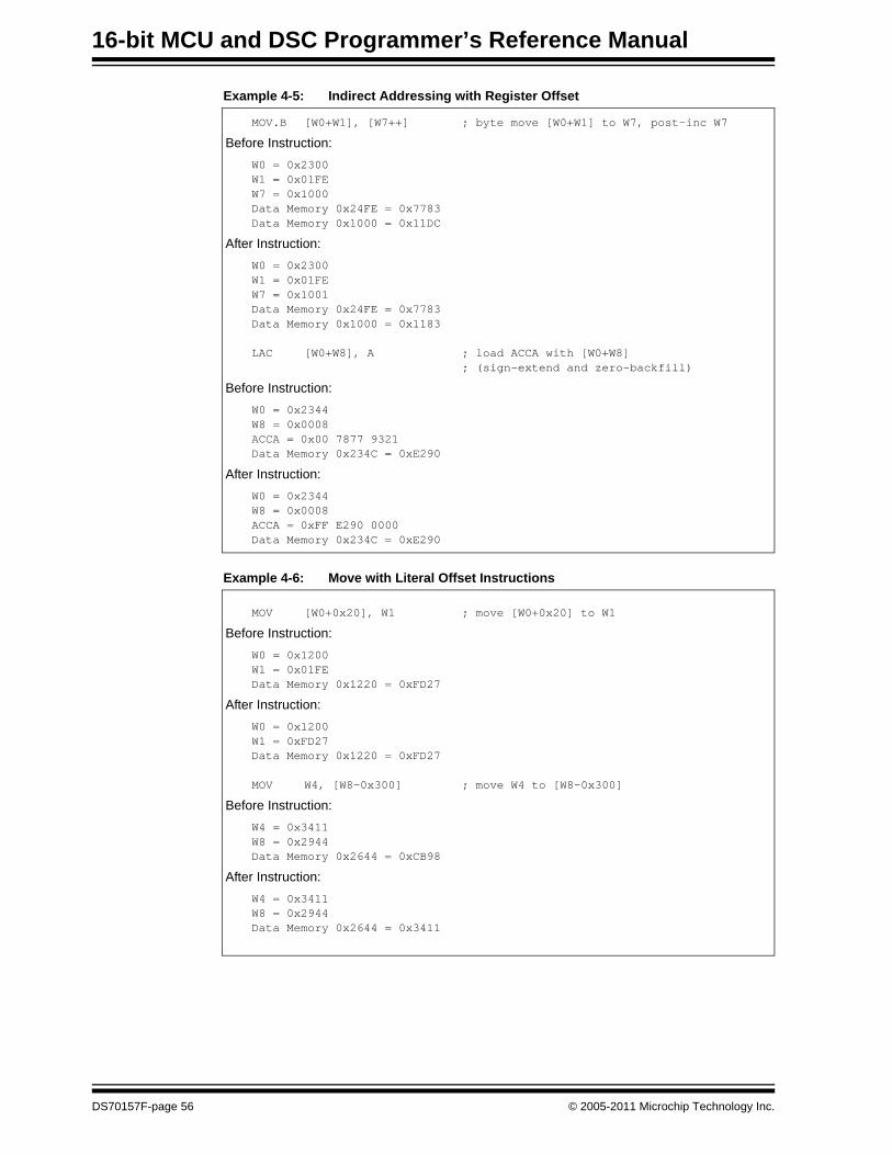
16-bit MCU and DSC Programmer’s Reference Manual
Example 4-5: Indirect Addressing with Register Offset
Example 4-6: Move with Literal Offset Instructions
MOV.B [W0+W1], [W7++] ; byte move [W0+W1] to W7, post-inc W7
Before Instruction:W0 = 0x2300W1 = 0x01FEW7 = 0x1000Data Memory 0x24FE = 0x7783Data Memory 0x1000 = 0x11DC
After Instruction:W0 = 0x2300W1 = 0x01FEW7 = 0x1001Data Memory 0x24FE = 0x7783Data Memory 0x1000 = 0x1183
LAC [W0+W8], A ; load ACCA with [W0+W8]; (sign-extend and zero-backfill)
Before Instruction:W0 = 0x2344W8 = 0x0008ACCA = 0x00 7877 9321Data Memory 0x234C = 0xE290
After Instruction:W0 = 0x2344W8 = 0x0008ACCA = 0xFF E290 0000Data Memory 0x234C = 0xE290
MOV [W0+0x20], W1 ; move [W0+0x20] to W1
Before Instruction:W0 = 0x1200W1 = 0x01FEData Memory 0x1220 = 0xFD27
After Instruction:W0 = 0x1200W1 = 0xFD27Data Memory 0x1220 = 0xFD27
MOV W4, [W8-0x300] ; move W4 to [W8-0x300]
Before Instruction:W4 = 0x3411W8 = 0x2944Data Memory 0x2644 = 0xCB98
After Instruction:W4 = 0x3411W8 = 0x2944Data Memory 0x2644 = 0x3411
DS70157F-page 56 © 2005-2011 Microchip Technology Inc.

Section 4. Instruction Set DetailsInstruction Set
Details
4
4.1.3.1 REGISTER INDIRECT ADDRESSING AND THE INSTRUCTION SET
The Addressing modes presented in Table 4-2 demonstrate the Indirect Addressing mode capability of the 16-bit MCU and DSC devices. Due to operation encoding and functional considerations, not every instruction which supports indirect addressing supports all modes shown in Table 4-2. The majority of instructions which use indirect addressing support the No Modify, Pre-Increment, Pre-Decrement, Post-Increment and Post-Decrement Addressing modes. The MOV instructions, and several accumulator-based DSP instructions (dsPIC30F, dsPIC33F, and dsPIC33E devices only), are also capable of using the Register Offset Addressing mode.
4.1.3.2 DSP MAC INDIRECT ADDRESSING MODES (dsPIC30F, dsPIC33F, AND dsPIC33E DEVICES)
A special class of Indirect Addressing modes is utilized by the DSP MAC instructions. As is described later in Section 4.14 “DSP MAC Instructions (dsPIC30F, dsPIC33F and dsPIC33E Devices)”, the DSP MAC class of instructions are capable of performing two fetches from memory using effective addressing. Since DSP algorithms frequently demand a broader range of address updates, the Addressing modes offered by the DSP MAC instructions provide greater range in the size of the effective address update which may be made. Table 4-3 shows that both X and Y prefetches support Post-Increment and Post-Decrement Addressing modes, with updates of 2, 4 and 6 bytes. Since DSP instructions only execute in Word mode, no provisions are made for odd sized EA updates.
Table 4-3: DSP MAC Indirect Addressing Modes
4.1.3.3 MODULO AND BIT-REVERSED ADDRESSING MODES (dsPIC30F, dsPIC33F, AND dsPIC33E DEVICES)
The 16-bit DSC architecture provides support for two special Register Indirect Addressing modes, which are commonly used to implement DSP algorithms. Modulo (or circular) addressing provides an automated means to support circular data buffers in X and/or Y memory. Modulo buffers remove the need for software to perform address boundary checks, which can improve the performance of certain algorithms. Similarly, bit-reversed addressing allows one to access the elements of a buffer in a nonlinear fashion. This Addressing mode simplifies data re-ordering for radix-2 FFT algorithms and provides a significant reduction in FFT processing time.
Both of these Addressing modes are powerful features of the dsPIC30F, dsPIC33F, and dsPIC33E architectures, which can be exploited by any instruction that uses indirect addressing. Refer to the specific device family reference manual for details on using modulo and bit-reversed addressing.
Note: Instructions which use register indirect addressing use the operand symbols Wd and Ws in the summary tables of Section 3. “Instruction Set Overview”.
Addressing Mode X Memory Y Memory
Indirect with no modification EA = [Wx] EA = [Wy]Indirect with Post-Increment by 2 EA = [Wx] + = 2 EA = [Wy] + = 2Indirect with Post-Increment by 4 EA = [Wx] + = 4 EA = [Wy] + = 4Indirect with Post-Increment by 6 EA = [Wx] + = 6 EA = [Wy] + = 6Indirect with Post-Decrement by 2 EA = [Wx] – = 2 EA = [Wy] – = 2Indirect with Post-Decrement by 4 EA = [Wx] – = 4 EA = [Wy] – = 4Indirect with Post-Decrement by 6 EA = [Wx] – = 6 EA = [Wy] – = 6Indirect with Register Offset EA = [W9 + W12] EA = [W11 + W12]Note: As described in Section 4.14 “DSP MAC Instructions (dsPIC30F, dsPIC33F and
dsPIC33E Devices)”, only W8 and W9 may be used to access X Memory, and only W10 and W11 may be used to access Y Memory.
© 2005-2011 Microchip Technology Inc. DS70157F-page 57
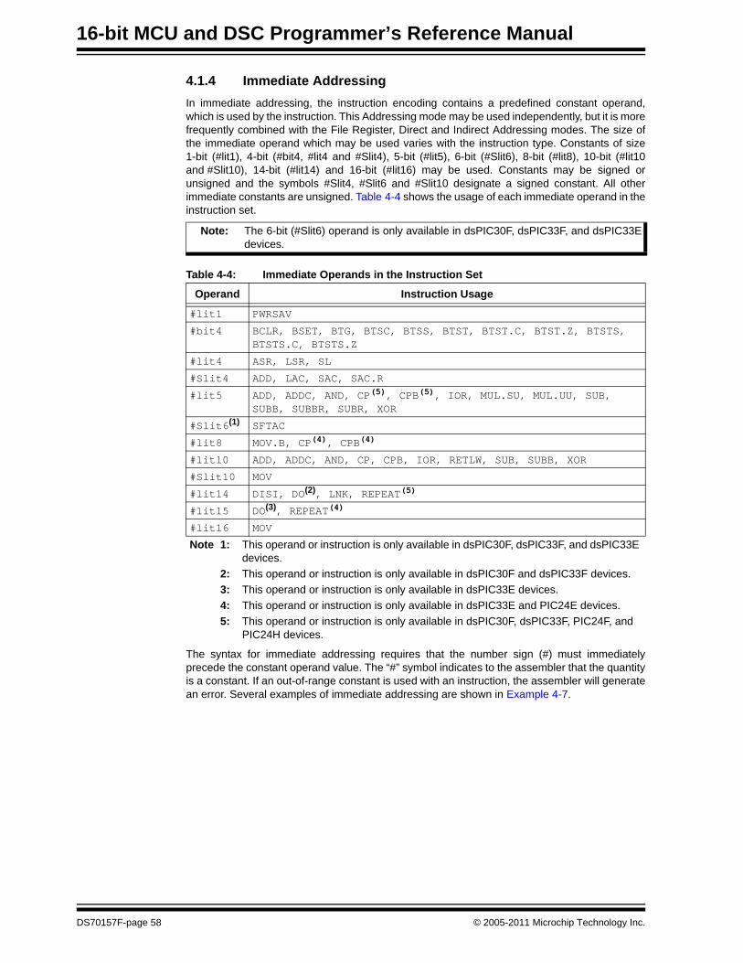
16-bit MCU and DSC Programmer’s Reference Manual
4.1.4 Immediate AddressingIn immediate addressing, the instruction encoding contains a predefined constant operand, which is used by the instruction. This Addressing mode may be used independently, but it is more frequently combined with the File Register, Direct and Indirect Addressing modes. The size of the immediate operand which may be used varies with the instruction type. Constants of size 1-bit (#lit1), 4-bit (#bit4, #lit4 and #Slit4), 5-bit (#lit5), 6-bit (#Slit6), 8-bit (#lit8), 10-bit (#lit10 and #Slit10), 14-bit (#lit14) and 16-bit (#lit16) may be used. Constants may be signed or unsigned and the symbols #Slit4, #Slit6 and #Slit10 designate a signed constant. All other immediate constants are unsigned. Table 4-4 shows the usage of each immediate operand in the instruction set.
Table 4-4: Immediate Operands in the Instruction Set
The syntax for immediate addressing requires that the number sign (#) must immediately precede the constant operand value. The “#” symbol indicates to the assembler that the quantity is a constant. If an out-of-range constant is used with an instruction, the assembler will generate an error. Several examples of immediate addressing are shown in Example 4-7.
Note: The 6-bit (#Slit6) operand is only available in dsPIC30F, dsPIC33F, and dsPIC33E devices.
Operand Instruction Usage
#lit1 PWRSAV
#bit4 BCLR, BSET, BTG, BTSC, BTSS, BTST, BTST.C, BTST.Z, BTSTS, BTSTS.C, BTSTS.Z
#lit4 ASR, LSR, SL
#Slit4 ADD, LAC, SAC, SAC.R
#lit5 ADD, ADDC, AND, CP(5), CPB(5), IOR, MUL.SU, MUL.UU, SUB, SUBB, SUBBR, SUBR, XOR
#Slit6(1) SFTAC
#lit8 MOV.B, CP(4), CPB(4)
#lit10 ADD, ADDC, AND, CP, CPB, IOR, RETLW, SUB, SUBB, XOR
#Slit10 MOV
#lit14 DISI, DO(2), LNK, REPEAT(5)
#lit15 DO(3), REPEAT(4)
#lit16 MOV
Note 1: This operand or instruction is only available in dsPIC30F, dsPIC33F, and dsPIC33E devices.
2: This operand or instruction is only available in dsPIC30F and dsPIC33F devices.3: This operand or instruction is only available in dsPIC33E devices.4: This operand or instruction is only available in dsPIC33E and PIC24E devices.5: This operand or instruction is only available in dsPIC30F, dsPIC33F, PIC24F, and
PIC24H devices.
DS70157F-page 58 © 2005-2011 Microchip Technology Inc.

Section 4. Instruction Set DetailsInstruction Set
Details
4
Example 4-7: Immediate Addressing
4.1.5 Data Addressing Mode TreeThe Data Addressing modes of the PIC24F, PIC24H, and PIC24E families are summarized in Figure 4-1.
Figure 4-1: Data Addressing Mode Tree (PIC24F, PIC24H, and PIC24E)
The Data Addressing modes of the dsPIC30F, dsPIC33F, and dsPIC33E are summarized in Figure 4-2.
PWRSAV #1 ; Enter IDLE mode
ADD.B #0x10, W0 ; Add 0x10 to W0 (byte mode)
Before Instruction:W0 = 0x12A9
After Instruction:W0 = 0x12B9
XOR W0, #1, [W1++] ; Exclusive-OR W0 and 0x1; Store the result to [W1]; Post-increment W1
Before Instruction:W0 = 0xFFFFW1 = 0x0890Data Memory 0x0890 = 0x0032
After Instruction:W0 = 0xFFFFW1 = 0x0892Data Memory 0x0890 = 0xFFFE
Data Addressing Modes
Immediate
File Register
Pre-Increment
Pre-Decrement
Post-Increment
Post-Decrement
Register Offset
Literal Offset
No Modification
Direct
Indirect
© 2005-2011 Microchip Technology Inc. DS70157F-page 59

16-bit MCU and DSC Programmer’s Reference Manual
Figure 4-2: Data Addressing Mode Tree (dsPIC30F, dsPIC33F, and dsPIC33E)
Data Addressing Modes
Immediate
BasicFile Register
Pre-Increment
Pre-Decrement
Post-Increment
Post-Decrement
Register Offset
Literal Offset
No Modification
No Modification
Post-Decrement (2, 4 and 6)
Register Offset
Post-Increment (2, 4 and 6)
DSP MAC
Direct
Indirect
Direct
Indirect
DS70157F-page 60 © 2005-2011 Microchip Technology Inc.

Section 4. Instruction Set DetailsInstruction Set
Details
4
4.2 PROGRAM ADDRESSING MODESThe 16-bit MCU and DSC devices have a 24-bit Program Counter (PC). The PC addresses the 24-bit wide program memory to fetch instructions for execution, and it may be loaded in several ways. For byte compatibility with the table read and table write instructions, each instruction word consumes two locations in program memory. This means that during serial execution, the PC is loaded with PC + 2.
Several methods may be used to modify the PC in a non-sequential manner, and both absolute and relative changes may be made to the PC. The change to the PC may be from an immediate value encoded in the instruction, or a dynamic value contained in a working register. In dsPIC30F, dsPIC33F, and dsPIC33E devices, when DO looping is active, the PC is loaded with the address stored in the DOSTART register, after the instruction at the DOEND address is executed. For exception handling, the PC is loaded with the address of the exception handler, which is stored in the interrupt vector table. When required, the software stack is used to return scope to the foreground process from where the change in program flow occurred.
Table 4-5 summarizes the instructions which modify the PC. When performing function calls, it is recommended that RCALL be used instead of CALL, since RCALL only consumes 1 word of program memory.
Table 4-5: Methods of Modifying Program Flow
Condition/Instruction PC Modification Software Stack Usage
Sequential Execution PC = PC + 2 NoneBRA Expr(1)
(Branch Unconditionally)PC = PC + 2*Slit16 None
BRA Condition, Expr(1)
(Branch Conditionally)PC = PC + 2 (condition false)PC = PC + 2 * Slit16 (condition true)
None
CALL Expr(1)
(Call Subroutine)PC = lit23 PC + 4 is PUSHed on the stack(2)
CALL Wn(Call Subroutine Indirect)
PC = Wn PC + 2 is PUSHed on the stack(2)
CALL.L Wn(5)
(Call Indirect Subroutine Long)PC = {Wn+1:Wn} None
GOTO Expr(1)
(Unconditional Jump)PC = lit23 None
GOTO Wn(Unconditional Indirect Jump)
PC = Wn None
GOTO.L Wn(5)
(Unconditional Indirect Long Jump)PC = {Wn+1:Wn} None
RCALL Expr(1)
(Relative Call)PC = PC + 2 * Slit16 PC + 2 is PUSHed on the stack(2)
RCALL Wn(Computed Relative Call)
PC = PC + 2 * Wn PC + 2 is PUSHed on the stack(2)
Exception Handling PC = address of the exception handler(read from vector table)
PC + 2 is PUSHed on the stack(3)
PC = Target REPEAT instruction(REPEAT Looping)
PC not modified (if REPEAT active) None
PC = DOEND address(4)
(DO Looping)PC = DOSTART (if DO active) None
Note 1: For BRA, CALL and GOTO, the Expr may be a label, absolute address, or expression, which is resolved by the linker to a 16-bit or 23-bit value (Slit16 or lit23). See Section 5. “Instruction Descriptions” for details.
2: After CALL or RCALL is executed, RETURN or RETLW will POP the Top-of-Stack (TOS) back into the PC.3: After an exception is processed, RETFIE will POP the Top-of-Stack (TOS) back into the PC.4: This condition/instruction is only available in dsPIC30F, dsPIC33F, and dsPIC33E devices.5: This condition instruction is only available in dsPIC33E and PIC24E devices.
© 2005-2011 Microchip Technology Inc. DS70157F-page 61

16-bit MCU and DSC Programmer’s Reference Manual
4.3 INSTRUCTION STALLSIn order to maximize the data space EA calculation and operand fetch time, the X data space read and write accesses are partially pipelined. A consequence of this pipelining is that address register data dependencies may arise between successive read and write operations using common registers.
‘Read After Write’ (RAW) dependencies occur across instruction boundaries and are detected by the hardware. An example of a RAW dependency would be a write operation that modifies W5, followed by a read operation that uses W5 as an Address Pointer. The contents of W5 will not be valid for the read operation until the earlier write completes. This problem is resolved by stalling the instruction execution for one instruction cycle, which allows the write to complete before the next read is started.
4.3.1 RAW Dependency DetectionDuring the instruction pre-decode, the core determines if any address register dependency is imminent across an instruction boundary. The stall detection logic compares the W register (if any) used for the destination EA of the instruction currently being executed with the W register to be used by the source EA (if any) of the prefetched instruction. When a match between the destination and source registers is identified, a set of rules are applied to decide whether or not to stall the instruction by one cycle. Table 4-6 lists various RAW conditions which cause an instruction execution stall.
Table 4-6: Raw Dependency Rules (Detection By Hardware)
DestinationAddress Mode
Using Wn
Source Address Mode
Using Wn
Stall Required?
Examples(2)
(Wn = W2)
Direct Direct No Stall ADD.W W0, W1, W2MOV.W W2, W3
Indirect Direct No Stall ADD.W W0, W1, [W2]MOV.W W2, W3
Indirect Indirect No Stall ADD.W W0, W1, [W2]MOV.W [W2], W3
Indirect Indirect with pre/post-modification
No Stall ADD.W W0, W1, [W2]MOV.W [W2++], W3
Indirect with pre/post-modification
Direct No Stall ADD.W W0, W1, [W2++]MOV.W W2, W3
Direct Indirect Stall(1) ADD.W W0, W1, W2MOV.W [W2], W3
Direct Indirect with pre/post-modification
Stall(1) ADD.W W0, W1, W2MOV.W [W2++], W3
Indirect Indirect Stall(1) ADD.W W0, W1, [W2](2)MOV.W [W2], W3(2)
Indirect Indirect with pre/post-modification
Stall(1) ADD.W W0, W1, [W2](2) MOV.W [W2++], W3(2)
Indirect with pre/post-modification
Indirect Stall(1) ADD.W W0, W1, [W2++]MOV.W [W2], W3
Indirect with pre/post-modification
Indirect with pre/post-modification
Stall(1) ADD.W W0, W1, [W2++]MOV.W [W2++], W3
Note 1: When stalls are detected, one cycle is added to the instruction execution time.2: For these examples, the contents of W2 = the mapped address of W2 (0x0004).
DS70157F-page 62 © 2005-2011 Microchip Technology Inc.
Section 4. Instruction Set DetailsInstruction Set
Details
4
4.3.2 Instruction Stalls and ExceptionsIn order to maintain deterministic operation, instruction stalls are allowed to happen, even if they occur immediately prior to exception processing.
4.3.3 Instruction Stalls and Instructions that Change Program FlowCALL and RCALL write to the stack using W15 and may, therefore, be subject to an instruction stall if the source read of the subsequent instruction uses W15.
GOTO, RETFIE and RETURN instructions are never subject to an instruction stall because they do not perform write operations to the working registers.
4.3.4 Instruction Stalls and DO/REPEAT LoopsInstructions operating in a DO or REPEAT loop are subject to instruction stalls, just like any other instruction. Stalls may occur on loop entry, loop exit and also during loop processing.
4.3.5 Instruction Stalls and PSVInstructions operating in PSV address space are subject to instruction stalls, just like any other instruction. Should a data dependency be detected in the instruction immediately following the PSV data access, the second cycle of the instruction will initiate a stall. Should a data dependency be detected in the instruction immediately before the PSV data access, the last cycle of the previous instruction will initiate a stall.
Note: DO loops are only available in dsPIC30F, dsPIC33F, and dsPIC33E devices.
Note: Refer to the specific device family reference manual for more detailed information about RAW instruction stalls.
© 2005-2011 Microchip Technology Inc. DS70157F-page 63

16-bit MCU and DSC Programmer’s Reference Manual
4.4 BYTE OPERATIONSSince the data memory is byte addressable, most of the base instructions may operate in either Byte mode or Word mode. When these instructions operate in Byte mode, the following rules apply:
• All direct working register references use the Least Significant Byte of the 16-bit working register and leave the Most Significant Byte (MSB) unchanged
• All indirect working register references use the data byte specified by the 16-bit address stored in the working register
• All file register references use the data byte specified by the byte address• The STATUS Register is updated to reflect the result of the byte operation
It should be noted that data addresses are always represented as byte addresses. Additionally, the native data format is little-endian, which means that words are stored with the Least Significant Byte at the lower address, and the Most Significant Byte at the adjacent, higher address (as shown in Figure 4-3). Example 4-8 shows sample byte move operations and Example 4-9 shows sample byte math operations.
Example 4-8: Sample Byte Move Operations
Note: Instructions that operate in Byte mode must use the “.b” or “.B” instruction extension to specify a byte instruction. For example, the following two instructions are valid forms of a byte clear operation:
• CLR.b W0
• CLR.B W0
MOV.B #0x30, W0 ; move the literal byte 0x30 to W0
Before Instruction:W0 = 0x5555
After Instruction:W0 = 0x5530
MOV.B 0x1000, W0 ; move the byte at 0x1000 to W0
Before Instruction:W0 = 0x5555Data Memory 0x1000 = 0x1234
After Instruction:W0 = 0x5534Data Memory 0x1000 = 0x1234
MOV.B W0, 0x1001 ; byte move W0 to address 0x1001
Before Instruction:W0 = 0x1234Data Memory 0x1000 = 0x5555
After Instruction:W0 = 0x1234Data Memory 0x1000 = 0x3455
MOV.B W0, [W1++] ; byte move W0 to [W1], then post-inc W1
Before Instruction:W0 = 0x1234W1 = 0x1001Data Memory 0x1000 = 0x5555
After Instruction:W0 = 0x1234W1 = 0x1002Data Memory 0x1000 = 0x3455
DS70157F-page 64 © 2005-2011 Microchip Technology Inc.

Section 4. Instruction Set DetailsInstruction Set
Details
4
Example 4-9: Sample Byte Math OperationsCLR.B [W6--] ; byte clear [W6], then post-dec W6
Before Instruction:W6 = 0x1001Data Memory 0x1000 = 0x5555
After Instruction:W6 = 0x1000Data Memory 0x1000 = 0x0055
SUB.B W0, #0x10, W1 ; byte subtract literal 0x10 from W0; and store to W1
Before Instruction:W0 = 0x1234W1 = 0xFFFF
After Instruction:W0 = 0x1234W1 = 0xFF24
ADD.B W0, W1, [W2++] ; byte add W0 and W1, store to [W2]; and post-inc W2
Before Instruction:W0 = 0x1234W1 = 0x5678W2 = 0x1000Data Memory 0x1000 = 0x5555
After Instruction:W0 = 0x1234W1 = 0x5678W2 = 0x1001Data Memory 0x1000 = 0x55AC
© 2005-2011 Microchip Technology Inc. DS70157F-page 65

16-bit MCU and DSC Programmer’s Reference Manual
4.5 WORD MOVE OPERATIONSEven though the data space is byte addressable, all move operations made in Word mode must be word-aligned. This means that for all source and destination operands, the Least Significant address bit must be ‘0’. If a word move is made to or from an odd address, an address error exception is generated. Likewise, all double words must be word-aligned. Figure 4-3 shows how bytes and words may be aligned in data memory. Example 4-10 contains several legal word move operations.
When an exception is generated due to a misaligned access, the exception is taken after the instruction executes. If the illegal access occurs from a data read, the operation will be allowed to complete, but the Least Significant bit of the source address will be cleared to force word alignment. If the illegal access occurs during a data write, the write will be inhibited. Example 4-11 contains several illegal word move operations.
Figure 4-3: Data Alignment in Memory
0x1001 b0 0x10000x1003 b1 0x10020x1005 b3 b2 0x10040x1007 b5 b4 0x10060x1009 b7 b6 0x10080x100B b8 0x100A
Legend: b0 – byte stored at 0x1000 b1 – byte stored at 0x1003 b3:b2 – word stored at 0x1005:1004 (b2 is LSB) b7:b4 – double word stored at 0x1009:0x1006 (b4 is LSB) b8 – byte stored at 0x100A
Note: Instructions that operate in Word mode are not required to use an instruction extension. However, they may be specified with an optional “.w” or “.W” extension, if desired. For example, the following instructions are valid forms of a word clear operation:
• CLR W0
• CLR.w W0
• CLR.W W0
DS70157F-page 66 © 2005-2011 Microchip Technology Inc.
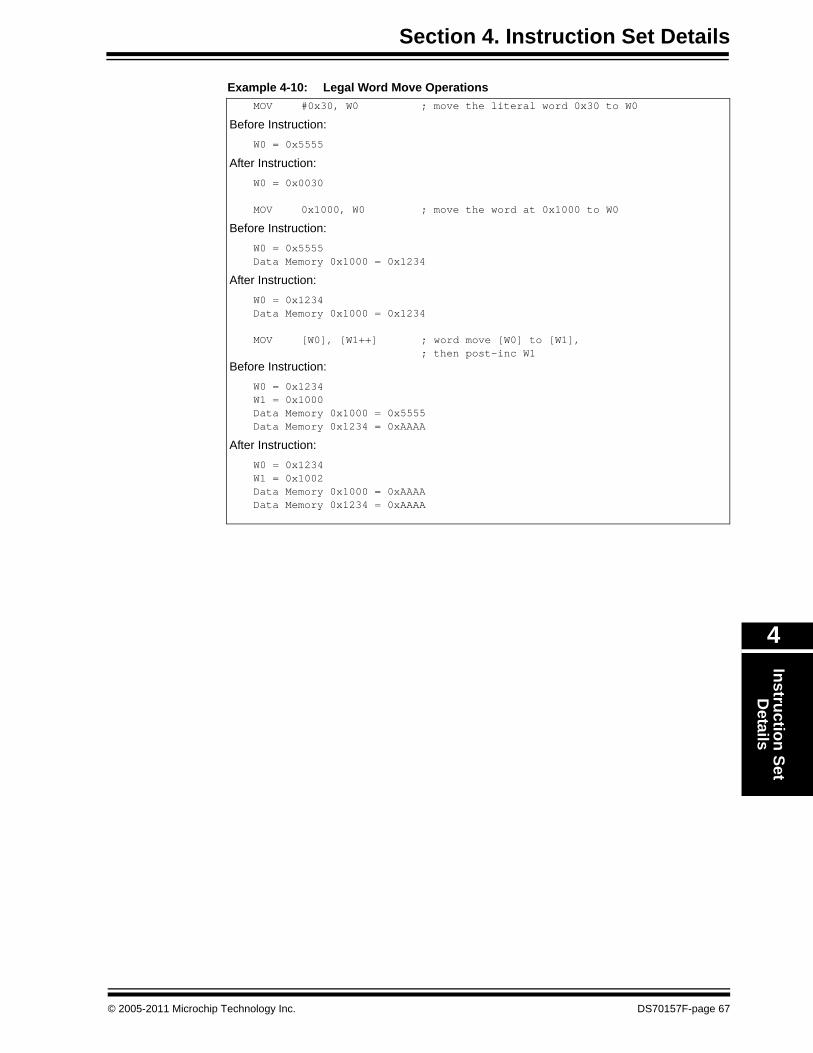
Section 4. Instruction Set DetailsInstruction Set
Details
4
Example 4-10: Legal Word Move OperationsMOV #0x30, W0 ; move the literal word 0x30 to W0
Before Instruction:W0 = 0x5555
After Instruction:W0 = 0x0030
MOV 0x1000, W0 ; move the word at 0x1000 to W0
Before Instruction:W0 = 0x5555Data Memory 0x1000 = 0x1234
After Instruction:W0 = 0x1234Data Memory 0x1000 = 0x1234
MOV [W0], [W1++] ; word move [W0] to [W1],; then post-inc W1
Before Instruction:W0 = 0x1234W1 = 0x1000Data Memory 0x1000 = 0x5555Data Memory 0x1234 = 0xAAAA
After Instruction:W0 = 0x1234W1 = 0x1002Data Memory 0x1000 = 0xAAAAData Memory 0x1234 = 0xAAAA
© 2005-2011 Microchip Technology Inc. DS70157F-page 67

16-bit MCU and DSC Programmer’s Reference Manual
Example 4-11: Illegal Word Move OperationsMOV 0x1001, W0 ; move the word at 0x1001 to W0
Before Instruction:W0 = 0x5555Data Memory 0x1000 = 0x1234Data Memory 0x1002 = 0x5678
After Instruction:W0 = 0x1234Data Memory 0x1000 = 0x1234Data Memory 0x1002 = 0x5678
ADDRESS ERROR TRAP GENERATED
(source address is misaligned, so MOV is performed)
MOV W0, 0x1001 ; move W0 to the word at 0x1001
Before Instruction:W0 = 0x1234Data Memory 0x1000 = 0x5555Data Memory 0x1002 = 0x6666
After Instruction:W0 = 0x1234Data Memory 0x1000 = 0x5555Data Memory 0x1002 = 0x6666
ADDRESS ERROR TRAP GENERATED
(destination address is misaligned, so MOV is not performed)
MOV [W0], [W1++] ; word move [W0] to [W1], ; then post-inc W1
Before Instruction:W0 = 0x1235W1 = 0x1000Data Memory 0x1000 = 0x1234Data Memory 0x1234 = 0xAAAAData Memory 0x1236 = 0xBBBB
After Instruction:W0 = 0x1235W1 = 0x1002Data Memory 0x1000 = 0xAAAAData Memory 0x1234 = 0xAAAAData Memory 0x1236 = 0xBBBB
ADDRESS ERROR TRAP GENERATED
(source address is misaligned, so MOV is performed)
DS70157F-page 68 © 2005-2011 Microchip Technology Inc.

Section 4. Instruction Set DetailsInstruction Set
Details
4
4.6 USING 10-BIT LITERAL OPERANDSSeveral instructions that support Byte and Word mode have 10-bit operands. For byte instructions, a 10-bit literal is too large to use. So when 10-bit literals are used in Byte mode, the range of the operand must be reduced to 8 bits or the assembler will generate an error. Table 4-7 shows that the range of a 10-bit literal is 0:1023 in Word mode and 0:255 in Byte mode.
Instructions which employ 10-bit literals in Byte and Word mode are: ADD, ADDC, AND, IOR, RETLW, SUB, SUBB, and XOR. Example 4-12 shows how positive and negative literals are used in Byte mode for the ADD instruction.
Table 4-7: 10-bit Literal Coding
Example 4-12: Using 10-bit Literals for Byte Operands
Literal Value Word Modekk kkkk kkkk
Byte Modekkkk kkkk
0 00 0000 0000 0000 0000
1 00 0000 0001 0000 0001
2 00 0000 0010 0000 0010
127 00 0111 1111 0111 1111
128 00 1000 0000 1000 0000
255 00 1111 1111 1111 1111
256 01 0000 0000 N/A512 10 0000 0000 N/A
1023 11 1111 1111 N/A
ADD.B #0x80, W0 ; add 128 (or -128) to W0ADD.B #0x380, W0 ; ERROR... Illegal syntax for byte mode ADD.B #0xFF, W0 ; add 255 (or -1) to W0ADD.B #0x3FF, W0 ; ERROR... Illegal syntax for byte modeADD.B #0xF, W0 ; add 15 to W0ADD.B #0x7F, W0 ; add 127 to W0ADD.B #0x100, W0 ; ERROR... Illegal syntax for byte mode
Note: Using a literal value greater than 127 in Byte mode is functionally identical to using the equivalent negative two’s complement value, since the Most Significant bit of the byte is set. When operating in Byte mode, the Assembler will accept either a positive or negative literal value (i.e., #-10).
© 2005-2011 Microchip Technology Inc. DS70157F-page 69

16-bit MCU and DSC Programmer’s Reference Manual
4.7 SOFTWARE STACK POINTER AND FRAME POINTER
4.7.1 Software Stack PointerThe 16-bit MCU and DSC devices feature a software stack which facilitates function calls and exception handling. W15 is the default Stack Pointer (SP) and after any Reset, it is initialized to 0x0800 (0x1000 for PIC24E and dsPIC33E devices). This ensures that the SP will point to valid RAM and permits stack availability for exceptions, which may occur before the SP is set by the user software. The user may reprogram the SP during initialization to any location within data space.
The SP always points to the first available free word (Top-of-Stack) and fills the software stack, working from lower addresses towards higher addresses. It pre-decrements for a stack POP(read) and post-increments for a stack PUSH (write).
The software stack is manipulated using the PUSH and POP instructions. The PUSH and POPinstructions are the equivalent of a MOV instruction, with W15 used as the destination pointer. For example, the contents of W0 can be PUSHed onto the Top-of-Stack (TOS) by:
PUSH W0
This syntax is equivalent to:MOV W0,[W15++]
The contents of the TOS can be returned to W0 by: POP W0
This syntax is equivalent to:MOV [--W15],W0
During any CALL instruction, the PC is PUSHed onto the stack, such that when the subroutine completes execution, program flow may resume from the correct location. When the PC is PUSHed onto the stack, PC<15:0> is PUSHed onto the first available stack word, then PC<22:16> is PUSHed. When PC<22:16> is PUSHed, the Most Significant 7 bits of the PC are zero-extended before the PUSH is made, as shown in Figure 4-4. During exception processing, the Most Significant 7 bits of the PC are concatenated with the lower byte of the STATUS register (SRL) and IPL<3>, CORCON<3>. This allows the primary STATUS register contents and CPU Interrupt Priority Level to be automatically preserved during interrupts.
Figure 4-4: Stack Operation for CALL Instruction
Note: In order to protect against misaligned stack accesses, W15<0> is always clear.
015
W15 (before CALL)
W15 (after CALL)
Stac
k G
row
s To
war
dsH
ighe
r Add
ress
0x0000
PC<15:0> 0x0 PC<22:16>
Top-of-Stack
0xFFFE
Note: For exceptions, the upper nine bits of the second PUSHed word contains the SRL and IPL<3>.
DS70157F-page 70 © 2005-2011 Microchip Technology Inc.
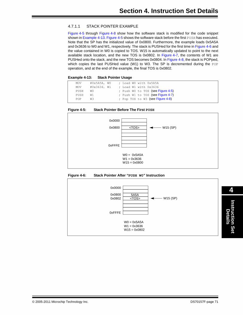
Section 4. Instruction Set DetailsInstruction Set
Details
4
4.7.1.1 STACK POINTER EXAMPLE
Figure 4-5 through Figure 4-8 show how the software stack is modified for the code snippet shown in Example 4-13. Figure 4-5 shows the software stack before the first PUSH has executed. Note that the SP has the initialized value of 0x0800. Furthermore, the example loads 0x5A5A and 0x3636 to W0 and W1, respectively. The stack is PUSHed for the first time in Figure 4-6 and the value contained in W0 is copied to TOS. W15 is automatically updated to point to the next available stack location, and the new TOS is 0x0802. In Figure 4-7, the contents of W1 are PUSHed onto the stack, and the new TOS becomes 0x0804. In Figure 4-8, the stack is POPped, which copies the last PUSHed value (W1) to W3. The SP is decremented during the POPoperation, and at the end of the example, the final TOS is 0x0802.
Example 4-13: Stack Pointer Usage
Figure 4-5: Stack Pointer Before The First PUSH
Figure 4-6: Stack Pointer After “PUSH W0” Instruction
MOV #0x5A5A, W0 ; Load W0 with 0x5A5AMOV #0x3636, W1 ; Load W1 with 0x3636PUSH W0 ; Push W0 to TOS (see Figure 4-5)PUSH W1 ; Push W1 to TOS (see Figure 4-7)POP W3 ; Pop TOS to W3 (see Figure 4-8)
0x0000
0xFFFE
0x0800 W15 (SP)
W15 = 0x0800
W0 = 0x5A5AW1 = 0x3636
<TOS>
0x0000
0xFFFE
0x0800W15 (SP)
W15 = 0x0802
W0 = 0x5A5AW1 = 0x3636
5A5A<TOS>0x0802
© 2005-2011 Microchip Technology Inc. DS70157F-page 71

16-bit MCU and DSC Programmer’s Reference Manual
Figure 4-7: Stack Pointer After “PUSH W1” Instruction
Figure 4-8: Stack Pointer After “POP W3” Instruction
4.7.2 Software Stack Frame PointerA Stack Frame is a user-defined section of memory residing in the software stack. It is used to allocate memory for temporary variables which a function uses, and one Stack Frame may be created for each function. W14 is the default Stack Frame Pointer (FP) and it is initialized to 0x0000 on any Reset. If the Stack Frame Pointer is not used, W14 may be used like any other working register.
The link (LNK) and unlink (ULNK) instructions provide Stack Frame functionality. The LNKinstruction is used to create a Stack Frame. It is used during a call sequence to adjust the SP, such that the stack may be used to store temporary variables utilized by the called function. After the function completes execution, the ULNK instruction is used to remove the Stack Frame created by the LNK instruction. The LNK and ULNK instructions must always be used together to avoid stack overflow.
0x0000
0xFFFE
0x0800
W15 (SP)
W15 = 0x0804
W0 = 0x5A5AW1 = 0x3636
5A5A
<TOS>0x0802 36360x0804
0x0000
0xFFFE
0x0800W15 (SP)
W15 = 0x0802
W0 = 0x5A5AW1 = 0x3636
5A5A0x0802 <TOS>0x0804
W3 = 0x3636
Note: The contents of 0x802, the new TOS, remain unchanged (0x3636).
DS70157F-page 72 © 2005-2011 Microchip Technology Inc.
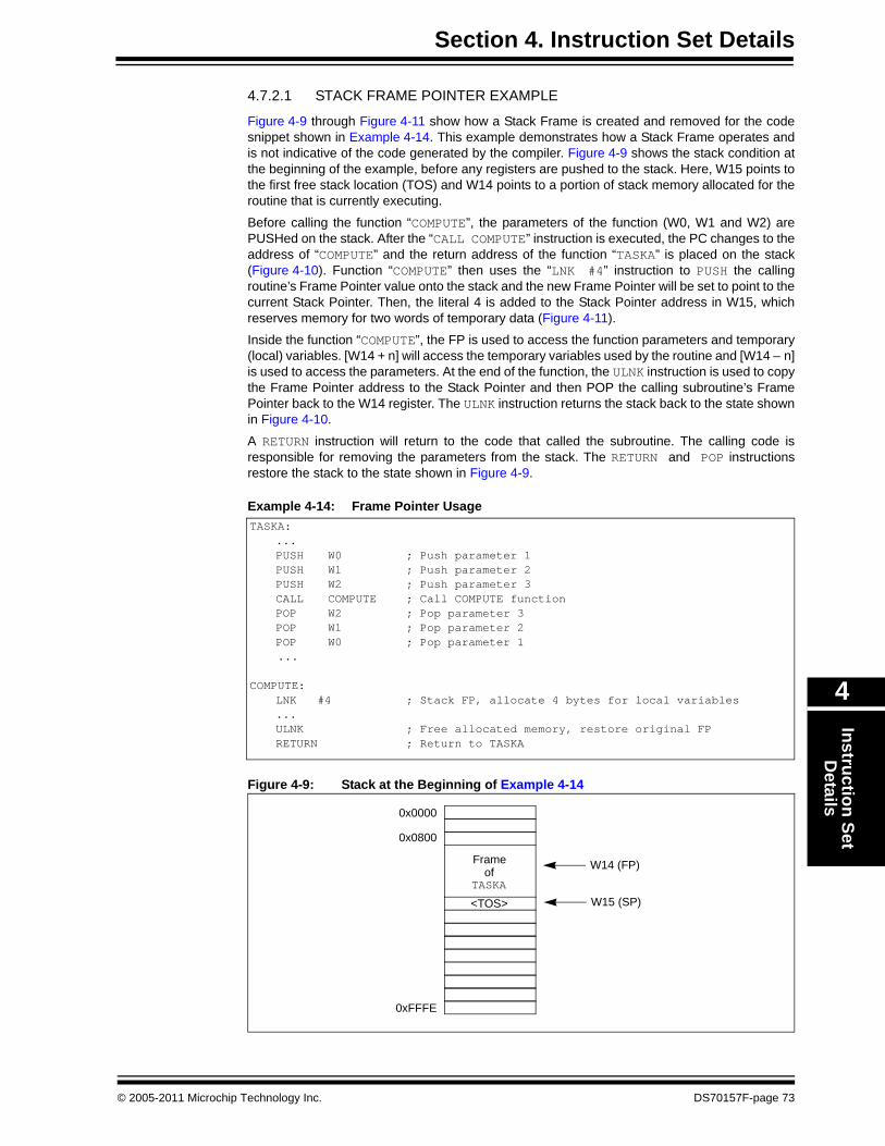
Section 4. Instruction Set DetailsInstruction Set
Details
4
4.7.2.1 STACK FRAME POINTER EXAMPLE
Figure 4-9 through Figure 4-11 show how a Stack Frame is created and removed for the code snippet shown in Example 4-14. This example demonstrates how a Stack Frame operates and is not indicative of the code generated by the compiler. Figure 4-9 shows the stack condition at the beginning of the example, before any registers are pushed to the stack. Here, W15 points to the first free stack location (TOS) and W14 points to a portion of stack memory allocated for the routine that is currently executing.
Before calling the function “COMPUTE”, the parameters of the function (W0, W1 and W2) are PUSHed on the stack. After the “CALL COMPUTE” instruction is executed, the PC changes to the address of “COMPUTE” and the return address of the function “TASKA” is placed on the stack (Figure 4-10). Function “COMPUTE” then uses the “LNK #4” instruction to PUSH the calling routine’s Frame Pointer value onto the stack and the new Frame Pointer will be set to point to the current Stack Pointer. Then, the literal 4 is added to the Stack Pointer address in W15, which reserves memory for two words of temporary data (Figure 4-11).
Inside the function “COMPUTE”, the FP is used to access the function parameters and temporary (local) variables. [W14 + n] will access the temporary variables used by the routine and [W14 – n] is used to access the parameters. At the end of the function, the ULNK instruction is used to copy the Frame Pointer address to the Stack Pointer and then POP the calling subroutine’s Frame Pointer back to the W14 register. The ULNK instruction returns the stack back to the state shown in Figure 4-10.
A RETURN instruction will return to the code that called the subroutine. The calling code is responsible for removing the parameters from the stack. The RETURN and POP instructions restore the stack to the state shown in Figure 4-9.
Example 4-14: Frame Pointer Usage
Figure 4-9: Stack at the Beginning of Example 4-14
TASKA: ... PUSH W0 ; Push parameter 1PUSH W1 ; Push parameter 2PUSH W2 ; Push parameter 3CALL COMPUTE ; Call COMPUTE functionPOP W2 ; Pop parameter 3POP W1 ; Pop parameter 2POP W0 ; Pop parameter 1
...
COMPUTE:LNK #4 ; Stack FP, allocate 4 bytes for local variables...ULNK ; Free allocated memory, restore original FP RETURN ; Return to TASKA
0x0000
0xFFFE
0x0800
W14 (FP)
<TOS> W15 (SP)TASKA
Frameof
© 2005-2011 Microchip Technology Inc. DS70157F-page 73

16-bit MCU and DSC Programmer’s Reference Manual
Figure 4-10: Stack After “CALL COMPUTE” Executes
Figure 4-11: Stack After “LNK #4” Executes
4.7.3 Stack Pointer Overflow There is a Stack Limit register (SPLIM) associated with the Stack Pointer that is reset to 0x0000. SPLIM is a 16-bit register, but SPLIM<0> is fixed to ‘0’, because all stack operations must be word-aligned.
The stack overflow check will not be enabled until a word write to SPLIM occurs, after which time it can only be disabled by a device Reset. All effective addresses generated using W15 as a source or destination are compared against the value in SPLIM. Should the effective address be greater than the contents of SPLIM, then a stack error trap is generated.
If stack overflow checking has been enabled, a stack error trap will also occur if the W15 effective address calculation wraps over the end of data space (0xFFFF).
Refer to the specific device family reference manual for more information on the stack error trap.
0x0000
0xFFFE
0x0800
W14 (FP)
Parameter 1
W15 (SP)
TASKA
Frameof
Parameter 2Parameter 3PC<15:0>(1)
0:PC<22:16><TOS>
Note 1: In dsPIC33E/PIC24E devices, the SFA bit is stacked instead of PC<0>
0x0000
0xFFFE
0x0800
W14 (FP)
Parameter 1
W15 (SP)
TASKA
Frame of
Parameter 2Parameter 3PC<15:0>(1)
0:PC<22:16>
<TOS>
FP of TASKATemp Word 1Temp Word 2
Note 1: In dsPIC33E/PIC24E devices, the SFA bit is stacked instead of PC<0>
DS70157F-page 74 © 2005-2011 Microchip Technology Inc.

Section 4. Instruction Set DetailsInstruction Set
Details
4
4.7.4 Stack Pointer UnderflowThe stack is initialized to 0x0800 during Reset (0x1000 for PIC24E and dsPIC33E devices). A stack error trap will be initiated should the Stack Pointer address ever be less than 0x0800 (0x1000 for PIC24E and dsPIC33E devices).
4.7.5 Stack Frame Active (SFA) Control (dsPIC33E and PIC24E Devices)
W15 is never subject to paging and is therefore restricted to address range 0x000000 to 0x00FFFF. However, the Stack Frame Pointer (W14) for any user software function is only dedicated to that function when a stack frame addressed by W14 is active (i.e., after a LNKinstruction). Therefore, it is desirable to have the ability to dynamically switch W14 between use as a general purpose W register, and use as a Stack Frame Pointer. The SFA Status bit (CORCON<2>) achieves this function without additional software overhead.When the SFA bit is clear, W14 may be used with any page register. When SFA is set, W14 is not subject to paging and is locked into the same address range as W15 (0x000000 to 0x00FFFF). Operation of the SFA register lock is as follows:• The LNK instruction sets SFA (and creates a stack frame)• The ULNK instruction clears SFA (and deletes the stack frame)• The CALL, CALL.L, and RCALL instructions also stack the SFA bit (placing it in the LSb of
the stacked PC), and clear the SFA bit after the stacking operation is complete. The called procedure is now free to either use W14 as a general purpose register, or create another stack frame using the LNK instruction.
• The RETURN, RETLW and RETFIE instructions all restore the SFA bit from its previously stacked value
The SFA bit is a read-only bit. It can only be set by execution of the LNK instruction, and cleared by the ULNK, CALL, CALL.L, and RCALL instructions.
Note: Locations in data space between 0x0000 and 0x07FF (0x0FFF for PIC24E and dsPIC33E devices) are, in general, reserved for core and peripheral Special Function Registers (SFRs).
Note: In dsPIC33E and PIC24E devices, the SFA bit is stacked instead of PC<0>.
© 2005-2011 Microchip Technology Inc. DS70157F-page 75

16-bit MCU and DSC Programmer’s Reference Manual
4.8 CONDITIONAL BRANCH INSTRUCTIONSConditional branch instructions are used to direct program flow, based on the contents of the STATUS register. These instructions are generally used in conjunction with a Compare class instruction, but they may be employed effectively after any operation that modifies the STATUS register.
The compare instructions CP, CP0 and CPB, perform a subtract operation (minuend – subtrahend), but do not actually store the result of the subtraction. Instead, compare instructions just update the flags in the STATUS register, such that an ensuing conditional branch instruction may change program flow by testing the contents of the updated STATUS register. If the result of the STATUS register test is true, the branch is taken. If the result of the STATUS register test is false, the branch is not taken.
The conditional branch instructions supported by the dsPIC30F, dsPIC33F, and dsPIC33E devices are shown in Table 4-8. This table identifies the condition in the STATUS register which must be true for the branch to be taken. In some cases, just a single bit is tested (as in BRA C), while in other cases, a complex logic operation is performed (as in BRA GT). For dsPIC30F, dsPIC33F, and dsPIC33E devices, it is worth noting that both signed and unsigned conditional tests are supported, and that support is provided for DSP algorithms with the OA, OB, SA and SB condition mnemonics.
Table 4-8: Conditional Branch Instructions
Note 1: Instructions are of the form: BRA mnemonic, Expr.2: GEU is identical to C and will reverse assemble to BRA C, Expr.3: LTU is identical to NC and will reverse assemble to BRA NC, Expr.4: This condition is only available in dsPIC30F, dsPIC33F, and dsPIC33E devices.
ConditionMnemonic(1) Description Status Test
C Carry (not Borrow) C
GE Signed greater than or equal (N&&OV) || (N&&OV)
GEU(2) Unsigned greater than or equal C
GT Signed greater than (Z&&N&&OV) || (Z&&N&&OV)
GTU Unsigned greater than C&&Z
LE Signed less than or equal Z || (N&&OV) || (N&&OV)
LEU Unsigned less than or equal C || Z
LT Signed less than (N&&OV) || (N&&OV)
LTU(3) Unsigned less than C
N Negative N
NC Not Carry (Borrow) C
NN Not Negative N
NOV Not Overflow OV
NZ Not Zero Z
OA(4) Accumulator A overflow OA
OB(4) Accumulator B overflow OB
OV Overflow OV
SA(4) Accumulator A saturate SA
SB(4) Accumulator B saturate SB
Z Zero Z
Note: The “Compare and Skip” instructions (CPBEQ, CPBGT, CPBLT, CPBNE, CPSEQ, CPSGT, CPSLT, and CPSNE) do not modify the STATUS register.
DS70157F-page 76 © 2005-2011 Microchip Technology Inc.

Section 4. Instruction Set DetailsInstruction Set
Details
4
4.9 Z STATUS BITThe Z Status bit is a special zero Status bit that is useful for extended precision arithmetic. The Z bit functions like a normal Z flag for all instructions, except those that use the Carry/Borrowinput (ADDC, CPB, SUBB and SUBBR). For the ADDC, CPB, SUBB and SUBBR instructions, the Z bit can only be cleared and never set. If the result of one of these instructions is non-zero, the Z bit will be cleared and will remain cleared, regardless of the result of subsequent ADDC, CPB,SUBB or SUBBR operations. This allows the Z bit to be used for performing a simple zero check on the result of a series of extended precision operations.
A sequence of instructions working on multi-precision data (starting with an instruction with no Carry/Borrow input), will automatically logically AND the successive results of the zero test. All results must be zero for the Z flag to remain set at the end of the sequence of operations. If the result of the ADDC, CPB, SUBB or SUBBR instruction is non-zero, the Z bit will be cleared and remain cleared for all subsequent ADDC, CPB, SUBB or SUBBR instructions. Example 4-15 shows how the Z bit operates for a 32-bit addition. It shows how the Z bit is affected for a 32-bit addition implemented with an ADD/ADDC instruction sequence. The first example generates a zero result for only the most significant word, and the second example generates a zero result for both the least significant word and most significant word.
Example 4-15: ‘Z’ Status bit Operation for 32-bit Addition; Add two doubles (W0:W1 and W2:W3); Store the result in W5:W4ADD W0, W2, W4 ; Add LSWord and store to W4ADDC W1, W3, W5 ; Add MSWord and store to W5
Before 32-bit Addition (zero result for the most significant word):W0 = 0x2342W1 = 0xFFF0W2 = 0x39AAW3 = 0x0010W4 = 0x0000W5 = 0x0000SR = 0x0000
After 32-bit Addition:W0 = 0x2342W1 = 0xFFF0W2 = 0x39AAW3 = 0x0010W4 = 0x5CECW5 = 0x0000SR = 0x0201 (DC,C=1)
Before 32-bit Addition (zero result for the least significant word and most significant word):W0 = 0xB76EW1 = 0xFB7BW2 = 0x4892W3 = 0x0484W4 = 0x0000W5 = 0x0000SR = 0x0000
After 32-bit Addition:W0 = 0xB76EW1 = 0xFB7BW2 = 0x4892W3 = 0x0485W4 = 0x0000W5 = 0x0000SR = 0x0103 (DC,Z,C=1)
© 2005-2011 Microchip Technology Inc. DS70157F-page 77

16-bit MCU and DSC Programmer’s Reference Manual
4.10 ASSIGNED WORKING REGISTER USAGEThe 16 working registers of the 16-bit MCU and DSC devices provide a large register set for efficient code generation and algorithm implementation. In an effort to maintain an instruction set that provides advanced capability, a stable run-time environment and backwards compatibility with earlier Microchip processor cores, some working registers have a preassigned usage. Table 4-9 summarizes these working register assignments. For the dsPIC30F, dsPIC33F, and dsPIC33E, additional details are provided in subsections Section 4.10.1 “Implied DSP Operands (dsPIC30F, dsPIC33F and dsPIC33E Devices)” through Section 4.10.3 “PIC®
Microcontroller Compatibility”.
Table 4-9: Special Working Register Assignments
4.10.1 Implied DSP Operands (dsPIC30F, dsPIC33F and dsPIC33E Devices)
To assist instruction encoding and maintain uniformity among the DSP class of instructions, some working registers have pre-assigned functionality. For all DSP instructions which have prefetch ability, the following 10 register assignments must be adhered to:
• W4-W7 are used for arithmetic operands• W8-W11 are used for prefetch addresses (pointers)• W12 is used for the prefetch register offset index • W13 is used for the accumulator Write Back destination
These restrictions only apply to the DSP MAC class of instructions, which utilize working registers and have prefetch ability (described in Section 4.15 “DSP Accumulator Instructions (dsPIC30F, dsPIC33F and dsPIC33E Devices)”). These instructions are CLR, ED, EDAC, MAC, MOVSAC, MPY, MPY.N and MSC.
In dsPIC33E devices, mixed-sign DSP multiplication operations are supported without the need to dynamically modify the US<1:0> bits. In this mode (US<1:0> = ‘10’), each input operand is treated as unsigned or signed based on which register is being used for that operand. W4 and W6 are always unsigned operand, whereas W5 and W7 are always signed operands. This feature can be used to efficiently execute extended-precision DSP multiplications.
The DSP Accumulator class of instructions (described in Section 4.15 “DSP Accumulator Instructions (dsPIC30F, dsPIC33F and dsPIC33E Devices)”) are not required to follow the working register assignments in Table 4-9 and may freely use any working register when required.
Register Special Assignment
W0 Default WREG, Divide QuotientW1 Divide RemainderW2 “MUL f” Product least significant wordW3 “MUL f” Product most significant wordW4 MAC Operand(1)
W5 MAC Operand(1)
W6 MAC Operand(1)
W7 MAC Operand(1)
W8 MAC Prefetch Address (X Memory)(1)
W9 MAC Prefetch Address (X Memory)(1)
W10 MAC Prefetch Address (Y Memory)(1)
W11 MAC Prefetch Address (Y Memory)(1)
W12 MAC Prefetch Offset(1)
W13 MAC Write Back Destination(1)
W14 Frame PointerW15 Stack PointerNote 1: This assignment is only applicable in dsPIC30F, dsPIC33F, and dsPIC33E devices.
DS70157F-page 78 © 2005-2011 Microchip Technology Inc.
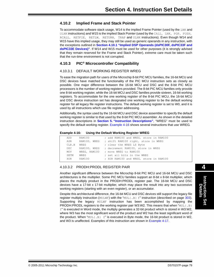
Section 4. Instruction Set DetailsInstruction Set
Details
4
4.10.2 Implied Frame and Stack PointerTo accommodate software stack usage, W14 is the implied Frame Pointer (used by the LNK and ULNK instructions) and W15 is the implied Stack Pointer (used by the CALL, LNK, POP, PUSH, RCALL, RETFIE, RETLW, RETURN, TRAP and ULNK instructions). Even though W14 and W15 have this implied usage, they may still be used as generic operands in any instruction, with the exceptions outlined in Section 4.10.1 “Implied DSP Operands (dsPIC30F, dsPIC33F and dsPIC33E Devices)”. If W14 and W15 must be used for other purposes (it is strongly advised that they remain reserved for the Frame and Stack Pointer), extreme care must be taken such that the run-time environment is not corrupted.
4.10.3 PIC® Microcontroller Compatibility
4.10.3.1 DEFAULT WORKING REGISTER WREG
To ease the migration path for users of the Microchip 8-bit PIC MCU families, the 16-bit MCU and DSC devices have matched the functionality of the PIC MCU instruction sets as closely as possible. One major difference between the 16-bit MCU and DSC and the 8-bit PIC MCU processors is the number of working registers provided. The 8-bit PIC MCU families only provide one 8-bit working register, while the 16-bit MCU and DSC families provide sixteen, 16-bit working registers. To accommodate for the one working register of the 8-bit PIC MCU, the 16-bit MCU and DSC device instruction set has designated one working register to be the default working register for all legacy file register instructions. The default working register is set to W0, and it is used by all instructions which use file register addressing.
Additionally, the syntax used by the 16-bit MCU and DSC device assembler to specify the default working register is similar to that used by the 8-bit PIC MCU assembler. As shown in the detailed instruction descriptions in Section 5. “Instruction Descriptions”, “WREG” must be used to specify the default working register. Example 4-16 shows several instructions that use WREG.
Example 4-16: Using the Default Working Register WREG
4.10.3.2 PRODH:PRODL REGISTER PAIR
Another significant difference between the Microchip 8-bit PIC MCU and 16-bit MCU and DSC architectures is the multiplier. Some PIC MCU families support an 8-bit x 8-bit multiplier, which places the multiply product in the PRODH:PRODL register pair. The 16-bit MCU and DSC devices have a 17-bit x 17-bit multiplier, which may place the result into any two successive working registers (starting with an even register), or an accumulator.
Despite this architectural difference, the 16-bit MCU and DSC devices still support the legacy file register multiply instruction (MULWF) with the “MUL{.B} f” instruction (described on page 303). Supporting the legacy MULWF instruction has been accomplished by mapping the PRODH:PRODL registers to the working register pair W3:W2. This means that when “MUL{.B}f” is executed in Word mode, the multiply generates a 32-bit product which is stored in W3:W2, where W3 has the most significant word of the product and W2 has the least significant word of the product. When “MUL{.B} f” is executed in Byte mode, the 16-bit product is stored in W2, and W3 is unaffected. Examples of this instruction are shown in Example 4-17.
ADD RAM100 ; add RAM100 and WREG, store in RAM100ASR RAM100, WREG ; shift RAM100 right, store in WREGCLR.B WREG ; clear the WREG LS ByteDEC RAM100, WREG ; decrement RAM100, store in WREGMOV WREG, RAM100 ; move WREG to RAM100SETM WREG ; set all bits in the WREGXOR RAM100 ; XOR RAM100 and WREG, store in RAM100
© 2005-2011 Microchip Technology Inc. DS70157F-page 79

16-bit MCU and DSC Programmer’s Reference Manual
Example 4-17: Unsigned f and WREG Multiply (Legacy MULWF Instruction)
4.10.3.3 MOVING DATA WITH WREG
The “MOV{.B} f {,WREG}” instruction (described on page 279) and “MOV{.B} WREG, f” instruction (described on page 280) allow for byte or word data to be moved between file register memory and the WREG (working register W0). These instructions provide equivalent functionality to the legacy Microchip PIC MCU MOVF and MOVWF instructions.
The “MOV{.B} f {,WREG}” and “MOV{.B} WREG, f” instructions are the only MOV instructions which support moves of byte data to and from file register memory. Example 4-18 shows several MOV instruction examples using the WREG.
Example 4-18: Moving Data with WREG
MUL.B 0x100 ; (0x100)*WREG (byte mode), store to W2
Before Instruction:W0 (WREG) = 0x7705W2 = 0x1235W3 = 0x1000Data Memory 0x0100 = 0x1255
After Instruction:W0 (WREG) = 0x7705W2 = 0x01A9W3 = 0x1000Data Memory 0x0100 = 0x1255
MUL 0x100 ; (0x100)*WREG (word mode), store to W3:W2
Before Instruction:W0 (WREG) = 0x7705W2 = 0x1235W3 = 0x1000Data Memory 0x0100 = 0x1255
After Instruction:W0 (WREG) = 0x7705W2 = 0xDEA9W3 = 0x0885Data Memory 0x0100 = 0x1255
Note: When moving word data between file register memory and the working register array, the “MOV Wns, f” and “MOV f, Wnd” instructions allow any working register (W0:W15) to be used as the source or destination register, not just WREG.
MOV.B 0x1001, WREG ; move the byte stored at location 0x1001 to W0MOV 0x1000, WREG ; move the word stored at location 0x1000 to W0MOV.B WREG, TBLPAG ; move the byte stored at W0 to the TBLPAG registerMOV WREG, 0x804 ; move the word stored at W0 to location 0x804
DS70157F-page 80 © 2005-2011 Microchip Technology Inc.

Section 4. Instruction Set DetailsInstruction Set
Details
4
4.11 DSP DATA FORMATS (dsPIC30F, dsPIC33F AND dsPIC33E DEVICES)
4.11.1 Integer and Fractional DataThe dsPIC30F, dsPIC33F, and dsPIC33E devices support both integer and fractional data types. Integer data is inherently represented as a signed two’s complement value, where the Most Significant bit is defined as a sign bit. Generally speaking, the range of an N-bit two’s complement integer is -2N-1 to 2N-1 – 1. For a 16-bit integer, the data range is -32768 (0x8000) to 32767 (0x7FFF), including ‘0’. For a 32-bit integer, the data range is -2,147,483,648 (0x8000 0000) to 2,147,483,647 (0x7FFF FFFF).
Fractional data is represented as a two’s complement number, where the Most Significant bit is defined as a sign bit, and the radix point is implied to lie just after the sign bit. This format is commonly referred to as 1.15 (or Q15) format, where 1 is the number of bits used to represent the integer portion of the number, and 15 is the number of bits used to represent the fractional portion. The range of an N-bit two’s complement fraction with this implied radix point is -1.0 to (1 – 21-N). For a 16-bit fraction, the 1.15 data range is -1.0 (0x8000) to 0.999969482 (0x7FFF), including 0.0 and it has a precision of 3.05176x10⁻⁵. In Normal Saturation mode, the 32-bit accumulators use a 1.31 format, which enhances the precision to 4.6566x10⁻¹⁰.
The dynamic range of the accumulators can be expanded by using the 8 bits of the Upper Accumulator register (ACCxU) as guard bits. Guard bits are used if the value stored in the accumulator overflows beyond the 32nd bit, and they are useful for implementing DSP algorithms. This mode is enabled when the ACCSAT bit (CORCON<4>) is set to ‘1’ and it expands the accumulators to 40 bits. The guard bits are also used when the accumulator saturation is disabled. The accumulators then support an integer range of -5.498x10¹¹ (0x80 0000 0000) to 5.498x10¹¹ (0x7F FFFF FFFF). In Fractional mode, the guard bits of the accumulator do not modify the location of the radix point and the 40-bit accumulators use a 9.31 fractional format. Note that all fractional operation results are stored in the 40-bit Accumulator, justified with a 1.31 radix point. As in Integer mode, the guard bits merely increase the dynamic range of the accumulator. 9.31 fractions have a range of -256.0 (0x80 0000 0000) to (256.0 – 4.65661x10⁻¹⁰) (0x7F FFFF FFFF). Table 4-10 identifies the range and precision of integers and fractions on the dsPIC30F/33F/33E devices for 16-bit, 32-bit and 40-bit registers.
It should be noted that, with the exception of DSP multiplies, the ALU operates identically on integer and fractional data. Namely, an addition of two integers will yield the same result (binary number) as the addition of two fractional numbers. The only difference is how the result is interpreted by the user. However, multiplies performed by DSP operations are different. In these instructions, data format selection is made by the IF bit (CORCON<0>), and it must be set accordingly (‘0’ for Fractional mode, ‘1’ for Integer mode). This is required because of the implied radix point used by dsPIC30F/33F/33E fractional numbers. In Integer mode, multiplying two 16-bit integers produces a 32-bit integer result. However, multiplying two 1.15 values generates a 2.30 result. Since the dsPIC30F, dsPIC33F, and dsPIC33E devices use a 1.31 format for the accumulators, a DSP multiply in Fractional mode also includes a left shift of one bit to keep the radix point properly aligned. This feature reduces the resolution of the DSP multiplier to 2-30, but has no other effect on the computation (e.g., 0.5 x 0.5 = 0.25).
Table 4-10: dsPIC30F/33F/33E Data Ranges
Register Size Integer Range Fraction Range Fraction Resolution
16-bit -32768 to 32767 -1.0 to (1.0 – 2-15) 3.052 x 10⁻⁵
32-bit -2,147,483,648 to 2,147,483,647
-1.0 to (1.0 – 2-31) 4.657 x 10⁻¹⁰
40-bit -549,755,813,888 to 549,755,813,887
-256.0 to (256.0 – 2-31) 4.657 x 10⁻¹⁰
© 2005-2011 Microchip Technology Inc. DS70157F-page 81
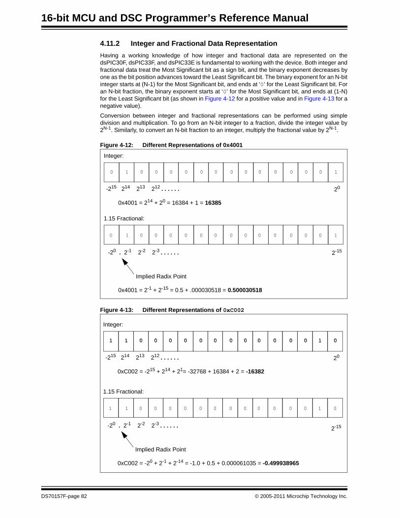
16-bit MCU and DSC Programmer’s Reference Manual
4.11.2 Integer and Fractional Data RepresentationHaving a working knowledge of how integer and fractional data are represented on the dsPIC30F, dsPIC33F, and dsPIC33E is fundamental to working with the device. Both integer and fractional data treat the Most Significant bit as a sign bit, and the binary exponent decreases by one as the bit position advances toward the Least Significant bit. The binary exponent for an N-bit integer starts at (N-1) for the Most Significant bit, and ends at ‘0’ for the Least Significant bit. For an N-bit fraction, the binary exponent starts at ‘0’ for the Most Significant bit, and ends at (1-N) for the Least Significant bit (as shown in Figure 4-12 for a positive value and in Figure 4-13 for a negative value).
Conversion between integer and fractional representations can be performed using simple division and multiplication. To go from an N-bit integer to a fraction, divide the integer value by 2N-1. Similarly, to convert an N-bit fraction to an integer, multiply the fractional value by 2N-1.
Figure 4-12: Different Representations of 0x4001
Figure 4-13: Different Representations of 0xC002
Integer:
1.15 Fractional:
0x4001 = 214 + 20 = 16384 + 1 = 16385
0x4001 = 2-1 + 2-15 = 0.5 + .000030518 = 0.500030518
Implied Radix Point
0 1 0 0 0000 00 0 00 0 0 1
10 0 0 0000 00 0 00 0 0 1
-215 214 213 212 . . . . . . 20
2-15 -20 . 2-1 2-2 2-3 . . . . . .
Integer:
1.15 Fractional:
0xC002 = -215 + 214 + 21= -32768 + 16384 + 2 = -16382
0xC002 = -20 + 2-1 + 2-14 = -1.0 + 0.5 + 0.000061035 = -0.499938965
Implied Radix Point
1 1 0 0 0000 10 0 00 0 0 0
11 0 0 0000 10 0 00 0 0 0
-215 214 213 212 . . . . . . 20
2-15 -20 . 2-1 2-2 2-3 . . . . . .
1 1 0 0 0000 10 0 00 0 0 0
DS70157F-page 82 © 2005-2011 Microchip Technology Inc.

Section 4. Instruction Set DetailsInstruction Set
Details
4
4.12 ACCUMULATOR USAGE (dsPIC30F, dsPIC33F AND dsPIC33E DEVICES)Accumulators A and B are utilized by DSP instructions to perform mathematical and shifting operations. Since the accumulators are 40 bits wide and the X and Y data paths are only 16 bits, the method to load and store the accumulators must be understood.
Item A in Figure 4-14 shows that each 40-bit Accumulator (ACCA and ACCB) consists of an 8-bit Upper register (ACCxU), a 16-bit High register (ACCxH) and a 16-bit Low register (ACCxL). To address the bus alignment requirement and provide the ability for 1.31 math, ACCxH is used as a destination register for loading the accumulator (with the LAC instruction), and also as a source register for storing the accumulator (with the SAC.R instruction). This is represented by Item B, Figure 4-14, where the upper and lower portions of the accumulator are shaded. In reality, during accumulator loads, ACCxL is zero backfilled and ACCxU is sign-extended to represent the sign of the value loaded in ACCxH.
When Normal (31-bit) Saturation is enabled, DSP operations (such as ADD, MAC, MSC, etc.) utilize solely ACCxH:ACCxL (Item C in Figure 4-14) and ACCxU is only used to maintain the sign of the value stored in ACCxH:ACCxL. For instance, when a MPY instruction is executed, the result is stored in ACCxH:ACCxL, and the sign of the result is extended through ACCxU.
When Super Saturation is enabled, or when saturation is disabled, all registers of the accumulator may be used (Item D in Figure 4-14) and the results of DSP operations are stored in ACCxU:ACCxH:ACCxL. The benefit of ACCxU is that it increases the dynamic range of the accumulator, as described in Section 4.11.1 “Integer and Fractional Data”. Refer to Table 4-10 to see the range of values which may be stored in the accumulator when in Normal and Super Saturation modes.
Figure 4-14: Accumulator Alignment and Usage
A)
D)
C)
B)
ACCxU ACCxH ACCxL
A) 40-bit Accumulator consists of ACCxU:ACCxH:ACCxLB) Load and Store operationsC) Operations in Normal Saturation modeD) Operations in Super Saturation mode or with saturation disabled
31.30
Implied Radix Point (between bits 31 and 30)
015163239
© 2005-2011 Microchip Technology Inc. DS70157F-page 83
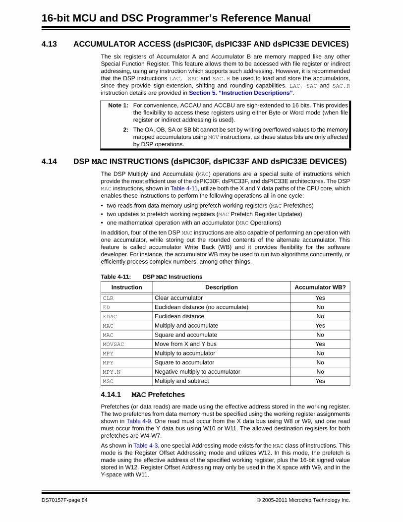
16-bit MCU and DSC Programmer’s Reference Manual
4.13 ACCUMULATOR ACCESS (dsPIC30F, dsPIC33F AND dsPIC33E DEVICES)The six registers of Accumulator A and Accumulator B are memory mapped like any other Special Function Register. This feature allows them to be accessed with file register or indirect addressing, using any instruction which supports such addressing. However, it is recommended that the DSP instructions LAC, SAC and SAC.R be used to load and store the accumulators, since they provide sign-extension, shifting and rounding capabilities. LAC, SAC and SAC.Rinstruction details are provided in Section 5. “Instruction Descriptions”.
4.14 DSP MAC INSTRUCTIONS (dsPIC30F, dsPIC33F AND dsPIC33E DEVICES)The DSP Multiply and Accumulate (MAC) operations are a special suite of instructions which provide the most efficient use of the dsPIC30F, dsPIC33F, and dsPIC33E architectures. The DSP MAC instructions, shown in Table 4-11, utilize both the X and Y data paths of the CPU core, which enables these instructions to perform the following operations all in one cycle:
• two reads from data memory using prefetch working registers (MAC Prefetches)• two updates to prefetch working registers (MAC Prefetch Register Updates)• one mathematical operation with an accumulator (MAC Operations)
In addition, four of the ten DSP MAC instructions are also capable of performing an operation with one accumulator, while storing out the rounded contents of the alternate accumulator. This feature is called accumulator Write Back (WB) and it provides flexibility for the software developer. For instance, the accumulator WB may be used to run two algorithms concurrently, or efficiently process complex numbers, among other things.
Table 4-11: DSP MAC Instructions
4.14.1 MAC PrefetchesPrefetches (or data reads) are made using the effective address stored in the working register. The two prefetches from data memory must be specified using the working register assignments shown in Table 4-9. One read must occur from the X data bus using W8 or W9, and one read must occur from the Y data bus using W10 or W11. The allowed destination registers for both prefetches are W4-W7.
As shown in Table 4-3, one special Addressing mode exists for the MAC class of instructions. This mode is the Register Offset Addressing mode and utilizes W12. In this mode, the prefetch is made using the effective address of the specified working register, plus the 16-bit signed value stored in W12. Register Offset Addressing may only be used in the X space with W9, and in the Y-space with W11.
Note 1: For convenience, ACCAU and ACCBU are sign-extended to 16 bits. This provides the flexibility to access these registers using either Byte or Word mode (when file register or indirect addressing is used).
2: The OA, OB, SA or SB bit cannot be set by writing overflowed values to the memory mapped accumulators using MOV instructions, as these status bits are only affected by DSP operations.
Instruction Description Accumulator WB?
CLR Clear accumulator YesED Euclidean distance (no accumulate) NoEDAC Euclidean distance NoMAC Multiply and accumulate YesMAC Square and accumulate NoMOVSAC Move from X and Y bus YesMPY Multiply to accumulator NoMPY Square to accumulator NoMPY.N Negative multiply to accumulator NoMSC Multiply and subtract Yes
DS70157F-page 84 © 2005-2011 Microchip Technology Inc.

Section 4. Instruction Set DetailsInstruction Set
Details
4
4.14.2 MAC Prefetch Register UpdatesAfter the MAC prefetches are made, the effective address stored in each prefetch working register may be modified. This feature enables efficient single-cycle processing for data stored sequentially in X and Y memory. Since all DSP instructions execute in Word mode, only even numbered updates may be made to the effective address stored in the working register. Allowable address modifications to each prefetch register are -6, -4, -2, 0 (no update), +2, +4 and +6. This means that effective address updates may be made up to 3 words in either direction.
When the Register Offset Addressing mode is used, no update is made to the base prefetch register (W9 or W11), or the offset register (W12).
4.14.3 MAC OperationsThe mathematical operations performed by the MAC class of DSP instructions center around multiplying the contents of two working registers and either adding or storing the result to either Accumulator A or Accumulator B. This is the operation of the MAC, MPY, MPY.N and MSCinstructions. Table 4-9 shows that W4-W7 must be used for data source operands in the MACclass of instructions. W4-W7 may be combined in any fashion, and when the same working register is specified for both operands, a square or square and accumulate operation is performed.
For the ED and EDAC instructions, the same multiplicand operand must be specified by the instruction, because this is the definition of the Euclidean Distance operation. Another unique feature about this instruction is that the values prefetched from X and Y memory are not actually stored in W4-W7. Instead, only the difference of the prefetched data words is stored in W4-W7.
The two remaining MAC class instructions, CLR and MOVSAC, are useful for initiating or completing a series of MAC or EDAC instructions and do not use the multiplier. CLR has the ability to clear Accumulator A or B, prefetch two values from data memory and store the contents of the other accumulator. Similarly, MOVSAC has the ability to prefetch two values from data memory and store the contents of either accumulator.
4.14.4 MAC Write BackThe write back ability of the MAC class of DSP instructions facilitates efficient processing of algorithms. This feature allows one mathematical operation to be performed with one accumulator, and the rounded contents of the other accumulator to be stored in the same cycle. As indicated in Table 4-9, register W13 is assigned for performing the write back, and two Addressing modes are supported: Direct and Indirect with Post-Increment.
The CLR, MOVSAC and MSC instructions support accumulator Write Back, while the ED, EDAC, MPY and MPY.N instructions do not support accumulator Write Back. The MAC instruction, which multiplies two working registers which are not the same, also supports accumulator Write Back. However, the square and accumulate MAC instruction does not support accumulator Write Back (see Table 4-11).
4.14.5 MAC SyntaxThe syntax of the MAC class of instructions can have several formats, which depend on the instruction type and the operation it is performing, with respect to prefetches and accumulator Write Back. With the exception of the CLR and MOVSAC instructions, all MAC class instructions must specify a target accumulator along with two multiplicands, as shown in Example 4-19.
Example 4-19: Base MAC Syntax
Multiply W7*W7, Accumulate to ACCB
; MAC with no prefetchMAC W4*W5, A
; MAC with no prefetchMAC W7*W7, B
© 2005-2011 Microchip Technology Inc. DS70157F-page 85
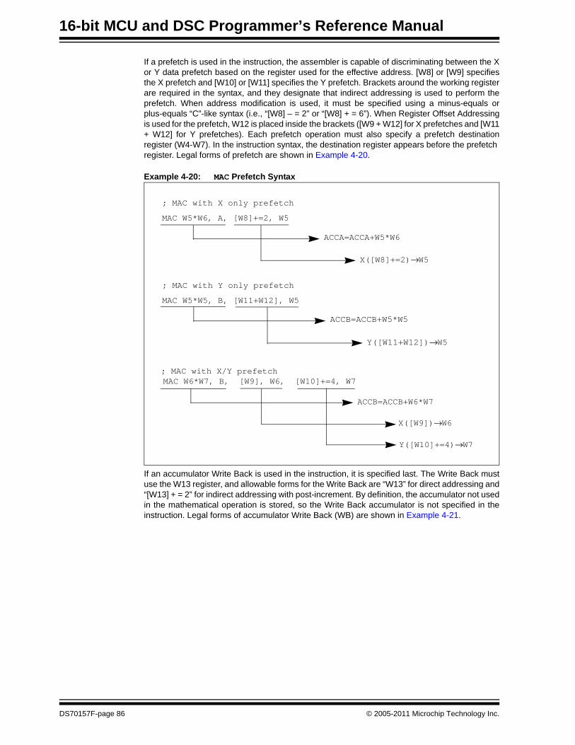
16-bit MCU and DSC Programmer’s Reference Manual
If a prefetch is used in the instruction, the assembler is capable of discriminating between the X or Y data prefetch based on the register used for the effective address. [W8] or [W9] specifies the X prefetch and [W10] or [W11] specifies the Y prefetch. Brackets around the working register are required in the syntax, and they designate that indirect addressing is used to perform the prefetch. When address modification is used, it must be specified using a minus-equals or plus-equals “C”-like syntax (i.e., “[W8] – = 2” or “[W8] + = 6”). When Register Offset Addressing is used for the prefetch, W12 is placed inside the brackets ([W9 + W12] for X prefetches and [W11 + W12] for Y prefetches). Each prefetch operation must also specify a prefetch destination register (W4-W7). In the instruction syntax, the destination register appears before the prefetch register. Legal forms of prefetch are shown in Example 4-20.
Example 4-20: MAC Prefetch Syntax
If an accumulator Write Back is used in the instruction, it is specified last. The Write Back must use the W13 register, and allowable forms for the Write Back are “W13” for direct addressing and “[W13] + = 2” for indirect addressing with post-increment. By definition, the accumulator not used in the mathematical operation is stored, so the Write Back accumulator is not specified in the instruction. Legal forms of accumulator Write Back (WB) are shown in Example 4-21.
X([W8]+=2)→ W5
ACCA=ACCA+W5*W6
; MAC with X only prefetch
MAC W5*W6, A, [W8]+=2, W5
Y([W11+W12])→ W5
ACCB=ACCB+W5*W5
; MAC with Y only prefetch
MAC W5*W5, B, [W11+W12], W5
X([W9])→ W6
ACCB=ACCB+W6*W7
Y([W10]+=4)→ W7
; MAC with X/Y prefetchMAC W6*W7, B, [W9], W6, [W10]+=4, W7
DS70157F-page 86 © 2005-2011 Microchip Technology Inc.

Section 4. Instruction Set DetailsInstruction Set
Details
4
Example 4-21: MAC Accumulator WB Syntax
Putting it all together, an MSC instruction which performs two prefetches and a write back is shown in Example 4-22.
Example 4-22: MSC Instruction with Two Prefetches and Accumulator Write Back
ACCB → W13
0 → ACCA
; CLR with direct WB of ACCB
CLR A, W13
ACCB → [W13]+=2
ACCA=ACCA+W4*W5
; MAC with indirect WB of ACCB
MAC W4*W5, A [W13]+=2
Y([W10]+=2)→ W4
ACCB=ACCB+W4*W5
ACCA → W13
; MAC with Y prefetch, direct WB of ACCA
MAC W4*W5, B, [W10]+=2, W4, W13
ACCB=ACCB-W6*W7
X([W8]+=2)→W6Y([W10]-=6)→W7
ACCA→[W13]+=2
; MSC with X/Y prefetch, indirect WB of ACCA
MSC W6*W7, B, [W8]+=2, W6, [W10]-=6, W7 [W13]+=2
© 2005-2011 Microchip Technology Inc. DS70157F-page 87

16-bit MCU and DSC Programmer’s Reference Manual
4.15 DSP ACCUMULATOR INSTRUCTIONS (dsPIC30F, dsPIC33F AND dsPIC33E DEVICES)
The DSP Accumulator instructions do not have prefetch or accumulator WB ability, but they do provide the ability to add, negate, shift, load and store the contents of either 40-bit Accumulator. In addition, the ADD and SUB instructions allow the two accumulators to be added or subtracted from each other. DSP Accumulator instructions are shown in Table 4-12 and instruction details are provided in Section 5. “Instruction Descriptions”.
Table 4-12: DSP Accumulator Instructions
4.16 SCALING DATA WITH THE FBCL INSTRUCTION (dsPIC30F, dsPIC33F AND dsPIC33E DEVICES)
To minimize quantization errors that are associated with data processing using DSP instructions, it is important to utilize the complete numerical result of the operations. This may require scaling data up to avoid underflow (i.e., when processing data from a 12-bit ADC), or scaling data down to avoid overflow (i.e., when sending data to a 10-bit DAC). The scaling, which must be performed to minimize quantization error, depends on the dynamic range of the input data which is operated on, and the required dynamic range of the output data. At times, these conditions may be known beforehand and fixed scaling may be employed. In other cases, scaling conditions may not be fixed or known, and then dynamic scaling must be used to process data.
The FBCL instruction (Find First Bit Change Left) can efficiently be used to perform dynamic scaling, because it determines the exponent of a value. A fixed point or integer value’s exponent represents the amount which the value may be shifted before overflowing. This information is valuable, because it may be used to bring the data value to “full scale”, meaning that its numeric representation utilizes all the bits of the register it is stored in.
The FBCL instruction determines the exponent of a word by detecting the first bit change starting from the value’s sign bit and working towards the LSB. Since the dsPIC DSC device’s barrel shifter uses negative values to specify a left shift, the FBCL instruction returns the negated exponent of a value. If the value is being scaled up, this allows the ensuing shift to be performed immediately with the value returned by FBCL. Additionally, since the FBCL instruction only operates on signed quantities, FBCL produces results in the range of -15:0. When the FBCLinstruction returns ‘0’, it indicates that the value is already at full scale. When the instruction returns -15, it indicates that the value cannot be scaled (as is the case with 0x0 and 0xFFFF). Table 4-13 shows word data with various dynamic ranges, their exponents, and the value after scaling each data to maximize the dynamic range. Example 4-23 shows how the FBCLinstruction may be used for block processing.
Instruction Description Accumulator WB?
ADD Add accumulators NoADD 16-bit signed accumulator add NoLAC Load accumulator NoNEG Negate accumulator NoSAC Store accumulator NoSAC.R Store rounded accumulator NoSFTAC Arithmetic shift accumulator by Literal NoSFTAC Arithmetic shift accumulator by (Wn) NoSUB Subtract accumulators No
DS70157F-page 88 © 2005-2011 Microchip Technology Inc.

Section 4. Instruction Set DetailsInstruction Set
Details
4
Table 4-13: Scaling Examples
As a practical example, assume that block processing is performed on a sequence of data with very low dynamic range stored in 1.15 fractional format. To minimize quantization errors, the data may be scaled up to prevent any quantization loss which may occur as it is processed. The FBCLinstruction can be executed on the sample with the largest magnitude to determine the optimal scaling value for processing the data. Note that scaling the data up is performed by left shifting the data. This is demonstrated with the code snippet below.
Example 4-23: Scaling with FBCL
Word Value Exponent Full Scale Value(Word Value << Exponent)
0x0001 14 0x40000x0002 13 0x40000x0004 12 0x40000x0100 6 0x40000x01FF 6 0x7FC00x0806 3 0x40300x2007 1 0x400E0x4800 0 0x48000x7000 0 0x70000x8000 0 0x80000x900A 0 0x900A0xE001 2 0x80040xFF07 7 0x8380
Note: For the word values 0x0000 and 0xFFFF, the FBCL instruction returns -15.
; assume W0 contains the largest absolute value of the data block; assume W4 points to the beginning of the data block; assume the block of data contains BLOCK_SIZE words
; determine the exponent to use for scalingFBCL W0, W2 ; store exponent in W2
; scale the entire data block before processingDO #(BLOCK_SIZE-1), SCALELAC [W4], A ; move the next data sample to ACCASFTAC A, W2 ; shift ACCA by W2 bits
SCALE: SAC A, [W4++] ; store scaled input (overwrite original)
; now process the data; (processing block goes here)
© 2005-2011 Microchip Technology Inc. DS70157F-page 89
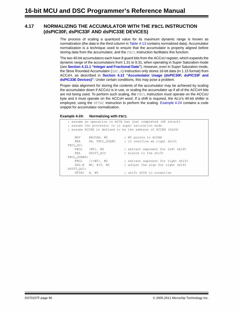
16-bit MCU and DSC Programmer’s Reference Manual
4.17 NORMALIZING THE ACCUMULATOR WITH THE FBCL INSTRUCTION (dsPIC30F, dsPIC33F AND dsPIC33E DEVICES)
The process of scaling a quantized value for its maximum dynamic range is known as normalization (the data in the third column in Table 4-13 contains normalized data). Accumulator normalization is a technique used to ensure that the accumulator is properly aligned before storing data from the accumulator, and the FBCL instruction facilitates this function.
The two 40-bit accumulators each have 8 guard bits from the ACCxU register, which expands the dynamic range of the accumulators from 1.31 to 9.31, when operating in Super Saturation mode (see Section 4.11.1 “Integer and Fractional Data”). However, even in Super Saturation mode, the Store Rounded Accumulator (SAC.R) instruction only stores 16-bit data (in 1.15 format) from ACCxH, as described in Section 4.12 “Accumulator Usage (dsPIC30F, dsPIC33F and dsPIC33E Devices)”. Under certain conditions, this may pose a problem.
Proper data alignment for storing the contents of the accumulator may be achieved by scaling the accumulator down if ACCxU is in use, or scaling the accumulator up if all of the ACCxH bits are not being used. To perform such scaling, the FBCL instruction must operate on the ACCxU byte and it must operate on the ACCxH word. If a shift is required, the ALU’s 40-bit shifter is employed, using the SFTAC instruction to perform the scaling. Example 4-24 contains a code snippet for accumulator normalization.
Example 4-24: Normalizing with FBCL; assume an operation in ACCA has just completed (SR intact); assume the processor is in super saturation mode; assume ACCAH is defined to be the address of ACCAH (0x24)
MOV #ACCAH, W5 ; W5 points to ACCAHBRA OA, FBCL_GUARD ; if overflow we right shift
FBCL_HI:FBCL [W5], W0 ; extract exponent for left shiftBRA SHIFT_ACC ; branch to the shift
FBCL_GUARD:FBCL [++W5], W0 ; extract exponent for right shiftADD.B W0, #15, W0 ; adjust the sign for right shift
SHIFT_ACC:SFTAC A, W0 ; shift ACCA to normalize
DS70157F-page 90 © 2005-2011 Microchip Technology Inc.

Section 4. Instruction Set DetailsInstruction Set
Details
4
4.18 EXTENDED-PRECISON ARITHMETIC USING MIXED-SIGN MULTIPLICATIONS (dsPIC33E ONLY)
Many DSP algorithms utilize extended-precision arithmetic operations (operations with 32-bit or 64-bit operands and results) to enhance the resolution and accuracy of computations. These can be implemented using 16-bit signed or unsigned multiplications; however, this would require some additional processing and shifting of the data to obtain the correct results. To enable such extended-precision algorithms to be computed faster, dsPIC33E devices support an optional implicit mixed-sign multiplication mode, which is selected by setting US<1:0> (CORCON<13:12>) = '10'.
In this mode, mixed-sign (unsigned x signed and signed x unsigned) multiplications can be performed without the need to dynamically reconfigure the US<1:0> bits and shift data to account for the difference in operand formats. Moreover, signed x signed and unsigned x unsigned multiplications can also be performed without changing the multiplication mode. Each input operand is implicitly treated as an unsigned number if the working register being used to specify the operand is either W4 or W6. Similarly, an operand is treated as a signed number if the register used is either W5 or W7. The DSP Engine selects the type of multiplication to be performed based on the operand registers used, thereby eliminating the need for the user software to modify the US<1:0> bits.
The execution time reductions provided by the implicit mixed-sign multiplication feature is illustrated in the following code example, where the instruction cycle count for performing a 32-bit multiplication is reduced from 7 cycles to 4 cycles when the mixed-sign multiplication mode is enabled.
Example 4-25: 32-bit Signed Multiplication using Implicit Mixed-Sign Mode
Besides DSP instructions, MCU multiplication (MUL) instructions can also utilize Accumulator A or Accumulator B as a result destination, which enables faster extended-precision arithmetic even when not using DSP multiplication instructions such as MPY or MAC.
Case A - Mixed-Sign Multiplication Mode Not EnabledMUL.SU W5, W6, W0; Word1 (signed) x Word2 (unsigned)MUL.US W4, W7, W2; Word0 (unsigned) x Word3 (signed)CLR B ; Clear Accumulator BADD W1, BADD W3, BSFTAC B, #15 ; Shift right by 15 bits to align for Q31 formatMAC W5*W7, B; Word1 (signed) x Word 3 (signed)
Case B - Mixed-Sign Multiplication Mode EnabledMPY W5*W6, B; Word1 (signed) x Word2 (unsigned)MAC W4*W7, B; Word0 (unsigned) x Word3 (signed)SFTAC B, #15 ; Shift right by 15 bits to align for Q31 formatMAC W5*W7, B; Word1 (signed) x Word 3 (signed)
© 2005-2011 Microchip Technology Inc. DS70157F-page 91
16-bit MCU and DSC Programmer’s Reference Manual
DS70157F-page 92 © 2005-2011 Microchip Technology Inc.
Section 5. Instruction Descriptions
Instruction D
escriptions
5
HIGHLIGHTSThis section of the manual contains the following major topics:
5.1 Instruction Symbols......................................................................................................... 945.2 Instruction Encoding Field Descriptors Introduction........................................................ 945.3 Instruction Description Example ..................................................................................... 985.4 Instruction Descriptions................................................................................................... 99
© 2005-2011 Microchip Technology Inc. DS70157F-page 93

16-bit MCU and DSC Programmer’s Reference Manual
5.1 INSTRUCTION SYMBOLSAll the symbols used in Section 5.4 “Instruction Descriptions” are listed in Table 1-2.
5.2 INSTRUCTION ENCODING FIELD DESCRIPTORS INTRODUCTIONAll instruction encoding field descriptors used in Section 5.4 “Instruction Descriptions” are shown in Table 5-2 through Table 5-12.
Table 5-1: Instruction Encoding Field Descriptors Field Description
A(1) Accumulator selection bit: 0 = ACCA; 1 = CCB
aa(1) Accumulator Write Back mode (see Table 5-12)
B Byte mode selection bit: 0 = word operation; 1 = byte operationbbbb 4-bit bit position select: 0000 = LSB; 1111 = MSB
D Destination address bit: 0 = result stored in WREG;1 = result stored in file register
dddd Wd destination register select: 0000 = W0; 1111 = W15f ffff ffff ffff 13-bit register file address (0x0000 to 0x1FFF)
fff ffff ffff ffff 15-bit register file word address (implied 0 LSB)(0x0000 to 0xFFFE)
ffff ffff ffff ffff 16-bit register file byte address (0x0000 to 0xFFFF)ggg Register Offset Addressing mode for Ws source register (see Table 5-4)hhh Register Offset Addressing mode for Wd destination register (see Table 5-5)
iiii(1) Prefetch X Operation (see Table 5-6)
jjjj(1) Prefetch Y Operation (see Table 5-8)
k 1-bit literal field, constant data or expressionkkkk 4-bit literal field, constant data or expression
kk kkkk 6-bit literal field, constant data or expressionkkkk kkkk 8-bit literal field, constant data or expression
kk kkkk kkkk 10-bit literal field, constant data or expressionkk kkkk kkkk kkkk 14-bit literal field, constant data or expression
kkkk kkkk kkkk kkkk 16-bit literal field, constant data or expressionmm Multiplier source select with same working registers (see Table 5-10)mmm Multiplier source select with different working registers (see Table 5-11)
nnnn nnnn nnnn nnn0 nnn nnnn
23-bit program address for CALL and GOTO instructions
nnnn nnnn nnnn nnnn 16-bit program offset field for relative branch/call instructionsppp Addressing mode for Ws source register (see Table 5-2)qqq Addressing mode for Wd destination register (see Table 5-3)
rrrr Barrel shift countssss Ws source register select: 0000 = W0; 1111 = W15tttt Dividend select, most significant wordvvvv Dividend select, least significant word
W Double Word mode selection bit: 0 = word operation;1 = double word operation
wwww Wb base register select: 0000 = W0; 1111 = W15xx(1) Prefetch X Destination (see Table 5-7)
xxxx xxxx xxxx xxxx 16-bit unused field (don’t care)yy(1) Prefetch Y Destination (see Table 5-9)
z Bit test destination: 0 = C flag bit; 1 = Z flag bit Note 1: This field is only available in dsPIC30F, dsPIC33F, and dsPIC33E devices.
DS70157F-page 94 © 2005-2011 Microchip Technology Inc.

Section 5. Instruction DescriptionsInstruction
Descriptions
5
Table 5-2: Addressing Modes for Ws Source Register
Table 5-3: Addressing Modes for Wd Destination Register
Table 5-4: Offset Addressing Modes for Ws Source Register (with Register Offset)
Table 5-5: Offset Addressing Modes for Wd Destination Register (with Register Offset)
ppp Addressing Mode Source Operand
000 Register Direct Ws
001 Indirect [Ws]
010 Indirect with Post-Decrement [Ws--]
011 Indirect with Post-Increment [Ws++]
100 Indirect with Pre-Decrement [--Ws]
101 Indirect with Pre-Increment [++Ws]
11x Unused
qqq Addressing Mode Destination Operand
000 Register Direct Wd
001 Indirect [Wd]
010 Indirect with Post-Decrement [Wd--]
011 Indirect with Post-Increment [Wd++]
100 Indirect with Pre-Decrement [--Wd]
101 Indirect with Pre-Increment [++Wd]
11x Unused (an attempt to use this Addressing mode will force a RESET instruction)
ggg Addressing Mode Source Operand
000 Register Direct Ws
001 Indirect [Ws]
010 Indirect with Post-Decrement [Ws--]
011 Indirect with Post-Increment [Ws++]
100 Indirect with Pre-Decrement [--Ws]
101 Indirect with Pre-Increment [++Ws]
11x Indirect with Register Offset [Ws+Wb]
hhh Addressing Mode Source Operand
000 Register Direct Wd
001 Indirect [Wd]
010 Indirect with Post-Decrement [Wd--]
011 Indirect with Post-Increment [Wd++]
100 Indirect with Pre-Decrement [--Wd]
101 Indirect with Pre-Increment [++Wd]
11x Indirect with Register Offset [Wd+Wb]
© 2005-2011 Microchip Technology Inc. DS70157F-page 95

16-bit MCU and DSC Programmer’s Reference Manual
Table 5-6: X Data Space Prefetch Operation (dsPIC30F, dsPIC33F and dsPIC33E)
Table 5-7: X Data Space Prefetch Destination (dsPIC30F, dsPIC33F and dsPIC33E)
Table 5-8: Y Data Space Prefetch Operation (dsPIC30F, dsPIC33F and dsPIC33E)
iiii Operation0000 Wxd = [W8]0001 Wxd = [W8], W8 = W8 + 20010 Wxd = [W8], W8 = W8 + 40011 Wxd = [W8], W8 = W8 + 60100 No Prefetch for X Data Space0101 Wxd = [W8], W8 = W8 – 60110 Wxd = [W8], W8 = W8 – 40111 Wxd = [W8], W8 = W8 – 21000 Wxd = [W9]1001 Wxd = [W9], W9 = W9 + 21010 Wxd = [W9], W9 = W9 + 41011 Wxd = [W9], W9 = W9 + 61100 Wxd = [W9 + W12]1101 Wxd = [W9], W9 = W9 – 61110 Wxd = [W9], W9 = W9 – 41111 Wxd = [W9], W9 = W9 – 2
xx Wxd
00 W4
01 W5
10 W6
11 W7
jjjj Operation
0000 Wyd = [W10]
0001 Wyd = [W10], W10 = W10 + 2
0010 Wyd = [W10], W10 = W10 + 4
0011 Wyd = [W10], W10 = W10 + 6
0100 No Prefetch for Y Data Space
0101 Wyd = [W10], W10 = W10 – 6
0110 Wyd = [W10], W10 = W10 – 4
0111 Wyd = [W10], W10 = W10 – 2
1000 Wyd = [W11]
1001 Wyd = [W11], W11 = W11 + 2
1010 Wyd = [W11], W11 = W11 + 4
1011 Wyd = [W11], W11 = W11 + 6
1100 Wyd = [W11 + W12]
1101 Wyd = [W11], W11 = W11 – 6
1110 Wyd = [W11], W11 = W11 – 4
1111 Wyd = [W11], W11 = W11 – 2
DS70157F-page 96 © 2005-2011 Microchip Technology Inc.

Section 5. Instruction DescriptionsInstruction
Descriptions
5
Table 5-9: Y Data Space Prefetch Destination (dsPIC30F, dsPIC33F and dsPIC33E)
Table 5-10: MAC or MPY Source Operands (Same Working Register) (dsPIC30F, dsPIC33F and dsPIC33E)
Table 5-11: MAC or MPY Source Operands (Different Working Register) (dsPIC30F, dsPIC33F and dsPIC33E)
Table 5-12: MAC Accumulator Write Back Selection (dsPIC30F, dsPIC33F and dsPIC33E)
Table 5-13: MOVPAG Destination Selection
Table 5-14: Accumulator Selection
yy Wyd00 W401 W510 W611 W7
mm Multiplicands00 W4 * W401 W5 * W510 W6 * W611 W7 * W7
mmm Multiplicands000 W4 * W5001 W4 * W6010 W4 * W7011 Invalid100 W5 * W6101 W5 * W7110 W6 * W7111 Invalid
aa Write Back Selection00 W13 = Other Accumulator (Direct Addressing)01 [W13] + = 2 = Other Accumulator (Indirect Addressing with Post-Increment)10 No Write Back11 Invalid
PP Target Page Register00 DSRPAG
01 DSWPAG
10 TBLPAG
11 Reserved – do not use
A Target Accumulator0 Accumulator A1 Accumulator B
© 2005-2011 Microchip Technology Inc. DS70157F-page 97
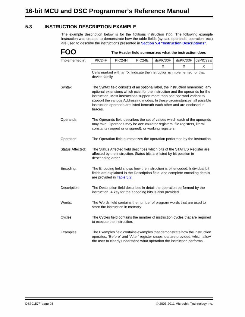
16-bit MCU and DSC Programmer’s Reference Manual
5.3 INSTRUCTION DESCRIPTION EXAMPLEThe example description below is for the fictitious instruction FOO. The following example instruction was created to demonstrate how the table fields (syntax, operands, operation, etc.) are used to describe the instructions presented in Section 5.4 “Instruction Descriptions”.
FOO The Header field summarizes what the instruction does
Implemented in: PIC24F PIC24H PIC24E dsPIC30F dsPIC33F dsPIC33E
X X X
Cells marked with an ‘X’ indicate the instruction is implemented for that device family.
Syntax: The Syntax field consists of an optional label, the instruction mnemonic, any optional extensions which exist for the instruction and the operands for the instruction. Most instructions support more than one operand variant to support the various Addressing modes. In these circumstances, all possible instruction operands are listed beneath each other and are enclosed in braces.
Operands: The Operands field describes the set of values which each of the operands may take. Operands may be accumulator registers, file registers, literal constants (signed or unsigned), or working registers.
Operation: The Operation field summarizes the operation performed by the instruction.
Status Affected: The Status Affected field describes which bits of the STATUS Register are affected by the instruction. Status bits are listed by bit position in descending order.
Encoding: The Encoding field shows how the instruction is bit encoded. Individual bit fields are explained in the Description field, and complete encoding details are provided in Table 5.2.
Description: The Description field describes in detail the operation performed by the instruction. A key for the encoding bits is also provided.
Words: The Words field contains the number of program words that are used to store the instruction in memory.
Cycles: The Cycles field contains the number of instruction cycles that are required to execute the instruction.
Examples: The Examples field contains examples that demonstrate how the instruction operates. “Before” and “After” register snapshots are provided, which allow the user to clearly understand what operation the instruction performs.
DS70157F-page 98 © 2005-2011 Microchip Technology Inc.

Section 5. Instruction DescriptionsInstruction
Descriptions
5
5.4 INSTRUCTION DESCRIPTIONS
ADD Add f to WREG
Implemented in: PIC24F PIC24H PIC24E dsPIC30F dsPIC33F dsPIC33E
X X X X X X
Syntax: {label:} ADD{.B} f {,WREG}
Operands: f ∈ [0 ... 8191]
Operation: (f) + (WREG) → destination designated by D
Status Affected: DC, N, OV, Z, C
Encoding: 1011 0100 0BDf ffff ffff ffff
Description: Add the contents of the default working register WREG to the contents of the file register, and place the result in the destination register. The optional WREG operand determines the destination register. If WREG is specified, the result is stored in WREG. If WREG is not specified, the result is stored in the file register.
The ‘B’ bit selects byte or word operation (‘0’ for word, ‘1’ for byte).The ‘D’ bit selects the destination (‘0’ for WREG, ‘1’ for file register).The ‘f’ bits select the address of the file register.
Note 1: The extension .B in the instruction denotes a byte operation rather than a word operation. You may use a .W extension to denote a word operation, but it is not required.
2: The WREG is set to working register W0.
Words: 1
Cycles: 1(1)
Note 1: In dsPIC33E and PIC24E devices, the listed cycle count does not apply to read and read-modify-write operations on non-CPU Special Function Registers. For more details, see Note 3 in Section 3.2.1 “Multi-Cycle Instructions”.
Example 1: ADD.B RAM100 ; Add WREG to RAM100 (Byte mode)
Before Instruction
AfterInstruction
WREG CC80 WREG CC80 RAM100 FFC0 RAM100 FF40
SR 0000 SR 0005 (OV, C = 1)
Example 2: ADD RAM200, WREG ; Add RAM200 to WREG (Word mode)
Before Instruction
AfterInstruction
WREG CC80 WREG CC40 RAM200 FFC0 RAM200 FFC0
SR 0000 SR 0001 (C = 1)
© 2005-2011 Microchip Technology Inc. DS70157F-page 99

16-bit MCU and DSC Programmer’s Reference Manual
ADD Add Literal to Wn
Implemented in: PIC24F PIC24H PIC24E dsPIC30F dsPIC33F dsPIC33E
X X X X X X
Syntax: {label:} ADD{.B} #lit10, Wn
Operands: lit10 ∈ [0 ... 255] for byte operationlit10 ∈ [0 ... 1023] for word operationWn ∈ [W0 ... W15]
Operation: lit10 + (Wn) → Wn
Status Affected: DC, N, OV, Z, C
Encoding: 1011 0000 0Bkk kkkk kkkk dddd
Description: Add the 10-bit unsigned literal operand to the contents of the working register Wn, and place the result back into the working register Wn.
The ‘B’ bit selects byte or word operation (‘0’ for word, ‘1’ for byte).The ‘k’ bits specify the literal operand.The ‘d’ bits select the address of the working register.
Note 1: The extension .B in the instruction denotes a byte operation rather than a word operation. You may use a .W extension to denote a word operation, but it is not required.
2: For byte operations, the literal must be specified as an unsigned value [0:255]. See Section 4.6 “Using 10-bit Literal Operands” for information on using 10-bit literal operands in Byte mode.
Words: 1
Cycles: 1
Example 1: ADD.B #0xFF, W7 ; Add -1 to W7 (Byte mode)
Before Instruction
AfterInstruction
W7 12C0 W7 12BFSR 0000 SR 0009 (N, C = 1)
Example 2: ADD #0xFF, W1 ; Add 255 to W1 (Word mode)
Before Instruction
AfterInstruction
W1 12C0 W1 13BFSR 0000 SR 0000
DS70157F-page 100 © 2005-2011 Microchip Technology Inc.
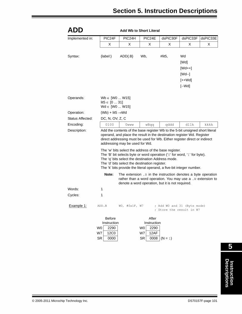
Section 5. Instruction DescriptionsInstruction
Descriptions
5
ADD Add Wb to Short Literal
Implemented in: PIC24F PIC24H PIC24E dsPIC30F dsPIC33F dsPIC33E
X X X X X X
Syntax: {label:} ADD{.B} Wb, #lit5, Wd
[Wd]
[Wd++]
[Wd--]
[++Wd]
[--Wd]
Operands: Wb ∈ [W0 ... W15]lit5 ∈ [0 ... 31]Wd ∈ [W0 ... W15]
Operation: (Wb) + lit5 → Wd
Status Affected: DC, N, OV, Z, C
Encoding: 0100 0www wBqq qddd d11k kkkk
Description: Add the contents of the base register Wb to the 5-bit unsigned short literal operand, and place the result in the destination register Wd. Register direct addressing must be used for Wb. Either register direct or indirect addressing may be used for Wd.
The ‘w’ bits select the address of the base register.The ‘B’ bit selects byte or word operation (‘0’ for word, ‘1’ for byte).The ‘q’ bits select the destination Address mode.The ‘d’ bits select the destination register.The ‘k’ bits provide the literal operand, a five-bit integer number.
Note: The extension .B in the instruction denotes a byte operation rather than a word operation. You may use a .W extension to denote a word operation, but it is not required.
Words: 1
Cycles: 1
Example 1: ADD.B W0, #0x1F, W7 ; Add W0 and 31 (Byte mode); Store the result in W7
Before Instruction
AfterInstruction
W0 2290 W0 2290W7 12C0 W7 12AFSR 0000 SR 0008 (N = 1)
© 2005-2011 Microchip Technology Inc. DS70157F-page 101

16-bit MCU and DSC Programmer’s Reference Manual
Example 2: ADD W3, #0x6, [--W4] ; Add W3 and 6 (Word mode); Store the result in [--W4]
Before Instruction
AfterInstruction
W3 6006 W3 6006W4 1000 W4 0FFE
Data 0FFE DDEE Data 0FFE 600CData 1000 DDEE Data 1000 DDEE
SR 0000 SR 0000
ADD Add Wb to Ws
Implemented in: PIC24F PIC24H PIC24E dsPIC30F dsPIC33F dsPIC33E
X X X X X X
Syntax: {label:} ADD{.B} Wb, Ws, Wd
[Ws], [Wd]
[Ws++], [Wd++]
[Ws--], [Wd--]
[++Ws], [++Wd]
[--Ws], [--Wd]
Operands: Wb ∈ [W0 ... W15]Ws ∈ [W0 ... W15]Wd ∈ [W0 ... W15]
Operation: (Wb) + (Ws) → Wd
Status Affected: DC, N, OV, Z, C
Encoding: 0100 0www wBqq qddd dppp ssss
Description: Add the contents of the source register Ws and the contents of the base register Wb, and place the result in the destination register Wd. Register direct addressing must be used for Wb. Either register direct or indirect addressing may be used for Ws and Wd.
The ‘w’ bits select the address of the base register.The ‘B’ bit selects byte or word operation (‘0’ for word, ‘1’ for byte).The ‘q’ bits select the destination Address mode.The ‘d’ bits select the destination register.The ‘p’ bits select the source Address mode.The ‘s’ bits select the source register.
Note: The extension .B in the instruction denotes a byte operation rathjer than a word operation. You may use a .W extension to denote a word operation, but it is not required.
Words: 1
Cycles: 1(1)
Note 1: In dsPIC33E and PIC24E devices, the listed cycle count does not apply to read and read-modify-write operations on non-CPU Special Function Registers. For more details, see Note 3 in Section 3.2.1 “Multi-Cycle Instructions”.
DS70157F-page 102 © 2005-2011 Microchip Technology Inc.

Section 5. Instruction DescriptionsInstruction
Descriptions
5
Example 1: ADD.B W5, W6, W7 ; Add W5 to W6, store result in W7; (Byte mode)
Before Instruction
AfterInstruction
W5 AB00 W5 AB00W6 0030 W6 0030W7 FFFF W7 FF30SR 0000 SR 0000
Example 2: ADD W5, W6, W7 ; Add W5 to W6, store result in W7; (Word mode)
Before Instruction
AfterInstruction
W5 AB00 W5 AB00W6 0030 W6 0030W7 FFFF W7 AB30SR 0000 SR 0008 (N = 1)
ADD Add Accumulators
Implemented in: PIC24F PIC24H PIC24E dsPIC30F dsPIC33F dsPIC33E
X X X
Syntax: {label:} ADD Acc
Operands: Acc ∈ [A,B]
Operation: If (Acc = A): (ACCA) + (ACCB) → ACCAElse: (ACCA) + (ACCB) → ACCB
Status Affected: OA, OB, OAB, SA, SB, SAB
Encoding: 1100 1011 A000 0000 0000 0000
Description: Add the contents of Accumulator A to the contents of Accumulator B and place the result in the selected accumulator. This instruction performs a 40-bit addition.
The ‘A’ bit specifies the destination accumulator.
Words: 1
Cycles: 1
Example 1: ADD A ; Add ACCB to ACCA
Before Instruction
After Instruction
ACCA 00 0022 3300 ACCA 00 1855 7858ACCB 00 1833 4558 ACCB 00 1833 4558
SR 0000 SR 0000
© 2005-2011 Microchip Technology Inc. DS70157F-page 103

16-bit MCU and DSC Programmer’s Reference Manual
Example 2: ADD B ; Add ACCA to ACCB; Assume Super Saturation mode enabled; (ACCSAT = 1, SATA = 1, SATB = 1)
Before Instruction
AfterInstruction
ACCA 00 E111 2222 ACCA 00 E111 2222ACCB 00 7654 3210 ACCB 01 5765 5432
SR 0000 SR 4800 (OB, OAB = 1)
ADD 16-bit Signed Add to Accumulator
Implemented in: PIC24F PIC24H PIC24E dsPIC30F dsPIC33F dsPIC33E
X X X
Syntax: {label:} ADD Ws, {#Slit4,} Acc
[Ws],
[Ws++],
[Ws--],
[--Ws],
[++Ws],
[Ws+Wb],
Operands: Ws ∈ [W0 ... W15]Wb ∈ [W0 ... W15]Slit4 ∈ [-8 ... +7]Acc ∈ [A,B]
Operation: ShiftSlit4(Extend(Ws)) + (Acc) → Acc
Status Affected: OA, OB, OAB, SA, SB, SAB
Encoding: 1100 1001 Awww wrrr rggg ssss
Description: Add a 16-bit value specified by the source working register to the most significant word of the selected accumulator. The source operand may specify the direct contents of a working register or an effective address. The value specified is added to the most significant word of the accumulator by sign-extending and zero backfilling the source operand prior to the operation. The value added to the accumulator may also be shifted by a 4-bit signed literal before the addition is made.
The ‘A’ bit specifies the destination accumulator.The ‘w’ bits specify the offset register Wb.The ‘r’ bits encode the optional shift.The ‘g’ bits select the source Address mode.The ‘s’ bits specify the source register Ws.
Note: Positive values of operand Slit4 represent an arithmetic shift right and negative values of operand Slit4 represent an arithmetic shift left. The contents of the source register are not affected by Slit4.
DS70157F-page 104 © 2005-2011 Microchip Technology Inc.

Section 5. Instruction DescriptionsInstruction
Descriptions
5
Words: 1Cycles: 1(1)
Note 1: In dsPIC33E and PIC24E devices, the listed cycle count does not apply to read and read-modify-write operations on non-CPU Special Function Registers. For more details, see Note 3 in Section 3.2.1 “Multi-Cycle Instructions”.
ADD 16-bit Signed Add to Accumulator
Example 1: ADD W0, #2, A ; Add W0 right-shifted by 2 to ACCA
Before Instruction
After Instruction
W0 8000 W0 8000ACCA 00 7000 0000 ACCA 00 5000 0000
SR 0000 SR 0000
Example 2: ADD [W5++], A ; Add the effective value of W5 to ACCA; Post-increment W5
Before Instruction
After Instruction
W5 2000 W5 2002ACCA 00 0067 2345 ACCA 00 5067 2345
Data 2000 5000 Data 2000 5000SR 0000 SR 0000
© 2005-2011 Microchip Technology Inc. DS70157F-page 105
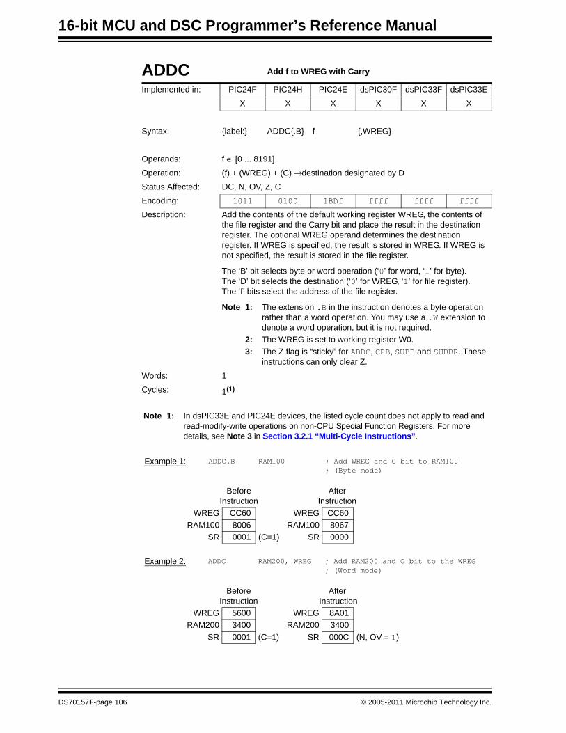
16-bit MCU and DSC Programmer’s Reference Manual
ADDC Add f to WREG with Carry
Implemented in: PIC24F PIC24H PIC24E dsPIC30F dsPIC33F dsPIC33E
X X X X X X
Syntax: {label:} ADDC{.B} f {,WREG}
Operands: f ∈ [0 ... 8191]
Operation: (f) + (WREG) + (C) → destination designated by D
Status Affected: DC, N, OV, Z, C
Encoding: 1011 0100 1BDf ffff ffff ffff
Description: Add the contents of the default working register WREG, the contents of the file register and the Carry bit and place the result in the destination register. The optional WREG operand determines the destination register. If WREG is specified, the result is stored in WREG. If WREG is not specified, the result is stored in the file register.
The ‘B’ bit selects byte or word operation (‘0’ for word, ‘1’ for byte).The ‘D’ bit selects the destination (‘0’ for WREG, ‘1’ for file register).The ‘f’ bits select the address of the file register.
Note 1: The extension .B in the instruction denotes a byte operation rather than a word operation. You may use a .W extension to denote a word operation, but it is not required.
2: The WREG is set to working register W0. 3: The Z flag is “sticky” for ADDC, CPB, SUBB and SUBBR. These
instructions can only clear Z.
Words: 1
Cycles: 1(1)
Note 1: In dsPIC33E and PIC24E devices, the listed cycle count does not apply to read and read-modify-write operations on non-CPU Special Function Registers. For more details, see Note 3 in Section 3.2.1 “Multi-Cycle Instructions”.
Example 1: ADDC.B RAM100 ; Add WREG and C bit to RAM100; (Byte mode)
Before Instruction
AfterInstruction
WREG CC60 WREG CC60 RAM100 8006 RAM100 8067
SR 0001 (C=1) SR 0000
Example 2: ADDC RAM200, WREG ; Add RAM200 and C bit to the WREG; (Word mode)
Before Instruction
AfterInstruction
WREG 5600 WREG 8A01 RAM200 3400 RAM200 3400
SR 0001 (C=1) SR 000C (N, OV = 1)
DS70157F-page 106 © 2005-2011 Microchip Technology Inc.

Section 5. Instruction DescriptionsInstruction
Descriptions
5
ADDC Add Literal to Wn with Carry
Implemented in: PIC24F PIC24H PIC24E dsPIC30F dsPIC33F dsPIC33E
X X X X X X
Syntax: {label:} ADDC{.B} #lit10, Wn
Operands: lit10 ∈ [0 ... 255] for byte operationlit10 ∈ [0 ... 1023] for word operationWn ∈ [W0 ... W15]
Operation: lit10 + (Wn) + (C) → Wn
Status Affected: DC, N, OV, Z, C
Encoding: 1011 0000 1Bkk kkkk kkkk dddd
Description: Add the 10-bit unsigned literal operand, the contents of the working register Wn and the Carry bit, and place the result back into the working register Wn.
The ‘B’ bit selects byte or word operation (‘0’ for word, ‘1’ for byte).The ‘k’ bits specify the literal operand.The ‘d’ bits select the address of the working register.
Note 1: The extension .B in the instruction denotes a byte operation rather than a word operation. You may use a .W extension to denote a word operation, but it is not required.
2: For byte operations, the literal must be specified as an unsigned value [0:255]. See Section 4.6 “Using 10-bit Literal Operands” for information on using 10-bit literal operands in Byte mode.
3: The Z flag is “sticky” for ADDC, CPB, SUBB and SUBBR. These instructions can only clear Z.
Words: 1
Cycles: 1
Example 1: ADDC.B #0xFF, W7 ; Add -1 and C bit to W7 (Byte mode)
Before Instruction
AfterInstruction
W7 12C0 W7 12BFSR 0000 (C = 0) SR 0009 (N,C = 1)
Example 2: ADDC #0xFF, W1 ; Add 255 and C bit to W1 (Word mode)
Before Instruction
AfterInstruction
W1 12C0 W1 13C0SR 0001 (C = 1) SR 0000
© 2005-2011 Microchip Technology Inc. DS70157F-page 107

16-bit MCU and DSC Programmer’s Reference Manual
ADDC Add Wb to Short Literal with Carry
Implemented in: PIC24F PIC24H PIC24E dsPIC30F dsPIC33F dsPIC33E
X X X X X X
Syntax: {label:} ADDC{.B} Wb, #lit5, Wd
[Wd]
[Wd++]
[Wd--]
[++Wd]
[--Wd]
Operands: Wb ∈ [W0 ... W15]lit5 ∈ [0 ... 31]Wd ∈ [W0 ... W15]
Operation: (Wb) + lit5 + (C) → Wd Status Affected: DC, N, OV, Z, C
Encoding: 0100 1www wBqq qddd d11k kkkk
Description: Add the contents of the base register Wb, the 5-bit unsigned short literal operand and the Carry bit, and place the result in the destination register Wd. Register direct addressing must be used for Wb. Register direct or indirect addressing may be used for Wd.
The ‘w’ bits select the address of the base register.The ‘B’ bit selects byte or word operation (‘0’ for word, ‘1’ for byte).The ‘q’ bits select the destination Address mode.The ‘d’ bits select the destination register.The ‘k’ bits provide the literal operand, a five-bit integer number.
Note 1: The extension .B in the instruction denotes a byte operation rather than a word operation. You may use a .W extension to denote a word operation, but it is not required.
2: The Z flag is “sticky” for ADDC, CPB, SUBB and SUBBR. These instructions can only clear Z.
Words: 1Cycles: 1
Example 1: ADDC.B W0, #0x1F, [W7] ; Add W0, 31 and C bit (Byte mode) ; Store the result in [W7]
Before Instruction
AfterInstruction
W0 CC80 W0 CC80W7 12C0 W7 12C0
Data 12C0 B000 Data 12C0 B09FSR 0000 (C = 0) SR 0008 (N = 1)
DS70157F-page 108 © 2005-2011 Microchip Technology Inc.

Section 5. Instruction DescriptionsInstruction
Descriptions
5
Example 2: ADDC W3, #0x6, [--W4] ; Add W3, 6 and C bit (Word mode); Store the result in [--W4]
Before Instruction
AfterInstruction
W3 6006 W3 6006W4 1000 W4 0FFE
Data 0FFE DDEE Data 0FFE 600DData 1000 DDEE Data 1000
SRDDEE
SR 0001 (C = 1) 0000
© 2005-2011 Microchip Technology Inc. DS70157F-page 109

16-bit MCU and DSC Programmer’s Reference Manual
ADDC Add Wb to Ws with Carry
Implemented in: PIC24F PIC24H PIC24E dsPIC30F dsPIC33F dsPIC33E
X X X X X X
Syntax: {label:} ADDC{.B} Wb, Ws, Wd
[Ws], [Wd]
[Ws++], [Wd++]
[Ws--], [Wd--]
[++Ws], [++Wd]
[--Ws], [--Wd]
Operands: Wb ∈ [W0 ... W15]Ws ∈ [W0 ... W15]Wd ∈ [W0 ... W15]
Operation: (Wb) + (Ws) + (C) → Wd
Status Affected: DC, N, OV, Z, C
Encoding: 0100 1www wBqq qddd dppp ssss
Description: Add the contents of the source register Ws, the contents of the base register Wb and the Carry bit, and place the result in the destination register Wd. Register direct addressing must be used for Wb. Either register direct or indirect addressing may be used for Ws and Wd.
The ‘w’ bits select the address of the base register.The ‘B’ bit selects byte or word operation (‘0’ for word, ‘1’ for byte).The ‘q’ bits select the destination Address mode.The ‘d’ bits select the destination register.The ‘p’ bits select the source Address mode.The ‘s’ bits select the source register.
Note 1: The extension .B in the instruction denotes a byte operation rather than a word operation. You may use a .W extension to denote a word operation, but it is not required.
2: The Z flag is “sticky” for ADDC, CPB, SUBB and SUBBR. These instructions can only clear Z.
Words: 1
Cycles: 1(1)
Note 1: In dsPIC33E and PIC24E devices, the listed cycle count does not apply to read and read-modify-write operations on non-CPU Special Function Registers. For more details, see Note 3 in Section 3.2.1 “Multi-Cycle Instructions”.
DS70157F-page 110 © 2005-2011 Microchip Technology Inc.

Section 5. Instruction DescriptionsInstruction
Descriptions
5
Example 1: ADDC.B W0,[W1++],[W2++] ; Add W0, [W1] and C bit (Byte mode); Store the result in [W2]; Post-increment W1, W2
Before Instruction
AfterInstruction
W0 CC20 W0 CC20W1 0800 W1 0801W2 1000 W2 1001
Data 0800 AB25 Data 0800 AB25Data 1000 FFFF Data 1000 FF46
SR 0001 (C = 1) SR 0000
Example 2: ADDC W3,[W2++],[W1++] ; Add W3, [W2] and C bit (Word mode); Store the result in [W1]; Post-increment W1, W2
Before Instruction
AfterInstruction
W1 1000 W1 1002W2 2000 W2 2002W3 0180 W3 0180
Data 1000 8000 Data 1000 2681Data 2000 2500 Data 2000 2500
SR 0001 (C = 1) SR 0000
© 2005-2011 Microchip Technology Inc. DS70157F-page 111
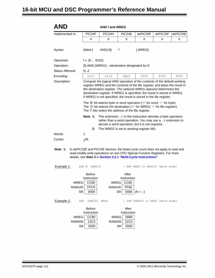
16-bit MCU and DSC Programmer’s Reference Manual
AND AND f and WREG
Implemented in: PIC24F PIC24H PIC24E dsPIC30F dsPIC33F dsPIC33E
X X X X X X
Syntax: {label:} AND{.B} f {,WREG}
Operands: f ∈ [0 ... 8191]
Operation: (f).AND.(WREG) → destination designated by D
Status Affected: N, Z
Encoding: 1011 0110 0BDf ffff ffff ffff
Description: Compute the logical AND operation of the contents of the default working register WREG and the contents of the file register, and place the result in the destination register. The optional WREG operand determines the destination register. If WREG is specified, the result is stored in WREG. If WREG is not specified, the result is stored in the file register.
The ‘B’ bit selects byte or word operation (‘0’ for word, ‘1’ for byte).The ‘D’ bit selects the destination (‘0’ for WREG, ‘1’ for file register).The ‘f’ bits select the address of the file register.
Note 1: The extension .B in the instruction denotes a byte operation rather than a word operation. You may use a .W extension to denote a word operation, but it is not required.
2: The WREG is set to working register W0.
Words: 1
Cycles: 1(1)
Note 1: In dsPIC33E and PIC24E devices, the listed cycle count does not apply to read and read-modify-write operations on non-CPU Special Function Registers. For more details, see Note 3 in Section 3.2.1 “Multi-Cycle Instructions”.
Example 1: AND.B RAM100 ; AND WREG to RAM100 (Byte mode)
Before Instruction
AfterInstruction
WREG CC80 WREG CC80 RAM100 FFC0 RAM100 FF80
SR 0000 SR 0008 (N = 1)
Example 2: AND RAM200, WREG ; AND RAM200 to WREG (Word mode)
Before Instruction
AfterInstruction
WREG CC80 WREG 0080 RAM200 12C0 RAM200 12C0
SR 0000 SR 0000
DS70157F-page 112 © 2005-2011 Microchip Technology Inc.

Section 5. Instruction DescriptionsInstruction
Descriptions
5
AND AND Literal and Wn
Implemented in: PIC24F PIC24H PIC24E dsPIC30F dsPIC33F dsPIC33E
X X X X X X
Syntax: {label:} AND{.B} #lit10, Wn
Operands: lit10 ∈ [0 ... 255] for byte operationlit10 ∈ [0 ... 1023] for word operationWn ∈ [W0 ... W15]
Operation: lit10.AND.(Wn) → Wn
Status Affected: N, Z
Encoding: 1011 0010 0Bkk kkkk kkkk dddd
Description: Compute the logical AND operation of the 10-bit literal operand and the contents of the working register Wn and place the result back into the working register Wn. Register direct addressing must be used for Wn.
The ‘B’ bit selects byte or word operation (‘0’ for word, ‘1’ for byte).The ‘k’ bits specify the literal operand.The ‘d’ bits select the address of the working register.
Note 1: The extension .B in the instruction denotes a byte operation rather than a word operation. You may use a .W extension to denote a word operation, but it is not required.
2: For byte operations, the literal must be specified as an unsigned value [0:255]. See Section 4.6 “Using 10-bit Literal Operands” for information on using 10-bit literal operands in Byte mode.
Words: 1
Cycles: 1
Example 1: AND.B #0x83, W7 ; AND 0x83 to W7 (Byte mode)
Before Instruction
AfterInstruction
W7 12C0 W7 1280SR 0000 SR 0008 (N = 1)
Example 2: AND #0x333, W1 ; AND 0x333 to W1 (Word mode)
Before Instruction
AfterInstruction
W1 12D0 W1 0210SR 0000 SR 0000
© 2005-2011 Microchip Technology Inc. DS70157F-page 113

16-bit MCU and DSC Programmer’s Reference Manual
AND AND Wb and Short Literal
Implemented in: PIC24F PIC24H PIC24E dsPIC30F dsPIC33F dsPIC33EX X X X X X
Syntax: {label:} AND{.B} Wb, #lit5, Wd[Wd][Wd++][Wd--][++Wd][--Wd]
Operands: Wb ∈ [W0 ... W15]lit5 ∈ [0 ... 31]Wd ∈ [W0 ... W15]
Operation: (Wb).AND.lit5 → Wd Status Affected: N, ZEncoding: 0110 0www wBqq qddd d11k kkkk
Description: Compute the logical AND operation of the contents of the base register Wb and the 5-bit literal and place the result in the destination register Wd. Register direct addressing must be used for Wb. Either register direct or indirect addressing may be used for Wd.
The ‘w’ bits select the address of the base register.The ‘B’ bit selects byte or word operation (‘0’ for word, ‘1’ for byte).The ‘q’ bits select the destination Address mode.The ‘d’ bits select the destination register.The ‘k’ bits provide the literal operand, a five-bit integer number.
Note: The extension .B in the instruction denotes a byte operation rather than a word operation. You may use a .W extension to denote a word operation, but it is not required.
Words: 1Cycles: 1
Example 1: AND.B W0,#0x3,[W1++] ; AND W0 and 0x3 (Byte mode); Store to [W1]; Post-increment W1
Before Instruction
AfterInstruction
W0 23A5 W0 23A5W1 2211 W1 2212
Data 2210 9999 Data 2210 0199SR 0000 SR 0000
Example 2: AND W0,#0x1F,W1 ; AND W0 and 0x1F (Word mode); Store to W1
Before Instruction
AfterInstruction
W0 6723 W0 6723W1 7878 W1 0003SR 0000 SR 0000
DS70157F-page 114 © 2005-2011 Microchip Technology Inc.

Section 5. Instruction DescriptionsInstruction
Descriptions
5
AND And Wb and Ws
Implemented in: PIC24F PIC24H PIC24E dsPIC30F dsPIC33F dsPIC33E
X X X X X X
Syntax: {label:} AND{.B} Wb, Ws, Wd
[Ws], [Wd]
[Ws++], [Wd++]
[Ws--], [Wd--]
[++Ws], [++Wd]
[--Ws], [--Wd]
Operands: Wb ∈ [W0 ... W15]Ws ∈ [W0 ... W15]Wd ∈ [W0 ... W15]
Operation: (Wb).AND.(Ws) → Wd Status Affected: N, Z
Encoding: 0110 0www wBqq qddd dppp ssss
Description: Compute the logical AND operation of the contents of the source register Ws and the contents of the base register Wb, and place the result in the destination register Wd. Register direct addressing must be used for Wb. Either register direct or indirect addressing may be used for Ws and Wd.
The ‘w’ bits select the address of the base register.The ‘B’ bit selects byte or word operation (‘0’ for word, ‘1’ for byte).The ‘q’ bits select the destination Address mode.The ‘d’ bits select the destination register.The ‘p’ bits select the source Address mode.The ‘s’ bits select the source register.
Note: The extension .B in the instruction denotes a byte operation rather than a word operation. You may use a .W extension to denote a word operation, but it is not required.
Words: 1Cycles: 1(1)
Note 1: In dsPIC33E and PIC24E devices, the listed cycle count does not apply to read and read-modify-write operations on non-CPU Special Function Registers. For more details, see Note 3 in Section 3.2.1 “Multi-Cycle Instructions”.
© 2005-2011 Microchip Technology Inc. DS70157F-page 115

16-bit MCU and DSC Programmer’s Reference Manual
Example 1: AND.B W0, W1 [W2++] ; AND W0 and W1, and; store to [W2] (Byte mode); Post-increment W2
Before Instruction
AfterInstruction
W0 AA55 W0 AA55W1 2211 W1 2211W2 1001 W2 1002
Data 1000 FFFF Data 1000 11FFSR 0000 SR 0000
Example 2: AND W0, [W1++], W2 ; AND W0 and [W1], and; store to W2 (Word mode); Post-increment W1
Before Instruction
AfterInstruction
W0 AA55 W0 AA55W1 1000 W1 1002W2 55AA W2 2214
Data 1000 2634 Data 1000 2634SR 0000 SR 0000
DS70157F-page 116 © 2005-2011 Microchip Technology Inc.

Section 5. Instruction DescriptionsInstruction
Descriptions
5
ASR Arithmetic Shift Right f
Implemented in: PIC24F PIC24H PIC24E dsPIC30F dsPIC33F dsPIC33E
X X X X X X
Syntax: {label:} ASR{.B} f {,WREG}
Operands: f ∈ [0 ... 8191]
Operation: For byte operation: (f<7>) → Dest<7> (f<7>) → Dest<6> (f<6:1>) → Dest<5:0> (f<0>) → CFor word operation: (f<15>) → Dest<15> (f<15>) → Dest<14> (f<14:1>) → Dest<13:0> (f<0>) → C
Status Affected: N, Z, C
Encoding: 1101 0101 1BDf ffff ffff ffff
Description: Shift the contents of the file register one bit to the right and place the result in the destination register. The Least Significant bit of the file register is shifted into the Carry bit of the STATUS Register. After the shift is performed, the result is sign-extended. The optional WREG operand determines the destination register. If WREG is specified, the result is stored in WREG. If WREG is not specified, the result is stored in the file register.
The ‘B’ bit selects byte or word operation (‘0’ for word, ’1’ for byte).The ‘D’ bit selects the destination (‘0’ for WREG, ‘1’ for file register).The ‘f’ bits select the address of the file register.
Note 1: The extension .B in the instruction denotes a byte operation rather than a word operation. You may use a .W extension to denote a word operation, but it is not required.
2: The WREG is set to working register W0.
Words: 1
Cycles: 1(1)
Note 1: In dsPIC33E and PIC24E devices, the listed cycle count does not apply to read and read-modify-write operations on non-CPU Special Function Registers. For more details, see Note 3 in Section 3.2.1 “Multi-Cycle Instructions”.
C
© 2005-2011 Microchip Technology Inc. DS70157F-page 117

16-bit MCU and DSC Programmer’s Reference Manual
Example 1: ASR.B RAM400, WREG ; ASR RAM400 and store to WREG ; (Byte mode)
Before Instruction
AfterInstruction
WREG 0600 WREG 0611RAM400 0823 RAM400 0823
SR 0000 SR 0001 (C = 1)
Example 2: ASR RAM200 ; ASR RAM200 (Word mode)
Before Instruction
AfterInstruction
RAM200 8009 RAM200 C004SR 0000 SR 0009 (N, C = 1)
DS70157F-page 118 © 2005-2011 Microchip Technology Inc.
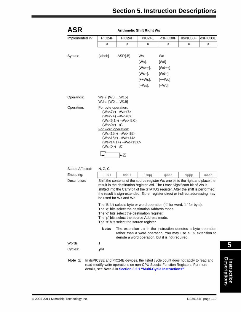
Section 5. Instruction DescriptionsInstruction
Descriptions
5
ASR Arithmetic Shift Right Ws
Implemented in: PIC24F PIC24H PIC24E dsPIC30F dsPIC33F dsPIC33E
X X X X X X
Syntax: {label:} ASR{.B} Ws, Wd
[Ws], [Wd]
[Ws++], [Wd++]
[Ws--], [Wd--]
[++Ws], [++Wd]
[--Ws], [--Wd]
Operands: Ws ∈ [W0 ... W15]Wd ∈ [W0 ... W15]
Operation: For byte operation: (Ws<7>) → Wd<7> (Ws<7>) → Wd<6> (Ws<6:1>) → Wd<5:0> (Ws<0>) → CFor word operation: (Ws<15>) → Wd<15> (Ws<15>) → Wd<14> (Ws<14:1>) → Wd<13:0> (Ws<0>) → C
Status Affected: N, Z, C
Encoding: 1101 0001 1Bqq qddd dppp ssss
Description: Shift the contents of the source register Ws one bit to the right and place the result in the destination register Wd. The Least Significant bit of Ws is shifted into the Carry bit of the STATUS register. After the shift is performed, the result is sign-extended. Either register direct or indirect addressing may be used for Ws and Wd.
The ‘B’ bit selects byte or word operation (‘0’ for word, ‘1’ for byte).The ‘q’ bits select the destination Address mode.The ‘d’ bits select the destination register.The ‘p’ bits select the source Address mode.The ‘s’ bits select the source register.
Note: The extension .B in the instruction denotes a byte operation rather than a word operation. You may use a .W extension to denote a word operation, but it is not required.
Words: 1
Cycles: 1(1)
Note 1: In dsPIC33E and PIC24E devices, the listed cycle count does not apply to read and read-modify-write operations on non-CPU Special Function Registers. For more details, see Note 3 in Section 3.2.1 “Multi-Cycle Instructions”.
C
© 2005-2011 Microchip Technology Inc. DS70157F-page 119
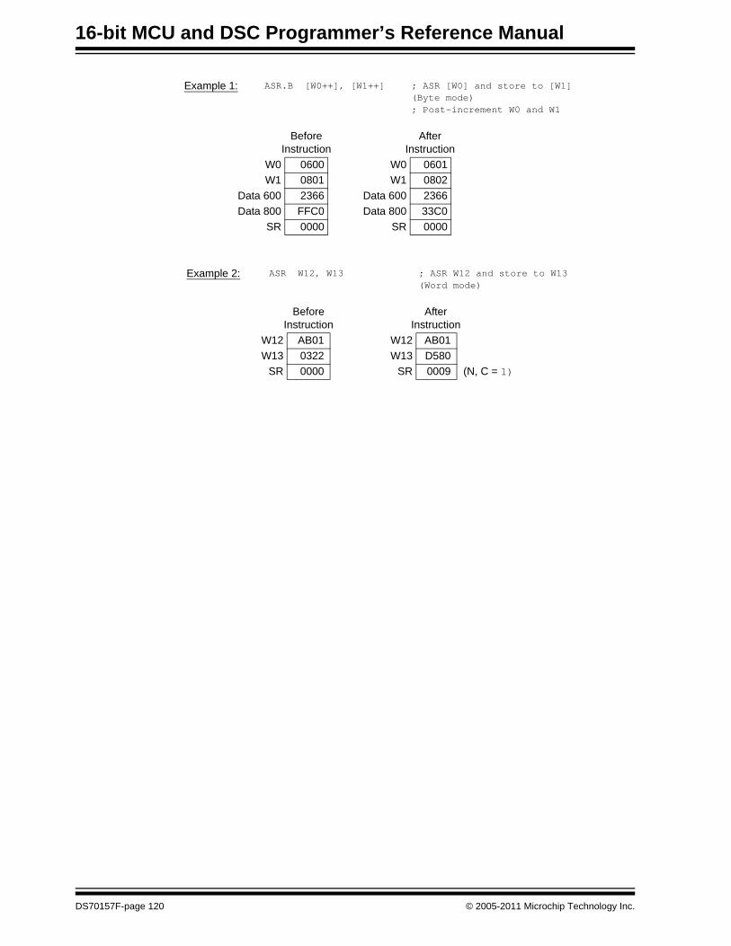
16-bit MCU and DSC Programmer’s Reference Manual
Example 1: ASR.B [W0++], [W1++] ; ASR [W0] and store to [W1] (Byte mode); Post-increment W0 and W1
BeforeInstruction
AfterInstruction
W0 0600 W0 0601W1 0801 W1 0802
Data 600 2366 Data 600 2366 Data 800 FFC0 Data 800 33C0
SR 0000 SR 0000
Example 2: ASR W12, W13 ; ASR W12 and store to W13 (Word mode)
Before Instruction
AfterInstruction
W12 AB01 W12 AB01W13 0322 W13 D580
SR 0000 SR 0009 (N, C = 1)
DS70157F-page 120 © 2005-2011 Microchip Technology Inc.

Section 5. Instruction DescriptionsInstruction
Descriptions
5
ASR Arithmetic Shift Right by Short Literal
Implemented in: PIC24F PIC24H PIC24E dsPIC30F dsPIC33F dsPIC33E
X X X X X X
Syntax: {label:} ASR Wb, #lit4, Wnd
Operands: Wb ∈ [W0 ... W15]lit4 ∈ [0...15]Wnd ∈ [W0 ... W15]
Operation: lit4<3:0> → Shift_ValWb<15> → Wnd<15:15-Shift_Val + 1>Wb<15:Shift_Val> → Wnd<15-Shift_Val:0>
Status Affected: N, Z
Encoding: 1101 1110 1www wddd d100 kkkk
Description: Arithmetic shift right the contents of the source register Wb by the 4-bit unsigned literal, and store the result in the destination register Wnd. After the shift is performed, the result is sign-extended. Direct addressing must be used for Wb and Wnd.
The ‘w’ bits select the address of the base register.The ‘d’ bits select the destination register.The ‘k’ bits provide the literal operand.
Note: This instruction operates in Word mode only.
Words: 1
Cycles: 1
Example 1: ASR W0, #0x4, W1 ; ASR W0 by 4 and store to W1
Before Instruction
AfterInstruction
W0 060F W0 060FW1 1234 W1 0060SR 0000 SR 0000
Example 2: ASR W0, #0x6, W1 ; ASR W0 by 6 and store to W1
Before Instruction
AfterInstruction
W0 80FF W0 80FFW1 0060 W1 FE03SR 0000 SR 0008 (N = 1)
Example 3: ASR W0, #0xF, W1 ; ASR W0 by 15 and store to W1
Before Instruction
AfterInstruction
W0 70FF W0 70FFW1 CC26 W1 0000SR 0000 SR 0002 (Z = 1)
© 2005-2011 Microchip Technology Inc. DS70157F-page 121
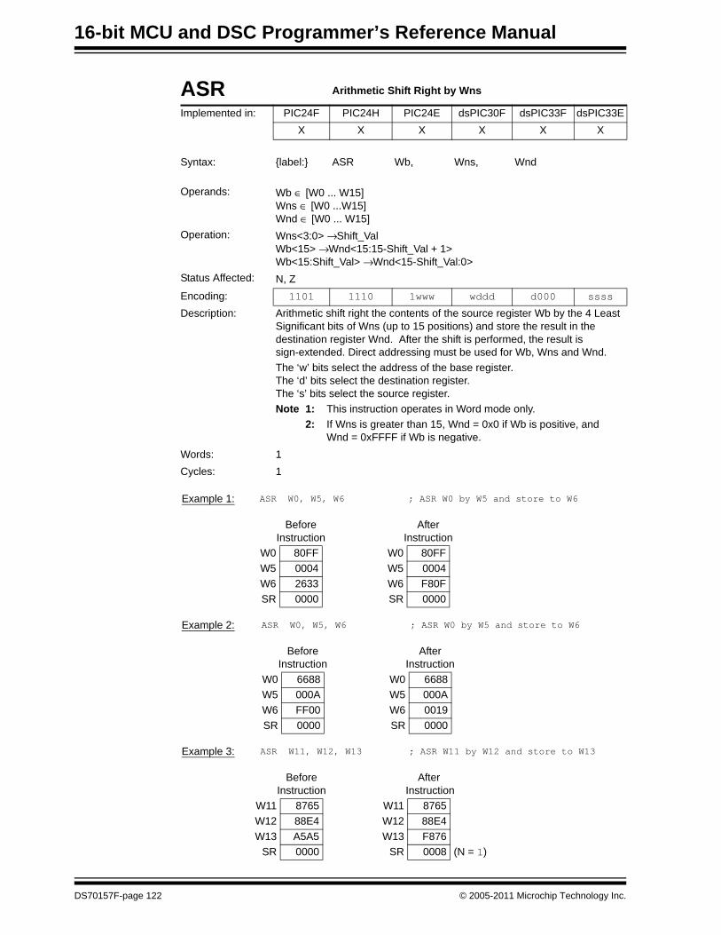
16-bit MCU and DSC Programmer’s Reference Manual
ASR Arithmetic Shift Right by Wns
Implemented in: PIC24F PIC24H PIC24E dsPIC30F dsPIC33F dsPIC33EX X X X X X
Syntax: {label:} ASR Wb, Wns, Wnd
Operands: Wb ∈ [W0 ... W15]Wns ∈ [W0 ...W15]Wnd ∈ [W0 ... W15]
Operation: Wns<3:0> → Shift_ValWb<15> → Wnd<15:15-Shift_Val + 1>Wb<15:Shift_Val> → Wnd<15-Shift_Val:0>
Status Affected: N, ZEncoding: 1101 1110 1www wddd d000 ssss
Description: Arithmetic shift right the contents of the source register Wb by the 4 Least Significant bits of Wns (up to 15 positions) and store the result in the destination register Wnd. After the shift is performed, the result is sign-extended. Direct addressing must be used for Wb, Wns and Wnd.The ‘w’ bits select the address of the base register.The ‘d’ bits select the destination register.The ‘s’ bits select the source register.Note 1: This instruction operates in Word mode only.
2: If Wns is greater than 15, Wnd = 0x0 if Wb is positive, and Wnd = 0xFFFF if Wb is negative.
Words: 1Cycles: 1
Example 1: ASR W0, W5, W6 ; ASR W0 by W5 and store to W6
Before Instruction
AfterInstruction
W0 80FF W0 80FFW5 0004 W5 0004W6 2633 W6 F80FSR 0000 SR 0000
Example 2: ASR W0, W5, W6 ; ASR W0 by W5 and store to W6
Before Instruction
AfterInstruction
W0 6688 W0 6688W5 000A W5 000AW6 FF00 W6 0019SR 0000 SR 0000
Example 3: ASR W11, W12, W13 ; ASR W11 by W12 and store to W13
Before Instruction
AfterInstruction
W11 8765 W11 8765W12 88E4 W12 88E4W13 A5A5 W13 F876
SR 0000 SR 0008 (N = 1)
DS70157F-page 122 © 2005-2011 Microchip Technology Inc.

Section 5. Instruction DescriptionsInstruction
Descriptions
5
BCLR Bit Clear f
Implemented in: PIC24F PIC24H PIC24E dsPIC30F dsPIC33F dsPIC33E
X X X X X X
Syntax: {label:} BCLR{.B} f, #bit4
Operands: f ∈ [0 ... 8191] for byte operationf ∈ [0 ... 8190] (even only) for word operationbit4 ∈ [0 ... 7] for byte operationbit4 ∈ [0 ... 15] for byte operation
Operation: 0 → f<bit4>
Status Affected: None
Encoding: 1010 1001 bbbf ffff ffff fffb
Description: Clear the bit in the file register f specified by ‘bit4’. Bit numbering begins with the Least Significant bit (bit 0) and advances to the Most Significant bit (bit 7 for byte operations, bit 15 for word operations).
The ‘b’ bits select value bit4 of the bit position to be cleared.The ‘f’ bits select the address of the file register.
Note 1: The extension .B in the instruction denotes a byte operation rather than a word operation. You may use a .W extension to denote a word operation, but it is not required.
2: When this instruction operates in Word mode, the file register address must be word-aligned.
3: When this instruction operates in Byte mode, ‘bit4’ must be between 0 and 7.
Words: 1
Cycles: 1(1)
Note 1: In dsPIC33E and PIC24E devices, the listed cycle count does not apply to read and read-modify-write operations on non-CPU Special Function Registers. For more details, see Note 3 in Section 3.2.1 “Multi-Cycle Instructions”.
Example 1: BCLR.B 0x800, #0x7 ; Clear bit 7 in 0x800
Before Instruction
AfterInstruction
Data 0800 66EF Data 0800 666FSR 0000 SR 0000
Example 2: BCLR 0x400, #0x9 ; Clear bit 9 in 0x400
Before Instruction
AfterInstruction
Data 0400 AA55 Data 0400 A855SR 0000 SR 0000
© 2005-2011 Microchip Technology Inc. DS70157F-page 123

16-bit MCU and DSC Programmer’s Reference Manual
BCLR Bit Clear in Ws
Implemented in: PIC24F PIC24H PIC24E dsPIC30F dsPIC33F dsPIC33E
X X X X X X
Syntax: {label:} BCLR{.B} Ws, #bit4
[Ws],
[Ws++],
[Ws--],
[++Ws],
[--Ws],
Operands: Ws ∈ [W0 ... W15]bit4 ∈ [0 ... 7] for byte operationbit4 ∈ [0 ... 15] for word operation
Operation: 0 → Ws<bit4>
Status Affected: None
Encoding: 1010 0001 bbbb 0B00 0ppp ssss
Description: Clear the bit in register Ws specified by ‘bit4’. Bit numbering begins with the Least Significant bit (bit 0) and advances to the Most Significant bit (bit 7 for byte operations, bit 15 for word operations). Register direct or indirect addressing may be used for Ws.
The ‘b’ bits select value bit4 of the bit position to be cleared.The ‘B’ bit selects byte or word operation (‘0’ for word, ‘1’ for byte).The ‘s’ bits select the source/destination register.The ‘p’ bits select the source Address mode.
Note 1: The extension .B in the instruction denotes a byte operation rather than a word operation. You may use a .W extension to denote a word operation, but it is not required.
2: When this instruction operates in Word mode, the source register address must be word-aligned.
3: When this instruction operates in Byte mode, ‘bit4’ must be between 0 and 7.
4: In dsPIC33E and PIC24E devices, this instruction uses the DSRPAG register for indirect address generation in Extended Data Space.
Words: 1
Cycles: 1(1)
Note 1: In dsPIC33E and PIC24E devices, the listed cycle count does not apply to read and read-modify-write operations on non-CPU Special Function Registers. For more details, see Note 3 in Section 3.2.1 “Multi-Cycle Instructions”.
DS70157F-page 124 © 2005-2011 Microchip Technology Inc.

Section 5. Instruction DescriptionsInstruction
Descriptions
5
Example 1: BCLR.B W2, #0x2 ; Clear bit 3 in W2
Before Instruction
AfterInstruction
W2 F234 W2 F230SR 0000 SR 0000
Example 2: BCLR [W0++], #0x0 ; Clear bit 0 in [W0]; Post-increment W0
Before Instruction
AfterInstruction
W0 2300 W0 2302Data 2300 5607 Data 2300 5606
SR 0000 SR 0000
© 2005-2011 Microchip Technology Inc. DS70157F-page 125

16-bit MCU and DSC Programmer’s Reference Manual
BRA Branch Unconditionally
Implemented in: PIC24F PIC24H PIC24E dsPIC30F dsPIC33F dsPIC33EX X X X X X
Syntax: {label:} BRA Expr
Operands: Expr may be a label, absolute address or expression. Expr is resolved by the linker to a Slit16, where Slit16 ∈ [-32768 ... +32767].
Operation: (PC + 2) + 2 * Slit16 → PCNOP → Instruction Register
Status Affected: NoneEncoding: 0011 0111 nnnn nnnn nnnn nnnn
Description: The program will branch unconditionally, relative to the next PC. The offset of the branch is the two’s complement number ‘2 * Slit16’, which supports branches up to 32K instructions forward or backward. The Slit16 value is resolved by the linker from the supplied label, absolute address or expression. After the branch is taken, the new address will be (PC + 2) + 2 * Slit16, since the PC will have incremented to fetch the next instruction.The ‘n’ bits are a signed literal that specifies the number of program words offset from (PC + 2).
Words: 1Cycles: 2 (PIC24F, PIC24H, dsPIC30F, dsPIC33F)
4 (PIC24E, dsPIC33E)
Example 1: 002000 HERE: BRA THERE002002 . . .002004 . . .002006 . . .002008 . . .00200A THERE: . . .00200C . . .
; Branch to THERE
Before Instruction
After Instruction
PC 00 2000 PC 00 200ASR 0000 SR 0000
Example 2: 002000 HERE: BRA THERE+0x2002002 . . .002004 . . .002006 . . .002008 . . .00200A THERE: . . .00200C . . .
; Branch to THERE+0x2
Before Instruction
After Instruction
PC 00 2000 PC 00 200CSR 0000 SR 0000
DS70157F-page 126 © 2005-2011 Microchip Technology Inc.

Section 5. Instruction DescriptionsInstruction
Descriptions
5
Example 3: 002000 HERE: BRA 0x1366002002 . . .002004 . . .
; Branch to 0x1366
Before Instruction
After Instruction
PC 00 2000 PC 00 1366SR 0000 SR 0000
© 2005-2011 Microchip Technology Inc. DS70157F-page 127

16-bit MCU and DSC Programmer’s Reference Manual
BRA Computed Branch
Implemented in: PIC24F PIC24H PIC24E dsPIC30F dsPIC33F dsPIC33E
X X X X
Syntax: {label:} BRA Wn
Operands: Wn ∈ [W0 ... W15]
Operation: (PC + 2) + (2 * Wn) → PCNOP → Instruction Register
Status Affected: None
Encoding: 0000 0001 0110 0000 0000 ssss
Description: The program branches unconditionally, relative to the next PC. The offset of the branch is the sign-extended 17-bit value (2 * Wn), which supports branches up to 32K instructions forward or backward. After this instruction executes, the new PC will be (PC + 2) + 2 * Wn, since the PC will have incremented to fetch the next instruction.
The ‘s’ bits select the source register.
Words: 1
Cycles: 2
Example 1: 002000 HERE: BRA W7002002 . . . ... . . . ... . . .002108 . . .00210A TABLE7: . . .00210C . . .
; Branch forward (2+2*W7)
Before Instruction
After Instruction
PC 00 2000 PC 00 210AW7 0084 W7 0084 SR 0000 SR 0000
DS70157F-page 128 © 2005-2011 Microchip Technology Inc.

Section 5. Instruction DescriptionsInstruction
Descriptions
5
BRA Computed Branch
Implemented in: PIC24F PIC24H PIC24E dsPIC30F dsPIC33F dsPIC33E
X X
Syntax: {label:} BRA Wn
Operands: Wn ∈ [W0 ... W15]
Operation: (PC + 2) + (2 * Wn) → PCNOP → Instruction Register
Status Affected: None
Encoding: 0000 0001 0000 0110 0000 ssss
Description: The program branches unconditionally, relative to the next PC. The offset of the branch is the sign-extended 17-bit value (2 * Wn), which supports branches up to 32K instructions forward or backward. After this instruction executes, the new PC will be (PC + 2) + 2 * Wn, since the PC will have incremented to fetch the next instruction.
The ‘s’ bits select the source register.
Words: 1
Cycles: 4
Example 1: 002000 HERE: BRA W7002002 . . . ... . . . ... . . .002108 . . .00210A TABLE7: . . .00210C . . .
; Branch forward (2+2*W7)
Before Instruction
After Instruction
PC 00 2000 PC 00 210AW7 0084 W7 0084 SR 0000 SR 0000
© 2005-2011 Microchip Technology Inc. DS70157F-page 129

16-bit MCU and DSC Programmer’s Reference Manual
BRA C Branch if Carry
Implemented in: PIC24F PIC24H PIC24E dsPIC30F dsPIC33F dsPIC33E
X X X X X X
Syntax: {label:} BRA C, Expr
Operands: Expr may be a label, absolute address or expression. Expr is resolved by the linker to a Slit16, where Slit16 ∈ [-32768 ... +32767].
Operation: Condition = CIf (Condition) (PC + 2) + 2 * Slit16 → PC NOP → Instruction Register
Status Affected: None
Encoding: 0011 0001 nnnn nnnn nnnn nnnn
Description: If the Carry flag bit is ‘1’, then the program will branch relative to the next PC. The offset of the branch is the two’s complement number ‘2 * Slit16’, which supports branches up to 32K instructions forward or backward. The Slit16 value is resolved by the linker from the supplied label, absolute address or expression.
If the branch is taken, the new address will be (PC + 2) + 2 * Slit16, since the PC will have incremented to fetch the next instruction. The instruction then becomes a two-cycle instruction, with a NOP executed in the second cycle.
The ‘n’ bits are a 16-bit signed literal that specify the offset from (PC + 2) in instruction words.
Words: 1
Cycles: 1 (2 if branch taken) – PIC24F, PIC24H, dsPIC30F, dsPIC33F
1 (4 if branch taken) – PIC24E, dsPIC33E
Example 1: 002000 HERE: BRA C, CARRY002002 NO_C: . . .002004 . . .002006 GOTO THERE002008 CARRY: . . .00200A . . .00200C THERE: . . .00200E . . .
; If C is set, branch to CARRY; Otherwise... continue
Before Instruction
After Instruction
PC 00 2000 PC 00 2008SR 0001 (C = 1) SR 0001 (C = 1)
DS70157F-page 130 © 2005-2011 Microchip Technology Inc.

Section 5. Instruction DescriptionsInstruction
Descriptions
5
Example 2: 002000 HERE: BRA C, CARRY002002 NO_C: ...002004 ...002006 GOTO THERE002008 CARRY: ...00200A ...00200C THERE: ...00200E ...
; If C is set, branch to CARRY; Otherwise... continue
BeforeInstruction
After Instruction
PC 00 2000 PC 00 2002SR 0000 SR 0000
Example 3: 006230 HERE: BRA C, CARRY006232 NO_C: ...006234 ...006236 GOTO THERE006238 CARRY: ...00623A ...00623C THERE: ...00623E ...
; If C is set, branch to CARRY; Otherwise... continue
Before Instruction
After Instruction
PC 00 6230 PC 00 6238SR 0001 (C = 1) SR 0001 (C = 1)
Example 4: 006230 START: ...006232 ...006234 CARRY: ...006236 ...006238 ...00623A ...00623C HERE: BRA C, CARRY00623E ...
; If C is set, branch to CARRY; Otherwise... continue
Before Instruction
After Instruction
PC 00 623C PC 00 6234SR 0001 (C = 1) SR 0001 (C = 1)
© 2005-2011 Microchip Technology Inc. DS70157F-page 131

16-bit MCU and DSC Programmer’s Reference Manual
BRA GE Branch if Signed Greater Than or Equal
Implemented in: PIC24F PIC24H PIC24E dsPIC30F dsPIC33F dsPIC33EX X X X X X
Syntax: {label:} BRA GE, Expr
Operands: Expr may be a label, absolute address or expression. Expr is resolved by the linker to a Slit16, where Slit16 ∈ [-32768 ... +32767].
Operation: Condition = (N&&OV)||(!N&&!OV)If (Condition) (PC + 2) + 2 * Slit16 → PC NOP → Instruction Register
Status Affected: NoneEncoding: 0011 1101 nnnn nnnn nnnn nnnn
Description: If the logical expression (N&&OV)||(!N&&!OV) is true, then the program will branch relative to the next PC. The offset of the branch is the two’s complement number ‘2 * Slit16’, which supports branches up to 32K instructions forward or backward. The Slit16 value is resolved by the linker from the supplied label, absolute address or expression.
If the branch is taken, the new address will be (PC + 2) + 2 * Slit16, since the PC will have incremented to fetch the next instruction. The instruction then becomes a two-cycle instruction, with a NOP executed in the second cycle.
The ‘n’ bits are a 16-bit signed literal that specify the offset from (PC + 2) in instruction words.
Note: The assembler will convert the specified label into the offset to be used.
Words: 1Cycles: 1 (2 if branch taken) – PIC24F, PIC24H, dsPIC30F, dsPIC33F
1 (4 if branch taken) – PIC24E, dsPIC33E
Example 1: 007600 LOOP: . . .007602 . . .007604 . . .007606 . . .007608 HERE: BRA GE, LOOP00760A NO_GE: . . .
; If GE, branch to LOOP; Otherwise... continue
Before Instruction
After Instruction
PC 00 7608 PC 00 7600SR 0000 SR 0000
DS70157F-page 132 © 2005-2011 Microchip Technology Inc.
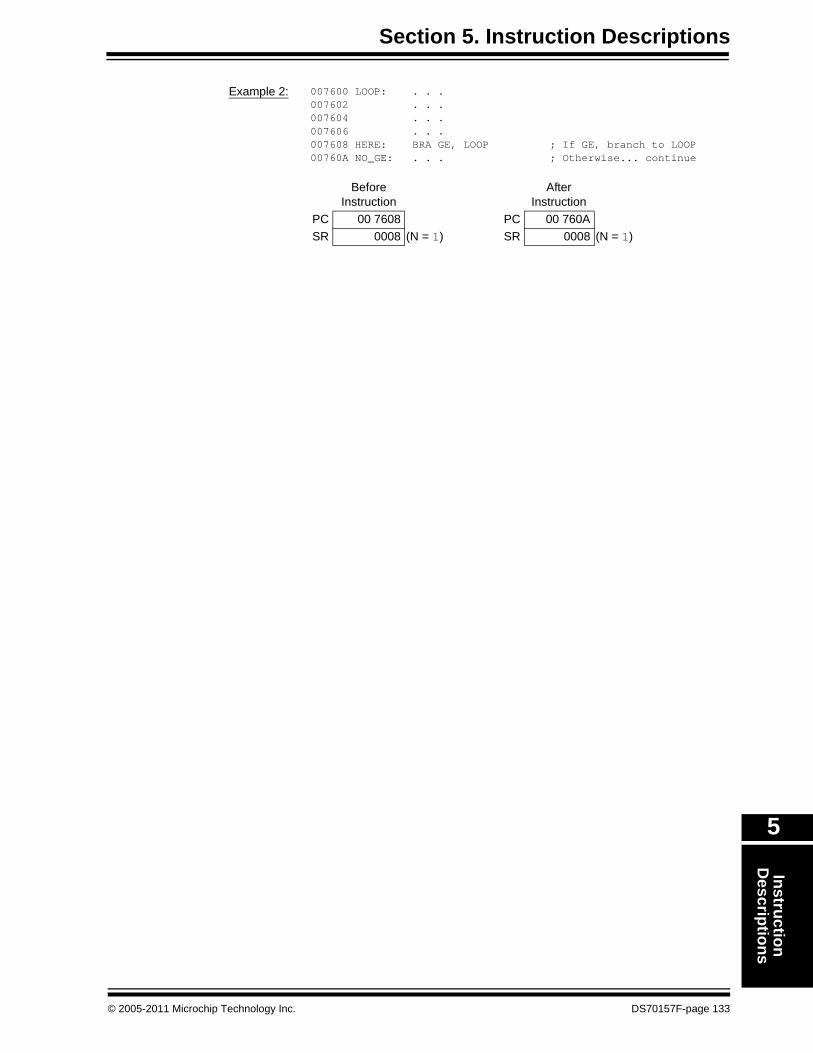
Section 5. Instruction DescriptionsInstruction
Descriptions
5
Example 2: 007600 LOOP: . . .007602 . . .007604 . . .007606 . . .007608 HERE: BRA GE, LOOP00760A NO_GE: . . .
; If GE, branch to LOOP; Otherwise... continue
Before Instruction
After Instruction
PC 00 7608 PC 00 760ASR 0008 (N = 1) SR 0008 (N = 1)
© 2005-2011 Microchip Technology Inc. DS70157F-page 133

16-bit MCU and DSC Programmer’s Reference Manual
BRA GEU Branch if Unsigned Greater Than or Equal
Implemented in: PIC24F PIC24H PIC24E dsPIC30F dsPIC33F dsPIC33E
X X X X X X
Syntax: {label:} BRA GEU, Expr
Operands: Expr may be a label, absolute address or expression. Expr is resolved by the linker to a Slit16 offset that supports an offset range of [-32768 ... +32767] program words.
Operation: Condition = CIf (Condition) (PC + 2) + 2 * Slit16 → PC NOP → Instruction Register
Status Affected: None
Encoding: 0011 0001 nnnn nnnn nnnn nnnn
Description: If the Carry flag is ‘1’, then the program will branch relative to the next PC. The offset of the branch is the two’s complement number ‘2 * Slit16’, which supports branches up to 32K instructions forward or backward. The Slit16 value is resolved by the linker from the supplied label, absolute address or expression.
If the branch is taken, the new address will be (PC + 2) + 2 * Slit16, since the PC will have incremented to fetch the next instruction. The instruction then becomes a two-cycle instruction, with a NOP executed in the second cycle.
The ‘n’ bits are a 16-bit signed literal that specify the offset from (PC + 2) in instruction words.
Note: This instruction is identical to the BRA C, Expr (Branch if Carry) instruction and has the same encoding. It will reverse assemble as BRA C, Slit16.
Words: 1
Cycles: 1 (2 if branch taken) – PIC24F, PIC24H, dsPIC30F, dsPIC33F
1 (4 if branch taken) – PIC24E, dsPIC33E
Example 1: 002000 HERE: BRA GEU, BYPASS002002 NO_GEU: . . .002004 . . .002006 . . .002008 . . .00200A GOTO THERE00200C BYPASS: . . .00200E . . .
; If C is set, branch; to BYPASS; Otherwise... continue
Before Instruction
After Instruction
PC 00 2000 PC 00 200CSR 0001 (C = 1) SR 0001 (C = 1)
DS70157F-page 134 © 2005-2011 Microchip Technology Inc.

Section 5. Instruction DescriptionsInstruction
Descriptions
5
BRA GT Branch if Signed Greater Than
Implemented in: PIC24F PIC24H PIC24E dsPIC30F dsPIC33F dsPIC33E
X X X X X X
Syntax: {label:} BRA GT, Expr
Operands: Expr may be a label, absolute address or expression. Expr is resolved by the linker to a Slit16, where Slit16 ∈ [-32768 ... +32767].
Operation: Condition = (!Z&&N&&OV)||(!Z&&!N&&!OV)If (Condition) (PC + 2) + 2 * Slit16 → PC NOP → Instruction Register
Status Affected: None
Encoding: 0011 1100 nnnn nnnn nnnn nnnn
Description: If the logical expression (!Z&&N&&OV)||(!Z&&!N&&!OV) is true, then the program will branch relative to the next PC. The offset of the branch is the two’s complement number ‘2 * Slit16’, which supports branches up to 32K instructions forward or backward. The Slit16 value is resolved by the linker from the supplied label, absolute address or expression.
If the branch is taken, the new address will be (PC + 2) + 2 * Slit16, since the PC will have incremented to fetch the next instruction. The instruction then becomes a two-cycle instruction, with a NOP executed in the second cycle.
The ‘n’ bits are a 16-bit signed literal that specify the offset from (PC + 2) in instruction words.
Words: 1
Cycles: 1 (2 if branch taken) – PIC24F, PIC24H, dsPIC30F, dsPIC33F
1 (4 if branch taken) – PIC24E, dsPIC33E
Example 1: 002000 HERE: BRA GT, BYPASS002002 NO_GT: . . .002004 . . .002006 . . .002008 . . .00200A GOTO THERE00200C BYPASS: . . .00200E . . .
; If GT, branch to BYPASS; Otherwise... continue
Before Instruction
After Instruction
PC 00 2000 PC 00 200CSR 0001 (C = 1) SR 0001 (C = 1)
© 2005-2011 Microchip Technology Inc. DS70157F-page 135

16-bit MCU and DSC Programmer’s Reference Manual
BRA GTU Branch if Unsigned Greater Than
Implemented in: PIC24F PIC24H PIC24E dsPIC30F dsPIC33F dsPIC33E
X X X X X X
Syntax: {label:} BRA GTU, Expr
Operands: Expr may be a label, absolute address or expression. Expr is resolved by the linker to a Slit16, where Slit16 ∈ [-32768 ... +32767].
Operation: Condition = (C&&!Z)If (Condition) (PC + 2) + 2 * Slit16 → PC NOP → Instruction Register
Status Affected: None
Encoding: 0011 1110 nnnn nnnn nnnn nnnn
Description: If the logical expression (C&&!Z) is true, then the program will branch relative to the next PC. The offset of the branch is the two’s complement number ‘2 * Slit16’, which supports branches up to 32K instructions forward or backward. The Slit16 value is resolved by the linker from the supplied label, absolute address or expression.
If the branch is taken, the new address will be (PC + 2) + 2 * Slit16, since the PC will have incremented to fetch the next instruction. The instruction then becomes a two-cycle instruction, with a NOP executed in the second cycle.
The ‘n’ bits are a signed literal that specifies the number of instructions offset from (PC + 2).
Words: 1
Cycles: 1 (2 if branch taken) – PIC24F, PIC24H, dsPIC30F, dsPIC33F
1 (4 if branch taken) – PIC24E, dsPIC33E
Example 1: 002000 HERE: BRA GTU, BYPASS002002 NO_GTU: . . .002004 . . .002006 . . .002008 . . .00200A GOTO THERE00200C BYPASS: . . .00200E . . .
; If GTU, branch to BYPASS; Otherwise... continue
Before Instruction
After Instruction
PC 00 2000 PC 00 200CSR 0001 (C = 1) SR 0001 (C = 1)
DS70157F-page 136 © 2005-2011 Microchip Technology Inc.

Section 5. Instruction DescriptionsInstruction
Descriptions
5
BRA LE Branch if Signed Less Than or Equal
Implemented in: PIC24F PIC24H PIC24E dsPIC30F dsPIC33F dsPIC33E
X X X X X X
Syntax: {label:} BRA LE, Expr
Operands: Expr may be a label, absolute address or expression. Expr is resolved by the linker to a Slit16, where Slit16 ∈ [-32768 ... +32767].
Operation: Condition = Z||(N&&!OV)||(!N&&OV)If (Condition) (PC + 2) + 2 * Slit16 → PC NOP → Instruction Register
Status Affected: None
Encoding: 0011 0100 nnnn nnnn nnnn nnnn
Description: If the logical expression (Z||(N&&!OV)||(!N&&OV)) is true, then the program will branch relative to the next PC. The offset of the branch is the two’s complement number ‘2 * Slit16’, which supports branches up to 32K instructions forward or backward. The Slit16 value is resolved by the linker from the supplied label, absolute address or expression.
If the branch is taken, the new address will be (PC + 2) + 2 * Slit16, since the PC will have incremented to fetch the next instruction. The instruction then becomes a two-cycle instruction, with a NOP executed in the second cycle.
The ‘n’ bits are a signed literal that specifies the number of instructions offset from (PC + 2).
Words: 1
Cycles: 1 (2 if branch taken) – PIC24F, PIC24H, dsPIC30F, dsPIC33F
1 (4 if branch taken) – PIC24E, dsPIC33E
Example 1: 002000 HERE: BRA LE, BYPASS002002 NO_LE: . . .002004 . . .002006 . . .002008 . . .00200A GOTO THERE00200C BYPASS: . . .00200E . . .
; If LE, branch to BYPASS; Otherwise... continue
Before Instruction
After Instruction
PC 00 2000 PC 00 2002SR 0001 (C = 1) SR 0001 (C = 1)
© 2005-2011 Microchip Technology Inc. DS70157F-page 137

16-bit MCU and DSC Programmer’s Reference Manual
BRA LEU Branch if Unsigned Less Than or Equal
Implemented in: PIC24F PIC24H PIC24E dsPIC30F dsPIC33F dsPIC33E
X X X X X X
Syntax: {label:} BRA LEU, Expr
Operands: Expr may be a label, absolute address or expression. Expr is resolved by the linker to a Slit16, where Slit16 ∈ [-32768 ... +32767].
Operation: Condition = !C||ZIf (Condition) (PC + 2) + 2 * Slit16 → PC NOP → Instruction Register
Status Affected: None
Encoding: 0011 0110 nnnn nnnn nnnn nnnn
Description: If the logical expression (!C||Z) is true, then the program will branch relative to the next PC. The offset of the branch is the two’s complement number ‘2 * Slit16’, which supports branches up to 32K instructions forward or backward. The Slit16 value is resolved by the linker from the supplied label, absolute address or expression.
If the branch is taken, the new address will be (PC + 2) + 2 * Slit16, since the PC will have incremented to fetch the next instruction. The instruction then becomes a two-cycle instruction, with a NOP executed in the second cycle.
The ‘n’ bits are a signed literal that specifies the number of instructions offset from (PC + 2).
Words: 1
Cycles: 1 (2 if branch taken) – PIC24F, PIC24H, dsPIC30F, dsPIC33F
1 (4 if branch taken) – PIC24E, dsPIC33E
Example 1: 002000 HERE: BRA LEU, BYPASS002002 NO_LEU: . . .002004 . . .002006 . . .002008 . . .00200A GOTO THERE00200C BYPASS: . . .00200E . . .
; If LEU, branch to BYPASS; Otherwise... continue
Before Instruction
After Instruction
PC 00 2000 PC 00 200CSR 0001 (C = 1) SR 0001 (C = 1)
DS70157F-page 138 © 2005-2011 Microchip Technology Inc.

Section 5. Instruction DescriptionsInstruction
Descriptions
5
BRA LT Branch if Signed Less Than
Implemented in: PIC24F PIC24H PIC24E dsPIC30F dsPIC33F dsPIC33E
X X X X X X
Syntax: {label:} BRA LT, Expr
Operands: Expr may be a label, absolute address or expression. Expr is resolved by the linker to a Slit16, where Slit16 ∈ [-32768 ... +32767].
Operation: Condition = (N&&!OV)||(!N&&OV)If (Condition) (PC + 2) + 2 * Slit16 → PC NOP → Instruction Register
Status Affected: None
Encoding: 0011 0101 nnnn nnnn nnnn nnnn
Description: If the logical expression ( (N&&!OV)||(!N&&OV) ) is true, then the program will branch relative to the next PC. The offset of the branch is the two’s complement number ‘2 * Slit16’, which supports branches up to 32K instructions forward or backward. The Slit16 value is resolved by the linker from the supplied label, absolute address or expression.
If the branch is taken, the new address will be (PC + 2) + 2 * Slit16, since the PC will have incremented to fetch the next instruction. The instruction then becomes a two-cycle instruction, with a NOP executed in the second cycle.
The ‘n’ bits are a signed literal that specifies the number of instructions offset from (PC + 2).
Words: 1
Cycles: 1 (2 if branch taken) – PIC24F, PIC24H, dsPIC30F, dsPIC33F
1 (4 if branch taken) – PIC24E, dsPIC33E
Example 1: 002000 HERE: BRA LT, BYPASS002002 NO_LT: . . .002004 . . .002006 . . .002008 . . .00200A GOTO THERE00200C BYPASS: . . .00200E . . .
; If LT, branch to BYPASS; Otherwise... continue
Before Instruction
After Instruction
PC 00 2000 PC 00 2002SR 0001 (C = 1) SR 0001 (C = 1)
© 2005-2011 Microchip Technology Inc. DS70157F-page 139

16-bit MCU and DSC Programmer’s Reference Manual
BRA LTU Branch if Unsigned Less Than
Implemented in: PIC24F PIC24H PIC24E dsPIC30F dsPIC33F dsPIC33E
X X X X X X
Syntax: {label:} BRA LTU, Expr
Operands: Expr may be a label, absolute address or expression. Expr is resolved by the linker to a Slit16, where Slit16 ∈ [-32768 ... +32767].
Operation: Condition = !CIf (Condition) (PC + 2) + 2 * Slit16 → PC NOP → Instruction Register
Status Affected: None
Encoding: 0011 1001 nnnn nnnn nnnn nnnn
Description: If the Carry flag is ‘0’, then the program will branch relative to the next PC. The offset of the branch is the two’s complement number ‘2 * Slit16’, which supports branches up to 32K instructions forward or backward. The Slit16 value is resolved by the linker from the supplied label, absolute address or expression.
If the branch is taken, the new address will be (PC + 2) + 2 * Slit16, since the PC will have incremented to fetch the next instruction. The instruction then becomes a two-cycle instruction, with a NOP executed in the second cycle.
The ‘n’ bits are a signed literal that specifies the number of instructions offset from (PC + 2).
Note : This instruction is identical to the BRA NC, Expr (Branch if Not Carry) instruction and has the same encoding. It will reverse assemble as BRA NC, Slit16.
Words: 1
Cycles: 1 (2 if branch taken) – PIC24F, PIC24H, dsPIC30F, dsPIC33F
1 (4 if branch taken) – PIC24E, dsPIC33E
Example 1: 002000 HERE: BRA LTU, BYPASS002002 NO_LTU: . . .002004 . . .002006 . . .002008 . . .00200A GOTO THERE00200C BYPASS: . . .00200E . . .
; If LTU, branch to BYPASS; Otherwise... continue
Before Instruction
After Instruction
PC 00 2000 PC 00 2002SR 0001 (C = 1) SR 0001 (C = 1)
DS70157F-page 140 © 2005-2011 Microchip Technology Inc.

Section 5. Instruction DescriptionsInstruction
Descriptions
5
BRA N Branch if Negative
Implemented in: PIC24F PIC24H PIC24E dsPIC30F dsPIC33F dsPIC33E
X X X X X X
Syntax: {label:} BRA N, Expr
Operands: Expr may be a label, absolute address or expression. Expr is resolved by the linker to a Slit16, where Slit16 ∈ [-32768 ... +32767].
Operation: Condition = NIf (Condition) (PC + 2) + 2 * Slit16 → PC NOP → Instruction Register.
Status Affected: None
Encoding: 0011 0011 nnnn nnnn nnnn nnnn
Description: If the Negative flag is ‘1’, then the program will branch relative to the next PC. The offset of the branch is the two’s complement number ‘2 * Slit16’, which supports branches up to 32K instructions forward or backward. The Slit16 value is resolved by the linker from the supplied label, absolute address or expression.
If the branch is taken, the new address will be (PC + 2) + 2 * Slit16, since the PC will have incremented to fetch the next instruction. The instruction then becomes a two-cycle instruction, with a NOP executed in the second cycle.
The ‘n’ bits are a signed literal that specifies the number of instructions offset from (PC + 2).
Words: 1
Cycles: 1 (2 if branch taken) – PIC24F, PIC24H, dsPIC30F, dsPIC33F
1 (4 if branch taken) – PIC24E, dsPIC33E
Example 1: 002000 HERE: BRA N, BYPASS002002 NO_N: . . .002004 . . .002006 . . .002008 . . .00200A GOTO THERE00200C BYPASS: . . .00200E . . .
; If N, branch to BYPASS; Otherwise... continue
Before Instruction
After Instruction
PC 00 2000 PC 00 200CSR 0008 (N = 1) SR 0008 (N = 1)
© 2005-2011 Microchip Technology Inc. DS70157F-page 141
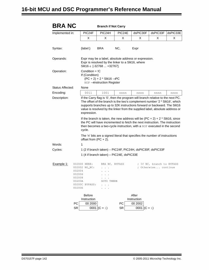
16-bit MCU and DSC Programmer’s Reference Manual
BRA NC Branch if Not Carry
Implemented in: PIC24F PIC24H PIC24E dsPIC30F dsPIC33F dsPIC33E
X X X X X X
Syntax: {label:} BRA NC, Expr
Operands: Expr may be a label, absolute address or expression. Expr is resolved by the linker to a Slit16, where Slit16 ∈ [-32768 ... +32767].
Operation: Condition = !CIf (Condition) (PC + 2) + 2 * Slit16 → PC NOP → Instruction Register
Status Affected: None
Encoding: 0011 1001 nnnn nnnn nnnn nnnn
Description: If the Carry flag is ‘0’, then the program will branch relative to the next PC. The offset of the branch is the two’s complement number ‘2 * Slit16’, which supports branches up to 32K instructions forward or backward. The Slit16 value is resolved by the linker from the supplied label, absolute address or expression.
If the branch is taken, the new address will be (PC + 2) + 2 * Slit16, since the PC will have incremented to fetch the next instruction. The instruction then becomes a two-cycle instruction, with a NOP executed in the second cycle.
The ‘n’ bits are a signed literal that specifies the number of instructions offset from (PC + 2).
Words: 1
Cycles: 1 (2 if branch taken) – PIC24F, PIC24H, dsPIC30F, dsPIC33F
1 (4 if branch taken) – PIC24E, dsPIC33E
Example 1: 002000 HERE: BRA NC, BYPASS002002 NO_NC: . . .002004 . . .002006 . . .002008 . . .00200A GOTO THERE00200C BYPASS: . . .00200E . . .
; If NC, branch to BYPASS; Otherwise... continue
Before Instruction
After Instruction
PC 00 2000 PC 00 2002SR 0001 (C = 1) SR 0001 (C = 1)
DS70157F-page 142 © 2005-2011 Microchip Technology Inc.

Section 5. Instruction DescriptionsInstruction
Descriptions
5
BRA NN Branch if Not Negative
Implemented in: PIC24F PIC24H PIC24E dsPIC30F dsPIC33F dsPIC33E
X X X X X X
Syntax: {label:} BRA NN, Expr
Operands: Expr may be a label, absolute address or expression. Expr is resolved by the linker to a Slit16, where Slit16 ∈ [-32768 ... +32767].
Operation: Condition = !NIf (Condition) (PC + 2) + 2 * Slit16 → PC NOP → Instruction Register
Status Affected: None
Encoding: 0011 1011 nnnn nnnn nnnn nnnn
Description: If the Negative flag is ‘0’, then the program will branch relative to the next PC. The offset of the branch is the two’s complement number ‘2 * Slit16’, which supports branches up to 32K instructions forward or backward. The Slit16 value is resolved by the linker from the supplied label, absolute address or expression.
If the branch is taken, the new address will be (PC + 2) + 2 * Slit16, since the PC will have incremented to fetch the next instruction. The instruction then becomes a two-cycle instruction, with a NOP executed in the second cycle.
The ‘n’ bits are a signed literal that specifies the number of instructions offset from (PC + 2).
Words: 1
Cycles: 1 (2 if branch taken) – PIC24F, PIC24H, dsPIC30F, dsPIC33F
1 (4 if branch taken) – PIC24E, dsPIC33E
Example 1: 002000 HERE: BRA NN, BYPASS002002 NO_NN: . . .002004 . . .002006 . . .002008 . . .00200A GOTO THERE00200C BYPASS: . . .00200E . . .
; If NN, branch to BYPASS; Otherwise... continue
Before Instruction
After Instruction
PC 00 2000 PC 00 200CSR 0000 SR 0000
© 2005-2011 Microchip Technology Inc. DS70157F-page 143

16-bit MCU and DSC Programmer’s Reference Manual
BRA NOV Branch if Not Overflow
Implemented in: PIC24F PIC24H PIC24E dsPIC30F dsPIC33F dsPIC33E
X X X X X X
Syntax: {label:} BRA NOV, Expr
Operands: Expr may be a label, absolute address or expression. Expr is resolved by the linker to a Slit16, where Slit16 ∈ [-32768 ... +32767].
Operation: Condition = !OVIf (Condition) (PC + 2) + 2 * Slit16 → PC NOP → Instruction Register
Status Affected: None
Encoding: 0011 1000 nnnn nnnn nnnn nnnn
Description: If the Overflow flag is ‘0’, then the program will branch relative to the next PC. The offset of the branch is the two’s complement number ‘2 * Slit16’, which supports branches up to 32K instructions forward or backward. The Slit16 value is resolved by the linker from the supplied label, absolute address or expression.
If the branch is taken, the new address will be (PC + 2) + 2 * Slit16, since the PC will have incremented to fetch the next instruction. The instruction then becomes a two-cycle instruction, with a NOP executed in the second cycle.
The ‘n’ bits are a signed literal that specifies the number of instructions offset from (PC + 2).
Words: 1
Cycles: 1 (2 if branch taken) – PIC24F, PIC24H, dsPIC30F, dsPIC33F
1 (4 if branch taken) – PIC24E, dsPIC33E
Example 1: 002000 HERE: BRA NOV, BYPASS002002 NO_NOV: . . .002004 . . .002006 . . .002008 . . .00200A GOTO THERE00200C BYPASS: . . .00200E . . .
; If NOV, branch to BYPASS; Otherwise... continue
Before Instruction
After Instruction
PC 00 2000 PC 00 200CSR 0008 (N = 1) SR 0008 (N = 1)
DS70157F-page 144 © 2005-2011 Microchip Technology Inc.

Section 5. Instruction DescriptionsInstruction
Descriptions
5
BRA NZ Branch if Not Zero
Implemented in: PIC24F PIC24H PIC24E dsPIC30F dsPIC33F dsPIC33E
X X X X X X
Syntax: {label:} BRA NZ, Expr
Operands: Expr may be a label, absolute address or expression. Expr is resolved by the linker to a Slit16, where Slit16 ∈ [-32768 ... +32767].
Operation: Condition = !ZIf (Condition) (PC + 2) + 2 * Slit16 → PC NOP → Instruction Register
Status Affected: None
Encoding: 0011 1010 nnnn nnnn nnnn nnnn
Description: If the Z flag is ‘0’, then the program will branch relative to the next PC. The offset of the branch is the two’s complement number ‘2 * Slit16’, which supports branches up to 32K instructions forward or backward. The Slit16 value is resolved by the linker from the supplied label, absolute address or expression.
If the branch is taken, the new address will be (PC + 2) + 2 * Slit16, since the PC will have incremented to fetch the next instruction. The instruction then becomes a two-cycle instruction, with a NOP executed in the second cycle.
The ‘n’ bits are a signed literal that specifies the number of instructions offset from (PC + 2).
Words: 1
Cycles: 1 (2 if branch taken) – PIC24F, PIC24H, dsPIC30F, dsPIC33F
1 (4 if branch taken) – PIC24E, dsPIC33E
Example 1: 002000 HERE: BRA NZ, BYPASS002002 NO_NZ: . . .002004 . . .002006 . . .002008 . . .00200A GOTO THERE00200C BYPASS: . . .00200E . . .
; If NZ, branch to BYPASS; Otherwise... continue
Before Instruction
After Instruction
PC 00 2000 PC 00 2002SR 0002 (Z = 1) SR 0002 (Z = 1)
© 2005-2011 Microchip Technology Inc. DS70157F-page 145

16-bit MCU and DSC Programmer’s Reference Manual
BRA OA Branch if Overflow Accumulator A
Implemented in: PIC24F PIC24H PIC24E dsPIC30F dsPIC33F dsPIC33E
X X X
Syntax: {label:} BRA OA, Expr
Operands: Expr may be a label, absolute address or expression. Expr is resolved by the linker to a Slit16, where Slit16 ∈ [-32768 ... +32767].
Operation: Condition = OAIf (Condition) (PC + 2) + 2 * Slit16 → PC NOP → Instruction Register
Status Affected: None
Encoding: 0000 1100 nnnn nnnn nnnn nnnn
Description: If the Overflow Accumulator A flag is ‘1’, then the program will branch relative to the next PC. The offset of the branch is the two’s complement number ‘2 * Slit16’, which supports branches up to 32K instructions forward or backward. The Slit16 value is resolved by the linker from the supplied label, absolute address or expression.
If the branch is taken, the new address will be (PC + 2) + 2 * Slit16, since the PC will have incremented to fetch the next instruction. The instruction then becomes a two-cycle instruction, with a NOP executed in the second cycle.
The ‘n’ bits are a signed literal that specifies the number of instructions offset from (PC + 2).
Note: The assembler will convert the specified label into the offset to be used.
Words: 1
Cycles: 1 (2 if branch taken) – dsPIC30F, dsPIC33F
1 (4 if branch taken) – dsPIC33E
Example 1: 002000 HERE: BRA OA, BYPASS002002 NO_OA: . . .002004 . . .002006 . . .002008 . . .00200A GOTO THERE00200C BYPASS: . . .00200E . . .
; If OA, branch to BYPASS; Otherwise... continue
Before Instruction
After Instruction
PC 00 2000 PC 00 200CSR 8800 (OA, OAB = 1) SR 8800 (OA, OAB = 1)
DS70157F-page 146 © 2005-2011 Microchip Technology Inc.

Section 5. Instruction DescriptionsInstruction
Descriptions
5
BRA OB Branch if Overflow Accumulator B
Implemented in: PIC24F PIC24H PIC24E dsPIC30F dsPIC33F dsPIC33E
X X X
Syntax: {label:} BRA OB, Expr
Operands: Expr may be a label, absolute address or expression. Expr is resolved by the linker to a Slit16, where Slit16 ∈ [-32768 ... +32767].
Operation: Condition = OBIf (Condition) (PC + 2) + 2 * Slit16 → PC NOP → Instruction Register
Status Affected: None
Encoding: 0000 1101 nnnn nnnn nnnn nnnn
Description: If the Overflow Accumulator B flag is ‘1’, then the program will branch relative to the next PC. The offset of the branch is the two’s complement number ‘2 * Slit16’, which supports branches up to 32K instructions forward or backward. The Slit16 value is resolved by the linker from the supplied label, absolute address or expression.
If the branch is taken, the new address will be (PC + 2) + 2 * Slit16, since the PC will have incremented to fetch the next instruction. The instruction then becomes a two-cycle instruction, with a NOP executed in the second cycle.
The ‘n’ bits are a signed literal that specifies the number of instructions offset from (PC + 2).
Words: 1
Cycles: 1 (2 if branch taken) – dsPIC30F, dsPIC33F
1 (4 if branch taken) – dsPIC33E
Example 1: 002000 HERE: BRA OB, BYPASS002002 NO_OB: . . .002004 . . .002006 . . .002008 . . .00200A GOTO THERE00200C BYPASS: . . .00200E . . .
; If OB, branch to BYPASS; Otherwise... continue
Before Instruction
After Instruction
PC 00 2000 PC 00 2002SR 8800 (OA, OAB = 1) SR 8800 (OA, OAB = 1)
© 2005-2011 Microchip Technology Inc. DS70157F-page 147

16-bit MCU and DSC Programmer’s Reference Manual
BRA OV Branch if Overflow
Implemented in: PIC24F PIC24H PIC24E dsPIC30F dsPIC33F dsPIC33E
X X X X X X
Syntax: {label:} BRA OV, Expr
Operands: Expr may be a label, absolute address or expression. Expr is resolved by the linker to a Slit16, where Slit16 ∈ [-32768 ... +32767].
Operation: Condition = OVIf (Condition) (PC + 2) + 2 * Slit16 → PC NOP → Instruction Register
Status Affected: None
Encoding: 0011 0000 nnnn nnnn nnnn nnnn
Description: If the Overflow flag is ‘1’, then the program will branch relative to the next PC. The offset of the branch is the two’s complement number ‘2 * Slit16’, which supports branches up to 32K instructions forward or backward. The Slit16 value is resolved by the linker from the supplied label, absolute address or expression.
If the branch is taken, the new address will be (PC + 2) + 2 * Slit16, since the PC will have incremented to fetch the next instruction. The instruction then becomes a two-cycle instruction, with a NOP executed in the second cycle.
The ‘n’ bits are a signed literal that specifies the number of instructions offset from (PC + 2).
Words: 1
Cycles: 1 (2 if branch taken) – PIC24F, PIC24H, dsPIC30F, dsPIC33F
1 (4 if branch taken) – PIC24E, dsPIC33E
Example 1: 002000 HERE: BRA OV, BYPASS002002 NO_OV . . .002004 . . .002006 . . .002008 . . .00200A GOTO THERE00200C BYPASS: . . .00200E . . .
; If OV, branch to BYPASS; Otherwise... continue
Before Instruction
After Instruction
PC 00 2000 PC 00 2002SR 0002 (Z = 1) SR 0002 (Z = 1)
DS70157F-page 148 © 2005-2011 Microchip Technology Inc.

Section 5. Instruction DescriptionsInstruction
Descriptions
5
BRA SA Branch if Saturation Accumulator A
Implemented in: PIC24F PIC24H PIC24E dsPIC30F dsPIC33F dsPIC33E
X X X
Syntax: {label:} BRA SA, Expr
Operands: Expr may be a label, absolute address or expression. Expr is resolved by the linker to a Slit16, where Slit16 ∈ [-32768 ... +32767].
Operation: Condition = SAIf (Condition) (PC + 2) + 2 * Slit16 → PC NOP → Instruction Register
Status Affected: None
Encoding: 0000 1110 nnnn nnnn nnnn nnnn
Description: If the Saturation Accumulator A flag is ‘1’, then the program will branch relative to the next PC. The offset of the branch is the two’s complement number ‘2 * Slit16’, which supports branches up to 32K instructions forward or backward. The Slit16 value is resolved by the linker from the supplied label, absolute address or expression.
If the branch is taken, the new address will be (PC + 2) + 2 * Slit16, since the PC will have incremented to fetch the next instruction. The instruction then becomes a two-cycle instruction, with a NOP executed in the second cycle.
The ‘n’ bits are a signed literal that specifies the number of instructions offset from (PC + 2).
Words: 1
Cycles: 1 (2 if branch taken) – dsPIC30F, dsPIC33F
1 (4 if branch taken) – dsPIC33E
Example 1: 002000 HERE: BRA SA, BYPASS002002 NO_SA: . . .002004 . . .002006 . . .002008 . . .00200A GOTO THERE00200C BYPASS: . . .00200E . . .
; If SA, branch to BYPASS; Otherwise... continue
Before Instruction
After Instruction
PC 00 2000 PC 00 200CSR 2400 (SA, SAB = 1) SR 2400 (SA, SAB = 1)
© 2005-2011 Microchip Technology Inc. DS70157F-page 149

16-bit MCU and DSC Programmer’s Reference Manual
BRA SB Branch if Saturation Accumulator B
Implemented in: PIC24F PIC24H PIC24E dsPIC30F dsPIC33F dsPIC33E
X X X
Syntax: {label:} BRA SB, Expr
Operands: Expr may be a label, absolute address or expression. Expr is resolved by the linker to a Slit16, where Slit16 ∈ [-32768 ... +32767].
Operation: Condition = SBif (Condition) (PC + 2) + 2 * Slit16→ PC NOP → Instruction Register
Status Affected: None
Encoding: 0000 1111 nnnn nnnn nnnn nnnn
Description: If the Saturation Accumulator B flag is ‘1’, then the program will branch relative to the next PC. The offset of the branch is the two’s complement number ‘2 * Slit16’, which supports branches up to 32K instructions forward or backward. The Slit16 value is resolved by the linker from the supplied label, absolute address or expression.
If the branch is taken, the new address will be (PC + 2) + 2 * Slit16, since the PC will have incremented to fetch the next instruction. The instruction then becomes a two-cycle instruction, with a NOP executed in the second cycle.
The ‘n’ bits are a signed literal that specifies the number of instructions offset from (PC + 2).
Words: 1
Cycles: 1 (2 if branch taken) – dsPIC30F, dsPIC33F
1 (4 if branch taken) – dsPIC33E
Example 1: 002000 HERE: BRA SB, BYPASS002002 NO_SB: . . .002004 . . .002006 . . .002008 . . .00200A GOTO THERE00200C BYPASS: . . .00200E . . .
; If SB, branch to BYPASS; Otherwise... continue
Before Instruction
After Instruction
PC 00 2000 PC 00 2002SR 0000 SR 0000
DS70157F-page 150 © 2005-2011 Microchip Technology Inc.

Section 5. Instruction DescriptionsInstruction
Descriptions
5
BRA Z Branch if Zero
Implemented in: PIC24F PIC24H PIC24E dsPIC30F dsPIC33F dsPIC33EX X X X X X
Syntax: {label:} BRA Z, Expr
Operands: Expr may be a label, absolute address or expression. Expr is resolved by the linker to a Slit16, where Slit16 ∈ [-32768 ... +32767].
Operation: Condition = Zif (Condition) (PC + 2) + 2 * Slit16 → PC NOP → Instruction Register
Status Affected: NoneEncoding: 0011 0010 nnnn nnnn nnnn nnnn
Description: If the Zero flag is ‘1’, then the program will branch relative to the next PC. The offset of the branch is the two’s complement number ‘2 * Slit16’, which supports branches up to 32K instructions forward or backward. The Slit16 value is resolved by the linker from the supplied label, absolute address or expression.
If the branch is taken, the new address will be (PC + 2) + 2 * Slit16, since the PC will have incremented to fetch the next instruction. The instruction then becomes a two-cycle instruction, with a NOP executed in the second cycle.
The ‘n’ bits are a signed literal that specifies the number of instructions offset from (PC + 2).
Words: 1Cycles: 1 (2 if branch taken) – PIC24F, PIC24H, dsPIC30F, dsPIC33F
1 (4 if branch taken) – PIC24E, dsPIC33E
Example 1: 002000 HERE: BRA Z, BYPASS002002 NO_Z: . . .002004 . . .002006 . . .002008 . . .00200A GOTO THERE00200C BYPASS: . . .00200E . . .
; If Z, branch to BYPASS; Otherwise... continue
Before Instruction
After Instruction
PC 00 2000 PC 00 200CSR 0002 (Z = 1) SR 0002 (Z = 1)
© 2005-2011 Microchip Technology Inc. DS70157F-page 151
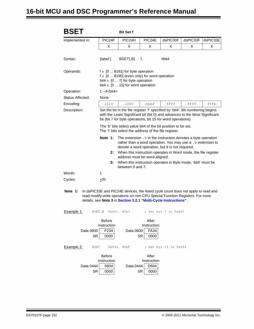
16-bit MCU and DSC Programmer’s Reference Manual
BSET Bit Set f
Implemented in: PIC24F PIC24H PIC24E dsPIC30F dsPIC33F dsPIC33E
X X X X X X
Syntax: {label:} BSET{.B} f, #bit4
Operands: f ∈ [0 ... 8191] for byte operationf ∈ [0 ... 8190] (even only) for word operationbit4 ∈ [0 ... 7] for byte operationbit4 ∈ [0 ... 15] for word operation
Operation: 1 → f<bit4>
Status Affected: None
Encoding: 1010 1000 bbbf ffff ffff fffb
Description: Set the bit in the file register ‘f’ specified by ‘bit4’. Bit numbering begins with the Least Significant bit (bit 0) and advances to the Most Significant bit (bit 7 for byte operations, bit 15 for word operations).
The ‘b’ bits select value bit4 of the bit position to be set.The ‘f’ bits select the address of the file register.
Note 1: The extension .B in the instruction denotes a byte operation rather than a word operation. You may use a .W extension to denote a word operation, but it is not required.
2: When this instruction operates in Word mode, the file register address must be word-aligned.
3: When this instruction operates in Byte mode, ‘bit4’ must be between 0 and 7.
Words: 1
Cycles: 1(1)
Note 1: In dsPIC33E and PIC24E devices, the listed cycle count does not apply to read and read-modify-write operations on non-CPU Special Function Registers. For more details, see Note 3 in Section 3.2.1 “Multi-Cycle Instructions”.
Example 1: BSET.B 0x601, #0x3 ; Set bit 3 in 0x601
Before Instruction
AfterInstruction
Data 0600 F234 Data 0600 FA34SR 0000 SR 0000
Example 2: BSET 0x444, #0xF ; Set bit 15 in 0x444
Before Instruction
AfterInstruction
Data 0444 5604 Data 0444 D604 SR 0000 SR 0000
DS70157F-page 152 © 2005-2011 Microchip Technology Inc.

Section 5. Instruction DescriptionsInstruction
Descriptions
5
BSET Bit Set in Ws
Implemented in: PIC24F PIC24H PIC24E dsPIC30F dsPIC33F dsPIC33E
X X X X X X
Syntax: {label:} BSET{.B} Ws, #bit4
[Ws],
[Ws++],
[Ws--],
[++Ws],
[--Ws],
Operands: Ws ∈ [W0 ... W15]bit4 ∈ [0 ... 7] for byte operationbit4 ∈ [0 ... 15] for word operation
Operation: 1 → Ws<bit4>
Status Affected: None
Encoding: 1010 0000 bbbb 0B00 0ppp ssss
Description: Set the bit in register Ws specified by ‘bit4’. Bit numbering begins with the Least Significant bit (bit 0) and advances to the Most Significant bit (bit 7 for byte operations, bit 15 for word operations). Register direct or indirect addressing may be used for Ws.
The ‘b’ bits select value bit4 of the bit position to be cleared.The ‘B’ bit selects byte or word operation (‘0’ for word, ‘1’ for byte).The ‘p’ bits select the source Address mode.The ‘s’ bits select the source/destination register.
Note 1: The extension .B in the instruction denotes a byte operation rather than a word operation. You may use a .W extension to denote a word operation, but it is not required.
2: When this instruction operates in Word mode, the source register address must be word-aligned.
3: When this instruction operates in Byte mode, ‘bit4’ must be between 0 and 7.
4: In dsPIC33E and PIC24E devices, this instruction uses the DSRPAG register for indirect address generation in Extended Data Space.
Words: 1
Cycles: 1(1)
Note 1: In dsPIC33E and PIC24E devices, the listed cycle count does not apply to read and read-modify-write operations on non-CPU Special Function Registers. For more details, see Note 3 in Section 3.2.1 “Multi-Cycle Instructions”.
© 2005-2011 Microchip Technology Inc. DS70157F-page 153

16-bit MCU and DSC Programmer’s Reference Manual
Example 1: BSET.B W3, #0x7 ; Set bit 7 in W3
Before Instruction
AfterInstruction
W3 0026 W3 00A6SR 0000 SR 0000
Example 2: BSET [W4++], #0x0 ; Set bit 0 in [W4]; Post-increment W4
Before Instruction
AfterInstruction
W4 6700 W4 6702Data 6700 1734 Data 6700 1735
SR 0000 SR 0000
DS70157F-page 154 © 2005-2011 Microchip Technology Inc.

Section 5. Instruction DescriptionsInstruction
Descriptions
5
BSW Bit Write in Ws
Implemented in: PIC24F PIC24H PIC24E dsPIC30F dsPIC33F dsPIC33E
X X X X X X
Syntax: {label:} BSW.C Ws, Wb
BSW.Z [Ws],
[Ws++],
[Ws--],
[++Ws],
[--Ws],
Operands: Ws ∈ [W0 ... W15]Wb ∈ [W0 ... W15]
Operation: For “.C” operation: C → Ws<(Wb)>For “.Z” operation (default): Z → Ws<(Wb)>
Status Affected: None
Encoding: 1010 1101 Zwww w000 0ppp ssss
Description: The (Wb) bit in register Ws is written with the value of the C or Z flag from the STATUS register. Bit numbering begins with the Least Significant bit (bit 0) and advances to the Most Significant bit (bit 15) of the working register. Only the four Least Significant bits of Wb are used to determine the destination bit number. Register direct addressing must be used for Wb, and either register direct, or indirect addressing may be used for Ws.
The ‘Z’ bit selects the C or Z flag as source.The ‘w’ bits select the address of the bit select register.The ‘p’ bits select the source Address mode.The ‘s’ bits select the source register.
Note: This instruction only operates in Word mode. If no extension is provided, the “.Z” operation is assumed.
Words: 1
Cycles: 1(1)
Note 1: In dsPIC33E and PIC24E devices, the listed cycle count does not apply to read and read-modify-write operations on non-CPU Special Function Registers. For more details, see Note 3 in Section 3.2.1 “Multi-Cycle Instructions”.
Example 1: BSW.C W2, W3 ; Set bit W3 in W2 to the value; of the C bit
Before Instruction
AfterInstruction
W2 F234 W2 7234W3 111F W3 111FSR 0002 (Z = 1, C = 0) SR 0002 (Z = 1, C = 0)
© 2005-2011 Microchip Technology Inc. DS70157F-page 155

16-bit MCU and DSC Programmer’s Reference Manual
Example 2: BSW.Z W2, W3 ; Set bit W3 in W2 to the complement; of the Z bit
Before Instruction
AfterInstruction
W2 E235 W2 E234W3 0550 W3 0550SR 0002 (Z = 1, C = 0) SR 0002 (Z = 1, C = 0)
Example 3: BSW.C [++W0], W6 ; Set bit W6 in [W0++] to the value; of the C bit
Before Instruction
AfterInstruction
W0 1000 W0 1002W6 34A3 W6 34A3
Data 1002 2380 Data 1002 2388SR 0001 (Z = 0, C = 1) SR 0001 (Z = 0, C = 1)
Example 4: BSW.Z [W1--], W5 ; Set bit W5 in [W1] to the; complement of the Z bit; Post-decrement W1
Before Instruction
AfterInstruction
W1 1000 W1 0FFEW5 888B W5 888B
Data 1000 C4DD Data 1000 CCDDSR 0001 (C = 1) SR 0001 (C = 1)
DS70157F-page 156 © 2005-2011 Microchip Technology Inc.

Section 5. Instruction DescriptionsInstruction
Descriptions
5
BTG Bit Toggle f
Implemented in: PIC24F PIC24H PIC24E dsPIC30F dsPIC33F dsPIC33E
X X X X X X
Syntax: {label:} BTG{.B} f, #bit4
Operands: f ∈ [0 ... 8191] for byte operationf ∈ [0 ... 8190] (even only) for word operationbit4 ∈ [0 ... 7] for byte operationbit4 ∈ [0 ... 15] for word operation
Operation: (f)<bit4> → (f)<bit4>
Status Affected: None
Encoding: 1010 1010 bbbf ffff ffff fffb
Description: Bit ‘bit4’ in file register ‘f’ is toggled (complemented). For the bit4 operand, bit numbering begins with the Least Significant bit (bit 0) and advances to the Most Significant bit (bit 7 for byte operation, bit 15 for word operation) of the byte.
The ‘b’ bits select value bit4, the bit position to toggle.The ‘f’ bits select the address of the file register.
Note 1: The extension .B in the instruction denotes a byte operation rather than a word operation. You may use a .W extension to denote a word operation, but it is not required.
2: When this instruction operates in Word mode, the file register address must be word-aligned.
3: When this instruction operates in Byte mode, ‘bit4’ must be between 0 and 7.
Words: 1
Cycles: 1(1)
Note 1: In dsPIC33E and PIC24E devices, the listed cycle count does not apply to read and read-modify-write operations on non-CPU Special Function Registers. For more details, see Note 3 in Section 3.2.1 “Multi-Cycle Instructions”.
Example 1: BTG.B 0x1001, #0x4 ; Toggle bit 4 in 0x1001
Before Instruction
AfterInstruction
Data 1000 F234 Data 1000 E234SR 0000 SR 0000
Example 2: BTG 0x1660, #0x8 ; Toggle bit 8 in RAM660
Before Instruction
AfterInstruction
Data 1660 5606 Data 1660 5706 SR 0000 SR 0000
© 2005-2011 Microchip Technology Inc. DS70157F-page 157

16-bit MCU and DSC Programmer’s Reference Manual
BTG Bit Toggle in Ws
Implemented in: PIC24F PIC24H PIC24E dsPIC30F dsPIC33F dsPIC33E
X X X X X X
Syntax: {label:} BTG{.B} Ws, #bit4
[Ws],
[Ws++],
[Ws--],
[++Ws],
[--Ws],
Operands: Ws ∈ [W0 ... W15]bit4 ∈ [0 ... 7] for byte operationbit4 ∈ [0 ... 15] for word operation
Operation: (Ws)<bit4> → Ws<bit4>
Status Affected: None
Encoding: 1010 0010 bbbb 0B00 0ppp ssss
Description: Bit ‘bit4’ in register Ws is toggled (complemented). For the bit4 operand, bit numbering begins with the Least Significant bit (bit 0) and advances to the Most Significant bit (bit 7 for byte operations, bit 15 for word operations). Register direct or indirect addressing may be used for Ws.
The ‘b’ bits select value bit4, the bit position to test.The ‘B’ bit selects byte or word operation (‘0’ for word, ‘1’ for byte).The ‘s’ bits select the source/destination register.The ‘p’ bits select the source Address mode.
Note 1: The extension .B in the instruction denotes a byte operation rather than a word operation. You may use a .W extension to denote a word operation, but it is not required.
2: When this instruction operates in Word mode, the source register address must be word-aligned.
3: When this instruction operates in Byte mode, ‘bit4’ must be between 0 and 7.
4: In dsPIC33E and PIC24E devices, this instruction uses the DSRPAG register for indirect address generation in Extended Data Space.
Words: 1
Cycles: 1(1)
Note 1: In dsPIC33E and PIC24E devices, the listed cycle count does not apply to read and read-modify-write operations on non-CPU Special Function Registers. For more details, see Note 3 in Section 3.2.1 “Multi-Cycle Instructions”.
Example 1: BTG W2, #0x0 ; Toggle bit 0 in W2
Before Instruction
AfterInstruction
W2 F234 W2 F235SR 0000 SR 0000
DS70157F-page 158 © 2005-2011 Microchip Technology Inc.

Section 5. Instruction DescriptionsInstruction
Descriptions
5
Example 2: BTG [W0++], #0x0 ; Toggle bit 0 in [W0]; Post-increment W0
Before Instruction
AfterInstruction
W0 2300 W0 2302Data 2300 5606 Data 2300 5607
SR 0000 SR 0000
© 2005-2011 Microchip Technology Inc. DS70157F-page 159

16-bit MCU and DSC Programmer’s Reference Manual
BTSC Bit Test f, Skip if Clear
Implemented in: PIC24F PIC24H PIC24E dsPIC30F dsPIC33F dsPIC33E
X X X X X X
Syntax: {label:} BTSC{.B} f, #bit4
Operands: f ∈ [0 ... 8191] for byte operationf ∈ [0 ... 8190] (even only) for word operationbit4 ∈ [0 ... 7] for byte operationbit4 ∈ [0 ... 15] for word operation
Operation: Test (f)<bit4>, skip if clear
Status Affected: None
Encoding: 1010 1111 bbbf ffff ffff fffb
Description: Bit ‘bit4’ in the file register is tested. If the tested bit is ‘0’, the next instruction (fetched during the current instruction execution) is discarded and on the next cycle, a NOP is executed instead. If the tested bit is ‘1’, the next instruction is executed as normal. In either case, the contents of the file register are not changed. For the bit4 operand, bit numbering begins with the Least Significant bit (bit 0) and advances to the Most Significant bit (bit 7 for byte operations, bit 15 for word operations).
The ‘b’ bits select value bit4, the bit position to test.The ‘f’ bits select the address of the file register.
Note 1: The extension .B in the instruction denotes a byte operation rather than a word operation. You may use a .W extension to denote a word operation, but it is not required.
2: When this instruction operates in Word mode, the file register address must be word-aligned.
3: When this instruction operates in Byte mode, ‘bit4’ must be between 0 and 7.
Words: 1
Cycles: 1 (2 or 3)(1)
Note 1: In dsPIC33E and PIC24E devices, the listed cycle count does not apply to read and read-modify-write operations on non-CPU Special Function Registers. For more details, see Note 3 in Section 3.2.1 “Multi-Cycle Instructions”.
Example 1: 002000 HERE: BTSC.B 0x1201, #2002002 GOTO BYPASS002004 . . .002006 . . .002008 BYPASS: . . .00200A . . .
; If bit 2 of 0x1201 is 0,; skip the GOTO
Before Instruction
After Instruction
PC 00 2000 PC 00 2002Data 1200 264F Data 1200 264F
SR 0000 SR 0000
DS70157F-page 160 © 2005-2011 Microchip Technology Inc.

Section 5. Instruction DescriptionsInstruction
Descriptions
5
Example 2: 002000 HERE: BTSC 0x804, #14002002 GOTO BYPASS002004 . . .002006 . . .002008 BYPASS: . . .00200A . . .
; If bit 14 of 0x804 is 0,; skip the GOTO
Before Instruction
After Instruction
PC 00 2000 PC 00 2006Data 0804 2647 Data 0804 2647
SR 0000 SR 0000
© 2005-2011 Microchip Technology Inc. DS70157F-page 161

16-bit MCU and DSC Programmer’s Reference Manual
BTSC Bit Test Ws, Skip if Clear
Implemented in: PIC24F PIC24H PIC24E dsPIC30F dsPIC33F dsPIC33E
X X X X X X
Syntax: {label:} BTSC Ws, #bit4
[Ws],
[Ws++],
[Ws--],
[++Ws],
[--Ws],
Operands: Ws ∈ [W0 ... W15]bit4 ∈ [0 ... 15]
Operation: Test (Ws)<bit4>, skip if clear
Status Affected: None
Encoding: 1010 0111 bbbb 0000 0ppp ssss
Description: Bit ‘bit4’ in Ws is tested. If the tested bit is ‘0’, the next instruction (fetched during the current instruction execution) is discarded and on the next cycle, a NOP is executed instead. If the tested bit is ‘1’, the next instruction is executed as normal. In either case, the contents of Ws are not changed. For the bit4 operand, bit numbering begins with the Least Significant bit (bit 0) and advances to the Most Significant bit (bit 15) of the word. Either register direct or indirect addressing may be used for Ws.
The ‘b’ bits select value bit4, the bit position to test.The ‘p’ bits select the source Address mode.The ‘s’ bits select the source register.
Note: This instruction operates in Word mode only.
Words: 1
Cycles: 1 (2 or 3 if the next instruction is skipped)(1)
Note 1: In dsPIC33E and PIC24E devices, the listed cycle count does not apply to read and read-modify-write operations on non-CPU Special Function Registers. For more details, see Note 3 in Section 3.2.1 “Multi-Cycle Instructions”.
Example 1: 002000 HERE: BTSC W0, #0x0002002 GOTO BYPASS002004 . . .002006 . . .002008 BYPASS: . . .00200A . . .
; If bit 0 of W0 is 0,; skip the GOTO
Before Instruction
After Instruction
PC 00 2000 PC 00 2002W0 264F W0 264FSR 0000 SR 0000
DS70157F-page 162 © 2005-2011 Microchip Technology Inc.

Section 5. Instruction DescriptionsInstruction
Descriptions
5
Example 2: 002000 HERE: BTSC W6, #0xF002002 GOTO BYPASS002004 . . .002006 . . .002008 BYPASS: . . .00200A . . .
; If bit 15 of W6 is 0,; skip the GOTO
Before Instruction
After Instruction
PC 00 2000 PC 00 2006W6 264F W6 264FSR 0000 SR 0000
Example 3: 003400 HERE: BTSC [W6++], #0xC003402 GOTO BYPASS003404 . . .003406 . . .003408 BYPASS: . . .00340A . . .
; If bit 12 of [W6] is 0,; skip the GOTO; Post-increment W6
Before Instruction
After Instruction
PC 00 3400 PC 00 3402W6 1800 W6 1802
Data 1800 1000 Data 1800 1000SR 0000 SR 0000
© 2005-2011 Microchip Technology Inc. DS70157F-page 163

16-bit MCU and DSC Programmer’s Reference Manual
BTSS Bit Test f, Skip if Set
Implemented in: PIC24F PIC24H PIC24E dsPIC30F dsPIC33F dsPIC33E
X X X X X X
Syntax: {label:} BTSS{.B} f, #bit4
Operands: f ∈ [0 ... 8191] for byte operationf ∈ [0 ... 8190] (even only) for word operationbit4 ∈ [0 ... 7] for byte operationbit4 ∈ [0 ... 15] for word operation
Operation: Test (f)<bit4>, skip if set
Status Affected: None
Encoding: 1010 1110 bbbf ffff ffff fffb
Description: Bit ‘bit4’ in the file register ‘f’ is tested. If the tested bit is ‘1’, the next instruction (fetched during the current instruction execution) is discarded and on the next cycle, a NOP is executed instead. If the tested bit is ‘0’, the next instruction is executed as normal. In either case, the contents of the file register are not changed. For the bit4 operand, bit numbering begins with the Least Significant bit (bit 0) and advances to the Most Significant bit (bit 7 for byte operation, bit 15 for word operation).
The ‘b’ bits select value bit4, the bit position to test.The ‘f’ bits select the address of the file register.
Note 1: The extension .B in the instruction denotes a byte operation rather than a word operation. You may use a .W extension to denote a word operation, but it is not required.
2: When this instruction operates in Word mode, the file register address must be word-aligned.
3: When this instruction operates in Byte mode, ‘bit4’ must be between 0 and 7.
Words: 1
Cycles: 1 (2 or 3 if the next instruction is skipped)(1)
Note 1: In dsPIC33E and PIC24E devices, the listed cycle count does not apply to read and read-modify-write operations on non-CPU Special Function Registers. For more details, see Note 3 in Section 3.2.1 “Multi-Cycle Instructions”.
DS70157F-page 164 © 2005-2011 Microchip Technology Inc.

Section 5. Instruction DescriptionsInstruction
Descriptions
5
Example 1: 007100 HERE: BTSS.B 0x1401, #0x1007102 CLR WREG007104 . . .
; If bit 1 of 0x1401 is 1,; don’t clear WREG
Before Instruction
After Instruction
PC 00 7100 PC 00 7104Data 1400 0280 Data 1400 0280
SR 0000 SR 0000
Example 2: 007100 HERE: BTSS 0x890, #0x9007102 GOTO BYPASS007104 . . .007106 BYPASS: . . .
; If bit 9 of 0x890 is 1,; skip the GOTO
Before Instruction
After Instruction
PC 00 7100 PC 00 7102Data 0890 00FE Data 0890 00FE
SR 0000 SR 0000
© 2005-2011 Microchip Technology Inc. DS70157F-page 165

16-bit MCU and DSC Programmer’s Reference Manual
BTSS Bit Test Ws, Skip if Set
Implemented in: PIC24F PIC24H PIC24E dsPIC30F dsPIC33F dsPIC33E
X X X X X X
Syntax: {label:} BTSS Ws, #bit4
[Ws],
[Ws++],
[Ws--],
[++Ws],
[--Ws],
Operands: Ws ∈ [W0 ... W15]bit4 ∈ [0 ... 15]
Operation: Test (Ws)<bit4>, skip if set.
Status Affected: None
Encoding: 1010 0110 bbbb 0000 0ppp ssss
Description: Bit ‘bit4’ in Ws is tested. If the tested bit is ‘1’, the next instruction (fetched during the current instruction execution) is discarded and on the next cycle, a NOP is executed instead. If the tested bit is ‘0’, the next instruction is executed as normal. In either case, the contents of Ws are not changed. For the bit4 operand, bit numbering begins with the Least Significant bit (bit 0) and advances to the Most Significant bit (bit 15) of the word. Either register direct or indirect addressing may be used for Ws.
The ‘b’ bits select the value bit4, the bit position to test.The ‘s’ bits select the source register.The ‘p’ bits select the source Address mode.
Note: This instruction operates in Word mode only.
Words: 1
Cycles: 1 (2 or 3 if the next instruction is skipped)(1)
Note 1: In dsPIC33E and PIC24E devices, the listed cycle count does not apply to read and read-modify-write operations on non-CPU Special Function Registers. For more details, see Note 3 in Section 3.2.1 “Multi-Cycle Instructions”.
Example 1: 002000 HERE: BTSS W0, #0x0002002 GOTO BYPASS002004 . . .002006 . . .002008 BYPASS: . . .00200A . . .
; If bit 0 of W0 is 1,; skip the GOTO
Before Instruction
After Instruction
PC 00 2000 PC 00 2006W0 264F W0 264FSR 0000 SR 0000
DS70157F-page 166 © 2005-2011 Microchip Technology Inc.

Section 5. Instruction DescriptionsInstruction
Descriptions
5
Example 2: 002000 HERE: BTSS W6, #0xF002002 GOTO BYPASS002004 . . .002006 . . .002008 BYPASS: . . .00200A . . .
; If bit 15 of W6 is 1,; skip the GOTO
Before Instruction
After Instruction
PC 00 2000 PC 00 2002W6 264F W6 264FSR 0000 SR 0000
Example 3: 003400 HERE: BTSS [W6++], 0xC003402 GOTO BYPASS003404 . . .003406 . . .003408 BYPASS: . . .00340A . . .
; If bit 12 of [W6] is 1,; skip the GOTO; Post-increment W6
Before Instruction
After Instruction
PC 00 3400 PC 00 3406W6 1800 W6 1802
Data 1800 1000 Data 1800 1000SR 0000 SR 0000
© 2005-2011 Microchip Technology Inc. DS70157F-page 167

16-bit MCU and DSC Programmer’s Reference Manual
BTST Bit Test f
Implemented in: PIC24F PIC24H PIC24E dsPIC30F dsPIC33F dsPIC33E
X X X X X X
Syntax: {label:} BTST{.B} f, #bit4
Operands: f ∈ [0 ... 8191] for byte operationf ∈ [0 ... 8190] (even only) for word operationbit4 ∈ [0 ... 7] for byte operationbit4 ∈ [0 ... 15] for word operation
Operation: (f)<bit4> → Z
Status Affected: Z
Encoding: 1010 1011 bbbf ffff ffff fffb
Description: Bit ‘bit4’ in file register ‘f’ is tested and the complement of the tested bit is stored to the Z flag in the STATUS register. The contents of the file register are not changed. For the bit4 operand, bit numbering begins with the Least Significant bit (bit 0) and advances to the Most Significant bit (bit 7 for byte operation, bit 15 for word operation).
The ‘b’ bits select value bit4, the bit position to be tested.The ‘f’ bits select the address of the file register.
Note 1: The extension .B in the instruction denotes a byte operation rather than a word operation. You may use a .W extension to denote a word operation, but it is not required.
2: When this instruction operates in Word mode, the file register address must be word-aligned.
3: When this instruction operates in Byte mode, ‘bit4’ must be between 0 and 7.
Words: 1
Cycles: 1(1)
Note 1: In dsPIC33E and PIC24E devices, the listed cycle count does not apply to read and read-modify-write operations on non-CPU Special Function Registers. For more details, see Note 3 in Section 3.2.1 “Multi-Cycle Instructions”.
Example 1: BTST.B 0x1201, #0x3 ; Set Z = complement of ; bit 3 in 0x1201
Before Instruction
AfterInstruction
Data 1200 F7FF Data 1200 F7FFSR 0000 SR 0002 (Z = 1)
Example 2: BTST 0x1302, #0x7 ; Set Z = complement of; bit 7 in 0x1302
Before Instruction
AfterInstruction
Data 1302 F7FF Data 1302 F7FFSR 0002 (Z = 1) SR 0000
DS70157F-page 168 © 2005-2011 Microchip Technology Inc.

Section 5. Instruction DescriptionsInstruction
Descriptions
5
BTST Bit Test in Ws
Implemented in: PIC24F PIC24H PIC24E dsPIC30F dsPIC33F dsPIC33E
X X X X X X
Syntax: {label:} BTST.C Ws, #bit4
BTST.Z [Ws],
[Ws++],
[Ws--],
[++Ws],
[--Ws],
Operands: Ws ∈ [W0 ... W15]bit4 ∈ [0 ... 15]
Operation: For “.C” operation: (Ws)<bit4> → C For “.Z” operation (default): (Ws)<bit4> → Z
Status Affected: Z or C
Encoding: 1010 0011 bbbb Z000 0ppp ssss
Description: Bit ‘bit4’ in register Ws is tested. If the “.Z” option of the instruction is specified, the complement of the tested bit is stored to the Zero flag in the STATUS register. If the “.C” option of the instruction is specified, the value of the tested bit is stored to the Carry flag in the STATUS register. In either case, the contents of Ws are not changed.
For the bit4 operand, bit numbering begins with the Least Significant bit (bit 0) and advances to the Most Significant bit (bit 15) of the word. Either register direct or indirect addressing may be used for Ws.The ‘b’ bits select value bit4, the bit position to test.The ‘Z’ bit selects the C or Z flag as destination.The ‘p’ bits select the source Address mode.The ‘s’ bits select the source register.
Note: This instruction only operates in Word mode. If no extension is provided, the “.Z” operation is assumed.
Words: 1
Cycles: 1(1)
Note 1: In dsPIC33E and PIC24E devices, the listed cycle count does not apply to read and read-modify-write operations on non-CPU Special Function Registers. For more details, see Note 3 in Section 3.2.1 “Multi-Cycle Instructions”.
© 2005-2011 Microchip Technology Inc. DS70157F-page 169
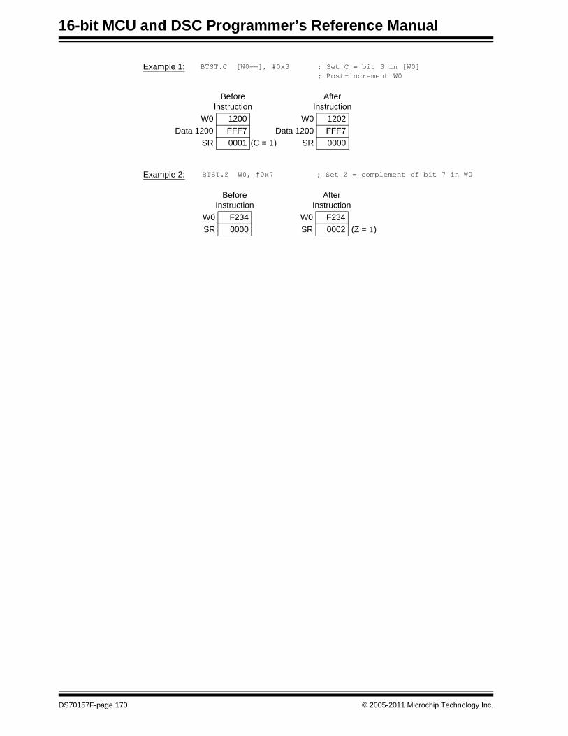
16-bit MCU and DSC Programmer’s Reference Manual
Example 1: BTST.C [W0++], #0x3 ; Set C = bit 3 in [W0]; Post-increment W0
Before Instruction
AfterInstruction
W0 1200 W0 1202Data 1200 FFF7 Data 1200 FFF7
SR 0001 (C = 1) SR 0000
Example 2: BTST.Z W0, #0x7 ; Set Z = complement of bit 7 in W0
Before Instruction
AfterInstruction
W0 F234 W0 F234SR 0000 SR 0002 (Z = 1)
DS70157F-page 170 © 2005-2011 Microchip Technology Inc.
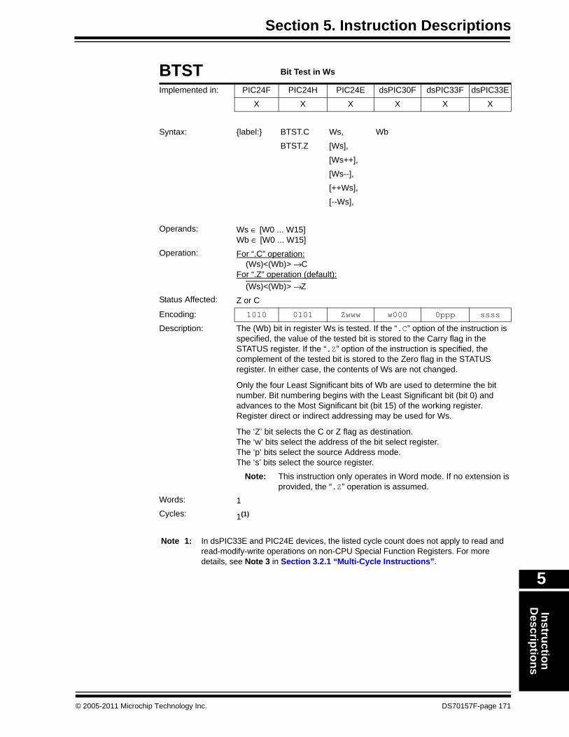
Section 5. Instruction DescriptionsInstruction
Descriptions
5
BTST Bit Test in Ws
Implemented in: PIC24F PIC24H PIC24E dsPIC30F dsPIC33F dsPIC33E
X X X X X X
Syntax: {label:} BTST.C Ws, Wb
BTST.Z [Ws],
[Ws++],
[Ws--],
[++Ws],
[--Ws],
Operands: Ws ∈ [W0 ... W15]Wb ∈ [W0 ... W15]
Operation: For “.C” operation: (Ws)<(Wb)> → C For “.Z” operation (default): (Ws)<(Wb)> → Z
Status Affected: Z or C
Encoding: 1010 0101 Zwww w000 0ppp ssss
Description: The (Wb) bit in register Ws is tested. If the “.C” option of the instruction is specified, the value of the tested bit is stored to the Carry flag in the STATUS register. If the “.Z” option of the instruction is specified, the complement of the tested bit is stored to the Zero flag in the STATUS register. In either case, the contents of Ws are not changed.
Only the four Least Significant bits of Wb are used to determine the bit number. Bit numbering begins with the Least Significant bit (bit 0) and advances to the Most Significant bit (bit 15) of the working register. Register direct or indirect addressing may be used for Ws.
The ‘Z’ bit selects the C or Z flag as destination.The ‘w’ bits select the address of the bit select register.The ‘p’ bits select the source Address mode.The ‘s’ bits select the source register.
Note: This instruction only operates in Word mode. If no extension is provided, the “.Z” operation is assumed.
Words: 1Cycles: 1(1)
Note 1: In dsPIC33E and PIC24E devices, the listed cycle count does not apply to read and read-modify-write operations on non-CPU Special Function Registers. For more details, see Note 3 in Section 3.2.1 “Multi-Cycle Instructions”.
© 2005-2011 Microchip Technology Inc. DS70157F-page 171

16-bit MCU and DSC Programmer’s Reference Manual
Example 1: BTST.C W2, W3 ; Set C = bit W3 of W2
Before Instruction
AfterInstruction
W2 F234 W2 F234W3 2368 W3 2368SR 0001 (C = 1) SR 0000
Example 2: BTST.Z [W0++], W1 ; Set Z = complement of ; bit W1 in [W0], ; Post-increment W0
Before Instruction
AfterInstruction
W0 1200 W0 1202W1 CCC0 W1 CCC0
Data 1200 6243 Data 1200 6243SR 0002 (Z = 1) SR 0000
DS70157F-page 172 © 2005-2011 Microchip Technology Inc.

Section 5. Instruction DescriptionsInstruction
Descriptions
5
BTSTS Bit Test/Set f
Implemented in: PIC24F PIC24H PIC24E dsPIC30F dsPIC33F dsPIC33E
X X X X X X
Syntax: {label:} BTSTS{.B} f, #bit4
Operands: f ∈ [0 ... 8191] for byte operationf ∈ [0 ... 8190] (even only) for word operationbit4 ∈ [0 ... 7] for byte operationbit4 ∈ [0 ... 15] for word operation
Operation: (f)<bit4> → Z1 → (f)<bit4>
Status Affected: Z
Encoding: 1010 1100 bbbf ffff ffff fffb
Description: Bit ‘bit4’ in file register ‘f’ is tested and the complement of the tested bit is stored to the Zero flag in the STATUS register. The tested bit is then set to ‘1’ in the file register. For the bit4 operand, bit numbering begins with the Least Significant bit (bit 0) and advances to the Most Significant bit (bit 7 for byte operations, bit 15 for word operations).
The ‘b’ bits select value bit4, the bit position to test/set.The ‘f’ bits select the address of the file register.
Note 1: The extension .B in the instruction denotes a byte operation rather than a word operation. You may use a .W extension to denote a word operation, but it is not required.
2: When this instruction operates in Word mode, the file register address must be word-aligned.
3: When this instruction operates in Byte mode, ‘bit4’ must be between 0 and 7.
4: The file register ‘f’ must not be the CPU Status register (SR).
Words: 1
Cycles: 1(1)
Note 1: In dsPIC33E and PIC24E devices, the listed cycle count does not apply to read and read-modify-write operations on non-CPU Special Function Registers. For more details, see Note 3 in Section 3.2.1 “Multi-Cycle Instructions”.
© 2005-2011 Microchip Technology Inc. DS70157F-page 173
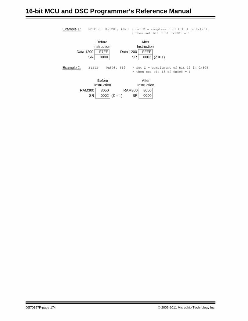
16-bit MCU and DSC Programmer’s Reference Manual
Example 1: BTSTS.B 0x1201, #0x3 ; Set Z = complement of bit 3 in 0x1201, ; then set bit 3 of 0x1201 = 1
Before Instruction
AfterInstruction
Data 1200 F7FF Data 1200 FFFFSR 0000 SR 0002 (Z = 1)
Example 2: BTSTS 0x808, #15 ; Set Z = complement of bit 15 in 0x808,; then set bit 15 of 0x808 = 1
Before Instruction
AfterInstruction
RAM300 8050 RAM300 8050SR 0002 (Z = 1) SR 0000
DS70157F-page 174 © 2005-2011 Microchip Technology Inc.

Section 5. Instruction DescriptionsInstruction
Descriptions
5
BTSTS Bit Test/Set in Ws
Implemented in: PIC24F PIC24H PIC24E dsPIC30F dsPIC33F dsPIC33EX X X X X X
Syntax: {label:} BTSTS.C Ws, #bit4BTSTS.Z [Ws],
[Ws++],[Ws--],[++Ws],[--Ws],
Operands: Ws ∈ [W0 ... W15]bit4 ∈ [0 ... 15]
Operation: For “.C” operation: (Ws)<bit4> → C 1 → Ws<bit4>For “.Z” operation (default): (Ws)<bit4> → Z 1 → Ws<bit4>
Status Affected: Z or CEncoding: 1010 0100 bbbb Z000 0ppp ssss
Description: Bit ‘bit4’ in register Ws is tested. If the “.Z” option of the instruction is specified, the complement of the tested bit is stored to the Zero flag in the STATUS register. If the “.C” option of the instruction is specified, the value of the tested bit is stored to the Carry flag in the STATUS register. In both cases, the tested bit in Ws is set to ‘1’.
The ‘b’ bits select the value bit4, the bit position to test/set.The ‘Z’ bit selects the C or Z flag as destination.The ‘p’ bits select the source Address mode.The ‘s’ bits select the source register.Note 1: This instruction only operates in Word mode. If no extension is
provided, the “.Z” operation is assumed.2: If Ws is used as a pointer, it must not contain the address of the
CPU Status register (SR).3: In dsPIC33E and PIC24E devices, this instruction uses the
DSRPAG register for indirect address generation in Extended Data Space.
Words: 1Cycles: 1(1)
Note 1: In dsPIC33E and PIC24E devices, the listed cycle count does not apply to read and read-modify-write operations on non-CPU Special Function Registers. For more details, see Note 3 in Section 3.2.1 “Multi-Cycle Instructions”.
© 2005-2011 Microchip Technology Inc. DS70157F-page 175

16-bit MCU and DSC Programmer’s Reference Manual
Example 1: BTSTS.C [W0++], #0x3 ; Set C = bit 3 in [W0] ; Set bit 3 in [W0] = 1; Post-increment W0
Before Instruction
AfterInstruction
W0 1200 W0 1202Data 1200 FFF7 Data 1200 FFFF
SR 0001 (C = 1) SR 0000
Example 2: BTSTS.Z W0, #0x7 ; Set Z = complement of bit 7 ; in W0, and set bit 7 in W0 = 1
Before Instruction
AfterInstruction
W0 F234 W0 F2BCSR 0000 SR 0002 (Z = 1)
DS70157F-page 176 © 2005-2011 Microchip Technology Inc.

Section 5. Instruction DescriptionsInstruction
Descriptions
5
CALL Call Subroutine
Implemented in: PIC24F PIC24H PIC24E dsPIC30F dsPIC33F dsPIC33EX X X X
Syntax: {label:} CALL Expr
Operands: Expr may be a label or expression (but not a literal).Expr is resolved by the linker to a lit23, where lit23 ∈ [0 ... 8388606].
Operation: (PC) + 4 → PC(PC<15:0>) → (TOS)(W15) + 2 → W15(PC<23:16>) → (TOS)(W15) + 2 → W15lit23 → PC NOP → Instruction Register
Status Affected: NoneEncoding: 1st word 0000 0010 nnnn nnnn nnnn nnn0 2nd word 0000 0000 0000 0000 0nnn nnnnDescription: Direct subroutine call over the entire 4-Mbyte instruction program
memory range. Before the CALL is made, the 24-bit return address (PC + 4) is PUSHed onto the stack. After the return address is stacked, the 23-bit value ‘lit23’ is loaded into the PC.
The ‘n’ bits form the target address.
Note: The linker will resolve the specified expression into the lit23 to be used.
Words: 2Cycles: 2
Example 1: 026000 CALL _FIR026004 MOV W0, W1 . ... . ...026844 _FIR: MOV #0x400, W2026846 ...
; Call _FIR subroutine
; _FIR subroutine start
Before Instruction
After Instruction
PC 02 6000 PC 02 6844W15 A268 W15 A26C
Data A268 FFFF Data A268 6004Data A26A FFFF Data A26A 0002
SR 0000 SR 0000
© 2005-2011 Microchip Technology Inc. DS70157F-page 177

16-bit MCU and DSC Programmer’s Reference Manual
Example 2: 072000 CALL _G66 ; call routine _G66072004 MOV W0, W1 . ...077A28 _G66: INC W6, [W7++] ; routine start077A2A ...077A2C
Before Instruction
After Instruction
PC 07 2000 PC 07 7A28W15 9004 W15 9008
Data 9004 FFFF Data 9004 2004Data 9006 FFFF Data 9006 0007
SR 0000 SR 0000
CALL Call Subroutine
Implemented in: PIC24F PIC24H PIC24E dsPIC30F dsPIC33F dsPIC33EX X
Syntax: {label:} CALL Expr
Operands: Expr may be a label or expression (but not a literal).Expr is resolved by the linker to a lit23, where lit23 ∈ [0 ... 8388606].
Operation: (PC) + 4 → PC(PC<15:1>) → TOS<15:1>, SFA bit → TOS<0>(W15) + 2 → W15(PC<23:16>) → TOS(W15) + 2 → W150 → SFA bitlit23 → PC NOP → Instruction Register
Status Affected: SFAEncoding: 1st word 0000 0010 nnnn nnnn nnnn nnn0 2nd word 0000 0000 0000 0000 0nnn nnnnDescription: Direct subroutine call over the entire 4-Mbyte instruction program
memory range. Before the CALL is made, the 24-bit return address (PC + 4) is PUSHed onto the stack. After the return address is stacked, the 23-bit value ‘lit23’ is loaded into the PC.
The ‘n’ bits form the target address.
Note: The linker will resolve the specified expression into the lit23 to be used.
Words: 2Cycles: 4
DS70157F-page 178 © 2005-2011 Microchip Technology Inc.

Section 5. Instruction DescriptionsInstruction
Descriptions
5
Example 1: 026000 CALL _FIR026004 MOV W0, W1 . ... . ...026844 _FIR: MOV #0x400, W2026846 ...
; Call _FIR subroutine
; _FIR subroutine start
Before Instruction
After Instruction
PC 02 6000 PC 02 6844W15 A268 W15 A26C
Data A268 FFFF Data A268 6004Data A26A FFFF Data A26A 0002
SR 0000 SR 0000
Example 2: 072000 CALL _G66 ; call routine _G66072004 MOV W0, W1 . ...077A28 _G66: INC W6, [W7++] ; routine start077A2A ...077A2C
Before Instruction
After Instruction
PC 07 2000 PC 07 7A28W15 9004 W15 9008
Data 9004 FFFF Data 9004 2004Data 9006 FFFF Data 9006 0007
SR 0000 SR 0000
© 2005-2011 Microchip Technology Inc. DS70157F-page 179
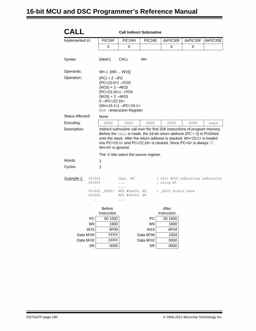
16-bit MCU and DSC Programmer’s Reference Manual
CALL Call Indirect Subroutine
Implemented in: PIC24F PIC24H PIC24E dsPIC30F dsPIC33F dsPIC33E
X X X X
Syntax: {label:} CALL Wn
Operands: Wn ∈ [W0 ... W15]Operation: (PC) + 2 → PC
(PC<15:0>) → TOS(W15) + 2 → W15(PC<23:16>) → TOS(W15) + 2 → W150 → PC<22:16>(Wn<15:1>) → PC<15:1>NOP → Instruction Register
Status Affected: None
Encoding: 0000 0001 0000 0000 0000 ssss
Description: Indirect subroutine call over the first 32K instructions of program memory. Before the CALL is made, the 24-bit return address (PC + 2) is PUSHed onto the stack. After the return address is stacked, Wn<15:1> is loaded into PC<15:1> and PC<22:16> is cleared. Since PC<0> is always ‘0’, Wn<0> is ignored.
The ‘s’ bits select the source register.Words: 1Cycles: 2
Example 1: 001002 CALL W0001004 ... . ...001600 _BOOT: MOV #0x400, W2001602 MOV #0x300, W6 . ...
; Call BOOT subroutine indirectly; using W0
; _BOOT starts here
Before Instruction
After Instruction
PC 00 1002 PC 00 1600W0 1600 W0 1600
W15 6F00 W15 6F04Data 6F00 FFFF Data 6F00 1004Data 6F02 FFFF Data 6F02 0000
SR 0000 SR 0000
DS70157F-page 180 © 2005-2011 Microchip Technology Inc.

Section 5. Instruction DescriptionsInstruction
Descriptions
5
Example 2: 004200 CALL W7004202 ... . ...005500 _TEST: INC W1, W2005502 DEC W1, W3 . ...
; Call TEST subroutine indirectly; using W7
; _TEST starts here;
Before Instruction
After Instruction
PC 00 4200 PC 00 5500W7 5500 W7 5500
W15 6F00 W15 6F04Data 6F00 FFFF Data 6F00 4202Data 6F02 FFFF Data 6F02 0000
SR 0000 SR 0000
CALL Call Indirect Subroutine
Implemented in: PIC24F PIC24H PIC24E dsPIC30F dsPIC33F dsPIC33E
X X
Syntax: {label:} CALL Wn
Operands: Wn ∈ [W0 ... W15]Operation: (PC) + 2 → PC
(PC<15:1>) → TOS, SFA bit → TOS<0>(W15) + 2 → W15(PC<23:16>) → TOS(W15) + 2 → W150 → SFA bit0 → PC<22:16>(Wn<15:1>) → PC<15:1>NOP → Instruction Register
Status Affected: SFA
Encoding: 0000 0001 0000 0000 0000 ssss
Description: Indirect subroutine call over the first 32K instructions of program memory. Before the CALL is made, the 24-bit return address (PC + 2) is PUSHed onto the stack. After the return address is stacked, Wn<15:1> is loaded into PC<15:1> and PC<22:16> is cleared. Since PC<0> is always ‘0’, Wn<0> is ignored.
The ‘s’ bits select the source register.Words: 1Cycles: 4
© 2005-2011 Microchip Technology Inc. DS70157F-page 181

16-bit MCU and DSC Programmer’s Reference Manual
Example 1: 001002 CALL W0001004 ... . ...001600 _BOOT: MOV #0x400, W2001602 MOV #0x300, W6 . ...
; Call BOOT subroutine indirectly; using W0
; _BOOT starts here
Before Instruction
After Instruction
PC 00 1002 PC 00 1600W0 1600 W0 1600
W15 6F00 W15 6F04Data 6F00 FFFF Data 6F00 1004Data 6F02 FFFF Data 6F02 0000
SR 0000 SR 0000
Example 2: 004200 CALL W7004202 ... . ...005500 _TEST: INC W1, W2005502 DEC W1, W3 . ...
; Call TEST subroutine indirectly; using W7
; _TEST starts here;
Before Instruction
After Instruction
PC 00 4200 PC 00 5500W7 5500 W7 5500
W15 6F00 W15 6F04Data 6F00 FFFF Data 6F00 4202Data 6F02 FFFF Data 6F02 0000
SR 0000 SR 0000
DS70157F-page 182 © 2005-2011 Microchip Technology Inc.

Section 5. Instruction DescriptionsInstruction
Descriptions
5
CALL.L Call Indirect Subroutine Long
Implemented in: PIC24F PIC24H PIC24E dsPIC30F dsPIC33F dsPIC33EX X
Syntax: {label:} CALL.L Wn
Operands: Wn ∈ [W0, W2, W4, W6, W8, W10, W12]Operation: (PC) +2 → PC,
(PC<15:1>) → TOS<15:1>, SFA bit → TOS<0>(W15)+2 → W15(PC<23:16>) → TOS,(W15)+2 → W150 → SFA bit,PC<23> → PC<23> (see text); (Wn+1)<6:0> → PC<22:16>; (Wn) → PC<15:0>NOP → Instruction Register
Status Affected: SFAEncoding: 0000 0001 1www w000 0000 ssssDescription: Indirect subroutine call to any User program memory address. First, return
address (PC+2) and the state of the Stack Frame Active bit (SFA) is pushed onto the system stack, after which the SFA bit is cleared.Then, the LS 7-bits of (Wn+1) are loaded in PC<22:16>, and the 16-bitvalue (Wn) is loaded into PC<15:0>. PC<23> is not modified by this instruction.The contents of (Wn+1)<15:7> are ignored.The value of Wn<0> is also ignored and PC<0> is always set to 0.The ‘s’ bits specify the address of the Wn source register.The ‘w’ bits specify the address of the Wn+1 source register.
Words: 1Cycles: 4
Example 1: 026000 CALL.L W4026004 MOV W0, W1 . ... . ...026844 _FIR: MOV #0x400, W2026846 ...
; Call _FIR subroutine
; _FIR subroutine start
Before Instruction
After Instruction
PC 02 6000 PC 02 6844W4 6844 W4 6844W5 0002 W5 0002
W15 A268 W15 A26CData A268 FFFF Data A268 6004Data A26A FFFF Data A26A 0002
SR 0000 SR 0000
© 2005-2011 Microchip Technology Inc. DS70157F-page 183

16-bit MCU and DSC Programmer’s Reference Manual
CLR Clear f or WREG
Implemented in: PIC24F PIC24H PIC24E dsPIC30F dsPIC33F dsPIC33E
X X X X X X
Syntax: {label:} CLR{.B} f
WREG
Operands: f ∈ [0 ... 8191]
Operation: 0 → destination designated by D
Status Affected: None
Encoding: 1110 1111 0BDf ffff ffff ffff
Description: Clear the contents of a file register or the default working register WREG. If WREG is specified, the WREG is cleared. Otherwise, the specified file register ‘f’ is cleared.
The ‘B’ bit selects byte or word operation (‘0’ for word, ‘1’ for byte).The ‘D’ bit selects the destination (‘0’ for WREG, ‘1’ for file register).The ‘f’ bits select the address of the file register.
Note 1: The extension .B in the instruction denotes a byte operation rather than a word operation. You may use a .W extension to denote a word operation, but it is not required.
2: The WREG is set to working register W0.
Words: 1
Cycles: 1Example 1: CLR.B RAM200 ; Clear RAM200 (Byte mode)
Before Instruction
AfterInstruction
RAM200 8009 RAM200 8000SR 0000 SR 0000
Example 2: CLR WREG ; Clear WREG (Word mode)
Before Instruction
AfterInstruction
WREG 0600 WREG 0000SR 0000 SR 0000
DS70157F-page 184 © 2005-2011 Microchip Technology Inc.

Section 5. Instruction DescriptionsInstruction
Descriptions
5
CLR Clear Wd
Implemented in: PIC24F PIC24H PIC24E dsPIC30F dsPIC33F dsPIC33E
X X X X X X
Syntax: {label:} CLR{.B} Wd
[Wd]
[Wd++]
[Wd--]
[++Wd]
[--Wd]
Operands: Wd ∈ [W0 ... W15]
Operation: 0 → Wd
Status Affected: None
Encoding: 1110 1011 0Bqq qddd d000 0000
Description: Clear the contents of register Wd. Either register direct or indirect addressing may be used for Wd.
The ‘B’ bit select byte or word operation (‘0’ for word, ‘1’ for byte).The ‘q’ bits select the destination Address mode.The ‘d’ bits select the destination register.
Note: The extension .B in the instruction denotes a byte operation rather than a word operation. You may use a .W extension to denote a word operation, but it is not required.
Words: 1
Cycles: 1
Example 1: CLR.B W2 ; Clear W2 (Byte mode)
Before Instruction
AfterInstruction
W2 3333 W2 3300SR 0000 SR 0000
Example 2: CLR [W0++] ; Clear [W0] ; Post-increment W0
Before Instruction
AfterInstruction
W0 2300 W0 2302Data 2300 5607 Data 2300 0000
SR 0000 SR 0000
© 2005-2011 Microchip Technology Inc. DS70157F-page 185

16-bit MCU and DSC Programmer’s Reference Manual
CLR Clear Accumulator, Prefetch Operands
Implemented in: PIC24F PIC24H PIC24E dsPIC30F dsPIC33F dsPIC33E
X X X
Syntax: {label:}
CLR Acc {,[Wx],Wxd} {,[Wy],Wyd} {,AWB}
{,[Wx] + = kx,Wxd} {,[Wy] + = ky,Wyd}
{,[Wx] – = kx,Wxd} {,[Wy] – = ky,Wyd}
{,[W9 + W12],Wxd} {,[W11 + W12],Wyd}
Operands: Acc ∈ [A,B]Wx ∈ [W8, W9]; kx ∈ [-6, -4, -2, 2, 4, 6]; Wxd ∈ [W4 ... W7] Wy ∈ [W10, W11]; ky ∈ [-6, -4, -2, 2, 4, 6]; Wyd ∈ [W4 ... W7]AWB ∈ [W13, [W13] + = 2]
Operation: 0 → Acc(A or B)([Wx]) → Wxd; (Wx) +/– kx → Wx([Wy]) → Wyd; (Wy) +/– ky → Wy(Acc(B or A)) rounded → AWB
Status Affected: OA, OB, SA, SB
Encoding: 1100 0011 A0xx yyii iijj jjaa
Description: Clear all 40 bits of the specified accumulator, optionally prefetch operands in preparation for a MAC type instruction and optionally store the non-specified accumulator results. This instruction clears the respective overflow and saturate flags (either OA, SA or OB, SB).
Operands Wx, Wxd, Wy and Wyd specify optional prefetch operations, which support indirect and register offset addressing, as described in Section 4.14.1 “MAC Prefetches”. Operand AWB specifies the optional register direct or indirect store of the convergently rounded contents of the “other” accumulator, as described in Section 4.14.4 “MAC Write Back”.
The ‘A’ bit selects the other accumulator used for write back.The ‘x’ bits select the prefetch Wxd destination.The ‘y’ bits select the prefetch Wyd destination.The ‘i’ bits select the Wx prefetch operation.The ‘j’ bits select the Wy prefetch operation.The ‘a’ bits select the accumulator Write Back destination.
Words: 1
Cycles: 1
DS70157F-page 186 © 2005-2011 Microchip Technology Inc.

Section 5. Instruction DescriptionsInstruction
Descriptions
5
Example 1: CLR A, [W8]+=2, W4, W13 ; Clear ACCA; Load W4 with [W8], post-inc W8; Store ACCB to W13
Before Instruction
After Instruction
W4 F001 W4 1221W8 2000 W8 2002
W13 C623 W13 5420ACCA 00 0067 2345 ACCA 00 0000 0000ACCB 00 5420 3BDD ACCB 00 5420 3BDD
Data 2000 1221 Data 2000 1221SR 0000 SR 0000
Example 2: CLR B, [W8]+=2, W6, [W10]+=2, W7, [W13]+=2 ; Clear ACCB; Load W6 with [W8]; Load W7 with [W10]; Save ACCA to [W13]; Post-inc W8,W10,W13
Before Instruction
After Instruction
W6 F001 W6 1221W7 C783 W7 FF80 W8 2000 W8 2002
W10 3000 W10 3002W13 4000 W13 4002
ACCA 00 0067 2345 ACCA 00 0067 2345ACCB 00 5420 ABDD ACCB 00 0000 0000
Data 2000 1221 Data 2000 1221Data 3000 FF80 Data 3000 FF80Data 4000 FFC3 Data 4000 0067
SR 0000 SR 0000
© 2005-2011 Microchip Technology Inc. DS70157F-page 187

16-bit MCU and DSC Programmer’s Reference Manual
CLRWDT Clear Watchdog Timer
Implemented in: PIC24F PIC24H PIC24E dsPIC30F dsPIC33F dsPIC33E
X X X X X X
Syntax: {label:} CLRWDT
Operands: None
Operation: 0 → WDT count register0 → WDT prescaler A count0 → WDT prescaler B count
Status Affected: None
Encoding: 1111 1110 0110 0000 0000 0000
Description: Clear the contents of the Watchdog Timer count register and the prescaler count registers. The Watchdog Prescaler A and Prescaler B settings, set by configuration fuses in the FWDT, are not changed.
Words: 1
Cycles: 1
Example 1: CLRWDT ; Clear Watchdog Timer
Before Instruction
AfterInstruction
SR 0000 SR 0000
DS70157F-page 188 © 2005-2011 Microchip Technology Inc.

Section 5. Instruction DescriptionsInstruction
Descriptions
5
COM Complement f
Implemented in: PIC24F PIC24H PIC24E dsPIC30F dsPIC33F dsPIC33E
X X X X X X
Syntax: {label:} COM{.B} f {,WREG}
Operands: f ∈ [0 ... 8191]
Operation: (f) → destination designated by D
Status Affected: N, Z
Encoding: 1110 1110 1BDf ffff ffff ffff
Description: Compute the 1’s complement of the contents of the file register and place the result in the destination register. The optional WREG operand determines the destination register. If WREG is specified, the result is stored in WREG. If WREG is not specified, the result is stored in the file register.The ‘B’ bit selects byte or word operation (‘0’ for word, ‘1’ for byte).The ‘D’ bit selects the destination (‘0’ for WREG, ‘1’ for file register).The ‘f’ bits select the address of the file register.
Note 1: The extension .B in the instruction denotes a byte operation rather than a word operation. You may use a .W extension to denote a word operation, but it is not required.
2: The WREG is set to working register W0.
Words: 1
Cycles: 1(1)
Note 1: In dsPIC33E and PIC24E devices, the listed cycle count does not apply to read and read-modify-write operations on non-CPU Special Function Registers. For more details, see Note 3 in Section 3.2.1 “Multi-Cycle Instructions”.
Example 1: COM.b RAM200 ; COM RAM200 (Byte mode)
Before Instruction
AfterInstruction
RAM200 80FF RAM200 8000SR 0000 SR 0002 (Z)
Example 2: COM RAM400, WREG ; COM RAM400 and store to WREG ; (Word mode)
Before Instruction
AfterInstruction
WREG 1211 WREG F7DCRAM400 0823 RAM400 0823
SR 0000 SR 0008 (N = 1)
© 2005-2011 Microchip Technology Inc. DS70157F-page 189

16-bit MCU and DSC Programmer’s Reference Manual
COM Complement Ws
Implemented in: PIC24F PIC24H PIC24E dsPIC30F dsPIC33F dsPIC33E
X X X X X X
Syntax: {label:} COM{.B} Ws, Wd
[Ws], [Wd]
[Ws++], [Wd++]
[Ws--], [Wd--]
[++Ws], [++Wd]
[--Ws], [--Wd]
Operands: Ws ∈ [W0 ... W15]Wd ∈ [W0 ... W15]
Operation: (Ws) → Wd
Status Affected: N, Z
Encoding: 1110 1010 1Bqq qddd dppp ssss
Description: Compute the 1’s complement of the contents of the source register Ws and place the result in the destination register Wd. Either register direct or indirect addressing may be used for both Ws and Wd.
The ‘B’ bit selects byte or word operation (‘0’ for word, ‘1’ for byte).The ‘q’ bits select the destination Address mode.The ‘d’ bits select the destination register.The ‘p’ bits select the source Address mode.The ‘s’ bits select the source register.
Note: The extension .B in the instruction denotes a byte operation rather than a word operation. You may use a .W extension to denote a word operation, but it is not required.
Words: 1
Cycles: 1(1)
Note 1: In dsPIC33E and PIC24E devices, the listed cycle count does not apply to read and read-modify-write operations on non-CPU Special Function Registers. For more details, see Note 3 in Section 3.2.1 “Multi-Cycle Instructions”.
Example 1: COM.B [W0++], [W1++] ; COM [W0] and store to [W1] (Byte mode); Post-increment W0, W1
Before Instruction
AfterInstruction
W0 2301 W0 2302W1 2400 W1 2401
Data 2300 5607 Data 2300 5607 Data 2400 ABCD Data 2400 ABA9
SR 0000 SR 0008 (N = 1)
DS70157F-page 190 © 2005-2011 Microchip Technology Inc.
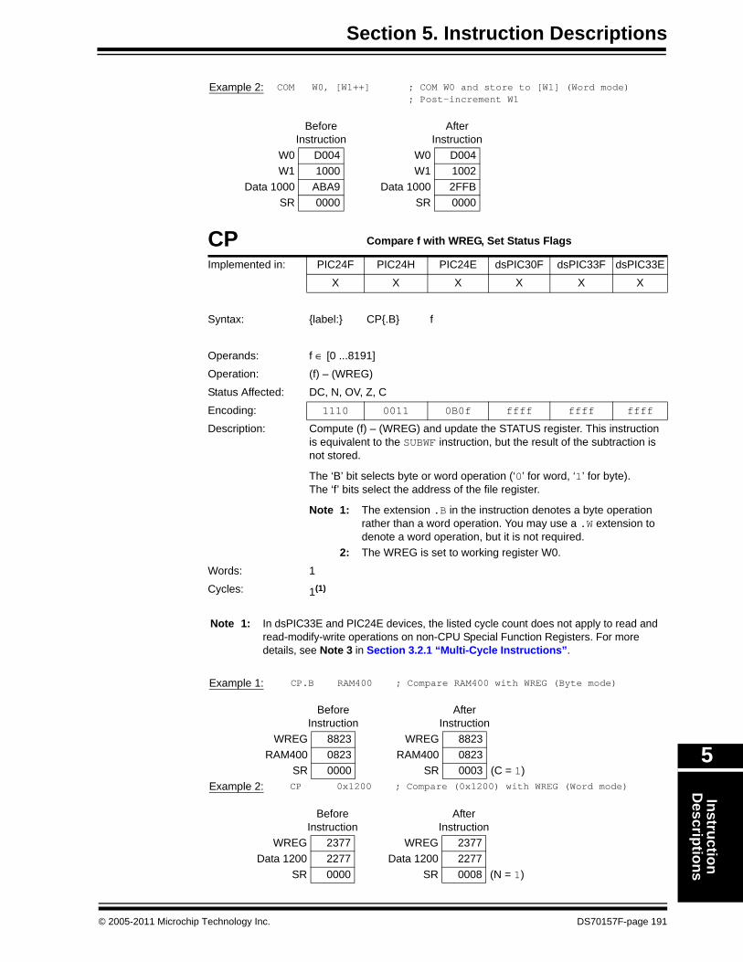
Section 5. Instruction DescriptionsInstruction
Descriptions
5
Example 2: COM W0, [W1++] ; COM W0 and store to [W1] (Word mode); Post-increment W1
Before Instruction
AfterInstruction
W0 D004 W0 D004W1 1000 W1 1002
Data 1000 ABA9 Data 1000 2FFB SR 0000 SR 0000
CP Compare f with WREG, Set Status Flags
Implemented in: PIC24F PIC24H PIC24E dsPIC30F dsPIC33F dsPIC33E
X X X X X X
Syntax: {label:} CP{.B} f
Operands: f ∈ [0 ...8191]
Operation: (f) – (WREG)
Status Affected: DC, N, OV, Z, C
Encoding: 1110 0011 0B0f ffff ffff ffff
Description: Compute (f) – (WREG) and update the STATUS register. This instruction is equivalent to the SUBWF instruction, but the result of the subtraction is not stored.
The ‘B’ bit selects byte or word operation (‘0’ for word, ‘1’ for byte).The ‘f’ bits select the address of the file register.
Note 1: The extension .B in the instruction denotes a byte operation rather than a word operation. You may use a .W extension to denote a word operation, but it is not required.
2: The WREG is set to working register W0.
Words: 1
Cycles: 1(1)
Note 1: In dsPIC33E and PIC24E devices, the listed cycle count does not apply to read and read-modify-write operations on non-CPU Special Function Registers. For more details, see Note 3 in Section 3.2.1 “Multi-Cycle Instructions”.
Example 1: CP.B RAM400 ; Compare RAM400 with WREG (Byte mode)
Before Instruction
AfterInstruction
WREG 8823 WREG 8823RAM400 0823 RAM400 0823
SR 0000 SR 0003 (C = 1)Example 2: CP 0x1200 ; Compare (0x1200) with WREG (Word mode)
Before Instruction
AfterInstruction
WREG 2377 WREG 2377Data 1200 2277 Data 1200 2277
SR 0000 SR 0008 (N = 1)
© 2005-2011 Microchip Technology Inc. DS70157F-page 191

16-bit MCU and DSC Programmer’s Reference Manual
CP Compare Wb with lit5, Set Status Flags
Implemented in: PIC24F PIC24H PIC24E dsPIC30F dsPIC33F dsPIC33E
X X X X
Syntax: {label:} CP{.B} Wb, #lit5
Operands: Wb ∈ [W0 ... W15]lit5 ∈ [ 0 ... 31]
Operation: (Wb) – lit5
Status Affected: DC, N, OV, Z, C
Encoding: 1110 0001 0www wB00 011k kkkk
Description: Compute (Wb) – lit5, and update the STATUS register. This instruction is equivalent to the SUB instruction, but the result of the subtraction is not stored. Register direct addressing must be used for Wb.
The ‘w’ bits select the address of the Wb base register.The ‘B’ bit selects byte or word operation (‘0’ for word, ‘1’ for byte).The ‘k’ bits provide the literal operand, a five-bit integer number.
Note: The extension .B in the instruction denotes a byte operation rather than a word operation. You may use a .W extension to denote a word operation, but it is not required.
Words: 1
Cycles: 1
Example 1: CP.B W4, #0x12 ; Compare W4 with 0x12 (Byte mode)
Before Instruction
AfterInstruction
W4 7711 W4 7711SR 0000 SR 0008 (N = 1)
Example 2: CP W4, #0x12 ; Compare W4 with 0x12 (Word mode)
Before Instruction
AfterInstruction
W4 7713 W4 7713SR 0000 SR 0001 (C = 1)
DS70157F-page 192 © 2005-2011 Microchip Technology Inc.

Section 5. Instruction DescriptionsInstruction
Descriptions
5
CP Compare Wb with lit8, Set Status Flags
Implemented in: PIC24F PIC24H PIC24E dsPIC30F dsPIC33F dsPIC33E
X X
Syntax: {label:} CP{.B} Wb, #lit8
Operands: Wb ∈ [W0 ... W15]lit8 ∈ [ 0 ... 255]
Operation: (Wb) – lit8
Status Affected: DC, N, OV, Z, C
Encoding: 1110 0001 0www wBkk k11k kkkk
Description: Compute (Wb) – lit8, and update the STATUS register. This instruction is equivalent to the SUB instruction, but the result of the subtraction is not stored. Register direct addressing must be used for Wb.
The ‘w’ bits select the address of the Wb base register.The ‘B’ bit selects byte or word operation (‘0’ for word, ‘1’ for byte).The ‘k’ bits provide the literal operand, a five-bit integer number.
Note: The extension .B in the instruction denotes a byte operation rather than a word operation. You may use a .W extension to denote a word operation, but it is not required.
Words: 1
Cycles: 1
Example 1: CP.B W4, #0x12 ; Compare W4 with 0x12 (Byte mode)
Before Instruction
AfterInstruction
W4 7711 W4 7711SR 0000 SR 0009 (N, C = 1)
Example 2: CP W4, #0x12 ; Compare W4 with 0x12 (Word mode)
Before Instruction
AfterInstruction
W4 7713 W4 7713SR 0000 SR 0001 (C = 1)
© 2005-2011 Microchip Technology Inc. DS70157F-page 193
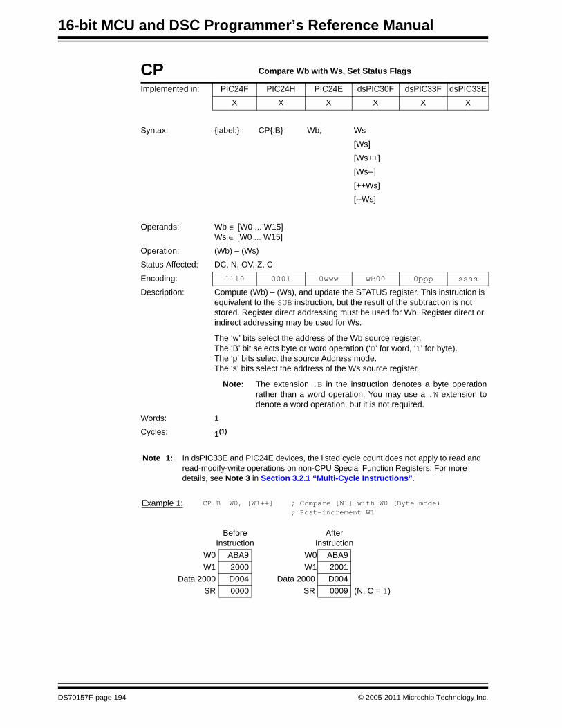
16-bit MCU and DSC Programmer’s Reference Manual
CP Compare Wb with Ws, Set Status Flags
Implemented in: PIC24F PIC24H PIC24E dsPIC30F dsPIC33F dsPIC33E
X X X X X X
Syntax: {label:} CP{.B} Wb, Ws
[Ws]
[Ws++]
[Ws--]
[++Ws]
[--Ws]
Operands: Wb ∈ [W0 ... W15]Ws ∈ [W0 ... W15]
Operation: (Wb) – (Ws)
Status Affected: DC, N, OV, Z, C
Encoding: 1110 0001 0www wB00 0ppp ssss
Description: Compute (Wb) – (Ws), and update the STATUS register. This instruction is equivalent to the SUB instruction, but the result of the subtraction is not stored. Register direct addressing must be used for Wb. Register direct or indirect addressing may be used for Ws.
The ‘w’ bits select the address of the Wb source register.The ‘B’ bit selects byte or word operation (‘0’ for word, ‘1’ for byte).The ‘p’ bits select the source Address mode.The ‘s’ bits select the address of the Ws source register.
Note: The extension .B in the instruction denotes a byte operation rather than a word operation. You may use a .W extension to denote a word operation, but it is not required.
Words: 1
Cycles: 1(1)
Note 1: In dsPIC33E and PIC24E devices, the listed cycle count does not apply to read and read-modify-write operations on non-CPU Special Function Registers. For more details, see Note 3 in Section 3.2.1 “Multi-Cycle Instructions”.
Example 1: CP.B W0, [W1++] ; Compare [W1] with W0 (Byte mode) ; Post-increment W1
Before Instruction
AfterInstruction
W0 ABA9 W0 ABA9W1 2000 W1 2001
Data 2000 D004 Data 2000 D004 SR 0000 SR 0009 (N, C = 1)
DS70157F-page 194 © 2005-2011 Microchip Technology Inc.

Section 5. Instruction DescriptionsInstruction
Descriptions
5
Example 2: CP W5, W6 ; Compare W6 with W5 (Word mode)
Before Instruction
AfterInstruction
W5 2334 W5 2334W6 8001 W6 8001SR 0000 SR 000C (N, OV = 1)
© 2005-2011 Microchip Technology Inc. DS70157F-page 195

16-bit MCU and DSC Programmer’s Reference Manual
CP0 Compare f with 0x0, Set Status Flags
Implemented in: PIC24F PIC24H PIC24E dsPIC30F dsPIC33F dsPIC33E
X X X X X X
Syntax: {label:} CP0{.B} f
Operands: f ∈ [0 ... 8191]
Operation: (f) – 0x0
Status Affected: DC, N, OV, Z, C
Encoding: 1110 0010 0B0f ffff ffff ffff
Description: Compute (f) – 0x0 and update the STATUS register. The result of the subtraction is not stored.
The ‘B’ bit selects byte or word operation (‘0’ for word, ‘1’ for byte). The ‘f’ bits select the address of the file register.
Note: The extension .B in the instruction denotes a byte operation rather than a word operation. You may use a .W extension to denote a word operation, but it is not required.
Words: 1
Cycles: 1(1)
Note 1: In dsPIC33E and PIC24E devices, the listed cycle count does not apply to read and read-modify-write operations on non-CPU Special Function Registers. For more details, see Note 3 in Section 3.2.1 “Multi-Cycle Instructions”.
Example 1: CP0.B RAM100 ; Compare RAM100 with 0x0 (Byte mode)
Before Instruction
AfterInstruction
RAM100 44C3 RAM100 44C3SR 0000 SR 0009 (N, C = 1)
Example 2: CP0 0x1FFE ; Compare (0x1FFE) with 0x0 (Word mode)
Before Instruction
AfterInstruction
Data 1FFE 0001 Data 1FFE 0001SR 0000 SR 0001 (C = 1)
DS70157F-page 196 © 2005-2011 Microchip Technology Inc.

Section 5. Instruction DescriptionsInstruction
Descriptions
5
CP0 Compare Ws with 0x0, Set Status Flags
Implemented in: PIC24F PIC24H PIC24E dsPIC30F dsPIC33F dsPIC33E
X X X X X X
Syntax: {label:} CP0{.B} Ws
[Ws]
[Ws++]
[Ws--]
[++Ws]
[--Ws]
Operands: Ws ∈ [W0 ... W15]
Operation: (Ws) – 0x0000
Status Affected: DC, N, OV, Z, C
Encoding: 1110 0000 0000 0B00 0ppp ssss
Description: Compute (Ws) – 0x0000 and update the STATUS register. The result of the subtraction is not stored. Register direct or indirect addressing may be used for Ws.
The ‘B’ bit selects byte or word operation (‘0’ for word, ‘1’ for byte).The ‘p’ bits select the source Address mode.The ‘s’ bits select the address of the Ws source register.
Note: The extension .B in the instruction denotes a byte operation rather than a word operation. You may use a .W extension to denote a word operation, but it is not required.
Words: 1
Cycles: 1(1)
Note 1: In dsPIC33E and PIC24E devices, the listed cycle count does not apply to read and read-modify-write operations on non-CPU Special Function Registers. For more details, see Note 3 in Section 3.2.1 “Multi-Cycle Instructions”.
Example 1: CP0.B [W4--] ; Compare [W4] with 0 (Byte mode) ; Post-decrement W4
Before Instruction
AfterInstruction
W4 1001 W4 1000Data 1000 0034 Data 1000 0034
SR 0000 SR 0001 (C = 1)
Example 2: CP0 [--W5] ; Compare [--W5] with 0 (Word mode)
Before Instruction
AfterInstruction
W5 2400 W5 23FEData 23FE 9000 Data 23FE 9000
SR 0000 SR 0009 (N, C = 1)
© 2005-2011 Microchip Technology Inc. DS70157F-page 197

16-bit MCU and DSC Programmer’s Reference Manual
CPB Compare f with WREG using Borrow, Set Status Flags
Implemented in: PIC24F PIC24H PIC24E dsPIC30F dsPIC33F dsPIC33E
X X X X X X
Syntax: {label:} CPB{.B} f
Operands: f ∈ [0 ...8191]
Operation: (f) – (WREG) – (C)
Status Affected: DC, N, OV, Z, C
Encoding: 1110 0011 1B0f ffff ffff ffff
Description: Compute (f) – (WREG) – (C), and update the STATUS register. This instruction is equivalent to the SUBB instruction, but the result of the subtraction is not stored.
The ‘B’ bit selects byte or word operation (‘0’ for word, ‘1’ for byte).The ‘f’ bits select the address of the file register.
Note 1: The extension .B in the instruction denotes a byte operation rather than a word operation. You may use a .W extension to denote a word operation, but it is not required.
2: The WREG is set to working register W0. 3: The Z flag is “sticky” for ADDC, CPB, SUBB and SUBBR.
These instructions can only clear Z.
Words: 1
Cycles: 1(1)
Note 1: In dsPIC33E and PIC24E devices, the listed cycle count does not apply to read and read-modify-write operations on non-CPU Special Function Registers. For more details, see Note 3 in Section 3.2.1 “Multi-Cycle Instructions”.
Example 1: CPB.B RAM400 ; Compare RAM400 with WREG using C (Byte mode)
Before Instruction
AfterInstruction
WREG 8823 WREG 8823RAM400 0823 RAM400 0823
SR 0000 SR 0008 (N = 1)
Example 2: CPB 0x1200 ; Compare (0x1200) with WREG using C (Word mode)
Before Instruction
AfterInstruction
WREG 2377 WREG 2377Data 1200 2377 Data 1200 2377
SR 0001 (C = 1) SR 0001 (C = 1)
DS70157F-page 198 © 2005-2011 Microchip Technology Inc.
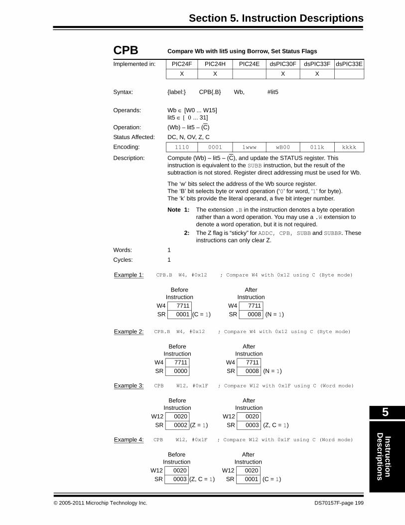
Section 5. Instruction DescriptionsInstruction
Descriptions
5
CPB Compare Wb with lit5 using Borrow, Set Status Flags
Implemented in: PIC24F PIC24H PIC24E dsPIC30F dsPIC33F dsPIC33EX X X X
Syntax: {label:} CPB{.B} Wb, #lit5
Operands: Wb ∈ [W0 ... W15]lit5 ∈ [ 0 ... 31]
Operation: (Wb) – lit5 – (C)Status Affected: DC, N, OV, Z, CEncoding: 1110 0001 1www wB00 011k kkkk
Description: Compute (Wb) – lit5 – (C), and update the STATUS register. This instruction is equivalent to the SUBB instruction, but the result of the subtraction is not stored. Register direct addressing must be used for Wb.
The ‘w’ bits select the address of the Wb source register.The ‘B’ bit selects byte or word operation (‘0’ for word, ‘1’ for byte).The ‘k’ bits provide the literal operand, a five bit integer number.
Note 1: The extension .B in the instruction denotes a byte operation rather than a word operation. You may use a .W extension to denote a word operation, but it is not required.
2: The Z flag is “sticky” for ADDC, CPB, SUBB and SUBBR. These instructions can only clear Z.
Words: 1Cycles: 1
Example 1: CPB.B W4, #0x12 ; Compare W4 with 0x12 using C (Byte mode)
Before Instruction
AfterInstruction
W4 7711 W4 7711SR 0001 (C = 1) SR 0008 (N = 1)
Example 2: CPB.B W4, #0x12 ; Compare W4 with 0x12 using C (Byte mode)
Before Instruction
AfterInstruction
W4 7711 W4 7711SR 0000 SR 0008 (N = 1)
Example 3: CPB W12, #0x1F ; Compare W12 with 0x1F using C (Word mode)
Before Instruction
AfterInstruction
W12 0020 W12 0020SR 0002 (Z = 1) SR 0003 (Z, C = 1)
Example 4: CPB W12, #0x1F ; Compare W12 with 0x1F using C (Word mode)
Before Instruction
AfterInstruction
W12 0020 W12 0020SR 0003 (Z, C = 1) SR 0001 (C = 1)
© 2005-2011 Microchip Technology Inc. DS70157F-page 199

16-bit MCU and DSC Programmer’s Reference Manual
CPB Compare Wb with lit8 using Borrow, Set Status Flags
Implemented in: PIC24F PIC24H PIC24E dsPIC30F dsPIC33F dsPIC33EX X
Syntax: {label:} CPB{.B} Wb, #lit8
Operands: Wb ∈ [W0 ... W15]lit8 ∈ [ 0 ... 255]
Operation: (Wb) – lit8 – (C)Status Affected: DC, N, OV, Z, CEncoding: 1110 0001 1www wBkk k11k kkkk
Description: Compute (Wb) – lit8 – (C), and update the STATUS register. This instruction is equivalent to the SUBB instruction, but the result of the subtraction is not stored. Register direct addressing must be used for Wb.
The ‘w’ bits select the address of the Wb source register.The ‘B’ bit selects byte or word operation (‘0’ for word, ‘1’ for byte).The ‘k’ bits provide the literal operand, a five bit integer number.
Note 1: The extension .B in the instruction denotes a byte operation rather than a word operation. You may use a .W extension to denote a word operation, but it is not required.
2: The Z flag is “sticky” for ADDC, CPB, SUBB and SUBBR. These instructions can only clear Z.
Words: 1Cycles: 1
Example 1: CPB.B W4, #0x12 ; Compare W4 with 0x12 using C (Byte mode)
Before Instruction
AfterInstruction
W4 7711 W4 7711SR 0001 (C = 1) SR 0008 (N = 1)
Example 2: CPB.B W4, #0x12 ; Compare W4 with 0x12 using C (Byte mode)
Before Instruction
AfterInstruction
W4 7711 W4 7711SR 0000 SR 0008 (N = 1)
Example 3: CPB W12, #0x1F ; Compare W12 with 0x1F using C (Word mode)
Before Instruction
AfterInstruction
W12 0020 W12 0020SR 0002 (Z = 1) SR 0003 (Z, C = 1)
Example 4: CPB W12, #0x1F ; Compare W12 with 0x1F using C (Word mode)
Before Instruction
AfterInstruction
W12 0020 W12 0020SR 0003 (Z, C = 1) SR 0001 (C = 1)
DS70157F-page 200 © 2005-2011 Microchip Technology Inc.

Section 5. Instruction DescriptionsInstruction
Descriptions
5
CPB Compare Ws with Wb using Borrow, Set Status Flags
Implemented in: PIC24F PIC24H PIC24E dsPIC30F dsPIC33F dsPIC33E
X X X X X X
Syntax: {label:} CPB{.B} Wb, Ws
[Ws]
[Ws++]
[Ws--]
[++Ws]
[--Ws]
Operands: Wb ∈ [W0 ... W15]Ws ∈ [W0 ... W15]
Operation: (Wb) – (Ws) – (C)
Status Affected: DC, N, OV, Z, C
Encoding: 1110 0001 1www wB00 0ppp ssss
Description: Compute (Wb) – (Ws) – (C), and update the STATUS register. This instruction is equivalent to the SUBB instruction, but the result of the subtraction is not stored. Register direct addressing must be used for Wb. Register direct or indirect addressing may be used for Ws.
The ‘w’ bits select the address of the Wb source register.The ‘B’ bit selects byte or word operation (‘0’ for word, ‘1’ for byte).The ‘p’ bits select the source Address mode.The ‘s’ bits select the address of the Ws source register.
Note 1: The extension .B in the instruction denotes a byte operation rather than a word operation. You may use a .W extension to denote a word operation, but it is not required.
2: The Z flag is “sticky” for ADDC, CPB, SUBB and SUBBR. These instructions can only clear Z.
Words: 1
Cycles: 1(1)
Note 1: In dsPIC33E and PIC24E devices, the listed cycle count does not apply to read and read-modify-write operations on non-CPU Special Function Registers. For more details, see Note 3 in Section 3.2.1 “Multi-Cycle Instructions”.
Example 1: CPB.B W0, [W1++] ; Compare [W1] with W0 using C (Byte mode); Post-increment W1
Before Instruction
AfterInstruction
W0 ABA9 W0 ABA9W1 1000 W1 1001
Data 1000 D0A9 Data 1000 D0A9 SR 0002 (Z = 1) SR 0008 (N = 1)
© 2005-2011 Microchip Technology Inc. DS70157F-page 201

16-bit MCU and DSC Programmer’s Reference Manual
Example 2: CPB.B W0, [W1++] ; Compare [W1] with W0 using C (Byte mode); Post-increment W1
Before Instruction
AfterInstruction
W0 ABA9 W0 ABA9W1 1000 W1 1001
Data 1000 D0A9 Data 1000 D0A9 SR 0001 (C = 1) SR 0001 (C = 1)
Example 3: CPB W4, W5 ; Compare W5 with W4 using C (Word mode)
Before Instruction
AfterInstruction
W4 4000 W4 4000W5 3000 W5 3000SR 0001 (C = 1) SR 0001 (C = 1)
DS70157F-page 202 © 2005-2011 Microchip Technology Inc.

Section 5. Instruction DescriptionsInstruction
Descriptions
5
CPBEQ Compare Wb with Wn, Branch if Equal (Wb = Wn)
Implemented in: PIC24F PIC24H PIC24E dsPIC30F dsPIC33F dsPIC33E
X X
Syntax: {label:} CPBEQ{.B} Wb, Wn, Expr
Operands: Wb ∈ [W0 ... W15]Wn ∈ [W0 ... W15]
Operation: (Wb) – (Wn)If (Wb) = (Wn), [(PC+2) + 2 * Expr] → PC and NOP → Instruction Register
Status Affected: None
Encoding: 1110 0111 1www wBnn nnnn ssss
Description: Compare the contents of Wb with the contents of Wn by performing the subtraction (Wb) – (Wn), but do not store the result. If (Wb) = (Wn), the next instruction (fetched during the current instruction execution) is discarded, the PC is recalculated based on the 6-bit signed offset specified by Expr, and on the next cycle, a NOP is executed instead. If (Wb) ≠ (Wn), the next instruction is executed as normal (branch is not taken).
The ‘w’ bits select the address of the Wb source register.The ‘B’ bit selects byte or word operation (‘0’ for word, ‘1’ for byte).The ‘s’ bits select the address of the Wn source register.The ‘n’ bits select the offset of the branch destination.
Note: The extension .B in the instruction denotes a byte operation rather than a word operation. You may use a .W extension to denote a word operation, but it is not required.
Words: 1
Cycles: 1 (5 if branch taken)
Example 1: 002000 HERE:CPBEQ.B W0, W1, BYPASS; If W0 = W1 (Byte mode),002002 ADD W2, W3, W4; Perform branch to BYPASS002004 . . .002006 . . .002008 BYPASS: . . .00200A . . .
Before Instruction
After Instruction
PC 00 2000 PC 00 2008W0 1000 W0 1000W1 1000 W1 1000SR 0000 SR 0002 (z = 1)
© 2005-2011 Microchip Technology Inc. DS70157F-page 203

16-bit MCU and DSC Programmer’s Reference Manual
CPBGT Signed Compare Wb with Wn, Branch if Greater Than (Wb > Wn)
Implemented in: PIC24F PIC24H PIC24E dsPIC30F dsPIC33F dsPIC33E
X X
Syntax: {label:} CPBGT{.B} Wb, Wn, Expr
Operands: Wb ∈ [W0 ... W15]Wn ∈ [W0 ... W15]
Operation: (Wb) – (Wn)If (Wb) = (Wn), [(PC+2) + 2 * Expr] → PC and NOP → Instruction Register
Status Affected: None
Encoding: 1110 0110 0www wBnn nnnn ssss
Description: Compare the contents of Wb with the contents of Wn by performing the subtraction (Wb) – (Wn), but do not store the result. If (Wb) = (Wn), the next instruction (fetched during the current instruction execution) is discarded, the PC is recalculated based on the 6-bit signed offset specified by Expr, and on the next cycle, a NOP is executed instead. If (Wb) ≠ (Wn), the next instruction is executed as normal (branch is not taken).
The ‘w’ bits select the address of the Wb source register.The ‘B’ bit selects byte or word operation (‘0’ for word, ‘1’ for byte).The ‘s’ bits select the address of the Wn source register.The ‘n’ bits select the offset of the branch destination.
Note: The extension .B in the instruction denotes a byte operation rather than a word operation. You may use a .W extension to denote a word operation, but it is not required.
Words: 1
Cycles: 1 (5 if branch taken)
Example 1: 002000 HERE: CPBGT.B W0, W1, BYPASS ; If W0 > W1 (Byte mode),002002 ADD W2, W3, W4 ; Perform branch to BYPASS002004 . . .002006 . . .002008 BYPASS . . .00200A . . .
Before Instruction
After Instruction
PC 00 2000 PC 00 2008W0 30FF W0 00FFW1 26FE W1 26FESR 0000 SR 0000 (N, C = 0)
DS70157F-page 204 © 2005-2011 Microchip Technology Inc.
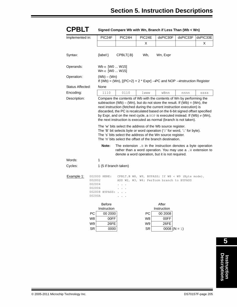
Section 5. Instruction DescriptionsInstruction
Descriptions
5
CPBLT Signed Compare Wb with Wn, Branch if Less Than (Wb < Wn)
Implemented in: PIC24F PIC24H PIC24E dsPIC30F dsPIC33F dsPIC33E
X X
Syntax: {label:} CPBLT{.B} Wb, Wn, Expr
Operands: Wb ∈ [W0 ... W15]Wn ∈ [W0 ... W15]
Operation: (Wb) – (Wn)If (Wb) = (Wn), [(PC+2) + 2 * Expr] → PC and NOP → Instruction Register
Status Affected: None
Encoding: 1110 0110 1www wBnn nnnn ssss
Description: Compare the contents of Wb with the contents of Wn by performing the subtraction (Wb) – (Wn), but do not store the result. If (Wb) = (Wn), the next instruction (fetched during the current instruction execution) is discarded, the PC is recalculated based on the 6-bit signed offset specified by Expr, and on the next cycle, a NOP is executed instead. If (Wb) ≠ (Wn), the next instruction is executed as normal (branch is not taken).
The ‘w’ bits select the address of the Wb source register.The ‘B’ bit selects byte or word operation (‘0’ for word, ‘1’ for byte).The ‘s’ bits select the address of the Wn source register.The ‘n’ bits select the offset of the branch destination.
Note: The extension .B in the instruction denotes a byte operation rather than a word operation. You may use a .W extension to denote a word operation, but it is not required.
Words: 1
Cycles: 1 (5 if branch taken)
Example 1: 002000 HERE: CPBLT.B W8, W9, BYPASS; If W8 < W9 (Byte mode),002002 ADD W2, W3, W4; Perform branch to BYPASS002004 . . .002006 . . .002008 BYPASS: . . .00200A . . .
Before Instruction
After Instruction
PC 00 2000 PC 00 2008W8 00FF W8 00FFW9 26FE W9 26FESR 0000 SR 0008 (N = 1)
© 2005-2011 Microchip Technology Inc. DS70157F-page 205

16-bit MCU and DSC Programmer’s Reference Manual
CPBNE Compare Wb with Wn, Branch if Not Equal (Wb ≠ Wn)
Implemented in: PIC24F PIC24H PIC24E dsPIC30F dsPIC33F dsPIC33E
X X
Syntax: {label:} CPBNE{.B} Wb, Wn, Expr
Operands: Wb ∈ [W0 ... W15]Wn ∈ [W0 ... W15]
Operation: (Wb) – (Wn)If (Wb) = (Wn), [(PC+2) + 2 * Expr] → PC and NOP → Instruction Register
Status Affected: None
Encoding: 1110 0111 0www wBnn nnnn ssss
Description: Compare the contents of Wb with the contents of Wn by performing the subtraction (Wb) – (Wn), but do not store the result. If (Wb) = (Wn), the next instruction (fetched during the current instruction execution) is discarded, the PC is recalculated based on the 6-bit signed offset specified by Expr, and on the next cycle, a NOP is executed instead. If (Wb) ≠ (Wn), the next instruction is executed as normal (branch is not taken).
The ‘w’ bits select the address of the Wb source register.The ‘B’ bit selects byte or word operation (‘0’ for word, ‘1’ for byte).The ‘s’ bits select the address of the Wn source register.The ‘n’ bits select the offset of the branch destination.
Note: The extension .B in the instruction denotes a byte operation rather than a word operation. You may use a .W extension to denote a word operation, but it is not required.
Words: 1
Cycles: 1 (5 if branch taken)
Example 1: 002000 HERE: CPBNE.B W2, W3, BYPASS ; If W2 != W3 (Byte mode),002002 ADD W2, W3, W4 ; Perform branch to BYPASS002004 . . .002006 . . .002008 BYPASS: . . .00200A . . .
Before Instruction
After Instruction
PC 00 2000 PC 00 200AW2 00FF W2 00FFW3 26FE W3 26FESR 0000 SR 0001 (C = 1)
DS70157F-page 206 © 2005-2011 Microchip Technology Inc.

Section 5. Instruction DescriptionsInstruction
Descriptions
5
CPSEQ Compare Wb with Wn, Skip if Equal (Wb = Wn)
Implemented in: PIC24F PIC24H PIC24E dsPIC30F dsPIC33F dsPIC33E
X X X X
Syntax: {label:} CPSEQ{.B} Wb, Wn
Operands: Wb ∈ [W0 ... W15]Wn ∈ [W0 ... W15]
Operation: (Wb) – (Wn)Skip if (Wb) = (Wn)
Status Affected: None
Encoding: 1110 0111 1www wB00 0000 ssss
Description: Compare the contents of Wb with the contents of Wn by performing the subtraction (Wb) – (Wn), but do not store the result. If (Wb) = (Wn), the next instruction (fetched during the current instruction execution) is discarded and on the next cycle, a NOP is executed instead. If (Wb) ≠ (Wn), the next instruction is executed as normal.
The ‘w’ bits select the address of the Wb source register.The ‘B’ bit selects byte or word operation (‘0’ for word, ‘1’ for byte).The ‘s’ bits select the address of the Wn source register.
Note: The extension .B in the instruction denotes a byte operation rather than a word operation. You may use a .W extension to denote a word operation, but it is not required.
Words: 1
Cycles: 1 (2 or 3 if skip taken)
Example 1: 002000 HERE:CPSEQ.BW0, W1; If W0 = W1 (Byte mode),002002GOTOBYPASS; skip the GOTO002004 . . .002006 . . .002008 BYPASS: . . .00200A . . .
Before Instruction
After Instruction
PC 00 2000 PC 00 2002W0 1001 W0 1001W1 1000 W1 1000SR 0000 SR 0000
Example 2: 018000 HERE: CPSEQ W4, W8; If W4 = W8 (Word mode),018002 CALL _FIR; skip the subroutine call018006 ...018008 ...
Before Instruction
After Instruction
PC 01 8000 PC 01 8006W4 3344 W4 3344W8 3344 W8 3344SR 0002 (Z = 1) SR 0002 (Z = 1)
© 2005-2011 Microchip Technology Inc. DS70157F-page 207

16-bit MCU and DSC Programmer’s Reference Manual
CPSEQ Compare Wb with Wn, Skip if Equal (Wb = Wn)
Implemented in: PIC24F PIC24H PIC24E dsPIC30F dsPIC33F dsPIC33E
X X
Syntax: {label:} CPSEQ{.B} Wb, Wn
Operands: Wb ∈ [W0 ... W15]Wn ∈ [W0 ... W15]
Operation: (Wb) – (Wn)Skip if (Wb) = (Wn)
Status Affected: None
Encoding: 1110 0111 1www wB00 0001 ssss
Description: Compare the contents of Wb with the contents of Wn by performing the subtraction (Wb) – (Wn), but do not store the result. If (Wb) = (Wn), the next instruction (fetched during the current instruction execution) is discarded and on the next cycle, a NOP is executed instead. If (Wb) ≠ (Wn), the next instruction is executed as normal.
The ‘w’ bits select the address of the Wb source register.The ‘B’ bit selects byte or word operation (‘0’ for word, ‘1’ for byte).The ‘s’ bits select the address of the Wn source register.
Note: The extension .B in the instruction denotes a byte operation rather than a word operation. You may use a .W extension to denote a word operation, but it is not required.
Words: 1
Cycles: 1 (2 or 3 if skip taken)
Example 1: 002000 HERE:CPSEQ.BW0, W1; If W0 = W1 (Byte mode),002002GOTOBYPASS; skip the GOTO002004 . . .002006 . . .002008 BYPASS: . . .00200A . . .
Before Instruction
After Instruction
PC 00 2000 PC 00 2002W0 1001 W0 1001W1 1000 W1 1000SR 0000 SR 0000
DS70157F-page 208 © 2005-2011 Microchip Technology Inc.

Section 5. Instruction DescriptionsInstruction
Descriptions
5
Example 2: 018000 HERE: CPSEQ W4, W8; If W4 = W8 (Word mode),018002 CALL _FIR; skip the subroutine call018006 ...018008 ...
Before Instruction
After Instruction
PC 01 8000 PC 01 8006W4 3344 W4 3344W8 3344 W8 3344SR 0002 (Z = 1) SR 0002 (Z = 1)
© 2005-2011 Microchip Technology Inc. DS70157F-page 209

16-bit MCU and DSC Programmer’s Reference Manual
CPSGT Signed Compare Wb with Wn, Skip if Greater Than (Wb > Wn)
Implemented in: PIC24F PIC24H PIC24E dsPIC30F dsPIC33F dsPIC33E
X X X X
Syntax: {label:} CPSGT{.B} Wb, Wn
Operands: Wb ∈ [W0 ... W15]Wn ∈ [W0 ... W15]
Operation: (Wb) – (Wn)Skip if (Wb) > (Wn)
Status Affected: None
Encoding: 1110 0110 0www wB00 0000 ssss
Description: Compare the contents of Wb with the contents of Wn by performing the subtraction (Wb) – (Wn), but do not store the result. If (Wb) > (Wn), the next instruction (fetched during the current instruction execution) is discarded and on the next cycle, a NOP is executed instead. Otherwise, the next instruction is executed as normal.
The ‘w’ bits select the address of the Wb source register.The ‘B’ bit selects byte or word operation (‘0’ for word, ‘1’ for byte).The ‘s’ bits select the address of the Wn source register.
Note: The extension .B in the instruction denotes a byte operation rather than a word operation. You may use a .W extension to denote a word operation, but it is not required.
Words: 1
Cycles: 1 (2 or 3 if skip taken)
Example 1: 002000 HERE: CPSGT.B W0, W1; If W0 > W1 (Byte mode),002002 GOTO BYPASS; skip the GOTO002006 . . .002008 . . .00200A BYPASS . . .00200C . . .
Before Instruction
After Instruction
PC 00 2000 PC 00 2006W0 00FF W0 00FFW1 26FE W1 26FESR 0009 (N, C = 1) SR 0009 (N, C = 1)
Example 2: 018000 HERE: CPSGT W4, W5; If W4 > W5 (Word mode),018002 CALL _FIR; skip the subroutine call018006 ...018008 ...
Before Instruction
After Instruction
PC 01 8000 PC 01 8002W4 2600 W4 2600W5 2600 W5 2600SR 0004 (OV = 1) SR 0004 (OV = 1)
DS70157F-page 210 © 2005-2011 Microchip Technology Inc.

Section 5. Instruction DescriptionsInstruction
Descriptions
5
CPSGT Signed Compare Wb with Wn, Skip if Greater Than (Wb > Wn)
Implemented in: PIC24F PIC24H PIC24E dsPIC30F dsPIC33F dsPIC33E
X X
Syntax: {label:} CPSGT{.B} Wb, Wn
Operands: Wb ∈ [W0 ... W15]Wn ∈ [W0 ... W15]
Operation: (Wb) – (Wn)Skip if (Wb) > (Wn)
Status Affected: None
Encoding: 1110 0110 0www wB00 0001 ssss
Description: Compare the contents of Wb with the contents of Wn by performing the subtraction (Wb) – (Wn), but do not store the result. If (Wb) > (Wn), the next instruction (fetched during the current instruction execution) is discarded and on the next cycle, a NOP is executed instead. Otherwise, the next instruction is executed as normal.
The ‘w’ bits select the address of the Wb source register.The ‘B’ bit selects byte or word operation (‘0’ for word, ‘1’ for byte).The ‘s’ bits select the address of the Wn source register.
Note: The extension .B in the instruction denotes a byte operation rather than a word operation. You may use a .W extension to denote a word operation, but it is not required.
Words: 1
Cycles: 1 (2 or 3 if skip taken)
Example 1: 002000 HERE: CPSGT.B W0, W1; If W0 > W1 (Byte mode),002002 GOTO BYPASS; skip the GOTO002006 . . .002008 . . .00200A BYPASS . . .00200C . . .
Before Instruction
After Instruction
PC 00 2000 PC 00 2006W0 00FF W0 00FFW1 26FE W1 26FESR 0009 (N, C = 1) SR 0009 (N, C = 1)
Example 2: 018000 HERE: CPSGT W4, W5; If W4 > W5 (Word mode),018002 CALL _FIR; skip the subroutine call018006 ...018008 ...
Before Instruction
After Instruction
PC 01 8000 PC 01 8002W4 2600 W4 2600W5 2600 W5 2600SR 0004 (OV = 1) SR 0004 (OV = 1)
© 2005-2011 Microchip Technology Inc. DS70157F-page 211

16-bit MCU and DSC Programmer’s Reference Manual
CPSLT Signed Compare Wb with Wn, Skip if Less Than (Wb < Wn)
Implemented in: PIC24F PIC24H PIC24E dsPIC30F dsPIC33F dsPIC33E
X X X X
Syntax: {label:} CPSLT{.B} Wb, Wn
Operands: Wb ∈ [W0 ... W15]Wn ∈ [W0 ... W15]
Operation: (Wb) – (Wn)Skip if (Wb) < (Wn)
Status Affected: None
Encoding: 1110 0110 1www wB00 0000 ssss
Description: Compare the contents of Wb with the contents of Wn by performing the subtraction (Wb) – (Wn), but do not store the result. If (Wb) < (Wn), the next instruction (fetched during the current instruction execution) is discarded and on the next cycle, a NOP is executed instead. Otherwise, the next instruction is executed as normal.
The ‘w’ bits select the address of the Wb source register.The ‘B’ bit selects byte or word operation (‘0’ for word, ‘1’ for byte).The ‘s’ bits select the address of the Wn source register.
Note: The extension .B in the instruction denotes a byte operation rather than a word operation. You may use a .W extension to denote a word operation, but it is not required.
Words: 1
Cycles: 1 (2 or 3 if skip taken)
Example 1: 002000 HERE: CPSLT.B W8, W9; If W8 < W9 (Byte mode),002002 GOTO BYPASS; skip the GOTO002006 . . .002008 . . .00200A BYPASS: . . .00200C . . .
Before Instruction
After Instruction
PC 00 2000 PC 00 2002W8 00FF W8 00FFW9 26FE W9 26FESR 0008 (N = 1) SR 0008 (N = 1)
Example 2: 018000 HERE: CPSLT W3, W6; If W3 < W6 (Word mode),018002 CALL _FIR; skip the subroutine call018006 . . .018008 . . .
Before Instruction
After Instruction
PC 01 8000 PC 01 8006W3 2600 W3 2600W6 3000 W6 3000SR 0000 SR 0000
DS70157F-page 212 © 2005-2011 Microchip Technology Inc.

Section 5. Instruction DescriptionsInstruction
Descriptions
5
CPSLT Signed Compare Wb with Wn, Skip if Less Than (Wb < Wn)
Implemented in: PIC24F PIC24H PIC24E dsPIC30F dsPIC33F dsPIC33E
X X
Syntax: {label:} CPSLT{.B} Wb, Wn
Operands: Wb ∈ [W0 ... W15]Wn ∈ [W0 ... W15]
Operation: (Wb) – (Wn)Skip if (Wb) < (Wn)
Status Affected: None
Encoding: 1110 0110 1www wB00 0001 ssss
Description: Compare the contents of Wb with the contents of Wn by performing the subtraction (Wb) – (Wn), but do not store the result. If (Wb) < (Wn), the next instruction (fetched during the current instruction execution) is discarded and on the next cycle, a NOP is executed instead. Otherwise, the next instruction is executed as normal.
The ‘w’ bits select the address of the Wb source register.The ‘B’ bit selects byte or word operation (‘0’ for word, ‘1’ for byte).The ‘s’ bits select the address of the Wn source register.
Note: The extension .B in the instruction denotes a byte operation rather than a word operation. You may use a .W extension to denote a word operation, but it is not required.
Words: 1
Cycles: 1 (2 or 3 if skip taken)
Example 1: 002000 HERE: CPSLT.B W8, W9; If W8 < W9 (Byte mode),002002 GOTO BYPASS; skip the GOTO002006 . . .002008 . . .00200A BYPASS: . . .00200C . . .
Before Instruction
After Instruction
PC 00 2000 PC 00 2002W8 00FF W8 00FFW9 26FE W9 26FESR 0008 (N = 1) SR 0008 (N = 1)
Example 2: 018000 HERE: CPSLT W3, W6; If W3 < W6 (Word mode),018002 CALL _FIR; skip the subroutine call018006 . . .018008 . . .
Before Instruction
After Instruction
PC 01 8000 PC 01 8006W3 2600 W3 2600W6 3000 W6 3000SR 0000 SR 0000
© 2005-2011 Microchip Technology Inc. DS70157F-page 213

16-bit MCU and DSC Programmer’s Reference Manual
CPSNE Signed Compare Wb with Wn, Skip if Not Equal (Wb ≠ Wn)
Implemented in: PIC24F PIC24H PIC24E dsPIC30F dsPIC33F dsPIC33E
X X X X
Syntax: {label:} CPSNE{.B} Wb, Wn
Operands: Wb ∈ [W0 ... W15]Wn ∈ [W0 ... W15]
Operation: (Wb) – (Wn)Skip if (Wb) ≠ (Wn)
Status Affected: None
Encoding: 1110 0111 0www wB00 0000 ssss
Description: Compare the contents of Wb with the contents of Wn by performing the subtraction (Wb) – (Wn), but do not store the result. If (Wb) ≠ (Wn), the next instruction (fetched during the current instruction execution) is discarded and on the next cycle, a NOP is executed instead. Otherwise, the next instruction is executed as normal.
The ‘w’ bits select the address of the Wb source register.The ‘B’ bit selects byte or word operation (‘0’ for word, ‘1’ for byte).The ‘s’ bits select the address of the Wn source register.
Note: The extension .B in the instruction denotes a byte operation rather than a word operation. You may use a .W extension to denote a word operation, but it is not required.
Words: 1
Cycles: 1 (2 or 3 if skip taken)
Example 1: 002000 HERE: CPSNE.B W2, W3 ; If W2 != W3 (Byte mode),002002 GOTO BYPASS ; skip the GOTO002006 . . .002008 . . .00200A BYPASS: . . .00200C . . .
Before Instruction
After Instruction
PC 00 2000 PC 00 2006W2 00FF W2 00FFW3 26FE W3 26FESR 0001 (C = 1) SR 0001 (C = 1)
Example 2: 018000 HERE: CPSNE W0, W8 ; If W0 != W8 (Word mode),018002 CALL _FIR ; skip the subroutine call018006 ...018008 ...
Before Instruction
After Instruction
PC 01 8000 PC 01 8002W0 3000 W0 3000W8 3000 W8 3000SR 0000 SR 0000
DS70157F-page 214 © 2005-2011 Microchip Technology Inc.

Section 5. Instruction DescriptionsInstruction
Descriptions
5
CPSNE Signed Compare Wb with Wn, Skip if Not Equal (Wb ≠ Wn)
Implemented in: PIC24F PIC24H PIC24E dsPIC30F dsPIC33F dsPIC33E
X X
Syntax: {label:} CPSNE{.B} Wb, Wn
Operands: Wb ∈ [W0 ... W15]Wn ∈ [W0 ... W15]
Operation: (Wb) – (Wn)Skip if (Wb) ≠ (Wn)
Status Affected: None
Encoding: 1110 0111 0www wB00 0001 ssss
Description: Compare the contents of Wb with the contents of Wn by performing the subtraction (Wb) – (Wn), but do not store the result. If (Wb) ≠ (Wn), the next instruction (fetched during the current instruction execution) is discarded and on the next cycle, a NOP is executed instead. Otherwise, the next instruction is executed as normal.
The ‘w’ bits select the address of the Wb source register.The ‘B’ bit selects byte or word operation (‘0’ for word, ‘1’ for byte).The ‘s’ bits select the address of the Wn source register.
Note: The extension .B in the instruction denotes a byte operation rather than a word operation. You may use a .W extension to denote a word operation, but it is not required.
Words: 1
Cycles: 1 (2 or 3 if skip taken)
Example 1: 002000 HERE: CPSNE.B W2, W3 ; If W2 != W3 (Byte mode),002002 GOTO BYPASS ; skip the GOTO002006 . . .002008 . . .00200A BYPASS: . . .00200C . . .
Before Instruction
After Instruction
PC 00 2000 PC 00 2006W2 00FF W2 00FFW3 26FE W3 26FESR 0001 (C = 1) SR 0001 (C = 1)
Example 2: 018000 HERE: CPSNE W0, W8 ; If W0 != W8 (Word mode),018002 CALL _FIR ; skip the subroutine call018006 ...018008 ...
Before Instruction
After Instruction
PC 01 8000 PC 01 8002W0 3000 W0 3000W8 3000 W8 3000SR 0000 SR 0000
© 2005-2011 Microchip Technology Inc. DS70157F-page 215

16-bit MCU and DSC Programmer’s Reference Manual
DAW.B Decimal Adjust Wn
Implemented in: PIC24F PIC24H PIC24E dsPIC30F dsPIC33F dsPIC33E
X X X X X X
Syntax: {label:} DAW.B Wn
Operands: Wn ∈ [W0 ... W15]
Operation: If (Wn<3:0> > 9) or (DC = 1) (Wn<3:0>) + 6 → Wn<3:0>Else (Wn<3:0>) → Wn<3:0>
If (Wn<7:4> > 9) or (C = 1) (Wn<7:4>) + 6 → Wn<7:4>Else (Wn<7:4>) → Wn<7:4>
Status Affected: C
Encoding: 1111 1101 0100 0000 0000 ssss
Description: Adjust the Least Significant Byte in Wn to produce a binary coded decimal (BCD) result. The Most Significant Byte of Wn is not changed, and the Carry flag is used to indicate any decimal rollover. Register direct addressing must be used for Wn.
The ‘s’ bits select the source/destination register.
Note 1: This instruction is used to correct the data format after two packed BCD bytes have been added.
2: This instruction operates in Byte mode only and the .B extension must be included with the opcode.
Words: 1
Cycles: 1
Example 1: DAW.B W0 ; Decimal adjust W0
Before Instruction
AfterInstruction
W0 771A W0 7720SR 0002 (DC = 1) SR 0002 (DC = 1)
Example 2: DAW.B W3 ; Decimal adjust W3
Before Instruction
AfterInstruction
W3 77AA W3 7710SR 0000 SR 0001 (C = 1)
DS70157F-page 216 © 2005-2011 Microchip Technology Inc.
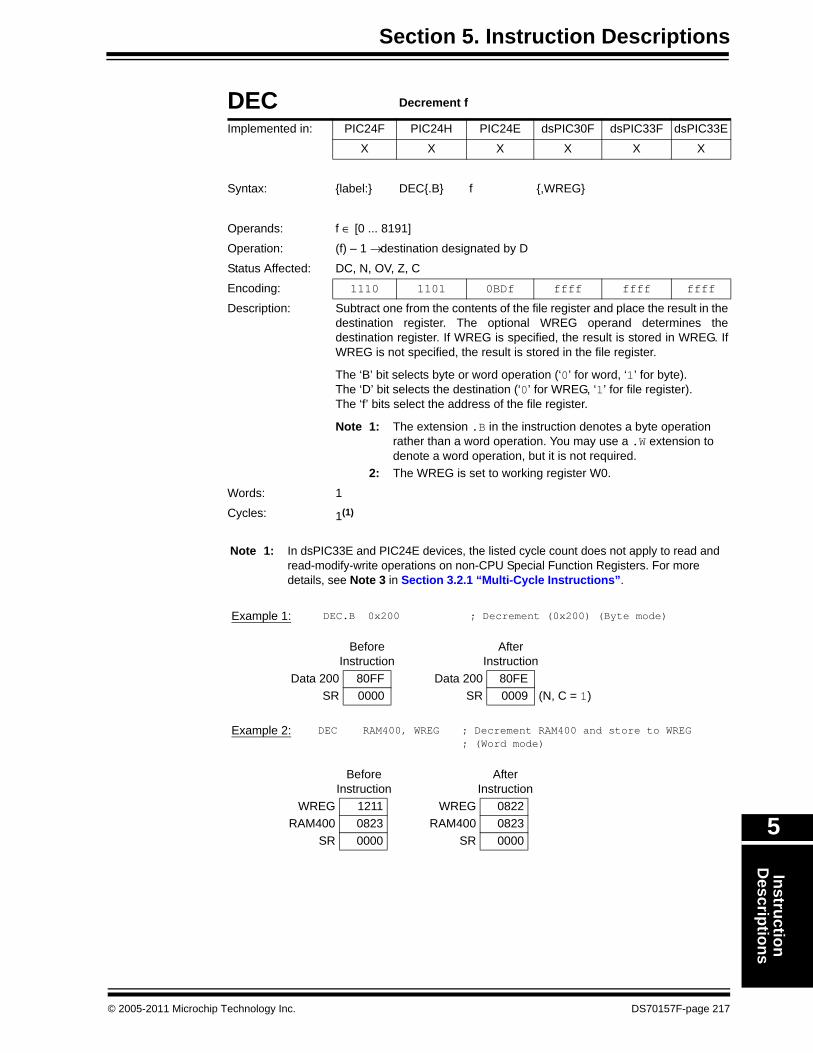
Section 5. Instruction DescriptionsInstruction
Descriptions
5
DEC Decrement f
Implemented in: PIC24F PIC24H PIC24E dsPIC30F dsPIC33F dsPIC33E
X X X X X X
Syntax: {label:} DEC{.B} f {,WREG}
Operands: f ∈ [0 ... 8191]
Operation: (f) – 1 → destination designated by D
Status Affected: DC, N, OV, Z, C
Encoding: 1110 1101 0BDf ffff ffff ffff
Description: Subtract one from the contents of the file register and place the result in the destination register. The optional WREG operand determines the destination register. If WREG is specified, the result is stored in WREG. If WREG is not specified, the result is stored in the file register.
The ‘B’ bit selects byte or word operation (‘0’ for word, ‘1’ for byte).The ‘D’ bit selects the destination (‘0’ for WREG, ‘1’ for file register).The ‘f’ bits select the address of the file register.
Note 1: The extension .B in the instruction denotes a byte operation rather than a word operation. You may use a .W extension to denote a word operation, but it is not required.
2: The WREG is set to working register W0.
Words: 1
Cycles: 1(1)
Note 1: In dsPIC33E and PIC24E devices, the listed cycle count does not apply to read and read-modify-write operations on non-CPU Special Function Registers. For more details, see Note 3 in Section 3.2.1 “Multi-Cycle Instructions”.
Example 1: DEC.B 0x200 ; Decrement (0x200) (Byte mode)
Before Instruction
AfterInstruction
Data 200 80FF Data 200 80FESR 0000 SR 0009 (N, C = 1)
Example 2: DEC RAM400, WREG ; Decrement RAM400 and store to WREG ; (Word mode)
Before Instruction
AfterInstruction
WREG 1211 WREG 0822RAM400 0823 RAM400 0823
SR 0000 SR 0000
© 2005-2011 Microchip Technology Inc. DS70157F-page 217

16-bit MCU and DSC Programmer’s Reference Manual
DEC Decrement Ws
Implemented in: PIC24F PIC24H PIC24E dsPIC30F dsPIC33F dsPIC33E
X X X X X X
Syntax: {label:} DEC{.B} Ws, Wd
[Ws], [Wd]
[Ws++], [Wd++]
[Ws--], [Wd--]
[++Ws], [++Wd]
[--Ws], [--Wd]
Operands: Ws ∈ [W0 ... W15]Wd ∈ [W0 ... W15]
Operation: (Ws) – 1 → Wd
Status Affected: DC, N, OV, Z, C
Encoding: 1110 1001 0Bqq qddd dppp ssss
Description: Subtract one from the contents of the source register Ws and place the result in the destination register Wd. Either register direct or indirect addressing may be used by Ws and Wd.
The ‘B’ bit selects byte or word operation (‘0’ for word, ‘1’ for byte).The ‘q’ bits select the destination Address mode.The ‘d’ bits select the destination register.The ‘p’ bits select the source Address mode.The ‘s’ bits select the source register.
Note: The extension .B in the instruction denotes a byte operation rather than a word operation. You may use a .W extension to denote a word operation, but it is not required.
Words: 1
Cycles: 1(1)
Note 1: In dsPIC33E and PIC24E devices, the listed cycle count does not apply to read and read-modify-write operations on non-CPU Special Function Registers. For more details, see Note 3 in Section 3.2.1 “Multi-Cycle Instructions”.
Example 1: DEC.B [W7++], [W8++] ; DEC [W7] and store to [W8] (Byte mode) ; Post-increment W7, W8
Before Instruction
AfterInstruction
W7 2301 W7 2302W8 2400 W8 2401
Data 2300 5607 Data 2300 5607 Data 2400 ABCD Data 2400 AB55
SR 0000 SR 0000
DS70157F-page 218 © 2005-2011 Microchip Technology Inc.

Section 5. Instruction DescriptionsInstruction
Descriptions
5
Example 2: DEC W5, [W6++] ; Decrement W5 and store to [W6] (Word mode) ; Post-increment W6
Before Instruction
AfterInstruction
W5 D004 W5 D004W6 2000 W6 2002
Data 2000 ABA9 Data 2000 D003 SR 0000 SR 0009 (N, C = 1)
© 2005-2011 Microchip Technology Inc. DS70157F-page 219

16-bit MCU and DSC Programmer’s Reference Manual
DEC2 Decrement f by 2
Implemented in: PIC24F PIC24H PIC24E dsPIC30F dsPIC33F dsPIC33E
X X X X X X
Syntax: {label:} DEC2{.B} f {,WREG}
Operands: f ∈ [0 ... 8191]
Operation: (f) – 2 → destination designated by D
Status Affected: DC, N, OV, Z, C
Encoding: 1110 1101 1BDf ffff ffff ffff
Description: Subtract two from the contents of the file register and place the result in the destination register. The optional WREG operand determines the destination register. If WREG is specified, the result is stored in WREG. If WREG is not specified, the result is stored in the file register.
The ‘B’ bit selects byte or word operation (‘0’ for word, ‘1’ for byte).The ‘D’ bit selects the destination (‘0’ for WREG, ‘1’ for file register).The ‘f’ bits select the address of the file register.
Note: The extension .B in the instruction denotes a byte operation rather than a word operation. You may use a .W extension to denote a word operation, but it is not required.
Words: 1
Cycles: 1(1)
Note 1: In dsPIC33E and PIC24E devices, the listed cycle count does not apply to read and read-modify-write operations on non-CPU Special Function Registers. For more details, see Note 3 in Section 3.2.1 “Multi-Cycle Instructions”.
Example 1: DEC2.B 0x200 ; Decrement (0x200) by 2 (Byte mode)
Before Instruction
AfterInstruction
Data 200 80FF Data 200 80FDSR 0000 SR 0009 (N, C = 1)
Example 2: DEC2 RAM400, WREG ; Decrement RAM400 by 2 and ; store to WREG (Word mode)
Before Instruction
AfterInstruction
WREG 1211 WREG 0821RAM400 0823 RAM400 0823
SR 0000 SR 0000
DS70157F-page 220 © 2005-2011 Microchip Technology Inc.

Section 5. Instruction DescriptionsInstruction
Descriptions
5
DEC2 Decrement Ws by 2
Implemented in: PIC24F PIC24H PIC24E dsPIC30F dsPIC33F dsPIC33EX X X X X X
Syntax: {label:} DEC2{.B} Ws, Wd[Ws], [Wd][Ws++], [Wd++][Ws--], [Wd--][++Ws], [++Wd][--Ws], [--Wd]
Operands: Ws ∈ [W0 ... W15]Wd ∈ [W0 ... W15]
Operation: (Ws) – 2 → Wd Status Affected: DC, N, OV, Z, CEncoding: 1110 1001 1Bqq qddd dppp ssss
Description: Subtract two from the contents of the source register Ws and place the result in the destination register Wd. Either register direct or indirect addressing may be used by Ws and Wd.
The ‘B’ bit selects byte or word operation (‘0’ for word, ‘1’ for byte).The ‘q’ bits select the destination Address mode.The ‘d’ bits select the destination register.The ‘p’ bits select the source Address mode.The ‘s’ bits select the source register.
Note: The extension .B in the instruction denotes a byte operation rather than a word operation. You may use a .W extension to denote a word operation, but it is not required.
Words: 1Cycles: 1(1)
Note 1: In dsPIC33E and PIC24E devices, the listed cycle count does not apply to read and read-modify-write operations on non-CPU Special Function Registers. For more details, see Note 3 in Section 3.2.1 “Multi-Cycle Instructions”.
Example 1: DEC2.B [W7--], [W8--]; DEC [W7] by 2, store to [W8] (Byte mode); Post-decrement W7, W8
Before Instruction
AfterInstruction
W7 2301 W7 2300W8 2400 W8 23FF
Data 2300 0107 Data 2300 0107 Data 2400 ABCD Data 2400 ABFF
SR 0000 SR 0008 (N = 1)
© 2005-2011 Microchip Technology Inc. DS70157F-page 221

16-bit MCU and DSC Programmer’s Reference Manual
Example 2: DEC2 W5, [W6++] ; DEC W5 by 2, store to [W6] (Word mode); Post-increment W6
Before Instruction
AfterInstruction
W5 D004 W5 D004W6 1000 W6 1002
Data 1000 ABA9 Data 1000 D002 SR 0000 SR 0009 (N, C = 1)
DS70157F-page 222 © 2005-2011 Microchip Technology Inc.

Section 5. Instruction DescriptionsInstruction
Descriptions
5
DISI Disable Interrupts Temporarily
Implemented in: PIC24F PIC24H PIC24E dsPIC30F dsPIC33F dsPIC33E
X X X X X X
Syntax: {label:} DISI #lit14
Operands: lit14 ∈ [ 0 ... 16383]
Operation: lit14 → DISICNT1 → DISI Disable interrupts for (lit14 + 1) cycles
Status Affected: None
Encoding: 1111 1100 00kk kkkk kkkk kkkk
Description: Disable interrupts of priority 0 through priority 6 for (lit14 + 1) instruction cycles. Priority 0 through priority 6 interrupts are disabled starting in the cycle that DISI executes, and remain disabled for the next (lit 14) cycles. The lit14 value is written to the DISICNT register, and the DISI flag (INTCON2<14>) is set to ‘1’. This instruction can be used before executing time critical code, to limit the effects of interrupts.Note 1: This instruction does not prevent priority 7 interrupts and traps
from running. See the specific device family reference manual for details.
2: This instruction does not prevent any interrupts when the device is in Sleep mode.
Words: 1
Cycles: 1
Example 1: 002000 HERE: DISI #100 ; Disable interrupts for 101 cycles002002 ; next 100 cycles protected by DISI002004 . . .
Before Instruction
After Instruction
PC 00 2000 PC 00 2002DISICNT 0000 DISICNT 0100
INTCON2 0000 INTCON2 4000 (DISI = 1)SR 0000 SR 0000
© 2005-2011 Microchip Technology Inc. DS70157F-page 223

16-bit MCU and DSC Programmer’s Reference Manual
DIV.S Signed Integer Divide
Implemented in: PIC24F PIC24H PIC24E dsPIC30F dsPIC33F dsPIC33EX X X X X X
Syntax: {label:} DIV.S{W} Wm, WnDIV.SD Wm, Wn
Operands: Wm ∈ [ W0 ... W15] for word operationWm ∈ [ W0, W2, W4 ... W14] for double operationWn ∈ [ W2 ... W15]
Operation: For word operation (default): Wm → W0 If (Wm<15> = 1): 0xFFFF → W1 Else: 0x0 → W1 W1:W0 / Wn → W0 Remainder → W1
For double operation (DIV.SD): Wm + 1:Wm → W1:W0 W1:W0 / Wn → W0 Remainder → W1
Status Affected: N, OV, Z, CEncoding: 1101 1000 0ttt tvvv vW00 ssss
Description: Iterative, signed integer divide, where the dividend is stored in Wm (for a 16-bit by 16-bit divide) or Wm + 1:Wm (for a 32-bit by 16-bit divide) and the divisor is stored in Wn. In the default word operation, Wm is first copied to W0 and sign-extended through W1 to perform the operation. In the double operation, Wm + 1:Wm is first copied to W1:W0. The 16-bit quotient of the divide operation is stored in W0, and the 16-bit remainder is stored in W1. This instruction must be executed 18 times using the REPEAT instruction (with an iteration count of 17) to generate the correct quotient and remainder. The N flag will be set if the remainder is negative and cleared otherwise. The OV flag will be set if the divide operation resulted in an overflow and cleared otherwise. The Z flag will be set if the remainder is ‘0’ and cleared otherwise. The C flag is used to implement the divide algorithm and its final value should not be used. The ‘t’ bits select the most significant word of the dividend for the double operation. These bits are clear for the word operation.The ‘v’ bits select the least significant word of the dividend.The ‘W’ bit selects the dividend size (‘0’ for 16-bit, ‘1’ for 32-bit).The ‘s’ bits select the divisor register.
DS70157F-page 224 © 2005-2011 Microchip Technology Inc.

Section 5. Instruction DescriptionsInstruction
Descriptions
5
Note 1: The extension .D in the instruction denotes a double word (32-bit) dividend rather than a word dividend. You may use a .W extension to denote a word operation, but it is not required.
2: Unexpected results will occur if the quotient can not be represented in 16 bits. When this occurs for the double operation (DIV.SD), the OV Status bit will be set and the quotient and remainder should not be used. For the word operation (DIV.S), only one type of overflow may occur (0x8000/0xFFFF = + 32768 or 0x00008000), which allows the OV Status bit to interpret the result.
3: Dividing by zero will initiate an arithmetic error trap during the first cycle of execution.
4: This instruction is interruptible on each instruction cycle boundary.
Words: 1Cycles: 18 (plus 1 for REPEAT execution)
Example 1: REPEAT #17 ; Execute DIV.S 18 timesDIV.S W3, W4 ; Divide W3 by W4 ; Store quotient to W0, remainder to W1
Before Instruction
AfterInstruction
W0 5555 W0 013BW1 1234 W1 0003W3 3000 W3 3000 W4 0027 W4 0027 SR 0000 SR 0000
Example 2: REPEAT #17 ; Execute DIV.SD 18 timesDIV.SD W0, W12 ; Divide W1:W0 by W12 ; Store quotient to W0, remainder to W1
Before Instruction
AfterInstruction
W0 2500 W0 FA6BW1 FF42 W1 EF00
W12 2200 W12 2200 SR 0000 SR 0008 (N = 1)
© 2005-2011 Microchip Technology Inc. DS70157F-page 225
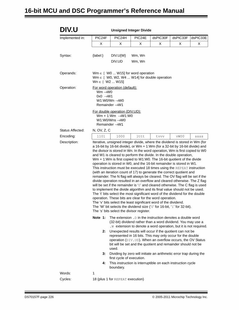
16-bit MCU and DSC Programmer’s Reference Manual
DIV.U Unsigned Integer Divide
Implemented in: PIC24F PIC24H PIC24E dsPIC30F dsPIC33F dsPIC33E
X X X X X X
Syntax: {label:} DIV.U{W} Wm, Wn
DIV.UD Wm, Wn
Operands: Wm ∈ [ W0 ... W15] for word operationWm ∈ [ W0, W2, W4 ... W14] for double operationWn ∈ [ W2 ... W15]
Operation: For word operation (default): Wm → W0 0x0 → W1 W1:W0/Wn → W0 Remainder → W1
For double operation (DIV.UD): Wm + 1:Wm → W1:W0 W1:W0/Wns → W0 Remainder → W1
Status Affected: N, OV, Z, C
Encoding: 1101 1000 1ttt tvvv vW00 ssss
Description: Iterative, unsigned integer divide, where the dividend is stored in Wm (for a 16-bit by 16-bit divide), or Wm + 1:Wm (for a 32-bit by 16-bit divide) and the divisor is stored in Wn. In the word operation, Wm is first copied to W0 and W1 is cleared to perform the divide. In the double operation, Wm + 1:Wm is first copied to W1:W0. The 16-bit quotient of the divide operation is stored in W0, and the 16-bit remainder is stored in W1.This instruction must be executed 18 times using the REPEAT instruction (with an iteration count of 17) to generate the correct quotient and remainder. The N flag will always be cleared. The OV flag will be set if the divide operation resulted in an overflow and cleared otherwise. The Z flag will be set if the remainder is ‘0’ and cleared otherwise. The C flag is used to implement the divide algorithm and its final value should not be used.The ‘t’ bits select the most significant word of the dividend for the double operation. These bits are clear for the word operation.The ‘v’ bits select the least significant word of the dividend.The ‘W’ bit selects the dividend size (‘0’ for 16-bit, ‘1’ for 32-bit).The ‘s’ bits select the divisor register.
Note 1: The extension .D in the instruction denotes a double word (32-bit) dividend rather than a word dividend. You may use a .W extension to denote a word operation, but it is not required.
2: Unexpected results will occur if the quotient can not be represented in 16 bits. This may only occur for the double operation (DIV.UD). When an overflow occurs, the OV Status bit will be set and the quotient and remainder should not be used.
3: Dividing by zero will initiate an arithmetic error trap during the first cycle of execution.
4: This instruction is interruptible on each instruction cycle boundary.
Words: 1
Cycles: 18 (plus 1 for REPEAT execution)
DS70157F-page 226 © 2005-2011 Microchip Technology Inc.

Section 5. Instruction DescriptionsInstruction
Descriptions
5
Example 1: REPEAT #17 ; Execute DIV.U 18 timesDIV.U W2, W4 ; Divide W2 by W4 ; Store quotient to W0, remainder to W1
Before Instruction
AfterInstruction
W0 5555 W0 0040W1 1234 W1 0000W2 8000 W2 8000 W4 0200 W4 0200 SR 0000 SR 0002 (Z = 1)
Example 2: REPEAT #17 ; Execute DIV.UD 18 timesDIV.UD W10, W12 ; Divide W11:W10 by W12 ; Store quotient to W0, remainder to W1
Before Instruction
AfterInstruction
W0 5555 W0 01F2W1 1234 W1 0100
W10 2500 W10 2500 W11 0042 W11 0042 W12 2200 W12 2200
SR 0000 SR 0000
© 2005-2011 Microchip Technology Inc. DS70157F-page 227

16-bit MCU and DSC Programmer’s Reference Manual
DIVF Fractional Divide
Implemented in: PIC24F PIC24H PIC24E dsPIC30F dsPIC33F dsPIC33E
X X X
Syntax: {label:} DIVF Wm, Wn
Operands: Wm ∈ [ W0 ... W15]Wn ∈ [ W2 ... W15]
Operation: 0x0 → W0Wm → W1W1:W0/Wn → W0Remainder → W1
Status Affected: N, OV, Z, C
Encoding: 1101 1001 0ttt t000 0000 ssss
Description: Iterative, signed fractional 16-bit by 16-bit divide, where the dividend is stored in Wm and the divisor is stored in Wn. To perform the operation, W0 is first cleared and Wm is copied to W1. The 16-bit quotient of the divide operation is stored in W0, and the 16-bit remainder is stored in W1. The sign of the remainder will be the same as the sign of the dividend.
This instruction must be executed 18 times using the REPEAT instruction (with an iteration count of 17) to generate the correct quotient and remainder. The N flag will be set if the remainder is negative and cleared otherwise. The OV flag will be set if the divide operation resulted in an overflow and cleared otherwise. The Z flag will be set if the remainder is ‘0’ and cleared otherwise. The C flag is used to implement the divide algorithm and its final value should not be used.
The ‘t’ bits select the dividend register.The ‘s’ bits select the divisor register.
Note 1: For the fractional divide to be effective, Wm must be less than Wn. If Wm is greater than or equal to Wn, unexpected results will occur because the fractional result will be greater than or equal to 1.0. When this occurs, the OV Status bit will be set and the quotient and remainder should not be used.
2: Dividing by zero will initiate an arithmetic error trap during the first cycle of execution.
3: This instruction is interruptible on each instruction cycle boundary.
Words: 1
Cycles: 18 (plus 1 for REPEAT execution)
DS70157F-page 228 © 2005-2011 Microchip Technology Inc.

Section 5. Instruction DescriptionsInstruction
Descriptions
5
Example 1: REPEAT #17 ; Execute DIVF 18 timesDIVF W8, W9 ; Divide W8 by W9 ; Store quotient to W0, remainder to W1
Before Instruction
AfterInstruction
W0 8000 W0 2000W1 1234 W1 0000W8 1000 W8 1000W9 4000 W9 4000 SR 0000 SR 0002 (Z = 1)
Example 2: REPEAT #17 ; Execute DIVF 18 timesDIVF W8, W9 ; Divide W8 by W9 ; Store quotient to W0, remainder to W1
Before Instruction
AfterInstruction
W0 8000 W0 F000W1 1234 W1 0000W8 1000 W8 1000W9 8000 W9 8000 SR 0000 SR 0002 (Z = 1)
Example 3: REPEAT #17 ; Execute DIVF 18 timesDIVF W0, W1 ; Divide W0 by W1 ; Store quotient to W0, remainder to W1
Before Instruction
AfterInstruction
W0 8002 W0 7FFEW1 8001 W1 8002SR 0000 SR 0008 (N = 1)
© 2005-2011 Microchip Technology Inc. DS70157F-page 229

16-bit MCU and DSC Programmer’s Reference Manual
DO Initialize Hardware Loop Literal
Implemented in: PIC24F PIC24H PIC24E dsPIC30F dsPIC33F dsPIC33E
X X
Syntax: {label:} DO #lit14, Expr
Operands: lit14 ∈ [0 ... 16383]Expr may be an absolute address, label or expression.Expr is resolved by the linker to a Slit16, where Slit16 ∈ [-32768 ... +32767].
Operation: PUSH DO shadows (DCOUNT, DOEND, DOSTART)(lit14) → DCOUNT(PC) + 4 → PC(PC) → DOSTART(PC) + (2 * Slit16) → DOENDIncrement DL<2:0> (CORCON<10:8>)
Status Affected: DA
Encoding: 0000 1000 00kk kkkk kkkk kkkk
0000 0000 nnnn nnnn nnnn nnnn
DS70157F-page 230 © 2005-2011 Microchip Technology Inc.

Section 5. Instruction DescriptionsInstruction
Descriptions
5
Description: Initiate a no overhead hardware DO loop, which is executed (lit14 + 1) times. The DO loop begins at the address following the DO instruction, and ends at the address 2 * Slit16 instruction words away. The 14-bit count value (lit14) supports a maximum loop count value of 16384, and the 16-bit offset value (Slit16) supports offsets of 32K instruction words in both directions.When this instruction executes, DCOUNT, DOSTART and DOEND are first PUSHed into their respective shadow registers, and then updated with the new DO loop parameters specified by the instruction. The DO level count, DL<2:0> (CORCON<8:10>), is then incremented. After the DO loop completes execution, the PUSHed DCOUNT, DOSTART and DOEND registers are restored, and DL<2:0> is decremented.
The ‘k’ bits specify the loop count.The ‘n’ bits are a signed literal that specifies the number of instructions that are offset from the PC to the last instruction executed in the loop.
Special Features, Restrictions:The following features and restrictions apply to the DO instruction.1. Using a loop count of ‘0’ will result in the loop being executed one
time.2. Using a loop size of -2, -1 or 0 is invalid. Unexpected results may
occur if these offsets are used.3. The very last two instructions of the DO loop cannot be:
• an instruction which changes program control flow• a DO or REPEAT instructionUnexpected results may occur if any of these instructions are used.
4. If a hard trap occurs in the second to last instruction or third to last instruction of a DO loop, the loop will not function properly. The hard trap includes exceptions of priority level 13 through level 15, inclusive.
Note 1: The DO instruction is interruptible and supports 1 level of hardware nesting. Nesting up to an additional 5 levels may be provided in software by the user. See the specific device family reference manual for details.
2: The linker will convert the specified expression into the offset to be used.
Words: 2
Cycles: 2
Example 1: 002000 LOOP6: DO #5, END6; Initiate DO loop (6 reps)002004 ADD W1, W2, W3; First instruction in loop002006 . . .002008 . . .00200A END6: SUB W2, W3, W4; Last instruction in loop00200C . . .
Before Instruction
After Instruction
PC 00 2000 PC 00 2004DCOUNT 0000 DCOUNT 0005
DOSTART FF FFFF DOSTART 00 2004DOEND FF FFFF DOEND 00 200A
CORCON 0000 CORCON 0100 (DL = 1)SR 0001 (C = 1) SR 0201 (DA, C = 1)
© 2005-2011 Microchip Technology Inc. DS70157F-page 231

16-bit MCU and DSC Programmer’s Reference Manual
Example 2: 01C000 LOOP12: DO #0x160, END12; Init DO loop (353 reps)01C004 DEC W1, W2; First instruction in loop01C006 . . .01C008 . . .01C00A . . .01C00C . . .01C00E CALL _FIR88; Call the FIR88 subroutine01C012 NOP01C014 END12: NOP; Last instruction in loop
; (Required NOP filler)
Before Instruction
After Instruction
PC 01 C000 PC 01 C004DCOUNT 0000 DCOUNT 0160
DOSTART FF FFFF DOSTART 01 C004DOEND FF FFFF DOEND 01 C014
CORCON 0000 CORCON 0100 (DL = 1)SR 0008 (N = 1) SR 0208 (DA, N = 1)
DS70157F-page 232 © 2005-2011 Microchip Technology Inc.

Section 5. Instruction DescriptionsInstruction
Descriptions
5
DO Initialize Hardware Loop Literal
Implemented in: PIC24F PIC24H PIC24E dsPIC30F dsPIC33F dsPIC33E
X
Syntax: {label:} DO #lit15, Expr
Operands: lit15 ∈ [0 ... 32767]Expr may be an absolute address, label or expression.Expr is resolved by the linker to a Slit16, where Slit16 ∈ [-32768 ... +32767].
Operation: PUSH DO shadows (DCOUNT, DOEND, DOSTART)(lit15) → DCOUNT(PC) + 4 → PC(PC) → DOSTART(PC) + (2 * Slit16) → DOENDIncrement DL<2:0> (CORCON<10:8>)
Status Affected: DA
Encoding: 0000 1000 0kkk kkkk kkkk kkkk
0000 0000 nnnn nnnn nnnn nnnn
Description: Initiate a no overhead hardware DO loop, which is executed (lit15 + 1) times. The DO loop begins at the address following the DO instruction, and ends at the address 2 * Slit16 instruction words away. The 15-bit count value (lit15) supports a maximum loop count value of 32768, and the 16-bit offset value (Slit16) supports offsets of 32K instruction words in both directions.
When this instruction executes, DCOUNT, DOSTART and DOEND are first PUSHed into their respective shadow registers, and then updated with the new DO loop parameters specified by the instruction. The DO level count, DL<2:0> bits (CORCON<8:10>), is then incremented. After the DO loop completes execution, the PUSHed DCOUNT, DOSTART and DOEND registers are restored, and DL<2:0> is decremented.
The ‘k’ bits specify the loop count.The ‘n’ bits are a signed literal that specifies the number of instructions that are offset from the PC to the last instruction executed in the loop.
Special Features, Restrictions:The following features and restrictions apply to the DO instruction.1. Using a loop count of ‘0’ will result in the loop being executed one time.2. Using a loop size of -2, -1 or 0 is invalid. Unexpected results may
occur if these offsets are used.3. The very last two instructions of the DO loop cannot be:
• an instruction which changes program control flow• a DO or REPEAT instructionUnexpected results may occur if any of these instructions are used.
4. If a hard trap occurs in the second to last instruction or third to last instruction of a DO loop, the loop will not function properly. The hard trap includes exceptions of priority level 13 through level 15, inclusive.
5. The first instruction of the DO loop cannot be a PSV read or Table read.
Note 1: The DO instruction is interruptible and supports 1 level of hardware nesting. Nesting up to an additional 5 levels may be provided in software by the user. See the specific device family reference manual for details.
2: The linker will convert the specified expression into the offset to be used.
© 2005-2011 Microchip Technology Inc. DS70157F-page 233

16-bit MCU and DSC Programmer’s Reference Manual
Words: 2
Cycles: 2
Example 1: 002000 LOOP6: DO #5, END6; Initiate DO loop (6 reps)002004 ADD W1, W2, W3; First instruction in loop002006 . . .002008 . . .00200A END6: SUB W2, W3, W4; Last instruction in loop00200C . . .
Before Instruction
After Instruction
PC 00 2000 PC 00 2004DCOUNT 0000 DCOUNT 0005
DOSTART FF FFFF DOSTART 00 2004DOEND FF FFFF DOEND 00 200A
CORCON 0000 CORCON 0100 (DL = 1)SR 0001 (C = 1) SR 0201 (DA, C = 1)
Example 2: 01C000 LOOP12: DO #0x160, END12; Init DO loop (353 reps)01C004 DEC W1, W2; First instruction in loop01C006 . . .01C008 . . .01C00A . . .01C00C . . .01C00E CALL _FIR88; Call the FIR88 subroutine01C012 NOP01C014 END12: NOP; Last instruction in loop
; (Required NOP filler)
Before Instruction
After Instruction
PC 01 C000 PC 01 C004DCOUNT 0000 DCOUNT 0160
DOSTART FF FFFF DOSTART 01 C004DOEND FF FFFF DOEND 01 C014
CORCON 0000 CORCON 0100 (DL = 1)SR 0008 (N = 1) SR 0208 (DA, N = 1)
DS70157F-page 234 © 2005-2011 Microchip Technology Inc.

Section 5. Instruction DescriptionsInstruction
Descriptions
5
DO Initialize Hardware Loop Wn
Implemented in: PIC24F PIC24H PIC24E dsPIC30F dsPIC33F dsPIC33E
X X
Syntax: {label:} DO Wn, Expr
Operands: Wn ∈ [W0 ... W15]Expr may be an absolute address, label or expression.Expr is resolved by the linker to a Slit16, where Slit16 ∈ [-32768 ... +32767].
Operation: PUSH Shadows (DCOUNT, DOEND, DOSTART)(Wn<13:0>) → DCOUNT(PC) + 4 → PC(PC) → DOSTART (PC) + (2 * Slit16) → DOENDIncrement DL<2:0> (CORCON<10:8>)
Status Affected: DA
0000 1000 1000 0000 0000 ssss
Encoding: 0000 0000 nnnn nnnn nnnn nnnn
Description: Initiate a no overhead hardware DO loop, which is executed (Wn + 1) times. The DO loop begins at the address following the DO instruction, and ends at the address 2 * Slit16 instruction words away. The lower 14 bits of Wn support a maximum count value of 16384, and the 16-bit offset value (Slit16) supports offsets of 32K instruction words in both directions.
When this instruction executes, DCOUNT, DOSTART and DOEND are first PUSHed into their respective shadow registers, and then updated with the new DO loop parameters specified by the instruction. The DO level count, DL<2:0> (CORCON<8:10>), is then incremented. After the DO loop completes execution, the PUSHed DCOUNT, DOSTART and DOEND registers are restored, and DL<2:0> is decremented.
The ‘s’ bits specify the register Wn that contains the loop count.The ‘n’ bits are a signed literal that specifies the number of instructions that are offset from (PC + 4), which is the last instruction executed in the loop.
Special Features, Restrictions:The following features and restrictions apply to the DO instruction. 1. Using a loop count of ‘0’ will result in the loop being executed one
time.2. Using an offset of -2, -1 or 0 is invalid. Unexpected results may occur
if these offsets are used.3. The very last two instructions of the DO loop cannot be:
• an instruction which changes program control flow• a DO or REPEAT instructionUnexpected results may occur if these last instructions are used.
Note 1: The DO instruction is interruptible and supports 1 level of nesting. Nesting up to an additional 5 levels may be provided in software by the user. See the specific device family reference manual for details.
2: The linker will convert the specified expression into the offset to be used.
Words: 2
Cycles: 2
© 2005-2011 Microchip Technology Inc. DS70157F-page 235

16-bit MCU and DSC Programmer’s Reference Manual
Example 1: 002000 LOOP6: DO W0, END6 ; Initiate DO loop (W0 reps)002004 ADD W1, W2, W3 ; First instruction in loop002006 . . .002008 . . .00200A . . .00200C REPEAT #600200E SUB W2, W3, W4 002010 END6: NOP ; Last instruction in loop ; (Required NOP filler)
Before Instruction
After Instruction
PC 00 2000 PC 00 2004W0 0012 W0 0012
DCOUNT 0000 DCOUNT 0012DOSTART FF FFFF DOSTART 00 2004
DOEND FF FFFF DOEND 00 2010CORCON 0000 CORCON 0100 (DL = 1)
SR 0000 SR 0080 (DA = 1)
Example 2: 002000 LOOPA: DO W7, ENDA ; Initiate DO loop (W7 reps)002004 SWAP W0 ; First instruction in loop002006 . . .002008 . . .00200A . . .002010 ENDA: MOV W1, [W2++] ; Last instruction in loop
Before Instruction
After Instruction
PC 00 2000 PC 00 2004W7 E00F W7 E00F
DCOUNT 0000 DCOUNT 200FDOSTART FF FFFF DOSTART 00 2004
DOEND FF FFFF DOEND 00 2010CORCON 0000 CORCON 0100 (DL = 1)
SR 0000 SR 0080 (DA = 1)
DS70157F-page 236 © 2005-2011 Microchip Technology Inc.
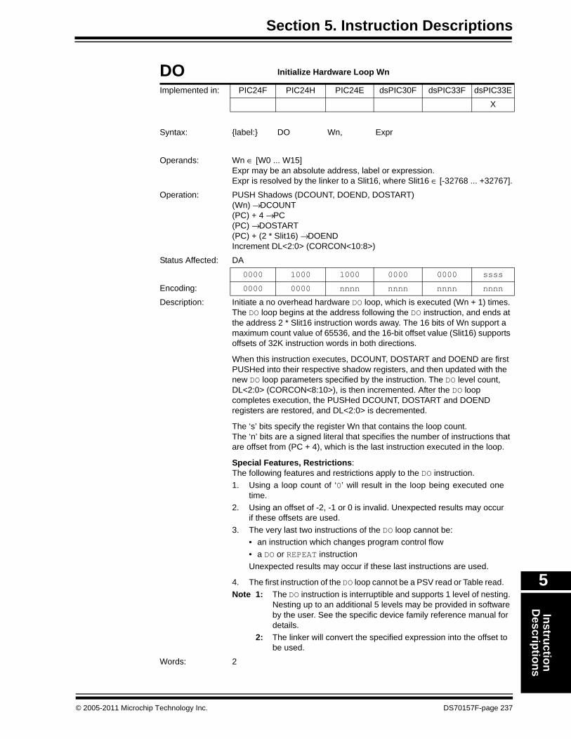
Section 5. Instruction DescriptionsInstruction
Descriptions
5
DO Initialize Hardware Loop Wn
Implemented in: PIC24F PIC24H PIC24E dsPIC30F dsPIC33F dsPIC33E
X
Syntax: {label:} DO Wn, Expr
Operands: Wn ∈ [W0 ... W15]Expr may be an absolute address, label or expression.Expr is resolved by the linker to a Slit16, where Slit16 ∈ [-32768 ... +32767].
Operation: PUSH Shadows (DCOUNT, DOEND, DOSTART)(Wn) → DCOUNT(PC) + 4 → PC(PC) → DOSTART (PC) + (2 * Slit16) → DOENDIncrement DL<2:0> (CORCON<10:8>)
Status Affected: DA
0000 1000 1000 0000 0000 ssss
Encoding: 0000 0000 nnnn nnnn nnnn nnnn
Description: Initiate a no overhead hardware DO loop, which is executed (Wn + 1) times. The DO loop begins at the address following the DO instruction, and ends at the address 2 * Slit16 instruction words away. The 16 bits of Wn support a maximum count value of 65536, and the 16-bit offset value (Slit16) supports offsets of 32K instruction words in both directions.
When this instruction executes, DCOUNT, DOSTART and DOEND are first PUSHed into their respective shadow registers, and then updated with the new DO loop parameters specified by the instruction. The DO level count, DL<2:0> (CORCON<8:10>), is then incremented. After the DO loop completes execution, the PUSHed DCOUNT, DOSTART and DOEND registers are restored, and DL<2:0> is decremented.
The ‘s’ bits specify the register Wn that contains the loop count.The ‘n’ bits are a signed literal that specifies the number of instructions that are offset from (PC + 4), which is the last instruction executed in the loop.
Special Features, Restrictions:The following features and restrictions apply to the DO instruction. 1. Using a loop count of ‘0’ will result in the loop being executed one
time.2. Using an offset of -2, -1 or 0 is invalid. Unexpected results may occur
if these offsets are used.3. The very last two instructions of the DO loop cannot be:
• an instruction which changes program control flow• a DO or REPEAT instructionUnexpected results may occur if these last instructions are used.
4. The first instruction of the DO loop cannot be a PSV read or Table read.Note 1: The DO instruction is interruptible and supports 1 level of nesting.
Nesting up to an additional 5 levels may be provided in software by the user. See the specific device family reference manual for details.
2: The linker will convert the specified expression into the offset to be used.
Words: 2
© 2005-2011 Microchip Technology Inc. DS70157F-page 237
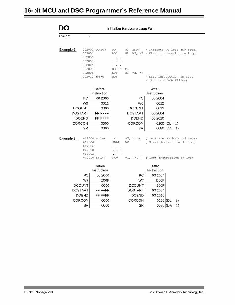
16-bit MCU and DSC Programmer’s Reference Manual
Cycles: 2
DO Initialize Hardware Loop Wn
Example 1: 002000 LOOP6: DO W0, END6 ; Initiate DO loop (W0 reps)002004 ADD W1, W2, W3 ; First instruction in loop002006 . . .002008 . . .00200A . . .00200C REPEAT #600200E SUB W2, W3, W4 002010 END6: NOP ; Last instruction in loop ; (Required NOP filler)
Before Instruction
After Instruction
PC 00 2000 PC 00 2004W0 0012 W0 0012
DCOUNT 0000 DCOUNT 0012DOSTART FF FFFF DOSTART 00 2004
DOEND FF FFFF DOEND 00 2010CORCON 0000 CORCON 0100 (DL = 1)
SR 0000 SR 0080 (DA = 1)
Example 2: 002000 LOOPA: DO W7, ENDA ; Initiate DO loop (W7 reps)002004 SWAP W0 ; First instruction in loop002006 . . .002008 . . .00200A . . .002010 ENDA: MOV W1, [W2++] ; Last instruction in loop
Before Instruction
After Instruction
PC 00 2000 PC 00 2004W7 E00F W7 E00F
DCOUNT 0000 DCOUNT 200FDOSTART FF FFFF DOSTART 00 2004
DOEND FF FFFF DOEND 00 2010CORCON 0000 CORCON 0100 (DL = 1)
SR 0000 SR 0080 (DA = 1)
DS70157F-page 238 © 2005-2011 Microchip Technology Inc.

Section 5. Instruction DescriptionsInstruction
Descriptions
5
ED Euclidean Distance (No Accumulate)
Implemented in: PIC24F PIC24H PIC24E dsPIC30F dsPIC33F dsPIC33E
X X X
Syntax: {label:} ED Wm * Wm, Acc, [Wx], [Wy], Wxd
[Wx] + = kx, [Wy] + = ky,
[Wx] – = kx, [Wy] – = ky,
[W9 + W12],
[W11 + W12],
Operands: Acc ∈ [A,B]Wm * Wm ∈ [W4 * W4, W5 * W5, W6 * W6, W7 * W7]Wx ∈ [W8, W9]; kx ∈ [-6, -4, -2, 2, 4, 6]Wy ∈ [W10, W11]; ky ∈ [-6, -4, -2, 2, 4, 6]Wxd ∈ [W4 ... W7]
Operation: (Wm) * (Wm) → Acc(A or B)([Wx] – [Wy]) → Wxd(Wx) + kx → Wx(Wy) + ky → Wy
Status Affected: OA, OB, OAB, SA, SB, SAB
Encoding: 1111 00mm A1xx 00ii iijj jj11
Description: Compute the square of Wm, and compute the difference of the prefetch values specified by [Wx] and [Wy]. The results of Wm * Wm are sign-extended to 40 bits and stored in the specified accumulator. The results of [Wx] – [Wy] are stored in Wxd, which may be the same as Wm.
Operands Wx, Wxd and Wyd specify the prefetch operations which support indirect and register offset addressing as described in Section 4.14.1 “MAC Prefetches”.
The ‘m’ bits select the operand register Wm for the square.The ‘A’ bit selects the accumulator for the result.The ‘x’ bits select the prefetch difference Wxd destination.The ‘i’ bits select the Wx prefetch operation.The ‘j’ bits select the Wy prefetch operation.
Words: 1
Cycles: 1Example 1: ED W4*W4, A, [W8]+=2, [W10]-=2, W4 ; Square W4 to ACCA
; [W8]-[W10] to W4; Post-increment W8 ; Post-decrement W10
Before Instruction
After Instruction
W4 009A W4 0057W8 1100 W8 1102
W10 2300 W10 22FEACCA 00 3D0A 0000 ACCA 00 0000 5CA4
Data 1100 007F Data 1100 007FData 2300 0028 Data 2300 0028
SR 0000 SR 0000
© 2005-2011 Microchip Technology Inc. DS70157F-page 239
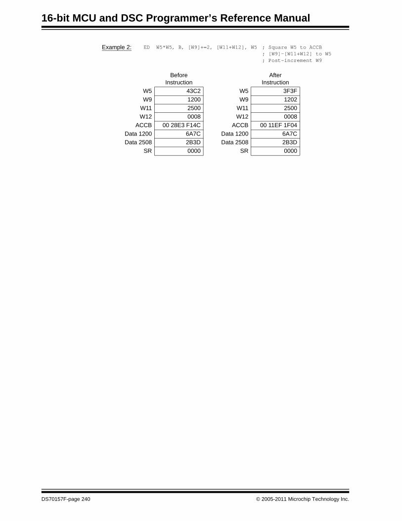
16-bit MCU and DSC Programmer’s Reference Manual
Example 2: ED W5*W5, B, [W9]+=2, [W11+W12], W5 ; Square W5 to ACCB; [W9]-[W11+W12] to W5; Post-increment W9
Before Instruction
After Instruction
W5 43C2 W5 3F3FW9 1200 W9 1202
W11 2500 W11 2500W12 0008 W12 0008
ACCB 00 28E3 F14C ACCB 00 11EF 1F04Data 1200 6A7C Data 1200 6A7CData 2508 2B3D Data 2508 2B3D
SR 0000 SR 0000
DS70157F-page 240 © 2005-2011 Microchip Technology Inc.

Section 5. Instruction DescriptionsInstruction
Descriptions
5
EDAC Euclidean Distance
Implemented in: PIC24F PIC24H PIC24E dsPIC30F dsPIC33F dsPIC33EX X X
Syntax: {label:} EDAC Wm * Wm, Acc, [Wx], [Wy], Wxd[Wx] + = kx,
[Wy] + = ky,
[Wx] – = kx, [Wy] – = ky,[W9 + W12],
[W11 + W12],
Operands: Acc ∈ [A,B]Wm * Wm ∈ [W4 * W4, W5 * W5, W6 * W6, W7 * W7]Wx ∈ [W8, W9]; kx ∈ [-6, -4, -2, 2, 4, 6] Wy ∈ [W10, W11]; ky ∈ [-6, -4, -2, 2, 4, 6] Wxd ∈ [W4 ... W7]
Operation: (Acc(A or B)) + (Wm) * (Wm) → Acc(A or B)([Wx] – [Wy]) → Wxd(Wx) + kx → Wx(Wy) + ky → Wy
Status Affected: OA, OB, OAB, SA, SB, SABEncoding: 1111 00mm A1xx 00ii iijj jj10
Description: Compute the square of Wm, and also the difference of the prefetch values specified by [Wx] and [Wy]. The results of Wm * Wm are sign-extended to 40 bits and added to the specified accumulator. The results of [Wx] – [Wy] are stored in Wxd, which may be the same as Wm.
Operands Wx, Wxd and Wyd specify the prefetch operations which support indirect and register offset addressing as described in Section 4.14.1 “MAC Prefetches”.
The ‘m’ bits select the operand register Wm for the square.The ‘A’ bit selects the accumulator for the result. The ‘x’ bits select the prefetch difference Wxd destination.The ‘i’ bits select the Wx prefetch operation.The ‘j’ bits select the Wy prefetch operation.
Words: 1Cycles: 1
Example 1: EDAC W4*W4, A, [W8]+=2, [w10]-=2, W4 ; Square W4 and; add to ACCA; [W8]-[W10] to W4; Post-increment W8 ; Post-decrement W10
Before Instruction
After Instruction
W4 009A W4 0057W8 1100 W8 1102
W10 2300 W10 22FEACCA 00 3D0A 3D0A ACCA 00 3D0A 99AE
Data 1100 007F Data 1100 007FData 2300 0028 Data 2300 0028
SR 0000 SR 0000
© 2005-2011 Microchip Technology Inc. DS70157F-page 241

16-bit MCU and DSC Programmer’s Reference Manual
Example 2: EDAC W5*W5, B, [w9]+=2, [W11+W12], W5 ; Square W5 and; add to ACCB; [W9]-[W11+W12] to W5; Post-increment W9
Before Instruction
After Instruction
W5 43C2 W5 3F3FW9 1200 W9 1202
W11 2500 W11 2500W12 0008 W12 0008
ACCB 00 28E3 F14C ACCB 00 3AD3 1050Data 1200 6A7C Data 1200 6A7CData 2508 2B3D Data 2508 2B3D
SR 0000 SR 0000
DS70157F-page 242 © 2005-2011 Microchip Technology Inc.

Section 5. Instruction DescriptionsInstruction
Descriptions
5
EXCH Exchange Wns and Wnd
Implemented in: PIC24F PIC24H PIC24E dsPIC30F dsPIC33F dsPIC33E
X X X X X X
Syntax: {label:} EXCH Wns, Wnd
Operands: Wns ∈ [W0 ... W15]Wnd ∈ [W0 ... W15]
Operation: (Wns) ↔ (Wnd)
Status Affected: None
Encoding: 1111 1101 0000 0ddd d000 ssss
Description: Exchange the word contents of two working registers. Register direct addressing must be used for Wns and Wnd.
The ‘d’ bits select the address of the first register.The ‘s’ bits select the address of the second register.
Note: This instruction only executes in Word mode.
Words: 1
Cycles: 1
Example 1: EXCH W1, W9 ; Exchange the contents of W1 and W9
BeforeInstruction
AfterInstruction
W1 55FF W1 A3A3W9 A3A3 W9 55FFSR 0000 SR 0000
Example 2: EXCH W4, W5 ; Exchange the contents of W4 and W5
BeforeInstruction
AfterInstruction
W4 ABCD W4 4321W5 4321 W5 ABCDSR 0000 SR 0000
© 2005-2011 Microchip Technology Inc. DS70157F-page 243
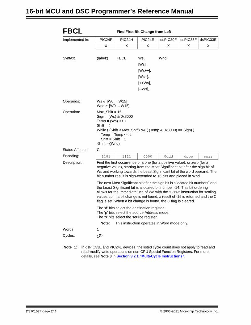
16-bit MCU and DSC Programmer’s Reference Manual
FBCL Find First Bit Change from Left
Implemented in: PIC24F PIC24H PIC24E dsPIC30F dsPIC33F dsPIC33E
X X X X X X
Syntax: {label:} FBCL Ws, Wnd
[Ws],
[Ws++],
[Ws--],
[++Ws],
[--Ws],
Operands: Ws ∈ [W0 ... W15]Wnd ∈ [W0 ... W15]
Operation: Max_Shift = 15Sign = (Ws) & 0x8000Temp = (Ws) << 1Shift = 0While ( (Shift < Max_Shift) && ( (Temp & 0x8000) == Sign) ) Temp = Temp << 1 Shift = Shift + 1-Shift → (Wnd)
Status Affected: C
Encoding: 1101 1111 0000 0ddd dppp ssss
Description: Find the first occurrence of a one (for a positive value), or zero (for a negative value), starting from the Most Significant bit after the sign bit of Ws and working towards the Least Significant bit of the word operand. The bit number result is sign-extended to 16 bits and placed in Wnd.
The next Most Significant bit after the sign bit is allocated bit number 0 and the Least Significant bit is allocated bit number -14. This bit ordering allows for the immediate use of Wd with the SFTAC instruction for scaling values up. If a bit change is not found, a result of -15 is returned and the C flag is set. When a bit change is found, the C flag is cleared.
The ‘d’ bits select the destination register.The ‘p’ bits select the source Address mode.The ‘s’ bits select the source register.
Note: This instruction operates in Word mode only.
Words: 1
Cycles: 1(1)
Note 1: In dsPIC33E and PIC24E devices, the listed cycle count does not apply to read and read-modify-write operations on non-CPU Special Function Registers. For more details, see Note 3 in Section 3.2.1 “Multi-Cycle Instructions”.
DS70157F-page 244 © 2005-2011 Microchip Technology Inc.

Section 5. Instruction DescriptionsInstruction
Descriptions
5
Example 1: FBCL W1, W9 ; Find 1st bit change from left in W1; and store result to W9
Before Instruction
After Instruction
W1 55FF W1 55FFW9 FFFF W9 0000SR 0000 SR 0000
Example 2: FBCL W1, W9 ; Find 1st bit change from left in W1; and store result to W9
Before Instruction
After Instruction
W1 FFFF W1 FFFFW9 BBBB W9 FFF1SR 0000 SR 0001 (C = 1)
Example 3: FBCL [W1++], W9 ; Find 1st bit change from left in [W1] ; and store result to W9; Post-increment W1
Before Instruction
After Instruction
W1 2000 W1 2002W9 BBBB W9 FFF9
Data 2000 FF0A Data 2000 FF0ASR 0000 SR 0000
© 2005-2011 Microchip Technology Inc. DS70157F-page 245

16-bit MCU and DSC Programmer’s Reference Manual
FF1L Find First One from Left
Implemented in: PIC24F PIC24H PIC24E dsPIC30F dsPIC33F dsPIC33E
X X X X X X
Syntax: {label:} FF1L Ws, Wnd
[Ws],
[Ws++],
[Ws--],
[++Ws],
[--Ws],
Operands: Ws ∈ [W0 ... W15]Wnd ∈ [W0 ... W15]
Operation: Max_Shift = 17Temp = (Ws)Shift = 1While ( (Shift < Max_Shift) && !(Temp & 0x8000) ) Temp = Temp << 1 Shift = Shift + 1If (Shift == Max_Shift) 0 → (Wnd)Else Shift → (Wnd)
Status Affected: C
Encoding: 1100 1111 1000 0ddd dppp ssss
Description: Finds the first occurrence of a ‘1’ starting from the Most Significant bit of Ws and working towards the Least Significant bit of the word operand. The bit number result is zero-extended to 16 bits and placed in Wnd.
Bit numbering begins with the Most Significant bit (allocated number 1) and advances to the Least Significant bit (allocated number 16). A result of zero indicates a ‘1’ was not found, and the C flag will be set. If a ‘1’ is found, the C flag is cleared.
The ‘d’ bits select the destination register.The ‘p’ bits select the source Address mode.The ‘s’ bits select the source register.
Note: This instruction operates in Word mode only.
Words: 1
Cycles: 1(1)
Note 1: In dsPIC33E and PIC24E devices, the listed cycle count does not apply to read and read-modify-write operations on non-CPU Special Function Registers. For more details, see Note 3 in Section 3.2.1 “Multi-Cycle Instructions”.
DS70157F-page 246 © 2005-2011 Microchip Technology Inc.

Section 5. Instruction DescriptionsInstruction
Descriptions
5
Example 1: FF1L W2, W5 ; Find the 1st one from the left in W2 ; and store result to W5
Before Instruction
After Instruction
W2 000A W2 000AW5 BBBB W5 000DSR 0000 SR 0000
Example 2: FF1L [W2++], W5 ; Find the 1st one from the left in [W2] ; and store the result to W5; Post-increment W2
Before Instruction
After Instruction
W2 2000 W2 2002W5 BBBB W5 0000
Data 2000 0000 Data 2000 0000SR 0000 SR 0001 (C = 1)
© 2005-2011 Microchip Technology Inc. DS70157F-page 247

16-bit MCU and DSC Programmer’s Reference Manual
FF1R Find First One from Right
Implemented in: PIC24F PIC24H PIC24E dsPIC30F dsPIC33F dsPIC33E
X X X X X X
Syntax: {label:} FF1R Ws, Wnd
[Ws],
[Ws++],
[Ws--],
[++Ws],
[--Ws],
Operands: Ws ∈ [W0 ... W15]Wnd ∈ [W0 ... W15]
Operation: Max_Shift = 17Temp = (Ws)Shift = 1While ( (Shift < Max_Shift) && !(Temp & 0x1) ) Temp = Temp >> 1 Shift = Shift + 1If (Shift == Max_Shift) 0 → (Wnd)Else Shift → (Wnd)
Status Affected: C
Encoding: 1100 1111 0000 0ddd dppp ssss
Description: Finds the first occurrence of a ‘1’ starting from the Least Significant bit of Ws and working towards the Most Significant bit of the word operand. The bit number result is zero-extended to 16 bits and placed in Wnd.
Bit numbering begins with the Least Significant bit (allocated number 1) and advances to the Most Significant bit (allocated number 16). A result of zero indicates a ‘1’ was not found, and the C flag will be set. If a ‘1’ is found, the C flag is cleared.
The ‘d’ bits select the destination register.The ‘p’ bits select the source Address mode.The ‘s’ bits select the source register.
Note: This instruction operates in Word mode only.
Words: 1
Cycles: 1(1)
Note 1: In dsPIC33E and PIC24E devices, the listed cycle count does not apply to read and read-modify-write operations on non-CPU Special Function Registers. For more details, see Note 3 in Section 3.2.1 “Multi-Cycle Instructions”.
DS70157F-page 248 © 2005-2011 Microchip Technology Inc.

Section 5. Instruction DescriptionsInstruction
Descriptions
5
Example 1: FF1R W1, W9 ; Find the 1st one from the right in W1 ; and store the result to W9
Before Instruction
After Instruction
W1 000A W1 000AW9 BBBB W9 0002SR 0000 SR 0000
Example 2: FF1R [W1++], W9 ; Find the 1st one from the right in [W1] ; and store the result to W9; Post-increment W1
Before Instruction
After Instruction
W1 2000 W1 2002W9 BBBB W9 0010
Data 2000 8000 Data 2000 8000SR 0000 SR 0000
© 2005-2011 Microchip Technology Inc. DS70157F-page 249

16-bit MCU and DSC Programmer’s Reference Manual
GOTO Unconditional Jump
Implemented in: PIC24F PIC24H PIC24E dsPIC30F dsPIC33F dsPIC33E
X X X X X X
Syntax: {label:} GOTO Expr
Operands: Expr may be label or expression (but not a literal).Expr is resolved by the linker to a lit23, where lit23 ∈ [0 ... 8388606].
Operation: lit23 → PCNOP → Instruction Register
Status Affected: None
Encoding:
1st word 0000 0100 nnnn nnnn nnnn nnn0
2nd word 0000 0000 0000 0000 0nnn nnnn
Description: Unconditional jump to anywhere within the 4M instruction word program memory range. The PC is loaded with the 23-bit literal specified in the instruction. Since the PC must always reside on an even address boundary, lit23<0> is ignored.
The ‘n’ bits form the target address.
Note: The linker will resolve the specified expression into the lit23 to be used.
Words: 2
Cycles: 2 (PIC24F, PIC24H, dsPIC30F, dsPIC33F)4 (PIC24E, dsPIC33E)
Example 1: 026000 GOTO _THERE026004 MOV W0, W1 . ... . ...027844 _THERE: MOV #0x400, W2027846 ...
; Jump to _THERE
; Code execution; resumes here
Before Instruction
After Instruction
PC 02 6000 PC 02 7844SR 0000 SR 0000
Example 2: 000100 _code: ... . ...026000 GOTO _code+2026004 ...
; start of code
; Jump to _code+2
Before Instruction
After Instruction
PC 02 6000 PC 00 0102SR 0000 SR 0000
DS70157F-page 250 © 2005-2011 Microchip Technology Inc.
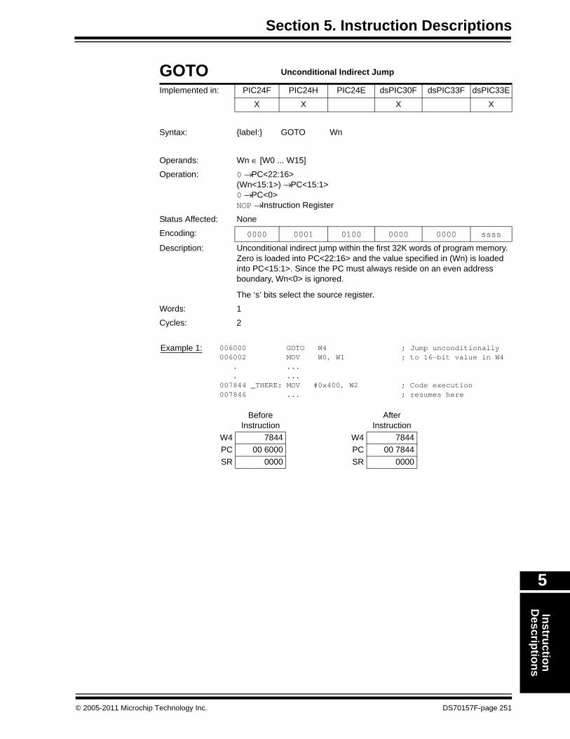
Section 5. Instruction DescriptionsInstruction
Descriptions
5
GOTO Unconditional Indirect Jump
Implemented in: PIC24F PIC24H PIC24E dsPIC30F dsPIC33F dsPIC33E
X X X X
Syntax: {label:} GOTO Wn
Operands: Wn ∈ [W0 ... W15]
Operation: 0 → PC<22:16>(Wn<15:1>) → PC<15:1>0 → PC<0>NOP → Instruction Register
Status Affected: None
Encoding: 0000 0001 0100 0000 0000 ssss
Description: Unconditional indirect jump within the first 32K words of program memory. Zero is loaded into PC<22:16> and the value specified in (Wn) is loaded into PC<15:1>. Since the PC must always reside on an even address boundary, Wn<0> is ignored.
The ‘s’ bits select the source register.
Words: 1
Cycles: 2
Example 1: 006000 GOTO W4006002 MOV W0, W1 . ... . ...007844 _THERE: MOV #0x400, W2007846 ...
; Jump unconditionally; to 16-bit value in W4
; Code execution; resumes here
Before Instruction
After Instruction
W4 7844 W4 7844PC 00 6000 PC 00 7844SR 0000 SR 0000
© 2005-2011 Microchip Technology Inc. DS70157F-page 251

16-bit MCU and DSC Programmer’s Reference Manual
GOTO Unconditional Indirect Jump
Implemented in: PIC24F PIC24H PIC24E dsPIC30F dsPIC33F dsPIC33E
X X
Syntax: {label:} GOTO Wn
Operands: Wn ∈ [W0 ... W15]
Operation: 0 → PC<22:16>(Wn<15:1>) → PC<15:1>0 → PC<0>NOP → Instruction Register
Status Affected: None
Encoding: 0000 0001 0000 0100 0000 ssss
Description: Unconditional indirect jump within the first 32K words of program memory. Zero is loaded into PC<22:16> and the value specified in (Wn) is loaded into PC<15:1>. Since the PC must always reside on an even address boundary, Wn<0> is ignored.
The ‘s’ bits select the source register.
Words: 1
Cycles: 4
Example 1: 006000 GOTO W4006002 MOV W0, W1 . ... . ...007844 _THERE: MOV #0x400, W2007846 ...
; Jump unconditionally; to 16-bit value in W4
; Code execution; resumes here
Before Instruction
After Instruction
W4 7844 W4 7844PC 00 6000 PC 00 7844SR 0000 SR 0000
DS70157F-page 252 © 2005-2011 Microchip Technology Inc.

Section 5. Instruction DescriptionsInstruction
Descriptions
5
GOTO.L Unconditional Indirect Jump Long
Implemented in: PIC24F PIC24H PIC24E dsPIC30F dsPIC33F dsPIC33E
X X
Syntax: {label:} GOTO.L Wn
Operands: Wn ∈ [W0, W2, W4, W6, W8, W10, W12]
Operation: PC<23> → PC<23> (see text); (Wn+1)<6:0> → PC<22:16>; (Wn) → PC<15:0>r
Status Affected: None
Encoding: 0000 0001 1www w100 0000 ssss
Description: Unconditional indirect jump to any user program memory address.
The LS 7-bits of (Wn+1) are loaded in PC<22:16>, and the 16-bit value (Wn) is loaded into PC<15:0>.PC<23> is not modified by this instruction.The contents of (Wn+1)<15:7> are ignored.The value of Wn<0> is also ignored and PC<0> is always set to 0.GOTO is a two-cycle instruction.The ‘s’ bits select the address of the Wn source register.The ‘w’ bits specify the address of the Wn+1 source register.
Words: 1
Cycles: 4
Example 1: 026000 GOTO.L W4026004 MOV W0, W1 . ... . ...026844 _FIR: MOV #0x400, W2026846 ...
; Call _FIR subroutine
; _FIR subroutine start
Before Instruction
After Instruction
PC 02 6000 PC 02 6844W4 6844 W4 6844W5 0002 W5 0002
W15 A268 W15 A26CData A268 FFFF Data A268 6004Data A26A FFFF Data A26A 0002
SR 0000 SR 0000
© 2005-2011 Microchip Technology Inc. DS70157F-page 253

16-bit MCU and DSC Programmer’s Reference Manual
INC Increment f
Implemented in: PIC24F PIC24H PIC24E dsPIC30F dsPIC33F dsPIC33E
X X X X X X
Syntax: {label:} INC{.B} f {,WREG}
Operands: f ∈ [0 ... 8191]
Operation: (f) + 1 → destination designated by D
Status Affected: DC, N, OV, Z, C
Encoding: 1110 1100 0BDf ffff ffff ffff
Description: Add one to the contents of the file register, and place the result in the destination register. The optional WREG operand determines the destination register. If WREG is specified, the result is stored in WREG. If WREG is not specified, the result is stored in the file register.
The ‘B’ bit selects byte or word operation (‘0’ for word, ‘1’ for byte).The ‘D’ bit selects the destination (‘0’ for WREG, ‘1’ for file register).The ‘f’ bits select the address of the file register.
Note 1: The extension .B in the instruction denotes a byte operation rather than a word operation. You may use a .W extension to denote a word operation, but it is not required.
2: The WREG is set to working register W0.
Words: 1
Cycles: 1(1)
Note 1: In dsPIC33E and PIC24E devices, the listed cycle count does not apply to read and read-modify-write operations on non-CPU Special Function Registers. For more details, see Note 3 in Section 3.2.1 “Multi-Cycle Instructions”.
Example 1: INC.B 0x1000 ; Increment 0x1000 (Byte mode)
Before Instruction
After Instruction
Data 1000 8FFF Data 1000 8F00SR 0000 SR 0101 (DC, C = 1)
Example 2: INC 0x1000, WREG ; Increment 0x1000 and store to WREG ; (Word mode)
Before Instruction
After Instruction
WREG ABCD WREG 9000Data 1000 8FFF Data 1000 8FFF
SR 0000 SR 0108 (DC, N = 1)
DS70157F-page 254 © 2005-2011 Microchip Technology Inc.

Section 5. Instruction DescriptionsInstruction
Descriptions
5
INC Increment Ws
Implemented in: PIC24F PIC24H PIC24E dsPIC30F dsPIC33F dsPIC33E
X X X X X X
Syntax: {label:} INC{.B} Ws, Wd
[Ws], [Wd]
[Ws++], [Wd++]
[Ws--], [Wd--]
[++Ws], [++Wd]
[--Ws], [--Wd]
Operands: Ws ∈ [W0 ... W15]Wd ∈ [W0 ... W15]
Operation: (Ws) + 1 → Wd
Status Affected: DC, N, OV, Z, C
Encoding: 1110 1000 0Bqq qddd dppp ssss
Description: Add 1 to the contents of the source register Ws and place the result in the destination register Wd. Register direct or indirect addressing may be used for Ws and Wd.
The ‘B’ bit selects byte or word operation (‘0’ for word, ‘1’ for byte).The ‘q’ bits select the destination Address mode.The ‘d’ bits select the destination register.The ‘p’ bits select the source Address mode.The ‘s’ bits select the source register.
Note: The extension .B in the instruction denotes a byte operation rather than a word operation. You may use a .W extension to denote a word operation, but it is not required.
Words: 1
Cycles: 1(1)
Note 1: In dsPIC33E and PIC24E devices, the listed cycle count does not apply to read and read-modify-write operations on non-CPU Special Function Registers. For more details, see Note 3 in Section 3.2.1 “Multi-Cycle Instructions”.
Example 1: INC.B W1, [++W2] ; Pre-increment W2 ; Increment W1 and store to W2 ; (Byte mode)
Before Instruction
After Instruction
W1 FF7F W1 FF7FW2 2000 W2 2001
Data 2000 ABCD Data 2000 80CDSR 0000 SR 010C (DC, N, OV = 1)
© 2005-2011 Microchip Technology Inc. DS70157F-page 255
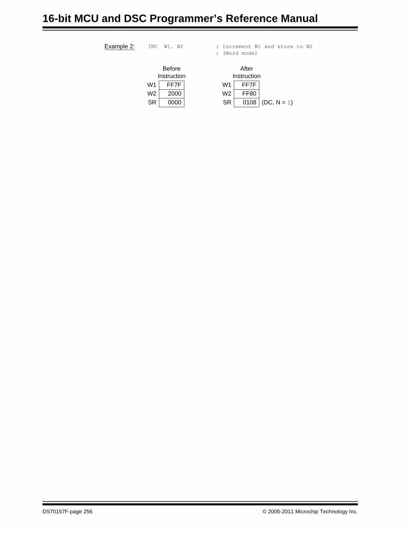
16-bit MCU and DSC Programmer’s Reference Manual
Example 2: INC W1, W2 ; Increment W1 and store to W2 ; (Word mode)
Before Instruction
After Instruction
W1 FF7F W1 FF7FW2 2000 W2 FF80SR 0000 SR 0108 (DC, N = 1)
DS70157F-page 256 © 2005-2011 Microchip Technology Inc.

Section 5. Instruction DescriptionsInstruction
Descriptions
5
INC2 Increment f by 2
Implemented in: PIC24F PIC24H PIC24E dsPIC30F dsPIC33F dsPIC33E
X X X X X X
Syntax: {label:} INC2{.B} f {,WREG}
Operands: f ∈ [0 ... 8191]
Operation: (f) + 2 → destination designated by D
Status Affected: DC, N, OV, Z, C
Encoding: 1110 1100 1BDf ffff ffff ffff
Description: Add 2 to the contents of the file register and place the result in the destination register. The optional WREG operand determines the destination register. If WREG is specified, the result is stored in WREG. If WREG is not specified, the result is stored in the file register.
The ‘B’ bit selects byte or word operation (‘0’ for word, ‘1’ for byte).The ‘D’ bit selects the destination (‘0’ for WREG, ‘1’ for file register).The ‘f’ bits select the address of the file register.
Note: The extension .B in the instruction denotes a byte operation rather than a word operation. You may use a .W extension to denote a word operation, but it is not required.
Words: 1
Cycles: 1(1)
Note 1: In dsPIC33E and PIC24E devices, the listed cycle count does not apply to read and read-modify-write operations on non-CPU Special Function Registers. For more details, see Note 3 in Section 3.2.1 “Multi-Cycle Instructions”.
Example 1: INC2.B 0x1000 ; Increment 0x1000 by 2 ; (Byte mode)
Before Instruction
After Instruction
Data 1000 8FFF Data 1000 8F01SR 0000 SR 0101 (DC, C = 1)
Example 2: INC2 0x1000, WREG ; Increment 0x1000 by 2 and store to WREG ; (Word mode)
Before Instruction
After Instruction
WREG ABCD WREG 9001Data 1000 8FFF Data 1000 8FFF
SR 0000 SR 0108 (DC, N = 1)
© 2005-2011 Microchip Technology Inc. DS70157F-page 257

16-bit MCU and DSC Programmer’s Reference Manual
INC2 Increment Ws by 2
Implemented in: PIC24F PIC24H PIC24E dsPIC30F dsPIC33F dsPIC33E
X X X X X X
Syntax: {label:} INC2{.B} Ws, Wd
[Ws], [Wd]
[Ws++], [Wd++]
[Ws--], [Wd--]
[++Ws], [++Wd]
[--Ws], [--Wd]
Operands: Ws ∈ [W0 ... W15]Wd ∈ [W0 ... W15]
Operation: (Ws) + 2 → Wd
Status Affected: DC, N, OV, Z, C
Encoding: 1110 1000 1Bqq qddd dppp ssss
Description: Add 2 to the contents of the source register Ws and place the result in the destination register Wd. Register direct or indirect addressing may be used for Ws and Wd.
The ‘B’ bit selects byte or word operation (‘0’ for word, ‘1’ for byte).The ‘q’ bits select the destination Address mode.The ‘d’ bits select the destination register.The ‘p’ bits select the source Address mode.The ‘s’ bits select the source register.
Note: The extension .B in the instruction denotes a byte operation rather than a word operation. You may use a .W extension to denote a word operation, but it is not required.
Words: 1
Cycles: 1(1)
Note 1: In dsPIC33E and PIC24E devices, the listed cycle count does not apply to read and read-modify-write operations on non-CPU Special Function Registers. For more details, see Note 3 in Section 3.2.1 “Multi-Cycle Instructions”.
Example 1: INC2.B W1, [++W2] ; Pre-increment W2 ; Increment by 2 and store to W1 ; (Byte mode)
Before Instruction
After Instruction
W1 FF7F W1 FF7FW2 2000 W2 2001
Data 2000 ABCD Data 2000 81CDSR 0000 SR 010C (DC, N, OV = 1)
DS70157F-page 258 © 2005-2011 Microchip Technology Inc.

Section 5. Instruction DescriptionsInstruction
Descriptions
5
Example 2: INC2 W1, W2 ; Increment W1 by 2 and store to W2 ; (word mode)
Before Instruction
After Instruction
W1 FF7F W1 FF7FW2 2000 W2 FF81SR 0000 SR 0108 (DC, N = 1)
© 2005-2011 Microchip Technology Inc. DS70157F-page 259

16-bit MCU and DSC Programmer’s Reference Manual
IOR Inclusive OR f and WREG
Implemented in: PIC24F PIC24H PIC24E dsPIC30F dsPIC33F dsPIC33E
X X X X X X
Syntax: {label:} IOR{.B} f {,WREG}
Operands: f ∈ [0 ... 8191]
Operation: (f).IOR.(WREG) → destination designated by D
Status Affected: N, Z
Encoding: 1011 0111 0BDf ffff ffff ffff
Description: Compute the logical inclusive OR operation of the contents of the working register WREG and the contents of the file register and place the result in the destination register. The optional WREG operand determines the destination register. If WREG is specified, the result is stored in WREG. If WREG is not specified, the result is stored in the file register.
The ‘B’ bit selects byte or word operation (‘0’ for word, ‘1’ for byte).The ‘D’ bit selects the destination (‘0’ for WREG, ‘1’ for file register).The ‘f’ bits select the address of the file register.
Note 1: The extension .B in the instruction denotes a byte operation rather than a word operation. You may use a .W extension to denote a word operation, but it is not required.
2: The WREG is set to working register W0.
Words: 1
Cycles: 1(1)
Note 1: In dsPIC33E and PIC24E devices, the listed cycle count does not apply to read and read-modify-write operations on non-CPU Special Function Registers. For more details, see Note 3 in Section 3.2.1 “Multi-Cycle Instructions”.
Example 1: IOR.B 0x1000 ; IOR WREG to (0x1000) (Byte mode) ; (Byte mode)
Before Instruction
After Instruction
WREG 1234 WREG 1234Data 1000 FF00 Data 1000 FF34
SR 0000 SR 0000
Example 2: IOR 0x1000, WREG ; IOR (0x1000) to WREG ; (Word mode)
Before Instruction
After Instruction
WREG 1234 WREG 1FBFData 1000 0FAB Data 1000 0FAB
SR 0008 (N = 1) SR 0000
DS70157F-page 260 © 2005-2011 Microchip Technology Inc.

Section 5. Instruction DescriptionsInstruction
Descriptions
5
IOR Inclusive OR Literal and Wn
Implemented in: PIC24F PIC24H PIC24E dsPIC30F dsPIC33F dsPIC33E
X X X X X X
Syntax: {label:} IOR{.B} #lit10, Wn
Operands: lit10 ∈ [0 ... 255] for byte operationlit10 ∈ [0 ... 1023] for word operationWn ∈ [W0 ... W15]
Operation: lit10.IOR.(Wn) → Wn
Status Affected: N, Z
Encoding: 1011 0011 0Bkk kkkk kkkk dddd
Description: Compute the logical inclusive OR operation of the 10-bit literal operand and the contents of the working register Wn and place the result back into the working register Wn.
The ‘B’ bit selects byte or word operation (‘0’ for word, ‘1’ for byte).The ‘k’ bits specify the literal operand.The ‘d’ bits select the address of the working register.
Note 1: The extension .B in the instruction denotes a byte operation rather than a word operation. You may use a .W extension to denote a word operation, but it is not required.
2: For byte operations, the literal must be specified as an unsigned value [0:255]. See Section 4.6 “Using 10-bit Literal Operands” for information on using 10-bit literal operands in Byte mode.
Words: 1
Cycles: 1
Example 1: IOR.B #0xAA, W9 ; IOR 0xAA to W9 ; (Byte mode)
Before Instruction
After Instruction
W9 1234 W9 12BESR 0000 SR 0008 (N = 1)
Example 2: IOR #0x2AA, W4 ; IOR 0x2AA to W4 ; (Word mode)
Before Instruction
After Instruction
W4 A34D W4 A3EFSR 0000 SR 0008 (N = 1)
© 2005-2011 Microchip Technology Inc. DS70157F-page 261

16-bit MCU and DSC Programmer’s Reference Manual
IOR Inclusive OR Wb and Short Literal
Implemented in: PIC24F PIC24H PIC24E dsPIC30F dsPIC33F dsPIC33E
X X X X X X
Syntax: {label:} IOR{.B} Wb, #lit5, Wd
[Wd]
[Wd++]
[Wd--]
[++Wd]
[--Wd]
Operands: Wb ∈ [W0 ... W15]lit5 ∈ [0 ... 31]Wd ∈ [W0 ... W15]
Operation: (Wb).IOR.lit5 → Wd
Status Affected: N, Z
Encoding: 0111 0www wBqq qddd d11k kkkk
Description: Compute the logical inclusive OR operation of the contents of the base register Wb and the 5-bit literal operand and place the result in the destination register Wd. Register direct addressing must be used for Wb. Either register direct or indirect addressing may be used for Wd.
The ‘w’ bits select the address of the base register.The ‘B’ bit selects byte or word operation (‘0’ for word, ‘1’ for byte).The ‘q’ bits select the destination Address mode.The ‘d’ bits select the destination register.The ‘k’ bits provide the literal operand, a five-bit integer number.
Note: The extension .B in the instruction denotes a byte operation rather than a word operation. You may use a .W extension to denote a word operation, but it is not required.
Words: 1
Cycles: 1
Example 1: IOR.B W1, #0x5, [W9++] ; IOR W1 and 0x5 (Byte mode) ; Store to [W9] ; Post-increment W9
Before Instruction
After Instruction
W1 AAAA W1 AAAAW9 2000 W9 2001
Data 2000 0000 Data 2000 00AFSR 0000 SR 0008 (N = 1)
Example 2: IOR W1, #0x0, W9 ; IOR W1 with 0x0 (Word mode) ; Store to W9
Before Instruction
After Instruction
W1 0000 W1 0000W9 A34D W9 0000SR 0000 SR 0002 (Z = 1)
DS70157F-page 262 © 2005-2011 Microchip Technology Inc.
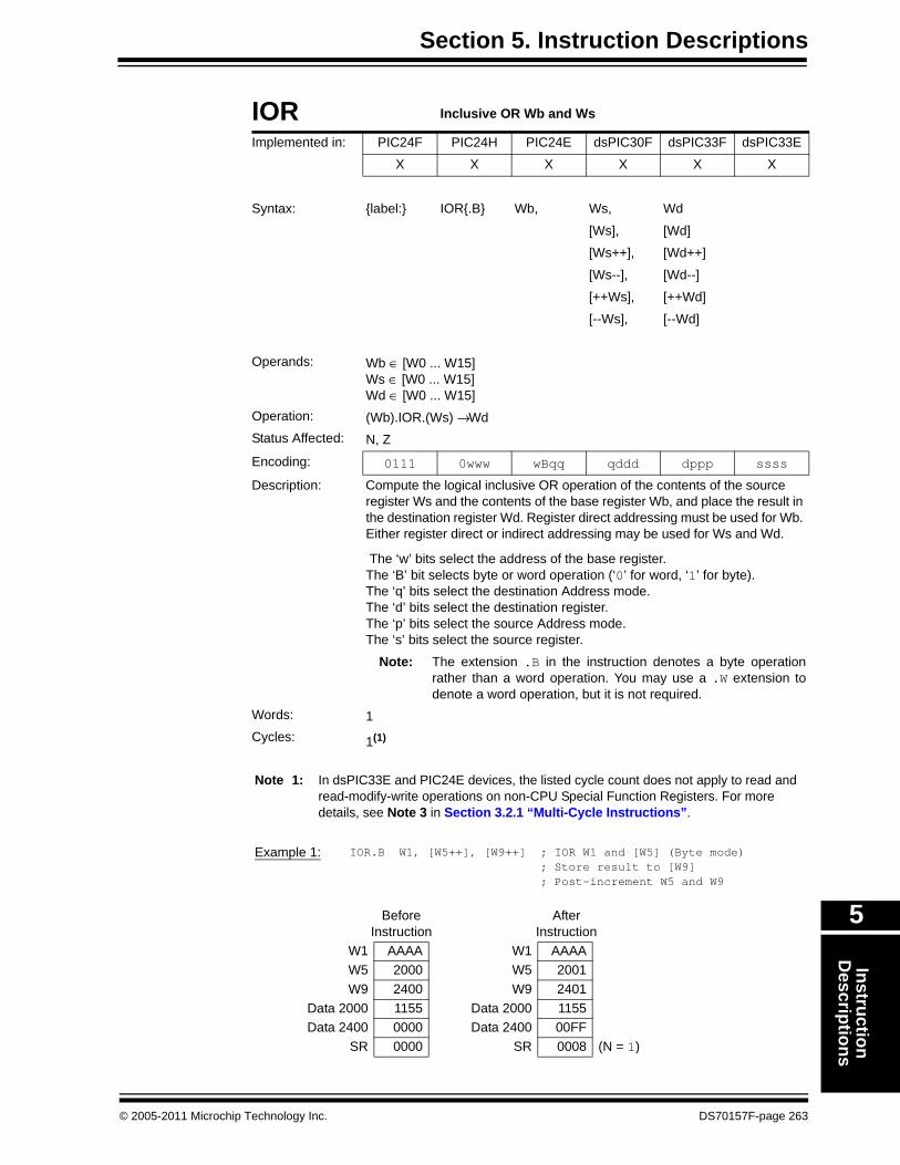
Section 5. Instruction DescriptionsInstruction
Descriptions
5
IOR Inclusive OR Wb and Ws
Implemented in: PIC24F PIC24H PIC24E dsPIC30F dsPIC33F dsPIC33E
X X X X X X
Syntax: {label:} IOR{.B} Wb, Ws, Wd
[Ws], [Wd]
[Ws++], [Wd++]
[Ws--], [Wd--]
[++Ws], [++Wd]
[--Ws], [--Wd]
Operands: Wb ∈ [W0 ... W15]Ws ∈ [W0 ... W15]Wd ∈ [W0 ... W15]
Operation: (Wb).IOR.(Ws) → Wd Status Affected: N, Z
Encoding: 0111 0www wBqq qddd dppp ssss
Description: Compute the logical inclusive OR operation of the contents of the source register Ws and the contents of the base register Wb, and place the result in the destination register Wd. Register direct addressing must be used for Wb. Either register direct or indirect addressing may be used for Ws and Wd.
The ‘w’ bits select the address of the base register.The ‘B’ bit selects byte or word operation (‘0’ for word, ‘1’ for byte).The ‘q’ bits select the destination Address mode.The ‘d’ bits select the destination register.The ‘p’ bits select the source Address mode.The ‘s’ bits select the source register.
Note: The extension .B in the instruction denotes a byte operation rather than a word operation. You may use a .W extension to denote a word operation, but it is not required.
Words: 1Cycles: 1(1)
Note 1: In dsPIC33E and PIC24E devices, the listed cycle count does not apply to read and read-modify-write operations on non-CPU Special Function Registers. For more details, see Note 3 in Section 3.2.1 “Multi-Cycle Instructions”.
Example 1: IOR.B W1, [W5++], [W9++] ; IOR W1 and [W5] (Byte mode) ; Store result to [W9] ; Post-increment W5 and W9
Before Instruction
After Instruction
W1 AAAA W1 AAAAW5 2000 W5 2001W9 2400 W9 2401
Data 2000 1155 Data 2000 1155Data 2400 0000 Data 2400 00FF
SR 0000 SR 0008 (N = 1)
© 2005-2011 Microchip Technology Inc. DS70157F-page 263
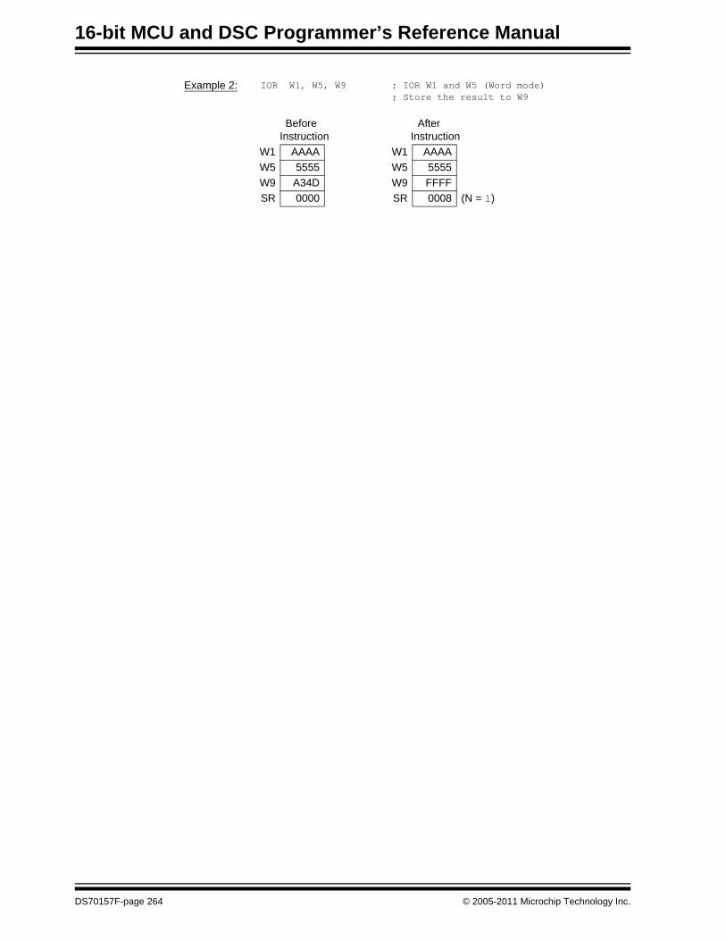
16-bit MCU and DSC Programmer’s Reference Manual
Example 2: IOR W1, W5, W9 ; IOR W1 and W5 (Word mode) ; Store the result to W9
Before Instruction
After Instruction
W1 AAAA W1 AAAAW5 5555 W5 5555W9 A34D W9 FFFFSR 0000 SR 0008 (N = 1)
DS70157F-page 264 © 2005-2011 Microchip Technology Inc.

Section 5. Instruction DescriptionsInstruction
Descriptions
5
LAC Load Accumulator
Implemented in: PIC24F PIC24H PIC24E dsPIC30F dsPIC33F dsPIC33E
X X X
Syntax: {label:} LAC Ws, {#Slit4,} Acc
[Ws],
[Ws++],
[Ws--],
[--Ws],
[++Ws],
[Ws+Wb],
Operands: Ws ∈ [W0 ... W15]Wb ∈ [W0 ... W15]Slit4 ∈ [-8 ... +7]Acc ∈ [A,B]
Operation: ShiftSlit4(Extend(Ws)) → Acc(A or B)
Status Affected: OA, OB, OAB, SA, SB, SAB
Encoding: 1100 1010 Awww wrrr rggg ssss
Description: Read the contents of the source register, optionally perform a signed 4-bit shift and store the result in the specified accumulator. The shift range is -8:7, where a negative operand indicates an arithmetic left shift and a positive operand indicates an arithmetic right shift. The data stored in the source register is assumed to be 1.15 fractional data and is automatically sign-extended (through bit 39) and zero-backfilled (bits [15:0]), prior to shifting.
The ‘A’ bit specifies the destination accumulator.The ‘w’ bits specify the offset register Wb.The ‘r’ bits encode the accumulator pre-shift.The ‘g’ bits select the source Address mode.The ‘s’ bits specify the source register Ws.
Note: If the operation moves more than sign-extension data into the upper Accumulator register (AccxU), or causes a saturation, the appropriate overflow and saturation bits will be set.
Words: 1Cycles: 1(1)
Note 1: In dsPIC33E and PIC24E devices, the listed cycle count does not apply to read and read-modify-write operations on non-CPU Special Function Registers. For more details, see Note 3 in Section 3.2.1 “Multi-Cycle Instructions”.
© 2005-2011 Microchip Technology Inc. DS70157F-page 265
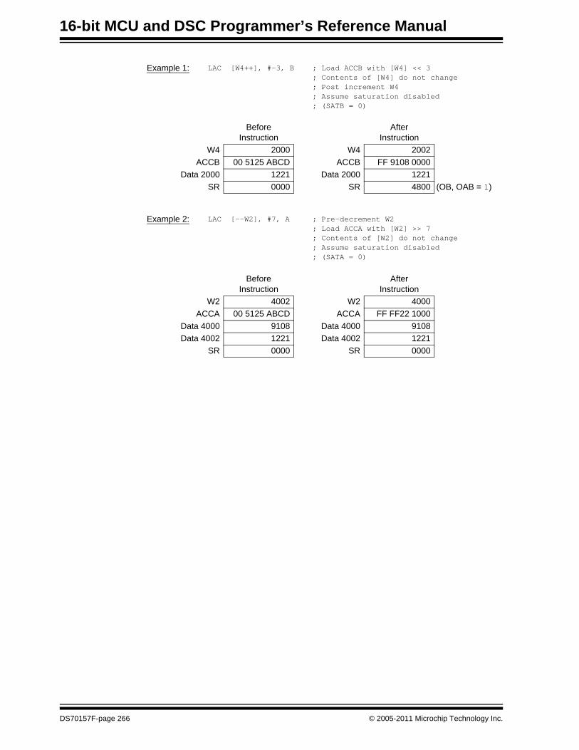
16-bit MCU and DSC Programmer’s Reference Manual
Example 1: LAC [W4++], #-3, B ; Load ACCB with [W4] << 3 ; Contents of [W4] do not change ; Post increment W4 ; Assume saturation disabled ; (SATB = 0)
Before Instruction
After Instruction
W4 2000 W4 2002ACCB 00 5125 ABCD ACCB FF 9108 0000
Data 2000 1221 Data 2000 1221SR 0000 SR 4800 (OB, OAB = 1)
Example 2: LAC [--W2], #7, A ; Pre-decrement W2 ; Load ACCA with [W2] >> 7 ; Contents of [W2] do not change ; Assume saturation disabled ; (SATA = 0)
Before Instruction
After Instruction
W2 4002 W2 4000ACCA 00 5125 ABCD ACCA FF FF22 1000
Data 4000 9108 Data 4000 9108Data 4002 1221 Data 4002 1221
SR 0000 SR 0000
DS70157F-page 266 © 2005-2011 Microchip Technology Inc.

Section 5. Instruction DescriptionsInstruction
Descriptions
5
LNK Allocate Stack Frame
Implemented in: PIC24F PIC24H PIC24E dsPIC30F dsPIC33F dsPIC33E
X X X X
Syntax: {label:} LNK #lit14
Operands: lit14 ∈ [0 ... 16382]
Operation: (W14) → (TOS)(W15) + 2 → W15(W15) → W14(W15) + lit14 → W15
Status Affected: None
Encoding: 1111 1010 00kk kkkk kkkk kkk0
Description: This instruction allocates a Stack Frame of size lit14 bytes for a subroutine calling sequence. The Stack Frame is allocated by PUSHing the contents of the Frame Pointer (W14) onto the stack, storing the updated Stack Pointer (W15) to the Frame Pointer and then incrementing the Stack Pointer by the unsigned 14-bit literal operand. This instruction supports a maximum Stack Frame of 16382 bytes.
The ‘k’ bits specify the size of the Stack Frame.
Note: Since the Stack Pointer can only reside on a word boundary, lit14 must be even.
Words: 1
Cycles: 1
Example 1: LNK #0xA0 ; Allocate a stack frame of 160 bytes
Before Instruction
After Instruction
W14 2000 W14 2002W15 2000 W15 20A2
Data 2000 0000 Data 2000 2000SR 0000 SR 0000
© 2005-2011 Microchip Technology Inc. DS70157F-page 267
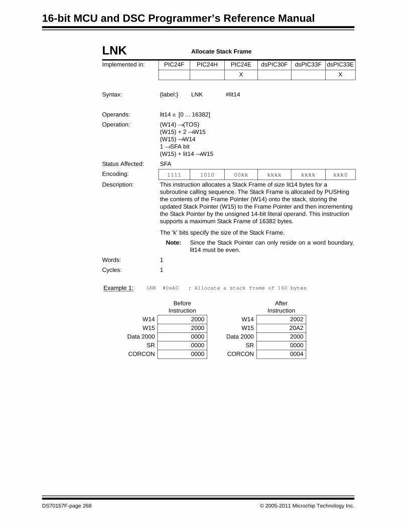
16-bit MCU and DSC Programmer’s Reference Manual
LNK Allocate Stack Frame
Implemented in: PIC24F PIC24H PIC24E dsPIC30F dsPIC33F dsPIC33E
X X
Syntax: {label:} LNK #lit14
Operands: lit14 ∈ [0 ... 16382]
Operation: (W14) → (TOS)(W15) + 2 → W15(W15) → W141 → SFA bit(W15) + lit14 → W15
Status Affected: SFA
Encoding: 1111 1010 00kk kkkk kkkk kkk0
Description: This instruction allocates a Stack Frame of size lit14 bytes for a subroutine calling sequence. The Stack Frame is allocated by PUSHing the contents of the Frame Pointer (W14) onto the stack, storing the updated Stack Pointer (W15) to the Frame Pointer and then incrementing the Stack Pointer by the unsigned 14-bit literal operand. This instruction supports a maximum Stack Frame of 16382 bytes.
The ‘k’ bits specify the size of the Stack Frame.
Note: Since the Stack Pointer can only reside on a word boundary, lit14 must be even.
Words: 1
Cycles: 1
Example 1: LNK #0xA0 ; Allocate a stack frame of 160 bytes
Before Instruction
After Instruction
W14 2000 W14 2002W15 2000 W15 20A2
Data 2000 0000 Data 2000 2000SR 0000 SR 0000
CORCON 0000 CORCON 0004
DS70157F-page 268 © 2005-2011 Microchip Technology Inc.

Section 5. Instruction DescriptionsInstruction
Descriptions
5
LSR Logical Shift Right f
Implemented in: PIC24F PIC24H PIC24E dsPIC30F dsPIC33F dsPIC33EX X X X X X
Syntax: {label:} LSR{.B} f {,WREG}
Operands: f ∈ [0 ... 8191]Operation: For byte operation:
0 → Dest<7> (f<7:1>) → Dest<6:0> (f<0>) → CFor word operation: 0 → Dest<15> (f<15:1>) → Dest<14:0> (f<0>) → C
Status Affected: N, Z, CEncoding: 1101 0101 0BDf ffff ffff ffff
Description: Shift the contents of the file register one bit to the right and place the result in the destination register. The Least Significant bit of the file register is shifted into the Carry bit of the STATUS register. Zero is shifted into the Most Significant bit of the destination register.
The optional WREG operand determines the destination register. If WREG is specified, the result is stored in WREG. If WREG is not specified, the result is stored in the file register.
The ‘B’ bit selects byte or word operation (‘0’ for word, ‘1’ for byte).The ‘D’ bit selects the destination (‘0’ for WREG, ‘1’ for file register).The ‘f’ bits select the address of the file register.Note 1: The extension .B in the instruction denotes a byte operation
rather than a word operation. You may use a .W extension to denote a word operation, but it is not required.
2: The WREG is set to working register W0. Words: 1Cycles: 1(1)
Note 1: In dsPIC33E and PIC24E devices, the listed cycle count does not apply to read and read-modify-write operations on non-CPU Special Function Registers. For more details, see Note 3 in Section 3.2.1 “Multi-Cycle Instructions”.
C0
Example 1: LSR.B 0x600 ; Logically shift right (0x600) by one ; (Byte mode)
BeforeInstruction
AfterInstruction
Data 600 55FF Data 600 557FSR 0000 SR 0001 (C = 1)
© 2005-2011 Microchip Technology Inc. DS70157F-page 269

16-bit MCU and DSC Programmer’s Reference Manual
Example 2: LSR 0x600, WREG ; Logically shift right (0x600) by one ; Store to WREG ; (Word mode)
BeforeInstruction
AfterInstruction
Data 600 55FF Data 600 55FFWREG 0000 WREG 2AFF
SR 0000 SR 0001 (C = 1)
DS70157F-page 270 © 2005-2011 Microchip Technology Inc.

Section 5. Instruction DescriptionsInstruction
Descriptions
5
LSR Logical Shift Right Ws
Implemented in: PIC24F PIC24H PIC24E dsPIC30F dsPIC33F dsPIC33E
X X X X X X
Syntax: {label:} LSR{.B} Ws, Wd
[Ws], [Wd]
[Ws++], [Wd++]
[Ws--], [Wd--]
[++Ws], [++Wd]
[--Ws], [--Wd]
Operands: Ws ∈ [W0 ... W15]Wd ∈ [W0 ... W15]
Operation: For byte operation: 0 → Wd<7> (Ws<7:1>) → Wd<6:0> (Ws<0>) → C For word operation: 0 → Wd<15> (Ws<15:1>) → Wd<14:0> (Ws<0>) → C
Status Affected: N, Z, C
Encoding: 1101 0001 0Bqq qddd dppp ssss
Description: Shift the contents of the source register Ws one bit to the right, and place the result in the destination register Wd. The Least Significant bit of Ws is shifted into the Carry bit of the STATUS register. Zero is shifted into the Most Significant bit of Wd. Either register direct or indirect addressing may be used for Ws and Wd.
The ‘B’ bit selects byte or word operation (‘0’ for word, ‘1’ for byte).The ‘q’ bits select the destination Address mode.The ‘d’ bits select the destination register.The ‘p’ bits select the source Address mode.The ‘s’ bits select the source register.
Note: The extension .B in the instruction denotes a byte operation rather than a word operation. You may use a .W extension to denote a word operation, but it is not required.
Words: 1
Cycles: 1(1)
Note 1: In dsPIC33E and PIC24E devices, the listed cycle count does not apply to read and read-modify-write operations on non-CPU Special Function Registers. For more details, see Note 3 in Section 3.2.1 “Multi-Cycle Instructions”.
C0
© 2005-2011 Microchip Technology Inc. DS70157F-page 271

16-bit MCU and DSC Programmer’s Reference Manual
Example 1: LSR.B W0, W1 ; LSR W0 (Byte mode) ; Store result to W1
Before Instruction
After Instruction
W0 FF03 W0 FF03W1 2378 W1 2301SR 0000 SR 0001 (C = 1)
Example 2: LSR W0, W1 ; LSR W0 (Word mode) ; Store the result to W1
Before Instruction
After Instruction
W0 8000 W0 8000W1 2378 W1 4000SR 0000 SR 0000
DS70157F-page 272 © 2005-2011 Microchip Technology Inc.

Section 5. Instruction DescriptionsInstruction
Descriptions
5
LSR Logical Shift Right by Short Literal
Implemented in: PIC24F PIC24H PIC24E dsPIC30F dsPIC33F dsPIC33E
X X X X X X
Syntax: {label:} LSR Wb, #lit4, Wnd
Operands: Wb ∈ [W0 ... W15]lit4 ∈ [0 ... 15]Wnd ∈ [W0 ... W15]
Operation: lit4<3:0> → Shift_Val0 → Wnd<15:15-Shift_Val + 1>Wb<15:Shift_Val> → Wnd<15-Shift_Val:0>
Status Affected: N, Z
Encoding: 1101 1110 0www wddd d100 kkkk
Description: Logical shift right the contents of the source register Wb by the 4-bit unsigned literal and store the result in the destination register Wnd. Direct addressing must be used for Wb and Wnd.
The ‘w’ bits select the address of the base register.The ‘d’ bits select the destination register.The ‘k’ bits provide the literal operand.
Note: This instruction operates in Word mode only.
Words: 1
Cycles: 1
Example 1: LSR W4, #14, W5 ; LSR W4 by 14 ; Store result to W5
Before Instruction
After Instruction
W4 C800 W4 C800W5 1200 W5 0003SR 0000 SR 0000
Example 2: LSR W4, #1, W5 ; LSR W4 by 1 ; Store result to W5
Before Instruction
After Instruction
W4 0505 W4 0505W5 F000 W5 0282SR 0000 SR 0000
© 2005-2011 Microchip Technology Inc. DS70157F-page 273

16-bit MCU and DSC Programmer’s Reference Manual
LSR Logical Shift Right by Wns
Implemented in: PIC24F PIC24H PIC24E dsPIC30F dsPIC33F dsPIC33E
X X X X X X
Syntax: {label:} LSR Wb, Wns, Wnd
Operands: Wb ∈ [W0 ... W15]Wns ∈ [W0 ...W15]Wnd ∈ [W0 ... W15]
Operation: Wns<4:0> → Shift_Val0 → Wnd<15:15-Shift_Val + 1>Wb<15:Shift_Val> → Wnd<15 - Shift_Val:0>
Status Affected: N, Z
Encoding: 1101 1110 0www wddd d000 ssss
Description: Logical shift right the contents of the source register Wb by the 5 Least Significant bits of Wns (only up to 15 positions) and store the result in the destination register Wnd. Direct addressing must be used for Wb and Wnd.
The ‘w’ bits select the address of the base register.The ‘d’ bits select the destination register.The ‘s’ bits select the source register.
Note 1: This instruction operates in Word mode only.2: If Wns is greater than 15, Wnd will be loaded with 0x0.
Words: 1
Cycles: 1
Example 1: LSR W0, W1, W2 ; LSR W0 by W1 ; Store result to W2
Before Instruction
After Instruction
W0 C00C W0 C00CW1 0001 W1 0001W2 2390 W2 6006SR 0000 SR 0000
Example 2: LSR W5, W4, W3 ; LSR W5 by W4 ; Store result to W3
Before Instruction
After Instruction
W3 DD43 W3 0000W4 000C W4 000CW5 0800 W5 0800SR 0000 SR 0002 (Z = 1)
DS70157F-page 274 © 2005-2011 Microchip Technology Inc.

Section 5. Instruction DescriptionsInstruction
Descriptions
5
MAC Multiply and Accumulate
Implemented in: PIC24F PIC24H PIC24E dsPIC30F dsPIC33F dsPIC33E
X X X
Syntax: {label:} MAC Wm*Wn, Acc {,[Wx], Wxd} {,[Wy], Wyd} {,AWB}
{,[Wx] + = kx, Wxd} {,[Wy] + = ky, Wyd}
{,[Wx] – = kx, Wxd} {,[Wy] – = ky, Wyd}
{,[W9 + W12], Wxd} {,[W11 + W12], Wyd}
Operands: Wm * Wn ∈ [W4 * W5, W4 * W6, W4 * W7, W5 * W6, W5 * W7, W6 * W7]Acc ∈ [A,B]Wx ∈ [W8, W9]; kx ∈ [-6, -4, -2, 2, 4, 6]; Wxd ∈ [W4 ... W7]Wy ∈ [W10, W11]; ky ∈ [-6, -4, -2, 2, 4, 6]; Wyd ∈ [W4 ... W7]AWB ∈ [W13, [W13] + = 2]
Operation: (Acc(A or B)) + (Wm) * (Wn) → Acc(A or B)([Wx]) → Wxd; (Wx) + kx → Wx([Wy]) → Wyd; (Wy) + ky → Wy(Acc(B or A)) rounded → AWB
Status Affected: OA, OB, OAB, SA, SB, SAB
Encoding: 1100 0mmm A0xx yyii iijj jjaa
Description: Multiply the contents of two working registers, optionally prefetch operands in preparation for another MAC type instruction and optionally store the unspecified accumulator results. The 32-bit result of the signed multiply is sign-extended to 40 bits and added to the specified accumulator.
Operands Wx, Wxd, Wy and Wyd specify optional prefetch operations, which support indirect and register offset addressing, as described in Section 4.14.1 “MAC Prefetches”. Operand AWB specifies the optional store of the “other” accumulator, as described in Section 4.14.4 “MAC Write Back”.
The ‘m’ bits select the operand registers Wm and Wn for the multiply.The ‘A’ bit selects the accumulator for the result. The ‘x’ bits select the prefetch Wxd destination.The ‘y’ bits select the prefetch Wyd destination.The ‘i’ bits select the Wx prefetch operation.The ‘j’ bits select the Wy prefetch operation.The ‘a’ bits select the accumulator Write Back destination.Note 1: The IF bit (CORCON<0>), determines if the multiply is
fractional or an integer.2: The US<1:0> bits (CORCON<13:12> in dsPIC33E, COR-
CON<12> in dsPIC30F/dsPIC33F) determine if the multiply is unsigned, signed, or mixed-sign. Only dsPIC33E devices support mixed-sign multiplication.
Words: 1
Cycles: 1
© 2005-2011 Microchip Technology Inc. DS70157F-page 275
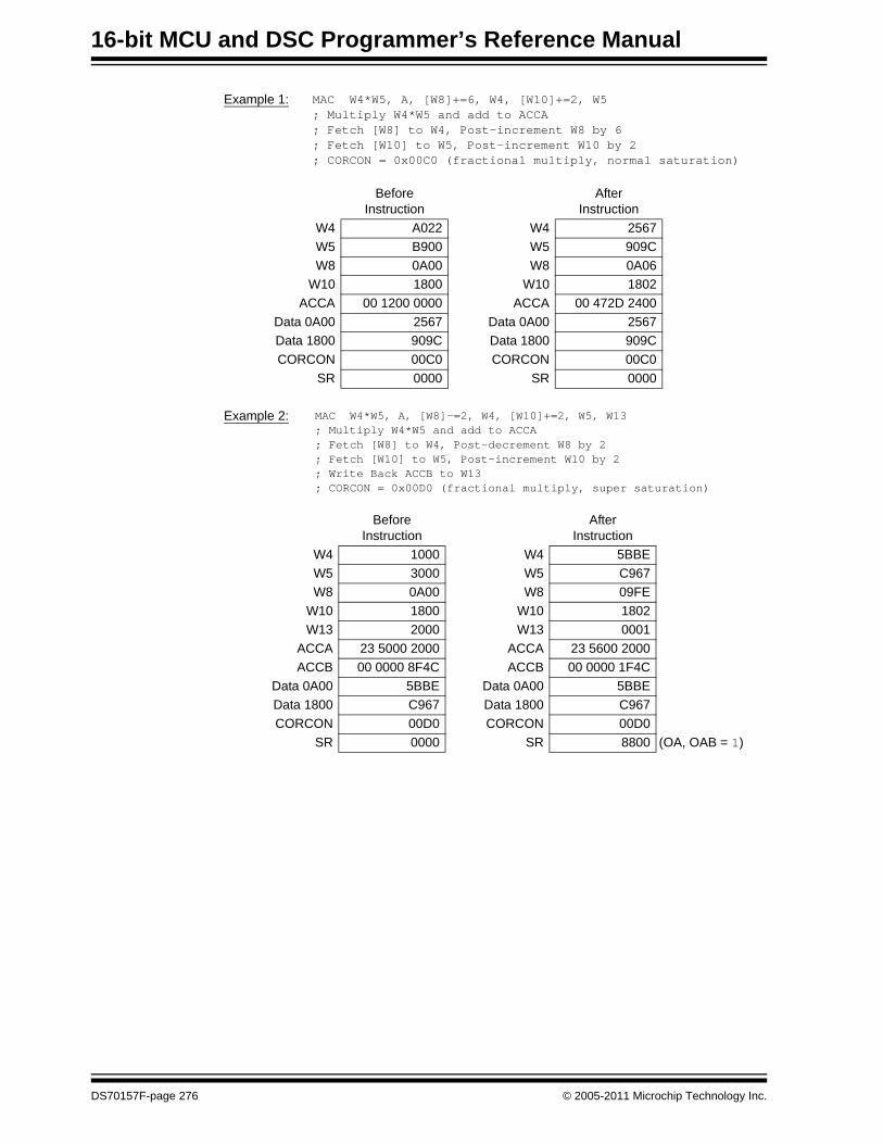
16-bit MCU and DSC Programmer’s Reference Manual
Example 1: MAC W4*W5, A, [W8]+=6, W4, [W10]+=2, W5 ; Multiply W4*W5 and add to ACCA ; Fetch [W8] to W4, Post-increment W8 by 6; Fetch [W10] to W5, Post-increment W10 by 2; CORCON = 0x00C0 (fractional multiply, normal saturation)
Before Instruction
After Instruction
W4 A022 W4 2567W5 B900 W5 909CW8 0A00 W8 0A06
W10 1800 W10 1802ACCA 00 1200 0000 ACCA 00 472D 2400
Data 0A00 2567 Data 0A00 2567Data 1800 909C Data 1800 909CCORCON 00C0 CORCON 00C0
SR 0000 SR 0000
Example 2: MAC W4*W5, A, [W8]-=2, W4, [W10]+=2, W5, W13; Multiply W4*W5 and add to ACCA; Fetch [W8] to W4, Post-decrement W8 by 2; Fetch [W10] to W5, Post-increment W10 by 2; Write Back ACCB to W13; CORCON = 0x00D0 (fractional multiply, super saturation)
Before Instruction
After Instruction
W4 1000 W4 5BBEW5 3000 W5 C967W8 0A00 W8 09FE
W10 1800 W10 1802W13 2000 W13 0001
ACCA 23 5000 2000 ACCA 23 5600 2000ACCB 00 0000 8F4C ACCB 00 0000 1F4C
Data 0A00 5BBE Data 0A00 5BBEData 1800 C967 Data 1800 C967CORCON 00D0 CORCON 00D0
SR 0000 SR 8800 (OA, OAB = 1)
DS70157F-page 276 © 2005-2011 Microchip Technology Inc.

Section 5. Instruction DescriptionsInstruction
Descriptions
5
MAC Square and Accumulate
Implemented in: PIC24F PIC24H PIC24E dsPIC30F dsPIC33F dsPIC33E
X X X
Syntax: {label:} MAC Wm*Wm, Acc {,[Wx], Wxd} {,[Wy], Wyd}
{,[Wx] + = kx, Wxd} {,[Wy] + = ky, Wyd}
{,[Wx] – = kx, Wxd} {,[Wy] – = ky, Wyd}
{,[W9 + W12], Wxd} {,[W11 + W12], Wyd}
Operands: Wm * Wm ∈ [W4 * W4, W5 * W5, W6 * W6, W7 * W7]Acc ∈ [A,B]Wx ∈ [W8, W9]; kx ∈ [-6, -4, -2, 2, 4, 6]; Wxd ∈ [W4 ... W7]Wy ∈ [W10, W11]; ky ∈ [-6, -4, -2, 2, 4, 6]; Wyd ∈ [W4 ... W7]
Operation: (Acc(A or B)) + (Wm) * (Wm) → Acc(A or B)([Wx]) → Wxd; (Wx) + kx → Wx([Wy]) → Wyd; (Wy) + ky → Wy
Status Affected: OA, OB, OAB, SA, SB, SAB
Encoding: 1111 00mm A0xx yyii iijj jj00
Description: Square the contents of a working register, optionally prefetch operands in preparation for another MAC type instruction. The 32-bit result of the signed multiply is sign-extended to 40 bits and added to the specified accumulator.
Operands Wx, Wxd, Wy and Wyd specify optional prefetch operations, which support indirect and register offset addressing, as described in Section 4.14.1 “MAC Prefetches”.
The ‘m’ bits select the operand register Wm for the square.The ‘A’ bit selects the accumulator for the result. The ‘x’ bits select the prefetch Wxd destination.The ‘y’ bits select the prefetch Wyd destination.The ‘i’ bits select the Wx prefetch operation.The ‘j’ bits select the Wy prefetch operation.Note 1: The IF bit (CORCON<0>), determines if the multiply is frac-
tional or an integer.2: The US<1:0> bits (CORCON<13:12> in dsPIC33E,
CORCON<12> in dsPIC30F/dsPIC33F) determine if the multiply is unsigned, signed, or mixed-sign. Only dsPIC33E devices support mixed-sign multiplication.
Words: 1
Cycles: 1
© 2005-2011 Microchip Technology Inc. DS70157F-page 277

16-bit MCU and DSC Programmer’s Reference Manual
Example 1: MAC W4*W4, B, [W9+W12], W4, [W10]-=2, W5 ; Square W4 and add to ACCB; Fetch [W9+W12] to W4; Fetch [W10] to W5, Post-decrement W10 by 2; CORCON = 0x00C0 (fractional multiply, normal saturation)
Before Instruction
After Instruction
W4 A022 W4 A230W5 B200 W5 650BW9 0C00 W9 0C00
W10 1900 W10 18FEW12 0020 W12 0020
ACCB 00 2000 0000 ACCB 00 67CD 0908Data 0C20 A230 Data 0C20 A230Data 1900 650B Data 1900 650BCORCON 00C0 CORCON 00C0
SR 0000 SR 0000
Example 2: MAC W7*W7, A, [W11]-=2, W7; Square W7 and add to ACCA ; Fetch [W11] to W7, Post-decrement W11 by 2; CORCON = 0x00D0 (fractional multiply, super saturation)
Before Instruction
After Instruction
W7 76AE W7 23FFW11 2000 W11 1FFE
ACCA FE 9834 4500 ACCA FF 063E 0188Data 2000 23FF Data 2000 23FFCORCON 00D0 CORCON 00D0
SR 0000 SR 8800 (OA, OAB = 1)
DS70157F-page 278 © 2005-2011 Microchip Technology Inc.

Section 5. Instruction DescriptionsInstruction
Descriptions
5
MOV Move f to Destination
Implemented in: PIC24F PIC24H PIC24E dsPIC30F dsPIC33F dsPIC33E
X X X X X X
Syntax: {label:} MOV{.B} f {,WREG}
Operands: f ∈ [0 ... 8191]
Operation: (f) → destination designated by D
Status Affected: N, Z
Encoding: 1011 1111 1BDf ffff ffff ffff
Description: Move the contents of the specified file register to the destination register. The optional WREG operand determines the destination register. If WREG is specified, the result is stored in WREG. If WREG is not specified, the result is stored back to the file register and the only effect is to modify the STATUS register.
The ‘B’ bit selects byte or word operation (‘0’ for word, ‘1’ for byte).The ‘D’ bit selects the destination (‘0’ for WREG, ‘1’ for file register).The ‘f’ bits select the address of the file register.
Note 1: The extension .B in the instruction denotes a byte operation rather than a word operation. You may use a .W extension to denote a word operation, but it is not required.
2: The WREG is set to working register W0.3: When moving word data from file register memory, the “MOV f
to Wnd” (page 281) instruction allows any working register (W0:W15) to be the destination register.
Words: 1
Cycles: 1(1)
Note 1: In dsPIC33E and PIC24E devices, the listed cycle count does not apply to read and read-modify-write operations on non-CPU Special Function Registers. For more details, see Note 3 in Section 3.2.1 “Multi-Cycle Instructions”.
Example 1: MOV.B TMR0, WREG ; move (TMR0) to WREG (Byte mode)
Before Instruction
After Instruction
WREG (W0) 9080 WREG (W0) 9055TMR0 2355 TMR0 2355
SR 0000 SR 0000
Example 2: MOV 0x800 ; update SR based on (0x800) (Word mode)
Before Instruction
After Instruction
Data 0800 B29F Data 0800 B29FSR 0000 SR 0008 (N = 1)
© 2005-2011 Microchip Technology Inc. DS70157F-page 279
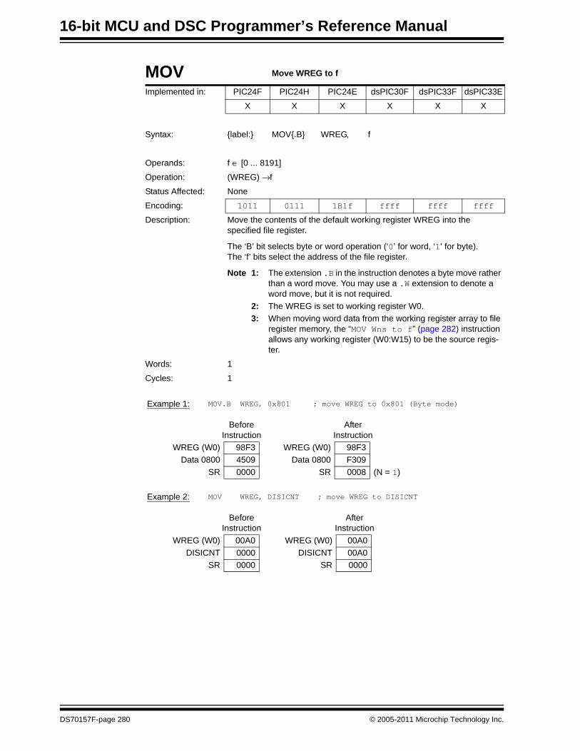
16-bit MCU and DSC Programmer’s Reference Manual
MOV Move WREG to f
Implemented in: PIC24F PIC24H PIC24E dsPIC30F dsPIC33F dsPIC33E
X X X X X X
Syntax: {label:} MOV{.B} WREG, f
Operands: f ∈ [0 ... 8191]
Operation: (WREG) → f
Status Affected: None
Encoding: 1011 0111 1B1f ffff ffff ffff
Description: Move the contents of the default working register WREG into the specified file register.
The ‘B’ bit selects byte or word operation (‘0’ for word, ‘1’ for byte).The ‘f’ bits select the address of the file register.
Note 1: The extension .B in the instruction denotes a byte move rather than a word move. You may use a .W extension to denote a word move, but it is not required.
2: The WREG is set to working register W0.3: When moving word data from the working register array to file
register memory, the “MOV Wns to f” (page 282) instruction allows any working register (W0:W15) to be the source regis-ter.
Words: 1
Cycles: 1
Example 1: MOV.B WREG, 0x801 ; move WREG to 0x801 (Byte mode)
Before Instruction
After Instruction
WREG (W0) 98F3 WREG (W0) 98F3Data 0800 4509 Data 0800 F309
SR 0000 SR 0008 (N = 1)
Example 2: MOV WREG, DISICNT ; move WREG to DISICNT
Before Instruction
After Instruction
WREG (W0) 00A0 WREG (W0) 00A0DISICNT 0000 DISICNT 00A0
SR 0000 SR 0000
DS70157F-page 280 © 2005-2011 Microchip Technology Inc.

Section 5. Instruction DescriptionsInstruction
Descriptions
5
MOV Move f to Wnd
Implemented in: PIC24F PIC24H PIC24E dsPIC30F dsPIC33F dsPIC33E
X X X X X X
Syntax: {label:} MOV f, Wnd
Operands: f ∈ [0 ... 65534]Wnd ∈ [W0 ... W15]
Operation: (f) → Wnd
Status Affected: None
Encoding: 1000 0fff ffff ffff ffff dddd
Description: Move the word contents of the specified file register to Wnd. The file register may reside anywhere in the 32K words of data memory, but must be word-aligned. Register direct addressing must be used for Wnd.
The ‘f’ bits select the address of the file register.The ‘d’ bits select the destination register.
Note 1: This instruction operates on word operands only.2: Since the file register address must be word-aligned, only the
upper 15 bits of the file register address are encoded (bit 0 is assumed to be ‘0’).
3: To move a byte of data from file register memory, the “MOV f to Destination” instruction (page 279) may be used.
Words: 1
Cycles: 1(1)
Note 1: In dsPIC33E and PIC24E devices, the listed cycle count does not apply to read and read-modify-write operations on non-CPU Special Function Registers. For more details, see Note 3 in Section 3.2.1 “Multi-Cycle Instructions”.
Example 1: MOV CORCON, W12 ; move CORCON to W12
Before Instruction
After Instruction
W12 78FA W12 00F0CORCON 00F0 CORCON 00F0
SR 0000 SR 0000
Example 2: MOV 0x27FE, W3 ; move (0x27FE) to W3
Before Instruction
After Instruction
W3 0035 W3 ABCDData 27FE ABCD Data 27FE ABCD
SR 0000 SR 0000
© 2005-2011 Microchip Technology Inc. DS70157F-page 281

16-bit MCU and DSC Programmer’s Reference Manual
MOV Move Wns to f
Implemented in: PIC24F PIC24H PIC24E dsPIC30F dsPIC33F dsPIC33E
X X X X X X
Syntax: {label:} MOV Wns, f
Operands: f ∈ [0 ... 65534]Wns ∈ [W0 ... W15]
Operation: (Wns) → f
Status Affected: None
Encoding: 1000 1fff ffff ffff ffff ssss
Description: Move the word contents of the working register Wns to the specified file register. The file register may reside anywhere in the 32K words of data memory, but must be word-aligned. Register direct addressing must be used for Wn.
The ‘f’ bits select the address of the file register.The ‘s’ bits select the source register.
Note 1: This instruction operates on word operands only.2: Since the file register address must be word-aligned, only the
upper 15 bits of the file register address are encoded (bit 0 is assumed to be ‘0’).
3: To move a byte of data to file register memory, the “MOV WREG to f” instruction (page 280) may be used.
Words: 1
Cycles: 1
Example 1: MOV W4, XMDOSRT ; move W4 to XMODSRT
Before Instruction
After Instruction
W4 1200 W4 1200XMODSRT 1340 XMODSRT 1200
SR 0000 SR 0000
Example 2: MOV W8, 0x1222 ; move W8 to data address 0x1222
Before Instruction
After Instruction
W8 F200 W8 F200Data 1222 FD88 Data 1222 F200
SR 0000 SR 0000
DS70157F-page 282 © 2005-2011 Microchip Technology Inc.

Section 5. Instruction DescriptionsInstruction
Descriptions
5
MOV.B Move 8-bit Literal to Wnd
Implemented in: PIC24F PIC24H PIC24E dsPIC30F dsPIC33F dsPIC33E
X X X X X X
Syntax: {label:} MOV.B #lit8, Wnd
Operands: lit8 ∈ [0 ... 255] Wnd ∈ [W0 ... W15]
Operation: lit8 → Wnd
Status Affected: None
Encoding: 1011 0011 1100 kkkk kkkk dddd
Description: The unsigned 8-bit literal ‘k’ is loaded into the lower byte of Wnd. The upper byte of Wnd is not changed. Register direct addressing must be used for Wnd.
The ‘k’ bits specify the value of the literal.The ‘d’ bits select the address of the working register.
Note: This instruction operates in Byte mode and the .B extension must be provided.
Words: 1
Cycles: 1
Example 1: MOV.B #0x17, W5 ; load W5 with #0x17 (Byte mode)
Before Instruction
After Instruction
W5 7899 W5 7817SR 0000 SR 0000
Example 2: MOV.B #0xFE, W9 ; load W9 with #0xFE (Byte mode)
Before Instruction
After Instruction
W9 AB23 W9 ABFESR 0000 SR 0000
© 2005-2011 Microchip Technology Inc. DS70157F-page 283

16-bit MCU and DSC Programmer’s Reference Manual
MOV Move 16-bit Literal to Wnd
Implemented in: PIC24F PIC24H PIC24E dsPIC30F dsPIC33F dsPIC33E
X X X X X X
Syntax: {label:} MOV #lit16, Wnd
Operands: lit16 ∈ [-32768 ... 65535]Wnd ∈ [W0 ... W15]
Operation: lit16 → Wnd
Status Affected: None
Encoding: 0010 kkkk kkkk kkkk kkkk dddd
Description: The 16-bit literal ‘k’ is loaded into Wnd. Register direct addressing must be used for Wnd.
The ‘k’ bits specify the value of the literal.The ‘d’ bits select the address of the working register.
Note 1: This instruction operates only in Word mode.2: The literal may be specified as a signed value [-32768:32767],
or unsigned value [0:65535].
Words: 1
Cycles: 1
Example 1: MOV #0x4231, W13 ; load W13 with #0x4231
Before Instruction
After Instruction
W13 091B W13 4231SR 0000 SR 0000
Example 2: MOV #0x4, W2 ; load W2 with #0x4
Before Instruction
After Instruction
W2 B004 W2 0004SR 0000 SR 0000
Example 3: MOV #-1000, W8 ; load W8 with #-1000
Before Instruction
After Instruction
W8 23FF W8 FC18SR 0000 SR 0000
DS70157F-page 284 © 2005-2011 Microchip Technology Inc.

Section 5. Instruction DescriptionsInstruction
Descriptions
5
MOV Move [Ws with offset] to Wnd
Implemented in: PIC24F PIC24H PIC24E dsPIC30F dsPIC33F dsPIC33E
X X X X X X
Syntax: {label:} MOV{.B} [Ws + Slit10], Wnd
Operands: Ws ∈ [W0 ... W15]Slit10 ∈ [-512 ... 511] for byte operationSlit10 ∈ [-1024 ... 1022] (even only) for word operationWnd ∈ [W0 ... W15]
Operation: [Ws + Slit10] → Wnd
Status Affected: None
Encoding: 1001 0kkk kBkk kddd dkkk ssss
Description: The contents of [Ws + Slit10] are loaded into Wnd. In Word mode, the range of Slit10 is increased to [-1024 ... 1022] and Slit10 must be even to maintain word address alignment. Register indirect addressing must be used for the source, and direct addressing must be used for Wnd.
The ‘k’ bits specify the value of the literal.The ‘B’ bit selects byte or word operation (‘0’ for word, ‘1’ for byte).The ‘d’ bits select the destination register.The ‘s’ bits select the source register.
Note 1: The extension .B in the instruction denotes a byte move rather than a word move. You may use a .W extension to denote a word move, but it is not required.
2: In Byte mode, the range of Slit10 is not reduced as specified in Section 4.6 “Using 10-bit Literal Operands”, since the literal represents an address offset from Ws.
Words: 1
Cycles: 1(1)
Note 1: In dsPIC33E and PIC24E devices, the listed cycle count does not apply to read and read-modify-write operations on non-CPU Special Function Registers. For more details, see Note 3 in Section 3.2.1 “Multi-Cycle Instructions”.
Example 1: MOV.B [W8+0x13], W10 ; load W10 with [W8+0x13] ; (Byte mode)
Before Instruction
After Instruction
W8 1008 W8 1008W10 4009 W10 4033
Data 101A 3312 Data 101A 3312SR 0000 SR 0000
© 2005-2011 Microchip Technology Inc. DS70157F-page 285

16-bit MCU and DSC Programmer’s Reference Manual
Example 2: MOV [W4+0x3E8], W2 ; load W2 with [W4+0x3E8] ; (Word mode)
Before Instruction
After Instruction
W2 9088 W2 5634W4 0800 W4 0800
Data 0BE8 5634 Data 0BE8 5634SR 0000 SR 0000
MOV Move Wns to [Wd with offset]
Implemented in: PIC24F PIC24H PIC24E dsPIC30F dsPIC33F dsPIC33E
X X X X X X
Syntax: {label:} MOV{.B} Wns, [Wd + Slit10]
Operands: Wns ∈ [W0 ... W15]Slit10 ∈ [-512 ... 511] in Byte modeSlit10 ∈ [-1024 ... 1022] (even only) in Word modeWd ∈ [W0 ... W15]
Operation: (Wns) → [Wd + Slit10]
Status Affected: None
Encoding: 1001 1kkk kBkk kddd dkkk ssss
Description: The contents of Wns are stored to [Wd + Slit10]. In Word mode, the range of Slit10 is increased to [-1024 ... 1022] and Slit10 must be even to maintain word address alignment. Register direct addressing must be used for Wns, and indirect addressing must be used for the destination.
The ‘k’ bits specify the value of the literal.The ‘B’ bit selects byte or word operation (‘0’ for word, ‘1’ for byte).The ‘d’ bits select the destination register.The ‘s’ bits select the source register.
Note 1: The extension .B in the instruction denotes a byte move rather than a word move. You may use a .W extension to denote a word move, but it is not required.
2: In Byte mode, the range of Slit10 is not reduced as specified in Section 4.6 “Using 10-bit Literal Operands”, since the literal represents an address offset from Wd.
Words: 1
Cycles: 1
Example 1: MOV.B W0, [W1+0x7] ; store W0 to [W1+0x7] ; (Byte mode)
Before Instruction
After Instruction
W0 9015 W0 9015W1 1800 W1 1800
Data 1806 2345 Data 1806 1545SR 0000 SR 0000
DS70157F-page 286 © 2005-2011 Microchip Technology Inc.

Section 5. Instruction DescriptionsInstruction
Descriptions
5
Example 2: MOV W11, [W1-0x400] ; store W11 to [W1-0x400] ; (Word mode)
Before Instruction
After Instruction
W1 1000 W1 1000W11 8813 W11 8813
Data 0C00 FFEA Data 0C00 8813SR 0000 SR 0000
MOV Move Ws to Wd
Implemented in: PIC24F PIC24H PIC24E dsPIC30F dsPIC33F dsPIC33E
X X X X X X
Syntax: {label:} MOV{.B} Ws, Wd
[Ws], [Wd]
[Ws++], [Wd++]
[Ws--], [Wd--]
[--Ws], [--Wd]
[++Ws], [++Wd]
[Ws + Wb], [Wd + Wb]
Operands: Ws ∈ [W0 ... W15]Wb ∈ [W0 ... W15]Wd ∈ [W0 ... W15]
Operation: (Ws) → Wd
Status Affected: None
Encoding: 0111 1www wBhh hddd dggg ssss
Description: Move the contents of the source register into the destination register. Either register direct or indirect addressing may be used for Ws and Wd.
The ‘w’ bits define the offset register Wb.The ‘B’ bit selects byte or word operation (‘0’ for word, ‘1’ for byte).The ‘h’ bits select the destination Address mode.The ‘d’ bits select the destination register.The ‘g’ bits select the source Address mode.The ‘s’ bits select the source register.
Note 1: The extension .B in the instruction denotes a byte move rather than a word move. You may use a .W extension to denote a word move, but it is not required.
2: When Register Offset Addressing mode is used for both the source and destination, the offset must be the same because the ‘w’ encoding bits are shared by Ws and Wd.
3: The instruction “PUSH Ws” translates to MOV Ws, [W15++].4: The instruction “POP Wd” translates to MOV [--W15], Wd.
© 2005-2011 Microchip Technology Inc. DS70157F-page 287

16-bit MCU and DSC Programmer’s Reference Manual
Words: 1
Cycles: 1(1)
Note 1: In dsPIC33E and PIC24E devices, the listed cycle count does not apply to read and read-modify-write operations on non-CPU Special Function Registers. For more details, see Note 3 in Section 3.2.1 “Multi-Cycle Instructions”.
MOV Move Ws to Wd
Example 1: MOV.B [W0--], W4 ; Move [W0] to W4 (Byte mode) ; Post-decrement W0
Before Instruction
After Instruction
W0 0A01 W0 0A00W4 2976 W4 2989
Data 0A00 8988 Data 0A00 8988SR 0000 SR 0000
Example 2: MOV [W6++], [W2+W3] ; Move [W6] to [W2+W3] (Word mode) ; Post-increment W6
Before Instruction
After Instruction
W2 0800 W2 0800W3 0040 W3 0040W6 1228 W6 122A
Data 0840 9870 Data 0840 0690Data 1228 0690 Data 1228 0690
SR 0000 SR 0000
DS70157F-page 288 © 2005-2011 Microchip Technology Inc.

Section 5. Instruction DescriptionsInstruction
Descriptions
5
MOV.D Double Word Move from Source to Wnd
Implemented in: PIC24F PIC24H PIC24E dsPIC30F dsPIC33F dsPIC33E
X X X X X X
Syntax: {label:} MOV.D Wns, Wnd
[Ws],
[Ws++],
[Ws--],
[++Ws],
[--Ws],
Operands: Wns ∈ [W0, W2, W4 ... W14]Ws ∈ [W0 ... W15]Wnd ∈ [W0, W2, W4 ... W14]
Operation: For direct addressing of source: Wns → Wnd Wns + 1 → Wnd + 1For indirect addressing of source: See Description
Status Affected: None
Encoding: 1011 1110 0000 0ddd 0ppp ssss
Description: Move the double word specified by the source to a destination working register pair (Wnd:Wnd + 1). If register direct addressing is used for the source, the contents of two successive working registers (Wns:Wns + 1) are moved to Wnd:Wnd + 1. If indirect addressing is used for the source, Ws specifies the effective address for the least significant word of the double word. Any pre/post-increment or pre/post-decrement will adjust Ws by 4 bytes to accommodate for the double word.
The ‘d’ bits select the destination register. The ‘p’ bits select the source Address mode.The ‘s’ bits select the address of the first source register.
Note 1: This instruction only operates on double words. See Figure 4-3 for information on how double words are aligned in memory.
2: Wnd must be an even working register.3: The instruction “POP.D Wnd” translates to MOV.D [--W15],
Wnd.
Words: 1
Cycles: 2(1)
Note 1: In dsPIC33E and PIC24E devices, the listed cycle count does not apply to read and read-modify-write operations on non-CPU Special Function Registers. For more details, see Note 3 in Section 3.2.1 “Multi-Cycle Instructions”.
© 2005-2011 Microchip Technology Inc. DS70157F-page 289

16-bit MCU and DSC Programmer’s Reference Manual
Example 1: MOV.D W2, W6 ; Move W2 to W6 (Double mode)
Before Instruction
After Instruction
W2 12FB W2 12FBW3 9877 W3 9877W6 9833 W6 12FBW7 FCC6 W7 9877SR 0000 SR 0000
Example 2: MOV.D [W7--], W4 ; Move [W7] to W4 (Double mode) ; Post-decrement W7
Before Instruction
After Instruction
W4 B012 W4 A319W5 FD89 W5 9927W7 0900 W7 08FC
Data 0900 A319 Data 0900 A319Data 0902 9927 Data 0902 9927
SR 0000 SR 0000
DS70157F-page 290 © 2005-2011 Microchip Technology Inc.

Section 5. Instruction DescriptionsInstruction
Descriptions
5
MOVPAG Move Literal to Page Register
Implemented in: PIC24F PIC24H PIC24E dsPIC30F dsPIC33F dsPIC33E
X X
Syntax: {label:} MOVPAG #lit10, DSRPAG
#lit9, DSWPAG
#lit8, TBLPAG
Operands: lit10 ∈ [0 ... 1023], lit9 ∈ [0 ... 511], lit8 ∈ [0 ... 255]
Operation: lit10 → DSRPAG or lit9 → DSWPAG or lit8 → TBLPAG
Status Affected: None
Encoding: 1111 1110 1100 PPkk kkkk kkkk
Description: The appropriate number of bits from the unsigned literal ‘k’ are loaded into the DSRPAG, DSWPAG, or TBLPAG register. The assembler restricts the literal to a 9-bit unsigned value when the destination is DSWPAG, and an 8-bit unsigned value when the destination is TBLPAG.
The ‘P’ bits select the destination register.The ‘k’ bits specify the value of the literal.
Note: This instruction operates in word mode only.
Words: 1
Cycles: 1
Example 1: MOVPAG #0x02, DSRPAG
Before Instruction
After Instruction
DSRPAG 0000 DSRPAG 0002
© 2005-2011 Microchip Technology Inc. DS70157F-page 291

16-bit MCU and DSC Programmer’s Reference Manual
MOVPAG Move Ws to Page Register
Implemented in: PIC24F PIC24H PIC24E dsPIC30F dsPIC33F dsPIC33E
X X
Syntax: {label:} MOVPAG Wn, DSRPAG
DSWPAG
TBLPAG
Operands: Wn ∈ [W0 ... W15]
Operation: Wn<9:0> → DSRPAG or Wn<8:0> → DSWPAG or Wn<7:0> → TBLPAG
Status Affected: None
Encoding: 1111 1110 1101 PP00 0000 ssss
Description: The appropriate number of bits from the register Ws are loaded into the DSRPAG, DSWPAG, or TBLPAG register. The assembler restricts the literal to a 9-bit unsigned value when the destination is DSWPAG, and an 8-bit unsigned value when the destination is TBLPAG.
The ‘P’ bits select the destination register.The ‘s’ bits specify the source register.
Note: This instruction operates in word mode only.
Words: 1
Cycles: 1
Example 1: MOVPAG W2, DSRPAG
Before Instruction
After Instruction
DSRPAG 0000 DSRPAG 0002W2 0002 W2 0002
DS70157F-page 292 © 2005-2011 Microchip Technology Inc.

Section 5. Instruction DescriptionsInstruction
Descriptions
5
MOVSAC Prefetch Operands and Store Accumulator
Implemented in: PIC24F PIC24H PIC24E dsPIC30F dsPIC33F dsPIC33E
X X X
Syntax: {label:} MOVSAC Acc {,[Wx], Wxd} {,[Wy], Wyd} {,AWB}
{,[Wx] + = kx, Wxd} {,[Wy] + = ky, Wyd}
{,[Wx] – = kx, Wxd} {,[Wy] – = ky, Wyd}
{,[W9 + W12], Wxd} {,[W11 + W12], Wyd}
Operands: Acc ∈ [A,B]Wx ∈ [W8, W9]; kx ∈ [-6, -4, -2, 2, 4, 6]; Wxd ∈ [W4 ... W7]Wy ∈ [W10, W11]; ky ∈ [-6, -4, -2, 2, 4, 6]; Wyd ∈ [W4 ... W7]AWB ∈ [W13, [W13] + = 2]
Operation: ([Wx]) → Wxd; (Wx) + kx → Wx([Wy]) → Wyd; (Wy) + ky → Wy(Acc(B or A)) rounded → AWB
Status Affected: None
Encoding: 1100 0111 A0xx yyii iijj jjaa
Description: Optionally prefetch operands in preparation for another MAC type instruction and optionally store the unspecified accumulator results. Even though an accumulator operation is not performed in this instruction, an accumulator must be specified to designate which accumulator to write back.
Operands Wx, Wxd, Wy and Wyd specify optional prefetch operations which support indirect and register offset addressing, as described in Section 4.14.1 “MAC Prefetches”. Operand AWB specifies the optional store of the “other” accumulator, as described in Section 4.14.4 “MAC Write Back”.
The ‘A’ bit selects the other accumulator used for write back.The ‘x’ bits select the prefetch Wxd destination.The ‘y’ bits select the prefetch Wyd destination.The ‘i’ bits select the Wx prefetch operation.The ‘j’ bits select the Wy prefetch operation.The ‘a’ bits select the accumulator Write Back destination.
Words: 1
Cycles: 1
© 2005-2011 Microchip Technology Inc. DS70157F-page 293
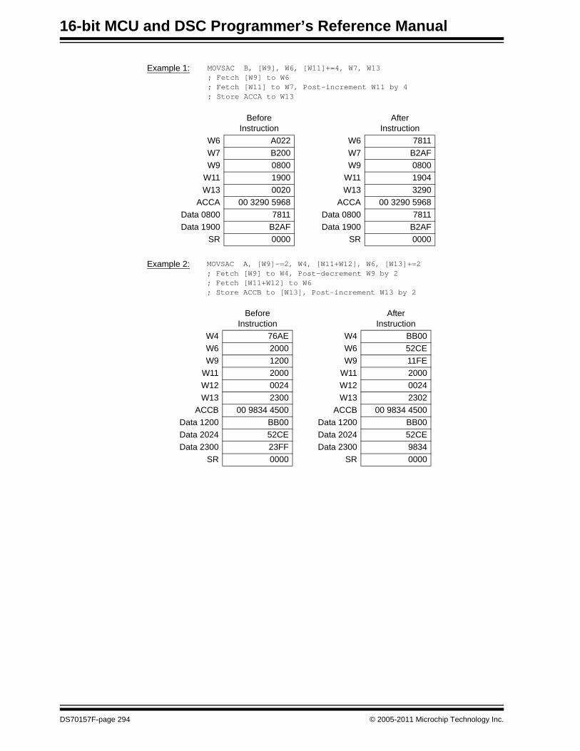
16-bit MCU and DSC Programmer’s Reference Manual
Example 1: MOVSAC B, [W9], W6, [W11]+=4, W7, W13 ; Fetch [W9] to W6 ; Fetch [W11] to W7, Post-increment W11 by 4 ; Store ACCA to W13
Before Instruction
After Instruction
W6 A022 W6 7811W7 B200 W7 B2AFW9 0800 W9 0800
W11 1900 W11 1904W13 0020 W13 3290
ACCA 00 3290 5968 ACCA 00 3290 5968Data 0800 7811 Data 0800 7811Data 1900 B2AF Data 1900 B2AF
SR 0000 SR 0000
Example 2: MOVSAC A, [W9]-=2, W4, [W11+W12], W6, [W13]+=2; Fetch [W9] to W4, Post-decrement W9 by 2; Fetch [W11+W12] to W6; Store ACCB to [W13], Post-increment W13 by 2
Before Instruction
After Instruction
W4 76AE W4 BB00W6 2000 W6 52CEW9 1200 W9 11FE
W11 2000 W11 2000W12 0024 W12 0024W13 2300 W13 2302
ACCB 00 9834 4500 ACCB 00 9834 4500Data 1200 BB00 Data 1200 BB00Data 2024 52CE Data 2024 52CEData 2300 23FF Data 2300 9834
SR 0000 SR 0000
DS70157F-page 294 © 2005-2011 Microchip Technology Inc.

Section 5. Instruction DescriptionsInstruction
Descriptions
5
MPY Multiply Wm by Wn to Accumulator
Implemented in: PIC24F PIC24H PIC24E dsPIC30F dsPIC33F dsPIC33E
X X X
Syntax: {label:} MPY Wm * Wn, Acc {,[Wx], Wxd} {,[Wy], Wyd}
{,[Wx] + = kx, Wxd} {,[Wy] + = ky, Wyd}
{,[Wx] – = kx, Wxd} {,[Wy] – = ky, Wyd}
{,[W9 + W12], Wxd} {,[W11 + W12], Wyd}
Operands: Wm * Wn ∈ [W4 * W5, W4 * W6, W4 * W7, W5 * W6, W5 * W7, W6 * W7]Acc ∈ [A,B]Wx ∈ [W8, W9]; kx ∈ [-6, -4, -2, 2, 4, 6]; Wxd ∈ [W4 ... W7]Wy ∈ [W10, W11]; ky ∈ [-6, -4, -2, 2, 4, 6]; Wyd ∈ [W4 ... W7]AWB ∈ [W13], [W13] + = 2
Operation: (Wm) * (Wn) → Acc(A or B)([Wx]) → Wxd; (Wx) + kx → Wx([Wy]) → Wyd; (Wy) + ky → Wy
Status Affected: OA, OB, OAB, SA, SB, SAB
Encoding: 1100 0mmm A0xx yyii iijj jj11
Description: Multiply the contents of two working registers, optionally prefetch operands in preparation for another MAC type instruction. The 32-bit result of the signed multiply is sign-extended to 40 bits and stored to the specified accumulator.
Operands Wx, Wxd, Wy and Wyd specify optional prefetch operations which support indirect and register offset addressing, as described in Section 4.14.1 “MAC Prefetches”.
The ‘m’ bits select the operand registers Wm and Wn for the multiply:The ‘A’ bit selects the accumulator for the result.The ‘x’ bits select the prefetch Wxd destination.The ‘y’ bits select the prefetch Wyd destination.The ‘i’ bits select the Wx prefetch operation.The ‘j’ bits select the Wy prefetch operation.Note 1: The IF bit, CORCON<0>, determines if the multiply is
fractional or an integer.2: The US<1:0> bits (CORCON<13:12> in dsPIC33E,
CORCON<12> in dsPIC30F/dsPIC33F) determine if the multiply is unsigned, signed, or mixed-sign. Only dsPIC33E devices support mixed-sign multiplication.
Words: 1
Cycles: 1
© 2005-2011 Microchip Technology Inc. DS70157F-page 295

16-bit MCU and DSC Programmer’s Reference Manual
Example 1: MPY W4*W5, A, [W8]+=2, W6, [W10]-=2, W7 ; Multiply W4*W5 and store to ACCA ; Fetch [W8] to W6, Post-increment W8 by 2 ; Fetch [W10] to W7, Post-decrement W10 by 2 ; CORCON = 0x0000 (fractional multiply, no saturation)
Before Instruction
After Instruction
W4 C000 W4 C000W5 9000 W5 9000W6 0800 W6 671FW7 B200 W7 E3DCW8 1780 W8 1782
W10 2400 W10 23FEACCA FF F780 2087 ACCA 00 3800 0000
Data 1780 671F Data 1780 671FData 2400 E3DC Data 2400 E3DCCORCON 0000 CORCON 0000
SR 0000 SR 0000
Example 2: MPY W6*W7, B, [W8]+=2, W4, [W10]-=2, W5; Multiply W6*W7 and store to ACCB; Fetch [W8] to W4, Post-increment W8 by 2 ; Fetch [W10] to W5, Post-decrement W10 by 2; CORCON = 0x0000 (fractional multiply, no saturation)
Before Instruction
After Instruction
W4 C000 W4 8FDCW5 9000 W5 0078W6 671F W6 671FW7 E3DC W7 E3DCW8 1782 W8 1784
W10 23FE W10 23FCACCB 00 9834 4500 ACCB FF E954 3748
Data 1782 8FDC Data 1782 8FDCData 23FE 0078 Data 23FE 0078CORCON 0000 CORCON 0000
SR 0000 SR 0000
DS70157F-page 296 © 2005-2011 Microchip Technology Inc.

Section 5. Instruction DescriptionsInstruction
Descriptions
5
MPY Square to Accumulator
Implemented in: PIC24F PIC24H PIC24E dsPIC30F dsPIC33F dsPIC33E
X X X
Syntax: {label:} MPY Wm * Wm, Acc {,[Wx], Wxd} {,[Wy], Wyd}
{,[Wx] + = kx, Wxd} {,[Wy] + = ky, Wyd}
{,[Wx] – = kx, Wxd} {,[Wy] – = ky, Wyd}
{,[W9 + W12], Wxd} {,[W11 + W12], Wyd}
Operands: Wm * Wm ∈ [W4 * W4, W5 * W5, W6 * W6, W7 * W7]Acc ∈ [A,B]Wx ∈ [W8, W9]; kx ∈ [-6, -4, -2, 2, 4, 6]; Wxd ∈ [W4 ... W7]Wy ∈ [W10, W11]; ky ∈ [-6, -4, -2, 2, 4, 6]; Wyd ∈ [W4 ... W7]
Operation: (Wm) * (Wm) → Acc(A or B)([Wx]) → Wxd; (Wx) + kx → Wx([Wy]) → Wyd; (Wy) + ky → Wy
Status Affected: OA, OB, OAB, SA, SB, SAB
Encoding: 1111 00mm A0xx yyii iijj jj01
Description: Square the contents of a working register, optionally prefetch operands in preparation for another MAC type instruction. The 32-bit result of the signed multiply is sign-extended to 40 bits and stored in the specified accumulator.
Operands Wx, Wxd, Wy and Wyd specify optional prefetch operations which support indirect and register offset addressing, as described in Section 4.14.1 “MAC Prefetches”.
The ‘m’ bits select the operand register Wm for the square.The ‘A’ bit selects the accumulator for the result.The ‘x’ bits select the prefetch Wxd destination.The ‘y’ bits select the prefetch Wyd destination.The ‘i’ bits select the Wx prefetch operation.The ‘j’ bits select the Wy prefetch operation.Note 1: The IF bit (CORCON<0>), determines if the multiply is
fractional or an integer.2: The US<1:0> bits (CORCON<13:12> in dsPIC33E,
CORCON<12> in dsPIC30F/dsPIC33F) determine if the multiply is unsigned, signed, or mixed-sign. Only dsPIC33E devices support mixed-sign multiplication.
Words: 1
Cycles: 1
© 2005-2011 Microchip Technology Inc. DS70157F-page 297

16-bit MCU and DSC Programmer’s Reference Manual
Example 1: MPY W6*W6, A, [W9]+=2, W6 ; Square W6 and store to ACCA ; Fetch [W9] to W6, Post-increment W9 by 2 ; CORCON = 0x0000 (fractional multiply, no saturation)
Before Instruction
After Instruction
W6 6500 W6 B865W9 0900 W9 0902
ACCA 00 7C80 0908 ACCA 00 4FB2 0000Data 0900 B865 Data 0900 B865CORCON 0000 CORCON 0000
SR 0000 SR 0000
Example 2: MPY W4*W4, B, [W9+W12], W4, [W10]+=2, W5; Square W4 and store to ACCB; Fetch [W9+W12] to W4; Fetch [W10] to W5, Post-increment W10 by 2; CORCON = 0x0000 (fractional multiply, no saturation)
Before Instruction
After Instruction
W4 E228 W4 8911 W5 9000 W5 F678W9 1700 W9 1700
W10 1B00 W10 1B02W12 FF00 W12 FF00
ACCB 00 9834 4500 ACCB 00 06F5 4C80Data 1600 8911 Data 1600 8911Data 1B00 F678 Data 1B00 F678CORCON 0000 CORCON 0000
SR 0000 SR 0000
DS70157F-page 298 © 2005-2011 Microchip Technology Inc.

Section 5. Instruction DescriptionsInstruction
Descriptions
5
MPY.N Multiply -Wm by Wn to Accumulator
Implemented in: PIC24F PIC24H PIC24E dsPIC30F dsPIC33F dsPIC33E
X X X
Syntax: {label:} MPY.N Wm * Wn, Acc {,[Wx], Wxd} {,[Wy], Wyd}
{,[Wx] + = kx, Wxd} {,[Wy] + = ky, Wyd}
{,[Wx] – = kx, Wxd} {,[Wy] – = ky, Wyd}
{,[W9 + W12], Wxd} {,[W11 + W12], Wyd}
Operands: Wm * Wn ∈ [W4 * W5; W4 * W6; W4 * W7; W5 * W6; W5 * W7; W6 * W7]Acc ∈ [A,B]Wx ∈ [W8, W9]; kx ∈ [-6, -4, -2, 2, 4, 6]; Wxd ∈ [W4 ... W7]Wy ∈ [W10, W11]; ky ∈ [-6, -4, -2, 2, 4, 6]; Wyd ∈ [W4 ... W7]
Operation: -(Wm) * (Wn) → Acc(A or B)([Wx]) → Wxd; (Wx) + kx → Wx([Wy]) → Wyd; (Wy) + ky → Wy
Status Affected: OA, OB, OAB
Encoding: 1100 0mmm A1xx yyii iijj jj11
Description: Multiply the contents of a working register by the negative of the contents of another working register, optionally prefetch operands in preparation for another MAC type instruction and optionally store the unspecified accumulator results. The 32-bit result of the signed multiply is sign-extended to 40 bits and stored to the specified accumulator.
The ‘m’ bits select the operand registers Wm and Wn for the multiply.The ‘A’ bit selects the accumulator for the result.The ‘x’ bits select the prefetch Wxd destination.The ‘y’ bits select the prefetch Wyd destination.The ‘i’ bits select the Wx prefetch operation.The ‘j’ bits select the Wy prefetch operation.Note 1: The IF bit (CORCON<0>), determines if the multiply is
fractional or an integer.2: The US<1:0> bits (CORCON<13:12> in dsPIC33E,
CORCON<12> in dsPIC30F/dsPIC33F) determine if the multiply is unsigned, signed, or mixed-sign. Only dsPIC33E devices support mixed-sign multiplication.
Words: 1
Cycles: 1
© 2005-2011 Microchip Technology Inc. DS70157F-page 299

16-bit MCU and DSC Programmer’s Reference Manual
Example 1: MPY.N W4*W5, A, [W8]+=2, W4, [W10]+=2, W5 ; Multiply W4*W5, negate the result and store to ACCA ; Fetch [W8] to W4, Post-increment W8 by 2 ; Fetch [W10] to W5, Post-increment W10 by 2 ; CORCON = 0x0001 (integer multiply, no saturation)
Before Instruction
After Instruction
W4 3023 W4 0054W5 1290 W5 660AW8 0B00 W8 0B02
W10 2000 W10 2002ACCA 00 0000 2387 ACCA FF FC82 7650
Data 0B00 0054 Data 0B00 0054Data 2000 660A Data 2000 660ACORCON 0001 CORCON 0001
SR 0000 SR 0000
Example 2: MPY.N W4*W5, A, [W8]+=2, W4, [W10]+=2, W5 ; Multiply W4*W5, negate the result and store to ACCA ; Fetch [W8] to W4, Post-increment W8 by 2 ; Fetch [W10] to W5, Post-increment W10 by 2 ; CORCON = 0x0000 (fractional multiply, no saturation)
Before Instruction
After Instruction
W4 3023 W4 0054W5 1290 W5 660AW8 0B00 W8 0B02
W10 2000 W10 2002ACCA 00 0000 2387 ACCA FF F904 ECA0
Data 0B00 0054 Data 0B00 0054Data 2000 660A Data 2000 660ACORCON 0000 CORCON 0000
SR 0000 SR 0000
DS70157F-page 300 © 2005-2011 Microchip Technology Inc.

Section 5. Instruction DescriptionsInstruction
Descriptions
5
MSC Multiply and Subtract from Accumulator
Implemented in: PIC24F PIC24H PIC24E dsPIC30F dsPIC33F dsPIC33E
X X X
Syntax: {label:} MSC Wm * Wn, Acc {,[Wx], Wxd} {,[Wy], Wyd} {,AWB}
{,[Wx] + = kx, Wxd} {,[Wy] + = ky, Wyd}
{,[Wx] – = kx, Wxd} {,[Wy] – = ky, Wyd}
{,[W9 + W12], Wxd} {,[W11 + W12], Wyd}
Operands: Wm * Wn ∈ [W4 * W5, W4 * W6, W4 * W7, W5 * W6, W5 * W7, W6 * W7]Acc ∈ [A,B]Wx ∈ [W8, W9]; kx ∈ [-6, -4, -2, 2, 4, 6]; Wxd ∈ [W4 ... W7]Wy ∈ [W10, W11]; ky ∈ [-6, -4, -2, 2, 4, 6]; Wyd ∈ [W4 ... W7]AWB ∈ [W13, [W13] + = 2]
Operation: (Acc(A or B)) − (Wm) * (Wn) → Acc(A or B)([Wx]) → Wxd; (Wx) + kx → Wx([Wy]) → Wyd; (Wy) + ky → Wy(Acc(B or A)) rounded → AWB
Status Affected: OA, OB, OAB, SA, SB, SAB
Encoding: 1100 0mmm A1xx yyii iijj jjaa
Description: Multiply the contents of two working registers, optionally prefetch operands in preparation for another MAC type instruction and optionally store the unspecified accumulator results. The 32-bit result of the signed multiply is sign-extended to 40 bits and subtracted from the specified accumulator.
Operands Wx, Wxd, Wy and Wyd specify optional prefetch operations which support indirect and register offset addressing as described in Section 4.14.1 “MAC Prefetches”. Operand AWB specifies the optional store of the “other” accumulator as described in Section 4.14.4 “MAC Write Back”.
The ‘m’ bits select the operand registers Wm and Wn for the multiply.The ‘A’ bit selects the accumulator for the result.The ‘x’ bits select the prefetch Wxd destination.The ‘y’ bits select the prefetch Wyd destination.The ‘i’ bits select the Wx prefetch operation.The ‘j’ bits select the Wy prefetch operation.The ‘a’ bits select the accumulator Write Back destination.
Note: The IF bit (CORCON<0>), determines if the multiply is fractional or an integer.
Words: 1
Cycles: 1
© 2005-2011 Microchip Technology Inc. DS70157F-page 301

16-bit MCU and DSC Programmer’s Reference Manual
Example 1: MSC W6*W7, A, [W8]-=4, W6, [W10]-=4, W7 ; Multiply W6*W7 and subtract the result from ACCA ; Fetch [W8] to W6, Post-decrement W8 by 4 ; Fetch [W10] to W7, Post-decrement W10 by 4 ; CORCON = 0x0001 (integer multiply, no saturation)
Before Instruction
After Instruction
W6 9051 W6 D309W7 7230 W7 100BW8 0C00 W8 0BFC
W10 1C00 W10 1BFCACCA 00 0567 8000 ACCA 00 3738 5ED0
Data 0C00 D309 Data 0C00 D309Data 1C00 100B Data 1C00 100BCORCON 0001 CORCON 0001
SR 0000 SR 0000
Example 2: MSC W4*W5, B, [W11+W12], W5, W13 ; Multiply W4*W5 and subtract the result from ACCB ; Fetch [W11+W12] to W5 ; Write Back ACCA to W13 ; CORCON = 0x0000 (fractional multiply, no saturation)
Before Instruction
After Instruction
W4 0500 W4 0500W5 2000 W5 3579
W11 1800 W11 1800W12 0800 W12 0800W13 6233 W13 3738
ACCA 00 3738 5ED0 ACCA 00 3738 5ED0ACCB 00 1000 0000 ACCB 00 0EC0 0000
Data 2000 3579 Data 2000 3579CORCON 0000 CORCON 0000
SR 0000 SR 0000
DS70157F-page 302 © 2005-2011 Microchip Technology Inc.

Section 5. Instruction DescriptionsInstruction
Descriptions
5
MUL Integer Unsigned Multiply f and WREG
Implemented in: PIC24F PIC24H PIC24E dsPIC30F dsPIC33F dsPIC33E
X X X X X X
Syntax: {label:} MUL{.B} f
Operands: f ∈ [0 ... 8191]
Operation: For byte operation: (WREG)<7:0> * (f)<7:0> → W2For word operation: (WREG) * (f) → W2:W3
Status Affected: None
Encoding: 1011 1100 0B0f ffff ffff ffff
Description: Multiply the default working register WREG with the specified file register and place the result in the W2:W3 register pair. Both operands and the result are interpreted as unsigned integers. If this instruction is executed in Byte mode, the 16-bit result is stored in W2. In Word mode, the most significant word of the 32-bit result is stored in W3, and the least significant word of the 32-bit result is stored in W2.
The ‘B’ bit selects byte or word operation (‘0’ for word, ‘1’ for byte).The ‘f’ bits select the address of the file register.
Note 1: The extension .B in the instruction denotes a byte operation rather than a word operation. You may use a .W extension to denote a word operation, but it is not required.
2: The WREG is set to working register W0. 3: The IF bit (CORCON<0>), has no effect on this operation.4: This is the only instruction, which provides for an 8-bit
multiply.
Words: 1
Cycles: 1(1)
Note 1: In dsPIC33E and PIC24E devices, the listed cycle count does not apply to read and read-modify-write operations on non-CPU Special Function Registers. For more details, see Note 3 in Section 3.2.1 “Multi-Cycle Instructions”.
Example 1: MUL.B 0x800 ; Multiply (0x800)*WREG (Byte mode)
Before Instruction
After Instruction
WREG (W0) 9823 WREG (W0) 9823W2 FFFF W2 13B0 W3 FFFF W3 FFFF
Data 0800 2690 Data 0800 2690SR 0000 SR 0000
© 2005-2011 Microchip Technology Inc. DS70157F-page 303

16-bit MCU and DSC Programmer’s Reference Manual
Example 2: MUL TMR1 ; Multiply (TMR1)*WREG (Word mode)
Before Instruction
After Instruction
WREG (W0) F001 WREG (W0) F001W2 0000 W2 C287 W3 0000 W3 2F5E
TMR1 3287 TMR1 3287SR 0000 SR 0000
DS70157F-page 304 © 2005-2011 Microchip Technology Inc.

Section 5. Instruction DescriptionsInstruction
Descriptions
5
MUL.SS Integer 16x16-bit Signed Multiply
Implemented in: PIC24F PIC24H PIC24E dsPIC30F dsPIC33F dsPIC33E
X X X X X X
Syntax: {label:} MUL.SS Wb, Ws, Wnd
[Ws],
[Ws++],
[Ws--],
[++Ws],
[--Ws],
Operands: Wb ∈ [W0 ... W15]Ws ∈ [W0 ... W15] Wnd ∈ [W0, W2, W4 ... W12]
Operation: signed (Wb) * signed (Ws) → Wnd:Wnd + 1
Status Affected: None
Encoding: 1011 1001 1www wddd dppp ssss
Description: Multiply the contents of Wb with the contents of Ws, and store the 32-bit result in two successive working registers. The least significant word of the result is stored in Wnd (which must be an even numbered working register), and the most significant word of the result is stored in Wnd + 1. Both source operands and the result Wnd are interpreted as two’s complement signed integers. Register direct addressing must be used for Wb and Wnd. Register direct or register indirect addressing may be used for Ws.
The ‘w’ bits select the address of the base register.The ‘d’ bits select the address of the lower destination register.The ‘p’ bits select the source Address mode.The ‘s’ bits select the source register.
Note 1: This instruction operates in Word mode only.2: Since the product of the multiplication is 32 bits, Wnd must be
an even working register. See Figure 4-2 for information on how double words are aligned in memory.
3: Wnd may not be W14, since W15<0> is fixed to zero. 4: The IF bit and the US<1:0> bits in the CORCON register have
no effect on this operation.
Words: 1
Cycles: 1(1)
Note 1: In dsPIC33E and PIC24E devices, the listed cycle count does not apply to read and read-modify-write operations on non-CPU Special Function Registers. For more details, see Note 3 in Section 3.2.1 “Multi-Cycle Instructions”.
© 2005-2011 Microchip Technology Inc. DS70157F-page 305

16-bit MCU and DSC Programmer’s Reference Manual
Example 1: MUL.SS W0, W1, W12 ; Multiply W0*W1 ; Store the result to W12:W13
Before Instruction
After Instruction
W0 9823 W0 9823W1 67DC W1 67DC
W12 FFFF W12 D314W13 FFFF W13 D5DC
SR 0000 SR 0000
Example 2: MUL.SS W2, [--W4], W0 ; Pre-decrement W4 ; Multiply W2*[W4] ; Store the result to W0:W1
Before Instruction
After Instruction
W0 FFFF W0 28F8W1 FFFF W1 0000W2 0045 W2 0045W4 27FE W4 27FC
Data 27FC 0098 Data 27FC 0098SR 0000 SR 0000
DS70157F-page 306 © 2005-2011 Microchip Technology Inc.

Section 5. Instruction DescriptionsInstruction
Descriptions
5
MUL.SS Integer 16x16-bit Signed Multiply with Accumulator Destination
Implemented in: PIC24F PIC24H PIC24E dsPIC30F dsPIC33F dsPIC33E
X
Syntax: {label:} MUL.SS Wb, Ws,
[Ws], A
[Ws++], B
[Ws--],
[++Ws],
[--Ws],
Operands: Wb ∈ [W0 ... W15]Ws ∈ [W0 ... W15] ACC ∈ [A, B]
Operation: signed (Wb) * signed (Ws) → ACC(A or B)
Status Affected: None
Encoding: 1011 1001 1www w111 Appp ssss
Description: Performs a 16-bit x 16-bit signed multiply with a 32-bit result, which is stored in one of the DSP engine accumulators, ACCA or ACCB. The 32-bit result is sign extended to bit 39 prior to being loaded into the target accumulator.
The source operands are treated as integer or fractional values depending upon the operating mode of the DSP engine (as defined by the IF bit in CORCON<0>). Both source operands are treated as signed values.
The ‘w’ bits select the address of the base register.The ‘d’ bits select the address of the source register.The ‘p’ bits select source Address mode 2.The ‘A’ bit selects the destination accumulator for the product.
Note 1: This instruction operates in Word mode only.
2: The state of the multiplier mode bits (US<1:0> in CORCON) have no effect upon the operation of this instruction.
Words: 1
Cycles: 1(1)
Note 1: In dsPIC33E and PIC24E devices, the listed cycle count does not apply to read and read-modify-write operations on non-CPU Special Function Registers. For more details, see Note 3 in Section 3.2.1 “Multi-Cycle Instructions”.
Example 1: MUL.SS W0, W1, A
Before Instruction
After Instruction
W0 9823 W0 9823W1 67DC W1 67DC
Acc A 00 0000 0000 Acc A FF D5DC D314SR 0000 SR 0000
© 2005-2011 Microchip Technology Inc. DS70157F-page 307
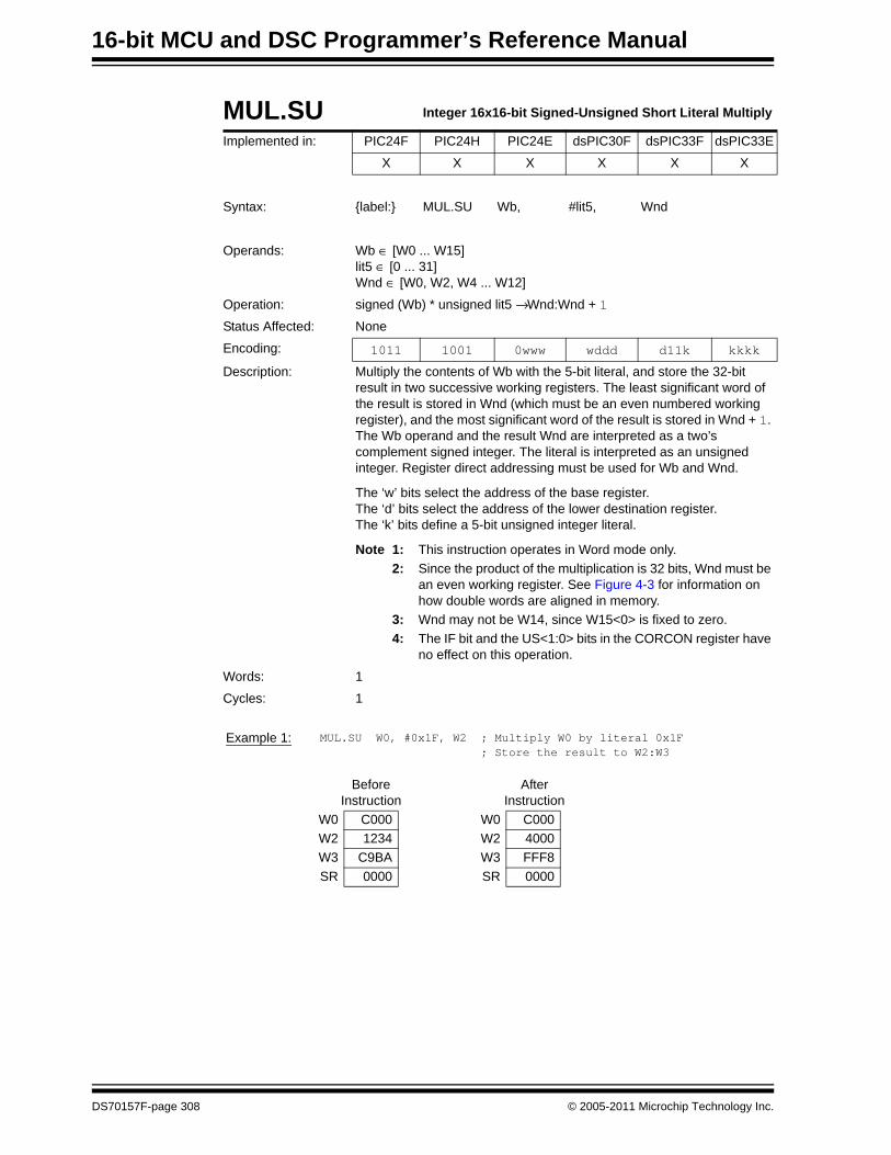
16-bit MCU and DSC Programmer’s Reference Manual
MUL.SU Integer 16x16-bit Signed-Unsigned Short Literal Multiply
Implemented in: PIC24F PIC24H PIC24E dsPIC30F dsPIC33F dsPIC33E
X X X X X X
Syntax: {label:} MUL.SU Wb, #lit5, Wnd
Operands: Wb ∈ [W0 ... W15]lit5 ∈ [0 ... 31]Wnd ∈ [W0, W2, W4 ... W12]
Operation: signed (Wb) * unsigned lit5 → Wnd:Wnd + 1
Status Affected: None
Encoding: 1011 1001 0www wddd d11k kkkk
Description: Multiply the contents of Wb with the 5-bit literal, and store the 32-bit result in two successive working registers. The least significant word of the result is stored in Wnd (which must be an even numbered working register), and the most significant word of the result is stored in Wnd + 1. The Wb operand and the result Wnd are interpreted as a two’s complement signed integer. The literal is interpreted as an unsigned integer. Register direct addressing must be used for Wb and Wnd.
The ‘w’ bits select the address of the base register.The ‘d’ bits select the address of the lower destination register.The ‘k’ bits define a 5-bit unsigned integer literal.
Note 1: This instruction operates in Word mode only.2: Since the product of the multiplication is 32 bits, Wnd must be
an even working register. See Figure 4-3 for information on how double words are aligned in memory.
3: Wnd may not be W14, since W15<0> is fixed to zero. 4: The IF bit and the US<1:0> bits in the CORCON register have
no effect on this operation.
Words: 1
Cycles: 1
Example 1: MUL.SU W0, #0x1F, W2 ; Multiply W0 by literal 0x1F ; Store the result to W2:W3
Before Instruction
After Instruction
W0 C000 W0 C000W2 1234 W2 4000W3 C9BA W3 FFF8SR 0000 SR 0000
DS70157F-page 308 © 2005-2011 Microchip Technology Inc.

Section 5. Instruction DescriptionsInstruction
Descriptions
5
Example 2: MUL.SU W2, #0x10, W0 ; Multiply W2 by literal 0x10 ; Store the result to W0:W1
Before Instruction
After Instruction
W0 ABCD W0 2400W1 89B3 W1 000FW2 F240 W2 F240SR 0000 SR 0000
© 2005-2011 Microchip Technology Inc. DS70157F-page 309

16-bit MCU and DSC Programmer’s Reference Manual
MUL.SU Integer 16x16-bit Signed-Unsigned Multiply
Implemented in: PIC24F PIC24H PIC24E dsPIC30F dsPIC33F dsPIC33E
X X X X X X
Syntax: {label:} MUL.SU Wb, Ws, Wnd
[Ws],
[Ws++],
[Ws--],
[++Ws],
[--Ws],
Operands: Wb ∈ [W0 ... W15]Ws ∈ [W0 ... W15] Wnd ∈ [W0, W2, W4 ... W12]
Operation: signed (Wb) * unsigned (Ws) → Wnd:Wnd + 1
Status Affected: None
Encoding: 1011 1001 0www wddd dppp ssss
Description: Multiply the contents of Wb with the contents of Ws, and store the 32-bit result in two successive working registers. The least significant word of the result is stored in Wnd (which must be an even numbered working register), and the most significant word of the result is stored in Wnd + 1. The Wb operand and the result Wnd are interpreted as a two’s complement signed integer. The Ws operand is interpreted as an unsigned integer. Register direct addressing must be used for Wb and Wnd. Register direct or register indirect addressing may be used for Ws.
The ‘w’ bits select the address of the base register.The ‘d’ bits select the address of the lower destination register.The ‘p’ bits select the source Address mode.The ‘s’ bits select the source register.
Note 1: This instruction operates in Word mode only.2: Since the product of the multiplication is 32 bits, Wnd must be
an even working register. See Figure 4-3 for information on how double words are aligned in memory.
3: Wnd may not be W14, since W15<0> is fixed to zero. 4: The IF bit and the US<1:0> bits in the CORCON register have
no effect on this operation.
Words: 1
Cycles: 1(1)
Note 1: In dsPIC33E and PIC24E devices, the listed cycle count does not apply to read and read-modify-write operations on non-CPU Special Function Registers. For more details, see Note 3 in Section 3.2.1 “Multi-Cycle Instructions”.
DS70157F-page 310 © 2005-2011 Microchip Technology Inc.

Section 5. Instruction DescriptionsInstruction
Descriptions
5
Example 1: MUL.SU W8, [W9], W0 ; Multiply W8*[W9] ; Store the result to W0:W1
Before Instruction
After Instruction
W0 68DC W0 0000W1 AA40 W1 F100W8 F000 W8 F000W9 178C W9 178C
Data 178C F000 Data 178C F000SR 0000 SR 0000
Example 2: MUL.SU W2, [++W3], W4 ; Pre-Increment W3 ; Multiply W2*[W3] ; Store the result to W4:W5
Before Instruction
After Instruction
W2 0040 W2 0040W3 0280 W3 0282W4 1819 W4 1A00W5 2021 W5 0000
Data 0282 0068 Data 0282 0068SR 0000 SR 0000
© 2005-2011 Microchip Technology Inc. DS70157F-page 311

16-bit MCU and DSC Programmer’s Reference Manual
MUL.SU Integer 16x16-bit Signed-Unsigned Multiply with Accumulator Destination
Implemented in: PIC24F PIC24H PIC24E dsPIC30F dsPIC33F dsPIC33E
X
Syntax: {label:} MUL.SU Wb, Ws,
[Ws], A
[Ws++], B
[Ws--],
[++Ws],
[--Ws],
Operands: Wb ∈ [W0 ... W15]Ws ∈ [W0 ... W15] ACC ∈ [A, B]
Operation: signed (Wb) * unsigned (Ws) → ACC(A or B)
Status Affected: None
Encoding: 1011 1001 0www w111 Appp ssss
Description: Performs a 16-bit x 16-bit signed multiply with a 32-bit result, which is stored in one of the DSP engine accumulators, ACCA or ACCB. The 32-bit result is sign extended to bit 39 prior to being loaded into the target accumulator.
The source operands are treated as integer or fractional values depending upon the operating mode of the DSP engine (as defined by the IF bit in CORCON<0>). The first source operand is interpreted as a two’s complement signed value and the second source operand is interpreted as an unsigned value.
The ‘w’ bits select the address of the base register.The ‘d’ bits select the address of the source register.The ‘p’ bits select source Address mode 2.The ‘A’ bit selects the destination accumulator for the product.
Note 1: This instruction operates in Word mode only.2: The state of the multiplier mode bits (US<1:0> in CORCON)
have no effect upon the operation of this instruction.
Words: 1
Cycles: 1(1)
Note 1: In dsPIC33E and PIC24E devices, the listed cycle count does not apply to read and read-modify-write operations on non-CPU Special Function Registers. For more details, see Note 3 in Section 3.2.1 “Multi-Cycle Instructions”.
DS70157F-page 312 © 2005-2011 Microchip Technology Inc.

Section 5. Instruction DescriptionsInstruction
Descriptions
5
Example 1: MUL.SU W8, W9, A
Before Instruction
After Instruction
W8 F000 W8 F000W9 F000 W9 F000
Acc A 00 0000 0000 Acc A FF F100 0000SR 0000 SR 0000
© 2005-2011 Microchip Technology Inc. DS70157F-page 313

16-bit MCU and DSC Programmer’s Reference Manual
MUL.SU Integer 16x16-bit Signed-Unsigned Short Literal Multiply with Accumulator Destination
Implemented in: PIC24F PIC24H PIC24E dsPIC30F dsPIC33F dsPIC33E
X
Syntax: {label:} MUL.SU Wb, #lit5, A
B
Operands: Wb ∈ [W0 ... W15]lit5 ∈ [0 ... 31] ACC ∈ [A, B]
Operation: signed (Wb) * unsigned (lit5) → ACC(A or B)
Status Affected: None
Encoding: 1011 1001 0www w111 A11k kkkk
Description: Performs a 16-bit x 16-bit signed multiply with a 32-bit result, which is stored in one of the DSP engine accumulators, ACCA or ACCB. The 32-bit result is sign extended to bit 39 prior to being loaded into the target accumulator.
The source operands are treated as integer or fractional values depending upon the operating mode of the DSP engine (as defined by the IF bit in CORCON<0>). The first source operand is interpreted as a two’s complement signed value and the second source operand is interpreted as an unsigned value.
The ‘w’ bits select the address of the base register.The ‘k’ bits select the 5-bit literal value.The ‘A’ bit selects the destination accumulator for the product.
Note 1: This instruction operates in Word mode only.2: The state of the multiplier mode bits (US<1:0> in CORCON)
have no effect upon the operation of this instruction.
Words: 1
Cycles: 1
Example 1: MUL.SU W8, #0x02, A
Before Instruction
After Instruction
W8 0042 W8 0042Acc A 00 0000 0000 Acc A 00 0000 0084
SR 0000 SR 0000
DS70157F-page 314 © 2005-2011 Microchip Technology Inc.

Section 5. Instruction DescriptionsInstruction
Descriptions
5
MUL.US Integer 16x16-bit Unsigned-Signed Multiply
Implemented in: PIC24F PIC24H PIC24E dsPIC30F dsPIC33F dsPIC33E
X X X X X X
Syntax: {label:} MUL.US Wb, Ws, Wnd
[Ws],
[Ws++],
[Ws--],
[++Ws],
[--Ws],
Operands: Wb ∈ [W0 ... W15]Ws ∈ [W0 ... W15] Wnd ∈ [W0, W2, W4 ... W12]
Operation: unsigned (Wb) * signed (Ws) → Wnd:Wnd + 1
Status Affected: None
Encoding: 1011 1000 1www wddd dppp ssss
Description: Multiply the contents of Wb with the contents of Ws, and store the 32-bit result in two successive working registers. The least significant word of the result is stored in Wnd (which must be an even numbered working register), and the most significant word of the result is stored in Wnd + 1. The Wb operand is interpreted as an unsigned integer. The Ws operand and the result Wnd are interpreted as a two’s complement signed integer. Register direct addressing must be used for Wb and Wnd. Register direct or register indirect addressing may be used for Ws.
The ‘w’ bits select the address of the base register.The ‘d’ bits select the address of the lower destination register.The ‘p’ bits select the source Address mode.The ‘s’ bits select the source register.
Note 1: This instruction operates in Word mode only.2: Since the product of the multiplication is 32 bits, Wnd must be
an even working register. See Figure 4-3 for information on how double words are aligned in memory.
3: Wnd may not be W14, since W15<0> is fixed to zero. 4: The IF bit and the US<1:0> bits in the CORCON register have
no effect on this operation.
Words: 1
Cycles: 1(1)
Note 1: In dsPIC33E and PIC24E devices, the listed cycle count does not apply to read and read-modify-write operations on non-CPU Special Function Registers. For more details, see Note 3 in Section 3.2.1 “Multi-Cycle Instructions”.
© 2005-2011 Microchip Technology Inc. DS70157F-page 315
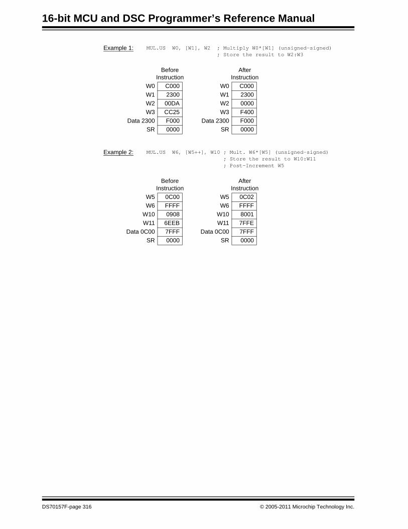
16-bit MCU and DSC Programmer’s Reference Manual
Example 1: MUL.US W0, [W1], W2 ; Multiply W0*[W1] (unsigned-signed) ; Store the result to W2:W3
Before Instruction
After Instruction
W0 C000 W0 C000W1 2300 W1 2300W2 00DA W2 0000W3 CC25 W3 F400
Data 2300 F000 Data 2300 F000SR 0000 SR 0000
Example 2: MUL.US W6, [W5++], W10 ; Mult. W6*[W5] (unsigned-signed) ; Store the result to W10:W11 ; Post-Increment W5
Before Instruction
After Instruction
W5 0C00 W5 0C02W6 FFFF W6 FFFF
W10 0908 W10 8001W11 6EEB W11 7FFE
Data 0C00 7FFF Data 0C00 7FFFSR 0000 SR 0000
DS70157F-page 316 © 2005-2011 Microchip Technology Inc.

Section 5. Instruction DescriptionsInstruction
Descriptions
5
MUL.US Integer 16x16-bit Unsigned-Signed Multiply with Accumulator Destination
Implemented in: PIC24F PIC24H PIC24E dsPIC30F dsPIC33F dsPIC33E
X
Syntax: {label:} MUL.US Wb, Ws, A
[Ws], B
[Ws++],
[Ws--],
[++Ws],
[--Ws],
Operands: Wb ∈ [W0 ... W15]Ws ∈ [W0 ... W15] ACC ∈ [A, B]
Operation: unsigned (Wb) * signed (Ws) → ACC(A or B)
Status Affected: None
Encoding: 1011 1000 0www w111 Appp ssss
Description: Performs a 16-bit x 16-bit signed multiply with a 32-bit result, which is stored in one of the DSP engine accumulators, ACCA or ACCB. The 32-bit result is sign extended to bit 39 prior to being loaded into the target accumulator.
The source operands are treated as integer or fractional values depending upon the operating mode of the DSP engine (as defined by the IF bit in CORCON<0>). The first source operand is interpreted as a unsigned value and the second source operand is interpreted as a two’s complement signed value.
The ‘w’ bits select the address of the base register.The ‘d’ bits select the address of the source register.The ‘p’ bits select source Address mode 2.The ‘A’ bit selects the destination accumulator for the product.
Note 1: This instruction operates in Word mode only.2: The state of the multiplier mode bits (US<1:0> in CORCON)
have no effect upon the operation of this instruction.
Words: 1
Cycles: 1(1)
Note 1: In dsPIC33E and PIC24E devices, the listed cycle count does not apply to read and read-modify-write operations on non-CPU Special Function Registers. For more details, see Note 3 in Section 3.2.1 “Multi-Cycle Instructions”.
© 2005-2011 Microchip Technology Inc. DS70157F-page 317

16-bit MCU and DSC Programmer’s Reference Manual
Example 1: MUL.US W0, W1, B
Before Instruction
After Instruction
W0 C000 W0 0000W1 F000 W1 F000
Acc B 00 0000 0000 Acc B FF F400 0000SR 0000 SR 0000
DS70157F-page 318 © 2005-2011 Microchip Technology Inc.

Section 5. Instruction DescriptionsInstruction
Descriptions
5
MUL.UU Integer 16x16-bit Unsigned Short Literal Multiply
Implemented in: PIC24F PIC24H PIC24E dsPIC30F dsPIC33F dsPIC33E
X X X X X X
Syntax: {label:} MUL.UU Wb, #lit5, Wnd
Operands: Wb ∈ [W0 ... W15]lit5 ∈ [0 ... 31]Wnd ∈ [W0, W2, W4 ... W12]
Operation: unsigned (Wb) * unsigned lit5 → Wnd:Wnd + 1
Status Affected: None
Encoding: 1011 1000 0www wddd d11k kkkk
Description: Multiply the contents of Wb with the 5-bit literal, and store the 32-bit result in two successive working registers. The least significant word of the result is stored in Wnd (which must be an even numbered working register), and the most significant word of the result is stored in Wnd + 1. Both operands and the result are interpreted as unsigned integers. Register direct addressing must be used for Wb and Wnd.
The ‘w’ bits select the address of the base register.The ‘d’ bits select the address of the lower destination register.The ‘k’ bits define a 5-bit unsigned integer literal.
Note 1: This instruction operates in Word mode only.2: Since the product of the multiplication is 32 bits, Wnd must be
an even working register. See Figure 4-3 for information on how double words are aligned in memory.
3: Wnd may not be W14, since W15<0> is fixed to zero. 4: The IF bit and the US<1:0> bits in the CORCON register have
no effect on this operation.
Words: 1
Cycles: 1
Example 1: MUL.UU W0, #0xF, W12 ; Multiply W0 by literal 0xF ; Store the result to W12:W13
Before Instruction
After Instruction
W0 2323 W0 2323W12 4512 W12 0F0DW13 7821 W13 0002
SR 0000 SR 0000
Example 2: MUL.UU W7, #0x1F, W0 ; Multiply W7 by literal 0x1F ; Store the result to W0:W1
Before Instruction
After Instruction
W0 780B W0 55C0W1 3805 W1 001DW7 F240 W7 F240SR 0000 SR 0000
© 2005-2011 Microchip Technology Inc. DS70157F-page 319

16-bit MCU and DSC Programmer’s Reference Manual
MUL.UU Integer 16x16-bit Unsigned Multiply
Implemented in: PIC24F PIC24H PIC24E dsPIC30F dsPIC33F dsPIC33E
X X X X X X
Syntax: {label:} MUL.UU Wb, Ws, Wnd
[Ws],
[Ws++],
[Ws--],
[++Ws],
[--Ws],
Operands: Wb ∈ [W0 ... W15]Ws ∈ [W0 ... W15] Wnd ∈ [W0, W2, W4 ... W12]
Operation: unsigned (Wb) * unsigned (Ws) → Wnd:Wnd + 1
Status Affected: None
Encoding: 1011 1000 0www wddd dppp ssss
Description: Multiply the contents of Wb with the contents of Ws, and store the 32-bit result in two successive working registers. The least significant word of the result is stored in Wnd (which must be an even numbered working register), and the most significant word of the result is stored in Wnd + 1. Both source operands and the result are interpreted as unsigned integers. Register direct addressing must be used for Wb and Wnd. Register direct or indirect addressing may be used for Ws.
The ‘w’ bits select the address of the base register.The ‘d’ bits select the address of the lower destination register.The ‘p’ bits select the source Address mode.The ‘s’ bits select the source register.
Note 1: This instruction operates in Word mode only.2: Since the product of the multiplication is 32 bits, Wnd must be
an even working register. See Figure 4-3 for information on how double words are aligned in memory.
3: Wnd may not be W14, since W15<0> is fixed to zero. 4: The IF bit and the US<1:0> bits in the CORCON register have
no effect on this operation.
Words: 1
Cycles: 1(1)
Note 1: In dsPIC33E and PIC24E devices, the listed cycle count does not apply to read and read-modify-write operations on non-CPU Special Function Registers. For more details, see Note 3 in Section 3.2.1 “Multi-Cycle Instructions”.
DS70157F-page 320 © 2005-2011 Microchip Technology Inc.

Section 5. Instruction DescriptionsInstruction
Descriptions
5
Example 1: MUL.UU W4, W0, W2 ; Multiply W4*W0 (unsigned-unsigned) ; Store the result to W2:W3
Before Instruction
After Instruction
W0 FFFF W0 FFFFW2 2300 W2 0001W3 00DA W3 FFFEW4 FFFF W4 FFFFSR 0000 SR 0000
Example 2: MUL.UU W0, [W1++], W4 ; Mult. W0*[W1] (unsigned-unsigned) ; Store the result to W4:W5 ; Post-Increment W1
Before Instruction
After Instruction
W0 1024 W0 1024W1 2300 W1 2302W4 9654 W4 6D34W5 BDBC W5 0D80
Data 2300 D625 Data 2300 D625SR 0000 SR 0000
© 2005-2011 Microchip Technology Inc. DS70157F-page 321
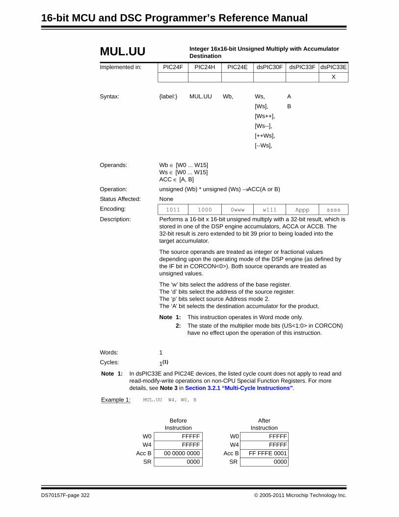
16-bit MCU and DSC Programmer’s Reference Manual
MUL.UU Integer 16x16-bit Unsigned Multiply with Accumulator Destination
Implemented in: PIC24F PIC24H PIC24E dsPIC30F dsPIC33F dsPIC33E
X
Syntax: {label:} MUL.UU Wb, Ws, A
[Ws], B
[Ws++],
[Ws--],
[++Ws],
[--Ws],
Operands: Wb ∈ [W0 ... W15]Ws ∈ [W0 ... W15] ACC ∈ [A, B]
Operation: unsigned (Wb) * unsigned (Ws) → ACC(A or B)
Status Affected: None
Encoding: 1011 1000 0www w111 Appp ssss
Description: Performs a 16-bit x 16-bit unsigned multiply with a 32-bit result, which is stored in one of the DSP engine accumulators, ACCA or ACCB. The 32-bit result is zero extended to bit 39 prior to being loaded into the target accumulator.
The source operands are treated as integer or fractional values depending upon the operating mode of the DSP engine (as defined by the IF bit in CORCON<0>). Both source operands are treated as unsigned values.
The ‘w’ bits select the address of the base register.The ‘d’ bits select the address of the source register.The ‘p’ bits select source Address mode 2.The ‘A’ bit selects the destination accumulator for the product.
Note 1: This instruction operates in Word mode only.2: The state of the multiplier mode bits (US<1:0> in CORCON)
have no effect upon the operation of this instruction.
Words: 1
Cycles: 1(1)
Note 1: In dsPIC33E and PIC24E devices, the listed cycle count does not apply to read and read-modify-write operations on non-CPU Special Function Registers. For more details, see Note 3 in Section 3.2.1 “Multi-Cycle Instructions”.
Example 1: MUL.UU W4, W0, B
Before Instruction
After Instruction
W0 FFFFF W0 FFFFFW4 FFFFF W4 FFFFF
Acc B 00 0000 0000 Acc B FF FFFE 0001SR 0000 SR 0000
DS70157F-page 322 © 2005-2011 Microchip Technology Inc.

Section 5. Instruction DescriptionsInstruction
Descriptions
5
MUL.UU Integer 16x16-bit Unsigned Short Literal Multiply with Accumulator Destination
Implemented in: PIC24F PIC24H PIC24E dsPIC30F dsPIC33F dsPIC33E
X
Syntax: {label:} MUL.UU Wb, #lit5, A
B
Operands: Wb ∈ [W0 ... W15]lit5 ∈ [0 ... 31] ACC ∈ [A, B]
Operation: unsigned (Wb) * unsigned (lit5) → ACC(A or B)
Status Affected: None
Encoding: 1011 1000 0www w111 A11k kkkk
Description: Performs a 16-bit x 16-bit signed multiply with a 32-bit result, which is stored in one of the DSP engine accumulators, ACCA or ACCB. The 32-bit result is zero extended to bit 39 prior to being loaded into the target accumulator.
The source operands are treated as integer or fractional values depending upon the operating mode of the DSP engine (as defined by the IF bit in CORCON<0>). Both source operands are treated as unsigned values.
The ‘w’ bits select the address of the base register.The ‘k’ bits select the 5-bit literal.The ‘A’ bit selects the destination accumulator for the product.
Note 1: This instruction operates in Word mode only.2: The state of the multiplier mode bits (US<1:0> in CORCON)
have no effect upon the operation of this instruction.
Words: 1
Cycles: 1
Example 1: MUL.UU W8, #0x02, A
Before Instruction
After Instruction
W8 0042 W8 0042Acc A 00 0000 0000 Acc A 00 0000 0084
SR 0000 SR 0000
© 2005-2011 Microchip Technology Inc. DS70157F-page 323

16-bit MCU and DSC Programmer’s Reference Manual
MULW.SS Integer 16x16-bit Signed Multiply with 16-bit Result
Implemented in: PIC24F PIC24H PIC24E dsPIC30F dsPIC33F dsPIC33E
X X
Syntax: {label:} MULW.SS Wb, Ws, Wnd
[Ws],
[Ws++],
[Ws--],
[++Ws],
[--Ws],
Operands: Wb ∈ [W0 ... W15]Ws ∈ [W0 ... W15] Wnd ∈ [W0, W2, W4 ... W12]
Operation: signed (Wb) * signed (Ws) → Wnd
Status Affected: None
Encoding: 1011 1001 1www wddd dppp ssss
Description: Multiply the contents of Wb with the contents of Ws, and store the result in a working register, which must be an even numbered working register. Both source operands and the result Wnd are interpreted as two’s complement signed integers. Register direct addressing must be used for Wb and Wnd. Register direct or register indirect addressing may be used for Ws.
The ‘w’ bits select the address of the base register.The ‘d’ bits select the address of the lower destination register.The ‘p’ bits select the source Address mode.The ‘s’ bits select the source register.
Note 1: This instruction operates in Word mode only.2: Wnd must be an even working register.3: Wnd may not be W14, since W15<0> is fixed to zero. 4: The IF bit and the US<1:0> bits in the CORCON register have
no effect on this operation.
Words: 1
Cycles: 1(1)
Note 1: In dsPIC33E and PIC24E devices, the listed cycle count does not apply to read and read-modify-write operations on non-CPU Special Function Registers. For more details, see Note 3 in Section 3.2.1 “Multi-Cycle Instructions”.
Example 1: MULW.SS W0, W1, W12 ; Multiply W0*W1; Store the result to W12
Before Instruction
After Instruction
W0 9823 W0 9823W1 67DC W1 67DC
W12 FFFF W12 D314SR 0000 SR 0000
DS70157F-page 324 © 2005-2011 Microchip Technology Inc.

Section 5. Instruction DescriptionsInstruction
Descriptions
5
Example 2: MULW.SS W2, [--W4], W0 ; Pre-decrement W4 ; Multiply W2*[W4] ; Store the result to W0
Before Instruction
After Instruction
W0 FFFF W0 28F8W2 0045 W2 0045W4 27FE W4 27FC
Data 27FC 0098 Data 27FC 0098SR 0000 SR 0000
© 2005-2011 Microchip Technology Inc. DS70157F-page 325
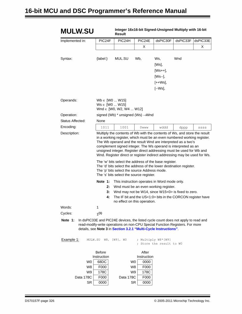
16-bit MCU and DSC Programmer’s Reference Manual
MULW.SU Integer 16x16-bit Signed-Unsigned Multiply with 16-bit Result
Implemented in: PIC24F PIC24H PIC24E dsPIC30F dsPIC33F dsPIC33E
X X
Syntax: {label:} MUL.SU Wb, Ws, Wnd
[Ws],
[Ws++],
[Ws--],
[++Ws],
[--Ws],
Operands: Wb ∈ [W0 ... W15]Ws ∈ [W0 ... W15] Wnd ∈ [W0, W2, W4 ... W12]
Operation: signed (Wb) * unsigned (Ws) → Wnd
Status Affected: None
Encoding: 1011 1001 0www wddd dppp ssss
Description: Multiply the contents of Wb with the contents of Ws, and store the result in a working register, which must be an even numbered working register. The Wb operand and the result Wnd are interpreted as a two’s complement signed integer. The Ws operand is interpreted as an unsigned integer. Register direct addressing must be used for Wb and Wnd. Register direct or register indirect addressing may be used for Ws.
The ‘w’ bits select the address of the base register.The ‘d’ bits select the address of the lower destination register.The ‘p’ bits select the source Address mode.The ‘s’ bits select the source register.
Note 1: This instruction operates in Word mode only.2: Wnd must be an even working register.3: Wnd may not be W14, since W15<0> is fixed to zero. 4: The IF bit and the US<1:0> bits in the CORCON register have
no effect on this operation.
Words: 1
Cycles: 1(1)
Note 1: In dsPIC33E and PIC24E devices, the listed cycle count does not apply to read and read-modify-write operations on non-CPU Special Function Registers. For more details, see Note 3 in Section 3.2.1 “Multi-Cycle Instructions”.
Example 1: MULW.SU W8, [W9], W0 ; Multiply W8*[W9]; Store the result to W0
Before Instruction
After Instruction
W0 68DC W0 0000W8 F000 W8 F000W9 178C W9 178C
Data 178C F000 Data 178C F000SR 0000 SR 0000
DS70157F-page 326 © 2005-2011 Microchip Technology Inc.

Section 5. Instruction DescriptionsInstruction
Descriptions
5
Example 2: MULW.SU W2, [++W3], W4 ; Pre-Increment W3 ; Multiply W2*[W3] ; Store the result to W4
Before Instruction
After Instruction
W2 0040 W2 0040W3 0280 W3 0282W4 1819 W4 1A00
Data 0282 0068 Data 0282 0068SR 0000 SR 0000
© 2005-2011 Microchip Technology Inc. DS70157F-page 327
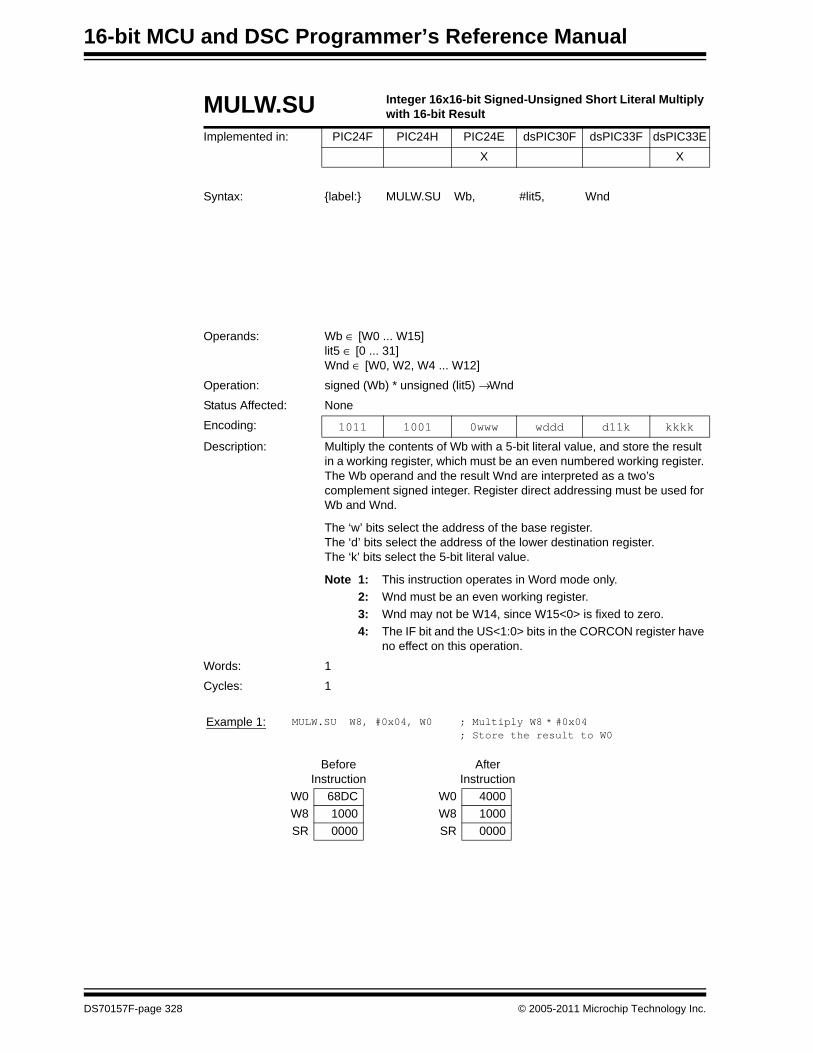
16-bit MCU and DSC Programmer’s Reference Manual
MULW.SU Integer 16x16-bit Signed-Unsigned Short Literal Multiply with 16-bit Result
Implemented in: PIC24F PIC24H PIC24E dsPIC30F dsPIC33F dsPIC33E
X X
Syntax: {label:} MULW.SU Wb, #lit5, Wnd
Operands: Wb ∈ [W0 ... W15]lit5 ∈ [0 ... 31] Wnd ∈ [W0, W2, W4 ... W12]
Operation: signed (Wb) * unsigned (lit5) → Wnd
Status Affected: None
Encoding: 1011 1001 0www wddd d11k kkkk
Description: Multiply the contents of Wb with a 5-bit literal value, and store the result in a working register, which must be an even numbered working register. The Wb operand and the result Wnd are interpreted as a two’s complement signed integer. Register direct addressing must be used for Wb and Wnd.
The ‘w’ bits select the address of the base register.The ‘d’ bits select the address of the lower destination register.The ‘k’ bits select the 5-bit literal value.
Note 1: This instruction operates in Word mode only.2: Wnd must be an even working register.3: Wnd may not be W14, since W15<0> is fixed to zero. 4: The IF bit and the US<1:0> bits in the CORCON register have
no effect on this operation.
Words: 1
Cycles: 1
Example 1: MULW.SU W8, #0x04, W0 ; Multiply W8 * #0x04; Store the result to W0
Before Instruction
After Instruction
W0 68DC W0 4000W8 1000 W8 1000SR 0000 SR 0000
DS70157F-page 328 © 2005-2011 Microchip Technology Inc.

Section 5. Instruction DescriptionsInstruction
Descriptions
5
MULW.US Integer 16x16-bit Unsigned-Signed Multiply with 16-bit Result
Implemented in: PIC24F PIC24H PIC24E dsPIC30F dsPIC33F dsPIC33E
X X
Syntax: {label:} MULW.US Wb, Ws, Wnd
[Ws],
[Ws++],
[Ws--],
[++Ws],
[--Ws],
Operands: Wb ∈ [W0 ... W15]Ws ∈ [W0 ... W15] Wnd ∈ [W0, W2, W4 ... W12]
Operation: unsigned (Wb) * signed (Ws) → Wnd
Status Affected: None
Encoding: 1011 1000 1www wddd dppp ssss
Description: Multiply the contents of Wb with the contents of Ws, and store the result in a working register, which must be an even numbered working register. The Wb operand is interpreted as an unsigned integer. The Ws operand and the result Wnd are interpreted as a two’s complement signed integer. Register direct addressing must be used for Wb and Wnd. Register direct or register indirect addressing may be used for Ws.
The ‘w’ bits select the address of the base register.The ‘d’ bits select the address of the lower destination register.The ‘p’ bits select the source Address mode.The ‘s’ bits select the source register.
Note 1: This instruction operates in Word mode only.2: Wnd must be an even working register.3: Wnd may not be W14, since W15<0> is fixed to zero. 4: The IF bit and the US<1:0> bits in the CORCON register have
no effect on this operation.
Words: 1
Cycles: 1(1)
Note 1: In dsPIC33E and PIC24E devices, the listed cycle count does not apply to read and read-modify-write operations on non-CPU Special Function Registers. For more details, see Note 3 in Section 3.2.1 “Multi-Cycle Instructions”.
Example 1: MULW.US W0, [W1], W2 ; Multiply W0*[W1] (unsigned-signed) ; Store the result to W2
Before Instruction
After Instruction
W0 C000 W0 C000W1 2300 W1 2300W2 00DA W2 0000
Data 2300 F000 Data 2300 F000SR 0000 SR 0000
© 2005-2011 Microchip Technology Inc. DS70157F-page 329

16-bit MCU and DSC Programmer’s Reference Manual
Example 2: MULW.US W6, [W5++], W10 ; Mult. W6*[W5] (unsigned-signed); Store the result to W10; Post-Increment W5
Before Instruction
After Instruction
W5 0C00 W5 0C02W6 FFFF W6 FFFF
W10 0908 W10 8001Data 0C00 7FFF Data 0C00 7FFF
SR 0000 SR 0000
DS70157F-page 330 © 2005-2011 Microchip Technology Inc.

Section 5. Instruction DescriptionsInstruction
Descriptions
5
MULW.UU Integer 16x16-bit Unsigned Multiply with 16-bit Result
Implemented in: PIC24F PIC24H PIC24E dsPIC30F dsPIC33F dsPIC33EX X
Syntax: {label:} MULW.UU Wb, Ws, Wnd[Ws],[Ws++],[Ws--],[++Ws],[--Ws],
Operands: Wb ∈ [W0 ... W15]Ws ∈ [W0 ... W15] Wnd ∈ [W0, W2, W4 ... W12]
Operation: unsigned (Wb) * unsigned (Ws) → WndStatus Affected: NoneEncoding: 1011 1000 0www wddd dppp ssss
Description: Multiply the contents of Wb with the contents of Ws, and store the result in a working registers, which must be an even numbered working register). Both source operands and the result are interpreted as unsigned integers. Register direct addressing must be used for Wb and Wnd. Register direct or indirect addressing may be used for Ws.
The ‘w’ bits select the address of the base register.The ‘d’ bits select the address of the lower destination register.The ‘p’ bits select the source Address mode.The ‘s’ bits select the source register.
Note 1: This instruction operates in Word mode only.2: Wnd must be an even working register.3: Wnd may not be W14, since W15<0> is fixed to zero. 4: The IF bit and the US<1:0> bits in the CORCON register have
no effect on this operation.Words: 1Cycles: 1(1)
Note 1: In dsPIC33E and PIC24E devices, the listed cycle count does not apply to read and read-modify-write operations on non-CPU Special Function Registers. For more details, see Note 3 in Section 3.2.1 “Multi-Cycle Instructions”.
Example 1: MULW.UU W4, W0, W2 ; Multiply W4*W0 (unsigned-unsigned) ; Store the result to W2
Before Instruction
After Instruction
W0 FFFF W0 FFFFW2 2300 W2 0001W4 FFFF W4 FFFFSR 0000 SR 0000
© 2005-2011 Microchip Technology Inc. DS70157F-page 331

16-bit MCU and DSC Programmer’s Reference Manual
MULW.UU Integer 16x16-bit Unsigned Short Literal Multiply with 16-bit Result
Implemented in: PIC24F PIC24H PIC24E dsPIC30F dsPIC33F dsPIC33EX X
Syntax: {label:} MULW.UU Wb, #lit5, Wnd
Operands: Wb ∈ [W0 ... W15]lit5 ∈ [0 ... 31] Wnd ∈ [W0, W2, W4 ... W12]
Operation: unsigned (Wb) * unsigned → WndStatus Affected: NoneEncoding: 1011 1000 0www wddd d11k kkkk
Description: Multiply the contents of Wb with a 5-bit literal value, and store the result in a working registers, which must be an even numbered working register). Both source operands and the result are interpreted as unsigned integers. Register direct addressing must be used for Wb and Wnd.
The ‘w’ bits select the address of the base register.The ‘d’ bits select the address of the lower destination register.The ‘k’ bits select the 5-bit literal value.
Note 1: This instruction operates in Word mode only.2: Wnd must be an even working register.3: Wnd may not be W14, since W15<0> is fixed to zero. 4: The IF bit and the US<1:0> bits in the CORCON register have
no effect on this operation.Words: 1Cycles: 1
Example 1: MULW.UU W4, #0x04, W2 ; Multiply W4*W0 (unsigned-unsigned) ; Store the result to W2
Before Instruction
After Instruction
W2 2300 W2 4000W4 1000 W4 1000SR 0000 SR 0000
DS70157F-page 332 © 2005-2011 Microchip Technology Inc.

Section 5. Instruction DescriptionsInstruction
Descriptions
5
NEG Negate f
Implemented in: PIC24F PIC24H PIC24E dsPIC30F dsPIC33F dsPIC33E
X X X X X X
Syntax: {label:} NEG{.B} f {,WREG}
Operands: f ∈ [0 ... 8191]
Operation: (f) + 1 → destination designated by D
Status Affected: DC, N, OV, Z, C
Encoding: 1110 1110 0BDf ffff ffff ffff
Description: Compute the two’s complement of the contents of the file register and place the result in the destination register. The optional WREG operand determines the destination register. If WREG is specified, the result is stored in WREG. If WREG is not specified, the result is stored in the file register.
The ‘B’ bit selects byte or word operation (‘0’ for word, ‘1’ for byte).The ‘D’ bit selects the destination (‘0’ for WREG, ‘1’ for file register).The ‘f’ bits select the address of the file register.
Note 1: The extension .B in the instruction denotes a byte operation rather than a word operation. You may use a .W extension to denote a word operation, but it is not required.
2: The WREG is set to working register W0.
Words: 1
Cycles: 1(1)
Note 1: In dsPIC33E and PIC24E devices, the listed cycle count does not apply to read and read-modify-write operations on non-CPU Special Function Registers. For more details, see Note 3 in Section 3.2.1 “Multi-Cycle Instructions”.
Example 1: NEG.B 0x880, WREG ; Negate (0x880) (Byte mode) ; Store result to WREG
Before Instruction
After Instruction
WREG (W0) 9080 WREG (W0) 90ABData 0880 2355 Data 0880 2355
SR 0000 SR 0008 (N = 1)Example 2: NEG 0x1200 ; Negate (0x1200) (Word mode)
Before Instruction
After Instruction
Data 1200 8923 Data 1200 76DDSR 0000 SR 0000
NEG Negate Ws
Implemented in: PIC24F PIC24H PIC24E dsPIC30F dsPIC33F dsPIC33EX X X X X X
Syntax: {label:} NEG{.B} Ws, Wd[Ws], [Wd]
© 2005-2011 Microchip Technology Inc. DS70157F-page 333

16-bit MCU and DSC Programmer’s Reference Manual
[Ws++], [Wd++][Ws--], [Wd--][++Ws], [++Wd][--Ws], [--Wd]
Operands: Ws ∈ [W0 ... W15]Wd ∈ [W0 ... W15]
Operation: (Ws) + 1 → Wd Status Affected: DC, N, OV, Z, CEncoding: 1110 1010 0Bqq qddd dppp ssss
Description: Compute the two’s complement of the contents of the source register Ws and place the result in the destination register Wd. Either register direct or indirect addressing may be used for both Ws and Wd.
The ‘B’ bit selects byte or word operation (‘0’ for word, ‘1’ for byte).The ‘q’ bits select the destination Address mode.The ‘d’ bits select the destination register.The ‘p’ bits select the source Address mode.The ‘s’ bits select the source register.
Note: The extension .B in the instruction denotes a byte operation rather than a word operation. You may use a .W extension to denote a word operation, but it is not required.
Words: 1Cycles: 1(1)
Note 1: In dsPIC33E and PIC24E devices, the listed cycle count does not apply to read and read-modify-write operations on non-CPU Special Function Registers. For more details, see Note 3 in Section 3.2.1 “Multi-Cycle Instructions”.
Example 1: NEG.B W3, [W4++] ; Negate W3 and store to [W4] (Byte mode) ; Post-increment W4
Before Instruction
After Instruction
W3 7839 W3 7839W4 1005 W4 1006
Data 1004 2355 Data 1004 C755SR 0000 SR 0008 (N = 1)
NEG Negate Ws
Example 2: NEG [W2++], [--W4] ; Pre-decrement W4 (Word mode) ; Negate [W2] and store to [W4] ; Post-increment W2
Before Instruction
After Instruction
W2 0900 W2 0902W4 1002 W4 1000
Data 0900 870F Data 0900 870FData 1000 5105 Data 1000 78F1
SR 0000 SR 0000
DS70157F-page 334 © 2005-2011 Microchip Technology Inc.

Section 5. Instruction DescriptionsInstruction
Descriptions
5
NEG Negate Accumulator
Implemented in: PIC24F PIC24H PIC24E dsPIC30F dsPIC33F dsPIC33E
X X X
Syntax: {label:} NEG Acc
Operands: Acc ∈ [A,B]
Operation: If (Acc = A): -ACCA → ACCAElse: -ACCB → ACCB
Status Affected: OA, OB, OAB, SA, SB, SAB
Encoding: 1100 1011 A001 0000 0000 0000
Description: Compute the two’s complement of the contents of the specified accumulator. Regardless of the Saturation mode, this instruction operates on all 40 bits of the accumulator.
The ‘A’ bit specifies the selected accumulator.
Words: 1
Cycles: 1
Example 1: NEG A ; Negate ACCA ; Store result to ACCA ; CORCON = 0x0000 (no saturation)
Before Instruction
After Instruction
ACCA 00 3290 59C8 ACCA FF CD6F A638CORCON 0000 CORCON 0000
SR 0000 SR 0000
Example 2: NEG B ; Negate ACCB ; Store result to ACCB ; CORCON = 0x00C0 (normal saturation)
Before Instruction
After Instruction
ACCB FF F230 10DC ACCB 00 0DCF EF24CORCON 00C0 CORCON 00C0
SR 0000 SR 0000
© 2005-2011 Microchip Technology Inc. DS70157F-page 335

16-bit MCU and DSC Programmer’s Reference Manual
NOP No Operation
Implemented in: PIC24F PIC24H PIC24E dsPIC30F dsPIC33F dsPIC33E
X X X X X X
Syntax: {label:} NOP
Operands: None
Operation: No Operation
Status Affected: None
Encoding: 0000 0000 xxxx xxxx xxxx xxxx
Description: No Operation is performed.
The ‘x’ bits can take any value.
Words: 1
Cycles: 1
Example 1: NOP ; execute no operation
Before Instruction
After Instruction
PC 00 1092 PC 00 1094SR 0000 SR 0000
Example 2: NOP ; execute no operation
Before Instruction
After Instruction
PC 00 08AE PC 00 08B0SR 0000 SR 0000
NOPR No Operation
Implemented in: PIC24F PIC24H PIC24E dsPIC30F dsPIC33F dsPIC33E
X X X X X X
Syntax: {label:} NOPR
Operands: None
Operation: No Operation
Status Affected: None
Encoding: 1111 1111 xxxx xxxx xxxx xxxx
Description: No Operation is performed.
The ‘x’ bits can take any value.
Words: 1
Cycles: 1
DS70157F-page 336 © 2005-2011 Microchip Technology Inc.

Section 5. Instruction DescriptionsInstruction
Descriptions
5
Example 1: NOPR ; execute no operation
Before Instruction
After Instruction
PC 00 2430 PC 00 2432SR 0000 SR 0000
Example 2: NOPR ; execute no operation
Before Instruction
After Instruction
PC 00 1466 PC 00 1468SR 0000 SR 0000
POP Pop TOS to f
Implemented in: PIC24F PIC24H PIC24E dsPIC30F dsPIC33F dsPIC33E
X X X X X X
Syntax: {label:} POP f
Operands: f ∈ [0 ... 65534]
Operation: (W15) – 2 → W15(TOS) → f
Status Affected: None
Encoding: 1111 1001 ffff ffff ffff fff0
Description: The Stack Pointer (W15) is pre-decremented by 2 and the Top-of-Stack (TOS) word is written to the specified file register, which may reside anywhere in the lower 32K words of data memory.
The ‘f’ bits select the address of the file register.
Note 1: This instruction operates in Word mode only.2: The file register address must be word-aligned.
Words: 1
Cycles: 1
Example 1: POP 0x1230 ; Pop TOS to 0x1230
Before Instruction
After Instruction
W15 1006 W15 1004Data 1004 A401 Data 1004 A401Data 1230 2355 Data 1230 A401
SR 0000 SR 0000
© 2005-2011 Microchip Technology Inc. DS70157F-page 337

16-bit MCU and DSC Programmer’s Reference Manual
Example 2: POP 0x880 ; Pop TOS to 0x880
Before Instruction
After Instruction
W15 2000 W15 1FFEData 0880 E3E1 Data 0880 A090Data 1FFE A090 Data 1FFE A090
SR 0000 SR 0000
POP Pop TOS to Wd
Implemented in: PIC24F PIC24H PIC24E dsPIC30F dsPIC33F dsPIC33EX X X X X X
Syntax: {label:} POP Wd[Wd][Wd++][Wd--][--Wd][++Wd][Wd+Wb]
Operands: Wd ∈ [W0 ... W15]Wb ∈ [W0 ... W15]
Operation: (W15) – 2 → W15(TOS) → Wd
Status Affected: NoneEncoding: 0111 1www w0hh hddd d100 1111
Description: The Stack Pointer (W15) is pre-decremented by 2 and the Top-of-Stack (TOS) word is written to Wd. Either register direct or indirect addressing may be used for Wd.
The ‘w’ bits define the offset register Wb.The ‘h’ bits select the destination Address mode.The ‘d’ bits select the destination register.
Note 1: This instruction operates in Word mode only.2: This instruction is a specific version of the “MOV Ws, Wd”
instruction (MOV [--W15], Wd). It reverse assembles as MOV.
Words: 1Cycles: 1
Example 1: POP W4 ; Pop TOS to W4
Before Instruction
After Instruction
W4 EDA8 W4 C45AW15 1008 W15 1006
Data 1006 C45A Data 1006 C45ASR 0000 SR 0000
DS70157F-page 338 © 2005-2011 Microchip Technology Inc.

Section 5. Instruction DescriptionsInstruction
Descriptions
5
Example 2: POP [++W10] ; Pre-increment W10 ; Pop TOS to [W10]
Before Instruction
After Instruction
W10 0E02 W10 0E04W15 1766 W15 1764
Data 0E04 E3E1 Data 0E04 C7B5Data 1764 C7B5 Data 1764 C7B5
SR 0000 SR 0000
POP.D Double Pop TOS to Wnd:Wnd+1
Implemented in: PIC24F PIC24H PIC24E dsPIC30F dsPIC33F dsPIC33E
X X X X X X
Syntax: {label:} POP.D Wnd
Operands: Wnd ∈ [W0, W2, W4, ... W14]
Operation: (W15) – 2 → W15(TOS) → Wnd + 1(W15) – 2 → W15(TOS) → Wnd
Status Affected: None
Encoding: 1011 1110 0000 0ddd 0100 1111
Description: A double word is POPped from the Top-of-Stack (TOS) and stored to Wnd:Wnd + 1. The most significant word is stored to Wnd + 1, and the least significant word is stored to Wnd. Since a double word is POPped, the Stack Pointer (W15) gets decremented by 4.
The ‘d’ bits select the address of the destination register pair.
Note 1: This instruction operates on double words. See Figure 4-3 for information on how double words are aligned in memory.
2: Wnd must be an even working register.3: This instruction is a specific version of the “MOV.D Ws, Wnd”
instruction (MOV.D [--W15], Wnd). It reverse assembles as MOV.D.
Words: 1
Cycles: 2
Example 1: POP.D W6 ; Double pop TOS to W6
Before Instruction
After Instruction
W6 07BB W6 3210W7 89AE W7 7654
W15 0850 W15 084CData 084C 3210 Data 084C 3210Data 084E 7654 Data 084E 7654
SR 0000 SR 0000
© 2005-2011 Microchip Technology Inc. DS70157F-page 339
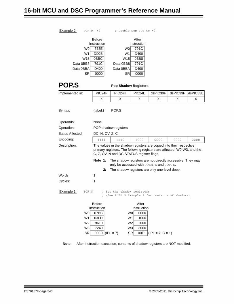
16-bit MCU and DSC Programmer’s Reference Manual
Example 2: POP.D W0 ; Double pop TOS to W0
Before Instruction
After Instruction
W0 673E W0 791CW1 DD23 W1 D400
W15 0BBC W15 0BB8Data 0BB8 791C Data 0BB8 791CData 0BBA D400 Data 0BBA D400
SR 0000 SR 0000
POP.S Pop Shadow Registers
Implemented in: PIC24F PIC24H PIC24E dsPIC30F dsPIC33F dsPIC33E
X X X X X X
Syntax: {label:} POP.S
Operands: None
Operation: POP shadow registers
Status Affected: DC, N, OV, Z, C
Encoding: 1111 1110 1000 0000 0000 0000
Description: The values in the shadow registers are copied into their respective primary registers. The following registers are affected: W0-W3, and the C, Z, OV, N and DC STATUS register flags.
Note 1: The shadow registers are not directly accessible. They may only be accessed with PUSH.S and POP.S.
2: The shadow registers are only one-level deep.
Words: 1
Cycles: 1
Example 1: POP.S ; Pop the shadow registers ; (See PUSH.S Example 1 for contents of shadows)
Before Instruction
After Instruction
W0 07BB W0 0000W1 03FD W1 1000W2 9610 W2 2000W3 7249 W3 3000SR 00E0 (IPL = 7) SR 00E1 (IPL = 7, C = 1)
Note: After instruction execution, contents of shadow registers are NOT modified.
DS70157F-page 340 © 2005-2011 Microchip Technology Inc.
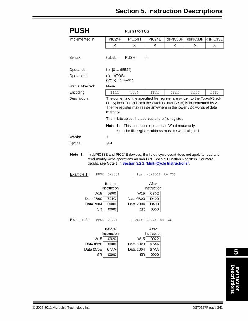
Section 5. Instruction DescriptionsInstruction
Descriptions
5
PUSH Push f to TOS
Implemented in: PIC24F PIC24H PIC24E dsPIC30F dsPIC33F dsPIC33E
X X X X X X
Syntax: {label:} PUSH f
Operands: f ∈ [0 ... 65534]
Operation: (f) → (TOS)(W15) + 2 → W15
Status Affected: None
Encoding: 1111 1000 ffff ffff ffff fff0
Description: The contents of the specified file register are written to the Top-of-Stack (TOS) location and then the Stack Pointer (W15) is incremented by 2.The file register may reside anywhere in the lower 32K words of data memory.
The ‘f’ bits select the address of the file register.
Note 1: This instruction operates in Word mode only.2: The file register address must be word-aligned.
Words: 1
Cycles: 1(1)
Note 1: In dsPIC33E and PIC24E devices, the listed cycle count does not apply to read and read-modify-write operations on non-CPU Special Function Registers. For more details, see Note 3 in Section 3.2.1 “Multi-Cycle Instructions”.
Example 1: PUSH 0x2004 ; Push (0x2004) to TOS
Before Instruction
After Instruction
W15 0B00 W15 0B02Data 0B00 791C Data 0B00 D400Data 2004 D400 Data 2004 D400
SR 0000 SR 0000
Example 2: PUSH 0xC0E ; Push (0xC0E) to TOS
Before Instruction
After Instruction
W15 0920 W15 0922Data 0920 0000 Data 0920 67AA
Data 0C0E 67AA Data 2004 67AASR 0000 SR 0000
© 2005-2011 Microchip Technology Inc. DS70157F-page 341

16-bit MCU and DSC Programmer’s Reference Manual
PUSH Push Ws to TOS
Implemented in: PIC24F PIC24H PIC24E dsPIC30F dsPIC33F dsPIC33E
X X X X X X
Syntax: {label:} PUSH Ws
[Ws]
[Ws++]
[Ws--]
[--Ws]
[++Ws]
[Ws+Wb]
Operands: Ws ∈ [W0 ... W15]Wb ∈ [W0 ... W15]
Operation: (Ws) → (TOS)(W15) + 2 → W15
Status Affected: None
Encoding: 0111 1www w001 1111 1ggg ssss
Description: The contents of Ws are written to the Top-of-Stack (TOS) location and then the Stack Pointer (W15) is incremented by 2.
The ‘w’ bits define the offset register Wb.The ‘g’ bits select the source Address mode.The ‘s’ bits select the source register.
Note 1: This instruction operates in Word mode only.2: This instruction is a specific version of the “MOV Ws, Wd”
instruction (MOV Ws, [W15++]). It reverse assembles as MOV.
Words: 1
Cycles: 1(1)
Note 1: In dsPIC33E and PIC24E devices, the listed cycle count does not apply to read and read-modify-write operations on non-CPU Special Function Registers. For more details, see Note 3 in Section 3.2.1 “Multi-Cycle Instructions”.
Example 1: PUSH W2 ; Push W2 to TOS
Before Instruction
After Instruction
W2 6889 W2 6889W15 1566 W15 1568
Data 1566 0000 Data 1566 6889SR 0000 SR 0000
DS70157F-page 342 © 2005-2011 Microchip Technology Inc.

Section 5. Instruction DescriptionsInstruction
Descriptions
5
Example 2: PUSH [W5+W10] ; Push [W5+W10] to TOS
Before Instruction
After Instruction
W5 1200 W5 1200W10 0044 W10 0044W15 0806 W15 0808
Data 0806 216F Data 0806 B20AData 1244 B20A Data 1244 B20A
SR 0000 SR 0000
PUSH.D Double Push Wns:Wns+1 to TOS
Implemented in: PIC24F PIC24H PIC24E dsPIC30F dsPIC33F dsPIC33E
X X X X X X
Syntax: {label:} PUSH.D Wns
Operands: Wns ∈ [W0, W2, W4 ... W14]
Operation: (Wns) → (TOS)(W15) + 2 → W15(Wns + 1) → (TOS)(W15) + 2 → W15
Status Affected: None
Encoding: 1011 1110 1001 1111 1000 sss0
Description: A double word (Wns:Wns + 1) is PUSHed to the Top-of-Stack (TOS). The least significant word (Wns) is PUSHed to the TOS first, and the most significant word (Wns + 1) is PUSHed to the TOS last. Since a double word is PUSHed, the Stack Pointer (W15) gets incremented by 4.
The ‘s’ bits select the address of the source register pair.
Note 1: This instruction operates on double words. See Figure 4-3 for information on how double words are aligned in memory.
2: Wns must be an even working register.3: This instruction is a specific version of the “MOV.D Wns, Wd”
instruction (MOV.D Wns, [W15++]). It reverse assembles as MOV.D.
Words: 1
Cycles: 2
Example 1: PUSH.D W6 ; Push W6:W7 to TOS
Before Instruction
After Instruction
W6 C451 W6 C451W7 3380 W7 3380
W15 1240 W15 1244Data 1240 B004 Data 1240 C451Data 1242 0891 Data 1242 3380
SR 0000 SR 0000
© 2005-2011 Microchip Technology Inc. DS70157F-page 343

16-bit MCU and DSC Programmer’s Reference Manual
Example 2: PUSH.D W10 ; Push W10:W11 to TOS
Before Instruction
After Instruction
W10 80D3 W10 80D3W11 4550 W11 4550W15 0C08 W15 0C0C
Data 0C08 79B5 Data 0C08 80D3Data 0C0A 008E Data 0C0A 4550
SR 0000 SR 0000
DS70157F-page 344 © 2005-2011 Microchip Technology Inc.

Section 5. Instruction DescriptionsInstruction
Descriptions
5
PUSH.S Push Shadow Registers
Implemented in: PIC24F PIC24H PIC24E dsPIC30F dsPIC33F dsPIC33E
X X X X X X
Syntax: {label:} PUSH.S
Operands: None
Operation: PUSH shadow registers
Status Affected: None
Encoding: 1111 1110 1010 0000 0000 0000
Description: The contents of the primary registers are copied into their respective shadow registers. The following registers are shadowed: W0-W3, and the C, Z, OV, N and DC STATUS register flags.
Note 1: The shadow registers are not directly accessible. They may only be accessed with PUSH.S and POP.S.
2: The shadow registers are only one-level deep.
Words: 1
Cycles: 1
Example 1: PUSH.S ; Push primary registers into shadow registers
Before Instruction
After Instruction
W0 0000 W0 0000W1 1000 W1 1000W2 2000 W2 2000W3 3000 W3 3000SR 0001 (C = 1) SR 0001 (C = 1)
Note: After an instruction execution, contents of the shadow registers are updated.
© 2005-2011 Microchip Technology Inc. DS70157F-page 345
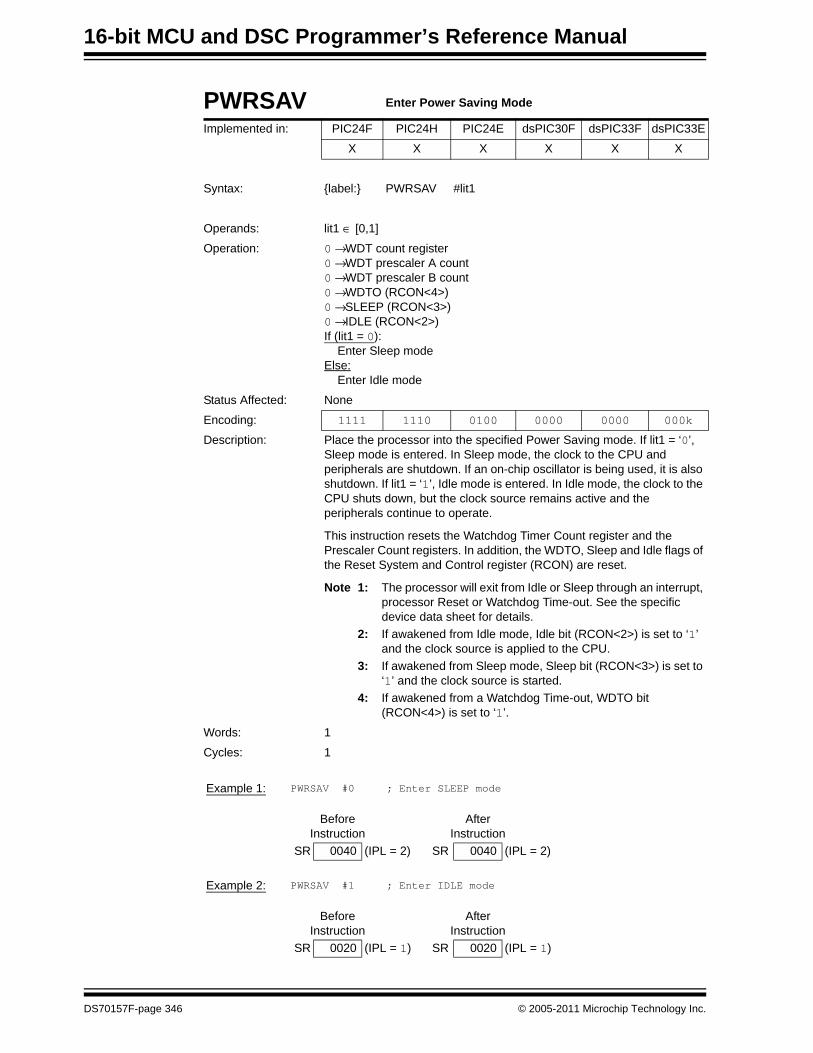
16-bit MCU and DSC Programmer’s Reference Manual
PWRSAV Enter Power Saving Mode
Implemented in: PIC24F PIC24H PIC24E dsPIC30F dsPIC33F dsPIC33E
X X X X X X
Syntax: {label:} PWRSAV #lit1
Operands: lit1 ∈ [0,1]
Operation: 0 → WDT count register0 → WDT prescaler A count0 → WDT prescaler B count0 → WDTO (RCON<4>)0 → SLEEP (RCON<3>)0 → IDLE (RCON<2>)If (lit1 = 0): Enter Sleep modeElse: Enter Idle mode
Status Affected: None
Encoding: 1111 1110 0100 0000 0000 000k
Description: Place the processor into the specified Power Saving mode. If lit1 = ‘0’, Sleep mode is entered. In Sleep mode, the clock to the CPU and peripherals are shutdown. If an on-chip oscillator is being used, it is also shutdown. If lit1 = ‘1’, Idle mode is entered. In Idle mode, the clock to the CPU shuts down, but the clock source remains active and the peripherals continue to operate.
This instruction resets the Watchdog Timer Count register and the Prescaler Count registers. In addition, the WDTO, Sleep and Idle flags of the Reset System and Control register (RCON) are reset.
Note 1: The processor will exit from Idle or Sleep through an interrupt, processor Reset or Watchdog Time-out. See the specific device data sheet for details.
2: If awakened from Idle mode, Idle bit (RCON<2>) is set to ‘1’ and the clock source is applied to the CPU.
3: If awakened from Sleep mode, Sleep bit (RCON<3>) is set to ‘1’ and the clock source is started.
4: If awakened from a Watchdog Time-out, WDTO bit (RCON<4>) is set to ‘1’.
Words: 1
Cycles: 1
Example 1: PWRSAV #0 ; Enter SLEEP mode
Before Instruction
After Instruction
SR 0040 (IPL = 2) SR 0040 (IPL = 2)
Example 2: PWRSAV #1 ; Enter IDLE mode
Before Instruction
After Instruction
SR 0020 (IPL = 1) SR 0020 (IPL = 1)
DS70157F-page 346 © 2005-2011 Microchip Technology Inc.

Section 5. Instruction DescriptionsInstruction
Descriptions
5
RCALL Relative Call
Implemented in: PIC24F PIC24H PIC24E dsPIC30F dsPIC33F dsPIC33E
X X X X
Syntax: {label:} RCALL Expr
Operands: Expr may be an absolute address, label or expression.Expr is resolved by the linker to a Slit16, where Slit16 ∈ [-32768 ... 32767].
Operation: (PC) + 2 → PC(PC<15:0>) → (TOS)(W15) + 2 → W15(PC<22:16>) → (TOS)(W15) + 2 → W15(PC) + (2 * Slit16) → PCNOP → Instruction Register
Status Affected: None
Encoding: 0000 0111 nnnn nnnn nnnn nnnn
Description: Relative subroutine call with a range of 32K program words forward or back from the current PC. Before the call is made, the return address (PC + 2) is PUSHed onto the stack. After the return address is stacked, the sign-extended 17-bit value (2 * Slit16) is added to the contents of the PC and the result is stored in the PC.
The ‘n’ bits are a signed literal that specifies the size of the relative call (in program words) from (PC + 2).
Note: When possible, this instruction should be used instead of CALL,since it only consumes one word of program memory.
Words: 1
Cycles: 2
Example 1: 012004 RCALL _Task1012006 ADD W0, W1, W2 . ... . ...012458 _Task1: SUB W0, W2, W301245A ...
; Call _Task1
; _Task1 subroutine
Before Instruction
After Instruction
PC 01 2004 PC 01 2458W15 0810 W15 0814
Data 0810 FFFF Data 0810 2006Data 0812 FFFF Data 0812 0001
SR 0000 SR 0000
© 2005-2011 Microchip Technology Inc. DS70157F-page 347

16-bit MCU and DSC Programmer’s Reference Manual
Example 2: 00620E RCALL _Init006210 MOV W0, [W4++] . ... . ...007000 _Init: CLR W2007002 ...
; Call _Init
; _Init subroutine
Before Instruction
After Instruction
PC 00 620E PC 00 7000W15 0C50 W15 0C54
Data 0C50 FFFF Data 0C50 6210Data 0C52 FFFF Data 0C52 0000
SR 0000 SR 0000
DS70157F-page 348 © 2005-2011 Microchip Technology Inc.

Section 5. Instruction DescriptionsInstruction
Descriptions
5
RCALL Relative Call
Implemented in: PIC24F PIC24H PIC24E dsPIC30F dsPIC33F dsPIC33E
X X
Syntax: {label:} RCALL Expr
Operands: Expr may be an absolute address, label or expression.Expr is resolved by the linker to a Slit16, where Slit16 ∈ [-32768 ... 32767].
Operation: (PC) + 2 → PC(PC<15:1>) → TOS<15:1>, SFA bit → TOS<0>(W15) + 2 → W15(PC<22:16>) → (TOS)(W15) + 2 → W150 → SFA bit(PC) + (2 * Slit16) → PCNOP → Instruction Register
Status Affected: SFA
Encoding: 0000 0111 nnnn nnnn nnnn nnnn
Description: Relative subroutine call with a range of 32K program words forward or back from the current PC. Before the call is made, the return address (PC + 2) is PUSHed onto the stack. After the return address is stacked, the sign-extended 17-bit value (2 * Slit16) is added to the contents of the PC and the result is stored in the PC.
The ‘n’ bits are a signed literal that specifies the size of the relative call (in program words) from (PC + 2).
Note: When possible, this instruction should be used instead of CALL,since it only consumes one word of program memory.
Words: 1
Cycles: 4
Example 1: 012004 RCALL _Task1012006 ADD W0, W1, W2 . ... . ...012458 _Task1: SUB W0, W2, W301245A ...
; Call _Task1
; _Task1 subroutine
Before Instruction
After Instruction
PC 01 2004 PC 01 2458W15 0810 W15 0814
Data 0810 FFFF Data 0810 2006Data 0812 FFFF Data 0812 0001
SR 0000 SR 0000
© 2005-2011 Microchip Technology Inc. DS70157F-page 349

16-bit MCU and DSC Programmer’s Reference Manual
Example 2: 00620E RCALL _Init006210 MOV W0, [W4++] . ... . ...007000 _Init: CLR W2007002 ...
; Call _Init
; _Init subroutine
Before Instruction
After Instruction
PC 00 620E PC 00 7000W15 0C50 W15 0C54
Data 0C50 FFFF Data 0C50 6210Data 0C52 FFFF Data 0C52 0000
SR 0000 SR 0000
DS70157F-page 350 © 2005-2011 Microchip Technology Inc.

Section 5. Instruction DescriptionsInstruction
Descriptions
5
RCALL Computed Relative Call
Implemented in: PIC24F PIC24H PIC24E dsPIC30F dsPIC33F dsPIC33E
X X X X
Syntax: {label:} RCALL Wn
Operands: Wn ∈ [W0 ... W15]
Operation: (PC) + 2 → PC(PC<15:0>) → (TOS)(W15) + 2 → W15(PC<22:16>) → (TOS)(W15) + 2 → W15(PC) + (2 * (Wn)) → PCNOP → Instruction Register
Status Affected: None
Encoding: 0000 0001 0010 0000 0000 ssss
Description: Computed, relative subroutine call specified by the working register Wn. The range of the call is 32K program words forward or back from the current PC. Before the call is made, the return address (PC + 2) is PUSHed onto the stack. After the return address is stacked, the sign-extended 17-bit value (2 * (Wn)) is added to the contents of the PC and the result is stored in the PC. Register direct addressing must be used for Wn.
The ‘s’ bits select the source register.
Words: 1
Cycles: 2
Example 1: 00FF8C EX1: INC W2, W300FF8E ... . ... . ...010008 01000A RCALL W601000C MOVE W4, [W10]
; Destination of RCALL
; RCALL with W6
Before Instruction
After Instruction
PC 01 000A PC 00 FF8CW6 FFC0 W6 FFC0
W15 1004 W15 1008Data 1004 98FF Data 1004 000CData 1006 2310 Data 1006 0001
SR 0000 SR 0000
© 2005-2011 Microchip Technology Inc. DS70157F-page 351

16-bit MCU and DSC Programmer’s Reference Manual
Example 2: 000302 RCALL W2000304 FF1L W0, W1 . ... . ...000450 EX2: CLR W2000452 ...
; RCALL with W2
; Destination of RCALL
Before Instruction
After Instruction
PC 00 0302 PC 00 0450W2 00A6 W2 00A6
W15 1004 W15 1008Data 1004 32BB Data 1004 0304Data 1006 901A Data 1006 0000
SR 0000 SR 0000
DS70157F-page 352 © 2005-2011 Microchip Technology Inc.

Section 5. Instruction DescriptionsInstruction
Descriptions
5
RCALL Computed Relative Call
Implemented in: PIC24F PIC24H PIC24E dsPIC30F dsPIC33F dsPIC33E
X X
Syntax: {label:} RCALL Wn
Operands: Wn ∈ [W0 ... W15]
Operation: (PC) + 2 → PC(PC<15:1>) → TOS<15:1>, SFA bit → TOS<0>(W15) + 2 → W15(PC<22:16>) → (TOS)(W15) + 2 → W150 → SFA bit(PC) + (2 * (Wn)) → PCNOP → Instruction Register
Status Affected: SFA
Encoding: 0000 0001 0000 0010 0000 ssss
Description: Computed, relative subroutine call specified by the working register Wn. The range of the call is 32K program words forward or back from the current PC. Before the call is made, the return address (PC + 2) is PUSHed onto the stack. After the return address is stacked, the sign-extended 17-bit value (2 * (Wn)) is added to the contents of the PC and the result is stored in the PC. Register direct addressing must be used for Wn.
The ‘s’ bits select the source register.
Words: 1
Cycles: 4
Example 1: 00FF8C EX1: INC W2, W300FF8E ... . ... . ...010008 01000A RCALL W601000C MOVE W4, [W10]
; Destination of RCALL
; RCALL with W6
Before Instruction
After Instruction
PC 01 000A PC 00 FF8CW6 FFC0 W6 FFC0
W15 1004 W15 1008Data 1004 98FF Data 1004 000CData 1006 2310 Data 1006 0001
SR 0000 SR 0000
© 2005-2011 Microchip Technology Inc. DS70157F-page 353
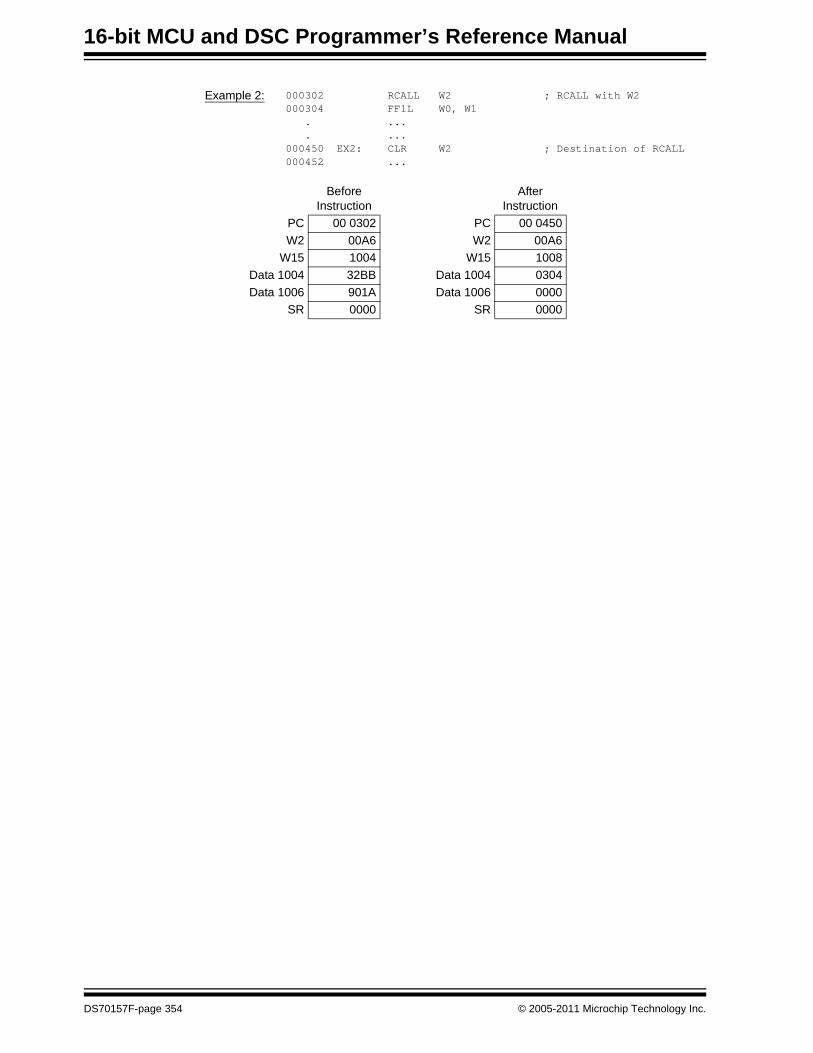
16-bit MCU and DSC Programmer’s Reference Manual
Example 2: 000302 RCALL W2000304 FF1L W0, W1 . ... . ...000450 EX2: CLR W2000452 ...
; RCALL with W2
; Destination of RCALL
Before Instruction
After Instruction
PC 00 0302 PC 00 0450W2 00A6 W2 00A6
W15 1004 W15 1008Data 1004 32BB Data 1004 0304Data 1006 901A Data 1006 0000
SR 0000 SR 0000
DS70157F-page 354 © 2005-2011 Microchip Technology Inc.

Section 5. Instruction DescriptionsInstruction
Descriptions
5
REPEAT Repeat Next Instruction ‘lit14 + 1’ Times
Implemented in: PIC24F PIC24H PIC24E dsPIC30F dsPIC33F dsPIC33E
X X X X
Syntax: {label:} REPEAT #lit14
Operands: lit14 ∈ [0 ... 16383]
Operation: (lit14) → RCOUNT(PC) + 2 → PCEnable Code Looping
Status Affected: RA
Encoding: 0000 1001 00kk kkkk kkkk kkkk
Description: Repeat the instruction immediately following the REPEAT instruction (lit14 + 1) times. The repeated instruction (or target instruction) is held in the instruction register for all iterations and is only fetched once.When this instruction executes, the RCOUNT register is loaded with the repeat count value specified in the instruction. RCOUNT is decremented with each execution of the target instruction. When RCOUNT equals zero, the target instruction is executed one more time, and then normal instruction execution continues with the instruction following the target instruction.The ‘k’ bits are an unsigned literal that specifies the loop count.Special Features, Restrictions:1. When the repeat literal is ‘0’, REPEAT has the effect of a NOP and
the RA bit is not set.2. The target REPEAT instruction cannot be:
• an instruction that changes program flow• a DO, DISI, LNK, MOV.D, PWRSAV, REPEAT or UNLK
instruction• a 2-word instruction
Unexpected results may occur if these target instructions are used.
Note: The REPEAT and target instruction are interruptible.
Words: 1
Cycles: 1
Example 1: 000452 REPEAT #9 ; Execute ADD 10 times000454 ADD [W0++], W1, [W2++] ; Vector update
Before Instruction
After Instruction
PC 00 0452 PC 00 0454RCOUNT 0000 RCOUNT 0009
SR 0000 SR 0010 (RA = 1)
© 2005-2011 Microchip Technology Inc. DS70157F-page 355

16-bit MCU and DSC Programmer’s Reference Manual
Example 2: 00089E REPEAT #0x3FF ; Execute CLR 1024 times0008A0 CLR [W6++] ; Clear the scratch space
Before Instruction
After Instruction
PC 00 089E PC 00 08A0RCOUNT 0000 RCOUNT 03FF
SR 0000 SR 0010 (RA = 1)
DS70157F-page 356 © 2005-2011 Microchip Technology Inc.

Section 5. Instruction DescriptionsInstruction
Descriptions
5
REPEAT Repeat Next Instruction ‘lit15 + 1’ Times
Implemented in: PIC24F PIC24H PIC24E dsPIC30F dsPIC33F dsPIC33E
X X
Syntax: {label:} REPEAT #lit15
Operands: lit15 ∈ [0 ... 32767]
Operation: (lit15) → RCOUNT(PC) + 2 → PCEnable Code Looping
Status Affected: RA
Encoding: 0000 1001 0kkk kkkk kkkk kkkk
Description: Repeat the instruction immediately following the REPEAT instruction (lit15 + 1) times. The repeated instruction (or target instruction) is held in the instruction register for all iterations and is only fetched once.When this instruction executes, the RCOUNT register is loaded with the repeat count value specified in the instruction. RCOUNT is decremented with each execution of the target instruction. When RCOUNT equals zero, the target instruction is executed one more time, and then normal instruction execution continues with the instruction following the target instruction.The ‘k’ bits are an unsigned literal that specifies the loop count.Special Features, Restrictions:1. When the repeat literal is ‘0’, REPEAT has the effect of a NOP and
the RA bit is not set.2. The target REPEAT instruction cannot be:
• an instruction that changes program flow• a DISI, LNK, MOV.D, PWRSAV, REPEAT or UNLK
instruction• a 2-word instruction
Unexpected results may occur if these target instructions are used.
Note: The REPEAT and target instruction are interruptible.
Words: 1
Cycles: 1
Example 1: 000452 REPEAT #9 ; Execute ADD 10 times000454 ADD [W0++], W1, [W2++] ; Vector update
Before Instruction
After Instruction
PC 00 0452 PC 00 0454RCOUNT 0000 RCOUNT 0009
SR 0000 SR 0010 (RA = 1)
© 2005-2011 Microchip Technology Inc. DS70157F-page 357

16-bit MCU and DSC Programmer’s Reference Manual
Example 2: 00089E REPEAT #0x3FF ; Execute CLR 1024 times0008A0 CLR [W6++] ; Clear the scratch space
Before Instruction
After Instruction
PC 00 089E PC 00 08A0RCOUNT 0000 RCOUNT 03FF
SR 0000 SR 0010 (RA = 1)
DS70157F-page 358 © 2005-2011 Microchip Technology Inc.

Section 5. Instruction DescriptionsInstruction
Descriptions
5
REPEAT Repeat Next Instruction Wn+1 Times
Implemented in: PIC24F PIC24H PIC24E dsPIC30F dsPIC33F dsPIC33E
X X X X
Syntax: {label:} REPEAT Wn
Operands: Wn ∈ [W0 ... W15]
Operation: (Wn<13:0>) → RCOUNT(PC) + 2 → PCEnable Code Looping
Status Affected: RA
Encoding: 0000 1001 1000 0000 0000 ssss
Description: Repeat the instruction immediately following the REPEAT instruction (Wn<13:0>) times. The instruction to be repeated (or target instruction) is held in the instruction register for all iterations and is only fetched once.
When this instruction executes, the RCOUNT register is loaded with the lower 14 bits of Wn. RCOUNT is decremented with each execution of the target instruction. When RCOUNT equals zero, the target instruction is executed one more time, and then normal instruction execution continues with the instruction following the target instruction.
The ‘s’ bits specify the Wn register that contains the repeat count.
Special Features, Restrictions:1. When (Wn) = 0, REPEAT has the effect of a NOP and the RA bit is
not set.2. The target REPEAT instruction cannot be:
• an instruction that changes program flow• a DO, DISI, LNK, MOV.D, PWRSAV, REPEAT or ULNK
instruction• a 2-word instruction
Unexpected results may occur if these target instructions are used.
Note: The REPEAT and target instruction are interruptible.
Words: 1
Cycles: 1
Example 1: 000A26 REPEAT W4 ; Execute COM (W4+1) times000A28 COM [W0++], [W2++] ; Vector complement
Before Instruction
After Instruction
PC 00 0A26 PC 00 0A28W4 0023 W4 0023
RCOUNT 0000 RCOUNT 0023SR 0000 SR 0010 (RA = 1)
© 2005-2011 Microchip Technology Inc. DS70157F-page 359

16-bit MCU and DSC Programmer’s Reference Manual
Example 2: 00089E REPEAT W10 ; Execute TBLRD (W10+1) times0008A0 TBLRDL [W2++], [W3++] ; Decrement (0x840)
Before Instruction
After Instruction
PC 00 089E PC 00 08A0W10 00FF W10 00FF
RCOUNT 0000 RCOUNT 00FFSR 0000 SR 0010 (RA = 1)
DS70157F-page 360 © 2005-2011 Microchip Technology Inc.

Section 5. Instruction DescriptionsInstruction
Descriptions
5
REPEAT Repeat Next Instruction Wn+1 Times
Implemented in: PIC24F PIC24H PIC24E dsPIC30F dsPIC33F dsPIC33E
X X
Syntax: {label:} REPEAT Wn
Operands: Wn ∈ [W0 ... W15]
Operation: (Wn) → RCOUNT(PC) + 2 → PCEnable Code Looping
Status Affected: RA
Encoding: 0000 1001 1000 0000 0000 ssss
Description: Repeat the instruction immediately following the REPEAT instruction (Wn) times. The instruction to be repeated (or target instruction) is held in the instruction register for all iterations and is only fetched once.
When this instruction executes, the RCOUNT register is loaded with Wn. RCOUNT is decremented with each execution of the target instruction. When RCOUNT equals zero, the target instruction is executed one more time, and then normal instruction execution continues with the instruction following the target instruction.
The ‘s’ bits specify the Wn register that contains the repeat count.
Special Features, Restrictions:1. When (Wn) = 0, REPEAT has the effect of a NOP and the RA bit is
not set.2. The target REPEAT instruction cannot be:
• an instruction that changes program flow• a DO, DISI, LNK, MOV.D, PWRSAV, REPEAT or ULNK
instruction• a 2-word instruction
Unexpected results may occur if these target instructions are used.
Note: The REPEAT and target instruction are interruptible.
Words: 1
Cycles: 1
Example 1: 000A26 REPEAT W4 ; Execute COM (W4+1) times000A28 COM [W0++], [W2++] ; Vector complement
Before Instruction
After Instruction
PC 00 0A26 PC 00 0A28W4 0023 W4 0023
RCOUNT 0000 RCOUNT 0023SR 0000 SR 0010 (RA = 1)
© 2005-2011 Microchip Technology Inc. DS70157F-page 361

16-bit MCU and DSC Programmer’s Reference Manual
Example 2: 00089E REPEAT W10 ; Execute TBLRD (W10+1) times0008A0 TBLRDL [W2++], [W3++] ; Decrement (0x840)
Before Instruction
After Instruction
PC 00 089E PC 00 08A0W10 00FF W10 00FF
RCOUNT 0000 RCOUNT 00FFSR 0000 SR 0010 (RA = 1)
DS70157F-page 362 © 2005-2011 Microchip Technology Inc.

Section 5. Instruction DescriptionsInstruction
Descriptions
5
RESET Reset
Implemented in: PIC24F PIC24H PIC24E dsPIC30F dsPIC33F dsPIC33E
X X X X X X
Syntax: {label:} RESET
Operands: None
Operation: Force all registers that are affected by a MCLR Reset to their Reset condition.1 → SWR (RCON<6>)0 → PC
Status Affected: OA, OB, OAB, SA, SB, SAB, DA, DC, IPL<2:0>, RA, N, OV, Z, C, SFA
Encoding: 1111 1110 0000 0000 0000 0000
Description: This instruction provides a way to execute a software Reset. All core and peripheral registers will take their power-on value. The PC will be set to ‘0’, the location of the RESET GOTO instruction. The SWR bit (RCON<6>), will be set to ‘1’ to indicate that the RESET instruction was executed.
Note: Refer to the specific device family reference manual for the power-on value of all registers.
Words: 1
Cycles: 1
© 2005-2011 Microchip Technology Inc. DS70157F-page 363

16-bit MCU and DSC Programmer’s Reference Manual
Example 1: 00202A RESET ; Execute software RESET on dsPIC33F
Before Instruction
After Instruction
PC 00 202A PC 00 0000W0 8901 W0 0000W1 08BB W1 0000W2 B87A W2 0000W3 872F W3 0000W4 C98A W4 0000W5 AAD4 W5 0000W6 981E W6 0000W7 1809 W7 0000W8 C341 W8 0000W9 90F4 W9 0000
W10 F409 W10 0000W11 1700 W11 0000W12 1008 W12 0000W13 6556 W13 0000W14 231D W14 0000W15 1704 W15 0800
SPLIM 1800 SPLIM 0000TBLPAG 007F TBLPAG 0000PSVPAG 0001 PSVPAG 0000
CORCON 00F0 CORCON 0020 (SATDW = 1)RCON 0000 RCON 0040 (SWR = 1)
SR 0021 (IPL, C = 1) SR 0000
DS70157F-page 364 © 2005-2011 Microchip Technology Inc.

Section 5. Instruction DescriptionsInstruction
Descriptions
5
RETFIE Return from Interrupt
Implemented in: PIC24F PIC24H PIC24E dsPIC30F dsPIC33F dsPIC33E
X X X X
Syntax: {label:} RETFIE
Operands: None
Operation: (W15) - 2 → W15(TOS<15:8>) → (SR<7:0>)(TOS<7>) → (IPL3, CORCON<3>)(TOS<6:0>) → (PC<22:16>)(W15) - 2 → W15(TOS<15:0>) → (PC<15:0>)NOP → Instruction Register
Status Affected: IPL<3:0>, RA, N, OV, Z, C
Encoding: 0000 0110 0100 0000 0000 0000
Description: Return from Interrupt Service Routine. The stack is POPped, which loads the low byte of the STATUS register, IPL<3> (CORCON<3>) and the Most Significant Byte of the PC. The stack is POPped again, which loads the lower 16 bits of the PC.
Note 1: Restoring IPL<3> and the low byte of the STATUS register restores the Interrupt Priority Level to the level before the execution was processed.
2: Before RETFIE is executed, the appropriate interrupt flag must be cleared in software to avoid recursive interrupts.
Words: 1
Cycles: 3 (2 if exception pending)
Example 1: 000A26 RETFIE ; Return from ISR
Before Instruction
After Instruction
PC 00 0A26 PC 01 0230W15 0834 W15 0830
Data 0830 0230 Data 0830 0230Data 0832 8101 Data 0832 8101CORCON 0001 CORCON 0001
SR 0000 SR 0081 (IPL = 4, C = 1)
Example 2: 008050 RETFIE ; Return from ISR
Before Instruction
After Instruction
PC 00 8050 PC 00 7008W15 0926 W15 0922
Data 0922 7008 Data 0922 7008Data 0924 0300 Data 0924 0300CORCON 0000 CORCON 0000
SR 0000 SR 0003 (Z, C = 1)
© 2005-2011 Microchip Technology Inc. DS70157F-page 365
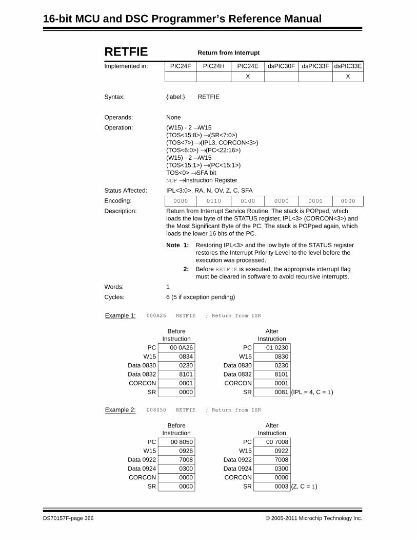
16-bit MCU and DSC Programmer’s Reference Manual
RETFIE Return from Interrupt
Implemented in: PIC24F PIC24H PIC24E dsPIC30F dsPIC33F dsPIC33E
X X
Syntax: {label:} RETFIE
Operands: None
Operation: (W15) - 2 → W15(TOS<15:8>) → (SR<7:0>)(TOS<7>) → (IPL3, CORCON<3>)(TOS<6:0>) → (PC<22:16>)(W15) - 2 → W15(TOS<15:1>) → (PC<15:1>)TOS<0> → SFA bitNOP → Instruction Register
Status Affected: IPL<3:0>, RA, N, OV, Z, C, SFA
Encoding: 0000 0110 0100 0000 0000 0000
Description: Return from Interrupt Service Routine. The stack is POPped, which loads the low byte of the STATUS register, IPL<3> (CORCON<3>) and the Most Significant Byte of the PC. The stack is POPped again, which loads the lower 16 bits of the PC.
Note 1: Restoring IPL<3> and the low byte of the STATUS register restores the Interrupt Priority Level to the level before the execution was processed.
2: Before RETFIE is executed, the appropriate interrupt flag must be cleared in software to avoid recursive interrupts.
Words: 1
Cycles: 6 (5 if exception pending)
Example 1: 000A26 RETFIE ; Return from ISR
Before Instruction
After Instruction
PC 00 0A26 PC 01 0230W15 0834 W15 0830
Data 0830 0230 Data 0830 0230Data 0832 8101 Data 0832 8101CORCON 0001 CORCON 0001
SR 0000 SR 0081 (IPL = 4, C = 1)
Example 2: 008050 RETFIE ; Return from ISR
Before Instruction
After Instruction
PC 00 8050 PC 00 7008W15 0926 W15 0922
Data 0922 7008 Data 0922 7008Data 0924 0300 Data 0924 0300CORCON 0000 CORCON 0000
SR 0000 SR 0003 (Z, C = 1)
DS70157F-page 366 © 2005-2011 Microchip Technology Inc.

Section 5. Instruction DescriptionsInstruction
Descriptions
5
RETLW Return with Literal in Wn
Implemented in: PIC24F PIC24H PIC24E dsPIC30F dsPIC33F dsPIC33EX X X X
Syntax: {label:} RETLW{.B} #lit10, Wn
Operands: lit10 ∈ [0 ... 255] for byte operationlit10 ∈ [0 ... 1023] for word operationWn ∈ [W0 ... W15]
Operation: (W15) – 2 → W15TOS<15:8> → SR<7:0>TOS<7:0> → IPL<3> : PC<22:16>(W15) – 2 → W15(TOS) → (PC<15:0>)lit10 → WnNOP → Instruction register
Status Affected: NoneEncoding: 0000 0101 0Bkk kkkk kkkk dddd
Description: Return from subroutine with the specified, unsigned 10-bit literal stored in Wn. The software stack is POPped twice to restore the PC and the signed literal is stored in Wn. Since two POPs are made, the Stack Pointer (W15) is decremented by 4.
The ‘B’ bit selects byte or word operation (‘0’ for word, ‘1’ for byte).The ‘k’ bits specify the value of the literal.The ‘d’ bits select the destination register.
Note 1: The extension .B in the instruction denotes a byte operation rather than a word operation. You may use a .W extension to denote a word operation, but it is not required.
2: For byte operations, the literal must be specified as an unsigned value [0:255]. See Section 4.6 “Using 10-bit Lit-eral Operands” for information on using 10-bit literal operands in Byte mode.
Words: 1Cycles: 3 (2 if exception pending)
Example 1: 000440 RETLW.B #0xA, W0 ; Return with 0xA in W0
Before Instruction
After Instruction
PC 00 0440 PC 00 7006W0 9846 W0 980A
W15 1988 W15 1984Data 1984 7006 Data 1984 7006Data 1986 0000 Data 1986 0000
SR 0000 SR 0000
© 2005-2011 Microchip Technology Inc. DS70157F-page 367

16-bit MCU and DSC Programmer’s Reference Manual
Example 2: 00050A RETLW #0x230, W2 ; Return with 0x230 in W2
Before Instruction
After Instruction
PC 00 050A PC 01 7008W2 0993 W2 0230
W15 1200 W15 11FCData 11FC 7008 Data 11FC 7008Data 11FE 0001 Data 11FE 0001
SR 0000 SR 0000
DS70157F-page 368 © 2005-2011 Microchip Technology Inc.

Section 5. Instruction DescriptionsInstruction
Descriptions
5
RETLW Return with Literal in Wn
Implemented in: PIC24F PIC24H PIC24E dsPIC30F dsPIC33F dsPIC33EX X
Syntax: {label:} RETLW{.B} #lit10, Wn
Operands: lit10 ∈ [0 ... 255] for byte operationlit10 ∈ [0 ... 1023] for word operationWn ∈ [W0 ... W15]
Operation: (W15) – 2 → W15TOS<15:8> → SR<7:0>TOS<7:0> → IPL<3>: PC<22:16>(W15) – 2 → W15(TOS<15:1>) → (PC<15:1>)TOS<0> → SFA bitlit10 → WnNOP → Instruction register
Status Affected: SFAEncoding: 0000 0101 0Bkk kkkk kkkk dddd
Description: Return from subroutine with the specified, unsigned 10-bit literal stored in Wn. The software stack is POPped twice to restore the PC and the signed literal is stored in Wn. Since two POPs are made, the Stack Pointer (W15) is decremented by 4.
The ‘B’ bit selects byte or word operation (‘0’ for word, ‘1’ for byte).The ‘k’ bits specify the value of the literal.The ‘d’ bits select the destination register.
Note 1: The extension .B in the instruction denotes a byte operation rather than a word operation. You may use a .W extension to denote a word operation, but it is not required.
2: For byte operations, the literal must be specified as an unsigned value [0:255]. See Section 4.6 “Using 10-bit Lit-eral Operands” for information on using 10-bit literal operands in Byte mode.
Words: 1Cycles: 6 (5 if exception pending)
Example 1: 000440 RETLW.B #0xA, W0 ; Return with 0xA in W0
Before Instruction
After Instruction
PC 00 0440 PC 00 7006W0 9846 W0 980A
W15 1988 W15 1984Data 1984 7006 Data 1984 7006Data 1986 0000 Data 1986 0000
SR 0000 SR 0000
© 2005-2011 Microchip Technology Inc. DS70157F-page 369

16-bit MCU and DSC Programmer’s Reference Manual
Example 2: 00050A RETLW #0x230, W2 ; Return with 0x230 in W2
Before Instruction
After Instruction
PC 00 050A PC 01 7008W2 0993 W2 0230
W15 1200 W15 11FCData 11FC 7008 Data 11FC 7008Data 11FE 0001 Data 11FE 0001
SR 0000 SR 0000
DS70157F-page 370 © 2005-2011 Microchip Technology Inc.

Section 5. Instruction DescriptionsInstruction
Descriptions
5
RETURN Return
Implemented in: PIC24F PIC24H PIC24E dsPIC30F dsPIC33F dsPIC33E
X X X X
Syntax: {label:} RETURN
Operands: None
Operation: (W15) – 2 → W15(TOS) → (PC<22:16>)(W15) – 2 → W15(TOS) → (PC<15:0>)NOP → Instruction Register
Status Affected: None
Encoding: 0000 0110 0000 0000 0000 0000
Description: Return from subroutine. The software stack is POPped twice to restore the PC. Since two POPs are made, the Stack Pointer (W15) is decremented by 4.
Words: 1
Cycles: 3 (2 if exception pending)
Example 1: 001A06 RETURN ; Return from subroutine
Before Instruction
After Instruction
PC 00 1A06 PC 01 0004W15 1248 W15 1244
Data 1244 0004 Data 1244 0004Data 1246 0001 Data 1246 0001
SR 0000 SR 0000
Example 2: 005404 RETURN ; Return from subroutine
Before Instruction
After Instruction
PC 00 5404 PC 00 0966W15 090A W15 0906
Data 0906 0966 Data 0906 0966Data 0908 0000 Data 0908 0000
SR 0000 SR 0000
© 2005-2011 Microchip Technology Inc. DS70157F-page 371

16-bit MCU and DSC Programmer’s Reference Manual
RETURN Return
Implemented in: PIC24F PIC24H PIC24E dsPIC30F dsPIC33F dsPIC33E
X X
Syntax: {label:} RETURN
Operands: None
Operation: (W15) – 2 → W15(TOS) → (PC<22:16>)(W15) – 2 → W15(TOS<15:1) → (PC<15:1>)TOS<0> → SFA bitNOP → Instruction Register
Status Affected: SFA
Encoding: 0000 0110 0000 0000 0000 0000
Description: Return from subroutine. The software stack is POPped twice to restore the PC. Since two POPs are made, the Stack Pointer (W15) is decremented by 4.
Words: 1
Cycles: 6 (5 if exception pending)
Example 1: 001A06 RETURN ; Return from subroutine
Before Instruction
After Instruction
PC 00 1A06 PC 01 0004W15 1248 W15 1244
Data 1244 0004 Data 1244 0004Data 1246 0001 Data 1246 0001
SR 0000 SR 0000
Example 2: 005404 RETURN ; Return from subroutine
Before Instruction
After Instruction
PC 00 5404 PC 00 0966W15 090A W15 0906
Data 0906 0966 Data 0906 0966Data 0908 0000 Data 0908 0000
SR 0000 SR 0000
DS70157F-page 372 © 2005-2011 Microchip Technology Inc.

Section 5. Instruction DescriptionsInstruction
Descriptions
5
RLC Rotate Left f through Carry
Implemented in: PIC24F PIC24H PIC24E dsPIC30F dsPIC33F dsPIC33E
X X X X X X
Syntax: {label:} RLC{.B} f {,WREG}
Operands: f ∈ [0 ... 8191]
Operation: For byte operation: (C) → Dest<0> (f<6:0>) → Dest<7:1> (f<7>) → CFor word operation: (C) → Dest<0> (f<14:0>) → Dest<15:1> (f<15>) → C
Status Affected: N, Z, C
Encoding: 1101 0110 1BDf ffff ffff ffff
Description: Rotate the contents of the file register f one bit to the left through the Carry flag and place the result in the destination register. The Carry flag of the STATUS Register is shifted into the Least Significant bit of the destination, and it is then overwritten with the Most Significant bit of Ws.
The optional WREG operand determines the destination register. If WREG is specified, the result is stored in WREG. If WREG is not specified, the result is stored in the file register.
The ‘B’ bit selects byte or word operation (‘0’ for word, ‘1’ for byte).The ‘D’ bit selects the destination (‘0’ for f, ‘1’ for WREG).The ‘f’ bits select the address of the file register.
Note 1: The extension .B in the instruction denotes a byte operation rather than a word operation. You may use a .W extension to denote a word operation, but it is not required.
2: The WREG is set to working register W0.
Words: 1
Cycles: 1
C
Example 1: RLC.B 0x1233 ; Rotate Left w/ C (0x1233) (Byte mode)
Before Instruction
After Instruction
Data 1232 E807 Data 1232 D007SR 0000 SR 0009 (N, C = 1)
© 2005-2011 Microchip Technology Inc. DS70157F-page 373

16-bit MCU and DSC Programmer’s Reference Manual
Example 2: RLC 0x820, WREG ; Rotate Left w/ C (0x820) (Word mode) ; Store result in WREG
Before Instruction
After Instruction
WREG (W0) 5601 WREG (W0) 42DDData 0820 216E Data 0820 216E
SR 0001 (C = 1) SR 0000 (C = 0)
DS70157F-page 374 © 2005-2011 Microchip Technology Inc.

Section 5. Instruction DescriptionsInstruction
Descriptions
5
RLC Rotate Left Ws through Carry
Implemented in: PIC24F PIC24H PIC24E dsPIC30F dsPIC33F dsPIC33E
X X X X X X
Syntax: {label:} RLC{.B} Ws, Wd
[Ws], [Wd]
[Ws++], [Wd++]
[Ws--], [Wd--]
[++Ws], [++Wd]
[--Ws], [--Wd]
Operands: Ws ∈ [W0 ... W15]Wd ∈ [W0 ... W15]
Operation: For byte operation: (C) → Wd<0> (Ws<6:0>) → Wd<7:1> (Ws<7>) → CFor word operation: (C) → Wd<0> (Ws<14:0>) → Wd<15:1> (Ws<15>) → C
Status Affected: N, Z, C
Encoding: 1101 0010 1Bqq qddd dppp ssss
Description: Rotate the contents of the source register Ws one bit to the left through the Carry flag and place the result in the destination register Wd. The Carry flag of the STATUS register is shifted into the Least Significant bit of Wd, and it is then overwritten with the Most Significant bit of Ws. Either register direct or indirect addressing may be used for Ws and Wd.
The ‘B’ bit selects byte or word operation (‘0’ for word, ‘1’ for byte).The ‘q’ bits select the destination Address mode.The ‘d’ bits select the destination register.The ‘p’ bits select the source Address mode.The ‘s’ bits select the source register.
Note: The extension .B in the instruction denotes a byte operation rather than a word operation. You may use a .W extension to denote a word operation, but it is not required.
Words: 1
Cycles: 1
C
Example 1: RLC.B W0, W3 ; Rotate Left w/ C (W0) (Byte mode) ; Store the result in W3
Before Instruction
After Instruction
W0 9976 W0 9976W3 5879 W3 58EDSR 0001 (C = 1) SR 0009 (N = 1)
© 2005-2011 Microchip Technology Inc. DS70157F-page 375

16-bit MCU and DSC Programmer’s Reference Manual
Example 2: RLC [W2++], [W8] ; Rotate Left w/ C [W2] (Word mode) ; Post-increment W2 ; Store result in [W8]
Before Instruction
After Instruction
W2 2008 W2 200AW8 094E W8 094E
Data 094E 3689 Data 094E 8082Data 2008 C041 Data 2008 C041
SR 0001 (C = 1) SR 0009 (N, C = 1)
DS70157F-page 376 © 2005-2011 Microchip Technology Inc.

Section 5. Instruction DescriptionsInstruction
Descriptions
5
RLNC Rotate Left f without Carry
Implemented in: PIC24F PIC24H PIC24E dsPIC30F dsPIC33F dsPIC33E
X X X X X X
Syntax: {label:} RLNC{.B} f {,WREG}
Operands: f ∈ [0 ... 8191]
Operation: For byte operation: (f<6:0>) → Dest<7:1> (f<7>) → Dest<0>For word operation: (f<14:0>) → Dest<15:1> (f<15>) → Dest<0>
Status Affected: N, Z
Encoding: 1101 0110 0BDf ffff ffff ffff
Description: Rotate the contents of the file register f one bit to the left and place the result in the destination register. The Most Significant bit of f is stored in the Least Significant bit of the destination, and the Carry flag is not affected.
The optional WREG operand determines the destination register. If WREG is specified, the result is stored in WREG. If WREG is not specified, the result is stored in the file register.
The ‘B’ bit selects byte or word operation (‘0’ for word, ‘1’ for byte).The ‘D’ bit selects the destination (‘0’ for WREG, ‘1’ for file register).The ‘f’ bits select the address of the file register.
Note 1: The extension .B in the instruction denotes a byte operation rather than a word operation. You may use a .W extension to denote a word operation, but it is not required.
2: The WREG is set to working register W0.
Words: 1
Cycles: 1(1)
Note 1: In dsPIC33E and PIC24E devices, the listed cycle count does not apply to read and read-modify-write operations on non-CPU Special Function Registers. For more details, see Note 3 in Section 3.2.1 “Multi-Cycle Instructions”.
© 2005-2011 Microchip Technology Inc. DS70157F-page 377

16-bit MCU and DSC Programmer’s Reference Manual
Example 1: RLNC.B 0x1233 ; Rotate Left (0x1233) (Byte mode)
Before Instruction
After Instruction
Data 1232 E807 Data 1233 D107SR 0000 SR 0008 (N = 1)
Example 2: RLNC 0x820, WREG ; Rotate Left (0x820) (Word mode) ; Store result in WREG
Before Instruction
After Instruction
WREG (W0) 5601 WREG (W0) 42DCData 0820 216E Data 0820 216E
SR 0001 (C = 1) SR 0000 (C = 0)
DS70157F-page 378 © 2005-2011 Microchip Technology Inc.

Section 5. Instruction DescriptionsInstruction
Descriptions
5
RLNC Rotate Left Ws without Carry
Implemented in: PIC24F PIC24H PIC24E dsPIC30F dsPIC33F dsPIC33E
X X X X X X
Syntax: {label:} RLNC{.B} Ws, Wd
[Ws], [Wd]
[Ws++], [Wd++]
[Ws--], [Wd--]
[++Ws], [++Wd]
[--Ws], [--Wd]
Operands: Ws ∈ [W0 ... W15]Wd ∈ [W0 ... W15]
Operation: For byte operation: (Ws<6:0>) → Wd<7:1> (Ws<7>) → Wd<0>For word operation: (Ws<14:0>) → Wd<15:1> (Ws<15>) → Wd<0>
Status Affected: N, Z
Encoding: 1101 0010 0Bqq qddd dppp ssss
Description: Rotate the contents of the source register Ws one bit to the left and place the result in the destination register Wd. The Most Significant bit of Ws is stored in the Least Significant bit of Wd, and the Carry flag is not affected. Either register direct or indirect addressing may be used for Ws and Wd.
The ‘B’ bit selects byte or word operation (‘0’ for byte, ‘1’ for word).The ‘q’ bits select the destination Address mode.The ‘d’ bits select the destination register.The ‘p’ bits select the source Address mode.The ‘s’ bits select the source register.
Note: The extension .B in the instruction denotes a byte operation rather than a word operation. You may use a .W extension to denote a word operation, but it is not required.
Words: 1
Cycles: 1(1)
Note 1: In dsPIC33E and PIC24E devices, the listed cycle count does not apply to read and read-modify-write operations on non-CPU Special Function Registers. For more details, see Note 3 in Section 3.2.1 “Multi-Cycle Instructions”.
© 2005-2011 Microchip Technology Inc. DS70157F-page 379

16-bit MCU and DSC Programmer’s Reference Manual
Example 1: RLNC.B W0, W3 ; Rotate Left (W0) (Byte mode) ; Store the result in W3
Before Instruction
After Instruction
W0 9976 W0 9976W3 5879 W3 58ECSR 0001 (C = 1) SR 0009 (N, C = 1)
Example 2: RLNC [W2++], [W8] ; Rotate Left [W2] (Word mode) ; Post-increment W2 ; Store result in [W8]
Before Instruction
After Instruction
W2 2008 W2 200AW8 094E W8 094E
Data 094E 3689 Data 094E 8083Data 2008 C041 Data 2008 C041
SR 0001 (C = 1) SR 0009 (N, C = 1)
DS70157F-page 380 © 2005-2011 Microchip Technology Inc.

Section 5. Instruction DescriptionsInstruction
Descriptions
5
RRC Rotate Right f through Carry
Implemented in: PIC24F PIC24H PIC24E dsPIC30F dsPIC33F dsPIC33EX X X X X X
Syntax: {label:} RRC{.B} f {,WREG}
Operands: f ∈ [0 ... 8191]Operation: For byte operation:
(C) → Dest<7> (f<7:1>) → Dest<6:0> (f<0>) → CFor word operation: (C) → Dest<15> (f<15:1>) → Dest<14:0> (f<0>) → C
Status Affected: N, Z, CEncoding: 1101 0111 1BDf ffff ffff ffff
Description: Rotate the contents of the file register f one bit to the right through the Carry flag and place the result in the destination register. The Carry flag of the STATUS Register is shifted into the Most Significant bit of the destination, and it is then overwritten with the Least Significant bit of Ws.
The optional WREG operand determines the destination register. If WREG is specified, the result is stored in WREG. If WREG is not specified, the result is stored in the file register.
The ‘B’ bit selects byte or word operation (‘0’ for byte, ‘1’ for word).The ‘D’ bit selects the destination (‘0’ for WREG, ‘1’ for file register).The ‘f’ bits select the address of the file register.
Note 1: The extension .B in the instruction denotes a byte operation rather than a word operation. You may use a .W extension to denote a word operation, but it is not required.
2: The WREG is set to working register W0.Words: 1Cycles: 1(1)
Note 1: In dsPIC33E and PIC24E devices, the listed cycle count does not apply to read and read-modify-write operations on non-CPU Special Function Registers. For more details, see Note 3 in Section 3.2.1 “Multi-Cycle Instructions”.
C
Example 1: RRC.B 0x1233 ; Rotate Right w/ C (0x1233) (Byte mode)
Before Instruction
After Instruction
Data 1232 E807 Data 1232 7407SR 0000 SR 0000
© 2005-2011 Microchip Technology Inc. DS70157F-page 381

16-bit MCU and DSC Programmer’s Reference Manual
Example 2: RRC 0x820, WREG ; Rotate Right w/ C (0x820) (Word mode) ; Store result in WREG
Before Instruction
After Instruction
WREG (W0) 5601 WREG (W0) 90B7Data 0820 216E Data 0820 216E
SR 0001 (C = 1) SR 0008 (N = 1)
DS70157F-page 382 © 2005-2011 Microchip Technology Inc.
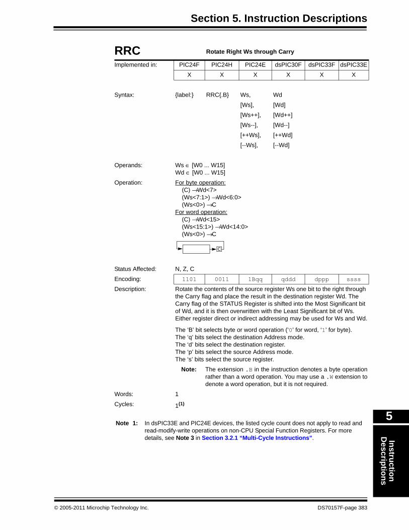
Section 5. Instruction DescriptionsInstruction
Descriptions
5
RRC Rotate Right Ws through Carry
Implemented in: PIC24F PIC24H PIC24E dsPIC30F dsPIC33F dsPIC33E
X X X X X X
Syntax: {label:} RRC{.B} Ws, Wd
[Ws], [Wd]
[Ws++], [Wd++]
[Ws--], [Wd--]
[++Ws], [++Wd]
[--Ws], [--Wd]
Operands: Ws ∈ [W0 ... W15]Wd ∈ [W0 ... W15]
Operation: For byte operation: (C) → Wd<7> (Ws<7:1>) → Wd<6:0> (Ws<0>) → CFor word operation: (C) → Wd<15> (Ws<15:1>) → Wd<14:0> (Ws<0>) → C
Status Affected: N, Z, C
Encoding: 1101 0011 1Bqq qddd dppp ssss
Description: Rotate the contents of the source register Ws one bit to the right through the Carry flag and place the result in the destination register Wd. The Carry flag of the STATUS Register is shifted into the Most Significant bit of Wd, and it is then overwritten with the Least Significant bit of Ws. Either register direct or indirect addressing may be used for Ws and Wd.
The ‘B’ bit selects byte or word operation (‘0’ for word, ‘1’ for byte).The ‘q’ bits select the destination Address mode.The ‘d’ bits select the destination register.The ‘p’ bits select the source Address mode.The ‘s’ bits select the source register.
Note: The extension .B in the instruction denotes a byte operation rather than a word operation. You may use a .W extension to denote a word operation, but it is not required.
Words: 1
Cycles: 1(1)
Note 1: In dsPIC33E and PIC24E devices, the listed cycle count does not apply to read and read-modify-write operations on non-CPU Special Function Registers. For more details, see Note 3 in Section 3.2.1 “Multi-Cycle Instructions”.
C
© 2005-2011 Microchip Technology Inc. DS70157F-page 383

16-bit MCU and DSC Programmer’s Reference Manual
Example 1: RRC.B W0, W3 ; Rotate Right w/ C (W0) (Byte mode) ; Store the result in W3
Before Instruction
After Instruction
W0 9976 W0 9976W3 5879 W3 58BBSR 0001 (C = 1) SR 0008 (N = 1)
Example 2: RRC [W2++], [W8] ; Rotate Right w/ C [W2] (Word mode) ; Post-increment W2 ; Store result in [W8]
Before Instruction
After Instruction
W2 2008 W2 200AW8 094E W8 094E
Data 094E 3689 Data 094E E020Data 2008 C041 Data 2008 C041
SR 0001 (C = 1) SR 0009 (N, C = 1)
DS70157F-page 384 © 2005-2011 Microchip Technology Inc.

Section 5. Instruction DescriptionsInstruction
Descriptions
5
RRNC Rotate Right f without Carry
Implemented in: PIC24F PIC24H PIC24E dsPIC30F dsPIC33F dsPIC33E
X X X X X X
Syntax: {label:} RRNC{.B} f {,WREG}
Operands: f ∈ [0 ... 8191]
Operation: For byte operation: (f<7:1>) → Dest<6:0> (f<0>) → Dest<7>For word operation: (f<15:1>) → Dest<14:0> (f<0>) → Dest<15>
Status Affected: N, Z
Encoding: 1101 0111 0BDf ffff ffff ffff
Description: Rotate the contents of the file register f one bit to the right and place the result in the destination register. The Least Significant bit of f is stored in the Most Significant bit of the destination, and the Carry flag is not affected.
The optional WREG operand determines the destination register. If WREG is specified, the result is stored in WREG. If WREG is not specified, the result is stored in the file register.
The ‘B’ bit selects byte or word operation (‘0’ for word, ‘1’ for byte).The ‘D’ bit selects the destination (‘0’ for WREG, ‘1’ for file register).The ‘f’ bits select the address of the file register.
Note 1: The extension .B in the instruction denotes a byte operation rather than a word operation. You may use a .W extension to denote a word operation, but it is not required.
2: The WREG is set to working register W0.
Words: 1
Cycles: 1(1)
Note 1: In dsPIC33E and PIC24E devices, the listed cycle count does not apply to read and read-modify-write operations on non-CPU Special Function Registers. For more details, see Note 3 in Section 3.2.1 “Multi-Cycle Instructions”.
© 2005-2011 Microchip Technology Inc. DS70157F-page 385

16-bit MCU and DSC Programmer’s Reference Manual
Example 1: RRNC.B 0x1233 ; Rotate Right (0x1233) (Byte mode)
Before Instruction
After Instruction
Data 1232 E807 Data 1232 7407SR 0000 SR 0000
Example 2: RRNC 0x820, WREG ; Rotate Right (0x820) (Word mode) ; Store result in WREG
Before Instruction
After Instruction
WREG (W0) 5601 WREG (W0) 10B7Data 0820 216E Data 0820 216E
SR 0001 (C = 1) SR 0001 (C = 1)
DS70157F-page 386 © 2005-2011 Microchip Technology Inc.

Section 5. Instruction DescriptionsInstruction
Descriptions
5
RRNC Rotate Right Ws without Carry
Implemented in: PIC24F PIC24H PIC24E dsPIC30F dsPIC33F dsPIC33E
X X X X X X
Syntax: {label:} RRNC{.B} Ws, Wd
[Ws], [Wd]
[Ws++], [Wd++]
[Ws--], [Wd--]
[++Ws], [++Wd]
[--Ws], [--Wd]
Operands: Ws ∈ [W0 ... W15]Wd ∈ [W0 ... W15]
Operation: For byte operation: (Ws<7:1>) → Wd<6:0> (Ws<0>) → Wd<7>For word operation: (Ws<15:1>) → Wd<14:0> (Ws<0>) → Wd<15>
Status Affected: N, Z
Encoding: 1101 0011 0Bqq qddd dppp ssss
Description: Rotate the contents of the source register Ws one bit to the right and place the result in the destination register Wd. The Least Significant bit of Ws is stored in the Most Significant bit of Wd, and the Carry flag is not affected. Either register direct or indirect addressing may be used for Ws and Wd.
The ‘B’ bit selects byte or word operation (‘0’ for word, ‘1’ for byte).The ‘q’ bits select the destination Address mode.The ‘d’ bits select the destination register.The ‘p’ bits select the source Address mode.The ‘s’ bits select the source register.
Note: The extension .B in the instruction denotes a byte operation rather than a word operation. You may use a .W extension to denote a word operation, but it is not required.
Words: 1
Cycles: 1(1)
Note 1: In dsPIC33E and PIC24E devices, the listed cycle count does not apply to read and read-modify-write operations on non-CPU Special Function Registers. For more details, see Note 3 in Section 3.2.1 “Multi-Cycle Instructions”.
© 2005-2011 Microchip Technology Inc. DS70157F-page 387

16-bit MCU and DSC Programmer’s Reference Manual
Example 1: RRNC.B W0, W3 ; Rotate Right (W0) (Byte mode) ; Store the result in W3
Before Instruction
After Instruction
W0 9976 W0 9976W3 5879 W3 583BSR 0001 (C = 1) SR 0001 (C = 1)
Example 2: RRNC [W2++], [W8] ; Rotate Right [W2] (Word mode) ; Post-increment W2 ; Store result in [W8]
Before Instruction
After Instruction
W2 2008 W2 200AW8 094E W8 094E
Data 094E 3689 Data 094E E020Data 2008 C041 Data 2008 C041
SR 0000 SR 0008 (N = 1)
DS70157F-page 388 © 2005-2011 Microchip Technology Inc.

Section 5. Instruction DescriptionsInstruction
Descriptions
5
SAC Store Accumulator
Implemented in: PIC24F PIC24H PIC24E dsPIC30F dsPIC33F dsPIC33E
X X X
Syntax: {label:} SAC Acc, {#Slit4,} Wd
[Wd]
[Wd++]
[Wd--]
[--Wd]
[++Wd]
[Wd + Wb]
Operands: Acc ∈ [A,B] Slit4 ∈ [-8 ... +7]Wb, Wd ∈ [W0 ... W15]
Operation: ShiftSlit4(Acc) (optional)(Acc[31:16]) → Wd
Status Affected: None
Encoding: 1100 1100 Awww wrrr rhhh dddd
Description: Perform an optional, signed 4-bit shift of the specified accumulator, then store the shifted contents of ACCxH (Acc[31:16]) to Wd. The shift range is -8:7, where a negative operand indicates an arithmetic left shift and a positive operand indicates an arithmetic right shift. Either register direct or indirect addressing may be used for Wd.
The ‘A’ bit specifies the source accumulator. The ‘w’ bits specify the offset register Wb.The ‘r’ bits encode the optional accumulator pre-shift.The ‘h’ bits select the destination Address mode.The ‘d’ bits specify the destination register Wd.
Note 1: This instruction does not modify the contents of Acc.2: This instruction stores the truncated contents of Acc. The
instruction SAC.R may be used to store the rounded accumulator contents.
3: If Data Write saturation is enabled (SATDW, CORCON<5>, = 1), the value stored to Wd is subject to saturation after the optional shift is performed.
Words: 1
Cycles: 1
Example 1: SAC A, #4, W5 ; Right shift ACCA by 4 ; Store result to W5 ; CORCON = 0x0010 (SATDW = 1)
Before Instruction
After Instruction
W5 B900 W5 0120ACCA 00 120F FF00 ACCA 00 120F FF00
CORCON 0010 CORCON 0010SR 0000 SR 0000
© 2005-2011 Microchip Technology Inc. DS70157F-page 389

16-bit MCU and DSC Programmer’s Reference Manual
Example 2: SAC B, #-4, [W5++] ; Left shift ACCB by 4 ; Store result to [W5], Post-increment W5; CORCON = 0x0010 (SATDW = 1)
Before Instruction
After Instruction
W5 2000 W5 2002ACCB FF C891 8F4C ACCB FF C891 1F4C
Data 2000 5BBE Data 2000 8000CORCON 0010 CORCON 0010
SR 0000 SR 0000
DS70157F-page 390 © 2005-2011 Microchip Technology Inc.

Section 5. Instruction DescriptionsInstruction
Descriptions
5
SAC.R Store Rounded Accumulator
Implemented in: PIC24F PIC24H PIC24E dsPIC30F dsPIC33F dsPIC33E
X X X
Syntax: {label:} SAC.R Acc, {#Slit4,} Wd
[Wd]
[Wd++]
[Wd--]
[--Wd]
[++Wd]
[Wd + Wb]
Operands: Acc ∈ [A,B] Slit4 ∈ [-8 ... +7]Wb ∈ [W0 ... W15]Wd ∈ [W0 ... W15]
Operation: ShiftSlit4(Acc) (optional)Round(Acc)(Acc[31:16]) → Wd
Status Affected: None
Encoding: 1100 1101 Awww wrrr rhhh dddd
Description: Perform an optional, signed 4-bit shift of the specified accumulator, then store the rounded contents of ACCxH (Acc[31:16]) to Wd. The shift range is -8:7, where a negative operand indicates an arithmetic left shift and a positive operand indicates an arithmetic right shift. The Rounding mode (Conventional or Convergent) is set by the RND bit, CORCON<1>. Either register direct or indirect addressing may be used for Wd.
The ‘A’ bit specifies the source accumulator. The ‘w’ bits specify the offset register Wb.The ‘r’ bits encode the optional accumulator pre-shift.The ‘h’ bits select the destination Address mode.The ‘d’ bits specify the destination register Wd.
Note 1: This instruction does not modify the contents of the Acc.2: This instruction stores the rounded contents of Acc. The
instruction SAC may be used to store the truncated accumulator contents.
3: If Data Write saturation is enabled (SATDW, CORCON<5>, = 1), the value stored to Wd is subject to saturation after the optional shift is performed.
Words: 1
Cycles: 1
© 2005-2011 Microchip Technology Inc. DS70157F-page 391

16-bit MCU and DSC Programmer’s Reference Manual
Example 1: SAC.R A, #4, W5 ; Right shift ACCA by 4 ; Store rounded result to W5 ; CORCON = 0x0010 (SATDW = 1)
Before Instruction
After Instruction
W5 B900 W5 0121ACCA 00 120F FF00 ACCA 00 120F FF00
CORCON 0010 CORCON 0010SR 0000 SR 0000
Example 2: SAC.R B, #-4, [W5++]; Left shift ACCB by 4 ; Store rounded result to [W5], Post-increment W5; CORCON = 0x0010 (SATDW = 1)
Before Instruction
After Instruction
W5 2000 W5 2002ACCB FF F891 8F4C ACCB FF F891 8F4C
Data 2000 5BBE Data 2000 8919CORCON 0010 CORCON 0010
SR 0000 SR 0000
DS70157F-page 392 © 2005-2011 Microchip Technology Inc.

Section 5. Instruction DescriptionsInstruction
Descriptions
5
SE Sign-Extend Ws
Implemented in: PIC24F PIC24H PIC24E dsPIC30F dsPIC33F dsPIC33EX X X X X X
Syntax: {label:} SE Ws, Wnd[Ws],[Ws++],[Ws--],[++Ws],[--Ws],
Operands: Ws ∈ [W0 ... W15]Wnd ∈ [W0 ... W15]
Operation: Ws<7:0> → Wnd<7:0>If (Ws<7> = 1): 0xFF → Wnd<15:8>Else: 0 → Wnd<15:8>
Status Affected: N, Z, CEncoding: 1111 1011 0000 0ddd dppp ssss
Description: Sign-extend the byte in Ws and store the 16-bit result in Wnd. Either register direct or indirect addressing may be used for Ws, and register direct addressing must be used for Wnd. The C flag is set to the complement of the N flag.
The ‘d’ bits select the destination register.The ‘p’ bits select the source Address mode.The ‘s’ bits select the source register.Note 1: This operation converts a byte to a word, and it uses no .B or
.W extension.2: The source Ws is addressed as a byte operand, so any
address modification is by ‘1’.Words: 1Cycles: 1(1)
Note 1: In dsPIC33E and PIC24E devices, the listed cycle count does not apply to read and read-modify-write operations on non-CPU Special Function Registers. For more details, see Note 3 in Section 3.2.1 “Multi-Cycle Instructions”.
Example 1: SE W3, W4 ; Sign-extend W3 and store to W4
Before Instruction
After Instruction
W3 7839 W3 7839W4 1005 W4 0039SR 0000 SR 0001 (C = 1)
© 2005-2011 Microchip Technology Inc. DS70157F-page 393

16-bit MCU and DSC Programmer’s Reference Manual
Example 2: SE [W2++], W12 ; Sign-extend [W2] and store to W12 ; Post-increment W2
Before Instruction
After Instruction
W2 0900 W2 0901W12 1002 W12 FF8F
Data 0900 008F Data 0900 008FSR 0000 SR 0008 (N = 1)
DS70157F-page 394 © 2005-2011 Microchip Technology Inc.

Section 5. Instruction DescriptionsInstruction
Descriptions
5
SETM Set f or WREG
Implemented in: PIC24F PIC24H PIC24E dsPIC30F dsPIC33F dsPIC33E
X X X X X X
Syntax: {label:} SETM{.B} f
WREG
Operands: f ∈ [0 ... 8191]
Operation: For byte operation: 0xFF → destination designated by DFor word operation: 0xFFFF → destination designated by D
Status Affected: None
Encoding: 1110 1111 1BDf ffff ffff ffff
Description: All the bits of the specified register are set to ‘1’. If WREG is specified, the bits of WREG are set. Otherwise, the bits of the specified file register are set.
The ‘B’ bit selects byte or word operation (‘0’ for word, ‘1’ for byte).The ‘D’ bit selects the destination (‘0’ for WREG, ‘1’ for file register).The ‘f’ bits select the address of the file register.Note 1: The extension .B in the instruction denotes a byte operation
rather than a word operation. You may use a .W extension to denote a word operation, but it is not required.
2: The WREG is set to working register W0.
Words: 1
Cycles: 1
Example 1: SETM.B 0x891 ; Set 0x891 (Byte mode)
Before Instruction
After Instruction
Data 0890 2739 Data 0890 FF39SR 0000 SR 0000
Example 2: SETM WREG ; Set WREG (Word mode)
Before Instruction
After Instruction
WREG (W0) 0900 WREG (W0) FFFFSR 0000 SR 0000
© 2005-2011 Microchip Technology Inc. DS70157F-page 395

16-bit MCU and DSC Programmer’s Reference Manual
SETM Set Ws
Implemented in: PIC24F PIC24H PIC24E dsPIC30F dsPIC33F dsPIC33E
X X X X X X
Syntax: {label:} SETM{.B} Wd
[Wd]
[Wd++]
[Wd--]
[++Wd]
[--Wd]
Operands: Wd ∈ [W0 ... W15]
Operation: For byte operation: 0xFF → Wd for byte operationFor word operation: 0xFFFF → Wd for word operation
Status Affected: None
Encoding: 1110 1011 1Bqq qddd d000 0000
Description: All the bits of the specified register are set to ‘1’. Either register direct or indirect addressing may be used for Wd.
The ‘B’ bits selects byte or word operation (‘0’ for word, ‘1’ for byte).The ‘q’ bits select the destination Address mode.The ‘d’ bits select the destination register.
Note: The extension .B in the instruction denotes a byte operation rather than a word operation. You may use a .W extension to denote a word operation, but it is not required.
Words: 1
Cycles: 1
Example 1: SETM.B W13 ; Set W13 (Byte mode)
Before Instruction
After Instruction
W13 2739 W13 27FFSR 0000 SR 0000
Example 2: SETM [--W6] ; Pre-decrement W6 (Word mode) ; Set [W6]
Before Instruction
After Instruction
W6 1250 W6 124EData 124E 3CD9 Data 124E FFFF
SR 0000 SR 0000
DS70157F-page 396 © 2005-2011 Microchip Technology Inc.

Section 5. Instruction DescriptionsInstruction
Descriptions
5
SFTAC Arithmetic Shift Accumulator by Slit6
Implemented in: PIC24F PIC24H PIC24E dsPIC30F dsPIC33F dsPIC33E
X X X
Syntax: {label:} SFTAC Acc, #Slit6
Operands: Acc ∈ [A,B] Slit6 ∈ [-16 ... 16]
Operation: Shiftk(Acc) → Acc
Status Affected: OA, OB, OAB, SA, SB, SAB
Encoding: 1100 1000 A000 0000 01kk kkkk
Description: Arithmetic shift the 40-bit contents of the specified accumulator by the signed, 6-bit literal and store the result back into the accumulator. The shift range is -16:16, where a negative operand indicates a left shift and a positive operand indicates a right shift. Any bits which are shifted out of the accumulator are lost.
The ‘A’ bit selects the accumulator for the result.The ‘k’ bits determine the number of bits to be shifted.Note 1: If saturation is enabled for the target accumulator (SATA,
CORCON<7> or SATB, CORCON<6>), the value stored to the accumulator is subject to saturation.
2: If the shift amount is greater than 16 or less than -16, no modification will be made to the accumulator, and an arithmetic trap will occur.
Words: 1
Cycles: 1
Example 1: SFTAC A, #12 ; Arithmetic right shift ACCA by 12 ; Store result to ACCA ; CORCON = 0x0080 (SATA = 1)
Before Instruction
After Instruction
ACCA 00 120F FF00 ACCA 00 0001 20FFCORCON 0080 CORCON 0080
SR 0000 SR 0000
Example 2: SFTAC B, #-10; Arithmetic left shift ACCB by 10 ; Store result to ACCB; CORCON = 0x0040 (SATB = 1)
Before Instruction
After Instruction
ACCB FF FFF1 8F4C ACCB FF C63D 3000CORCON 0040 CORCON 0040
SR 0000 SR 0000
© 2005-2011 Microchip Technology Inc. DS70157F-page 397
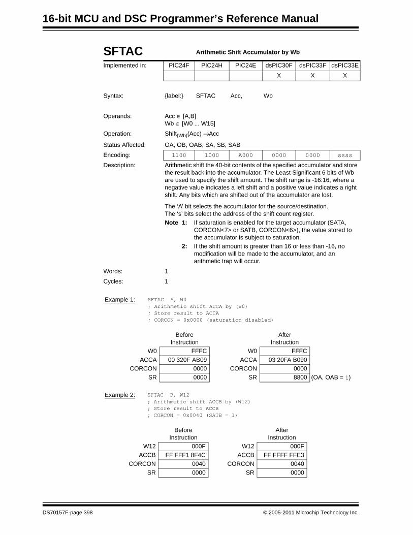
16-bit MCU and DSC Programmer’s Reference Manual
SFTAC Arithmetic Shift Accumulator by Wb
Implemented in: PIC24F PIC24H PIC24E dsPIC30F dsPIC33F dsPIC33E
X X X
Syntax: {label:} SFTAC Acc, Wb
Operands: Acc ∈ [A,B] Wb ∈ [W0 ... W15]
Operation: Shift(Wb)(Acc) → Acc
Status Affected: OA, OB, OAB, SA, SB, SAB
Encoding: 1100 1000 A000 0000 0000 ssss
Description: Arithmetic shift the 40-bit contents of the specified accumulator and store the result back into the accumulator. The Least Significant 6 bits of Wb are used to specify the shift amount. The shift range is -16:16, where a negative value indicates a left shift and a positive value indicates a right shift. Any bits which are shifted out of the accumulator are lost.
The ‘A’ bit selects the accumulator for the source/destination.The ‘s’ bits select the address of the shift count register.Note 1: If saturation is enabled for the target accumulator (SATA,
CORCON<7> or SATB, CORCON<6>), the value stored to the accumulator is subject to saturation.
2: If the shift amount is greater than 16 or less than -16, no modification will be made to the accumulator, and an arithmetic trap will occur.
Words: 1
Cycles: 1
Example 1: SFTAC A, W0 ; Arithmetic shift ACCA by (W0) ; Store result to ACCA ; CORCON = 0x0000 (saturation disabled)
Before Instruction
After Instruction
W0 FFFC W0 FFFCACCA 00 320F AB09 ACCA 03 20FA B090
CORCON 0000 CORCON 0000SR 0000 SR 8800 (OA, OAB = 1)
Example 2: SFTAC B, W12; Arithmetic shift ACCB by (W12); Store result to ACCB; CORCON = 0x0040 (SATB = 1)
Before Instruction
After Instruction
W12 000F W12 000FACCB FF FFF1 8F4C ACCB FF FFFF FFE3
CORCON 0040 CORCON 0040SR 0000 SR 0000
DS70157F-page 398 © 2005-2011 Microchip Technology Inc.
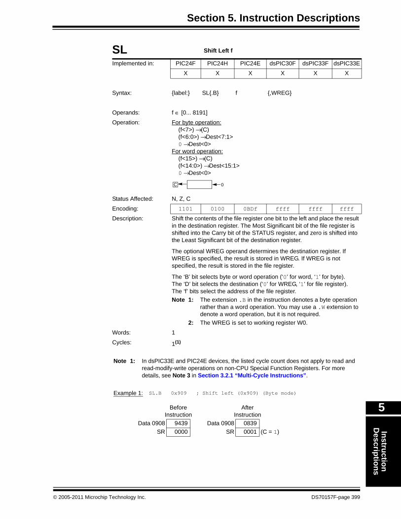
Section 5. Instruction DescriptionsInstruction
Descriptions
5
SL Shift Left f
Implemented in: PIC24F PIC24H PIC24E dsPIC30F dsPIC33F dsPIC33E
X X X X X X
Syntax: {label:} SL{.B} f {,WREG}
Operands: f ∈ [0... 8191]
Operation: For byte operation: (f<7>) → (C) (f<6:0>) → Dest<7:1> 0 → Dest<0>For word operation: (f<15>) → (C) (f<14:0>) → Dest<15:1> 0 → Dest<0>
Status Affected: N, Z, C
Encoding: 1101 0100 0BDf ffff ffff ffff
Description: Shift the contents of the file register one bit to the left and place the result in the destination register. The Most Significant bit of the file register is shifted into the Carry bit of the STATUS register, and zero is shifted into the Least Significant bit of the destination register.
The optional WREG operand determines the destination register. If WREG is specified, the result is stored in WREG. If WREG is not specified, the result is stored in the file register.
The ‘B’ bit selects byte or word operation (‘0’ for word, ‘1’ for byte).The ‘D’ bit selects the destination (‘0’ for WREG, ‘1’ for file register).The ‘f’ bits select the address of the file register.Note 1: The extension .B in the instruction denotes a byte operation
rather than a word operation. You may use a .W extension to denote a word operation, but it is not required.
2: The WREG is set to working register W0.
Words: 1
Cycles: 1(1)
Note 1: In dsPIC33E and PIC24E devices, the listed cycle count does not apply to read and read-modify-write operations on non-CPU Special Function Registers. For more details, see Note 3 in Section 3.2.1 “Multi-Cycle Instructions”.
C 0
Example 1: SL.B 0x909 ; Shift left (0x909) (Byte mode)
Before Instruction
After Instruction
Data 0908 9439 Data 0908 0839SR 0000 SR 0001 (C = 1)
© 2005-2011 Microchip Technology Inc. DS70157F-page 399

16-bit MCU and DSC Programmer’s Reference Manual
Example 2: SL 0x1650, WREG ; Shift left (0x1650) (Word mode) ; Store result in WREG
Before Instruction
After Instruction
WREG (W0) 0900 WREG (W0) 80CAData 1650 4065 Data 1650 4065
SR 0000 SR 0008 (N = 1)
DS70157F-page 400 © 2005-2011 Microchip Technology Inc.

Section 5. Instruction DescriptionsInstruction
Descriptions
5
SL Shift Left Ws
Implemented in: PIC24F PIC24H PIC24E dsPIC30F dsPIC33F dsPIC33E
X X X X X X
Syntax: {label:} SL{.B} Ws, Wd
[Ws], [Wd]
[Ws++], [Wd++]
[Ws--], [Wd--]
[++Ws], [++Wd]
[--Ws], [--Wd]
Operands: Ws ∈ [W0 ... W15]Wd ∈ [W0 ... W15]
Operation: For byte operation: (Ws<7>) → C (Ws<6:0>) → Wd<7:1> 0 → Wd<0>For word operation: (Ws<15>) → C (Ws<14:0>) → Wd<15:1> 0 → Wd<0>
Status Affected: N, Z, C
Encoding: 1101 0000 0Bqq qddd dppp ssss
Description: Shift the contents of the source register Ws one bit to the left and place the result in the destination register Wd. The Most Significant bit of Ws is shifted into the Carry bit of the STATUS register, and ‘0’ is shifted into the Least Significant bit of Wd. Either register direct or indirect addressing may be used for Ws and Wd.
The ‘B’ bit selects byte or word operation (‘0’ for word, ‘1’ for byte).The ‘q’ bits select the destination Address mode.The ‘d’ bits select the destination register.The ‘p’ bits select the source Address mode.The ‘s’ bits select the source register.
Note: The extension .B in the instruction denotes a byte operation rather than a word operation. You may use a .W extension to denote a word operation, but it is not required.
Words: 1
Cycles: 1(1)
Note 1: In dsPIC33E and PIC24E devices, the listed cycle count does not apply to read and read-modify-write operations on non-CPU Special Function Registers. For more details, see Note 3 in Section 3.2.1 “Multi-Cycle Instructions”.
C 0
© 2005-2011 Microchip Technology Inc. DS70157F-page 401

16-bit MCU and DSC Programmer’s Reference Manual
Example 1: SL.B W3, W4 ; Shift left W3 (Byte mode) ; Store result to W4
Before Instruction
After Instruction
W3 78A9 W3 78A9W4 1005 W4 1052SR 0000 SR 0001 (C = 1)
Example 2: SL [W2++], [W12] ; Shift left [W2] (Word mode) ; Store result to [W12] ; Post-increment W2
Before Instruction
After Instruction
W2 0900 W2 0902W12 1002 W12 1002
Data 0900 800F Data 0900 800FData 1002 6722 Data 1002 001E
SR 0000 SR 0001 (C = 1)
DS70157F-page 402 © 2005-2011 Microchip Technology Inc.
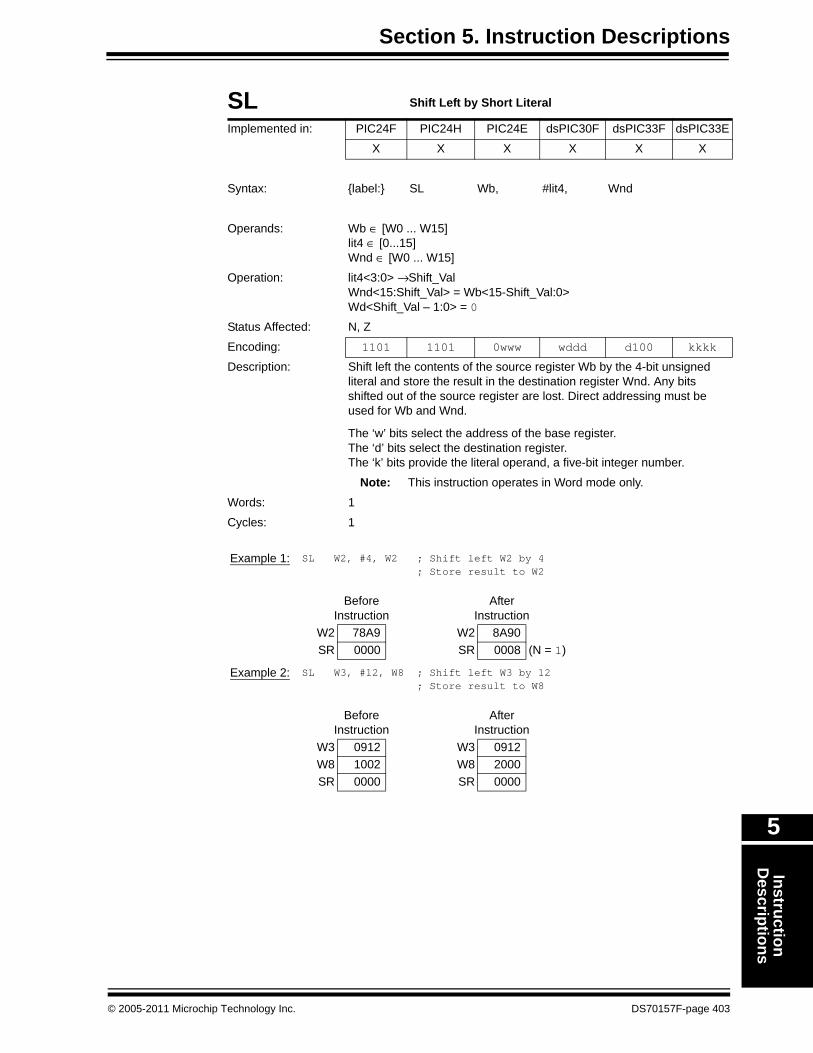
Section 5. Instruction DescriptionsInstruction
Descriptions
5
SL Shift Left by Short Literal
Implemented in: PIC24F PIC24H PIC24E dsPIC30F dsPIC33F dsPIC33E
X X X X X X
Syntax: {label:} SL Wb, #lit4, Wnd
Operands: Wb ∈ [W0 ... W15]lit4 ∈ [0...15]Wnd ∈ [W0 ... W15]
Operation: lit4<3:0> → Shift_ValWnd<15:Shift_Val> = Wb<15-Shift_Val:0>Wd<Shift_Val – 1:0> = 0
Status Affected: N, Z
Encoding: 1101 1101 0www wddd d100 kkkk
Description: Shift left the contents of the source register Wb by the 4-bit unsigned literal and store the result in the destination register Wnd. Any bits shifted out of the source register are lost. Direct addressing must be used for Wb and Wnd.
The ‘w’ bits select the address of the base register.The ‘d’ bits select the destination register.The ‘k’ bits provide the literal operand, a five-bit integer number.
Note: This instruction operates in Word mode only.
Words: 1
Cycles: 1
Example 1: SL W2, #4, W2 ; Shift left W2 by 4 ; Store result to W2
Before Instruction
After Instruction
W2 78A9 W2 8A90SR 0000 SR 0008 (N = 1)
Example 2: SL W3, #12, W8 ; Shift left W3 by 12 ; Store result to W8
Before Instruction
After Instruction
W3 0912 W3 0912W8 1002 W8 2000SR 0000 SR 0000
© 2005-2011 Microchip Technology Inc. DS70157F-page 403

16-bit MCU and DSC Programmer’s Reference Manual
SL Shift Left by Wns
Implemented in: PIC24F PIC24H PIC24E dsPIC30F dsPIC33F dsPIC33E
X X X X X X
Syntax: {label:} SL Wb, Wns, Wnd
Operands: Wb ∈ [W0 ... W15]Wns ∈ [W0 ...W15]Wnd ∈ [W0 ... W15]
Operation: Wns<4:0> → Shift_ValWnd<15:Shift_Val> = Wb<15 – Shift_Val:0>Wd<Shift_Val – 1:0> = 0
Status Affected: N, Z
Encoding: 1101 1101 0www wddd d000 ssss
Description: Shift left the contents of the source register Wb by the 5 Least Significant bits of Wns (only up to 15 positions) and store the result in the destination register Wnd. Any bits shifted out of the source register are lost. Register direct addressing must be used for Wb, Wns and Wnd.
The ‘w’ bits select the address of the base register.The ‘d’ bits select the destination register.The ‘s’ bits select the source register.Note 1: This instruction operates in Word mode only.
2: If Wns is greater than 15, Wnd will be loaded with 0x0.
Words: 1
Cycles: 1
Example 1: SL W0, W1, W2 ; Shift left W0 by W1<0:4> ; Store result to W2
Before Instruction
After Instruction
W0 09A4 W0 09A4W1 8903 W1 8903W2 78A9 W2 4D20SR 0000 SR 0000
Example 2: SL W4, W5, W6 ; Shift left W4 by W5<0:4> ; Store result to W6
Before Instruction
After Instruction
W4 A409 W4 A409W5 FF01 W5 FF01W6 0883 W6 4812SR 0000 SR 0000
DS70157F-page 404 © 2005-2011 Microchip Technology Inc.

Section 5. Instruction DescriptionsInstruction
Descriptions
5
SUB Subtract WREG from f
Implemented in: PIC24F PIC24H PIC24E dsPIC30F dsPIC33F dsPIC33E
X X X X X X
Syntax: {label:} SUB{.B} f {,WREG}
Operands: f ∈ [0 ... 8191]
Operation: (f) – (WREG) → destination designated by D
Status Affected: DC, N, OV, Z, C
Encoding: 1011 0101 0BDf ffff ffff ffff
Description: Subtract the contents of the default working register WREG from the contents of the specified file register, and place the result in the destination register. The optional WREG operand determines the destination register. If WREG is specified, the result is stored in WREG. If WREG is not specified, the result is stored in the file register.
The ‘B’ bit selects byte or word operation (‘0’ for word, ‘1’ for byte).The ‘D’ bit selects the destination (‘0’ for WREG, ‘1’ for file register).The ‘f’ bits select the address of the file register.Note 1: The extension .B in the instruction denotes a byte operation
rather than a word operation. You may use a .W extension to denote a word operation, but it is not required.
2: The WREG is set to working register W0.
Words: 1
Cycles: 1(1)
Note 1: In dsPIC33E and PIC24E devices, the listed cycle count does not apply to read and read-modify-write operations on non-CPU Special Function Registers. For more details, see Note 3 in Section 3.2.1 “Multi-Cycle Instructions”.
Example 1: SUB.B 0x1FFF ; Sub. WREG from (0x1FFF) (Byte mode) ; Store result to 0x1FFF
Before Instruction
After Instruction
WREG (W0) 7804 WREG (W0) 7804Data 1FFE 9439 Data 1FFE 9039
SR 0000 SR 0001 (C = 1)
Example 2: SUB 0xA04, WREG ; Sub. WREG from (0xA04) (Word mode) ; Store result to WREG
Before Instruction
After Instruction
WREG (W0) 6234 WREG (W0) E2EFData 0A04 4523 Data 0A04 4523
SR 0000 SR 0008 (N = 1)
© 2005-2011 Microchip Technology Inc. DS70157F-page 405
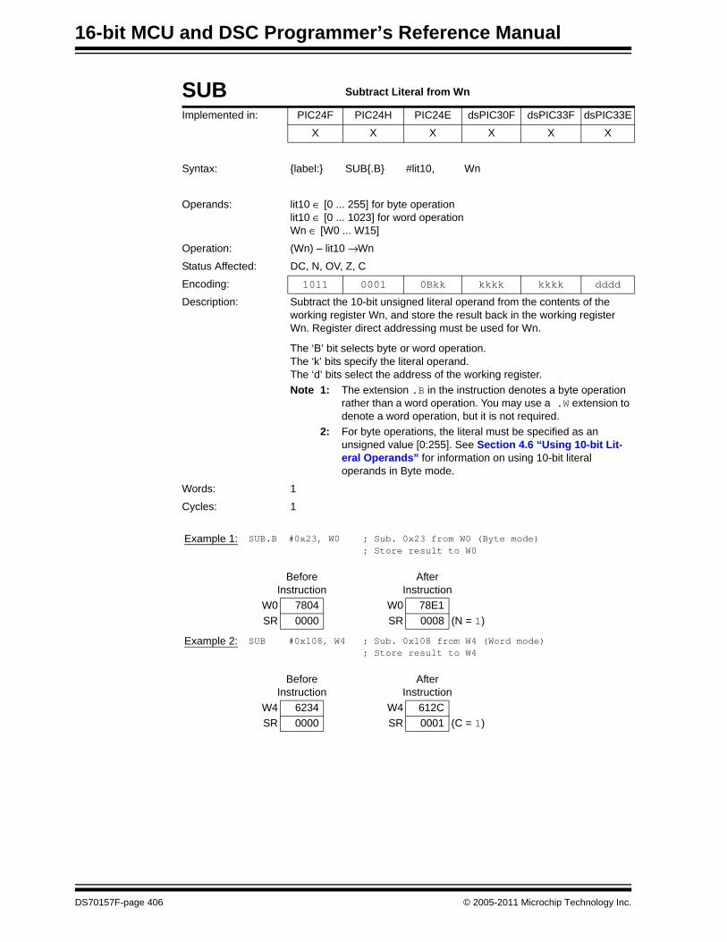
16-bit MCU and DSC Programmer’s Reference Manual
SUB Subtract Literal from Wn
Implemented in: PIC24F PIC24H PIC24E dsPIC30F dsPIC33F dsPIC33E
X X X X X X
Syntax: {label:} SUB{.B} #lit10, Wn
Operands: lit10 ∈ [0 ... 255] for byte operationlit10 ∈ [0 ... 1023] for word operationWn ∈ [W0 ... W15]
Operation: (Wn) – lit10 → Wn
Status Affected: DC, N, OV, Z, C
Encoding: 1011 0001 0Bkk kkkk kkkk dddd
Description: Subtract the 10-bit unsigned literal operand from the contents of the working register Wn, and store the result back in the working register Wn. Register direct addressing must be used for Wn.
The ‘B’ bit selects byte or word operation.The ‘k’ bits specify the literal operand.The ‘d’ bits select the address of the working register.Note 1: The extension .B in the instruction denotes a byte operation
rather than a word operation. You may use a .W extension to denote a word operation, but it is not required.
2: For byte operations, the literal must be specified as an unsigned value [0:255]. See Section 4.6 “Using 10-bit Lit-eral Operands” for information on using 10-bit literal operands in Byte mode.
Words: 1
Cycles: 1
Example 1: SUB.B #0x23, W0 ; Sub. 0x23 from W0 (Byte mode) ; Store result to W0
Before Instruction
After Instruction
W0 7804 W0 78E1SR 0000 SR 0008 (N = 1)
Example 2: SUB #0x108, W4 ; Sub. 0x108 from W4 (Word mode) ; Store result to W4
Before Instruction
After Instruction
W4 6234 W4 612CSR 0000 SR 0001 (C = 1)
DS70157F-page 406 © 2005-2011 Microchip Technology Inc.

Section 5. Instruction DescriptionsInstruction
Descriptions
5
SUB Subtract Short Literal from Wb
Implemented in: PIC24F PIC24H PIC24E dsPIC30F dsPIC33F dsPIC33EX X X X X X
Syntax: {label:} SUB{.B} Wb, #lit5, Wd[Wd][Wd++][Wd--][++Wd][--Wd]
Operands: Wb ∈ [W0 ... W15]lit5 ∈ [0 ... 31]Wd ∈ [W0 ... W15]
Operation: (Wb) – lit5 → Wd Status Affected: DC, N, OV, Z, CEncoding: 0101 0www wBqq qddd d11k kkkk
Description: Subtract the 5-bit unsigned literal operand from the contents of the base register Wb, and place the result in the destination register Wd. Register direct addressing must be used for Wb. Register direct or indirect addressing must be used for Wd.
The ‘w’ bits select the address of the base register.The ‘B’ bit selects byte or word operation (‘0’ for word, ‘1’ for byte).The ‘q’ bits select the destination Address mode.The ‘d’ bits select the destination register.The ‘k’ bits provide the literal operand, a five-bit integer number.
Note: The extension .B in the instruction denotes a byte operation rather than a word operation. You may use a .W extension to denote a word operation, but it is not required.
Words: 1Cycles: 1
Example 1: SUB.B W4, #0x10, W5 ; Sub. 0x10 from W4 (Byte mode) ; Store result to W5
Before Instruction
After Instruction
W4 1782 W4 1782W5 7804 W5 7872SR 0000 SR 0005 (OV, C = 1)
Example 2: SUB W0, #0x8, [W2++] ; Sub. 0x8 from W0 (Word mode) ; Store result to [W2] ; Post-increment W2
Before Instruction
After Instruction
W0 F230 W0 F230W2 2004 W2 2006
Data 2004 A557 Data 2004 F228SR 0000 SR 0009 (N, C = 1)
© 2005-2011 Microchip Technology Inc. DS70157F-page 407

16-bit MCU and DSC Programmer’s Reference Manual
SUB Subtract Ws from Wb
Implemented in: PIC24F PIC24H PIC24E dsPIC30F dsPIC33F dsPIC33E
X X X X X X
Syntax: {label:} SUB{.B} Wb, Ws, Wd
[Ws], [Wd]
[Ws++], [Wd++]
[Ws--], [Wd--]
[++Ws], [++Wd]
[--Ws], [--Wd]
Operands: Wb ∈ [W0 ... W15]Ws ∈ [W0 ... W15]Wd ∈ [W0 ... W15]
Operation: (Wb) – (Ws) → Wd
Status Affected: DC, N, OV, Z, C
Encoding: 0101 0www wBqq qddd dppp ssss
Description: Subtract the contents of the source register Ws from the contents of the base register Wb and place the result in the destination register Wd. Register direct addressing must be used for Wb. Either register direct or indirect addressing may be used for Ws and Wd.
The ‘w’ bits select the address of the base register.The ‘B’ bit selects byte or word operation (‘0’ for word, ‘1’ for byte).The ‘q’ bits select the destination Address mode.The ‘d’ bits select the destination register.The ‘p’ bits select the source Address mode.The ‘s’ bits select the source register.
Note: The extension .B in the instruction denotes a byte operation rather than a word operation. You may use a .W extension to denote a word operation, but it is not required.
Words: 1
Cycles: 1(1)
Note 1: In dsPIC33E and PIC24E devices, the listed cycle count does not apply to read and read-modify-write operations on non-CPU Special Function Registers. For more details, see Note 3 in Section 3.2.1 “Multi-Cycle Instructions”.
Example 1: SUB.B W0, W1, W0 ; Sub. W1 from W0 (Byte mode) ; Store result to W0
Before Instruction
After Instruction
W0 1732 W0 17EEW1 7844 W1 7844SR 0000 SR 0108 (DC, N = 1)
DS70157F-page 408 © 2005-2011 Microchip Technology Inc.

Section 5. Instruction DescriptionsInstruction
Descriptions
5
Example 2: SUB W7, [W8++], [W9++] ; Sub. [W8] from W7 (Word mode) ; Store result to [W9] ; Post-increment W8 ; Post-increment W9
Before Instruction
After Instruction
W7 2450 W7 2450W8 1808 W8 180AW9 2020 W9 2022
Data 1808 92E4 Data 1808 92E4Data 2020 A557 Data 2020 916C
SR 0000 SR 010C (DC, N, OV = 1)
© 2005-2011 Microchip Technology Inc. DS70157F-page 409

16-bit MCU and DSC Programmer’s Reference Manual
SUB Subtract Accumulators
Implemented in: PIC24F PIC24H PIC24E dsPIC30F dsPIC33F dsPIC33E
X X X
Syntax: {label:} SUB Acc
Operands: Acc ∈ [A,B]
Operation: If (Acc = A): ACCA – ACCB → ACCAElse: ACCB – ACCA → ACCB
Status Affected: OA, OB, OAB, SA, SB, SAB
Encoding: 1100 1011 A011 0000 0000 0000
Description: Subtract the contents of the unspecified accumulator from the contents of Acc, and store the result back into Acc. This instruction performs a 40-bit subtraction.
The ‘A’ bit specifies the destination accumulator.
Words: 1
Cycles: 1
Example 1: SUB A ; Subtract ACCB from ACCA ; Store the result to ACCA ; CORCON = 0x0000 (no saturation)
Before Instruction
After Instruction
ACCA 76 120F 098A ACCA 52 1EFC 4D73ACCB 23 F312 BC17 ACCB 23 F312 BC17
CORCON 0000 CORCON 0000SR 0000 SR 1100 (OA, OB = 1)
Example 2: SUB B ; Subtract ACCA from ACCB ; Store the result to ACCB ; CORCON = 0x0040 (SATB = 1)
Before Instruction
After Instruction
ACCA FF 9022 2EE1 ACCA FF 9022 2EE1ACCB 00 2456 8F4C ACCB 00 7FFF FFFF
CORCON 0040 CORCON 0040SR 0000 SR 1400 (SB, SAB = 1)
DS70157F-page 410 © 2005-2011 Microchip Technology Inc.

Section 5. Instruction DescriptionsInstruction
Descriptions
5
SUBB Subtract WREG and Carry bit from f
Implemented in: PIC24F PIC24H PIC24E dsPIC30F dsPIC33F dsPIC33E
X X X X X X
Syntax: {label:} SUBB{.B} f {,WREG}
Operands: f ∈ [0 ... 8191]
Operation: (f) – (WREG) – (C) → destination designated by D
Status Affected: DC, N, OV, Z, C
Encoding: 1011 0101 1BDf ffff ffff ffff
Description: Subtract the contents of the default working register WREG and the Borrow flag (Carry flag inverse, C) from the contents of the specified file register and place the result in the destination register. The optional WREG operand determines the destination register. If WREG is specified, the result is stored in WREG. If WREG is not specified, the result is stored in the file register
The ‘B’ bit selects byte or word operation (‘0’ for word, ‘1’ for byte).The ‘D’ bit selects the destination (‘0’ for WREG, ‘1’ for file register).The ‘f’ bits select the address of the file register.Note 1: The extension .B in the instruction denotes a byte operation
rather than a word operation. You may use a .W extension to denote a word operation, but it is not required.
2: The WREG is set to working register W0.3: The Z flag is “sticky” for ADDC, CPB, SUBB and SUBBR.
These instructions can only clear Z.
Words: 1
Cycles: 1(1)
Note 1: In dsPIC33E and PIC24E devices, the listed cycle count does not apply to read and read-modify-write operations on non-CPU Special Function Registers. For more details, see Note 3 in Section 3.2.1 “Multi-Cycle Instructions”.
Example 1: SUBB.B 0x1FFF ; Sub. WREG and C from (0x1FFF) (Byte mode) ; Store result to 0x1FFF
Before Instruction
After Instruction
WREG (W0) 7804 WREG (W0) 7804Data 1FFE 9439 Data 1FFE 8F39
SR 0000 SR 0011 (DC, C = 1)
Example 2: SUBB 0xA04, WREG ; Sub. WREG and C from (0xA04) (Word mode) ; Store result to WREG
Before Instruction
After Instruction
WREG (W0) 6234 WREG (W0) 0000Data 0A04 6235 Data 0A04 6235
SR 0000 SR 0001 (C = 1)
© 2005-2011 Microchip Technology Inc. DS70157F-page 411
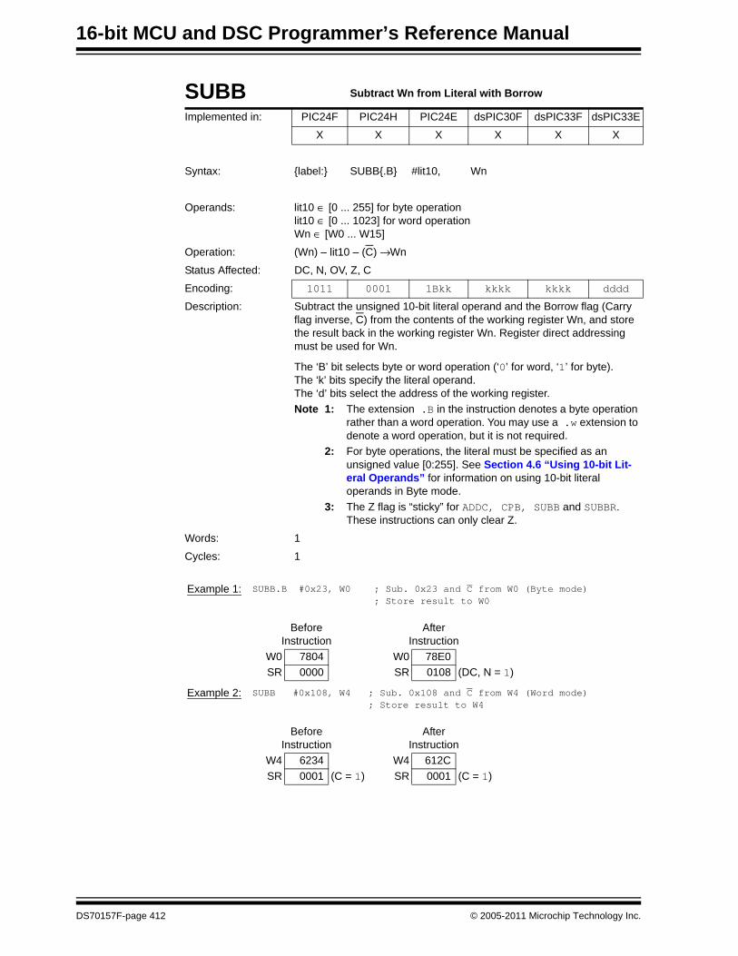
16-bit MCU and DSC Programmer’s Reference Manual
SUBB Subtract Wn from Literal with Borrow
Implemented in: PIC24F PIC24H PIC24E dsPIC30F dsPIC33F dsPIC33E
X X X X X X
Syntax: {label:} SUBB{.B} #lit10, Wn
Operands: lit10 ∈ [0 ... 255] for byte operationlit10 ∈ [0 ... 1023] for word operationWn ∈ [W0 ... W15]
Operation: (Wn) – lit10 – (C) → Wn
Status Affected: DC, N, OV, Z, C
Encoding: 1011 0001 1Bkk kkkk kkkk dddd
Description: Subtract the unsigned 10-bit literal operand and the Borrow flag (Carry flag inverse, C) from the contents of the working register Wn, and store the result back in the working register Wn. Register direct addressing must be used for Wn.
The ‘B’ bit selects byte or word operation (‘0’ for word, ‘1’ for byte).The ‘k’ bits specify the literal operand.The ‘d’ bits select the address of the working register.Note 1: The extension .B in the instruction denotes a byte operation
rather than a word operation. You may use a .w extension to denote a word operation, but it is not required.
2: For byte operations, the literal must be specified as an unsigned value [0:255]. See Section 4.6 “Using 10-bit Lit-eral Operands” for information on using 10-bit literal operands in Byte mode.
3: The Z flag is “sticky” for ADDC, CPB, SUBB and SUBBR. These instructions can only clear Z.
Words: 1
Cycles: 1
Example 1: SUBB.B #0x23, W0 ; Sub. 0x23 and C from W0 (Byte mode) ; Store result to W0
Before Instruction
After Instruction
W0 7804 W0 78E0SR 0000 SR 0108 (DC, N = 1)
Example 2: SUBB #0x108, W4 ; Sub. 0x108 and C from W4 (Word mode) ; Store result to W4
Before Instruction
After Instruction
W4 6234 W4 612CSR 0001 (C = 1) SR 0001 (C = 1)
DS70157F-page 412 © 2005-2011 Microchip Technology Inc.

Section 5. Instruction DescriptionsInstruction
Descriptions
5
SUBB Subtract Short Literal from Wb with Borrow
Implemented in: PIC24F PIC24H PIC24E dsPIC30F dsPIC33F dsPIC33E
X X X X X X
Syntax: {label:} SUBB{.B} Wb, #lit5, Wd
[Wd]
[Wd++]
[Wd--]
[++Wd]
[--Wd]
Operands: Wb ∈ [W0 ... W15]lit5 ∈ [0 ... 31]Wd ∈ [W0 ... W15]
Operation: (Wb) – lit5 – (C) → Wd
Status Affected: DC, N, OV, Z, C
Encoding: 0101 1www wBqq qddd d11k kkkk
Description: Subtract the 5-bit unsigned literal operand and the Borrow flag (Carry flag inverse, C) from the contents of the base register Wb and place the result in the destination register Wd. Register direct addressing must be used for Wb. Either register direct or indirect addressing may be used for Wd.
The ‘w’ bits select the address of the base register.The ‘B’ bit selects byte or word operation (‘0’ for word, ‘1’ for byte).The ‘q’ bits select the destination Address mode.The ‘d’ bits select the destination register.The ‘k’ bits provide the literal operand, a five-bit integer number.Note 1: The extension .B in the instruction denotes a byte operation
rather than a word operation. You may use a .W extension to denote a word operation, but it is not required.
2: The Z flag is “sticky” for ADDC, CPB, SUBB and SUBBR. These instructions can only clear Z.
Words: 1
Cycles: 1
Example 1: SUBB.B W4, #0x10, W5 ; Sub. 0x10 and C from W4 (Byte mode) ; Store result to W5
Before Instruction
After Instruction
W4 1782 W4 1782W5 7804 W5 7871SR 0000 SR 0005 (OV, C = 1)
© 2005-2011 Microchip Technology Inc. DS70157F-page 413

16-bit MCU and DSC Programmer’s Reference Manual
Example 2: SUBB W0, #0x8, [W2++] ; Sub. 0x8 and C from W0 (Word mode) ; Store result to [W2] ; Post-increment W2
Before Instruction
After Instruction
W0 0009 W0 0009W2 2004 W2 2006
Data 2004 A557 Data 2004 0000SR 0002 (Z = 1) SR 0103 (DC, Z, C = 1)
DS70157F-page 414 © 2005-2011 Microchip Technology Inc.

Section 5. Instruction DescriptionsInstruction
Descriptions
5
SUBB Subtract Ws from Wb with Borrow
Implemented in: PIC24F PIC24H PIC24E dsPIC30F dsPIC33F dsPIC33E
X X X X X X
Syntax: {label:} SUBB{.B} Wb, Ws, Wd
[Ws], [Wd]
[Ws++], [Wd++]
[Ws--], [Wd--]
[++Ws], [++Wd]
[--Ws], [--Wd]
Operands: Wb ∈ [W0 ... W15]Ws ∈ [W0 ... W15]Wd ∈ [W0 ... W15]
Operation: (Wb) – (Ws) – (C) → Wd
Status Affected: DC, N, OV, Z, C
Encoding: 0101 1www wBqq qddd dppp ssss
Description: Subtract the contents of the source register Ws and the Borrow flag (Carry flag inverse, C) from the contents of the base register Wb, and place the result in the destination register Wd. Register direct addressing must be used for Wb. Register direct or indirect addressing may be used for Ws and Wd.
The ‘w’ bits select the address of the base register.The ‘B’ bit selects byte or word operation (‘0’ for word, ‘1’ for byte).The ‘q’ bits select the destination Address mode.The ‘d’ bits select the destination register.The ‘p’ bits select the source Address mode.The ‘s’ bits select the source register.Note 1: The extension .B in the instruction denotes a byte operation
rather than a word operation. You may use a .W extension to denote a word operation, but it is not required.
2: The Z flag is “sticky” for ADDC, CPB, SUBB and SUBBR. These instructions can only clear Z.
Words: 1
Cycles: 1(1)
Note 1: In dsPIC33E and PIC24E devices, the listed cycle count does not apply to read and read-modify-write operations on non-CPU Special Function Registers. For more details, see Note 3 in Section 3.2.1 “Multi-Cycle Instructions”.
Example 1: SUBB.B W0, W1, W0 ; Sub. W1 and C from W0 (Byte mode) ; Store result to W0
Before Instruction
After Instruction
W0 1732 W0 17EDW1 7844 W1 7844SR 0000 SR 0108 (DC, N = 1)
© 2005-2011 Microchip Technology Inc. DS70157F-page 415
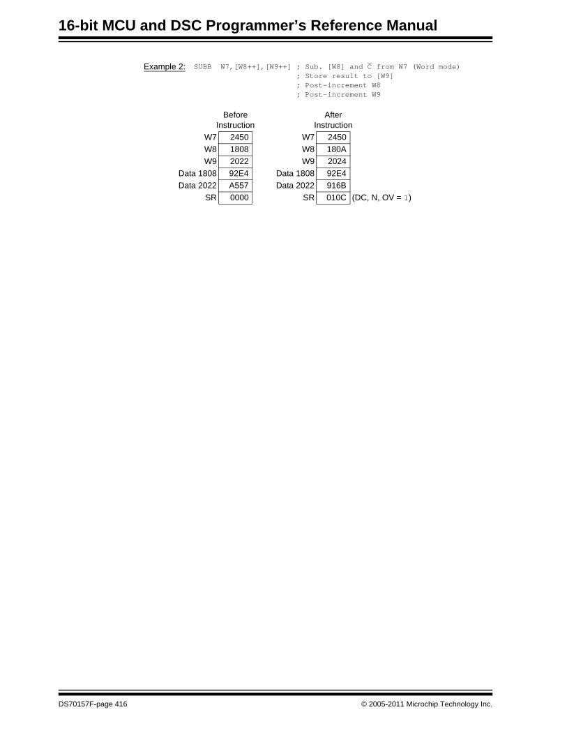
16-bit MCU and DSC Programmer’s Reference Manual
Example 2: SUBB W7,[W8++],[W9++] ; Sub. [W8] and C from W7 (Word mode) ; Store result to [W9] ; Post-increment W8 ; Post-increment W9
Before Instruction
After Instruction
W7 2450 W7 2450W8 1808 W8 180AW9 2022 W9 2024
Data 1808 92E4 Data 1808 92E4Data 2022 A557 Data 2022 916B
SR 0000 SR 010C (DC, N, OV = 1)
DS70157F-page 416 © 2005-2011 Microchip Technology Inc.

Section 5. Instruction DescriptionsInstruction
Descriptions
5
SUBBR Subtract f from WREG with Borrow
Implemented in: PIC24F PIC24H PIC24E dsPIC30F dsPIC33F dsPIC33E
X X X X X X
Syntax: {label:} SUBBR{.B} f {,WREG}
Operands: f ∈ [0 ... 8191]
Operation: (WREG) – (f) – (C) → destination designated by D
Status Affected: DC, N, OV, Z, C
Encoding: 1011 1101 1BDf ffff ffff ffff
Description: Subtract the contents of the specified file register f and the Borrow flag (Carry flag inverse, C) from the contents of WREG, and place the result in the destination register. The optional WREG operand determines the destination register. If WREG is specified, the result is stored in WREG. If WREG is not specified, the result is stored in the file register.
The ‘B’ bit selects byte or word operation (‘0’ for word, ‘1’ for byte).The ‘D’ bit selects the destination (‘0’ for WREG, ‘1’ for file register).The ‘f’ bits select the address of the file register.Note 1: The extension .B in the instruction denotes a byte operation
rather than a word operation. You may use a .W extension to denote a word operation, but it is not required.
2: The WREG is set to working register W0.3: The Z flag is “sticky” for ADDC, CPB, SUBB and SUBBR.
These instructions can only clear Z.
Words: 1
Cycles: 1(1)
Note 1: In dsPIC33E and PIC24E devices, the listed cycle count does not apply to read and read-modify-write operations on non-CPU Special Function Registers. For more details, see Note 3 in Section 3.2.1 “Multi-Cycle Instructions”.
Example 1: SUBBR.B 0x803 ; Sub. (0x803) and C from WREG (Byte mode) ; Store result to 0x803
Before Instruction
After Instruction
WREG (W0) 7804 WREG (W0) 7804Data 0802 9439 Data 0802 6F39
SR 0002 (Z = 1) SR 0000
Example 2: SUBBR 0xA04, WREG ; Sub. (0xA04) and C from WREG (Word mode) ; Store result to WREG
Before Instruction
After Instruction
WREG (W0) 6234 WREG (W0) FFFEData 0A04 6235 Data 0A04 6235
SR 0000 SR 0008 (N = 1)
© 2005-2011 Microchip Technology Inc. DS70157F-page 417

16-bit MCU and DSC Programmer’s Reference Manual
SUBBR Subtract Wb from Short Literal with Borrow
Implemented in: PIC24F PIC24H PIC24E dsPIC30F dsPIC33F dsPIC33E
X X X X X X
Syntax: {label:} SUBBR{.B} Wb, #lit5, Wd
[Wd]
[Wd++]
[Wd--]
[++Wd]
[--Wd]
Operands: Wb ∈ [W0 ... W15]lit5 ∈ [0 ... 31]Wd ∈ [W0 ... W15]
Operation: lit5 – (Wb) – (C) → Wd
Status Affected: DC, N, OV, Z, C
Encoding: 0001 1www wBqq qddd d11k kkkk
Description: Subtract the contents of the base register Wb and the Borrow flag (Carry flag inverse, C) from the 5-bit unsigned literal and place the result in the destination register Wd. Register direct addressing must be used for Wb. Register direct or indirect addressing must be used for Wd.
The ‘w’ bits select the address of the base register.The ‘B’ bit selects byte or word operation (‘0’ for word, ‘1’ for byte).The ‘q’ bits select the destination Address mode.The ‘d’ bits select the destination register.The ‘k’ bits provide the literal operand, a five-bit integer number.Note 1: The extension .B in the instruction denotes a byte operation
rather than a word operation. You may use a .W extension to denote a word operation, but it is not required.
2: The Z flag is “sticky” for ADDC, CPB, SUBB and SUBBR. These instructions can only clear Z.
Words: 1
Cycles: 1
Example 1: SUBBR.B W0, #0x10, W1 ; Sub. W0 and C from 0x10 (Byte mode) ; Store result to W1
Before Instruction
After Instruction
W0 F310 W0 F310W1 786A W1 7800SR 0003 (Z, C = 1) SR 0103 (DC, Z, C = 1)
DS70157F-page 418 © 2005-2011 Microchip Technology Inc.

Section 5. Instruction DescriptionsInstruction
Descriptions
5
Example 2: SUBBR W0, #0x8, [W2++] ; Sub. W0 and C from 0x8 (Word mode) ; Store result to [W2] ; Post-increment W2
Before Instruction
After Instruction
W0 0009 W0 0009W2 2004 W2 2006
Data 2004 A557 Data 2004 FFFESR 0020 (Z = 1) SR 0108 (DC, N = 1)
© 2005-2011 Microchip Technology Inc. DS70157F-page 419

16-bit MCU and DSC Programmer’s Reference Manual
SUBBR Subtract Wb from Ws with Borrow
Implemented in: PIC24F PIC24H PIC24E dsPIC30F dsPIC33F dsPIC33E
X X X X X X
Syntax: {label:} SUBBR{.B} Wb, Ws, Wd
[Ws], [Wd]
[Ws++], [Wd++]
[Ws--], [Wd--]
[++Ws], [++Wd]
[--Ws], [--Wd]
Operands: Wb ∈ [W0 ... W15]Ws ∈ [W0 ... W15]Wd ∈ [W0 ... W15]
Operation: (Ws) – (Wb) – (C) → Wd
Status Affected: DC, N, OV, Z, C
Encoding: 0001 1www wBqq qddd dppp ssss
Description: Subtract the contents of the base register Wb and the Borrow flag (Carry flag inverse, C) from the contents of the source register Ws and place the result in the destination register Wd. Register direct addressing must be used for Wb. Register direct or indirect addressing may be used for Ws and Wd.
The ‘w’ bits select the address of the base register.The ‘B’ bit selects byte or word operation (‘0’ for word, ‘1’ for byte).The ‘q’ bits select the destination Address mode.The ‘d’ bits select the destination register.The ‘p’ bits select the source Address mode.The ‘s’ bits select the source register.Note 1: The extension .B in the instruction denotes a byte operation
rather than a word operation. You may use a .W extension to denote a word operation, but it is not required.
2: The Z flag is “sticky” for ADDC, CPB, SUBB and SUBBR. These instructions can only clear Z.
Words: 1
Cycles: 1(1)
Note 1: In dsPIC33E and PIC24E devices, the listed cycle count does not apply to read and read-modify-write operations on non-CPU Special Function Registers. For more details, see Note 3 in Section 3.2.1 “Multi-Cycle Instructions”.
Example 1: SUBBR.B W0, W1, W0 ; Sub. W0 and C from W1 (Byte mode) ; Store result to W0
Before Instruction
After Instruction
W0 1732 W0 1711W1 7844 W1 7844SR 0000 SR 0001 (C = 1)
DS70157F-page 420 © 2005-2011 Microchip Technology Inc.

Section 5. Instruction DescriptionsInstruction
Descriptions
5
Example 2: SUBBR W7,[W8++],[W9++] ; Sub. W7 and C from [W8] (Word mode) ; Store result to [W9] ; Post-increment W8 ; Post-increment W9
Before Instruction
After Instruction
W7 2450 W7 2450W8 1808 W8 180AW9 2022 W9 2024
Data 1808 92E4 Data 1808 92E4Data 2022 A557 Data 2022 6E93
SR 0000 SR 0005 (OV, C = 1)
© 2005-2011 Microchip Technology Inc. DS70157F-page 421

16-bit MCU and DSC Programmer’s Reference Manual
SUBR Subtract f from WREG
Implemented in: PIC24F PIC24H PIC24E dsPIC30F dsPIC33F dsPIC33E
X X X X X X
Syntax: {label:} SUBR{.B} f {,WREG}
Operands: f ∈ [0 ... 8191]
Operation: (WREG) – (f) → destination designated by D
Status Affected: DC, N, OV, Z, C
Encoding: 1011 1101 0BDf ffff ffff ffff
Description: Subtract the contents of the specified file register from the contents of the default working register WREG, and place the result in the destination register. The optional WREG operand determines the destination register. If WREG is specified, the result is stored in WREG. If WREG is not specified, the result is stored in the file register
The ‘B’ bit selects byte or word operation (‘0’ for word, ‘1’ for byte).The ‘D’ bit selects the destination (‘0’ for WREG, ‘1’ for file register).The ‘f’ bits select the address of the file register.Note 1: The extension .B in the instruction denotes a byte operation
rather than a word operation. You may use a .W extension to denote a word operation, but it is not required.
2: The WREG is set to working register W0.
Words: 1
Cycles: 1(1)
Note 1: In dsPIC33E and PIC24E devices, the listed cycle count does not apply to read and read-modify-write operations on non-CPU Special Function Registers. For more details, see Note 3 in Section 3.2.1 “Multi-Cycle Instructions”.
Example 1: SUBR.B 0x1FFF ; Sub. (0x1FFF) from WREG (Byte mode) ; Store result to 0x1FFF
Before Instruction
After Instruction
WREG (W0) 7804 WREG (W0) 7804Data 1FFE 9439 Data 1FFE 7039
SR 0000 SR 0000
Example 2: SUBR 0xA04, WREG ; Sub. (0xA04) from WREG (Word mode) ; Store result to WREG
Before Instruction
After Instruction
WREG (W0) 6234 WREG (W0) FFFFData 0A04 6235 Data 0A04 6235
SR 0000 SR 0008 (N = 1)
DS70157F-page 422 © 2005-2011 Microchip Technology Inc.

Section 5. Instruction DescriptionsInstruction
Descriptions
5
SUBR Subtract Wb from Short Literal
Implemented in: PIC24F PIC24H PIC24E dsPIC30F dsPIC33F dsPIC33EX X X X X X
Syntax: {label:} SUBR{.B} Wb, #lit5 Wd[Wd][Wd++][Wd--][++Wd][--Wd]
Operands: Wb ∈ [W0 ... W15]lit5 ∈ [0 ... 31]Wd ∈ [W0 ... W15]
Operation: lit5 – (Wb) → Wd Status Affected: DC, N, OV, Z, CEncoding: 0001 0www wBqq qddd d11k kkkk
Description: Subtract the contents of the base register Wb from the unsigned 5-bit literal operand, and place the result in the destination register Wd. Register direct addressing must be used for Wb. Either register direct or indirect addressing may be used for Wd.
The ‘w’ bits select the address of the base register.The ‘B’ bit selects byte or word operation (‘0’ for word, ‘1’ for byte).The ‘q’ bits select the destination Address mode.The ‘d’ bits select the destination register.The ‘k’ bits provide the literal operand, a five-bit integer number.
Note: The extension .B in the instruction denotes a byte operation rather than a word operation. You may use a .W extension to denote a word operation, but it is not required.
Words: 1Cycles: 1
Example 1: SUBR.B W0, #0x10, W1 ; Sub. W0 from 0x10 (Byte mode) ; Store result to W1
Before Instruction
After Instruction
W0 F310 W0 F310W1 786A W1 7800SR 0000 SR 0103 (DC, Z, C = 1)
Example 2: SUBR W0, #0x8, [W2++] ; Sub. W0 from 0x8 (Word mode) ; Store result to [W2] ; Post-increment W2
Before Instruction
After Instruction
W0 0009 W0 0009W2 2004 W2 2006
Data 2004 A557 Data 2004 FFFFSR 0000 SR 0108 (DC, N = 1)
© 2005-2011 Microchip Technology Inc. DS70157F-page 423

16-bit MCU and DSC Programmer’s Reference Manual
SUBR Subtract Wb from Ws
Implemented in: PIC24F PIC24H PIC24E dsPIC30F dsPIC33F dsPIC33E
X X X X X X
Syntax: {label:} SUBR{.B} Wb, Ws, Wd
[Ws], [Wd]
[Ws++], [Wd++]
[Ws--], [Wd--]
[++Ws], [++Wd]
[--Ws], [--Wd]
Operands: Wb ∈ [W0 ... W15]Ws ∈ [W0 ... W15]Wd ∈ [W0 ... W15]
Operation: (Ws) – (Wb) → Wd
Status Affected: DC, N, OV, Z, C
Encoding: 0001 0www wBqq qddd dppp ssss
Description: Subtract the contents of the base register Wb from the contents of the source register Ws and place the result in the destination register Wd. Register direct addressing must be used for Wb. Either register direct or indirect addressing may be used for Ws and Wd.
The ‘w’ bits select the address of the base register.The ‘B’ bit selects byte or word operation (‘0’ for word, ‘1’ for byte).The ‘q’ bits select the destination Address mode.The ‘d’ bits select the destination register.The ‘p’ bits select the source Address mode.The ‘s’ bits select the source register.
Note: The extension .B in the instruction denotes a byte operation rather than a word operation. You may use a .W extension to denote a word operation, but it is not required.
Words: 1
Cycles: 1(1)
Note 1: In dsPIC33E and PIC24E devices, the listed cycle count does not apply to read and read-modify-write operations on non-CPU Special Function Registers. For more details, see Note 3 in Section 3.2.1 “Multi-Cycle Instructions”.
Example 1: SUBR.B W0, W1, W0 ; Sub. W0 from W1 (Byte mode) ; Store result to W0
Before Instruction
After Instruction
W0 1732 W0 1712W1 7844 W1 7844SR 0000 SR 0001 (C = 1)
DS70157F-page 424 © 2005-2011 Microchip Technology Inc.

Section 5. Instruction DescriptionsInstruction
Descriptions
5
Example 2: SUBR W7, [W8++], [W9++] ; Sub. W7 from [W8] (Word mode) ; Store result to [W9] ; Post-increment W8 ; Post-increment W9
Before Instruction
After Instruction
W7 2450 W7 2450W8 1808 W8 180AW9 2022 W9 2024
Data 1808 92E4 Data 1808 92E4Data 2022 A557 Data 2022 6E94
SR 0000 SR 0005 (OV, C = 1)
© 2005-2011 Microchip Technology Inc. DS70157F-page 425

16-bit MCU and DSC Programmer’s Reference Manual
SWAP Byte or Nibble Swap Wn
Implemented in: PIC24F PIC24H PIC24E dsPIC30F dsPIC33F dsPIC33E
X X X X X X
Syntax: {label:} SWAP{.B} Wn
Operands: Wn ∈ [W0 ... W15]
Operation: For byte operation: (Wn)<7:4> ↔ (Wn)<3:0> For word operation: (Wn)<15:8> ↔ (Wn)<7:0>
Status Affected: None
Encoding: 1111 1101 1B00 0000 0000 ssss
Description: Swap the contents of the working register Wn. In Word mode, the two bytes of Wn are swapped. In Byte mode, the two nibbles of the Least Significant Byte of Wn are swapped, and the Most Significant Byte of Wn is unchanged. Register direct addressing must be used for Wn.
The ‘B’ bit selects byte or word operation (‘0’ for word, ‘1’ for byte).The ‘s’ bits select the address of the working register.
Note: The extension .B in the instruction denotes a byte operation rather than a word operation. You may use a .W extension to denote a word operation, but it is not required.
Words: 1
Cycles: 1
Example 1: SWAP.B W0 ; Nibble swap (W0)
Before Instruction
After Instruction
W0 AB87 W0 AB78SR 0000 SR 0000
Example 2: SWAP W0 ; Byte swap (W0)
Before Instruction
After Instruction
W0 8095 W0 9580SR 0000 SR 0000
DS70157F-page 426 © 2005-2011 Microchip Technology Inc.

Section 5. Instruction DescriptionsInstruction
Descriptions
5
TBLRDH Table Read High
Implemented in: PIC24F PIC24H PIC24E dsPIC30F dsPIC33F dsPIC33E
X X X X X X
Syntax: {label:} TBLRDH{.B} [Ws], Wd
[Ws++], [Wd]
[Ws--], [Wd++]
[++Ws], [Wd--]
[--Ws], [++Wd]
[--Wd]
Operands: Ws ∈ [W0 ... W15]Wd ∈ [W0 ... W15]
Operation: For byte operation: If (LSB(Ws) = 1) 0 → Wd Else Program Mem [(TBLPAG),(Ws)] <23:16> → WdFor word operation: Program Mem [(TBLPAG),(Ws)] <23:16> → Wd <7:0> 0 → Wd <15:8>
Status Affected: None
Encoding: 1011 1010 1Bqq qddd dppp ssss
Description: Read the contents of the most significant word of program memory and store it to the destination register Wd. The target word address of program memory is formed by concatenating the 8-bit Table Pointer register, TBLPAG<7:0>, with the effective address specified by Ws. Indirect addressing must be used for Ws, and either register direct or indirect addressing may be used for Wd.
In Word mode, zero is stored to the Most Significant Byte of the destination register (due to non-existent program memory) and the third program memory byte (PM<23:16>) at the specified program memory address is stored to the Least Significant Byte of the destination register.
In Byte mode, the source address depends on the contents of Ws. If Ws is not word-aligned, zero is stored to the destination register (due to non-existent program memory). If Ws is word-aligned, the third program memory byte (PM<23:16>) at the specified program memory address is stored to the destination register.
The ‘B’ bit selects byte or word operation (‘0’ for word, ‘1’ for byte).The ‘q’ bits select the destination Address mode.The ‘d’ bits select the destination register.The ‘p’ bits select the source Address mode.The ‘s’ bits select the source register.
Note: The extension .B in the instruction denotes a byte move rather than a word move. You may use a .W extension to denote a word move, but it is not required.
Words: 1
Cycles: 2 (PIC24F, PIC24H, dsPIC30F, dsPIC33F)
5 (PIC24E, dsPIC33E)
© 2005-2011 Microchip Technology Inc. DS70157F-page 427

16-bit MCU and DSC Programmer’s Reference Manual
Example 1: TBLRDH.B [W0], [W1++] ; Read PM (TBLPAG:[W0]) (Byte mode) ; Store to [W1] ; Post-increment W1
Before Instruction
After Instruction
W0 0812 W0 0812W1 0F71 W1 0F72
Data 0F70 0944 Data 0F70 EF44Program 01 0812 EF 2042 Program 01 0812 EF 2042
TBLPAG 0001 TBLPAG 0001SR 0000 SR 0000
Example 2: TBLRDH [W6++], W8 ; Read PM (TBLPAG:[W6]) (Word mode) ; Store to W8 ; Post-increment W6
Before Instruction
After Instruction
W6 3406 W6 3408W8 65B1 W8 0029
Program 00 3406 29 2E40 Program 00 3406 29 2E40 TBLPAG 0000 TBLPAG 0000
SR 0000 SR 0000
DS70157F-page 428 © 2005-2011 Microchip Technology Inc.

Section 5. Instruction DescriptionsInstruction
Descriptions
5
TBLRDL Table Read Low
Implemented in: PIC24F PIC24H PIC24E dsPIC30F dsPIC33F dsPIC33E
X X X X X X
Syntax: {label:} TBLRDL{.B} [Ws], Wd
[Ws++], [Wd]
[Ws--], [Wd++]
[++Ws], [Wd--]
[--Ws], [++Wd]
[--Wd]
Operands: Ws ∈ [W0 ... W15]Wd ∈ [W0 ... W15]
Operation: For byte operation: If (LSB(Ws) = 1) Program Mem [(TBLPAG),(Ws)] <15:8> → Wd Else Program Mem [(TBLPAG),(Ws)] <7:0> → WdFor word operation: Program Mem [(TBLPAG),(Ws)] <15:0> → Wd
Status Affected: None
Encoding: 1011 1010 0Bqq qddd dppp ssss
Description: Read the contents of the least significant word of program memory and store it to the destination register Wd. The target word address of program memory is formed by concatenating the 8-bit Table Pointer register, TBLPAG<7:0>, with the effective address specified by Ws. Indirect addressing must be used for Ws, and either register direct or indirect addressing may be used for Wd.
In Word mode, the lower 2 bytes of program memory are stored to the destination register. In Byte mode, the source address depends on the contents of Ws. If Ws is not word-aligned, the second byte of the program memory word (PM<15:7>) is stored to the destination register. If Ws is word-aligned, the first byte of the program memory word (PM<7:0>) is stored to the destination register.
The ‘B’ bit selects byte or word operation (‘0’ for word mode, ‘1’ for byte).The ‘q’ bits select the destination Address mode.The ‘d’ bits select the destination register.The ‘p’ bits select the source Address mode.The ‘s’ bits select the source register.
Note: The extension .B in the instruction denotes a byte move rather than a word move. You may use a .W extension to denote a word move, but it is not required.
Words: 1
Cycles: 2 (PIC24F, PIC24H, dsPIC30F, dsPIC33F)
5 (PIC24E, dsPIC33E)
© 2005-2011 Microchip Technology Inc. DS70157F-page 429

16-bit MCU and DSC Programmer’s Reference Manual
Example 1: TBLRDL.B [W0++], W1 ; Read PM (TBLPAG:[W0]) (Byte mode) ; Store to W1 ; Post-increment W0
Before Instruction
After Instruction
W0 0813 W0 0814W1 0F71 W1 0F20
Data 0F70 0944 Data 0F70 EF44Program 01 0812 EF 2042 Program 01 0812 EF 2042
TBLPAG 0001 TBLPAG 0001SR 0000 SR 0000
Example 2: TBLRDL [W6], [W8++] ; Read PM (TBLPAG:[W6]) (Word mode) ; Store to W8 ; Post-increment W8
Before Instruction
After Instruction
W6 3406 W6 3406W8 1202 W8 1204
Data 1202 658B Data 1202 2E40Program 00 3406 29 2E40 Program 00 3406 29 2E40
TBLPAG 0000 TBLPAG 0000SR 0000 SR 0000
DS70157F-page 430 © 2005-2011 Microchip Technology Inc.

Section 5. Instruction DescriptionsInstruction
Descriptions
5
TBLWTH Table Write High
Implemented in: PIC24F PIC24H PIC24E dsPIC30F dsPIC33F dsPIC33E
X X X X X X
Syntax: {label:} TBLWTH{.B} Ws, [Wd]
[Ws], [Wd++]
[Ws++], [Wd--]
[Ws--], [++Wd]
[++Ws], [--Wd]
[--Ws],
Operands: Ws ∈ [W0 ... W15]Wd ∈ [W0 ... W15]
Operation: For byte operation: If (LSB(Wd) = 1) NOP Else (Ws) → Program Mem [(TBLPAG),(Wd)]<23:16>For word operation: (Ws)<7:0> → Program Mem [(TBLPAG),(Wd)] <23:16>
Status Affected: None
Encoding: 1011 1011 1Bqq qddd dppp ssss
Description: Store the contents of the working source register Ws to the most significant word of program memory. The destination word address of program memory is formed by concatenating the 8-bit Table Pointer register, TBLPAG<7:0>, with the effective address specified by Wd. Either direct or indirect addressing may be used for Ws, and indirect addressing must be used for Wd.
Since program memory is 24 bits wide, this instruction can only write to the upper byte of program memory (PM<23:16>). This may be performed using a Wd that is word-aligned in Byte mode or Word mode. If Byte mode is used with a Wd that is not word-aligned, no operation is performed.
The ‘B’ bit selects byte or word operation (‘0’ for word, ‘1’ for byte).The ‘q’ bits select the destination Address mode.The ‘d’ bits select the destination register.The ‘p’ bits select the source Address mode.The ‘s’ bits select the source register.
Note: The extension .B in the instruction denotes a byte move rather than a word move. You may use a .W extension to denote a word move, but it is not required.
Words: 1
Cycles: 2(1)
Note 1: In dsPIC33E and PIC24E devices, the listed cycle count does not apply to read and read-modify-write operations on non-CPU Special Function Registers. For more details, see Note 3 in Section 3.2.1 “Multi-Cycle Instructions”.
© 2005-2011 Microchip Technology Inc. DS70157F-page 431

16-bit MCU and DSC Programmer’s Reference Manual
Example 1: TBLWTH.B [W0++], [W1] ; Write [W0]... (Byte mode) ; to PM Latch High (TBLPAG:[W1]) ; Post-increment W0
Before Instruction
After Instruction
W0 0812 W0 0814W1 0F70 W1 0F70
Data 0812 0944 Data 0812 EF44Program 01 0F70 EF 2042 Program 01 0F70 44 2042
TBLPAG 0001 TBLPAG 0001SR 0000 SR 0000
Note: Only the Program Latch is written to. The contents of program memory are not updated until the Flash memory is programmed using the procedure described in the specific device family reference manual.
Example 2: TBLWTH W6, [W8++] ; Write W6... (Word mode) ; to PM Latch High (TBLPAG:[W8]) ; Post-increment W8
Before Instruction
After Instruction
W6 0026 W6 0026W8 0870 W8 0872
Program 00 0870 22 3551 Program 00 0870 26 3551 TBLPAG 0000 TBLPAG 0000
SR 0000 SR 0000
Note: Only the Program Latch is written to. The contents of program memory are not updated until the Flash memory is programmed using the procedure described in the specific device family reference manual.
DS70157F-page 432 © 2005-2011 Microchip Technology Inc.
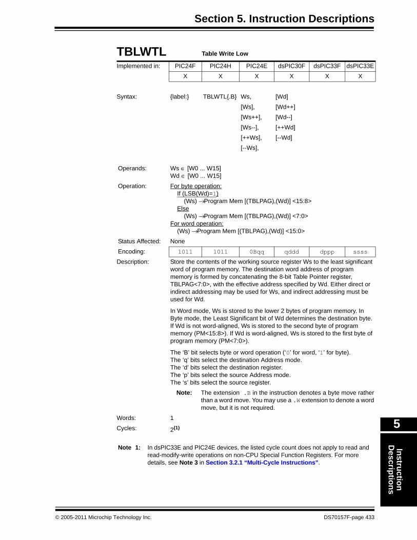
Section 5. Instruction DescriptionsInstruction
Descriptions
5
TBLWTL Table Write Low
Implemented in: PIC24F PIC24H PIC24E dsPIC30F dsPIC33F dsPIC33E
X X X X X X
Syntax: {label:} TBLWTL{.B} Ws, [Wd]
[Ws], [Wd++]
[Ws++], [Wd--]
[Ws--], [++Wd]
[++Ws], [--Wd]
[--Ws],
Operands: Ws ∈ [W0 ... W15]Wd ∈ [W0 ... W15]
Operation: For byte operation: If (LSB(Wd)=1) (Ws) → Program Mem [(TBLPAG),(Wd)] <15:8> Else (Ws) → Program Mem [(TBLPAG),(Wd)] <7:0>For word operation: (Ws) → Program Mem [(TBLPAG),(Wd)] <15:0>
Status Affected: None
Encoding: 1011 1011 0Bqq qddd dppp ssss
Description: Store the contents of the working source register Ws to the least significant word of program memory. The destination word address of program memory is formed by concatenating the 8-bit Table Pointer register, TBLPAG<7:0>, with the effective address specified by Wd. Either direct or indirect addressing may be used for Ws, and indirect addressing must be used for Wd.
In Word mode, Ws is stored to the lower 2 bytes of program memory. In Byte mode, the Least Significant bit of Wd determines the destination byte. If Wd is not word-aligned, Ws is stored to the second byte of program memory (PM<15:8>). If Wd is word-aligned, Ws is stored to the first byte of program memory (PM<7:0>).
The ‘B’ bit selects byte or word operation (‘0’ for word, ‘1’ for byte).The ‘q’ bits select the destination Address mode.The ‘d’ bits select the destination register.The ‘p’ bits select the source Address mode.The ‘s’ bits select the source register.
Note: The extension .B in the instruction denotes a byte move rather than a word move. You may use a .W extension to denote a word move, but it is not required.
Words: 1
Cycles: 2(1)
Note 1: In dsPIC33E and PIC24E devices, the listed cycle count does not apply to read and read-modify-write operations on non-CPU Special Function Registers. For more details, see Note 3 in Section 3.2.1 “Multi-Cycle Instructions”.
© 2005-2011 Microchip Technology Inc. DS70157F-page 433
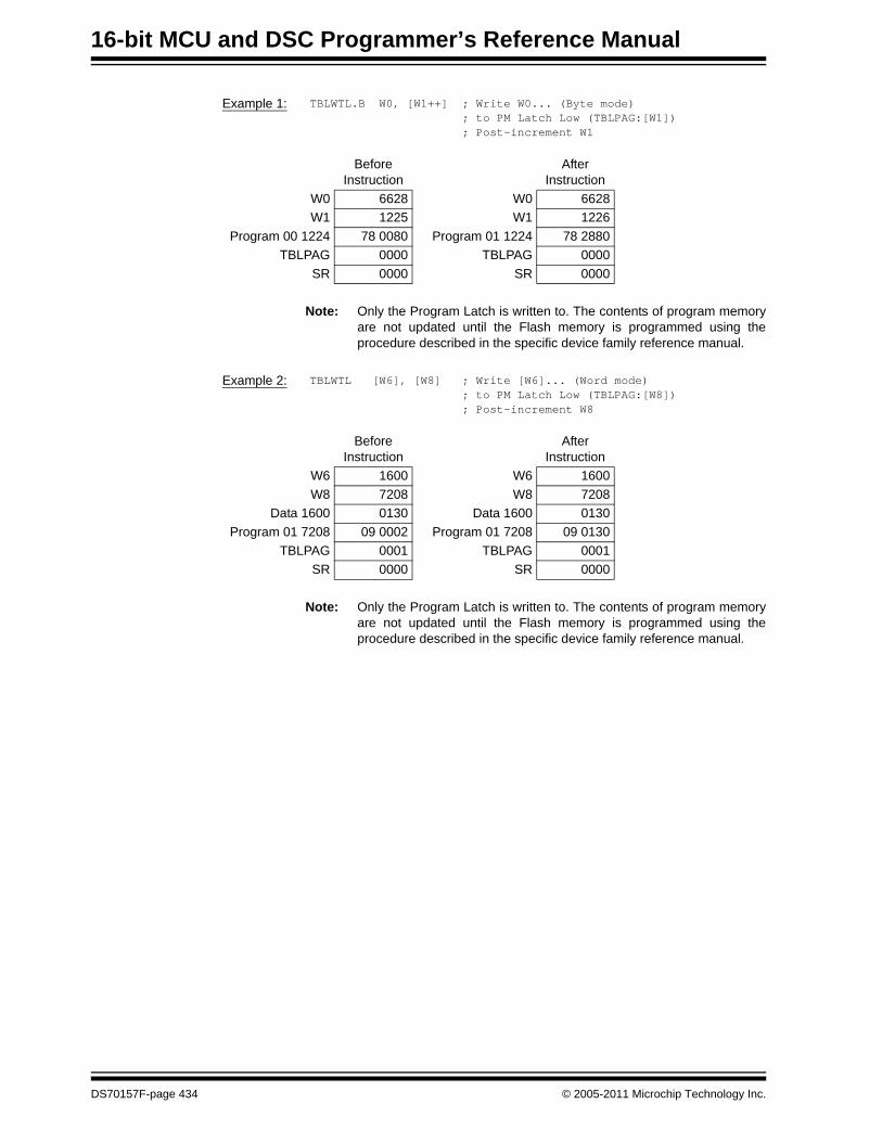
16-bit MCU and DSC Programmer’s Reference Manual
Example 1: TBLWTL.B W0, [W1++] ; Write W0... (Byte mode) ; to PM Latch Low (TBLPAG:[W1]) ; Post-increment W1
Before Instruction
After Instruction
W0 6628 W0 6628W1 1225 W1 1226
Program 00 1224 78 0080 Program 01 1224 78 2880 TBLPAG 0000 TBLPAG 0000
SR 0000 SR 0000
Note: Only the Program Latch is written to. The contents of program memory are not updated until the Flash memory is programmed using the procedure described in the specific device family reference manual.
Example 2: TBLWTL [W6], [W8] ; Write [W6]... (Word mode) ; to PM Latch Low (TBLPAG:[W8]) ; Post-increment W8
Before Instruction
After Instruction
W6 1600 W6 1600W8 7208 W8 7208
Data 1600 0130 Data 1600 0130Program 01 7208 09 0002 Program 01 7208 09 0130
TBLPAG 0001 TBLPAG 0001SR 0000 SR 0000
Note: Only the Program Latch is written to. The contents of program memory are not updated until the Flash memory is programmed using the procedure described in the specific device family reference manual.
DS70157F-page 434 © 2005-2011 Microchip Technology Inc.

Section 5. Instruction DescriptionsInstruction
Descriptions
5
ULNK De-allocate Stack Frame
Implemented in: PIC24F PIC24H PIC24E dsPIC30F dsPIC33F dsPIC33E
X X X X
Syntax: {label:} ULNK
Operands: None
Operation: W14 → W15(W15) – 2 → W15(TOS) → W14
Status Affected: None
Encoding: 1111 1010 1000 0000 0000 0000
Description: This instruction de-allocates a Stack Frame for a subroutine calling sequence. The Stack Frame is de-allocated by setting the Stack Pointer (W15) equal to the Frame Pointer (W14), and then POPping the stack to reset the Frame Pointer (W14).
Words: 1
Cycles: 1
Example 1: ULNK ; Unlink the stack frame
Before Instruction
After Instruction
W14 2002 W14 2000W15 20A2 W15 2000
Data 2000 2000 Data 2000 2000SR 0000 SR 0000
Example 2: ULNK ; Unlink the stack frame
Before Instruction
After Instruction
W14 0802 W14 0800W15 0812 W15 0800
Data 0800 0800 Data 0800 0800SR 0000 SR 0000
© 2005-2011 Microchip Technology Inc. DS70157F-page 435
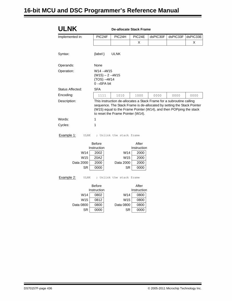
16-bit MCU and DSC Programmer’s Reference Manual
ULNK De-allocate Stack Frame
Implemented in: PIC24F PIC24H PIC24E dsPIC30F dsPIC33F dsPIC33E
X X
Syntax: {label:} ULNK
Operands: None
Operation: W14 → W15(W15) – 2 → W15(TOS) → W140 → SFA bit
Status Affected: SFA
Encoding: 1111 1010 1000 0000 0000 0000
Description: This instruction de-allocates a Stack Frame for a subroutine calling sequence. The Stack Frame is de-allocated by setting the Stack Pointer (W15) equal to the Frame Pointer (W14), and then POPping the stack to reset the Frame Pointer (W14).
Words: 1
Cycles: 1
Example 1: ULNK ; Unlink the stack frame
Before Instruction
After Instruction
W14 2002 W14 2000W15 20A2 W15 2000
Data 2000 2000 Data 2000 2000SR 0000 SR 0000
Example 2: ULNK ; Unlink the stack frame
Before Instruction
After Instruction
W14 0802 W14 0800W15 0812 W15 0800
Data 0800 0800 Data 0800 0800SR 0000 SR 0000
DS70157F-page 436 © 2005-2011 Microchip Technology Inc.

Section 5. Instruction DescriptionsInstruction
Descriptions
5
XOR Exclusive OR f and WREG
Implemented in: PIC24F PIC24H PIC24E dsPIC30F dsPIC33F dsPIC33E
X X X X X X
Syntax: {label:} XOR{.B} f {,WREG}
Operands: f ∈ [0 ... 8191]
Operation: (f).XOR.(WREG) → destination designated by D
Status Affected: N, Z
Encoding: 1011 0110 1BDf ffff ffff ffff
Description: Compute the logical exclusive OR operation of the contents of the default working register WREG and the contents of the specified file register and place the result in the destination register. The optional WREG operand determines the destination register. If WREG is specified, the result is stored in WREG. If WREG is not specified, the result is stored in the file register.
The ‘B’ bit selects byte or word operation (‘0’ for word, ‘1’ for byte).The ‘D’ bit selects the destination (‘0’ for WREG, ‘1’ for file register).The ‘f’ bits select the address of the file register.Note 1: The extension .B in the instruction denotes a byte operation
rather than a word operation. You may use a .W extension to denote a word operation, but it is not required.
2: The WREG is set to working register W0.
Words: 1
Cycles: 1(1)
Note 1: In dsPIC33E and PIC24E devices, the listed cycle count does not apply to read and read-modify-write operations on non-CPU Special Function Registers. For more details, see Note 3 in Section 3.2.1 “Multi-Cycle Instructions”.
Example 1: XOR.B 0x1FFF ; XOR (0x1FFF) and WREG (Byte mode) ; Store result to 0x1FFF
Before Instruction
After Instruction
WREG (W0) 7804 WREG (W0) 7804Data 1FFE 9439 Data 1FFE 9039
SR 0000 SR 0008 (N = 1)
Example 2: XOR 0xA04, WREG ; XOR (0xA04) and WREG (Word mode) ; Store result to WREG
Before Instruction
After Instruction
WREG (W0) 6234 WREG (W0) C267Data 0A04 A053 Data 0A04 A053
SR 0000 SR 0008 (N = 1)
© 2005-2011 Microchip Technology Inc. DS70157F-page 437
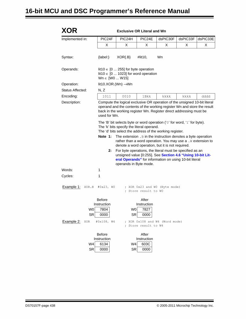
16-bit MCU and DSC Programmer’s Reference Manual
XOR Exclusive OR Literal and Wn
Implemented in: PIC24F PIC24H PIC24E dsPIC30F dsPIC33F dsPIC33E
X X X X X X
Syntax: {label:} XOR{.B} #lit10, Wn
Operands: lit10 ∈ [0 ... 255] for byte operationlit10 ∈ [0 ... 1023] for word operationWn ∈ [W0 ... W15]
Operation: lit10.XOR.(Wn) → Wn
Status Affected: N, Z
Encoding: 1011 0010 1Bkk kkkk kkkk dddd
Description: Compute the logical exclusive OR operation of the unsigned 10-bit literal operand and the contents of the working register Wn and store the result back in the working register Wn. Register direct addressing must be used for Wn.
The ‘B’ bit selects byte or word operation (‘0’ for word, ‘1’ for byte).The ‘k’ bits specify the literal operand.The ‘d’ bits select the address of the working register.Note 1: The extension .B in the instruction denotes a byte operation
rather than a word operation. You may use a .W extension to denote a word operation, but it is not required.
2: For byte operations, the literal must be specified as an unsigned value [0:255]. See Section 4.6 “Using 10-bit Lit-eral Operands” for information on using 10-bit literal operands in Byte mode.
Words: 1
Cycles: 1
Example 1: XOR.B #0x23, W0 ; XOR 0x23 and W0 (Byte mode) ; Store result to W0
Before Instruction
After Instruction
W0 7804 W0 7827SR 0000 SR 0000
Example 2: XOR #0x108, W4 ; XOR 0x108 and W4 (Word mode) ; Store result to W4
Before Instruction
After Instruction
W4 6134 W4 603CSR 0000 SR 0000
DS70157F-page 438 © 2005-2011 Microchip Technology Inc.

Section 5. Instruction DescriptionsInstruction
Descriptions
5
XOR Exclusive OR Wb and Short Literal
Implemented in: PIC24F PIC24H PIC24E dsPIC30F dsPIC33F dsPIC33E
X X X X X X
Syntax: {label:} XOR{.B} Wb, #lit5, Wd
[Wd]
[Wd++]
[Wd--]
[++Wd]
[--Wd]
Operands: Wb ∈ [W0 ... W15]lit5 ∈ [0 ... 31]Wd ∈ [W0 ... W15]
Operation: (Wb).XOR.lit5 → Wd
Status Affected: N, Z
Encoding: 0110 1www wBqq qddd d11k kkkk
Description: Compute the logical exclusive OR operation of the contents of the base register Wb and the unsigned 5-bit literal operand and place the result in the destination register Wd. Register direct addressing must be used for Wb. Either register direct or indirect addressing may be used for Wd.
The ‘w’ bits select the address of the base register.The ‘B’ bit selects byte or word operation (‘0’ for word, ‘1’ for byte).The ‘q’ bits select the destination Address mode.The ‘d’ bits select the destination register.The ‘k’ bits provide the literal operand, a 5-bit integer number.
Note: The extension .B in the instruction denotes a byte operation rather than a word operation. You may use a .W extension to denote a word operation, but it is not required.
Words: 1
Cycles: 1
Example 1: XOR.B W4, #0x14, W5 ; XOR W4 and 0x14 (Byte mode) ; Store result to W5
Before Instruction
After Instruction
W4 C822 W4 C822W5 1200 W5 1234SR 0000 SR 0000
Example 2: XOR W2, #0x1F, [W8++] ; XOR W2 by 0x1F (Word mode) ; Store result to [W8] ; Post-increment W8
Before Instruction
After Instruction
W2 8505 W2 8505W8 1004 W8 1006
Data 1004 6628 Data 1004 851ASR 0000 SR 0008 (N = 1)
© 2005-2011 Microchip Technology Inc. DS70157F-page 439

16-bit MCU and DSC Programmer’s Reference Manual
XOR Exclusive OR Wb and Ws
Implemented in: PIC24F PIC24H PIC24E dsPIC30F dsPIC33F dsPIC33E
X X X X X X
Syntax: {label:} XOR{.B} Wb, Ws, Wd
[Ws], [Wd]
[Ws++], [Wd++]
[Ws--], [Wd--]
[++Ws], [++Wd]
[--Ws], [--Wd]
Operands: Wb ∈ [W0 ... W15]Ws ∈ [W0 ... W15]Wd ∈ [W0 ... W15]
Operation: (Wb).XOR.(Ws) → Wd
Status Affected: N, Z
Encoding: 0110 1www wBqq qddd dppp ssss
Description: Compute the logical exclusive OR operation of the contents of the source register Ws and the contents of the base register Wb, and place the result in the destination register Wd. Register direct addressing must be used for Wb. Either register direct or indirect addressing may be used for Ws and Wd.
The ‘w’ bits select the address of the base register.The ‘B’ bit selects byte or word operation (‘0’ for word, ‘1’ for byte). The ‘q’ bits select the destination Address mode.The ‘d’ bits select the destination register.The ‘p’ bits select the source Address mode.The ‘s’ bits select the source register.
Note: The extension .B in the instruction denotes a byte operation rather than a word operation. You may use a .W extension to denote a word operation, but it is not required.
Words: 1
Cycles: 1(1)
Note 1: In dsPIC33E and PIC24E devices, the listed cycle count does not apply to read and read-modify-write operations on non-CPU Special Function Registers. For more details, see Note 3 in Section 3.2.1 “Multi-Cycle Instructions”.
DS70157F-page 440 © 2005-2011 Microchip Technology Inc.

Section 5. Instruction DescriptionsInstruction
Descriptions
5
Example 1: XOR.B W1, [W5++], [W9++] ; XOR W1 and [W5] (Byte mode) ; Store result to [W9] ; Post-increment W5 and W9
Before Instruction
After Instruction
W1 AAAA W1 AAAAW5 2000 W5 2001W9 2600 W9 2601
Data 2000 115A Data 2000 115AData 2600 0000 Data 2600 00F0
SR 0000 SR 0008 (N = 1)
Example 2: XOR W1, W5, W9 ; XOR W1 and W5 (Word mode) ; Store the result to W9
Before Instruction
After Instruction
W1 FEDC W1 FEDCW5 1234 W5 1234W9 A34D W9 ECE8SR 0000 SR 0008 (N = 1)
© 2005-2011 Microchip Technology Inc. DS70157F-page 441

16-bit MCU and DSC Programmer’s Reference Manual
ZE Zero-Extend Ws
Implemented in: PIC24F PIC24H PIC24E dsPIC30F dsPIC33F dsPIC33EX X X X X X
Syntax: {label:} ZE Ws, Wnd[Ws],[Ws++],[Ws--],[++Ws],[--Ws],
Operands: Ws ∈ [W0 ... W15]Wnd ∈ [W0 ... W15]
Operation: Ws<7:0> → Wnd<7:0>0 → Wnd<15:8>
Status Affected: N, Z, CEncoding: 1111 1011 1000 0ddd dppp ssss
Description: Zero-extend the Least Significant Byte in source working register Ws to a 16-bit value and store the result in the destination working register Wnd. Either register direct or indirect addressing may be used for Ws, and register direct addressing must be used for Wnd. The N flag is cleared and the C flag is set, because the zero-extended word is always positive.
The ‘d’ bits select the destination register.The ‘p’ bits select the source Address mode.The ‘s’ bits select the source register.Note 1: This operation converts a byte to a word, and it uses no .B or
.W extension.2: The source Ws is addressed as a byte operand, so any
address modification is by ‘1’.Words: 1Cycles: 1(1)
Note 1: In dsPIC33E and PIC24E devices, the listed cycle count does not apply to read and read-modify-write operations on non-CPU Special Function Registers. For more details, see Note 3 in Section 3.2.1 “Multi-Cycle Instructions”.
Example 1: ZE W3, W4 ; zero-extend W3 ; Store result to W4
Before Instruction
After Instruction
W3 7839 W3 7839W4 1005 W4 0039SR 0000 SR 0001 (C = 1)
DS70157F-page 442 © 2005-2011 Microchip Technology Inc.

Section 5. Instruction DescriptionsInstruction
Descriptions
5
Example 2: ZE [W2++], W12 ; Zero-extend [W2] ; Store to W12 ; Post-increment W2
Before Instruction
After Instruction
W2 0900 W2 0901W12 1002 W12 008F
Data 0900 268F Data 0900 268FSR 0000 SR 0001 (C = 1)
© 2005-2011 Microchip Technology Inc. DS70157F-page 443
16-bit MCU and DSC Programmer’s Reference Manual
NOTES:
DS70157F-page 444 © 2005-2011 Microchip Technology Inc.

Built-in Functio
6
Section 6. Built-in Functions
ns
HIGHLIGHTSThis section of the manual contains the following major topics:
6.1 Introduction ................................................................................................................... 4466.2 Built-in Function List...................................................................................................... 447
© 2005-2011 Microchip Technology Inc. DS70157F-page 445

16-bit MCU and DSC Programmer’s Reference Manual
6.1 INTRODUCTIONThis section describes the built-in functions that are specific to the MPLAB C Compiler for PIC24 MCUs and dsPIC DSCs (formerly MPLAB C30).
Built-in functions give the C programmer access to assembler operators or machine instructions that are currently only accessible using in-line assembly, but are sufficiently useful that they are applicable to a broad range of applications. Built-in functions are coded in C source files syntactically like function calls, but they are compiled to assembly code that directly implements the function, and do not involve function calls or library routines.
There are a number of reasons why providing built-in functions is preferable to requiring programmers to use in-line assembly. They include the following:
1. Providing built-in functions for specific purposes simplifies coding.2. Certain optimizations are disabled when in-line assembly is used. This is not the case for
built-in functions.3. For machine instructions that use dedicated registers, coding in-line assembly while
avoiding register allocation errors can require considerable care. The built-in functions make this process simpler as you do not need to be concerned with the particular register requirements for each individual machine instruction.
The built-in functions are listed below followed by their individual detailed descriptions.
This section describes only the built-in functions related to the CPU operations. The compiler provides additional built-in functions for operations such as writing to Flash program memory and changing the oscillator settings. Refer to the “MPLAB® C Compiler for PIC24 MCUs and dsPIC®
DSCs User’s Guide” (DS51284) for a complete list of compiler built-in functions.
• __builtin_addab• __builtin_add• __builtin_btg• __builtin_clr• __builtin_clr_prefetch• __builtin_divf• __builtin_divmodsd• __builtin_divmodud• __builtin_divsd• __builtin_divud• __builtin_dmaoffset• __builtin_ed• __builtin_edac• __builtin_edsoffset• __builtin_edspage• __builtin_fbcl• __builtin_lac• __builtin_mac• __builtin_modsd• __builtin_modud• __builtin_movsac• __builtin_mpy
• __builtin_mpyn• __builtin_msc• __builtin_mulss• __builtin_mulsu• __builtin_mulus• __builtin_muluu• __builtin_nop• __builtin_psvpage• __builtin_psvoffset• __builtin_readsfr• __builtin_return_address• __builtin_sac• __builtin_sacr• __builtin_sftac• __builtin_subab• __builtin_tbladdress• __builtin_tblpage• __builtin_tbloffset• __builtin_tblrdh• __builtin_tblrdl• __builtin_tblwth• __builtin_tblwtl
DS70157F-page 446 © 2005-2011 Microchip Technology Inc.

Section 6. Built-in FunctionsB
uilt-in Functions
6
6.2 BUILT-IN FUNCTION LISTThis section describes the programmer interface to the compiler built-in functions. Since the functions are “built-in”, there are no header files associated with them. Similarly, there are no command-line switches associated with the built-in functions – they are always available. The built-in function names are chosen such that they belong to the compiler’s namespace (they all have the prefix __builtin_), so they will not conflict with function or variable names in the programmer’s namespace.
__builtin_addab
Description:Add accumulators A and B with the result written back to the specified accumulator. For example:
register int result asm("A");register int B asm("A");
result = __builtin_addab(result,B);
will generate:
add A
Prototype:int __builtin_addab(int Accum_a, int Accum_b);Argument:Accum_a First accumulator to add.Accum_b Second accumulator to add.Return Value:Returns the addition result to an accumulator.Assembler Operator / Machine Instruction:add
Error Messages:An error message appears if the result is not an accumulator register.
© 2005-2011 Microchip Technology Inc. DS70157F-page 447

16-bit MCU and DSC Programmer’s Reference Manual
__builtin_add
Description:Add value to the accumulator specified by result with a shift specified by literal shift. For example:
register int result asm("A");int value;result = __builtin_add(result,value,0);
If value is held in w0, the following will be generated:
add w0, #0, A
Prototype:int __builtin_add(int Accum,int value, const int shift);
Argument:Accum Accumulator to add.value Integer number to add to accumulator value.shift Amount to shift resultant accumulator value.Return Value:Returns the shifted addition result to an accumulator.Assembler Operator / Machine Instruction:add
Error Messages:An error message appears if:
• the result is not an accumulator register• argument 0 is not an accumulator• the shift value is not a literal within range
DS70157F-page 448 © 2005-2011 Microchip Technology Inc.

Section 6. Built-in FunctionsB
uilt-in Functions
6
__builtin_btg
Description:This function will generate a btg machine instruction. Some examples include:int i; /* near by default */int l _ _attribute_ _((far));
struct foo { int bit1:1;} barbits;
int bar;
void some_bittoggles() { register int j asm("w9"); int k;
k = i;
_ _builtin_btg(&i,1); _ _builtin_btg(&j,3); _ _builtin_btg(&k,4); _ _builtin_btg(&l,11);
return j+k;}
Note that taking the address of a variable in a register will produce warning by the compiler and cause the register to be saved onto the stack (so that its address may be taken); this form is not recommended. This caution only applies to variables explicitly placed in registers by the programmer.Prototype:void _ _builtin_btg(unsigned int *, unsigned int 0xn);
Argument:* A pointer to the data item for which a bit should be toggled.0xn A literal value in the range of 0 to 15. Return Value:Returns a btg machine instruction.Assembler Operator / Machine Instruction:btg
Error Messages:An error message appears if the parameter values are not within range.
© 2005-2011 Microchip Technology Inc. DS70157F-page 449

16-bit MCU and DSC Programmer’s Reference Manual
__builtin_clr
Description:Clear the specified accumulator. For example:
register int result asm("A");result = _ _builtin_clr();
will generate:
clr A
Prototype:int _ _builtin_clr(void);
Argument:NoneReturn Value:Returns the cleared value result to an accumulator.Assembler Operator / Machine Instruction:clr
Error Messages:An error message appears if the result is not an accumulator register.
DS70157F-page 450 © 2005-2011 Microchip Technology Inc.

Section 6. Built-in FunctionsB
uilt-in Functions
6
__builtin_clr_prefetch
Description:Clear an accumulator and prefetch data ready for a future MAC operation.
xptr may be null to signify no X prefetch to be performed, in which case the values of xincrand xval are ignored, but required.
yptr may be null to signify no Y prefetch to be performed, in which case the values of yincrand yval are ignored, but required.
xval and yval nominate the address of a C variable where the prefetched value will be stored.
xincr and yincr may be the literal values: -6, -4, -2, 0, 2, 4, 6 or an integer value.
If AWB is non null, the other accumulator will be written back into the referenced variable.
For example:
register int result asm("A");register int B asm("B");int x_memory_buffer[256] _ _attribute_ _((space(xmemory)));int y_memory_buffer[256] _ _attribute_ _((space(ymemory)));int *xmemory;int *ymemory;int awb;int xVal, yVal;
xmemory = x_memory_buffer;ymemory = y_memory_buffer;result = _ _builtin_clr(&xmemory, &xVal, 2, &ymemory, &yVal, 2, &awb, B);
May generate:
clr A, [w8]+=2, w4, [w10]+=2, w5, w13
The compiler may need to spill w13 to ensure that it is available for the write-back. It may be recommended to users that the register be claimed for this purpose.
After this instruction:
• result will be cleared • xVal will contain x_memory_buffer[0] • yVal will contain y_memory_buffer[0] • xmemory and ymemory will be incremented by 2, ready for the next mac operation Prototype:int _ _builtin_clr_prefetch(int **xptr, int *xval, int xincr,int **yptr, int *yval, int yincr, int *AWB,int AWB_accum);
© 2005-2011 Microchip Technology Inc. DS70157F-page 451
16-bit MCU and DSC Programmer’s Reference Manual
Argument:xptr Integer pointer to x prefetch.xval Integer value of x prefetch.xincr Integer increment value of x prefetch.yptr Integer pointer to y prefetch.yval Integer value of y prefetch.yincr Integer increment value of y prefetch.AWB Accumulator write back location.AWB_accum Accumulator to write back.
Note: The arguments xptr and yptr must point to the arrays located in the x data memory and y data memory, respectively.
Return Value:Returns the cleared value result to an accumulator.Assembler Operator / Machine Instruction:clr
Error Messages:An error message appears if:
• the result is not an accumulator register• xval is a null value but xptr is not null• yval is a null value but yptr is not null• AWB_accum is not an accumulator and AWB is not null
__builtin_clr_prefetch (Continued)
DS70157F-page 452 © 2005-2011 Microchip Technology Inc.

Section 6. Built-in FunctionsB
uilt-in Functions
6
__builtin_divf
Description:Computes the quotient num / den. A math error exception occurs if den is zero. Function arguments are unsigned, as is the function result.Prototype:unsigned int _ _builtin_divf(unsigned int num,unsigned int den);
Argument:num numeratorden denominatorReturn Value:Returns the unsigned integer value of the quotient num / den.Assembler Operator / Machine Instruction:div.f
__builtin_divmodsd
Description:Issues the 16-bit architecture’s native signed divide support. Notably, if the quotient does not fit into a 16-bit result, the results (including remainder) are unexpected. This form of the built-in function will capture both the quotient and remainder.Prototype:signed int _ _builtin_divmodsd( signed long dividend, signed int divisor, signed int *remainder);
Argument:dividend number to be divideddivisor number to divide byremainder pointer to remainderReturn Value:Quotient and remainder.Assembler Operator / Machine Instruction:divmodsd
Error Messages:None.
© 2005-2011 Microchip Technology Inc. DS70157F-page 453

16-bit MCU and DSC Programmer’s Reference Manual
__builtin_divmodud
Description:Issues the 16-bit architecture’s native unsigned divide support. Notably, if the quotient does not fit into a 16-bit result, the results (including remainder) are unexpected. This form of the built-in function will capture both the quotient and remainder.Prototype:unsigned int _ _builtin_divmodud( unsigned long dividend, unsigned int divisor, unsigned int *remainder);
Argument:dividend number to be divideddivisor number to divide byremainder pointer to remainderReturn Value:Quotient and remainder.Assembler Operator / Machine Instruction:divmodud
Error Messages:None.
__builtin_divsd
Description:Computes the quotient num / den. A math error exception occurs if den is zero. Function arguments are signed, as is the function result. The command-line option -Wconversionscan be used to detect unexpected sign conversions.Prototype:int _ _builtin_divsd(const long num, const int den);
Argument:num numeratorden denominatorReturn Value:Returns the signed integer value of the quotient num / den.Assembler Operator / Machine Instruction:div.sd
DS70157F-page 454 © 2005-2011 Microchip Technology Inc.

Section 6. Built-in FunctionsB
uilt-in Functions
6
__builtin_divud
Description:Computes the quotient num / den. A math error exception occurs if den is zero. Function arguments are unsigned, as is the function result. The command-line option -Wconversionscan be used to detect unexpected sign conversions.Prototype:unsigned int _ _builtin_divud(const unsigned long num, const unsigned int den);
Argument:num numeratorden denominatorReturn Value:Returns the unsigned integer value of the quotient num / den.Assembler Operator / Machine Instruction:div.ud
__builtin_dmaoffset
Description:Obtains the offset of a symbol within DMA memory.
For example:
unsigned int result;char buffer[256] _ _attribute_ _((space(dma)));
result = _ _builtin_dmaoffset(&buffer);
May generate:
mov #dmaoffset(buffer), w0
Prototype:unsigned int _ _builtin_dmaoffset(const void *p);
Argument:*p pointer to DMA address valueReturn Value:Returns the offset to a variable located in DMA memory.Assembler Operator / Machine Instruction:dmaoffset
Error Messages:An error message appears if the parameter is not the address of a global symbol.
© 2005-2011 Microchip Technology Inc. DS70157F-page 455
16-bit MCU and DSC Programmer’s Reference Manual
__builtin_ed
Description:Squares sqr, returning it as the result. Also prefetches data for future square operation by computing **xptr - **yptr and storing the result in *distance.
xincr and yincr may be the literal values: -6, -4, -2, 0, 2, 4, 6 or an integer value.
For example:
register int result asm("A");int *xmemory, *ymemory;int distance;
result = _ _builtin_ed(distance, &xmemory, 2, &ymemory, 2, &distance);
May generate:
ed w4*w4, A, [w8]+=2, [W10]+=2, w4
Prototype:int _ _builtin_ed(int sqr, int **xptr, int xincr,int **yptr, int yincr, int *distance);
Argument:sqr Integer squared value.xptr Integer pointer to pointer to x prefetch.xincr Integer increment value of x prefetch.yptr Integer pointer to pointer to y prefetch.yincr Integer increment value of y prefetch.distance Integer pointer to distance.
Note: The arguments xptr and yptr must point to the arrays located in the x data memory and y data memory, respectively.
Return Value:Returns the squared result to an accumulator.
Assembler Operator / Machine Instruction:ed
Error Messages:An error message appears if:
• the result is not an accumulator register• xptr is null• yptr is null• distance is null
DS70157F-page 456 © 2005-2011 Microchip Technology Inc.

Section 6. Built-in FunctionsB
uilt-in Functions
6
__builtin_edac
Description:Squares sqr and sums with the nominated accumulator register, returning it as the result. Also prefetches data for future square operation by computing **xptr - **yptr and storing the result in *distance.
xincr and yincr may be the literal values: -6, -4, -2, 0, 2, 4, 6 or an integer value.
For example:
register int result asm("A");int *xmemory, *ymemory;int distance;
result = _ _builtin_ed(result, distance, &xmemory, 2, &ymemory, 2, &distance);
May generate:
edac w4*w4, A, [w8]+=2, [W10]+=2, w4
Prototype:int _ _builtin_edac(int Accum, int sqr, int **xptr, int xincr, int **yptr, int yincr,int *distance);
Argument:Accum Accumulator to sum.sqr Integer squared value.xptr Integer pointer to pointer to x prefetch.xincr Integer increment value of x prefetch.yptr Integer pointer to pointer to y prefetch.yincr Integer increment value of y prefetch.distance Integer pointer to distance.
Note: The arguments xptr and yptr must point to the arrays located in the x data memory and y data memory, respectively.
Return Value:Returns the squared result to specified accumulator.
Assembler Operator / Machine Instruction:edac
Error Messages:An error message appears if:
• the result is not an accumulator register• Accum is not an accumulator register• xptr is null• yptr is null• distance is null
© 2005-2011 Microchip Technology Inc. DS70157F-page 457

16-bit MCU and DSC Programmer’s Reference Manual
__builtin_edsoffset
Description:Returns the eds page offset of the object whose address is given as a parameter. The argument p must be the address of an object in extended data space; otherwise an error message is produced and the compilation fails. See the space attribute in Section 2.3.1 “Specifying Attributes of Variables” of the “MPLAB® C Compiler for PIC24 MCUs and dsPIC® DSCs User’s Guide” (DS51284).Prototype:unsigned int __builtin_edsoffset(int *p);
Argument:p object addressReturn Value:Returns the eds page number of the object whose address is given as a parameterAssembler Operator / Machine Instruction:edsoffset
__builtin_edspage
Description:Returns the eds page number of the object whose address is given as a parameter. The argument p must be the address of an object in extended data space; otherwise an error message is produced and the compilation fails. See the space attribute in Section 2.3.1 “Specifying Attributes of Variables” of the “MPLAB® C Compiler for PIC24 MCUs and dsPIC® DSCs User’s Guide” (DS51284).Prototype:unsigned int __builtin_edspage(int *p);
Argument:p object addressReturn Value:Returns the eds page number of the object whose address is given as a parameter.Assembler Operator / Machine Instruction:edspage
DS70157F-page 458 © 2005-2011 Microchip Technology Inc.
Section 6. Built-in FunctionsB
uilt-in Functions
6
__builtin_fbcl
Description:Finds the first bit change from left in value. This is useful for dynamic scaling of fixed-point data. For example:
int result, value;result = _ _builtin_fbcl(value);
May generate:
fbcl w4, w5
Prototype:int _ _builtin_fbcl(int value);
Argument:value Integer number of first bit change.Return Value:Returns the shifted addition result to an accumulator.Assembler Operator / Machine Instruction:fbcl
Error Messages:An error message appears if the result is not an accumulator register.
__builtin_lac
Description:Shifts value by shift (a literal between -8 and 7) and returns the value to be stored into the accumulator register. For example:
register int result asm("A");int value;result = _ _builtin_lac(value,3);
May generate:
lac w4, #3, A
Prototype:int _ _builtin_lac(int value, int shift);
Argument:value Integer number to be shifted.shift Literal amount to shift.Return Value:Returns the shifted addition result to an accumulator.Assembler Operator / Machine Instruction:lac
Error Messages:An error message appears if:
• the result is not an accumulator register• the shift value is not a literal within range
© 2005-2011 Microchip Technology Inc. DS70157F-page 459

16-bit MCU and DSC Programmer’s Reference Manual
__builtin_mac
Description:Computes a x b and sums with accumulator; also prefetches data ready for a future MACoperation.
xptr may be null to signify no X prefetch to be performed, in which case the values of xincrand xval are ignored, but required.
yptr may be null to signify no Y prefetch to be performed, in which case the values of yincrand yval are ignored, but required.
xval and yval nominate the address of a C variable where the prefetched value will be stored.
xincr and yincr may be the literal values: -6, -4, -2, 0, 2, 4, 6 or an integer value.
If AWB is non null, the other accumulator will be written back into the referenced variable.
For example:
register int result asm("A");register int B asm("B");int *xmemory;int *ymemory;int xVal, yVal;
result = _ _builtin_mac(result, xVal, yVal, &xmemory, &xVal, 2, &ymemory, &yVal, 2, 0, B);
May generate:
mac w4*w5, A, [w8]+=2, w4, [w10]+=2, w5
Prototype:int _ _builtin_mac(int Accum, int a, int b, int **xptr, int *xval, int xincr, int **yptr, int *yval, int yincr, int *AWB,int AWB_accum);
Argument:Accum Accumulator to sum.a Integer multiplicand.b Integer multiplier.xptr Integer pointer to pointer to x prefetch.xval Integer pointer to value of x prefetch.xincr Integer increment value of x prefetch.yptr Integer pointer to pointer to y prefetch.yval Integer pointer to value of y prefetch.yincr Integer increment value of y prefetch.AWB Accumulator write-back location.AWB_accum Accumulator to write-back.
Note: The arguments xptr and yptr must point to the arrays located in the x data memory and y data memory, respectively.
Return Value:Returns the cleared value result to an accumulator.Assembler Operator / Machine Instruction:mac
DS70157F-page 460 © 2005-2011 Microchip Technology Inc.

Section 6. Built-in FunctionsB
uilt-in Functions
6
Error Messages:An error message appears if:
• the result is not an accumulator register• Accum is not an accumulator register• xval is a null value but xptr is not null• yval is a null value but yptr is not null• AWB_accum is not an accumulator register and AWB is not null
__builtin_mac (Continued)
© 2005-2011 Microchip Technology Inc. DS70157F-page 461

16-bit MCU and DSC Programmer’s Reference Manual
__builtin_modsd
Description:Issues the 16-bit architecture’s native signed divide support. Notably, if the quotient does not fit into a 16-bit result, the results (including remainder) are unexpected. This form of the built-in function will capture only the remainder.Prototype:signed int _ _builtin_modsd(signed long dividend, signed int divisor);
Argument:dividend number to be divideddivisor number to divide byReturn Value:Remainder.Assembler Operator / Machine Instruction:modsd
Error Messages:None.
__builtin_modud
Description:Issues the 16-bit architecture’s native unsigned divide support. Notably, if the quotient does not fit into a 16-bit result, the results (including remainder) are unexpected. This form of the built-in function will capture only the remainder.Prototype:unsigned int _ _builtin_modud(unsigned long dividend, unsigned int divisor);
Argument:dividend number to be divideddivisor number to divide byReturn Value:Remainder.Assembler Operator / Machine Instruction:modud
Error Messages:None.
DS70157F-page 462 © 2005-2011 Microchip Technology Inc.
Section 6. Built-in FunctionsB
uilt-in Functions
6
__builtin_movsac
Description:Computes nothing, but prefetches data ready for a future MAC operation.
xptr may be null to signify no X prefetch to be performed, in which case the values of xincrand xval are ignored, but required.
yptr may be null to signify no Y prefetch to be performed, in which case the values of yincrand yval are ignored, but required.
xval and yval nominate the address of a C variable where the prefetched value will be stored.
xincr and yincr may be the literal values: -6, -4, -2, 0, 2, 4, 6 or an integer value.
If AWB is not null, the other accumulator will be written back into the referenced variable.
For example:
register int result asm("A");int *xmemory;int *ymemory;int xVal, yVal;
result = _ _builtin_movsac(&xmemory, &xVal, 2, &ymemory, &yVal, 2, 0, 0);
May generate:
movsac A, [w8]+=2, w4, [w10]+=2, w5
Prototype:int _ _builtin_movsac(int **xptr, int *xval, int xincr,int **yptr, int *yval, int yincr, int *AWBint AWB_accum);
Argument:xptr Integer pointer to pointer to x prefetch.xval Integer pointer to value of x prefetch.xincr Integer increment value of x prefetch.yptr Integer pointer to pointer to y prefetch.yval Integer pointer to value of y prefetch.yincr Integer increment value of y prefetch.AWB Accumulator write back location.AWB_accum Accumulator to write back.
Note: The arguments xptr and yptr must point to the arrays located in the x data memory and y data memory, respectively.
Return Value:Returns prefetch data.Assembler Operator / Machine Instruction:movsac
Error Messages:An error message appears if:
• the result is not an accumulator register• xval is a null value but xptr is not null• yval is a null value but yptr is not null• AWB_accum is not an accumulator register and AWB is not null
© 2005-2011 Microchip Technology Inc. DS70157F-page 463

16-bit MCU and DSC Programmer’s Reference Manual
__builtin_mpy
Description:Computes a x b ; also prefetches data ready for a future MAC operation.
xptr may be null to signify no X prefetch to be performed, in which case the values of xincrand xval are ignored, but required.
yptr may be null to signify no Y prefetch to be performed, in which case the values of yincrand yval are ignored, but required.
xval and yval nominate the address of a C variable where the prefetched value will be stored.
xincr and yincr may be the literal values: -6, -4, -2, 0, 2, 4, 6 or an integer value.
For example:
register int result asm("A");int *xmemory;int *ymemory;int xVal, yVal;
result = _ _builtin_mpy(xVal, yVal, &xmemory, &xVal, 2, &ymemory, &yVal, 2);
May generate:
mac w4*w5, A, [w8]+=2, w4, [w10]+=2, w5
Prototype:int _ _builtin_mpy(int a, int b,int **xptr, int *xval, int xincr,int **yptr, int *yval, int yincr);
Argument:a Integer multiplicand.b Integer multiplier.xptr Integer pointer to pointer to x prefetch.xval Integer pointer to value of x prefetch.xincr Integer increment value of x prefetch.yptr Integer pointer to pointer to y prefetch.yval Integer pointer to value of y prefetch.yincr Integer increment value of y prefetch.AWB Integer pointer to accumulator selection.
Note: The arguments xptr and yptr must point to the arrays located in the x data memory and y data memory, respectively.
Return Value:Returns the cleared value result to an accumulator.Assembler Operator / Machine Instruction:mpy
Error Messages:An error message appears if:
• the result is not an accumulator register• xval is a null value but xptr is not null• yval is a null value but yptr is not null
DS70157F-page 464 © 2005-2011 Microchip Technology Inc.

Section 6. Built-in FunctionsB
uilt-in Functions
6
__builtin_mpyn
Description:Computes -a x b ; also prefetches data ready for a future MAC operation.
xptr may be null to signify no X prefetch to be performed, in which case the values of xincrand xval are ignored, but required.
yptr may be null to signify no Y prefetch to be performed, in which case the values of yincrand yval are ignored, but required.
xval and yval nominate the address of a C variable where the prefetched value will be stored.
xincr and yincr may be the literal values: -6, -4, -2, 0, 2, 4, 6 or an integer value.
For example:
register int result asm("A");int *xmemory;int *ymemory;int xVal, yVal;
result = _ _builtin_mpy(xVal, yVal, &xmemory, &xVal, 2, &ymemory, &yVal, 2);
May generate:
mac w4*w5, A, [w8]+=2, w4, [w10]+=2, w5
Prototype:int _ _builtin_mpyn(int a, int b,int **xptr, int *xval, int xincr,int **yptr, int *yval, int yincr);
Argument:a Integer multiplicand.b Integer multiplier.xptr Integer pointer to pointer to x prefetch.xval Integer pointer to value of x prefetch.xincr Integer increment value of x prefetch.yptr Integer pointer to pointer to y prefetch.yval Integer pointer to value of y prefetch.yincr Integer increment value of y prefetch.AWB Integer pointer to accumulator selection.
Note: The arguments xptr and yptr must point to the arrays located in the x data memory and y data memory, respectively.
Return Value:Returns the cleared value result to an accumulator.Assembler Operator / Machine Instruction:mpyn
Error Messages:An error message appears if:
• the result is not an accumulator register• xval is a null value but xptr is not null• yval is a null value but yptr is not null
© 2005-2011 Microchip Technology Inc. DS70157F-page 465

16-bit MCU and DSC Programmer’s Reference Manual
__builtin_msc
Description:Computes a x b and subtracts from accumulator; also prefetches data ready for a future MACoperation.
xptr may be null to signify no X prefetch to be performed, in which case the values of xincrand xval are ignored, but required.
yptr may be null to signify no Y prefetch to be performed, in which case the values of yincrand yval are ignored, but required.
xval and yval nominate the address of a C variable where the prefetched value will be stored.
xincr and yincr may be the literal values: -6, -4, -2, 0, 2, 4, 6 or an integer value.
If AWB is non null, the other accumulator will be written back into the referenced variable.
For example:
register int result asm("A");int *xmemory;int *ymemory;int xVal, yVal;
result = _ _builtin_msc(result, xVal, yVal, &xmemory, &xVal, 2, &ymemory, &yVal, 2, 0, 0);May generate: msc w4*w5, A, [w8]+=2, w4, [w10]+=2, w5
Prototype:int _ _builtin_msc(int Accum, int a, int b, int **xptr, int *xval, int xincr, int **yptr, int *yval, int yincr, int *AWB,int AWB_accum);
Argument:Accum IAccumulator to sum.a Integer multiplicand.b Integer multiplier.xptr Integer pointer to pointer to x prefetch.xval Integer pointer to value of x prefetch.xincr Integer increment value of x prefetch.yptr Integer pointer to pointer to y prefetch.yval Integer pointer to value of y prefetch.yincr Integer increment value of y prefetch.AWB Accumulator write back location.AWB_accum Accumulator to write back.
Note: The arguments xptr and yptr must point to the arrays located in the x data memory and y data memory, respectively.
Return Value:Returns the cleared value result to an accumulator.Assembler Operator / Machine Instruction:msc
DS70157F-page 466 © 2005-2011 Microchip Technology Inc.

Section 6. Built-in FunctionsB
uilt-in Functions
6
Error Messages:An error message appears if:
• the result is not an accumulator register• Accum is not an accumulator register• xval is a null value but xptr is not null• yval is a null value but yptr is not null• AWB_accum is not an accumulator register and AWB is not null
__builtin_msc (Continued)
© 2005-2011 Microchip Technology Inc. DS70157F-page 467

16-bit MCU and DSC Programmer’s Reference Manual
__builtin_mulss
Description:Computes the product p0 x p1. Function arguments are signed integers, and the function result is a signed long integer. The command-line option -Wconversions can be used to detect unexpected sign conversions.Prototype:signed long _ _builtin_mulss(const signed int p0, const signed int p1);
Argument:p0 multiplicandp1 multiplierReturn Value:Returns the signed long integer value of the product p0 x p1.Assembler Operator / Machine Instruction:mul.ss
__builtin_mulsu
Description:Computes the product p0 x p1. Function arguments are integers with mixed signs, and the function result is a signed long integer. The command-line option -Wconversions can be used to detect unexpected sign conversions. This function supports the full range of addressing modes of the instruction, including immediate mode for operand p1.Prototype:signed long _ _builtin_mulsu(const signed int p0, const unsigned int p1);
Argument:p0 multiplicandp1 multiplierReturn Value:Returns the signed long integer value of the product p0 x p1.Assembler Operator / Machine Instruction:mul.su
DS70157F-page 468 © 2005-2011 Microchip Technology Inc.

Section 6. Built-in FunctionsB
uilt-in Functions
6
__builtin_mulus
Description:Computes the product p0 x p1. Function arguments are integers with mixed signs, and the function result is a signed long integer. The command-line option -Wconversions can be used to detect unexpected sign conversions. This function supports the full range of addressing modes of the instruction.Prototype:signed long _ _builtin_mulus(const unsigned int p0, const signed int p1);
Argument:p0 multiplicandp1 multiplierReturn Value:Returns the signed long integer value of the product p0 x p1.Assembler Operator / Machine Instruction:mul.us
__builtin_muluu
Description:Computes the product p0 x p1. Function arguments are unsigned integers, and the function result is an unsigned long integer. The command-line option -Wconversions can be used to detect unexpected sign conversions. This function supports the full range of addressing modes of the instruction, including immediate mode for operand p1.Prototype:unsigned long _ _builtin_muluu(const unsigned int p0, const unsigned int p1);
Argument:p0 multiplicandp1 multiplierReturn Value:Returns the signed long integer value of the product p0 x p1.Assembler Operator / Machine Instruction:mul.uu
© 2005-2011 Microchip Technology Inc. DS70157F-page 469

16-bit MCU and DSC Programmer’s Reference Manual
__builtin_nop
Description:Generates a nop instruction.Prototype:void _ _builtin_nop(void);
Argument:None.Return Value:Returns a no operation (nop).Assembler Operator / Machine Instruction:nop
__builtin_psvoffset
Description:Returns the psv page offset of the object whose address is given as a parameter. The argument p must be the address of an object in an EE data, PSV or executable memory space; otherwise an error message is produced and the compilation fails. See the space attribute in Section 2.3.1 “Specifying Attributes of Variables” of the “MPLAB® C Compiler for PIC24 MCUs and dsPIC® DSCs User’s Guide” (DS51284).Prototype:unsigned int _ _builtin_psvoffset(const void *p);
Argument:p object addressReturn Value:Returns the psv page number offset of the object whose address is given as a parameter.Assembler Operator / Machine Instruction:psvoffset
Error Messages:The following error message is produced when this function is used incorrectly:
“Argument to _ _builtin_psvoffset() is not the address of an object in code, psv, or eedata section”.
The argument must be an explicit object address.
For example, if obj is object in an executable or read-only section, the following syntax is valid:
unsigned page = _ _builtin_psvoffset(&obj);
DS70157F-page 470 © 2005-2011 Microchip Technology Inc.

Section 6. Built-in FunctionsB
uilt-in Functions
6
__builtin_psvpage
Description:Returns the psv page number of the object whose address is given as a parameter. The argument p must be the address of an object in an EE data, PSV or executable memory space; otherwise an error message is produced and the compilation fails. See the space attribute in Section 2.3.1 “Specifying Attributes of Variables” of the “MPLAB® C Compiler for PIC24 MCUs and dsPIC® DSCs User’s Guide” (DS51284).Prototype:unsigned int _ _builtin_psvpage(const void *p);
Argument:p object addressReturn Value:Returns the psv page number of the object whose address is given as a parameter.Assembler Operator / Machine Instruction:psvpage
Error Messages:The following error message is produced when this function is used incorrectly:
“Argument to _ _builtin_psvpage() is not the address of an object in code, psv, or eedata section”.
The argument must be an explicit object address.
For example, if obj is object in an executable or read-only section, the following syntax is valid:
unsigned page = _ _builtin_psvpage(&obj);
__builtin_readsfr
Description:Reads the SFR.Prototype:unsigned int _ _builtin_readsfr(const void *p);
Argument:p object addressReturn Value:Returns the SFR.Assembler Operator / Machine Instruction:readsfr
Error Messages:The following error message is produced when this function is used incorrectly:
© 2005-2011 Microchip Technology Inc. DS70157F-page 471

16-bit MCU and DSC Programmer’s Reference Manual
__builtin_return_address
Description:Returns the return address of the current function, or of one of its callers. For the levelargument, a value of 0 yields the return address of the current function, a value of 1 yields the return address of the caller of the current function, and so forth. When level exceeds the current stack depth, 0 will be returned. This function should only be used with a non-zero argument for debugging purposes.Prototype:int _ _builtin_return_address (const int level);
Argument:level Number of frames to scan up the call stack.Return Value:Returns the return address of the current function, or of one of its callers.Assembler Operator / Machine Instruction:return_address
__builtin_sac
Description:Shifts value by shift (a literal between -8 and 7) and returns the value.
For example:
register int value asm("A");int result;
result = _ _builtin_sac(value,3);
May generate:
sac A, #3, w0
Prototype:int _ _builtin_sac(int value, int shift);
Argument:value Integer number to be shifted.shift Literal amount to shift.Return Value:Returns the shifted result to an accumulator.Assembler Operator / Machine Instruction:sac
Error Messages:An error message appears if:
• the result is not an accumulator register• the shift value is not a literal within range
DS70157F-page 472 © 2005-2011 Microchip Technology Inc.

Section 6. Built-in FunctionsB
uilt-in Functions
6
__builtin_sacr
Description:Shifts value by shift (a literal between -8 and 7) and returns the value which is rounded using the rounding mode determined by the CORCONbits.RND control bit.
For example:
register int value asm("A");int result;
result = _ _builtin_sac(value,3);
May generate:
sac.r A, #3, w0
Prototype:int _ _builtin_sacr(int value, int shift);
Argument:value Integer number to be shifted.shift Literal amount to shift.Return Value:Returns the shifted result to the CORCON register.Assembler Operator / Machine Instruction:sacr
Error Messages:An error message appears if:
• the result is not an accumulator register• the shift value is not a literal within range
© 2005-2011 Microchip Technology Inc. DS70157F-page 473

16-bit MCU and DSC Programmer’s Reference Manual
__builtin_sftac
Description:Shifts accumulator by shift. The valid shift range is -16 to 16.
For example:
register int result asm("A");int i;
result = _ _builtin_sftac(result,i);
May generate:
sftac A, w0
Prototype:int _ _builtin_sftac(int Accum, int shift);
Argument:Accum Accumulator to shift.shift Amount to shift.Return Value:Returns the shifted result to an accumulator.Assembler Operator / Machine Instruction:sftac
Error Messages:An error message appears if:
• the result is not an accumulator register• Accum is not an accumulator register• the shift value is not a literal within range
DS70157F-page 474 © 2005-2011 Microchip Technology Inc.
Section 6. Built-in FunctionsB
uilt-in Functions
6
__builtin_subab
Description:Subtracts accumulators A and B with the result written back to the specified accumulator. For example:
register int result asm("A");register int B asm("B"); result = _ _builtin_subab(result,B);
will generate:
sub A
Prototype:int _ ___builtin_subab(int Accum_a, int Accum_b);Argument:Accum_a Accumulator from which to subtract.Accum_b Accumulator to subtract.Return Value:Returns the subtraction result to an accumulator.Assembler Operator / Machine Instruction:sub
Error Messages:An error message appears if the result is not an accumulator register.
__builtin_tbladdress
Description:Returns a value that represents the address of an object in program memory. The argument pmust be the address of an object in an EE data, PSV or executable memory space; otherwise an error message is produced and the compilation fails. See the space attribute in Section 2.3.1 “Specifying Attributes of Variables” of the “MPLAB® C Compiler for PIC24 MCUs and dsPIC® DSCs User’s Guide” (DS51284).Prototype:unsigned long _ _builtin_tblpage(const void *p);
Argument:p object addressReturn Value:Returns an unsigned long value that represents the address of an object in program memory.Assembler Operator / Machine Instruction:tbladdress
© 2005-2011 Microchip Technology Inc. DS70157F-page 475

16-bit MCU and DSC Programmer’s Reference Manual
Error Messages:The following error message is produced when this function is used incorrectly:
“Argument to _ _builtin_tbladdress() is not the address of an object in code, psv, or eedata section”.
The argument must be an explicit object address.
For example, if obj is object in an executable or read-only section, the following syntax is valid:
unsigned long page = _ _builtin_tbladdress(&obj);
__builtin_tbloffset
Description:Returns the table page offset of the object whose address is given as a parameter. The argument p must be the address of an object in an EE data, PSV or executable memory space; otherwise an error message is produced and the compilation fails. See the space attribute in Section 2.3.1 “Specifying Attributes of Variables” of the “MPLAB® C Compiler for PIC24 MCUs and dsPIC® DSCs User’s Guide” (DS51284).Prototype:unsigned int _ _builtin_tbloffset(const void *p);
Argument:p object addressReturn Value:Returns the table page number offset of the object whose address is given as a parameter.Assembler Operator / Machine Instruction:tbloffset
Error Messages:The following error message is produced when this function is used incorrectly:
“Argument to _ _builtin_tbloffset() is not the address of an object in code, psv, or eedata section”.
The argument must be an explicit object address.
For example, if obj is object in an executable or read-only section, the following syntax is valid:
unsigned page = _ _builtin_tbloffset(&obj);
__builtin_tbladdress
DS70157F-page 476 © 2005-2011 Microchip Technology Inc.

Section 6. Built-in FunctionsB
uilt-in Functions
6
__builtin_tblpage
Description:Returns the table page number of the object whose address is given as a parameter. The argument p must be the address of an object in an EE data, PSV or executable memory space; otherwise an error message is produced and the compilation fails. See the space attribute in Section 2.3.1 “Specifying Attributes of Variables” of the “MPLAB® C Compiler for PIC24 MCUs and dsPIC® DSCs User’s Guide” (DS51284).Prototype:unsigned int _ _builtin_tblpage(const void *p);
Argument:p object addressReturn Value:Returns the table page number of the object whose address is given as a parameter.Assembler Operator / Machine Instruction:tblpage
Error Messages:The following error message is produced when this function is used incorrectly:
“Argument to _ _builtin_tblpage() is not the address of an object in code, psv, or eedata section”.
The argument must be an explicit object address.
For example, if obj is object in an executable or read-only section, the following syntax is valid:
unsigned page = _ _builtin_tblpage(&obj);
__builtin_tblrdh
Description:Issues the tblrdh.w instruction to read a word from Flash or EEDATA memory. You must set up the TBLPAG to point to the appropriate page. To do this, you may make use of _ _builtin_tbloffset() and _ _builtin_tblpage().
Please refer to the specific device data sheet or the appropriate family reference manual for complete details regarding reading and writing program Flash.Prototype:unsigned int _ _builtin_tblrdh(unsigned int offset);
Argument:offset desired memory offsetReturn Value:None.Assembler Operator / Machine Instruction:tblrdh
Error Messages:None.
© 2005-2011 Microchip Technology Inc. DS70157F-page 477

16-bit MCU and DSC Programmer’s Reference Manual
__builtin_tblrdl
Description:Issues the tblrdl.w instruction to read a word from Flash or EEDATA memory. You must set up the TBLPAG to point to the appropriate page. To do this, you may make use of _ _builtin_tbloffset() and_ _builtin_tblpage().
Please refer to the specific device data sheet or the appropriate family reference manual for complete details regarding reading and writing program Flash.Prototype:unsigned int _ _builtin_tblrdl(unsigned int offset);
Argument:offset desired memory offsetReturn Value:None.Assembler Operator / Machine Instruction:tblrdl
Error Messages:None.
__builtin_tblwth
Description:Issues the tblwth.w instruction to write a word to Flash or EEDATA memory. You must set up the TBLPAG to point to the appropriate page. To do this, you may make use of _ _builtin_tbloffset() and _ _builtin_tblpage().
Please refer to the specific device data sheet or the appropriate family reference manual for complete details regarding reading and writing program Flash.Prototype:void _ _builtin_tblwth(unsigned int offset unsigned int data);
Argument:offset desired memory offsetdata data to be writtenReturn Value:None.Assembler Operator / Machine Instruction:tblwth
Error Messages:None.
DS70157F-page 478 © 2005-2011 Microchip Technology Inc.

Section 6. Built-in FunctionsB
uilt-in Functions
6
__builtin_tblwtl
Description:Issues the tblrdl.w instruction to write a word to Flash or EEDATA memory. You must set up the TBLPAG to point to the appropriate page. To do this, you may make use of _ _builtin_tbloffset() and _ _builtin_tblpage().
Please refer to the specific device data sheet or the appropriate family reference manual for complete details regarding reading and writing program Flash.Prototype:void _ _builtin_tblwtl(unsigned int offset unsigned int data);
Argument:offset desired memory offsetdata data to be writtenReturn Value:None.Assembler Operator / Machine Instruction:tblwtl
Error Messages:None.
© 2005-2011 Microchip Technology Inc. DS70157F-page 479

16-bit MCU and DSC Programmer’s Reference Manual
Example 6-1: Additional Inline Functions #include "p33fxxxx.h"
volatile long Result_mpy1616;volatile long Result_addab;volatile long Result_subab;volatile long Result_mpy3216;volatile long Result_div3216;
register int Accu_A asm("A");register int Accu_B asm("B");
inline static long mpy_32_16 (long, int);
inline static long mpy_32_16 (long x, int y){
long result;int temp1, temp2;temp1 = (x>>1)&0x7FFF;temp2 = x>>16;Accu_A = __builtin_mpy (temp1, y, 0,0,0,0,0,0);Accu_A = __builtin_sftac (15);Accu_A = __builtin_mac (temp2, y, 0,0,0,0,0,0,0);
asm("mov _ACCAL,%0\n\t" "mov _ACCAH,%d0" : "=r"(result) : "w"(Accu_A));
return result;}
int main (void){
// Variable declarationsint Input1;int Input2;int Input3;int Input4;long Input5;int Input6;long Input7;int Input8;
// Enable 32-bit saturation, signed and fractional modes for both ACCA and ACCB
CORCON = 0x00C0;
// Example of 16*16-bit fractional multiplication using ACCAInput1 = 32767;Input2 = 32767;Accu_A = __builtin_mpy (Input1, Input2, 0,0,0,0,0,0);asm("mov _ACCAL,%0\n\t""mov _ACCAH,%d0" : "=r"(Result_mpy1616) : "w"(Accu_A));
// Example of 16*16-bit fractional multiplication using ACCBInput3 = 16384;Input4 = 16384;Accu_B = __builtin_mpy (Input3, Input4, 0,0,0,0,0,0);asm("mov _ACCBL,%0\n\t""mov _ACCBH,%d0" : "=r"(Result_mpy1616) : "w"(Accu_B));
// Example of 32-bit addition using ACCA (ACCA = ACCA + ACCB)Accu_A = __builtin_addab();asm("mov _ACCAL,%0\n\t""mov _ACCAH,%d0" : "=r"(Result_addab) : "w"(Accu_A));
// Example of 32-bit subtraction using ACCB (ACCB = ACCB - ACCA)Accu_B = __builtin_subab();asm("mov _ACCBL,%0\n\t""mov _ACCBH,%d0" : "=r"(Result_subab) : "w"(Accu_B));
// Example of 32*16-bit fractional multiplication using ACCAInput5 = 0x7FFFFFFF;Input6 = 32767;Result_mpy3216 = mpy_32_16 (Input5, Input6);
while(1);}
DS70157F-page 480 © 2005-2011 Microchip Technology Inc.
Section 6. Built-in FunctionsB
uilt-in Functions
6
Example 6-2: Divide_32_by_16#include <p33Fxxxx.h>#include "divide.h"_FOSCSEL(FNOSC_FRC);_FOSC(FCKSM_CSDCMD & OSCIOFNC_OFF & POSCMD_NONE);_FWDT(FWDTEN_OFF);
unsigned int divide_(long a, int b) { union convert {
unsigned long l;unsigned int i[2];
} c;
int sign; unsigned int result; c.l = a; sign = c.i[1] ^ b;
if (a < 0) a = (-a); if (b < 0) b = -b; result = __builtin_divud(a,b); result >>= 1; if (sign < 0) result = -result; return result;}
int main(void){
unsigned long dividend;unsigned int divisor;unsigned int quotient;
dividend = 0x3FFFFFFF;divisor = 0x7FFF;
quotient = divide_((long)dividend, (int)divisor);while(1);
}
© 2005-2011 Microchip Technology Inc. DS70157F-page 481

16-bit MCU and DSC Programmer’s Reference Manual
NOTES:
DS70157F-page 482 © 2005-2011 Microchip Technology Inc.

Section 7. Reference
Reference
7
HIGHLIGHTSThis section of the manual contains the following major topics:
7.1 Instruction Bit Map ........................................................................................................ 4847.2 Instruction Set Summary Table ..................................................................................... 4867.3 Revision History ............................................................................................................ 496
© 2005-2011 Microchip Technology Inc. DS70157F-page 483
16-bit MCU and DSC Programmer’s Reference Manual
7.1 INSTRUCTION BIT MAPInstruction encoding for the 16-bit MCU and DSC family devices is summarized in Table 7-1. This table contains the encoding for the MSB of each instruction. The first column in the table represents bits 23:20 of the opcode, and the first row of the table represents bits 19:16 of the opcode. The first byte of the opcode is formed by taking the first column bit value and appending the first row bit value. For instance, the MSB of the PUSH instruction (last row, ninth column) is encoded with 11111000b (0xF8).
Note: The complete opcode for each instruction may be determined by the instruction descriptions in Section 5. “Instruction Descriptions”, using Table 5-1 through Table 5-12.
DS70157F-page 484 © 2005-2011 Microchip Technology Inc.

© 2005-2011 M
icrochip Technology Inc.D
S70157F-page 485
Section 7. Reference
R 7
Ta
011 1100 1101 1110 1111
Opc
ode<
23:2
0>
— BRA(1)
(OA)BRA(1)
(OB)BRA(1)
(SA)BRA(1)
(SB)
UBBR
RANN)
BRA(GT)
BRA(GE)
BRA(GTU)
—
ADDC
SUBB
XOR
MOV
TST BTSTS BSW BTSS BTSC
LWTHLWTL
MUL SUBSUBB
MOV.D MOV
D(1)
G(1)
B(1)
SAC(1) SAC.R(1) — FF1LFF1R
— — SL ASRLSR
FBCL
LRETM
INCINC2
DECDEC2
COMNEG
CLRSETM
SEZE
DISI DAWEXCHSWAP
CLRWDTMOVPAG(2)
PWRSAVPOP.S
PUSH.SRESET
NOPR
No
eference
ble 7-1: Instruction EncodingOpcode<19:16>
0000 0001 0010 0011 0100 0101 0110 0111 1000 1001 1010 1
0000 NOP BRACALLGOTORCALL
CALL — GOTO RETLW RETFIERETURN
RCALL DO(1) REPEAT —
0001 SUBR S0010 MOV0011 BRA
(OV)BRA (C)
BRA(Z)
BRA(N)
BRA(LE)
BRA(LT)
BRA(LEU)
BRA BRA (NOV) BRA(NC)
BRA(NZ)
B(
0100 ADD0101 SUB0110 AND0111 IOR1000 MOV1001 MOV1010 BSET BCLR BTG BTST BTSTS BTST BTSS BTSC BSET BCLR BTG B1011 ADD
ADDCSUB
SUBBANDXOR
IORMOV
ADDADDC
SUBSUBB
ANDXOR
IORMOV
MUL.USMUL.UU
MUL.SSMUL.SU
TBLRDHTBLRDL
TBTB
1100 MAC(1)
MPY(1)
MPY.N(1)
MSC(1)
CLRAC(1) MAC(1)
MPY(1)
MPY.N(1)
MSC(1)
MOVSAC(1) SFTAC(1) ADD(1) LAC(1) ADNESU
1101 SL ASRLSR
RLCRLNC
RRC RRNC
SL ASRLSR
RLC RLNC
RRC RRNC
DIV.SDIV.U
DIVF(1) —
1110 CP0 CPCPB
CP0 CPCPB
— — CPBGT(2)
CPBLT(2)
CPSGTCPSLT
CPBEQ(2)
CPBNE(2)
CPSEQCPSNE
INCINC2
DECDEC2
COMNEG
CS
1111 ED(1)
EDAC(1)
MAC(1)
MPY(1)
— — — — PUSH POP LNKULNK
te 1: This instruction is only available in dsPIC30F, dsPIC33F, and dsPIC33E family devices.2: This instruction is only available in PIC24E and dsPIC33E family devices.

16-bit MC
U and D
SC Program
mer’s R
eference Manual
DS
70157F-page 486©
2005-2011 Microchip Technology Inc.
is table contains an alphabetized listing of the execution time (in instruction cycles), affected 1-2 identifies the symbols that are used in the
dsPIC33F devices. Some instructions require truction Set Summary Tables” and Section
B(2) SAB(1,2) DC N OV Z C Page Number
— 99
— 100
— 101
— 102
— — — — — 103
— — — — — 104
— 106
— 107
— 108
— 110
— — — — 112
— — — — 113
— — — — 114
— — — — 115
— — — 117
— — — 119
— — — — 121
7.2 INSTRUCTION SET SUMMARY TABLEThe complete 16-bit MCU and DSC device instruction set is summarized in Table 7-2. Thinstruction set. It includes instruction assembly syntax, description, size (in 24-bit words),Status bits, and the page number in which the detailed description can be found. Table Instruction Set Summary Table.
Note: The instruction cycle counts listed here are for PIC24F, PIC24H, dsPIC30F andadditional cycles in PIC24E and dsPIC33E devices. Refer to Section 3.3 “Ins5.4 “Instruction Descriptions” for details.
Table 7-2: Instruction Set Summary Table Assembly Syntax
Mnemonic, Operands Description Words Cycles OA(2) OB(2) SA(1,2) SB(1,2) OA
ADD f {,WREG} Destination = f + WREG 1 1 — — — — —
ADD #lit10,Wn Wn = lit10 + Wn 1 1 — — — — —
ADD Wb,#lit5,Wd Wd = Wb + lit5 1 1 — — — — —
ADD Wb,Ws,Wd Wd = Wb + Ws 1 1 — — — — —
ADD Acc(2) Add accumulators 1 1
ADD Wso,#Slit4,Acc 16-bit signed add to accumulator 1 1
ADDC f {,WREG} Destination = f + WREG + (C) 1 1 — — — — —
ADDC #lit10,Wn Wn = lit10 + Wn + (C) 1 1 — — — — —
ADDC Wb,#lit5,Wd Wd = Wb + lit5 + (C) 1 1 — — — — —
ADDC Wb,Ws,Wd Wd = Wb + Ws + (C) 1 1 — — — — —
AND f {,WREG} Destination = f .AND. WREG 1 1 — — — — —
AND #lit10,Wn Wn = lit10 .AND. Wn 1 1 — — — — —
AND Wb,#lit5,Wd Wd = Wb .AND. lit5 1 1 — — — — —
AND Wb,Ws,Wd Wd = Wb .AND. Ws 1 1 — — — — —
ASR f {,WREG} Destination = arithmetic right shift f, LSb → C 1 1 — — — — —
ASR Ws,Wd Wd = arithmetic right shift Ws, LSb → C 1 1 — — — — —
ASR Wb,#lit4,Wnd Wnd = arithmetic right shift Wb by lit4, LSb → C 1 1 — — — — —
Legend: set or cleared; may be cleared, but never set; may be set, but never cleared; ‘1’ always set; ‘0’ always cleared; — unchangedNote 1: SA, SB and SAB are only modified if the corresponding saturation is enabled, otherwise unchanged.
2: This instruction/operand is only available in dsPIC30F, dsPIC33F, and dsPIC33E devices.3: This instruction/operand is only available in PIC24E and dsPIC33E devices.4: This instruction/operand is only available in dsPIC33E devices.5: This instruction/operand is only available in PIC24F, PIC24H, dsPIC30F, and dsPIC33F devices.6: This instruction/operand is only available in dsPIC30F and dsPIC33F devices.
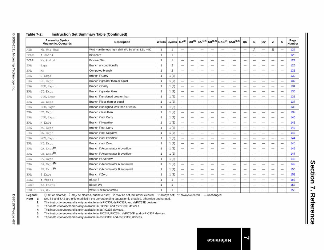
© 2005-2011 M
icrochip Technology Inc.D
S70157F-page 487
Section 7. Reference
R 7
AS — — — — 122
BC — — — — — — 123
BC — — — — — — 124
BR — — — — — — 126
BR — — — — — — 128
BR — — — — — — 130
BR — — — — — — 132
BR — — — — — — 134
BR — — — — — — 135
BR — — — — — — 136
BR — — — — — — 137
BR — — — — — — 138
BR — — — — — — 139
BR — — — — — — 140
BR — — — — — — 141
BR — — — — — — 142
BR — — — — — — 143
BR — — — — — — 144
BR — — — — — — 145
BR — — — — — — 146
BR — — — — — — 147
BR — — — — — — 148
BR — — — — — — 149
BR — — — — — — 150
BR — — — — — — 151
BS — — — — — — 152
BS — — — — — — 153
BS — — — — — — 155
Ta
SAB(1,2) DC N OV Z C Page Number
LeNo
eference
R Wb,Wns,Wnd Wnd = arithmetic right shift Wb by Wns, LSb → C 1 1 — — — — —
LR f,#bit4 Bit clear f 1 1 — — — — —
LR Ws,#bit4 Bit clear Ws 1 1 — — — — —
A Expr Branch unconditionally 1 2 — — — — —
A Wn Computed branch 1 2 — — — — —
A C,Expr Branch if Carry 1 1 (2) — — — — —
A GE,Expr Branch if greater than or equal 1 1 (2) — — — — —
A GEU,Expr Branch if Carry 1 1 (2) — — — — —
A GT,Expr Branch if greater than 1 1 (2) — — — — —
A GTU,Expr Branch if unsigned greater than 1 1 (2) — — — — —
A LE,Expr Branch if less than or equal 1 1 (2) — — — — —
A LEU,Expr Branch if unsigned less than or equal 1 1 (2) — — — — —
A LT,Expr Branch if less than 1 1 (2) — — — — —
A LTU,Expr Branch if not Carry 1 1 (2) — — — — —
A N,Expr Branch if Negative 1 1 (2) — — — — —
A NC,Expr Branch if not Carry 1 1 (2) — — — — —
A NN,Expr Branch if not Negative 1 1 (2) — — — — —
A NOV,Expr Branch if not Overflow 1 1 (2) — — — — —
A NZ,Expr Branch if not Zero 1 1 (2) — — — — —
A OA,Expr(2) Branch if Accumulator A overflow 1 1 (2) — — — — —
A OB,Expr(2) Branch if Accumulator B overflow 1 1 (2) — — — — —
A OV,Expr Branch if Overflow 1 1 (2) — — — — —
A SA,Expr(2) Branch if Accumulator A saturated 1 1 (2) — — — — —
A SB,Expr(2) Branch if Accumulator B saturated 1 1 (2) — — — — —
A Z,Expr Branch if Zero 1 1 (2) — — — — —
ET f,#bit4 Bit set f 1 1 — — — — —
ET Ws,#bit4 Bit set Ws 1 1 — — — — —
W.C Ws,Wb Write C bit to Ws<Wb> 1 1 — — — — —
ble 7-2: Instruction Set Summary Table (Continued)Assembly Syntax
Mnemonic, Operands Description Words Cycles OA(2) OB(2) SA(1,2) SB(1,2) OAB(2)
gend: set or cleared; may be cleared, but never set; may be set, but never cleared; ‘1’ always set; ‘0’ always cleared; — unchangedte 1: SA, SB and SAB are only modified if the corresponding saturation is enabled, otherwise unchanged.
2: This instruction/operand is only available in dsPIC30F, dsPIC33F, and dsPIC33E devices.3: This instruction/operand is only available in PIC24E and dsPIC33E devices.4: This instruction/operand is only available in dsPIC33E devices.5: This instruction/operand is only available in PIC24F, PIC24H, dsPIC30F, and dsPIC33F devices.6: This instruction/operand is only available in dsPIC30F and dsPIC33F devices.

16-bit MC
U and D
SC Program
mer’s R
eference Manual
DS
70157F-page 488©
2005-2011 Microchip Technology Inc.
— — — — — — 155
— — — — — — 157
— — — — — — 158
— — — — — — 160
— — — — — — 162
— — — — — — 164
— — — — — — 166
— — — — — 168
— — — — — 169
— — — — — 169
— — — — — 171
— — — — — 171
— — — — — 173
— — — — — 175
— — — — — 175
— — — — — — 177
— — — — — — 180
— — — — — — 183
— — — — — — 184
— — — — — — 184
— — — — — — 185
0 — — — — — 186
— — — — — — 188
— — — — 189
— — — — 190
B(2) SAB(1,2) DC N OV Z C Page Number
BSW.Z Ws,Wb Write Z bit to Ws<Wb> 1 1 — — — — —
BTG f,#bit4 Bit toggle f 1 1 — — — — —
BTG Ws,#bit4 Bit toggle Ws 1 1 — — — — —
BTSC f,#bit4 Bit test f, skip if clear 1 1(2 or 3) — — — — —
BTSC Ws,#bit4 Bit test Ws, skip if clear 1 1(2 or 3) — — — — —
BTSS f,#bit4 Bit test f, skip if set 1 1(2 or 3) — — — — —
BTSS Ws,#bit4 Bit test Ws, skip if set 1 1(2 or 3) — — — — —
BTST f,#bit4 Bit test f to Z 1 1 — — — — —
BTST.C Ws,#bit4 Bit test Ws to C 1 1 — — — — —
BTST.Z Ws,#bit4 Bit test Ws to Z 1 1 — — — — —
BTST.C Ws,Wb Bit test Ws<Wb> to C 1 1 — — — — —
BTST.Z Ws,Wb Bit test Ws<Wb> to Z 1 1 — — — — —
BTSTS f,#bit4 Bit test f to Z, then set f 1 1 — — — — —
BTSTS.C Ws,#bit4 Bit test Ws to C then set 1 1 — — — — —
BTSTS.Z Ws,#bit4 Bit test Ws to Z then set 1 1 — — — — —
CALL Expr Call subroutine 2 2 — — — — —
CALL Wn Call indirect subroutine 1 2 — — — — —
CALL.L Wn(3) Call indirect subroutine (long address) 1 4 — — — — —
CLR f f = 0x0000 1 1 — — — — —
CLR WREG WREG = 0x0000 1 1 — — — — —
CLR Wd Wd = 0 1 1 — — — — —
CLR Acc,[Wx],Wxd,[Wy],Wyd,AWB(2) Clear accumulator 1 1 0 0 0 0 0
CLRWDT Clear Watchdog Timer 1 1 — — — — —
COM f {,WREG} Destination = f 1 1 — — — — —
COM Ws,Wd Wd = Ws 1 1 — — — — —
Table 7-2: Instruction Set Summary Table (Continued)Assembly Syntax
Mnemonic, Operands Description Words Cycles OA(2) OB(2) SA(1,2) SB(1,2) OA
Legend: set or cleared; may be cleared, but never set; may be set, but never cleared; ‘1’ always set; ‘0’ always cleared; — unchangedNote 1: SA, SB and SAB are only modified if the corresponding saturation is enabled, otherwise unchanged.
2: This instruction/operand is only available in dsPIC30F, dsPIC33F, and dsPIC33E devices.3: This instruction/operand is only available in PIC24E and dsPIC33E devices.4: This instruction/operand is only available in dsPIC33E devices.5: This instruction/operand is only available in PIC24F, PIC24H, dsPIC30F, and dsPIC33F devices.6: This instruction/operand is only available in dsPIC30F and dsPIC33F devices.

© 2005-2011 M
icrochip Technology Inc.D
S70157F-page 489
Section 7. Reference
R 7
CP — 191
CP — 192
CP — 193
CP — 194
CP — 1 1 196
CP — 1 1 197
CP — 198
CP — 199
CP — 200
CP — 201
CP — — — — — — 203
CP — — — — — — 204
CP — — — — — — 205
CP — — — — — — 206
CP — — — — — — 207
CP — — — — — — 211
CP — — — — — — 212
CP — — — — — — 214
DA — — — — — 216
DE — 217
DE — 218
DE — 220
DE — 221
Ta
SAB(1,2) DC N OV Z C Page Number
LeNo
eference
f Compare (f – WREG) 1 1 — — — — —
Wb,#lit5 Compare (Wb – lit5) 1 1 — — — — —
Wb,#lit8 Compare (Wb – lit8) 1 1 — — — — —
Wb,Ws Compare (Wb – Ws) 1 1 — — — — —
0 f Compare (f – 0x0000) 1 1 — — — — —
0 Ws Compare (Ws – 0x0000) 1 1 — — — — —
B f Compare with borrow (f – WREG – C) 1 1 — — — — —
B Wb,#lit5 Compare with borrow (Wb – lit5 – C) 1 1 — — — — —
B Wb,#lit8 Compare with borrow (Wb – lit8 – C) 1 1 — — — — —
B Wb,Ws Compare with borrow (Wb – Ws – C) 1 1 — — — — —
BEQ Wb,Wn,Expr(3) Compare Wb with Wn, branch if = 1 1 (5) — — — — —
BGT Wb,Wn,Expr(3) Signed Compare Wb with Wn, branch if > 1 1 (5) — — — — —
BLT Wb,Wn,Expr(3) Signed Compare Wb with Wn, branch if < 1 1 (5) — — — — —
BNE Wb,Wn,Expr(3) Compare Wb with Wn, branch if ≠ 1 1 (5) — — — — —
SEQ Wb,Wn Compare (Wb with Wn), skip if = 1 1(2 or 3) — — — — —
SGT Wb,Wn Signed Compare (Wb with Wn), skip if > 1 1(2 or 3) — — — — —
SLT Wb,Wn Signed Compare (Wb with Wn), skip if < 1 1(2 or 3) — — — — —
SNE Wb,Wn Compare (Wb with Wn), skip if ≠ 1 1(2 or 3) — — — — —
W.B Wn Wn = decimal adjust Wn 1 1 — — — — —
C f {,WREG} Destination = f – 1 1 1 — — — — —
C Ws,Wd Wd = Ws – 1 1 1 — — — — —
C2 f {,WREG} Destination = f – 2 1 1 — — — — —
C2 Ws,Wd Wd = Ws – 2 1 1 — — — — —
ble 7-2: Instruction Set Summary Table (Continued)Assembly Syntax
Mnemonic, Operands Description Words Cycles OA(2) OB(2) SA(1,2) SB(1,2) OAB(2)
gend: set or cleared; may be cleared, but never set; may be set, but never cleared; ‘1’ always set; ‘0’ always cleared; — unchangedte 1: SA, SB and SAB are only modified if the corresponding saturation is enabled, otherwise unchanged.
2: This instruction/operand is only available in dsPIC30F, dsPIC33F, and dsPIC33E devices.3: This instruction/operand is only available in PIC24E and dsPIC33E devices.4: This instruction/operand is only available in dsPIC33E devices.5: This instruction/operand is only available in PIC24F, PIC24H, dsPIC30F, and dsPIC33F devices.6: This instruction/operand is only available in dsPIC30F and dsPIC33F devices.

16-bit MC
U and D
SC Program
mer’s R
eference Manual
DS
70157F-page 490©
2005-2011 Microchip Technology Inc.
— — — — — — 223
— — 224
— — 224
— — 0 0 226
— — 0 226
— — 228
— — — — — — 230
— — — — — — 233
— — — — — — 235
— — — — — 239
— — — — — 241
— — — — — — 243
— — — — — 244
— — — — — 246
— — — — — 248
— — — — — — 250
— — — — — — 251
— — — — — — 253
— 254
— 255
— 257
— 258
— — — — 260
— — — — 261
— — — — 262
— — — — 263
— — — — — 265
B(2) SAB(1,2) DC N OV Z C Page Number
DISI #lit14 Disable interrupts for lit14 instruction cycles 1 1 — — — — —
DIV.S Wm,Wn Signed 16/16-bit integer divide, Q → Wo, R → W1 1 18 — — — — —
DIV.SD Wm,Wn Signed 32/16-bit integer divide, Q → Wo, R → W1 1 18 — — — — —
DIV.U Wm,Wn Unsigned 16/16-bit integer divide, Q → Wo, R → W1 1 18 — — — — —
DIV.UD Wm,Wn Unsigned 32/16-bit integer divide, Q → Wo, R → W1 1 18 — — — — —
DIVF Wm,Wn(2) Signed 16/16-bit fractional divide, Q → Wo, R → W1 1 18 — — — — —
DO #lit14,Expr(6) Do code to PC + Expr, (lit14 + 1) times 2 2 — — — — —
DO #lit15,Expr(4) Do code to PC + Expr, (lit15 + 1) times 2 2 — — — — —
DO Wn,Expr(2) Do code to PC + Expr, (Wn + 1) times 2 2 — — — — —
ED Wm*Wm,Acc,[Wx],[Wy],Wxd(2) Euclidean distance (no accumulate) 1 1
EDAC Wm*Wm,Acc,[Wx],[Wy],Wxd(2) Euclidean distance 1 1
EXCH Wns,Wnd Swap Wns and Wnd 1 1 — — — — —
FBCL Ws,Wnd Find bit change from left (MSb) side 1 1 — — — — —
FF1L Ws,Wnd Find first one from left (MSb) side 1 1 — — — — —
FF1R Ws,Wnd Find first one from right (LSb) side 1 1 — — — — —
GOTO Expr Go to address 2 2 — — — — —
GOTO Wn Go to address indirectly 1 2 — — — — —
GOTO.L Wn(3) Go to address indirectly (long address) 1 4 — — — — —
INC f {,WREG} Destination = f + 1 1 1 — — — — —
INC Ws,Wd Wd = Ws + 1 1 1 — — — — —
INC2 f {,WREG} Destination = f + 2 1 1 — — — — —
INC2 Ws,Wd Wd = Ws + 2 1 1 — — — — —
IOR f {,WREG} Destination = f .IOR. WREG 1 1 — — — — —
IOR #lit10,Wn Wn = lit10 .IOR. Wn 1 1 — — — — —
IOR Wb,#lit5,Wd Wd = Wb .IOR. lit5 1 1 — — — — —
IOR Wb,Ws,Wd Wd = Wb .IOR. Ws 1 1 — — — — —
LAC Wso,#Slit4, Acc(2) Load accumulator 1 1
Table 7-2: Instruction Set Summary Table (Continued)Assembly Syntax
Mnemonic, Operands Description Words Cycles OA(2) OB(2) SA(1,2) SB(1,2) OA
Legend: set or cleared; may be cleared, but never set; may be set, but never cleared; ‘1’ always set; ‘0’ always cleared; — unchangedNote 1: SA, SB and SAB are only modified if the corresponding saturation is enabled, otherwise unchanged.
2: This instruction/operand is only available in dsPIC30F, dsPIC33F, and dsPIC33E devices.3: This instruction/operand is only available in PIC24E and dsPIC33E devices.4: This instruction/operand is only available in dsPIC33E devices.5: This instruction/operand is only available in PIC24F, PIC24H, dsPIC30F, and dsPIC33F devices.6: This instruction/operand is only available in dsPIC30F and dsPIC33F devices.
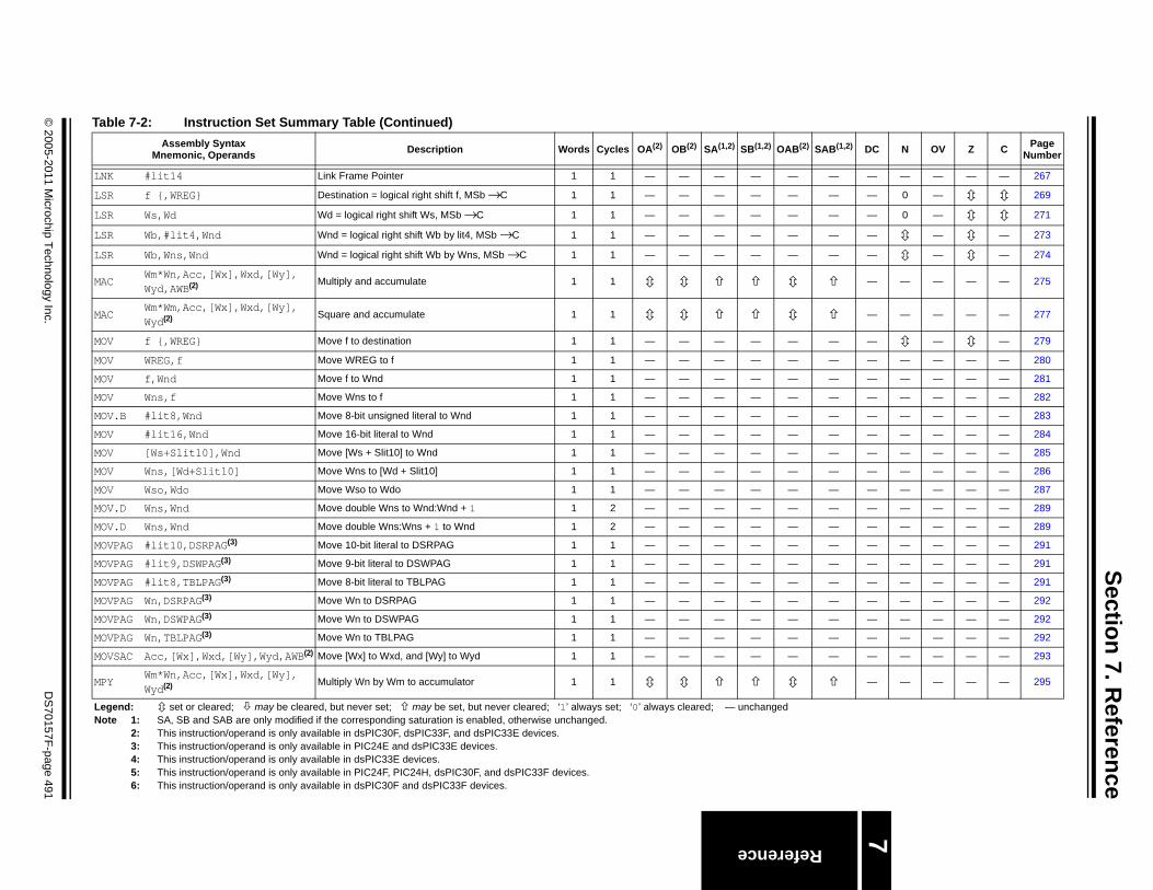
© 2005-2011 M
icrochip Technology Inc.D
S70157F-page 491
Section 7. Reference
R 7
LN — — — — — — 267
LS — — 0 — 269
LS — — 0 — 271
LS — — — — 273
LS — — — — 274
MA — — — — — 275
MA — — — — — 277
MO — — — — 279
MO — — — — — — 280
MO — — — — — — 281
MO — — — — — — 282
MO — — — — — — 283
MO — — — — — — 284
MO — — — — — — 285
MO — — — — — — 286
MO — — — — — — 287
MO — — — — — — 289
MO — — — — — — 289
MO — — — — — — 291
MO — — — — — — 291
MO — — — — — — 291
MO — — — — — — 292
MO — — — — — — 292
MO — — — — — — 292
MO — — — — — — 293
MP — — — — — 295
Ta
SAB(1,2) DC N OV Z C Page Number
LeNo
eference
K #lit14 Link Frame Pointer 1 1 — — — — —
R f {,WREG} Destination = logical right shift f, MSb → C 1 1 — — — — —
R Ws,Wd Wd = logical right shift Ws, MSb → C 1 1 — — — — —
R Wb,#lit4,Wnd Wnd = logical right shift Wb by lit4, MSb → C 1 1 — — — — —
R Wb,Wns,Wnd Wnd = logical right shift Wb by Wns, MSb → C 1 1 — — — — —
CWm*Wn,Acc,[Wx],Wxd,[Wy], Wyd,AWB(2) Multiply and accumulate 1 1
CWm*Wm,Acc,[Wx],Wxd,[Wy], Wyd(2) Square and accumulate 1 1
V f {,WREG} Move f to destination 1 1 — — — — —
V WREG,f Move WREG to f 1 1 — — — — —
V f,Wnd Move f to Wnd 1 1 — — — — —
V Wns,f Move Wns to f 1 1 — — — — —
V.B #lit8,Wnd Move 8-bit unsigned literal to Wnd 1 1 — — — — —
V #lit16,Wnd Move 16-bit literal to Wnd 1 1 — — — — —
V [Ws+Slit10],Wnd Move [Ws + Slit10] to Wnd 1 1 — — — — —
V Wns,[Wd+Slit10] Move Wns to [Wd + Slit10] 1 1 — — — — —
V Wso,Wdo Move Wso to Wdo 1 1 — — — — —
V.D Wns,Wnd Move double Wns to Wnd:Wnd + 1 1 2 — — — — —
V.D Wns,Wnd Move double Wns:Wns + 1 to Wnd 1 2 — — — — —
VPAG #lit10,DSRPAG(3) Move 10-bit literal to DSRPAG 1 1 — — — — —
VPAG #lit9,DSWPAG(3) Move 9-bit literal to DSWPAG 1 1 — — — — —
VPAG #lit8,TBLPAG(3) Move 8-bit literal to TBLPAG 1 1 — — — — —
VPAG Wn,DSRPAG(3) Move Wn to DSRPAG 1 1 — — — — —
VPAG Wn,DSWPAG(3) Move Wn to DSWPAG 1 1 — — — — —
VPAG Wn,TBLPAG(3) Move Wn to TBLPAG 1 1 — — — — —
VSAC Acc,[Wx],Wxd,[Wy],Wyd,AWB(2) Move [Wx] to Wxd, and [Wy] to Wyd 1 1 — — — — —
YWm*Wn,Acc,[Wx],Wxd,[Wy], Wyd(2) Multiply Wn by Wm to accumulator 1 1
ble 7-2: Instruction Set Summary Table (Continued)Assembly Syntax
Mnemonic, Operands Description Words Cycles OA(2) OB(2) SA(1,2) SB(1,2) OAB(2)
gend: set or cleared; may be cleared, but never set; may be set, but never cleared; ‘1’ always set; ‘0’ always cleared; — unchangedte 1: SA, SB and SAB are only modified if the corresponding saturation is enabled, otherwise unchanged.
2: This instruction/operand is only available in dsPIC30F, dsPIC33F, and dsPIC33E devices.3: This instruction/operand is only available in PIC24E and dsPIC33E devices.4: This instruction/operand is only available in dsPIC33E devices.5: This instruction/operand is only available in PIC24F, PIC24H, dsPIC30F, and dsPIC33F devices.6: This instruction/operand is only available in dsPIC30F and dsPIC33F devices.
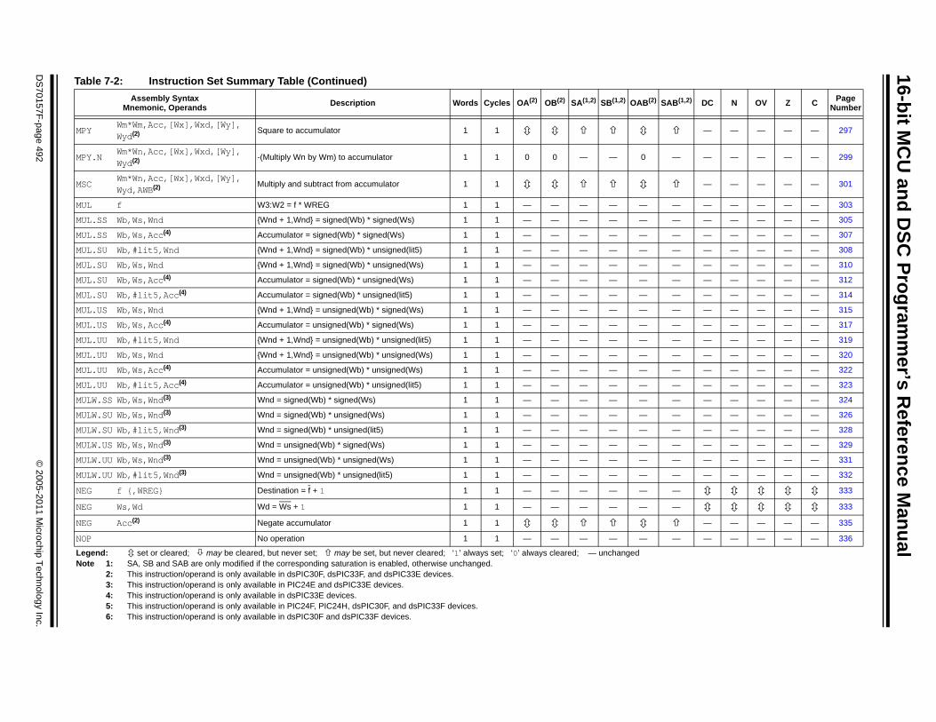
16-bit MC
U and D
SC Program
mer’s R
eference Manual
DS
70157F-page 492©
2005-2011 Microchip Technology Inc.
— — — — — 297
— — — — — — 299
— — — — — 301
— — — — — — 303
— — — — — — 305
— — — — — — 307
— — — — — — 308
— — — — — — 310
— — — — — — 312
— — — — — — 314
— — — — — — 315
— — — — — — 317
— — — — — — 319
— — — — — — 320
— — — — — — 322
— — — — — — 323
— — — — — — 324
— — — — — — 326
— — — — — — 328
— — — — — — 329
— — — — — — 331
— — — — — — 332
— 333
— 333
— — — — — 335
— — — — — — 336
B(2) SAB(1,2) DC N OV Z C Page Number
MPYWm*Wm,Acc,[Wx],Wxd,[Wy], Wyd(2) Square to accumulator 1 1
MPY.NWm*Wn,Acc,[Wx],Wxd,[Wy], Wyd(2) -(Multiply Wn by Wm) to accumulator 1 1 0 0 — — 0
MSCWm*Wn,Acc,[Wx],Wxd,[Wy], Wyd,AWB(2) Multiply and subtract from accumulator 1 1
MUL f W3:W2 = f * WREG 1 1 — — — — —
MUL.SS Wb,Ws,Wnd {Wnd + 1,Wnd} = signed(Wb) * signed(Ws) 1 1 — — — — —
MUL.SS Wb,Ws,Acc(4) Accumulator = signed(Wb) * signed(Ws) 1 1 — — — — —
MUL.SU Wb,#lit5,Wnd {Wnd + 1,Wnd} = signed(Wb) * unsigned(lit5) 1 1 — — — — —
MUL.SU Wb,Ws,Wnd {Wnd + 1,Wnd} = signed(Wb) * unsigned(Ws) 1 1 — — — — —
MUL.SU Wb,Ws,Acc(4) Accumulator = signed(Wb) * unsigned(Ws) 1 1 — — — — —
MUL.SU Wb,#lit5,Acc(4) Accumulator = signed(Wb) * unsigned(lit5) 1 1 — — — — —
MUL.US Wb,Ws,Wnd {Wnd + 1,Wnd} = unsigned(Wb) * signed(Ws) 1 1 — — — — —
MUL.US Wb,Ws,Acc(4) Accumulator = unsigned(Wb) * signed(Ws) 1 1 — — — — —
MUL.UU Wb,#lit5,Wnd {Wnd + 1,Wnd} = unsigned(Wb) * unsigned(lit5) 1 1 — — — — —
MUL.UU Wb,Ws,Wnd {Wnd + 1,Wnd} = unsigned(Wb) * unsigned(Ws) 1 1 — — — — —
MUL.UU Wb,Ws,Acc(4) Accumulator = unsigned(Wb) * unsigned(Ws) 1 1 — — — — —
MUL.UU Wb,#lit5,Acc(4) Accumulator = unsigned(Wb) * unsigned(lit5) 1 1 — — — — —
MULW.SS Wb,Ws,Wnd(3) Wnd = signed(Wb) * signed(Ws) 1 1 — — — — —
MULW.SU Wb,Ws,Wnd(3) Wnd = signed(Wb) * unsigned(Ws) 1 1 — — — — —
MULW.SU Wb,#lit5,Wnd(3) Wnd = signed(Wb) * unsigned(lit5) 1 1 — — — — —
MULW.US Wb,Ws,Wnd(3) Wnd = unsigned(Wb) * signed(Ws) 1 1 — — — — —
MULW.UU Wb,Ws,Wnd(3) Wnd = unsigned(Wb) * unsigned(Ws) 1 1 — — — — —
MULW.UU Wb,#lit5,Wnd(3) Wnd = unsigned(Wb) * unsigned(lit5) 1 1 — — — — —
NEG f {,WREG} Destination = f + 1 1 1 — — — — —
NEG Ws,Wd Wd = Ws + 1 1 1 — — — — —
NEG Acc(2) Negate accumulator 1 1
NOP No operation 1 1 — — — — —
Table 7-2: Instruction Set Summary Table (Continued)Assembly Syntax
Mnemonic, Operands Description Words Cycles OA(2) OB(2) SA(1,2) SB(1,2) OA
Legend: set or cleared; may be cleared, but never set; may be set, but never cleared; ‘1’ always set; ‘0’ always cleared; — unchangedNote 1: SA, SB and SAB are only modified if the corresponding saturation is enabled, otherwise unchanged.
2: This instruction/operand is only available in dsPIC30F, dsPIC33F, and dsPIC33E devices.3: This instruction/operand is only available in PIC24E and dsPIC33E devices.4: This instruction/operand is only available in dsPIC33E devices.5: This instruction/operand is only available in PIC24F, PIC24H, dsPIC30F, and dsPIC33F devices.6: This instruction/operand is only available in dsPIC30F and dsPIC33F devices.

© 2005-2011 M
icrochip Technology Inc.D
S70157F-page 493
Section 7. Reference
R 7
NO — — — — — — 336
PO — — — — — — 337
PO — — — — — — 338
PO — — — — — — 339
PO — 340
PU — — — — — — 341
PU — — — — — — 342
PU — — — — — — 343
PU — — — — — — 345
PW — — — — — — 346
RC — — — — — — 347
RC — — — — — — 351
RE — — — — — — 355
RE — — — — — — 357
RE — — — — — — 359
RE — — — — — — 363
RE — — 365
RE — — — — — — 367
RE — — — — — — 371
RL — — — 373
RL — — — 375
RL — — — — 377
RL — — — — 379
RR — — — 381
RR — — — 383
RR — — — — 385
RR — — — — 387
SA — — — — — — 389
Ta
SAB(1,2) DC N OV Z C Page Number
LeNo
eference
PR No operation 1 1 — — — — —
P f POP TOS to f 1 1 — — — — —
P Wdo POP TOS to Wdo 1 1 — — — — —
P.D Wnd POP double from TOS to Wnd:Wnd + 1 1 2 — — — — —
P.S POP shadow registers 1 1 — — — — —
SH f PUSH f to TOS 1 1 — — — — —
SH Wso PUSH Wso to TOS 1 1 — — — — —
SH.D Wns PUSH double Wns:Wns + 1 to TOS 1 2 — — — — —
SH.S PUSH shadow registers 1 1 — — — — —
RSAV #lit1 Enter Power-saving mode 1 1 — — — — —
ALL Expr Relative call 1 2 — — — — —
ALL Wn Computed call 1 2 — — — — —
PEAT #lit14(5) Repeat next instruction (lit14 + 1) times 1 1 — — — — —
PEAT #lit15(3) Repeat next instruction (lit15 + 1) times 1 1 — — — — —
PEAT Wn Repeat next instruction (Wn + 1) times 1 1 — — — — —
SET Software device Reset 1 1 — — — — —
TFIE Return from interrupt enable 1 3 (2) — — — — —
TLW #lit10,Wn Return with lit10 in Wn 1 3 (2) — — — — —
TURN Return from subroutine 1 3 (2) — — — — —
C f {,WREG} Destination = rotate left through Carry f 1 1 — — — — —
C Ws,Wd Wd = rotate left through Carry Ws 1 1 — — — — —
NC f {,WREG} Destination = rotate left (no Carry) f 1 1 — — — — —
NC Ws,Wd Wd = rotate left (no Carry) Ws 1 1 — — — — —
C f {,WREG} Destination = rotate right through Carry f 1 1 — — — — —
C Ws,Wd Wd = rotate right through Carry Ws 1 1 — — — — —
NC f {,WREG} Destination = rotate right (no Carry) f 1 1 — — — — —
NC Ws,Wd Wd = rotate right (no Carry) Ws 1 1 — — — — —
C Acc,#Slit4,Wdo(2) Store accumulator 1 1 — — — — —
ble 7-2: Instruction Set Summary Table (Continued)Assembly Syntax
Mnemonic, Operands Description Words Cycles OA(2) OB(2) SA(1,2) SB(1,2) OAB(2)
gend: set or cleared; may be cleared, but never set; may be set, but never cleared; ‘1’ always set; ‘0’ always cleared; — unchangedte 1: SA, SB and SAB are only modified if the corresponding saturation is enabled, otherwise unchanged.
2: This instruction/operand is only available in dsPIC30F, dsPIC33F, and dsPIC33E devices.3: This instruction/operand is only available in PIC24E and dsPIC33E devices.4: This instruction/operand is only available in dsPIC33E devices.5: This instruction/operand is only available in PIC24F, PIC24H, dsPIC30F, and dsPIC33F devices.6: This instruction/operand is only available in dsPIC30F and dsPIC33F devices.

16-bit MC
U and D
SC Program
mer’s R
eference Manual
DS
70157F-page 494©
2005-2011 Microchip Technology Inc.
— — — — — — 391
— — — 393
— — — — — — 395
— — — — — — 395
— — — — — — 396
— — — — — 397
— — — — — 398
— — — 399
— — — 401
— — — — 403
— — — — 404
— 405
— 406
— 407
— 408
— — — — — 410
— 411
— 412
— 413
— 415
— 417
— 418
— 420
— 422
— 423
— 424
— — — — — — 426
B(2) SAB(1,2) DC N OV Z C Page Number
SAC.R Acc,#Slit4,Wdo(2) Store rounded Accumulator 1 1 — — — — —
SE Ws,Wd Wd = sign-extended Ws 1 1 — — — — —
SETM f f = 0xFFFF 1 1 — — — — —
SETM WREG WREG = 0xFFFF 1 1 — — — — —
SETM Wd Wd = 0xFFFF 1 1 — — — — —
SFTAC Acc,#Slit6(2) Arithmetic shift accumulator by Slit6 1 1
SFTAC Acc,Wb(2) Arithmetic shift accumulator by (Wb) 1 1
SL f {,WREG} Destination = arithmetic left shift f 1 1 — — — — —
SL Ws,Wd Wd = arithmetic left shift Ws 1 1 — — — — —
SL Wb,#lit4,Wnd Wnd = left shift Wb by lit4 1 1 — — — — —
SL Wb,Wns,Wnd Wnd = left shift Wb by Wns 1 1 — — — — —
SUB f {,WREG} Destination = f – WREG 1 1 — — — — —
SUB #lit10,Wn Wn = Wn – lit10 1 1 — — — — —
SUB Wb,#lit5,Wd Wd = Wb – lit5 1 1 — — — — —
SUB Wb,Ws,Wd Wd = Wb – Ws 1 1 — — — — —
SUB Acc(2) Subtract accumulators 1 1
SUBB f {,WREG} destination = f – WREG – (C) 1 1 — — — — —
SUBB #lit10,Wn Wn = Wn – lit10 – (C) 1 1 — — — — —
SUBB Wb,#lit5,Wd Wd = Wb – lit5 – (C) 1 1 — — — — —
SUBB Wb,Ws,Wd Wd = Wb – Ws – (C) 1 1 — — — — —
SUBBR f {,WREG} Destination = WREG – f – (C) 1 1 — — — — —
SUBBR Wb,#lit5,Wd Wd = lit5 – Wb – (C) 1 1 — — — — —
SUBBR Wb,Ws,Wd Wd = Ws – Wb – (C) 1 1 — — — — —
SUBR f {,WREG} Destination = WREG – f 1 1 — — — — —
SUBR Wb,#lit5,Wd Wd = lit5 – Wb 1 1 — — — — —
SUBR Wb,Ws,Wd Wd = Ws – Wb 1 1 — — — — —
SWAP Wn Wn = byte or nibble swap Wn 1 1 — — — — —
Table 7-2: Instruction Set Summary Table (Continued)Assembly Syntax
Mnemonic, Operands Description Words Cycles OA(2) OB(2) SA(1,2) SB(1,2) OA
Legend: set or cleared; may be cleared, but never set; may be set, but never cleared; ‘1’ always set; ‘0’ always cleared; — unchangedNote 1: SA, SB and SAB are only modified if the corresponding saturation is enabled, otherwise unchanged.
2: This instruction/operand is only available in dsPIC30F, dsPIC33F, and dsPIC33E devices.3: This instruction/operand is only available in PIC24E and dsPIC33E devices.4: This instruction/operand is only available in dsPIC33E devices.5: This instruction/operand is only available in PIC24F, PIC24H, dsPIC30F, and dsPIC33F devices.6: This instruction/operand is only available in dsPIC30F and dsPIC33F devices.

© 2005-2011 M
icrochip Technology Inc.D
S70157F-page 495
Section 7. Reference
R 7
TB — — — — — — 427
TB — — — — — — 429
TB — — — — — — 431
TB — — — — — — 433
UL — — — — — — 435
XO — — — — 437
XO — — — — 438
XO — — — — 439
XO — — — — 440
ZE — — 0 — 1 442
Ta
SAB(1,2) DC N OV Z C Page Number
LeNo
eference
LRDH [Ws],Wd Read high program word to Wd 1 2 — — — — —
LRDL [Ws],Wd Read low program word to Wd 1 2 — — — — —
LWTH Ws,[Wd] Write Ws to high program word 1 2 — — — — —
LWTL Ws,[Wd] Write Ws to low program word 1 2 — — — — —
NK Unlink Frame Pointer 1 1 — — — — —
R f {,WREG} Destination = f .XOR. WREG 1 1 — — — — —
R #lit10,Wn Wn = lit10 .XOR. Wn 1 1 — — — — —
R Wb,#lit5,Wd Wd = Wb .XOR. lit5 1 1 — — — — —
R Wb,Ws,Wd Wd = Wb .XOR. Ws 1 1 — — — — —
Ws,Wnd Wnd = zero-extended Ws 1 1 — — — — —
ble 7-2: Instruction Set Summary Table (Continued)Assembly Syntax
Mnemonic, Operands Description Words Cycles OA(2) OB(2) SA(1,2) SB(1,2) OAB(2)
gend: set or cleared; may be cleared, but never set; may be set, but never cleared; ‘1’ always set; ‘0’ always cleared; — unchangedte 1: SA, SB and SAB are only modified if the corresponding saturation is enabled, otherwise unchanged.
2: This instruction/operand is only available in dsPIC30F, dsPIC33F, and dsPIC33E devices.3: This instruction/operand is only available in PIC24E and dsPIC33E devices.4: This instruction/operand is only available in dsPIC33E devices.5: This instruction/operand is only available in PIC24F, PIC24H, dsPIC30F, and dsPIC33F devices.6: This instruction/operand is only available in dsPIC30F and dsPIC33F devices.
16-bit MCU and DSC Programmer’s Reference Manual
7.3 REVISION HISTORY
Revision A (May 2005)This is the initial release of this document.
Revision B (September 2005)This revision incorporates all known errata at the time of this document update.
Revision C (February 2008)This revision includes the following corrections and updates:
• Instruction Updates:- Updated BRA Instruction (see “BRA”)- Updated DIVF Instruction (see “DIVF”)- Updated DO Instruction (see “DO”)- Updated SUB instruction (see “SUB”)
Revision D (November 2009)This revision includes the following corrections and updates:
• Document renamed from dsPIC30F/33F Programmer’s Reference Manual to 16-bit MCU and DSC Programmer’s Reference Manual
• Document has been completely redesigned to accommodate all current 16-bit families: dsPIC30F, dsPIC33F, PIC24F and PIC24H
Revision E (June 2010)This revision includes the following corrections and updates:
• Information specific to dsPIC33E and PIC24E devices has been added throughout the document
Revision F (July 2011)This revision includes the following corrections and updates:
• Added a new section “Built-in Functions”• Added and updated the cross-references throughout the document• Updated the bit characteristics from U to U-0 in Register 2-4 and Register 2-6• Added a note throughout the document specifying the requirement of an additional cycle for
read and read-modify-write operations on non-CPU special function registers in dsPIC33E and PIC24E devices
• Updates to formatting and minor text changes were incorporated throughout the document
DS70157F-page 496 © 2005-2011 Microchip Technology Inc.

IndexIndex
INDEXSymbols__builtin_addab................................................................. 447__builtin_btg.............................................................. 447, 448__builtin_divmodud ........................................................... 454__builtin_divsd .................................................................. 454__builtin_edsoffset ............................................................ 458__builtin_edspage............................................................. 458__builtin_mac.................................................................... 460__builtin_modsd................................................................ 462__builtin_modud................................................................ 462__builtin_mpy.................................................................... 464__builtin_mpyn.................................................................. 465__builtin_mulss ................................................................. 468__builtin_muluu................................................................. 469__builtin_nop..................................................................... 470__builtin_psvoffset ............................................................ 470__builtin_sac ..................................................................... 472__builtin_subab................................................................. 475__builtin_tbladdress .......................................................... 475__builtin_tblwth ................................................................. 478__builtin_tblwtl .................................................................. 479
AAccumulator A, Accumulator B ........................................... 19Accumulator Access ........................................................... 84Accumulator Selection ........................................................ 97Accumulator Usage............................................................. 83Addressing Modes for Wd Destination Register ................. 95Addressing Modes for Ws Source Register ........................ 95Assigned Working Register Usage ..................................... 78
BBuilt-In Functions
__builtin_addab......................................................... 447__builtin_btg...................................................... 447, 448__builtin_divmodud ................................................... 454__builtin_divsd .......................................................... 454__builtin_edsoffset .................................................... 458__builtin_edspage..................................................... 458__builtin_mac............................................................ 460__builtin_modsd........................................................ 462__builtin_modud........................................................ 462__builtin_mpy............................................................ 464__builtin_mpyn.......................................................... 465__builtin_mulss ......................................................... 468__builtin_muluu......................................................... 469__builtin_nop............................................................. 470__builtin_psvoffset .................................................... 470__builtin_sac ............................................................. 472__builtin_subab......................................................... 475__builtin_tbladdress .................................................. 475__builtin_tblwth ......................................................... 478__builtin_tblwtl .......................................................... 479
Byte Operations .................................................................. 64
CCode Examples
’Z’ Status bit Operation for 32-bit Addition .................. 77Base MAC Syntax....................................................... 85File Register Addressing............................................. 53File Register Addressing and WREG.......................... 53Frame Pointer Usage.................................................. 73Illegal Word Move Operations..................................... 68
Immediate Addressing................................................ 59Indirect Addressing with Effective Address Update.... 55Indirect Addressing with Register Offset .................... 56Legal Word Move Operations..................................... 67MAC Accumulator WB Syntax.................................... 87MAC Prefetch Syntax ................................................. 86Move with Literal Offset Instructions........................... 56MSC Instruction with Two Prefetches and Accumulator
Write Back .......................................................... 87Normalizing with FBCL ............................................... 90Register Direct Addressing......................................... 54Sample Byte Math Operations.................................... 65Sample Byte Move Operations................................... 64Scaling with FBCL ...................................................... 89Stack Pointer Usage................................................... 71Unsigned f and WREG Multiply (Legacy MULWF
Instruction).......................................................... 80Using 10-bit Literals for Byte Operands...................... 69Using the Default Working Register WREG ............... 79
Conditional Branch Instructions .......................................... 76Core Control Register ......................................................... 24
DData Addressing Mode Tree............................................... 59Data Addressing Modes ..................................................... 52DCOUNT Register .............................................................. 20Default Working Register (WREG) ............................... 18, 79Development Support ........................................................... 6DOEND Register ................................................................ 21DOSTART Register ............................................................ 20DSP Accumulator Instructions ............................................ 88DSP Data Formats.............................................................. 81DSP MAC Indirect Addressing Modes................................ 57DSP MAC Instructions ........................................................ 84
FFile Register Addressing..................................................... 52
IImmediate Addressing ........................................................ 58
Operands in the Instruction Set .................................. 58Implied DSP Operands ....................................................... 78Implied Frame and Stack Pointer ....................................... 78Instruction Bit Map ............................................................ 484Instruction Description Example ......................................... 98Instruction Descriptions ...................................................... 99
ADD (16-bit Signed Add to Accumulator) ................. 104ADD (Add Accumulators) ......................................... 103ADD (Add f to WREG) ................................................ 99ADD (Add Literal to Wn) ........................................... 100ADD (Add Wb to Short Literal) ................................. 101ADD (Add Wb to Ws)................................................ 102ADDC (Add f to WREG with Carry) .......................... 106ADDC (Add Literal to Wn with Carry) ....................... 107ADDC (Add Wb to Short Literal with Carry).............. 108ADDC (Add Wb to Ws with Carry) ............................ 110AND (AND f and WREG).......................................... 112AND (AND Literal and Wn)....................................... 113AND (AND Wb and Short Literal) ............................. 114AND (AND Wb and Ws) ........................................... 115ASR (Arithmetic Shift Right by Short Literal) ............ 121ASR (Arithmetic Shift Right by Wns) ........................ 122ASR (Arithmetic Shift Right f) ................................... 117ASR (Arithmetic Shift Right Ws) ............................... 119
© 2005-2011 Microchip Technology Inc. DS70157F-page 497

16-bit MCU and DSC Programmer’s Reference Manual
BCLR (Bit Clear in Ws) ............................................. 124BCLR.B (Bit Clear f) .................................................. 123BRA (Branch Unconditionally) .................................. 126BRA (Computed Branch) .................................. 128, 129BRA C (Branch if Carry)............................................ 130BRA GE (Branch if Signed Greater Than or Equal) .. 132BRA GEU (Branch if Unsigned Greater Than
or Equal) ........................................................... 134BRA GT (Branch if Signed Greater Than) ................ 135BRA GTU (Branch if Unsigned Greater Than) .......... 136BRA LE (Branch if Signed Less Than or Equal) ....... 137BRA LEU (Branch if Unsigned Less Than or Equal). 138BRA LT (Branch if Signed Less Than)...................... 139BRA LTU (Branch if Not Carry) ................................. 142BRA LTU (Branch if Unsigned Less Than) ............... 140BRA N (Branch if Negative) ...................................... 141BRA NN (Branch if Not Negative) ............................. 143BRA NOV (Branch if Not Overflow) .......................... 144BRA NZ (Branch if Not Zero) .................................... 145BRA OA (Branch if Overflow Accumulator A) ........... 146BRA OB (Branch if Overflow Accumulator B) ........... 147BRA OV (Branch if Overflow).................................... 148BRA SA (Branch if Saturation Accumulator A) ......... 149BRA SB (Branch if Saturation Accumulator B) ......... 150BRA Z (Branch if Zero) ............................................. 151BSET (Bit Set f)......................................................... 152BSET (Bit Set in Ws)................................................. 153BSW (Bit Write in Ws) ............................................... 155BTG (Bit Toggle f) ..................................................... 157BTG (Bit Toggle in Ws) ............................................. 158BTSC (Bit Test f, Skip if Clear) ................................. 160BTSC (Bit Test Ws, Skip if Clear) ............................. 162BTSS (Bit Test f, Skip if Set) ..................................... 164BTSS (Bit Test Ws, Skip if Set)................................. 166BTST (Bit Test f) ....................................................... 168BTST (Bit Test in Ws) ....................................... 169, 171BTSTS (Bit Test/Set f) .............................................. 173BTSTS (Bit Test/Set in Ws) ...................................... 175CALL (Call Indirect Subroutine) ........................ 180, 181CALL (Call Subroutine) ..................................... 177, 178CALL.L (Call Indirect Subroutine Long) .................... 183CBSLT (Signed Compare Wb with Wn, Branch if
Less Than) ........................................................ 205CLR (Clear Accumulator, Prefetch Operands).......... 186CLR (Clear f or WREG) ............................................ 184CLR (Clear Wd) ........................................................ 185CLRWDT (Clear Watchdog Timer) ........................... 188COM (Complement f) ................................................ 189COM (Complement Ws)............................................ 190CP (Compare f with WREG, Set Status Flags) ......... 191CP (Compare Wb with lit5, Set Status Flags) ........... 192CP (Compare Wb with lit8, Set Status Flags) ........... 193CP (Compare Wb with Ws, Set Status Flags) .......... 194CP0 (Compare f with 0x0, Set Status Flags) ............ 196CP0 (Compare Ws with 0x0, Set Status Flags) ........ 197CPB (Compare f with WREG using Borrow,
Set Status Flags) .............................................. 198CPB (Compare Wb with lit5 using Borrow,
Set Status Flags) ...................................... 199, 200CPB (Compare Ws with Wb using Borrow,
Set Status Flags) .............................................. 201CPBEQ (Compare Wb with Wn, Branch if Equal)..... 203CPBGT (Signed Compare Wb with Wn, Branch if
Greater Than) ................................................... 204CPBNE (Signed Compare Wb with Wn, Branch if Not
Equal)................................................................ 206CPSEQ (Compare Wb with Wn, Skip if Equal) . 207, 208
CPSGT (Signed Compare Wb with Wn, Skip if Greater Than) ........................................ 210
CPSGT (Signed Compare Wb with Wn, Skip if Greater Than) ................................................................ 211
CPSLT (Signed Compare Wb with Wn, Skip if Less Than)..................................... 212, 213
CPSNE (Signed Compare Wb with Wn, Skip if Not Equal)...................................... 214, 215
DAW.B (Decimal Adjust Wn) .................................... 216DEC (Decrement f) ................................................... 217DEC (Decrement Ws) ............................................... 218DEC2 (Decrement f by 2) ......................................... 220DEC2 (Decrement Ws by 2) ..................................... 221DISI (Disable Interrupts Temporarily) ....................... 223DIV.S (Signed Integer Divide)................................... 224DIV.U (Unsigned Integer Divide) .............................. 226DIVF (Fractional Divide) ........................................... 228DO (Initialize Hardware Loop Literal)................ 230, 233DO (Initialize Hardware Loop Wn) .................... 235, 237ED (Euclidean Distance, No Accumulate) ................ 239EDAC (Euclidean Distance)...................................... 241EXCH (Exchange Wns and Wnd)............................. 243FBCL (Find First Bit Change from Left) .................... 244FF1L (Find First One from Left) ................................ 246FF1R (Find First One from Right) ............................. 248GOTO (Unconditional Indirect Jump) ............... 251, 252GOTO (Unconditional Jump) .................................... 250GOTO.L (Unconditional Indirect Jump Long) ........... 253INC (Increment f) ...................................................... 254INC (Increment Ws) .................................................. 255INC2 (Increment f by 2) ............................................ 257INC2 (Increment Ws by 2) ........................................ 258IOR (Inclusive OR f and WREG) .............................. 260IOR (Inclusive OR Literal and Wn) ........................... 261IOR (Inclusive OR Wb and Short Literal).................. 262IOR (Inclusive OR Wb and Ws) ................................ 263LAC (Load Accumulator) .......................................... 265LNK (Allocate Stack Frame) ............................. 267, 268LSR (Logical Shift Right by Short Literal) ................. 273LSR (Logical Shift Right by Wns) ............................. 274LSR (Logical Shift Right f) ........................................ 269LSR (Logical Shift Right Ws) .................................... 271MAC (Multiply and Accumulate) ............................... 275MAC (Square and Accumulate) ................................ 277MOV (Move 16-bit Literal to Wn) .............................. 284MOV (Move f to Destination) .................................... 279MOV (Move f to Wnd) ............................................... 281MOV (Move Wns to [Wd with offset])........................ 286MOV (Move Wns to f) ............................................... 282MOV (Move WREG to f) ........................................... 280MOV (Move Ws to Wd)............................................. 287MOV (Move Ws with offset to Wnd).......................... 285MOV.B (Move 8-bit Literal to Wnd)........................... 283MOV.D (Double-Word Move from Source to Wnd)... 289MOVPAG (Move Literal to Page Register) ............... 291MOVPAG (Move Ws to Page Register).................... 292MOVSAC (Prefetch Operands and
Store Accumulator) ........................................... 293MPY (Multiply Wm by Wn to Accumulator)............... 295MPY (Square to Accumulator) .................................. 297MPY.N (Multiply -Wm by Wn to Accumulator) .......... 299MSC (Multiply and Subtract from Accumulator)........ 301MUL (Integer Unsigned Multiply f and WREG) ......... 303MUL.SS (Integer 16x16-bit Signed Multiply with
Accumulator Destination) ................................. 307MUL.SS (Integer 16x16-bit Signed Multiply)............. 305
DS70157F-page 498 © 2005-2011 Microchip Technology Inc.

IndexIndex
MUL.SU (Integer 16x16-bit Signed-Unsigned Multiply with Accumulator Destination) ............. 312
MUL.SU (Integer 16x16-bit Signed-Unsigned Multiply)310MUL.SU (Integer 16x16-bit Signed-Unsigned Short
Literal Multiply with Accumulator Destination) .. 314MUL.SU (Integer 16x16-bit Signed-Unsigned
Short Literal Multiply) ........................................ 308MUL.US (Integer 16x16-bit Signed-Unsigned
Multiply with Accumulator Destination) ............. 317MUL.US (Integer 16x16-bit Unsigned-Signed
Multiply) ............................................................ 315MUL.UU (Integer 16x16-bit Unsigned Multiply /rwith Accu-
mulator Destination).......................................... 322MUL.UU (Integer 16x16-bit Unsigned Multiply) ........ 320MUL.UU (Integer 16x16-bit Unsigned Short Literal
Multiply with Accumulator Destination) ............. 323MUL.UU (Integer 16x16-bit Unsigned
Short Literal Multiply) ........................................ 319MULW.SS (Integer 16x16-bit Signed Multiply
with 16-bit Result) ............................................. 324MULW.SU (Integer 16x16-bit Signed-Unsigned
Multiply with 16-bit Result) ................................ 326MULW.SU (Integer 16x16-bit Signed-Unsigned
Short Literal Multiply with 16-bit Result) ........... 328MULW.US (Integer 16x16-bit Unsigned-Signed
Multiply with 16-bit Result) ................................ 329MULW.UU (Integer 16x16-bit Unsigned Multiply
with 16-bit Result) ............................................. 331MULW.UU (Integer 16x16-bit Unsigned Short
Literal Multiply with 16-bit Result) ............................................. 332
NEG (Negate Accumulator) ...................................... 335NEG (Negate f) ......................................................... 333NEG (Negate Ws) ..................................................... 333NOP (No Operation) ................................................. 336NOPR (No Operation)............................................... 336POP (Pop TOS to f) .................................................. 337POP (Pop TOS to Wd).............................................. 338POP.D (Double Pop TOS to Wnd/
Wnd+1) ............................................................. 339POP.S (Pop Shadow Registers) ............................... 340PUSH (Push f to TOS) .............................................. 341PUSH (Push Ws to TOS).......................................... 342PUSH.D (Double Push Wns/
Wns+1 to TOS) ................................................. 343PUSH.S (Push Shadow Registers)........................... 345PWRSAV (Enter Power Saving Mode) ..................... 346RCALL (Computed Relative Call) ..................... 351, 353RCALL (Relative Call)....................................... 347, 349REPEAT (Repeat Next Instruction ’lit14 + 1’ Times). 355REPEAT (Repeat Next Instruction ’lit15 + 1’ Times). 357REPEAT (Repeat Next Instruction Wn + 1 Times)359, 361RESET (Reset) ......................................................... 363RETFIE (Return from Interrupt) ........................ 365, 366RETLW (Return with Literal in Wn)................... 367, 369RETURN (Return)............................................. 371, 372RLC (Rotate Left f through Carry)............................. 373RLC (Rotate Left Ws through Carry)......................... 375RLNC (Rotate Left f without Carry) ........................... 377RLNC (Rotate Left Ws without Carry)....................... 379RRC (Rotate Right f through Carry).......................... 381RRC (Rotate Right Ws through Carry)...................... 383RRNC (Rotate Right f without Carry) ........................ 385RRNC (Rotate Right Ws without Carry).................... 387SAC (Store Accumulator).......................................... 389SAC.R (Store Rounded Accumulator) ...................... 391SE (Sign-Extend Ws) ................................................ 393
SETM (Set f or WREG) ............................................ 395SETM (Set Ws)......................................................... 396SFTAC (Arithmetic Shift Accumulator by Slit5) ........ 397SFTAC (Arithmetic Shift Accumulator by Wb) .......... 398SL (Shift Left by Short Literal) .................................. 403SL (Shift Left by Wns)............................................... 404SL (Shift Left f).......................................................... 399SL (Shift Left Ws) ..................................................... 401SUB (Subtract Accumulators)................................... 410SUB (Subtract Literal from Wn) ................................ 406SUB (Subtract Short Literal from Wb) ...................... 407SUB (Subtract WREG from f) ................................... 405SUB (Subtract Ws from Wb)..................................... 408SUBB (Subtract Short Literal from Wb with Borrow) 413SUBB (Subtract Wn from Literal with Borrow).......... 412SUBB (Subtract WREG and Carry bit from f) ........... 411SUBB (Subtract Ws from Wb with Borrow) .............. 415SUBBR (Subtract f from WREG with Borrow) .......... 417SUBBR (Subtract Wb from Short Literal
with Borrow)...................................................... 418SUBBR (Subtract Wb from Ws with Borrow)............ 420SUBR (Subtract f from WREG) ................................ 422SUBR (Subtract Wb from Short Literal) .................... 423SUBR (Subtract Wb from Ws) .................................. 424SWAP (Byte or Nibble Swap Wn)............................. 426TBLRDH (Table Read High)..................................... 427TBLRDL (Table Read Low) ...................................... 429TBLWTH (Table Write High)..................................... 431TBLWTL (Table Write Low) ...................................... 433ULNK (De-allocate Stack Frame) ..................... 435, 436XOR (Exclusive OR f and WREG)............................ 437XOR (Exclusive OR Literal and Wn)......................... 438XOR (Exclusive OR Wb and Short Literal) ............... 439XOR (Exclusive OR Wb and Ws) ............................. 440ZE (Zero-Extend Wn) ............................................... 442
Instruction Encoding Field Descriptors Introduction ........... 94Instruction Set Overview..................................................... 38
Bit Instructions ............................................................ 45Compare/Skip Instructions ......................................... 46Control Instructions..................................................... 49DSP Instructions......................................................... 50dsPIC30F/33F Instruction Groups .............................. 38Logic Instructions........................................................ 43Math Instructions ........................................................ 41Move Instructions ....................................................... 40Program Flow Instructions.......................................... 47Rotate/Shift Instructions ............................................. 44Shadow/Stack Instructions ......................................... 49
Instruction Set Summary Table ........................................ 486Instruction Set Symbols ........................................................ 8
(text) ............................................................................. 8[text] .............................................................................. 8{ } .................................................................................. 8{label:}........................................................................... 8#text.............................................................................. 8<n:m> ........................................................................... 8Acc................................................................................ 8AWB ............................................................................. 8bit4................................................................................ 8Expr .............................................................................. 8f..................................................................................... 8lit1 ................................................................................. 8lit10 ............................................................................... 8lit14 ............................................................................... 8lit16 ............................................................................... 8lit23 ............................................................................... 8lit4 ................................................................................. 8
© 2005-2011 Microchip Technology Inc. DS70157F-page 499

16-bit MCU and DSC Programmer’s Reference Manual
lit5 ................................................................................. 8lit8 ................................................................................. 8Slit10 ............................................................................. 8Slit16 ............................................................................. 8Slit4 ............................................................................... 8Slit5 ............................................................................... 8TOS............................................................................... 8Wb................................................................................. 8Wd................................................................................. 8Wm, Wn ........................................................................ 8Wm*Wm........................................................................ 8Wm*Wn......................................................................... 8Wn................................................................................. 8Wnd............................................................................... 8Wns............................................................................... 8WREG........................................................................... 8Ws................................................................................. 8Wx................................................................................. 8Wxd............................................................................... 8Wy................................................................................. 8Wyd............................................................................... 8
Instruction Stalls.................................................................. 62DO/REPEAT Loops .................................................... 63Exceptions .................................................................. 63Instructions that Change Program Flow...................... 63PSV............................................................................. 63RAW Dependency Detection ...................................... 62
Instruction Symbols............................................................. 94Integer 16x16-bit Signed-Unsigned Short Literal Multiply . 328Integer 16x16-bit Unsigned Short Literal Multiply
with 16-bit Result ...................................................... 332Integer and Fractional Data................................................. 81
Representation............................................................ 82Interrupt Priority Level ......................................................... 23
MMAC
Operations .................................................................. 85Prefetch Register Updates.......................................... 85Prefetches................................................................... 84Syntax ......................................................................... 85Write Back................................................................... 85
MAC Accumulator Write Back Selection ............................. 97MAC or MPY Source Operands (Different Working Register)97MAC or MPY Source Operands (Same Working Register). 97Manual Objective .................................................................. 6Modulo and Bit-Reversed Addressing Modes..................... 57MOPAG Destination Selection ............................................ 97Multi-Cycle Instructions ....................................................... 39Multi-Word Instructions ....................................................... 39
NNormalizing the Accumulator with the FBCL Instruction ..... 90
OOffset Addressing Modes for Wd Destination Register
(with Register Offset) .................................................. 95Offset Addressing Modes for Ws Source Register
(with Register Offset) .................................................. 95
PPIC® Microcontroller Compatibility ..................................... 79PRODH
PRODL Register Pair .................................................. 79Program Addressing Modes................................................ 61
Methods of Modifying Flow ......................................... 61
Program Counter ................................................................ 19Programmer’s Model .......................................................... 14
Register Descriptions.................................................. 18PSVPAG Register............................................................... 19
RRCOUNT Register .............................................................. 20Register Direct Addressing ................................................. 53Register Indirect Addressing............................................... 54
Modes ......................................................................... 54Register Indirect Addressing and the Instruction Set.......... 57Registers
CORCON (Core Control) ...................................... 32, 35CORCON (Core Control) Register........................ 31, 33SR (CPU Status)................................................... 26, 29SR (Status) Register................................................... 27
SScaling Data with the FBCL Instruction .............................. 88
Scaling Examples ....................................................... 89Shadow Registers............................................................... 24
Automatic Usage ........................................................ 24Software Stack Frame Pointer ...................................... 18, 72
Example...................................................................... 73Overflow...................................................................... 74Underflow.................................................................... 75
Software Stack Pointer ................................................. 19, 70Example...................................................................... 71
Stack Pointer Limit Register (SPLIM) ................................. 19Status Register ................................................................... 21
DSP ALU Status Bits .................................................. 23Loop Status Bits.......................................................... 21MCU ALU Status Bits ................................................. 21
Style and Symbol Conventions............................................. 7Document Conventions ................................................ 7
TTBLPAG Register ............................................................... 19
UUsing 10-bit Literal Operands ............................................. 69
10-bit Literal Coding.................................................... 69
WWord Move Operations....................................................... 66
Data Alignment in Memory ......................................... 66Working Register Array....................................................... 18
XX Data Space Prefetch Destination .................................... 96X Data Space Prefetch Operation ...................................... 96
YY Data Space Prefetch Destination .................................... 97Y Data Space Prefetch Operation ...................................... 96
ZZ Status Bit ......................................................................... 77
DS70157F-page 500 © 2005-2011 Microchip Technology Inc.

© 2005-2011 Microchip Technology Inc. DS70157F-page 501
NOTES:

DS70157F-page 502 © 2005-2011 Microchip Technology Inc.
AMERICASCorporate Office2355 West Chandler Blvd.Chandler, AZ 85224-6199Tel: 480-792-7200 Fax: 480-792-7277Technical Support: http://www.microchip.com/supportWeb Address: www.microchip.comAtlantaDuluth, GA Tel: 678-957-9614 Fax: 678-957-1455BostonWestborough, MA Tel: 774-760-0087 Fax: 774-760-0088ChicagoItasca, IL Tel: 630-285-0071 Fax: 630-285-0075ClevelandIndependence, OH Tel: 216-447-0464 Fax: 216-447-0643DallasAddison, TX Tel: 972-818-7423 Fax: 972-818-2924DetroitFarmington Hills, MI Tel: 248-538-2250Fax: 248-538-2260IndianapolisNoblesville, IN Tel: 317-773-8323Fax: 317-773-5453Los AngelesMission Viejo, CA Tel: 949-462-9523 Fax: 949-462-9608Santa ClaraSanta Clara, CA Tel: 408-961-6444Fax: 408-961-6445TorontoMississauga, Ontario, CanadaTel: 905-673-0699 Fax: 905-673-6509
ASIA/PACIFICAsia Pacific OfficeSuites 3707-14, 37th FloorTower 6, The GatewayHarbour City, KowloonHong KongTel: 852-2401-1200Fax: 852-2401-3431Australia - SydneyTel: 61-2-9868-6733Fax: 61-2-9868-6755China - BeijingTel: 86-10-8569-7000 Fax: 86-10-8528-2104China - ChengduTel: 86-28-8665-5511Fax: 86-28-8665-7889China - ChongqingTel: 86-23-8980-9588Fax: 86-23-8980-9500China - HangzhouTel: 86-571-2819-3180 Fax: 86-571-2819-3189China - Hong Kong SARTel: 852-2401-1200 Fax: 852-2401-3431China - NanjingTel: 86-25-8473-2460Fax: 86-25-8473-2470China - QingdaoTel: 86-532-8502-7355Fax: 86-532-8502-7205China - ShanghaiTel: 86-21-5407-5533 Fax: 86-21-5407-5066China - ShenyangTel: 86-24-2334-2829Fax: 86-24-2334-2393China - ShenzhenTel: 86-755-8203-2660 Fax: 86-755-8203-1760China - WuhanTel: 86-27-5980-5300Fax: 86-27-5980-5118China - XianTel: 86-29-8833-7252Fax: 86-29-8833-7256China - XiamenTel: 86-592-2388138 Fax: 86-592-2388130China - ZhuhaiTel: 86-756-3210040 Fax: 86-756-3210049
ASIA/PACIFICIndia - BangaloreTel: 91-80-3090-4444 Fax: 91-80-3090-4123India - New DelhiTel: 91-11-4160-8631Fax: 91-11-4160-8632India - PuneTel: 91-20-2566-1512Fax: 91-20-2566-1513Japan - YokohamaTel: 81-45-471- 6166 Fax: 81-45-471-6122Korea - DaeguTel: 82-53-744-4301Fax: 82-53-744-4302Korea - SeoulTel: 82-2-554-7200Fax: 82-2-558-5932 or 82-2-558-5934Malaysia - Kuala LumpurTel: 60-3-6201-9857Fax: 60-3-6201-9859Malaysia - PenangTel: 60-4-227-8870Fax: 60-4-227-4068Philippines - ManilaTel: 63-2-634-9065Fax: 63-2-634-9069SingaporeTel: 65-6334-8870Fax: 65-6334-8850Taiwan - Hsin ChuTel: 886-3-6578-300Fax: 886-3-6578-370Taiwan - KaohsiungTel: 886-7-213-7830Fax: 886-7-330-9305Taiwan - TaipeiTel: 886-2-2500-6610 Fax: 886-2-2508-0102Thailand - BangkokTel: 66-2-694-1351Fax: 66-2-694-1350
EUROPEAustria - WelsTel: 43-7242-2244-39Fax: 43-7242-2244-393Denmark - CopenhagenTel: 45-4450-2828 Fax: 45-4485-2829France - ParisTel: 33-1-69-53-63-20 Fax: 33-1-69-30-90-79Germany - MunichTel: 49-89-627-144-0 Fax: 49-89-627-144-44Italy - Milan Tel: 39-0331-742611 Fax: 39-0331-466781Netherlands - DrunenTel: 31-416-690399 Fax: 31-416-690340Spain - MadridTel: 34-91-708-08-90Fax: 34-91-708-08-91UK - WokinghamTel: 44-118-921-5869Fax: 44-118-921-5820
Worldwide Sales and Service
05/02/11