16-bit proprietary microcontroller - fujitsu global series 4 fme-mb96320 rev 7 real time clock •...
TRANSCRIPT

FME-MB96320 rev 7FUJITSU SEMICONDUCTOR
DATA SHEET
Copyright©2008 FUJITSU SEMICONDUCTOR LIMITED All rights reserved2010.6
For the information for microcontroller supports, see the following web site.This web site includes the "Customer Design Review Supplement" which provides the latest cautions onsystem development and the minimal requirements to be checked to prevent problems before the systemdevelopment.
http://edevice.fujitsu.com/micom/en-support/
16-bit Proprietary MicrocontrollerCMOS
F2MC-16FX MB96320 SeriesMB96F326
DESCRIPTIONMB96320 series is based on Fujitsu’s advanced 16FX architecture (16-bit with instruction pipeline for RISC-likeperformance). The CPU uses the same instruction set as the established 16LX series - thus allowing for easymigration of 16LX Software to the new 16FX products. 16FX improvements compared to the previous generationinclude significantly improved performance - even at the same operation frequency, reduced power consumptionand faster start-up time.
For highest processing speed at optimized power consumption an internal PLL can be selected to supply theCPU with up to 56MHz operation frequency from an external 4MHz resonator. The result is a minimum instructioncycle time of 17.8ns going together with excellent EMI behavior. An on-chip clock modulation circuit significantlyreduces emission peaks in the frequency spectrum. The emitted power is minimized by the on-chip voltageregulator that reduces the internal CPU voltage. A flexible clock tree allows to select suitable operation frequenciesfor peripheral resources independent of the CPU speed.
Note: F2MC is the abbreviation of Fujitsu Flexible Microcontroller

MB96320 Series
FEATURES
Feature Description
Technology • 0.18µm CMOS
CPU
• F2MC-16FX CPU
• Up to 56 MHz internal, 17.8 ns instruction cycle time
• Optimized instruction set for controller applications (bit, byte, word and long-worddata types; 23 different addressing modes; barrel shift; variety of pointers)
• 8-byte instruction execution queue
• Signed multiply (16-bit × 16-bit) and divide (32-bit/16-bit) instructions available
System clock
• On-chip PLL clock multiplier (x1 - x25, x1 when PLL stop)
• 3 MHz - 16 MHz external crystal oscillator clock (maximum frequency when usingceramic resonator depends on Q-factor).
• Up to 56 MHz external clock
• 32-100 kHz subsystem quartz clock
• 100kHz/2MHz internal RC clock for quick and safe startup, oscillator stop detection,watchdog
• Clock source selectable from main- and subclock oscillator (part number suffix “W”)and on-chip RC oscillator, independently for CPU and 2 clock domains of peripherals.
• Low Power Consumption - 13 operating modes : (different Run, Sleep, Timer modes,Stop mode)
• Clock modulator
On-chip voltage regula-tor
• Internal voltage regulator supports reduced internal MCU voltage, offering low EMIand low power consumption figures
Low voltage reset • Reset is generated when supply voltage is below minimum.
Code Security • Protects ROM content from unintended read-out
Memory Patch Function• Replaces ROM content
• Can also be used to implement embedded debug support
DMA • Automatic transfer function independent of CPU, can be assigned freely to resources
Interrupts
• Fast Interrupt processing
• 8 programmable priority levels
• Non-Maskable Interrupt (NMI)
Timers
• Three independent clock timers (23-bit RC clock timer, 23-bit Main clock timer, 17-bitSub clock timer)
• Watchdog Timer
2 FME-MB96320 rev 7

MB96320 Series
CAN
• Supports CAN protocol version 2.0 part A and B
• ISO16845 certified
• Bit rates up to 1 Mbit/s
• 32 message objects
• Each message object has its own identifier mask
• Programmable FIFO mode (concatenation of message objects)
• Maskable interrupt
• Disabled Automatic Retransmission mode for Time Triggered CAN applications
• Programmable loop-back mode for self-test operation
USART
• Full duplex USARTs (SCI/LIN)
• Wide range of baud rate settings using a dedicated reload timer
• Special synchronous options for adapting to different synchronous serial protocols
• LIN functionality working either as master or slave LIN device
I2C• Up to 400 kbps
• Master and Slave functionality, 7-bit and 10-bit addressing
A/D converter
• SAR-type
• 10-bit resolution
• Signals interrupt on conversion end, single conversion mode, continuous conversionmode, stop conversion mode, activation by software, external trigger or reload timer
Reload Timers
• 16-bit wide
• Prescaler with 1/21, 1/22, 1/23, 1/24, 1/25, 1/26 of peripheral clock frequency
• Event count function
Free Running Timers• Signals an interrupt on overflow, supports timer clear upon match with Output
Compare (0, 4), Prescaler with 1, 1/21, 1/22, 1/23, 1/24, 1/25, 1/26, 1/27,1/28 ofperipheral clock frequency
Input Capture Units
• 16-bit wide
• Signals an interrupt upon external event
• Rising edge, falling edge or rising & falling edge sensitive
Output Compare Units
• 16-bit wide
• Signals an interrupt when a match with 16-bit I/O Timer occurs
• A pair of compare registers can be used to generate an output signal.
Programmable PulseGenerator
• 16-bit down counter, cycle and duty setting registers
• Interrupt at trigger, counter borrow and/or duty match
• PWM operation and one-shot operation
• Internal prescaler allows 1, 1/4, 1/16, 1/64 of peripheral clock as counter clock andReload timer underflow as clock input
• Can be triggered by software or reload timer
Feature Description
FME-MB96320 rev 7 3

MB96320 Series
Real Time Clock
• Can be clocked either from sub oscillator (devices with part number suffix “W”), mainoscillator or from the RC oscillator
• Facility to correct oscillation deviation of Sub clock or RC oscillator clock (clockcalibration)
• Read/write accessible second/minute/hour registers
• Can signal interrupts every half second/second/minute/hour/day
• Internal clock divider and prescaler provide exact 1s clock
External Interrupts
• Edge sensitive or level sensitive
• Interrupt mask and pending bit per channel
• Each available CAN channel RX has an external interrupt for wake-up
• Selected USART channels SIN have an external interrupt for wake-up
Non Maskable Interrupt
• Disabled after reset
• Once enabled, can not be disabled other than by reset.
• Level high or level low sensitive
• Pin shared with external interrupt 0.
External bus interface
• 8-bit or 16-bit bidirectional data
• Up to 24-bit addresses
• 6 chip select signals
• Multiplexed address/data lines
• Wait state request
• External bus master possible
• Timing programmable
I/O Ports
• Virtually all external pins can be used as general purpose I/O
• All push-pull outputs (except when used as I2C SDA/SCL line)
• Bit-wise programmable as input/output or peripheral signal
• Bit-wise programmable input enable
• Bit-wise programmable input levels: Automotive / CMOS-Schmitt trigger / TTL
• Bit-wise programmable pull-up resistor
• Bit-wise programmable output driving strength for EMI optimization
Package • 80-pin plastic LQFP
Feature Description
4 FME-MB96320 rev 7

MB96320 Series
Flash Memory
• Supports automatic programming, Embedded Algorithm
• Write/Erase/Erase-Suspend/Resume commands
• A flag indicating completion of the algorithm
• Number of erase cycles: 10,000 times
• Data retention time: 20 years
• Erase can be performed on each sector individually
• Sector protection
• Flash Security feature to protect the content of the Flash
• Low voltage detection during Flash erase
Feature Description
FME-MB96320 rev 7 5

MB96320 Series
PRODUCT LINEUP
Features MB96V300B MB96(F)32x
Product type Evaluation sampleFlash product: MB96F32x
Mask ROM product: MB9632x
Product options
YS
NA
Low voltage reset persistently on / Single clock devices
RS Low voltage reset can be disabled / Single clock devices
YW Low voltage reset persistently on / Dual clock devices
RW Low voltage reset can be disabled / Dual clock devices
AS No CAN / Low voltage reset can be disabled / Single clock devices
AW No CAN / Low voltage reset can be disabled / Dual clock devices
Flash/ROM
RAM
288KB 12KB
ROM/Flashmemory emulationby external RAM,
92KB internal RAM
MB96F326Y, MB96F326R, MB96F326A
Package BGA416 FPT-80P-M21
DMA 16 channels 4 channels
USART 10 channels 4 channels
I2C 2 channels 1 channel
A/D Converter 40 channels 18 channels
A/D Converter ReferenceVoltage switch
yes No
16-bit Reload Timer6 channels + 1
channel (for PPG)4 channels + 1 channel (for PPG)
16-bit Free-RunningTimer
4 channels 4 channels
16-bit Output Compare 12 channels 6 channels
16-bit Input Capture 12 channels 12 channels
16-bit ProgrammablePulse Generator
20 channels 20 channels
CAN Interface 5 channels 2 channels (except MB96F326A)
External Interrupts 16 channels 15 channels
Non-Maskable Interrupt 1 channel
Real Time Clock 1
6 FME-MB96320 rev 7

MB96320 Series
I/O Ports 136 64 for part number with suffix "W", 66 for part number with suffix "S"
External bus interface Yes
Chip select 6 signals
Clock output function 2 channels
Low voltage reset Yes
On-chip RC-oscillator Yes
Features MB96V300B MB96(F)32x
FME-MB96320 rev 7 7

MB96320 Series
8 FME-MB96320 rev 7
BLOCK DIAGRAMBlock diagram of MB96(F)32x
16FXCPU
DMAController
InterruptController
Boot ROMPeripheralBus Bridge
Clock &Mode Controller
Flash
PeripheralBus Bridge
16FX Core Bus (CLKB)
USART4 ch.
I2C1 ch.
10-bit ADC18 ch.
16-bit ReloadTimer4 ch.
I/O Timer 0ICU 0/1/2/3
I/O Timer 1ICU 4/5/6/7OCU 4/5/6/7
I/O Timer 2ICU 8/9
I/O Timer 3ICU 10/11
16-bit PPG20 ch.
CANInterface
2 ch.
ExternalInterrupt
Real TimeClock
Memory PatchUnit
Watchdog RAMVoltage
Regulator
SIN2, SIN2_R, SIN3, SIN7_R, SIN8_RSOT2, SOT2_R, SOT3, SOT7_R, SOT8_RSCK2, SCK2_R, SCK3, SCK7_R, SCK8_R
WOT
SDA0
SCL0
AVCC
AVSS
AVRHAN0 ... AN17
ADTG_R
TIN0_R, TIN2_R
FRCK0IN0 ... IN3
FRCK1IN4 ... IN7
OUT4 ... OUT7
FRCK2_RIN8, IN9
FRCK3IN10,IN11
INT0, INT1, INT8 ... INT15
TX1, TX2 *2
RX1, RX2 *2
AD00 ... AD15A16 ... A23ALERDXWR(L)X, WRHXHRQHAKXRDYECLK
External BusInterface
Per
iphe
ral B
us 1
(CLK
P1)
Per
iphe
ral B
us 2
(C
LKP
2)
VCC
VSS
C
PPG0 ... PPG15, PPG17 ... PPG19
TTG0 ... TTG15, TTG17 ... TTG19
LBX, UBXCS0_R ... CS5_R, CS4, CS5
NMI, NMI_R
OUT10_R, OUT11 OCU 10/11
INT0_R, INT2_R ... INT5_R
INT3_R1INT7_R, INT9_R ... INT11_R
PPG8_R ... PPG11_R, PPG16_R ... PPG19_R
TTG8_R ... TTG11_R, TTG16_R ... TTG19_R
TIN1, TIN3TOT0_R, TOT2_R
TOT1, TOT3
Memory A
CKOT0_R, CKOT1, CKOT1_RCKOTX1
X0, X1X0A, X1A *1
RSTXMD0...MD2
*1: X0A, X1A only available on devices with suffix “W”
RLT6
*2: CAN interfaces are not available on MB96F326A
MB96320 Series
FME-MB96320 rev 7 9
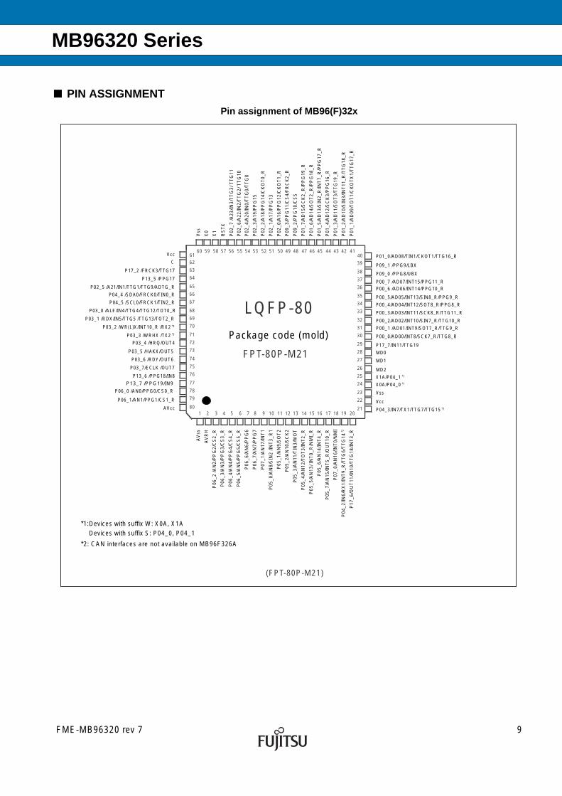
PIN ASSIGNMENTPin assignment of MB96(F)32x
60 59 58 57 56 55 54 53 52 51 50 49 48 47 46 45 44 43 42 41
78
77
76
75
74
73
72
71
70
69
68
67
66
65
64
63
62
23
24
25
26
27
28
29
30
31
32
33
34
35
36
37
38
39
8 9 10 11 12 13 14 15 16 17 18 19 201 2 3 4 5 76
79
8022
21
LQFP-80
61 40 P01_0/AD08/TIN1/CKOT1/TTG16_R
P09_1 /PPG9/LBX
P09_0 /PPG8/UBX
P00_7 /AD07/INT15/PPG11_RP00_6 /AD06/INT14/PPG10_R
P00_5/AD05/INT13/SIN8_R/PPG9_R
P00_4/AD04/INT12/SOT8_R/PPG8_R
P00_3/AD03/INT11/SCK8_R/TTG11_R
P00_2/AD02/INT10/SIN7_R/TTG10_R
P00_1 /AD01/INT9/SOT7_R/TTG9_R
P00_0/AD00/INT8/SCK7_R/TTG8_R
P17_7/IN11/TTG19
MD0
MD1
MD2
X1A/P04_1 *1
X0A/P04_0 *1
Vss
Vcc
P04_3/IN7/TX1/TTG7/TTG15 *2
P17_2 /FRCK3/TTG17
P13_5 /PPG17
P02_5 /A21/IN1/TTG1/TTG9/ADTG_R
P04_4 /SDA0/FRCK0/TIN0_R
P04_5 /SCL0/FRCK1/TIN2_R
P03_0 /ALE/IN4/TTG4/TTG12/TOT0_R
P03_1 /RDX/IN5/TTG5 /TTG13/TOT2_R
P03_2 /WR(L)X/INT10_R /RX2 *2
P03_3 /WRHX /TX2 *2
P03_4 /HRQ/OUT4
P03_5 /HAKX/OUT5
P03_6 /RDY/OUT6
P03_7/ECLK /OUT7
P13_6 /PPG18/IN8
P13_7 /PPG19/IN9
P06_0 /AN0/PPG0/CS0_R
P06_1/AN1/PPG1/CS1_R
AVcc
Vss
X0
X1
P02
_7 /A
23/IN
3/T
TG
3/ T
TG
11
P02
_6/A
22/IN
2/T
TG
2/ T
TG
10
RS
TX
P02
_4/A
20/IN
0/T
TG
0/T
TG
8
P02
_3/A
19/P
PG
15
P02
_2/A
18/P
PG
14/C
KO
T0_
R
P02
_1/A
17/P
PG
13
P02
_0/A
16/P
PG
12/C
KO
T1_
R
P09
_3/P
PG
11/C
S4/
FR
CK
2_R
P09
_2/P
PG
10/C
S5
P01
_7/A
D15
/SC
K2_
R/P
PG
19_R
P01
_6/A
D14
/SO
T2_
R/P
PG
18_R
P01
_5/A
D13
/SIN
2_R
/INT
7_R
/PP
G17
_R
P01
_4/A
D12
/SC
K3/
PP
G16
_R
P01
_3/A
D11
/SO
T3/
TT
G19
_R
P01
_2/A
D10
/SIN
3/IN
T11
_R/T
TG
18_R
P01
_1/A
D09
/TO
T1/
CK
OT
X1/
TT
G17
_R
AV
ss
AV
RH
P06
_2 /A
N2/
PP
G2/
CS
2_R
P06
_3/A
N3/
PP
G3/
CS
3_R
P06
_4/A
N4/
PP
G4/
CS
4_R
P06
_5/A
N5/
PP
G5/
CS
5_R
P06
_6/A
N6/
PP
G6
P06
_7/A
N7/
PP
G7
P07
_1/A
N17
/INT
1
P05
_0/A
N8/
SIN
2 /IN
T3_
R1
P05
_1/A
N9/
SO
T2
P05
_2/A
N10
/SC
K2
P05
_3/A
N11
/TIN
3/W
OT
P05
_4/A
N12
/TO
T3/
INT
2_R
P05
_5/A
N13
/ IN
T0_
R/N
MI_
R
P05
_6/A
N14
/INT
4_R
P05
_7/A
N15
/INT
5_R
/OU
T10
_R
P07
_0/A
N16
/INT
0/N
MI
P04
_2/IN
6/R
X1/
INT
9_R
/TT
G6/
TT
G14
*2
P17
_6/O
UT
11/IN
10/T
TG
18/IN
T3_
R
Package code (mold)
FPT-80P-M21
(FPT-80P-M21)
Devices with suffix W: X0A, X1A Devices with suffix S: P04_0, P04_1
*1:
Vcc
C
*2: CAN interfaces are not available on MB96F326A
MB96320 Series
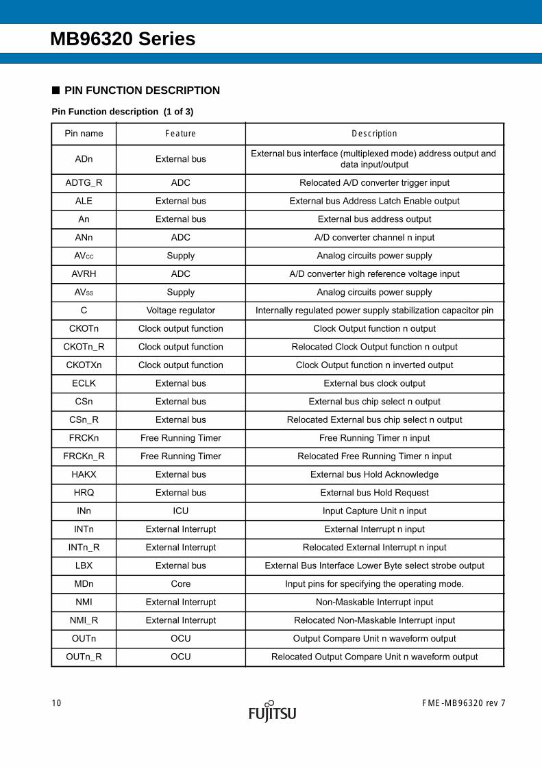
PIN FUNCTION DESCRIPTION
Pin Function description (1 of 3)
Pin name Feature Description
ADn External busExternal bus interface (multiplexed mode) address output and
data input/output
ADTG_R ADC Relocated A/D converter trigger input
ALE External bus External bus Address Latch Enable output
An External bus External bus address output
ANn ADC A/D converter channel n input
AVCC Supply Analog circuits power supply
AVRH ADC A/D converter high reference voltage input
AVSS Supply Analog circuits power supply
C Voltage regulator Internally regulated power supply stabilization capacitor pin
CKOTn Clock output function Clock Output function n output
CKOTn_R Clock output function Relocated Clock Output function n output
CKOTXn Clock output function Clock Output function n inverted output
ECLK External bus External bus clock output
CSn External bus External bus chip select n output
CSn_R External bus Relocated External bus chip select n output
FRCKn Free Running Timer Free Running Timer n input
FRCKn_R Free Running Timer Relocated Free Running Timer n input
HAKX External bus External bus Hold Acknowledge
HRQ External bus External bus Hold Request
INn ICU Input Capture Unit n input
INTn External Interrupt External Interrupt n input
INTn_R External Interrupt Relocated External Interrupt n input
LBX External bus External Bus Interface Lower Byte select strobe output
MDn Core Input pins for specifying the operating mode.
NMI External Interrupt Non-Maskable Interrupt input
NMI_R External Interrupt Relocated Non-Maskable Interrupt input
OUTn OCU Output Compare Unit n waveform output
OUTn_R OCU Relocated Output Compare Unit n waveform output
10 FME-MB96320 rev 7
MB96320 Series
Pxx_n GPIO General purpose IO
PPGn PPG Programmable Pulse Generator n output
PPGn_R PPG Relocated Programmable Pulse Generator n output
RDX External bus External bus interface read strobe output
RDY External bus External bus interface external wait state request input
RSTX Core Reset input
RXn CAN CAN interface n RX input
SCKn USART USART n serial clock input/output
SCKn_R USART Relocated USART n serial clock input/output
SCLn I2C I2C interface n clock I/O input/output
SDAn I2C I2C interface n serial data I/O input/output
SINn USART USART n serial data input
SINn_R USART Relocated USART n serial data input
SOTn USART USART n serial data output
SOTn_R USART Relocated USART n serial data output
TINn Reload Timer Reload Timer n event input
TINn_R Reload Timer Relocated Reload Timer n event input
TOTn Reload Timer Reload Timer n output
TOTn_R Reload Timer Relocated Reload Timer n output
TTGn PPG Programmable Pulse Generator n trigger input
TTGn_R PPG Relocated Programmable Pulse Generator n trigger input
TXn CAN CAN interface n TX output
UBX External bus External Bus Interface Upper Byte select strobe output
VCC Supply Power supply
VSS Supply Power supply
WOT RTC Real Timer clock output
WRHX External bus External bus High byte write strobe output
WRLX/WRX External bus External bus Low byte / Word write strobe output
X0 Clock Oscillator input
X0A Clock Subclock Oscillator input (only for devices with suffix "W")
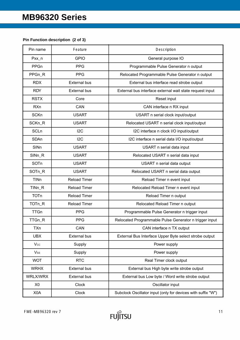
Pin Function description (2 of 3)
Pin name Feature Description
FME-MB96320 rev 7 11

MB96320 Series
X1 Clock Oscillator output
X1A Clock Subclock Oscillator output (only for devices with suffix "W")
Pin Function description (3 of 3)
Pin name Feature Description
12 FME-MB96320 rev 7

MB96320 Series
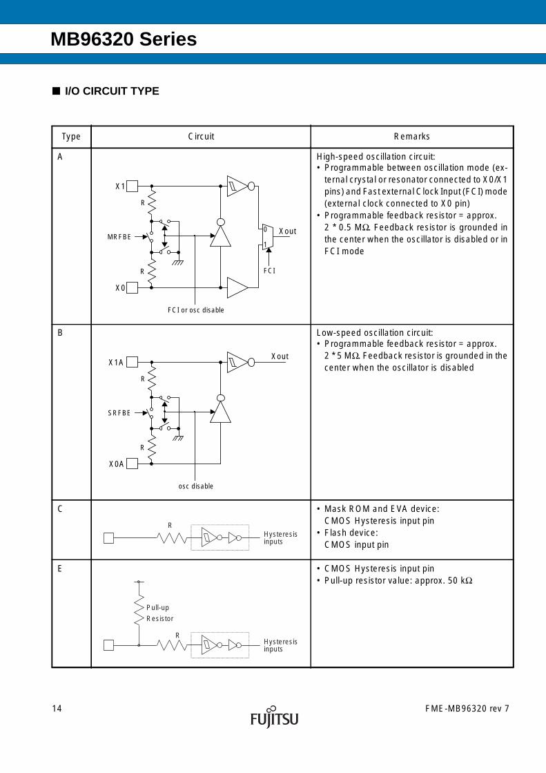
PIN CIRCUIT TYPE
*1: Please refer to “ I/O CIRCUIT TYPE” for details on the I/O circuit types*2: Devices with suffix ”W”*3: Devices without suffix ”W”
Pin circuit types
FPT-80P-M21
Pin no.Circuit type *1
1 Supply
2 G
3 to 18 I
19 to 21 H
22,23 Supply
24,25 B *2
24,25 H *3
26 to 28 C
29 to 56 H
57 E
58,59 A
60,61 Supply
62 F
63 to 65 H
66,67 N
68 to 77 H
78 to 79 I
80 Supply
FME-MB96320 rev 7 13
MB96320 Series
I/O CIRCUIT TYPE
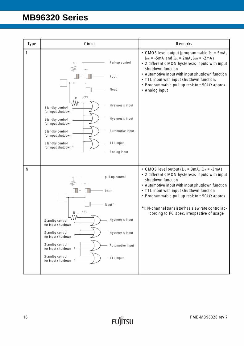
Type Circuit Remarks
A High-speed oscillation circuit:• Programmable between oscillation mode (ex-
ternal crystal or resonator connected to X0/X1pins) and Fast external Clock Input (FCI) mode(external clock connected to X0 pin)
• Programmable feedback resistor = approx.2 * 0.5 MΩ. Feedback resistor is grounded inthe center when the oscillator is disabled or inFCI mode
B Low-speed oscillation circuit:• Programmable feedback resistor = approx.
2 * 5 MΩ. Feedback resistor is grounded in thecenter when the oscillator is disabled
C • Mask ROM and EVA device:CMOS Hysteresis input pin
• Flash device:CMOS input pin
E • CMOS Hysteresis input pin• Pull-up resistor value: approx. 50 kΩ
X1
X0
R
R
MRFBEXout
FCI
0
1
FCI or osc disable
X1A
X0A
R
R
SRFBE
Xout
osc disable
RHysteresisinputs
R
Pull-up
Resistor
Hysteresisinputs
14 FME-MB96320 rev 7

MB96320 Series
F • Power supply input protection circuit
G • A/D converter ref+ (AVRH) power supply inputpin with protection circuit
• Flash devices do not have a protection circuitagainst VCC for pin AVRH
H • CMOS level output (programmable IOL = 5mA,IOH = -5mA and IOL = 2mA, IOH = -2mA)
• 2 different CMOS hysteresis inputs with inputshutdown function
• Automotive input with input shutdown function• TTL input with input shutdown function• Programmable pull-up resistor: 50kΩ approx.
Type Circuit Remarks
ANE
AVR
ANE
Pout
pull-up control
Nout
R
Hysteresis input
Automotive input
TTL input
Hysteresis input
Standby controlfor input shutdown
Standby controlfor input shutdown
Standby controlfor input shutdown
Standby controlfor input shutdown
FME-MB96320 rev 7 15
MB96320 Series
I • CMOS level output (programmable IOL = 5mA,IOH = -5mA and IOL = 2mA, IOH = -2mA)
• 2 different CMOS hysteresis inputs with inputshutdown function
• Automotive input with input shutdown function• TTL input with input shutdown function.• Programmable pull-up resistor: 50kΩ approx.• Analog input
N • CMOS level output (IOL = 3mA, IOH = -3mA)• 2 different CMOS hysteresis inputs with input
shutdown function• Automotive input with input shutdown function• TTL input with input shutdown function• Programmable pull-up resistor: 50kΩ approx.
*1: N-channel transistor has slew rate control ac-cording to I2C spec, irrespective of usage
Type Circuit Remarks
R
Hysteresis input
Hysteresis input
Standby controlfor input shutdown
Standby controlfor input shutdown
Standby controlfor input shutdown
Standby controlfor input shutdown
Pull-up control
Pout
Nout
Automotive input
TTL input
Analog input
Pout
pull-up control
Nout *1
R
Hysteresis input
Automotive input
TTL input
Hysteresis input
Standby controlfor input shutdown
Standby controlfor input shutdown
Standby controlfor input shutdown
Standby controlfor input shutdown
16 FME-MB96320 rev 7

MB96320 Series
MEMORY MAP
MB96V300B MB96(F)32x
FF:FFFFH
Emulation ROMUSER ROM /
External Bus*4
DE:0000H
External Bus External Bus
10:0000H
0F:E000H
Boot-ROM Boot-ROM
Reserved
Reserved0E:0000H
External RAM
02:0000H
Internal RAM
bank 1
ReservedRAMEND1*2 Internal RAM
bank 1RAM availability de-pending on the deviceRAMSTART12
01:0000H Reserved
ROM/RAM MIRROR ROM/RAM MIRROR00:8000H
Internal RAM
bank 0
Internal RAM
bank 0RAMSTART0*2
Reserved
RAMSTART0*3 External Bus
External Bus endaddress*2
00:0C00HExternal Bus
Peripherals Peripherals00:0380H
00:0180HGPR*1 GPR*1
00:0100HDMA DMA
00:00F0HExternal Bus External Bus
00:0000HPeripheral Peripheral
*1: Unused GPR banks can be used as RAM area
*2: For External Bus end address and RAMSTART/END addresses, please refer to the table on the next page.
*3: For EVA device, RAMSTART0 depends on the configuration of the emulated device.
*4: For details about USER ROM area, see the USER ROM MEMORY MAP FOR FLASH DEVICES on thefollowing pages.
The External Bus area and DMA area are only available if the device contains the corresponding resource.
The available RAM and ROM area depends on the device.
FME-MB96320 rev 7 17

MB96320 Series
RAMSTART/END AND EXTERNAL BUS END ADDRESSES
USER ROM MEMORY MAP FOR FLASH DEVICES
Devices Bank 0RAM size
Bank 1RAM size
External Busend address RAMSTART0 RAMSTART1 RAMEND1
MB96F326 12KByte - 00:51FFH 00:5240H - -
MB96F326
Alternative modeCPU address
Flash memorymode address
Flash size288kByte
FF:FFFFH
FF:0000H
3F:FFFFH
3F:0000HS39 - 64K
Flash AFE:FFFFH
FE:0000H
3E:FFFFH
3E:0000HS38 - 64K
FD:FFFFH
FD:0000H
3D:FFFFH
3D:0000HS37 - 64K
FC:FFFFH
FC:0000H
3C:FFFFH
3C:0000HS36 - 64K
FB:FFFFH
FB:0000H
3B:FFFFH
3B:0000H
External bus
FA:FFFFH
FA:0000H
3A:FFFFH
3A:0000H
F9:FFFFH
F9:0000H
39:FFFFH
39:0000H
F8:FFFFH
F8:0000H
38:FFFFH
38:0000H
F7:FFFFH
F7:0000H
37:FFFFH
37:0000H
F6:FFFFH
F6:0000H
36:FFFFH
36:0000H
F5:FFFFH
F5:0000H
35:FFFFH
35:0000H
F4:FFFFH
F4:0000H
34:FFFFH
34:0000H
F3:FFFFH
F3:0000H
33:FFFFH
33:0000H
F2:FFFFH
F2:0000H
32:FFFFH
32:0000H
F1:FFFFH
F1:0000H
31:FFFFH
31:0000H
F0:FFFFH
F0:0000H
30:FFFFH
30:0000H
E0:FFFFH
E0:0000H
DF:FFFFH
DF:8000H
ReservedDF:7FFFH
DF:6000H
1F:7FFFH
1F:6000HSA3 - 8K
Flash ADF:5FFFH
DF:4000H
1F:5FFFH
1F:4000HSA2 - 8K
DF:3FFFH
DF:2000H
1F:3FFFH
1F:2000HSA1 - 8K
DF:1FFFH
DF:0000H
1F:1FFFH
1F:0000HSA0 - 8K *1
DE:FFFFH
DE:0000H
Reserved
*1: Sector SA0 contains the ROM Configuration Block RCBA at CPU address DF:0000H - DF:007FH
18 FME-MB96320 rev 7
MB96320 Series
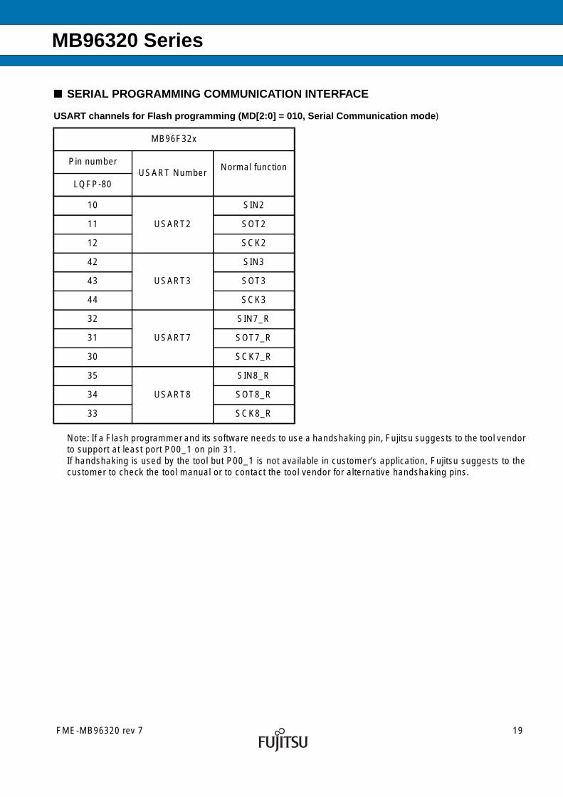
SERIAL PROGRAMMING COMMUNICATION INTERFACE
Note: If a Flash programmer and its software needs to use a handshaking pin, Fujitsu suggests to the tool vendorto support at least port P00_1 on pin 31.If handshaking is used by the tool but P00_1 is not available in customer’s application, Fujitsu suggests to thecustomer to check the tool manual or to contact the tool vendor for alternative handshaking pins.
USART channels for Flash programming (MD[2:0] = 010, Serial Communication mode)
MB96F32x
Pin numberUSART Number
Normal function
LQFP-80
10
USART2
SIN2
11 SOT2
12 SCK2
42
USART3
SIN3
43 SOT3
44 SCK3
32
USART7
SIN7_R
31 SOT7_R
30 SCK7_R
35
USART8
SIN8_R
34 SOT8_R
33 SCK8_R
FME-MB96320 rev 7 19

MB96320 Series
I/O MAP
I/O map MB96(F)32x (1 of 31)
Address Register Abbreviation8-bit access
Abbreviation16-bit access Access
000000H I/O Port P00 - Port Data Register PDR00 R/W
000001H I/O Port P01 - Port Data Register PDR01 R/W
000002H I/O Port P02 - Port Data Register PDR02 R/W
000003H I/O Port P03 - Port Data Register PDR03 R/W
000004H I/O Port P04 - Port Data Register PDR04 R/W
000005H I/O Port P05 - Port Data Register PDR05 R/W
000006H I/O Port P06 - Port Data Register PDR06 R/W
000007H I/O Port P07 - Port Data Register PDR07 R/W
000008H Reserved -
000009H I/O Port P09 - Port Data Register PDR09 R/W
00000AH-00000CH
Reserved -
00000DH I/O Port P13 - Port Data Register PDR13 R/W
00000EH-000010H
Reserved -
000011H I/O Port P17 - Port Data Register PDR17 R/W
000012H-000017H
Reserved -
000018H ADC0 - Control Status register Low ADCSL ADCS R/W
000019H ADC0 - Control Status register High ADCSH R/W
00001AH ADC0 - Data Register Low ADCRL ADCR R
00001BH ADC0 - Data Register High ADCRH R
00001CH ADC0 - Setting Register ADSR R/W
00001DH ADC0 - Setting Register R/W
00001EH ADC0 - Extended Configuration Register ADECR R/W
00001FH Reserved -
000020H FRT0 - Data register of free-running timer TCDT0 R/W
000021H FRT0 - Data register of free-running timer R/W
000022HFRT0 - Control status register of free-running timerLow
TCCSL0 TCCS0 R/W
20 FME-MB96320 rev 7
MB96320 Series
000023HFRT0 - Control status register of free-running timerHigh
TCCSH0 R/W
000024H FRT1 - Data register of free-running timer TCDT1 R/W
000025H FRT1 - Data register of free-running timer R/W
000026HFRT1 - Control status register of free-running timerLow
TCCSL1 TCCS1 R/W
000027HFRT1 - Control status register of free-running timerHigh
TCCSH1 R/W
000028H-000033H
Reserved -
000034H OCU4 - Output Compare Control Status OCS4 R/W
000035H OCU5 - Output Compare Control Status OCS5 R/W
000036H OCU4 - Compare Register OCCP4 R/W
000037H OCU4 - Compare Register R/W
000038H OCU5 - Compare Register OCCP5 R/W
000039H OCU5 - Compare Register R/W
00003AH OCU6 - Output Compare Control Status OCS6 R/W
00003BH OCU7 - Output Compare Control Status OCS7 R/W
00003CH OCU6 - Compare Register OCCP6 R/W
00003DH OCU6 - Compare Register R/W
00003EH OCU7 - Compare Register OCCP7 R/W
00003FH OCU7 - Compare Register R/W
000040H ICU0/ICU1 - Control Status Register ICS01 R/W
000041H ICU0/ICU1 - Edge register ICE01 R/W
000042H ICU0 - Capture Register Low IPCPL0 IPCP0 R
000043H ICU0 - Capture Register High IPCPH0 R
000044H ICU1 - Capture Register Low IPCPL1 IPCP1 R
000045H ICU1 - Capture Register High IPCPH1 R
000046H ICU2/ICU3 - Control Status Register ICS23 R/W
000047H ICU2/ICU3 - Edge register ICE23 R/W
000048H ICU2 - Capture Register Low IPCPL2 IPCP2 R
I/O map MB96(F)32x (2 of 31)
Address Register Abbreviation8-bit access
Abbreviation16-bit access Access
FME-MB96320 rev 7 21

MB96320 Series
000049H ICU2 - Capture Register High IPCPH2 R
00004AH ICU3 - Capture Register Low IPCPL3 IPCP3 R
00004BH ICU3 - Capture Register High IPCPH3 R
00004CH ICU4/ICU5 - Control Status Register ICS45 R/W
00004DH ICU4/ICU5 - Edge register ICE45 R/W
00004EH ICU4 - Capture Register Low IPCPL4 IPCP4 R
00004FH ICU4 - Capture Register High IPCPH4 R
000050H ICU5 - Capture Register Low IPCPL5 IPCP5 R
000051H ICU5 - Capture Register High IPCPH5 R
000052H ICU6/ICU7 - Control Status Register ICS67 R/W
000053H ICU6/ICU7 - Edge register ICE67 R/W
000054H ICU6 - Capture Register Low IPCPL6 IPCP6 R
000055H ICU6 - Capture Register High IPCPH6 R
000056H ICU7 - Capture Register Low IPCPL7 IPCP7 R
000057H ICU7 - Capture Register High IPCPH7 R
000058H EXTINT0 - External Interrupt Enable Register ENIR0 R/W
000059HEXTINT0 - External Interrupt Interrupt request Reg-ister
EIRR0 R/W
00005AH EXTINT0 - External Interrupt Level Select Low ELVRL0 ELVR0 R/W
00005BH EXTINT0 - External Interrupt Level Select High ELVRH0 R/W
00005CH EXTINT1 - External Interrupt Enable Register ENIR1 R/W
00005DHEXTINT1 - External Interrupt Interrupt request Reg-ister
EIRR1 R/W
00005EH EXTINT1 - External Interrupt Level Select Low ELVRL1 ELVR1 R/W
00005FH EXTINT1 - External Interrupt Level Select High ELVRH1 R/W
000060H RLT0 - Timer Control Status Register Low TMCSRL0 TMCSR0 R/W
000061H RLT0 - Timer Control Status Register High TMCSRH0 R/W
000062H RLT0 - Reload Register - for writing TMRLR0 W
000062H RLT0 - Reload Register - for reading TMR0 R
000063H RLT0 - Reload Register - for writing W
000063H RLT0 - Reload Register - for reading R
I/O map MB96(F)32x (3 of 31)
Address Register Abbreviation8-bit access
Abbreviation16-bit access Access
22 FME-MB96320 rev 7

MB96320 Series
000064H RLT1 - Timer Control Status Register Low TMCSRL1 TMCSR1 R/W
000065H RLT1 - Timer Control Status Register High TMCSRH1 R/W
000066H RLT1 - Reload Register - for writing TMRLR1 W
000066H RLT1 - Reload Register - for reading TMR1 R
000067H RLT1 - Reload Register - for writing W
000067H RLT1 - Reload Register - for reading R
000068H RLT2 - Timer Control Status Register Low TMCSRL2 TMCSR2 R/W
000069H RLT2 - Timer Control Status Register High TMCSRH2 R/W
00006AH RLT2 - Reload Register - for writing TMRLR2 W
00006AH RLT2 - Reload Register - for reading TMR2 R
00006BH RLT2 - Reload Register - for writing W
00006BH RLT2 - Reload Register - for reading R
00006CH RLT3 - Timer Control Status Register Low TMCSRL3 TMCSR3 R/W
00006DH RLT3 - Timer Control Status Register High TMCSRH3 R/W
00006EH RLT3 - Reload Register - for writing TMRLR3 W
00006EH RLT3 - Reload Register - for reading TMR3 R
00006FH RLT3 - Reload Register - for writing W
00006FH RLT3 - Reload Register - for reading R
000070HRLT6 - Timer Control Status Register Low (dedic.RLT for PPG)
TMCSRL6 TMCSR6 R/W
000071HRLT6 - Timer Control Status Register High (dedic.RLT for PPG)
TMCSRH6 R/W
000072HRLT6 - Reload Register (dedic. RLT for PPG) - forwriting
TMRLR6 W
000072HRLT6 - Reload Register (dedic. RLT for PPG) - forreading
TMR6 R
000073HRLT6 - Reload Register (dedic. RLT for PPG) - forwriting
W
000073HRLT6 - Reload Register (dedic. RLT for PPG) - forreading
R
000074H PPG3-PPG0 - General Control register 1 Low GCN1L0 GCN10 R/W
000075H PPG3-PPG0 - General Control register 1 High GCN1H0 R/W
I/O map MB96(F)32x (4 of 31)
Address Register Abbreviation8-bit access
Abbreviation16-bit access Access
FME-MB96320 rev 7 23

MB96320 Series
000076H PPG3-PPG0 - General Control register 2 Low GCN2L0 GCN20 R/W
000077H PPG3-PPG0 - General Control register 2 High GCN2H0 R/W
000078H PPG0 - Timer register PTMR0 R
000079H PPG0 - Timer register R
00007AH PPG0 - Period setting register PCSR0 W
00007BH PPG0 - Period setting register W
00007CH PPG0 - Duty cycle register PDUT0 W
00007DH PPG0 - Duty cycle register W
00007EH PPG0 - Control status register Low PCNL0 PCN0 R/W
00007FH PPG0 - Control status register High PCNH0 R/W
000080H PPG1 - Timer register PTMR1 R
000081H PPG1 - Timer register R
000082H PPG1 - Period setting register PCSR1 W
000083H PPG1 - Period setting register W
000084H PPG1 - Duty cycle register PDUT1 W
000085H PPG1 - Duty cycle register W
000086H PPG1 - Control status register Low PCNL1 PCN1 R/W
000087H PPG1 - Control status register High PCNH1 R/W
000088H PPG2 - Timer register PTMR2 R
000089H PPG2 - Timer register R
00008AH PPG2 - Period setting register PCSR2 W
00008BH PPG2 - Period setting register W
00008CH PPG2 - Duty cycle register PDUT2 W
00008DH PPG2 - Duty cycle register W
00008EH PPG2 - Control status register Low PCNL2 PCN2 R/W
00008FH PPG2 - Control status register High PCNH2 R/W
000090H PPG3 - Timer register PTMR3 R
000091H PPG3 - Timer register R
000092H PPG3 - Period setting register PCSR3 W
000093H PPG3 - Period setting register W
I/O map MB96(F)32x (5 of 31)
Address Register Abbreviation8-bit access
Abbreviation16-bit access Access
24 FME-MB96320 rev 7

MB96320 Series
000094H PPG3 - Duty cycle register PDUT3 W
000095H PPG3 - Duty cycle register W
000096H PPG3 - Control status register Low PCNL3 PCN3 R/W
000097H PPG3 - Control status register High PCNH3 R/W
000098H PPG7-PPG4 - General Control register 1 Low GCN1L1 GCN11 R/W
000099H PPG7-PPG4 - General Control register 1 High GCN1H1 R/W
00009AH PPG7-PPG4 - General Control register 2 Low GCN2L1 GCN21 R/W
00009BH PPG7-PPG4 - General Control register 2 High GCN2H1 R/W
00009CH PPG4 - Timer register PTMR4 R
00009DH PPG4 - Timer register R
00009EH PPG4 - Period setting register PCSR4 W
00009FH PPG4 - Period setting register W
0000A0H PPG4 - Duty cycle register PDUT4 W
0000A1H PPG4 - Duty cycle register W
0000A2H PPG4 - Control status register Low PCNL4 PCN4 R/W
0000A3H PPG4 - Control status register High PCNH4 R/W
0000A4H PPG5 - Timer register PTMR5 R
0000A5H PPG5 - Timer register R
0000A6H PPG5 - Period setting register PCSR5 W
0000A7H PPG5 - Period setting register W
0000A8H PPG5 - Duty cycle register PDUT5 W
0000A9H PPG5 - Duty cycle register W
0000AAH PPG5 - Control status register Low PCNL5 PCN5 R/W
0000ABH PPG5 - Control status register High PCNH5 R/W
0000ACH I2C0 - Bus Status Register IBSR0 R
0000ADH I2C0 - Bus Control Register IBCR0 R/W
0000AEH I2C0 - Ten bit Slave address Register Low ITBAL0 ITBA0 R/W
0000AFH I2C0 - Ten bit Slave address Register High ITBAH0 R/W
0000B0H I2C0 - Ten bit Address mask Register Low ITMKL0 ITMK0 R/W
0000B1H I2C0 - Ten bit Address mask Register High ITMKH0 R/W
I/O map MB96(F)32x (6 of 31)
Address Register Abbreviation8-bit access
Abbreviation16-bit access Access
FME-MB96320 rev 7 25

MB96320 Series
0000B2H I2C0 - Seven bit Slave address Register ISBA0 R/W
0000B3H I2C0 - Seven bit Address mask Register ISMK0 R/W
0000B4H I2C0 - Data Register IDAR0 R/W
0000B5H I2C0 - Clock Control Register ICCR0 R/W
0000B6H-0000D3H
Reserved -
0000D4H USART2 - Serial Mode Register SMR2 R/W
0000D5H USART2 - Serial Control Register SCR2 R/W
0000D6H USART2 - TX Register TDR2 W
0000D6H USART2 - RX Register RDR2 R
0000D7H USART2 - Serial Status SSR2 R/W
0000D8H USART2 - Control/Com. Register ECCR2 R/W
0000D9H USART2 - Ext. Status Register ESCR2 R/W
0000DAH USART2 - Baud Rate Generator Register Low BGRL2 BGR2 R/W
0000DBH USART2 - Baud Rate Generator Register High BGRH2 R/W
0000DCH USART2 - Extended Serial Interrupt Register ESIR2 R/W
0000DDH Reserved -
0000DEH USART3 - Serial Mode Register SMR3 R/W
0000DFH USART3 - Serial Control Register SCR3 R/W
0000E0H USART3 - TX Register TDR3 W
0000E0H USART3 - RX Register RDR3 R
0000E1H USART3 - Serial Status SSR3 R/W
0000E2H USART3 - Control/Com. Register ECCR3 R/W
0000E3H USART3 - Ext. Status Register ESCR3 R/W
0000E4H USART3 - Baud Rate Generator Register Low BGRL3 BGR3 R/W
0000E5H USART3 - Baud Rate Generator Register High BGRH3 R/W
0000E6H USART3 - Extended Serial Interrupt Register ESIR3 R/W
0000E7H-0000EFH
Reserved -
0000F0H-0000FFH
External Bus area EXTBUS0 R/W
I/O map MB96(F)32x (7 of 31)
Address Register Abbreviation8-bit access
Abbreviation16-bit access Access
26 FME-MB96320 rev 7

MB96320 Series
000100H DMA0 - Buffer address pointer low byte BAPL0 R/W
000101H DMA0 - Buffer address pointer middle byte BAPM0 R/W
000102H DMA0 - Buffer address pointer high byte BAPH0 R/W
000103H DMA0 - DMA control register DMACS0 R/W
000104H DMA0 - I/O register address pointer low byte IOAL0 IOA0 R/W
000105H DMA0 - I/O register address pointer high byte IOAH0 R/W
000106H DMA0 - Data counter low byte DCTL0 DCT0 R/W
000107H DMA0 - Data counter high byte DCTH0 R/W
000108H DMA1 - Buffer address pointer low byte BAPL1 R/W
000109H DMA1 - Buffer address pointer middle byte BAPM1 R/W
00010AH DMA1 - Buffer address pointer high byte BAPH1 R/W
00010BH DMA1 - DMA control register DMACS1 R/W
00010CH DMA1 - I/O register address pointer low byte IOAL1 IOA1 R/W
00010DH DMA1 - I/O register address pointer high byte IOAH1 R/W
00010EH DMA1 - Data counter low byte DCTL1 DCT1 R/W
00010FH DMA1 - Data counter high byte DCTH1 R/W
000110H DMA2 - Buffer address pointer low byte BAPL2 R/W
000111H DMA2 - Buffer address pointer middle byte BAPM2 R/W
000112H DMA2 - Buffer address pointer high byte BAPH2 R/W
000113H DMA2 - DMA control register DMACS2 R/W
000114H DMA2 - I/O register address pointer low byte IOAL2 IOA2 R/W
000115H DMA2 - I/O register address pointer high byte IOAH2 R/W
000116H DMA2 - Data counter low byte DCTL2 DCT2 R/W
000117H DMA2 - Data counter high byte DCTH2 R/W
000118H DMA3 - Buffer address pointer low byte BAPL3 R/W
000119H DMA3 - Buffer address pointer middle byte BAPM3 R/W
00011AH DMA3 - Buffer address pointer high byte BAPH3 R/W
00011BH DMA3 - DMA control register DMACS3 R/W
00011CH DMA3 - I/O register address pointer low byte IOAL3 IOA3 R/W
00011DH DMA3 - I/O register address pointer high byte IOAH3 R/W
I/O map MB96(F)32x (8 of 31)
Address Register Abbreviation8-bit access
Abbreviation16-bit access Access
FME-MB96320 rev 7 27
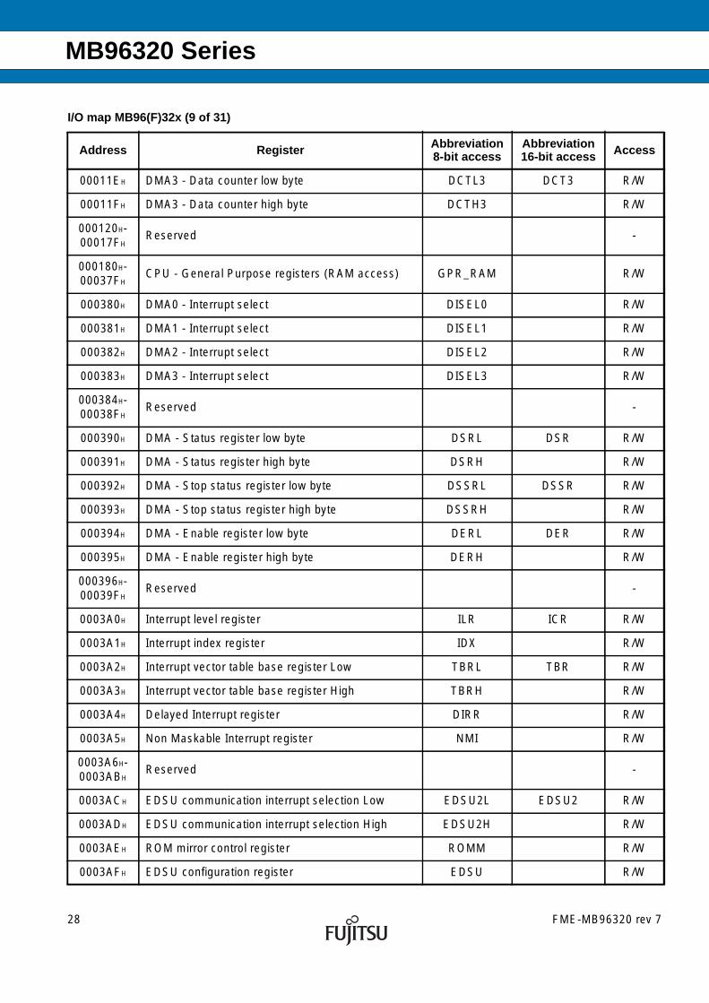
MB96320 Series
00011EH DMA3 - Data counter low byte DCTL3 DCT3 R/W
00011FH DMA3 - Data counter high byte DCTH3 R/W
000120H-00017FH
Reserved -
000180H-00037FH
CPU - General Purpose registers (RAM access) GPR_RAM R/W
000380H DMA0 - Interrupt select DISEL0 R/W
000381H DMA1 - Interrupt select DISEL1 R/W
000382H DMA2 - Interrupt select DISEL2 R/W
000383H DMA3 - Interrupt select DISEL3 R/W
000384H-00038FH
Reserved -
000390H DMA - Status register low byte DSRL DSR R/W
000391H DMA - Status register high byte DSRH R/W
000392H DMA - Stop status register low byte DSSRL DSSR R/W
000393H DMA - Stop status register high byte DSSRH R/W
000394H DMA - Enable register low byte DERL DER R/W
000395H DMA - Enable register high byte DERH R/W
000396H-00039FH
Reserved -
0003A0H Interrupt level register ILR ICR R/W
0003A1H Interrupt index register IDX R/W
0003A2H Interrupt vector table base register Low TBRL TBR R/W
0003A3H Interrupt vector table base register High TBRH R/W
0003A4H Delayed Interrupt register DIRR R/W
0003A5H Non Maskable Interrupt register NMI R/W
0003A6H-0003ABH
Reserved -
0003ACH EDSU communication interrupt selection Low EDSU2L EDSU2 R/W
0003ADH EDSU communication interrupt selection High EDSU2H R/W
0003AEH ROM mirror control register ROMM R/W
0003AFH EDSU configuration register EDSU R/W
I/O map MB96(F)32x (9 of 31)
Address Register Abbreviation8-bit access
Abbreviation16-bit access Access
28 FME-MB96320 rev 7
MB96320 Series
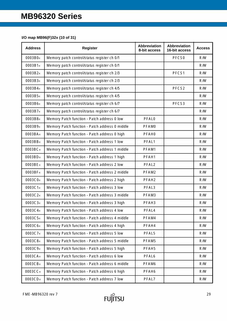
0003B0H Memory patch control/status register ch 0/1 PFCS0 R/W
0003B1H Memory patch control/status register ch 0/1 R/W
0003B2H Memory patch control/status register ch 2/3 PFCS1 R/W
0003B3H Memory patch control/status register ch 2/3 R/W
0003B4H Memory patch control/status register ch 4/5 PFCS2 R/W
0003B5H Memory patch control/status register ch 4/5 R/W
0003B6H Memory patch control/status register ch 6/7 PFCS3 R/W
0003B7H Memory patch control/status register ch 6/7 R/W
0003B8H Memory Patch function - Patch address 0 low PFAL0 R/W
0003B9H Memory Patch function - Patch address 0 middle PFAM0 R/W
0003BAH Memory Patch function - Patch address 0 high PFAH0 R/W
0003BBH Memory Patch function - Patch address 1 low PFAL1 R/W
0003BCH Memory Patch function - Patch address 1 middle PFAM1 R/W
0003BDH Memory Patch function - Patch address 1 high PFAH1 R/W
0003BEH Memory Patch function - Patch address 2 low PFAL2 R/W
0003BFH Memory Patch function - Patch address 2 middle PFAM2 R/W
0003C0H Memory Patch function - Patch address 2 high PFAH2 R/W
0003C1H Memory Patch function - Patch address 3 low PFAL3 R/W
0003C2H Memory Patch function - Patch address 3 middle PFAM3 R/W
0003C3H Memory Patch function - Patch address 3 high PFAH3 R/W
0003C4H Memory Patch function - Patch address 4 low PFAL4 R/W
0003C5H Memory Patch function - Patch address 4 middle PFAM4 R/W
0003C6H Memory Patch function - Patch address 4 high PFAH4 R/W
0003C7H Memory Patch function - Patch address 5 low PFAL5 R/W
0003C8H Memory Patch function - Patch address 5 middle PFAM5 R/W
0003C9H Memory Patch function - Patch address 5 high PFAH5 R/W
0003CAH Memory Patch function - Patch address 6 low PFAL6 R/W
0003CBH Memory Patch function - Patch address 6 middle PFAM6 R/W
0003CCH Memory Patch function - Patch address 6 high PFAH6 R/W
0003CDH Memory Patch function - Patch address 7 low PFAL7 R/W
I/O map MB96(F)32x (10 of 31)
Address Register Abbreviation8-bit access
Abbreviation16-bit access Access
FME-MB96320 rev 7 29

MB96320 Series
0003CEH Memory Patch function - Patch address 7 middle PFAM7 R/W
0003CFH Memory Patch function - Patch address 7 high PFAH7 R/W
0003D0H Memory Patch function - Patch data 0 Low PFDL0 PFD0 R/W
0003D1H Memory Patch function - Patch data 0 High PFDH0 R/W
0003D2H Memory Patch function - Patch data 1 Low PFDL1 PFD1 R/W
0003D3H Memory Patch function - Patch data 1 High PFDH1 R/W
0003D4H Memory Patch function - Patch data 2 Low PFDL2 PFD2 R/W
0003D5H Memory Patch function - Patch data 2 High PFDH2 R/W
0003D6H Memory Patch function - Patch data 3 Low PFDL3 PFD3 R/W
0003D7H Memory Patch function - Patch data 3 High PFDH3 R/W
0003D8H Memory Patch function - Patch data 4 Low PFDL4 PFD4 R/W
0003D9H Memory Patch function - Patch data 4 High PFDH4 R/W
0003DAH Memory Patch function - Patch data 5 Low PFDL5 PFD5 R/W
0003DBH Memory Patch function - Patch data 5 High PFDH5 R/W
0003DCH Memory Patch function - Patch data 6 Low PFDL6 PFD6 R/W
0003DDH Memory Patch function - Patch data 6 High PFDH6 R/W
0003DEH Memory Patch function - Patch data 7 Low PFDL7 PFD7 R/W
0003DFH Memory Patch function - Patch data 7 High PFDH7 R/W
0003E0H-0003F0H
Reserved -
0003F1H Memory Control Status Register A MCSRA R/W
0003F2H Memory Timing Configuration Register A Low MTCRAL MTCRA R/W
0003F3H Memory Timing Configuration Register A High MTCRAH R/W
0003F4H-0003F8H
Reserved -
0003F9H Flash Memory Write Control register 1 FMWC1 R/W
0003FAH Flash Memory Write Control register 2 FMWC2 R/W
0003FBH Flash Memory Write Control register 3 FMWC3 R/W
0003FCH Flash Memory Write Control register 4 FMWC4 R/W
0003FDH Flash Memory Write Control register 5 FMWC5 R/W
I/O map MB96(F)32x (11 of 31)
Address Register Abbreviation8-bit access
Abbreviation16-bit access Access
30 FME-MB96320 rev 7

MB96320 Series
0003FEH-0003FFH
Reserved -
000400H Standby Mode control register SMCR R/W
000401H Clock select register CKSR R/W
000402H Clock Stabilization select register CKSSR R/W
000403H Clock monitor register CKMR R
000404H Clock Frequency control register Low CKFCRL CKFCR R/W
000405H Clock Frequency control register High CKFCRH R/W
000406H PLL Control register Low PLLCRL PLLCR R/W
000407H PLL Control register High PLLCRH R/W
000408H RC clock timer control register RCTCR R/W
000409H Main clock timer control register MCTCR R/W
00040AH Sub clock timer control register SCTCR R/W
00040BHReset cause and clock status register with clearfunction
RCCSRC R
00040CH Reset configuration register RCR R/W
00040DH Reset cause and clock status register RCCSR R
00040EH Watch dog timer configuration register WDTC R/W
00040FH Watch dog timer clear pattern register WDTCP W
000410H-000414H
Reserved -
000415H Clock output activation register COAR R/W
000416H Clock output configuration register 0 COCR0 R/W
000417H Clock output configuration register 1 COCR1 R/W
000418H Clock Modulator control register CMCR R/W
000419H Reserved -
00041AH Clock Modulator Parameter register Low CMPRL CMPR R/W
00041BH Clock Modulator Parameter register High CMPRH R/W
00041CH-00042BH
Reserved -
00042CH Voltage Regulator Control register VRCR R/W
I/O map MB96(F)32x (12 of 31)
Address Register Abbreviation8-bit access
Abbreviation16-bit access Access
FME-MB96320 rev 7 31

MB96320 Series
00042DH Clock Input and LVD Control Register CILCR R/W
00042EH-00042FH
Reserved -
000430H I/O Port P00 - Data Direction Register DDR00 R/W
000431H I/O Port P01 - Data Direction Register DDR01 R/W
000432H I/O Port P02 - Data Direction Register DDR02 R/W
000433H I/O Port P03 - Data Direction Register DDR03 R/W
000434H I/O Port P04 - Data Direction Register DDR04 R/W
000435H I/O Port P05 - Data Direction Register DDR05 R/W
000436H I/O Port P06 - Data Direction Register DDR06 R/W
000437H I/O Port P07 - Data Direction Register DDR07 R/W
000438H Reserved -
000439H I/O Port P09 - Data Direction Register DDR09 R/W
00043AH-00043CH
Reserved -
00043DH I/O Port P13 - Data Direction Register DDR13 R/W
00043EH-000440H
Reserved -
000441H I/O Port P17 - Data Direction Register DDR17 R/W
000442H-000443H
Reserved -
000444H I/O Port P00 - Port Input Enable Register PIER00 R/W
000445H I/O Port P01 - Port Input Enable Register PIER01 R/W
000446H I/O Port P02 - Port Input Enable Register PIER02 R/W
000447H I/O Port P03 - Port Input Enable Register PIER03 R/W
000448H I/O Port P04 - Port Input Enable Register PIER04 R/W
000449H I/O Port P05 - Port Input Enable Register PIER05 R/W
00044AH I/O Port P06 - Port Input Enable Register PIER06 R/W
00044BH I/O Port P07 - Port Input Enable Register PIER07 R/W
00044CH Reserved -
00044DH I/O Port P09 - Port Input Enable Register PIER09 R/W
I/O map MB96(F)32x (13 of 31)
Address Register Abbreviation8-bit access
Abbreviation16-bit access Access
32 FME-MB96320 rev 7

MB96320 Series
00044EH-000450H
Reserved -
000451H I/O Port P13 - Port Input Enable Register PIER13 R/W
000452H-000454H
Reserved -
000455H I/O Port P17 - Port Input Enable Register PIER17 R/W
000456H-000457H
Reserved -
000458H I/O Port P00 - Port Input Level Register PILR00 R/W
000459H I/O Port P01 - Port Input Level Register PILR01 R/W
00045AH I/O Port P02 - Port Input Level Register PILR02 R/W
00045BH I/O Port P03 - Port Input Level Register PILR03 R/W
00045CH I/O Port P04 - Port Input Level Register PILR04 R/W
00045DH I/O Port P05 - Port Input Level Register PILR05 R/W
00045EH I/O Port P06 - Port Input Level Register PILR06 R/W
00045FH I/O Port P07 - Port Input Level Register PILR07 R/W
000460H Reserved -
000461H I/O Port P09 - Port Input Level Register PILR09 R/W
000462H-000464H
Reserved -
000465H I/O Port P13 - Port Input Level Register PILR13 R/W
000466H-000468H
Reserved -
000469H I/O Port P17 - Port Input Level Register PILR17 R/W
00046AH-00046BH
Reserved -
00046CH I/O Port P00 - Extended Port Input Level Register EPILR00 R/W
00046DH I/O Port P01 - Extended Port Input Level Register EPILR01 R/W
00046EH I/O Port P02 - Extended Port Input Level Register EPILR02 R/W
00046FH I/O Port P03 - Extended Port Input Level Register EPILR03 R/W
000470H I/O Port P04 - Extended Port Input Level Register EPILR04 R/W
000471H I/O Port P05 - Extended Port Input Level Register EPILR05 R/W
I/O map MB96(F)32x (14 of 31)
Address Register Abbreviation8-bit access
Abbreviation16-bit access Access
FME-MB96320 rev 7 33

MB96320 Series
000472H I/O Port P06 - Extended Port Input Level Register EPILR06 R/W
000473H I/O Port P07 - Extended Port Input Level Register EPILR07 R/W
000474H Reserved -
000475H I/O Port P09 - Extended Port Input Level Register EPILR09 R/W
000476H-000478H
Reserved -
000479H I/O Port P13 - Extended Port Input Level Register EPILR13 R/W
00047AH-00047CH
Reserved -
00047DH I/O Port P17 - Extended Port Input Level Register EPILR17 R/W
00047EH-00047FH
Reserved -
000480H I/O Port P00 - Port Output Drive Register PODR00 R/W
000481H I/O Port P01 - Port Output Drive Register PODR01 R/W
000482H I/O Port P02 - Port Output Drive Register PODR02 R/W
000483H I/O Port P03 - Port Output Drive Register PODR03 R/W
000484H I/O Port P04 - Port Output Drive Register PODR04 R/W
000485H I/O Port P05 - Port Output Drive Register PODR05 R/W
000486H I/O Port P06 - Port Output Drive Register PODR06 R/W
000487H I/O Port P07 - Port Output Drive Register PODR07 R/W
000488H Reserved -
000489H I/O Port P09 - Port Output Drive Register PODR09 R/W
00048AH-00048CH
Reserved -
00048DH I/O Port P13 - Port Output Drive Register PODR13 R/W
00048EH-000490H
Reserved -
000491H I/O Port P17 - Port Output Drive Register PODR17 R/W
000492H-0004A7H
Reserved -
0004A8H I/O Port P00 - Pull-Up resistor Control Register PUCR00 R/W
0004A9H I/O Port P01 - Pull-Up resistor Control Register PUCR01 R/W
I/O map MB96(F)32x (15 of 31)
Address Register Abbreviation8-bit access
Abbreviation16-bit access Access
34 FME-MB96320 rev 7

MB96320 Series
0004AAH I/O Port P02 - Pull-Up resistor Control Register PUCR02 R/W
0004ABH I/O Port P03 - Pull-Up resistor Control Register PUCR03 R/W
0004ACH I/O Port P04 - Pull-Up resistor Control Register PUCR04 R/W
0004ADH I/O Port P05 - Pull-Up resistor Control Register PUCR05 R/W
0004AEH I/O Port P06 - Pull-Up resistor Control Register PUCR06 R/W
0004AFH I/O Port P07 - Pull-Up resistor Control Register PUCR07 R/W
0004B0H Reserved -
0004B1H I/O Port P09 - Pull-Up resistor Control Register PUCR09 R/W
0004B2H-0004B4H
Reserved -
0004B5H I/O Port P13 - Pull-Up resistor Control Register PUCR13 R/W
0004B6H-0004B8H
Reserved -
0004B9H I/O Port P17 - Pull-Up resistor Control Register PUCR17 R/W
0004BAH-0004BBH
Reserved -
0004BCH I/O Port P00 - External Pin State Register EPSR00 R
0004BDH I/O Port P01 - External Pin State Register EPSR01 R
0004BEH I/O Port P02 - External Pin State Register EPSR02 R
0004BFH I/O Port P03 - External Pin State Register EPSR03 R
0004C0H I/O Port P04 - External Pin State Register EPSR04 R
0004C1H I/O Port P05 - External Pin State Register EPSR05 R
0004C2H I/O Port P06 - External Pin State Register EPSR06 R
0004C3H I/O Port P07 - External Pin State Register EPSR07 R
0004C4H Reserved -
0004C5H I/O Port P09 - External Pin State Register EPSR09 R
0004C6H-0004C8H
Reserved -
0004C9H I/O Port P13 - External Pin State Register EPSR13 R
0004CAH-0004CCH
Reserved -
0004CDH I/O Port P17 - External Pin State Register EPSR17 R
I/O map MB96(F)32x (16 of 31)
Address Register Abbreviation8-bit access
Abbreviation16-bit access Access
FME-MB96320 rev 7 35

MB96320 Series
0004CEH-0004CFH
Reserved -
0004D0H ADC analog input enable register 0 ADER0 R/W
0004D1H ADC analog input enable register 1 ADER1 R/W
0004D2H ADC analog input enable register 2 ADER2 R/W
0004D3H ADC analog input enable register 3 ADER3 R/W
0004D4H ADC analog input enable register 4 ADER4 R/W
0004D5H Reserved -
0004D6H Peripheral Resource Relocation Register 0 PRRR0 R/W
0004D7H Peripheral Resource Relocation Register 1 PRRR1 R/W
0004D8H Peripheral Resource Relocation Register 2 PRRR2 R/W
0004D9H Peripheral Resource Relocation Register 3 PRRR3 R/W
0004DAH Peripheral Resource Relocation Register 4 PRRR4 R/W
0004DBH Peripheral Resource Relocation Register 5 PRRR5 R/W
0004DCH Peripheral Resource Relocation Register 6 PRRR6 R/W
0004DDH Peripheral Resource Relocation Register 7 PRRR7 R/W
0004DEH Peripheral Resource Relocation Register 8 PRRR8 R/W
0004DFH Peripheral Resource Relocation Register 9 PRRR9 R/W
0004E0H RTC - Sub Second Register L WTBRL0 WTBR0 R/W
0004E1H RTC - Sub Second Register M WTBRH0 R/W
0004E2H RTC - Sub-Second Register H WTBR1 R/W
0004E3H RTC - Second Register WTSR R/W
0004E4H RTC - Minutes WTMR R/W
0004E5H RTC - Hour WTHR R/W
0004E6H RTC - Timer Control Extended Register WTCER R/W
0004E7H RTC - Clock select register WTCKSR R/W
0004E8H RTC - Timer Control Register Low WTCRL WTCR R/W
0004E9H RTC - Timer Control Register High WTCRH R/W
0004EAH CAL - Calibration unit Control register CUCR R/W
0004EBH Reserved -
I/O map MB96(F)32x (17 of 31)
Address Register Abbreviation8-bit access
Abbreviation16-bit access Access
36 FME-MB96320 rev 7

MB96320 Series
0004ECH CAL - Duration Timer Data Register Low CUTDL CUTD R/W
0004EDH CAL - Duration Timer Data Register High CUTDH R/W
0004EEH CAL - Calibration Timer Register 2 Low CUTR2L CUTR2 R
0004EFH CAL - Calibration Timer Register 2 High CUTR2H R
0004F0H CAL - Calibration Timer Register 1 Low CUTR1L CUTR1 R
0004F1H CAL - Calibration Timer Register 1 High CUTR1H R
0004F2H-0004F9H
Reserved -
0004FAH RLT - Timer input select (for Cascading) TMISR R/W
0004FBH-0004FFH
Reserved -
000500H FRT2 - Data register of free-running timer TCDT2 R/W
000501H FRT2 - Data register of free-running timer R/W
000502HFRT2 - Control status register of free-running timerLow
TCCSL2 TCCS2 R/W
000503HFRT2 - Control status register of free-running timerHigh
TCCSH2 R/W
000504H FRT3 - Data register of free-running timer TCDT3 R/W
000505H FRT3 - Data register of free-running timer R/W
000506HFRT3 - Control status register of free-running timerLow
TCCSL3 TCCS3 R/W
000507HFRT3 - Control status register of free-running timerHigh
TCCSH3 R/W
000508H-00050DH
Reserved -
00050EH OCU10 - Output Compare Control Status OCS10 R/W
00050FH OCU11 - Output Compare Control Status OCS11 R/W
000510H OCU10 - Compare Register OCCP10 R/W
000511H OCU10 - Compare Register R/W
000512H OCU11 - Compare Register OCCP11 R/W
000513H OCU11 - Compare Register R/W
000514H ICU8/ICU9 - Control Status Register ICS89 R/W
000515H ICU8/ICU9 - Edge Register ICE89 R/W
I/O map MB96(F)32x (18 of 31)
Address Register Abbreviation8-bit access
Abbreviation16-bit access Access
FME-MB96320 rev 7 37

MB96320 Series
000516H ICU8 - Capture Register Low IPCPL8 IPCP8 R
000517H ICU8 - Capture Register High IPCPH8 R
000518H ICU9 - Capture Register Low IPCPL9 IPCP9 R
000519H ICU9 - Capture Register High IPCPH9 R
00051AH ICU10/ICU11 - Control Status Register ICS1011 R/W
00051BH ICU10/ICU11 - Edge Register ICE1011 R/W
00051CH ICU10 - Capture Register Low IPCPL10 IPCP10 R
00051DH ICU10 - Capture Register High IPCPH10 R
00051EH ICU11 - Capture Register Low IPCPL11 IPCP11 R
00051FH ICU11 - Capture Register High IPCPH11 R
000520H-00053DH
Reserved -
00053EH USART7 - Serial Mode Register SMR7 R/W
00053FH USART7 - Serial Control Register SCR7 R/W
000540H USART7 - Serial TX Register TDR7 W
000540H USART7 - Serial RX Register RDR7 R
000541H USART7 - Serial Status Register SSR7 R/W
000542H USART7 - Ext. Control/Com. Register ECCR7 R/W
000543H USART7 - Ext. Status Com. Register ESCR7 R/W
000544H USART7 - Baud Rate Generator Register Low BGRL7 BGR7 R/W
000545H USART7 - Baud Rate Generator Register High BGRH7 R/W
000546H USART7 - Extended Serial Interrupt Register ESIR7 R/W
000547H Reserved -
000548H USART8 - Serial Mode Register SMR8 R/W
000549H USART8 - Serial Control Register SCR8 R/W
00054AH USART8 - Serial TX Register TDR8 W
00054AH USART8 - Serial RX Register RDR8 R
00054BH USART8 - Serial Status Register SSR8 R/W
00054CH USART8 - Ext. Control/Com. Register ECCR8 R/W
00054DH USART8 - Ext. Status Com. Register ESCR8 R/W
I/O map MB96(F)32x (19 of 31)
Address Register Abbreviation8-bit access
Abbreviation16-bit access Access
38 FME-MB96320 rev 7
MB96320 Series
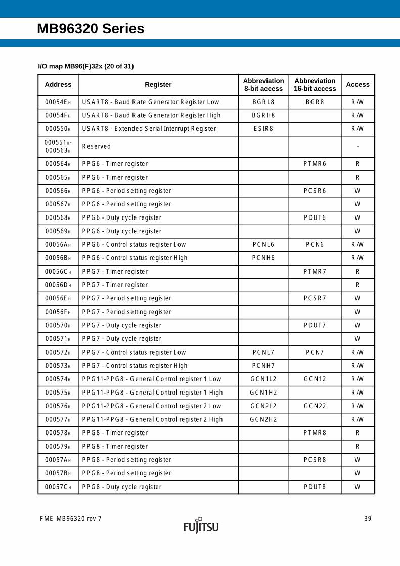
00054EH USART8 - Baud Rate Generator Register Low BGRL8 BGR8 R/W
00054FH USART8 - Baud Rate Generator Register High BGRH8 R/W
000550H USART8 - Extended Serial Interrupt Register ESIR8 R/W
000551H-000563H
Reserved -
000564H PPG6 - Timer register PTMR6 R
000565H PPG6 - Timer register R
000566H PPG6 - Period setting register PCSR6 W
000567H PPG6 - Period setting register W
000568H PPG6 - Duty cycle register PDUT6 W
000569H PPG6 - Duty cycle register W
00056AH PPG6 - Control status register Low PCNL6 PCN6 R/W
00056BH PPG6 - Control status register High PCNH6 R/W
00056CH PPG7 - Timer register PTMR7 R
00056DH PPG7 - Timer register R
00056EH PPG7 - Period setting register PCSR7 W
00056FH PPG7 - Period setting register W
000570H PPG7 - Duty cycle register PDUT7 W
000571H PPG7 - Duty cycle register W
000572H PPG7 - Control status register Low PCNL7 PCN7 R/W
000573H PPG7 - Control status register High PCNH7 R/W
000574H PPG11-PPG8 - General Control register 1 Low GCN1L2 GCN12 R/W
000575H PPG11-PPG8 - General Control register 1 High GCN1H2 R/W
000576H PPG11-PPG8 - General Control register 2 Low GCN2L2 GCN22 R/W
000577H PPG11-PPG8 - General Control register 2 High GCN2H2 R/W
000578H PPG8 - Timer register PTMR8 R
000579H PPG8 - Timer register R
00057AH PPG8 - Period setting register PCSR8 W
00057BH PPG8 - Period setting register W
00057CH PPG8 - Duty cycle register PDUT8 W
I/O map MB96(F)32x (20 of 31)
Address Register Abbreviation8-bit access
Abbreviation16-bit access Access
FME-MB96320 rev 7 39

MB96320 Series
00057DH PPG8 - Duty cycle register W
00057EH PPG8 - Control status register Low PCNL8 PCN8 R/W
00057FH PPG8 - Control status register High PCNH8 R/W
000580H PPG9 - Timer register PTMR9 R
000581H PPG9 - Timer register R
000582H PPG9 - Period setting register PCSR9 W
000583H PPG9 - Period setting register W
000584H PPG9 - Duty cycle register PDUT9 W
000585H PPG9 - Duty cycle register W
000586H PPG9 - Control status register Low PCNL9 PCN9 R/W
000587H PPG9 - Control status register High PCNH9 R/W
000588H PPG10 - Timer register PTMR10 R
000589H PPG10 - Timer register R
00058AH PPG10 - Period setting register PCSR10 W
00058BH PPG10 - Period setting register W
00058CH PPG10 - Duty cycle register PDUT10 W
00058DH PPG10 - Duty cycle register W
00058EH PPG10 - Control status register Low PCNL10 PCN10 R/W
00058FH PPG10 - Control status register High PCNH10 R/W
000590H PPG11 - Timer register PTMR11 R
000591H PPG11 - Timer register R
000592H PPG11 - Period setting register PCSR11 W
000593H PPG11 - Period setting register W
000594H PPG11 - Duty cycle register PDUT11 W
000595H PPG11 - Duty cycle register W
000596H PPG11 - Control status register Low PCNL11 PCN11 R/W
000597H PPG11 - Control status register High PCNH11 R/W
000598H PPG15-PPG12 - General Control register 1 Low GCN1L3 GCN13 R/W
000599H PPG15-PPG12 - General Control register 1 High GCN1H3 R/W
00059AH PPG15-PPG12 - General Control register 2 Low GCN2L3 GCN23 R/W
I/O map MB96(F)32x (21 of 31)
Address Register Abbreviation8-bit access
Abbreviation16-bit access Access
40 FME-MB96320 rev 7

MB96320 Series
00059BH PPG15-PPG12 - General Control register 2 High GCN2H3 R/W
00059CH PPG12 - Timer register PTMR12 R
00059DH PPG12 - Timer register R
00059EH PPG12 - Period setting register PCSR12 W
00059FH PPG12 - Period setting register W
0005A0H PPG12 - Duty cycle register PDUT12 W
0005A1H PPG12 - Duty cycle register W
0005A2H PPG12 - Control status register Low PCNL12 PCN12 R/W
0005A3H PPG12 - Control status register High PCNH12 R/W
0005A4H PPG13 - Timer register PTMR13 R
0005A5H PPG13 - Timer register R
0005A6H PPG13 - Period setting register PCSR13 W
0005A7H PPG13 - Period setting register W
0005A8H PPG13 - Duty cycle register PDUT13 W
0005A9H PPG13 - Duty cycle register W
0005AAH PPG13 - Control status register Low PCNL13 PCN13 R/W
0005ABH PPG13 - Control status register High PCNH13 R/W
0005ACH PPG14 - Timer register PTMR14 R
0005ADH PPG14 - Timer register R
0005AEH PPG14 - Period setting register PCSR14 W
0005AFH PPG14 - Period setting register W
0005B0H PPG14 - Duty cycle register PDUT14 W
0005B1H PPG14 - Duty cycle register W
0005B2H PPG14 - Control status register Low PCNL14 PCN14 R/W
0005B3H PPG14 - Control status register High PCNH14 R/W
0005B4H PPG15 - Timer register PTMR15 R
0005B5H PPG15 - Timer register R
0005B6H PPG15 - Period setting register PCSR15 W
0005B7H PPG15 - Period setting register W
0005B8H PPG15 - Duty cycle register PDUT15 W
I/O map MB96(F)32x (22 of 31)
Address Register Abbreviation8-bit access
Abbreviation16-bit access Access
FME-MB96320 rev 7 41

MB96320 Series
0005B9H PPG15 - Duty cycle register W
0005BAH PPG15 - Control status register Low PCNL15 PCN15 R/W
0005BBH PPG15 - Control status register High PCNH15 R/W
0005BCH PPG19-PPG16 - General Control register 1 Low GCN1L4 GCN14 R/W
0005BDH PPG19-PPG16 - General Control register 1 High GCN1H4 R/W
0005BEH PPG19-PPG16 - General Control register 2 Low GCN2L4 GCN24 R/W
0005BFH PPG19-PPG16 - General Control register 2 High GCN2H4 R/W
0005C0H PPG16 - Timer register PTMR16 R
0005C1H PPG16 - Timer register R
0005C2H PPG16 - Period setting register PCSR16 W
0005C3H PPG16 - Period setting register W
0005C4H PPG16 - Duty cycle register PDUT16 W
0005C5H PPG16 - Duty cycle register W
0005C6H PPG16 - Control status register Low PCNL16 PCN16 R/W
0005C7H PPG16 - Control status register High PCNH16 R/W
0005C8H PPG17 - Timer register PTMR17 R
0005C9H PPG17 - Timer register R
0005CAH PPG17 - Period setting register PCSR17 W
0005CBH PPG17 - Period setting register W
0005CCH PPG17 - Duty cycle register PDUT17 W
0005CDH PPG17 - Duty cycle register W
0005CEH PPG17 - Control status register Low PCNL17 PCN17 R/W
0005CFH PPG17 - Control status register High PCNH17 R/W
0005D0H PPG18 - Timer register PTMR18 R
0005D1H PPG18 - Timer register R
0005D2H PPG18 - Period setting register PCSR18 W
0005D3H PPG18 - Period setting register W
0005D4H PPG18 - Duty cycle register PDUT18 W
0005D5H PPG18 - Duty cycle register W
0005D6H PPG18 - Control status register Low PCNL18 PCN18 R/W
I/O map MB96(F)32x (23 of 31)
Address Register Abbreviation8-bit access
Abbreviation16-bit access Access
42 FME-MB96320 rev 7

MB96320 Series
0005D7H PPG18 - Control status register High PCNH18 R/W
0005D8H PPG19 - Timer register PTMR19 R
0005D9H PPG19 - Timer register R
0005DAH PPG19 - Period setting register PCSR19 W
0005DBH PPG19 - Period setting register W
0005DCH PPG19 - Duty cycle register PDUT19 W
0005DDH PPG19 - Duty cycle register W
0005DEH PPG19 - Control status register Low PCNL19 PCN19 R/W
0005DFH PPG19 - Control status register High PCNH19 R/W
0005E0H-00065FH
Reserved -
000660H Peripheral Resource Relocation Register 10 PRRR10 R/W
000661H Peripheral Resource Relocation Register 11 PRRR11 R/W
000662H Peripheral Resource Relocation Register 12 PRRR12 R/W
000663H Peripheral Resource Relocation Register 13 PRRR13 W
000664H-0006DFH
Reserved -
0006E0H External Bus - Area configuration register 0 Low EACL0 EAC0 R/W
0006E1H External Bus - Area configuration register 0 High EACH0 R/W
0006E2H External Bus - Area configuration register 1 Low EACL1 EAC1 R/W
0006E3H External Bus - Area configuration register 1 High EACH1 R/W
0006E4H External Bus - Area configuration register 2 Low EACL2 EAC2 R/W
0006E5H External Bus - Area configuration register 2 High EACH2 R/W
0006E6H External Bus - Area configuration register 3 Low EACL3 EAC3 R/W
0006E7H External Bus - Area configuration register 3 High EACH3 R/W
0006E8H External Bus - Area configuration register 4 Low EACL4 EAC4 R/W
0006E9H External Bus - Area configuration register 4 High EACH4 R/W
0006EAH External Bus - Area configuration register 5 Low EACL5 EAC5 R/W
0006EBH External Bus - Area configuration register 5 High EACH5 R/W
0006ECH External Bus - Area select register 2 EAS2 R/W
0006EDH External Bus - Area select register 3 EAS3 R/W
I/O map MB96(F)32x (24 of 31)
Address Register Abbreviation8-bit access
Abbreviation16-bit access Access
FME-MB96320 rev 7 43

MB96320 Series
0006EEH External Bus - Area select register 4 EAS4 R/W
0006EFH External Bus - Area select register 5 EAS5 R/W
0006F0H External Bus - Mode register EBM R/W
0006F1H External Bus - Clock and Function register EBCF R/W
0006F2H External Bus - Address output enable register 0 EBAE0 R/W
0006F3H External Bus - Address output enable register 1 EBAE1 R/W
0006F4H External Bus - Address output enable register 2 EBAE2 R/W
0006F5H External Bus - Control signal register EBCS R/W
0006F6H-0007FFH
Reserved -
000800H CAN1 - Control register Low CTRLRL1 CTRLR1 R/W
000801H CAN1 - Control register High (reserved) CTRLRH1 R
000802H CAN1 - Status register Low STATRL1 STATR1 R/W
000803H CAN1 - Status register High (reserved) STATRH1 R
000804H CAN1 - Error Counter Low (Transmit) ERRCNTL1 ERRCNT1 R
000805H CAN1 - Error Counter High (Receive) ERRCNTH1 R
000806H CAN1 - Bit Timing Register Low BTRL1 BTR1 R/W
000807H CAN1 - Bit Timing Register High BTRH1 R/W
000808H CAN1 - Interrupt Register Low INTRL1 INTR1 R
000809H CAN1 - Interrupt Register High INTRH1 R
00080AH CAN1 - Test Register Low TESTRL1 TESTR1 R/W
00080BH CAN1 - Test Register High (reserved) TESTRH1 R
00080CH CAN1 - BRP Extension register Low BRPERL1 BRPER1 R/W
00080DH CAN1 - BRP Extension register High (reserved) BRPERH1 R
00080EH-00080FH
Reserved -
000810H CAN1 - IF1 Command request register Low IF1CREQL1 IF1CREQ1 R/W
000811H CAN1 - IF1 Command request register High IF1CREQH1 R/W
000812H CAN1 - IF1 Command Mask register Low IF1CMSKL1 IF1CMSK1 R/W
000813HCAN1 - IF1 Command Mask register High (re-served)
IF1CMSKH1 R
I/O map MB96(F)32x (25 of 31)
Address Register Abbreviation8-bit access
Abbreviation16-bit access Access
44 FME-MB96320 rev 7

MB96320 Series
000814H CAN1 - IF1 Mask 1 Register Low IF1MSK1L1 IF1MSK11 R/W
000815H CAN1 - IF1 Mask 1 Register High IF1MSK1H1 R/W
000816H CAN1 - IF1 Mask 2 Register Low IF1MSK2L1 IF1MSK21 R/W
000817H CAN1 - IF1 Mask 2 Register High IF1MSK2H1 R/W
000818H CAN1 - IF1 Arbitration 1 Register Low IF1ARB1L1 IF1ARB11 R/W
000819H CAN1 - IF1 Arbitration 1 Register High IF1ARB1H1 R/W
00081AH CAN1 - IF1 Arbitration 2 Register Low IF1ARB2L1 IF1ARB21 R/W
00081BH CAN1 - IF1 Arbitration 2 Register High IF1ARB2H1 R/W
00081CH CAN1 - IF1 Message Control Register Low IF1MCTRL1 IF1MCTR1 R/W
00081DH CAN1 - IF1 Message Control Register High IF1MCTRH1 R/W
00081EH CAN1 - IF1 Data A1 Low IF1DTA1L1 IF1DTA11 R/W
00081FH CAN1 - IF1 Data A1 High IF1DTA1H1 R/W
000820H CAN1 - IF1 Data A2 Low IF1DTA2L1 IF1DTA21 R/W
000821H CAN1 - IF1 Data A2 High IF1DTA2H1 R/W
000822H CAN1 - IF1 Data B1 Low IF1DTB1L1 IF1DTB11 R/W
000823H CAN1 - IF1 Data B1 High IF1DTB1H1 R/W
000824H CAN1 - IF1 Data B2 Low IF1DTB2L1 IF1DTB21 R/W
000825H CAN1 - IF1 Data B2 High IF1DTB2H1 R/W
000826H-00083FH
Reserved -
000840H CAN1 - IF2 Command request register Low IF2CREQL1 IF2CREQ1 R/W
000841H CAN1 - IF2 Command request register High IF2CREQH1 R/W
000842H CAN1 - IF2 Command Mask register Low IF2CMSKL1 IF2CMSK1 R/W
000843HCAN1 - IF2 Command Mask register High (re-served)
IF2CMSKH1 R
000844H CAN1 - IF2 Mask 1 Register Low IF2MSK1L1 IF2MSK11 R/W
000845H CAN1 - IF2 Mask 1 Register High IF2MSK1H1 R/W
000846H CAN1 - IF2 Mask 2 Register Low IF2MSK2L1 IF2MSK21 R/W
000847H CAN1 - IF2 Mask 2 Register High IF2MSK2H1 R/W
000848H CAN1 - IF2 Arbitration 1 Register Low IF2ARB1L1 IF2ARB11 R/W
000849H CAN1 - IF2 Arbitration 1 Register High IF2ARB1H1 R/W
I/O map MB96(F)32x (26 of 31)
Address Register Abbreviation8-bit access
Abbreviation16-bit access Access
FME-MB96320 rev 7 45

MB96320 Series
00084AH CAN1 - IF2 Arbitration 2 Register Low IF2ARB2L1 IF2ARB21 R/W
00084BH CAN1 - IF2 Arbitration 2 Register High IF2ARB2H1 R/W
00084CH CAN1 - IF2 Message Control Register Low IF2MCTRL1 IF2MCTR1 R/W
00084DH CAN1 - IF2 Message Control Register High IF2MCTRH1 R/W
00084EH CAN1 - IF2 Data A1 Low IF2DTA1L1 IF2DTA11 R/W
00084FH CAN1 - IF2 Data A1 High IF2DTA1H1 R/W
000850H CAN1 - IF2 Data A2 Low IF2DTA2L1 IF2DTA21 R/W
000851H CAN1 - IF2 Data A2 High IF2DTA2H1 R/W
000852H CAN1 - IF2 Data B1 Low IF2DTB1L1 IF2DTB11 R/W
000853H CAN1 - IF2 Data B1 High IF2DTB1H1 R/W
000854H CAN1 - IF2 Data B2 Low IF2DTB2L1 IF2DTB21 R/W
000855H CAN1 - IF2 Data B2 High IF2DTB2H1 R/W
000856H-00087FH
Reserved -
000880H CAN1 - Transmission Request 1 Register Low TREQR1L1 TREQR11 R
000881H CAN1 - Transmission Request 1 Register High TREQR1H1 R
000882H CAN1 - Transmission Request 2 Register Low TREQR2L1 TREQR21 R
000883H CAN1 - Transmission Request 2 Register High TREQR2H1 R
000884H-00088FH
Reserved -
000890H CAN1 - New Data 1 Register Low NEWDT1L1 NEWDT11 R
000891H CAN1 - New Data 1 Register High NEWDT1H1 R
000892H CAN1 - New Data 2 Register Low NEWDT2L1 NEWDT21 R
000893H CAN1 - New Data 2 Register High NEWDT2H1 R
000894H-00089FH
Reserved -
0008A0H CAN1 - Interrupt Pending 1 Register Low INTPND1L1 INTPND11 R
0008A1H CAN1 - Interrupt Pending 1 Register High INTPND1H1 R
0008A2H CAN1 - Interrupt Pending 2 Register Low INTPND2L1 INTPND21 R
0008A3H CAN1 - Interrupt Pending 2 Register High INTPND2H1 R
I/O map MB96(F)32x (27 of 31)
Address Register Abbreviation8-bit access
Abbreviation16-bit access Access
46 FME-MB96320 rev 7

MB96320 Series
0008A4H-0008AFH
Reserved -
0008B0H CAN1 - Message Valid 1 Register Low MSGVAL1L1 MSGVAL11 R
0008B1H CAN1 - Message Valid 1 Register High MSGVAL1H1 R
0008B2H CAN1 - Message Valid 2 Register Low MSGVAL2L1 MSGVAL21 R
0008B3H CAN1 - Message Valid 2 Register High MSGVAL2H1 R
0008B4H-0008CDH
Reserved -
0008CEH CAN1 - Output enable register COER1 R/W
0008CFH-0008FFH
Reserved -
000900H CAN2 - Control register Low CTRLRL2 CTRLR2 R/W
000901H CAN2 - Control register High (reserved) CTRLRH2 R
000902H CAN2 - Status register Low STATRL2 STATR2 R/W
000903H CAN2 - Status register High (reserved) STATRH2 R
000904H CAN2 - Error Counter Low (Transmit) ERRCNTL2 ERRCNT2 R
000905H CAN2 - Error Counter High (Receive) ERRCNTH2 R
000906H CAN2 - Bit Timing Register Low BTRL2 BTR2 R/W
000907H CAN2 - Bit Timing Register High BTRH2 R/W
000908H CAN2 - Interrupt Register Low INTRL2 INTR2 R
000909H CAN2 - Interrupt Register High INTRH2 R
00090AH CAN2 - Test Register Low TESTRL2 TESTR2 R/W
00090BH CAN2 - Test Register High (reserved) TESTRH2 R
00090CH CAN2 - BRP Extension register Low BRPERL2 BRPER2 R/W
00090DH CAN2 - BRP Extension register High (reserved) BRPERH2 R
00090EH-00090FH
Reserved -
000910H CAN2 - IF1 Command request register Low IF1CREQL2 IF1CREQ2 R/W
000911H CAN2 - IF1 Command request register High IF1CREQH2 R/W
000912H CAN2 - IF1 Command Mask register Low IF1CMSKL2 IF1CMSK2 R/W
000913HCAN2 - IF1 Command Mask register High (re-served)
IF1CMSKH2 R
I/O map MB96(F)32x (28 of 31)
Address Register Abbreviation8-bit access
Abbreviation16-bit access Access
FME-MB96320 rev 7 47

MB96320 Series
000914H CAN2 - IF1 Mask 1 Register Low IF1MSK1L2 IF1MSK12 R/W
000915H CAN2 - IF1 Mask 1 Register High IF1MSK1H2 R/W
000916H CAN2 - IF1 Mask 2 Register Low IF1MSK2L2 IF1MSK22 R/W
000917H CAN2 - IF1 Mask 2 Register High IF1MSK2H2 R/W
000918H CAN2 - IF1 Arbitration 1 Register Low IF1ARB1L2 IF1ARB12 R/W
000919H CAN2 - IF1 Arbitration 1 Register High IF1ARB1H2 R/W
00091AH CAN2 - IF1 Arbitration 2 Register Low IF1ARB2L2 IF1ARB22 R/W
00091BH CAN2 - IF1 Arbitration 2 Register High IF1ARB2H2 R/W
00091CH CAN2 - IF1 Message Control Register Low IF1MCTRL2 IF1MCTR2 R/W
00091DH CAN2 - IF1 Message Control Register High IF1MCTRH2 R/W
00091EH CAN2 - IF1 Data A1 Low IF1DTA1L2 IF1DTA12 R/W
00091FH CAN2 - IF1 Data A1 High IF1DTA1H2 R/W
000920H CAN2 - IF1 Data A2 Low IF1DTA2L2 IF1DTA22 R/W
000921H CAN2 - IF1 Data A2 High IF1DTA2H2 R/W
000922H CAN2 - IF1 Data B1 Low IF1DTB1L2 IF1DTB12 R/W
000923H CAN2 - IF1 Data B1 High IF1DTB1H2 R/W
000924H CAN2 - IF1 Data B2 Low IF1DTB2L2 IF1DTB22 R/W
000925H CAN2 - IF1 Data B2 High IF1DTB2H2 R/W
000926H-00093FH
Reserved -
000940H CAN2 - IF2 Command request register Low IF2CREQL2 IF2CREQ2 R/W
000941H CAN2 - IF2 Command request register High IF2CREQH2 R/W
000942H CAN2 - IF2 Command Mask register Low IF2CMSKL2 IF2CMSK2 R/W
000943HCAN2 - IF2 Command Mask register High (re-served)
IF2CMSKH2 R
000944H CAN2 - IF2 Mask 1 Register Low IF2MSK1L2 IF2MSK12 R/W
000945H CAN2 - IF2 Mask 1 Register High IF2MSK1H2 R/W
000946H CAN2 - IF2 Mask 2 Register Low IF2MSK2L2 IF2MSK22 R/W
000947H CAN2 - IF2 Mask 2 Register High IF2MSK2H2 R/W
000948H CAN2 - IF2 Arbitration 1 Register Low IF2ARB1L2 IF2ARB12 R/W
000949H CAN2 - IF2 Arbitration 1 Register High IF2ARB1H2 R/W
I/O map MB96(F)32x (29 of 31)
Address Register Abbreviation8-bit access
Abbreviation16-bit access Access
48 FME-MB96320 rev 7
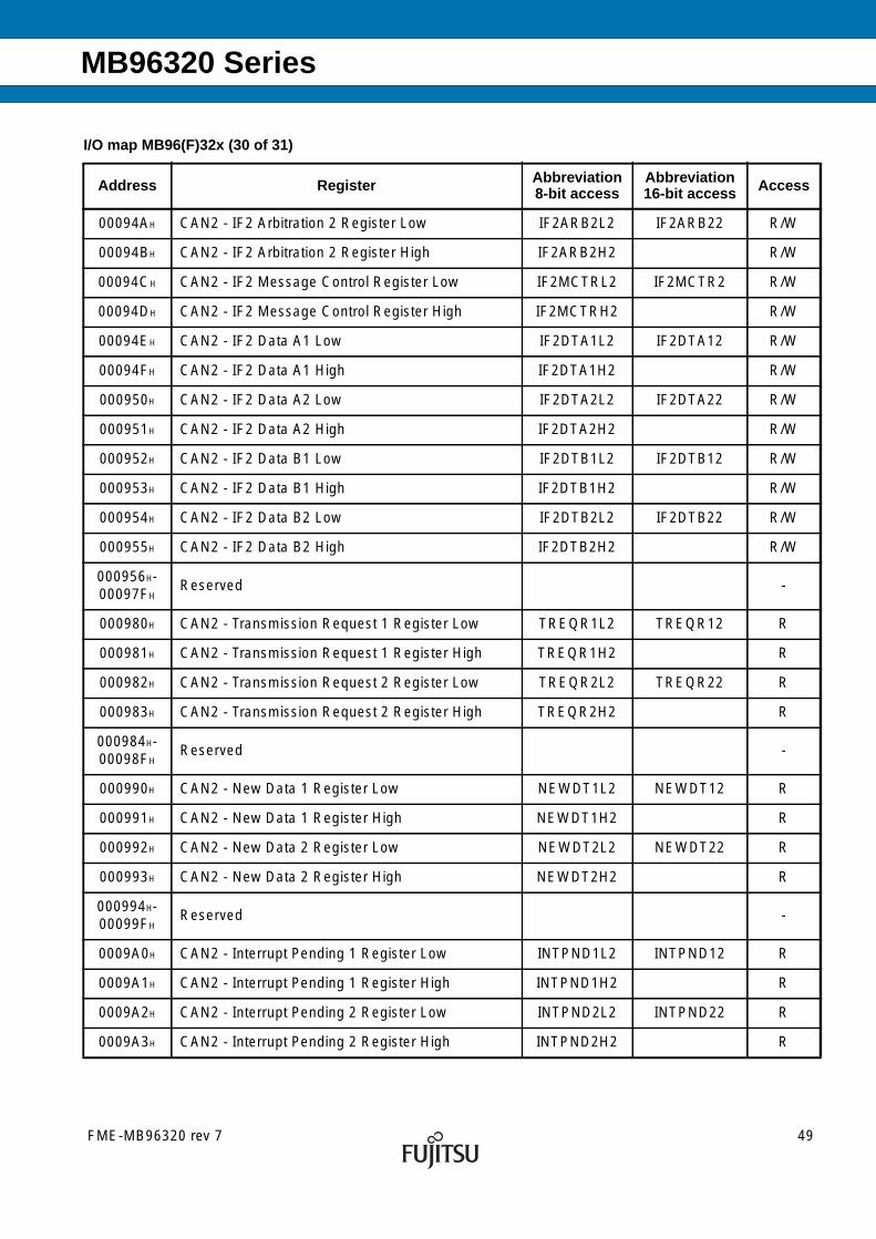
MB96320 Series
00094AH CAN2 - IF2 Arbitration 2 Register Low IF2ARB2L2 IF2ARB22 R/W
00094BH CAN2 - IF2 Arbitration 2 Register High IF2ARB2H2 R/W
00094CH CAN2 - IF2 Message Control Register Low IF2MCTRL2 IF2MCTR2 R/W
00094DH CAN2 - IF2 Message Control Register High IF2MCTRH2 R/W
00094EH CAN2 - IF2 Data A1 Low IF2DTA1L2 IF2DTA12 R/W
00094FH CAN2 - IF2 Data A1 High IF2DTA1H2 R/W
000950H CAN2 - IF2 Data A2 Low IF2DTA2L2 IF2DTA22 R/W
000951H CAN2 - IF2 Data A2 High IF2DTA2H2 R/W
000952H CAN2 - IF2 Data B1 Low IF2DTB1L2 IF2DTB12 R/W
000953H CAN2 - IF2 Data B1 High IF2DTB1H2 R/W
000954H CAN2 - IF2 Data B2 Low IF2DTB2L2 IF2DTB22 R/W
000955H CAN2 - IF2 Data B2 High IF2DTB2H2 R/W
000956H-00097FH
Reserved -
000980H CAN2 - Transmission Request 1 Register Low TREQR1L2 TREQR12 R
000981H CAN2 - Transmission Request 1 Register High TREQR1H2 R
000982H CAN2 - Transmission Request 2 Register Low TREQR2L2 TREQR22 R
000983H CAN2 - Transmission Request 2 Register High TREQR2H2 R
000984H-00098FH
Reserved -
000990H CAN2 - New Data 1 Register Low NEWDT1L2 NEWDT12 R
000991H CAN2 - New Data 1 Register High NEWDT1H2 R
000992H CAN2 - New Data 2 Register Low NEWDT2L2 NEWDT22 R
000993H CAN2 - New Data 2 Register High NEWDT2H2 R
000994H-00099FH
Reserved -
0009A0H CAN2 - Interrupt Pending 1 Register Low INTPND1L2 INTPND12 R
0009A1H CAN2 - Interrupt Pending 1 Register High INTPND1H2 R
0009A2H CAN2 - Interrupt Pending 2 Register Low INTPND2L2 INTPND22 R
0009A3H CAN2 - Interrupt Pending 2 Register High INTPND2H2 R
I/O map MB96(F)32x (30 of 31)
Address Register Abbreviation8-bit access
Abbreviation16-bit access Access
FME-MB96320 rev 7 49
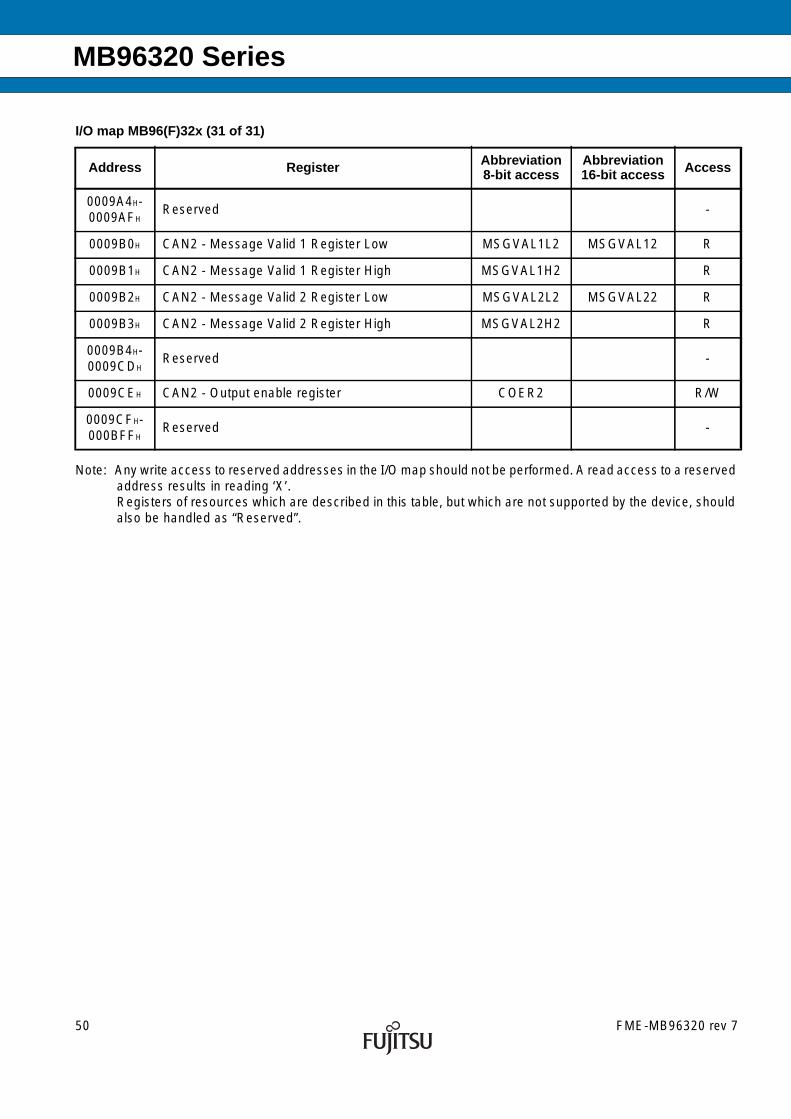
MB96320 Series
Note: Any write access to reserved addresses in the I/O map should not be performed. A read access to a reservedaddress results in reading ‘X’.Registers of resources which are described in this table, but which are not supported by the device, shouldalso be handled as “Reserved”.
0009A4H-0009AFH
Reserved -
0009B0H CAN2 - Message Valid 1 Register Low MSGVAL1L2 MSGVAL12 R
0009B1H CAN2 - Message Valid 1 Register High MSGVAL1H2 R
0009B2H CAN2 - Message Valid 2 Register Low MSGVAL2L2 MSGVAL22 R
0009B3H CAN2 - Message Valid 2 Register High MSGVAL2H2 R
0009B4H-0009CDH
Reserved -
0009CEH CAN2 - Output enable register COER2 R/W
0009CFH-000BFFH
Reserved -
I/O map MB96(F)32x (31 of 31)
Address Register Abbreviation8-bit access
Abbreviation16-bit access Access
50 FME-MB96320 rev 7

MB96320 Series
INTERRUPT VECTOR TABLE
Interrupt vector table MB96(F)32x (1 of 3)
Vectornumber
Offset invector ta-
bleVector name Clearedby
DMA
Index inICR to pro-
gramDescription
0 3FCH CALLV0 No -
1 3F8H CALLV1 No -
2 3F4H CALLV2 No -
3 3F0H CALLV3 No -
4 3ECH CALLV4 No -
5 3E8H CALLV5 No -
6 3E4H CALLV6 No -
7 3E0H CALLV7 No -
8 3DCH RESET No -
9 3D8H INT9 No -
10 3D4H EXCEPTION No -
11 3D0H NMI No - Non-Maskable Interrupt
12 3CCH DLY No 12 Delayed Interrupt
13 3C8H RC_TIMER No 13 RC Timer
14 3C4H MC_TIMER No 14 Main Clock Timer
15 3C0H SC_TIMER No 15 Sub Clock Timer
16 3BCH PLL_UNLOCK No 16 Reserved
17 3B8H EXTINT0 Yes 17 External Interrupt 0
18 3B4H EXTINT1 Yes 18 External Interrupt 1
19 3B0H EXTINT2 Yes 19 External Interrupt 2
20 3ACH EXTINT3 Yes 20 External Interrupt 3
21 3A8H EXTINT4 Yes 21 External Interrupt 4
22 3A4H EXTINT5 Yes 22 External Interrupt 5
23 3A0H EXTINT7 Yes 23 External Interrupt 7
24 39CH EXTINT8 Yes 24 External Interrupt 8
25 398H EXTINT9 Yes 25 External Interrupt 9
26 394H EXTINT10 Yes 26 External Interrupt 10
27 390H EXTINT11 Yes 27 External Interrupt 11
28 38CH EXTINT12 Yes 28 External Interrupt 12
29 388H EXTINT13 Yes 29 External Interrupt 13
30 384H EXTINT14 Yes 30 External Interrupt 14
31 380H EXTINT15 Yes 31 External Interrupt 15
32 37CH CAN1 No 32 CAN Controller 1
FME-MB96320 rev 7 51

MB96320 Series
33 378H CAN2 No 33 CAN Controller 2
34 374H PPG0 Yes 34 Programmable Pulse Generator 0
35 370H PPG1 Yes 35 Programmable Pulse Generator 1
36 36CH PPG2 Yes 36 Programmable Pulse Generator 2
37 368H PPG3 Yes 37 Programmable Pulse Generator 3
38 364H PPG4 Yes 38 Programmable Pulse Generator 4
39 360H PPG5 Yes 39 Programmable Pulse Generator 5
40 35CH PPG6 Yes 40 Programmable Pulse Generator 6
41 358H PPG7 Yes 41 Programmable Pulse Generator 7
42 354H PPG8 Yes 42 Programmable Pulse Generator 8
43 350H PPG9 Yes 43 Programmable Pulse Generator 9
44 34CH PPG10 Yes 44 Programmable Pulse Generator 10
45 348H PPG11 Yes 45 Programmable Pulse Generator 11
46 344H PPG12 Yes 46 Programmable Pulse Generator 12
47 340H PPG13 Yes 47 Programmable Pulse Generator 13
48 33CH PPG14 Yes 48 Programmable Pulse Generator 14
49 338H PPG15 Yes 49 Programmable Pulse Generator 15
50 334H PPG16 Yes 50 Programmable Pulse Generator 16
51 330H PPG17 Yes 51 Programmable Pulse Generator 17
52 32CH PPG18 Yes 52 Programmable Pulse Generator 18
53 328H PPG19 Yes 53 Programmable Pulse Generator 19
54 324H RLT0 Yes 54 Reload Timer 0
55 320H RLT1 Yes 55 Reload Timer 1
56 31CH RLT2 Yes 56 Reload Timer 2
57 318H RLT3 Yes 57 Reload Timer 3
58 314H PPGRLT Yes 58 Reload Timer 6 - dedicated for PPG
59 310H ICU0 Yes 59 Input Capture Unit 0
60 30CH ICU1 Yes 60 Input Capture Unit 1
61 308H ICU2 Yes 61 Input Capture Unit 2
62 304H ICU3 Yes 62 Input Capture Unit 3
63 300H ICU4 Yes 63 Input Capture Unit 4
64 2FCH ICU5 Yes 64 Input Capture Unit 5
65 2F8H ICU6 Yes 65 Input Capture Unit 6
66 2F4H ICU7 Yes 66 Input Capture Unit 7
67 2F0H ICU8 Yes 67 Input Capture Unit 8
Interrupt vector table MB96(F)32x (2 of 3)
Vectornumber
Offset invector ta-
bleVector name Clearedby
DMA
Index inICR to pro-
gramDescription
52 FME-MB96320 rev 7

MB96320 Series
68 2ECH ICU9 Yes 68 Input Capture Unit 9
69 2E8H ICU10 Yes 69 Input Capture Unit 10
70 2E4H ICU11 Yes 70 Input Capture Unit 11
71 2E0H OCU4 Yes 71 Output Compare Unit 4
72 2DCH OCU5 Yes 72 Output Compare Unit 5
73 2D8H OCU6 Yes 73 Output Compare Unit 6
74 2D4H OCU7 Yes 74 Output Compare Unit 7
75 2D0H OCU10 Yes 75 Output Compare Unit 10
76 2CCH OCU11 Yes 76 Output Compare Unit 11
77 2C8H FRT0 Yes 77 Free Running Timer 0
78 2C4H FRT1 Yes 78 Free Running Timer 1
79 2C0H FRT2 Yes 79 Free Running Timer 2
80 2BCH FRT3 Yes 80 Free Running Timer 3
81 2B8H RTC0 No 81 Real Timer Clock
82 2B4H CAL0 No 82 Clock Calibration Unit
83 2B0H IIC0 Yes 83 I2C interface
84 2ACH ADC0 Yes 84 A/D Converter
85 2A8H LINR2 Yes 85 LIN USART 2 RX
86 2A4H LINT2 Yes 86 LIN USART 2 TX
87 2A0H LINR3 Yes 87 LIN USART 3 RX
88 29CH LINT3 Yes 88 LIN USART 3 TX
89 298H LINR7 Yes 89 LIN USART 7 RX
90 294H LINT7 Yes 90 LIN USART 7 TX
91 290H LINR8 Yes 91 LIN USART 8 RX
92 28CH LINT8 Yes 92 LIN USART 8 TX
93 288H FLASH_A No 93 Flash memory A (only Flash devices)
Interrupt vector table MB96(F)32x (3 of 3)
Vectornumber
Offset invector ta-
bleVector name Clearedby
DMA
Index inICR to pro-
gramDescription
FME-MB96320 rev 7 53
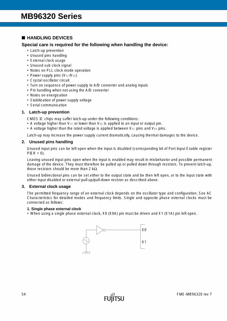
MB96320 Series
HANDLING DEVICES
Special care is required for the following when handling the device:• Latch-up prevention• Unused pins handling• External clock usage• Unused sub clock signal• Notes on PLL clock mode operation• Power supply pins (VCC/VSS)• Crystal oscillator circuit• Turn on sequence of power supply to A/D converter and analog inputs• Pin handling when not using the A/D converter• Notes on energization• Stabilization of power supply voltage• Serial communication
1. Latch-up prevention
CMOS IC chips may suffer latch-up under the following conditions:• A voltage higher than VCC or lower than VSS is applied to an input or output pin.• A voltage higher than the rated voltage is applied between VCC pins and VSS pins.
Latch-up may increase the power supply current dramatically, causing thermal damages to the device.
2. Unused pins handling
Unused input pins can be left open when the input is disabled (corresponding bit of Port Input Enable registerPIER = 0).
Leaving unused input pins open when the input is enabled may result in misbehavior and possible permanentdamage of the device. They must therefore be pulled up or pulled down through resistors. To prevent latch-up,those resistors should be more than 2 kΩ.
Unused bidirectional pins can be set either to the output state and be then left open, or to the input state witheither input disabled or external pull-up/pull-down resistor as described above.
3. External clock usage
The permitted frequency range of an external clock depends on the oscillator type and configuration. See ACCharacteristics for detailed modes and frequency limits. Single and opposite phase external clocks must beconnected as follows:
1. Single phase external clock• When using a single phase external clock, X0 (X0A) pin must be driven and X1 (X1A) pin left open.
X0
X1
54 FME-MB96320 rev 7

MB96320 Series
2. Opposite phase external clock• When using an opposite phase external clock, X1 (X1A) must be supplied with a clock signal which has the
opposite phase to the X0 (X0A) pins.
4. Unused sub clock signal
If the pins X0A and X1A are not connected to an oscillator, a pull-down resistor must be connected on the X0Apin and the X1A pin must be left open.
5. Notes on PLL clock mode operation
If the PLL clock mode is selected and no external oscillator is operating or no external clock is supplied, themicrocontroller attempts to work with the free oscillating PLL. Performance of this operation, however, cannotbe guaranteed.
6. Power supply pins (VCC/VSS)
It is required that all VCC-level as well as all VSS-level power supply pins are at the same potential. If there is morethan one VCC or VSS level, the device may operate incorrectly or be damaged even within the guaranteed operatingrange.
VCC and VSS must be connected to the device from the power supply with lowest possible impedance.
As a measure against power supply noise, it is required to connect a bypass capacitor of about 0.1 µF betweenVCC and VSS as close as possible to VCC and VSS pins.
7. Crystal oscillator and ceramic resonator circuit
Noise at X0, X1 pins or X0A, X1A pins might cause abnormal operation. It is required to provide bypass capacitorswith shortest possible distance to X0, X1 pins and X0A, X1A pins, crystal oscillator (or ceramic resonator) andground lines, and, to the utmost effort, that the lines of oscillation circuit do not cross the lines of other circuits.
It is highly recommended to provide a printed circuit board art work surrounding X0, X1 pins and X0A, X1A pinswith a ground area for stabilizing the operation.
It is highly recommended to evaluate the quartz/MCU or resonator/MCU system at the quartz or resonatormanufacturer, especially when using low-Q resonators at higher frequencies.
8. Turn on sequence of power supply to A/D converter and analog inputs
It is required to turn the A/D converter power supply (AVCC, AVRH, AVRL) and analog inputs (ANn) on afterturning the digital power supply (VCC) on.
It is also required to turn the digital power off after turning the A/D converter supply and analog inputs off. In thiscase, the voltage must not exceed AVRH or AVCC (turning the analog and digital power supplies simultaneouslyon or off is acceptable).
9. Pin handling when not using the A/D converter
It is required to connect the unused pins of the A/D converter as AVCC = VCC, AVSS = AVRH = AVRL = VSS.
10. Notes on Power-on
To prevent malfunction of the internal voltage regulator, supply voltage profile while turning the power supply onshould be slower than 50µs from 0.2 V to 2.7 V.
X0
X1
FME-MB96320 rev 7 55
MB96320 Series
11. Stabilization of power supply voltage
If the power supply voltage varies acutely even within the operation safety range of the Vcc power supply voltage,a malfunction may occur. The Vcc power supply voltage must therefore be stabilized. As stabilization guidelines,the power supply voltage must be stabilized in such a way that Vcc ripple fluctuations (peak to peak value) inthe commercial frequencies (50 to 60 Hz) fall within 10% of the standard Vcc power supply voltage and thetransient fluctuation rate becomes 0.1V/µs or less in instantaneous fluctuation for power supply switching.
12. Serial communication
There is a possibility to receive wrong data due to noise or other causes on the serial communication.Therefore, design a printed circuit board so as to avoid noise.Consider receiving of wrong data when designing the system. For example apply a checksum and retransmitthe data if an error occurs.
56 FME-MB96320 rev 7

MB96320 Series
ELECTRICAL CHARACTERISTICS
1. Absolute Maximum Ratings
*1: AVCC and VCC must be set to the same voltage. It is required that AVCC does not exceed VCC and that the voltageat the analog inputs does not exceed AVCC neither when the power is switched on.
Parameter SymbolRating
Unit RemarksMin Max
Power supply voltageVCC VSS - 0.3 VSS + 6.0 V
AVCC VSS - 0.3 VSS + 6.0 V VCC = AVCC *1
AD Converter voltage references AVRH,AVRL VSS - 0.3 VSS + 6.0 V AVCC ≥ AVRH, AVCC ≥ AVRL,
AVRH > AVRL, AVRL ≥ AVSS
Input voltage VI VSS - 0.3 VSS + 6.0 V VI ≤ VCC + 0.3V *2
Output voltage VO VSS - 0.3 VSS + 6.0 V VO ≤ VCC + 0.3V *2
Maximum Clamp Current ICLAMP -4.0 +4.0 mA Applicable to general purposeI/O pins *3
Total Maximum Clamp Current Σ|ICLAMP| - 40 mA Applicable to general purposeI/O pins *3
“L” level maximum output current IOL1 - 15 mA Normal outputs with drivingstrength set to 5mA
“L” level average output current IOLAV1 - 5 mA Normal outputs with drivingstrength set to 5mA
“L” level maximum overall output current ΣIOL1 - 100 mA Normal outputs
“L” level average overall output current ΣIOLAV1 - 50 mA Normal outputs
”H” level maximum output current IOH1 - -15 mA Normal outputs with drivingstrength set to 5mA
”H” level average output current IOHAV1 - -5 mA Normal outputs with drivingstrength set to 5mA
”H” level maximum overall output current ΣIOH1 - -100 mA Normal outputs
”H” level average overall output current ΣIOHAV1 - -50 mA Normal outputs
Permitted Power dissipation (Flash de-vices) *4 PD
- 300*5 mW TA=105oC
- 600*5 mW TA=85oC
- 750*5 mW TA=75oC
- 375*5 mW TA=125oC, no Flash program/erase *6
- 530*5 mW TA=115oC, no Flash program/erase *6
Operating ambient temperature TA
0 +70oC
MB96V300B
-40 +105
-40 +125 *6
Storage temperature TSTG -55 +150 oC
FME-MB96320 rev 7 57
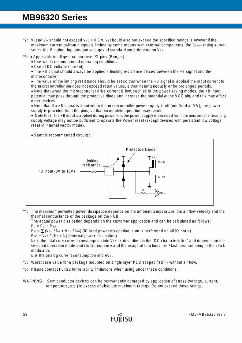
MB96320 Series
*2: VI and VO should not exceed VCC + 0.3 V. VI should also not exceed the specified ratings. However if themaximum current to/from a input is limited by some means with external components, the ICLAMP rating super-sedes the VI rating. Input/output voltages of standard ports depend on VCC.
*3: • Applicable to all general purpose I/O pins (Pnn_m)• Use within recommended operating conditions.• Use at DC voltage (current)• The +B signal should always be applied a limiting resistance placed between the +B signal and themicrocontroller.• The value of the limiting resistance should be set so that when the +B signal is applied the input current tothe microcontroller pin does not exceed rated values, either instantaneously or for prolonged periods.• Note that when the microcontroller drive current is low, such as in the power saving modes, the +B inputpotential may pass through the protective diode and increase the potential at the VCC pin, and this may affectother devices.• Note that if a +B signal is input when the microcontroller power supply is off (not fixed at 0 V), the powersupply is provided from the pins, so that incomplete operation may result.• Note that if the +B input is applied during power-on, the power supply is provided from the pins and the resultingsupply voltage may not be sufficient to operate the Power reset (except devices with persistent low voltagereset in internal vector mode).
• Sample recommended circuits:
*4: The maximum permitted power dissipation depends on the ambient temperature, the air flow velocity and thethermal conductance of the package on the PCB.The actual power dissipation depends on the customer application and can be calculated as follows:PD = PIO + PINT
PIO = ∑ (VOL * IOL + VOH * IOH) (IO load power dissipation, sum is performed on all IO ports)PINT = VCC * (ICC + IA) (internal power dissipation)ICC is the total core current consumption into VCC as described in the “DC characteristics” and depends on theselected operation mode and clock frequency and the usage of functions like Flash programming or the clockmodulator.IA is the analog current consumption into AVCC.
*5: Worst case value for a package mounted on single layer PCB at specified TA without air flow.
*6: Please contact Fujitsu for reliability limitations when using under these conditions.
WARNING: Semiconductor devices can be permanently damaged by application of stress (voltage, current,temperature, etc.) in excess of absolute maximum ratings. Do not exceed these ratings.
P-ch
N-ch
VCC
R
Protective Diode
Limitingresistance
+B input (0V to 16V)
58 FME-MB96320 rev 7
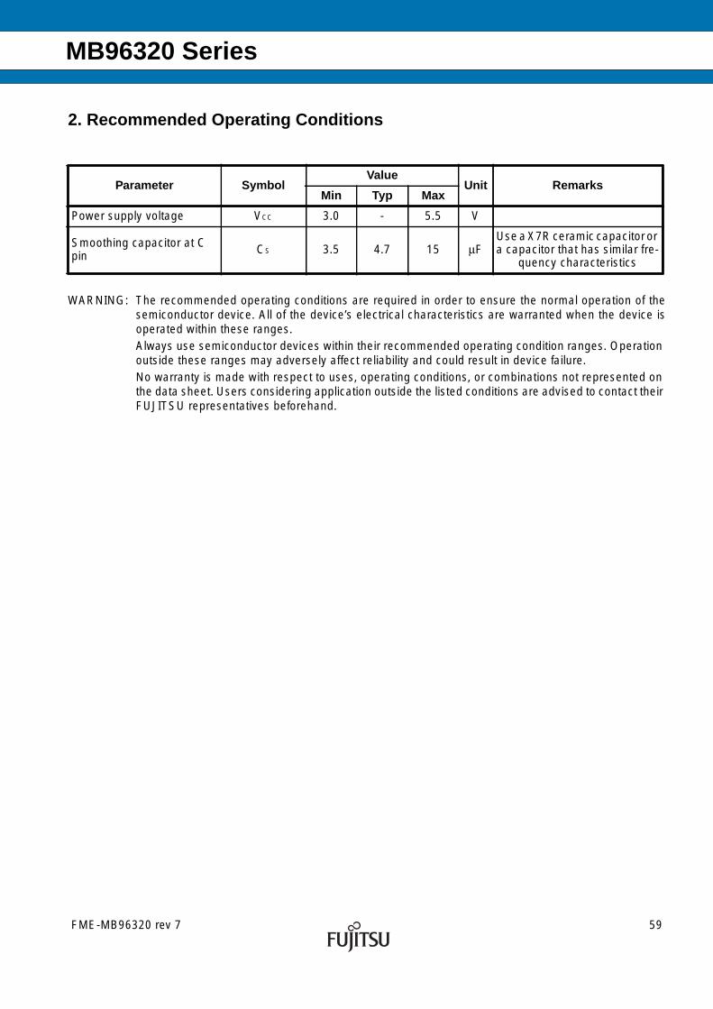
MB96320 Series
FME-MB96320 rev 7 59
2. Recommended Operating Conditions
WARNING: The recommended operating conditions are required in order to ensure the normal operation of thesemiconductor device. All of the device’s electrical characteristics are warranted when the device isoperated within these ranges.Always use semiconductor devices within their recommended operating condition ranges. Operationoutside these ranges may adversely affect reliability and could result in device failure.No warranty is made with respect to uses, operating conditions, or combinations not represented onthe data sheet. Users considering application outside the listed conditions are advised to contact theirFUJITSU representatives beforehand.
Parameter SymbolValue
Unit RemarksMin Typ Max
Power supply voltage VCC 3.0 - 5.5 V
Smoothing capacitor at Cpin CS 3.5 4.7 15 µF
Use a X7R ceramic capacitor ora capacitor that has similar fre-
quency characteristics

MB96320 Series
3. DC characteristics
(TA = -40˚C to 125˚C, VCC = AVCC = 3.0V to 5.5V, VSS = AVSS = 0V)
Parameter Symbol Pin ConditionValue
Unit RemarksMin Typ Max
Input H voltage
VIH
Port inputs
Pnn_m
CMOSHysteresis0.8/0.2 input se-lected
0.8VCC
- VCC +0.3 V
CMOSHysteresis0.7/0.3 input se-lected
0.7VCC
- VCC +0.3 V VCC ≥ 4.5V
0.74VCC
- VCC +0.3 V VCC < 4.5V
AUTOMOTIVEHysteresis inputselected
0.8VCC
- VCC +0.3 V
TTL input select-ed 2.0 - VCC +
0.3 V
VIHX0F X0External clock in“Fast Clock Input
mode”
0.8VCC
- VCC +0.3 V
VIHX0SX0,X1,
X0A,X1AExternal clock in“oscillation mode” 2.5 - VCC +
0.3 V
VIHR RSTX - 0.8VCC
- VCC +0.3 V CMOS Hysteresis in-
put
VIHM MD2-MD0 - VCC -0.3 - VCC +
0.3 V
Input L voltage
VIL
Port inputs
Pnn_m
CMOSHysteresis0.8/0.2 input se-lected
VSS -0.3 - 0.2
VCCV
CMOSHysteresis0.7/0.3 input se-lected
VSS -0.3 - 0.3
VCCV
AUTOMOTIVEHysteresis inputselected
VSS -0.3 - 0.5
VCCV VCC ≥ 4.5V
VSS -0.3 - 0.46
VCCVCC < 4.5V
TTL input select-ed
VSS -0.3 - 0.8 V
VILX0F X0External clock in“Fast Clock Input
mode”
VSS -0.3 - 0.2 VCC V
VILX0SX0,X1,
X0A,X1AExternal clock in“oscillation mode”
VSS -0.3 - 0.4 V
VILR RSTX - VSS -0.3 - 0.2 VCC V CMOS Hysteresis in-
put
VILM MD2-MD0 - VSS -0.3 - VSS +
0.3 V
60 FME-MB96320 rev 7
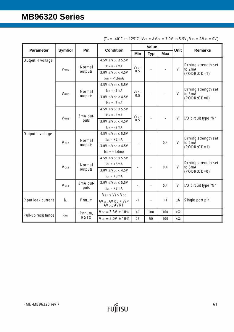
MB96320 Series
Output H voltage
VOH2Normaloutputs
4.5V ≤ VCC ≤ 5.5V
IOH = -2mA VCC -0.5 - - V
Driving strength setto 2mA(PODR:OD=1)3.0V ≤ VCC < 4.5V
IOH = -1.6mA
VOH5Normaloutputs
4.5V ≤ VCC ≤ 5.5V
IOH = -5mA VCC -0.5 - - V
Driving strength setto 5mA(PODR:OD=0)3.0V ≤ VCC < 4.5V
IOH = -3mA
VOH33mA out-
puts
4.5V ≤ VCC ≤ 5.5V
IOH = -3mA VCC -0.5 - - V I/O circuit type “N”
3.0V ≤ VCC < 4.5V
IOH = -2mA
Output L voltage
VOL2Normaloutputs
4.5V ≤ VCC ≤ 5.5V
IOL = +2mA- - 0.4 V
Driving strength setto 2mA(PODR:OD=1)3.0V ≤ VCC < 4.5V
IOL = +1.6mA
VOL5Normaloutputs
4.5V ≤ VCC ≤ 5.5V
IOL = +5mA- - 0.4 V
Driving strength setto 5mA(PODR:OD=0)3.0V ≤ VCC < 4.5V
IOL = +3mA
VOL33mA out-
puts3.0V ≤ VCC ≤ 5.5V
IOL = +3mA- - 0.4 V I/O circuit type “N”
Input leak current IIL Pnn_mVSS < VI < VCC
AVSS, AVRL < VI <AVCC, AVRH
-1 - +1 µA Single port pin
Pull-up resistance RUPPnn_m,RSTX
VCC = 3.3V ± 10% 40 100 160 kΩ
VCC = 5.0V ± 10% 25 50 100 kΩ
(TA = -40˚C to 125˚C, VCC = AVCC = 3.0V to 5.5V, VSS = AVSS = 0V)
Parameter Symbol Pin ConditionValue
Unit RemarksMin Typ Max
FME-MB96320 rev 7 61

MB96320 Series
(TA = -40˚C to 125˚C, VCC = AVCC = 3.0V to 5.5V, VSS = AVSS = 0V)
Parameter Symbol Condition (at TA)Value
RemarksTyp Max Unit
Power supply cur-rent in Runmodes*
ICCPLL
PLL Run mode withCLKS1/2 = CLKB =CLKP1 = 16MHz,CLKP2 = 8MHz
1 Flash/ROM wait state
(CLKRC and CLKSCstopped)
+25˚C 15 20
mA+125˚C 16.5 23.5
PLL Run mode withCLKS1/2 = CLKB =CLKP1 = 32MHz,CLKP2 = 16MHz
2 Flash/ROM wait states
(CLKRC and CLKSCstopped)
+25˚C 24 30
mA+125˚C 26 34
PLL Run mode withCLKS1/2 = 48MHz,CLKB = CLKP1/2 =
24MHz
0 Flash/ROM wait states
(CLKRC and CLKSCstopped)
+25˚C 28 40
mA+125˚C 30 44
PLL Run mode withCLKS1/2 = CLKB =
CLKP1= 56MHz,CLKP2 = 28MHz
2 Flash/ROM wait states
(CLKRC and CLKSCstopped. Core voltage at
1.9V)
+25˚C 41 52
mA+125˚C 43 56
PLL Run mode withCLKS1/2 = 96MHz,
CLKB = CLKP1= 48MHz,CLKP2 = 24MHz
1 Flash/ROM wait state
(CLKRC and CLKSCstopped. Core voltage at
1.9V)
+25˚C 44 58
mA+125˚C 46 62
62 FME-MB96320 rev 7

MB96320 Series
Power supply cur-rent in Runmodes*
ICCMAIN
Main Run mode withCLKS1/2 = CLKB =CLKP1/2 = 4MHz
1 Flash/ROM wait state
(CLKPLL, CLKSC andCLKRC stopped)
+25˚C 4.2 5.2
mA+125˚C 4.9 8.2
ICCRCH
RC Run mode withCLKS1/2 = CLKB =CLKP1/2 = 2MHz
1 Flash/ROM wait state
(CLKMC, CLKPLL andCLKSC stopped)
+25˚C 2.7 3.7
mA+125˚C 3.4 6.7
ICCRCL
RC Run mode withCLKS1/2 = CLKB =CLKP1/2 = 100kHz,
SMCR:LPMS = 0
1 Flash/ROM wait state
(CLKMC, CLKPLL andCLKSC stopped. Voltageregulator in high power
mode)
+25˚C 0.4 0.6
mA+125˚C 0.95 3.4
RC Run mode withCLKS1/2 = CLKB =CLKP1/2 = 100kHz,
SMCR:LPMS = 1
1 Flash/ROM wait state
(CLKMC, CLKPLL andCLKSC stopped. Voltage
regulator in low powermode, no Flash program-
ming/erasing allowed)
+25˚C 0.15 0.25
mA+125˚C 0.7 3.05
ICCSUB
Sub Run mode withCLKS1/2 = CLKB =CLKP1/2 = 32kHz
1 Flash/ROM wait state
(CLKMC, CLKPLL andCLKRC stopped, no Flashprogramming/erasing al-
lowed)
+25˚C 0.1 0.2
mA+125˚C 0.65 3
(TA = -40˚C to 125˚C, VCC = AVCC = 3.0V to 5.5V, VSS = AVSS = 0V)
Parameter Symbol Condition (at TA)Value
RemarksTyp Max Unit
FME-MB96320 rev 7 63

MB96320 Series
Power supply cur-rent in Sleepmodes*
ICCSPLL
PLL Sleep mode withCLKS1/2 = CLKP1 =
16MHz,CLKP2 = 8MHz
(CLKRC and CLKSCstopped)
+25˚C 4 6
mA+125˚C 4.7 9
PLL Sleep mode withCLKS1/2 = CLKP1 =
32MHz,CLKP2 = 16MHz
(CLKRC and CLKSCstopped)
+25˚C 7 9.5
mA+125˚C 8 12.5
PLL Sleep mode withCLKS1/2 = 48MHz,CLKP1/2 = 24MHz
(CLKRC and CLKSCstopped)
+25˚C 7 9
mA+125˚C 8 12
PLL Sleep mode withCLKS1/2 = CLKP1=
56MHz, CLKP2 = 28MHz
(CLKRC and CLKSCstopped. Core voltage at
1.9V)
+25˚C 11 14.5
mA+125˚C 12 17.5
PLL Sleep mode withCLKS1/2 = 96MHz,CLKP1= 48MHz,CLKP2 = 24MHz
(CLKRC and CLKSCstopped. Core voltage at
1.9V)
+25˚C 12 15
mA+125˚C 13 18
ICCSMAIN
Main Sleep mode withCLKS1/2 = CLKP1/2 =
4MHz
(CLKPLL, CLKSC andCLKRC stopped)
+25˚C 1.3 1.8
mA+125˚C 1.9 4.6
ICCSRCH
RC Sleep mode withCLKS1/2 = CLKP1/2 =
2MHz
(CLKMC, CLKPLL andCLKSC stopped)
+25˚C 0.8 1.4
mA+125˚C 1.4 4.2
(TA = -40˚C to 125˚C, VCC = AVCC = 3.0V to 5.5V, VSS = AVSS = 0V)
Parameter Symbol Condition (at TA)Value
RemarksTyp Max Unit
64 FME-MB96320 rev 7

MB96320 Series
Power supply cur-rent in Sleepmodes*
ICCSRCL
RC Sleep mode withCLKS1/2 = CLKP1/2 =
100kHz,SMCR:LPMSS = 0
(CLKMC, CLKPLL andCLKSC stopped. Voltageregulator in high power
mode)
+25˚C 0.3 0.5
mA+125˚C 0.8 3.3
RC Sleep mode withCLKS1/2 = CLKP1/2 =
100kHz,SMCR:LPMSS = 1
(CLKMC, CLKPLL andCLKSC stopped. Voltage
regulator in low powermode)
+25˚C 0.05 0.15
mA+125˚C 0.56 2.9
ICCSSUB
Sub Sleep mode withCLKS1/2 = CLKP1/2 =
32kHz
(CLKMC, CLKPLL andCLKRC stopped)
+25˚C 0.04 0.12
mA+125˚C 0.54 2.9
Power supply cur-rent in Timermodes*
ICCTPLL
PLL Timer mode withCLKMC = 4MHz, CLKPLL
= 48MHz
(CLKRC and CLKSCstopped)
+25˚C 1.5 2
mA+125˚C 2.1 5
ICCTMAIN
Main Timer mode withCLKMC = 4MHz,
SMCR:LPMSS = 0
(CLKPLL, CLKRC andCLKSC stopped. Voltageregulator in high power
mode)
+25˚C 0.35 0.5
mA+125˚C 0.85 3.3
Main Timer mode withCLKMC = 4MHz,
SMCR:LPMSS = 1
(CLKPLL, CLKRC andCLKSC stopped. Voltage
regulator in low powermode)
+25˚C 0.08 0.15
mA+125˚C 0.6 2.9
(TA = -40˚C to 125˚C, VCC = AVCC = 3.0V to 5.5V, VSS = AVSS = 0V)
Parameter Symbol Condition (at TA)Value
RemarksTyp Max Unit
FME-MB96320 rev 7 65

MB96320 Series
Power supply cur-rent in Timermodes*
ICCTRCH
RC Timer mode withCLKRC = 2MHz,
SMCR:LPMSS = 0
(CLKMC, CLKPLL andCLKSC stopped. Voltageregulator in high power
mode)
+25˚C 0.35 0.5
mA+125˚C 0.85 3.3
RC Timer mode withCLKRC = 2MHz,
SMCR:LPMSS = 1
(CLKMC, CLKPLL andCLKSC stopped. Voltage
regulator in low powermode)
+25˚C 0.07 0.15
mA+125˚C 0.6 2.9
ICCTRCL
RC Timer mode withCLKRC = 100kHz,SMCR:LPMSS = 0
(CLKMC, CLKPLL andCLKSC stopped. Voltageregulator in high power
mode)
+25˚C 0.3 0.45
mA+125˚C 0.8 3.2
RC Timer mode withCLKRC = 100kHz,SMCR:LPMSS = 1
(CLKMC, CLKPLL andCLKSC stopped. Voltage
regulator in low powermode)
+25˚C 0.03 0.1
mA+125˚C 0.53 2.85
ICCTSUB
Sub Timer mode withCLKSC = 32kHz
(CLKMC, CLKPLL andCLKRC stopped)
+25˚C 0.035 0.1
mA+125˚C 0.53 2.85
Power supply cur-rent in Stop Mode ICCH
VRCR:LPMB[2:0] = 110B
(Core voltage at 1.8V)
+25˚C 0.02 0.08mA
+125˚C 0.52 2.8
VRCR:LPMB[2:0] = 000B
(Core voltage at 1.2V)
+25˚C 0.015 0.06mA
+125˚C 0.4 2.3
Power supply cur-rent for active LowVoltage detector
ICCLVDLow voltage detector en-abled (RCR:LVDE = 1)
+25˚C 90 140µA Must be added to all
current above+125˚C 100 150
Power supply cur-rent for activeClock modulator
ICCCLOMOClock modulator enabled
(CMCR:PDX = 1) - 3 4.5 mA Must be added to allcurrent above
(TA = -40˚C to 125˚C, VCC = AVCC = 3.0V to 5.5V, VSS = AVSS = 0V)
Parameter Symbol Condition (at TA)Value
RemarksTyp Max Unit
66 FME-MB96320 rev 7

MB96320 Series
FlashWrite/Erasecurrent ICCFLASH
Current for one Flashmodule - 15 40 mA Must be added to all
current above
Input capacitance CIN - - 5 15 pFOther than C, AVCC,AVSS, AVRH, AVRL,VCC, VSS
* The power supply current is measured with a 4MHz external clock connected to the Main oscillator and a 32kHzexternal clock connected to the Sub oscillator. See chapter “Standby mode and voltage regulator control circuit” ofthe Hardware Manual for further details about voltage regulator control.
(TA = -40˚C to 125˚C, VCC = AVCC = 3.0V to 5.5V, VSS = AVSS = 0V)
Parameter Symbol Condition (at TA)Value
RemarksTyp Max Unit
FME-MB96320 rev 7 67
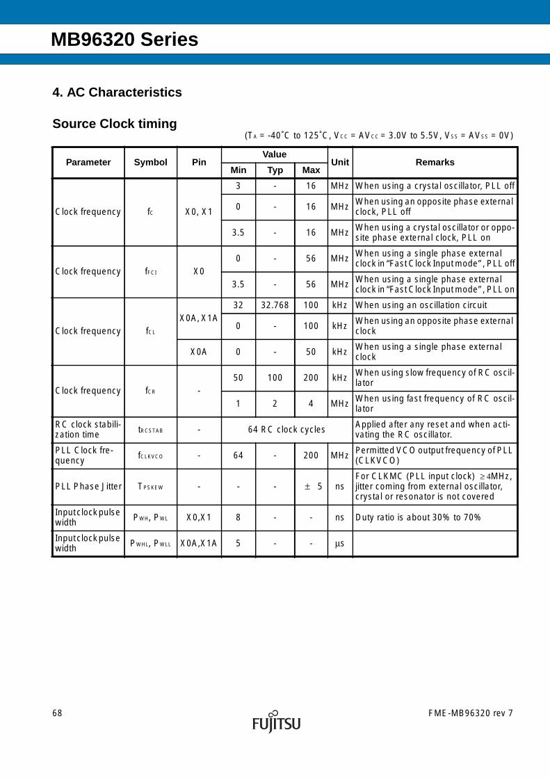
MB96320 Series
4. AC Characteristics
Source Clock timing(TA = -40˚C to 125˚C, VCC = AVCC = 3.0V to 5.5V, VSS = AVSS = 0V)
Parameter Symbol PinValue
Unit RemarksMin Typ Max
Clock frequency fC X0, X1
3 - 16 MHz When using a crystal oscillator, PLL off
0 - 16 MHz When using an opposite phase externalclock, PLL off
3.5 - 16 MHz When using a crystal oscillator or oppo-site phase external clock, PLL on
Clock frequency fFCI X00 - 56 MHz When using a single phase external
clock in “Fast Clock Input mode” , PLL off
3.5 - 56 MHz When using a single phase externalclock in “Fast Clock Input mode” , PLL on
Clock frequency fCL
X0A, X1A32 32.768 100 kHz When using an oscillation circuit
0 - 100 kHz When using an opposite phase externalclock
X0A 0 - 50 kHz When using a single phase externalclock
Clock frequency fCR -50 100 200 kHz When using slow frequency of RC oscil-
lator
1 2 4 MHz When using fast frequency of RC oscil-lator
RC clock stabili-zation time tRCSTAB - 64 RC clock cycles Applied after any reset and when acti-
vating the RC oscillator.
PLL Clock fre-quency fCLKVCO - 64 - 200 MHz Permitted VCO output frequency of PLL
(CLKVCO)
PLL Phase Jitter TPSKEW - - - ± 5 nsFor CLKMC (PLL input clock) ≥ 4MHz,jitter coming from external oscillator,crystal or resonator is not covered
Inputclockpulsewidth PWH, PWL X0,X1 8 - - ns Duty ratio is about 30% to 70%
Inputclockpulsewidth PWHL, PWLL X0A,X1A 5 - - µs
68 FME-MB96320 rev 7
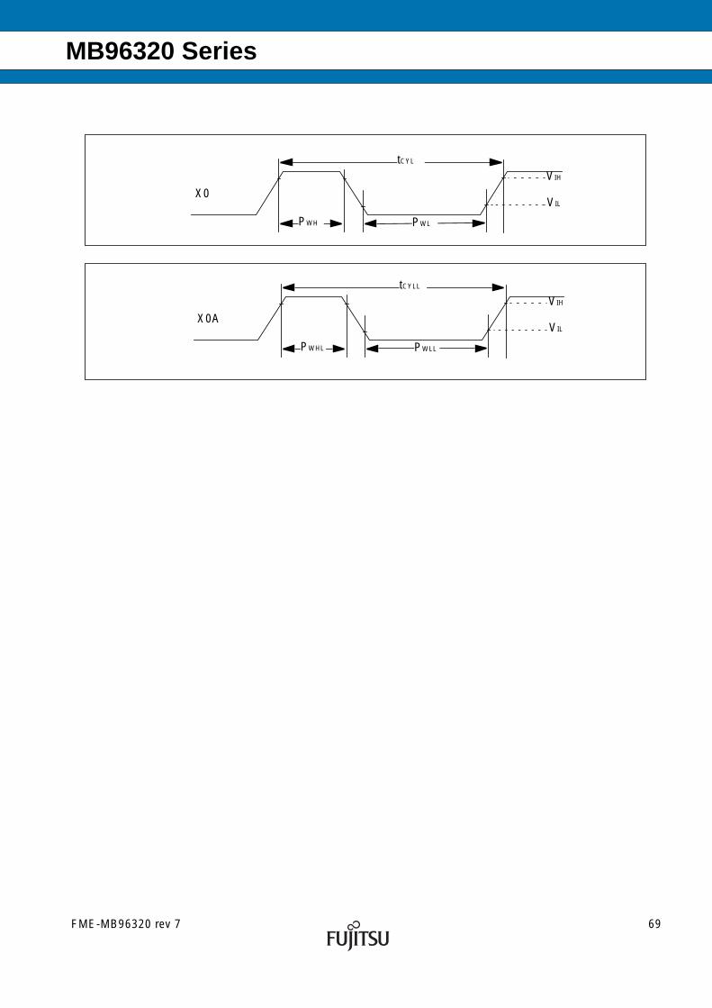
MB96320 Series
X0
tCYL
PWH PWL
VIL
VIH
X0A
tCYLL
PWHL PWLL
VIL
VIH
FME-MB96320 rev 7 69

MB96320 Series
70 FME-MB96320 rev 7
Internal Clock timing(TA = -40˚C to 125˚C, VCC = AVCC = 3.0V to 5.5V, VSS = AVSS = 0V)
Parameter Symbol
Core Voltage Settings
Unit Remarks1.8V 1.9V
Min Max Min Max
Internal System clock fre-quency (CLKS1 andCLKS2)
fCLKS1, fCLKS2 0 92 0 96 MHz Others than below
0 88 0 96 MHz MB96F326
Internal CPU clock fre-quency (CLKB), internalperipheralclock frequency(CLKP1)
fCLKB, fCLKP1 0 52 0 56 MHz
Internal peripheral clockfrequency (CLKP2) fCLKP2 0 28 0 32 MHz

MB96320 Series
FME-MB96320 rev 7 71
External Reset timing(TA = -40˚C to 125˚C, VCC = AVCC = 3.0V to 5.5V, VSS = AVSS = 0V)
Parameter Symbol PinValue
Unit RemarksMin Typ Max
Reset input time tRSTL RSTX 500 - - ns
0.2 VCC
RSTX
tRSTL
0.2 VCC

MB96320 Series
72 FME-MB96320 rev 7
Power On Reset timing(TA = -40˚C to 125˚C, VCC = AVCC = 3.0V to 5.5V, VSS = AVSS = 0V)
Parameter Symbol PinValue
Unit RemarksMin Typ Max
Power on rise time tR Vcc 0.05 - 30 ms
Power off time tOFF Vcc 1 - - ms
0.2 V
tR
2.7V
tOFF
0.2 V 0.2 V
If the power supply is changed too rapidly, a power-on reset may occur.We recommend a smooth startup by restraining voltages when changing thepower supply voltage during operation, as shown in the figure below.
3 V
VCC
VCC
Rising edge of 50 mV/msmaximum is allowed

MB96320 Series
FME-MB96320 rev 7 73
External Input timing
Note : Relocated Resource Inputs have same characteristics
(TA = -40˚C to 125˚C, VCC = AVCC = 3.0V to 5.5V, VSS = AVSS = 0V)
Parameter Symbol Pin ConditionValue
Unit Used Pin input func-tionMin Max
Input pulsewidth
tINH
tINL
INTn(_R)
⎯
200 ⎯ nsExternal Interrupt
NMI(_R) NMI
Pnn_m
2*tCLKP1 + 200(tCLKP1=1/
fCLKP1)⎯ ns
General Purpose IO
TINn(_R) Reload Timer
TTGn(_R) PPG Trigger input
ADTG(_R) AD Converter Trigger
FRCKn(_R)Free Running Timer
external clock
INn(_R) Input Capture
VIL
VIH
tINH
VIL
VIH
tINL
External Pin input

MB96320 Series
External Bus timing
Note: The values given below are for an I/O driving strength IOdrive = 5mA. If IOdrive is 2mA, all the maximum outputtiming described in the different tables must then be increased by 10ns.
Basic Timing(TA = −40 °C to +125 °C, VCC = 5.0 V ± 10%, VSS = 0.0 V, IOdrive = 5mA, CL = 50pF)
Parameter Symbol Pin ConditionValue
Unit RemarksMin Max
ECLK
tCYC
ECLK ⎯
25 ⎯
nstCHCL tCYC/2-5 tCYC/2+5
tCLCH tCYC/2-5 tCYC/2+5
ECLK →UBX/ LBX / CSn time
tCHCBH
CSn, UBX,LBX, ECLK
⎯
-20 20
nstCHCBL -20 20
tCLCBH -20 20
tCLCBL -20 20
ECLK → ALE time
tCHLH
ALE, ECLK ⎯
-10 10
nstCHLL -10 10
tCLLH -10 10
tCLLL -10 10
ECLK → address valid time
tCHAV A[23:16],ECLK
⎯-15 15
nstCLAV -15 15
tCLADV AD[15:0],ECLK
⎯-15 15
nstCHADV -15 15
ECLK → RDX /WRX time
tCHRWH
RDX, WRX,WRLX,WRHX,ECLK
⎯
-10 10
nstCHRWL -10 10
tCLRWH -10 10
tCLRWL -10 10
74 FME-MB96320 rev 7

MB96320 Series
(TA = −40 °C to +125 °C, VCC = 3.0 to 4.5V, VSS = 0.0 V, IOdrive = 5mA, CL = 50pF)
Parameter Symbol Pin ConditionValue
Unit RemarksMin Max
ECLK
tCYC
ECLK ⎯
30 ⎯
nstCHCL tCYC/2-8 tCYC/2+8
tCLCH tCYC/2-8 tCYC/2+8
ECLK →UBX/ LBX / CSn time
tCHCBH
CSn, UBX,LBX, ECLK
⎯
-25 25
nstCHCBL -25 25
tCLCBH -25 25
tCLCBL -25 25
ECLK → ALE time
tCHLH
ALE, ECLK ⎯
-15 15
nstCHLL -15 15
tCLLH -15 15
tCLLL -15 15
ECLK → address valid time
tCHAV A[23:16],ECLK
⎯-20 20
nstCLAV -20 20
tCLADV AD[15:0],ECLK
⎯-20 20
nstCHADV -20 20
ECLK → RDX /WRX time
tCHRWH
RDX, WRX,WRLX, WRHX,ECLK
⎯
-15 15
nstCHRWL -15 15
tCLRWH -15 15
tCLRWL -15 15
FME-MB96320 rev 7 75

MB96320 Series
ECLK
tCYC
CSn
ALE
A[23:16]
0.2*Vcc
tCHCL
tCHAV
tCHCBL tCHCBH
LBX UBX
tCLLHtCHLL tCHLH
tCLLL
tCLADV
AD[15:0] Address
tCLAV
tCHADV
tCLCBH tCLCBL
tCHRWHtCLRWH tCLRWLtCHRWL
RDX
WRX (WRLX, WRHX)
0.8*Vcc
tCLCH
Refer to the Hardware Manual for detailed Timing Charts
76 FME-MB96320 rev 7
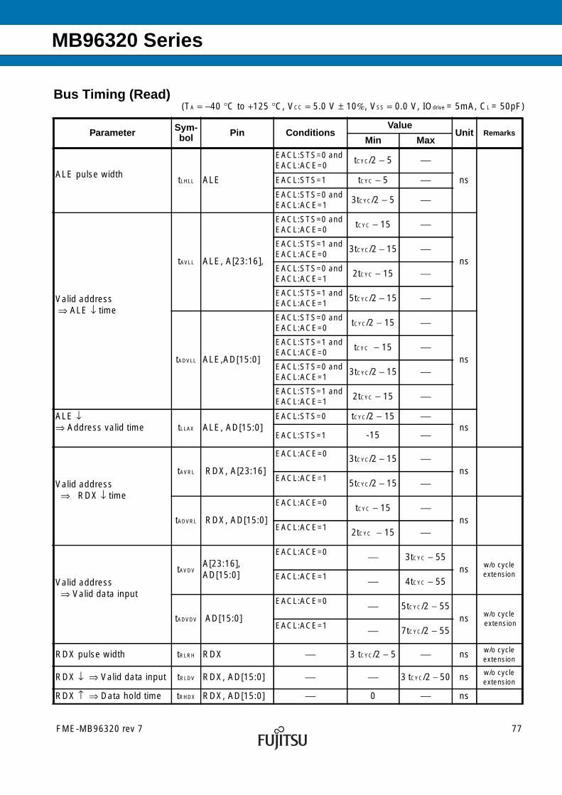
MB96320 Series
Bus Timing (Read)(TA = −40 °C to +125 °C, VCC = 5.0 V ± 10%, VSS = 0.0 V, IOdrive = 5mA, CL = 50pF)
Parameter Sym-bol Pin Conditions
ValueUnit Remarks
Min Max
ALE pulse widthtLHLL ALE
EACL:STS=0 andEACL:ACE=0
tCYC/2 − 5 ⎯
nsEACL:STS=1 tCYC − 5 ⎯EACL:STS=0 andEACL:ACE=1
3tCYC/2 − 5 ⎯
Valid address⇒ ALE ↓ time
tAVLL ALE, A[23:16],
EACL:STS=0 andEACL:ACE=0
tCYC − 15 ⎯
ns
EACL:STS=1 andEACL:ACE=0
3tCYC/2 − 15 ⎯
EACL:STS=0 andEACL:ACE=1
2tCYC − 15 ⎯
EACL:STS=1 andEACL:ACE=1
5tCYC/2 − 15 ⎯
tADVLL ALE,AD[15:0]
EACL:STS=0 andEACL:ACE=0
tCYC/2 − 15 ⎯
ns
EACL:STS=1 andEACL:ACE=0
tCYC − 15 ⎯
EACL:STS=0 andEACL:ACE=1
3tCYC/2 − 15 ⎯
EACL:STS=1 andEACL:ACE=1
2tCYC − 15 ⎯
ALE ↓⇒ Address valid time tLLAX ALE, AD[15:0]
EACL:STS=0 tCYC/2 − 15 ⎯ns
EACL:STS=1 -15 ⎯
Valid address⇒ RDX ↓ time
tAVRL RDX, A[23:16]
EACL:ACE=0 3tCYC/2 − 15 ⎯ns
EACL:ACE=1 5tCYC/2 − 15 ⎯
tADVRL RDX, AD[15:0]
EACL:ACE=0 tCYC − 15 ⎯ns
EACL:ACE=1 2tCYC − 15 ⎯
Valid address⇒ Valid data input
tAVDVA[23:16],AD[15:0]
EACL:ACE=0 ⎯ 3tCYC − 55ns w/o cycle
extensionEACL:ACE=1 ⎯ 4tCYC − 55
tADVDV AD[15:0]
EACL:ACE=0 ⎯ 5tCYC/2 − 55ns w/o cycle
extensionEACL:ACE=1 ⎯ 7tCYC/2 − 55
RDX pulse width tRLRH RDX ⎯ 3 tCYC/2 − 5 ⎯ ns w/o cycleextension
RDX ↓ ⇒ Valid data input tRLDV RDX, AD[15:0] ⎯ ⎯ 3 tCYC/2 − 50 ns w/o cycleextension
RDX ↑ ⇒ Data hold time tRHDX RDX, AD[15:0] ⎯ 0 ⎯ ns
FME-MB96320 rev 7 77

MB96320 Series
Address valid ⇒ Data holdtime
tAXDXA[23:16],AD[15:0]
⎯ 0 ⎯ ns
RDX ↑ ⇒ ALE ↑ time tRHLH RDX, ALE
EACL:STS=1 andEACL:ACE=1
3tCYC/2 − 10 ⎯ns
other ECL:STS,EACL:ACE setting
tCYC/2 − 10 ⎯
Valid address⇒ ECLK ↑ time
tAVCH A[23:16], ECLK⎯
tCYC − 15 ⎯ns
tADVCH AD[15:0], ECLK tCYC/2 − 15 ⎯RDX ↓ ⇒ ECLK ↑ time tRLCH RDX, ECLK ⎯ tCYC/2 − 10 ⎯ ns
ALE ↓ ⇒ RDX ↓ time tLLRL ALE, RDXEACL:STS=0 tCYC/2 − 10 ⎯
nsEACL:STS=1 − 10 ⎯
ECLK↑ ⇒ Valid data input tCHDV AD[15:0], ECLK ⎯ ⎯ tCYC − 50 ns
(TA = −40 °C to +125 °C, VCC = 3.0 to 4.5V, VSS = 0.0 V, IOdrive = 5mA, CL = 50pF)
Parameter Sym-bol Pin Conditions
ValueUnit Remarks
Min Max
ALE pulse widthtLHLL ALE
EACL:STS=0 andEACL:ACE=0
tCYC/2 − 8 ⎯
nsEACL:STS=1 tCYC − 8 ⎯EACL:STS=0 andEACL:ACE=1
3tCYC/2 − 8 ⎯
Valid address⇒ ALE ↓ time
tAVLL ALE, A[23:16],
EACL:STS=0 andEACL:ACE=0
tCYC − 20 ⎯
ns
EACL:STS=1 andEACL:ACE=0
3tCYC/2 − 20 ⎯
EACL:STS=0 andEACL:ACE=1
2tCYC − 20 ⎯
EACL:STS=1 andEACL:ACE=1
5tCYC/2 − 20 ⎯
tADVLL ALE, AD[15:0]
EACL:STS=0 andEACL:ACE=0
tCYC/2 − 20 ⎯
ns
EACL:STS=1 andEACL:ACE=0
tCYC − 20 ⎯
EACL:STS=0 andEACL:ACE=1
3tCYC/2 − 20 ⎯
EACL:STS=1 andEACL:ACE=1
2tCYC − 20 ⎯
ALE ↓⇒ Address valid time tLLAX ALE, AD[15:0]
EACL:STS=0 tCYC/2 − 20 ⎯ns
EACL:STS=1 -20 ⎯
(TA = −40 °C to +125 °C, VCC = 5.0 V ± 10%, VSS = 0.0 V, IOdrive = 5mA, CL = 50pF)
Parameter Sym-bol Pin Conditions
ValueUnit Remarks
Min Max
78 FME-MB96320 rev 7
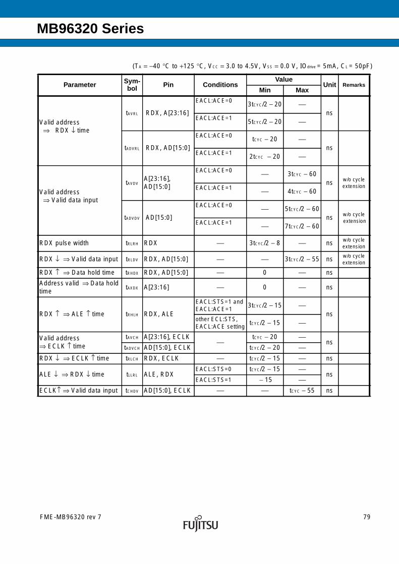
MB96320 Series
Valid address⇒ RDX ↓ time
tAVRL RDX, A[23:16]
EACL:ACE=0 3tCYC/2 − 20 ⎯ns
EACL:ACE=1 5tCYC/2 − 20 ⎯
tADVRL RDX, AD[15:0]
EACL:ACE=0 tCYC − 20 ⎯ns
EACL:ACE=1 2tCYC − 20 ⎯
Valid address⇒ Valid data input
tAVDVA[23:16],AD[15:0]
EACL:ACE=0 ⎯ 3tCYC − 60ns w/o cycle
extensionEACL:ACE=1 ⎯ 4tCYC − 60
tADVDV AD[15:0]
EACL:ACE=0 ⎯ 5tCYC/2 − 60ns w/o cycle
extensionEACL:ACE=1 ⎯ 7tCYC/2 − 60
RDX pulse width tRLRH RDX ⎯ 3tCYC/2 − 8 ⎯ ns w/o cycleextension
RDX ↓ ⇒ Valid data input tRLDV RDX, AD[15:0] ⎯ ⎯ 3tCYC/2 − 55 ns w/o cycleextension
RDX ↑ ⇒ Data hold time tRHDX RDX, AD[15:0] ⎯ 0 ⎯ ns
Address valid ⇒ Data holdtime
tAXDX A[23:16] ⎯ 0 ⎯ ns
RDX ↑ ⇒ ALE ↑ time tRHLH RDX, ALE
EACL:STS=1 andEACL:ACE=1
3tCYC/2 − 15 ⎯ns
other ECL:STS,EACL:ACE setting
tCYC/2 − 15 ⎯
Valid address⇒ ECLK ↑ time
tAVCH A[23:16], ECLK⎯
tCYC − 20 ⎯ns
tADVCH AD[15:0], ECLK tCYC/2 − 20 ⎯RDX ↓ ⇒ ECLK ↑ time tRLCH RDX, ECLK ⎯ tCYC/2 − 15 ⎯ ns
ALE ↓ ⇒ RDX ↓ time tLLRL ALE, RDXEACL:STS=0 tCYC/2 − 15 ⎯
nsEACL:STS=1 − 15 ⎯
ECLK↑ ⇒ Valid data input tCHDV AD[15:0], ECLK ⎯ ⎯ tCYC − 55 ns
(TA = −40 °C to +125 °C, VCC = 3.0 to 4.5V, VSS = 0.0 V, IOdrive = 5mA, CL = 50pF)
Parameter Sym-bol Pin Conditions
ValueUnit Remarks
Min Max
FME-MB96320 rev 7 79
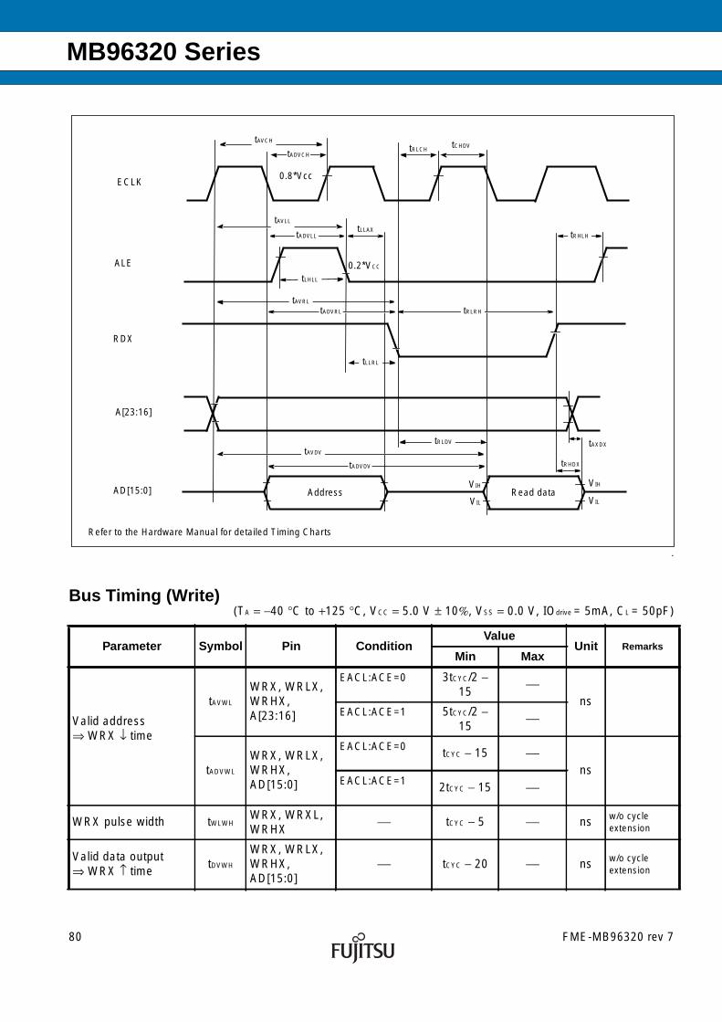
MB96320 Series
.
Bus Timing (Write)(TA = −40 °C to +125 °C, VCC = 5.0 V ± 10%, VSS = 0.0 V, IOdrive = 5mA, CL = 50pF)
Parameter Symbol Pin ConditionValue
Unit RemarksMin Max
Valid address⇒ WRX ↓ time
tAVWL
WRX, WRLX,WRHX,A[23:16]
EACL:ACE=0 3tCYC/2 −15
⎯ns
EACL:ACE=1 5tCYC/2 −15
⎯
tADVWL
WRX, WRLX,WRHX,AD[15:0]
EACL:ACE=0 tCYC − 15 ⎯ns
EACL:ACE=1 2tCYC − 15 ⎯
WRX pulse width tWLWHWRX, WRXL,WRHX
⎯ tCYC − 5 ⎯ ns w/o cycleextension
Valid data output⇒ WRX ↑ time
tDVWH
WRX, WRLX,WRHX,AD[15:0]
⎯ tCYC − 20 ⎯ ns w/o cycleextension
A[23:16]
AD[15:0] AddressVIL
VIH VIH
VIL
Read data
tRHDX
tRLDV
tADVDV
ECLK
tADVCH
0.8*Vcc
tRLCH
ALE
tLHLL
tRHLH
0.2*VCC
tLLAXtADVLL
RDX
tLLRL
tRLRHtADVRL
tAVCH
tAVLL
tAVDV
tAVRL
tCHDV
tAXDX
Refer to the Hardware Manual for detailed Timing Charts
80 FME-MB96320 rev 7
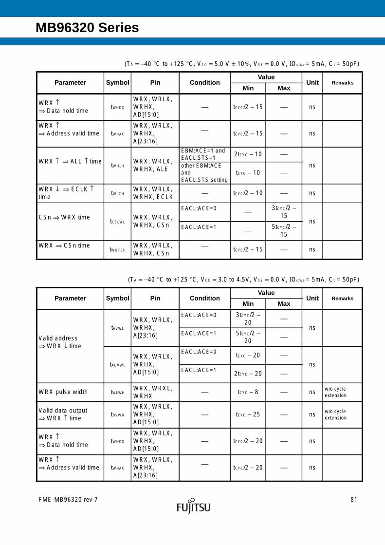
MB96320 Series
WRX ↑⇒ Data hold time
tWHDX
WRX, WRLX,WRHX,AD[15:0]
⎯ tCYC/2 − 15 ⎯ ns
WRX ↑⇒ Address valid time tWHAX
WRX, WRLX,WRHX,A[23:16]
⎯ tCYC/2 − 15 ⎯ ns
WRX ↑ ⇒ ALE ↑ timetWHLH
WRX, WRLX,WRHX, ALE
EBM:ACE=1 andEACL:STS=1
2tCYC − 10 ⎯
nsother EBM:ACEandEACL:STS setting
tCYC − 10 ⎯
WRX ↓ ⇒ ECLK ↑time
tWLCHWRX, WRLX,WRHX, ECLK
⎯ tCYC/2 − 10 ⎯ ns
CSn ⇒ WRX timetCSLWL
WRX, WRLX,WRHX, CSn
EACL:ACE=0 ⎯ 3tCYC/2 −15
nsEACL:ACE=1 ⎯ 5tCYC/2 −
15
WRX ⇒ CSn timetWHCSH
WRX, WRLX,WRHX, CSn
⎯ tCYC/2 − 15 ⎯ ns
(TA = −40 °C to +125 °C, VCC = 3.0 to 4.5V, VSS = 0.0 V, IOdrive = 5mA, CL = 50pF)
Parameter Symbol Pin ConditionValue
Unit RemarksMin Max
Valid address⇒ WRX ↓ time
tAVWL
WRX, WRLX,WRHX,A[23:16]
EACL:ACE=0 3tCYC/2 −20
⎯ns
EACL:ACE=1 5tCYC/2 −20
⎯
tADVWL
WRX, WRLX,WRHX,AD[15:0]
EACL:ACE=0 tCYC − 20 ⎯ns
EACL:ACE=1 2tCYC − 20 ⎯
WRX pulse width tWLWHWRX, WRXL,WRHX
⎯ tCYC − 8 ⎯ ns w/o cycleextension
Valid data output⇒ WRX ↑ time
tDVWH
WRX, WRLX,WRHX,AD[15:0]
⎯ tCYC − 25 ⎯ ns w/o cycleextension
WRX ↑⇒ Data hold time
tWHDX
WRX, WRLX,WRHX,AD[15:0]
⎯ tCYC/2 − 20 ⎯ ns
WRX ↑⇒ Address valid time tWHAX
WRX, WRLX,WRHX,A[23:16]
⎯ tCYC/2 − 20 ⎯ ns
(TA = −40 °C to +125 °C, VCC = 5.0 V ± 10%, VSS = 0.0 V, IOdrive = 5mA, CL = 50pF)
Parameter Symbol Pin ConditionValue
Unit RemarksMin Max
FME-MB96320 rev 7 81
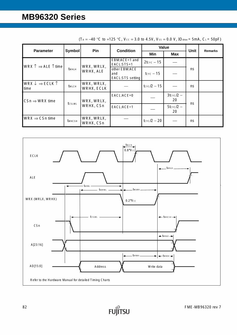
MB96320 Series
.
WRX ↑ ⇒ ALE ↑ timetWHLH
WRX, WRLX,WRHX, ALE
EBM:ACE=1 andEACL:STS=1
2tCYC − 15 ⎯
nsother EBM:ACEandEACL:STS setting
tCYC − 15 ⎯
WRX ↓ ⇒ ECLK ↑time
tWLCHWRX, WRLX,WRHX, ECLK
⎯ tCYC/2 − 15 ⎯ ns
CSn ⇒ WRX timetCSLWL
WRX, WRLX,WRHX, CSn
EACL:ACE=0 ⎯ 3tCYC/2 −20
nsEACL:ACE=1 ⎯ 5tCYC/2 −
20
WRX ⇒ CSn timetWHCSH
WRX, WRLX,WRHX, CSn
⎯ tCYC/2 − 20 ⎯ ns
(TA = −40 °C to +125 °C, VCC = 3.0 to 4.5V, VSS = 0.0 V, IOdrive = 5mA, CL = 50pF)
Parameter Symbol Pin ConditionValue
Unit RemarksMin Max
ECLK
tWLCH
0.8*VCC
ALE
tWHLH
WRX (WRLX, WRHX)
tWLWHtADVWL
A[23:16]
tWHAX
AD[15:0] Address Write data
tDVWH tWHDX
CSn
tWHCSH
tAVWL
tCSLWL
0.2*VCC
Refer to the Hardware Manual for detailed Timing Charts
82 FME-MB96320 rev 7
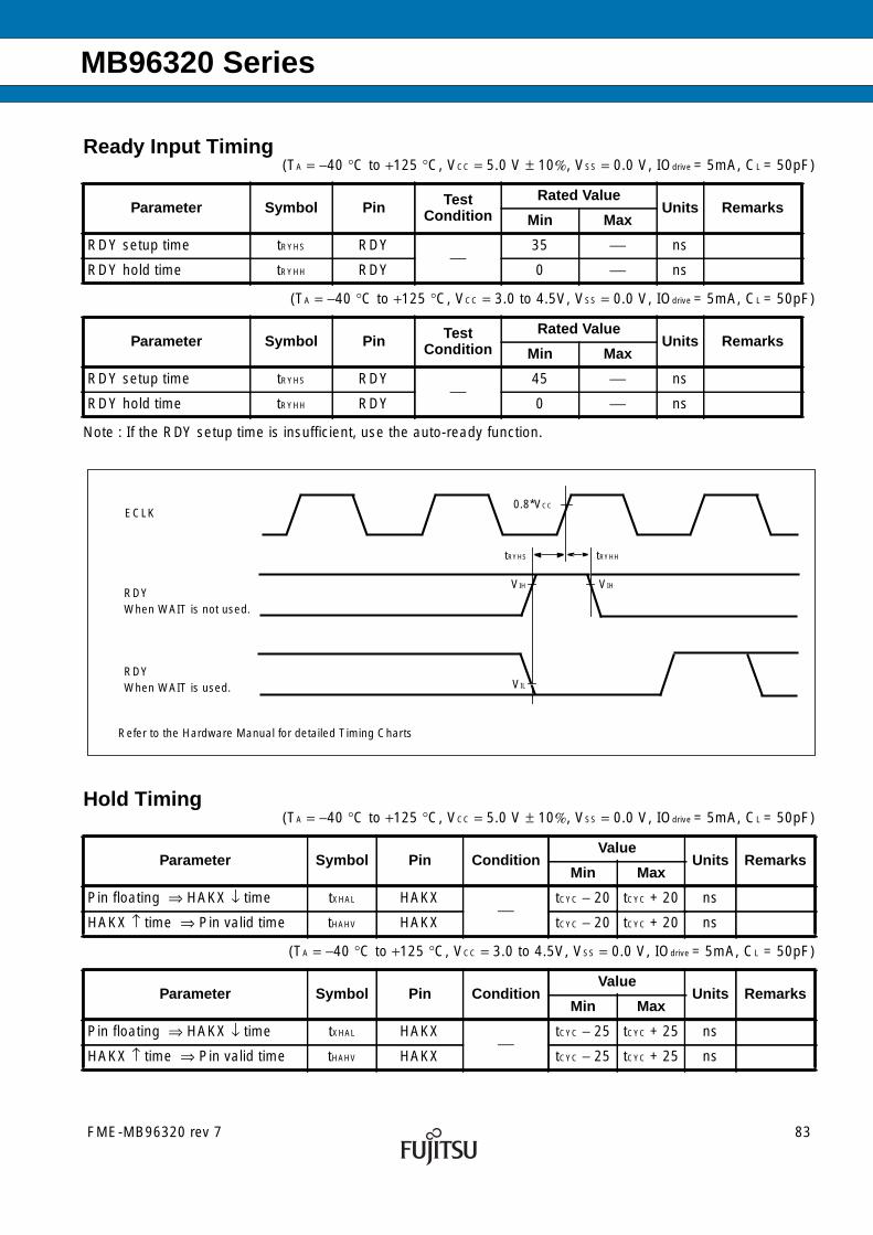
MB96320 Series
Ready Input Timing
Note : If the RDY setup time is insufficient, use the auto-ready function.
Hold Timing
(TA = −40 °C to +125 °C, VCC = 5.0 V ± 10%, VSS = 0.0 V, IOdrive = 5mA, CL = 50pF)
Parameter Symbol Pin TestCondition
Rated ValueUnits Remarks
Min Max
RDY setup time tRYHS RDY⎯
35 ⎯ ns
RDY hold time tRYHH RDY 0 ⎯ ns
(TA = −40 °C to +125 °C, VCC = 3.0 to 4.5V, VSS = 0.0 V, IOdrive = 5mA, CL = 50pF)
Parameter Symbol Pin TestCondition
Rated ValueUnits Remarks
Min Max
RDY setup time tRYHS RDY⎯
45 ⎯ ns
RDY hold time tRYHH RDY 0 ⎯ ns
(TA = −40 °C to +125 °C, VCC = 5.0 V ± 10%, VSS = 0.0 V, IOdrive = 5mA, CL = 50pF)
Parameter Symbol Pin ConditionValue
Units RemarksMin Max
Pin floating ⇒ HAKX ↓ time tXHAL HAKX⎯
tCYC − 20 tCYC + 20 ns
HAKX ↑ time ⇒ Pin valid time tHAHV HAKX tCYC − 20 tCYC + 20 ns
(TA = −40 °C to +125 °C, VCC = 3.0 to 4.5V, VSS = 0.0 V, IOdrive = 5mA, CL = 50pF)
Parameter Symbol Pin ConditionValue
Units RemarksMin Max
Pin floating ⇒ HAKX ↓ time tXHAL HAKX⎯
tCYC − 25 tCYC + 25 ns
HAKX ↑ time ⇒ Pin valid time tHAHV HAKX tCYC − 25 tCYC + 25 ns
ECLK
RDYWhen WAIT is not used.
VIH VIH
tRYHH
RDYWhen WAIT is used.
tRYHS
VIL
0.8*VCC
Refer to the Hardware Manual for detailed Timing Charts
FME-MB96320 rev 7 83

MB96320 Series
HAKX
Each pinHigh-Z
tHAHVtXHAL
0.8*VCC
0.2*VCC
0.8*VCC
0.2*VCC
Refer to the Hardware Manual for detailed Timing Charts
84 FME-MB96320 rev 7
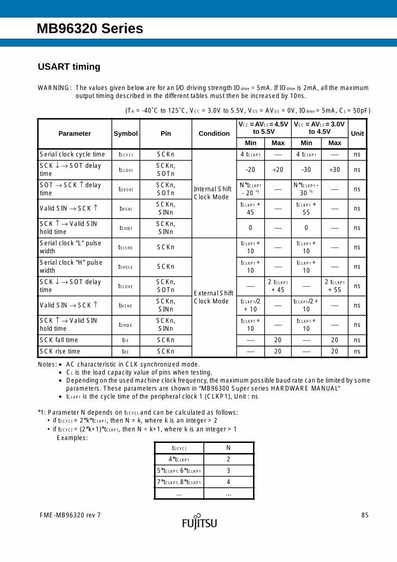
MB96320 Series
USART timing
WARNING: The values given below are for an I/O driving strength IOdrive = 5mA. If IOdrive is 2mA, all the maximumoutput timing described in the different tables must then be increased by 10ns.
Notes: • AC characteristic in CLK synchronized mode.• CL is the load capacity value of pins when testing.• Depending on the used machine clock frequency, the maximum possible baud rate can be limited by some parameters. These parameters are shown in “MB96300 Super series HARDWARE MANUAL”• tCLKP1 is the cycle time of the peripheral clock 1 (CLKP1), Unit : ns
*1: Parameter N depends on tSCYCI and can be calculated as follows:• if tSCYCI = 2*k*tCLKP1, then N = k, where k is an integer > 2• if tSCYCI = (2*k+1)*tCLKP1, then N = k+1, where k is an integer > 1
Examples:
(TA = -40˚C to 125˚C, VCC = 3.0V to 5.5V, VSS = AVSS = 0V, IOdrive = 5mA, CL = 50pF)
Parameter Symbol Pin ConditionVCC = AVCC= 4.5V
to 5.5VVCC = AVCC= 3.0V
to 4.5V UnitMin Max Min Max
Serial clock cycle time tSCYCI SCKn
Internal ShiftClock Mode
4 tCLKP1 ⎯ 4 tCLKP1 ⎯ ns
SCK ↓ → SOT delaytime
tSLOVISCKn,SOTn
-20 +20 -30 +30 ns
SOT → SCK ↑ delaytime
tOVSHISCKn,SOTn
N*tCLKP1
- 20 *1 ⎯ N*tCLKP1 -30 *1 ⎯ ns
Valid SIN → SCK ↑ tIVSHISCKn,SINn
tCLKP1 +45
⎯ tCLKP1 +55
⎯ ns
SCK ↑ → Valid SINhold time
tSHIXISCKn,SINn
0 ⎯ 0 ⎯ ns
Serial clock “L” pulsewidth
tSLSHE SCKn
External ShiftClock Mode
tCLKP1 +10
⎯ tCLKP1 +10
⎯ ns
Serial clock “H” pulsewidth
tSHSLE SCKntCLKP1 +
10⎯ tCLKP1 +
10⎯ ns
SCK ↓ → SOT delaytime
tSLOVESCKn,SOTn
⎯ 2 tCLKP1
+ 45⎯ 2 tCLKP1
+ 55ns
Valid SIN → SCK ↑ tIVSHESCKn,SINn
tCLKP1/2+ 10
⎯ tCLKP1/2 +10
⎯ ns
SCK ↑ → Valid SINhold time
tSHIXESCKn,SINn
tCLKP1 +10
⎯ tCLKP1 +10
⎯ ns
SCK fall time tFE SCKn ⎯ 20 ⎯ 20 ns
SCK rise time tRE SCKn ⎯ 20 ⎯ 20 ns
tSCYCI N
4*tCLKP1 2
5*tCLKP1, 6*tCLKP1 3
7*tCLKP1, 8*tCLKP1 4
... ...
FME-MB96320 rev 7 85

MB96320 Series
Internal Shift Clock Mode
SOT
tSLOVI
SINVIL
VIH
tIVSHI
VIL
VIH
tSHIXI
tOVSHI
SCK forESCR:SCES = 0
0.8*VCC
tSCYCI
SCK forESCR:SCES = 1
0.8*VCC 0.8*VCC
0.2*VCC
0.2*VCC
0.2*VCC
0.8*VCC
0.2*VCC
External Shift Clock Mode
tFE
VIL
VILVILVIL
SOT
tSLOVE
SINVIL
VIH
tIVSHE
VIL
VIH
tSHIXE
VIH
tRE
VIH
tSLSHE
VIL
VIH
tSHSLE
VIH
VIH
SCK forESCR:SCES = 0
SCK forESCR:SCES = 1
0.8*VCC
0.2*VCC
86 FME-MB96320 rev 7

MB96320 Series
FME-MB96320 rev 7 87
I2C Timing
*1 : For use at over 100 kHz, set the peripheral clock 1 to at least 6 MHz.
*2 : Cb = capacitance of one bus line in pF.
*3 : tCLKP1 is the cycle time of the periperal clock CLKP1.
• VOH = 0.7 * VCC
• VOL = 0.3 * VCC
• CMOS Hysteresis 0.7/0.3 input selected
(TA = -40˚C to 125˚C, VCC = AVCC = 3.0V to 5.5V,VSS = AVSS =0V)
Parameter SymbolStandard-mode Fast-mode*1
UnitMin Max Min Max
SCL clock frequency fSCL 0 100 0 400 kHz
Hold time (repeated) START conditionSDA↓→SCL↓ tHDSTA 4.0 ⎯ 0.6 ⎯ µs
“L” width of the SCL clock tLOW 4.7 ⎯ 1.3 ⎯ µs
“H” width of the SCL clock tHIGH 4.0 ⎯ 0.6 ⎯ µs
Set-up time for a repeated START conditionSCL↑→SDA↓ tSUSTA 4.7 ⎯ 0.6 ⎯ µs
Data hold timeSCL↓→SDA↓↑ tHDDAT 0 3.45 0 0.9 µs
Data set-up timeSDA↓↑→SCL↑ tSUDAT 250 ⎯ 100 ⎯ ns
Set-up time for STOP conditionSCL↑→SDA↑ tSUSTO 4.0 ⎯ 0.6 ⎯ µs
Bus free time between a STOP and STARTcondition
tBUS 4.7 ⎯ 1.3 ⎯ µs
Output fall time from 0.7*Vcc to 0.3*Vcc witha bus capacitance from 10 pF to 400 pF
tof 20 + 0.1*Cb *2 250 20 + 0.1*Cb *2 250 ns
Capacitive load for each bus line Cb ⎯ 400 ⎯ 400 pF
Pulse width of spikes which will be sup-pressed by input noise filter
tSP n/a n/a 0 1*tCLKP1*3 ns
SDA
SCL
tLOW tSUDAT tHDSTAtBUS
tHDSTA tHDDATtHIGH
tSUSTA tSUSTO
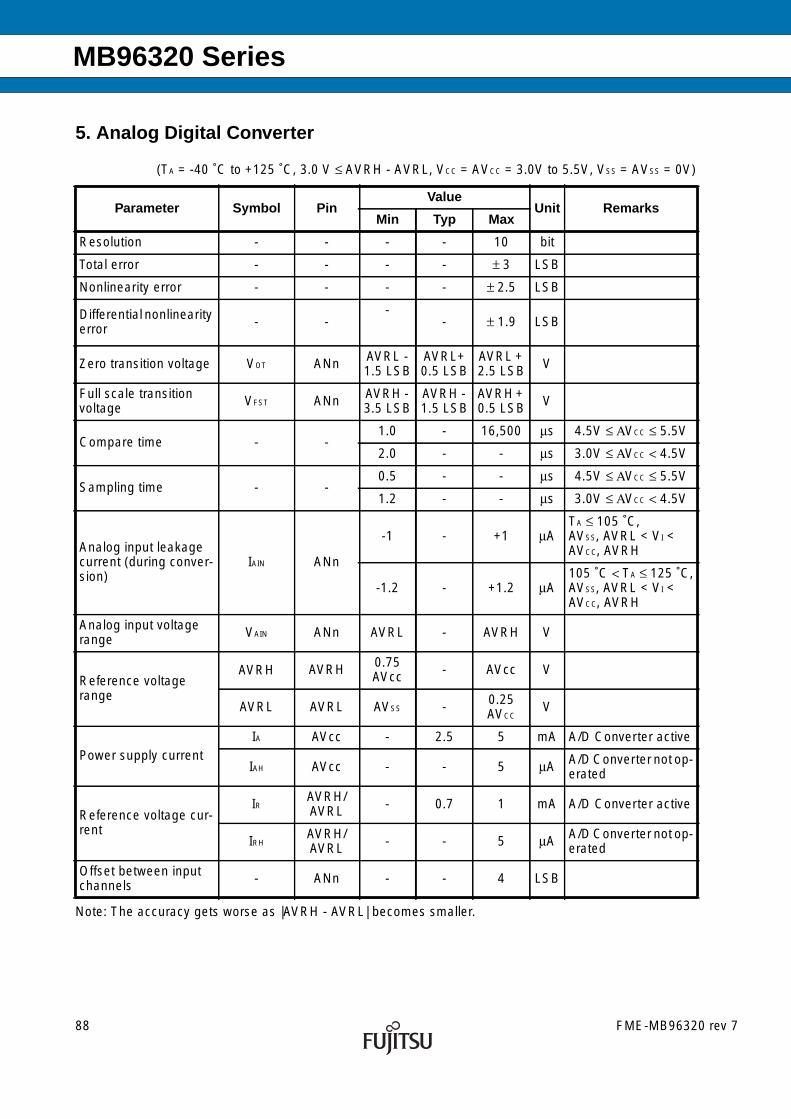
MB96320 Series
5. Analog Digital Converter
Note: The accuracy gets worse as |AVRH - AVRL| becomes smaller.
(TA = -40 ˚C to +125 ˚C, 3.0 V ≤ AVRH - AVRL, VCC = AVCC = 3.0V to 5.5V, VSS = AVSS = 0V)
Parameter Symbol PinValue
Unit RemarksMin Typ Max
Resolution - - - - 10 bit
Total error - - - - ± 3 LSB
Nonlinearity error - - - - ± 2.5 LSB
Differential nonlinearityerror - -
-- ± 1.9 LSB
Zero transition voltage VOT ANn AVRL -1.5 LSB
AVRL+0.5 LSB
AVRL +2.5 LSB V
Full scale transitionvoltage VFST ANn AVRH -
3.5 LSBAVRH -1.5 LSB
AVRH +0.5 LSB V
Compare time - -1.0 - 16,500 µs 4.5V ≤ ΑVCC ≤ 5.5V
2.0 - - µs 3.0V ≤ ΑVCC < 4.5V
Sampling time - -0.5 - - µs 4.5V ≤ ΑVCC ≤ 5.5V
1.2 - - µs 3.0V ≤ ΑVCC < 4.5V
Analog input leakagecurrent (during conver-sion)
IAIN ANn
-1 - +1 µATA ≤ 105 ˚C,AVSS, AVRL < VI <AVCC, AVRH
-1.2 - +1.2 µA105 ˚C < TA ≤ 125 ˚C,AVSS, AVRL < VI <AVCC, AVRH
Analog input voltagerange VAIN ANn AVRL - AVRH V
Reference voltagerange
AVRH AVRH 0.75AVcc - AVcc V
AVRL AVRL AVSS - 0.25AVCC
V
Power supply currentIA AVcc - 2.5 5 mA A/D Converter active
IAH AVcc - - 5 µA A/D Converter not op-erated
Reference voltage cur-rent
IR AVRH/AVRL - 0.7 1 mA A/D Converter active
IRHAVRH/AVRL - - 5 µA A/D Converter not op-
erated
Offset between inputchannels - ANn - - 4 LSB
88 FME-MB96320 rev 7
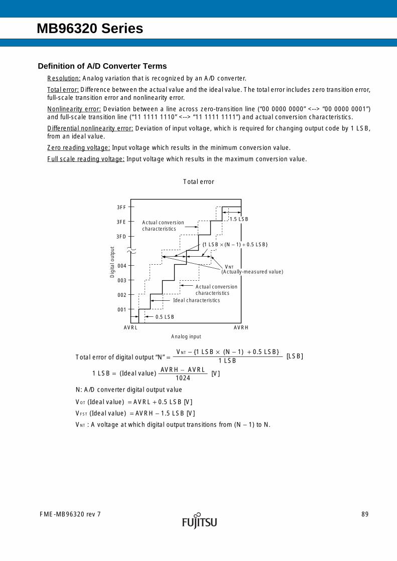
MB96320 Series
Definition of A/D Converter TermsResolution: Analog variation that is recognized by an A/D converter.
Total error: Difference between the actual value and the ideal value. The total error includes zero transition error,full-scale transition error and nonlinearity error.
Nonlinearity error: Deviation between a line across zero-transition line (“00 0000 0000” <--> “00 0000 0001”)and full-scale transition line (“11 1111 1110” <--> “11 1111 1111”) and actual conversion characteristics.
Differential nonlinearity error: Deviation of input voltage, which is required for changing output code by 1 LSB,from an ideal value.
Zero reading voltage: Input voltage which results in the minimum conversion value.
Full scale reading voltage: Input voltage which results in the maximum conversion value.
3FF
3FE
3FD
004
003
002
001
AVRL AVRH
VNT
1.5 LSB
0.5 LSB
1 LSB × (N − 1) + 0.5 LSB
Actual conversioncharacteristics
(Actually-measured value)
Actual conversioncharacteristics
Ideal characteristics
Dig
ital o
utpu
t
Analog input
Total error of digital output “N” =VNT − 1 LSB × (N − 1) + 0.5 LSB
1 LSB[LSB]
1 LSB = (Ideal value) AVRH − AVRL1024
[V]
VOT (Ideal value) = AVRL + 0.5 LSB [V]
VFST (Ideal value) = AVRH − 1.5 LSB [V]
VNT : A voltage at which digital output transitions from (N − 1) to N.
Total error
N: A/D converter digital output value
FME-MB96320 rev 7 89
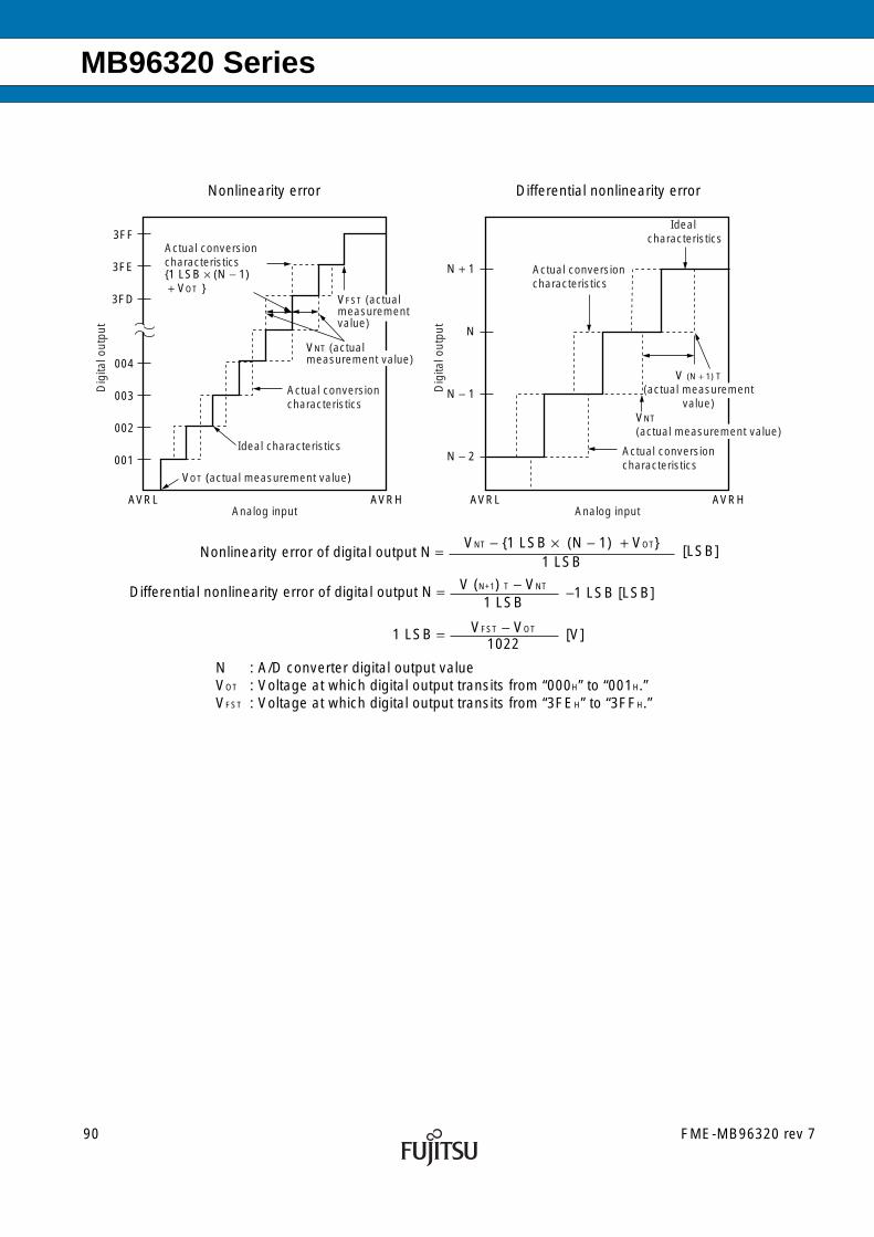
MB96320 Series
3FF
3FE
3FD
004
003
002
001
AVRL AVRH AVRL AVRH
N + 1
N
N − 1
N − 2
VOT (actual measurement value)
1 LSB × (N − 1) + VOT
Actual conversioncharacteristics
VFST (actualmeasurement value)
VNT (actualmeasurement value)
Actual conversioncharacteristics
Ideal characteristics
Actual conversioncharacteristics
Actual conversioncharacteristics
Ideal characteristics
Dig
ital o
utpu
t
Dig
ital o
utpu
t
Analog inputAnalog input
VNT
(actual measurement value)
V (N + 1) T
(actual measurementvalue)
Nonlinearity error Differential nonlinearity error
Differential nonlinearity error of digital output N =
1 LSB =
Nonlinearity error of digital output N = VNT − 1 LSB × (N − 1) + VOT1 LSB
[LSB]
V (N+1) T − VNT
1 LSB−1 LSB [LSB]
VFST − VOT
1022[V]
N : A/D converter digital output valueVOT : Voltage at which digital output transits from “000H” to “001H.”VFST : Voltage at which digital output transits from “3FEH” to “3FFH.”
90 FME-MB96320 rev 7

MB96320 Series
Accuracy and setting of the A/D Converter sampling timeIf the external impedance is too high or the sampling time too short, the analog voltage charged to the internalsample and hold capacitor is insufficient, adversely affecting the A/D conversion precision.
To satisfy the A/D conversion precision, a sufficient sampling time must be selected. The required sampling timedepends on the external driving impedance Rext, the board capacitance of the A/D converter input pin Cext andthe AVcc voltage level. The following replacement model can be used for the calculation:
The sampling time should be set to minimum “7τ“. The following approximation formula for the replacementmodel above can be used:
Tsamp [min] = 7 × (Rext × (Cext + CIN) + (Rext + RADC) × CADC)
• Do not select a sampling time below the absolute minimum permitted value(0.5µs for 4.5V ≤ AVcc ≤ 5.5V; 1.2 µs for 3.0V ≤ AVcc < 4.5V).
• If the sampling time cannot be sufficient, connect a capacitor of about 0.1 µF to the analog input pin. In thiscase the internal sampling capacitance CADC will be charged out of this external capacitance.
• A big external driving impedance also adversely affects the A/D conversion precision due to the pin inputleakage current IIL (static current before the sampling switch) or the analog input leakage current IAIN (totalleakage current of pin input and comparator during sampling). The effect of the pin input leakage current IILcannot be compensated by an external capacitor.
• The accuracy gets worse as |AVRH - AVRL| becomes smaller.
Comparator
Sampling switch
RADC
CADC
Analog
Rext
Cext
input
MCU
Source
Rext: external driving impedanceCext: capacitance of PCB at A/D converter input
RADC: resistance within MCU: 2.6kΩ (max) for 4.5V ≤ AVcc ≤ 5.5V12kΩ (max) for 3.0V ≤ AVcc < 4.5V
CADC: sampling capacitance within MCU: 10pF (max)
CIN
CIN: capacitance of MCU input pin: 15pF (max)
FME-MB96320 rev 7 91

MB96320 Series
6. Low Voltage Detector characteristics
CILCR:LVL[3:0] are the low voltage detector level select bits of the CILCR register.
For correct detection, the slope of the voltage level must satisfy .
Faster variations are regarded as noise and may not be detected.
The functional operation of the MCU is guaranteed down to the minimum low voltage detection level of“Level 0” (VDL0_MIN). The electrical characteristics however are only valid in the specified range (usually down to3.0V).
(TA = -40 ˚C to +125 ˚C, Vcc = AVcc = 3.0V - 5.5V, Vss = AVss = 0V)
Parameter SymbolValue
Unit RemarksMin Max
Stabilization time TLVDSTAB - 75 µs After power-up or changeof detection level
Level 0 VDL0 2.7 2.9 V CILCR:LVL[3:0]=”0000”
Level 1 VDL1 2.9 3.1 V CILCR:LVL[3:0]=”0001”
Level 2 VDL2 3.1 3.3 V CILCR:LVL[3:0]=”0010”
Level 3 VDL3 3.5 3.75 V CILCR:LVL[3:0]=”0011”
Level 4 VDL4 3.6 3.85 V CILCR:LVL[3:0]=”0100”
Level 5 VDL5 3.7 3.95 V CILCR:LVL[3:0]=”0101”
Level 6 VDL6 3.8 4.05 V CILCR:LVL[3:0]=”0110”
Level 7 VDL7 3.9 4.15 V CILCR:LVL[3:0]=”0111”
Level 8 VDL8 4.0 4.25 V CILCR:LVL[3:0]=”1000”
Level 9 VDL9 4.1 4.35 V CILCR:LVL[3:0]=”1001”
Level 10 VDL10 not used
Level 11 VDL11 not used
Level 12 VDL12 not used
Level 13 VDL13 not used
Level 14 VDL14 not used
Level 15 VDL15 not used
tddV 0.004Vµs
-----≤
92 FME-MB96320 rev 7
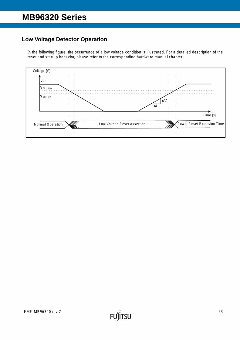
MB96320 Series
Low Voltage Detector Operation
In the following figure, the occurrence of a low voltage condition is illustrated. For a detailed description of thereset and startup behavior, please refer to the corresponding hardware manual chapter.
Voltage [V]
Time [s]
VCC
VDLx, Min
VDLx, Max
dVdt
Low Voltage Reset AssertionNormal Operation Power Reset Extension Time
FME-MB96320 rev 7 93
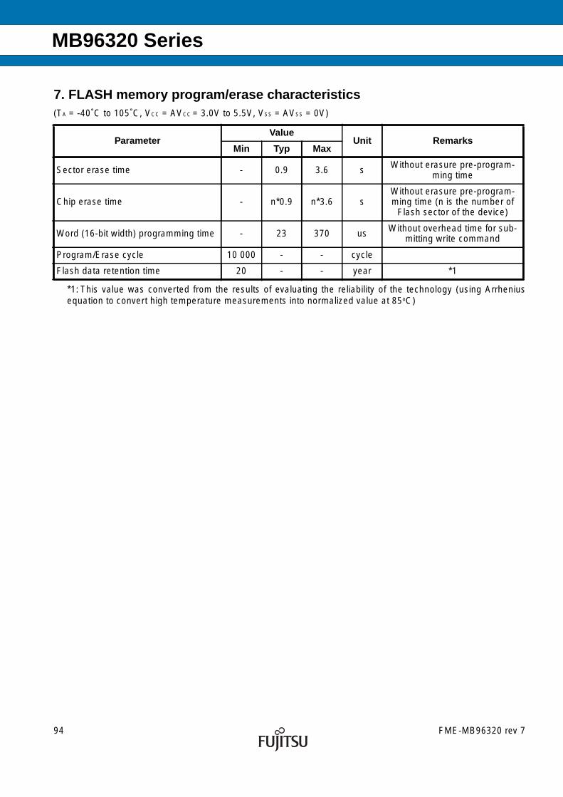
MB96320 Series
7. FLASH memory program/erase characteristics
*1: This value was converted from the results of evaluating the reliability of the technology (using Arrheniusequation to convert high temperature measurements into normalized value at 85oC)
(TA = -40˚C to 105˚C, VCC = AVCC = 3.0V to 5.5V, VSS = AVSS = 0V)
ParameterValue
Unit RemarksMin Typ Max
Sector erase time - 0.9 3.6 s Without erasure pre-program-ming time
Chip erase time - n*0.9 n*3.6 sWithout erasure pre-program-ming time (n is the number of
Flash sector of the device)
Word (16-bit width) programming time - 23 370 us Without overhead time for sub-mitting write command
Program/Erase cycle 10 000 - - cycle
Flash data retention time 20 - - year *1
94 FME-MB96320 rev 7

MB96320 Series
FME-MB96320 rev 7 95

MB96320 Series
EXAMPLE CHARACTERISTICS
1. Temperature dependency of power supply currentsThe following diagrams show the current consumption of samples with typical wafer process parameters in differ-ent operation modes.
Common condition for all operation modes:• VCC = AVCC = 5.0V• Main clock = 4MHz external clock• Sub clock = 32kHz external clock
Operation mode details:
Mode name Details
PLL Run 56 PLL Run mode current ICCPLL with the following settings:• fCLKS1 = fCLKS2 = fCLKB = fCLKP1 = 56MHz• fCLKP2 = 28MHz• Regulator in High Power Mode• Core voltage at 1.9V (VRCR:HPM[1:0] = 11B)• 2 Flash/ROM wait states (MTCRA=233AH)• RC oscillator and Sub oscillator stopped
PLL Run 48 PLL Run mode current ICCPLL with the following settings:• fCLKS1 = fCLKS2 = 96MHz• fCLKB = fCLKP1 = 48MHz• fCLKP2 = 24MHz• Regulator in High Power Mode• Core voltage at 1.9V (VRCR:HPM[1:0] = 11B)• 1 Flash/ROM wait states (MTCRA=6B09H)• RC oscillator and Sub oscillator stopped
PLL Run 24 PLL Run mode current ICCPLL with the following settings:• fCLKS1 = fCLKS2 = 48MHz• fCLKB = fCLKP1 = fCLKP2 = 24MHz• Regulator in High Power Mode• Core voltage at 1.8V (VRCR:HPM[1:0] = 10B)• 0 Flash/ROM wait states (MTCRA=2208H)• RC oscillator and Sub oscillator stopped
Main Run Main Run mode current ICCMAIN with the following settings:• fCLKS1 = fCLKS2 = fCLKB = fCLKP1 = fCLKP2 = 4MHz• Regulator in High Power Mode• Core voltage at 1.8V (VRCR:HPM[1:0] = 10B)• 1 Flash/ROM wait states (MTCRA=0239H)• PLL, RC oscillator and Sub oscillator stopped
96 FME-MB96320 rev 7

MB96320 Series
RC Run 2M RC Run mode current ICCRCH with the following settings:• RC oscillator set to 2MHz (CKFCR:RCFS = 1)• fCLKS1 = fCLKS2 = fCLKB = fCLKP1 = fCLKP2 = 2MHz• Regulator in High Power Mode• Core voltage at 1.8V (VRCR:HPM[1:0] = 10B)• 1 Flash/ROM wait states (MTCRA=0239H)• PLL, Main oscillator and Sub oscillator stopped
RC Run 100k RC Run mode current ICCRCL with the following settings:• RC oscillator set to 100kHz (CKFCR:RCFS = 0)• fCLKS1 = fCLKS2 = fCLKB = fCLKP1 = fCLKP2 = 100kHz• Regulator in Low Power Mode A (SMCR:LPMS = 1)• Core voltage at 1.8V (VRCR:LPMA[2:0] = 110B)• 1 Flash/ROM wait states (MTCRA=0239H)• PLL, Main oscillator and Sub oscillator stopped
Sub Run Sub Run mode current ICCSUB with the following settings:• fCLKS1 = fCLKS2 = fCLKB = fCLKP1 = fCLKP2 = 32kHz• Regulator in Low Power Mode A (by hardware)• Core voltage at 1.8V (VRCR:LPMA[2:0] = 110B)• 1 Flash/ROM wait states (MTCRA=0239H)• PLL, RC oscillator and Main oscillator stopped
PLL Sleep 56 PLL Sleep mode current ICCSPLL with the following settings:• fCLKS1 = fCLKS2 = fCLKP1 = 56MHz• fCLKP2 = 28MHz• Regulator in High Power Mode• Core voltage at 1.9V (VRCR:HPM[1:0] = 11B)• RC oscillator and Sub oscillator stopped
PLL Sleep 48 PLL Sleep mode current ICCSPLL with the following settings:• fCLKS1 = fCLKS2 = 96MHz• fCLKP1 = 48MHz• fCLKP2 = 24MHz• Regulator in High Power Mode• Core voltage at 1.9V (VRCR:HPM[1:0] = 11B)• RC oscillator and Sub oscillator stopped
PLL Sleep 24 PLL Sleep mode current ICCSPLL with the following settings:• fCLKS1 = fCLKS2 = 48MHz• fCLKP1 = fCLKP2 = 24MHz• Regulator in High Power Mode• Core voltage at 1.8V (VRCR:HPM[1:0] = 10B)• RC oscillator and Sub oscillator stopped
Main Sleep Main Sleep mode current ICCSMAIN with the following settings:• fCLKS1 = fCLKS2 = fCLKP1 = fCLKP2 = 4MHz• Regulator in High Power Mode• Core voltage at 1.8V (VRCR:HPM[1:0] = 10B)• PLL, RC oscillator and Sub oscillator stopped
Mode name Details
FME-MB96320 rev 7 97
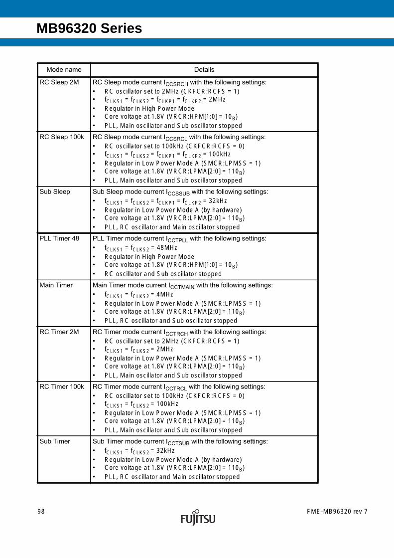
MB96320 Series
RC Sleep 2M RC Sleep mode current ICCSRCH with the following settings:• RC oscillator set to 2MHz (CKFCR:RCFS = 1)• fCLKS1 = fCLKS2 = fCLKP1 = fCLKP2 = 2MHz• Regulator in High Power Mode• Core voltage at 1.8V (VRCR:HPM[1:0] = 10B)• PLL, Main oscillator and Sub oscillator stopped
RC Sleep 100k RC Sleep mode current ICCSRCL with the following settings:• RC oscillator set to 100kHz (CKFCR:RCFS = 0)• fCLKS1 = fCLKS2 = fCLKP1 = fCLKP2 = 100kHz• Regulator in Low Power Mode A (SMCR:LPMSS = 1)• Core voltage at 1.8V (VRCR:LPMA[2:0] = 110B)• PLL, Main oscillator and Sub oscillator stopped
Sub Sleep Sub Sleep mode current ICCSSUB with the following settings:• fCLKS1 = fCLKS2 = fCLKP1 = fCLKP2 = 32kHz• Regulator in Low Power Mode A (by hardware)• Core voltage at 1.8V (VRCR:LPMA[2:0] = 110B)• PLL, RC oscillator and Main oscillator stopped
PLL Timer 48 PLL Timer mode current ICCTPLL with the following settings:• fCLKS1 = fCLKS2 = 48MHz• Regulator in High Power Mode• Core voltage at 1.8V (VRCR:HPM[1:0] = 10B)• RC oscillator and Sub oscillator stopped
Main Timer Main Timer mode current ICCTMAIN with the following settings:• fCLKS1 = fCLKS2 = 4MHz• Regulator in Low Power Mode A (SMCR:LPMSS = 1)• Core voltage at 1.8V (VRCR:LPMA[2:0] = 110B)• PLL, RC oscillator and Sub oscillator stopped
RC Timer 2M RC Timer mode current ICCTRCH with the following settings:• RC oscillator set to 2MHz (CKFCR:RCFS = 1)• fCLKS1 = fCLKS2 = 2MHz• Regulator in Low Power Mode A (SMCR:LPMSS = 1)• Core voltage at 1.8V (VRCR:LPMA[2:0] = 110B)• PLL, Main oscillator and Sub oscillator stopped
RC Timer 100k RC Timer mode current ICCTRCL with the following settings:• RC oscillator set to 100kHz (CKFCR:RCFS = 0)• fCLKS1 = fCLKS2 = 100kHz• Regulator in Low Power Mode A (SMCR:LPMSS = 1)• Core voltage at 1.8V (VRCR:LPMA[2:0] = 110B)• PLL, Main oscillator and Sub oscillator stopped
Sub Timer Sub Timer mode current ICCTSUB with the following settings:• fCLKS1 = fCLKS2 = 32kHz• Regulator in Low Power Mode A (by hardware)• Core voltage at 1.8V (VRCR:LPMA[2:0] = 110B)• PLL, RC oscillator and Main oscillator stopped
Mode name Details
98 FME-MB96320 rev 7

MB96320 Series
MB96F326 PLL Run and Sleep mode currents
Stop 1.8V Stop mode current ICCH with the following settings:• Regulator in Low Power Mode B (by hardware)• Core voltage at 1.8V (VRCR:LPMB[2:0] = 110B)
Stop 1.2V Stop mode current ICCH with the following settings:• Regulator in Low Power Mode B (by hardware)• Core voltage at 1.2V (VRCR:LPMB[2:0] = 000B)
Mode name Details
0
10
20
30
40
50
-60 -40 -20 0 20 40 60 80 100 120
Ta [˚C]
Icc[
mA
]
PLL Sleep 24
PLL Sleep 56PLL Sleep 48
PLL Run 24
PLL Run 56
PLL Run 48
FME-MB96320 rev 7 99
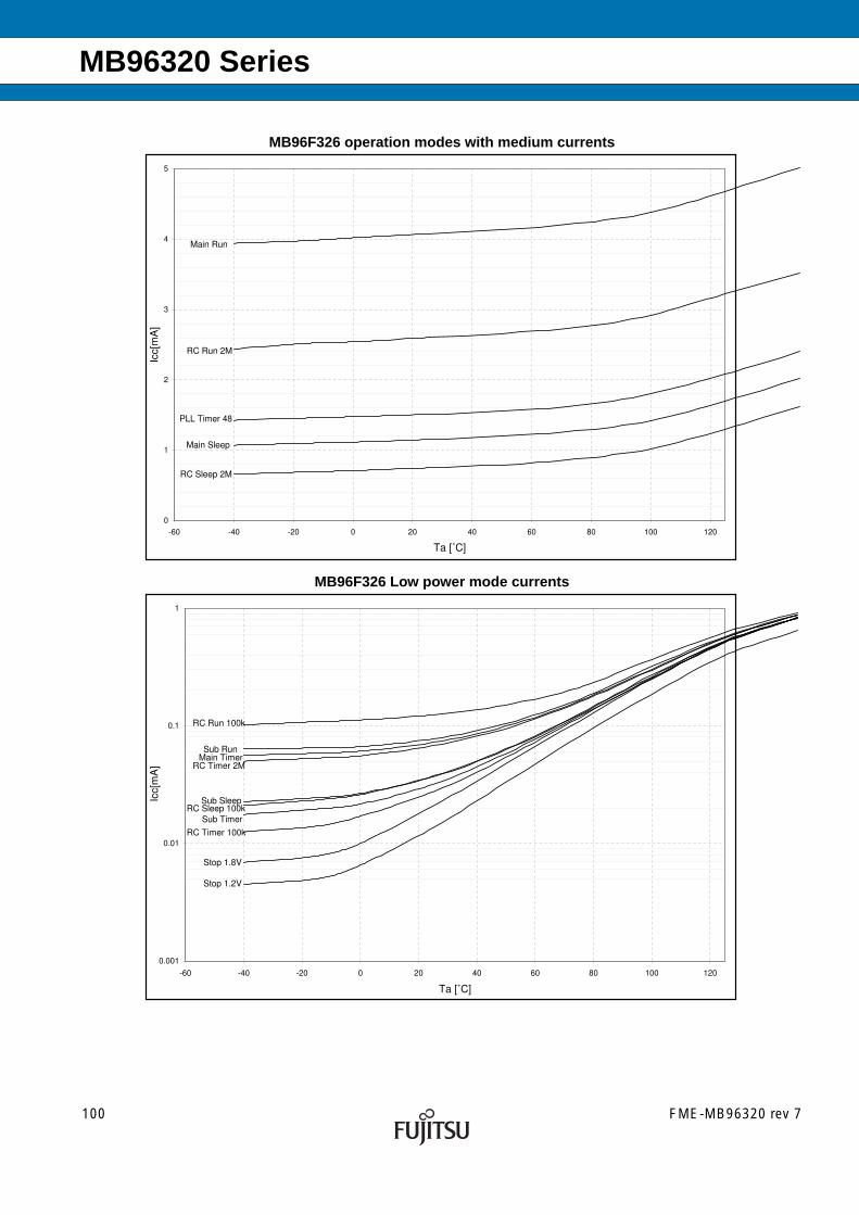
MB96320 Series
MB96F326 operation modes with medium currents
MB96F326 Low power mode currents
0
1
2
3
4
5
-60 -40 -20 0 20 40 60 80 100 120
Ta [˚C]
Icc[
mA
]
RC Sleep 2M
Main Sleep
PLL Timer 48
RC Run 2M
Main Run
0.001
0.01
0.1
1
-60 -40 -20 0 20 40 60 80 100 120
Ta [˚C]
Icc[
mA
]
Stop 1.2V
Stop 1.8V
RC Timer 100k
Sub Timer
Sub Sleep
Sub Run
RC Sleep 100k
RC Timer 2M
RC Run 100k
Main Timer
100 FME-MB96320 rev 7

MB96320 Series
2. Frequency dependency of power supply currents in PLL Run modeThe following diagrams show the current consumption of samples with typical wafer process parameters in PLLRun mode at different frequencies and Flash timing settings.
Measurement conditions:• VCC = AVCC = 5.0V• Ta = 25˚C• fCLKS1 = fCLKB or fCLKS1 = 2*fCLKB as described in diagram• fCLKS2 = fCLKS1• fCLKP1 = fCLKB• fCLKP2 = fCLKB/2• Core voltage at 1.8V (VRCR:HPM[1:0] = 10B) or 1.9V (VRCR:HPM[1:0] = 11B) as described in diagram• Main clock = 4MHz external clock• Flash memory timing settings:
• MTCRA=2128H/2208H (0 Flash wait states, fCLKS1 = 2*fCLKB)
• MTCRA=0239H/2129H (1 Flash wait state, fCLKS1 = fCLKB)
• MTCRA=4C09H/6B09H (1 Flash wait state, fCLKS1 = 2*fCLKB)
• MTCRA=233AH (2 Flash wait states, fCLKS1 = fCLKB)
• Average Flash access rate (number of read accesses to the Flash per CLKB clock cycle, no buffer hit):• 0 Flash wait states: 0.5• 1 Flash wait states: 0.33• 2 Flash wait states: 0.25
MB96F326 PLL Run mode currents
0
5
10
15
20
25
30
35
40
45
0 4 8 12 16 20 24 28 32 36 40 44 48 52 56
CLKB/CLKP1 (MHz)
ICC
PL
L (
mA
)
1 Flash wait state(CLKS1=2*CLKB, 1.9V)
1 Flash wait state(CLKS1=2*CLKB, 1.8V)
0 Flash wait states(CLKS1=2*CLKB, 1.8V)
1 Flash wait state(CLKS1=CLKB, 1.8V)
2 Flash wait states(CLKS1=CLKB, 1.8V)
2 Flash wait states(CLKS1=CLKB, 1.9V)
: Specified in "DC characteristics"
FME-MB96320 rev 7 101
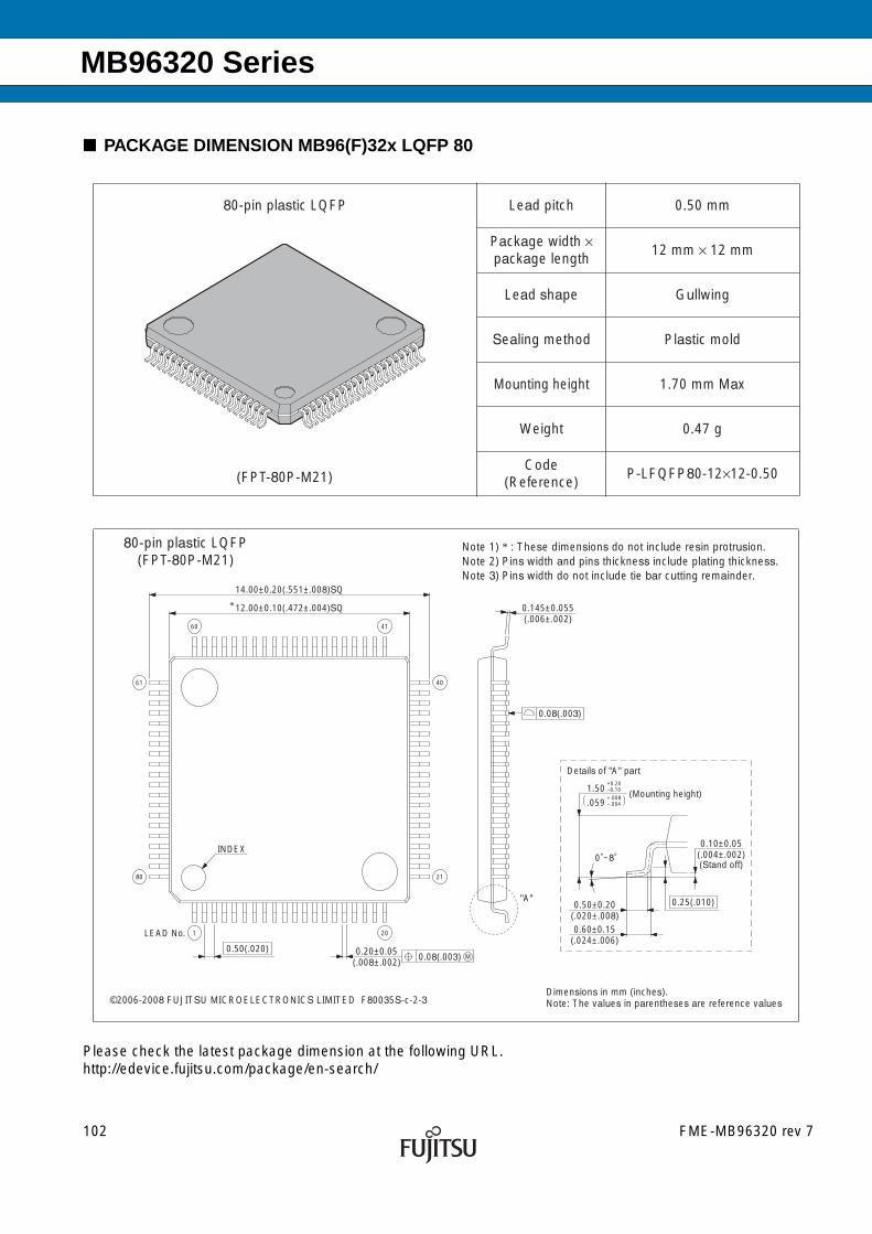
MB96320 Series
102 FME-MB96320 rev 7
PACKAGE DIMENSION MB96(F)32x LQFP 80
Please check the latest package dimension at the following URL.http://edevice.fujitsu.com/package/en-search/
80-pin plastic LQFP Lead pitch 0.50 mm
Package width ×package length
12 mm × 12 mm
Lead shape Gullwing
Sealing method Plastic mold
Mounting height 1.70 mm Max
Weight 0.47 g
Code(Reference)
P-LFQFP80-12×12-0.50
80-pin plastic LQFP(FPT-80P-M21)
(FPT-80P-M21)
C 2006 FUJITSU LIMITED F80035S-c-2-2
1 20
40
21
60 41
80
61
INDEX
12.00±0.10(.472±.004)SQ
14.00±0.20(.551±.008)SQ
0.50(.020) 0.20±0.05(.008±.002)
M0.08(.003)
0.145±0.055(.006±.002)
0.08(.003)
"A"
0˚~8˚
.059 –.004+.008
–0.10+0.20
1.50
0.50±0.20(.020±.008)0.60±0.15
(.024±.006)
0.10±0.05(.004±.002)(Stand off)
0.25(.010)
Details of "A" part
LEAD No.
(Mounting height)
*
Dimensions in mm (inches).Note: The values in parentheses are reference values©2006-2008 FUJITSU MICROELECTRONICS LIMITED F80035S-c-2-3
Note 1) * : These dimensions do not include resin protrusion.Note 2) Pins width and pins thickness include plating thickness.Note 3) Pins width do not include tie bar cutting remainder.

MB96320 Series
FME-MB96320 rev 7 103
ORDERING INFORMATION
MCU with CAN controller
MCU without CAN controller
This datasheet is also valid for the following outdated devices:MB96F326YSA, MB96F326RSA, MB96F326YWA, MB96F326RWA, MB96F326ASA, MB96F326AWA
Part number Flash/ROM SubclockPersistentLow Volt-age Reset
Package
MB96F326YSB PMC-GSE2
Flash A (288KB)
NoYes
80 pin Plastic LQFP(FPT-80P-M21)
MB96F326RSB PMC-GSE2 No
MB96F326YWB PMC-GSE2Yes
Yes
MB96F326RWB PMC-GSE2 No
MB96V300BRB-ES(for evaluation)
Emulated by ext. RAM Yes No416 pin Plastic BGA
(BGA-416P-M02)
Part number Flash/ROM SubclockPersistentLow Volt-age Reset
Package
MB96F326ASB PMC-GSE2Flash A (288KB)
No No 80 pin Plastic LQFP(FPT-80P-M21)MB96F326AWB PMC-GSE2 Yes No
MB96320 Series
REVISION HISTORY
Revision Date Modification
Prelim 1 2007-05-02 Creation
Prelim 2 2007-05-25 Electrical characteristics updates
Prelim 3 2007-11-23 Cover page: package description removed.Modification of the block diagram.Add A pin function group in pin function description.Electrical characteristics update.Add chapter on LVD and example characteristics.In ordering information: typo correction. Persistent instead of persistant.Memory map relaid out.
Prelim 4 2007-12-20 Update of the block diagram: external bus address lines, clock outputfunction pins, AVRL removed from ADC block, relayout.RAMSIZE in RAMSTART table is corrected to 12kB as in described in theproduct lineup.IO map table updatedOrdering information show now PMC packages not PQC. It displays alsothe redesigned release.IO map regeneratedMemory map and Flash configuration reworkedFew typos corrected across the document.Flash bank renaming.IO circuit drawings modified.
Prelim 5 2008-02-04 • Reload Timer RLT 6 for PPGs added• Block diagram corrected: RLT6 added, OUT10->OUT10_R, TX0/RX0
->RX2/RX2,• Pin assignment: TX3 deleted• Pin function description corrected with all existing pin types• I/O circuit type diagrams corrected• Memory map cleaned up• "Flash sector configuration" replaced by corrected "User ROM Memory
map for Flash devices"• Parallel Flash programming spec removed• IO map table regenerated:
- Port register: Naming style corrected- Memory control registers renamed (Main -> A)- addresses after 000BFFh removed
• Handling devices: AD converter items added• Absolute maximum ratings: Pd and Ta specified more precisely• Run and Sleep mode currents: more conditions added (1WS settings)• Run mode current spec in 48/24MHz mode corrected• Maximum CLKS1 frequency corrected at 1.8V• External bus timings: missing conditions added and readability improved• Ordering information updated• Typos and formatting corrected
104 FME-MB96320 rev 7
MB96320 Series
6 2009-01-09 • Format adjusted to official Fujitsu Microelectronics datasheet standard(mainly style changes and official notes and disclaimer added)
• Numbering of Electrical Characteristics subchapters automated• Devices added (MB96F326A)• I/O map: Added node about reserved registers• Serial programming interface: Note about handshaking pins improved• specified AD converter channel offset to 4LSB• package code of MB96V300 corrected in ordering information• Added voltage condition to pull-up resistance spec• Ordering information: column “Flash/ROM” added, column “Remarks” re-
moved• Official package dimension drawing with additional notes added• Empty pages removed• Handling devices: Notes added about Serial communication and about
using ceramic resonators.• Feature list and AC Characteristics: 16MHz maximum frequency is valid
for crystal oscillators. For resonators, maximum frequency depends on Q-factor
• AC characteristics: PLL phase skew spec added, CLKVCO min=64MHz• VOL3 spec improved: spec valid for 3mA load for full Vcc range• C-Pin cap spec updated: 4.7µF-10µF capacitor with tolerance permitted• “Preliminary” watermark removed
7 2010-06-22 • AD converter IAIN spec improved: 1uA valid up to 105deg, 1.2uA above105deg. Changed Unit of Vot anf Vfst from LSB to V.
• Note added that PLL phase jitter spec does not include jitter coming fromMain clock
• Removed PHDR register from IO map• Note added in DC characteristics how to select driving strength of ports• I2C AC spec updated: tof, Cb and tSP spec added, wrong footnotes and
Condition removed• I/O Circuit type: Note added for type “N” (slew rate control according to
I2C spec)• Updated Power Supply current spec in Run/Sleep/Timer/Stop modes (new
spec items in PLL Run/Sleep mode, small adjustment of most other values)• Example characteristics updated, new figures added showing dependency
of PLL Run mode current on frequency• Package dimension: Added the following sentence under the figure:
“Please confirm the latest Package dimension by following URL.http://edevice.fujitsu.com/package/en-search/”
• AD converter: Impact of input pin capacitance and external capacitanceadded to formula for calculation of the sampling time
• Added specification of RC clock stabilization time• Feature description I2C: ‘8-bit addressing’ corrected to ‘7-bit addressing’• Feature description PPG: ‘Reload timer overflow as clock input’ corrected
to ‘Reload timer underflow as clock input’• Company name updated on the cover page: Fujitsu Microelectronics Lim-
ited -> Fujitsu Semiconductor Limited
Revision Date Modification
FME-MB96320 rev 7 105

MB96320 Series FME-MB96320 rev 7

MB96320 Series
FME-MB96320 rev 7 107
MB96320 Series
FUJITSU SEMICONDUCTOR LIMITEDNomura Fudosan Shin-yokohama Bldg. 10-23, Shin-yokohama 2-Chome,Kohoku-ku Yokohama Kanagawa 222-0033, JapanTel: +81-45-415-5858http://jp.fujitsu.com/fsl/en/
For further information please contact:
North and South AmericaFUJITSU MICROELECTRONICS AMERICA, INC.1250 E. Arques Avenue, M/S 333Sunnyvale, CA 94085-5401, U.S.A.Tel: +1-408-737-5600 Fax: +1-408-737-5999http://www.fma.fujitsu.com/
EuropeFUJITSU MICROELECTRONICS EUROPE GmbHPittlerstrasse 47, 63225 Langen, GermanyTel: +49-6103-690-0 Fax: +49-6103-690-122http://emea.fujitsu.com/microelectronics/
KoreaFUJITSU MICROELECTRONICS KOREA LTD.206 Kosmo Tower Building, 1002 Daechi-Dong,Gangnam-Gu, Seoul 135-280, Republic of KoreaTel: +82-2-3484-7100 Fax: +82-2-3484-7111http://kr.fujitsu.com/fmk/
Asia PacificFUJITSU MICROELECTRONICS ASIA PTE. LTD.151 Lorong Chuan,#05-08 New Tech Park 556741 SingaporeTel : +65-6281-0770 Fax : +65-6281-0220http://www.fmal.fujitsu.com/
FUJITSU MICROELECTRONICS SHANGHAI CO., LTD.Rm. 3102, Bund Center, No.222 Yan An Road (E),Shanghai 200002, ChinaTel : +86-21-6146-3688 Fax : +86-21-6335-1605http://cn.fujitsu.com/fmc/
FUJITSU MICROELECTRONICS PACIFIC ASIA LTD.10/F., World Commerce Centre, 11 Canton Road,Tsimshatsui, Kowloon, Hong KongTel : +852-2377-0226 Fax : +852-2376-3269http://cn.fujitsu.com/fmc/en/
Specifications are subject to change without notice. For further information please contact each office.
All Rights Reserved.The contents of this document are subject to change without notice.Customers are advised to consult with sales representatives before ordering.The information, such as descriptions of function and application circuit examples, in this document are presented solely for the purposeof reference to show examples of operations and uses of FUJITSU SEMICONDUCTOR device; FUJITSU SEMICONDUCTOR doesnot warrant proper operation of the device with respect to use based on such information. When you develop equipment incorporatingthe device based on such information, you must assume any responsibility arising out of such use of the information.FUJITSU SEMICONDUCTOR assumes no liability for any damages whatsoever arising out of the use of the information.Any information in this document, including descriptions of function and schematic diagrams, shall not be construed as license of the useor exercise of any intellectual property right, such as patent right or copyright, or any other right of FUJITSU SEMICONDUCTOR or anythird party or does FUJITSU SEMICONDUCTOR warrant non-infringement of any third-party's intellectual property right or other rightby using such information. FUJITSU SEMICONDUCTOR assumes no liability for any infringement of the intellectual property rights orother rights of third parties which would result from the use of information contained herein.The products described in this document are designed, developed and manufactured as contemplated for general use, including withoutlimitation, ordinary industrial use, general office use, personal use, and household use, but are not designed, developed and manufacturedas contemplated (1) for use accompanying fatal risks or dangers that, unless extremely high safety is secured, could have a serious effectto the public, and could lead directly to death, personal injury, severe physical damage or other loss (i.e., nuclear reaction control innuclear facility, aircraft flight control, air traffic control, mass transport control, medical life support system, missile launch control inweapon system), or (2) for use requiring extremely high reliability (i.e., submersible repeater and artificial satellite).Please note that FUJITSU SEMICONDUCTOR will not be liable against you and/or any third party for any claims or damages aris-ing in connection with above-mentioned uses of the products.Any semiconductor devices have an inherent chance of failure. You must protect against injury, damage or loss from such failuresby incorporating safety design measures into your facility and equipment such as redundancy, fire protection, and prevention of over-current levels and other abnormal operating conditions.Exportation/release of any products described in this document may require necessary procedures in accordance with the regulationsof the Foreign Exchange and Foreign Trade Control Law of Japan and/or US export control laws.The company names and brand names herein are the trademarks or registered trademarks of their respective owners.
Edited: Sales Promotion Department
108 FME-MB96320 rev 7