16 lcd-tft controller (ltdc)
TRANSCRIPT

LCD-TFT controller (LTDC) RM0090
478/1745 DocID018909 Rev 15
16 LCD-TFT controller (LTDC)
This section applies only to STM32F429xx/439xx devices.
16.1 Introduction
The LCD-TFT (Liquid Crystal Display - Thin Film Transistor) display controller provides a parallel digital RGB (Red, Green, Blue) and signals for horizontal, vertical synchronisation, Pixel Clock and Data Enable as output to interface directly to a variety of LCD and TFT panels.
16.2 LTDC main features
• 24-bit RGB Parallel Pixel Output; 8 bits-per-pixel (RGB888)
• 2 display layers with dedicated FIFO (64x32-bit)
• Color Look-Up Table (CLUT) up to 256 color (256x24-bit) per layer
• Supports up to XGA (1024x768) resolution
• Programmable timings for different display panels
• Programmable Background color
• Programmable polarity for HSync, VSync and Data Enable
• Up to 8 Input color formats selectable per layer
– ARGB8888
– RGB888
– RGB565
– ARGB1555
– ARGB4444
– L8 (8-bit Luminance or CLUT)
– AL44 (4-bit alpha + 4-bit luminance)
– AL88 (8-bit alpha + 8-bit luminance)
• Pseudo-random dithering output for low bits per channel
– Dither width 2-bits for Red, Green, Blue
• Flexible blending between two layers using alpha value (per pixel or constant)
• Color Keying (transparency color)
• Programmable Window position and size
• Supports thin film transistor (TFT) color displays
• AHB master interface with burst of 16 words
• Up to 4 programmable interrupt events
DocID018909 Rev 15 479/1745
RM0090 LCD-TFT controller (LTDC)
512
16.3 LTDC functional description
16.3.1 LTDC block diagram
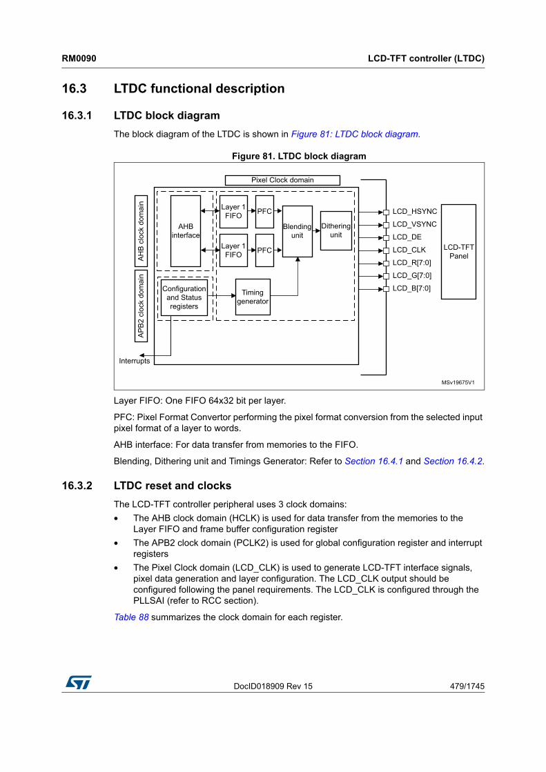
The block diagram of the LTDC is shown in Figure 81: LTDC block diagram.
Figure 81. LTDC block diagram
Layer FIFO: One FIFO 64x32 bit per layer.
PFC: Pixel Format Convertor performing the pixel format conversion from the selected input pixel format of a layer to words.
AHB interface: For data transfer from memories to the FIFO.
Blending, Dithering unit and Timings Generator: Refer to Section 16.4.1 and Section 16.4.2.
16.3.2 LTDC reset and clocks
The LCD-TFT controller peripheral uses 3 clock domains:
• The AHB clock domain (HCLK) is used for data transfer from the memories to the Layer FIFO and frame buffer configuration register
• The APB2 clock domain (PCLK2) is used for global configuration register and interrupt registers
• The Pixel Clock domain (LCD_CLK) is used to generate LCD-TFT interface signals, pixel data generation and layer configuration. The LCD_CLK output should be configured following the panel requirements. The LCD_CLK is configured through the PLLSAI (refer to RCC section).
Table 88 summarizes the clock domain for each register.

LCD-TFT controller (LTDC) RM0090
480/1745 DocID018909 Rev 15
Care must be taken when accessing the LTDC registers since the APB2 bus is stalling when the following operations are ongoing:
• Register write access and update for 6 xPCKL2 period + 5x LCD_CLK period (5x HCLK period for register on AHB clock domain)
• Register read access for 7xPCKL2 period + 5x LCD_CLK period (5x HCLK period for register on AHB clock domain).
For registers on PCLK2 clock domain, APB2 bus is stalling during the register write access for 6 xPCKL2 period and 7xPCKL2 period for read access.
The LCD controller can be reset by setting the corresponding bit in the RCC_APB2RSTR register. It resets the three clock domains.
Table 88. LTDC registers versus clock domain
LTDC registers Clock domain
LTDC_LxCR
HCLKLTDC_LxCFBAR
LTDC_LxCFBLR
LTDC_LxCFBLNR
LTDC_SRCR
PCLK2LTDC_IER
LTDC_ISR
LTDC_ICR
LTDC_SSCR
Pixel Clock (LCD_CLK)
LTDC_BPCR
LTDC_AWCR
LTDC_TWCR
LTDC_GCR
LTDC_BCCR
LTDC_LIPCR
LTDC_CPSR
LTDC_CDSR
LTDC_LxWHPCR
LTDC_LxWVPCR
LTDC_LxCKCR
LTDC_LxPFCR
LTDC_LxCACR
LTDC_LxDCCR
LTDC_LxBFCR
LTDC_LxCLUTWR
DocID018909 Rev 15 481/1745
RM0090 LCD-TFT controller (LTDC)
512
16.3.3 LCD-TFT pins and signal interface
The Table below summarizes the LTDC signal interface:
The LCD-TFT controller pins must be configured by the user application. The unused pins can be used for other purposes.
For LTDC outputs up to 24-bit (RGB888), if less than 8bpp are used to output for example RGB565 or RGB666 to interface on 16b-bit or 18-bit displays, the RGB display data lines must be connected to the MSB of the LCD-TFT controller RGB data lines. As an example, in the case of an LCD-TFT controller interfacing with a RGB565 16-bit display, the LCD display R[4:0], G[5:0] and B[4:0] data lines pins must be connected to LCD-TFT controller LCD_R[7:3], LCD_G[7:2] and LCD_B[7:3].
16.4 LTDC programmable parameters
The LCD-TFT controller provides flexible configurable parameters. It can be enabled or disabled through the LTDC_GCR register.
16.4.1 LTDC Global configuration parameters
Synchronous Timings:
Figure 82 presents the configurable timing parameters generated by the Synchronous Timings Generator block presented in the block diagram Figure 81. It generates the Horizontal and Vertical Synchronization timings panel signals, the Pixel Clock and the Data Enable signals.
Table 89. LCD-TFT pins and signal interface
LCD-TFT signals
I/O Description
LCD_CLK O Clock Output
LCD_HSYNC O Horizontal Synchronization
LCD_VSYNC O Vertical Synchronization
LCD_DE O Not Data Enable
LCD_R[7:0] O Data: 8-bit Red data
LCD_G[7:0] O Data: 8-bit Green data
LCD_B[7:0] O Data: 8-bit Blue data

LCD-TFT controller (LTDC) RM0090
482/1745 DocID018909 Rev 15
Figure 82. LCD-TFT Synchronous timings
Note: The HBP and HFP are respectively the Horizontal back porch and front porch period.
The VBP and the VFP are respectively the Vertical back porch and front porch period.
The LCD-TFT programmable synchronous timings are:
– HSYNC and VSYNC Width: Horizontal and Vertical Synchronization width configured by programming a value of HSYNC Width - 1 and VSYNC Width - 1 in the LTDC_SSCR register.
– HBP and VBP: Horizontal and Vertical Synchronization back porch width configured by programming the accumulated value HSYNC Width + HBP - 1 and the accumulated value VSYNC Width + VBP - 1 in the LTDC_BPCR register.
– Active Width and Active Height: The Active Width and Active Height are configured by programming the accumulated value HSYNC Width + HBP + Active Width - 1 and the accumulated value VSYNC Width + VBP + Active Height - 1 in the LTDC_AWCR register (only up to 1024x768 is supported).
– Total Width: The Total width is configured by programming the accumulated value HSYNC Width + HBP + Active Width + HFP - 1 in the LTDC_TWCR register. The HFP is the Horizontal front porch period.
– Total Height: The Total Height is configured by programming the accumulated value VSYNC Height + VBP + Active Height + VFP - 1 in the LTDC_TWCR register. The VFP is the Vertical front porch period.
Note: When the LTDC is enabled, the timings generated start with X/Y=0/0 position as the first horizontal synchronization pixel in the vertical synchronization area and following the back porch, active data display area and the front porch.

DocID018909 Rev 15 483/1745
RM0090 LCD-TFT controller (LTDC)
512
When the LTDC is disabled, the timing generator block is reset to X=Total Width - 1, Y=Total Height - 1 and held the last pixel before the vertical synchronization phase and the FIFO are flushed. Therefore only blanking data is output continuously.
Example of Synchronous timings configuration
TFT-LCD timings (should be extracted from Panel datasheet):
• Horizontal and Vertical Synchronization width: 0x8 pixels and 0x4 lines
• Horizontal and Vertical back porch: 0x7 pixels and 0x2 lines
• Active Width and Active Height: 0x280 pixels, 0x1E0 lines (640x480)
• Horizontal front porch: 0x6 pixels
• Vertical front porch: 0x2 lines
The programmed values in the LTDC Timings registers will be:
• LTDC_SSCR register: to be programmed to 0x00070003. (HSW[11:0] is 0x7 and VSH[10:0] is 0x3)
• LTDC_BPCR register: to be programmed to 0x000E0005. (AHBP[11:0] is 0xE(0x8 + 0x6) and AVBP[10:0] is 0x5(0x4 + 0x1))
• LTDC_AWCR register: to be programmed to 0x028E01E5. (AAW[11:0] is 0x28E(0x8 +0x7 +0x27F) and AAH[10:0] is 0x1E5(0x4 +0x2 + 0x1DF)
• LTDC_TWCR register: to be programmed to 0x00000294. (TOTALW[11:0] is 0x294(0x8 +0x7 +0x280 + 0x5)
• LTDC_THCR register: to be programmed to 0x000001E7. (TOTALH[10:0] is 0x1E7(0x4 +0x2 + 0x1E0 + 1)
Programmable polarity
The Horizontal and Vertical Synchronization, Data Enable and Pixel Clock output signals polarity can be programmed to active high or active low through the LTDC_GCR register.
Background Color
A constant background color (RGB888) can programmed through the LTDC_BCCR register. It is used for blending with the bottom layer.
Dithering
The Dithering pseudo-random technique using an LFSR is used to add a small random value (threshold) to each pixel color channel (R, G or B) value, thus rounding up the MSB in some cases when displaying a 24-bit data on 18-bit display. Thus the Dithering technique is used to round data which is different from one frame to the other.
The Dither pseudo-random technique is the same as comparing LSBs against a threshold value and adding a 1 to the MSB part only, if the LSB part is >= the threshold. The LSBs are typically dropped once dithering was applied.
The width of the added pseudo-random value is 2 bits for each color channel; 2 bits for Red, 2 bits for Green and 2 bits for Blue.
Once the LCD-TFT controller is enabled, the LFSR starts running with the first active pixel and it is kept running even during blanking periods and when dithering is switched off. If the LTDC is disabled, the LFSR is reset.
The Dithering can be switched On and Off on the fly through the LTDC_GCR register.
LCD-TFT controller (LTDC) RM0090
484/1745 DocID018909 Rev 15
Reload Shadow registers
Some configuration registers are shadowed. The shadow registers values can be reloaded immediately to the active registers when writing to these registers or at the beginning of the vertical blanking period following the configuration in the LTDC_SRCR register. If the immediate reload configuration is selected, the reload should be only activated when all new registers have been written.
The shadow registers should not be modified again before the reload has been done. Reading from the shadow registers returns the actual active value. The new written value can only be read after the reload has taken place.
A register reload interrupt can be generated if enabled in the LTDC_IER register.
The shadowed registers are all the Layer 1 and Layer 2 registers except the LTDC_LxCLUTWR register.
Interrupt generation event
Refer to Section 16.5: LTDC interrupts for interrupt configuration.
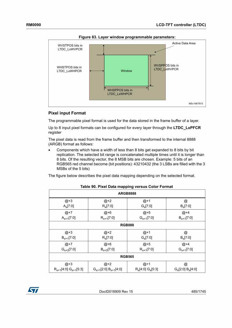
16.4.2 Layer programmable parameters
Up to two layers can be enabled, disabled and configured separately. The layer display order is fixed and it is bottom up. If two layers are enabled, the Layer2 is the top displayed window.
Windowing
Every layer can be positioned and resized and it must be inside the Active Display area.
The window position and size are configured through the top-left and bottom-right X/Y positions and the Internal timing generator which includes the synchronous, back porch size and the active data area. Refer to LTDC_LxWHPCR and LTDC_WVPCR registers.
The programmable layer position and size defines the first/last visible pixel of a line and the first/last visible line in the window. It allows to display either the full image frame or only a part of the image frame. Refer to Figure 83
• The first and the last visible pixel in the layer are set by configuring the WHSTPOS[11:0] and WHSPPOS[11:0] in the LTDC_LxWHPCR register.
• The first and the last visible lines in the layer are set by configuring the WVSTPOS[10:0] and WVSPPOS[10:0] in the LTDC_LxWVPCR register.
DocID018909 Rev 15 485/1745
RM0090 LCD-TFT controller (LTDC)
512
Figure 83. Layer window programmable parameters:
Pixel input Format
The programmable pixel format is used for the data stored in the frame buffer of a layer.
Up to 8 input pixel formats can be configured for every layer through the LTDC_LxPFCR register
The pixel data is read from the frame buffer and then transformed to the internal 8888 (ARGB) format as follows:
• Components which have a width of less than 8 bits get expanded to 8 bits by bit replication. The selected bit range is concatenated multiple times until it is longer than 8 bits. Of the resulting vector, the 8 MSB bits are chosen. Example: 5 bits of an RGB565 red channel become (bit positions): 43210432 (the 3 LSBs are filled with the 3 MSBs of the 5 bits)
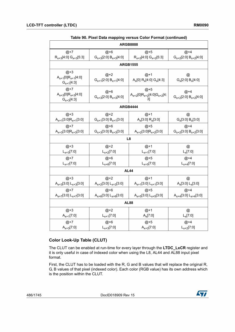
The figure below describes the pixel data mapping depending on the selected format.
Table 90. Pixel Data mapping versus Color Format
ARGB8888
@+3
Ax[7:0]
@+2
Rx[7:0]
@+1
Gx[7:0]
@
Bx[7:0]
@+7
Ax+1[7:0]
@+6
Rx+1[7:0]
@+5
Gx+1[7:0]
@+4
Bx+1[7:0]
RGB888
@+3
Bx+1[7:0]
@+2
Rx[7:0]
@+1
Gx[7:0]
@
Bx[7:0]
@+7
Gx+2[7:0]
@+6
Bx+2[7:0]
@+5
Rx+1[7:0]
@+4
Gx+1[7:0]
RGB565
@+3
Rx+1[4:0] Gx+1[5:3]
@+2
Gx+1[2:0] Bx+1[4:0]
@+1
Rx[4:0] Gx[5:3]
@
Gx[2:0] Bx[4:0]
LCD-TFT controller (LTDC) RM0090
486/1745 DocID018909 Rev 15
Color Look-Up Table (CLUT)
The CLUT can be enabled at run-time for every layer through the LTDC_LxCR register and it is only useful in case of indexed color when using the L8, AL44 and AL88 input pixel format.
First, the CLUT has to be loaded with the R, G and B values that will replace the original R, G, B values of that pixel (indexed color). Each color (RGB value) has its own address which is the position within the CLUT.
@+7
Rx+3[4:0] Gx+3[5:3]
@+6
Gx+3[2:0] Bx+3[4:0]
@+5
Rx+2[4:0] Gx+2[5:3]
@+4
Gx+2[2:0] Bx+2[4:0]
ARGB1555
@+3
Ax+1[0]Rx+1[4:0]
Gx+1[4:3]
@+2
Gx+1[2:0] Bx+1[4:0]
@+1
Ax[0] Rx[4:0] Gx[4:3]
@
Gx[2:0] Bx[4:0]
@+7
Ax+3[0]Rx+3[4:0]
Gx+3[4:3]
@+6
Gx+3[2:0] Bx+3[4:0]
@+5
Ax+2[0]Rx+2[4:0]Gx+2[4:3]
@+4
Gx+2[2:0] Bx+2[4:0]
ARGB4444
@+3
Ax+1[3:0]Rx+1[3:0]
@+2
Gx+1[3:0] Bx+1[3:0]
@+1
Ax[3:0] Rx[3:0]
@
Gx[3:0] Bx[3:0]
@+7
Ax+3[3:0]Rx+3[3:0]
@+6
Gx+3[3:0] Bx+3[3:0]
@+5
Ax+2[3:0]Rx+2[3:0]
@+4
Gx+2[3:0] Bx+2[3:0]
L8
@+3
Lx+3[7:0]
@+2
Lx+2[7:0]
@+1
Lx+1[7:0]
@
Lx[7:0]
@+7
Lx+7[7:0]
@+6
Lx+6[7:0]
@+5
Lx+5[7:0]
@+4
Lx+4[7:0]
AL44
@+3
Ax+3[3:0] Lx+3[3:0]
@+2
Ax+2[3:0] Lx+2[3:0]
@+1
Ax+1[3:0] Lx+1[3:0]
@
Ax[3:0] Lx[3:0]
@+7
Ax+7[3:0] Lx+7[3:0]
@+6
Ax+6[3:0] Lx+6[3:0]
@+5
Ax+5[3:0] Lx+5[3:0]
@+4
Ax+4[3:0] Lx+4[3:0]
AL88
@+3
Ax+1[7:0]
@+2
Lx+1[7:0]
@+1
Ax[7:0]
@
Lx[7:0]
@+7
Ax+3[7:0]
@+6
Lx+3[7:0]
@+5
Ax+2[7:0]
@+4
Lx+2[7:0]
Table 90. Pixel Data mapping versus Color Format (continued)
ARGB8888

DocID018909 Rev 15 487/1745
RM0090 LCD-TFT controller (LTDC)
512
The R, G and B values and their own respective address are programmed through the LTDC_LxCLUTWR register.
• In case of L8 and AL88 input pixel format, the CLUT has to be loaded by 256 colors. The address of each color is configured in the CLUTADD bits in the LTDC_LxCLUTWR register.
• In case of AL44 input pixel format, the CLUT has to be only loaded by 16 colors. The address of each color must be filled by replicating the 4-bit L channel to 8-bit as follows:
– L0 (indexed color 0), at address 0x00
– L1, at address 0x11
– L2, at address 0x22
– .....
– L15, at address 0xFF
Color Frame Buffer Address
Every Layer has a start address for the color frame buffer configured through the LTDC_LxCFBAR register.
When a layer is enabled, the data is fetched from the Color Frame Buffer.
Color Frame Buffer Length
Every layer has a total line length setting for the color frame buffer in bytes and a number of lines in the frame buffer configurable in the LTDC_LxCFBLR and LTDC_LxCFBLNR register respectively.
The line length and the number of lines settings are used to stop the prefetching of data to the layer FIFO at the end of the frame buffer.
• If it is set to less bytes than required, a FIFO underrun interrupt is generated if it has been previously enabled.
• If it is set to more bytes than actually required, the useless data read from the FIFO is discarded. The useless data is not displayed.
Color Frame Buffer Pitch
Every layer has a configurable pitch for the color frame buffer, which is the distance between the start of one line and the beginning of the next line in bytes. It is configured through the LTDC_LxCFBLR register.
Layer Blending
The blending is always active and the two layers can be blended following the blending factors configured through the LTDC_LxBFCR register.
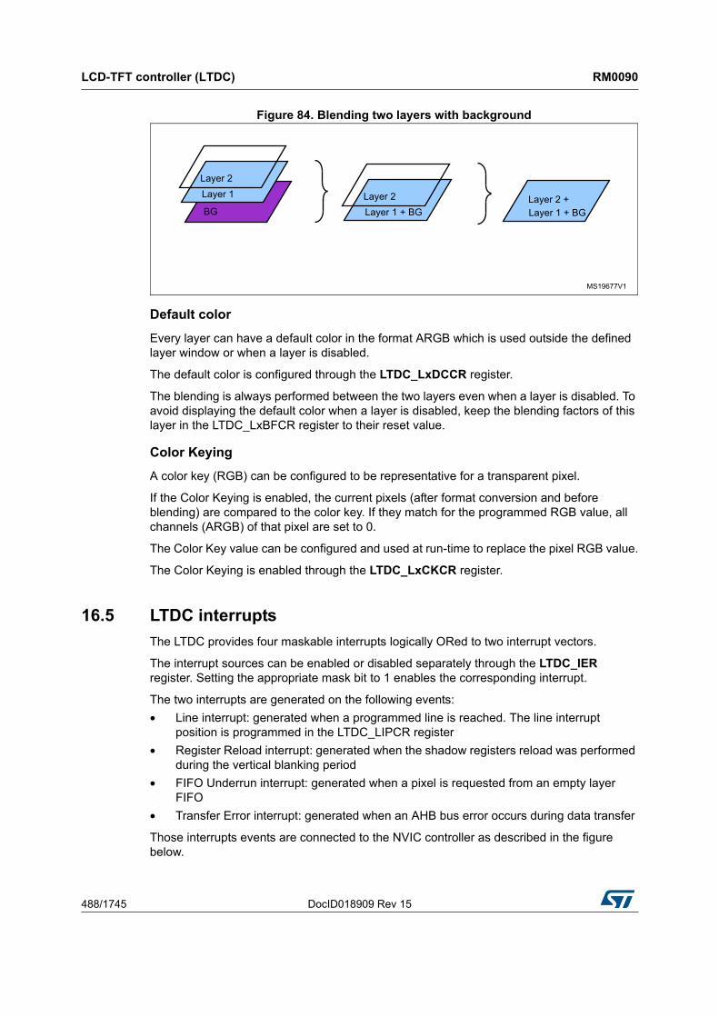
The blending order is fixed and it is bottom up. If two layers are enabled, first the Layer1 is blended with the Background color, then the Layer2 is blended with the result of blended color of Layer1 and the background. Refer to Figure 84.
LCD-TFT controller (LTDC) RM0090
488/1745 DocID018909 Rev 15
Figure 84. Blending two layers with background
Default color
Every layer can have a default color in the format ARGB which is used outside the defined layer window or when a layer is disabled.
The default color is configured through the LTDC_LxDCCR register.
The blending is always performed between the two layers even when a layer is disabled. To avoid displaying the default color when a layer is disabled, keep the blending factors of this layer in the LTDC_LxBFCR register to their reset value.
Color Keying
A color key (RGB) can be configured to be representative for a transparent pixel.
If the Color Keying is enabled, the current pixels (after format conversion and before blending) are compared to the color key. If they match for the programmed RGB value, all channels (ARGB) of that pixel are set to 0.
The Color Key value can be configured and used at run-time to replace the pixel RGB value.
The Color Keying is enabled through the LTDC_LxCKCR register.
16.5 LTDC interrupts
The LTDC provides four maskable interrupts logically ORed to two interrupt vectors.
The interrupt sources can be enabled or disabled separately through the LTDC_IER register. Setting the appropriate mask bit to 1 enables the corresponding interrupt.
The two interrupts are generated on the following events:
• Line interrupt: generated when a programmed line is reached. The line interrupt position is programmed in the LTDC_LIPCR register
• Register Reload interrupt: generated when the shadow registers reload was performed during the vertical blanking period
• FIFO Underrun interrupt: generated when a pixel is requested from an empty layer FIFO
• Transfer Error interrupt: generated when an AHB bus error occurs during data transfer
Those interrupts events are connected to the NVIC controller as described in the figure below.
DocID018909 Rev 15 489/1745
RM0090 LCD-TFT controller (LTDC)
512
Figure 85. Interrupt events
Table 91. LTDC interrupt requests
Interrupt event Event flag Enable Control bit
Line LIF LIE
Register Reload RRIF RRIEN
FIFO Underrun FUDERRIF FUDERRIE
Transfer Error TERRIF TERRIE

LCD-TFT controller (LTDC) RM0090
490/1745 DocID018909 Rev 15
16.6 LTDC programming procedure
• Enable the LTDC clock in the RCC register
• Configure the required Pixel clock following the panel datasheet
• Configure the Synchronous timings: VSYNC, HSYNC, Vertical and Horizontal back porch, active data area and the front porch timings following the panel datasheet as described in the Section 16.4.1: LTDC Global configuration parameters
• Configure the synchronous signals and clock polarity in the LTDC_GCR register
• If needed, configure the background color in the LTDC_BCCR register
• Configure the needed interrupts in the LTDC_IER and LTDC_LIPCR register
• Configure the Layer1/2 parameters by programming:
– The Layer window horizontal and vertical position in the LTDC_LxWHPCR and LTDC_WVPCR registers. The layer window must be in the active data area.
– The pixel input format in the LTDC_LxPFCR register
– The color frame buffer start address in the LTDC_LxCFBAR register
– The line length and pitch of the color frame buffer in the LTDC_LxCFBLR register
– The number of lines of the color frame buffer in the LTDC_LxCFBLNR register
– if needed, load the CLUT with the RGB values and its address in the LTDC_LxCLUTWR register
– If needed, configure the default color and the blending factors respectively in the LTDC_LxDCCR and LTDC_LxBFCR registers
• Enable Layer1/2 and if needed the CLUT in the LTDC_LxCR register
• If needed, dithering and color keying can be enabled respectively in the LTDC_GCR and LTDC_LxCKCR registers. It can be also enabled on the fly.
• Reload the shadow registers to active register through the LTDC_SRCR register.
• Enable the LCD-TFT controller in the LTDC_GCR register.
• All layer parameters can be modified on the fly except the CLUT. The new configuration has to be either reloaded immediately or during vertical blanking period by configuring the LTDC_SRCR register.
Note: All layer’s registers are shadowed. Once a register is written, it should not be modified again before the reload has been done. Thus, a new write to the same register will override the previous configuration if not yet reloaded.
DocID018909 Rev 15 491/1745
RM0090 LCD-TFT controller (LTDC)
512
16.7 LTDC registers
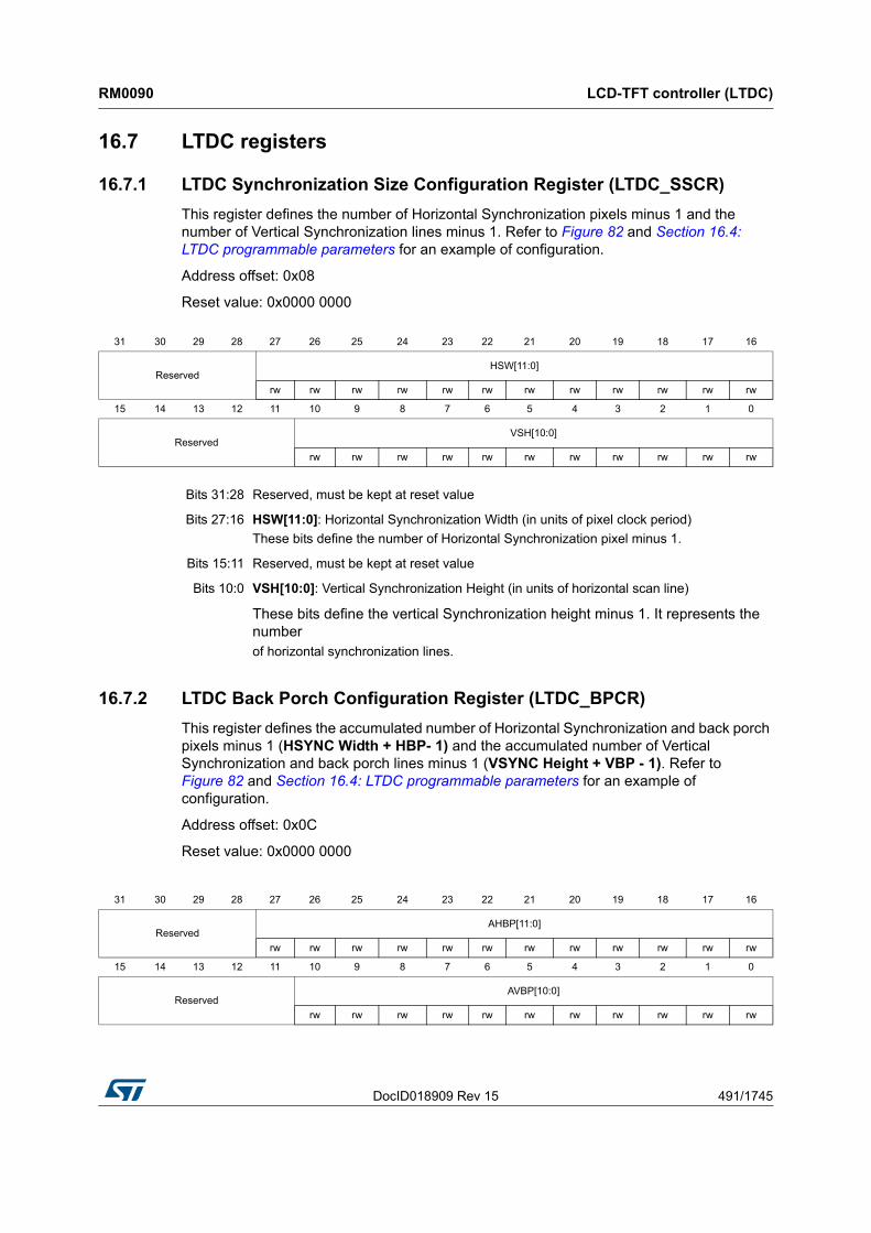
16.7.1 LTDC Synchronization Size Configuration Register (LTDC_SSCR)
This register defines the number of Horizontal Synchronization pixels minus 1 and the number of Vertical Synchronization lines minus 1. Refer to Figure 82 and Section 16.4: LTDC programmable parameters for an example of configuration.
Address offset: 0x08
Reset value: 0x0000 0000
16.7.2 LTDC Back Porch Configuration Register (LTDC_BPCR)
This register defines the accumulated number of Horizontal Synchronization and back porch pixels minus 1 (HSYNC Width + HBP- 1) and the accumulated number of Vertical Synchronization and back porch lines minus 1 (VSYNC Height + VBP - 1). Refer to Figure 82 and Section 16.4: LTDC programmable parameters for an example of configuration.
Address offset: 0x0C
Reset value: 0x0000 0000
31 30 29 28 27 26 25 24 23 22 21 20 19 18 17 16
ReservedHSW[11:0]
rw rw rw rw rw rw rw rw rw rw rw rw
15 14 13 12 11 10 9 8 7 6 5 4 3 2 1 0
ReservedVSH[10:0]
rw rw rw rw rw rw rw rw rw rw rw
Bits 31:28 Reserved, must be kept at reset value
Bits 27:16 HSW[11:0]: Horizontal Synchronization Width (in units of pixel clock period)
These bits define the number of Horizontal Synchronization pixel minus 1.
Bits 15:11 Reserved, must be kept at reset value
Bits 10:0 VSH[10:0]: Vertical Synchronization Height (in units of horizontal scan line)
These bits define the vertical Synchronization height minus 1. It represents the numberof horizontal synchronization lines.
31 30 29 28 27 26 25 24 23 22 21 20 19 18 17 16
ReservedAHBP[11:0]
rw rw rw rw rw rw rw rw rw rw rw rw
15 14 13 12 11 10 9 8 7 6 5 4 3 2 1 0
ReservedAVBP[10:0]
rw rw rw rw rw rw rw rw rw rw rw
LCD-TFT controller (LTDC) RM0090
492/1745 DocID018909 Rev 15
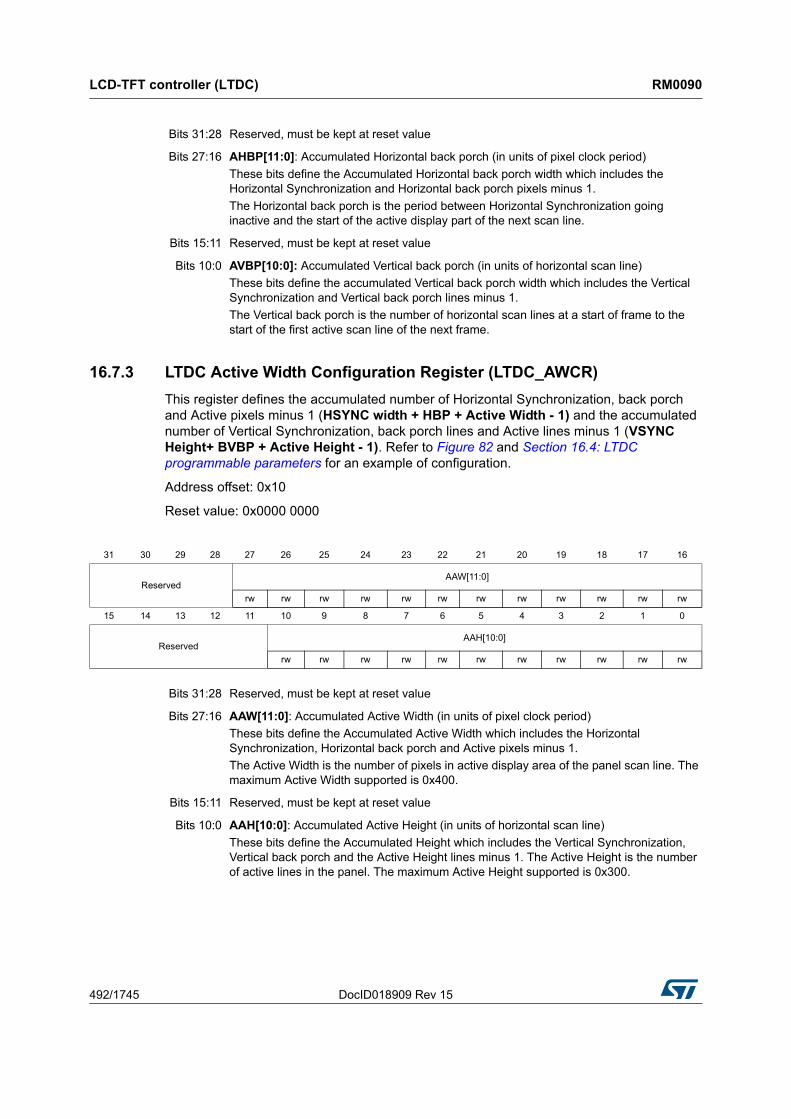
16.7.3 LTDC Active Width Configuration Register (LTDC_AWCR)
This register defines the accumulated number of Horizontal Synchronization, back porch and Active pixels minus 1 (HSYNC width + HBP + Active Width - 1) and the accumulated number of Vertical Synchronization, back porch lines and Active lines minus 1 (VSYNC Height+ BVBP + Active Height - 1). Refer to Figure 82 and Section 16.4: LTDC programmable parameters for an example of configuration.
Address offset: 0x10
Reset value: 0x0000 0000
Bits 31:28 Reserved, must be kept at reset value
Bits 27:16 AHBP[11:0]: Accumulated Horizontal back porch (in units of pixel clock period)
These bits define the Accumulated Horizontal back porch width which includes the Horizontal Synchronization and Horizontal back porch pixels minus 1.
The Horizontal back porch is the period between Horizontal Synchronization going inactive and the start of the active display part of the next scan line.
Bits 15:11 Reserved, must be kept at reset value
Bits 10:0 AVBP[10:0]: Accumulated Vertical back porch (in units of horizontal scan line)
These bits define the accumulated Vertical back porch width which includes the Vertical Synchronization and Vertical back porch lines minus 1.
The Vertical back porch is the number of horizontal scan lines at a start of frame to the start of the first active scan line of the next frame.
31 30 29 28 27 26 25 24 23 22 21 20 19 18 17 16
ReservedAAW[11:0]
rw rw rw rw rw rw rw rw rw rw rw rw
15 14 13 12 11 10 9 8 7 6 5 4 3 2 1 0
ReservedAAH[10:0]
rw rw rw rw rw rw rw rw rw rw rw
Bits 31:28 Reserved, must be kept at reset value
Bits 27:16 AAW[11:0]: Accumulated Active Width (in units of pixel clock period)
These bits define the Accumulated Active Width which includes the Horizontal Synchronization, Horizontal back porch and Active pixels minus 1.
The Active Width is the number of pixels in active display area of the panel scan line. The maximum Active Width supported is 0x400.
Bits 15:11 Reserved, must be kept at reset value
Bits 10:0 AAH[10:0]: Accumulated Active Height (in units of horizontal scan line)
These bits define the Accumulated Height which includes the Vertical Synchronization, Vertical back porch and the Active Height lines minus 1. The Active Height is the number of active lines in the panel. The maximum Active Height supported is 0x300.
DocID018909 Rev 15 493/1745
RM0090 LCD-TFT controller (LTDC)
512
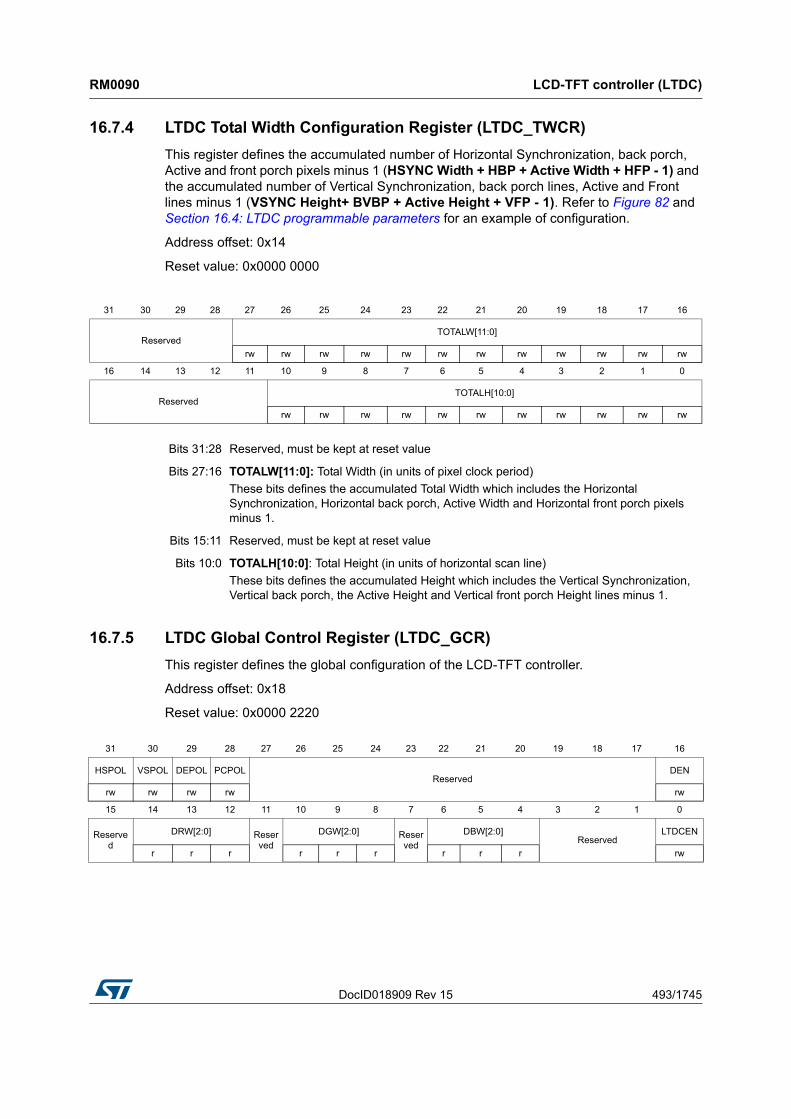
16.7.4 LTDC Total Width Configuration Register (LTDC_TWCR)
This register defines the accumulated number of Horizontal Synchronization, back porch, Active and front porch pixels minus 1 (HSYNC Width + HBP + Active Width + HFP - 1) and the accumulated number of Vertical Synchronization, back porch lines, Active and Front lines minus 1 (VSYNC Height+ BVBP + Active Height + VFP - 1). Refer to Figure 82 and Section 16.4: LTDC programmable parameters for an example of configuration.
Address offset: 0x14
Reset value: 0x0000 0000
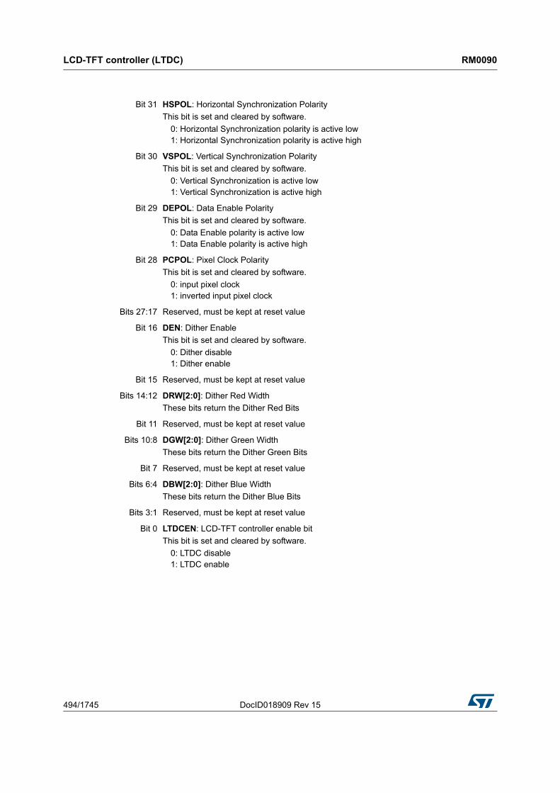
16.7.5 LTDC Global Control Register (LTDC_GCR)
This register defines the global configuration of the LCD-TFT controller.
Address offset: 0x18
Reset value: 0x0000 2220
31 30 29 28 27 26 25 24 23 22 21 20 19 18 17 16
ReservedTOTALW[11:0]
rw rw rw rw rw rw rw rw rw rw rw rw
16 14 13 12 11 10 9 8 7 6 5 4 3 2 1 0
ReservedTOTALH[10:0]
rw rw rw rw rw rw rw rw rw rw rw
Bits 31:28 Reserved, must be kept at reset value
Bits 27:16 TOTALW[11:0]: Total Width (in units of pixel clock period)
These bits defines the accumulated Total Width which includes the Horizontal Synchronization, Horizontal back porch, Active Width and Horizontal front porch pixels minus 1.
Bits 15:11 Reserved, must be kept at reset value
Bits 10:0 TOTALH[10:0]: Total Height (in units of horizontal scan line)
These bits defines the accumulated Height which includes the Vertical Synchronization, Vertical back porch, the Active Height and Vertical front porch Height lines minus 1.
31 30 29 28 27 26 25 24 23 22 21 20 19 18 17 16
HSPOL VSPOL DEPOL PCPOLReserved
DEN
rw rw rw rw rw
15 14 13 12 11 10 9 8 7 6 5 4 3 2 1 0
Reserved
DRW[2:0] Reserved
DGW[2:0] Reserved
DBW[2:0]Reserved
LTDCEN
r r r r r r r r r rw
LCD-TFT controller (LTDC) RM0090
494/1745 DocID018909 Rev 15
Bit 31 HSPOL: Horizontal Synchronization Polarity
This bit is set and cleared by software.
0: Horizontal Synchronization polarity is active low1: Horizontal Synchronization polarity is active high
Bit 30 VSPOL: Vertical Synchronization Polarity
This bit is set and cleared by software.
0: Vertical Synchronization is active low 1: Vertical Synchronization is active high
Bit 29 DEPOL: Data Enable Polarity
This bit is set and cleared by software.
0: Data Enable polarity is active low1: Data Enable polarity is active high
Bit 28 PCPOL: Pixel Clock Polarity
This bit is set and cleared by software.
0: input pixel clock1: inverted input pixel clock
Bits 27:17 Reserved, must be kept at reset value
Bit 16 DEN: Dither Enable
This bit is set and cleared by software.
0: Dither disable1: Dither enable
Bit 15 Reserved, must be kept at reset value
Bits 14:12 DRW[2:0]: Dither Red Width
These bits return the Dither Red Bits
Bit 11 Reserved, must be kept at reset value
Bits 10:8 DGW[2:0]: Dither Green Width
These bits return the Dither Green Bits
Bit 7 Reserved, must be kept at reset value
Bits 6:4 DBW[2:0]: Dither Blue Width
These bits return the Dither Blue Bits
Bits 3:1 Reserved, must be kept at reset value
Bit 0 LTDCEN: LCD-TFT controller enable bit
This bit is set and cleared by software.
0: LTDC disable1: LTDC enable
DocID018909 Rev 15 495/1745
RM0090 LCD-TFT controller (LTDC)
512
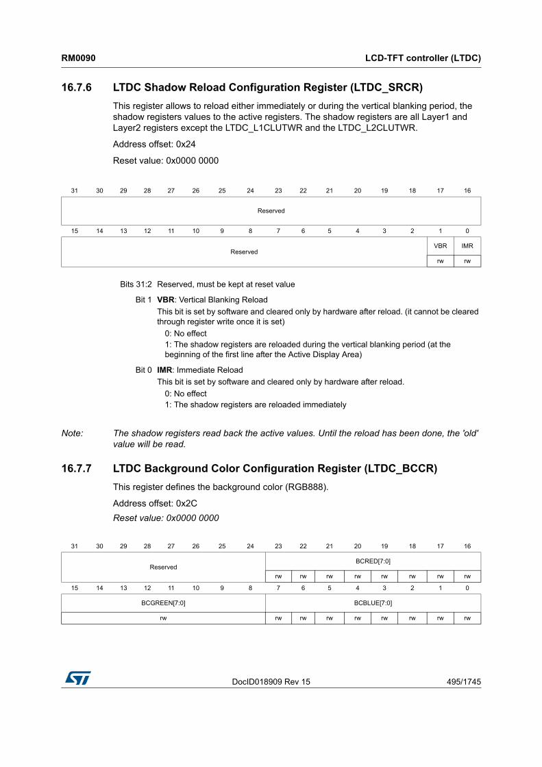
16.7.6 LTDC Shadow Reload Configuration Register (LTDC_SRCR)
This register allows to reload either immediately or during the vertical blanking period, the shadow registers values to the active registers. The shadow registers are all Layer1 and Layer2 registers except the LTDC_L1CLUTWR and the LTDC_L2CLUTWR.
Address offset: 0x24
Reset value: 0x0000 0000
Note: The shadow registers read back the active values. Until the reload has been done, the 'old' value will be read.
16.7.7 LTDC Background Color Configuration Register (LTDC_BCCR)
This register defines the background color (RGB888).
Address offset: 0x2C
Reset value: 0x0000 0000
31 30 29 28 27 26 25 24 23 22 21 20 19 18 17 16
Reserved
15 14 13 12 11 10 9 8 7 6 5 4 3 2 1 0
ReservedVBR IMR
rw rw
Bits 31:2 Reserved, must be kept at reset value
Bit 1 VBR: Vertical Blanking Reload
This bit is set by software and cleared only by hardware after reload. (it cannot be cleared through register write once it is set)
0: No effect1: The shadow registers are reloaded during the vertical blanking period (at the beginning of the first line after the Active Display Area)
Bit 0 IMR: Immediate Reload
This bit is set by software and cleared only by hardware after reload.
0: No effect1: The shadow registers are reloaded immediately
31 30 29 28 27 26 25 24 23 22 21 20 19 18 17 16
ReservedBCRED[7:0]
rw rw rw rw rw rw rw rw
15 14 13 12 11 10 9 8 7 6 5 4 3 2 1 0
BCGREEN[7:0] BCBLUE[7:0]
rw rw rw rw rw rw rw rw rw
LCD-TFT controller (LTDC) RM0090
496/1745 DocID018909 Rev 15
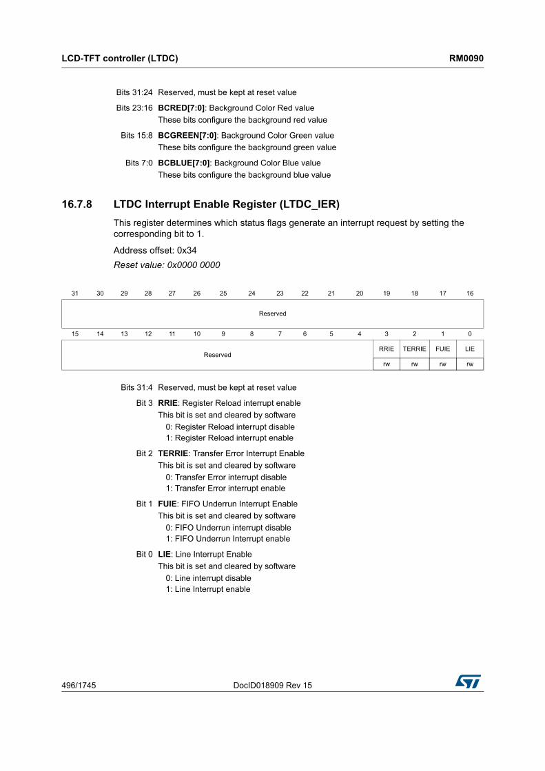
16.7.8 LTDC Interrupt Enable Register (LTDC_IER)
This register determines which status flags generate an interrupt request by setting the corresponding bit to 1.
Address offset: 0x34
Reset value: 0x0000 0000
Bits 31:24 Reserved, must be kept at reset value
Bits 23:16 BCRED[7:0]: Background Color Red value
These bits configure the background red value
Bits 15:8 BCGREEN[7:0]: Background Color Green value
These bits configure the background green value
Bits 7:0 BCBLUE[7:0]: Background Color Blue value
These bits configure the background blue value
31 30 29 28 27 26 25 24 23 22 21 20 19 18 17 16
Reserved
15 14 13 12 11 10 9 8 7 6 5 4 3 2 1 0
ReservedRRIE TERRIE FUIE LIE
rw rw rw rw
Bits 31:4 Reserved, must be kept at reset value
Bit 3 RRIE: Register Reload interrupt enable
This bit is set and cleared by software
0: Register Reload interrupt disable1: Register Reload interrupt enable
Bit 2 TERRIE: Transfer Error Interrupt Enable
This bit is set and cleared by software
0: Transfer Error interrupt disable1: Transfer Error interrupt enable
Bit 1 FUIE: FIFO Underrun Interrupt Enable
This bit is set and cleared by software
0: FIFO Underrun interrupt disable1: FIFO Underrun Interrupt enable
Bit 0 LIE: Line Interrupt Enable
This bit is set and cleared by software
0: Line interrupt disable1: Line Interrupt enable

DocID018909 Rev 15 497/1745
RM0090 LCD-TFT controller (LTDC)
512
16.7.9 LTDC Interrupt Status Register (LTDC_ISR)
This register returns the interrupt status flag
Address offset: 0x38
Reset value: 0x0000 0000
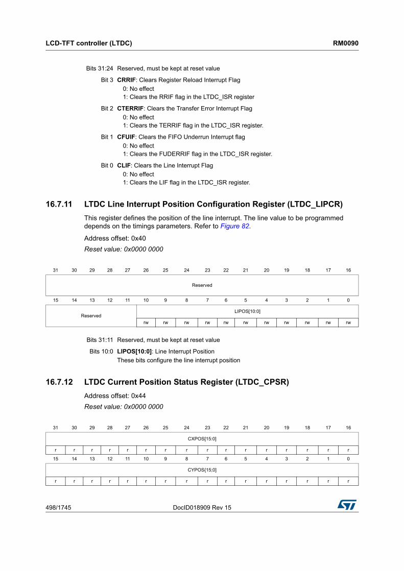
16.7.10 LTDC Interrupt Clear Register (LTDC_ICR)
Address offset: 0x3C
Reset value: 0x0000 0000
31 30 29 28 27 26 25 24 23 22 21 20 19 18 17 16
Reserved
15 14 13 12 11 10 9 8 7 6 5 4 3 2 1 0
ReservedRRIF TERRIF FUIF LIF
r r r r
Bits 31:24 Reserved, must be kept at reset value
Bit 3 RRIF: Register Reload Interrupt Flag
0: No Register Reload interrupt generated1: Register Reload interrupt generated when a vertical blanking reload occurs (and the first line after the active area is reached)
Bit 2 TERRIF: Transfer Error interrupt flag
0: No Transfer Error interrupt generated1: Transfer Error interrupt generated when a Bus error occurs
Bit 1 FUIF: FIFO Underrun Interrupt flag
0: NO FIFO Underrun interrupt generated.1: A FIFO underrun interrupt is generated, if one of the layer FIFOs is empty and pixel data is read from the FIFO
Bit 0 LIF: Line Interrupt flag
0: No Line interrupt generated1: A Line interrupt is generated, when a programmed line is reached
31 30 29 28 27 26 25 24 23 22 21 20 19 18 17 16
Reserved
15 14 13 12 11 10 9 8 7 6 5 4 3 2 1 0
ReservedCRRIF CTERRIF CFUIF CLIF
w w w w
LCD-TFT controller (LTDC) RM0090
498/1745 DocID018909 Rev 15
16.7.11 LTDC Line Interrupt Position Configuration Register (LTDC_LIPCR)
This register defines the position of the line interrupt. The line value to be programmed depends on the timings parameters. Refer to Figure 82.
Address offset: 0x40
Reset value: 0x0000 0000
16.7.12 LTDC Current Position Status Register (LTDC_CPSR)
Address offset: 0x44
Reset value: 0x0000 0000
Bits 31:24 Reserved, must be kept at reset value
Bit 3 CRRIF: Clears Register Reload Interrupt Flag
0: No effect1: Clears the RRIF flag in the LTDC_ISR register
Bit 2 CTERRIF: Clears the Transfer Error Interrupt Flag
0: No effect1: Clears the TERRIF flag in the LTDC_ISR register.
Bit 1 CFUIF: Clears the FIFO Underrun Interrupt flag
0: No effect1: Clears the FUDERRIF flag in the LTDC_ISR register.
Bit 0 CLIF: Clears the Line Interrupt Flag
0: No effect1: Clears the LIF flag in the LTDC_ISR register.
31 30 29 28 27 26 25 24 23 22 21 20 19 18 17 16
Reserved
15 14 13 12 11 10 9 8 7 6 5 4 3 2 1 0
ReservedLIPOS[10:0]
rw rw rw rw rw rw rw rw rw rw rw
Bits 31:11 Reserved, must be kept at reset value
Bits 10:0 LIPOS[10:0]: Line Interrupt Position
These bits configure the line interrupt position
31 30 29 28 27 26 25 24 23 22 21 20 19 18 17 16
CXPOS[15:0]
r r r r r r r r r r r r r r r r
15 14 13 12 11 10 9 8 7 6 5 4 3 2 1 0
CYPOS{15;0]
r r r r r r r r r r r r r r r r

DocID018909 Rev 15 499/1745
RM0090 LCD-TFT controller (LTDC)
512
16.7.13 LTDC Current Display Status Register (LTDC_CDSR)
This register returns the status of the current display phase which is controlled by the HSYNC, VSYNC, and Horizontal/Vertical DE signals.
Example: if the current display phase is the vertical synchronization, the VSYNCS bit is set (active high). If the current display phase is the horizontal synchronization, the HSYNCS bit is active high.
Address offset: 0x48
Reset value: 0x0000 000F
Note: The returned status does not depend on the configured polarity in the LTDC_GCR register, instead it returns the current active display phase.
Bits 31:16: CXPOS[15:0]: Current X Position
These bits return the current X position
Bits 15:0 CYPOS[15:0]: Current Y Position
These bits return the current Y position
31 30 29 28 27 26 25 24 23 22 21 20 19 18 17 16
Reserved
15 14 13 12 11 10 9 8 7 6 5 4 3 2 1 0
Reserved
HSYNCS
VSYNCS
HDES VDES
r r r r
Bits 31:24 Reserved, must be kept at reset value
Bit 3 HSYNCS: Horizontal Synchronization display Status
0: Active low 1: Active high
Bit 2 VSYNCS: Vertical Synchronization display Status
0: Active low 1: Active high
Bit 1 HDES: Horizontal Data Enable display Status
0: Active low 1: Active high
Bit 0 VDES: Vertical Data Enable display Status
0: Active low 1: Active high
LCD-TFT controller (LTDC) RM0090
500/1745 DocID018909 Rev 15
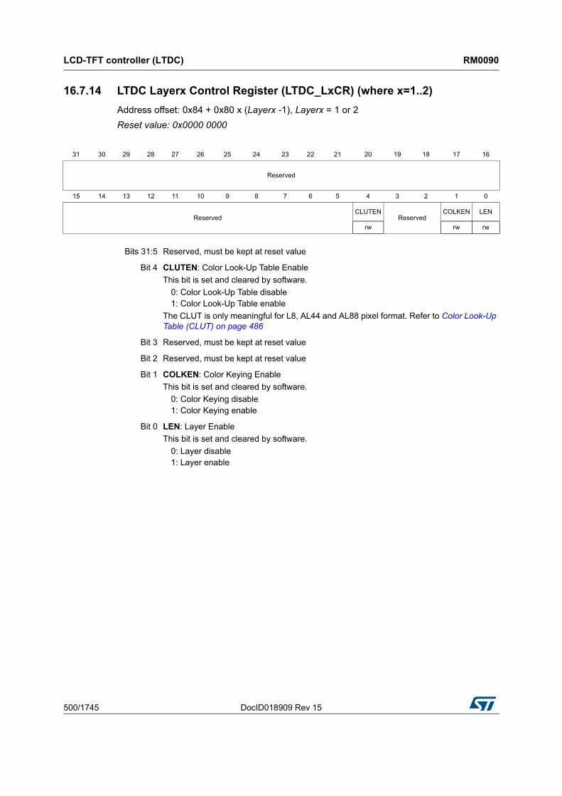
16.7.14 LTDC Layerx Control Register (LTDC_LxCR) (where x=1..2)
Address offset: 0x84 + 0x80 x (Layerx -1), Layerx = 1 or 2
Reset value: 0x0000 0000
31 30 29 28 27 26 25 24 23 22 21 20 19 18 17 16
Reserved
15 14 13 12 11 10 9 8 7 6 5 4 3 2 1 0
ReservedCLUTEN
ReservedCOLKEN LEN
rw rw rw
Bits 31:5 Reserved, must be kept at reset value
Bit 4 CLUTEN: Color Look-Up Table Enable
This bit is set and cleared by software.
0: Color Look-Up Table disable1: Color Look-Up Table enable
The CLUT is only meaningful for L8, AL44 and AL88 pixel format. Refer to Color Look-Up Table (CLUT) on page 486
Bit 3 Reserved, must be kept at reset value
Bit 2 Reserved, must be kept at reset value
Bit 1 COLKEN: Color Keying Enable
This bit is set and cleared by software.
0: Color Keying disable1: Color Keying enable
Bit 0 LEN: Layer Enable
This bit is set and cleared by software.
0: Layer disable1: Layer enable
DocID018909 Rev 15 501/1745
RM0090 LCD-TFT controller (LTDC)
512
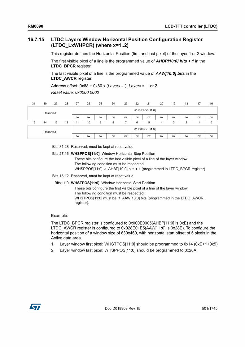
16.7.15 LTDC Layerx Window Horizontal Position Configuration Register(LTDC_LxWHPCR) (where x=1..2)
This register defines the Horizontal Position (first and last pixel) of the layer 1 or 2 window.
The first visible pixel of a line is the programmed value of AHBP[10:0] bits + 1 in the LTDC_BPCR register.
The last visible pixel of a line is the programmed value of AAW[10:0] bits in the LTDC_AWCR register.
Address offset: 0x88 + 0x80 x (Layerx -1), Layerx = 1 or 2
Reset value: 0x0000 0000
Example:
The LTDC_BPCR register is configured to 0x000E0005(AHBP[11:0] is 0xE) and the LTDC_AWCR register is configured to 0x028E01E5(AAW[11:0] is 0x28E). To configure the horizontal position of a window size of 630x460, with horizontal start offset of 5 pixels in the Active data area.
1. Layer window first pixel: WHSTPOS[11:0] should be programmed to 0x14 (0xE+1+0x5)
2. Layer window last pixel: WHSPPOS[11:0] should be programmed to 0x28A
31 30 29 28 27 26 25 24 23 22 21 20 19 18 17 16
ReservedWHSPPOS[11:0]
rw rw rw rw rw rw rw rw rw rw rw rw
15 14 13 12 11 10 9 8 7 6 5 4 3 2 1 0
ReservedWHSTPOS[11:0]
rw rw rw rw rw rw rw rw rw rw rw rw
Bits 31:28 Reserved, must be kept at reset value
Bits 27:16 WHSPPOS[11:0]: Window Horizontal Stop Position
These bits configure the last visible pixel of a line of the layer window.The following condition must be respected: WHSPPOS[11:0] ≥ AHBP[10:0] bits + 1 (programmed in LTDC_BPCR register)
Bits 15:12 Reserved, must be kept at reset value
Bits 11:0 WHSTPOS[11:0]: Window Horizontal Start Position
These bits configure the first visible pixel of a line of the layer window.The following condition must be respected: WHSTPOS[11:0] must be ≤ AAW[10:0] bits (programmed in the LTDC_AWCR register).
LCD-TFT controller (LTDC) RM0090
502/1745 DocID018909 Rev 15
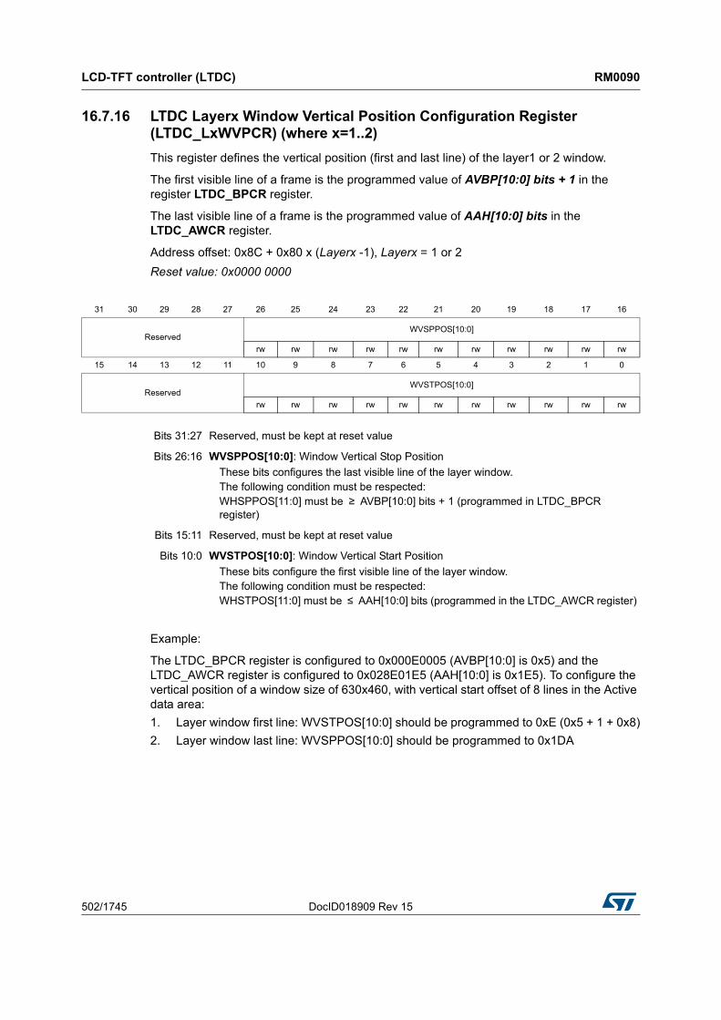
16.7.16 LTDC Layerx Window Vertical Position Configuration Register(LTDC_LxWVPCR) (where x=1..2)
This register defines the vertical position (first and last line) of the layer1 or 2 window.
The first visible line of a frame is the programmed value of AVBP[10:0] bits + 1 in the register LTDC_BPCR register.
The last visible line of a frame is the programmed value of AAH[10:0] bits in the LTDC_AWCR register.
Address offset: 0x8C + 0x80 x (Layerx -1), Layerx = 1 or 2
Reset value: 0x0000 0000
Example:
The LTDC_BPCR register is configured to 0x000E0005 (AVBP[10:0] is 0x5) and the LTDC_AWCR register is configured to 0x028E01E5 (AAH[10:0] is 0x1E5). To configure the vertical position of a window size of 630x460, with vertical start offset of 8 lines in the Active data area:
1. Layer window first line: WVSTPOS[10:0] should be programmed to 0xE (0x5 + 1 + 0x8)
2. Layer window last line: WVSPPOS[10:0] should be programmed to 0x1DA
31 30 29 28 27 26 25 24 23 22 21 20 19 18 17 16
ReservedWVSPPOS[10:0]
rw rw rw rw rw rw rw rw rw rw rw
15 14 13 12 11 10 9 8 7 6 5 4 3 2 1 0
ReservedWVSTPOS[10:0]
rw rw rw rw rw rw rw rw rw rw rw
Bits 31:27 Reserved, must be kept at reset value
Bits 26:16 WVSPPOS[10:0]: Window Vertical Stop Position
These bits configures the last visible line of the layer window. The following condition must be respected: WHSPPOS[11:0] must be ≥ AVBP[10:0] bits + 1 (programmed in LTDC_BPCR register)
Bits 15:11 Reserved, must be kept at reset value
Bits 10:0 WVSTPOS[10:0]: Window Vertical Start Position
These bits configure the first visible line of the layer window.The following condition must be respected: WHSTPOS[11:0] must be ≤ AAH[10:0] bits (programmed in the LTDC_AWCR register)
DocID018909 Rev 15 503/1745
RM0090 LCD-TFT controller (LTDC)
512
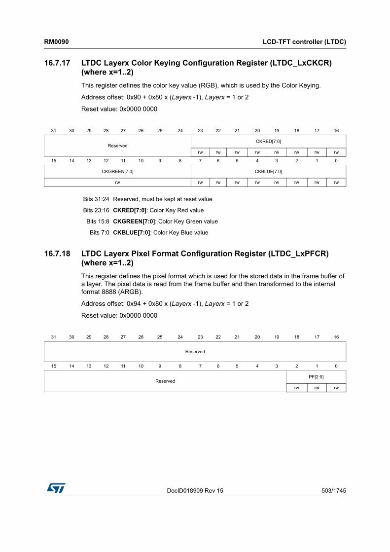
16.7.17 LTDC Layerx Color Keying Configuration Register (LTDC_LxCKCR)(where x=1..2)
This register defines the color key value (RGB), which is used by the Color Keying.
Address offset: 0x90 + 0x80 x (Layerx -1), Layerx = 1 or 2
Reset value: 0x0000 0000
16.7.18 LTDC Layerx Pixel Format Configuration Register (LTDC_LxPFCR)(where x=1..2)
This register defines the pixel format which is used for the stored data in the frame buffer of a layer. The pixel data is read from the frame buffer and then transformed to the internal format 8888 (ARGB).
Address offset: 0x94 + 0x80 x (Layerx -1), Layerx = 1 or 2
Reset value: 0x0000 0000
31 30 29 28 27 26 25 24 23 22 21 20 19 18 17 16
ReservedCKRED[7:0]
rw rw rw rw rw rw rw rw
15 14 13 12 11 10 9 8 7 6 5 4 3 2 1 0
CKGREEN[7:0] CKBLUE[7:0]
rw rw rw rw rw rw rw rw rw
Bits 31:24 Reserved, must be kept at reset value
Bits 23:16 CKRED[7:0]: Color Key Red value
Bits 15:8 CKGREEN[7:0]: Color Key Green value
Bits 7:0 CKBLUE[7:0]: Color Key Blue value
31 30 29 28 27 26 25 24 23 22 21 20 19 18 17 16
Reserved
15 14 13 12 11 10 9 8 7 6 5 4 3 2 1 0
ReservedPF[2:0]
rw rw rw
LCD-TFT controller (LTDC) RM0090
504/1745 DocID018909 Rev 15
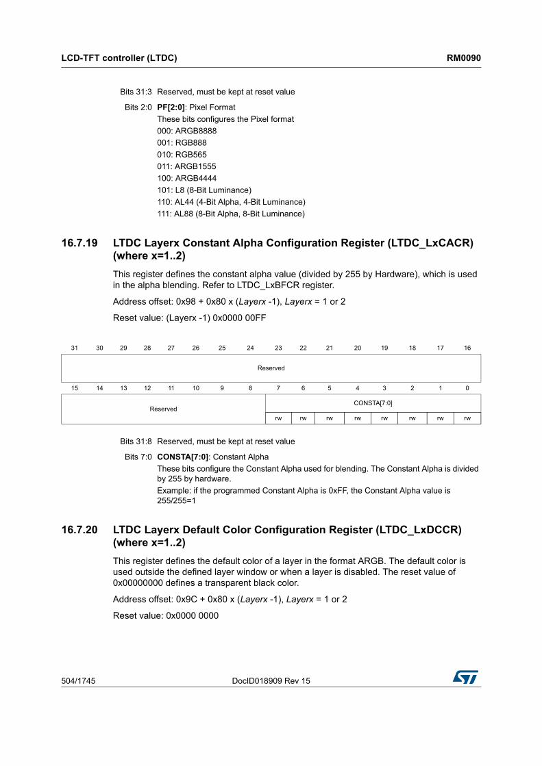
16.7.19 LTDC Layerx Constant Alpha Configuration Register (LTDC_LxCACR)(where x=1..2)
This register defines the constant alpha value (divided by 255 by Hardware), which is used in the alpha blending. Refer to LTDC_LxBFCR register.
Address offset: 0x98 + 0x80 x (Layerx -1), Layerx = 1 or 2
Reset value: (Layerx -1) 0x0000 00FF
16.7.20 LTDC Layerx Default Color Configuration Register (LTDC_LxDCCR)(where x=1..2)
This register defines the default color of a layer in the format ARGB. The default color is used outside the defined layer window or when a layer is disabled. The reset value of 0x00000000 defines a transparent black color.
Address offset: 0x9C + 0x80 x (Layerx -1), Layerx = 1 or 2
Reset value: 0x0000 0000
Bits 31:3 Reserved, must be kept at reset value
Bits 2:0 PF[2:0]: Pixel Format
These bits configures the Pixel format
000: ARGB8888
001: RGB888
010: RGB565
011: ARGB1555
100: ARGB4444
101: L8 (8-Bit Luminance)
110: AL44 (4-Bit Alpha, 4-Bit Luminance)
111: AL88 (8-Bit Alpha, 8-Bit Luminance)
31 30 29 28 27 26 25 24 23 22 21 20 19 18 17 16
Reserved
15 14 13 12 11 10 9 8 7 6 5 4 3 2 1 0
ReservedCONSTA[7:0]
rw rw rw rw rw rw rw rw
Bits 31:8 Reserved, must be kept at reset value
Bits 7:0 CONSTA[7:0]: Constant Alpha
These bits configure the Constant Alpha used for blending. The Constant Alpha is divided by 255 by hardware.
Example: if the programmed Constant Alpha is 0xFF, the Constant Alpha value is 255/255=1
DocID018909 Rev 15 505/1745
RM0090 LCD-TFT controller (LTDC)
512
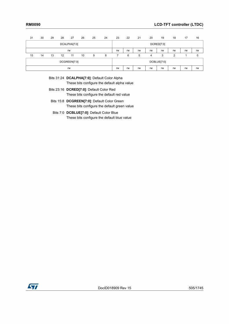
31 30 29 28 27 26 25 24 23 22 21 20 19 18 17 16
DCALPHA[7:0] DCRED[7:0]
rw rw rw rw rw rw rw rw rw
15 14 13 12 11 10 9 8 7 6 5 4 3 2 1 0
DCGREEN[7:0] DCBLUE[7:0]
rw rw rw rw rw rw rw rw rw
Bits 31:24 DCALPHA[7:0]: Default Color Alpha
These bits configure the default alpha value
Bits 23:16 DCRED[7:0]: Default Color Red
These bits configure the default red value
Bits 15:8 DCGREEN[7:0]: Default Color Green
These bits configure the default green value
Bits 7:0 DCBLUE[7:0]: Default Color Blue
These bits configure the default blue value
LCD-TFT controller (LTDC) RM0090
506/1745 DocID018909 Rev 15
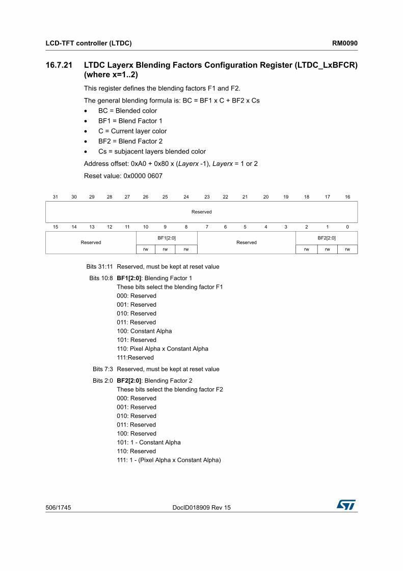
16.7.21 LTDC Layerx Blending Factors Configuration Register (LTDC_LxBFCR)(where x=1..2)
This register defines the blending factors F1 and F2.
The general blending formula is: BC = BF1 x C + BF2 x Cs
• BC = Blended color
• BF1 = Blend Factor 1
• C = Current layer color
• BF2 = Blend Factor 2
• Cs = subjacent layers blended color
Address offset: 0xA0 + 0x80 x (Layerx -1), Layerx = 1 or 2
Reset value: 0x0000 0607
31 30 29 28 27 26 25 24 23 22 21 20 19 18 17 16
Reserved
15 14 13 12 11 10 9 8 7 6 5 4 3 2 1 0
ReservedBF1[2:0]
ReservedBF2[2:0]
rw rw rw rw rw rw
Bits 31:11 Reserved, must be kept at reset value
Bits 10:8 BF1[2:0]: Blending Factor 1
These bits select the blending factor F1
000: Reserved
001: Reserved
010: Reserved
011: Reserved
100: Constant Alpha
101: Reserved
110: Pixel Alpha x Constant Alpha
111:Reserved
Bits 7:3 Reserved, must be kept at reset value
Bits 2:0 BF2[2:0]: Blending Factor 2
These bits select the blending factor F2
000: Reserved
001: Reserved
010: Reserved
011: Reserved
100: Reserved
101: 1 - Constant Alpha
110: Reserved
111: 1 - (Pixel Alpha x Constant Alpha)

DocID018909 Rev 15 507/1745
RM0090 LCD-TFT controller (LTDC)
512
Note: The Constant Alpha value, is the programmed value in the LxCACR register divided by 255 by hardware.
Example: Only layer1 is enabled, BF1 configured to Constant Alpha
BF2 configured to 1 - Constant Alpha
Constant Alpha: The Constant Alpha programmed in the LxCACR register is 240 (0xF0). Thus, the Constant Alpha value is 240/255 = 0.94
C: Current Layer Color is 128
Cs: Background color is 48
Layer1 is blended with the background color.
BC = Constant Alpha x C + (1 - Constant Alpha) x Cs = 0.94 x 128 + (1- 0.94) x 48 = 123.
16.7.22 LTDC Layerx Color Frame Buffer Address Register (LTDC_LxCFBAR)(where x=1..2)
This register defines the color frame buffer start address which has to point to the address where the pixel data of the top left pixel of a layer is stored in the frame buffer.
Address offset: 0xAC + 0x80 x (Layerx -1), Layerx = 1 or 2
Reset value: 0x0000 0000
16.7.23 LTDC Layerx Color Frame Buffer Length Register (LTDC_LxCFBLR)(where x=1..2)
This register defines the color frame buffer line length and pitch.
Address offset: 0xB0 + 0x80 x (Layerx -1), Layerx = 1 or 2
Reset value: 0x0000 0000
31 30 29 28 27 26 25 24 23 22 21 20 19 18 17 16
CFBADD[31:0]
rw rw rw rw rw rw rw rw rw rw rw rw rw rw rw rw
15 14 13 12 11 10 9 8 7 6 5 4 3 2 1 0
CFBADD[31:0]
rw rw rw rw rw rw rw rw rw rw rw rw rw rw rw rw
Bits 31:0 CFBADD[31:0]: Color Frame Buffer Start Address
These bits defines the color frame buffer start address.
31 30 29 28 27 26 25 24 23 22 21 20 19 18 17 16
ReservedCFBP[12:0]
rw rw rw rw rw rw rw rw rw rw rw rw rw
15 14 13 12 11 10 9 8 7 6 5 4 3 2 1 0
ReservedCFBLL[12:0]
rw rw rw rw rw rw rw rw rw rw rw rw rw
LCD-TFT controller (LTDC) RM0090
508/1745 DocID018909 Rev 15
Example:
• A frame buffer having the format RGB565 (2 bytes per pixel) and a width of 256 pixels (total number of bytes per line is 256x2=512 bytes), where pitch = line length requires a value of 0x02000203 to be written into this register.
• A frame buffer having the format RGB888 (3 bytes per pixel) and a width of 320 pixels (total number of bytes per line is 320x3=960), where pitch = line length requires a value of 0x03C003C3 to be written into this register.
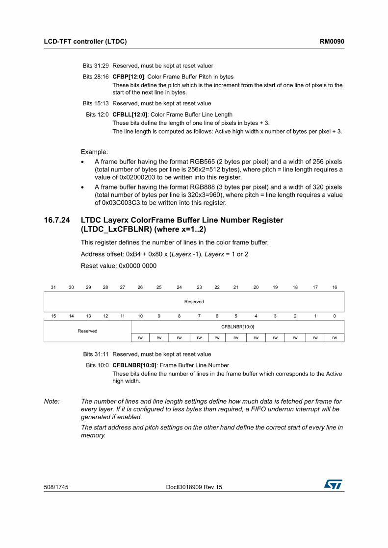
16.7.24 LTDC Layerx ColorFrame Buffer Line Number Register(LTDC_LxCFBLNR) (where x=1..2)
This register defines the number of lines in the color frame buffer.
Address offset: 0xB4 + 0x80 x (Layerx -1), Layerx = 1 or 2
Reset value: 0x0000 0000
Note: The number of lines and line length settings define how much data is fetched per frame for every layer. If it is configured to less bytes than required, a FIFO underrun interrupt will be generated if enabled.
The start address and pitch settings on the other hand define the correct start of every line in memory.
Bits 31:29 Reserved, must be kept at reset valuer
Bits 28:16 CFBP[12:0]: Color Frame Buffer Pitch in bytes
These bits define the pitch which is the increment from the start of one line of pixels to the start of the next line in bytes.
Bits 15:13 Reserved, must be kept at reset value
Bits 12:0 CFBLL[12:0]: Color Frame Buffer Line Length
These bits define the length of one line of pixels in bytes + 3.
The line length is computed as follows: Active high width x number of bytes per pixel + 3.
31 30 29 28 27 26 25 24 23 22 21 20 19 18 17 16
Reserved
15 14 13 12 11 10 9 8 7 6 5 4 3 2 1 0
ReservedCFBLNBR[10:0]
rw rw rw rw rw rw rw rw rw rw rw
Bits 31:11 Reserved, must be kept at reset value
Bits 10:0 CFBLNBR[10:0]: Frame Buffer Line Number
These bits define the number of lines in the frame buffer which corresponds to the Active high width.

DocID018909 Rev 15 509/1745
RM0090 LCD-TFT controller (LTDC)
512
16.7.25 LTDC Layerx CLUT Write Register (LTDC_LxCLUTWR) (where x=1..2)
This register defines the CLUT address and the RGB value.
Address offset: 0xC4 + 0x80 x (Layerx -1), Layerx = 1 or 2
Reset value: 0x0000 0000
Note: The CLUT write register should only be configured during blanking period or if the layer is disabled. The CLUT can be enabled or disabled in the LTDC_LxCR register.
The CLUT is only meaningful for L8, AL44 and AL88 pixel format.
31 30 29 28 27 26 25 24 23 22 21 20 19 18 17 16
CLUTADD[7:0] RED[7:0]
w w w w w w w w w w w w w w w w
15 14 13 12 11 10 9 8 7 6 5 4 3 2 1 0
GREEN[7:0] BLUE[7:0]
w w w w w w w w w w w w w w w w
Bits 31:24 CLUTADD[7:0]: CLUT Address
These bits configure the CLUT address (color position within the CLUT) of each RGB value
Bits 23:16 RED[7:0]: Red value
These bits configure the red value
Bits 15:8 GREEN[7:0]: Green value
These bits configure the green value
Bits 7:0 BLUE[7:0]: Blue value
These bits configure the blue value
LCD-TFT controller (LTDC) RM0090
510/1745 DocID018909 Rev 15
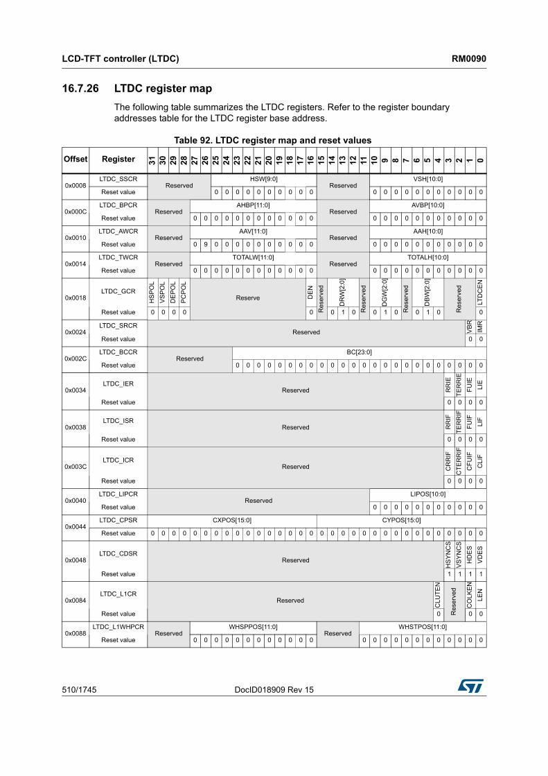
16.7.26 LTDC register map
The following table summarizes the LTDC registers. Refer to the register boundary addresses table for the LTDC register base address.
Table 92. LTDC register map and reset values
Offset Register 31
30
29
28
27
26
25
24
23
22
21
20
19
18
17
16
15
14
13
12 11 10 9 8 7 6 5 4 3 2 1 0
0x0008LTDC_SSCR
ReservedHSW[9:0]
ReservedVSH[10:0]
Reset value 0 0 0 0 0 0 0 0 0 0 0 0 0 0 0 0 0 0 0 0 0
0x000CLTDC_BPCR
ReservedAHBP[11:0]
ReservedAVBP[10:0]
Reset value 0 0 0 0 0 0 0 0 0 0 0 0 0 0 0 0 0 0 0 0 0 0 0
0x0010LTDC_AWCR
ReservedAAV[11:0]
ReservedAAH[10:0]
Reset value 0 9 0 0 0 0 0 0 0 0 0 0 0 0 0 0 0 0 0 0 0 0 0
0x0014LTDC_TWCR
ReservedTOTALW[11:0]
ReservedTOTALH[10:0]
Reset value 0 0 0 0 0 0 0 0 0 0 0 0 0 0 0 0 0 0 0 0 0 0 0
0x0018LTDC_GCR
HS
PO
L
VS
PO
L
DE
PO
L
PC
PO
L
Reserve DE
N
Re
serv
ed
DR
W[2
:0]
Re
serv
ed
DG
W[2
:0]
Re
serv
ed
DB
W[2
:0]
Re
serv
ed
LTD
CE
N
Reset value 0 0 0 0 0 0 1 0 0 1 0 0 1 0 0
0x0024LTDC_SRCR
Reserved VB
R
IMR
Reset value 0 0
0x002CLTDC_BCCR
ReservedBC[23:0]
Reset value 0 0 0 0 0 0 0 0 0 0 0 0 0 0 0 0 0 0 0 0 0 0 0 0
0x0034LTDC_IER
Reserved RR
IE
TE
RR
IE
FU
IE
LIE
Reset value 0 0 0 0
0x0038LTDC_ISR
Reserved RR
IF
TE
RR
IF
FU
IF
LIF
Reset value 0 0 0 0
0x003CLTDC_ICR
Reserved CR
RIF
CT
ER
RIF
CF
UIF
CL
IFReset value 0 0 0 0
0x0040LTDC_LIPCR
ReservedLIPOS[10:0]
Reset value 0 0 0 0 0 0 0 0 0 0 0
0x0044LTDC_CPSR CXPOS[15:0] CYPOS[15:0]
Reset value 0 0 0 0 0 0 0 0 0 0 0 0 0 0 0 0 0 0 0 0 0 0 0 0 0 0 0 0 0 0 0 0
0x0048LTDC_CDSR
Reserved
HS
YN
CS
VS
YN
CS
HD
ES
VD
ES
Reset value 1 1 1 1
0x0084LTDC_L1CR
Reserved
CL
UT
EN
Re
serv
ed
CO
LK
EN
LE
N
Reset value 0 0 0
0x0088LTDC_L1WHPCR
ReservedWHSPPOS[11:0]
ReservedWHSTPOS[11:0]
Reset value 0 0 0 0 0 0 0 0 0 0 0 0 0 0 0 0 0 0 0 0 0 0 0 0
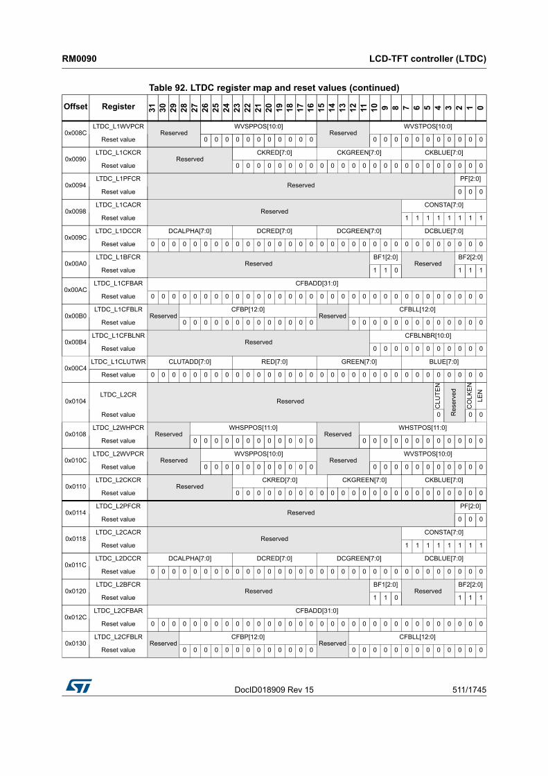
DocID018909 Rev 15 511/1745
RM0090 LCD-TFT controller (LTDC)
512
0x008CLTDC_L1WVPCR
ReservedWVSPPOS[10:0]
ReservedWVSTPOS[10:0]
Reset value 0 0 0 0 0 0 0 0 0 0 0 0 0 0 0 0 0 0 0 0 0 0
0x0090LTDC_L1CKCR
ReservedCKRED[7:0] CKGREEN[7:0] CKBLUE[7:0]
Reset value 0 0 0 0 0 0 0 0 0 0 0 0 0 0 0 0 0 0 0 0 0 0 0 0
0x0094LTDC_L1PFCR
ReservedPF[2:0]
Reset value 0 0 0
0x0098LTDC_L1CACR
ReservedCONSTA[7:0]
Reset value 1 1 1 1 1 1 1 1
0x009CLTDC_L1DCCR DCALPHA[7:0] DCRED[7:0] DCGREEN[7:0] DCBLUE[7:0]
Reset value 0 0 0 0 0 0 0 0 0 0 0 0 0 0 0 0 0 0 0 0 0 0 0 0 0 0 0 0 0 0 0 0
0x00A0LTDC_L1BFCR
ReservedBF1[2:0]
ReservedBF2[2:0]
Reset value 1 1 0 1 1 1
0x00ACLTDC_L1CFBAR CFBADD[31:0]
Reset value 0 0 0 0 0 0 0 0 0 0 0 0 0 0 0 0 0 0 0 0 0 0 0 0 0 0 0 0 0 0 0 0
0x00B0LTDC_L1CFBLR
ReservedCFBP[12:0]
ReservedCFBLL[12:0]
Reset value 0 0 0 0 0 0 0 0 0 0 0 0 0 0 0 0 0 0 0 0 0 0 0 0 0 0
0x00B4LTDC_L1CFBLNR
ReservedCFBLNBR[10:0]
Reset value 0 0 0 0 0 0 0 0 0 0 0
0x00C4LTDC_L1CLUTWR CLUTADD[7:0] RED[7:0] GREEN[7:0] BLUE[7:0]
Reset value 0 0 0 0 0 0 0 0 0 0 0 0 0 0 0 0 0 0 0 0 0 0 0 0 0 0 0 0 0 0 0 0
0x0104LTDC_L2CR
Reserved
CL
UT
EN
Re
serv
ed
CO
LK
EN
LE
N
Reset value 0 0 0
0x0108LTDC_L2WHPCR
ReservedWHSPPOS[11:0]
ReservedWHSTPOS[11:0]
Reset value 0 0 0 0 0 0 0 0 0 0 0 0 0 0 0 0 0 0 0 0 0 0 0 0
0x010CLTDC_L2WVPCR
ReservedWVSPPOS[10:0]
ReservedWVSTPOS[10:0]
Reset value 0 0 0 0 0 0 0 0 0 0 0 0 0 0 0 0 0 0 0 0 0 0
0x0110LTDC_L2CKCR
ReservedCKRED[7:0] CKGREEN[7:0] CKBLUE[7:0]
Reset value 0 0 0 0 0 0 0 0 0 0 0 0 0 0 0 0 0 0 0 0 0 0 0 0
0x0114LTDC_L2PFCR
ReservedPF[2:0]
Reset value 0 0 0
0x0118LTDC_L2CACR
ReservedCONSTA[7:0]
Reset value 1 1 1 1 1 1 1 1
0x011CLTDC_L2DCCR DCALPHA[7:0] DCRED[7:0] DCGREEN[7:0] DCBLUE[7:0]
Reset value 0 0 0 0 0 0 0 0 0 0 0 0 0 0 0 0 0 0 0 0 0 0 0 0 0 0 0 0 0 0 0 0
0x0120LTDC_L2BFCR
ReservedBF1[2:0]
ReservedBF2[2:0]
Reset value 1 1 0 1 1 1
0x012CLTDC_L2CFBAR CFBADD[31:0]
Reset value 0 0 0 0 0 0 0 0 0 0 0 0 0 0 0 0 0 0 0 0 0 0 0 0 0 0 0 0 0 0 0 0
0x0130LTDC_L2CFBLR
ReservedCFBP[12:0]
ReservedCFBLL[12:0]
Reset value 0 0 0 0 0 0 0 0 0 0 0 0 0 0 0 0 0 0 0 0 0 0 0 0 0 0
Table 92. LTDC register map and reset values (continued)
Offset Register 31
30
29
28
27
26
25
24
23
22
21
20
19
18
17
16
15
14
13
12 11 10 9 8 7 6 5 4 3 2 1 0

LCD-TFT controller (LTDC) RM0090
512/1745 DocID018909 Rev 15
0x0134LTDC_L2CFBLNR
ReservedCFBLNBR[10:0]
Reset value 0 0 0 0 0 0 0 0 0 0 0
0x0144LTDC_L2CLUTWR CLUTADD[7:0] RED[7:0] GREEN[7:0] BLUE[7:0]
Reset value 0 0 0 0 0 0 0 0 0 0 0 0 0 0 0 0 0 0 0 0 0 0 0 0 0 0 0 0 0 0 0 0
Table 92. LTDC register map and reset values (continued)
Offset Register 31
30
29
28
27
26
25
24
23
22
21
20
19
18
17
16
15
14
13
12 11 10 9 8 7 6 5 4 3 2 1 0