1747-6.1, data table access module, user manualcolumbiamachine.com/docs/knowledge-base/plc_1747_dtam...
TRANSCRIPT

User Manual
Data Table Access Module(Cat. No. 1747-DTAM-E)
Allen-Bradley
Important User Information
Because of the variety of uses for the products described in this publication, those responsible for the application and use of this control equipment must satisfy themselves that all necessary steps have been taken to assure that each application and use meets all performance and safety requirements, including any applicable laws, regulations, codes and standards.
The illustrations, charts, sample programs and layout examples shown in this guide are intended solely for purposes of example. Since there are many variables and requirements associated with any particular installation, Allen-Bradley does not assume responsibility or liability (to include intellectual property liability) for actual use based upon the examples shown in this publication.
Allen-Bradley publication SGI-1.1, Safety Guidelines for the Application, Installation and Maintenance of Solid-State Control (available from your local Allen-Bradley office), describes some important differences between solid-state equipment and electromechanical devices that should be taken into consideration when applying products such as those described in this publication.
Reproduction of the contents of this copyrighted publication, in whole or part, without written permission of Allen-Bradley Company, Inc., is prohibited.
Throughout this manual we use notes to make you aware of safety considerations:
Attention statements help you to:
• identify a hazard
• avoid a hazard
• recognize the consequences
!ATTENTION: Identifies information about practices or circumstances that can lead to personal injury or death, property damage or economic loss.
Important: Identifies information that is critical for successful application and understanding of the product.
PLC, PLC2, PLC3, and PLC5 are registered trademarks of Rockwell Automation.SLC, SLC500, PanelView, RediPANEL, and Dataliner are trademarks of Rockwell Automation.IBM is a registered trademark of International Business Machines, Inc.

Summary of Changes
The information below summarizes the changes to this manual since the last printing.
To help you find new information and updated information in this release of the manual, we have included change bars as shown to the right of this paragraph.
New Information The table below lists sections that document new features and provide additional information about existing features, and it shows where to find this new information.
For New Information On See Chapter
Because users may employ different programming devices, specific references to Advanced Programming Software have been removed from this manual.
Preface – Related Documentation Table and/or Your Software User Manual
Chapter 8 – Message Capability
Notice of Class I, Division 2, Groups A, B, C, D Hazardous Location Certification
Chapter 1 – Data Table Access Module Overview
Appendix A – Specifications
An updated diagram showing the connection of a DTAM module to a DH485 network using a link coupler and an Advanced Interface Converter (1747-NET-AIC).
Chapter 2 – Installation and Power Up
An updated listing of MSG Instruction Error Codes Chapter 9 – Troubleshooting
Publication 1747-6.1

S-2 Summary of Changes
Publication 1747-6.1

Table of Contents iii
Table of ContentsPreface
Who Should Use this Manual . . . . . . . . . . . . . . . . . . . . . . . . . . . . . . . . . . P-1Purpose of this Manual . . . . . . . . . . . . . . . . . . . . . . . . . . . . . . . . . . . . . . . P-1
Contents of this Manual . . . . . . . . . . . . . . . . . . . . . . . . . . . . . . . . . . . . P-2Related Documentation . . . . . . . . . . . . . . . . . . . . . . . . . . . . . . . . . . . . P-3
Common Techniques Used in this Manual . . . . . . . . . . . . . . . . . . . . . . . . P-3Allen-Bradley Support . . . . . . . . . . . . . . . . . . . . . . . . . . . . . . . . . . . . . . . . P-4
Local Product Support . . . . . . . . . . . . . . . . . . . . . . . . . . . . . . . . . . . . . P-4Technical Product Assistance . . . . . . . . . . . . . . . . . . . . . . . . . . . . . . . P-4Your Questions or Comments on this Manual . . . . . . . . . . . . . . . . . . . P-4
Data Table Access Module Overview
Chapter 1Module Overview . . . . . . . . . . . . . . . . . . . . . . . . . . . . . . . . . . . . . . . . . . . 1-1
Installation and Power Up Chapter 2European Union Directive Compliance . . . . . . . . . . . . . . . . . . . . . . . . . . . 2-1
EMC Directive . . . . . . . . . . . . . . . . . . . . . . . . . . . . . . . . . . . . . . . . . . . 2-1Mounting the Module . . . . . . . . . . . . . . . . . . . . . . . . . . . . . . . . . . . . . . . . 2-1Connecting Your Equipment . . . . . . . . . . . . . . . . . . . . . . . . . . . . . . . . . . . 2-4Module Configuration and Adjustments . . . . . . . . . . . . . . . . . . . . . . . . . . 2-6Power-Up Sequence . . . . . . . . . . . . . . . . . . . . . . . . . . . . . . . . . . . . . . . . . 2-8
Module Setup Procedure Chapter 3Keyboard Description . . . . . . . . . . . . . . . . . . . . . . . . . . . . . . . . . . . . . . . . 3-1Factory Default Settings . . . . . . . . . . . . . . . . . . . . . . . . . . . . . . . . . . . . . . 3-2Entering the Setup Mode . . . . . . . . . . . . . . . . . . . . . . . . . . . . . . . . . . . . . 3-3Selecting the Language . . . . . . . . . . . . . . . . . . . . . . . . . . . . . . . . . . . . . . 3-4Selecting the Node Address . . . . . . . . . . . . . . . . . . . . . . . . . . . . . . . . . . . 3-4Setting the Baud Rate . . . . . . . . . . . . . . . . . . . . . . . . . . . . . . . . . . . . . . . . 3-5Setting the Auto Attach Function . . . . . . . . . . . . . . . . . . . . . . . . . . . . . . . 3-5Backlighting the LCD . . . . . . . . . . . . . . . . . . . . . . . . . . . . . . . . . . . . . . . . 3-6Setting the Monitor Override Function . . . . . . . . . . . . . . . . . . . . . . . . . . . 3-6Accepting Module Setup Parameters . . . . . . . . . . . . . . . . . . . . . . . . . . . . 3-7Using the Module Reset . . . . . . . . . . . . . . . . . . . . . . . . . . . . . . . . . . . . . . 3-7
Attaching to a Processor Chapter 4Manual Attach Procedure . . . . . . . . . . . . . . . . . . . . . . . . . . . . . . . . . . . . . 4-1Auto Attach Procedure . . . . . . . . . . . . . . . . . . . . . . . . . . . . . . . . . . . . . . . 4-2Ready Attached Screen . . . . . . . . . . . . . . . . . . . . . . . . . . . . . . . . . . . . . . 4-3
Operating Mode Text . . . . . . . . . . . . . . . . . . . . . . . . . . . . . . . . . . . . . . 4-3Backspace Function During Attach Procedure . . . . . . . . . . . . . . . . . . . . . 4-3Attaching to a Password Protected Processor . . . . . . . . . . . . . . . . . . . . . 4-4
Publication 1747-6.1
iv Table of Contents
Monitoring and Modifying Data
Chapter 5Operating Modes . . . . . . . . . . . . . . . . . . . . . . . . . . . . . . . . . . . . . . . . . . . .5-1
Modify Mode . . . . . . . . . . . . . . . . . . . . . . . . . . . . . . . . . . . . . . . . . . . . .5-1Monitor Mode. . . . . . . . . . . . . . . . . . . . . . . . . . . . . . . . . . . . . . . . . . . . .5-1Monitor Override Feature . . . . . . . . . . . . . . . . . . . . . . . . . . . . . . . . . . .5-1
Logical Data File Addressing . . . . . . . . . . . . . . . . . . . . . . . . . . . . . . . . . . .5-3Backspace Function During Data File Address Entry . . . . . . . . . . . . . . . .5-4Quick Access Addressing . . . . . . . . . . . . . . . . . . . . . . . . . . . . . . . . . . . . .5-5Entering Data File Addresses . . . . . . . . . . . . . . . . . . . . . . . . . . . . . . . . . .5-7
Entering Input and Output Addresses . . . . . . . . . . . . . . . . . . . . . . . . . .5-7Entering Bit Addresses . . . . . . . . . . . . . . . . . . . . . . . . . . . . . . . . . . . . .5-7Entering Timer and Counter Addresses . . . . . . . . . . . . . . . . . . . . . . . .5-7Entering Control Register Addresses . . . . . . . . . . . . . . . . . . . . . . . . . .5-8Entering Integer Addresses . . . . . . . . . . . . . . . . . . . . . . . . . . . . . . . . . .5-8
How to Change Displayed Data File Addresses . . . . . . . . . . . . . . . . . . . .5-9How to Display Higher and Lower Word Addresses . . . . . . . . . . . . . . .5-9How to Display Different Word Addresses Within Elements . . . . . . . .5-10How to Display Different Control Bits Within Elements . . . . . . . . . . . .5-11How to Display Different Bit File Addresses . . . . . . . . . . . . . . . . . . . .5-12
How to Change Data File Values . . . . . . . . . . . . . . . . . . . . . . . . . . . . . . .5-12How to Change Word Values . . . . . . . . . . . . . . . . . . . . . . . . . . . . . . .5-12How to Change the Sign of a Value . . . . . . . . . . . . . . . . . . . . . . . . . .5-14Backspace Function During Data File Value Entry . . . . . . . . . . . . . . .5-14How to Change Bit Status at the Word Level . . . . . . . . . . . . . . . . . . .5-15Cursor Right Function During Binary Data Entry. . . . . . . . . . . . . . . . .5-15How to Change Bit Status at the Bit Level. . . . . . . . . . . . . . . . . . . . . .5-16
Quick Recall Functions Chapter 6Quick Recall Function Overview . . . . . . . . . . . . . . . . . . . . . . . . . . . . . . . .6-1Defining Quick Recall Functions . . . . . . . . . . . . . . . . . . . . . . . . . . . . . . . .6-1Using Quick Recall Functions . . . . . . . . . . . . . . . . . . . . . . . . . . . . . . . . . .6-2Clearing Quick Recall Functions . . . . . . . . . . . . . . . . . . . . . . . . . . . . . . . .6-3
Processor Control Functions
Chapter 7Changing the Processor to Run Mode . . . . . . . . . . . . . . . . . . . . . . . . . . . .7-1Changing the Processor to Program Mode . . . . . . . . . . . . . . . . . . . . . . . .7-2Viewing Processor Faults . . . . . . . . . . . . . . . . . . . . . . . . . . . . . . . . . . . . . .7-2Clearing Processor Faults . . . . . . . . . . . . . . . . . . . . . . . . . . . . . . . . . . . . .7-3Transferring Memory from EEPROM to RAM . . . . . . . . . . . . . . . . . . . . . .7-4Transferring Memory from RAM to EEPROM . . . . . . . . . . . . . . . . . . . . . .7-5
Message Capability Chapter 8Message Overview . . . . . . . . . . . . . . . . . . . . . . . . . . . . . . . . . . . . . . . . . . .8-1Programming the MSG Instruction . . . . . . . . . . . . . . . . . . . . . . . . . . . . . . .8-25/02 Control Block Configuration . . . . . . . . . . . . . . . . . . . . . . . . . . . . . . . .8-25/03 Control Block Configuration . . . . . . . . . . . . . . . . . . . . . . . . . . . . . . . .8-48-Word Message . . . . . . . . . . . . . . . . . . . . . . . . . . . . . . . . . . . . . . . . . . . .8-6
Publication 1747-6.1
Table of Contents v
16-Word Message . . . . . . . . . . . . . . . . . . . . . . . . . . . . . . . . . . . . . . . . . . . 8-712-Word Message . . . . . . . . . . . . . . . . . . . . . . . . . . . . . . . . . . . . . . . . . . . 8-813-Word Message . . . . . . . . . . . . . . . . . . . . . . . . . . . . . . . . . . . . . . . . . . . 8-918-Word Message . . . . . . . . . . . . . . . . . . . . . . . . . . . . . . . . . . . . . . . . . . 8-101-Word Message . . . . . . . . . . . . . . . . . . . . . . . . . . . . . . . . . . . . . . . . . . . 8-11Application Example 1 . . . . . . . . . . . . . . . . . . . . . . . . . . . . . . . . . . . . . . 8-12Application Example 2 . . . . . . . . . . . . . . . . . . . . . . . . . . . . . . . . . . . . . . 8-18
Troubleshooting Chapter 9Troubleshooting Module Problems Using the Communications LED . . . . 9-1Troubleshooting Module Problems Using the LCD . . . . . . . . . . . . . . . . . . 9-3Troubleshooting Communication Problems Using the LCD . . . . . . . . . . . 9-4Troubleshooting Function Problems Using the LCD . . . . . . . . . . . . . . . . . 9-7Troubleshooting MSG Instruction Error Codes . . . . . . . . . . . . . . . . . . . . . 9-8Troubleshooting Processor Faults Using the LCD . . . . . . . . . . . . . . . . . 9-11
Specifications Appendix AOperating Power . . . . . . . . . . . . . . . . . . . . . . . . . . . . . . . . . . . . . . . . . . . . A-1Temperature and Humidity . . . . . . . . . . . . . . . . . . . . . . . . . . . . . . . . . . . . A-1General Characteristics . . . . . . . . . . . . . . . . . . . . . . . . . . . . . . . . . . . . . . . A-2
SLC 500 Data Files and Logical Addressing
Appendix BData Files . . . . . . . . . . . . . . . . . . . . . . . . . . . . . . . . . . . . . . . . . . . . . . . . . B-1
Data File Types . . . . . . . . . . . . . . . . . . . . . . . . . . . . . . . . . . . . . . . . . . B-1Address Structure. . . . . . . . . . . . . . . . . . . . . . . . . . . . . . . . . . . . . . . . . B-2Data Files 0 and 1 - Outputs and Inputs. . . . . . . . . . . . . . . . . . . . . . . . B-2Data File 3 - Bit. . . . . . . . . . . . . . . . . . . . . . . . . . . . . . . . . . . . . . . . . . . B-5Data File 4 - Timers . . . . . . . . . . . . . . . . . . . . . . . . . . . . . . . . . . . . . . . B-6Data File 5 - Counters . . . . . . . . . . . . . . . . . . . . . . . . . . . . . . . . . . . . . B-7Data File 6 - Control . . . . . . . . . . . . . . . . . . . . . . . . . . . . . . . . . . . . . . . B-8Data File 7- Integer. . . . . . . . . . . . . . . . . . . . . . . . . . . . . . . . . . . . . . . . B-9
Module Display Character Set
Appendix CDisplay Character Table . . . . . . . . . . . . . . . . . . . . . . . . . . . . . . . . . . . . . . C-1
Mounting Template Appendix DUsing the Template . . . . . . . . . . . . . . . . . . . . . . . . . . . . . . . . . . . . . . . . . . D-1
Publication 1747-6.1

vi Table of Contents
Publication 1747-6.1

ou
t.
ata
Preface
Read this preface to familiarize yourself with the rest of the manual. This preface covers the following topics:
• who should use this manual
• the purpose of this manual
• common techniques used in this manual
• Allen-Bradley support
Who Should Use this Manual
Use this manual if you are responsible for designing, installing, programming, or troubleshooting control systems that use Allen-Bradley small logic controllers.
You should have a basic understanding of SLC 500 products. If ydo not, contact your local Allen-Bradley representative for information on available training courses before using this produc
Purpose of this Manual This manual is a learning and reference guide for the Data Table Access Module. It describes the procedures you use to access dfile information, change operating modes, monitor and clear processor faults, and transfer memory with any SLC 500 family processor.
Publication 1747-6.1

P-2 Preface
Contents of this Manual
Chapter Title Contents
PrefaceDescribes the purpose, background, and scope of this manual. Also specifies the audience for whom this manual is intended.
1 Data Table Access Module Overview Explains features and capabilities.
2 Installation and Powerup Describes module installation, connections, and power up.
3 Module Setup Procedure Gives descriptions and examples of module setup.
4 Attaching to a Processor Provides instructions on how to initiate communications with a processor.
5 Monitoring and Modifying Data
Describes Monitor and Modify modes, addressing methods, and methods used to modify and monitor data.
6 Quick Recall Functions Describes how to define, utilize, and clear user macros.
7 Processor Control Functions
Contains instructions on how to change processor modes, view and clear processor faults, and transfer RAM to and from EEPROM memory.
8 Message CapabilityDescribes module use as an operator interface using the message capabilities of the SLC 5/02 and 5/03 processors.
9 Troubleshooting Provides instructions on solving common operating problems.
Appendix A Specifications Provides physical, electrical, environmental, and functional specifications for this module.
Appendix B SLC 500 Data Files and Logical Addressing
Gives overview of SLC 500 Family processor data files and logical addressing.
Appendix C Module Display Character Set
Provides conversion table showing ASCII characters in binary and hexadecimal format.
Appendix D Mounting Template Contains tear-out dimensional template for cutout and drilling dimensions.
Quick Reference Chart A tear-out pocket guide for DTAM procedures.
Publication 1747-6.1

Preface P-3
e.
Related Documentation
The following documents contain additional information concerning Allen-Bradley SLC and PLC products. To obtain a copy, contact your local Allen-Bradley office or distributor.
Common Techniques Used in this Manual
The following conventions are used throughout this manual:
• Bulleted lists such as this one provide information, not procedural steps.
• Numbered lists provide sequential steps or hierarchical information.
• Italic type is used for emphasis.
• Text in WKLV�IRQW indicates words or phrases you should typ
For Read this Document Document Number
An overview of the SLC 500 family of products SLC 500 System Overview 1747-2.301
A description on how to install and use your Modular SLC 500 programmable controller
Installation & Operation Manual for Modular Hardware Style Programmable Controllers 1747-6.21
A description on how to install and use your Fixed SLC 500 programmable controller
Installation & Operation Manual for Fixed Hardware Style Programmable Controllers 1747-6.211
A procedural manual for technical personnel who use APS to develop control applications
Rockwell Software Advanced Programming Software (APS) User Manual 9399-APSUM
A reference manual that contains status file data, instruction set, and troubleshooting information
SLC 500™ and MicroLogix™ 1000 Instruction Set Reference Manual 1747-6.151
An introduction to APS for first-time users, containing basic concepts but focusing on simple tasks and exercises, and allowing the reader to begin programming in the shortest time possible
Rockwell Software Getting Started Guide for APS 9399-APSQS
A procedural and reference manual for technical personnel who use the APS import/export utility to convert APS files to ASCII and conversely ASCII to APS files
Rockwell Software APS Import/Export User Manual 9399-APSIE
A programming reference guide to A.I. Series Software ladder logic for PLC-500
PLC-500 A.I. Series Ladder Logistics Processor Reference 9399-S5PR
A reference manual for technical personnel who use A.I. Series Programming Software
A.I. Series MicroLogix 1000 and PLC-500 Software Reference 9399-S5SR
A procedural and reference manual for technical personnel who use an HHT to develop control applications Hand-Held Terminal User Manual 1747-NP002
An introduction to HHT for first-time users, focusing on simple tasks and exercises, and allowing the reader to begin programming in the shortest time possible
Getting Started Guide for HHT 1747-NM009
A complete listing of current Automation Group documentation, including ordering instructions. Also indicates whether the documents are available on CD-ROM or in multiple languages.
Automation Group Publication Index SD499
A glossary of industrial automation terms and abbreviations Allen-Bradley Industrial Automation Glossary ICCG-7.1
1. Also available from the Automation Bookstore at http://www.theautomationbookstore.com.
Publication 1747-6.1

P-4 Preface
ital
like
.
s/
plus
se
ore rd.
• Key names match the names shown and appear in bold, capletters within brackets (for example, >(17(5@).
• The Data Table Access Module displays data and messagesthis:
• The error symbol displays on the LCD when you attempt an illegal entry.
• The Data Table Access Module is called the module or DTAM
Allen-Bradley Support Allen-Bradley offers support services worldwide, with over 75 SaleSupport Offices, 512 authorized Distributors and 260 authorized Systems Integrators located throughout the United States alone, Allen-Bradley representatives in every major country in the world.
Local Product Support
Contact your local Allen-Bradley representative for:
• sales and order support
• product technical training
• warranty support
• support service agreements
Technical Product Assistance
If you need to contact Allen-Bradley for technical assistance, pleareview the information in chapter 9, Troubleshooting. Then call your local Allen-Bradley representative.
Your Questions or Comments on this Manual
If you have any suggestions for how this manual could be made museful to you, please send us your ideas on the enclosed reply ca
If you find a problem with this manual, please notify us of it on theenclosed Publication Problem Report.
RDY> 1 RHALT5/02 01234567
!
Publication 1747-6.1
ode t be
.
files.
C .
ssor,
,
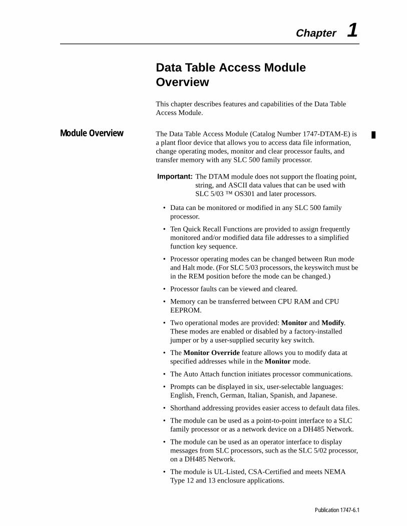
Chapter 1
Data Table Access Module Overview
This chapter describes features and capabilities of the Data Table Access Module.
Module Overview The Data Table Access Module (Catalog Number 1747-DTAM-E) is a plant floor device that allows you to access data file information, change operating modes, monitor and clear processor faults, and transfer memory with any SLC 500 family processor.
• Data can be monitored or modified in any SLC 500 family processor.
• Ten Quick Recall Functions are provided to assign frequentlymonitored and/or modified data file addresses to a simplified function key sequence.
• Processor operating modes can be changed between Run mand Halt mode. (For SLC 5/03 processors, the keyswitch musin the REM position before the mode can be changed.)
• Processor faults can be viewed and cleared.
• Memory can be transferred between CPU RAM and CPU EEPROM.
• Two operational modes are provided: Monitor and Modify. These modes are enabled or disabled by a factory-installed jumper or by a user-supplied security key switch.
• The Monitor Override feature allows you to modify data at specified addresses while in the Monitor mode.
• The Auto Attach function initiates processor communications
• Prompts can be displayed in six, user-selectable languages: English, French, German, Italian, Spanish, and Japanese.
• Shorthand addressing provides easier access to default data
• The module can be used as a point-to-point interface to a SLfamily processor or as a network device on a DH485 Network
• The module can be used as an operator interface to display messages from SLC processors, such as the SLC 5/02 proceon a DH485 Network.
• The module is UL-Listed, CSA-Certified and meets NEMA Type 12 and 13 enclosure applications.
Important: The DTAM module does not support the floating pointstring, and ASCII data values that can be used with SLC 5/03 ™ OS301 and later processors.
Publication 1747-6.1

1-2 Data Table Access Module Overview
tile
• Class I, Division 2, Groups A, B, C, D, Hazardous Location Certification
• A bi-color LED indicates operational mode and the status of certain fault and communication conditions.
• The keyboard is a 19-key, sealed membrane keypad with tacfeedback.
• The data display is a 16-character x 2-line, dot-matrix, backlitLCD with contrast control.
• A single cable is provided for power and communications.
• Module configuration parameters are stored in nonvolatile memory.
Publication 1747-6.1

in
,
ar-
or e
st
Chapter 2
Installation and Power Up
Read this chapter before installing the Data Table Access Module. It describes the procedures for:
• mounting the module
• connecting the module to your system
• module configuration and adjustments
• powering up the module
European Union Directive Compliance
If this product has the CE mark, it is approved for installation withthe European Union and EEA regions. It has been designed andtested to meet the following directives.
EMC Directive
This product is tested to meet Council Directive 89/336/EEC Electromagnetic Compatibility (EMC) and the following standardsin whole or in part, documented in a technical construction file:
• EN50081-2EMC – Generic Emission Standard, Part 2 – Industrial Environment
• EN50082-2EMC – Generic Immunity Standard, Part 2 – Industrial Environment
This product is intended for use in an industrial environment.
Mounting the Module The module is designed for mounting in a cutout on the door of anenclosure. The cutout and drilling dimensions for the module are shown on the following page. We have also included a full-size teout mounting template (appendix D) for your convenience.
When locating the cutout on the enclosure door:
• Provide 139.7 mm (5.5 in) clearance behind the enclosure doand 50.8 mm (2.0 in) electrical clearance above and below thmodule housing.
!ATTENTION: To keep the module temperature within the specified range, enclosure temperature mube between 0 to 55° (32 to 131° F).
Publication 1747-6.1

2-2 Installation and Power Up
re t
ss he
a
• Before drilling in the enclosure door, all power to the enclosumust be disconnected. Make sure the drill bit does not contacequipment and cause damage.
• Do not remove top label until after installation.
• A strain relief tab on the back of the module helps reduce streon the interconnect cable when the door is opened. Once themodule is installed, insert the cable under the tab and bend ttab downward to secure the cable.
• The module has a .8 Nm (7.0 in-lb) mounting torque.
• Insure that the module is grounded. If the DTAM is mounted tonon-conductive surface, attach a #8 AWG wire from the DTAMgrounding screw to the SLC chassis.
Prepare a cutout for your enclosure door using the measurementsshown below. See the template in Appendix D.
!ATTENTION: The module has ventilation holes on the top and bottom of the back cover. If you make additional holes in the enclosure, cover the module ventilation holes to protect against metal shavings entering the module housing.
104.8 mm(4.125 in.)
95.76 mm(3.77 in.)
Scrape paint to ensure good ground.
114.
3 m
m(4
.5 in
.)
128.
5 m
m(5
.06
in.)
Scrape paint to ensure good ground.
3.86 mm dia.(0.152 in.)4 holes
Publication 1747-6.1
Installation and Power Up 2-3
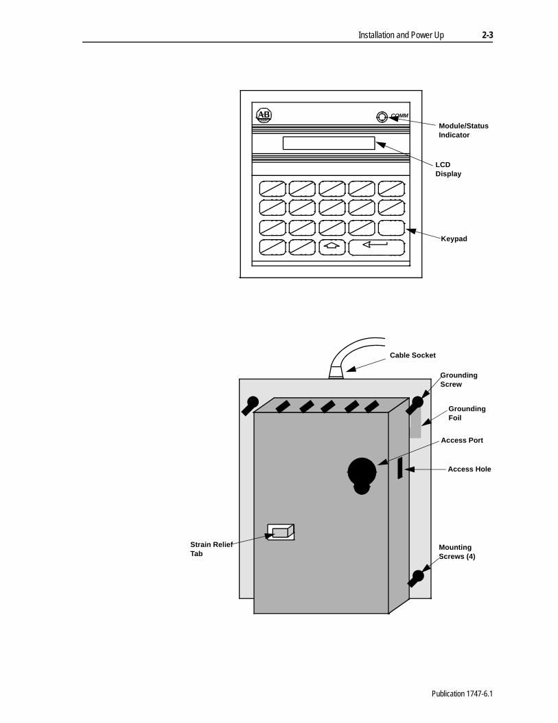
LCD Display
Module/Status Indicator
Keypad
COMM
Cable Socket
Grounding Screw
Grounding Foil
Access Port
Access Hole
Mounting Screws (4)
Strain Relief Tab
Publication 1747-6.1

2-4 Installation and Power Up
Connecting Your Equipment
Connect the module to your system as shown below:
Point-to-Point Connection to a SLC 500 Family Processor
Connection to a DH485 Network
DTAM
CH
Processor
Communications Port
Interconnect Cable1.8 m (6 ft.) 1747-C10
Link Coupler1747-AIC
DTAM
CH Peripheral
J2
Earth Ground
To Processor
To optional 24V dc Power Supply
Communication Cable
1747-C11
Interconnect Cable1.8 m (6 ft.) 1747-C10
Publication 1747-6.1
Installation and Power Up 2-5
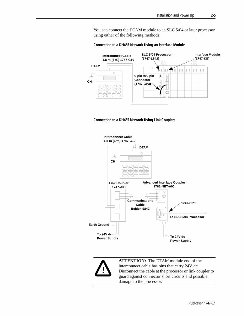
You can connect the DTAM module to an SLC 5/04 or later processor using either of the following methods.
Connection to a DH485 Network Using an Interface Module
Connection to a DH485 Network Using Link Couplers
DTAM
CH
Interconnect Cable1.8 m (6 ft.) 1747-C10
SLC 5/04 Processor(1747-L542)
Interface Module(1747-KE)
9-pin to 9-pin Connector(1747-CP3)
DTAM
CH
Interconnect Cable1.8 m (6 ft.) 1747-C10
Advanced Interface Coupler1761-NET-AIC
Link Coupler1747-AIC
Communications Cable
Belden 9842
Earth Ground
To 24V dc Power Supply
1747-CP3
To SLC 5/04 Processor
To 24V dc Power Supply
!ATTENTION: The DTAM module end of the interconnect cable has pins that carry 24V dc. Disconnect the cable at the processor or link coupler to guard against connector short circuits and possible damage to the processor.
Publication 1747-6.1

2-6 Installation and Power Up
to e
the he y
Module Configuration and Adjustments
The module’s access port and access hole allow you to adjust theLCD contrast and select the operational mode. Refer to chapter 5determine which mode to select, then return to this section to makthe physical setting.
The module is shipped from the factory with the jumper installed between terminals 1 and 2 to configure the module for the Modify operational mode.
To configure the module for the Monitor mode, either connect the jumper between terminals 1 and 3 (leaving the jumper installed inmodule) or completely remove the jumper. You may either leave theader in place and make the connection via the access port andaccess hole, or temporarily remove the header from the module bpulling it off of the plug. If you choose the latter method, return theheader to the plug once the connection is made.
3
2
1
Jumper
Header
PlugLCD Contrast Adjust Pot
Jumper
Access Hole ViewAccess Port View
3
2
1
Jumper
Header
PlugLCD Contrast Adjust Pot
Jumper
Access Hole ViewAccess Port View
Publication 1747-6.1

Installation and Power Up 2-7
The jumper may be removed and an externally mounted user-supplied key switch connected.
Modify Mode
Monitor Mode
Terminal 3 is unused.
LCD Contrast Adjust Pot
1.83 m (6 ft.)Maximum distance
Access Port View
!ATTENTION: To avoid damaging the module, when you wire an external keyswitch for mode control, use an isolated switching device. Do not apply power to the terminals.
ATTENTION: To avoid damaging the module, when you change the mode select jumper, disconnect power from the module. Move the top lead of the jumper between terminals 2 and 3. Always leave the lead attached to the bottom terminal (terminal 1) connected.
Important: After you have set up the module for your application, to prevent unauthorized access to data files, connect the jumper for the Monitor mode or wire the key switch as shown .
Publication 1747-6.1

2-8 Installation and Power Up
,
pter
Power-Up Sequence When the module is plugged into a processor or link coupler for the first time, the following sequence occurs:
1. The Communications LED illuminates solid red.
2. The module performs diagnostic self tests.
3. When the tests are complete, the Communications LED turns off, and the LCD displays:
If the module fails any of the self diagnostic tests, refer to chapter 9, Troubleshooting, for a list of error and fault codes.
4. The Communications LED flashes green, and the LCD displays:
5. After a successful power-up, the display shows the ready prompt. You can now perform any of the following functions:
• Change the Module Setup. Refer to chapter 3, Module Setup Procedure.
• Initiate communications with a SLC 500 family processor. Refer to chapter 4, Attaching to a Processor.
• Clear an existing Quick Recall Function. Refer to chapter 6Quick Recall Functions.
• Observe and respond to a displayed message. Refer to cha8, Message Capability.
Enter NetworkWorking . . .
RDY>
Publication 1747-6.1
ns
Chapter 3
Module Setup Procedure
This chapter describes the setup procedures for configuring the operation of the module for specific applications. The topics covered are:
• language for the module display
• module node address
• module baud rate
• Auto Attach function
• LCD backlighting
• Monitor Override function
• module reset function
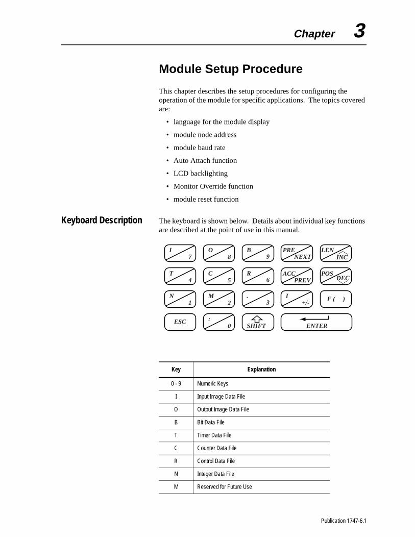
Keyboard Description The keyboard is shown below. Details about individual key functioare described at the point of use in this manual.
ENTERSHIFTESC
I O B PRE LEN7 8 9 NEXT INC
ACC POSPREV DEC
T C R4 5 6
N M . I1 2 3
:0
+/-F ( )
Key Explanation
0 - 9 Numeric Keys
I Input Image Data File
O Output Image Data File
B Bit Data File
T Timer Data File
C Counter Data File
R Control Data File
N Integer Data File
M Reserved for Future Use
Publication 1747-6.1

3-2 Module Setup Procedure
Factory Default Settings
The module is shipped from the factory with the following default settings:
Key Explanation
: Data File Addressing Element Delimiter
. Data File Addressing Word Delimiter
/ Data File Addressing Bit Delimiter
PRE Timer/Counter Preset Word
ACC Timer/Counter Accumulator Word
LEN Control Register File Length Word
POS Control Register Pointer Position Word
+/- Positive/Negative Signed Integer
NEXT Increment to Next Logical Address
PREV Decrement to Previous Logical Address
INC Increment Data Value or Control Bit
DEC Decrement Data Value or Control Bit
F( ) Function Key
ESC Escape Key
SHIFT Shift to Upper Case
ENTER Enter Desired Parameter
Feature Default Setting
Language English
DTAM Node Address 0
Baud Rate 19200
Auto Attach Off
LCD Backlighting On
Monitor Override Off
Publication 1747-6.1
Module Setup Procedure 3-3
D
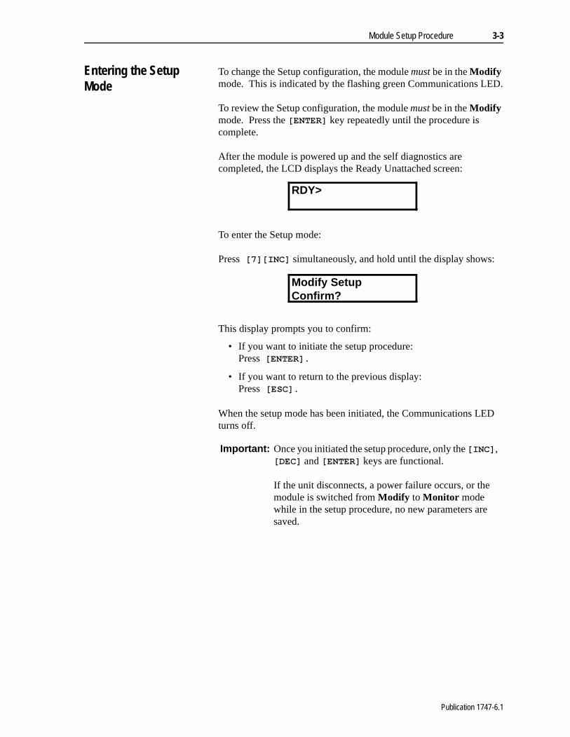
Entering the Setup Mode
To change the Setup configuration, the module must be in the Modify mode. This is indicated by the flashing green Communications LED.
To review the Setup configuration, the module must be in the Modify mode. Press the >(17(5@ key repeatedly until the procedure is complete.
After the module is powered up and the self diagnostics are completed, the LCD displays the Ready Unattached screen:
To enter the Setup mode:
Press�>�@>,1&@ simultaneously, and hold until the display shows:
This display prompts you to confirm:
• If you want to initiate the setup procedure:Press >(17(5@�
• If you want to return to the previous display:Press�>(6&@�
When the setup mode has been initiated, the Communications LEturns off.
RDY>
Modify SetupConfirm?
Important: Once you initiated the setup procedure, only the >,1&@,�>'(&@ and >(17(5@ keys are functional.
If the unit disconnects, a power failure occurs, or the module is switched from Modify to Monitor mode while in the setup procedure, no new parameters aresaved.
Publication 1747-6.1
3-4 Module Setup Procedure
ns to
gh
Do
Selecting the Language
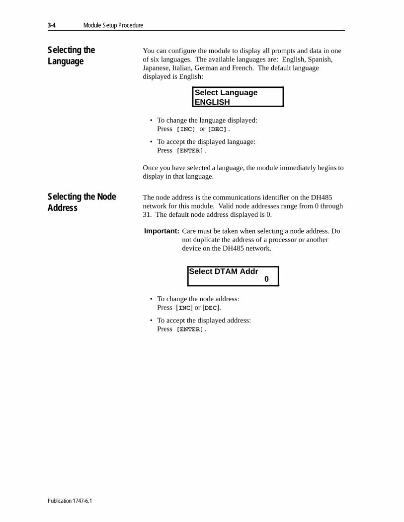
You can configure the module to display all prompts and data in one of six languages. The available languages are: English, Spanish, Japanese, Italian, German and French. The default language displayed is English:
• To change the language displayed:Press >,1&@ or >'(&@�
• To accept the displayed language:Press >(17(5@�
Once you have selected a language, the module immediately begidisplay in that language.
Selecting the Node Address
The node address is the communications identifier on the DH485network for this module. Valid node addresses range from 0 throu31. The default node address displayed is 0.
• To change the node address:Press [,1&] or ['(&].
• To accept the displayed address:Press >(17(5@�
Select LanguageENGLISH
Important: Care must be taken when selecting a node address. not duplicate the address of a processor or another device on the DH485 network.
Select DTAM Addr0
Publication 1747-6.1

Module Setup Procedure 3-5
r.
o
Setting the Baud Rate This is the communications rate for the module. Available baud rates are: 1200, 2400, 9600 and 19200 baud. The default baud rate displayed is 19200.
• To scroll through the available baud rates:Press [,1&] or ['(&].
• To accept the displayed baud rate:Press [(17(5].
Setting the Auto Attach Function
This selection determines how the module attaches to a processoThe default selection is Off.
When the function is set to Off, you are required to manually attach ta processor each time the module is powered up.
When the function is set to On, the module attempts to attach to theaddress of the last processor it was logically attached to or to thedefault node address of one.
• To toggle between On and Off:Press [,1&] or ['(&].
• To accept the setting:Press [(17(5].
Important: All devices on the DH485 network, including the module, must be set to the same baud rate.
Select Baud Rate19200
Set Auto AttachOFF
Publication 1747-6.1
3-6 Module Setup Procedure
file
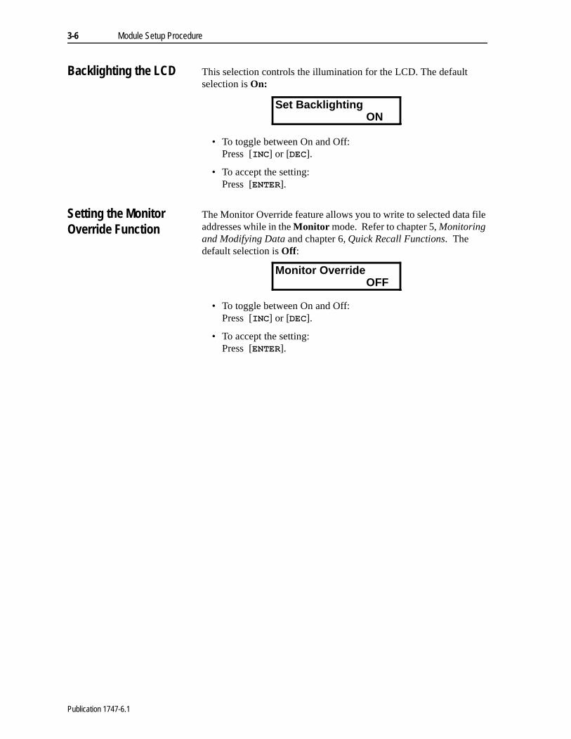
Backlighting the LCD This selection controls the illumination for the LCD. The default selection is On:
• To toggle between On and Off:Press [,1&] or ['(&].
• To accept the setting:Press [(17(5].
Setting the Monitor Override Function
The Monitor Override feature allows you to write to selected data addresses while in the Monitor mode. Refer to chapter 5, Monitoring and Modifying Data and chapter 6, Quick Recall Functions. The default selection is Off:
• To toggle between On and Off:Press [,1&] or ['(&].
• To accept the setting:Press [(17(5].
Set BacklightingON
Monitor OverrideOFF
Publication 1747-6.1
Module Setup Procedure 3-7
he
, the
g tion
re e
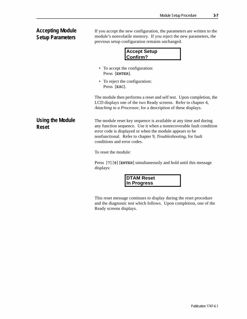
Accepting Module Setup Parameters
If you accept the new configuration, the parameters are written to the module’s nonvolatile memory. If you reject the new parameters, tprevious setup configuration remains unchanged.
• To accept the configuration:Press [(17(5].
• To reject the configuration:Press [(6&].
The module then performs a reset and self test. Upon completionLCD displays one of the two Ready screens. Refer to chapter 4, Attaching to a Processor, for a description of these displays.
Using the Module Reset
The module reset key sequence is available at any time and durinany function sequence. Use it when a nonrecoverable fault condierror code is displayed or when the module appears to be nonfunctional. Refer to chapter 9, Troubleshooting, for fault conditions and error codes.
To reset the module:
Press [�] [�] [(17(5] simultaneously and hold until this message displays:
This reset message continues to display during the reset proceduand the diagnostic test which follows. Upon completion, one of thReady screens displays.
Accept SetupConfirm?
DTAM ResetIn Progress
Publication 1747-6.1

3-8 Module Setup Procedure
Publication 1747-6.1

tiate
n:
e a
lay d to - the
Chapter 4
Attaching to a Processor
Read this chapter before initiating communications between the module and a SLC 500 family processor. It describes:
• Manual Attach procedure
• Auto Attach procedure
• Ready Attached screen
• Backspace Function during attach procedure
• attaching to a password-protected processor
Manual Attach Procedure
After the module is powered up and the setup parameters are configured, you are ready to attach to the desired processor to inicommunications.
You may perform the attach procedure with the module in either Monitor or Modify mode. Refer to chapter 5, Monitoring and Modifying Data, for descriptions of these modes.
If the module is configured with the Auto Attach feature set to Off:
1. At power up, the display shows the Ready Unattached scree
2. To attach to a processor node address:Press [)��] [6+,)7].
3. Notice the symbol to the right of RDY has changed to indicatshifted key function:
4. To Continue:Press [,].
5. The module displays the attach to CPU screen. Asterisks dispin the lower right-hand corner if the module was not previouslyattached to a processor or if the last processor it was attacheis no longer active. If a number is displayed in the lower righthand corner, it is the node address of the processor to whichmodule was previously attached.
RDY>
RDY^
Attach to CPU? **
Publication 1747-6.1

4-2 Attaching to a Processor
the
to
y
f the ows:
to
6. To change the node address:
• Scroll through the list of active node addresses attached tonetwork. Press [,1&] or ['(&].
• Use the numeric keys to enter a value from 0 through 31.
7. Once the appropriate node address is displayed:Press [(17(5].
8. The module displays the Ready Attached screen:
If the processor you are attaching to is password-protected, refer the section on attaching to a password-protected processor on page 4-4.
Auto Attach Procedure If the module is configured with the Auto Attach feature set to On:
1. At power up, the module displays:
2. When the module completes the attach procedure, the displashows the Ready Attached screen:
If the module has not been previously attached to a processor or ilast processor it was attached to is no longer active, the display sh
1. To change the node address:
• Press [,1&] or ['(&] to scroll through the list of active node addresses attached to the network.
• Use the numeric keys to enter a value from 0 through 31.
2. Once the appropriate node address is displayed:Press [(17(5].
If the processor you are attaching to is password-protected, refer the section on attaching to a password-protected processor on page 4-4.
RDY> 4 RRUN5/02 4444
Attach to CPU?WORKING . . . .
RDY> 4 RRUN5/02 4444
Attach to CPU? **
Publication 1747-6.1

Attaching to a Processor 4-3
elow.
Ready Attached Screen
The Ready Attached screen displays the ready prompt, processor node address, and processor operating mode on the top line, and the processor type and program name on the bottom line:
Operating Mode Text
The text displayed in the Ready Attached screen depends on the processor mode and type, as summarized in the table below.
Backspace Function During Attach Procedure
If you incorrectly entered the node address during the Attach procedure (and have not pressed [(17(5] yet), you can use the Backspace Function to delete characters from right to left, and then re-type the value. Backspacing to the beginning of the string (leftmost character) will in most cases return the default value. The exception is during password entry.
There are two ways to implement the Backspace Function:
• Single Backspace - Press and release the [6+,)7] key, then press and release the [(6&] key.
• Multiple Backspace - Press and hold the [6+,)7] key while repeatedly pressing the [(6&] key.
The example below shows a default node address of 15.
If you press 3 then 0, the node address changes to 30, as shown b
RDY> 4 RRUN5/02 4444
Processor Mode Operating Mode Text
SLC 500, SLC 5/01™ and
SLC 5/02™ Processorsand
SLC 5/03 and SLC 5/04 processors with
Keyswitch in REM
SLC 5/03 or later processors with Keyswitch
Not in REM
Run RRUN RUN
Program RHALT HALT
Test RTEST HALT
Fault FAULT FAULT
Attach to CPU?15
Attach to CPU?30
Publication 1747-6.1
4-4 Attaching to a Processor
ter 8,
is
If you press and release the [6+,)7] key, then press and release the [(6&] key, the display appears as:
To restore the default value of 15, press and release the [6+,)7] key, then press and release the [(6&] key.
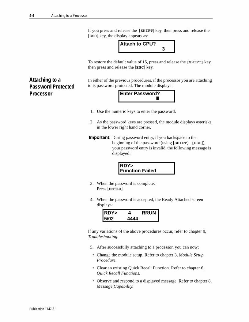
Attaching to a Password Protected Processor
In either of the previous procedures, if the processor you are attaching to is password-protected. The module displays:
1. Use the numeric keys to enter the password.
2. As the password keys are pressed, the module displays asterisks in the lower right hand corner.
3. When the password is complete:Press [(17(5].
4. When the password is accepted, the Ready Attached screen displays:
If any variations of the above procedures occur, refer to chapter 9, Troubleshooting.
5. After successfully attaching to a processor, you can now:
• Change the module setup. Refer to chapter 3, Module Setup Procedure.
• Clear an existing Quick Recall Function. Refer to chapter 6, Quick Recall Functions.
• Observe and respond to a displayed message. Refer to chapMessage Capability.
Attach to CPU?3
Enter Password?
Important: During password entry, if you backspace to the beginning of the password (using [6+,)7@�>(6&]), your password entry is invalid. the following message displayed:
RDY>Function Failed
RDY> 4 RRUN5/02 4444
Publication 1747-6.1
ule.
of
ta r 3 this
Chapter 5
Monitoring and Modifying Data
This chapter describes:
• operating modes
• logical data file addressing
• Backspace Function during data file address entry
• quick access addressing
• entering data file addresses
• changing displayed data file addresses
• changing data file values
Operating Modes The module has two operational modes, Modify and Monitor. A Monitor Override feature is also provided.
Modify Mode
The module is shipped from the factory configured for the Modify mode. This mode allows access to all features available in the modRefer to chapter 2, Installation and Power Up, for details on the Modify mode configuration.
Monitor Mode
When the module is configured for the Monitor mode, you are allowed to display values contained in data file words. Alteration data within the processor data files is prohibited. This mode of operation is provided to prevent unauthorized access to certain processor functions. Refer to chapter 2, Installation and Power Up, for details on configuring the unit for the Monitor mode.
Monitor Override Feature
When configured for the Monitor mode, a Monitor Override feature is provided to allow data modification of up to ten user-defined dafile addresses using the Quick Recall Functions. Refer to chaptefor details on how to use the module setup procedure to configurefeature. Refer to chapter 6 for a description of the Quick Recall Functions.
Publication 1747-6.1

5-2 Monitoring and Modifying Data
See the chart below for the functions you may perform in each mode:
The communications LED on the module changes according to the operational mode selected, as shown below:
For additional information regarding the LED functions, refer to chapter 9, Troubleshooting.
Operation Monitor Mode Modify Mode
Module Setup No Yes
Monitor Data File Address Yes Yes
Modify Data File Address No1 Yes2
Change Processor Mode No Yes
Transfer EEPROM Memory to RAM No Yes
Transfer RAM Memory to EEPROM No Yes
Define a Quick Recall Function No Yes
Recall a Quick Recall Function Yes Yes
Clear a Quick Recall Function No Yes
Attach to a Processor Yes Yes
View a Processor Fault Yes Yes
Clear a Processor Fault No Yes
Receive a Message Yes Yes
Respond to a Message Yes Yes
1. Up to 10 user-defined addresses may be modified using the Monitor Override feature.
2. Input and Output Image Table words are always view only. In 5/02 and 5/03 processors, data files may have additional file protection preventing the DTAM from changing data.
LED DTAM Operating Mode
Flashing Green Modify Mode
Flashing Green Data being entered using the Monitor Override feature
Solid Green Monitor Mode
Publication 1747-6.1
Monitoring and Modifying Data 5-3
Logical Data File Addressing
SLC 500 family logical addressing can be used with the module to access all data files except the status file (S2). You may access any valid address in the attached processor.
1. For example, to access T10:100.ACC you would use the following key sequence:Press >6+,)7@��>7@��>�@��>�@��>6+,)7@��>�@��>�@>�@��>�@��>$&&@�>(17(5@�As the address is being entered, the address will be displayed inthe lower left-hand corner of the LCD.
2. When the [(17(5] key is pressed, the display shows the logical address on the top line and its associated value in the lower right-hand corner:
1. To logically address to the bit level for B3:2/9, use the following key sequence:Press >6+,)7@� � >%@� � >�@� � >6+,)7@� � >�@� � >�@>6+,)7@��>�@��>�@��>(17(5@�
2. The LCD displays the logical address on the top line and the on/off status of that bit on the bottom line:
For more information on logical addressing, see appendix B.
T10:100.ACC999
Important: Once you press [6+,)7] [7], [&] or [5], it is not necessary to press the [6+,)7] key for [35(], [$&&], [/(1] or [326].
B3:2/9. . . . . . . 0 . . . . . . . . . . . .
Publication 1747-6.1

5-4 Monitoring and Modifying Data
ht. r
Backspace Function During Data File Address Entry
If you made an error while entering a data file address (and have not pressed [(17(5] yet), you can use the Backspace Function to delete characters and re-type the address.
The following strings are deleted in one keystroke:
• .ACC
• .LEN
• .POS
• .PRE
When you enter data table addresses, text entry is from left to rigIn the example below, T255:7.PRE has just been entered. The cursois to the right of PRE.
If you press and release the [6+,)7] key, and then press and releasethe [(6&] key, the display appears as:
Backspacing over the first character that you entered returns the information previously displayed on line two.
RDY> 4 RRUNT255:7.PRE
RDY> 4 RRUNT255:7
Publication 1747-6.1
Monitoring and Modifying Data 5-5
Quick Access Addressing
The module provides you with a shorthand method of data file addressing for default files 3 through 7. Type the file identifier: %��7��&��5�or 1� then [(17(5]. The module displays the first address within that file.
1. For example, to display the first address in the Integer file:Press��>6+,)7@�>1@�>(17(5@�The module displays:
2. You can now use the [1(;7] and [35(9] keys to step through all the addresses contained in that file. This is explained later in this chapter.
You may also access a specific element within a data file.
1. To display the Input Image Table word for slot 2:Press >6+,)7@�>,@�>�@�>(17(5@�
2. The module displays the logical address on the top and the on/off status of each of the bits associated with that word on the bottom line:
N7:0123
I1:2.0 0000111100110101
Important: Input and Output Image Table words can only be monitored. The Input Image data file represents external input conditions and cannot be modified by the module. The Output Image data file is controlled by the user program and cannot be modified by the module.
Publication 1747-6.1

5-6 Monitoring and Modifying Data
You may use shorthand addressing to display an address at the bit level.
1. To display the on/off status of the bit B3:1/14:Press >6+,)7@�>%@�>6+,)7@�>�@�>�@�>�@�>(17(5@�The display shows the logical address on the top line and the on/off status of that bit on the bottom line:
2. You can now use the [,1&] and ['(&] keys to step through each bit in that word. This is explained later in this chapter.
The following chart shows you how shorthand addressing corresponds to the logical addresses in processor memory:
Data File addresses may be entered from any Attached display except the Data Entry display, described later in this chapter.
B3:1/14 . 1 . . . . . . . . . . . . . . . . .
Keyboard Entry Data File Address
O0 to O31 O0:0.0 to O0:31.0
I0 to I31 I1:0.0 to I1:31.0
B0 to B255 B3:0 to B3:255
T0 to T255 T4:0 to T4:255
T0.PRE to T255.PRE T4:0.PRE to T4:255.PRE
T0.ACC to T255.ACC T4:0.ACC to T4:255.ACC
C0 to C255 C5:0 to C5:255
C0.PRE to C255.PRE C5:0.PRE to C5:255.PRE
C0.ACC to C255.ACC C5:0.ACC to C5:255.ACC
R0 to R255 R6:0 to R6:255
R0.POS to R255.POS R6:0.POS to R6:255.POS
R0.LEN to R255.LEN R6:0.LEN to R6:255.LEN
N0 to N255 N7:0 to N7:255
Publication 1747-6.1

Monitoring and Modifying Data 5-7
Entering Data File Addresses
The following flowchart shows you the variations available for entering data file addresses:
Entering Input and Output Addresses
Entering Bit Addresses
Entering Timer and Counter Addresses
2
,
Q
QQ ��� �
� �
(17(5
����
����� ����
�
%
Q
Q�
Q�Q
(17(5
��������������
�������
����
7
&
Q
Q
35(
$&&
�
Q �
Q �
(17(5
��������������
��������� 7������&������
Publication 1747-6.1
5-8 Monitoring and Modifying Data
Entering Control Register Addresses
Entering Integer Addresses
5
Q
Q
/(1
326
�
Q �
(17(5
��������������
����������
1
QQ �
(17(5
��������� �����
Publication 1747-6.1
Monitoring and Modifying Data 5-9
ated
ated
e of
ords t.
How to Change Displayed Data File Addresses
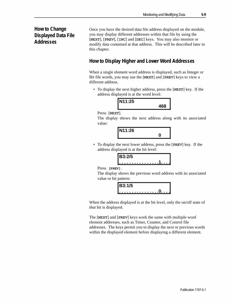
Once you have the desired data file address displayed on the module, you may display different addresses within that file by using the [1(;7], [35(9], [,1&] and ['(&] keys. You may also monitor or modify data contained at that address. This will be described later in this chapter.
How to Display Higher and Lower Word Addresses
When a single element word address is displayed, such as Integer or Bit file words, you may use the [1(;7] and [35(9] keys to view a different address.
• To display the next higher address, press the [1(;7] key. If the address displayed is at the word level:
Press [1(;7].The display shows the next address along with its associvalue:
• To display the next lower address, press the [35(9] key. If the address displayed is at the bit level:
Press [PREV].The display shows the previous word address with its associvalue or bit pattern:
When the address displayed is at the bit level, only the on/off statthat bit is displayed.
The [1(;7] and [35(9] keys work the same with multiple word element addresses, such as Timer, Counter, and Control file addresses. The keys permit you to display the next or previous wwithin the displayed element before displaying a different elemen
N11:25468
N11:260
B3:2/5. . . . . . . . . . . . . . . .1. . . .
B3:1/5. . . . . . . . . . . . . . . .0. . . .
Publication 1747-6.1
5-10 Monitoring and Modifying Data
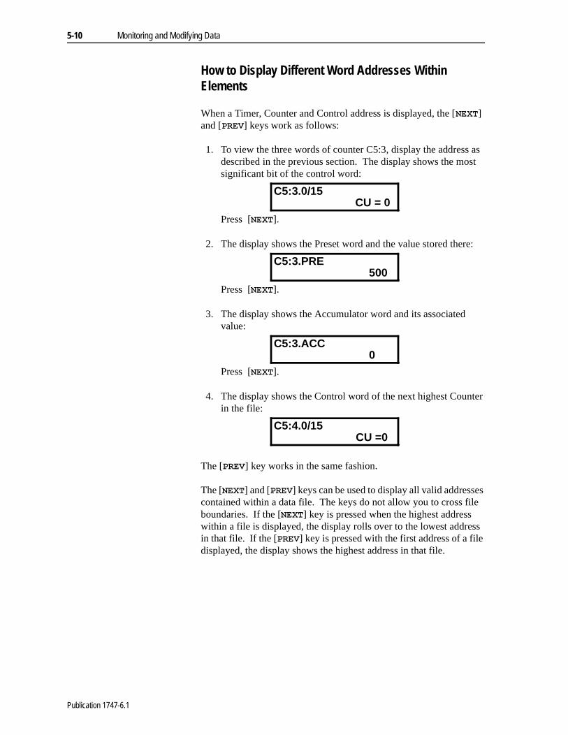
How to Display Different Word Addresses Within Elements
When a Timer, Counter and Control address is displayed, the [1(;7] and [35(9] keys work as follows:
1. To view the three words of counter C5:3, display the address as described in the previous section. The display shows the most significant bit of the control word:
Press [1(;7].
2. The display shows the Preset word and the value stored there:
Press [1(;7].
3. The display shows the Accumulator word and its associated value:
Press [1(;7].
4. The display shows the Control word of the next highest Counter in the file:
The [35(9] key works in the same fashion.
The [1(;7] and [35(9] keys can be used to display all valid addresses contained within a data file. The keys do not allow you to cross file boundaries. If the [1(;7] key is pressed when the highest address within a file is displayed, the display rolls over to the lowest address in that file. If the [35(9] key is pressed with the first address of a file displayed, the display shows the highest address in that file.
C5:3.0/15CU = 0
C5:3.PRE500
C5:3.ACC0
C5:4.0/15CU =0
Publication 1747-6.1
Monitoring and Modifying Data 5-11
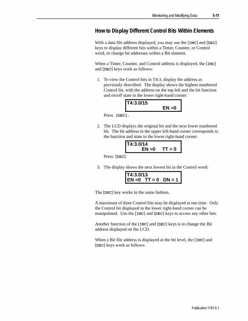
How to Display Different Control Bits Within Elements
With a data file address displayed, you may use the [,1&] and ['(&] keys to display different bits within a Timer, Counter, or Control word, or change bit addresses within a Bit element.
When a Timer, Counter, and Control address is displayed, the [,1&] and ['(&] keys work as follows:
1. To view the Control bits in T4:3, display the address as previously described. The display shows the highest numbered Control bit, with the address on the top left and the bit function and on/off state in the lower right-hand corner:
Press >'(&@�
2. The LCD displays the original bit and the next lower numbered bit. The bit address in the upper left-hand corner corresponds to the function and state in the lower right-hand corner:
Press ['(&].
3. The display shows the next lowest bit in the Control word:
The ['(&] key works in the same fashion.
A maximum of three Control bits may be displayed at one time. Only the Control bit displayed in the lower right-hand corner can be manipulated. Use the [,1&] and ['(&] keys to access any other bits.
Another function of the [,1&] and ['(&] keys is to change the Bit address displayed on the LCD.
When a Bit file address is displayed at the bit level, the [,1&] and ['(&] keys work as follows:
T4:3.0/15EN =0
T4:3.0/14EN =0 TT = 0
T4:3.0/13EN =0 TT = 0 DN = 1
Publication 1747-6.1
5-12 Monitoring and Modifying Data
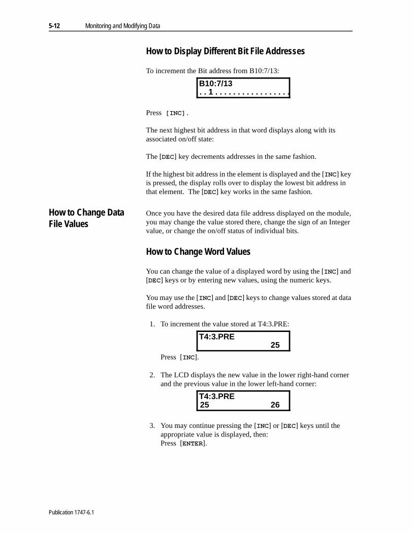
How to Display Different Bit File Addresses
To increment the Bit address from B10:7/13:
Press >,1&@�
The next highest bit address in that word displays along with its associated on/off state:
The ['(&] key decrements addresses in the same fashion.
If the highest bit address in the element is displayed and the [,1&] key is pressed, the display rolls over to display the lowest bit address in that element. The ['(&] key works in the same fashion.
How to Change Data File Values
Once you have the desired data file address displayed on the module, you may change the value stored there, change the sign of an Integer value, or change the on/off status of individual bits.
How to Change Word Values
You can change the value of a displayed word by using the [,1&] and ['(&] keys or by entering new values, using the numeric keys.
You may use the [,1&] and ['(&] keys to change values stored at data file word addresses.
1. To increment the value stored at T4:3.PRE:
Press [,1&].
2. The LCD displays the new value in the lower right-hand corner and the previous value in the lower left-hand corner:
3. You may continue pressing the [,1&] or ['(&] keys until the appropriate value is displayed, then:Press [(17(5].
B10:7/13. . 1 . . . . . . . . . . . . . . . . .
T4:3.PRE25
T4:3.PRE2625
Publication 1747-6.1

Monitoring and Modifying Data 5-13
4. The address displays with the new value in the lower right-hand corner:
When pressing these keys, the longer you hold the key, the faster the values change.
When you use the [,1&] and ['(&] keys, the module display automatically rolls over or under the value when the numeric high or low limit of the data file is reached. The following table lists the values for the different files:
You may also use the numeric keys to enter or change a value at a displayed address.
• To enter the value 567 into T4:5.PRE:
Press >�@�>�@�>�@�>(17(5@�The address and the new value displays:
T4:3.PRE26
Data File Roll Over/Under Range
Timer PRE and ACCRoll over at 32767 to 0
Roll under at 0 to 32767
Counter PRE and ACCRoll over at 32767 to –32768
Roll under at –32768 to 32767
Control LEN and POS Roll over at 32767 to 0Roll under at 0 to 32767
IntegerRoll over at 32767 to –32768
Roll under at –32768 to 32767
T4:5 PRE0
T4:5 PRE567
Important: Once data entry has been initiated, you may not attempt to display different addresses. You must either finish the data entry and press [(17(5] or press [(6&].
Once data entry has been initiated, if you press the [(6&] key or switch the module from Modify to Monitor mode, the new value is lost.
Publication 1747-6.1

5-14 Monitoring and Modifying Data
6
t te alue
The
t
How to Change the Sign of a Value
The [���] key may be used to change the sign of signed integers contained in the Counter or Integer data files.
• For example, to change the sign of the signed integer value 5stored at word N20:7:
Press �>�@�>���@�>�@�>(17(5@�The module displays:
Backspace Function During Data File Value Entry
If you make an error while entering a data file value (and have nopressed [(17(5] yet), you can use the Backspace Function to delecharacters and re-type the value. In the example below, integer v56 has just been entered.
The cursor is positioned to the right of the 6.
If you press and release the [6+,)7] key, then press and release the[(6&] key, the display appears as:
Backspacing over the first character abandons the integer entry. module then returns to monitoring the data file address and the original data value.
N20:756
N20:7-56
Important: To enter a negative number into an address, you musenter at least one numeric value before pressing the [���] key.
N20:756789
N20:75789
Publication 1747-6.1
Monitoring and Modifying Data 5-15
was
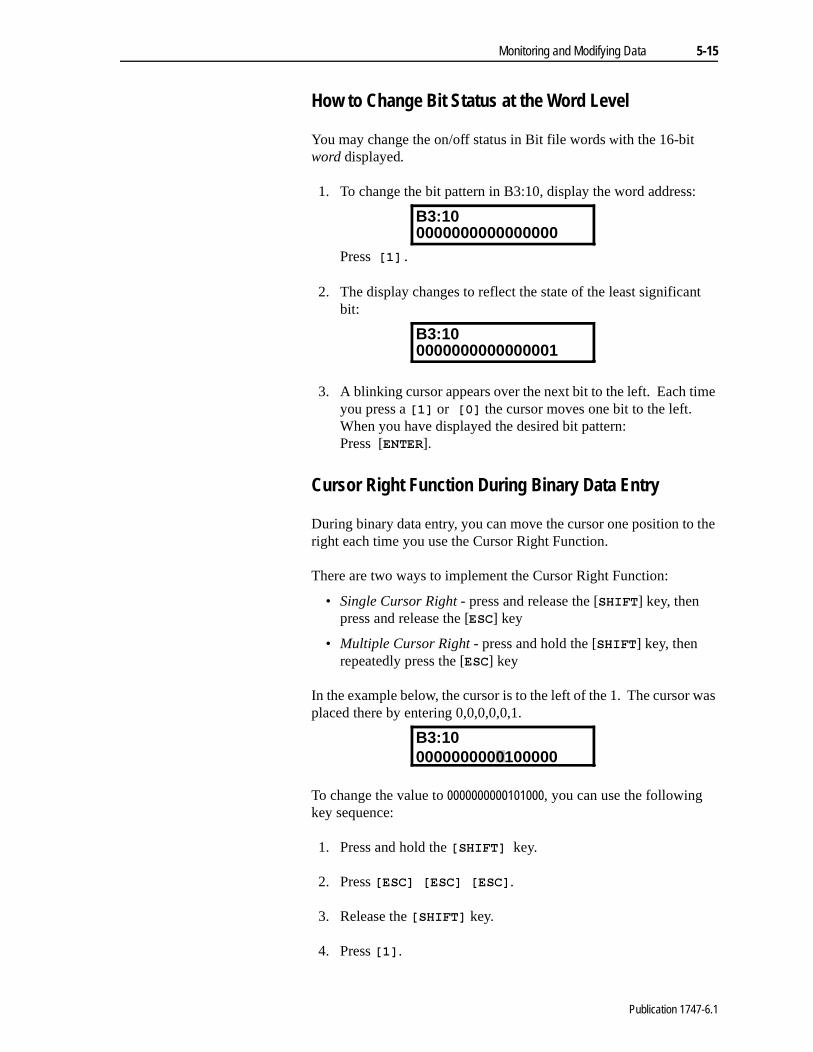
How to Change Bit Status at the Word Level
You may change the on/off status in Bit file words with the 16-bit word displayed.
1. To change the bit pattern in B3:10, display the word address:
Press >�@�
2. The display changes to reflect the state of the least significant bit:
3. A blinking cursor appears over the next bit to the left. Each time you press a >�@ or�>�@ the cursor moves one bit to the left. When you have displayed the desired bit pattern:Press [(17(5].
Cursor Right Function During Binary Data Entry
During binary data entry, you can move the cursor one position to the right each time you use the Cursor Right Function.
There are two ways to implement the Cursor Right Function:
• Single Cursor Right - press and release the [6+,)7] key, then press and release the [(6&] key
• Multiple Cursor Right - press and hold the [6+,)7] key, then repeatedly press the [(6&] key
In the example below, the cursor is to the left of the 1. The cursor placed there by entering 0,0,0,0,0,1.
To change the value to 0000000000101000, you can use the following key sequence:
1. Press and hold the >6+,)7@ key.
2. Press >(6&@�>(6&@�>(6&@.
3. Release the >6+,)7@ key.
4. Press >�@.
B3:100000000000000000
B3:100000000000000001
B3:100000000000100000
Publication 1747-6.1
5-16 Monitoring and Modifying Data
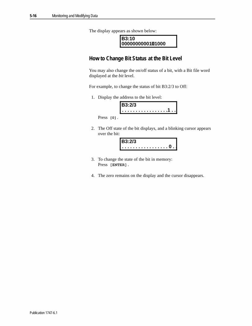
The display appears as shown below:
How to Change Bit Status at the Bit Level
You may also change the on/off status of a bit, with a Bit file word displayed at the bit level.
For example, to change the status of bit B3:2/3 to Off:
1. Display the address to the bit level:
Press [0].
2. The Off state of the bit displays, and a blinking cursor appears over the bit:
3. To change the state of the bit in memory:Press >(17(5@�
4. The zero remains on the display and the cursor disappears.
0000000000101000B3:10
B3:2/3. . . . . . . . . . . . . . . . .1 . .
B3:2/3. . . . . . . . . . . . . . . . . 0 . .
Publication 1747-6.1

ata the You sing
e
he
Chapter 6
Quick Recall Functions
This chapter describes how to:
• define Quick Recall Functions
• use Quick Recall Functions
• clear Quick Recall Functions
Quick Recall Function Overview
The module has the capability to let you define and use up to 10 dfile address Quick Recall Functions. These functions are stored inmodule’s nonvolatile memory. They allow you to assign frequentlyaccessed data file addresses to a simplified keystroke procedure.may later recall these addresses by pressing two keys instead of uthe addressing procedure described in the previous chapter.
Quick Recall Functions also provide the ability to write data to selected data file addresses when the module is configured for thMonitor mode. This Monitor Override feature is enabled in the Module Setup Procedure described in chapter 3.
Defining Quick Recall Functions
The available Quick Recall Functions are numbered F(0) throughF(9). For example, to assign address T4:1.ACC to Quick Recall Function F(1):
1. Configure the module for the Modify mode.
2. Make sure the module is attached to a processor.
3. Enter the data file address:Press >6+,)7@�>7@�>�@�>$&&@�>(17(5@�
4. The address and its current value are displayed:
5. To define Quick Recall Function F(1):Press >6+,)7@�>)��@�>)��@�>�@�>(17(5@�
6. The Quick Recall Function for that address is now stored in tmodule nonvolatile memory. The display shows the followingfor three seconds:
T4:1.ACC9999
Macro 1 DefinedT4:1.ACC
Publication 1747-6.1

6-2 Quick Recall Functions
le
7. The display then returns to the previous address display:
8. You may now perform any of the module functions.
Using Quick Recall Functions
After defining the Quick Recall Function, you are able to recall that data file address at any time. The module may be configured for the Modify or Monitor modes.
In the Monitor mode, if the unit has been configured with the Monitor Override feature set to On, you can modify data at that data file address by recalling the Quick Recall Function.
1. Make sure the module is attached to a processor.
2. To recall Quick Recall Function F(1), from any screen:Press >)��@�>�@�
3. The module displays the data file address assigned to that Quick Recall Function:
4. You are now able to view or alter the data at this data file address using the procedures described in the previous chapter.
T4:1.ACC9999
Important: If the unit is connected to a DH485 Network, the module is able to communicate with multiple processors on the network. Any data file address assigned to a Quick Recall Function and stored in the module’s nonvolatile memory is accessible in any processor data file on the network to which the moduis attached.
Important: Data can be modified in the Monitor mode with the Monitor Override set to On only at the address displayed by a Quick Recall Function. Addresses displayed using the >1(;7@��>35(9@��>,1&@ or >'(&@ keys can be monitored but not modified in thismode.
T4:1.ACC9999
Publication 1747-6.1
Quick Recall Functions 6-3
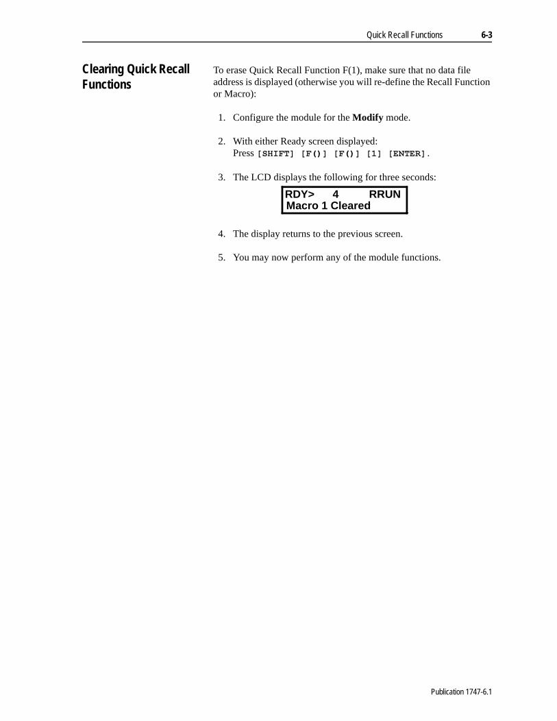
Clearing Quick Recall Functions
To erase Quick Recall Function F(1), make sure that no data file address is displayed (otherwise you will re-define the Recall Function or Macro):
1. Configure the module for the Modify mode.
2. With either Ready screen displayed:Press >6+,)7@�>)��@�>)��@�>�@�>(17(5@.
3. The LCD displays the following for three seconds:
4. The display returns to the previous screen.
5. You may now perform any of the module functions.
RDY> 4 RRUNMacro 1 Cleared
Publication 1747-6.1

6-4 Quick Recall Functions
Publication 1747-6.1
e ssor,
the yed
:
Chapter 7
Processor Control Functions
This chapter describes the procedures to:
• change processor modes
• view and clear processor faults
• transfer user programs between RAM and EEPROM memory
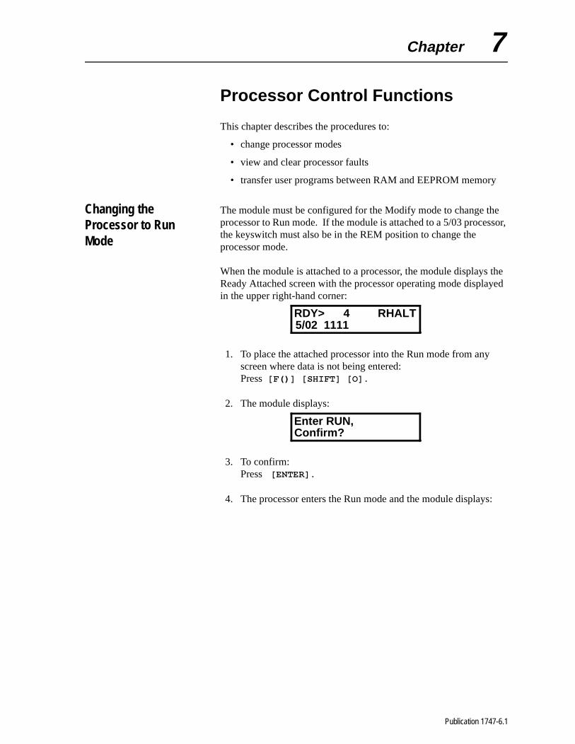
Changing the Processor to Run Mode
The module must be configured for the Modify mode to change thprocessor to Run mode. If the module is attached to a 5/03 procethe keyswitch must also be in the REM position to change the processor mode.
When the module is attached to a processor, the module displaysReady Attached screen with the processor operating mode displain the upper right-hand corner:
1. To place the attached processor into the Run mode from anyscreen where data is not being entered:Press >)��@�>6+,)7@�>2@�
2. The module displays:
3. To confirm:Press �>(17(5@�
4. The processor enters the Run mode and the module displays
RDY> 4 RHALT5/02 1111
Confirm?Enter RUN,
Publication 1747-6.1
7-2 Processor Control Functions
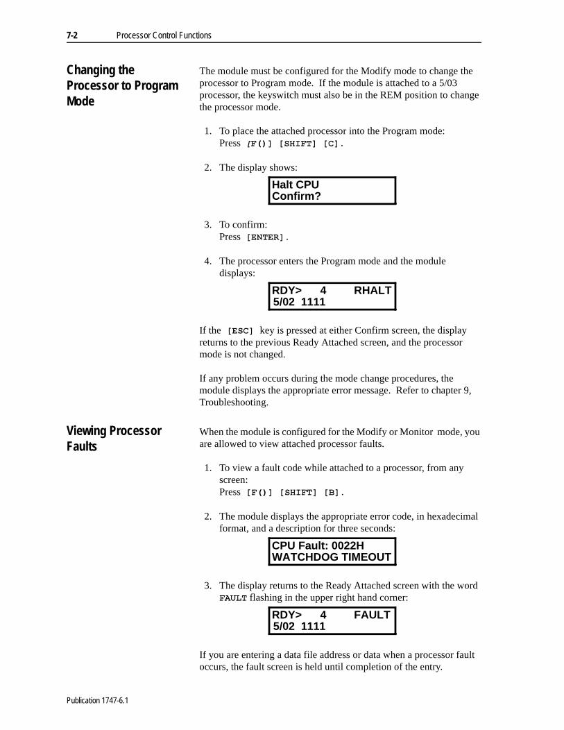
Changing the Processor to Program Mode
The module must be configured for the Modify mode to change the processor to Program mode. If the module is attached to a 5/03 processor, the keyswitch must also be in the REM position to change the processor mode.
1. To place the attached processor into the Program mode:Press [)��@�>6+,)7@�>&@�
2. The display shows:
3. To confirm:Press >(17(5@�
4. The processor enters the Program mode and the module displays:
If the�>(6&@�key is pressed at either Confirm screen, the display returns to the previous Ready Attached screen, and the processor mode is not changed.
If any problem occurs during the mode change procedures, the module displays the appropriate error message. Refer to chapter 9, Troubleshooting.
Viewing Processor Faults
When the module is configured for the Modify or Monitor mode, you are allowed to view attached processor faults.
1. To view a fault code while attached to a processor, from any screen:Press >)��@�>6+,)7@�>%@�
2. The module displays the appropriate error code, in hexadecimal format, and a description for three seconds:
3. The display returns to the Ready Attached screen with the word )$8/7 flashing in the upper right hand corner:
If you are entering a data file address or data when a processor fault occurs, the fault screen is held until completion of the entry.
Confirm?Halt CPU
RDY> 4 RHALT5/02 1111
WATCHDOG TIMEOUTCPU Fault: 0022H
RDY> 4 FAULT5/02 1111
Publication 1747-6.1

Processor Control Functions 7-3
Clearing Processor Faults
The module must be configured for the Modify mode to clear recoverable faults in the attached processor.
1. You may first choose to view a fault condition as described in the previous section.
2. To clear a fault, initiate the Clear Fault procedure from any screen:Press >)��@�>6+,)7@�>7@�
3. If the DTAM is not attached to a 5/03 with the keyswitch in RUN, the fault clears, and the processor is placed in the Program mode.
4. The Ready Attached screen displays:
5. You may now return the processor to the Run mode or initiate other module functions.
For additional information on faults and fault codes refer to chapter 9, Troubleshooting.
!ATTENTION: If the DTAM is attached to a 5/03 and the processor keyswitch is in the RUN position when you start to clear the fault, the processor enters the RUN mode once the fault is cleared.
RDY> 4 RHALT5/02 1111
Important: Before trying to place the processor in the Run mode, you must ensure that the cause of the fault has been corrected. If it is not rectified, the processor returns to the faulted condition as soon as you attempt to place it in Run mode.
Publication 1747-6.1

7-4 Processor Control Functions
Transferring Memory from EEPROM to RAM
You may transfer a program between processor EEPROM and RAM memory.
To transfer EEPROM to RAM, from any display:
1. Configure the module for the Modify mode.
2. Make sure the processor is in the Program mode.
3. To initiate the memory transfer:Press >)��@�>6+,)7@�>5@�
4. The module displays:
5. To confirm:Press >(17(5@�To abort the memory transfer:Press >(6&@�� The display returns to the previous ReadyAttached screen.
6. When the transfer is initiated, the module displays:
7. If the memory transfer is successful, the module displays:
If the program contained in the EEPROM is password-protected,you are required to re-enter the password at this point.
8. When the transfer is complete (or the password is entered, if required), the module displays the Ready Attached screen:
If an error occurs during the transfer, an error message displays on the bottom line of the display. Refer to chapter 9, Troubleshooting.
Confirm?PROM -> CPU RAM,
Working . . . .PROM -> CPU RAM,
Transfer SuccessPROM -> CPU RAM,
RDY> 4 RHALT5/02 1111
Publication 1747-6.1

Processor Control Functions 7-5
Transferring Memory from RAM to EEPROM
To transfer a program from processor RAM to EEPROM memory, from any display:
1. Configure the module for the Modify mode.
2. Make sure the processor is in the Program mode.
3. To initiate the memory transfer:Press >)��@�>6+,)7@�>1@�
4. The module displays:
5. To confirm:Press �>(17(5@�If the >(6&@ key is pressed at the Confirm screen, the displayreturns to the previous Ready Attached screen, and the memorytransfer is aborted.
6. When the transfer is initiated, the module displays:
7. If the memory transfer is successful, the module displays:
8. When the transfer is complete, the module returns to the Ready Attached screen.
If an error occurs during the transfer, an error message displays on the bottom line of the display. Refer to chapter 9, Troubleshooting.
Confirm?CPU RAM -> PROM,
Working . . . .CPU RAM -> PROM,
Transfer SuccessCPU RAM -> PROM,
Publication 1747-6.1

7-6 Processor Control Functions
Publication 1747-6.1
Chapter 8
Message Capability
This chapter provides:
• an overview of the message types
• programming parameters for the MSG instruction
• control block configuration for the 5/02 and 5/03 MSG instructions
• operational descriptions of the message types
• sample SLC 5/02 user programs
Message Overview The module supports six types of messages. The table below describes the functions of each:
Other module message capabilities are:
• display Write messages from any DH485 network device withmessage capability
• display messages in the Monitor or Modify modes
• enter data in the Monitor or Modify modes
• message overwrite protection
Message Type Functions
8-Word16 charactersDisplayed on one lineDisplay-only
16-Word32 charactersDisplayed on two linesDisplay-only
12-Word16 charactersOperator replyInitial value of zero
13-Word16 charactersOperator replyUser-defined initial value
18-Word
16 charactersOperator replyUser-defined initial valueUser-defined acknowledge bit addresses
1-Word Clear message
Important: SLC 500 Fixed and SLC 5/01 Modular Controllers donot support message capability.
Publication 1747-6.1

8-2 Message Capability
the
Programming the MSG Instruction
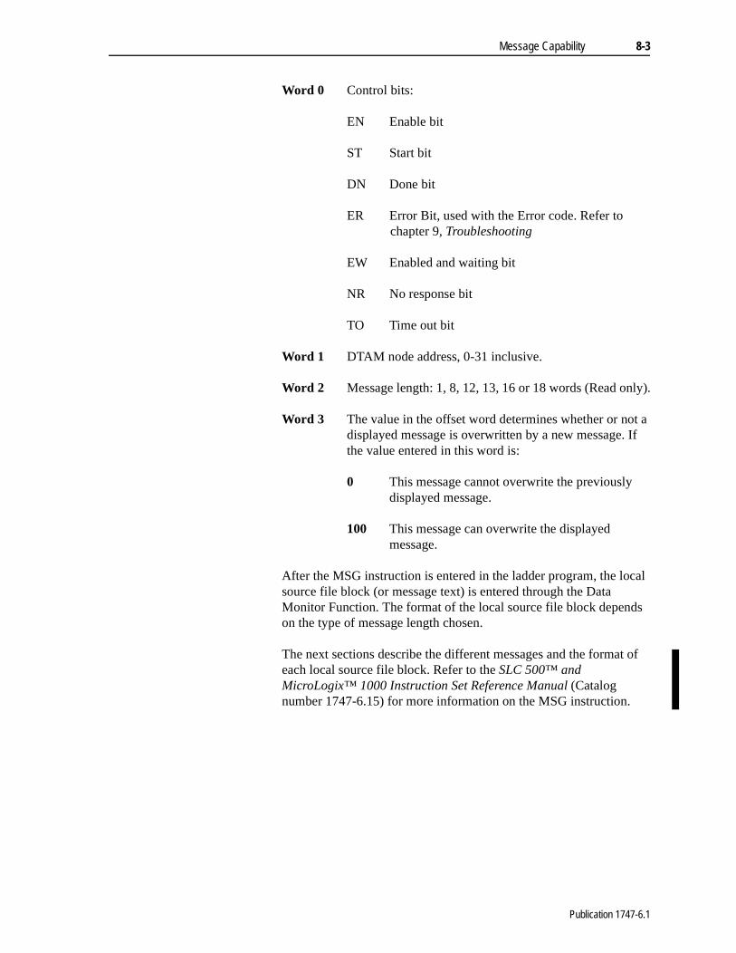
The DTAM message is configured in the 5/02 or 5/03 processor user program by selecting a message (MSG) instruction and entering the following parameters:
5/02 Control Block Configuration
Most of the MSG instruction parameters are stored in its associated control block. The “delivery” status and any error code of the message are also stored there. The information below describes message instruction control block layout necessary to display messages on the DTAM:
Message Type: Write
Target Device: 485CIF
Network Type (5/03 only): Local or Remote
Control Block Address:Starting address of an unused block of 7 words (5/02) or 14 words (5/03) in any bit or integer file(to store message status)
Source File Address:Starting address of an unused block or x words in any bit or integer file (to store message text), where x = message length or the DTAM message type
Target Node Address: DTAM node address (as defined in the module set-up procedure), 0 through 31 inclusive
Offset: Message overwrite capability: 0 for cannot overwrite or 100 for can overwrite
Message Length: Number of words in selected DTAM message type (1, 8, 12, 13, 16, or 18)
Channel (5/03 only):
Processor communication port:
1 for DH485 channel
or 0 for RS232 channel
Bit/Word
15 14 13 12 11 10 9 8 7 6 5 4 3 2 1 0
0 EN ST DN ER EW NR TO Error Code
1 DTAM Node Address
2 Message Length in Words (Read Only)
3 Offset Word (0 or 100)
4 Not Used
5 Not Used
6 Not Used
Publication 1747-6.1
Message Capability 8-3
Word 0 Control bits:
EN Enable bit
ST Start bit
DN Done bit
ER Error Bit, used with the Error code. Refer to chapter 9, Troubleshooting
EW Enabled and waiting bit
NR No response bit
TO Time out bit
Word 1 DTAM node address, 0-31 inclusive.
Word 2 Message length: 1, 8, 12, 13, 16 or 18 words (Read only).
Word 3 The value in the offset word determines whether or not a displayed message is overwritten by a new message. If the value entered in this word is:
0 This message cannot overwrite the previously displayed message.
100 This message can overwrite the displayed message.
After the MSG instruction is entered in the ladder program, the local source file block (or message text) is entered through the Data Monitor Function. The format of the local source file block depends on the type of message length chosen.
The next sections describe the different messages and the format of each local source file block. Refer to the SLC 500™ and MicroLogix™ 1000 Instruction Set Reference Manual (Catalog number 1747-6.15) for more information on the MSG instruction.
Publication 1747-6.1

8-4 Message Capability
the
5/03 Control Block Configuration
Most of the MSG instruction parameters are stored in its associated control block. The “delivery” status and any error code of the message are also stored there. The information below describes message instruction control block layout necessary to display messages on the DTAM:
Bit/Word
15 14 13 12 11 10 9 8 7 6 5 4 3 2 1 0
0 EN ST DN ER CO EW NR TO Error Code
1 DTAM Node Address
2 Message Length in Words (Read Only)
3 Offset Word (0 or 100)
4 Not Used
5 Not Used
6 Not Used
7 Reserved (Internal Messaging Bits)
8 Message Timer Preset
9 Message Timer Scaled Zero
10 Message Timer Accumulator
11 Reserved (Internal Use Only)
12 Reserved (Internal Use Only)
13 Reserved (Internal Use Only)
Publication 1747-6.1
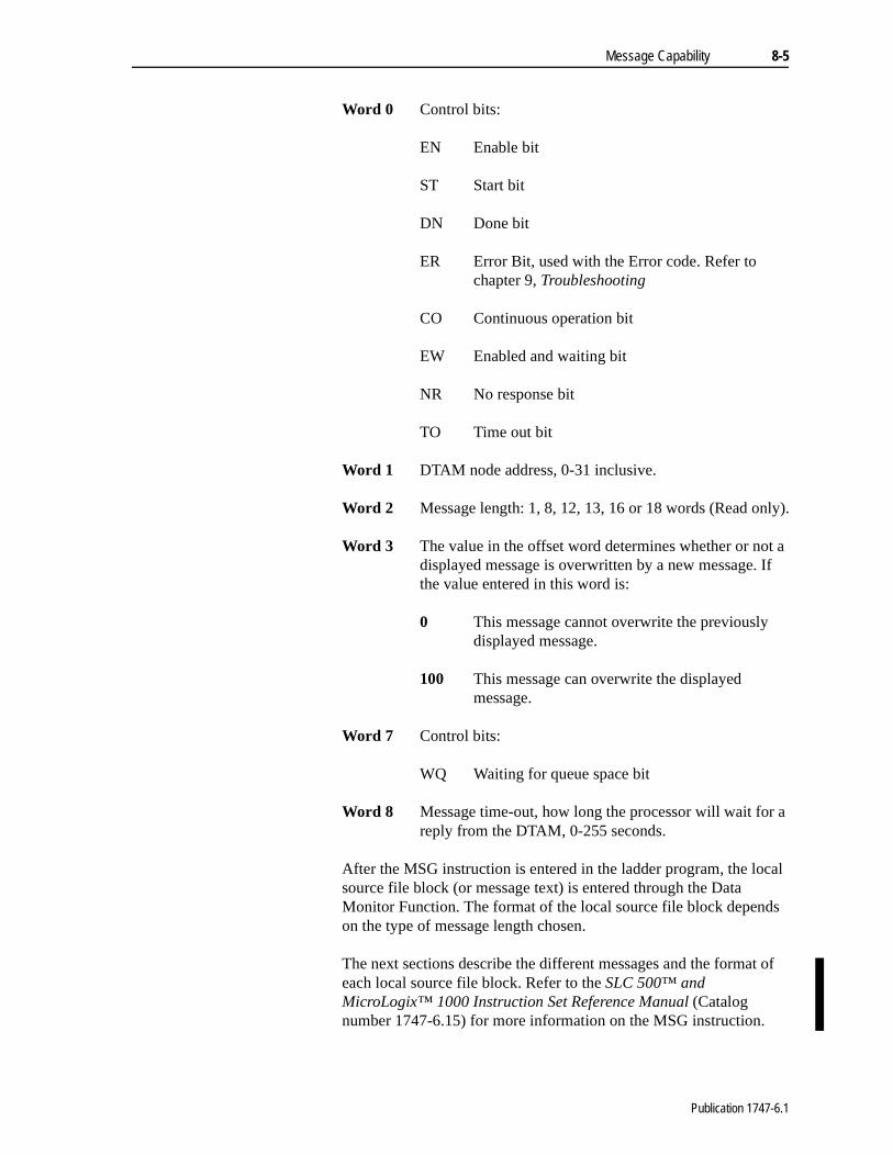
Message Capability 8-5
Word 0 Control bits:
EN Enable bit
ST Start bit
DN Done bit
ER Error Bit, used with the Error code. Refer to chapter 9, Troubleshooting
CO Continuous operation bit
EW Enabled and waiting bit
NR No response bit
TO Time out bit
Word 1 DTAM node address, 0-31 inclusive.
Word 2 Message length: 1, 8, 12, 13, 16 or 18 words (Read only).
Word 3 The value in the offset word determines whether or not a displayed message is overwritten by a new message. If the value entered in this word is:
0 This message cannot overwrite the previously displayed message.
100 This message can overwrite the displayed message.
Word 7 Control bits:
WQ Waiting for queue space bit
Word 8 Message time-out, how long the processor will wait for a reply from the DTAM, 0-255 seconds.
After the MSG instruction is entered in the ladder program, the local source file block (or message text) is entered through the Data Monitor Function. The format of the local source file block depends on the type of message length chosen.
The next sections describe the different messages and the format of each local source file block. Refer to the SLC 500™ and MicroLogix™ 1000 Instruction Set Reference Manual (Catalog number 1747-6.15) for more information on the MSG instruction.
Publication 1747-6.1
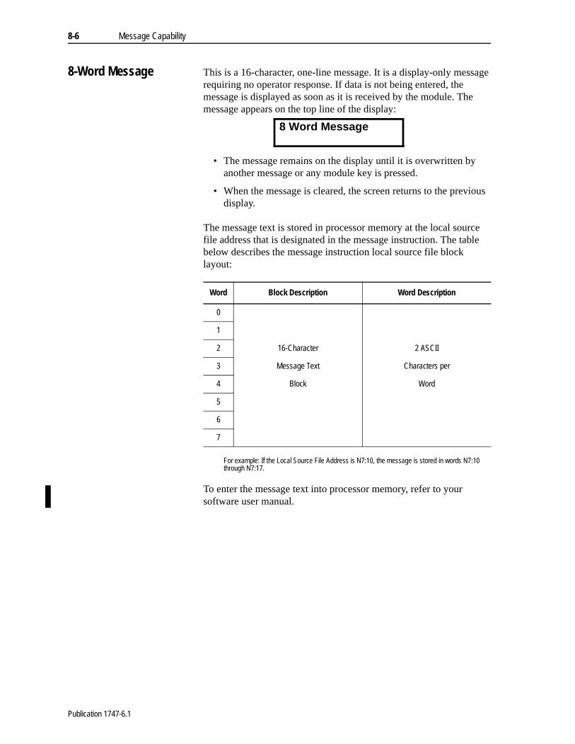
8-6 Message Capability
ious
ce le
8-Word Message This is a 16-character, one-line message. It is a display-only message requiring no operator response. If data is not being entered, the message is displayed as soon as it is received by the module. The message appears on the top line of the display:
• The message remains on the display until it is overwritten byanother message or any module key is pressed.
• When the message is cleared, the screen returns to the prevdisplay.
The message text is stored in processor memory at the local sourfile address that is designated in the message instruction. The tabbelow describes the message instruction local source file block layout:
For example: If the Local Source File Address is N7:10, the message is stored in words N7:10 through N7:17.
To enter the message text into processor memory, refer to your software user manual.
8 Word Message
Word Block Description Word Description
0
1
2 16-Character 2 ASCII
3 Message Text Characters per
4 Block Word
5
6
7
Publication 1747-6.1

Message Capability 8-7
ious
ce le
16-Word Message This is a 32-character, two-line message. It is a display-only message requiring no operator response. It is functionally identical to the 8-word message except in length. The message appears on both lines of the display:
• The message remains on the display until it is overwritten byanother message or any module key is pressed.
• When the message is cleared, the screen returns to the prevdisplay.
The message text is stored in processor memory at the local sourfile address that is designated in the message instruction. The tabbelow describes the message instruction local source file block layout:
For example: If the Local Source File Address is N7:10, the message is stored in words N7:10 through N7:25.
To enter the message text into processor memory, refer to your software user manual.
16 Word MessageShown in 2 Lines
Word Block Description Word Description
0
123
456 32-Character 2 ASCII
7 Message Text Characters per8 Block Word9
101112
131415
Publication 1747-6.1
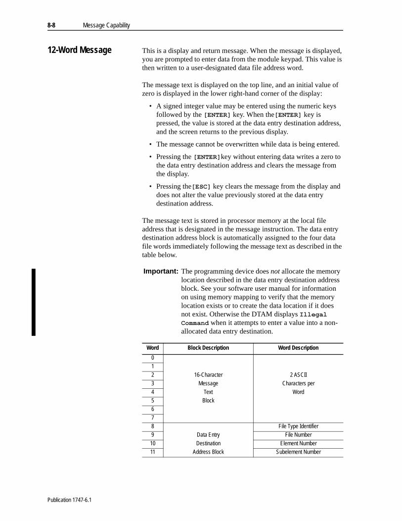
8-8 Message Capability
s
ress,
ed.
om
d
ntry ta the
ss
12-Word Message This is a display and return message. When the message is displayed, you are prompted to enter data from the module keypad. This value is then written to a user-designated data file address word.
The message text is displayed on the top line, and an initial value of zero is displayed in the lower right-hand corner of the display:
• A signed integer value may be entered using the numeric keyfollowed by the >(17(5@ key. When the>(17(5@ key is pressed, the value is stored at the data entry destination addand the screen returns to the previous display.
• The message cannot be overwritten while data is being enter
• Pressing the >(17(5@key without entering data writes a zero tothe data entry destination address and clears the message frthe display.
• Pressing the>(6&@ key clears the message from the display andoes not alter the value previously stored at the data entry destination address.
The message text is stored in processor memory at the local file address that is designated in the message instruction. The data edestination address block is automatically assigned to the four dafile words immediately following the message text as described in table below.
Important: The programming device does not allocate the memory location described in the data entry destination addreblock. See your software user manual for informationon using memory mapping to verify that the memory location exists or to create the data location if it does not exist. Otherwise the DTAM displays ,OOHJDO�&RPPDQG when it attempts to enter a value into a non-allocated data entry destination.
Word Block Description Word Description
0
12 16-Character 2 ASCII3 Message Characters per
4 Text Word5 Block6
78 File Type Identifier9 Data Entry File Number
10 Destination Element Number11 Address Block Subelement Number
Publication 1747-6.1

Message Capability 8-9
s
ress,
ed.
he
nd
e
ata
ss n
n-
13-Word Message This is a display and return message. When the message is displayed, you are required to enter data from the module keypad. It is functionally similar to the 12-word message except a user-defined initial value is displayed in the lower right-hand corner of the display:
• A signed integer value may be entered using the numeric keyfollowed by the >(17(5@ key. When the >(17(5@�key is pressed, the value is stored at the data entry destination addand the screen returns to the previous display.
• The message cannot be overwritten while data is being enter
• Pressing the >(17(5@�key without entering data writes the initial value to the data entry destination address and clears tmessage from the display.
• Pressing the�>(6&@ key clears the message from the display adoes not alter the value previously stored at the data entry destination address.
The message text is stored at the local file address, followed by thdata entry destination address block. The initial value word is automatically assigned to the next data file address following the dentry destination address block.
To enter the message text into processor memory, refer to your software user manual.
13 Word Message 123
Important: The programming device does not allocate the memory location described in the data entry destination addreblock. See your software user manual for informatioon using memory mapping to verify that the memory location exists or to create the data location if it does not exist. Otherwise the DTAM displays ,OOHJDO�&RPPDQG when it attempts to enter the value into a noallocated data entry destination.
Word Block Description Word Description
012 16-Character 2 ASCII
3 Message Characters per4 Text Word5 Block
678 File Type Identifier
9 Data Entry File Number10 Destination Element Number11 Address Block Subelement Number
12 Initial Value Word Signed Integer Value
Publication 1747-6.1

8-10 Message Capability
s
ress, reen
ed.
t for
tely
ss ur
et
18-Word Message This is a display and return message. When the message is displayed, you are required to enter data from the module keypad. It is functionally similar to the 13-word message except a user-defined acknowledge bit address block is included to indicate whether or not a message has been responded to.
The message display format is identical to the 13-word message:
• A signed integer value may be entered using the numeric keyfollowed by the�>(17(5@ key. When the >(17(5@ key is pressed, the value is stored at the data entry destination addthe user-defined message acknowledge bit is set, and the screturns to the previous display.
• The message cannot be overwritten while data is being enter
• Pressing the >(17(5@ key without entering data writes the initial value to the data entry destination address, sets the acknowledge bit, and clears the message from the display.
• Pressing the�>(6&@�key does not alter the value stored at thedata entry destination address, sets the user defined no acknowledge bit, and clears the message from the display.
The table on page 8-11 describes the local source file block layouthe 18-word message. The acknowledge bit address block is automatically assigned to the five data file address words immediafollowing the initial value word.
Important: The programming device does not allocate the memory location described in the data entry destination addreblock OR the acknowledge bit address block. See yosoftware user manual for information on using the memory mapping. Otherwise the DTAM displays ,OOHJDO�&RPPDQG when it attempts to enter the valueinto a non-allocated data entry destination or tries to sthe non-allocated acknowledge bit.
Publication 1747-6.1
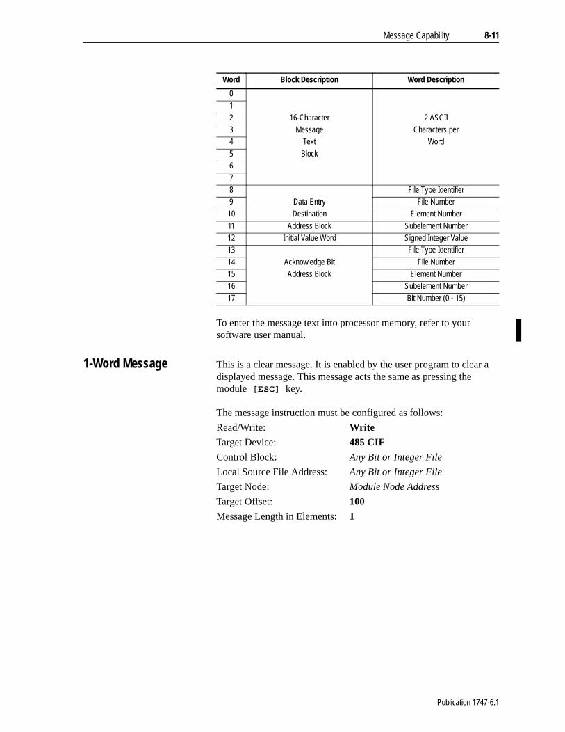
Message Capability 8-11
To enter the message text into processor memory, refer to your software user manual.
1-Word Message This is a clear message. It is enabled by the user program to clear a displayed message. This message acts the same as pressing the module�>(6&@�key.
The message instruction must be configured as follows:
Read/Write: Write
Target Device: 485 CIF
Control Block: Any Bit or Integer File
Local Source File Address: Any Bit or Integer File
Target Node: Module Node Address
Target Offset: 100
Message Length in Elements: 1
Word Block Description Word Description
01
2 16-Character 2 ASCII3 Message Characters per4 Text Word
5 Block67
8 File Type Identifier9 Data Entry File Number10 Destination Element Number
11 Address Block Subelement Number12 Initial Value Word Signed Integer Value13 File Type Identifier
14 Acknowledge Bit File Number15 Address Block Element Number16 Subelement Number
17 Bit Number (0 - 15)
Publication 1747-6.1

8-12 Message Capability
Application Example 1 Application example 1 uses two 18-word message instructions to enter variable data for high and low limits of a machine process. It also uses an 8-word message instruction to prompt you if data is not entered. The 5/02 ladder logic program is shown below. The data monitor displays for the message instructions and the user-defined data files are shown on the following page. The procedure to display the message is shown on page 8-16.
Example 1
0I:1.0
0
MSGREAD/WRITE MESSAGERead/WriteTarget DeviceControl BlockControl Block Length
WRITE485 CIF
N7:07
(EN)
(DN)
(ER)
117
(EN)
(DN)
(ER)
B3MSGREAD/WRITE MESSAGERead/WriteTarget DeviceControl BlockControl Block Length
WRITE485 CIF
N7:307
218
(EN)
(DN)
(ER)
B3MSGREAD/WRITE MESSAGERead/WriteTarget DeviceControl BlockControl Block Length
WRITE485 CIF
N7:607
3CLRCLEARDest B3:1
0000000000000000
B3
20
4 END
18-word Write Message instruction for low level data
18-word Write Message instructions for high level data
8-word Write Message instruction for no data entry
Reset Message acknowledge bits
Message trigger input
Acknowledge Bit from message in rung 0
No-acknowledge bits from messages in rungs 0 and 1
Operation NotesRung 0Input instruction I:1.0/0 initiates the first message instruction. This message prompts you to enter a value for the low range of the machine process. The initial value indicates that a minimum value of one should be entered. The Data Entry Destination Address is N10:1. The Acknowledge Bit Address is B3:1.0/1 or B3/17.
Rung 1This input instruction B3/17, is the user-designated acknowledge bit from the first message instruction. It is used to initiate the second message which prompts you to enter a value for the high range of the machine process. The initial value indicates a maximum of 250 should be entered. The Data Entry Destination Address is N10:2. The Acknowledge Bit Address is B3:1.0/3 or B3/19.
Rung 2Input instructions B3/18 and B3/20 are the user-designated no-acknowledge bits from the previous message instructions. If the module [ESC] key is pressed before entering either or both values, the message will prompt you that no value has been entered.
Rung 3This Clear instruction is enabled every scan to reset the user-defined acknowledge and no-acknowledge bits to zero.
Rung 4This is the end of the user program.
Publication 1747-6.1

Message Capability 8-13
The following example is the data monitor display for the 18-word message instruction in Rung 0:
Below is the data monitor display for the message control block and the local source file, followed by an explanation of the data file.
For ease of viewing, N7:10 through N7:17 are displayed in the ASCII radix. The rest of the file is displayed in Decimal.
7-word message control block: N7:0 through N7:6
N7:0 = 0 message status
N7:1 = 2 DTAM node address
N7:2 = 18 message length
N7:3 = 100 offset (overwrite capability)
N7:4 through N7:6 = unused
Read/Write:Target Device:Control Block:Local Source File Address:Target Node:Target Offset:Message Length in elements:
WRITE485 CIF
N7:0N7:10
210018
ignore if timed out:to be retried:
awaiting execution:
error:message done:
message transmitting:
TONREW
ERDNST
0000000
Address 0 1 2 3 4 5 6 7 8 9
N7:0 0 2 18 100 0 0 0 0 0 0
N7:10 E N T E R L O W R A N G E 7 10
N7:20 1 0 1 3 3 1 0 1 0 0
Publication 1747-6.1

8-14 Message Capability
18-word local source file: N7:10 through N7:27
N7:10 through N7:17 8-word message text
N7:18 through N7:21 data entry destination address
In this example the data entry destination address is N10:1. Memory locations N7:18 through N7:21 are assigned as follows:
N7:22 = 1 initial value word
N7:23 through N7:27 acknowledge bit address
In this example the acknowledge bit address is B3:1.0/1. Memory locations N7:23 through N7:27 are assigned as follows:
The following example is for the 18-word message in rung 1:
Below is the data monitor display for the message control block and the local source file, followed by an explanation of the data file.
For ease of viewing, N7:40 through N7:47 are displayed in the ASCII radix. The rest of the file is displayed in Decimal.
N10:1
File TypeFile Number
Element
N7:18=7N7:19=10
N7:20=1
Important: N10:1 must be allocated. See your software user manual. Otherwise the DTAM displays ,OOHJDO�&RPPDQG.
B3:1.0/1
File Type
File Number
Element
N7:23=3
N7:24=3N7:26=0
Subelement
Bit
N7:27=1
N7:25=1
Read/Write:Target Device:Control Block:Local Source File Address:Target Node:Target Offset:Message Length in elements:
WRITE485 CIF
N7:30N7:40
210018
ignore if timed out:to be retried:
awaiting execution:
error:message done:
message transmitting:
TONREW
ERDNST
0000000
Address 0 1 2 3 4 5 6 7 8 9
N7:30 0 2 18 100 0 0 0 0 0 0
N7:40 E N T E R H I G H R A N GE 7 10
N7:50 2 0 250 3 3 1 0 3 0 0
Publication 1747-6.1

Message Capability 8-15
7-word message control block: N7:30 through N7:36
N7:30 = 0 message status
N7:31 = 2 DTAM node address
N7:32 = 18 message length
N7:33 = 100 offset (overwrite capability)
N7:34 through N7:36 = unused
18-word local source file: N7:40 through N7:57
N7:40 through N7:47 8-word message text
N7:48 through N7:51 data entry destination address
In this example the data entry destination address is N10:2. Memory locations N7:48 through N7:51 are assigned as follows:
N7:52 = 250 initial value word
N7:53 through N7:57 acknowledge bit address
In this example the acknowledge bit address is B3:1.0/3. Memory locations N7:53 through N7:57 are assigned as follows:
The following example is for the 8-word message in rung 2:
N10:2
File TypeFile Number
Element
N7:48=7N7:49=10
N7:50=2
Important: N10:2 must be allocated. See your software user manual. Otherwise the DTAM displays ,OOHJDO�&RPPDQG.
B3:1.0/3
File Type
File Number
Element
N7:53=3
N7:54=3N7:56=0
Subelement
Bit
N7:57=3
N7:55=1
Read/Write:Target Device:Control Block:Local Source File Address:Target Node:Target Offset:Message Length in elements:
WRITE485 CIF
N7:60N7:70
2100
8
ignore if timed out:to be retried:
awaiting execution:
error:message done:
message transmitting:
TONREW
ERDNST
0000000
Publication 1747-6.1

8-16 Message Capability
the
Below is the data monitor display for the message control block and the local source file, followed by an explanation of the data file.
For ease of viewing, N7:60 through N7:67 are displayed in the ASCII radix. The rest of the file is displayed in Decimal.
7-word control block: N7:60 through N7:66
N7:60 = 0 message status
N7:61 = 2 DTAM node address
N7:62 = 8 message length
N7:63 = 100 offset (overwrite capability)
N7:64 through N7:66 = unused
8-word local source file: N7:70 through N7:77
N7:70 through N7:77 8-word message text
The ladder logic and data monitor examples on the previous pages must be programmed in SLC 5/02 processor memory for the following module message display:
1. When the input in rung 0 becomes true, the module displays this message and the suggested low value to be entered:
2. To enter a value:
• Accept the displayed value:Press >(17(5@�
• Use the numeric keys to change the value:Press >(17(5@�
3. The value is written to the data entry destination address, andmodule displays the next message in the sequence, with the suggested high value:
• Accept the displayed value:Press >(17(5@�
• Use the numeric keys to change the value:Press >(17(5@�
Address 0 1 2 3 4 5 6 7 8 9
N7:60 0 2 8 100 0 0 0 0 0 0
N7:70 N O V A L U E E N T E R E D 0 0
ENTER LOW RANGE1
ENTER HIGH RANGE250
Publication 1747-6.1

Message Capability 8-17
4. The value is written to the data entry destination address, and the module display returns to the screen displayed before the first message was received.If you press the >(6&@ key before the� >(17(5@� key whileeither of these messages is displayed, the value in the data entrydestination address remains unchanged, and the module dis-plays:
5. Press any key to clear this message. The display returns to the previous screen.
NO VALUE ENTERED
Publication 1747-6.1
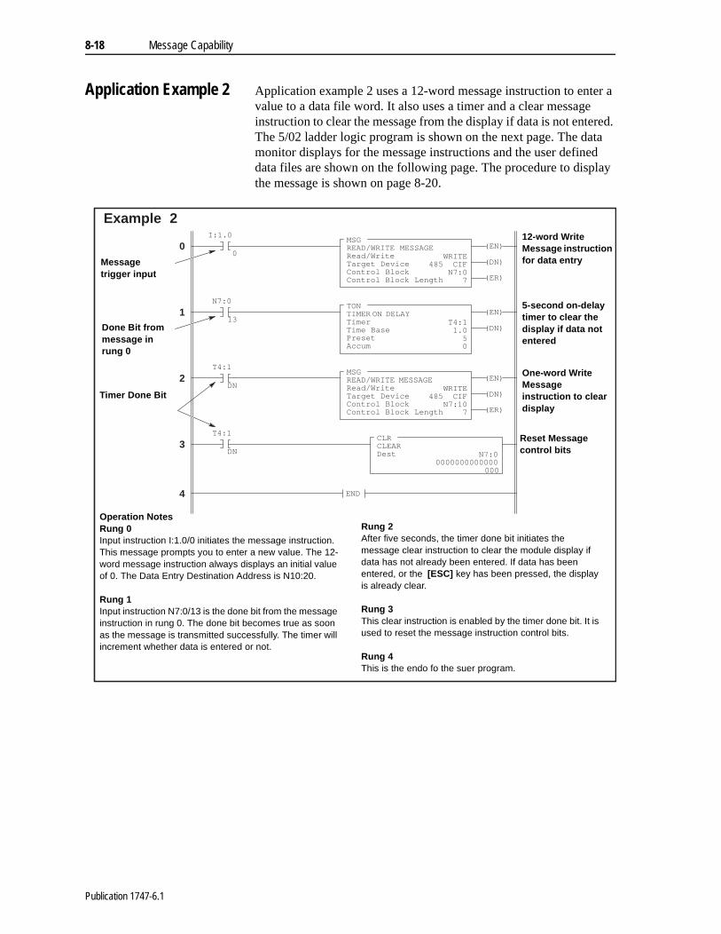
8-18 Message Capability
Application Example 2 Application example 2 uses a 12-word message instruction to enter a value to a data file word. It also uses a timer and a clear message instruction to clear the message from the display if data is not entered. The 5/02 ladder logic program is shown on the next page. The data monitor displays for the message instructions and the user defined data files are shown on the following page. The procedure to display the message is shown on page 8-20.
Example 2
0I:1.0
0
MSGREAD/WRITE MESSAGERead/WriteTarget DeviceControl BlockControl Block Length
WRITE485 CIF
N7:07
(EN)
(DN)
(ER)
113
(EN)
(DN)
N7:0TONTIMER ON DELAYTimerTime BasePresetAccum
T4:11.0
50
2DN
(EN)
(DN)
(ER)
T4:1MSGREAD/WRITE MESSAGERead/WriteTarget DeviceControl BlockControl Block Length
WRITE485 CIF
N7:107
3CLRCLEARDest N7:0
0000000000000000
4 END
DN
T4:1
12-word Write Message instruction for data entry
5-second on-delay timer to clear the display if data not entered
One-word Write Message instruction to clear display
Reset Message control bits
Message trigger input
Done Bit from message in rung 0
Timer Done Bit
Operation NotesRung 0Input instruction I:1.0/0 initiates the message instruction. This message prompts you to enter a new value. The 12-word message instruction always displays an initial value of 0. The Data Entry Destination Address is N10:20.
Rung 1Input instruction N7:0/13 is the done bit from the message instruction in rung 0. The done bit becomes true as soon as the message is transmitted successfully. The timer will increment whether data is entered or not.
Rung 2After five seconds, the timer done bit initiates the message clear instruction to clear the module display if data has not already been entered. If data has been entered, or the [ESC] key has been pressed, the display is already clear.
Rung 3This clear instruction is enabled by the timer done bit. It is used to reset the message instruction control bits.
Rung 4This is the endo fo the suer program.
Publication 1747-6.1
Message Capability 8-19
The following example is the data monitor display for the 12-word message instruction in Rung 0:
Below is the data monitor display for the message control block, followed by an explanation of the data file.
7-word message control block: N7:0 through N7:6
N7:0 = 0 message status
N7:1 = 2 DTAM node address
N7:2 = 12 message length
N7:3 = 100 offset (overwrite capability)
N7:4 through N7:6 = unused
Below is the data monitor display for the message local source file, followed by an explanation of the data file.
For ease of viewing, N10:0 through N10:7 are displayed in the ASCII radix. The rest of the file is displayed in Decimal.
12-word local source file: N10:0 through N10:11
N10:0 through N10:7 8-word message text
N10:8 through N10:11 data entry destination address
In this example the data entry destination address is N10:20. Memory locations N10:8 through N10:11 are assigned as follows:
Read/Write:Target Device:Control Block:Local Source File Address:Target Node:Target Offset:Message Length in elements:
WRITE485 CIF
N7:0N10:0
210012
ignore if timed out:to be retried:
awaiting execution:
error:message done:
message transmitting:
TONREW
ERDNST
0000000
Address 0 1 2 3 4 5 6 7 8 9
N7:0 0 2 12 100 0 0 0 0 0 0
Address 0 1 2 3 4 5 6 7 8 9
N10:0 E n t e r N e w V a l u e? 7 10
N10:10 20 0 0 0 0 0 0 0 0 0
N10:20
File TypeFile Number
Element
N10:8=7 N10:9=10N10:10=20
Publication 1747-6.1

8-20 Message Capability
The following example is for the 1-word message in rung 2:
Below is the data monitor display for the message control block and the local source file, followed by an explanation of the data file.
7-word control block: N7:10 through N7:16
N7:10 = 0 message status
N7:11 = 2 DTAM node address
N7:12 = 1 message length
N7:13 = 100 offset (overwrite capability)
N7:14 through N7:16 = unused
1-word local source file: N7:20
The ladder logic and data monitor examples on the previous pages must be programmed in SLC 5/02 processor memory for the following module message display:
1. When the input in rung 0 becomes true, the module displays this message:
2. To enter a value use the numeric keys. Then:Press >(17(5@�
3. The value writes to the data entry destination address, and the module display returns to the previous screen.If no value is entered, the value in the data entry destinationaddress remains unchanged, and the display returns to the previ-ous screen after five seconds.Pressing the�>(6&@ key while the message is displayed does notalter the value stored at the data entry address, and the displayreturns to the previous screen.
Read/Write:Target Device:Control Block:Local Source File Address:Target Node:Target Offset:Message Length in elements:
WRITE485 CIF
N7:10N7:20
2100
1
ignore if timed out:to be retried:
awaiting execution:
error:message done:
message transmitting:
TONREW
ERDNST
0000000
Address 0 1 2 3 4 5 6 7 8 9
N7:10 0 2 1 100 0 0 0 0 0 0
N7:20 0 0 0 0 0 0 0 0 0 0
ENTER NEW VALUE?0
Publication 1747-6.1

Chapter 9
Troubleshooting
This chapter describes the most common troubleshooting procedures. It describes:
• troubleshooting module problems using the CommunicationsLED
• troubleshooting module problems using the module display
• troubleshooting communications problems using the module display
• troubleshooting function problems using the module display
• troubleshooting MSG instruction error codes
• troubleshooting processor faults using the module display
Troubleshooting Module Problems Using the Communications LED
Refer to the following log to determine the status of the LED indicators:
Indicates the LED is OFF.
Indicates the LED is ILLUMINATED RED.
Indicates the LED is FLASHING RED.
Indicates the LED is ILLUMINATED GREEN.
Indicates the LED is FLASHING GREEN.
Publication 1747-6.1
9-2 Troubleshooting
TROUBLESHOOTING CONSIDERATIONS
COMMUNICATIONS INDICATOR DESCRIPTION PROBABLE CAUSES RECOMMENDED ACTION
OFF Module does not power up Bad cable connection
1. Verify proper connections on the module.
2. Verify proper connections to processor or link coupler.
3. Replace 1747-C10 Cable.
Power supply overloadedEvaluate chassis backplane loading for proper sizing of power supply.
No power to link coupler if on DH485 network
If no processor is connected to link coupler, provide 190mA or 24 VDC to screw terminals on link coupler.
Defective chassis power supply
1. Check for proper power supply connections.
2. Check for proper power suplly voltage.
3. Replace power supply.4. Disconnect module. Call
your Allen-Bradley service representative.
ILLUMINATED RED During power up Normal None.
During self diagnostics Normal None.
Hardware malfunction Defective power supply
1. Check for proper power supply voltage.
2. Replace power supply.3. Disconnect module. Call
your Allen-Bradley service representative.
Software malfunction Diagnostic failure 1. Consult error code on module display.
2. Reset module.3. Cycle power to module.
FLASHING RED Illegal network connection Improper module setup configuration Refer to module display.
ILLUMINATED GREEN Communicating on network Module configured for Monitor mode None.
FLASHING GREEN Communicating on network Module configured for Modify mode None.
Data being entered in Monitor Override mode None.
Publication 1747-6.1

Troubleshooting 9-3
Troubleshooting Module Problems Using the LCD
TROUBLESHOOTING CONSIDERATIONS
MODULE DISPLAY COMM LED PROBABLE CAUSES RECOMMENDED ACTION
ERROR 100 LED illuminated red ROM memory failed checksum test Reset module.
ERROR 200 LED illuminated red RAM failed Read/Write test Reset module.
ERROR 300 LED illuminated red Keypad malfunction Reset module.
ERROR 400 LED illuminated red Configuration memory failed checksum test
1. Cycle module power.2. Reconfigure module. Refer
to chapter 3, Module Setup Procedure.
Backlighting off LED illuminated red Insufficient power supply voltage Check power supply.
Backlighting flashes on and off LED illuminated red Insufficient or unregulated power supply voltage Check power supply.
LCD background is solid black Any Enclosure is too hot
1. Adjust display contrast, turn pot clockwise.
2. Operate within temperature specifications.
LCD characters are out of line AnyEnclosure is too hot or module is exposed to sudden temperature change.
Allow temperature to stabilize.
LCD is difficult to read Any Backlighting was Turned OffReconfigure module. Refer to chapter 3, Module Setup Procedure.
LCD characters unintelligible Any Water contamination in module Correct condition.
Improper initialization Reset module.
Module Cconfigured for a foreign language
Reconfigure module. Refer to chapter 3, Module Setup Procedure.
LCD appears faded or no display at all Any Enclosure too cold Adjust display contrast, turn
pot counter clockwise.
Module subjected to excessive heat or humidity
Disconnect module. Contact your local Allen-Bradley representative.
�
�
�
�
Publication 1747-6.1
9-4 Troubleshooting
Troubleshooting Communication Problems Using the LCD
TROUBLESHOOTING CONSIDERATIONS
GENERAL ERROR SCREEN ATTEMPTED FUNCTION PROBABLE CAUSES RECOMMENDED ACTION
Attach to node Illegal node address entered Node address must be within the range of 0 through 31.
Change processor to Run mode Module not attached to node Attach to proper node address.
Module not in Modify mode Change module to Modify mode.
Display fault Module not attached to node Attach to proper node address.Clear fault Module not attached to node Attach to proper node address.
Module not in modify node Change module to Modify mode.
Change processor to Program mode Module not attached to node Attach to proper node address.
Module not in Modify mode Change module to Modify mode.
EEPROM to RAM memory transfer Module not attached to node Attach to proper node address.
Module not in Modify mode Change module to Modify mode.
Processor in Run or Test mode Change processor to Program mode.
RAM to EEPROM memory transfer Module not attached to node Attach to proper node address.
Module not in Modify node Change module to Modify mode.
Processor in Run, Test or Fault mode
Change processor to Program mode or clear fault.
Processor contains no user program
Download a user program to processor from a programming device or HHT.
�
Publication 1747-6.1
Troubleshooting 9-5
TROUBLESHOOTING CONSIDERATIONS
GENERAL ERROR SCREEN ATTEMPTED FUNCTION PROBABLE CAUSES RECOMMENDED ACTION
Use a Quick Recall Function Quick recall function not defined
Assign an address to that function.
Quick recall function defined but that address is not defined in this processor
Attach to proper node address.
Enter Setup Procedure Module not in Modify mode Change module to Modify mode.
Enter Password Incorrect password entered Enter correct password.
Data Address Entry Incorrect format for address Reenter address correctly.Address not defined in this processor Allocate address in memory.
Data entry Module in the Monitor mode Change module to Modify mode.
Value out of range for file type Enter value within range.Address is read only (input or output file) Abort entry.
No response to a function key Address entry in progress Complete address entry or press the >(6&@key.
Data entry in progress Complete data entry or press the>(6&@key.
Illegal Command Responding to a message The Data file that the DTAM is trying to write to does not exist
See your software user manual for information on how to create the data entry destination or acknowledge bit locations.
Attach to a 5/03 processor
The firmware in the DTAM is less than revision 3.0 and does not support 5/03 communications
Verify the firmware revision number on the DTAM nameplate, and contact your local Allen-Bradley sales office for an upgrade.
Incompat Program Attach to a processorThe user program in the 5/03 processor is not supported by DTAM
Abort.
Contact your local Allen-Bradley sales office.
Illegal Network LED flashing red No other nodes are active on the network
Attach the required processor to the network.
One or more nodes on the network have an incorrect baud rate
Correct the baud rates.
Network is shorted or improperly wired
Check network cable connections.
Module has same node address as a 5/01 or fixed controller (point-to-point connection)
Reconfigure the module node address, refer to chapter 3, Module Setup Procedure.
The maximum node address of the previous node is lower than the module address
Change the maximum node address of the previous node.
Duplicate Node LED flashing redModule has same node address as a 5/02 or 5/03 (point-to-point connection)
Change the module node address.
LED flashing redModule has same node address as another node (DH485 network connection)
Change the module node address.
No Response LED illuminated green or flashing green
The node that the module is attached to has too many other nodes trying to communicate with it
Decrease the network traffic to the desired node address.
Publication 1747-6.1
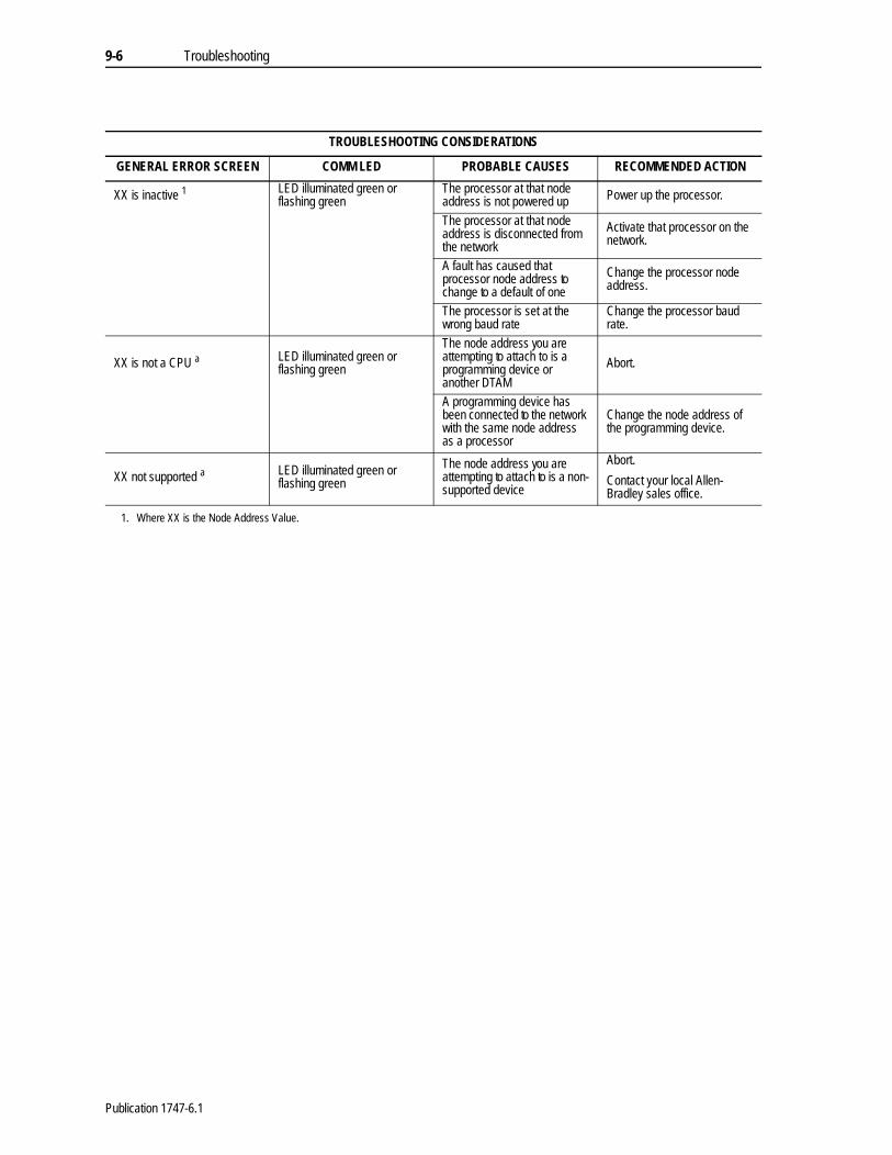
9-6 Troubleshooting
TROUBLESHOOTING CONSIDERATIONS
GENERAL ERROR SCREEN COMM LED PROBABLE CAUSES RECOMMENDED ACTION
XX is inactive 1 LED illuminated green or flashing green
The processor at that node address is not powered up Power up the processor.
The processor at that node address is disconnected from the network
Activate that processor on the network.
A fault has caused that processor node address to change to a default of one
Change the processor node address.
The processor is set at the wrong baud rate
Change the processor baud rate.
XX is not a CPU a LED illuminated green or flashing green
The node address you are attempting to attach to is a programming device or another DTAM
Abort.
A programming device has been connected to the network with the same node address as a processor
Change the node address of the programming device.
XX not supported a LED illuminated green or flashing green
The node address you are attempting to attach to is a non-supported device
Abort.
Contact your local Allen-Bradley sales office.
1. Where XX is the Node Address Value.
Publication 1747-6.1
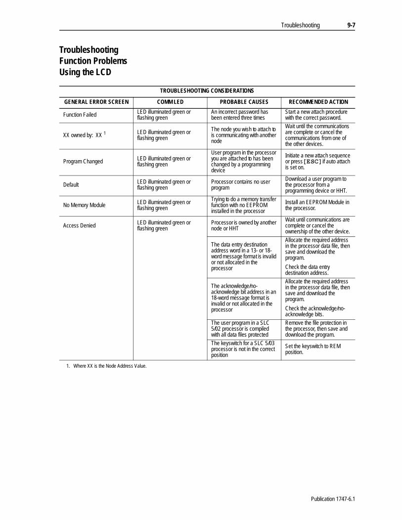
Troubleshooting 9-7
Troubleshooting Function Problems Using the LCD
TROUBLESHOOTING CONSIDERATIONS
GENERAL ERROR SCREEN COMM LED PROBABLE CAUSES RECOMMENDED ACTION
Function Failed LED illuminated green or flashing green
An incorrect password has been entered three times
Start a new attach procedure with the correct password.
XX owned by: XX 1 LED illuminated green or flashing green
The node you wish to attach to is communicating with another node
Wait until the communications are complete or cancel the communications from one of the other devices.
Program Changed LED illuminated green or flashing green
User program in the processor you are attached to has been changed by a programming device
Initiate a new attach sequence or press>(6&@if auto attach is set on.
Default LED illuminated green or flashing green
Processor contains no user program
Download a user program to the processor from a programming device or HHT.
No Memory Module LED illuminated green or flashing green
Trying to do a memory transfer function with no EEPROM installed in the processor
Install an EEPROM Module in the processor.
Access Denied LED illuminated green or flashing green
Processor is owned by another node or HHT
Wait until communications are complete or cancel the ownership of the other device.
The data entry destination address word in a 13- or 18-word message format is invalid or not allocated in the processor
Allocate the required address in the processor data file, then save and download the program.
Check the data entry destination address.
The acknowledge/no- acknowledge bit address in an 18-word message format is invalid or not allocated in the processor
Allocate the required address in the processor data file, then save and download the program.
Check the acknowledge/no-acknowledge bits.
The user program in a SLC 5/02 processor is compiled with all data files protected
Remove the file protection in the processor, then save and download the program.
The keyswitch for a SLC 5/03 processor is not in the correct position
Set the keyswitch to REM position.
1. Where XX is the Node Address Value.
Publication 1747-6.1

9-8 Troubleshooting
Troubleshooting MSG Instruction Error Codes
When an error condition occurs with a Message Instruction (MSG), the error code and its description are indicated in the Data Monitor display.
INSTRUCTION ERRORS
Error Code Fault Description
02H Target node is busy. The MSG instruction will automatically reload. If other messages are waiting, the message is placed at the bottom of the stack.
03H Target node cannot respond because message is too large.
04H Target node cannot respond because it does not understand the command parameters OR the control block may have been inadvertently modified.
05H Local processor is offline (possible duplicate node situation).
06H Target node cannot respond because requested function is not available.
07H Target node does not respond.
08H Target node cannot respond.
09H Local modem connection has been lost.
10H Target node cannot respond because of incorrect command parameters or unsupported command.
11H Local file has constant file protection.
12H Local channel configuration protocol error exists.
13H Local MSG configuration error in the Remote MSG parameters.
14H Local communication driver is incompatible with the MSG instruction.
15H Local channel configuration parameter error exists.
16H Target or Local Bridge address is higher than the maximum node address.
17H Local service is not supported.
18H Broadcast (Node Address 155) is not supported.
19HImproperly formatted Logical ASCII Address string. String not properly terminated with a NULL character or the string length does not match the value in the length parameter.
20H PCCC Description: Host has a problem and will not communicate.
30H PCCC Description: Remote station host is not there, disconnected, or shut down.
37H Message timed out in local processor.
38H Message disabled pending link response.
40H PCCC Description: Host could not complete function due to hardware fault.
50H Target node is out of memory.
60H Target node cannot respond because file is protected.
70H PCCC Description: Processor is in Program mode.
80H PCCC Description: Compatibility mode file missing or communication zone problem.
90H PCCC Description: Remote station cannot buffer command.
B0H PCCC Description: Remote station problem due to download.
C0H PCCC Description: Cannot execute command due to active IPBs.
D0H
No IP address configured for the network, -or-Bad command – unsolicited message error, -or-Bad address – unsolicited message error, -or-No privilege – unsolicited message error.
Publication 1747-6.1
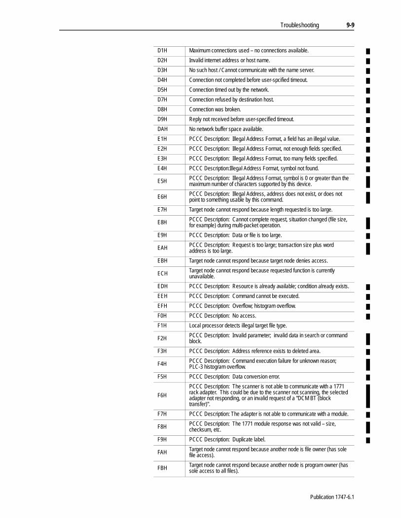
Troubleshooting 9-9
D1H Maximum connections used – no connections available.
D2H Invalid internet address or host name.
D3H No such host / Cannot communicate with the name server.
D4H Connection not completed before user-spcified timeout.
D5H Connection timed out by the network.
D7H Connection refused by destination host.
D8H Connection was broken.
D9H Reply not received before user-specified timeout.
DAH No network buffer space available.
E1H PCCC Description: Illegal Address Format, a field has an illegal value.
E2H PCCC Description: Illegal Address Format, not enough fields specified.
E3H PCCC Description: Illegal Address Format, too many fields specified.
E4H PCCC Description:Illegal Address Format, symbol not found.
E5H PCCC Description: Illegal Address Format, symbol is 0 or greater than the maximum number of characters supported by this device.
E6H PCCC Description: Illegal Address, address does not exist, or does not point to something usable by this command.
E7H Target node cannot respond because length requested is too large.
E8H PCCC Description: Cannot complete request, situation changed (file size, for example) during multi-packet operation.
E9H PCCC Description: Data or file is too large.
EAH PCCC Description: Request is too large; transaction size plus word address is too large.
EBH Target node cannot respond because target node denies access.
ECH Target node cannot respond because requested function is currently unavailable.
EDH PCCC Description: Resource is already available; condition already exists.
EEH PCCC Description: Command cannot be executed.
EFH PCCC Description: Overflow; histogram overflow.
F0H PCCC Description: No access.
F1H Local processor detects illegal target file type.
F2H PCCC Description: Invalid parameter; invalid data in search or command block.
F3H PCCC Description: Address reference exists to deleted area.
F4H PCCC Description: Command execution failure for unknown reason; PLC-3 histogram overflow.
F5H PCCC Description: Data conversion error.
F6H
PCCC Description: The scanner is not able to communicate with a 1771 rack adapter. This could be due to the scanner not scanning, the selected adapter not responding, or an invalid request of a "DCM BT (block transfer)".
F7H PCCC Description: The adapter is not able to communicate with a module.
F8H PCCC Description: The 1771 module response was not valid – size, checksum, etc.
F9H PCCC Description: Duplicate label.
FAH Target node cannot respond because another node is file owner (has sole file access).
FBH Target node cannot respond because another node is program owner (has sole access to all files).
Publication 1747-6.1
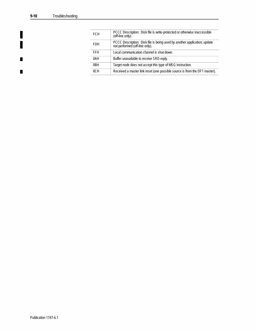
9-10 Troubleshooting
FCH PCCC Description: Disk file is write-protected or otherwise inaccessible (off-line only).
FDH PCCC Description: Disk file is being used by another application; update not performed (off-line only).
FFH Local communication channel is shut down.
0AH Buffer unavailable to receive SRD reply.
0BH Target node does not accept this type of MSG instruction.
0CH Received a master link reset (one possible source is from the DF1 master).
Publication 1747-6.1

Troubleshooting 9-11
Troubleshooting Processor Faults Using the LCD
If you are attached to a processor when a fault occurs, the module displays a fault code, in hexadecimal format, and a description of the fault. You may also attach to a faulted processor to view the source of a fault. The tables below describe the possible fault conditions in SLC 500 family processors.
The characters xx in the following codes represent the slot number, in hex. The characters xx become 1F if the exact slot can not be determined.
Slot Numbers in Hexadecimal
Slot XX Slot XX Slot XX
0 00 11 0B 22 161 01 12 0C 23 17
2 02 13 0D 24 183 03 14 0E 25 194 04 15 0F 26 1A
5 05 16 10 27 1B6 06 17 11 28 1C7 07 18 12 29 1D
8 08 19 13 30 1E9 09 20 1410 0A 21 15
PROCESSOR ERRORS
Error Code
Module Display Fault Description
0000 NO FAULT You have attempted to view a fault in a non-faulted processor.
0001 CORRUPT NVRAM NVRAM error.
0002 HARDWARE TIMEOUT Unexpected hardware watchdog timeout.
0003 AUTOLOAD FAILED Memory module memory error. This error can also occur when going to the REM Run mode.
0007 1
1. Error codes for 5/03 processor only
TRANSFER FAILED Failure during memory module transfer of autoload.
0008 1 CPU SOFTWARE ERR Internal software error.
0009 1 CPU HARDWARE ERR Internal hardware error.
0010 WRONG PROC. REV. The processor does not meet the proper revision level.
0011 FILE 2 MISSING The executable program file number 2 is absent.
0012 PROG MEM. ERROR The ladder program has a memory error.
0013 MEM MOD MISSINGThe required memory module is absent or either S:1/10 or S:1/11 is not set as required by the program.
0014 INT. FILE ERROR Internal file error.
0015 CFG. FILE ERROR Configuration file error.
Publication 1747-6.1
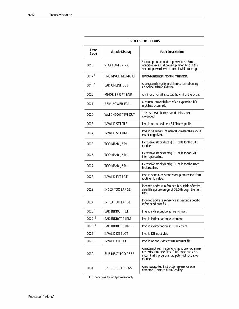
9-12 Troubleshooting
PROCESSOR ERRORS
Error Code Module Display Fault Description
0016 START AFTER P.F.Startup protection after power loss. Error condition exists at powerup when bit S:1/9 is set and powerdown occurred while running.
0017 1
1. Error codes for 5/03 processor only
PRC/MMOD MISMATCH NVRAM/memory module mismatch.
001F 1 BAD ONLINE EDIT A program integrity problem occurred during an online editing session.
0020 MINOR ERR AT END A minor error bit is set at the end of the scan.
0021 REM. POWER FAIL A remote power failure of an expansion I/O rack has occurred.
0022 WATCHDOG TIMEOUT The user watchdog scan time has been exceeded.
0023 INVALID STI FILE Invalid or non-existent STI interrupt file.
0024 INVALID STI TIME Invalid STI interrupt interval (greater than 2550 ms or negative).
0025 TOO MANY JSRs Excessive stack depth/JSR calls for the STI routine.
0026 TOO MANY JSRs Excessive stack depth/JSR calls for an I/O interrupt routine.
0027 TOO MANY JSRs Excessive stack depth/JSR calls for the user fault routine.
0028 INVALID FLT FILE Invalid or non–existent “startup protection” fault routine file value.
0029 INDEX TOO LARGEIndexed address reference is outside of entire data file space (range of B3:0 through the last file).
002A INDEX TOO LARGE Indexed address reference is beyond specific referenced data file.
002B 1 BAD INDRCT FILE Invalid indirect address file number.
002C 1 BAD INDRCT ELEM Invalid indirect address element.
002D 1 BAD INDRCT SUBEL Invalid indirect address subelement.
002E 1 INVALID DII SLOT Invalid DII input slot.
002F 1 INVALID DII FILE Invalid or non-existent DII interrupt file.
0030 SUB NEST TOO DEEP
An attempt was made to jump to one too many nested subroutine files. This code can also mean that a program has potential recursive routines.
0031 UNSUPPORTED INST An unsupported instruction reference was detected. Contact Allen-Bradley.
Publication 1747-6.1
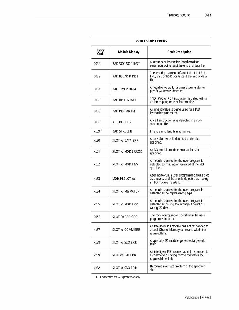
Troubleshooting 9-13
PROCESSOR ERRORS
Error Code Module Display Fault Description
0032 BAD SQC/SQO INST A sequencer instruction length/position parameter points past the end of a data file.
0033 BAD BSL/BSR INSTThe length parameter of an LFU, LFL, FFU, FFL, BSL or BSR points past the end of data file.
0034 BAD TIMER DATA A negative value for a timer accumulator or preset value was detected.
0035 BAD INST IN INTR TND, SVC or REF instruction is called within an interrupting or user fault routine.
0036 BAD PID PARAM An invalid value is being used for a PID instruction parameter.
0038 RET IN FILE 2 A RET instruction was detected in a non-subroutine file.
xx39 1
1. Error codes for 5/03 processor only
BAD STxx:LEN Invalid string length in string file.
xx50 SLOT xx DATA ERR A rack data error is detected at the slot specified.
xx51 SLOT xx MOD ERROR An I/O module runtime error at the slot specified.
xx52 SLOT xx MOD RMVA module required for the user program is detected as missing or removed at the slot specified.
xx53 MOD IN SLOT xxAt going-to-run, a user program declares a slot as unused, and that slot is detected as having an I/O module inserted.
xx54 SLOT xx MISMATCH A module required for the user program is detected as being the wrong type.
xx55 SLOT xx MOD ERRA module required for the user program is detected as having the wrong I/O count or wrong I/O driver.
0056 SLOT 00 BAD CFG The rack configuration specified in the user program is incorrect.
xx57 SLOT xx COMM ERRAn intelligent I/O module has not responded to a Lock Shared Memory command within the required limit.
xx58 SLOT xx SI/O ERR A specialty I/O module generated a generic fault.
xx59 SLOTxx SI/O ERRAn intelligent I/O module has not responded to a command as being completed within the required time limit.
xx5A SLOT xx SI/O ERR Hardware interrupt problem at the specified slot.
Publication 1747-6.1
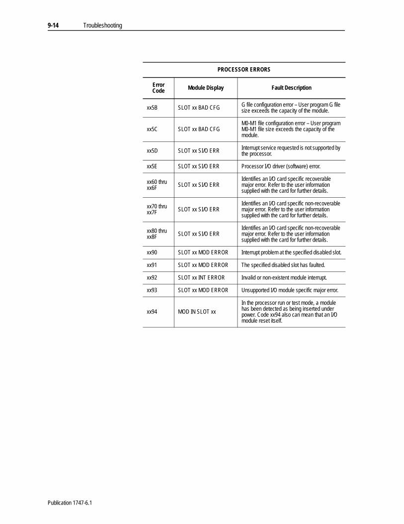
9-14 Troubleshooting
PROCESSOR ERRORS
Error Code Module Display Fault Description
xx5B SLOT xx BAD CFG G file configuration error – User program G file size exceeds the capacity of the module.
xx5C SLOT xx BAD CFGM0-M1 file configuration error – User program M0-M1 file size exceeds the capacity of the module.
xx5D SLOT xx SI/O ERR Interrupt service requested is not supported by the processor.
xx5E SLOT xx SI/O ERR Processor I/O driver (software) error.
xx60 thru xx6F SLOT xx SI/O ERR
Identifies an I/O card specific recoverable major error. Refer to the user information supplied with the card for further details.
xx70 thru xx7F SLOT xx SI/O ERR
Identifies an I/O card specific non-recoverable major error. Refer to the user information supplied with the card for further details.
xx80 thru xx8F SLOT xx SI/O ERR
Identifies an I/O card specific non-recoverable major error. Refer to the user information supplied with the card for further details.
xx90 SLOT xx MOD ERROR Interrupt problem at the specified disabled slot.
xx91 SLOT xx MOD ERROR The specified disabled slot has faulted.
xx92 SLOT xx INT ERROR Invalid or non-existent module interrupt.
xx93 SLOT xx MOD ERROR Unsupported I/O module specific major error.
xx94 MOD IN SLOT xx
In the processor run or test mode, a module has been detected as being inserted under power. Code xx94 also can mean that an I/O module reset itself.
Publication 1747-6.1
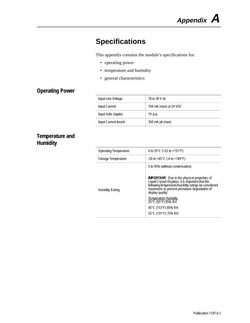
Appendix A
Specifications
This appendix contains the module’s specifications for:
• operating power
• temperature and humidity
• general characteristics
Operating Power
Temperature and Humidity
Input Line Voltage 18 to 30 V dc
Input Current 104 mA (max) at 24 VDC
Input Volts (ripple) 1V p-p
Input Current Inrush 350 mA pk (max)
Operating Temperature 0 to 55°C (+32 to +131°F)
Storage Temperature -20 to +65°C (-4 to +149°F)
Humidity Rating
5 to 95% (without condensation)
IMPORTANT: Due to the physical properties of Liquid Crystal Displays, it is important that the following temperature/humidity ratings be considered maximums to prevent premature degradation of display quality:
Temperature Humidity35°C (95°F) 95% RH
45°C (113°F) 85% RH
55°C (131°F) 75% RH
Publication 1747-6.1

A-2 Specifications
General Characteristics
Physical Dimensions
• Front Panel: 152.4 mm H x 139.7 mm W(6.0 in H x 5.5 in W)
• Back Case: 127.0 mm H x 101.6 mm W x 63.5 mm D (5.0 in H x 4.0 in W x 2.5 in D)
Mounting Torques .8 Nm (7.0 in-lb)
Operating Modes
The module can operate in one of two modes, Monitor or Modify. There is a three position terminal block provided for mode change. Access to the terminal is provided through the back case.
Display
The display is liquid crystal, using supertwist nematic fluid. The display format is 16 characters by 2 lines. A trim pot is provided for contrast adjustment. LCD backlighting is provided for viewing in low light conditions.
Keypad The keypad is of sealed membrane construction. The keys have an embossed rim and tactile feedback.
Status Indicator A bi-color LED is provided on the front of the module to provide communications and fault status.
Interconnect CableThe standard 1747-C10 cable is used as the interconnector between the module and a SLC 500 family processor or a DH-485 link coupler.
Vibration
0.38 mm (0.015 in) peak to peak displacement
2.5 g peak (max) acceleration
1 hr/axis
Noise Immunity Meets NEMA standard ICS 2-230
Certification
UL listed.
CSA certified.
Class I, Division 2, Groups A, B, C, D
Meets NEMA 12 and 13 enclosure applications
CE compliant for all applicable directives
Publication 1747-6.1
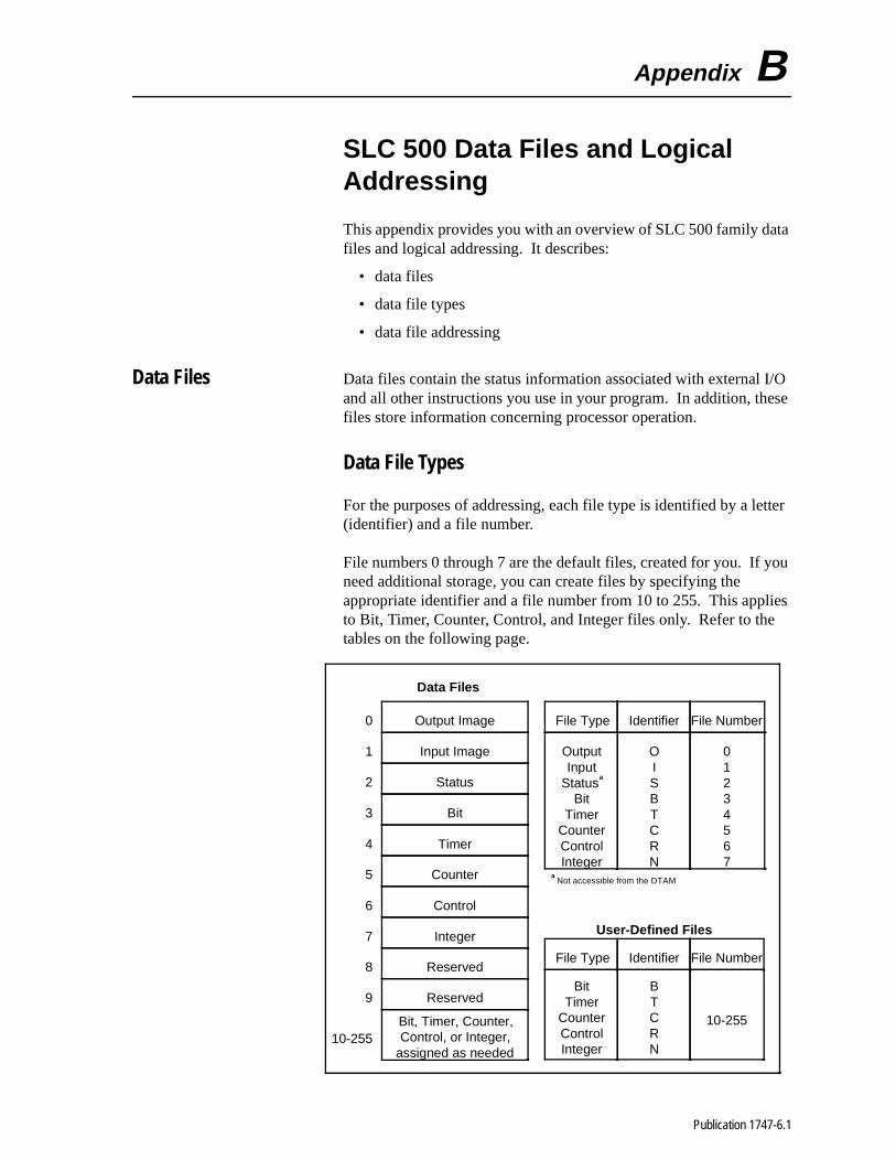
I/O ese
tter
ou
ies
Appendix B
SLC 500 Data Files and Logical Addressing
This appendix provides you with an overview of SLC 500 family data files and logical addressing. It describes:
• data files
• data file types
• data file addressing
Data Files Data files contain the status information associated with external and all other instructions you use in your program. In addition, thfiles store information concerning processor operation.
Data File Types
For the purposes of addressing, each file type is identified by a le(identifier) and a file number.
File numbers 0 through 7 are the default files, created for you. If yneed additional storage, you can create files by specifying the appropriate identifier and a file number from 10 to 255. This applto Bit, Timer, Counter, Control, and Integer files only. Refer to thetables on the following page.
Output Image File Type
OutputInput
StatusBit
TimerCounterControlInteger
Identifier
OISBTCRN
File Number
01234567
Input Image
Status
Bit
Timer
Counter
Control
Integer
Reserved
Reserved
0
1
2
3
4
5
6
7
8
9
10-255Bit, Timer, Counter,Control, or Integer,
assigned as needed
Data Files
User-Defined Files
File Type
BitTimer
CounterControlInteger
Identifier
BTCRN
File Number
10-255
Not accessible from the DTAM
a
a
Publication 1747-6.1
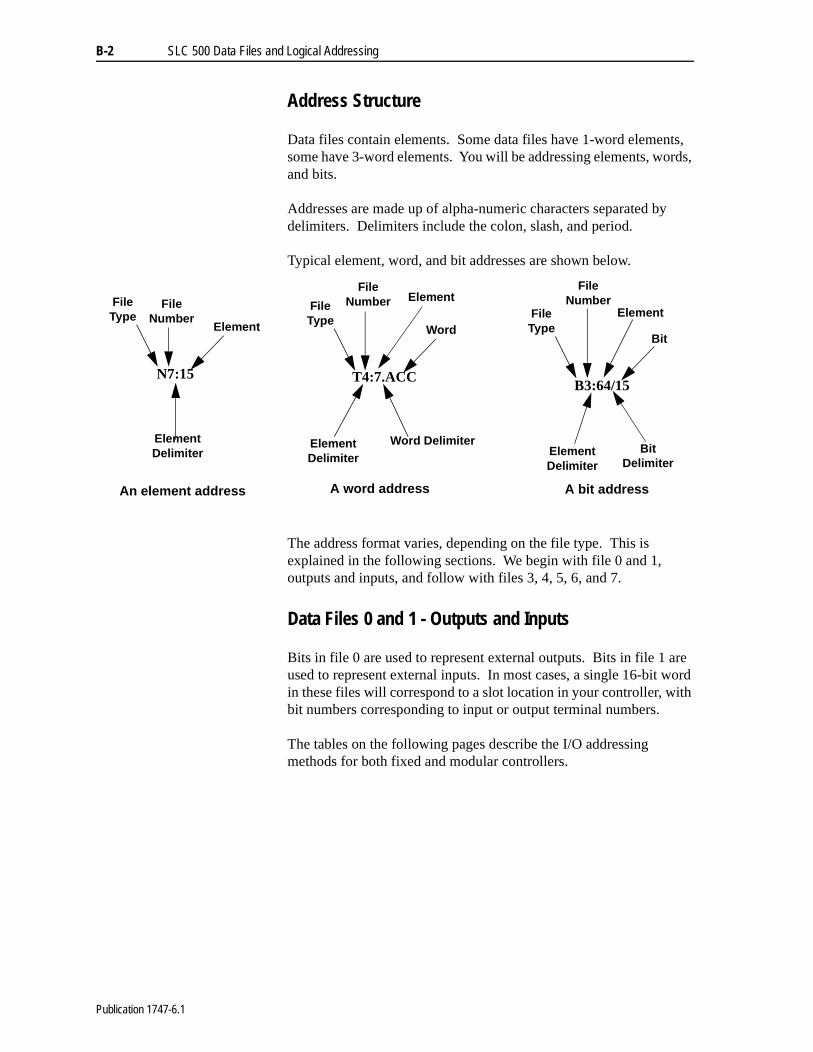
B-2 SLC 500 Data Files and Logical Addressing
Address Structure
Data files contain elements. Some data files have 1-word elements, some have 3-word elements. You will be addressing elements, words, and bits.
Addresses are made up of alpha-numeric characters separated by delimiters. Delimiters include the colon, slash, and period.
Typical element, word, and bit addresses are shown below.
The address format varies, depending on the file type. This is explained in the following sections. We begin with file 0 and 1, outputs and inputs, and follow with files 3, 4, 5, 6, and 7.
Data Files 0 and 1 - Outputs and Inputs
Bits in file 0 are used to represent external outputs. Bits in file 1 are used to represent external inputs. In most cases, a single 16-bit word in these files will correspond to a slot location in your controller, with bit numbers corresponding to input or output terminal numbers.
The tables on the following pages describe the I/O addressing methods for both fixed and modular controllers.
N7:15
Element
File Number
File Type
Element Delimiter
T4:7.ACC
Word
File NumberFile
Type
Element Delimiter
B3:64/15
Element
File Number
File Type
Element Delimiter
Element
Word DelimiterBit
Delimiter
Bit
An element address A word address A bit address
Publication 1747-6.1
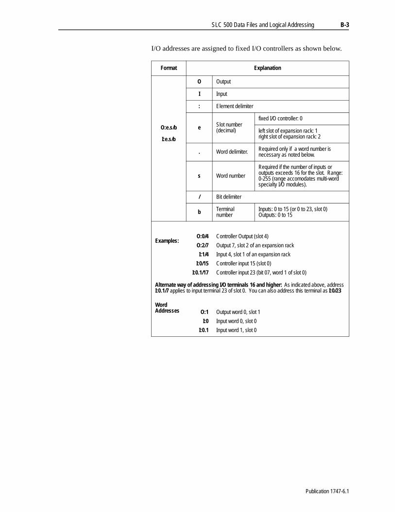
SLC 500 Data Files and Logical Addressing B-3
I/O addresses are assigned to fixed I/O controllers as shown below.
Format Explanation
O:e.s/b
I:e.s/b
O Output
I Input
: Element delimiter
e Slot number (decimal)
fixed I/O controller: 0
left slot of expansion rack: 1right slot of expansion rack: 2
. Word delimiter. Required only if a word number is necessary as noted below.
s Word number
Required if the number of inputs or outputs exceeds 16 for the slot. Range: 0-255 (range accomodates multi-word specialty I/O modules).
/ Bit delimiter
b Terminal number
Inputs: 0 to 15 (or 0 to 23, slot 0)Outputs: 0 to 15
Examples:O:0/4
O:2/7
I:1/4
I:0/15
I:0.1/17
Controller Output (slot 4)
Output 7, slot 2 of an expansion rack
Input 4, slot 1 of an expansion rack
Controller input 15 (slot 0)
Controller input 23 (bit 07, word 1 of slot 0)
Alternate way of addressing I/O terminals 16 and higher: As indicated above, address I:0.1/7 applies to input terminal 23 of slot 0. You can also address this terminal as I:0/23
Word Addresses O:1
I:0
I:0.1
Output word 0, slot 1
Input word 0, slot 0
Input word 1, slot 0
Publication 1747-6.1

B-4 SLC 500 Data Files and Logical Addressing
I/O addresses are assigned to modular controllers as shown in the table below:
Format Explanation
O:e.s/b
I:e.s/b
O Output
I Input
: Element delimiter
e Slot number (decimal)
Slot 0, adjacent to the power supply in the first rack, applies to the processor module (CPU). Succeeding slots are I/O slots, numbered from 1 to a maximum of 30.
. Word delimiter. Required only if a word number is necessary as noted below.
s Word number
Required if the number of inputs or outputs exceeds 16 for the slot. Range: 0-255 (range accomodates multi-word specialty I/O modules).
/ Bit delimiter
b Terminal number
Inputs: 0 to 15Outputs: 0 to 15
Examples:
O:3/15O:5/0
O:10/11I:7/8
I:2.1/3
Output 15, slot 3Output 0, slot 5Output 11, slot 10Input 8, slot 7Input 3, slot 2, word 1
Word Addresses O:5
O:5.1I:8
Output word 0, slot 5Input word 1, slot 5Input word 0, slot 8
Publication 1747-6.1

SLC 500 Data Files and Logical Addressing B-5
Data File 3 - Bit
File 3 is the bit file, used principally for relay logic instructions, shift registers, and sequencers. The maximum size of the file is 256 1-word elements, or a total of 4096 bits. You can address bits by specifying the element number (0-255) and the bit number within the element (0-15). You can also address bits simply by numbering them in sequence, from 0 to 4095.
You can also address elements of this file.
Format Explanation Examples
Bf:e/b
B Bit type file B3:3/14Bit 14, element 03
B3:252/0Bit 0, element 252
B3:9Bit 0-15, element 9
f File number.Number 3 is the default file. A file number between 10-255 can be used if additional storage is required.
: Element delimiter
e Element number
Ranges from 0 to 255. These are 1-word elements. 16-bits per element.
/ Bit delimiter.
b Bit number Bit location within the element. Ranges from 1 to 15.
Bf/b Bf/
Same as above.B3/62Bit 62
B3/4032Bit 4032b Bit number This is the numerical position of the bit
within the file. Ranges from 0 to 4095.
15 14 13 12 11 10 9 8 7 6 5 4
0
0
1
2
3
252
253
254
255
Element3 2 1Bit 14, element 3.Address B3:3/14
Can also be expressed as bit 62. Address B3/62
Bit 0, element 252.Address B3:252/0
Can also be expressed as bit 4032.Address B3/4032
Publication 1747-6.1

B-6 SLC 500 Data Files and Logical Addressing
Data File 4 - Timers
Timers are 3-word elements. Word 0 is the control word, word 1 stores the preset value, and word 2 stores the accumulator value. This is illustrated below.
Assign timer addresses as follows:
Format Explanation
Tf:e
T Timer
f File number.Number 4 is the default file. A file number between 10-255 can be used if additional storage is required.
: Element delimiter
e Element number
Ranges from 0 to 255. These are 3-word elements. See the figure above.
Examples: T4:0 Element 0, timer file 4.
Address bits and words by using the format TF:e.s/b where Tf:e is explained above, and
. is the word delimiters indicates subelement/ is the bit delimiterb indicates bit
T4:0/15T4:0/14T4:0/13
T4:0.1T4:0.2
T4:0.1/0T4:0.2/0
Enable bitTimer timing bitDone bit
Preset value of the timerAccumulated value of the timer
Bit 0 of the preset valueBit 0 of the accumulated value
EN14
TT DN
12 7 6 5
Internal Use15 13 11 10 9
Preset Value PRE
8
Accumulated Value ACC
4
0
0
1
2
Word3 2 1Timer Element
Addressable Bits Addressable Words
EN =EnableTT =Timer TimingDN =Done
PRE =Preset ValueACC =Accumulated Value
Bits labeled "Internal Use" are not addressable.
Publication 1747-6.1
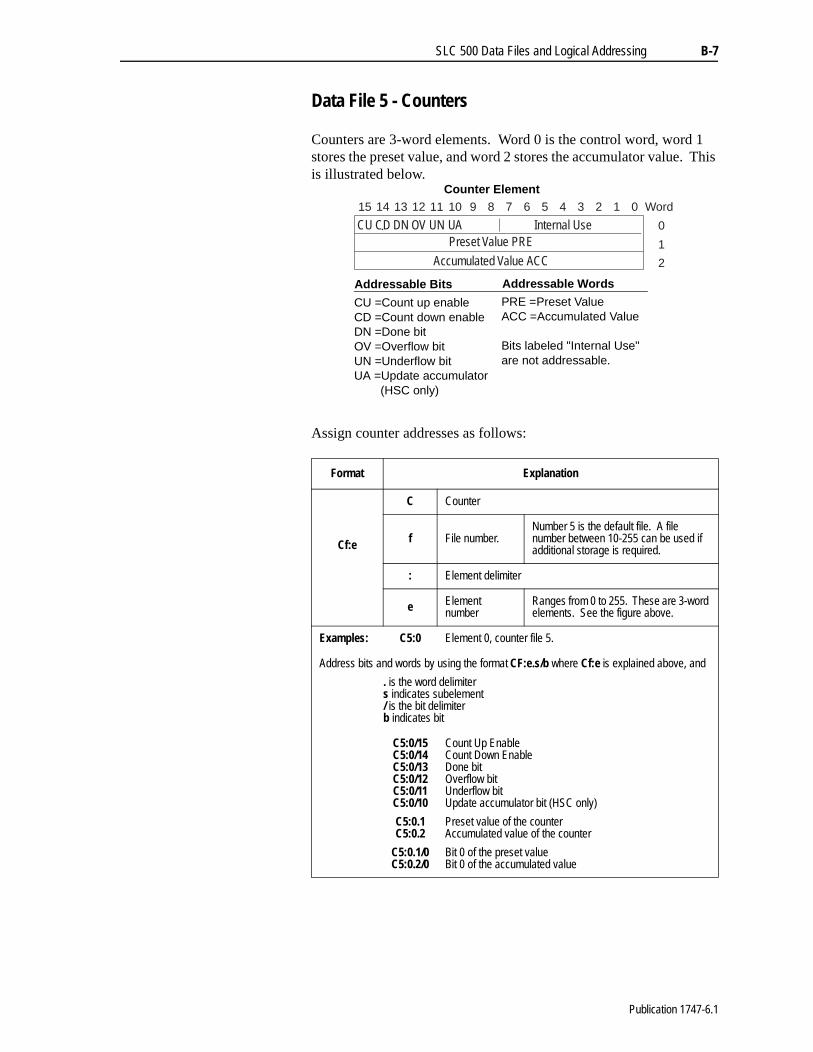
SLC 500 Data Files and Logical Addressing B-7
Data File 5 - Counters
Counters are 3-word elements. Word 0 is the control word, word 1 stores the preset value, and word 2 stores the accumulator value. This is illustrated below.
Assign counter addresses as follows:
Format Explanation
Cf:e
C Counter
f File number.Number 5 is the default file. A file number between 10-255 can be used if additional storage is required.
: Element delimiter
e Element number
Ranges from 0 to 255. These are 3-word elements. See the figure above.
Examples: C5:0 Element 0, counter file 5.
Address bits and words by using the format CF:e.s/b where Cf:e is explained above, and
. is the word delimiters indicates subelement/ is the bit delimiterb indicates bit
C5:0/15C5:0/14C5:0/13C5:0/12C5:0/11C5:0/10
C5:0.1C5:0.2
C5:0.1/0C5:0.2/0
Count Up EnableCount Down EnableDone bitOverflow bitUnderflow bitUpdate accumulator bit (HSC only)
Preset value of the counterAccumulated value of the counter
Bit 0 of the preset valueBit 0 of the accumulated value
CU CD14
DN12
OV UN UA7 6 5
Internal Use15 13 11 10 9
Preset Value PRE
8
Accumulated Value ACC
4
0
0
1
2
Word3 2 1
Counter Element
Addressable Bits Addressable Words
CU =Count up enableCD =Count down enableDN =Done bitOV =Overflow bitUN =Underflow bitUA =Update accumulator
(HSC only)
PRE =Preset ValueACC =Accumulated Value
Bits labeled "Internal Use" are not addressable.
Publication 1747-6.1
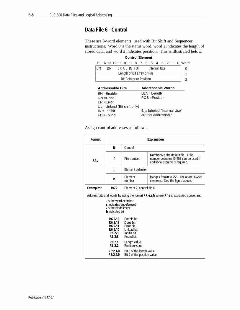
B-8 SLC 500 Data Files and Logical Addressing
Data File 6 - Control
These are 3-word elements, used with Bit Shift and Sequencer instructions. Word 0 is the status word, word 1 indicates the length of stored data, and word 2 indicates position. This is illustrated below.
Assign control addresses as follows:
Format Explanation
Rf:e
R Control
f File number.Number 6 is the default file. A file number between 10-255 can be used if additional storage is required.
: Element delimiter
e Element number
Ranges from 0 to 255. These are 3-word elements. See the figure above.
Examples: R6:2 Element 2, control file 6.
Address bits and words by using the format RF:e.s/b where Rf:e is explained above, and
. is the word delimiters indicates subelement/ is the bit delimiterb indicates bit
R6:2/15R6:2/13R6:2/11R6:2/10R6:2/9R6:2/8
R6:2.1R6:2.2
R6:2.1/0R6:2.2/0
Enable bitDone bitError bitUnload bitInhibit bitFound bit
Length valuePosition value
Bit 0 of the length valueBit 0 of the position value
EN14
DN12
ER UL IN FD7 6 5
Internal Use15 13 11 10 9
Length of Bit array or File
8
Bit Pointer or Position
4
0
0
1
2
Word3 2 1
Control Element
Addressable Bits Addressable Words
EN =EnableDN =DoneER =ErrorUL =Unload (Bit shift only)IN = InhibitFD =Found
LEN =LengthPOS =Position
Bits labeled "Internal Use" are not addressable.
Publication 1747-6.1
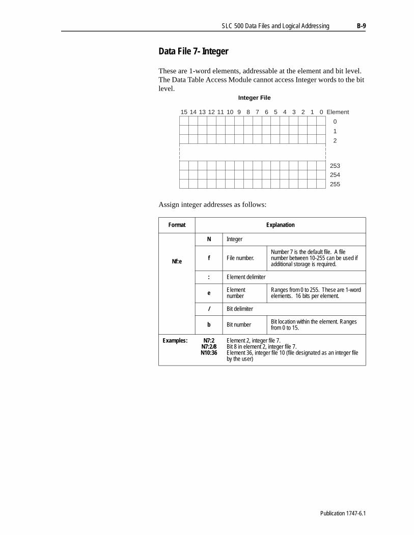
SLC 500 Data Files and Logical Addressing B-9
Data File 7- Integer
These are 1-word elements, addressable at the element and bit level. The Data Table Access Module cannot access Integer words to the bit level.
Assign integer addresses as follows:
Format Explanation
Nf:e
N Integer
f File number.Number 7 is the default file. A file number between 10-255 can be used if additional storage is required.
: Element delimiter
e Element number
Ranges from 0 to 255. These are 1-word elements. 16 bits per element.
/ Bit delimiter
b Bit number Bit location within the element. Ranges from 0 to 15.
Examples: N7:2N7:2/8N10:36
Element 2, integer file 7.Bit 8 in element 2, integer file 7.Element 36, integer file 10 (file designated as an integer file by the user)
15 14 13 12 11 10 9 8 7 6 5 4
0
0
1
2
253
254
255
Element3 2 1
Integer File
Publication 1747-6.1

B-10 SLC 500 Data Files and Logical Addressing
Publication 1747-6.1

Appendix C
Module Display Character Set
Display Character Table
This appendix provides a table to describe the module display characters and their binary equivalents. 00 through 1F Hex are reserved for system use.
Example: 41H = 01000001B = A
2x 3x 4x 5x 6x 7x Ax Bx Cx Dx Ex Fx
0010 0011 0100 0101 0110 0111 1010 1011 1100 1101 1110 1111
y0 0000
y1 0001
y2 0010
y3 0011
y4 0100
y5 0101
y6 0110
y7 0111
y8 1000
y9 1001
yA 1010
yB 1011
yC 1100
yD 1101
yE 1110
yF 1111
High Order4 bit
HexBinary
LowOrder 4 bit
Hex Binary
Publication 1747-6.1

C-2 Module Display Character Set
Publication 1747-6.1

Appendix D
Mounting Template
We have provided the following full-size template for your convenience in mounting the Data Table Access Module.
Using the Template Before you use this template, read the installation recommendations on page 2-1.
104.8 mm(4.125 in.)
95.76 mm(3.77 in.)
3.86 mm dia.(0.152 in.)4 holes
Scrape paint to ensure good ground.
114.3 mm(4.5 in.)
128.5 mm(5.06 in.)
Scrape paint to ensure good ground.
Publication 1747-6.1

D-2 Mounting Template
Publication 1747-6.1
Index I-1
Symbols.ACC . . . . . . . . . . . . . . . . . . . . . . . . . . . . . . . . . . 5-4
.LEN . . . . . . . . . . . . . . . . . . . . . . . . . . . . . . . . . . 5-4
.POS . . . . . . . . . . . . . . . . . . . . . . . . . . . . . . . . . . 5-4
.PRE . . . . . . . . . . . . . . . . . . . . . . . . . . . . . . . . . . 5-4
Numerics12-word message
application example . . . . . . . . . . . . . . . . 8-19
1747 AIC+. . . . . . . . . . . . . . . . . . . . . . . . . . . . . . 2-5
1747-AIC. . . . . . . . . . . . . . . . . . . . . . . . . . . . . . . 2-5
1747-C10 . . . . . . . . . . . . . . . . . . . . . . . . . . . . . . 2-5
1747-C-11 . . . . . . . . . . . . . . . . . . . . . . . . . . . . . . 2-5
18-word messageapplication example . . . . . . . . . . . . . . . . 8-13
1-word messageapplication example . . . . . . . . . . . . . . . . 8-20
8-word messageapplication example . . . . . . . . . . . . . . . . 8-15
Aaccess denied . . . . . . . . . . . . . . . . . . . . . . . . . . . 9-7
access holemaking adjustments through . . . . . . . . . . . 2-6
access portmaking adjustments through . . . . . . . . . . . 2-6
addressingchanging the node address. . . . . . . . . . . . 4-2data file address structure. . . . . . . . . . . . . B-2
adjustmentsmonitor mode . . . . . . . . . . . . . . . . . . . . . . 2-6
ASCII characters . . . . . . . . . . . . . . . . . . . . . . . . . C-1
BBackspace Function
during data file value entry . . . . . . . . . . . 5-14
bit addressesaddress format . . . . . . . . . . . . . . . . . . . . . B-5entering . . . . . . . . . . . . . . . . . . . . . . . . . . . 5-7
bit statuschanging at bit level . . . . . . . . . . . . . . . . 5-16changing at word level . . . . . . . . . . . . . . 5-15
Ccables
communication . . . . . . . . . . . . . . . . . . . . . 2-5interconnect. . . . . . . . . . . . . . . . . . . . . . . . 2-5
character display. . . . . . . . . . . . . . . . . . . . . . . . . C-1
clear messageapplication example . . . . . . . . . . . . . . . . 8-20
communications LEDstate changes . . . . . . . . . . . . . . . . . . . . . . 5-2
configuration and adjustmentsmonitor mode . . . . . . . . . . . . . . . . . . . . . . 2-6
connecting the equipment . . . . . . . . . . . . . . .2-4, 2-5to a DH-485 network . . . . . . . . . . . . . .2-4, 2-5to a SLC 500 family processor . . . . . . . . . 2-4
to an SLC 5/04 processor . . . . . . . . . . . . . 2-5
contrast, LCDadjust pot. . . . . . . . . . . . . . . . . . . . . . . . . . 2-6adjusting . . . . . . . . . . . . . . . . . . . . . . . . . . 9-3
control addressesaddress format . . . . . . . . . . . . . . . . . . . . . B-8entering . . . . . . . . . . . . . . . . . . . . . . . . . . . 5-8
counter addressesaddress format . . . . . . . . . . . . . . . . . . . . . B-7entering . . . . . . . . . . . . . . . . . . . . . . . . . . . 5-7
currentinput. . . . . . . . . . . . . . . . . . . . . . . . . . . . . . A-1input inrush . . . . . . . . . . . . . . . . . . . . . . . . A-1
cursor movementto the left . . . . . . . . . . . . . . . . . . . . . . . . . 5-15to the right . . . . . . . . . . . . . . . . . . . . . . . . 5-15
Cursor Right Functionduring binary data entry. . . . . . . . . . . . . . 5-15implementing . . . . . . . . . . . . . . . . . . . . . . 5-15
Multiple Cursor Right . . . . . . . . . . . 5-15Single Cursor Right . . . . . . . . . . . . 5-15
Ddata file values
changing bit status at bit level . . . . . . . . . 5-16changing bit status at word level . . . . . . . 5-15changing the sign of a value . . . . . . . . . . 5-14
data filesaddress structure. . . . . . . . . . . . . . . . . . . . B-2variations of . . . . . . . . . . . . . . . . . . . . . . . . 5-7
DEC key, explanation of . . . . . . . . . . . . . . . . . . . 3-2
deleting strings.ACC . . . . . . . . . . . . . . . . . . . . . . . . . . . . . 5-4.LEN . . . . . . . . . . . . . . . . . . . . . . . . . . . . . 5-4.POS . . . . . . . . . . . . . . . . . . . . . . . . . . . . . 5-4.PRE . . . . . . . . . . . . . . . . . . . . . . . . . . . . . 5-4
DH-485 network, connecting to. . . . . . . . . . 2-4, 2-5
dimensions, physical . . . . . . . . . . . . . . . . . . . . . . A-2
displaying data file addressesdifferent bit file addresses . . . . . . . . . . . . 5-12different control bits within elements . . . . 5-11different word addresses within elements 5-10
duplicate node error . . . . . . . . . . . . . . . . . . . . . . 9-5
Eequipment connection . . . . . . . . . . 2-4, 2-5
errorscorrecting. . . . . . . . . . . . . . . . . . . . . . . . . . 9-1function failed . . . . . . . . . . . . . . . . . . . . . . 9-7illegal command . . . . . . . . . . . . . . . . . . . . 9-5illegal network . . . . . . . . . . . . . . . . . . . . . . 9-5incompat program . . . . . . . . . . . . . . . . . . . 9-5no memory module . . . . . . . . . . . . . . . . . . 9-7no response. . . . . . . . . . . . . . . . . . . . . . . . 9-5program changed . . . . . . . . . . . . . . . . . . . 9-7
Ffunction failed error. . . . . . . . . . . . . . 9-7
Publication 1747-6.1

I-2 Index
Ggrounding the module . . . . . . . . . . . . .2-2
HHALT. . . . . . . . . . . . . . . . . . . . . . . . . . . . . . . . . . 4-3
Halt modeReady Attached screen display . . . . . . . . 4-3
humidity rating. . . . . . . . . . . . . . . . . . . . . . . . . . . A-1
Iillegal command error . . . . . . . . . . . . .9-5
illegal network error. . . . . . . . . . . . . . . . . . . . . . . 9-5
INC key, explanation of. . . . . . . . . . . . . . . . . . . . 3-2
incompat program error . . . . . . . . . . . . . . . . . . . 9-5
input and output addressesaddress format . . . . . . . . . . . . . . . . . . . . . B-2entering . . . . . . . . . . . . . . . . . . . . . . . . . . . 5-7
integer addressesaddresses format . . . . . . . . . . . . . . . . . . . B-9entering . . . . . . . . . . . . . . . . . . . . . . . . . . . 5-8
interconnect cable. . . . . . . . . . . . . . . . . . . . . . . . 2-5
Jjumper
alternative to . . . . . . . . . . . . . .2-7configuring the module with . . . . . . . . . . . 2-6
Kkeys, explanation of . . . . . . . . . . . . . . . . . . . . . . 3-1
keyswitchfor 5/03 operating modes . . . . . . . . . . . . . 4-3mounting user-supplied. . . . . . . . . . . . . . . 2-7
LLCD
contrast adjust pot. . . . . . . . . . . . . . . . . . . 2-6contrast adjustment. . . . . . . . . . . . . . . . . . 9-3
LEDstate changes . . . . . . . . . . . . . . . . . . . . . . 5-2
link coupler . . . . . . . . . . . . . . . . . . . . . . . . . . . . . 2-5
logical data file addressingcompared to quick access addressing . . . 5-6
Mmanuals, related . . . . . . . . . . . . . . . . . . . . . . . . . P-3
memory transfertroubleshooting using the LCD . . . . . . . . . 9-7
modify mode . . . . . . . . . . . . . . . . . . . . . . . . . . . . 2-6configuration and adjustments . . . . . . . . . 2-6functions performed . . . . . . . . . . . . . . . . . 5-2LED state . . . . . . . . . . . . . . . . . . . . . . . . . 5-2
module configuration and adjustmentsmonitor mode . . . . . . . . . . . . . . . . . . . . . . 2-6
monitor mode . . . . . . . . . . . . . . . . . . . . . . . . . . . 2-6configuration and adjustments . . . . . . . . . 2-6functions performed . . . . . . . . . . . . . . . . . 5-2LED state . . . . . . . . . . . . . . . . . . . . . . . . . 5-2
Monitor Overridefunctions performed . . . . . . . . . . . . . . . . . 5-2LED state . . . . . . . . . . . . . . . . . . . . . . . . . 5-2
moving the cursorto the left . . . . . . . . . . . . . . . . . . . . . . . . . 5-15to the right . . . . . . . . . . . . . . . . . . . . . . . . 5-15
NNEXT key, explanation of. . . . . . . . . . . 3-2
no memory module error. . . . . . . . . . . . . . . . . . . 9-7
no response error . . . . . . . . . . . . . . . . . . . . . . . . 9-5
node addresschanging . . . . . . . . . . . . . . . . . . . . . . . . . . 4-2
noise immunity . . . . . . . . . . . . . . . . . . . . . . . . . . A-2
Ooperating modes
displayed on Ready Attached screen . . 4-3monitor mode . . . . . . . . . . . . . . . . . . . . . . 5-1Monitor Override feature . . . . . . . . . . . . . . 5-1
operating powerinput current . . . . . . . . . . . . . . . . . . . . . . . A-1input current inrush . . . . . . . . . . . . . . . . . . A-1input line voltage . . . . . . . . . . . . . . . . . . . . A-1input volts (ripple) . . . . . . . . . . . . . . . . . . . A-1
output and input addressesaddress format . . . . . . . . . . . . . . . . . . . . . B-2entering . . . . . . . . . . . . . . . . . . . . . . . . . . . 5-7
PPREV key, explanation of. . . . . . . . . . . 3-2
PROG . . . . . . . . . . . . . . . . . . . . . . . . . . . . . . . . . 4-3
program changed error . . . . . . . . . . . . . . . . . . . . 9-7
Program modeReady Attached screen display. . . . . . . . . 4-3
publications, related . . . . . . . . . . . . . . . . . . . . . . P-3
Qquestions or comments on manual . . . . . . . . . . . P-4
quick access addressingcompared to logical addressing . . . . . . . . 5-6
Publication 1747-6.1

Index I-3
Rready screens . . . . . . . . . . . . . . . . . . . . . . . . . . . 3-7
Ready Attached screenduring Manual Attach procedure . . . 4-2text, operating mode . . . . . . . . . . . . 4-3
Ready Unattached screen. . . . . . . . . .3-3, 4-1during Manual Attach procedure . . . 4-1
REM position. . . . . . . . . . . . . . . . . . . . . . . . . . . . 4-3
RHALT . . . . . . . . . . . . . . . . . . . . . . . . . . . . . . . . 4-3
RRUN . . . . . . . . . . . . . . . . . . . . . . . . . . . . . . . . . 4-3
RTEST . . . . . . . . . . . . . . . . . . . . . . . . . . . . . . . . 4-3
RUN . . . . . . . . . . . . . . . . . . . . . . . . . . . . . . . . . . 4-3
Run modeReady Attached screen display . . . . .4-3
Ssetup mode
changing the setup configuration . . . . . . . 3-3
strain relief tab . . . . . . . . . . . . . . . . . . . . . . . . . . 2-2
Ttechnical product assistance. . . . . . . . . . . . . . . . P-4
temperatureoperating . . . . . . . . . . . . . . . . . . . . . . . . . . A-1storage . . . . . . . . . . . . . . . . . . . . . . . . . . . A-1
TEST. . . . . . . . . . . . . . . . . . . . . . . . . . . . . . . . . . 4-3
timer addressesaddress format . . . . . . . . . . . . . . . . . . . . . B-6entering . . . . . . . . . . . . . . . . . . . . . . . . . . . 5-7
torque . . . . . . . . . . . . . . . . . . . . . . . . . . . . . 2-2, A-2
Uuser-supplied keyswitch
connecting . . . . . . . . . . . . . . .2-7
Vvolts
input (ripple) . . . . . . . . . . . . . .A-1input line . . . . . . . . . . . . . . . . . . . . . . . . . . A-1
Publication 1747-6.1

I-4 Index
Publication 1747-6.1

Publication 1747-6.1

Publication 174Supercedes Publica
7-6.1 — August 1998 40072-041-01(B)tion Number 1747-6.1— November 1996 Copyright 1998 — Rockwell International Corporation. Printed in USA