1983-07_hp journal papers
DESCRIPTION
1983-07_HP Journal PapersTRANSCRIPT
M E W L E T T - P A C K A R D J O U R N A L
lowiitt ttii MM mi © Copr. 1949-1998 Hewlett-Packard Co.
H E W L E T T - P A C K A R D J O U R N A L Technical Informat ion f rom the Laborator ies of Hewlet t -Packard Company
JULY 1983 Volume 34 • Number 7
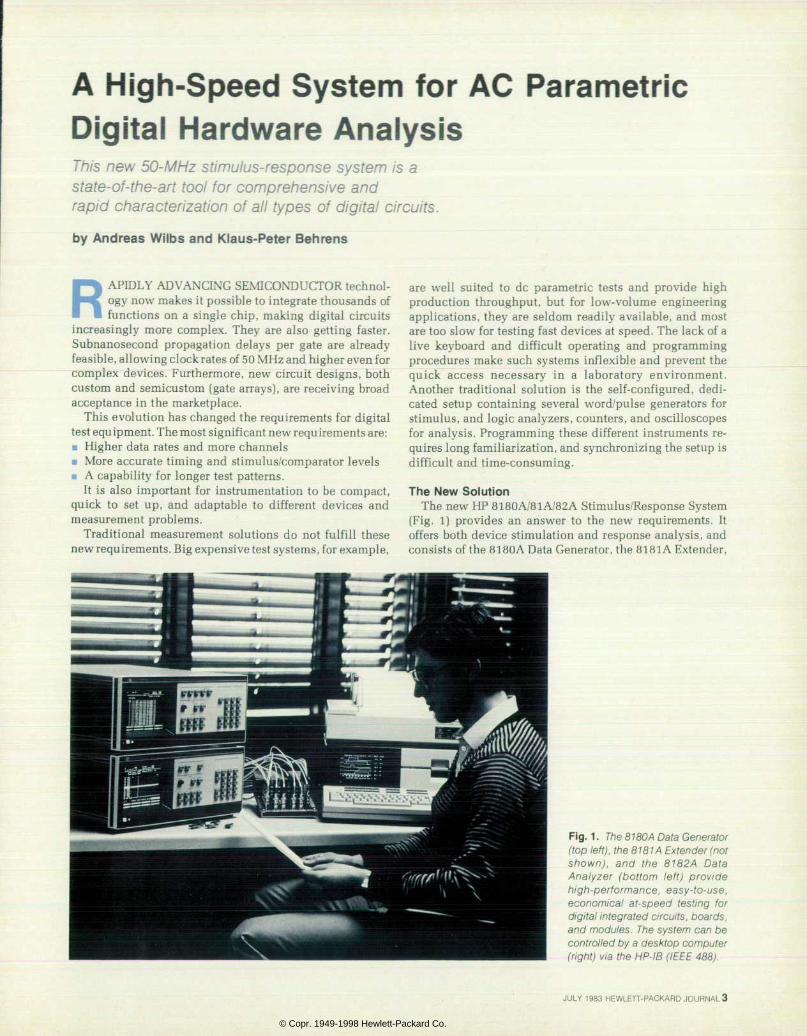
Contents: A H i g h - S p e e d S y s t e m f o r A C P a r a m e t r i c D i g i t a l H a r d w a r e A n a l y s i s , b y A n d r e a s W i l b s and Klaus-Peter Behrens Here 's a 50-MHz mul t ichannel s t imulus/ response system for test
ing d ig i ta l c i rcui ts at real is t ic speeds. A High-Speed Data Generator for Dig i ta l Test ing, by Ulr ich Hübner, Werner Berkel , Heinz Nüss le , and Jose f Becker I t o f fe rs h igh t im ing accuracy , p rec ise pu lse- leve l de f in i t ion ,
ease of operat ion, and versat i l i ty . H i g h - S p e e d D a t a A n a l y z e r T e s t s T h r e s h o l d a n d T i m i n g P a r a m e t e r s , b y D i e t e r K i b l e , B e r n h a r d R o t h , M a r t i n D i e t z e , a n d U l r i c h S c h o t t m e r T w o i n n o v a t i v e f e a t u r e s a r e p r o
grammable sampl ing po in t de lay and rea l - t ime compare mode. Data Eckhard Sof tware /F i rmware Des ign , by Rober to Mot to la and Eckhard Pau l A sk i l l ed t a s k t h e m a k e s f u l l u s e o f t h e i n t e r r u p t s t r u c t u r e o f t h e C P U . P o w e r S u p p l i e s f o r t h e S t i m u l u s / R e s p o n s e S y s t e m , b y U l r i c h O t t o a n d H o r s t L i n k T h e object ives were h igh load current and serv iceabi l i ty wi th in a rest r ic ted space. New Mul t i -F requency LCZ Meters Of fer H igher -Speed Impedance Measurements , by Tomio Wakasugi , Takeshi Kyo, and Toshio Tamamura These new inst ruments can be eas i ly
combined wi th a component handler for more rap id product ion- l ine tes t ing. Authors
In this Issue: Qual i ty is h igh on everyone's pr ior i ty l is t these days, and one of the pr inc ipa l paths to
[ qua l i t y i s tes t ing , thorough and rea l i s t i c , a t a l l phases o f the process o f des ign ing and producing a product. This month's issue deals with two famil ies of test instruments that are aimed resistors, assuring the quality of the myriad diodes, transistors, resistors, capacitors, induc tors, integrated circuits, circuit boards, and modules that go into electronic equipment. Each family capabilities a target range of testing applications and a repertoire of special capabilities needed in those appl icat ions.
On th i s t im ing cover a re th ree v iews , a t p rog ress ive ly f i ne r reso lu t ion , o f the t im ing diagram along a RAM (an integrated circuit random-access memory chip). Memory circuits l ike this one, along wi th microprocessors, gate arrays, and other d ig i ta l in tegrated c i rcu i ts ( ICs) are becoming faster and more complex at a start l ing rate — sometimes the next generation is announced before its predecessor is in produc t i on . The o f tha t p roduced th i s t im ing d iag ram i s des igned to keep up w i th the rap id l y chang ing s ta te o f the art detail. instruments, test fast, complex digital ICs at realistic speeds and in minute detail. This family of instruments, consist ing of the 8180A Data Generator, the 81 81 A Extender, and the 8182A Data Analyzer, is dist inguished by a t ime resolut ion of 100 picoseconds ( there are a mi l l ion picoseconds in a mi l l ionth of a second) and the analyzer 's programmable sampl ing point delay. These features make i t possib le to zero in on the br iefest of 1C events. You can read al l about the design of th is system on pages 3 to 31 .
While the high-performance 80A/81 A/82A System is designed for relatively low-volume testing of complex, high-performance digital inspection in engineering, quality assurance, depot maintenance, and certain kinds of incoming inspection and production testing, the 4276A and 4277 A LCZ Meters are aimed mainly at high-volume incoming inspection and product ion tes t ing o f d iscre te components (LCZ s tands for inductance-capac i tance- impedance) . They also have components uses in the engineering laboratory and in semiconductor evaluation. By testing components faster instruments and realistically than previously available equipment, these instruments improve the quality and lower handler several of the products we purchase. Fed by an automatic component handler (available from several manufacturers) , they ' l l check up to ten components per second and sor t them into as many as ten c lasses, and keep i t up hour af ter hour wi thout at tent ion. For repor t ing test data, they ' re compat ib le wi th computers and plotters, and for real ist ic test ing, they offer a var iety of test f requencies and vol tages. The designers tel l the i r s tory on pages 32 to 38.
-R.P. Dotan
Ed i to r , R i cha rd P . Do ian • Assoc ia te Ed i t o r , Kenne th A . Shaw «Ar t D i rec to r , Pho tog raphe r , A rv id A . Dan ie i son • I l l us t ra to rs . Nancy S - Vande rb loom, Susan E. European • Administrative Services, Typography, Anne S. LoPresti, Susan E. Wright • European Production Supervisor, Henk Van Lammeren
2 H E W L E T T - P A C K A R D J O U R N A L J U L Y 1 9 8 3 Â © H e w l e t t - P a c k a r d C o m p a n y 1 9 8 3 P r i n t e d i n U . S . A .
© Copr. 1949-1998 Hewlett-Packard Co.
A High-Speed System for AC Parametric Digital Hardware Analysis This new 50-MHz st imulus-response system is a state-of- the-ar t tool for comprehensive and rapid character izat ion of a l l types of d ig i ta l c i rcui ts.
by Andreas Wi lbs and Klaus-Peter Behrens
RAPIDLY ADVANCING SEMICONDUCTOR technol ogy now makes it possible to integrate thousands of functions on a single chip, making digital circuits
increasingly more complex. They are also getting faster. Subnanosecond propagation delays per gate are already feasible, allowing clock rates of 50 MHz and higher even for complex devices. Furthermore, new circuit designs, both custom and semicustom (gate arrays), are receiving broad acceptance in the marketplace.
This evolution has changed the requirements for digital test equipment. The most significant new requirements are: • Higher data rates and more channels • More accurate timing and stimulus/comparator levels • A capability for longer test patterns.
It is also important for instrumentation to be compact, quick to set up, and adaptable to different devices and measurement problems.
Traditional measurement solutions do not fulfill these new requirements. Big expensive test systems, for example,
are well suited to dc parametric tests and provide high production throughput, but for low-volume engineering applications, they are seldom readily available, and most are too slow for testing fast devices at speed. The lack of a live keyboard and difficult operating and programming procedures make such systems inflexible and prevent the quick access necessary in a laboratory environment. Another traditional solution is the self-configured, dedi cated setup containing several word/pulse generators for stimulus, and logic analyzers, counters, and oscilloscopes for analysis. Programming these different instruments re quires long familiarization, and synchronizing the setup is difficult and time-consuming.
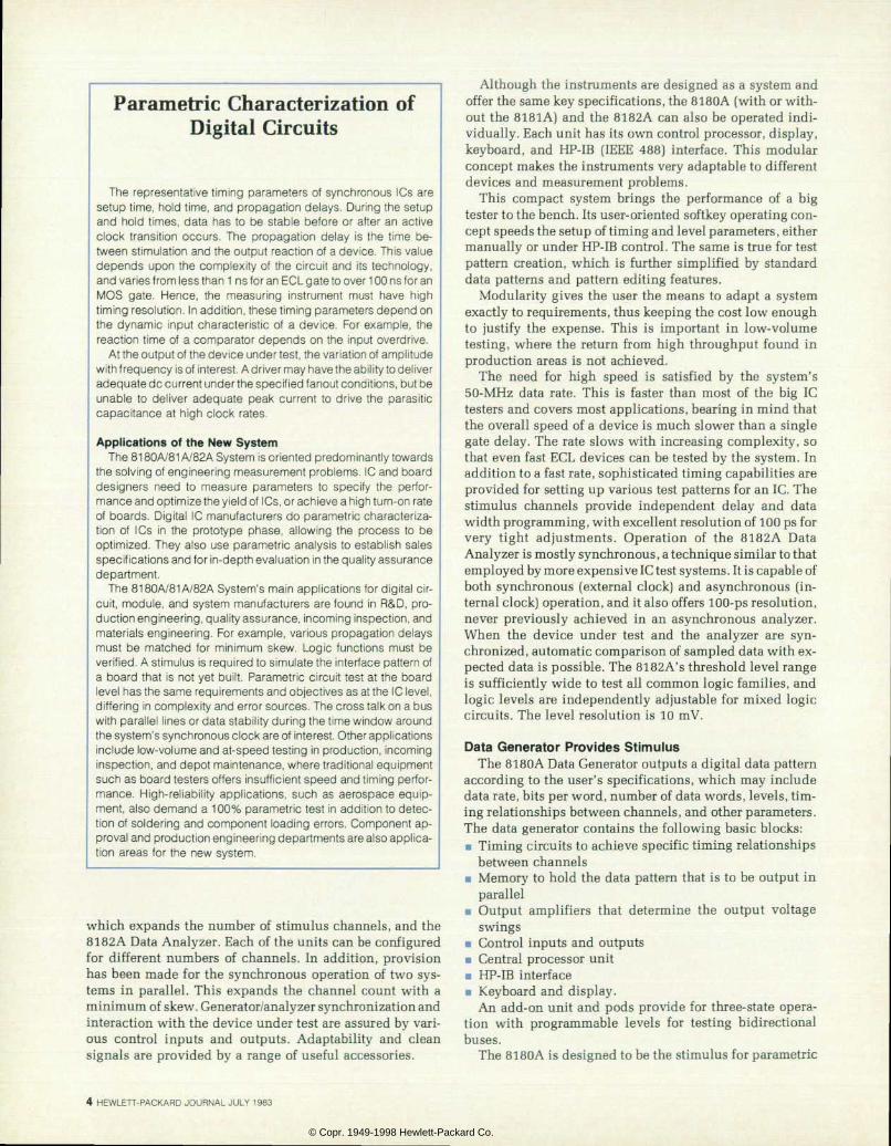
The New Solut ion The new HP 8180A/81A/82A Stimulus/Response System
(Fig. 1) provides an answer to the new requirements. It offers both device stimulation and response analysis, and consists of the 8180A Data Generator, the 8181A Extender,
Fig. 1 . The 81 80 A Data Generator (top left), the 81 81 A Extender (not s h o w n ) , a n d t h e 8 1 8 2 A D a t a A n a l y z e r ( b o t t o m l e f t ) p r o v i d e h i g h - p e r f o r m a n c e , e a s y - t o - u s e , e c o n o m i c a l a t - s p e e d t e s t i n g f o r digi tal integrated circui ts, boards, and modules . The sys tem can be contro l led by a desktop computer (r ight) via the HP-IB (IEEE 488).
JULY 1983 HEWLETT-PACKARD JOURNALS
© Copr. 1949-1998 Hewlett-Packard Co.
Parametric Characterization of Digital Circuits
The representat ive t iming parameters of synchronous ICs are setup t ime, hold t ime, and propagat ion delays. Dur ing the setup and ho ld t imes , da ta has to be s tab le be fore o r a f te r an ac t i ve c l o c k b e o c c u r s . T h e p r o p a g a t i o n d e l a y i s t h e t i m e b e tween st imulat ion and the output react ion of a device. This value depends upon the complex i ty o f the c i rcu i t and i t s techno logy , and varies from less than 1 ns for an ECL gate to over 1 00 ns for an M O S g a t e . H e n c e , t h e m e a s u r i n g i n s t r u m e n t m u s t h a v e h i g h t iming resolut ion. In addit ion, these t iming parameters depend on the dynamic inpu t charac te r i s t i c o f a dev ice . For example , the react ion t ime of a comparator depends on the input overdr ive .
At the output of the device under test, the variation of amplitude with del iver is of interest . A dr iver may have the abi l i ty to del iver adequate dc current under the specif ied fanout condit ions, but be unab le to de l i ve r adequa te peak cu r ren t to d r i ve the pa ras i t i c capac i tance a t h igh c lock ra tes .
Appl icat ions of the New System The 8180A/81 A/82A System is or iented predominantly towards
the solv ing of engineer ing measurement problems. 1C and board d e s i g n e r s n e e d t o m e a s u r e p a r a m e t e r s t o s p e c i f y t h e p e r f o r mance rate optimize the yield of ICs, or achieve a high turn-on rate o f boards. Dig i ta l 1C manufacturers do parametr ic character iza t i on o f ICs i n the p ro to type phase , a l l ow ing the p rocess to be opt imized. They a lso use parametr ic analys is to establ ish sa les specif ications and for in-depth evaluation in the quali ty assurance depar tment .
The 8180A/81A/82A System's main appl icat ions for d ig i ta l c i r cu i t , modu le , and sys tem manufac turers are found in R&D, pro duct ion engineering, qual i ty assurance, incoming inspect ion, and mater ia ls engineer ing. For example, var ious propagat ion delays mus t be ma tched f o r m in imum skew . Log i c f unc t i ons mus t be veri f ied. A st imulus is required to simulate the interface pattern of a board that is not yet bu i l t . Parametr ic c i rcu i t test a t the board level has the same requirements and objectives as at the 1C level, di f fer ing in complexity and error sources. The cross talk on a bus with around l ines or data stabi l i ty dur ing the t ime window around the system's synchronous clock are of interest. Other applications include low-volume and at-speed test ing in product ion, incoming inspect ion, and depot maintenance, where t radi t ional equipment such perfor board testers offers insufficient speed and timing perfor mance . H igh - re l i ab i l i t y app l i ca t ions , such as ae rospace equ ip ment , a lso demand a 100% parametr ic tes t in add i t ion to detec t ion ap so lder ing and component load ing er rors . Component ap proval and product ion engineer ing departments are a lso appl ica t ion areas for the new system.
which expands the number of stimulus channels, and the 8 182 A Data Analyzer. Each of the units can be configured for different numbers of channels. In addition, provision has been made for the synchronous operation of two sys tems in parallel. This expands the channel count with a minimum of skew. Generator/analyzer synchronization and interaction with the device under test are assured by vari ous control inputs and outputs. Adaptability and clean signals are provided by a range of useful accessories.
Although the instruments are designed as a system and offer the same key specifications, the 8180A (with or with out the 8181A) and the 8182A can also be operated indi vidually. Each unit has its own control processor, display, keyboard, and HP-IB (IEEE 488) interface. This modular concept makes the instruments very adaptable to different devices and measurement problems.
This compact system brings the performance of a big tester to the bench. Its user-oriented softkey operating con cept speeds the setup of timing and level parameters, either manually or under HP-IB control. The same is true for test pattern creation, which is further simplified by standard data patterns and pattern editing features.
Modularity gives the user the means to adapt a system exactly to requirements, thus keeping the cost low enough to justify the expense. This is important in low-volume testing, where the return from high throughput found in production areas is not achieved.
The need for high speed is satisfied by the system's 50-MHz data rate. This is faster than most of the big 1C testers and covers most applications, bearing in mind that the overall speed of a device is much slower than a single gate delay. The rate slows with increasing complexity, so that even fast ECL devices can be tested by the system. In addition to a fast rate, sophisticated timing capabilities are provided for setting up various test patterns for an 1C. The stimulus channels provide independent delay and data width programming, with excellent resolution of 100 ps for very tight adjustments. Operation of the 8182A Data Analyzer is mostly synchronous, a technique similar to that employed by more expensive 1C test systems . It is capable of both synchronous (external clock) and asynchronous (in ternal clock) operation, and it also offers 100-ps resolution, never previously achieved in an asynchronous analyzer. When the device under test and the analyzer are syn chronized, automatic comparison of sampled data with ex pected data is possible. The 8182A's threshold level range is sufficiently wide to test all common logic families, and logic levels are independently adjustable for mixed logic circuits. The level resolution is 10 mV.
Data Generator Provides St imulus The 8180A Data Generator outputs a digital data pattern
according to the user's specifications, which may include data rate, bits per word, number of data words, levels, tim ing relationships between channels, and other parameters. The data generator contains the following basic blocks: • Timing circuits to achieve specific timing relationships
between channels • Memory to hold the data pattern that is to be output in
parallel • Output amplifiers that determine the output voltage
swings • Control inputs and outputs • Central processor unit • HP-IB interface • Keyboard and display.
An add-on unit and pods provide for three-state opera tion with programmable levels for testing bidirectional buses.
The 8180A is designed to be the stimulus for parametric
4 H E W L E T T - P A C K A R D J O U R N A L J U L Y 1 9 8 3
© Copr. 1949-1998 Hewlett-Packard Co.
hardware analysis. Therefore, it provides precise level and timing capabilities at high speed. This is in contrast to other types of word generators, which often provide data patterns only at low speed, with moderate or no level definition and poor timing capabilities.
The 8180A can be configured as an 8-to-16-channel generator in 4-channel increments. A maximum of eight channels can be R Z (return to zero), that is, having inde pendently programmable delay and width. All other chan nels are NRZ (non return to zero) channels. The channel count can be expanded by using up to two 8181A Extend ers, each with a maximum of 24 NRZ channels with programmable common delay. This configuration provides 64 channels. Synchronous parallel operation doubles this number to 128.
Data Analyzer Measures Response The 8 1 82 A Data Analyzer collects , analyzes , and displays
digital bit patterns. These tasks are performed according to the user's specifications, which may include input thresholds, data qualification, sampling point (the point in time at which data is sampled, referenced to the external clock), compare time window, and other parameters. The 8182A contains the following basic blocks: • Input comparators to determine the states of logic signals
(1, 0, or between high and low thresholds) • Trigger circuits to indicate the beginning or end of data
capture • High-speed memory to store sampled data • Low-speed memory to hold reference data • Timing circuits to determine precisely when data is to be
captured or compared • Control inputs and outputs
• Central processor unit • HP-IB interface • Keyboard and display.
The 8182A Data Analyzer is designed for high-speed functional and parametric hardware analysis of digital cir cuits. The data analyzer can be configured from 8 to 32 channels in 8-channel increments, each channel having identical analyzing capabilities. Synchronous parallel operation doubles the number of channels to a maximum of 64.
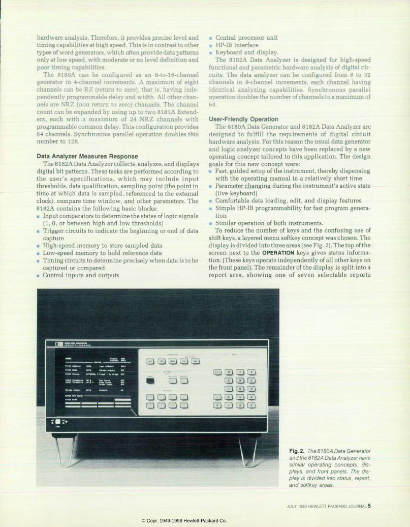
User-Friendly Operation The 8180A Data Generator and 8182A Data Analyzer are
designed to fulfill the requirements of digital circuit hardware analysis. For this reason the usual data generator and logic analyzer concepts have been replaced by a new operating concept tailored to this application. The design goals for this new concept were: • Fast, guided setup of the instrument, thereby dispensing
with the operating manual in a relatively short time a Parameter changing during the instrument's active state
(live keyboard) • Comfortable data loading, edit, and display features • Simple HP-IB programmability for fast program genera
tion « Similar operation of both instruments.
To reduce the number of keys and the confusing use of shift keys, a layered menu softkey concept was chosen. The display is divided into three areas (see Fig . 2) . The top of the screen next to the OPERATION keys gives status informa tion. (These keys operate independently of all other keys on the front panel). The remainder of the display is split into a report area, showing one of seven selectable reports
Fig. 2. The 81 80A Data Generator andthe8182A Data Ana lyzer have s i m i l a r o p e r a t i n g c o n c e p t s , d i s p l ays , and f r on t pane l s . The d i s p lay is d iv ided into status, report , and sof tkey areas.
JULY 1983 HEWLETT-PACKARD JOURNALS
© Copr. 1949-1998 Hewlett-Packard Co.
(parameter settings or data display), and the softkey area containing the entry field, which shows the selected parameter and the labels for the eight softkeys beside the screen. Softkey and report areas can be selected indepen dently or in common by the CALL keys. If the entry field is not activated, the area can be used to extend the data display in the report area. The parameters are selected by the softkeys either directly (e.g., softkey label Cycle Mode to access the cycle mode), or through a softkey tree (e.g., softkeys Trigger and Delay lead to trigger delay). After selec tion, the parameters can be changed either by softkeys or by data keys. Any softkeys that contribute nothing to the cur rent operational status of the instrument are blanked to avoid confusing the user.
This operating concept offers quick access to every parameter, regardless of the contents of the report area.
Similar Operation The 8180A Data Generator and 8182A Data Analyzer are
designed to operate similarly, so that a user who is familiar with one instrument can use the other without a long familiarization time. The keyboards differ in only three keys. Softkeys with the same function for each instrument are labeled identically and occupy the same position on both keyboards (many softkey label sets on both instruments are identical). The pages displayed are very similar, too, with main settings shown on the control page. The timing parameters, which appear on the analyzer's control page, require a page of their own in the generator. The generator's output page corresponds to the analyzer's input page in the same way the 8180A output data page corresponds to the 8182A expected data page.
Both instruments have a miscellaneous page, which in the 8182A also contains store and recall functions. A spe cial feature of the generator is the macro data page, which extends considerably the editing capabilities of the instru ment. The data analyzer has three pages on which to display received data in the form of the state list, the timing diag ram, and an entirely new feature called the error map. The
error map gives a concise overview of the Compare Data result. It displays one dot for each memory location. This dot is replaced by a square if data received differs from expected data. Furthermore, there are special features for the individual masking of any bit or word (see article, page 14).
The expected data page, the state list, and the data page in the 8182A are user-defined. Channels can be deleted from the display or grouped together in segments of up to 16. The channels in each segment can be configured in a manner that is totally independent of their hardware order, en abling the user to assign a code to every segment. It is also possible to display a channel in more than one segment concurrently. The timing diagram offers a full set of fea tures, such as zooming in both horizontal and vertical axes, glitch display, delta measurement, and individual channel arranging.
Special attention was paid to the editing features. The 8180A has memory, line, and channel editing features. Memory editing consists of set and clear functions. Channel editing provides clear, set, counter, PRBS (pseudorandom binary sequence), and copy. Line editing functions include insert, delete, copy, and move. It is also possible to define a set of 16 words (macros) on a special page, and then copy one or more of them to the data memory.
In addition to many of the above features, the 8182A has other analyzer- oriente d editing features for expected data. These include the setting and clearing of masks, and the ability to copy received data to the expected data memory for future comparison.
Live Keyboard For fast parametric measurement it is often. necessary to
change instrument parameters during the measurement phase. In the 8180A this is achieved by changing all analog parameters without disturbing the generator output in any way. If other changes (e.g., output data) are being made, the instrument interrupts the cycle to make the change, and then returns to the point at which the cycle was interrupted.
8 1 SEA
Clock
S t a t u s I B L E
Stored Wor d ï 0£40
T I M I N G D I A G R A M S
Window Display Glitches U h a n n e I U u r s Address 0084
E N T E R M E W V A L U E
Label A
F i g . 3 . W h e n c h a n g i n g m e a s u r e m e n t p a r a m e t e r s d u r i n g a measurement , the d isp lay can be sp l i t in to two areas, one of which shows control page parameters in the sof tkey area. Here the t iming page is d isplayed whi le the probe threshold is be ing changed.
6 HEWLETT-PACKARD JOURNAL JULY 1983
© Copr. 1949-1998 Hewlett-Packard Co.
This operation is performed without disturbing clocks or data. Therefore, the device under test, which contains only combinational and sequential logic, does not recognize the interruption.
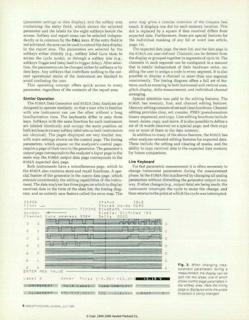
The 8182A Data Analyzer's input thresholds can also be changed during the active cycle (data capture). Other analyzer features facilitate fast measurements. The mi croprocessor displays the received data not only when the instrument stops, but also when the data rate falls below 10 MHz. This is a particularly useful attribute when dealing with slow clock rates or clock bursts. Other instruments usually have to abort a measurement to display the data received. Another useful feature is auto-arming. This al lows the user to preselect the point in time at which the instrument will begin a new measurement, so that the result of any change in the operating condition of the device under test can be displayed immediately.
To ensure that the instrument is operable during a period of processor activity, the keyboard is interrupt-controlled, permitting the storage of up to eight keystrokes until the processor has time to respond to them. When changing measurement parameters during a measurement phase, it is possible to split the display screen into two areas, one showing the report area (perhaps the error map), and the other showing control page parameters in the softkey area. Fig. 3 shows an example; the timing page is displayed while the probe threshold is being changed.
The HP-IB system is designed to give direct access to parameters and a fast instrument response. The mnemonics are easy to remember, avoiding the need to refer to the manual continuously, making programming simple and reducing familiarization time. To program the 8180A to a frequency of 20 MHz, for example, the controller sends the message FRQ 20 MHZ. Where the parameters on each in strument are identical, so are the mnemonics.
For the transfer of high volumes of data from the control ler to the instrument and vice- versa, a binary transfer mode has been implemented. In this mode, every byte on the bus is dedicated to eight bits of data. Data transfer rates of 12,000 bytes per second are achieved, giving a data reload time of less than two seconds for the whole system. This makes it possible to write fast-running programs.
Acknowledgments We would like to thank Roberto Mottola for his outstand
ing contribution in defining the operating concept for both instruments, Horst Link, who was responsible for the mechanical design of all instruments and accessories, Eckhard Hettlage, who designed the displays, Peter Stol- lenmaier, who contributed to the 8182A power supply, Rainer Storn, who helped with the 8182A self-test software, and last but not least, our thanks go to Günter Riebesell and Reinhard Falke for their help and guidance along the way.
A High-Speed Data Generator for Digital Testing by Ulrich Hübner, Werner Berkel, Heinz Nüssle, and Josef Becker
THE NEW HP 8180A DATA GENERATOR represents a significant step forward in the production of high speed data generators. It offers high timing accuracy,
precise pulse-level definition, ease of operation with either manual or remote control , and great flexibility on the bench and in the rack.
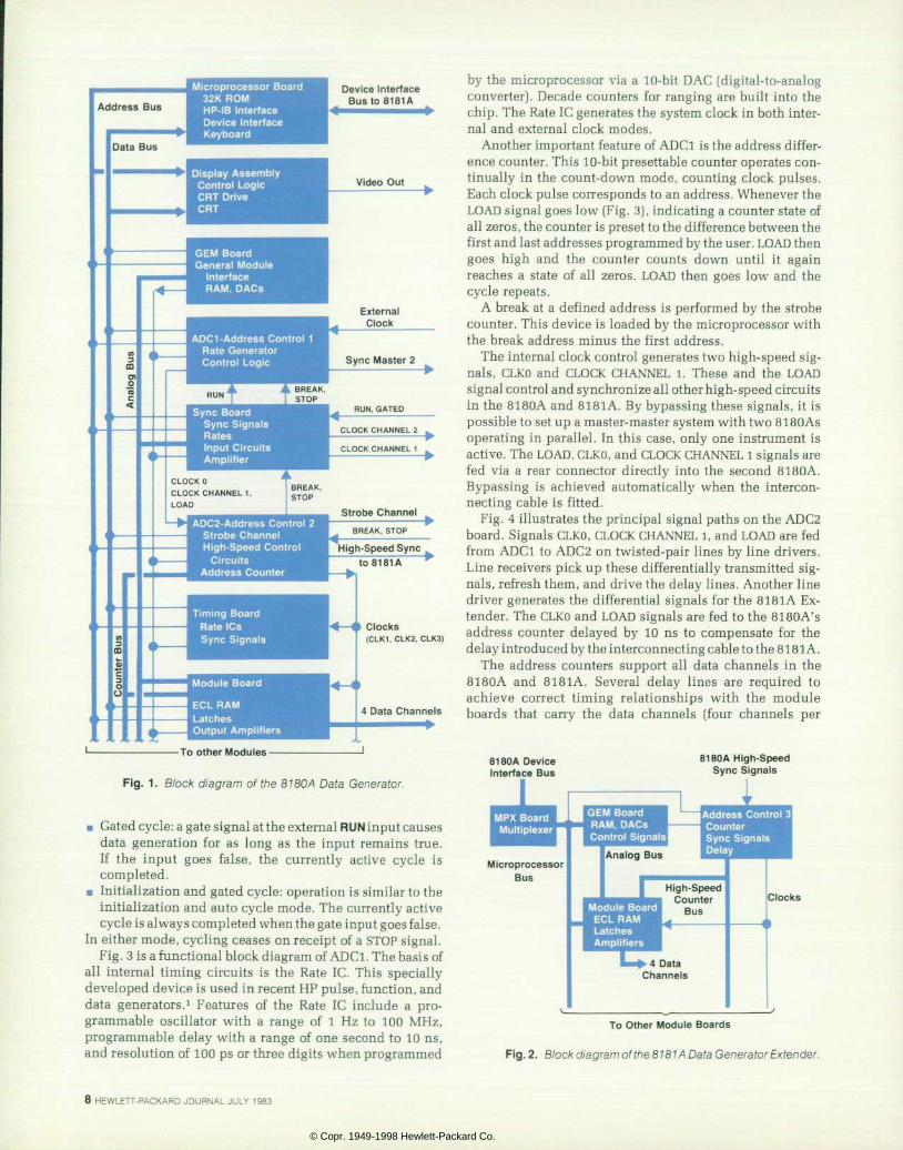
The 8180A consists of a power supply module, a display module, and eleven printed circuit boards, which plug into a motherboard. Fig. 1 illustrates the various functional blocks and main interconnections.
The 81 81 A Data Generator Extender is constructed along the same lines as the 8180A with the exception of the display and keyboard. All control functions are performed by the 8180A, the 8181A being merely a system slave. Fig. 2 is a block diagram of the 8181A.
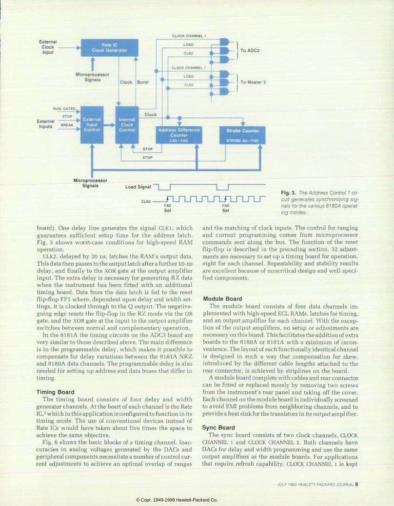
Internal System Organizat ion All high-speed control signals in the 8180A Data
Generator are generated on two boards, designated Address
Control 1 and Address Control 2 (ADCl and ADC2). The logic consists of 10k and 100k ECL devices and is controlled by the central processing unit by way of a high-speed bidirectional bus.
On ADCl, three signals that synchronize the address counters and signals for both clock channels are generated. The board responds to the commands RUN, GATED, STOP, and BREAK. There are three basic operating modes: • Single cycle: a RUN signal starts a single cycle from the
preset first address to the preset last address. • Auto cycle: after a RUN signal, data is generated repeti
tively from the first to the last addresses. • Initialization and auto cycle: a RUN signal starts data
generation at address 0000. Data generation continues to the first address and then cycles between the first and last addresses repetitively.
In these three operating modes, cycling is halted on receipt of a BREAK or STOP signal.
Two further modes are controlled from this board:
JULY 1983 HEWLETT-PACKARD JOURNAL 7
© Copr. 1949-1998 Hewlett-Packard Co.
Address Bus
Data Bus
Microprocessor Board 32K ROM HP-IB Interface Device Interface Keyboard
Display Assembly Control Logic CRT Dr ive CRT
GEM Board General Module
Interface RAM, DACs
Device Interface Busto 81 81 A
Video Out
External Clock
ADC1 -Address Control 1 Rate Generator Control Logic
R U N
Sync Board Sync Signals Rates Input Circuits Amplif ier
CLOCK 0
CLOCK CHANNEL 1,
LOAD
BREAK,
BREAK,
STOP
ADC2-Address Control 2 Strobe Channel High-Speed Control
Circuits Address Counter
T iming Board Rate ICs Sync Signals
Module Board
ECL RAM Latches Output Ampli f iers
Sync Master 2
R U N , G A T E D
CLOCK CHANNEL 2
CLOCK CHANNEL 1
Strobe Channel |
t B R E A K , S T O P
High-Speed Sync to 81 81 A
Clocks ( C L K 1 , C L K 2 , C L K 3 )
4 Data Channels I
-To other Modules -
Fig. 1 . B lock d iagram of the 81 80 A Data Generator .
m Gated cycle: a gate signal at the external RUN input causes data generation for as long as the input remains true. If the input goes false, the currently active cycle is completed.
• Initialization and gated cycle: operation is similar to the initialization and auto cycle mode. The currently active cycle is always completed when the gate input goes false.
In either mode, cycling ceases on receipt of a STOP signal. Fig. 3 is a functional block diagram of ADCl. The basis of
all internal timing circuits is the Rate 1C. This specially developed device is used in recent HP pulse, function, and data generators.1 Features of the Rate 1C include a pro grammable oscillator with a range of 1 Hz to 100 MHz, programmable delay with a range of one second to 10 ns, and resolution of 100 ps or three digits when programmed
by the microprocessor via a 10-bit DAC (digital-to-analog converter). Decade counters for ranging are built into the chip. The Rate 1C generates the system clock in both inter nal and external clock modes.
Another important feature of ADCl is the address differ ence counter. This 10-bit presettable counter operates con tinually in the count-down mode, counting clock pulses. Each clock pulse corresponds to an address. Whenever the LOAD signal goes low (Fig. 3], indicating a counter state of all zeros, the counter is preset to the difference between the first and last addresses programmed by the user. LOAD then goes high and the counter counts down until it again reaches a state of all zeros. LOAD then goes low and the cycle repeats.
A break at a defined address is performed by the strobe counter. This device is loaded by the microprocessor with the break address minus the first address.
The internal clock control generates two high-speed sig nals, CLKO and CLOCK CHANNEL 1. These and the LOAD signal control and synchronize all other high-speed circuits in the 8180A and 8181A. By bypassing these signals, it is possible to set up a master-master system with two 8180As operating in parallel. In this case, only one instrument is active. The LOAD, CLKO, and CLOCK CHANNEL 1 signals are fed via a rear connector directly into the second 8180A. Bypassing is achieved automatically when the intercon necting cable is fitted.
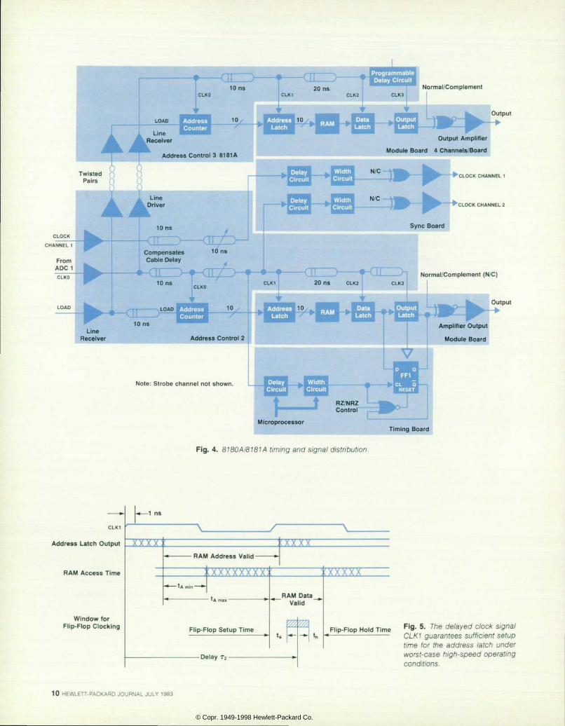
Fig. 4 illustrates the principal signal paths on the ADC2 board. Signals CLKO, CLOCK CHANNEL 1, and LOAD are fed from ADCl to ADC2 on twisted-pair lines by line drivers. Line receivers pick up these differentially transmitted sig nals, refresh them, and drive the delay lines. Another line driver generates the differential signals for the 8181A Ex tender. The CLKO and LOAD signals are fed to the 81 80 A' s address counter delayed by 10 ns to compensate for the delay introduced by the interconnecting cable to the 8181 A.
The address counters support all data channels in the 8180A and 8181A. Several delay lines are required to achieve correct timing relationships with the module boards that carry the data channels (four channels per
8180A Device Interface Bus
8180A High-Speed Sync Signals
Clocks
To Other Module Boards
Fig. 2. Block diagram of the 81 81 A Data Generator Extender.
8 H E W L E T T - P A C K A R D J O U R N A L J U L Y 1 9 8 3
© Copr. 1949-1998 Hewlett-Packard Co.
C L O C K C H A N N E L 1
External Clock Input
Rate 1C Clock Generator To ADC2
Microprocessor Signals
Load Signal
FAD Set
board). One delay line generates the signal CLKi, which guarantees sufficient setup time for the address latch. Fig. 5 shows worst-case conditions for high-speed RAM operation.
CLK2, delayed by 20 ns, latches the RAM's output data. This data then passes to the output latch after a further 10-ns delay, and finally to the XOR gate at the output amplifier input. The extra delay is necessary for generating R Z data when the instrument has been fitted with an additional timing board. Data from the data latch is fed to the reset flip-flop FFl where, dependent upon delay and width set tings, it is clocked through to the Q output. The negative- going edge resets the flip-flop in the RZ mode via the OR gate, and the XOR gate at the input to the output amplifier switches between normal and complementary operation.
In the 8181A the timing circuits on the ADC3 board are very similar to those described above. The main difference is in the programmable delay, which makes it possible to compensate for delay variations between the 8181A NRZ and 8180A data channels. The programmable delay is also needed for setting up address and data buses that differ in timing.
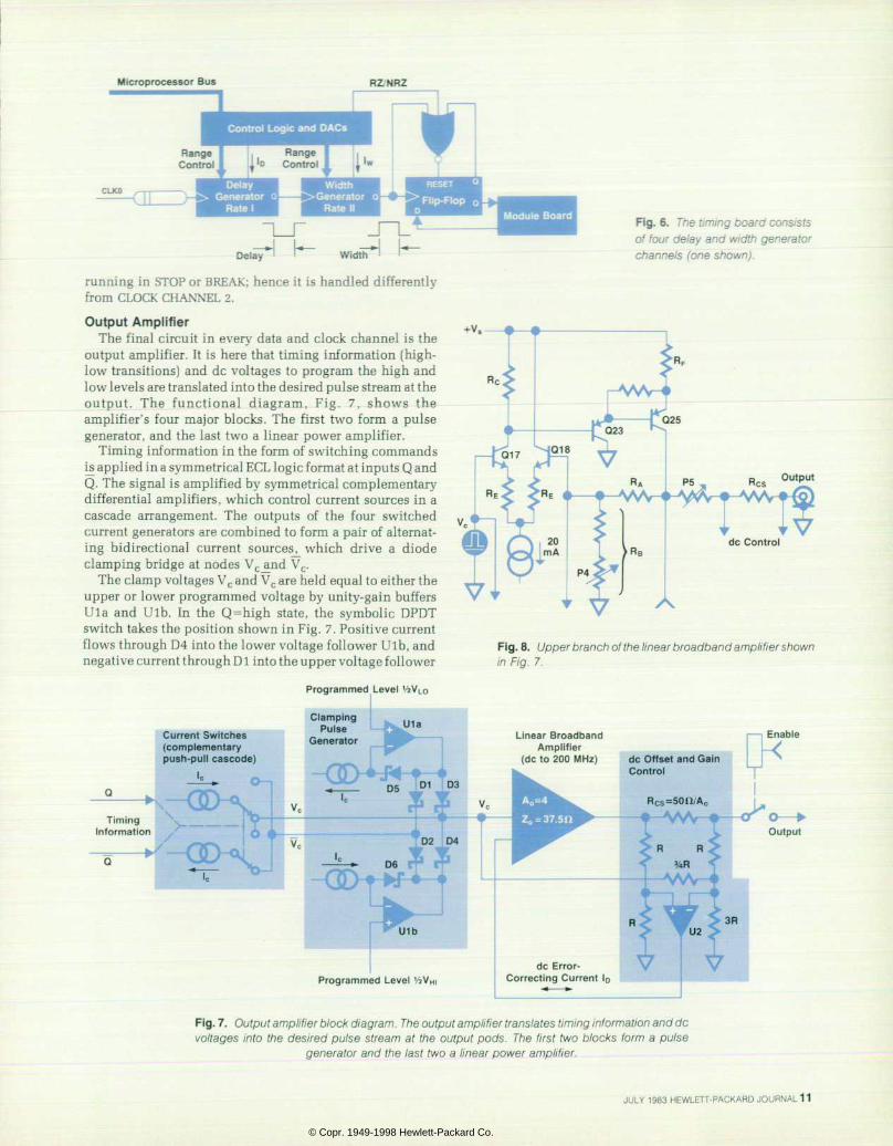
Timing Board The timing board consists of four delay and width
generator channels. At the heart of each channel is the Rate 1C,1 which in this application is configured to function in its timing mode. The use of conventional devices instead of Rate ICs would have taken about five times the space to achieve the same objective.
Fig. 6 shows the basic blocks of a timing channel. Inac curacies in analog voltages generated by the DACs and peripheral components necessitate a number of control cur rent adjustments to achieve an optimal overlap of ranges
F A D Set
Fig . 3 . The Address Cont ro l 1 c i r cu i t genera tes synchron iz ing s ig nals for the var ious 8780/4 operat ing modes.
and the matching of clock inputs. The control for ranging and current programming comes from microprocessor commands sent along the bus. The function of the reset flip-flop is described in the preceding section. 32 adjust ments are necessary to set up a timing board for operation, eight for each channel. Repeatability and stability results are excellent because of noncritical design and well speci fied components.
Module Board The module board consists of four data channels im
plemented with high-speed ECL RAMs, latches for timing, and an output amplifier for each channel. With the excep tion of the output amplifiers, no setup or adjustments are necessary on this board. This facilitates the addition of extra boards to the 8180A or 8181A with a minimum of incon venience. The layout of each functionally identical channel is designed in such a way that compensation for skew, introduced by the different cable lengths attached to the rear connector, is achieved by striplines on the board.
A module board complete with cables and rear connector can be fitted or replaced merely by removing two screws from the instrument's rear panel and taking off the cover. Each channel on the module board is individually screened to avoid EMI problems from neighboring channels, and to provide a heat sink for the transistors in its output amplifier.
Sync Board The sync board consists of two clock channels, CLOCK
CHANNEL 1 and CLOCK CHANNEL 2. Both channels have DACs for delay and width programming and use the same output amplifiers as the module boards. For applications that require refresh capability, CLOCK CHANNEL 1 is kept
JULY 1983 HEWLETT-PACKARD JOURNALS
© Copr. 1949-1998 Hewlett-Packard Co.
P r o g r a m m a b l e D e l a y C i r c u i t
N o r m a l / C o m p l e m e n t
O u t p u t
O u t p u t A m p l i f i e r
M o d u l e B o a r d 4 C h a n n e l s / B o a r d A d d r e s s C o n t r o l 3 8 1 8 1 A
T w i s t e d ' Pa i rs
C o m p e n s a t e s 1 0 n s C a b l e D e l a y
Normal /Complement (N/C)
Ampl i f ie r Output
Module Board A d d r e s s C o n t r o l 2
O u t p u t
N o t e : S t r o b e c h a n n e l n o t s h o w n .
M i c r o p r o c e s s o r
Fig . 4 . 8180A/8181A t iming and s igna l d is t r ibu t ion.
T i m i n g B o a r d
C L K 1
A d d r e s s L a t c h O u t p u t
R A M A c c e s s T i m e
W i n d o w f o r F l i p - F l o p C l o c k i n g
U— 1 ns
xx xx : ( X X X X R A M A d d r e s s V a l i d -
(xxxxxxxx: : - t A m i n -
( X X X X X
R A M D a t a V a l i d
-De lay T2
F l i p - F l o p H o l d T i m e F i 9 ' 5 ' T h e d e l a y e d C l o c k S ' 9 n a l CLK1 guarantees suf f ic ient setup t ime fo r t he add ress l a t ch unde r wors t -case h igh-speed opera t ing condit ions.
1 0 H E W L E T T - P A C K A R D J O U R N A L J U L Y 1 9 8 3
© Copr. 1949-1998 Hewlett-Packard Co.
Microprocessor Bus
Range Control
R Z N R Z
Delay G e n e r a t o r o
Rate I
Delay
Width > Generator o
Rate II
Width
' F l ip-Flop Q Module Board Fig. 6 . The t iming board cons is ts
o f four de lay and width generator channels (one shown).
running in STOP or BREAK; hence it is handled differently from CLOCK CHANNEL 2.
Output Ampli f ier The final circuit in every data and clock channel is the
output amplifier. It is here that timing information (high- low transitions) and dc voltages to program the high and low levels are translated into the desired pulse stream at the output. The functional diagram, Fig. 7, shows the amplifier's four major blocks. The first two form a pulse generator, and the last two a linear power amplifier.
Timing information in the form of switching commands is applied in a symmetrical ECL logic format at inputs Q and Q. The signal is amplified by symmetrical complementary differential amplifiers, which control current sources in a cascade arrangement. The outputs of the four switched current generators are combined to form a pair of alternat ing bidirectional current sources^ which drive a diode clamping bridge at nodes Vc_and Vc.
The clamp voltages Vc and Vc are held equal to either the upper or lower programmed voltage by unity-gain buffers Ula and Ulb. In the Q=high state, the symbolic DPDT switch takes the position shown in Fig. 7. Positive current flows through D4 into the lower voltage follower Ulb, and negative current through D 1 into the upper voltage follower
Programmed Level 1/2VLo
A - e s WVH HyA-f^ArVf©
dc Control
. A .
Fig. 8. Upper branch of the l inear broadband ampl i f ier shown in Fig. 7.
Current Switches (complementary push-pull cascode)
Clamping Pulse
Generator Linear Broadband Amplif ier
(dc to 200 MHz) dc Offset and Gain Control
dc Error- Correcting Current ID Programmed Level ' /2VH
Fig. translates information amplifier block diagram. The output amplifier translates timing information and dc vo l tages in to the des i red pu lse s t ream a t the ou tpu t pods . The f i rs t two b locks fo rm a pu lse
generator and the last two a l inear power ampl i f ier .
JULY 1983 HEWLETT-PACKARD JOURNAL 11
© Copr. 1949-1998 Hewlett-Packard Co.
Ula. As long as Vra>VLO with at least 0.5V difference, D3 and D2 may be regarded as switched off.
Two more diodes, D5 and D6, compensate for the on voltages and temperature dependence of D3 and D4. All diodes are supplied with equal currents (Ic=15 mA). Minor differences in forward voltage drop and series resistance of the matched pairs D3, D5 and D4, D6 are corrected by trimmers. Thus Vc is equal to exactly V^V^ when D4 is con ducting (Q=high), and V2VLO when D3 is conducting. A small error because of junction temperature differences re mains in D 3 and D4 when they are switched on or off. Schottky-barrier diodes are chosen for fast switching with out storage delay.
The second clamping node, Vc, provides a complemen tary pulse train to Vc. This is used for two dynamic pur poses. To accelerate the high-low transitions of Vc, Vc is high-pass coupled to the bases of switched current-source transistors. The result of this additional drive is that the voltage transitions of Vc are more like pulses with constant rise time than the natural constant-slope behavior of a current-steered voltage clamp.
The second purpose of the Vc branch is to provide con stant current loading for voltage-followers Ula and Ulb. If Dl and D2 were not present, these op-amps would be re quired to deliver pulsed output currents. Frequency re sponse limitations within the op-amps would lead to duty- cycle-dependent level variations in some critical high- frequency regions. The symmetrical clamping bridge draws dc current from Ula and Ulb, keeping pulse tops flat from dc to the nanosecond region.
The clamp output signal Vc is amplified to the desired amplitude and power by a class-A push-pull amplifier. In Fig. 8, only the upper half of the amplifier, with compo nents determining gain A0 and output impedance Z0, is shown. The complementary symmetrical lower branch completes the amplifier for dc operation, and acts as a doubler for overall transconductance and output current. This basic arrangement is noninverting.
Minor aberrations and tolerances are trimmed out with
Table I Data Generator Output Ampl i f ier Performance
P r o g r a m m e d l o a d f r o m S O U i n t o 5 0 1 1 f r o m S O U i n t o h i g h c o n d i t i o n ( v o l t a g e s d o u b l e i f i m p e d a n c e ( - 1 0 k i l )
no load connected)
High level range
Low level range Resolution
Ampli tude range Level accuracy after
Level accuracy after
Transition time
Typical transition t ime for ECL levels (20%-80%) Preshoot , Over shoot, Ringing
-1.5V to +5.5V
-2.0V to +5.0V
3 digits (best case 10 mV)
0.5V to 5.5V
20 ns sett l ing t ime ±0.5% of level ±3% of amplitude ±30 mV (add ±30 mV for amplitudes >0.7V)
1 ms settl ing time ±0.5% of level ±30 mV (add ±30 mV for amplitudes <0.7V)
<3.0 ns + | amplitude j xo. 2 ns
1.5 ns
-1.0V to +17.0V
-2.0V to +16. 0V
3 digits (best case 20 mV)
1.0V to 17.0V
40 ns sett l ing t ime ±0.5% of level ±3% of amplitude ±30 mV (add ±30 mV for amplitudes
1 ms settl ing time ±0.5% of level ±60 mV (add ±60 mV for amplitudes <1.5V)
<3.0 ns + ¡amplitude! X0-5 ns
<±10% of amplitude <±10% of amplitude
P4, for the amplifier unloaded, and again with P5, after connection of a 50 fi load.
Output amplifiers commonly found in pulse and data generators are usually designed as current or voltage sources, both needing an internal 50ÃÃ load to present the
* * â € ” 1 I I t 1 I '
F i g . 9 . T h e t r i - s t a t e p o d m a k e s t h e d a t a g e n e r a t o r o u t p u t s c o m pat ib le w i th b id i rec t iona l bus and I /O pin configurat ions. The control and power unit on top of the 81 80A Data Generator is par t o f the pod system.
1 2 H E W L E T T - P A C K A R D J O U R N A L J U L Y 1 9 8 3
© Copr. 1949-1998 Hewlett-Packard Co.
correct Z0 (50fi) at their output. The amplifier concept used here gives well-defined gain and output impedance with out wasting 50% of the ac power on an internal 50ft ballast. This is important in generators in which many data chan nels are packed closely together, like the 8180A and 8181 A.
Internal feedback in even' amplifier stage (RE,RF) helps ensure stability and allows the use of full circuit speed (speed is ultimately limited by the propagation delay around the feedback loop in the amplifier network). The free-running amplifier produces an output signal with the specified accuracy. A dc offset of up to several hundred millivolts reflecting the thermal history of linearly operat ing transistors may appear, however. A dc error can also be introduced by varying the supply voltages to accommodate different output amplitude requirements. To eliminate these offsets, an additional dc control loop checks the out put voltage and the output current simultaneously and en sures precise operation under any loading, level, or supply conditions.
To understand the operation of this dc control loop, look at the inputs of error amplifier U 2 in Fig. 7. At the nonin- verting input, a voltage V+ =V2(V0+RCSI0) is compared with V~=y2Vc+3/8V0 at the inverting input. The op-amp forces a corrective current into the inverting input of the main amplifier to keep V + -V~=0. The dc precision now depends on the op-amp quality and the ratio of the resistors in the voltage divider. When V + -V~=0, then V0+RCSI0 = Vc+3/4V0. Since A0=4 and RCg=50il/A0, this expression
becomes V4V0+(50il/A0)I0=Vc, or V0=A0Vc-(50n)I0, which describes a linear amplifier with voltage gain A0 and an output impedance of 50O.
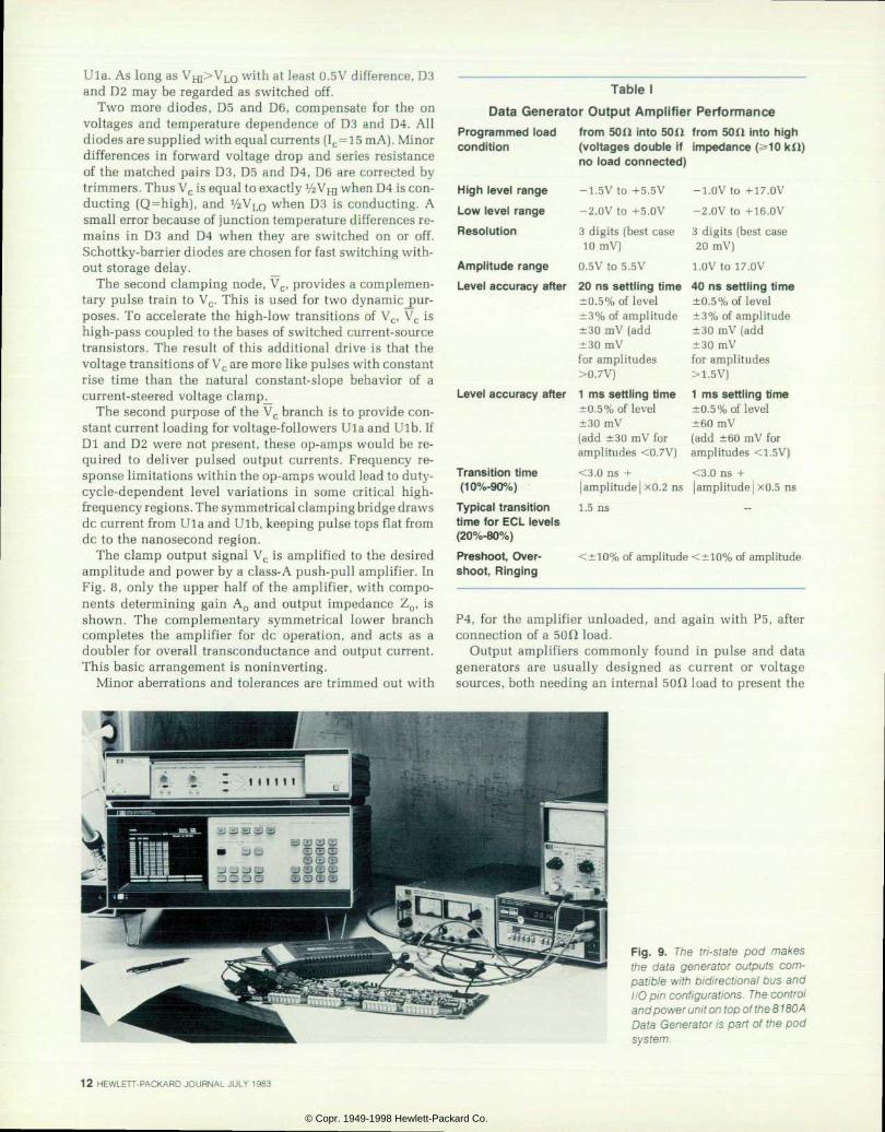
Table I shows the principal specifications of the output amplifier.
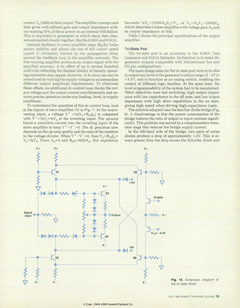
Tri-State Pod The tri-state pod is an accessory to the 8180A Data
Generator and 8181A Extender. Its function is to make the generator outputs compatible with bidirectional bus and I/O pin configurations.
The main design aims for the tri-state pod were to be able to output any level in the generator's output range of -2V to + 5. 5V, and to function as an analog switch, enabling the control of different logic families. At the same time, the level programmability of the system had to be maintained. Other objectives were fast switching, high output imped ance with low capacitance in the off state, and low output impedance with high drive capabilities in the on state, giving high speed when driving high-capacitance loads.
The solution adopted uses the familiar diode bridge (Fig. 9). A disadvantage is that the power consumption of the bridge reduces the ratio of output to input currents signifi cantly. This problem was solved by a complementary trans istor stage that reduces the bridge supply current.
In the left-hand side of the bridge, two pairs of series diodes produce a drop of approximately 1.4V. This is al ways greater than the drop across the Schottky diode and
Signal Input
H - H T A V V H *
V - V - F i g . 1 0 . S c h e m a t i c d i a g r a m o f the tr i-state driver.
JULY 1983 HEWLETT-PACKARD JOURNAL 13
© Copr. 1949-1998 Hewlett-Packard Co.
the emitter junction of the output transistor in each line. The series Schottky-diode-resistor configuration, in com bination with an offset adjustment, permits the use of un matched components without a reduction in level accu racy. When the enable voltage meets or rises above the -4.30V threshold, transistors Q5 and Q6 begin to conduct, thereby turning Ql and Q2 off. In this way, the bridge
becomes reverse-biased, with the clamping diodes ensur ing that the output circuit is cut off when the voltage at the output is in the range -2V to +5. 5V.
Reference 1. C. for et al, "Designing Bipolar Integrated Circuits for a Pulse/Function Generator Family," Hewlett-Packard Journal, Vol. 34, no. 6, June 1983.
High-Speed Data Analyzer Tests Threshold and Timing Parameters by Dieter Kible, Bernhard Roth, Martin Dietze, and Ulrich Schòttmer
CONVENTIONAL DATA ANALYZERS fall generally into two categories. First, there are the high-speed asynchronous timing analyzers, which produce test
results similar to an oscilloscope on several channels. These analyzers are used mainly for functional analysis of random logic. Second, there are the synchronous state analyzers , which are used mostly for the functional analysis of microprocessor-based systems with real-time or other complex sequential logic. Parametric measurements, on the other hand, have to be made with oscilloscopes or timing analyzers having fairly coarse time resolution (the fastest timing analyzers available offer only 1.5 to 2 ns resolution, with a significant additional error because of skew between data channels).
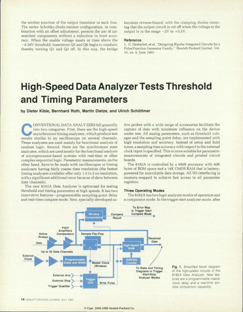
The new 8182A Data Analyzer is optimized for testing threshold and timing parameters at high speeds. It has two innovative features — programmable sampling-point delay and real-time compare mode. New, specially-developed ac-
C o m p a r e
tive probes with a wide range of accessories facilitate the capture of data with minimum influence on the device under test. All analog parameters, such as threshold volt ages and the sampling point delay, are implemented with high resolution and accuracy. Instead of setup and hold times, a sampling time accuracy with respect to the external clock input is specified. This is more suitable for parametric measurements of integrated circuits and printed circuit boards.
The 8182A is controlled by a 6809 processor with 40K bytes of ROM space and a 14K CMOS RAM that is battery- powered for nonvolatile data storage. All I/O interfacing is memory-mapped to achieve fast access to all parameter registers.
Three Operat ing Modes The 8182 A has two logic analyzer modes of operation and
a comparator mode. In the trigger start analyzer mode, after
To Error Map in Trigger Start Compare Mode
External Arm
External Stop
Trigger Qualif ier
To State and Timing Diagrams in Trigger
Start/Stop Analyzer Modes
F ig . 1 . S imp l i f i ed b lock d iag ram o f t he h igh -speed c i r cu i t s o f t he 8 7 8 2 A D a t a A n a l y z e r . N e w f e a tures are a programmable master c l o c k d e l a y a n d a r e a l - t i m e w i n dow compar ison capab i l i t y .
1 4 H E W L E T T - P A C K A R D J O U R N A L J U L Y 1 9 8 3
© Copr. 1949-1998 Hewlett-Packard Co.
recognizing a trigger condition, the 8182A begins to accept data into its high-speed memory. Stored data can be dis played as either state or timing diagrams, during or after completion of the measurement cycle. The microprocessor compares the received data with stored expected data and displays comparison failures on the state diagram or a con centrated overview in the error map.
In the trigger stop analyzer mode, after arming , the 8 182 A is always active, that is, it continually accepts data, filling and overwriting its high-speed memory . After recognition of a trigger event, it stops accepting data (after a selectable delay) and displays the previously stored data. Hence the events preceding and following the trigger event can be recorded. The monitoring capabilities are the same as in the trigger start analyzer mode.
The third mode, the trigger start compare mode, is an entirely new feature. It permits a real-time comparison of incoming data with a prestored data pattern contained in the high-speed memory. This comparison takes place dur ing a time window synchronous with the clock input. The window is defined by a delay and a width. Every failure during the compare window generates a high logic level at a rear-panel output, and an error report can be displayed on the error map. Either one-shot or continuous cyclical mea surements are possible.
Hardware Architecture With the exception of the power supply, the display, and
the microprocessor section, the 8182A hardware is to a high degree implemented with ECL to achieve 50-MHz opera tion and high timing accuracy. The eight-channel version of the 8182A contains two boards with digital control cir cuits, one board of clock generators, two boards containing the microprocessor and its interfacing , and two data boards, each with 4 channels. Six more data boards can be plugged into the remaining slots, extending the 8182A up to 32 channels. Fig. 1 shows a simplified block diagram of the hardware.
F i g . 2 . H i g h - i m p e d a n c e , h i g h - f r e q u e n c y , d u a l - t h r e s h o l d p r o b i n g i s p r o v i d e d b y a s p e c i a l t h i c k - f i l m h y b r i d p r o b e circuit.
What Is Window Comparison?
When the 8182A Data Analyzer ¡s in either of its logic analyzer modes, performing l ike a conventional analyzer, i t samples a data s t ream on a po in t -by-po in t bas is . Whatever is present between two samp l i ng even ts can be ana l yzed w i t h t he a id o f a g l i t ch de tec to r , bu t i t i s imposs ib le to de te rmine whether a g l i t ch ap peared at the beginn ing or end of a sampl ing per iod. S imi lar ly , de termin ing the s tab i l i t y o f a log ic leve l dur ing any par t o f the sampling period ¡s also a problem.
I n com ing Da ta
S to red Da ta Pa t te rn C o m p a r e R e s u l t
CLK1 (Window Pulse)
F ig . 1 . In compara to r mode , the 8182A Da ta Ana lyze r com pares incoming data with stored data dur ing a t ime window of p rogrammable w id th .
How can the status of data on a microprocessor bus be deter mined during the period beginning 50 ns before and ending 1 0 ns af ter a c lock edge?
When the 81 82A ¡s operating in its comparator mode, a periodic t ime window can be programmed. Dur ing th is t ime, the incoming data can be compared with an internal ly stored pattern. The t ime window ¡s synchronous wi th the c lock connected to the 8182A c lock probe.
The compar ison c i rcu i t consis ts of an XOR gate in each chan nel, which compares the incoming data with a f ixed data pattern. A pulse of the desired window width (60 ns in the example given here) is appl ied to the enable input of the gate (see Fig. 1) .
Fig. 2 shows the gate output. It is assumed that the stored data pat tern consis ts of low levels , so an Incoming h igh generates a positive pulse at the gate output while the window pulse ¡s high. In Fig. 2a and 2b a fai lure ¡s recognized. Fig. 2c and 2d are border l i ne . The compare e r ro r may no t be recogn ized , a l though one
< 4 n s < 4 n s
LK1 (Window Pulse)
I n c o m i n g D a t a - S
C o m p a r e Result <
(b) (c)
Fig. 2 . Assuming that the s tored data pat tern cons is ts o f a l l low levels, an incoming high level during the window causes a posi t ive compare resul t . Fai lures (a) and (b) are easi ly recog n ized, whi le cases (c) and (d) are border l ine.
edge o f t he Incoming da ta l i es w i th in the t ime w indow. A t t he 8182A input , the incoming data edge must be wi th in 4 ns of the w indow edge for an er ror to be d iagnosed cor rec t ly .
-Mart in Dietze
JULY 1983 HEWLETT-PACKARD JOURNAL 15
© Copr. 1949-1998 Hewlett-Packard Co.
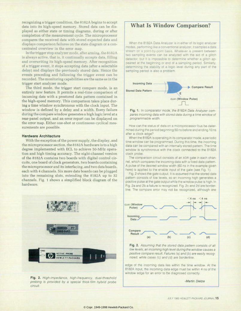
Act ive Probes and Input Ampl i f iers To achieve the design goals of high-impedance, low-
capacitance probing with high-frequency and dual- threshold capabilities, a special active probe circuit was developed. It is realized as a thick-film hybrid circuit (Fig. 2).
The dimensions of the hybrid are 29.7 mm x 10 mm x 2.4 mm. Special care had to be taken in designing the high- impedance input stage layout to achieve the small input capacitance of less than 7 pF (the hybrid alone has only a 4.5-pF input capacitance). The hybrid is packaged in a small aluminum case and connected to a special 1.5-m cable consisting of two shielded cables, one of which is 50Ã1 coax, and two single wires for power and compensation f or ground potential differences. Four of these active probes and cables share a single connector, which can be con nected to the rear panel of the instrument.
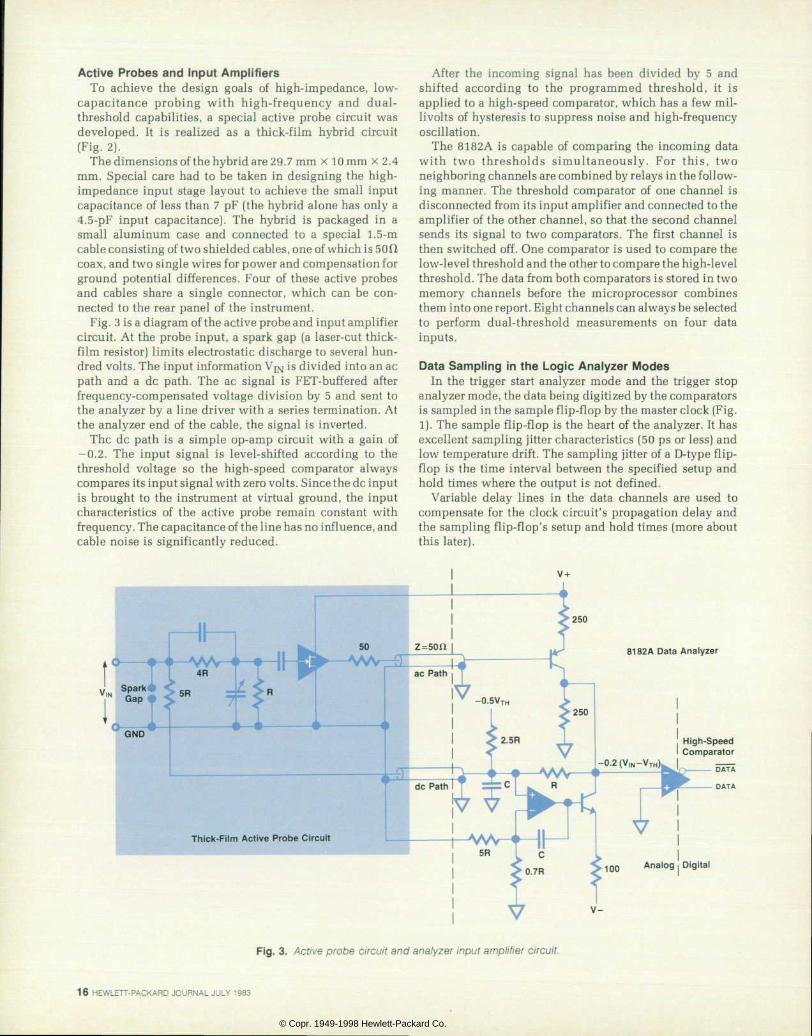
Fig. 3 is a diagram of the active probe and input amplifier circuit. At the probe input, a spark gap (a laser-cut thick- film resistor) limits electrostatic discharge to several hun dred volts. The input information VIN is divided into an ac path and a dc path. The ac signal is FET-buffered after frequency-compensated voltage division by 5 and sent to the analyzer by a line driver with a series termination. At the analyzer end of the cable, the signal is inverted.
The dc path is a simple op-amp circuit with a gain of -0.2. The input signal is level-shifted according to the threshold voltage so the high-speed comparator always compares its input signal with zero volts. Since the dc input is brought to the instrument at virtual ground, the input characteristics of the active probe remain constant with frequency. The capacitance of the line has no influence, and cable noise is significantly reduced.
After the incoming signal has been divided by 5 and shifted according to the programmed threshold, it is applied to a high-speed comparator, which has a few mil livolts of hysteresis to suppress noise and high-frequency oscillation.
The 8 182 A is capable of comparing the incoming data with two thresholds simultaneously. For this, two neighboring channels are combined by relays in the follow ing manner. The threshold comparator of one channel is disconnected from its input amplifier and connected to the amplifier of the other channel, so that the second channel sends its signal to two comparators. The first channel is then switched off. One comparator is used to compare the low-level threshold and the other to compare the high-level threshold. The data from both comparators is stored in two memory channels before the microprocessor combines them into one report. Eight channels can always be selected to perform dual-threshold measurements on four data inputs.
Data Sampl ing in the Logic Analyzer Modes In the trigger start analyzer mode and the trigger stop
analyzer mode, the data being digitized by the comparators is sampled in the sample flip-flop by the master clock (Fig. 1). The sample flip-flop is the heart of the analyzer. It has excellent sampling jitter characteristics (50 ps or less) and low temperature drift. The sampling jitter of a D-type flip- flop is the time interval between the specified setup and hold times where the output is not defined.
Variable delay lines in the data channels are used to compensate for the clock circuit's propagation delay and the sampling flip-flop's setup and hold times (more about this later).
v +
81 82A Data Analyzer
High-Speed Comparator
Thick-Fi lm Active Probe Circuit
Digi tal
V -
Fig. 3 . Act ive probe c i rcu i t and analyzer input ampl i f ie r c i rcu i t .
1 6 H E W L E T T - P A C K A R D J O U R N A L J U L Y 1 9 8 3
© Copr. 1949-1998 Hewlett-Packard Co.
The sampled data is written into the high-speed RAM by the gated write pulse generated by the trigger unit. The data can also be compared by the microprocessor with a fixed data pattern contained in the reference memory. A previ ously received data pattern contained in the high-speed RAM can be dumped into the reference memory. The refer ence memory can also be loaded and modified via the keyboard.
Interactive Read A novel feature of the trigger start analyzer mode is the
interactive read circuit. It permits the microprocessor to read the contents of the high-speed RAM cells during data sampling without losing data. This means that at a slow clock rate, the sampled data can be displayed immediately on the screen (e.g., on the timing diagram) after every sam ple. Therefore, it is unnecessary to wait until a measure ment has been completed before seeing the result on the screen, unlike almost all other logic analyzers.
A special circuit to perform the difficult task of timing the interaction of the microprocessor and the asynchronous sampling was developed. A simplified diagram is shown in Fig. 4. A READ/STORE signal is generated from the master clock by a retriggerable monostable multivibrator (one- shot) and applied to an address multiplexer. For 50 ns after each positive transition of the master clock, the outputs of the high-speed address counter are tied to the RAM address inputs and a sampled word is stored. The multiplexer then applies the microprocessor-controlled read address to the RAM address inputs. If a read request (RDRQ) was initiated by the microprocessor, the circuit now starts reading the RAM contents at the read address. RDRQ is stored in FF1.
Data to Microprocessor
Data Read Address
from Microprocesso
From Address Counter
Microprocessor
Master Clock
External Clock
(Active Probe)
Internal Clock
Oscillator
Clock Qualifier
(BNC) Clock and
Error Recognition
Fig. 5. Clock t iming circui ts produce the programmable delay and the programmable wid th o f the master c lock .
F ig . 4 . The in te rac t i ve read c i rcu i t l e ts the mic roprocessor read the con ten ts o f t he h igh -speed RAM dur ing da ta sam pl ing wi thout los ing data.
The ANDing of the Q output of FF1 and READ/STORE gener ates a read data (RDDA) signal, storing the contents of the chosen RAM cell in FF3 after an appropriate delay (RAM access time). If this read activity is not interrupted by the next master clock, RDDA generates a read acknowledge (RDAC) signal, which informs the microprocessor that valid data has been stored in FF3, and FF1 is reset. Now the microprocessor can read the content of FF3 and initiate another read request.
If the read process has been interrupted by a new master clock, which has a higher priority, the multiplexer switches immediately to the address counter. Sampled data is then written into the RAM. Meanwhile, the RDDA signal is ter minated and RDAC is suppressed. After the one-shot's period has elapsed, the signal RDDA is reinitiated. This process is repeated until the RAM has been successfully read.
Real-Time Comparison In the trigger start compare mode, the high-speed RAM is
used to read out expected data in real time for comparison with incoming data. The same patterns are used in both logic analyzer and comparator modes. The high-speed RAM contents and the data from the active probes are sent simultaneously to the window comparators (see Fig. 1). There they are compared channel by channel during a time interval determined by the delay and width of the master clock. The compare results of all channels are then ORed. The output of the OR gate is qualified with a status signal and the word mask signal (discussed later). The result is immediately available at the rear-panel PULSED ERROR output. The result of every word comparison is stored in a special RAM that has one bit for each address. The contents of this RAM form the error map.
A second error output, LATCHED ERROR, is driven by a flip-flop that is set by the first error during a comparison sequence. This output remains high after the end of the measurement for further processing. It is reset when a new measurement is started. A character string in the display labeled Compare Failed/Passed shows the status of the latched error output.
Channels that have failed are marked on the displayed error page. To obtain this information, the output of every
JULY 1983 HEWLETT-PACKARD JOURNAL 17
© Copr. 1949-1998 Hewlett-Packard Co.
channel's window comparator is processed separately. The result of any real-time comparison is two-dimensional, with both faulty words (Y) and faulty channels (X) iden tified. To analyze any failures that are discovered, the logic analyzer modes can be used.
Sometimes there is no requirement to compare the results of all channels or all words. The 8182A is equipped with a means for disabling individual channels and inhibiting the compare results for individual words by setting them to "don't care." Individual words are inhibited by a separate word mask memory, running in parallel with the high speed RAM. Its output is gated with the real-time compare result.
Clock Timing Clock timing circuits on the clock board produce the
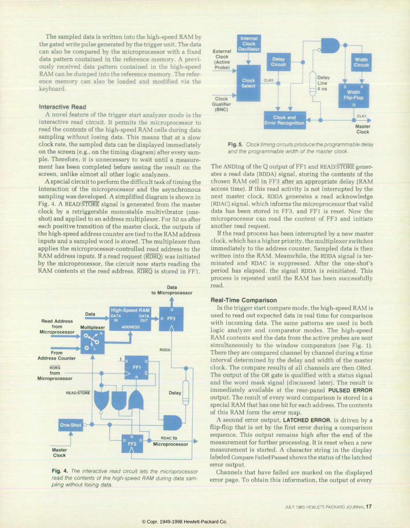
programmable delay and the programmable width of the master clock. A simplified diagram is shown in Fig. 5. The active clock CLKO is a combination of the external or inter nal clock and the clock qualifier input.
The internal clock is generated by a 100-MHz oscillator, divided down in 1-2-5 steps. CLKO triggers the delay circuit, which sets the width flip-flop, which is reset by the width circuit. The flip-flop output is the master clock, CLKi.
Delay and width generation is done mainly with custom ICs, as it is in the 8180A Data Generator (see Fig. 6). How ever, in the analyzer, it is of great importance to keep the
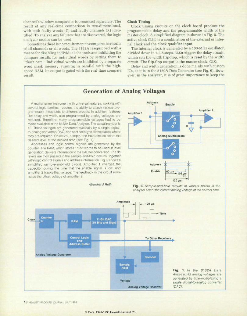
Generation of Analog Voltages
A mult ichannel Instrument with universal features, working with severa l log ic fami l ies , requ i res the ab i l i ty to a t tach var ious pro grammable thresho lds to d i f fe rent probes. In add i t ion, features l i ke de lay and wid th , a lso programmed by ana log vo l tages, are r e q u i r e d . T h e r e f o r e , m a n y p r o g r a m m a b l e v o l t a g e s h a d t o b e m a d e i s i n t h e 8 1 8 2 A D a t a A n a l y z e r . T h e a c t u a l n u m b e r i s 42. These vo l tages are generated cyc l ica l ly by a s ing le d ig i ta l - to-analog converter (DAC) and sent serially to all the places where they the required. On arr ival , sample-and-hold circui ts select the desi red level at the desi red t ime (see Fig. 1) .
A d d r e s s e s a n d l o g i c c o n t r o l s i g n a l s a r e g e n e r a t e d b y t h e counter. The RAM, which stores 1 1-bi t words to be used in level generation, delivers information to the DAC for conversion. The dc levels are then passed to the sample-and-hold c i rcui ts , together w i th a con t ro l s igna ls and address in fo rmat ion . F ig . 2 shows a s i m p l i f i e d s a m p l e - a n d - h o l d c i r c u i t . A m p l i f i e r 1 c h a r g e s t h e c a p a c i t o r d u r i n g t h e t i m e t h a t t h e e n a b l e s i g n a l i s l o w , a n d ampl i f ier 2 t racks that vo l tage. The feedback in the c i rcu i t e l imi nates the of fset vol tage of ampl i f ier 2.
-Bernhard Roth
Address Enable
Amplifier 1 Amplifier 2
120 /
F i g . 2 . S a m p l e - a n d - h o l d c i r c u i t s a t v a r i o u s p o i n t s i n t h e analyzer select the correct analog voltage at the correct t ime.
Amplitude
Clock
-120
- Time
Control Logic and
Address Buffer
Analog Vol tage Generator
To Other Receivers .
Sample/ Hold
Voltage
Analog Voltage Receiver
F i g . 1 . I n t h e 8 1 8 2 A D a t a Ana lyzer , 42 ana log vo l tages are generated by t ime-mul t ip lex ing a s ing le d ig i ta l - to-analog conver ter (DAC).
1 8 H E W L E T T - P A C K A R D J O U R N A L J U L Y 1 9 8 3
© Copr. 1949-1998 Hewlett-Packard Co.
High-Speed Delay
Generator
CLKO
. 0 -5 .9 ns
High-Speed Delay
Generator
6-21.9 ns , \ To Next Stage
Fig. 6. Custom ICs are used in the delay c i rcui t (shown) and the simi lar width circui t . Special high-speed delay generators minimize the delay through the c i rcui t .
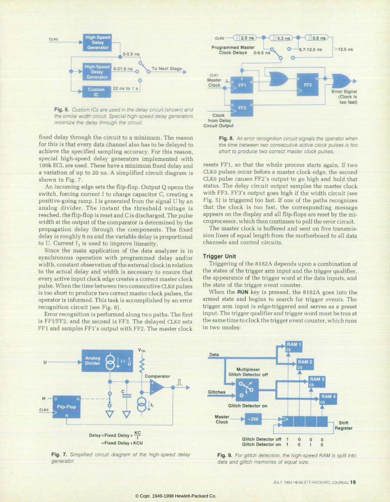
fixed delay through the circuit to a minimum. The reason for this is that every data channel also has to be delayed to achieve the specified sampling accuracy. For this reason, special high-speed delay generators implemented with 100k ECL are used. These have a minimum fixed delay and a variation of up to 20 ns. A simplified circuit diagram is shown in Fig. 7.
An incoming edge sets the flip-flop. Output Q opens the switch, forcing current I to charge capacitor C, creating a positive-going ramp. I is generated from the signal U by an analog divider. The instant the threshold voltage is reached, the flip-flop is reset and C is discharged. The pulse width at the output of the comparator is determined by the propagation delay through the components. The fixed delay is roughly 6 ns and the variable delay is proportional to U. Current ll is used to improve linearity.
Since the main application of the data analyzer is in synchronous operation with programmed delay and/or width, constant observation of the external clock in relation to the actual delay and width is necessary to ensure that every active input clock edge creates a correct master clock pulse. When the time between two consecutive CLKO pulses is too short to produce two correct master clock pulses, the operator is informed. This task is accomplished by an error recognition circuit (see Fig. 8).
Error recognition is performed along two paths. The first is FF1/FF2, and the second is FF3. The delayed CLKO sets FFl and samples FFl's output with FF2. The master clock
> 1 2 . 5 n s P r o g r a m m e d M a s t e r , C l o c k D e l a y s 0 - 6 . 6 n s
Error Signal (Clock Is too fast)
Clock from Delay
Circuit Output
Fig. 8. An error recogni t ion c i rcui t s ignals the operator when the t ime between two consecut ive act ive c lock pulses is too shor t to produce two correct master c lock pu lses.
resets FFl, so that the whole process starts again. If two CLKO pulses occur before a master clock edge, the second CLKO pulse causes FF2's output to go high and hold that status. The delay circuit output samples the master clock with FF3. FFS's output goes high if the width circuit (see Fig. 5) is triggered too fast. If one of the paths recognizes that the clock is too fast, the corresponding message appears on the display and all flip-flops are reset by the mi croprocessor, which then continues to poll the error circuit.
The master clock is buffered and sent on five transmis sion lines of equal length from the motherboard to all data channels and control circuits.
Trigger Unit Triggering of the 8182A depends upon a combination of
the states of the trigger arm input and the trigger qualifier, the appearance of the trigger word at the data inputs, and the state of the trigger event counter.
When the RUN key is pressed, the 8182A goes into the armed state and begins to search for trigger events. The trigger arm input is edge-triggered and serves as a preset input. The trigger qualifier and trigger word must be true at the same time to clock the trigger event counter, which runs in two modes:
D e ! a y = F i x e d D e l a y + ^ =F ixed De lay+KCU
F ig . 7 . S imp l i f i ed c i r cu i t d i ag ram o f t he h i gh -speed de lay generator.
Data
Multiplexer Glitch Detector off
Master Clock Shift
Register
G l i t ch De tec tor o f f 1 G l i t c h D e t e c t o r o n 1
Fig. 9. For g l i tch detect ion, the h igh-speed RAM is spl i t in to data and g l i tch memor ies of equal s ize.
JULY 1983 HEWLETT-PACKARD JOURNAL 19
© Copr. 1949-1998 Hewlett-Packard Co.
1. "Allow gaps yes." After the programmed number of true trigger events has been counted, the trigger event counter activates the trigger delay counter.
2. "Allow gaps no." Only true trigger events that occur one after the other at every master clock time are counted . If a false trigger event is recognized, the counter is reset to zero.
When all trigger conditions are true, the trigger delay counter, which consists of a count-down circuit that can be preset to any value between 0 and 65535, is started. When the delay counter has reached zero, the 8182A responds to the trigger condition. In the trigger start analyzer mode, it begins to write the incoming data into the high-speed RAM. In the In stop analyzer mode, it stops data recording. In the trigger start compare mode, it begins the comparison of incoming data.
All trigger conditions can be set to "don't care," that is, they appear to be always true. The 8182A then starts im mediately with the first incoming active clock edge. The instrument can also be started immediately by pressing the SAMPLE key, which overrides all trigger conditions and generates one clock pulse. Pressing the SAMPLE key re peatedly or holding it down generates additional clock pulses for storing or comparing data manually.
Glitch Detectors Each channel of the 8182A has its own glitch detector. In
contrast to the latch mode found in many analyzers, the glitch detector allows the 8 182 A to differentiate between a data transition and a glitch, which is defined as more than one data transition per sampling interval. To store the de tected glitches in addition to the sampled data, the high-
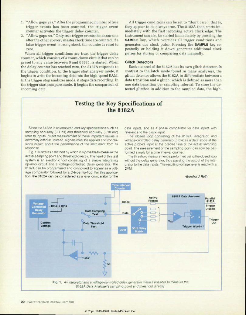
Testing the Key Specifications of the 8182A
Since the 81 82A is an analyzer, and key specif icat ions such as sampl ing accuracy (±1 ns) and threshold accuracy (±10 mV) refer is inputs, d i rect measurement of these impor tant va lues is ext remely d i f f icu l t . Ins tead, s igna ls must be appl ied and conc lu s ions d rawn abou t t he pe r fo rmance o f t he i ns t rumen t f rom i t s response.
Fig. the illustrates a method by which it is possible to measure the ac tua l t es t po in t and th resho ld d i rec t l y . The hea r t o f t h i s t es t sys tem i s an e lec t ron ic too l cons is t i ng o f a s imp le in teg ra t ing op -amp c i r cu i t and a vo l t age -con t ro l l ed de lay gene ra to r . The 8182A can be p rogrammed and con f igu red to appear as a vo l t age compara to r fo l lowed by a D- type f l ip - f lop . For th is app l i ca t ion, the 81 82A can be considered as a level comparator for the
d a t a i n p u t s , a n d a s a p h a s e c o m p a r a t o r f o r d a t a i n p u t s w i t h reference to the c lock input.
T h e c l o s e d l o o p c o n s i s t i n g o f t h e 8 1 8 2 A , i n t e g r a t o r , a n d vo l tage-contro l led delay generator prov ides a data s lope at the ac t ive probe 's input a t the prec ise t ime o f the ac tua l sampl ing po in t . The measurement o f the sampl ing po in t can now be per formed s imply by a t ime in terval counter .
The threshold measurement is performed using the closed loop wi thout the delay generator , thus pass ing the output o f the in te grator to the data inputs. The result ing voltage level is read with a DVM.
-Bernhard Roth
Time Interval Counter
81 82A Data Analyzer
Voltage- Control led
Delay Generator
Control Voltage
Trigger Out
Fig. make . measure the and a voltage-controlled delay generator make it possible to measure the 81 82 A Data Analyzer 's sampl ing point and threshold d i rect ly .
2 0 H E W L E T T - P A C K A R D J O U R N A L J U L Y 1 9 8 3
© Copr. 1949-1998 Hewlett-Packard Co.
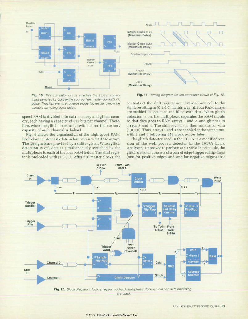
F ig . 10 . Th is co r re la to r c i r cu i t a t taches the t r i gger con t ro l input sampled by CLKO to the appropriate master clock (CLK1) pulse. Thus i t prevents erroneous tr iggering result ing from the var iab le sampl ing point delay.
speed RAM is divided into data memory and glitch mem ory, each having a capacity of 512 bits per channel. There fore, when the glitch detector is switched on, the memory capacity of each channel is halved.
Fig. 9 shows the organization of the high-speed RAM. Each channel stores its data in four 256 x 1-bit RAM arrays. The CS signals are provided by a shift register. When glitch detection is off, data is simultaneously switched by the multiplexer to each of the four RAM fields. The shift regis ter is preloaded with (1,0,0,0). After 256 master clocks, the
To Twin 8182A
C L K O
Master Clock CLKI (Minimum Delay)
Master Clock CLKI (Maximum Delay)
Control Input ci
CICLKO -
C I C L K I (Minimum Delay)
CICLK1 (Maximum Delay)
Fig. 11. T iming d iagram for the corre la tor c i rcu i t o f F ig . 10.
contents of the shift register are advanced one cell to the right, resulting in (0,1,0,0). In this way, all four RAM arrays are enabled in sequence and filled with data. When glitch detection is on, the multiplexer separates the RAM inputs so that data goes to RAM arrays 1 and 2, and glitches to arrays 3 and 4. The shift register is then preloaded with (1,0,1,0). Thus, arrays 1 and 3 are enabled at the same time, with 2 and 4 following 256 clock pulses later.
The glitch detector used in the 8 182 A is a modified ver sion of the well proven detector in the 1615A Logic Analyzer,1 improved to perform at 50 MHz. In principle, the glitch detector consists of a pair of edge- triggered flip-flops (one for positive edges and one for negative edges) that
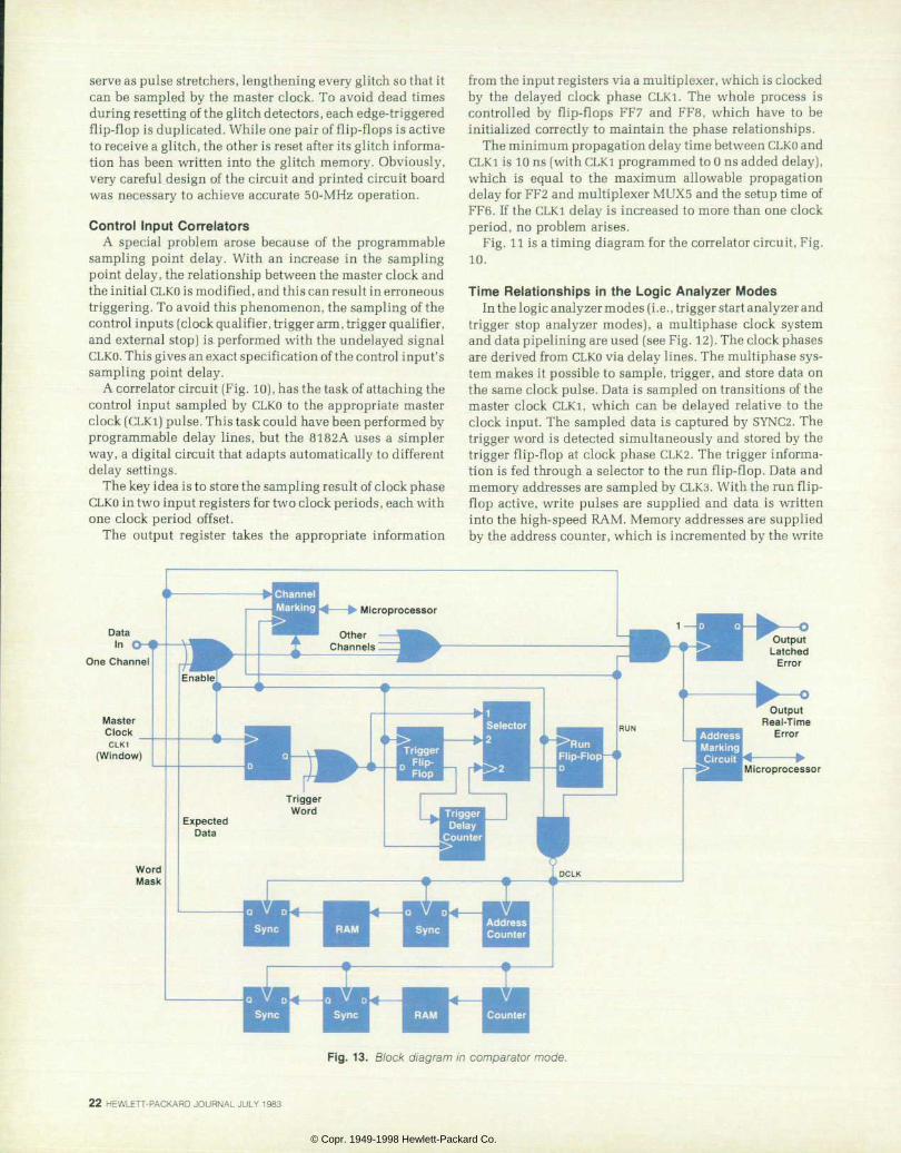
Fig. clock Block diagram in logic analyzer modes. A mult iphase clock system and data pipel ining are used.
JULY 1983 HEWLETT-PACKARD JOURNAL 21
© Copr. 1949-1998 Hewlett-Packard Co.
serve as pulse stretchers, lengthening every glitch so that it can be sampled by the master clock. To avoid dead times during resetting of the glitch detectors, each edge-triggered flip-flop is duplicated. While one pair of flip-flops is active to receive a glitch, the other is reset after its glitch informa tion has been written into the glitch memory. Obviously, very careful design of the circuit and printed circuit board was necessary to achieve accurate 50-MHz operation.
Control Input Correlators A special problem arose because of the programmable
sampling point delay. With an increase in the sampling point delay, the relationship between the master clock and the initial CLKO is modified, and this can result in erroneous triggering. To avoid this phenomenon, the sampling of the control inputs (clock qualifier, trigger arm, trigger qualifier, and external stop) is performed with the undelayed signal CLKO. This gives an exact specification of the control input's sampling point delay.
A correlator circuit (Fig. 10) , has the task of attaching the control input sampled by CLKO to the appropriate master clock (CLKl) pulse. This task could have been performed by programmable delay lines, but the 8182A uses a simpler way, a digital circuit that adapts automatically to different delay settings.
The key idea is to store the sampling result of clock phase CLKO in two input registers f or two clock periods, each with one clock period offset.
The output register takes the appropriate information
from the input registers via a multiplexer, which is clocked by the delayed clock phase CLKl. The whole process is controlled by flip-flops FF7 and FF8, which have to be initialized correctly to maintain the phase relationships.
The minimum propagation delay time between CLKO and CLKl is 10 ns (with CLKl programmed to 0 ns added delay), which is equal to the maximum allowable propagation delay for FF2 and multiplexer MUX5 and the setup time of FF6. If the CLKl delay is increased to more than one clock period, no problem arises.
Fig. 11 is a timing diagram for the correlator circuit, Fig. 10.
Time Relat ionships in the Logic Analyzer Modes In the logic analyzer modes (i.e. , trigger start analyzer and
trigger stop analyzer modes), a multiphase clock system and data pipelining are used (see Fig. 12). The clock phases are derived from CLKO via delay lines. The multiphase sys tem makes it possible to sample, trigger, and store data on the same clock pulse. Data is sampled on transitions of the master clock CLKl, which can be delayed relative to the clock input. The sampled data is captured by SYNC2. The trigger word is detected simultaneously and stored by the trigger flip-flop at clock phase CLK2. The trigger informa tion is fed through a selector to the run flip-flop. Data and memory addresses are sampled by CLK3. With the run flip- flop active, write pulses are supplied and data is written into the high-speed RAM. Memory addresses are supplied by the address counter, which is incremented by the write
One Channel
Microprocessor
Fig . 13 . B lock d iagram in compara to r mode.
2 2 H E W L E T T - P A C K A R D J O U R N A L J U L Y 1 9 8 3
© Copr. 1949-1998 Hewlett-Packard Co.
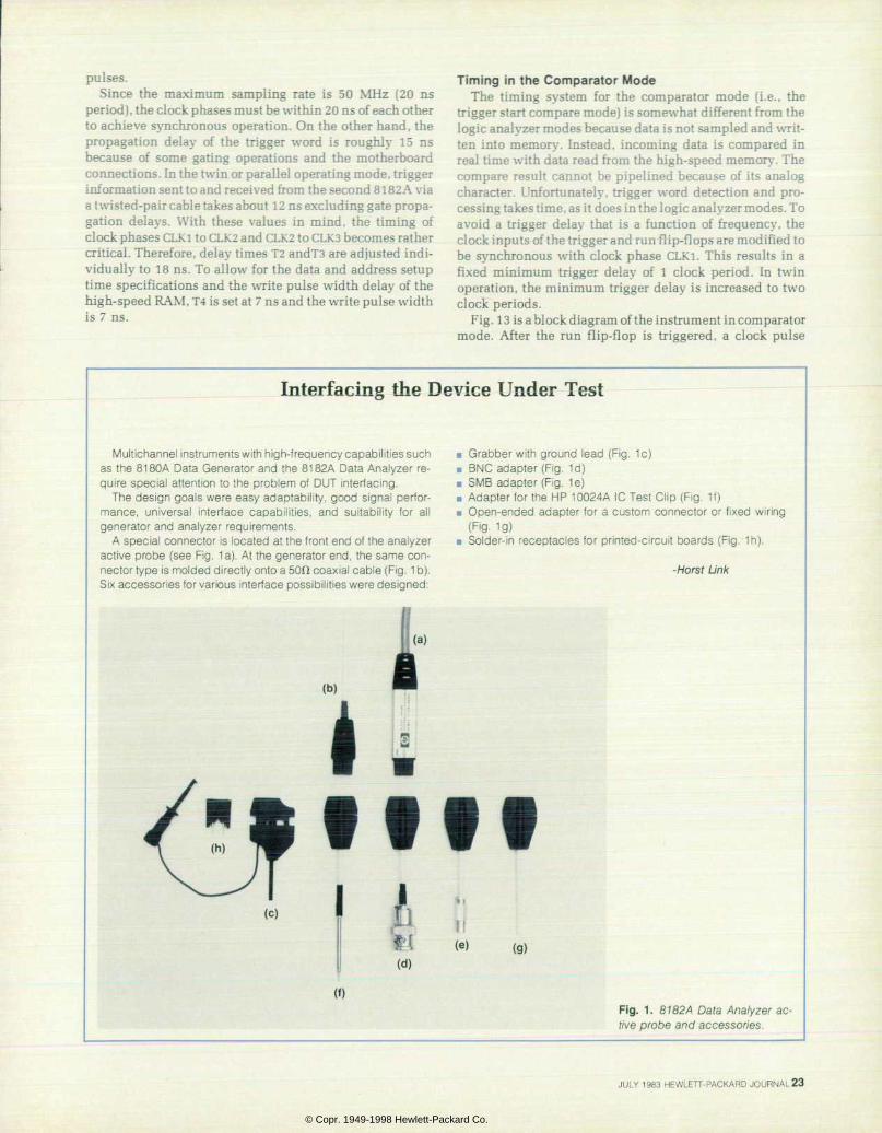
pulses. Since the maximum sampling rate is 50 MHz (20 ns
period) . the clock phases must be within 20 ns of each other to achieve synchronous operation. On the other hand, the propagation delay of the trigger word is roughly 15 ns because of some gating operations and the motherboard connections. In the twin or parallel operating mode, trigger information sent to and received from the second 8182A via a twisted-pair cable takes about 12 ns excluding gate propa gation delays. With these values in mind, the timing of clock phases CLKl to CLK2 and CLK2 to CLK3 becomes rather critical. Therefore, delay times T2 andT3 are adjusted indi vidually to 18 ns. To allow for the data and address setup time specifications and the write pulse width delay of the high-speed RAM, T4 is set at 7 ns and the write pulse width is 7 ns.
Timing in the Comparator Mode The timing system for the comparator mode (i.e., the
trigger start compare mode) is somewhat different from the logic analyzer modes because data is not sampled and writ ten into memory. Instead, incoming data is compared in real time with data read from the high-speed memory. The compare result cannot be pipelined because of its analog character. Unfortunately, trigger word detection and pro cessing takes time, as it does in the logic analyzer modes. To avoid a trigger delay that is a function of frequency, the clock inputs of the trigger and ran flip-flops are modified to be synchronous with clock phase CLKl. This results in a fixed minimum trigger delay of 1 clock period. In twin operation, the minimum trigger delay is increased to two clock periods.
Fig . 1 3 is a block diagram of the instrument in comparator mode. After the run flip-flop is triggered, a clock pulse
Interfacing the Device Under Test
Mult ichannel instruments with high-frequency capabil i t ies such as the 8180A Data Genera to r and the 8182A Data Ana lyzer re qui re specia l at tent ion to the problem of DUT inter fac ing.
The des ign goa ls were easy adaptab i l i t y , good s igna l per fo r m a n c e , a l l i n t e r f a c e c a p a b i l i t i e s , a n d s u i t a b i l i t y f o r a l l generator and analyzer requirements.
A special connector is located at the f ront end of the analyzer ac t ive probe (see F ig . la ) . A t the genera tor end, the same con nector type is molded directly onto a 50ÃÃ coaxial cable (Fig. 1 b). Six accessories for various interface possibi l i t ies were designed:
Grabber w i th ground lead (F ig . 1c) BNC adapter (F ig . 1d) SMB adapter (F ig. 1e) Adapter for the HP 10024A 1C Test Cl ip (F ig. 1f ) Open-ended adapte r fo r a cus tom connec to r o r f i xed w i r ing (Fig. 1g) Solder- in receptacles for pr inted-c i rcui t boards (Fig. 1h).
-Horst Link
¡ t i f f
I]
li (e) (9)
F i g . 1 . 8 1 8 2 A D a t a A n a l y z e r a c t ive probe and accessor ies.
JULY 1983 HEWLETT-PACKARD JOURNAL 23
© Copr. 1949-1998 Hewlett-Packard Co.
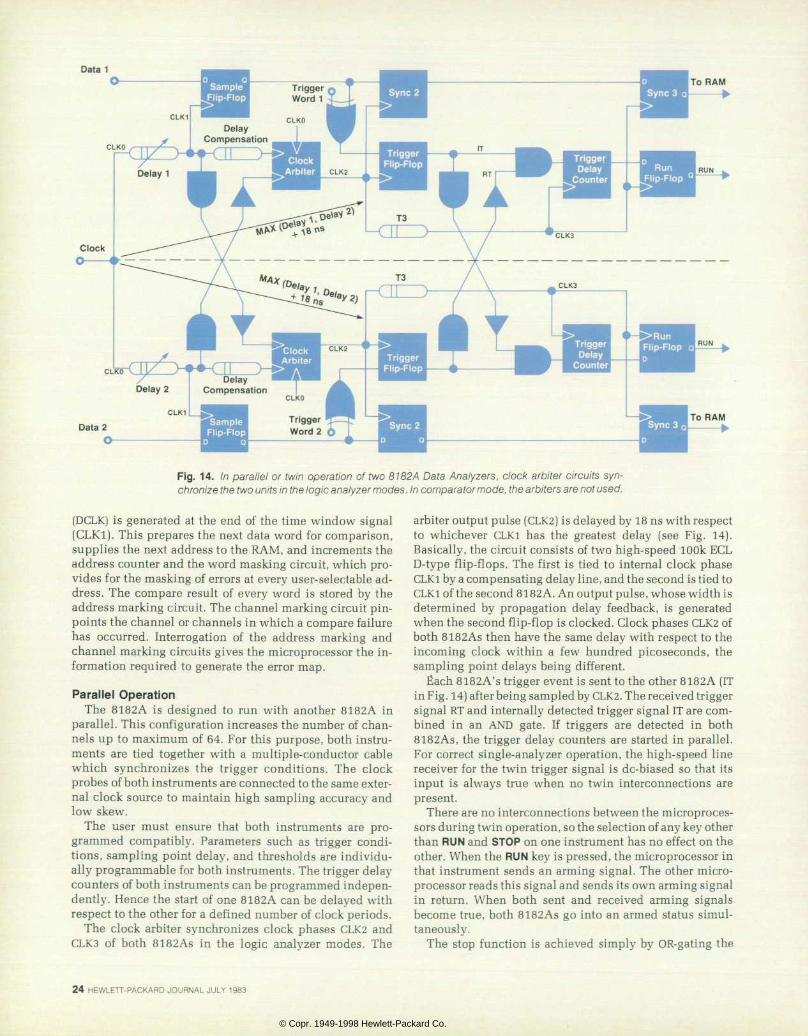
Data 1
Fig . 14 . In para l le l o r tw in opera t ion o f two 8182A Data Ana lyzers , c lock arb i te r c i rcu i ts syn chronize the two units in the logic analyzer modes. In comparator mode, the arbiters are not used.
(DCLK) is generated at the end of the time window signal (CLK1). This prepares the next data word for comparison, supplies the next address to the RAM, and increments the address counter and the word masking circuit, which pro vides for the masking of errors at every user-selectable ad dress. The compare result of every word is stored by the address marking circuit. The channel marking circuit pin points the channel or channels in which a compare failure has occurred. Interrogation of the address marking and channel marking circuits gives the microprocessor the in formation required to generate the error map.
Paral lel Operation The 8182A is designed to run with another 8182A in
parallel. This configuration increases the number of chan nels up to maximum of 64. For this purpose, both instru ments are tied together with a multiple-conductor cable which synchronizes the trigger conditions. The clock probes of both instruments are connected to the same exter nal clock source to maintain high sampling accuracy and low skew.
The user must ensure that both instruments are pro grammed compatibly. Parameters such as trigger condi tions, sampling point delay, and thresholds are individu ally programmable for both instruments. The trigger delay counters of both instruments can be programmed indepen dently. Hence the start of one 8182A can be delayed with respect to the other for a defined number of clock periods.
The clock arbiter synchronizes clock phases CLK2 and CLK3 of both 8182As in the logic analyzer modes. The
arbiter output pulse (CLK2) is delayed by 18 ns with respect to whichever CLKi has the greatest delay (see Fig. 14). Basically, the circuit consists of two high-speed 100k ECL D-type flip-flops. The first is tied to internal clock phase CLKl by a compensating delay line, and the second is tied to CLKI of the second 8182A. An output pulse, whose width is determined by propagation delay feedback, is generated when the second flip-flop is clocked. Clock phases CLK2 of both 8182As then have the same delay with respect to the incoming clock within a few hundred picoseconds, the sampling point delays being different.
Each 8182A's trigger event is sent to the other 8182A (IT in Fig. 14) after being sampled by CLK2. The received trigger signal RT and internally detected trigger signal IT are com bined in an AND gate. If triggers are detected in both 8182As, the trigger delay counters are started in parallel. For correct single-analyzer operation, the high-speed line receiver for the twin trigger signal is de-biased so that its input is always true when no twin interconnections are present.
There are no interconnections between the microproces sors during twin operation, so the selection of any key other than RUN and STOP on one instrument has no effect on the other. When the RUN key is pressed, the microprocessor in that instrument sends an arming signal. The other micro processor reads this signal and sends its own arming signal in return. When both sent and received arming signals become true, both 8182As go into an armed status simul taneously.
The stop function is achieved simply by OR-gating the
2 4 H E W L E T T - P A C K A R D J O U R N A L J U L Y 1 9 8 3
© Copr. 1949-1998 Hewlett-Packard Co.
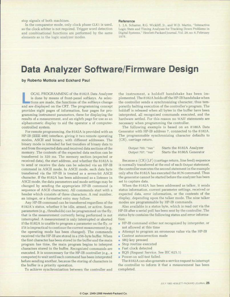
stop signals of both machines. In the comparator mode, only clock phase CLKi is used,
so the clock arbiter is not required. Trigger word detection and combinational functions are performed by the same elements as in the logic analyzer modes.
Reference 1. J.A. Scharrer, R.G. Wickliff, Jr.. and W.D. Martin, "Interactive Logic State and Timing Analyses for Tracking Down Problems in Digital Systems." Hewlett-Packard Journal, Vol. 29. no. 6, February 1978.
Data Analyzer Software/Firmware Design by Roberto Motto la and Eckhard Paul
LOCAL PROGRAMMING of the 8 182 A Data Analyzer is done by means of front-panel softkeys. As selec tions are made, the functions of the softkeys change
and are displayed on the CRT. The programming concept provides eight pages of information, four pages for pro gramming instrument parameters, three for displaying the results of a measurement, and an eighth page for use as an alphanumeric display to aid the operator a of computer- controlled system.
For remote programming, the 8182A is provided with an HP-IB (IEEE 488) interface, giving it two remote operating modes, ASCII and binary, with different addresses. The binary mode is intended for fast transfers of binary data to and from the expected data and received data sections of the memory. The contents of the expected data section can be transferred in 320 ms. The memory section (expected or received data), the start address, and whether the 8182A is to send or receive the data can be selected via an HP-IB command in ASCII mode. In ASCII mode, each data byte transferred via the HP-IB is treated as a seven-bit ASCII character. If the 8182A has been addressed as a listener in ASCII mode, the data parameters and mode settings may be changed by sending the appropriate HP-IB command (a sequence of ASCII characters). All commands start with a header which consists of three characters. A real number, an integer, or a formatted entry may follow.
Any HP-IB command can be transferred regardless of the 8182A's status, whether it be idle, armed, or active. Some parameters (e.g., thresholds) can be programmed on the fly, that is the measurement currently being performed is not interrupted. A measurement is only interrupted or aborted if the 8182A is unable to program a parameter on the fly, or if it is impractical to continue the current measurement (e.g , the operating mode has been changed). The commands received via the HP-IB are stored in a 256-byte buffer. When the first character has been stored in the buffer and the main program has time, the main program begins to interpret characters stored in the buffer. Recognized commands are executed. It is unnecessary for the HP-IB controller (e.g., a computer) to wait until each command has been interpreted before sending another, because the storing of characters in the buffer is a priority operation.
To achieve synchronization between the controller and
the instrument , a holdoff handshake has been im plemented. The 8182A holds off the HP-IB handshake when the controller sends a synchronizing character, thus tem porarily halting execution of the controller's program. The holdoff is released when all bytes in the buffer have been interpreted, all recognized commands executed, and the hardware settled. For this reason no WAIT statements are necessary when programming the controller.
The following example is based on an 8180A Data Generator with HP-IB address 7, connected to the 8182A. The programmable synchronizing character defaults to (CR), carriage return.
Output 703; "run" Output 707; "run"
Starts the 8182A Analyzer Starts the 8180A Generator
Because a (CR)(LF) (carriage return, line feed) sequence is normally transferred at the end of each Output statement, the controller executes the second statement in the example only after the 8182A has executed the RUN command. Thus the generator cannot be started before the analyzer has been set to capture data.
When the 8182A has been addressed as talker, it sends status information, current parameter settings, received or expected data, error information, or the contents of the display, depending upon the talker mode. The nine talker modes are programmable by HP-IB commands.
Also available is a status byte, which is read out via the HP-IB after a serial poll has been sent by the controller. The status byte contains the following status and error informa tion: • HP-IB command either not recognized by interpreter, or
not allowed at this time • Attempt to program an erroneous value via the HP-IB • Context autoconnection made • SRQ key pressed • Stop routine executed • Fast clock detected • RQS (Request Service. See IEC 625.1) • Power-on self-test failed.
The 8182A can also generate a service request to interrupt the controller to inform it that a measurement has been completed.
JULY 1983 HEWLETT-PACKARD JOURNAL 25
© Copr. 1949-1998 Hewlett-Packard Co.
Interrupt
Not Expected Event
Fig. 1. operat ing 8182A Data Analyzer main program resembles a real- t ime mult i task operat ing system. CPU. skil led task dispatcher makes ful l use of the interrupt structure of the CPU.
Program Architecture The structure of the program controlling the 8182A is
designed to obtain good performance from the 8-bit micro processor under varying load conditions. The goal was to guarantee no loss of commands and a prompt response, even in extreme situations. For example, the 8182A might be continuously displaying new data from a repetitive mea surement with the operator varying some parameter using a vernier key, while simultaneously logging the whole pro cess on a computer using the HP-IB local talker capability.
The program is designed around a skilled task dis patcher, which makes full use of the interrupt structure of the 6809 CPU. The resulting structure closely resembles the nucleus of a simple real-time multitask operating system. As illustrated in Fig. 1, five tasks are performed by the dispatcher. It uses a mixture of fixed priority and first come, first served queue structures to select from competing tasks.
Priorities are dynamically variable, that is, the program has the ability to decide when a task is becoming gradually more important and requires extra attention, or when a task can be delayed to conserve CPU resources. This feature allows it to adapt to a wide range of controller speeds and different operating conditions (perhaps a lot of display ac tivity, or a CPU-intensive measurement).
The dispatcher also has the ability to recognize when the operator or controller are sending commands that would cause multiple repetitions of the same action. This situation is flagged when recognized, and the action is executed only once at the last possible moment.
The primary function of the interrupt structure is to inter face the dispatcher to the outside world. This is made pos sible via the keystroke and HP-IB acceptor routines. The respective routines react to the asynchronous stimuli from local or remote commands sent to the processor. A routine checks the commands, then communicates with the dis patcher, which is responsible for further processing. The synchronization of different processes is assured by control
signals between the acceptors and the dispatcher, data being exchanged between them in global areas.
The NMI line of the 6809 is connected to a 10-ms-period time base which triggers the TIMERS module. This module generates eight programmable delay timers and consumes roughly 5% of the total CPU time. The dispatcher uses the delay timers to perform time-related actions that have to be independent of the CPU load, and to supply timing infor mation to the dynamic priority algorithm.
Keystroke Operation The keystroke handler and keystroke processor routines
together manipulate all the commands entered into the 8 182 A via the front-panel keypad (local commands). In the event of no local activity, a simple circuit monitors the keypad. If any key is pressed, an FIRQ interrupt, which calls up the acceptor routine, is generated. The acceptor is re sponsible for keyboard scanning and debouncing the mechanical switches. If a key operation is recognized as valid, the message is placed in a first in, first out (FIFO) buffer, and the dispatcher is told to activate the keystroke processor. The acceptor routine is then complete.
The eight-key FIFO buffer, combined with the interrupt operation, ensures that key action is never lost, even in the case of a heavy CPU load. When the processor takes more time to complete its task the user may perceive a small delay between giving a command and getting a response. The keystroke data is taken from the FIFO buffer by the proces sor. Different processes are selected and triggered from here depending on the program status and the key function. Typical actions are control of the softkey menus, program ming the hardware, and activating the measurement con troller.
By using the TIMERS module, the keystroke processor is also able to reschedule itself periodically when keys calling for an automatic repeat function are selected.
2 6 H E W L E T T - P A C K A R D J O U R N A L J U L Y 1 9 8 3
© Copr. 1949-1998 Hewlett-Packard Co.
HP-IB Operation The HP-IB functions are realized with the acceptor and
processor routines shown in Fig. 1. The acceptor interrupt routine handles all HP-IB activities, but does not interpret ASCII characters received or execute HP-IB commands. Changes of state or address (local, remote, listener, talker) are recognized and stored in RAM. Characters received are stored in a 256-byte buffer in ASCII mode, or in the desired memory location in binary mode. Upon an interrupt, the acceptor disables itself after a state change or if the receiver buffer is full.
The processor executes the state changes, interprets characters stored in the buffer, executes recognized HP-IB commands, and enables the acceptor when the state changes have been executed, or the receiver buffer is no longer full.
The acceptor-processor structure is designed to handle HP-IB activities very quickly. The acceptor stores charac ters without interpreting or executing them. A slow control ler can send the characters on an interrupt-controlled basis. The processor interprets the characters stored in the buffer interactively.
Measurement Control ler The measurement controller is responsible for all pro
cessing related to measurement cycles. The most important activity is the programming of hardware for a RUN, and reading back information generated in the hardware after a STOP.
During measurements, the controller can read informa tion from the hardware as soon as it is generated. This information is also passed to the display updating routines, giving the impression of a real-time instrument.
The controller recognizes when the instrument stops in dependently of external commands. It also generates the synchronization necessary for twin operation, propagating the run and stop commands to the second 8182A. Using the timers, the measurement controller schedules itself in the case of automatically repeated measurement cycles (au- toarming).
Periodic Tasks Two categories of periodic tasks are recognized by the
dispatcher. The first is scheduled every 100 ms. Its primary use is for display activities such as pulsing the clock sym bol, flashing warnings, updating counters and so on. The period of 100 ms is sufficient to assure good message visi bility during a one-shot function.
The second category includes CPU-intensive tasks hav ing a low priority. These are scheduled every 2.5 seconds to keep the demand for CPU time down to 5% of the total. In this category is a routine that checks the rear- panel settings, allowing reaction to an HP-IB address change or a single- twin change without the necessity of a power-off power-on sequence.
A routine for building a CRC (cyclic redundancy check) signature on the 250 bytes of RAM containing the parameter settings is also called every 2.5 seconds. This routine makes it possible to use a CRC algorithm that gives excellent data protection, but is so complex that it would take too much time to compute the CRC after every data change.
D i s p l a y U p d a t i n g The display updating routines are responsible for writing
information to the CRT. Static display changes caused by operator commands and dynamic changes occurring when the instrument is measuring and displaying the incoming results in real tune require two different routine categories.
Self-Test When the 8 182 A is powered up, it executes six self-test
routines. Any error encountered during these routines is displayed as an error message. Tests performed are: 1. RAM/stack test 2. ROM test 3. Keyboard test 4. Clock test 5. Address counter test 6. Data board test.
If tests 1 or 2 fail, the self-test procedure stops because the tested 3 is vital to the remaining tests. If any of tests 3 to 6 fail, the power-up sequence is stopped after completion of the self-test. The program flow resumes after a stop if the user presses the Continue softkey.
The RAM/stack test performs a read/write check of the RAM stack area, then calculates the 16-bit CRC signature of the remaining RAM, storing it repeatedly throughout the stack area. Possible influences between the stack area and the remaining RAM area are checked by building the signa ture for the remaining RAM area again and comparing it with the signatures stored in the stack area.
The ROM test calculates the signature for each ROM, compares the value with the corresponding signature in the self-test ROM, and displays the numbers of any ROMs in which the comparison failed.
The keyboard test causes an error message to be displayed if one or more keys are being pressed, or appear to be pressed (indicating a short circuit), during this routine.
The clock test checks all paths a signal may take through the timing circuits as a result of delay and width parameter settings. Errors are recognized in the clock error circuit.
The address counter test simulates clock pulses and reads the state of the address counter at several times to check that pulses have been counted correctly and ensure that every address bit is able to toggle.
The data board test checks the high-speed RAMs and ascertains the number of data boards installed in the in strument.
It is possible to execute further self-test routines by press ing an unlabeled softkey and entering a password via the keyboard. The tests have been implemented for service and diagnostic purposes.
In addition to the self-tests described above, the HP-IB commands MEW (memory write) and JSR (jump subroutine) provide another powerful test facility. With the MEW com mand, any data can be written into a sequence of RAM addresses. If the data represents 6809 program code, the program can be started via the HP-IB command JSR. In this way, additional test programs can be loaded and executed from a controller via the HP-IB for servicing purposes.
Ini t ial izat ion and Unexpected Events The initialization block of the 81 82 A firmware checks the
JULY 1983 HEWLETT-PACKARD JOURNAL 27
© Copr. 1949-1998 Hewlett-Packard Co.
data stored in the battery-backed RAM for integrity, when selecting between a cold or warm start. It then transfers control to the dispatcher. The unexpected event routine permanently monitors the program flow and some critical data areas to avoid the possibility of a system crash caused by program bugs or a defective RAM.
Developing the F i rmware The 8182A control firmware is based on the microcom
puter board equipped with a 6809 CPU. The 64K address space consists of 44K of ROM (only 40K is actually used), 14K of RAM for parameter and data storage, 4K of display RAM, and 2K of memory-mapped I/O space.
The 6809 was found to be the most suitable 8-bit CPU for this application. The powerful command set includes com plete stack-relative addressing. The local data space of all procedures is in the stack, giving total separation of code and data as well as reentrant and recursive coding.
The 40K-byte program is written entirely in assembly language to extract maximum power from the small CPU and keep the amount of code to a minimum. Most of the procedures are written as structured code and use standard interfaces to communicate with each other. Some excep tions are made in critical areas. Well known synchronizing methods and data exchanging techniques ( f lags , semaphores, mailbox, etc.) are used in the multitask area of the program.
Most of the procedures dealing with programming or the displaying of categories of similar information are written as interpreters, working on information tables. The struc ture of these tables is complex in some cases. For example, the parameter updating procedure derives from its table the command to call itself, and builds a new parameter set in a recursive manner. Another typical example of a table- driven interpreter is the procedure dealing with the softkey menu tree.
Power Supplies for the Stimulus/Response System by Ulr ich Ot to and Horst L ink
IN DESIGNING POWER SUPPLIES for the 8 180 A Data Generator, 8181A Extender, and 8182A Data Analyzer, the most important objectives were high load current
capability and serviceability within a restricted space. The sizes of the instrument cabinets were limited by the
desire to produce a system suitable for benchtop operation. To accommodate the generator, the analyzer, and perhaps two extenders on a bench, the cabinet dimensions obvi ously had to be limited.
The card rack in the generator holds eleven printed cir cuit boards with a spacing of 20 mm between boards. The analyzer has thirteen boards with 17-mm spacing. Because both cabinets also accommodate a CRT display, the space available for power supplies is severely restricted. The outer dimensions for the power supplies were fixed at 254 x 152 x 139 mm.
The high load currents are required especially by the -5.2V rails. In the 8180A Data Generator, the current taken from the —5.2V supply by the Rate ICs alone is approxi mately 7.1 amperes. The total current demanded of the -5.2V supply is on the order of 18.5 amperes. Furthermore, the numerous output amplifier circuits each demand 5.5W from their +15V and -7.5V supplies. In the 8182A Data Analyzer, the complex ECL logic circuits have a total re quirement of some 28 amperes on the -5.2V rail, making this supply the most heavily loaded in the system.
To aid production and serviceability, the decision was
made at an early stage to produce modular supplies consist ing of plug-in units and boards, and to make the three supplies as similar as possible, if not identical.
It soon became evident that the demands made on the 8182A power supply were unusually heavy, and although the concept of switched-mode-with-flyback was adopted for all three instruments' supplies, fundamental differences exist in the 81 82 A supply.
Fig. 1 illustrates all of the main functional blocks of the 8180A supply. After rectification (or doubling and rectifica tion, in the case of a 115V ac input), the value of the poten tial at the switching transistor collector is between 200 and 360V, depending on the line voltage.
Starting Circuit Fig. 2 shows the schematic diagram of the starting circuit
block shown in Fig. 1. A 1000-/uF capacitor is charged via the resistive divider until the potential across it reaches 26V. At this point, Z24 becomes conductive and switches on the drive circuit for the transistor switch. Energy is then fed to the control circuit. When the potential across the capacitor has decayed to 12 V, the transistor switch is turned off and the circuit is ready to begin a new cycle. If no fault condition is sensed by the control circuit, the power supply begins operation before the end of the first start cycle. If, on the other hand, a fault is detected, the start cycle is repeated at three-second intervals. After the start cycle, all primary
2 8 H E W L E T T - P A C K A R D J O U R N A L J U L Y 1 9 8 3
© Copr. 1949-1998 Hewlett-Packard Co.
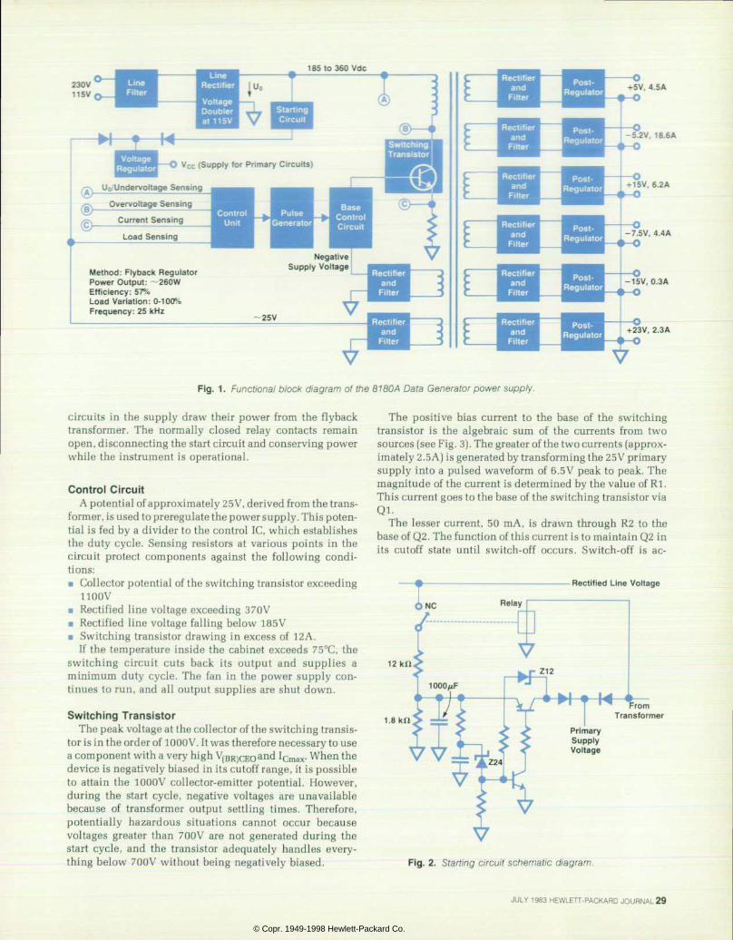
185 to 360 Vdc
Vcc (Supply for Primary Circuits)
Uo/Undervoltage Sensing
Overvortage Sensing
Current Sensing
Negative Supply Voltage Method: Flyback Regulator
P o w e r O u t p u t : - 2 6 0 W Efficiency: 57% Load Variat ion: 0-100% Frequency: 25 kHz
Rectifier and
Filter
Rectifier and
Filter
Rectifier and
Filter
Rectifier and
Filter
Rectifier and
Filter
Post- Regulator
Post- Regulator
Post- Regulator
Post- Regulator
Post- Regulator
+5V, 4 .5A
- 5 . 2 V . 1 8 . 6 A
+ 1 5 V , 6 . 2 A
- 7 . 5 V , 4 . 4 A
- 1 5 V , 0 . 3 A
+ 2 3 V , 2 . 3 A
Fig . power supp ly . b lock d iagram of the 8180A Data Generator power supp ly .
circuits in the supply draw their power from the flyback transformer. The normally closed relay contacts remain open, disconnecting the start circuit and conserving power while the instrument is operational.
Control Circuit A potential of approximately 25V, derived from the trans
former, is used to preregulate the power supply. This poten tial is fed by a divider to the control 1C, which establishes the duty cycle. Sensing resistors at various points in the circuit protect components against the following condi tions: • Collector potential of the switching transistor exceeding
1100V • Rectified line voltage exceeding 370V • Rectified line voltage falling below 185V • Switching transistor drawing in excess of 12A.
If the temperature inside the cabinet exceeds 75°C, the switching circuit cuts back its output and supplies a minimum duty cycle. The fan in the power supply con tinues to run, and all output supplies are shut down.
Switching Transistor The peak voltage at the collector of the switching transis
tor is in the order of 1000V. It was therefore necessary to use a component with a very high V(BR)CEOand Icmax- When the device is negatively biased in its cutoff range, it is possible to attain the 1000V collector-emitter potential. However, during the start cycle, negative voltages are unavailable because of transformer output settling times. Therefore, potentially hazardous situations cannot occur because voltages greater than 700V are not generated during the start cycle, and the transistor adequately handles every thing below 700V without being negatively biased.
The positive bias current to the base of the switching transistor is the algebraic sum of the currents from two sources (see Fig. 3). The greater of the two currents (approx imately 2.5A) is generated by transforming the 25V primary supply into a pulsed waveform of 6.5V peak to peak. The magnitude of the current is determined by the value of Rl. This current goes to the base of the switching transistor via Q l .
The lesser current, 50 mA, is drawn through R2 to the base of Q2. The function of this current is to maintain Q2 in its cutoff state until switch-off occurs. Switch-off is ac-
• Rectified Line Voltage
Relay
1 2 k l l .
M
1 0 0 0 M F
* N T N * Tran
From Transformer
Primary Supply Voltage
Fig . 2 . S tar t ing c i rcu i t schemat ic d iagram.
JULY 1983 HEWLETT-PACKARD JOURNAL 29
© Copr. 1949-1998 Hewlett-Packard Co.
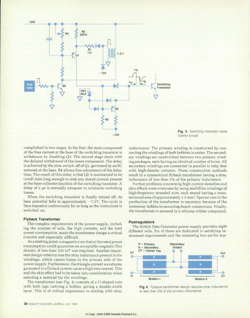
~25V
R 4 ^ 2 2 0 U
< R 1 4 l K - J m 4 H - Â £ 0 1 1 1:3.7
-15V +IB
VR1 Z6.8
V n
-M- -M-
•R3
-^ Switching KJ, Transistor
r \
*
- 1 5 V Fig . 3 . Swi tch ing t rans is to r base control circuit.
complished in two stages. In the first, the main component of the bias current at the base of the switching transistor is withdrawn by disabling Q3. The second stage deals with the delayed withdrawal of the lesser component. The delay is achieved by the slow switch-off of Ql , governed by an RC network at the base. R4 allows fine adjustment of the delay time. The result of this delay is that Q2 is maintained in its cutoff state long enough to sink any stored current present at the base-collector junction of the switching transistor. A delay of 2 /JLS is normally adequate to minimize switching losses.
When the switching transistor is finally turned off, its base potential falls to approximately -7.5V. The cycle is then repeated continuously for as long as the instrument is switched on.
Flyback Transformer The complex requirements of the power supply, includ
ing the number of rails, the high currents, and the total power consumption, made the transformer design a critical concern and especially difficult.
As a starting point, a magnetic core that at the rated power consumption could guarantee an acceptable magnetic flux density of less than 220 mT was required. Another impor tant design criterion was the stray inductance present in the windings, which causes losses in the primary side of the power supply. Furthermore, the triangle current waveforms generated in a flyback system cause a high rms current. This and the skin effect had to be taken into consideration when selecting a material for the windings.
The transformer (see Fig. 4) consists of a U-shaped core with both legs carrying a bobbin, giving a double-width layer. This is of critical importance in dealing with stray
inductances. The primary winding is constructed by con necting the windings of both bobbins in series. The second ary windings are sandwiched between two primary wind ing packages, each having an identical number of turns. All secondary windings are connected in parallel to help deal with high-density currents. These construction methods result in a symmetrical flyback transformer having a stray inductance of less than 3% of the primary inductance.
Further problems concerning high current densities and skin effects were overcome by using multifilar windings of high-frequency stranded wire, each strand having a cross- sectional area of approximately 1.5 mm2. Special care in the production of the transformer is necessary because of the numerous bobbin-to-mounting-board connections. Finally, the transformer is encased in a silicone rubber compound.
Postregulators The 8180A Data Generator power supply provides eight
different rails. Six of these are dedicated to satisfying in strument requirements and the remaining two are for sup-
P = P r i m a r y S = S e c o n d a r y C T = C e n t e r T a p
S e c o n d a r y O u t p u t
Q Out
Bobb in I Bobb in I I
Fig. 4. F lyback t ransformer design reduces st ray inductance to less than 3% of the pr imary inductance.
3 0 H E W L E T T - P A C K A R D J O U R N A L J U L Y 1 9 8 3
© Copr. 1949-1998 Hewlett-Packard Co.
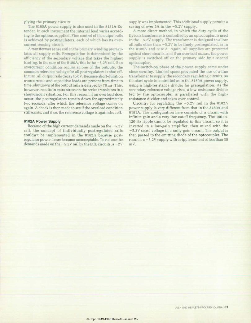
plying the priman- circuits. The 8180A power supply is also used in the 8181A Ex
tender. In each instrument the internal load varies accord ing to the options supplied. Fine control of the output rails is achieved by postregulators. each of which has its over- current sensing circuit.
A transformer sense coil in the primary winding preregu- lates all supply rails. Preregulation is determined by the efficiency of the secondary voltage that takes the highest loading. In the case of the 8180A, this is the —5. 2V rail. If an overcurrent condition occurs at one of the outputs, the common reference voltage for all postregulators is shut off. In turn, all output rails decay to 0V. Because short-duration overcurrents and capacitive loads are present from time to time, shutdown of the output rails is delayed by 70 ms . This , however, results in extra stress on the series transistors in a short-circuit situation. For this reason, if an overload does occur, the postregulators remain down for approximately two seconds, after which the reference voltage comes on again. A check is then made to see if the overload condition still exists, and if so, the reference voltage is again shut off.
8182A Power Supply Because of the high current demands made on the -5.2V
rail, the concept of individually postregulated rails couldn't be implemented in the 8182A because post- regulator power losses became unacceptable. To reduce the demands made on the - 5. 2V rail by the ECL circuits, a -2V
supply was implemented. This additional supply permits a saving of over 5A in the -5.2Y supply.
A more direct method, in which the duty cycle of the flyback transformer is controlled by an optocoupler, is used in the —5.2V supply. The transformer is designed to allow all rails other than -5.2V to be finely postregulated, as in the 8180A and 8181A. Again, all supplies are protected against short circuits, and if an overload occurs, the power supply is switched off on the primary side by a second optocoupler.
The switch-on phase of the power supply came under close scrutiny. Limited space prevented the use of a line transformer to supply the secondary regulating circuits, so the start cycle is controlled as in the 8180A power supply, using a high-resistance divider for preregulation. As the secondary reference voltage rises, a low-resistance divider fed by the optocoupler is paralleled with the high- resistance divider and takes over control.
Circuitry for regulating the -5.2V rail in the 8182A power supply is very different from that in the 8 180 A and 8181A. The configuration here consists of a circuit with infinite gain and a very low cutoff frequency. The 100-to- 120-Hz ripple cannot be regulated in this circuit, so it is inverted in a low-gain amplifier, then mixed with the —5.2V sense voltage in a unity-gain circuit. The output is then passed to the emitting diode of the optocoupler. The result is a —5.2V supply with a ripple content of less than 30 mV.
JULY 1983 HEWLETT-PACKARD JOURNAL 31
© Copr. 1949-1998 Hewlett-Packard Co.
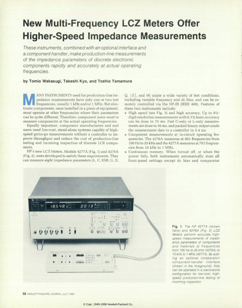
New Multi-Frequency LCZ Meters Offer Higher-Speed Impedance Measurements These instruments, combined with an optional interface and a component handler, make product ion- l ine measurements o f the impedance parameters o f d iscre te e lec t ron ic components rap id ly and accura te ly a t ac tua l opera t ing frequencies.
by Tomio Wakasugi , Takesh i Kyo , and Tosh io Tamamura
MANY INSTRUMENTS used for production-line im pedance measurements have only one or two test frequencies, usually 1 kHz and/or 1 MHz. But elec
tronic components, once installed in a piece of equipment, must operate at other frequencies where their parameters can be quite different. Therefore, component users want to measure components at the actual operating frequencies.
Equally important, component manufacturers and end users need low-cost, stand-alone systems capable of high speed go/no-go measurements without a controller to im prove throughput and reduce the cost of production-line testing and incoming inspection of discrete LCR compo nents.
HP's new LCZ Meters, Models 4277 A (Fig. 1) and 4276A (Fig. 2), were developed to satisfy these requirements. They can measure eight impedance parameters (L, C, ESR, G, D,
Q, | Z | , and 9) under a wide variety of test conditions, including variable frequency and dc bias, and can be re motely controlled via the HP-IB (IEEE 488). Features of these two instruments include: • High speed (see Fig. 3) and high accuracy. Up to 4Vz-
digit-resolution measurements with 0.1% basic accuracy can be done in 70 ms. Fast C-only or L-only measure ments are done in 30 ms, and packed binary output sends the measurement data to a controller in 3.4 ms.
• Component measurements at in-circuit operating fre quencies. The 4276A measures at 801 frequencies from 100 Hz to 20 kHz and the 4277A measures at 701 frequen cies from 10 kHz to 1 MHz.
• Continuous memory. When turned off, or when the power fails, both instruments automatically store all front-panel settings except dc bias and comparator
F i g . 1 . T h e H P 4 2 7 7 A ( s h o w n h e r e ) a n d 4 2 7 6 A ( F i g . 2 ) L C Z M e t e r s p e r f o r m a c c u r a t e h i g h s p e e d m e a s u r e m e n t s o f i m p e d ance pa rame te rs o f componen ts a n d m a t e r i a l s a t f r e q u e n c i e s from 100 Hz to 20 kHz (4276 A) or 10 kHz to 1 MHz (4277 A). By add i n g a n o p t i o n a l c o m p a r a t o r / c o m p o n e n t - h a n d l e r i n t e r f a c e ( s h o w n i n t h e f o r e g r o u n d ) , t h e y can be operated in a s tand-a lone c o n f i g u r a t i o n f o r l o w - c o s t , h i g h speed p roduc t i on - l i ne t es t i ng o r incoming inspect ion.
3 2 H E W L E T T - P A C K A R D J O U R N A L J U L Y 1 9 8 3
© Copr. 1949-1998 Hewlett-Packard Co.
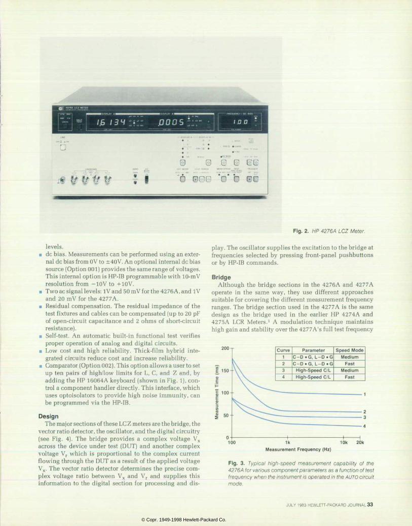
D â € ¢ .
0 0 G G
F ig . 2 . HP 4276A LCZ Mete r .
levels. • de bias. Measurements can be performed using an exter
nal dc bias from 0V to ±40V. An optional internal dc bias source (Option 001) provides the same range of voltages. This internal option is HP-IB programmable with 10-mV resolution from -10V to +10V.
• Two ac signal levels: IV and 50 mV for the 4276A, and IV and 20 mV for the 4277 A.
• Residual compensation. The residual impedance of the test fixtures and cables can be compensated (up to 20 pF of open-circuit capacitance and 2 ohms of short-circuit resistance).
• Self-test. An automatic built-in functional test verifies proper operation of analog and digital circuits.
• Low cost and high reliability. Thick-film hybrid inte grated circuits reduce cost and increase reliability.
• Comparator (Option 002). This option allows a user to set up ten pairs of high/low limits for L, C, and Z and, by adding the HP 16064A keyboard (shown in Fig. 1), con trol a component handler directly. This interface, which uses optoisolators to provide high noise immunity, can be programmed via the HP-IB.
Design The major sections of these LC Z meters are the bridge, the
vector ratio detector, the oscillator, and the digital circuitry (see Fig. 4). The bridge provides a complex voltage Vx across the device under test (DUT) and another complex voltage Vr which is proportional to the complex current flowing through the DUT as a result of the applied voltage Vx. The vector ratio detector determines the precise com plex voltage ratio between Vx and Vr and supplies this information to the digital section for processing and dis
play. The oscillator supplies the excitation to the bridge at frequencies selected by pressing front-panel pushbuttons or by HP- IB commands.
Bridge Although the bridge sections in the 4276A and 4277A
operate in the same way, they use different approaches suitable for covering the different measurement frequency ranges. The bridge section used in the 4277A is the same design as the bridge used in the earlier HP 4274A and 4275A LCR Meters.1 A modulation technique maintains high gain and stability over the 4277A's full test frequency
200 -r
100 1k Measurement Frequency (Hz)
— I 1 1 0 k 2 0 k
F i g . 3 . T y p i c a l h i g h - s p e e d m e a s u r e m e n t c a p a b i l i t y o f t h e 4276 A for various component parameters as a function of test frequency when the instrument is operated in the AUTO circuit mode.
JULY 1983 HEWLETT-PACKARD JOURNAL 33
© Copr. 1949-1998 Hewlett-Packard Co.
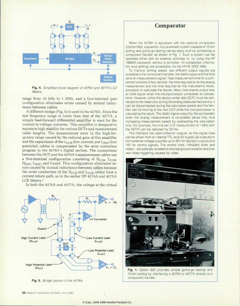
Digital Section
F ig . 4 . S imp l i f i ed b lock d iag ram o f 4276A and 4277 A LCZ Meters.
range from 10 kHz to 1 MHz, and a four-terminal pair configuration eliminates errors caused by mutual induc tance between cables.
A different design {Fig. 5} is used in the 4276A. Since the test frequency range is lower than that of the 4277A, a simple feed-forward differential amplifier is used for the current- to- vol tag e converter. This amplifier is designed to maintain high stability for various DUTs and measurement cable lengths. The measurement error in the high-fre quency range caused by the reduced gain of this amplifier and the capacitance of the LCUR (low current) and LPOT (low potential) cables is compensated by the error correction program in the 4276A's digital section. The connections between the DUT and the 4276A's measurement cables use a five-terminal configuration consisting of HCUR, LCUR, HPOT, LPOT, and Guard. This configuration eliminates er rors caused by mutual inductance between cables because the outer conductors of the HCUR and LCUR cables form a current return path, as in the earlier HP 4274A and 4275A LCR Meters.1
In both the 4276A and 4277A, the voltage at the virtual
V, = -¡Rr
High Current Lead (HCUR)
High Potential Lead (HPOT)
Fig . 5 . Br idge sec t ion o f the 4276A.
= ¡2,
Comparator
W h e n t h e 4 2 7 6 A i s e q u i p p e d w i t h t h e o p t i o n a l c o m p a r a t o r (Option 002), a powerful, fully automatic system capable of 1 0-bin sort ing and go/no-go test ing can be easi ly bui l t by connect ing a componen t hand le r as shown in F ig . 1 . Such a sys tem can be opera ted e i ther w i th an ex terna l cont ro l le r o r , by us ing the HP 16064A keyboard , w i thout a cont ro l le r . A l l compar ison in forma t ion and set t ings are accessib le v ia the HP-IB ( IEEE 488).
To Imp rove so r t i ng speed , two d i f f e ren t ou tpu t s i gna l s a re available to the component handler, the INDEX signal and the EOM (end-of-measurement) s ignal . Total measurement t ime for a com ponent consists of two periods: the t ime required to do the analog measurement and the t ime requ i red fo r the ins t rument 's mic ro processor to calculate the resul ts. Many instruments output only an EOM s igna l when the mic roprocessor comple tes i t s ca lcu la t ions. However , s ince the dev ice under tes t (DUT) must be con nected to the meter only during the analog measurement period, it can be d isconnected dur ing the ca lcu la t ion per iod and the han dler can be moving to the next DUT whi le the microprocessor is calculating the result. The INDEX signal output by the comparator when the ana log measu remen t i s comp le ted a l l ows th i s , t hus inc reas ing measurement speed by sub t rac t ing the ca lcu la t ion t ime. For example, the t ime per C-D measurement at 1 MHz with the 4277A can be reduced by 20 ms .
Th is in ter face has open-co l lec tor outputs , so the s ignal l ines can be driven from an internal TTL-level 5V supply (al l outputs) or from external voltage supplies up to 30V for decision outputs and 15V for control signals. The control l ines — TRIGGER, EOM, and INDEX — are optically isolated to provide ground isolation and pre vent fa lse t r igger ing caused by noise.
F i g . 1 . O p t i o n 0 0 2 p r o v i d e s s i m p l e g o / n o - g o t e s t i n g a n d 1 0-bin sort ing by interfacing a 4276 A or 4277 A direct ly to a component hand ler .
34 HEWLETT-PACKARD JOURNAL JULY .1983
© Copr. 1949-1998 Hewlett-Packard Co.
nf
Reference Phase De tec to r
Dua l -S lope A-to-D
C o n v e r t e r
T o Dig i ta l
Sect ion
F ig . 6 . B lock d iag ram o f t he vec t o r r a t i o d e t e c t o r u s e d i n t h e 4276A and 4277 A LCZ Meters.
ground point (LpOT) is zero when the bridges are balanced. Then
Therefore,
V
Therefore, all that is needed to calculate the complex impedance of the DUT is the value of Rr and the vector ratio between Vx and Vr.
The bridge sections in the 4276A and 4277A are fabri cated using custom thick-film hybrid integrated circuits to reduce cost and space.
Vector Rat io Detector Fig. 6 shows a simplified block diagram of the high-speed
Phase Detector 0°
Fig . 7 . Vec tor d iagram showing the or thogona l components o f V x a n d V , a t t h e i n p u t o f t h e p h a s e d e t e c t o r . 8 1 i s t h e reference phase error .
vector ratio detector section used in both LCZ meters. This section detects the precise complex voltage ratio between the two signals Vx and Vr from the bridge section. To obtain good tracking characteristics and linearity for various sig nal levels, the two signals are time-multiplexed by switch Si. The process amplifier block contains attenuators and variable-gain amplifiers to optimize the signal level to the phase detector. The four-phase generator provides the pre cision 90° phase rotations used to detect the orthogonal components of the input signals to the phase detector.
Fig. 7 is a vector diagram showing Vx, Vr, and the x and y coordinates as determined by the reference phase detector. Here a, b, c, and d are the orthogonal components of Vr and Vx detected by the phase detector and defined in the following equation.
V ,
c + jd
a + jb
ac + bd
a2 + b2
ad - be
a2 + b2 = x + j y
The vector ratio detector used in the earlier HP 42 74A and 4275A LCR Meters requires four integration cycles and two dc reference current sources, and measures the four com ponents a, b, c, and d separately by using dual-slope
Fig . 8 . Compar ison o f the dc and ac d ischarge methods fo r determin ing the or thogonal components a, b , c , and d of the vo l tages Vx and Vr
JULY 1983 HEWLETT-PACKARD JOURNAL 35
© Copr. 1949-1998 Hewlett-Packard Co.
Step:
S1 vr
Fig. 9 . Measurement sequence for the vector ra t io detector . The s teps are 1) re ference phase detect ion, 2) autozero, 3) f i r s t f o r conve rs i on f o r a , 4 ) second A - to -D conve rs i on f o r f t , and 5) third A-to-D conversion for y. In the reference phase detect ion step, the output signal Q of the f l ip-f lop (see Fig. 6) goes h igh coinc identa l ly wi th the zero-crossing point of V¡, thus detect ing the reference phase 0°
analog-to-digital conversion (dc discharge method).1 To improve measurement speed, the dual-slope analog-to- digital converter in the 4276A and 4277A measures the scalar ratio between two components directly without any dc reference source (ac discharge method). This increases measurement speed by eliminating one integration cycle and reduces cost by eliminating the dc reference sources. If only the reactive component of impedance is measured, the ac discharge method requires only one integration cycle, further increasing measurement speed. Fig. 8 shows the difference in steps between the two methods.
The vector ratio x + jy is calculated as
ac + bd y + a/3 a2 + b2 1 + a2
a d - b e f t - a y and y =
2 + b2 1 + a2
where a = b/a, /3 = d/a, and y = c/a. Then the unknown impedance Zx is given by
B — ay
1 + a 2 1 + a 2
The measurement sequence of the vector ratio detector consists of five steps which include reference phase detec tion and autozeroing (see Fig . 9) . The reference phase detec tor is used to minimize the reference phase error 0^ (Fig. 7). Since the discharge period of the first integration cycle is proportional to 0a, reducing 6l reduces measurement time.
To minimize Oit reference phase detection in the 4276A uses high-speed clock signals (nf) which are multiples of the test frequencies (see Fig. 6). The 4277A uses the same automatic phase adjust technique used in the 4261A LCR Meter.2
For high-speed inductance or capacitance measure ments, only ft =d/a is detected. Equation (1) implies that when the reference phase error 0a is negligible (i.e., a = b/a is very small), the unknown impedance Zx is approxi mately equal to -Rr(y + j/8). Thus the unknown reactance is simply obtained by dividing or multiplying by the fac tor 27rf.
The phase-detected signal of Fig. 6 has to be converted into a dc voltage very quickly for high-speed measure ments. In the 4277 A, a simple low-pass RC filter is used to reject the ripple component of the phase-detected signal. However, the 4276A's lower frequency range requires a different approach. The low-pass RC filter, which would have too long a settling time at the lower frequencies, is replaced by a preintegrator (Fig . 10) whose integration time is equal to a multiple of the test signal period. Therefore, the output V0 is exactly proportional to the dc component of the input signal. Thus, even at the lowest frequency of 100 Hz,
Dual-Slope A-to-D
Converter
To Digital Section
Fig. detector A preintegrator is used in the 4276A's vector rat io detector to convert the phase- detected s ignal to a dc vol tage precisely proport ional to the dc component of the input s ignal .
3 6 H E W L E T T - P A C K A R D J O U R N A L J U L Y 1 9 8 3
© Copr. 1949-1998 Hewlett-Packard Co.
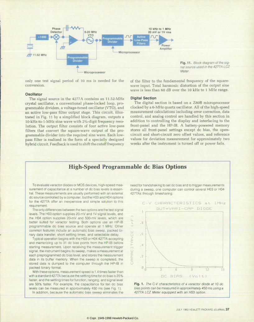
- Microprocessor
only one test signal period of 10 ms is needed for the conversion.
O s c i l l a t o r The signal source in the 427 7 A contains an 11.52-MHz
crystal oscillator, a conventional phase-locked loop, pro grammable dividers, a voltage-tuned oscillator (VTO), and an active low-pass filter output stage. This circuit, illus trated in Fig. 11 by a simplified block diagram, outputs a 10-kHz-to-l-MHz sine wave with 2Vz-digit frequency reso lution. The output filter consists of four active low-pass filters that convert the square-wave output of the pro grammable divider into the required sine wave. Each low- pass filter is realized in the form of a specially designed hybrid circuit. Feedback is used to shift the cutoff frequency
10 kHz to 1 MHz 2 0 m V o r W r m s
Power Amplifier
Fig. 1 1 . Block diagram oà the sig nal source used in the 4277 A LCZ Meter.
of the filter to the fundamental frequency of the square- wave input. Total harmonic distortion of the output sine wave is less than 60 dB over the 10 kHz to 1 MHz range.
D i g i t a l S e c t i o n The digital section is based on a Z80B microprocessor
clocked by a 6-MHz quartz oscillator. All of the high-speed measurement calculations including error correction, data control, and analog control are handled by this section in addition to controlling the display and interfacing to the front-panel and the HP-IB. A battery-powered memory stores all front-panel settings except dc bias, the open- circuit and short-circuit zero offset values, and reference values for deviation measurement for approximately two weeks after the instrument is turned off or power fails.
High-Speed Programmable dc Bias Options
To evaluate varactor d iodes or MOS devices, h igh-speed mea surement of capaci tance at a number of dc b ias levels is essen t ial . These measurements are usual ly performed with an external dc source control led by a computer, but the H03 and H04 options fo r the 4277A o f fe r an inexpens ive and s imp le so lu t ion to th is requirement.
The only differences between the two options are the test signal levels. The H03 option supplies 20-mV and 1 V signal levels, and the H04 op t i on supp l i es 20 -mV and 500-mV leve ls , wh ich a re be t te r su i t ed fo r va rac to r t es t i ng . Bo th op t i ons use an HP- IB p r o g r a m m a b l e d c b i a s s o u r c e a n d o p e r a t e a t 1 M H z . O t h e r common fea tu res inc lude an au tomat i c b ias sweep, packed b i nary data t ransfer , short set t l ing t imes, and selectable delay.
Typical operat ion begins with the H03 or H04 4277A accept ing and memor iz ing up to 31 dc b ias po in ts f rom the HP- IB be fore s tar l ing measurement . Upon receiv ing the measurement t r igger signal, the instrument begins i ts sweep, makes a measurement at each preprogrammed dc bias level , and stores the measurement da ta i n i t s bu f fe r memory . When the sweep i s comp le ted , t he s t o r e d d a t a i s d u m p e d t o t h e c o m p u t e r t h r o u g h t h e H P - I B i n packed binary format.
With these options, measurement speed is 1 .4 times faster than with 25% standard 4277A because the settling time for dc bias is 25% faster, and the settl ing times for function, ranging, and signal level a re 50% fas te r . Fo r examp le , t he capac i tance fo r t en dc b ias leve ls can be measured in approx imate ly 450 ms (see F ig . 1) .
In addi t ion, because the automat ic b ias sweep el iminates the
need for handshaking to set dc bias and to tr igger measurements dur ing a sweep, one computer can cont ro l severa l H03 or H04 4277As through t imeshar ing.
C - V C H R R R C T E R I S T I C S a t 1 M H z
D U T = V H R I - C R P D I O D E
L C
LJ U Z c h H u rx 1 C U
1
. 6
. 4
. 2
3 B
D C B I R S
9 1 2
C Vo 1 t 3
15
Fig . 1 . The C-V character is t ics o f a varactor d iode a t 10 dc bias points can be measured in approximately 450 ms using a 4277 A LCZ Meter equipped wi th an H03 opt ion.
JULY 1983 HEWLETT-PACKARD JOURNAL 37
© Copr. 1949-1998 Hewlett-Packard Co.
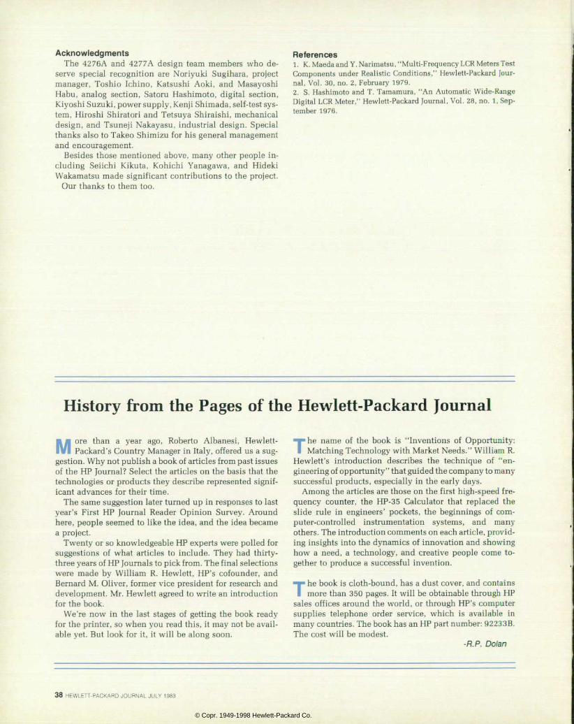
Acknowledgments The 4276A and 4277A design team members who de
serve special recognition are Noriyuki Sugihara, project manager, Toshio Ichino, Katsushi Aoki, and Masayoshi Habu, analog section, Satoru Hashimoto, digital section, Kiyoshi Suzuki, power supply, Kenji Shimada, self-test sys tem, Hiroshi Shiratori and Tetsuya Shiraishi, mechanical design, and Tsuneji Nakayasu, industrial design. Special thanks also to Takeo Shimizu for his general management and encouragement.
Besides those mentioned above, many other people in cluding Seiichi Kikuta, Kohichi Yanagawa, and Hideki Wakamatsu made significant contributions to the project.
Our thanks to them too.
References 1. K. Maeda and Y. Narimatsu, "Multi-Frequency LCR Meters Test Components under Realistic Conditions," Hewlett-Packard Jour nal, Vol. 30, no. 2, February 1979. 2. S. Hashimoto and T. Tamamura, "An Automatic Wide-Range Digital LCR Meter," Hewlett-Packard Journal, Vol. 28, no. 1, Sep tember 1976.
History from the Pages of the Hewlett-Packard Journal
More than a year ago, Roberto Albanesi, Hewlett- Packard's Country Manager in Italy, offered us a sug
gestion. Why not publish a book of articles from past issues of the HP Journal? Select the articles on the basis that the technologies or products they describe represented signif icant advances for their time.
The same suggestion later turned up in responses to last year's First HP Journal Reader Opinion Survey. Around here, people seemed to like the idea, and the idea became a project.
Twenty or so knowledgeable HP experts were polled for suggestions of what articles to include. They had thirty- three years of HP Journals to pick from. The final selections were made by William R. Hewlett, HP's cofounder, and Bernard M. Oliver, former vice president for research and development. Mr. Hewlett agreed to write an introduction for the book.
We're now in the last stages of getting the book ready for the printer, so when you read this, it may not be avail able yet. But look for it, it will be along soon.
The name of the book is "Inventions of Opportunity: Matching Technology with Market Needs." William R.
Hewlett's introduction describes the technique of "en gineering of opportunity" that guided the company to many successful products, especially in the early days.
Among the articles are those on the first high-speed fre quency counter, the HP-35 Calculator that replaced the slide rule in engineers' pockets, the beginnings of com puter-controlled instrumentation systems, and many others. The introduction comments on each article, provid ing insights into the dynamics of innovation and showing how a need, a technology, and creative people come to gether to produce a successful invention.
The book is cloth-bound, has a dust cover, and contains more than 350 pages. It will be obtainable through HP
sales offices around the world, or through HP's computer supplies telephone order service, which is available in many countries. The book has an HP part number: 92233B. The cost will be modest.
-P .P. Do/an
3 8 H E W L E T T - P A C K A R D J O U R N A L J U L Y 1 9 8 3
© Copr. 1949-1998 Hewlett-Packard Co.
Authors July 1983
K l a u s - P e t e r B e h r e n s I Klaus-Peter joined Bòb-
l ingen Instruments Division in 1978 after receiving his engineer ing d ip loma f rom the University of Stuttgart.
| He was responsible for the design of the software and digital control in the 81 80A
l ' f ' I D a t a G e n e r a t o r a n d t h e 8181A Data Generator Extender. Klaus-Peter is marr ied and l ives in Bobl ingen. In h is spare t ime he bui lds model ra i lways.
A n d r e a s W i l b s Andreas Wilbs was born in 1953 in Hei lbronn, West Germany. He jo ined HP in 1980 as a sales support
I engineer for logic s ignal sources, and s ince 1981
: has been a product market ing engineer. He designed
I the special ist t raining pack age for the 81 80A/81A/82A and is responsible for the system's post- int roduct ion act iv i t ies. Andreas is married and enjoys all kinds of outside activities inc lud ing por tab le v ideo record ing.
Werne r Be rke l Werner Berkel was born in Speyer and at tended
i school in Kar lsruhe, where I he received his degree in
1 979. He contributed to the ¡ design of the 8180A and j superv ised the design of
the 15413ATr i -Sta te Uni t I and the 15414A Tr i -State
Pod. Werner enjoys music, soccer, and table ten n is. He is marr ied and l ives in Bobl ingen.
U l r i c h H u b n e r Born and ra ised in Stuttgart, Ulrich Hübner studied at the technical univers i t ies of Aachen and Stuttgart . He joined HP's
m Bobl ingen Medical Division * in 1967, then movedto the
instrument lab, where he deve loped low-cos t osc i l
loscopes. He was responsib le for the hardware design of the 81 70A Logic Pattern Generator, then served as pro jec t manager for the 8180A/8181A Data Generator . Ulr ich is marr ied, has one chi ld, and enjoys swimming and skiing in his spare time.
Jose f Becke r Jo Becker jo ined HP to-
I wards the end of 1979, having previously worked at the University of Stuttgart as a b iomedical engineer . He was responsible for the design of the 81 80A Data
1 Generator output 'É amplifiers, and has now
moved to the fiber optics group at HP's Boblingen Instruments Divis ion, where he is involved in the development of detector heads. Jo is married and has three sons. His hobbies include amateur radio and astronomy.
Heinz Nüssle Heinz Nüssle was born in Boblingen and came to HP as an apprent ice in 1967.
' Af ter h is apprent iceship, j he studied at the University j of Stuttgart , where he
gained h is engineer ing degree in 1 980. In 1 981 he returned to HP and contr ib
u ted to the des ign of the 8180A Data Generator and the development o f the 15413A/15414A Tr i - State Uni t and Pod. Heinz is a member of the German Red Cross and en joys whi te-water kayaking.
U l r i c h S c h o t t m e r Ulrich Schottmer joined HP in 1981, and has con t r i buted to the h igh-speed digi ta l control of the8182A Data Analyzer. He received h is engineer ing degree at the Universi ty of Bochum. Ulr ich l ives in Bobl ingen and enjoys radio-control led aircraft and ski ing.
Mar t in D ie tze Mart in Dietze has been a project engineer wi th HP s ince 1980. He received h is engineer ing degree
' f rom the Universi ty of Stuttgart in 1979. Mart in
1 was involved in the de ve lopment of the 8182A Da ta Ana lyze r and de
signed the high-speed counters and gl i tch detec to rs . Born in Le ipz ig and now a res ident o f Bob l ingen, Mar t in en joys t rave l ing, backpack ing, cy c l ing, and playing the viol incel lo.
D ie te r K ib le Dieter Kible was born near Lake Constance, and graduated f rom the Univer sity of Stuttgart in 1 975. He jo ined HP shor t ly a f ter wards, contr ibut ing to hardware and sof tware des ign o f the 8165A Pro grammable Signal Source.
He has been pro ject leader for the 8182A Data Analyzer s ince 1978. Dieter is a member of DKE. the German counterpar t o f the IEC, work ing on inst rument bus systems. He is marr ied, has two sons, and spends much of his spare time working on h is house and p lay ing tenn is and cards
B e m h a r d R o t h Born and raised near Lake Constance, Bernhard earned h is degree at U lm in 1978. He jo ined HP the
I same year, and began work on the 8182A Data Analyzer. He designed the
. ac t i ve p robe, inpu t i t . ampl i f iers , c lock t iming
c i rcui ts , and log vol tage generator for that instrument. A member of the HP table tennis team, he is s ing le and en joys rock music concer ts and motion pictures.
R o b e r t o M o t t o l a I Tà LLI I I Robert° Motto|a ¡s a nat¡ve
^ M k I o f l t a | y . a n d a t t e n d e d t h e â € ¢ V V V U b U n i v e r s i t y o f T r i e s t e ,
J P w -  » . - * g r a d u a t i n g i n 1 9 7 6 . H e moved to Germany and jo ined HP in 1979, af ter three years of research in digital ¡mage processing. Roberto developed the
operat ing concept for the 8180A/81 A/82A Data Generator and Analyzer system, and par t o f the 81 82A control program. He is married and has two children. He spends his spare time with his family, swimming, l istening to classical music, and bui ld ing a model ra i lway.
Eckha rd Pau l I Eckhard Paul was born
near Flensburg in Northern Germany, and graduated f rom the Fachhochschule of Kiel in 1981. He jo ined HP the same year and has
I been responsible for the HP-IB and self- test soft-
I ware in the8182A Data Ana lyzer . Eckhard is unmarr ied , and en joys p lay ing cards, sk i ing, camping, and cyc l ing.
H o r s t L i n k Horst Link joined HP in 1970, and spent h is ear ly years on the mechanical des ign o f tape punches and readers for calculators and da ta acqu is i t i on sys tems. He la ter became
| responsible for the mechan ica l des ign o f var i
ous pu lse and data generator mainf rames and modules for use in 1-GHz pulse generators and the 8170A Log ic Pat tern Generator . Hors t i s mar ried, has a ten-year old daughter and l ives in Bob l ingen. He spends much of h is f ree t ime work ing around h is house and h ik ing . He is a lso an ac compl ished photographer .
JULY 1983 HEWLETT-PACKARD JOURNAL 39
© Copr. 1949-1998 Hewlett-Packard Co.
Ulrich Otto Ulr ioh Otto jo ined HP in
t 1979. He was responsib le ! forthe design of the power
suppl ies for the 8180A, 1 81 81 A, and 8182A. He I received his BSEE from the I School of Engineer ing in I Essl ingen in 1976, and I went on to gain h is MSEE
at the University of Stuttgart. A native of Stuttgart, U l r ich now l ives in Ehningen, near Bobl ingen. He en joys tennis , swimming, running, and reading, and spends much o f h is spare t ime h ik ing in the mounta ins in summer and downhi l l sk i ing in the winter.
T o s h i o T a m a m u r a à Since joining Yokogawa-
Hewlett-Packard in 1971, Tosh io Tamamura has been a pr inc ipal contr ib-
«* utor to the design of several i HP LCR mete rs . He de
veloped the analog section circuitry for the 4277A LCZ Meter and des igned some
of the hybr id in tegrated c i rcu i ts . He has a BSEE degree received in 1971 f rom the Univers i ty of E lect ro-Communicat ions. He is marr ied and the father of two chi ldren, and l ikes playing tennis.
Tomio Wakasugi After graduat ing wi th a
a BSEE degree f rom Waseda I Universi ty in 1976, Tomio
Wakasugi worked for three years in te lecommun ica t ions before joining Yokogawa-Hewlet t -Pack- ard in 1979. He worked on the 4192A LF impedance
Analyzer and designed the sel f - test systems for the 41 93A Vector Impedance Meter. He designed the ana log sec t ion fo r the 4276A LCZ Meter . Be s ides being captain of VHP's vol leybal l team, h is interests include tennis, jazz, and amateur radio.
Takeshi Kyo Takeshi Kyo jo ined Yokogawa-Hewlet t -Pack- ard in 1970 af ter receiv ing his BEE degree from Iwate Univers i ty . He contr ibuted
! to the design of the4271A 1-MHz LCR Meter and the
[ 4274A and 4275A LCR Meters . He deve loped the
software for the 4276A and 4277A LCZ Meters. He is marr ied, has one daughter , and en joys sk i ing and p lay ing GO, a Japanese game s im i la r to chess.
Address Cor rec t ion Requested Hewle t t -Packard Company, 3000 Hanover
Street, Palo Al to, Cal i fornia 94304
H E W L E T T - P A C K A R D J O U R N A L J U L Y 1 9 8 3 V o l u m e 3 4 . N u m b e r 7
Technical Informat ion f rom the Laborator ies of Hewlet t -Packard Company
Hewlet t -Packard Company. 3000 Hanover St reet Palo Al to. Cal i fornia 94304 U.S.A.
Hewlet t -Packard Centra l Mai l ing Depar tment Van Heuven Goedhar t laan 121
1181 KK Amste lveen. The Nether lands Yokogawa-Hewle t t -Packard L td . . Sug inami -Ku Tokyo 168 Japan
Hewlet t -Packard (Canada) Ltd ' Goreway Dr ive . Miss issauga. Ontar io L4V 1M8 Canada
Bulk Rate U.S. Postage
Paid Hewlett-Packard
Company
0200020707 fc£C PL AC eCAOO M R C A B L A C K E L R N J O H N H O P K I N S U N I V A P P L I E D P H Y S I C S L A B J O H N S H O P K I N S R O L A U R E L M D 2 0 7 0 7
/ " * L J A m a i l i n g s e n d C S e n d p A r \ r \ C D f i O O â € ¢ T o c h a n g e y o u r a d d r e s s o r d e l e t e y o u r n a m e f r o m o u r m a i l i n g l i s t p l e a s e s e n d u s y o u r o l d a d d r e s s l a b e l . S e n d changes to Hewle t t -Packard Journa l , 3000 Hanover S t ree t , Pa lo A l to . Ca l i fo rn ia 94304 U.S.A. A l low 60 days .
5953-8513
© Copr. 1949-1998 Hewlett-Packard Co.