1992-8645 integration and implimentation … · section 2 overview of the fpga and micro blaze. in...
TRANSCRIPT
Journal of Theoretical and Applied Information Technology 10
th June 2015. Vol.76. No.1
© 2005 - 2015 JATIT & LLS. All rights reserved.
ISSN: 1992-8645 www.jatit.org E-ISSN: 1817-3195
127
INTEGRATION AND IMPLIMENTATION SYSTEM-ON-A-
PROGRAMMABLE-CHIP (SOPC) IN FPGA
A.ZEMMOURI1, MOHAMMED ALAREQI
1,3, R.ELGOURI
1,2, M.BENBRAHIM
1,2, L.HLOU
1
1Laboratory of Electrical Engineering and Energy System. Faculty of Sciences, University Ibn Tofail
Kenitra, Morocco.2Laboratory of Engineering Systems, National School of Applied Sciences, University Ibn Tofail Kenitra,
Morocco. 3Community College, Sana'a, Yemen.
E-mail: [email protected],
ABSTRACT
The real-time hardware application is developed around a FPGA hardware architecture that includes embedded
processor MicroBlaze on the field programmable gate array (FPGA).This paper introduces a design of a Micro Blaze
soft-core processor system that can be running the output pins (XGI Expansion Headers Protocol) as such as clock
generator to feed external circuits. The designed processor system is programmed in C language to manage, and
specify the number of clock generators selected. It focuses on implementation XGI Expansion Headers Protocol and an
interface RS232 serial communication on a Xilinx FPGA, which allows bidirectional data transfer with an external
application.
The aim of the paper is twofold. Firstly, to synthesize a processor on Xilinx FPGA chip and then to control of
Expansion Headers inputs / outputs of the board through implementation code compiled in C language on the
MicroBlaze processor. This implementation has been simulated using ISE Simulator (ISim) software tools and the
design to be implemented targeting Virtex5 (XUPV5-LX110T).
Keywords: Processor Microblaze, FPGA, EDK, SDK, RS232, UART, XGI Expansion Headers Protocol.
1. INTRODUCTION
Many digital and transistor logic circuit (such
as processors, microcontrollers, etc.) can develop
System-on-chip (SOC), but what is interesting, is to
design the (SOPC) using the latest programmable
device so as to use the features of FPGA. FPGAs
based Micro Blaze soft-core processor system
controller is the choice of every controller designer,
because of the design fidelity, flexibility, and
simplicity. In recent years, several architectures that combine processors and /or reconfigurable circuit (FPGA) have been proposed to accelerate the execution of applications more complex such as digital signal generator navigation [1]. On the other hand, Introducing MicroBlaze as an Infrastructure for Performance Modeling [2], Processing of Image Data Using FPGA-Based MicroBlaze Core [3] and the system design Micro Blaze ring, which may be housed to act as a system of pulse-width modulation [4]. Reconfigurable architectures represent an appropriate response through offering better performance compared to programmable architectures and more flexibility compared to wired
solutions. It uses reconfigurable logic components that allow the user to modify the architecture in software after fabrication by software part, unlike ASICs whose algorithms are wired into the silicon. The term refers to the reconfiguration operation, is to implement embedded components that present a new functionality without changing the hardware architecture of the system, such as the embedded processor that offers a Micro Blaze, enables control in robotics technology [5]. The Biological doping level of a neural network as the abstraction close to real neurons in the FPGA [6], signal processing and the studies are continuing to control the exchange with a satellite. The MicroBlaze is a virtual microprocessor that is built by combining blocks of code called cores inside a Xilinx Field Programmable Gate Array (FPGA) [7].
EDK helps the designer to construct a processor
system with peripherals on FPGAs .The processor
system can then be programmed to act as what the
designer aims; the soft-core processor used in this
work is MicroBlaze type.
Journal of Theoretical and Applied Information Technology 10
th June 2015. Vol.76. No.1
© 2005 - 2015 JATIT & LLS. All rights reserved.
ISSN: 1992-8645 www.jatit.org E-ISSN: 1817-3195
128
The target of the paper is to design a Micro
Blaze soft-core processor system that can be
running the output pins (XGI Expansion Headers
Protocol) as such as clock generator to feed
external circuits to implement on FPGA, using
EDk.
XGI allows to control of external circuits such
as capture cards, machines, robots, etc.
This paper presents a methodology for
implementation XGI Expansion Headers Protocol
and an interface RS232 serial communication on a
Xilinx FPGA.
The rest of this paper is organized as follows:
Section 2 overview of the FPGA and Micro Blaze.
In Section 3 configuration of
Hardware part for led and dips switch on the board,
Configuration of software part and Addition,
Configuration and Programming two externals
peripherals using dip switch and XGI expansion
headers. Simulation and experimental results in
section 4. Finally, the concluding remarks given in
Section5.
2. OVERVIEW OF THE FPGA AND
MICROBLAZE
FPGA contains programmable logic components called logic blocks and a hierarchy of reconfigurable interconnects that allow the blocks to be "wired together ". Logic blocks can be configured to perform complex combinational functions or merely simple logic gates like “AND” and “XOR”. In most of the FPGA`s, the logic blocks also include memory elements which may be simple flip flops or more complete blocks of memory.
The ML505 board, which was used in this study, includes several input devices, output devices, and data ports, allowing many designs to be implemented without the need for any other components.
Moreover, the configuration and programming of FPGA include follow two basic steps:
First, the configuration of the hardware that focuses on the choice of devices such as a programmed processor, memory, input and associated with the FPGA outputs.
In a second step, programming and implementation of C code in the FPGA board to manage the system.
These operations are to discover new tools from Xilinx EDK includes software (Xilinx Embedded Development Kit) which gives access to both environments: XPS (Xilinx Platform Studio)
responsible in creating purely embedded components and the connections respectful enter them (Hardware side) and SDK (Software Development Kit) responsible in the programming of these components by the C/C++ (software side).
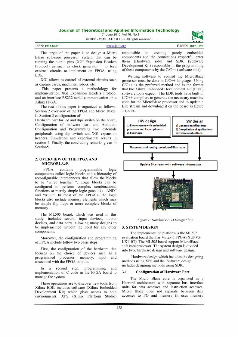
Writing software to control the MicroBlaze processor must be done in C/C++ language. Using C/C++ is the preferred method and is the format that the Xilinx Embedded Development Kit (EDK) software tools expect. The EDK tools have built in C/C++ compilers to generate the necessary machine code for the MicroBlaze processor and to update a Bite stream and download it on the board as figure 1 shows.
Figure 1: Standard FPGA Design Flow.
3. SYSTEM DESIGN
The implementation platform is the ML505 evaluation board that has Virtex-5 FPGA (XUPV5-LX110T). The ML505 board support MicroBlaze soft-core processor. The system design is divided into two; hardware design and software design.
Hardware design which includes the designing methods using XPS and the Software design includes designing methods using SDK.
3.1 Configuration of Hardware Part
The Micro Blaze core is organized as a Harvard architecture with separate bus interface units for data accesses and instruction accesses. Micro Blaze does not separate between data accesses to I/O and memory (it uses memory
Journal of Theoretical and Applied Information Technology 10
th June 2015. Vol.76. No.1
© 2005 - 2015 JATIT & LLS. All rights reserved.
ISSN: 1992-8645 www.jatit.org E-ISSN: 1817-3195
129
mapped I/O). The processor has up to three interfaces for memory accesses: Local Memory Bus (LMB), IBM’s On-chip Peripheral Bus (OPB), and Xilinx CacheLink (XCL). The LMB provides single-cycle access to on-chip dual-port block RAM (BRAM).
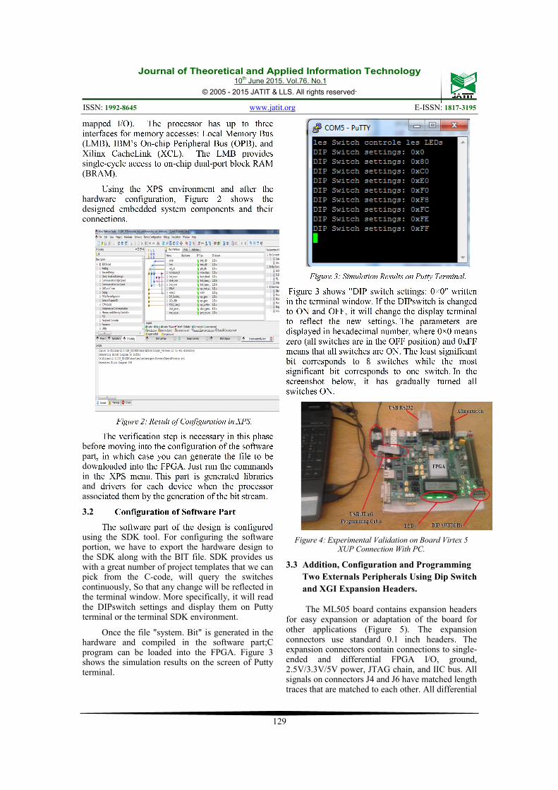
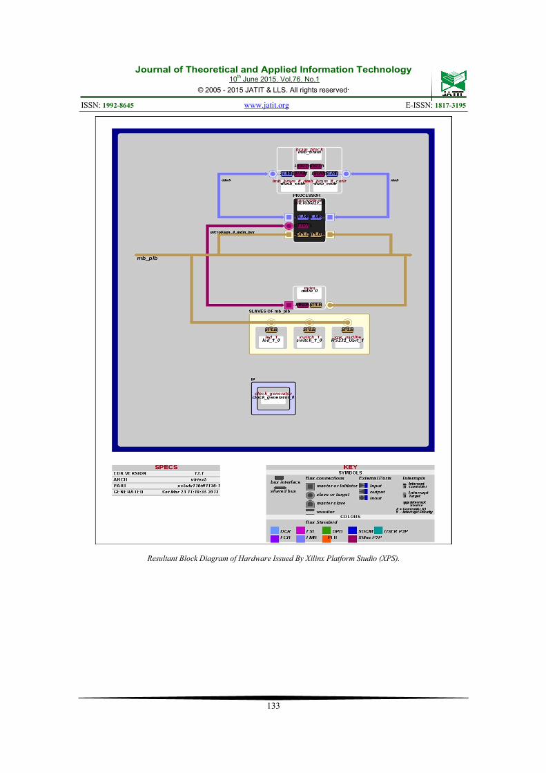
Using the XPS environment and after the hardware configuration, Figure 2 shows the designed embedded system components and their connections.
Figure 2: Result of Configuration in XPS.
The verification step is necessary in this phase before moving into the configuration of the software part, in which case you can generate the file to be downloaded into the FPGA. Just run the commands in the XPS menu. This part is generated libraries and drivers for each device when the processor associated them by the generation of the bit stream.
3.2 Configuration of Software Part
The software part of the design is configured using the SDK tool. For configuring the software portion, we have to export the hardware design to the SDK along with the BIT file. SDK provides us with a great number of project templates that we can pick from the C-code, will query the switches continuously, So that any change will be reflected in the terminal window. More specifically, it will read the DIPswitch settings and display them on Putty terminal or the terminal SDK environment.
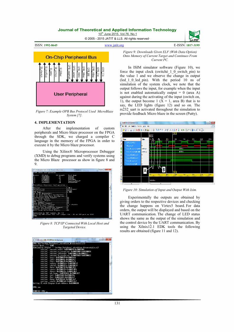
Once the file "system. Bit" is generated in the hardware and compiled in the software part;C program can be loaded into the FPGA. Figure 3 shows the simulation results on the screen of Putty terminal.
Figure 3: Simulation Results on Putty Terminal.
Figure 3 shows "DIP switch settings: 0×0" written in the terminal window. If the DIPswitch is changed to ON and OFF, it will change the display terminal to reflect the new settings. The parameters are displayed in hexadecimal number, where 0×0 means zero (all switches are in the OFF position) and 0xFF means that all switches are ON. The least significant bit corresponds to 8 switches while the most significant bit corresponds to one switch. In the screenshot below, it has gradually turned all switches ON.
Figure 4: Experimental Validation on Board Virtex 5 XUP Connection With PC.
3.3 Addition, Configuration and Programming
Two Externals Peripherals Using Dip Switch
and XGI Expansion Headers.
The ML505 board contains expansion headers for easy expansion or adaptation of the board for other applications (Figure 5). The expansion connectors use standard 0.1 inch headers. The expansion connectors contain connections to single-ended and differential FPGA I/O, ground, 2.5V/3.3V/5V power, JTAG chain, and IIC bus. All signals on connectors J4 and J6 have matched length traces that are matched to each other. All differential

Journal of Theoretical and Applied Information Technology 10
th June 2015. Vol.76. No.1
© 2005 - 2015 JATIT & LLS. All rights reserved.
ISSN: 1992-8645 www.jatit.org E-ISSN: 1817-3195
130
signals are routed with 100Ω differential trace impedance.
Header J6 contains 32 single-ended signal connections to the FPGA I/Os. This permits the signals on this connector to carry high-speed, single-ended data. All single-ended signals on connector J6 are matched length traces. The VCCIO of these signals can be set to 2.5V or 3.3V by setting jumper J20.
Figure 5: Extensions Connectors (XGI) and 8 Dips Switches.
By adding to the hardware configuration uniprocessor, two externals peripherals using the XPS interface "Create or import a new peripheral Wizard" command [8], [9], [10], [11]. The first is the Dip switch 1 will enter a signal of 1byte (On or Off) and the second is the pin N°18 of J6 connector that will provide output signals to an external LED (Figure 6). In our experience, the J20 adjusted at 3.3v.
Figure 6: Blocks Associated With MicroBlaze.
Creating embedded custom peripherals using Xilinx Platform Studio (XPS) is straightforward because XPS automates most of the design creation. The Base System Builder (BSB) wizard reduces the design effort to a series of selections. We can then further customize our design in Project Navigator and XPS. Design customization can be as simple as tweaking a few parameters on existing intellectual
property (IP) cores (for example, changing the baud rate for the AXI UARTLite), or as complex as designing custom IP and integrating it into the existing design.
It creates for each custom peripheral the framework of the design, including bus interface logic, LUTs, registers, and provides an HDL template so that we can integrate our custom logic in an understandable manner.
The tables I and II, show the number of the used logic slice Registers, Slice LUTs and others for led_1_0 peripheral and switch_1_0 peripheral.
Table 1: Post Synthesis Device Utilization of Led_1_0.
Resource Type Used Available Percent
Slice Registers 143 69120 0
Slice LUTs 60 69120 0
LUT Flip Flop pairs
used 157 NA NA
fully used LUT-FF
pairs 46 157 29
unique control sets 14 NA NA
IOs 202 NA NA
bonded IOBs 0 640 0
Table 2: Post Synthesis Device Utilization of Switch_1_0.
Resource Type Used Available Percent
Slice Registers 40 69120 0
Slice LUTs 23 69120 0
LUT Flip Flop
pairs used 53 NA NA
fully used LUT-FF
pairs 10 53 18
unique control sets 9 NA NA
IOs 202 NA NA
bonded IOBs 0 640 0
The communication that takes place between the peripherals and the Micro blaze is OPB. The significance of the top-level module of your custom peripherals must contain a set of bus ports that conforms to OPB or PLB (Processor Local Bus) protocol, so it can be connected to the system or OPB, PLB bus. See figure 7.
Journal of Theoretical and Applied Information Technology 10
th June 2015. Vol.76. No.1
© 2005 - 2015 JATIT & LLS. All rights reserved.
ISSN: 1992-8645 www.jatit.org E-ISSN: 1817-3195
131
Figure 7: Example OPB Bus Protocol Used MicroBlaze System [7].
4. IMPLEMENTATION
After the implementation of custom peripherals and Micro blaze processor on the FPGA through the SDK, we charged a compiler C language in the memory of the FPGA in order to execute it by the Micro blaze processor.
Using the Xilinx® Microprocessor Debugger (XMD) to debug programs and verify systems using the Micro Blaze processor as show in figure 8 and 9.
Figure 8: TCP/IP Connected With Local Host and Targeted Device.
Figure 9: Downloads Given ELF (With Data Option)
Onto Memory of Current Target and Continues From
Current PC.
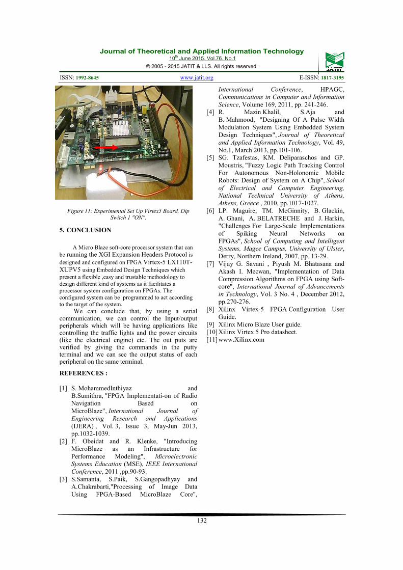
In ISIM simulator software (Figure 10), we force the input clock (switchè_1_0_switch_pin) to the value 1 and we observe the change in output (led_1_0_led_pin). With the period 10 ns of simulation of the system clock, we note that the output follows the input, for example when the input is not enabled automatically output = 0 (area A) against during the activating of the input (switch on, 1), the output become 1 (X = 1, area B) that is to say, the LED lights (figure 12) and so on. The rs232_uart is activated throughout the simulation to provide feedback Micro blaze in the screen (Putty).
Figure 10: Simulation of Input and Output With Isim.
Experimentally the outputs are obtained by giving orders to the respective devices and checking the change happens on Virtex5 board. For data orders, the output will be displayed and based on the UART communication. The change of LED status shows the same as the output of the simulation and the control device by the UART communication. By using the Xilnix12.1 EDK tools the following results are obtained (figure 11 and 12).
Journal of Theoretical and Applied Information Technology 10
th June 2015. Vol.76. No.1
© 2005 - 2015 JATIT & LLS. All rights reserved.
ISSN: 1992-8645 www.jatit.org E-ISSN: 1817-3195
132
Figure 11: Experimental Set Up Virtex5 Board, Dip Switch 1 "ON".
5. CONCLUSION
A Micro Blaze soft-core processor system that can
be running the XGI Expansion Headers Protocol is
designed and configured on FPGA Virtex-5 LX110T-
XUPV5 using Embedded Design Techniques which
present a flexible ,easy and trustable methodology to
design different kind of systems as it facilitates a
processor system configuration on FPGAs. The
configured system can be programmed to act according
to the target of the system. We can conclude that, by using a serial communication, we can control the Input/output peripherals which will be having applications like controlling the traffic lights and the power circuits (like the electrical engine) etc. The out puts are verified by giving the commands in the putty terminal and we can see the output status of each peripheral on the same terminal.
REFERENCES :
[1] S. MohammedInthiyaz and
B.Sumithra, "FPGA Implementati-on of Radio
Navigation Based on
MicroBlaze", International Journal of
Engineering Research and Applications
(IJERA) , Vol. 3, Issue 3, May-Jun 2013,
pp.1032-1039.
[2] F. Obeidat and R. Klenke, "Introducing
MicroBlaze as an Infrastructure for
Performance Modeling", Microelectronic
Systems Education (MSE), IEEE International
Conference, 2011 ,pp.90-93.
[3] S.Samanta, S.Paik, S.Gangopadhyay and
A.Chakrabarti,"Processing of Image Data
Using FPGA-Based MicroBlaze Core",
International Conference, HPAGC,
Communications in Computer and Information
Science, Volume 169, 2011, pp. 241-246.
[4] R. Mazin Khalil, S.Aja and
B. Mahmood, "Designing Of A Pulse Width
Modulation System Using Embedded System
Design Techniques", Journal of Theoretical
and Applied Information Technology, Vol. 49,
No.1, March 2013, pp.101-106.
[5] SG. Tzafestas, KM. Deliparaschos and GP.
Moustris, "Fuzzy Logic Path Tracking Control
For Autonomous Non-Holonomic Mobile
Robots: Design of System on A Chip", School
of Electrical and Computer Engineering,
National Technical University of Athens,
Athens, Greece , 2010, pp.1017-1027.
[6] LP. Maguire, TM. McGinnity, B. Glackin,
A. Ghani, A. BELATRECHE and J. Harkin,
"Challenges For Large-Scale Implementations
of Spiking Neural Networks on
FPGAs", School of Computing and Intelligent
Systems, Magee Campus, University of Ulster,
Derry, Northern Ireland, 2007, pp. 13-29.
[7] Vijay G. Savani , Piyush M. Bhatasana and
Akash I. Mecwan, "Implementation of Data
Compression Algorithms on FPGA using Soft-
core", International Journal of Advancements
in Technology, Vol. 3 No. 4 , December 2012,
pp.270-276.
[8] Xilinx Virtex-5 FPGA Configuration User
Guide.
[9] Xilinx Micro Blaze User guide.
[10] Xilinx Virtex 5 Pro datasheet.
[11] www.Xilinx.com
Journal of Theoretical and Applied Information Technology 10
th June 2015. Vol.76. No.1
© 2005 - 2015 JATIT & LLS. All rights reserved.
ISSN: 1992-8645 www.jatit.org E-ISSN: 1817-3195
133
Resultant Block Diagram of Hardware Issued By Xilinx Platform Studio (XPS).