2 mos direct path flip-flops for process-resilient...
TRANSCRIPT

Research ArticleDPFFs: C2MOS Direct Path Flip-Flops for Process-ResilientUltradynamic Voltage Scaling
Myeong-Eun Hwang1 and Sungoh Kwon2
1Memory Division, Samsung Electronics Inc., Hwaseong, Gyeonggi 18448, Republic of Korea2School of Electrical Engineering, University of Ulsan, Nam-gu, Ulsan 44610, Republic of Korea
Correspondence should be addressed to Sungoh Kwon; [email protected]
Received 10 February 2016; Accepted 3 April 2016
Academic Editor: Ahmed M. Soliman
Copyright © 2016 M.-E. Hwang and S. Kwon. This is an open access article distributed under the Creative Commons AttributionLicense, which permits unrestricted use, distribution, and reproduction in any medium, provided the original work is properlycited.
We propose twomaster-slave flip-flops (FFs) that utilize the clocked CMOS (C2MOS) technique with an internal direct connectionalong the main signal propagation path between the master and slave latches and adopt an adaptive body bias technique to improvecircuit robustness. C2MOS structure improves the setupmargin and robustness while providing full compatibility with the standardcell characterization flow. Further, the direct path shortens the logic depth and thus speeds up signal propagation, which can beoptimized for less power and smaller area.Measurements from test circuits fabricated in 130 nm technology show that the proposedFF operates down to 60mV, consuming 24.7 pW while improving the propagation delay, dynamic power, and leakage by 22%, 9%,and 13%, respectively, compared with conventional FFs at the iso-output-load condition. The proposed FFs are integrated into an8 × 8 FIR filter which successfully operates all the way down to 85mV.
1. Introduction
The rapidly growing volume of data processing and trans-ferring in contemporary clocked electronics has constantlydrawn considerable attention to the design of high speed low-power yet robust sequential timing elements. With a clocknetwork, these sequential components account for 30% to60% of total power consumption in VLSI systems [1]. More-over, the propagation delay and latency of the timing units areresponsible for a large portion of the cycle time as the operat-ing frequency increases. As a result, FF selection and designhave a great effect on both reducing power dissipation andproviding more slack time for easier time-budgeting in high-performance applications.
FFs and latches are the major building blocks of digitalcircuits, and their primary function is to store binary data.Many commercial digital applications selectively use master-slave and pulse-triggered FFs. Examples of the master-slaveflip-flop (MSFF) include the transmission gate-based FF [2],push-pull D-type FF [3], and true single phase clocked FF(TSPC) [4]. Despite popularity of high-performance design,the TSPC can malfunction when the slope of the clock is
insufficiently steep. Slow clocks can cause both the clockedpull-up and pull-down networks to be on simultaneously,resulting in undefined value of the state and race condition.Further, transistor sizing is critical to achieve correct func-tionality in the TSPC. With improper sizing, glitches mayalso occur at the output due to a race condition when theclock transits [5]. Ishikawa et al. proposed a MSFF in whicha hysteresis characteristic of the input circuit of the slavelatch prevents the output whichwas once inverted frombeinginverted again in the metastable state [6]. Another edge-triggered FF is the sense amplifier based FF [7]. All thesehard-edged FFs are characterized by positive setup time,causing a large cycle time. Alternatively, the pulse-based FFs(PBFFs) [8–10] have been widely used to decrease the data-to-output (D-to-Q) delay. In scan logic of the PBFF, however,the scan control becomes too complex and incompatible withthe conventional MSFF for more enhancement of the D-to-Q speed of the FF. The PBFF requires the addition ofpulse generators internally or externally, which can causean increase in area and power and routing congestion, eventhough external pulse generation scheme would provide sev-eral advantages such as shareability among the neighboring
Hindawi Publishing CorporationJournal of Electrical and Computer EngineeringVolume 2016, Article ID 8268917, 10 pageshttp://dx.doi.org/10.1155/2016/8268917

2 Journal of Electrical and Computer Engineering
FFs and availability of the dual-edge triggering.Other varioustypes of FFs and their analysis at normal or high voltagesare found in [11–20]. Considering circuit robustness againstrace condition and signal integrity in the presence of clockskew and power consumption and performance in aiming atcommercial products, we will focus on the fully static MSFFs[21] for ultralow as well as normal voltage applications in thispaper.
Based on the conventional MSFFs which are widely usedespecially in commercial products, we propose two C2MOSasymmetric direct path master-slave FFs (DPFFs) whichuse the C2MOS technique at the primary input stage andhave direct signal path between master and slave latches.The proposed DPFFs adopt a low-power technique, calledABRM (adaptive 𝛽-ratio modulation), to dynamically adjustthe skewness in PMOS and NMOS transistors in differentregions of operation. Highlights include that the proposedFFs provide (1) high-performance in speed, which can betraded off to reduce power and area; (2) full compatibilitywith the most widely used commercial tools for characteri-zation while inheriting main advantages of the conventionalFFs, such as high signal integrity and noise immunity againstclock skew; and (3) compensation over the devicemismatchesand skewed P/N-ratios as a supply voltage changes from thenormal voltage all the way down to the deep subthresholdregion (say, 60mV).
The remaining of this paper is organized as follows.Section 2 explores the FF design metrics of interest. Conven-tional MSFFs used as references in the paper are presentedin Section 3 and DPFFs are proposed in Section 4. Section 5briefly explains a body bias technique applied to improvecircuit robustness especially at ultralow voltages. Section 6discusses simulation and measurement results, and the con-clusions are drawn in Section 7.
2. Flip-Flop Design Metrics
In general, gate-level static timing analysis requires that thesequential elements are characterized for three importantdesign metrics: setup and hold times and propagation delay.These design metrics affect the system-level features such asperformance in speed, signal integrity, and noise immunityunder noisy and race conditions. The setup time 𝑡setup isdefined as the minimum amount of time for which the inputdata D should remain steady before the active clock edge sothat the data is reliably sampled by the clock. Any violationmay cause incorrect data to be captured, which is known as asetup violation. The hold time 𝑡hold is the minimum amountof time for which the input D should remain stable after theactive clock edge so that D is correctly sampled. Otherwise,violation may cause incorrect data to be latched, which isknown as a hold violation. Finally, the clock-to-Q delay isthe propagation delay that a FF takes to compute its correctoutput Q after the active clock edge. Considering the polarityof propagated data, the clock-to-Q delay is defined by 𝑡clk2q =max(𝑡clk2qh, 𝑡clk2ql), where 𝑡clk2qh and 𝑡clk2ql are the clock-to-Qlow-to-high and high-to-low delays, respectively.
These design metrics are determined as time dif-ference between data and clock signals and generally
D Q
Q
D Q
Q
FF A FF B
clk
Logic
tlogic
tsetup thold
tskew
Figure 1: Flip-flop environment in a digital system.
precharacterized and stored in a table indexed by the inputslope, clock slope, and output load. Typically, each sequen-tial gate is characterized using commercial library deliverymethodologies. The characterization procedure is repeatedfor a rising or falling edge with various combinations of inputslopes and output loads. Figure 1 illustrates a condition whichFF environment in a digital circuit has to satisfy for correctoperation.The clock period𝑇must be greater than or equal tothe sum of the clock-to-Q delay 𝑡clk2q, setup time 𝑡setup, maxi-mum combinational logic delay 𝑡logic, and relative clock skew𝑡skew.Then, the FF delay has tomeet themaximumdelay limitgiven by
Delay = 1.05 × 𝑡clk2q + 𝑡setup ≤ 𝑇 − 𝑡logic − 𝑡skew, (1)
where 5% margin of the clock-to-Q delay is considered toavoid the metastable state where setup and hold violationsoccur and thus the output is unpredictable. The worst racecondition happenswhen there is no logic between the twoFFsin Figure 1. The internal race immunity of a FF is given by
𝑅 = 𝑡clk2q − 𝑡hold ≥ 𝑡setup. (2)
3. Conventional Flip-Flops
The master-slave flip-flop (MSFF) typically consists of twogated latches connected in series and with an inverted enableinput to one of them. Clocking causes the FF to either changeor retain its output based upon the value of the input signalsat transition. It is known that the transmission gate-based FF(TGFF) presents the best power-performance trade-off withthe total delay (𝑡clk2q + 𝑡setup) among the fully static FFs.
Figure 2(a) shows the TGFF which was originallydesigned for the IBM PowerPC microprocessor [2, 11]. Themain advantages of the TGFF include a short signal path anda low-power feedback. The butterfly-structured low-powerfeedback in the C2MOS cross-coupled inverters is usuallyinsensitive to overlap of the clocks. The TGFF covers a rela-tively wide range of total energy-delay space [11] and presentsthe least amount of total leakage as an average across all statescompared with all other FFs even with limited performanceand positive setup time [21]. On the other hand, the use ofthe transmission gates not only degrades signal integrity atthe presence of output noise but also increases the sensitivityto race condition when two phases overlap.The transmissiongate T1 at the primary input stage is normally vulnerable tothe output noise due to its generic characteristics of bidirec-tional signal transferring capability which can cause output

Journal of Electrical and Computer Engineering 3
D
ck
ckbT1
E F
Vdd Vdd
I1
clk ckb ck
ckb
T2
ck
P
I2
I3
Q
(a) TGFF
DT1I1
E F
I2T2
P
I3 I4
Q
Vdd Vdd
clk ckb
ckb
ckb
ck
ck
ck
(b) Modified TGFF (MTGFF)
Figure 2: Transmission gate flip-flops (TGFFs) [2, 11].
noise to flow back to and disturb the input stage. Moreover,nonbuffered (or bare) input directly applied to the transmis-sion gate can be limited by the standard cell library character-ization flow since power consumed by a FF should partiallybe delivered through the input data D terminal. The authorsbelieve that design constraints of the characterization floweven with leading commercialized EDA (Electronic DesignAutomation) tools [22–25] come with a restricted capabilityin characterizing library cells which, besides the power source𝑉dd, require power delivery from the inputD aswell. From theperformance characterization perspective, the current driveof the previous stage can also cause inaccuracy in FF delaymeasurements.
The modified TGFF (MTGFF) shown in Figure 2(b)addresses the noise immunity issue of the TGFF by adding aninverter buffer at the primary input stagewhich keeps the out-put noise from propagating back to and interfering with theinput [11]. In addition, the added inverter ensures compatibil-ity with the characterization constraints by delivering powerfroma single voltage source𝑉dd to the entire cell including thetransmission gate. The MTGFF inherits the main advantagesof the TGFF such as a low-power feedback to store the cellvalue. The C2MOS technique along with the transmissiongate separates the hold mode from the transparent mode. Ingeneral, large transmission gates are used to speed up signalpropagation in the transparent mode, resulting in increasedarea overhead. Unlike the TGFF, the addition of the inverterI1 at the primary input stage enables the MTGFF to achievehigh noise immunity against the output noise and providesfull compatibility with the primitive cell characterizationmethodology. The added inverter, however, requires earlierdata arrival, which increases the setup time by the inverterdelay 𝑡
𝑝,inv. Further, inverter insertion now needs anotherinverter I4 at the output stage in order to keep the samepolarity with the input, which may increase the propagationdelay by the inverter delay 𝑡
𝑝,𝐼4.
Despite these unfavorable aspects, high robustness andlow-power features and full compatibility with the underlyingcharacterization process allow the MTGFF to be success-fully embedded in numerous commercial applications suchas Intel’s mainstream microprocessors and Samsung’s SSD
(Solid State Drive) controllers. We will use the MTGFF as areference to evaluate the proposed FFs.
Figure 3 shows the C2MOS FF (C2FF) as anotherapproach to resolve the issues associated with the TGFF.Unlike the MTGFF, the C2FF utilizes the C2MOS inverterthat combines the inverter and transmission gate in theMTGFF at the input stage for both master and slave latches.The use of the C2MOS inverter as an input buffer at the inputstage shortens the logic depth along the main signal propa-gation path, reducing the setup time roughly by the inverterdelay 𝑡
𝑝,𝐼1. The reduced setup time can increase system per-
formance and robustness by relaxing the timing constraint ofthe maximum FF delay in (1) and improving the internal raceimmunity in (2). Note that, for a speedup in charging or dis-charging the output of the FF, the input dataD is applied to theouter PMOS andNMOS transistors, whereas the clock signalsof ck and ckb are applied to the inner transistors, where weassume that input data arrives and becomes stable earlier thanthe clock signals.
4. Proposed Direct Path Flip-Flops
As basic and common building blocks of digital systems, theFFs are required to have high-performance and low-powerconsumptionwhile providing high robustness under data andclock skews and compatibility with a characterization flow ofprimitive cells. In this paper, we propose two C2MOS directpath master-slave FFs with an internal direct connectionbetween the asymmetric master and slave latches.
Figure 4 shows the first proposed FF, called C2MOSDPFF(C2DPFF), which utilizes the C2MOS scheme at the primaryinput stage and takes over the main advantages of the C2FF,addressing the output noise and noncompatibility issues ofthe TGFF while reducing the setup time. Unlike the C2FF,direct interconnection at node 𝐸 between the master andslave latches enables prompt signal propagation along themain signal path. Performance improvement in time can betraded offwith power so that the C2DPFF can achieve furtherpower saving with area reduction. Due to the transistorstacking effect, however, the size of the C2MOS inverter atthe input stage may need to be enlarged to offer the current

4 Journal of Electrical and Computer Engineering
E F
Vdd Vdd Vdd Vdd
I1
I3
I2
P
QM2
M1
D
clk ckb
ckb
ckb
ckb
ckb
ck
ck
ck ck
ck
Figure 3: C2MOS master-slave flip-flop (C2FF).
E F
I1 T1
I3
I2
P
Q
D
VddVddVdd
clk ckb
ckb
ckb ckb
ck
ck
ck ck
Figure 4: Proposed C2MOS direct path flip-flop (C2DPFF).
E PF
I1T1 T2
I4
I2 I3
D
Vdd Vdd
clk ckb
ckb
ckb
ck
ck
ck
Figure 5: Proposed transmission gate direct path FF (TGDPFF).
drive or strength comparable with that of the nonstackedcounterpart. Larger input capacitance of a gate requires largercurrent drive of the previous driver, resulting in more powerdissipation.
The second proposed FF, called transmission gate DPFF(TGDPFF), shown in Figure 5, uses the transmission gatewith reduced gate input capacitance at the input stage whileleveraging the key advantages of the MTGFF. With theemployment of butterfly-structured C2MOS cross-coupledinverters to store the cell value, the TGDPFF also presentsgood low-power properties, assuring fully static operation.
The direct path structure may, however, have write-backglitches between storage nodes 𝐸 and 𝑃 in both Figures 4and 5 due to charge sharing through or bidirectional signaltransferring capability of the transmission gate [26]. Thewrite-back issue is a kind of contention which can happenwhen the clock transitions high the value stored in the slavenode 𝑃which writes back into the nonprotected master node𝐸, resulting in incorrect bit flip because of reduced noisemargins especially at lower voltages. At lower supply voltages,the issue is getting more serious since degradation in thetransistor ON/OFF current ratio, random and systematic

Journal of Electrical and Computer Engineering 5
50 60 70 80 90 100
Clock-to-Q delay (ps)
6
7
8
9
10
11
12
13
14
Pow
er (n
W/M
Hz)
MTGFF
C2FF
C2DPFF
TGDPFF
Optimal points with respect to PDP
Figure 6: Power and delay with different sizes (simulated).
process variations, affects stability of the storage nodes. Inorder to address the issue, the keepers need to be upsized toimprove the stage of state retention and made interruptibleto avoid write contention. During retention phase, the on-current of the keepers can hence fully contend with the off-current of the transmission gates and thus avoid incorrect bitflipping. A clocked CMOS style flip-flop implementation ofthe proposed DPFFs replaces master and slave transmissiongates in the conventional circuit topologies with pass-gatefree clocked inverter, thereby eliminating the risk of datawrite-back through the transmission gate.
On the other hand, the proposed direct path schememay cause an increase in load capacitance at node 𝐸 dueto the directly connected transmission gate of T1 or T2 inFigure 4 or Figure 5, respectively. Hence, the size of theC2MOS inverter needs to be enlarged to secure enoughcurrent drive of the inverter, which may increase area andpower consumption accordingly. This side effect can becompensated by the shortened signal path and thus increasedperformance which in turn allows the use of smaller sizedDPFFs during synthesis while meeting a given performanceconstraint.
Asymmetric structure may cause an unbalanced timingspecification for positive or negative edge-triggered FFs,which desires careful sizing and optimization for target edge-triggered systems.
Figure 6 shows the power and delay profile of theconventional and proposed FFs with different sizes. Sizeoptimization is made with an in-house tool which variesindividual transistor size in the FFs. Boundaries of sizevariation and initial sizes of the transistors are set by usingthe theory of Logical Effort [27] and prelayout simulationswithout layout-extracted parasitics are performed with vari-ous transistor sizes. The optimal points with respect to bothpower consumption and delay are marked with black dotswhich have theminimumpower and delay product (PDP) forthe FFs. On the other hand, 3000 Monte-Carlo simulationsat isoarea conditions show that the proposed DPFFs have
similar variations in key design metrics compared with theircorresponding conventional counterparts (not shown).
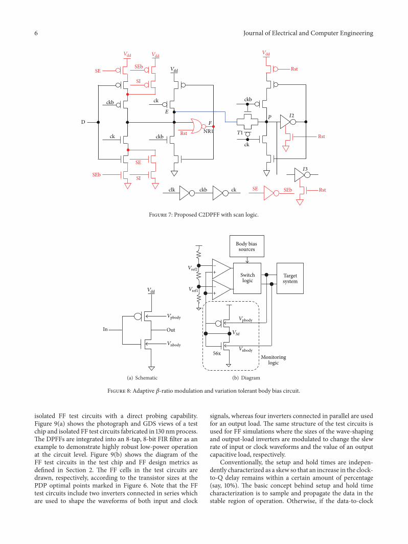
Both proposed DPFFs can be extended to include scanlogic. For example, Figure 7 shows one possible implemen-tation of the scanned C2DPFF which, same as the scannedTGDPFF, includes total of 36 transistors and functions as ascanned asynchronous reset D-type FF.
5. Adaptive Body Bias Technique for UltralowVoltage Operation
Due to the impact of process variation and skewness betweenthe PMOS and NMOS transistors, circuit robustness canseverely degrade especially for subthreshold operation. Thislimits supply voltage scaling while providing proper logicfunctionality with limited voltage headroom under processvariation. Hence, it is of primary essence to keep an equaldevice strength ratio between the transistors in the FFs as wellas logic cells tominimize the impact of process variation [28].
Weproposed a circuit technique,ABRM(adaptive𝛽-ratiomodulation) [29, 30], which dynamically adjusts the P/N-ratio (or 𝛽-ratio) in the current drive between the PMOSand NMOS transistors and thus maximizes noise margin andcircuit robustness for ultradynamic voltage operation. Forreader’s convenience, we restate a brief explanation of ABRMas follows.
The body bias technique is used to equalize the strengthof pull-up and pull-down networks when switching back andforth between different regions of operation (Figure 8(a)).Forward body bias (FBB) lowers 𝑉
𝑇, whereas reverse body
bias (RBB) increases 𝑉𝑇. Body biases are implemented with
additional body-biasing rails for PMOS and NMOS transis-tors (namely, 𝑉pbody and 𝑉nbody) and a body bias generatingcircuit.
Figure 8(b) shows the body bias circuit for ABRM. Theproposed adaptive body bias generator (BBG) consists oftwo comparators, switch logic, body bias voltage sources,two reference voltage sources, and an inverter to monitorthe logical threshold voltage 𝑉
𝑀. The monitored 𝑉
𝑀of the
inverter is compared against the reference voltages of 𝑉ref1and 𝑉ref2. If 𝑉𝑀 is below a predetermined reference potential(𝑉ref1), indicating that the NMOS transistor is stronger thanthe PMOS transistor, we apply a FBB to the pull-up network(PUN) and/or a RBB to the pull-down network (PDN) tomake them equally strong. Conversely, if the monitored 𝑉
𝑀
is higher than 𝑉ref2, the 𝛽-ratio is too large compared to theoptimal value due to strong PMOS. We apply a FBB to thePDN (and/or a RBB to the PUN). If 𝑉
𝑀is monitored to be
between the two reference levels, zero body bias (ZBB) isapplied to the target system.The generated BB voltages are fedto the inverter, and then the updated 𝑉
𝑀is again compared
against the reference voltages. With more voltage references(i.e., fine-grained levels), this loop repeats until the best BBvoltages are found.
6. Results and Discussions
To compare FF features among the conventional FFs andproposed DPFFs in terms of design metrics, we implement
6 Journal of Electrical and Computer Engineering
E
FD
SE
SE
SE
Rst
Rst
Rst
Rst
SEb
SEb
SEb
SI
SI
NR1
P
T1
I2
I3
Vdd
VddVddVdd
clk
ckb
ckb
ckb
ckbck
ck
ck
ck
Figure 7: Proposed C2DPFF with scan logic.
Vpbody
Vnbody
In Out
Vdd
(a) Schematic
Vref2
Vref1
−
+
−
+
Body biassources
Switchlogic
VM
56xMonitoring
logic
Targetsystem
Vpbody
Vnbody
(b) Diagram
Figure 8: Adaptive 𝛽-ratio modulation and variation tolerant body bias circuit.
isolated FF test circuits with a direct probing capability.Figure 9(a) shows the photograph and GDS views of a testchip and isolated FF test circuits fabricated in 130 nmprocess.The DPFFs are integrated into an 8-tap, 8-bit FIR filter as anexample to demonstrate highly robust low-power operationat the circuit level. Figure 9(b) shows the diagram of theFF test circuits in the test chip and FF design metrics asdefined in Section 2. The FF cells in the test circuits aredrawn, respectively, according to the transistor sizes at thePDP optimal points marked in Figure 6. Note that the FFtest circuits include two inverters connected in series whichare used to shape the waveforms of both input and clock
signals, whereas four inverters connected in parallel are usedfor an output load. The same structure of the test circuits isused for FF simulations where the sizes of the wave-shapingand output-load inverters are modulated to change the slewrate of input or clock waveforms and the value of an outputcapacitive load, respectively.
Conventionally, the setup and hold times are indepen-dently characterized as a skew so that an increase in the clock-to-Q delay remains within a certain amount of percentage(say, 10%). The basic concept behind setup and hold timecharacterization is to sample and propagate the data in thestable region of operation. Otherwise, if the data-to-clock

Journal of Electrical and Computer Engineering 7
Technology: 130nm CMOSChip size: 4mm × 5mm
BB g
ener
ator 8-tap FIR
FF test circuits
(a) Photograph and GDS layout view
D0
ck
Wave shaping
D Q
FF
clk
Output load
D
clk
Q
tsetupthold
tclk2q
(b) FF test circuits
Figure 9: Test chip with isolated FF test circuits in 130 nm technology.
Table 1: Conventional FFs versus proposed DPFFs (measured).
Param. MTGFF C2FF C2DPFF TGDPFF𝑡clk2qh [ps] 185 172 136 142𝑡clk2ql [ps] 174 169 130 139𝑡setup [ps] 57 43 46 54𝑡hold [ps] 49 44 45 48𝑃tot [𝜇W] 2.290 2.041 1.846 1.815𝑃leakh [nW] 3.060 1.885 1.766 1.757𝑃leakl [nW] 2.868 2.252 1.804 1.714Area [𝜇m2] 122.21 77.91 77.65 74.21Test condition: SS/1.15 V/25∘C for delay and power.Test condition: FF/1.25 V/125∘C for leakage.
skew (or time difference) is too small then a FF fails to capturethe data or fails to correctly transfer the data. The windowof data-to-clock skew is termed as the failure region. Duringtiming analysis the constraints ensure that the FF does notfall into the failure region. In the stable region, the nominalclock-to-Q delay is named 𝑡0clk2q.
Table 1 summarizes the average values of 97 sets of thereferential and proposed FFs, measured from the isolatedtest circuits shown in Figure 9 at the slow-slow (SS) cornerwith a supply voltage of 1.15 V and 25∘C for delay and powerconsumption and at the fast-fast (FF) corner with a supplyvoltage of 1.25V and 125∘C for leakage characterization. Thearea is calculated without scan logic. It can be seen that,compared with the MTGFF, both proposed DPFFs achievea considerable improvement in the clock-to-Q delay by more
Table 2: Delay sensitivity over 𝑉dd variation (measured).
Voltage [V] Clock-to-Q rise/fall delay [ns]MTGFF C2FF C2DPFF TGDPFF
1.15 0.185/0.174 0.172/0.1692 0.136/0.130 0.142/0.1391.10 0.208/0.197 0.198/0.1911 0.155/0.149 0.165/0.1621.05 0.237/0.227 0.229/0.2199 0.179/0.174 0.195/0.1911.00 0.279/0.265 0.262/0.2580 0.210/0.208 0.236/0.2290.95 0.331/0.317 0.318/0.3018 0.250/0.240 0.288/0.2810.90 0.411/0.393 0.392/0.3825 0.316/0.322 0.365/0.3580.85 0.525/0.514 0.532/0.5094 0.417/0.431 0.482/0.4790.80 0.726/0.716 0.746/0.7058 0.658/0.674 0.671/0.6810.75 1.091/1.086 1.126/1.0961 0.962/1.011 0.978/1.0250.70 1.916/1.864 1.975/1.8429 1.674/1.704 1.649/1.7110.65 3.543/3.448 3.657/3.4009 2.954/2.807 2.905/2.853Ratio 19.1/19.8 21.2/20.1 21.7/21.5 20.4/20.5Test condition: SS/25∘C.Ratio (%) = delay at 0.65V/delay at 1.15 V.
than 20% due to the reduced logic depth, which in turn mayallow the direct path applied FFs to achieve further reductionin area and power consumption. Note that the use of C2MOSinverter at the primary input stage of the C2FF and C2DPFFlowers the setup time by 25% and 19%, respectively, over theMTGFF. Improvement in the delay and setup time apparentlyrelaxes the timing constraints and improves performance oftarget systems.
Table 2 shows delay variation over supply voltage scalingof the conventional and proposed FFs, measured at the SS

8 Journal of Electrical and Computer Engineering
D
Q 36mV
60mV
Figure 10: Waveforms of the C2DPFF at 60mV (measured).
corner with a supply voltage range of 1.15 V to 0.65V and−25∘C, where the delay ratio or sensitivity is calculated asa ratio of the delay at 0.65V over the delay at 1.15 V. It canbe observed that the proposed DPFFs have comparable delaysensitivity over supply voltage scaling with the conventionalFFs especially at low voltages.
Figure 10 shows the input 𝐷 and output 𝑄 waveformsmeasured from the C2DPFF in the deep subthreshold region.The measured minimum supply voltage of 𝑉dd,min = 60mVresults in the dynamic switching power of 24.7 pW, five ordersofmagnitude smaller than normal voltage operation, with theminimum-sized design at an operating frequency of 50Hzduring ten complete binary cycles (i.e., low-to-high and high-to-low transitions). On the other hand, 𝑉dd,min of 80mV and85mV is measured for the conventional C2FF and MTGFF,respectively. It is worthwhile to mention that the output ofa 36mV swing is observed at a supply voltage of 𝑉dd =60mV. This voltage diminution is due to the fact that, unlikein the normal 𝑉dd region, the OFF leakage current is notnegligible anymore compared to the (operating) subthresholdcurrent in the ultralow 𝑉dd region. That is, 𝐼sub/𝐼off ∼ 10
2
for 𝑉dd < 𝑉𝑇, whereas 𝐼on/𝐼off ∼ 105 for 𝑉dd > 𝑉𝑇,
where 𝐼on is the (normal) ON current, 𝐼sub is the subthresholdcurrent, 𝐼off is the leakage current, and 𝑉
𝑇is the threshold
voltage of the device. The main conduction current at highor normal 𝑉dd’s can be explained by the drift mechanismwhile the subthreshold current at ultralow 𝑉dd’s is mainlygoverned by the diffusion mechanism. For example, assumethat the input 𝐷 is set to “1” and a “0” value is driven to theinternal node 𝑃 in Figure 4.Then, the PMOS transistor of theoutput driver I3 must pull up the output to 𝑉dd by overridingthe (idle) OFF current of the NMOS transistor of I3. If thePMOS operating current is not strong enough to overcometheNMOSOFF current (unlike at high𝑉dd’s), a supply voltageis divided resistively across the transistors and, as a result, theoutput will not rise all the way to 𝑉dd in deep subthresholdoperations.
Many studies have been reported regarding the theoreti-cal and practical limit of CMOS logic operation [26, 31, 32].Presentation of astonishing circuit operation at aggressively
scaled supply voltages (i.e., 36mV swing at a supply voltageof 60mV) does not necessarily mean that it is recommendedto operate the system at the voltage level but to providemeasurement results as an evidence of increased circuitrobustness with the proposed technique and as a possibleadvantage of the body bias technique to lower 𝑉dd,min andsalvage a silicon chip; otherwise, a circuit would fail to operatedue to the presence of various process variations.
Comparison of the FF types in the clock-to-Q delayrequires consideration of negative as well as positive influ-ences. As discussed in Section 4, the reduced logic depthalong the main signal propagation path usually decreases thepropagation delay, whereas the use of the C2MOS invertergenerally comes with the stacking effect which results inhigher threshold voltage and less current drive and thusincreases the propagation delay. In comparison of C2FF withMTGFF, delay decrease tendency thanks to the reduced logicdepth compensates delay increase due to the stacking effectand hence the delay of the C2FF is comparable to or slightlybetter than that of the MTGFF.
In the proposed DPFFs, however, much reduced logicdepth further lowers the clock-to-Q delay by roughly oneand two inverter delays over C2FF and MTGFF, respectively,surpassing a feasible delay increase caused by the stackingeffect. This is the best advantage of the DPFFs where thedirect path connection considerably improves the clock-to-Qdelay by 17% over the conventional FFs. From the power andarea perspective, this gate delay improvement can providean opportunity to save more power at the isoperformancecondition even with less area. Moreover, direct path connec-tion allows the use of minimum-sized transistors in the data-storing units (e.g., I1 and I2 in Figure 4) that are now onthe noncritical path, providing a further reduction in area,dynamic, and leakage powers by more than 36% (0.3%), 19%(9%), and 37% (6%) over the MTGFF (C2FF), respectively,with the same output load. Note that, in the C2FF, the outputdriver I2 drives the feedback transistors,M1 andM2, as wellas the underlying output load, which decreases the outputslope especially in the presence of large fanout. The C2DPFFandTGDPFF address this fanout issue by using the additionaldriver I3 and I4, respectively, dedicated to drive output as inMTGFF, which improves the output slope and current driveof the cell, covering a wide range of fanout.
Figure 11 now provides the measurement results with var-ious signal polarities and driving strengths. The normalizedaverage values of the MTGFF, C2FF, TGDPFF, and C2DPFFare plotted in red, black, magenta, and blue, respectively. Asthe setup skew becomes smaller, the contamination delay,the amount of time needed for a change in a logic input tocause an initial change at an output, dramatically increases.Consequently, there is a radical push out in the clock-to-Q delay as shown in the figure. Note that, for a certainclock-to-Q delay, the hold time increases with a decrease inthe setup time to keep the internal race immunity in (2).One may argue that the DPFFs cause an increase in thesetup and hold times as side effects. This is due to the factthat the decreased nominal clock-to-Q delay lowers the 10%constraint as well, which increases the setup and hold timesby their definition; even the absolute values almost remain

Journal of Electrical and Computer Engineering 9
sel_sub
VCO Level-downshifter
Vddgen.
BBG
VM monitoring block
BBsource
Vref
clkVdd VddH
2
2 Vp,nbody
In 0
In 1
.
.
....
In 7
Leve
l-dow
n sh
ifter
8
8 8
8
8 8
8
16 16 16 16
16
Sub-VT
F/F
Sub-VT
F/F
Sub-VT
F/F
Sub-VT
F/F
Z−1
Z−1
C1 C8
1st tap 8th tap
8-tap FIR filter
· · ·
Leve
l-up
shift
er
Out 0
Out 1
Out 15
+ +
Figure 11: The FIR filter.
the same.The authors believe that the FFs should be designedto operate with margin in the nominal delay region (i.e.,the flat region in Figure 11) for stable and prompt operation.The increased setup and hold times are acceptable and fullyredeemed by considerable advantages in propagation delay,power consumption, and area.
The proposed DPFFs are fully integrated into an 8 × 8FIR filter fabricated in 130 nm technology. Figure 11 shows thearchitecture of the 8-tap, 8-bit FIR filter. Detailed discussionsof the filter are found in [29, 30]. With the application ofABRM by which the optimal 𝛽-ratio value of the filter isautomatically driven by the BBG (body bias generator) asshown in Figure 9, the filter successfully operates all the waydown to 85mV, consuming 40 nW of power at an operatingfrequency of 240Hz. This ultralow voltage operation proveshigh circuit robustness of the DPFFs since relative variationsare significantly higher with voltage scaling and the circuitbecomes much more vulnerable to noise disturbance withlimited voltage headroom.
7. Conclusions
Design metrics are of primary importance for the FFs to beused as primitive library cells. We proposed two direct pathmaster-slave FFs which adopt a C2MOS style input buffer toimprove performance while providing full compatibility withwidely used EDA characterization tools. Internal direct pathbetween the master and slave latches reduces the logic depthalong themain signal path, achieving a further speedup in thepropagation delay. Measurements from the ABRM-appliedtest circuits fabricated in 130 nm demonstrated potentialadvantages of the proposed FFs in designmetrics for ultralowas well as normal voltage applications.
Competing Interests
The authors declare that they have no competing interests.
Acknowledgments
This work has been supported by the 2014 Research Fund ofUniversity of Ulsan.
References
[1] H. Kawaguchi and T. Sakurai, “A reduced clock-swing flip-flop(RCSFF) for 63% power reduction,” IEEE Journal of Solid-StateCircuits, vol. 33, no. 5, pp. 807–811, 1998.
[2] G. Gerosa, S. Gary, C. Dietz et al., “A 2.2W 80 MHz superscalarRISC microprocessor,,” IEEE Journal of Solid-State Circuits, vol.29, no. 12, pp. 1440–1454, 1994.
[3] U. Ko and P. T. Balsara, “High-performance energy-efficient D-flip-flop circuits,” IEEE Transactions on Very Large Scale Inte-gration (VLSI) Systems, vol. 8, no. 1, pp. 94–98, 2000.
[4] J. Yuan and C. Svensson, “High-performance energy-efficientD-flip-flop circuits,” IEEE Journal of Solid-State Circuits, vol. 24,no. 1, pp. 62–70, 1989.
[5] J. M. Rabaey, A. P. Chandrakasan, and B. Nikolic, Digital Inte-grated Circuits: A Design Perspective, chapter 7, Prentice Hall,Upper Saddle River, NJ, USA, 2nd edition, 2003.
[6] T. Ishikawa, M. Kinugasa, and M. Kida, “Master-slave clockedCMOS flip-flop with hysteresis,” US Patent, No. US5107137A,April 1992.
[7] B. Nikolic, V. G. Oklobdzija, V. Stojanovic, W. Jia, J. K.-S. Chiu,andM.M.-T. Leung, “Improved sense-amplifier-based flip-flop:design and measurements,” IEEE Journal of Solid-State Circuits,vol. 35, no. 6, pp. 876–884, 2000.

10 Journal of Electrical and Computer Engineering
[8] V. Zyuban, “Optimization of scannable latches for low energy,”IEEE Transactions on Very Large Scale Integration (VLSI) Sys-tems, vol. 11, no. 5, pp. 778–788, 2003.
[9] F. Ricci, L. T. Clark, T. Beatty et al., “A 1.5 GHz 90 nm embeddedmicroprocessor core,” in Proceednigs of the VLSI Circuits, Digestof Technical Papers, vol. 15, pp. 12–15, Kyoto, Japan, June 2005.
[10] K. Absel, L. Manuel, and R. K. Kavitha, “Low-power dual dyn-amic node pulsed hybrid flip-flop featuring efficient embeddedlogic,” IEEE Transactions on Very Large Scale Integration (VLSI)Systems, vol. 21, no. 9, pp. 1693–1704, 2013.
[11] V. Stojanovic and V. G. Oklobdzija, “Comparative analysis ofmaster-slave latches and flip-flops for high-performance andlow-power systems,” IEEE Journal of Solid-State Circuits, vol. 34,no. 4, pp. 536–548, 1999.
[12] M. Alioto, E. Consoli, and G. Palumbo, “Analysis and com-parison in the energy-delay-area domain of nanometer CMOSFlip-Flops: part I—methodology and design strategies,” IEEETransactions on Very Large Scale Integration (VLSI) Systems, vol.19, no. 5, pp. 725–736, 2011.
[13] H. Partovi, R. Burd, U. Salim, F. Weber, L. DiGregorio, andD. Draper, “Flow-through latch and edge-triggered flip-flophybrid elements,” in Proceedings of the IEEE International Solid-State Circuits Conference, Digest of Technical Papers, pp. 138–139, San Francisco, Calif, USA, February 1996.
[14] F. Klass, “Semi-dynamic and dynamic flip-flops with embeddedlogic,” in Proceedings of the Symposium on VLSI Circuits. Digestof Technical Papers, pp. 108–109, Honolulu, Hawaii, USA, June1998.
[15] S. Hesley, V. Andrade, B. Burd et al., “A 7th-generation x86microprocessor,” in Proceedings of the IEEE International Solid-State Circuits Conference, Digest of Technical Papers, pp. 92–93,San Francisco, Calif, USA, February 1999.
[16] C. F. Webb, C. J. Anderson, L. Sigal et al., “A 400-MHz S/390microprocessor,” IEEE Journal of Solid-State Circuits, vol. 32, no.11, pp. 1665–1675, 1997.
[17] Y. Zhang, H. Yang, and H. Wang, “Low clock-swing con-ditional-precharge flip-flop for more than 30% power reduc-tion,” Electronics Letters, vol. 36, no. 9, pp. 785–786, 2000.
[18] B.-S. Kong, S.-S. Kim, and Y.-H. Jun, “Conditional-capture flip-flop for statistical power reduction,” IEEE Journal of Solid-StateCircuits, vol. 36, no. 8, pp. 1263–1271, 2001.
[19] N. Nedovic, M. Aleksic, and V. Oklobdzija, “Conditional tech-niques for small power consumption flip-flops,” in Proceedingsof the IEEE International Conference on Electronics, Circuits &Systems (CAS ’01), pp. 803–806, Malta, Spain, September 2001.
[20] M. Tokumasu, H. Fujii, M. Ohta, T. Fuse, and A. Kameyama,“A new reduced clock-swing flip-flop: NAND-type Keeper flip-flop (NDKFF),” in Proceedings of the IEEE Custom IntegratedCircuits Conference, pp. 129–132, Orlando, Fla, USA, May 2002.
[21] A. Ma and K. Asanovic, “A double-pulsed set-conditional-resetflip-flop,” MIT LCS Technical Report MIT-LCS-TR-844, 2002.
[22] Cadence, Encounter Library Characterizer, Cadence, 2013.[23] Synopsys, “SiliconSmart,” July 2013, http://www.synopsys.com.[24] Synopsys, “Liberty NCX,” 2013, http://www.synopsys.com.[25] Altos Design Automation, Liberate User Guide, Ver.2.4, 2009.[26] A. Bryant, J. Brown, P. Cottrell, M. Ketchen, J. Ellis-Monaghan,
and E. J. Nowak, “Low-power CMOS at Vdd = 4kT/q,” in Pro-ceedings of the Device Research Conference, pp. 22–23, NotreDame, Ind, USA, June 2001.
[27] M. E. Hwang, S. O. Jung, and K. Roy, “Slope interconnecteffort: gate-interconnect interdependent delay modeling for
early CMOS circuit simulation,” IEEE Transactions on Circuitsand Systems I: Regular Papers, vol. 56, no. 7, pp. 1428–1441, 2008.
[28] A. Bryant, J. Brown, P. Cottrell, M. Ketchen, J. Ellis-Monaghan,and E. J. Nowak, “Low-power CMOS at Vdd = 4kT/q,” inDeviceResearch Conference, pp. 22–23, Notre Dame, Ind, USA, June2001.
[29] M.-E. Hwang, “ABRM: adaptive 𝛽-ratio modulation for pro-cess-tolerant ultradynamic voltage scaling,” IEEE Transactionson Very Large Scale Integration (VLSI) Systems, vol. 18, no. 2, pp.281–290, 2010.
[30] M.-E. Hwang, A. Raychowdhury, K. Kim, and K. Roy, “A 85mV40 nW process-tolerant subthreshold 8x8 FIR filter in 130 nmtechnology,” in Proceedings of the IEEE Symposium on VLSICircuits (VLSI ’07), pp. 154–155, Kyoto, Japan, June 2007.
[31] S. Vangal and S. Jain, “Claremont: a solar-powered near-threshold voltage IA-32 processor,” in Design Technologies forGreen and Sustainable Computing Systems, P. P. Pande, A.Ganguly, and K. Chakrabarty, Eds., chapter 9, pp. 229–239,Springer, New York, NY, USA, 2013.
[32] E. J. Nowak, “Maintaining the benefits of CMOS scaling whenscaling bogs down,” IBM Journal of Research and Development,vol. 46, no. 2-3, pp. 169–180, 2002.

International Journal of
AerospaceEngineeringHindawi Publishing Corporationhttp://www.hindawi.com Volume 2014
RoboticsJournal of
Hindawi Publishing Corporationhttp://www.hindawi.com Volume 2014
Hindawi Publishing Corporationhttp://www.hindawi.com Volume 2014
Active and Passive Electronic Components
Control Scienceand Engineering
Journal of
Hindawi Publishing Corporationhttp://www.hindawi.com Volume 2014
International Journal of
RotatingMachinery
Hindawi Publishing Corporationhttp://www.hindawi.com Volume 2014
Hindawi Publishing Corporation http://www.hindawi.com
Journal ofEngineeringVolume 2014
Submit your manuscripts athttp://www.hindawi.com
VLSI Design
Hindawi Publishing Corporationhttp://www.hindawi.com Volume 2014
Hindawi Publishing Corporationhttp://www.hindawi.com Volume 2014
Shock and Vibration
Hindawi Publishing Corporationhttp://www.hindawi.com Volume 2014
Civil EngineeringAdvances in
Acoustics and VibrationAdvances in
Hindawi Publishing Corporationhttp://www.hindawi.com Volume 2014
Hindawi Publishing Corporationhttp://www.hindawi.com Volume 2014
Electrical and Computer Engineering
Journal of
Advances inOptoElectronics
Hindawi Publishing Corporation http://www.hindawi.com
Volume 2014
The Scientific World JournalHindawi Publishing Corporation http://www.hindawi.com Volume 2014
SensorsJournal of
Hindawi Publishing Corporationhttp://www.hindawi.com Volume 2014
Modelling & Simulation in EngineeringHindawi Publishing Corporation http://www.hindawi.com Volume 2014
Hindawi Publishing Corporationhttp://www.hindawi.com Volume 2014
Chemical EngineeringInternational Journal of Antennas and
Propagation
International Journal of
Hindawi Publishing Corporationhttp://www.hindawi.com Volume 2014
Hindawi Publishing Corporationhttp://www.hindawi.com Volume 2014
Navigation and Observation
International Journal of
Hindawi Publishing Corporationhttp://www.hindawi.com Volume 2014
DistributedSensor Networks
International Journal of