2: the mcf51jm microcontroller - aet.calu.eduaet.calu.edu/~jsumey/cet360/ppts/02-coldfire.pdf ·...
TRANSCRIPT

2: The MCF51JM Microcontroller
CET360 Microprocessor Engineering 1
2:The MCF51JM Microcontroller
CET360Microprocessor Engineering
J. Sumeyver. 1/30/18
2
MCF51JM Overview
32-bit ColdFire (V1) MCU w/ USB 2.7~5.5V, up to 50 MHz
descendent of the 68000 (68k) family, now a NXP product same register set
based on high-performance RISC CPU 32-bit data bus, PC, registers, ALU! 24-bit address bus 2-stage pipelines for each instructions and operands 2 operational modes: user, supervisor
extensive library of on-board peripheral modules multiple operational modes single-wire background debug capability (BDM)

2: The MCF51JM Microcontroller
CET360 Microprocessor Engineering 2
3
MCF51JM Modules
Memory: Flash (128KB), RAM (16KB) ACMP: analog comparator ADC: 12-bit analog-to-digital (12 channels) BDM: background debug support, single-wire CAN: controller area network CMT: carrier modulator timer COP: computer operating properly IIC: inter-integrated circuit serial bus KBI: keyboard interrupt (8 inputs) LVD: low voltage detector MCG: multipurpose clock generator GPIO: I/O ports (51 GP + 6 Rapid GP pins) RTC: real-time counter SCI, SPI: serial interfaces (2 SCI, 2 SPI) TPM: timer/pulse-width modulator (6+2 channels) USBOTG: host/device support (dual-role)
4
2: The MCF51JM Microcontroller
CET360 Microprocessor Engineering 3
5
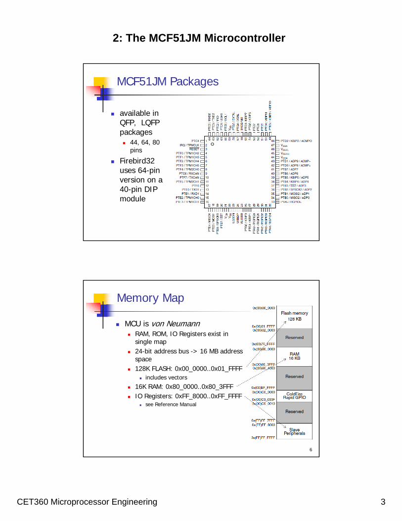
MCF51JM Packages
available in QFP, LQFP packages 44, 64, 80
pins
Firebird32 uses 64-pin version on a 40-pin DIP module
6
Memory Map
MCU is von Neumann RAM, ROM, IO Registers exist in
single map 24-bit address bus -> 16 MB address
space 128K FLASH: 0x00_0000..0x01_FFFF
includes vectors
16K RAM: 0x80_0000..0x80_3FFF IO Registers: 0xFF_8000..0xFF_FFFF
see Reference Manual

2: The MCF51JM Microcontroller
CET360 Microprocessor Engineering 4
• performs all computation / instruction execution
(CFPRM ColdFire Programmer’s Ref. Manual)
ColdFire CPU
Programming Model – User Mode
16 general-purpose 32-bit registers (8 Data + 8 Address) 32-bit program counter, PC (top 8 bits forced to zero) 8-bit condition code register, CCR A7 doubles as SP this is User mode, Supervisor mode has additional registers…
8
Condition Code Register
X: sign extendN: Negative flagZ: Zero flagV: signed overflowC: unsigned overflow

2: The MCF51JM Microcontroller
CET360 Microprocessor Engineering 5
Programming Model - Supervisor
adds additional CPU registers for "privileged" operations
MCF51JM includes: 16-bit status register, SR (CCR is lower byte) supervisor SP, OTHER_A7 VBR sets base address of vector table (defaults to 0)
9
Status Register (SR) Details
system byte only available in supervisor mode T: 1=trace enable S: 0=user mode, 1=supervisor mode M: 1=master state, 0=interrupt state I: sets interrupt mask level 0..7
0 = all interrupts enabled 1 = all interrupts disabled (except IRQ pin)
10
2: The MCF51JM Microcontroller
CET360 Microprocessor Engineering 6
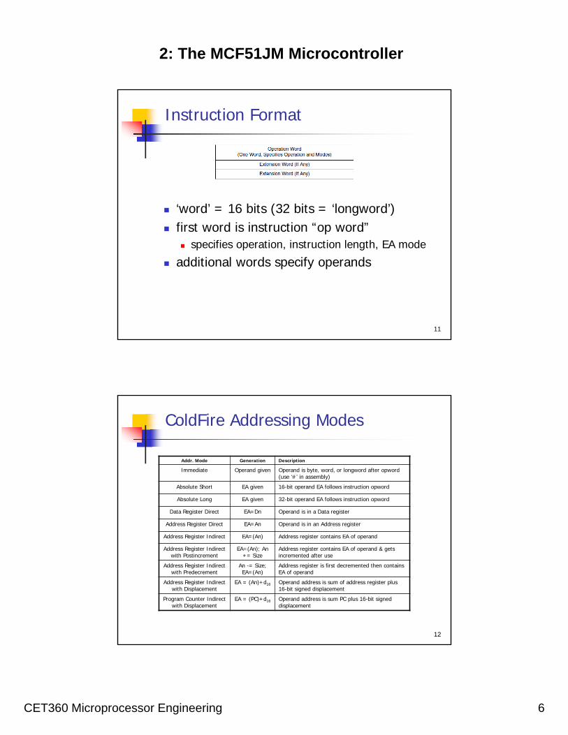
Instruction Format
‘word’ = 16 bits (32 bits = ‘longword’) first word is instruction “op word”
specifies operation, instruction length, EA mode
additional words specify operands
11
12
ColdFire Addressing Modes
Addr. Mode Generation Description
Immediate Operand given Operand is byte, word, or longword after opword(use ‘#’ in assembly)
Absolute Short EA given 16-bit operand EA follows instruction opword
Absolute Long EA given 32-bit operand EA follows instruction opword
Data Register Direct EA=Dn Operand is in a Data register
Address Register Direct EA=An Operand is in an Address register
Address Register Indirect EA=(An) Address register contains EA of operand
Address Register Indirect with Postincrement
EA=(An); An += Size
Address register contains EA of operand & gets incremented after use
Address Register Indirect with Predecrement
An -= Size; EA=(An)
Address register is first decremented then contains EA of operand
Address Register Indirect with Displacement
EA = (An)+d16 Operand address is sum of address register plus 16-bit signed displacement
Program Counter Indirect with Displacement
EA = (PC)+d16 Operand address is sum PC plus 16-bit signed displacement
2: The MCF51JM Microcontroller
CET360 Microprocessor Engineering 7
ColdFire Instruction Set Summary
organized by type of operation data movement program control integer arithmetic floating-point arithmetic (when FPU available) logical operations shift operations bit manipulation system control cache maintenance
13
• provides interface to general purpose I/O pins
(MCF51JM ColdFire Ref. Manual, ch. 9)
Parallel I/O Ports
2: The MCF51JM Microcontroller
CET360 Microprocessor Engineering 8
I/O Ports
up to 70 i/o pins on up to 9 ports named A..I
each 8-bit port has i/o register and DDR also have pull-up, slew rate, drive strength, and
interrupt control registers
naming convention: PTxD, PTxDD ex: PTAD, PTEDD ref: table 4-2 in ref. manual
also: individual bit access ex: PTBD_PTBD2 = 1;
15
• provides hardware time counting functions with optional interrupt
(MCF51JM ColdFire Ref. Manual, ch. 17)
Real-Time Counter (RTC) Module

2: The MCF51JM Microcontroller
CET360 Microprocessor Engineering 9
RTC Components
strictly internal, no external pins three input clock sources, software selectable
1 kHz internal low-power oscillator (LPO) 32 kHz internal clock (IRCLK) external clock (ERCLK) – from MCG module
software-programmable prescaler 8-bit up counter with 8-bit modulo match
comparator software controlled interrupt on modulo
match17
RTC Block Diagram
18
shaded boxes represent RTC registers
2: The MCF51JM Microcontroller
CET360 Microprocessor Engineering 10
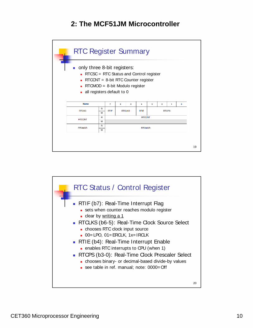
RTC Register Summary
only three 8-bit registers: RTCSC = RTC Status and Control register RTCCNT = 8-bit RTC Counter register RTCMOD = 8-bit Modulo register all registers default to 0
19
RTC Status / Control Register
RTIF (b7): Real-Time Interrupt Flag sets when counter reaches modulo register clear by writing a 1
RTCLKS (b6-5): Real-Time Clock Source Select chooses RTC clock input source 00=LPO, 01=ERCLK, 1x=IRCLK
RTIE (b4): Real-Time Interrupt Enable enables RTC interrupts to CPU (when 1)
RTCPS (b3-0): Real-Time Clock Prescaler Select chooses binary- or decimal-based divide-by values see table in ref. manual; note: 0000=Off
20

2: The MCF51JM Microcontroller
CET360 Microprocessor Engineering 11
RTC Usage Example
msdelay(): a precise ms delay function
requires RTCMOD > 0 this version does not use RTIF leaving the RTC modulo
feature fully available
21
// msdelay(): delay given number of milliseconds using Real-Time Counter modulevoid msdelay(int n){
while (n-- > 0) {byte ctr = RTCCNT; // take copy of current RTC Counter registerwhile (RTCCNT == ctr) {} // wait till it changes
}}
// include in initialization code:RTCSC = 0x08; // enable RTC, select 1ms period from 1kHz internal clock
• prioritizes all system exceptions and performs all vector handling
(MCF51JM Coldfire Ref. Manual, ch. 8 and ColdFire Programmer’s Ref. Manual, ch. 11)
INTerrupt Controller (INTC) Module
2: The MCF51JM Microcontroller
CET360 Microprocessor Engineering 12
23
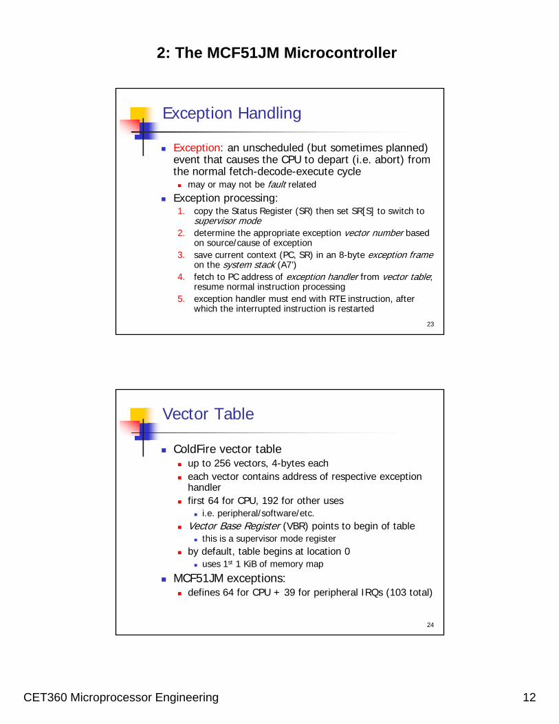
Exception Handling
Exception: an unscheduled (but sometimes planned) event that causes the CPU to depart (i.e. abort) from the normal fetch-decode-execute cycle may or may not be fault related
Exception processing:1. copy the Status Register (SR) then set SR[S] to switch to
supervisor mode2. determine the appropriate exception vector number based
on source/cause of exception3. save current context (PC, SR) in an 8-byte exception frame
on the system stack (A7’)4. fetch to PC address of exception handler from vector table;
resume normal instruction processing5. exception handler must end with RTE instruction, after
which the interrupted instruction is restarted
Vector Table
ColdFire vector table up to 256 vectors, 4-bytes each each vector contains address of respective exception
handler first 64 for CPU, 192 for other uses
i.e. peripheral/software/etc. Vector Base Register (VBR) points to begin of table
this is a supervisor mode register by default, table begins at location 0
uses 1st 1 KiB of memory map
MCF51JM exceptions: defines 64 for CPU + 39 for peripheral IRQs (103 total)
24
2: The MCF51JM Microcontroller
CET360 Microprocessor Engineering 13
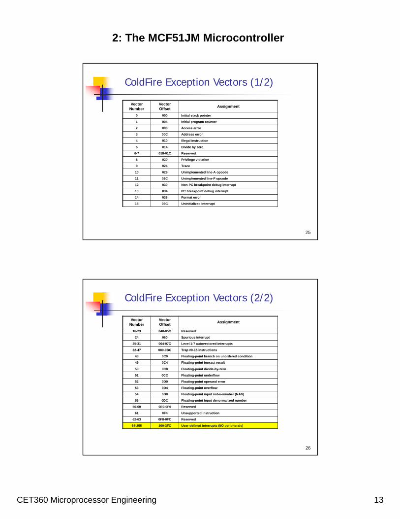
VectorNumber
VectorOffset
Assignment
0 000 Initial stack pointer
1 004 Initial program counter
2 008 Access error
3 00C Address error
4 010 Illegal instruction
5 014 Divide by zero
6-7 018-01C Reserved
8 020 Privilege violation
9 024 Trace
10 028 Unimplemented line-A opcode
11 02C Unimplemented line-F opcode
12 030 Non-PC breakpoint debug interrupt
13 034 PC breakpoint debug interrupt
14 038 Format error
15 03C Uninitialized interrupt
ColdFire Exception Vectors (1/2)
25
VectorNumber
VectorOffset
Assignment
16-23 040-05C Reserved
24 060 Spurious interrupt
25-31 064-07C Level 1-7 autovectored interrupts
32-47 080-0BC Trap #0-15 instructions
48 0C0 Floating-point branch on unordered condition
49 0C4 Floating-point inexact result
50 0C8 Floating-point divide-by-zero
51 0CC Floating-point underflow
52 0D0 Floating-point operand error
53 0D4 Floating-point overflow
54 0D8 Floating-point input not-a-number (NAN)
55 0DC Floating-point input denormalized number
56-60 0E0-0F0 Reserved
61 0F4 Unsupported instruction
62-63 0F8-0FC Reserved
64-255 100-3FC User-defined interrupts (I/O peripherals)
ColdFire Exception Vectors (2/2)
26

2: The MCF51JM Microcontroller
CET360 Microprocessor Engineering 14
VectorNumber
VectorOffset
Assignment
64 100 IRQ (pin)
65 104 Low Voltage Detect
66 108 Loss of Lock
67 10C SPI1
68 110 SPI2
69 114 USB_Status
70 118 -
71 11C TPM1 Channel 0
72 120 TPM1 Channel 1
73 124 TPM1 Channel 2
74 128 TPM1 Channel 3
75 12C TPM1 Channel 4
76 130 TPM1 Channel 5
77 134 TPM1 Overflow
78 138 TPM2 Channel 0
79 13C TPM2 Channel 1
80 140 TPM2 Overflow
MCF51JM Exceptions (1/2)
27
VectorNumber
VectorOffset
Assignment
81 144 SCI1 Error
82 148 SCI1 Receive
83 14C SCI1 Transmit
84 150 SCI2 Error
85 154 SCI2 Receive
86 158 SCI2 Transmit
87 15C KBI Interrupt
88 160 ADC Conversion
89 164 ACMP
90 168 IIC1
91 16C RTC
92 170 IIC2
93 174 CMT
94 178 CAN Wakeup
95 17C CAN Error
96 180 CAN Receive
97 184 CAN Transmit
98 188 RNGA Error
104-110 1A0-1BC Force_lvli (i=7..1)
MCF51JM Exceptions (2/2)
28

2: The MCF51JM Microcontroller
CET360 Microprocessor Engineering 15
Interrupt Dispositions
some interrupts are non-maskable but most are maskable programmer can enable / disable at will
CPU CCR contains a 3-bit interrupt priority field for controlling maskable interrupts 0..7, any level below current setting is disabled resets to 7
CodeWarrior’s hidef.h file contains relevant macros EnableInterrupts: sets level to 0 DisableInterrupts: sets level to 7
derivative.h defines all vector numbers ex:
29
#define VectorNumber_Vrtc 91U
Spoiler alert! (how to program an ISR)
ex: an ISR to handle RTC interrupts must also enable interrupts in the RTCSC register,
i.e. RTIE must be set!
ISRs can neither accept or return arguments "interrupt" causes '}' to be an RTE instead of RTS
and respective interrupt vector to be setup
30
// rtc_isr(): process interrupts from RTC moduleinterrupt VectorNumber_Vrtc void rtc_isr(void){
RTCSC_RTIF = 1; // acknowledge & reset RTIF flag// process RTC event – timekeeping, update LEDs, etc.
⋮}

2: The MCF51JM Microcontroller
CET360 Microprocessor Engineering 16
• a highly flexible peripheral module used to perform timing-related
tasks in hardware
(MCF51JM ColdFire Ref. Manual, ch. 22)
Timer/PWM (TPM) Module
32
TPM Features
two TPMs TPM1 has 6 channels, TPM2 has 2
optionally uses PortE,F bits for external I/O input capture
measure characteristics of input pulses/signals
output compare generation of programmer-defined signals pulse/periodic, frequency, duty cycle
powerful interrupt capabilities

2: The MCF51JM Microcontroller
CET360 Microprocessor Engineering 17
33
TPM Components
16-bit binary up counter driven by BUSCLK thru with programmable prescaler 8 choices: 1 .. 128
up to 8 channels, ea. 16-bits, programmable for input capture (IC) or output compare (OC) operation
PWM generation capability
set of control/status registers
TPM Block Diagram
2: The MCF51JM Microcontroller
CET360 Microprocessor Engineering 18
35
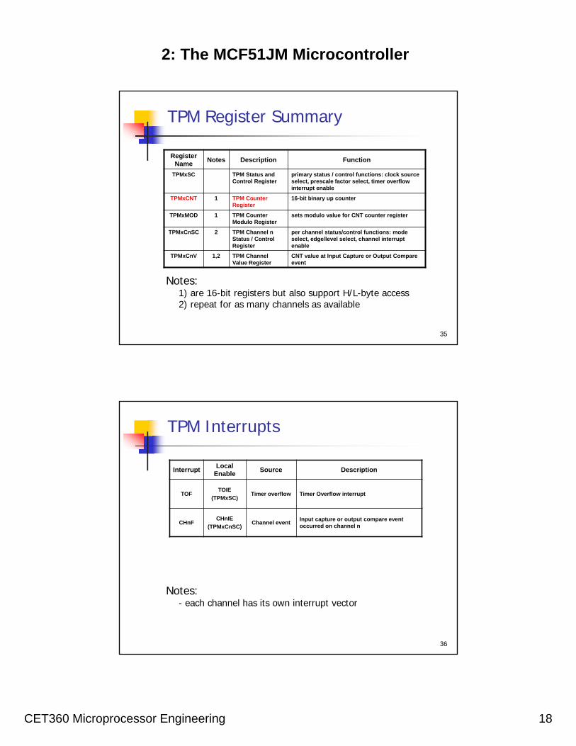
TPM Register Summary
RegisterName
Notes Description Function
TPMxSC TPM Status and Control Register
primary status / control functions: clock source select, prescale factor select, timer overflow interrupt enable
TPMxCNT 1 TPM Counter Register
16-bit binary up counter
TPMxMOD 1 TPM Counter Modulo Register
sets modulo value for CNT counter register
TPMxCnSC 2 TPM Channel n Status / Control Register
per channel status/control functions: mode select, edge/level select, channel interrupt enable
TPMxCnV 1,2 TPM Channel Value Register
CNT value at Input Capture or Output Compare event
Notes:1) are 16-bit registers but also support H/L-byte access2) repeat for as many channels as available
36
TPM Interrupts
InterruptLocal
EnableSource Description
TOFTOIE
(TPMxSC)Timer overflow Timer Overflow interrupt
CHnFCHnIE
(TPMxCnSC)Channel event
Input capture or output compare event occurred on channel n
Notes:- each channel has its own interrupt vector

2: The MCF51JM Microcontroller
CET360 Microprocessor Engineering 19
• a peripheral module providing 28 channels of 8-, 10- or 12-bit A/D conversion
(MCF51JM ColdFire Ref. Manual, ch. 21)
ADC Module
38
ADC Features
28 input channels (12 externally available) 8-, 10- or 12-bit resolution right justified, unsigned result selectable ADC clock conversion time under 2 us possible! per command or continuous conversion modes internal temperature sensor
one interrupt source conversion complete

2: The MCF51JM Microcontroller
CET360 Microprocessor Engineering 20
39
ADC Module Components
conversion clock selection & prescaler 32 inputs via analog multiplexer successive approx. register (SAR) compare function interrupt logic
40
ADC Block Diagram

2: The MCF51JM Microcontroller
CET360 Microprocessor Engineering 21
ADC Register Map
41
Address Offset
Register Name
Function Description
0x0000 ADCSC1 Status and Control Register 1selects channel, conversion mode, interrupt enable; provides conversion complete status (COCO)
0x0001 ADCSC2 Status and Control Register 2 sets conversion trigger and compare features
0x0002 ADCRH Data Result High Register top 2 (10-bit) or 4 (12-bit) bits of ADC result
0x0003 ADCRL Data Result Low Register bottom 8 bits of ADC result
0x0004 ADCCVH Compare Value High Register high byte of compare value (when enabled)
0x0005 ADCCVL Compare Value Low Register low byte of compare value (when enabled)
0x0006 ADCCFG Configuration Register selects ADC clocking, sample time, # bits (8,10,12)
0x0007 APCTL1 Pin Control 1 Register disables pin I/O control, channels 0-7
0x0008 APCTL2 Pin Control 1 Register disables pin I/O control, channels 8-15
Above addresses are offsets from ADC base address (0xFFFF8010).
ADC Channel Assignments (MCF51)
42
ADCH* Channel Input
00000 AD0 PTB0/MISO2/ADP0
00001 AD1 PTB1/MOSI2/ADP1
00010 AD2 PTB2/SPSCK2/ADP2
00011 AD3 PTB3/SS2/ADP3
00100 AD4 PTB4/KBIP4/ADP4
00101 AD5 PTB5/KBIP5/ADP5
00110 AD6 PTB6/ADP6
00111 AD7 PTB7/ADP7
01000 AD8 PTD0/ADP8/ACMP+
01001 AD9 PTD1/ADP9/ACMP-
01010 AD10 PTD3/KBIP3/ADP10
01011 AD11 PTD4/ADP11
01100 AD12 VREFL
01101 AD13 VREFL
01110 AD14 VREFL
01111 AD15 VREFL
ADCH* Channel Input
10000 AD16 VREFL
10001 AD17 VREFL
10010 AD18 VREFL
10011 AD19 VREFL
10100 AD20 VREFL
10101 AD21 VREFL
10110 AD22 Reserved
10111 AD23 Reserved
11000 AD24 Reserved
11001 AD25 Reserved
11010 AD26 Temperature Sensor
11011 AD27 Internap bandgap
11100 - Reserved
11101 VREFH VDD
11110 VREFL VSS
11111 ADC off None
*bottom 5 bits written to the ADCSC1 register
2: The MCF51JM Microcontroller
CET360 Microprocessor Engineering 22
43
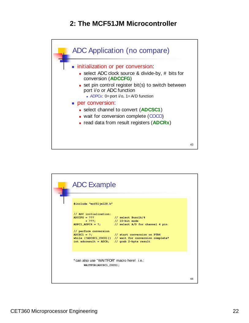
ADC Application (no compare)
initialization or per conversion: select ADC clock source & divide-by, # bits for
conversion (ADCCFG) set pin control register bit(s) to switch between
port i/o or ADC function ADPCx: 0=port i/o, 1=A/D function
per conversion: select channel to convert (ADCSC1) wait for conversion complete (COCO) read data from result registers (ADCRx)
44
ADC Example
#include “mcf51jm128.h”
// ADC initialization:ADCCFG = ??? // select Busclk/4
+ ???; // 10-bit modeADPC1_ADPC4 = ?; // select A/D for channel 4 pin
// perform conversionADCSC1 = ?; // start conversion on PTB4while (!ADCSC1_COCO){} // wait for conversion complete*int adcresult = ADCR; // grab 2-byte result
*can also use “WAITFOR” macro here! i.e.:WAITFOR(ADCSC1_COCO);

2: The MCF51JM Microcontroller
CET360 Microprocessor Engineering 23
• implements full duplex, asynchronous serial communication at programmed
baud rates with framing
(MCF51JM ColdFire Ref. Manual, ch. 12)
SCI Module
46
SCI Features
configurable baud rate supports standard asynchronous rates
8- or 9-bit data format for multi-node communications
receiver error detection parity, noise, framing errors
10 interrupt events although shared through 3 common vectors
uses pins on Ports C,E most MCF members have multiple SCIs!
implements a total of 7 r/w registers

2: The MCF51JM Microcontroller
CET360 Microprocessor Engineering 24
47
SCI Components
13-bit baud rate divider determines data rate for both Tx & Rx
transmitter w/ 11-bit PISO shift register serializes output data to TxD with framing parity generator 2 interrupt events shared on SCI Transmit vector
receiver w/ 11-bit SIPO shift register deserializes input data from RxD 4 rx interrupt events on SCI Receive vector 4 error events on SCI Error vector
48
SCI Transmitter Block Diagram

2: The MCF51JM Microcontroller
CET360 Microprocessor Engineering 25
49
SCI
Rece
iver
Bl
ock
Dia
gram
50
SCI Register Map
SCI1 base address = 0xFFFF8038 SCI2 base address = 0xFFFF8040
Address Offset
Register Name
Description
0 SCIxBDH SCI Baud rate register High
1 SCIxBDL SCI Baud rate register Low
2 SCIxC1 SCI Control Register 1
3 SCIxC2 SCI Control Register 2
4 SCIxS1 SCI Status Register 1
5 SCIxS2 SCI Status Register 2
6 SCIxC3 SCI Control Register 3
7 SCIxD SCI Data Register (Tx/Rx)
Above addresses are offsets from SCI base address.

2: The MCF51JM Microcontroller
CET360 Microprocessor Engineering 26
51
Baud Rate Setting
baud rate is determined from BUSCLK and13 SBR bits divider in Baud rate register:SCI Baud = BUSCLK / (16 • SBR[12:0]) example SBR values:
BaudBUSCLK =
12MHz% Error
BUSCLK = 16MHz
% Error
2400 313 -0.16 417 -0.08
4800 156 0.16 208 0.16
9600 78 0.16 104 0.16
19200 39 0.16 52 0.16
38400 20 -2.34 26 0.16
52
“Non Return to Zero”
format determined by SCIxC1 bits:
M: mode (0=“1/8/1”, 1=“1/9/1”) PE: parity enable (0=off, 1=on) PT: parity type (0=even, 1=odd)
NRZ Serial Data Format
LOOPS SCISW RSRC M Wake ILT PE PT
7 6 5 4 3 2 1 0
2: The MCF51JM Microcontroller
CET360 Microprocessor Engineering 27
53
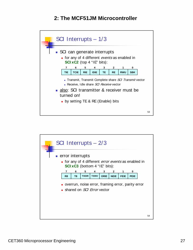
SCI Interrupts – 1/3
SCI can generate interrupts for any of 4 different events as enabled in
SCIxC2 (top 4 “IE” bits):
Transmit, Transmit Complete share SCI Transmit vector Receive, Idle share SCI Receive vector
also: SCI transmitter & receiver must be turned on! by setting TE & RE (Enable) bits
TIE TCIE RIE IDIE TE RE RWU SBK
7 6 5 4 3 2 1 0
54
SCI Interrupts – 2/3
error interrupts for any of 4 different error events as enabled in
SCIxC3 (bottom 4 “IE” bits):
overrun, noise error, framing error, parity error shared on SCI Error vector
R8 T8 TXDIR TXINV ORIE NEIE FEIE PEIE
7 6 5 4 3 2 1 0

2: The MCF51JM Microcontroller
CET360 Microprocessor Engineering 28
55
SCI Interrupts – 3/3
ISR must check SCIxS1 to determine cause of interrupt and react appropriately (only for multiple enabled events) top 4 bits…
bottom 4 bits reflect error status of previously received character
TDRE TC RDRF IDLE OR NF FE PF
7 6 5 4 3 2 1 0
56
SCI Operation – 1/2
initialization write baud registers set baud rate
SCIxBDH first, then SCIxBDL can also just write 16 bit word to SCIxBD
write SCIxC1 to set data format write SCIxC2 to turn on SCI & enable Tx/Rx
interrupts as appropriate optional: write SCIxC3 to turn on error interrupts
if needed also make sure SCI vectors are setup if using
SCI interrupts!

2: The MCF51JM Microcontroller
CET360 Microprocessor Engineering 29
57
SCI Code: Initialization
activate SCI for 9600 baud (at 16 MHz bus) (and no interrupts)
// SCI initialize routinevoid SCI1_init(){
SCI1BD = ???; // set baud rateSCI1C1 = ???; // no special settings neededSCI1C2 = ???; // enable Tx & Rx
}
58
SCI Operation – 2/2
transmission wait for transmitter empty
TDRE=1 of SCIxS1
write new character to SCIxD
reception wait for character to be received
RDRF=1 in SCIxS1
read received char from SCIxD
Note: this approach will “block” the CPU! what if blocking is not desired?
2: The MCF51JM Microcontroller
CET360 Microprocessor Engineering 30
59
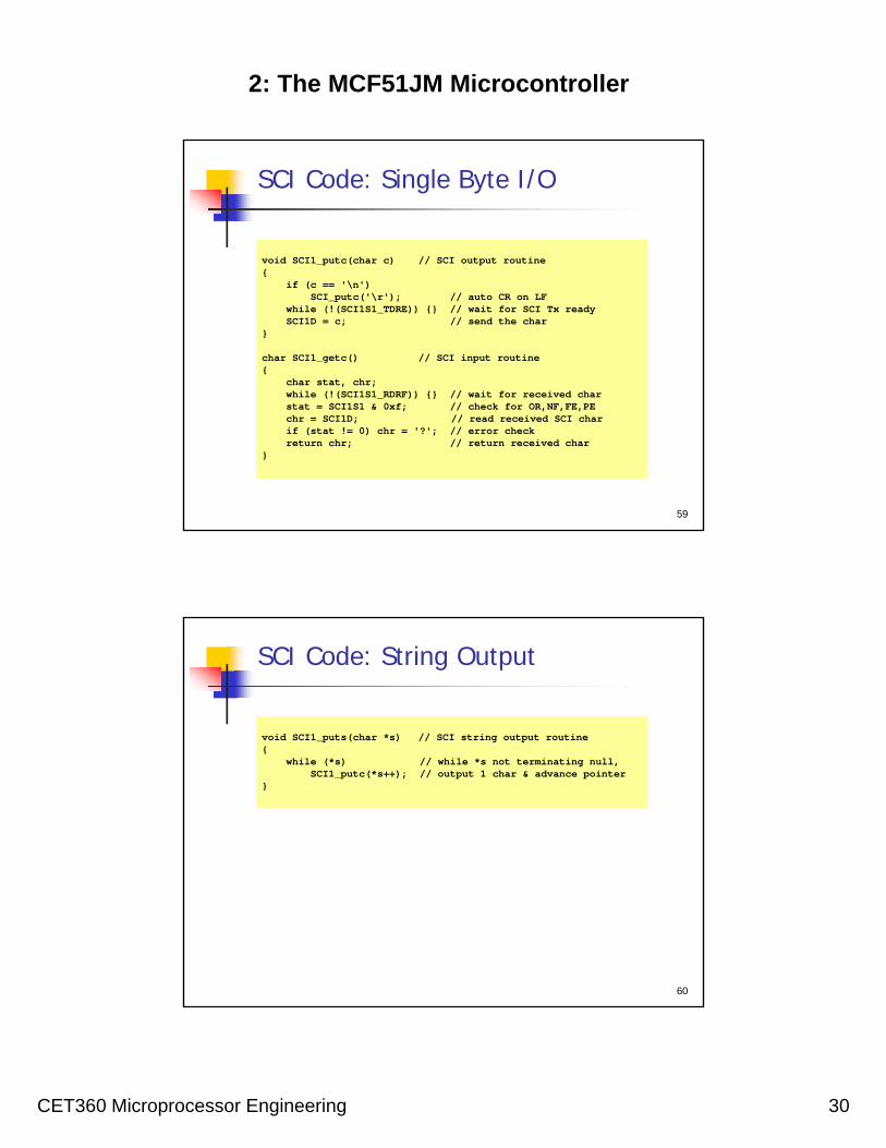
SCI Code: Single Byte I/O
void SCI1_putc(char c) // SCI output routine{
if (c == '\n')SCI_putc('\r'); // auto CR on LF
while (!(SCI1S1_TDRE)) {} // wait for SCI Tx readySCI1D = c; // send the char
}
char SCI1_getc() // SCI input routine{
char stat, chr;while (!(SCI1S1_RDRF)) {} // wait for received charstat = SCI1S1 & 0xf; // check for OR,NF,FE,PEchr = SCI1D; // read received SCI charif (stat != 0) chr = '?'; // error checkreturn chr; // return received char
}
60
SCI Code: String Output
void SCI1_puts(char *s) // SCI string output routine{
while (*s) // while *s not terminating null,SCI1_putc(*s++); // output 1 char & advance pointer
}