2003agrawal: digital test and dft1 fundamentals of digital test and dft vishwani d. agrawal rutgers...
Post on 20-Dec-2015
217 views
TRANSCRIPT
2003 Agrawal: Digital Test and DFT 1
Fundamentals of Digital Test and DFT
Fundamentals of Digital Test and DFT
Vishwani D. AgrawalRutgers University, Dept. of ECE
New Jersey
http://cm.bell-labs.com/cm/cs/who/va
January 2003

2003 Agrawal: Digital Test and DFT 2
Course OutlineCourse Outline
Basic concepts and definitions Fault modeling Fault simulation ATPG DFT and scan design BIST Boundary scan IDDQ test

2003 Agrawal: Digital Test and DFT 3
VLSI Realization ProcessVLSI Realization Process
Determine requirements
Write specifications
Design synthesis and Verification
FabricationManufacturing test
Chips to customer
Customer’s need
Test development

2003 Agrawal: Digital Test and DFT 4
DefinitionsDefinitions
Design synthesis: Given an I/O function, develop a procedure to manufacture a device using known materials and processes.
Verification: Predictive analysis to ensure that the synthesized design, when manufactured, will perform the given I/O function.
Test: A manufacturing step that ensures that the physical device, manufactured from the synthesized design, has no manufacturing defect.

2003 Agrawal: Digital Test and DFT 5
Realities of TestsRealities of Tests
Based on analyzable fault models, which may not map onto real defects.
Incomplete coverage of modeled faults due to high complexity.
Some good chips are rejected. The fraction (or percentage) of such chips is called the yield loss.
Some bad chips pass tests. The fraction (or percentage) of bad chips among all passing chips is called the defect level.

2003 Agrawal: Digital Test and DFT 6
Costs of TestingCosts of Testing Design for testability (DFT)
Chip area overhead and yield reduction Performance overhead
Software processes of test Test generation and fault simulation Test programming and debugging
Manufacturing test Automatic test equipment (ATE) capital cost Test center operational cost

2003 Agrawal: Digital Test and DFT 7
Cost of Manufacturing Testing in 2000AD
Cost of Manufacturing Testing in 2000AD
0.5-1.0GHz, analog instruments,1,024 digital pins: ATE purchase price = $1.2M + 1,024 x $3,000 = $4.272M
Running cost (five-year linear depreciation) = Depreciation + Maintenance + Operation
= $0.854M + $0.085M + $0.5M = $1.439M/year
Test cost (24 hour ATE operation) = $1.439M/(365 x 24 x 3,600) = 4.5 cents/second

2003 Agrawal: Digital Test and DFT 8
Present and Future*Present and Future*
Transistors/sq. cm 4 - 10M 18 - 39M
Pin count 100 - 900 160 - 1475
Clock rate (MHz) 200 - 730 530 - 1100
Power (Watts) 1.2 - 61 2 - 96
Feature size (micron) 0.25 - 0.15 0.13 - 0.10
1997--2001 2003--2006
* SIA Roadmap, IEEE Spectrum, July 1999
2003 Agrawal: Digital Test and DFT 9
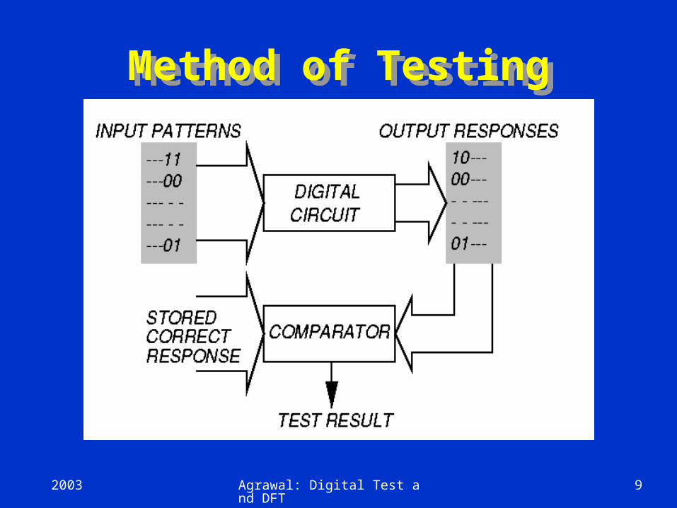
Method of TestingMethod of Testing

2003 Agrawal: Digital Test and DFT 10
ADVANTEST Model T6682 ATE
ADVANTEST Model T6682 ATE

2003 Agrawal: Digital Test and DFT 11
LTX FUSION HF ATELTX FUSION HF ATE

2003 Agrawal: Digital Test and DFT 12
VLSI Chip YieldVLSI Chip Yield A manufacturing defect is a finite chip area with
electrically malfunctioning circuitry caused by errors in the fabrication process.
A chip with no manufacturing defect is called a good chip.
Fraction (or percentage) of good chips produced in a manufacturing process is called the yield. Yield is denoted by symbol Y.
Cost of a chip:
Cost of fabricating and testing a wafer-------------------------------------------------------
-------------Yield x Number of chip sites on the
wafer

2003 Agrawal: Digital Test and DFT 13
Defect Level or Reject RatioDefect Level or Reject Ratio
Defect level (DL) is the ratio of faulty chips among the chips that pass tests.
DL is measured as parts per million (ppm). DL is a measure of the effectiveness of tests. DL is a quantitative measure of the
manufactured product quality. For commercial VLSI chips a DL greater than 500 ppm is considered unacceptable.

2003 Agrawal: Digital Test and DFT 14
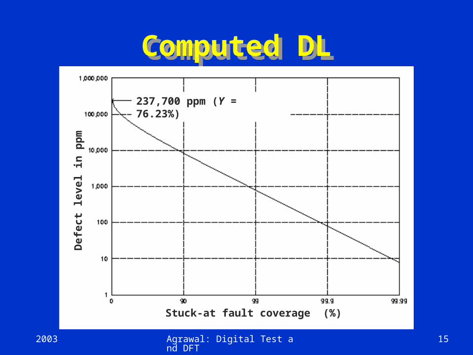
Example: SEMATECH ChipExample: SEMATECH Chip
Bus interface controller ASIC fabricated and tested at IBM, Burlington, Vermont
116,000 equivalent (2-input NAND) gates 304-pin package, 249 I/O Clock: 40MHz, some parts 50MHz 0.45 CMOS, 3.3V, 9.4mm x 8.8mm area Full scan, 99.79% fault coverage Advantest 3381 ATE, 18,466 chips tested at
2.5MHz test clock Data obtained courtesy of Phil Nigh (IBM)
2003 Agrawal: Digital Test and DFT 15
Computed DLComputed DL
Stuck-at fault coverage (%)
Defe
ct
level in
pp
m
237,700 ppm (Y = 76.23%)

2003 Agrawal: Digital Test and DFT 16
Summary: IntroductionSummary: Introduction VLSI Yield drops as chip area increases; low yield
means high cost Fault coverage measures the test quality Defect level (DL) or reject ratio is a measure of chip
quality DL can be determined by an analysis of test data For high quality: DL < 500 ppm, fault coverage ~
99%

2003 Agrawal: Digital Test and DFT 17
Fault ModelingFault Modeling

2003 Agrawal: Digital Test and DFT 18
Why Model Faults?Why Model Faults?
I/O function tests inadequate for manufacturing (functionality versus component and interconnect testing)
Real defects (often mechanical) too numerous and often not analyzable
A fault model identifies targets for testing A fault model makes analysis possible Effectiveness measurable by experiments
2003 Agrawal: Digital Test and DFT 19
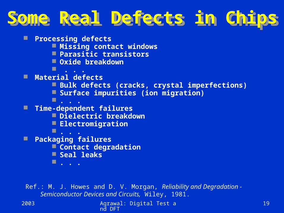
Some Real Defects in ChipsSome Real Defects in Chips Processing defects
Missing contact windows Parasitic transistors Oxide breakdown . . .
Material defects Bulk defects (cracks, crystal imperfections) Surface impurities (ion migration) . . .
Time-dependent failures Dielectric breakdown Electromigration . . .
Packaging failures Contact degradation Seal leaks . . .
Ref.: M. J. Howes and D. V. Morgan, Reliability and Degradation - Semiconductor Devices and Circuits, Wiley, 1981.

2003 Agrawal: Digital Test and DFT 20
Observed PCB DefectsObserved PCB DefectsDefect classes
ShortsOpensMissing componentsWrong componentsReversed componentsBent leadsAnalog specificationsDigital logicPerformance (timing)
Occurrence frequency (%)
51 1 613 6 8 5 5 5
Ref.: J. Bateson, In-Circuit Testing, Van Nostrand Reinhold, 1985.
2003 Agrawal: Digital Test and DFT 21
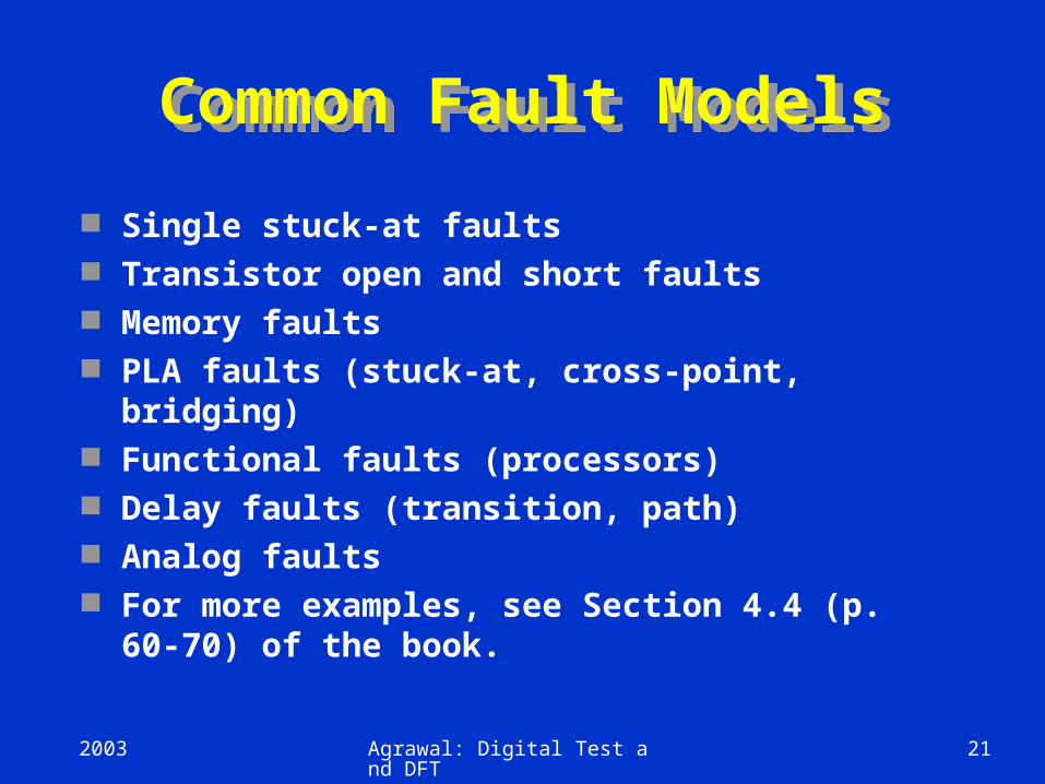
Common Fault ModelsCommon Fault Models
Single stuck-at faults Transistor open and short faults Memory faults PLA faults (stuck-at, cross-point,
bridging) Functional faults (processors) Delay faults (transition, path) Analog faults For more examples, see Section 4.4 (p.
60-70) of the book.

2003 Agrawal: Digital Test and DFT 22
Single Stuck-at FaultSingle Stuck-at Fault Three properties define a single stuck-at fault
Only one line is faulty The faulty line is permanently set to 0 or 1 The fault can be at an input or output of a gate
Example: XOR circuit has 12 fault sites ( ) and 24 single stuck-at faults
a
b
c
d
e
f
1
0
g h i 1
s-a-0j
k
z
0(1)1(0)
1
Test vector for h s-a-0 fault
Good circuit valueFaulty circuit value

2003 Agrawal: Digital Test and DFT 23
Fault EquivalenceFault Equivalence Number of fault sites in a Boolean gate circuit =
#PI + #gates + #(fanout branches). Fault equivalence: Two faults f1 and f2 are
equivalent if all tests that detect f1 also detect f2. If faults f1 and f2 are equivalent then the
corresponding faulty functions are identical. Fault collapsing: All single faults of a logic circuits
can be divided into disjoint equivalence subsets, where all faults in a subset are mutually equivalent. A collapsed fault set contains one fault from each equivalence subset.
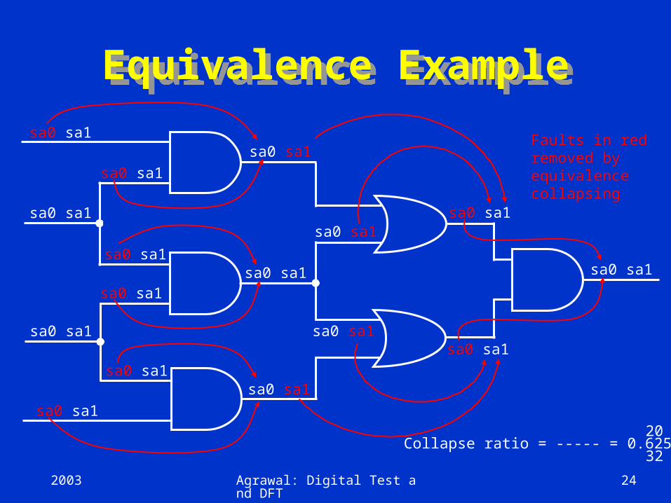
2003 Agrawal: Digital Test and DFT 24
Equivalence ExampleEquivalence Example
sa0 sa1sa0 sa1
sa0 sa1
sa0 sa1
sa0 sa1
sa0 sa1
sa0 sa1
sa0 sa1
sa0 sa1
sa0 sa1
sa0 sa1
sa0 sa1
sa0 sa1
sa0 sa1
sa0 sa1
sa0 sa1
Faults in redremoved byequivalencecollapsing
20Collapse ratio = ----- = 0.625 32
2003 Agrawal: Digital Test and DFT 25
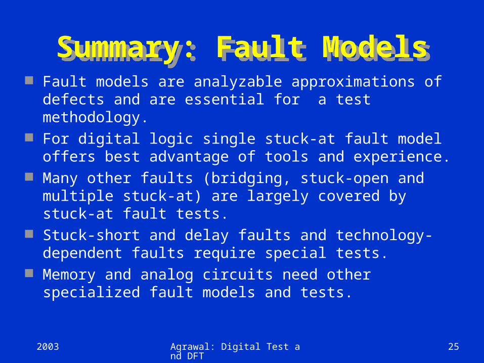
Summary: Fault ModelsSummary: Fault Models Fault models are analyzable approximations of
defects and are essential for a test methodology. For digital logic single stuck-at fault model offers
best advantage of tools and experience. Many other faults (bridging, stuck-open and
multiple stuck-at) are largely covered by stuck-at fault tests.
Stuck-short and delay faults and technology-dependent faults require special tests.
Memory and analog circuits need other specialized fault models and tests.

2003 Agrawal: Digital Test and DFT 26
Fault SimulationFault Simulation

2003 Agrawal: Digital Test and DFT 27
Problem and MotivationProblem and Motivation Fault simulation Problem: Given
A circuit A sequence of test vectors A fault model
Determine Fault coverage - fraction (or percentage) of modeled
faults detected by test vectors Set of undetected faults
Motivation Determine test quality and in turn product quality Find undetected fault targets to improve tests

2003 Agrawal: Digital Test and DFT 28
Fault simulator in a VLSI Design ProcessFault simulator in a VLSI Design Process
Verified designnetlist
Verificationinput stimuli
Fault simulator Test vectors
Modeledfault list
Testgenerator
Testcompactor
Faultcoverage
?
Remove tested faults
Deletevectors
Add vectors
Low
Adequate
Stop

2003 Agrawal: Digital Test and DFT 29
Fault Simulation Scenario
Fault Simulation Scenario
Circuit model: mixed-level Mostly logic with some switch-level for high-impedance
(Z) and bidirectional signals High-level models (memory, etc.) with pin faults
Signal states: logic Two (0, 1) or three (0, 1, X) states for purely Boolean
logic circuits Four states (0, 1, X, Z) for sequential MOS circuits
Timing: Zero-delay for combinational and synchronous circuits Mostly unit-delay for circuits with feedback

2003 Agrawal: Digital Test and DFT 30
Fault Simulation Scenario (continued)
Fault Simulation Scenario (continued)
Faults: Mostly single stuck-at faults Sometimes stuck-open, transition, and path-delay
faults; analog circuit fault simulators are not yet in common use
Equivalence fault collapsing of single stuck-at faults Fault-dropping -- a fault once detected is dropped from
consideration as more vectors are simulated; fault-dropping may be suppressed for diagnosis
Fault sampling -- a random sample of faults is simulated when the circuit is large
2003 Agrawal: Digital Test and DFT 31
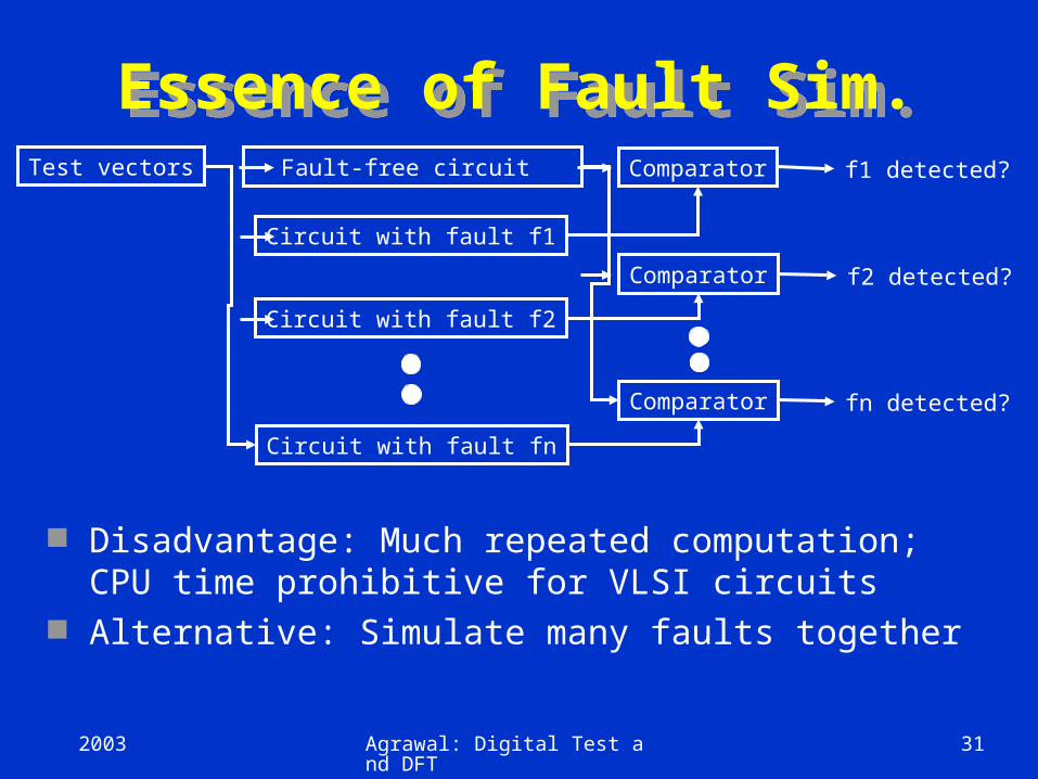
Essence of Fault Sim.Essence of Fault Sim.
Disadvantage: Much repeated computation; CPU time prohibitive for VLSI circuits
Alternative: Simulate many faults together
Test vectors Fault-free circuit
Circuit with fault f1
Circuit with fault f2
Circuit with fault fn
Comparator f1 detected?
Comparator f2 detected?
Comparator fn detected?

2003 Agrawal: Digital Test and DFT 32
Fault SamplingFault Sampling
A randomly selected subset (sample) of faults is simulated.
Measured coverage in the sample is used to estimate fault coverage in the entire circuit.
Advantage: Saving in computing resources (CPU time and memory.)
Disadvantage: Limited data on undetected faults.

2003 Agrawal: Digital Test and DFT 33
Random Sampling Model
Random Sampling Model
All faults witha fixed butunknowncoverage
Detectedfault
Undetectedfault
Random
picking
Np = total number of faults
(population size)
C = fault coverage (unknown)
Ns = sample size
Ns << Npc = sample coverage (a random variable)

2003 Agrawal: Digital Test and DFT 34
Probability Density of Sample Coverage, c
Probability Density of Sample Coverage, c (x--C )2
-- ------------ 1 2 2
p (x ) = Prob(x < c < x +dx ) = -------------- e 2 1/2
p (
x )
C C +3C -3 1.0x
Sample coverage
C (1 - C)Variance2 = ------------ Ns
Mean = C
Samplingerror
x
2003 Agrawal: Digital Test and DFT 35
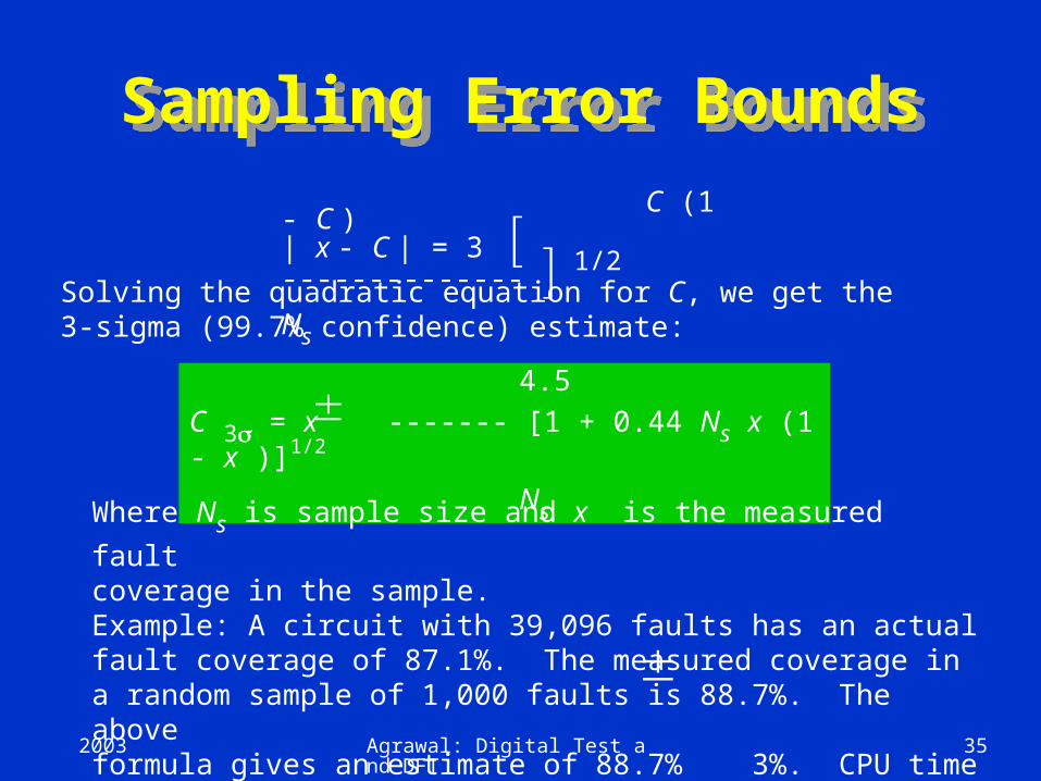
Sampling Error BoundsSampling Error Bounds C (1 - C ) | x - C | = 3 -------------- 1/2
NsSolving the quadratic equation for C, we get the3-sigma (99.7% confidence) estimate:
4.5C 3 = x ------- [1 + 0.44 Ns x (1 - x )]1/2
Ns
Where Ns is sample size and x is the measured fault
coverage in the sample.Example: A circuit with 39,096 faults has an actualfault coverage of 87.1%. The measured coverage ina random sample of 1,000 faults is 88.7%. The aboveformula gives an estimate of 88.7% 3%. CPU time for sample simulation was about 10% of that for all faults.

2003 Agrawal: Digital Test and DFT 36
Summary: Fault Sim.Summary: Fault Sim.
Fault simulator is an essential tool for test development. Concurrent fault simulation algorithm offers the best choice. For restricted class of circuits (combinational and
synchronous sequential with only Boolean primitives), differential algorithm can provide better speed and memory efficiency (Section 5.5.6.)
For large circuits, the accuracy of random fault sampling only depends on the sample size (1,000 to 2,000 faults) and not on the circuit size. The method has significant advantages in reducing CPU time and memory needs of the simulator.

2003 Agrawal: Digital Test and DFT 37
Automatic Test-pattern Generation (ATPG)
Automatic Test-pattern Generation (ATPG)

2003 Agrawal: Digital Test and DFT 38
Functional vs. Structural ATPGFunctional vs.
Structural ATPG

2003 Agrawal: Digital Test and DFT 39
Functional vs. Structural(Continued)
Functional vs. Structural(Continued)
Functional ATPG – generate complete set of tests for circuit input-output combinations 129 inputs, 65 outputs: 2129 = 680,564,733,841,876,926,926,749,
214,863,536,422,912 patterns Using 1 GHz ATE, would take 2.15 x 10²² years
Structural test: No redundant adder hardware, 64 bit slices Each with 27 faults (using fault equivalence) At most 64 x 27 = 1728 faults (tests) Takes 0.000001728 s on 1 GHz ATE
Designer gives small set of functional tests – augment with structural tests to boost coverage to 98+ %
2003 Agrawal: Digital Test and DFT 40
Random-Pattern Generation
Random-Pattern Generation
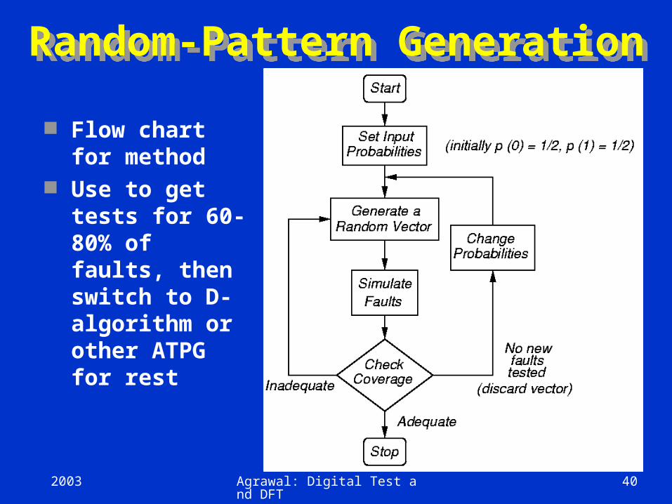
Flow chart for method
Use to get tests for 60-80% of faults, then switch to D-algorithm or other ATPG for rest
2003 Agrawal: Digital Test and DFT 41
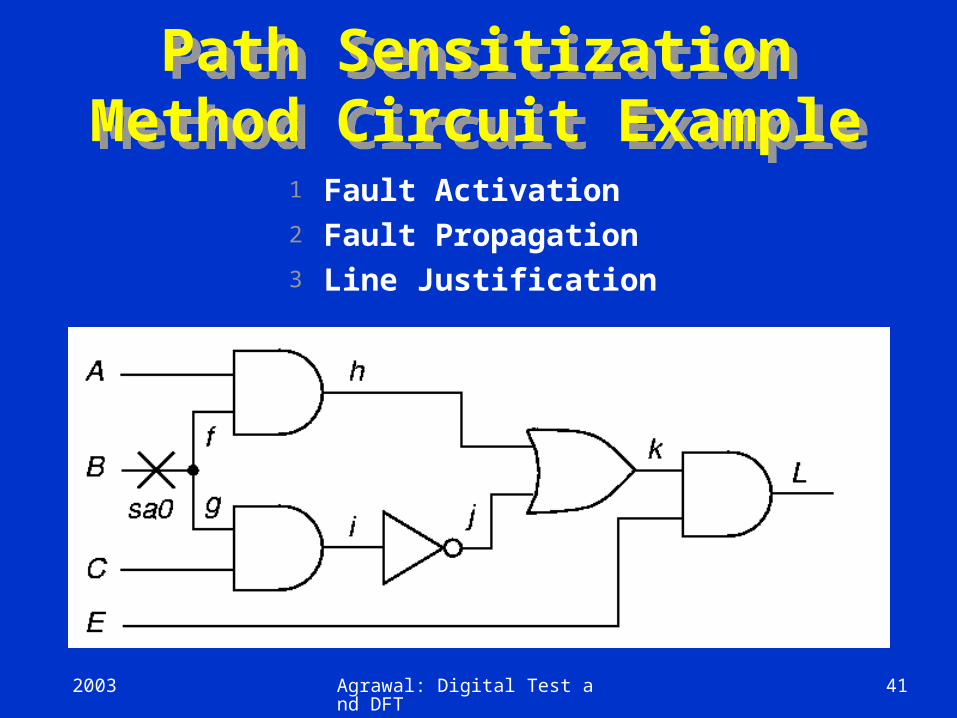
Path Sensitization Method Circuit Example
Path Sensitization Method Circuit Example
1 Fault Activation2 Fault Propagation3 Line Justification

2003 Agrawal: Digital Test and DFT 42
Path Sensitization Method Circuit Example
Path Sensitization Method Circuit Example Try path f – h – k – L blocked at j, since
there is no way to justify the 1 on i
10
D
D1
1
1DD
D
2003 Agrawal: Digital Test and DFT 43
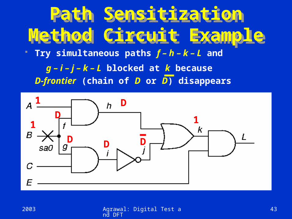
Path Sensitization Method Circuit Example
Path Sensitization Method Circuit Example Try simultaneous paths f – h – k – L and
g – i – j – k – L blocked at k because D-frontier (chain of D or D) disappears
1
DD D
DD
1
1

2003 Agrawal: Digital Test and DFT 44
Path Sensitization Method Circuit Example
Path Sensitization Method Circuit Example Final try: path g – i – j – k – L – test found!
0
D D D
1 DD
1
0
1

2003 Agrawal: Digital Test and DFT 45
Sequential CircuitsSequential Circuits
A sequential circuit has memory in addition to combinational logic.
Test for a fault in a sequential circuit is a sequence of vectors, which
Initializes the circuit to a known state Activates the fault, and Propagates the fault effect to a primary output
Methods of sequential circuit ATPG Time-frame expansion methods Simulation-based methods

2003 Agrawal: Digital Test and DFT 46
Concept of Time-Frames
Concept of Time-Frames
If the test sequence for a single stuck-at fault contains n vectors,
Replicate combinational logic block n times Place fault in each block Generate a test for the multiple stuck-at fault
using combinational ATPG with 9-valued logic
Comb.block
Fault
Time-frame
0
Time-frame
-1
Time-frame-n+1
Unknownor given
Init. state
Vector 0Vector -1Vector -n+1
PO 0PO -1PO -n+1
Statevariables
Nextstate

2003 Agrawal: Digital Test and DFT 47
An Example of Seq. ATPGAn Example of Seq. ATPG
FF2
FF1
A
B
s-a-1

2003 Agrawal: Digital Test and DFT 48
Nine-Valued Logic (Muth)0,1, 1/0, 0/1, 1/X, 0/X, X/0, X/1,
X
Nine-Valued Logic (Muth)0,1, 1/0, 0/1, 1/X, 0/X, X/0, X/1,
XA
B
X
X
X
0
s-a-10/1
A
B
0/X 0/X
0/1
X
s-a-1X/1
FF1 FF1
FF2 FF20/1 X/1
Time-frame -1 Time-frame 0

2003 Agrawal: Digital Test and DFT 49
Seq. ATPG ResultsSeq. ATPG Results s1423 s5378 s35932
Total faults 1,515 4,603 39,094
Detected faults 1,414 3,639 35,100
Fault coverage 93.3% 79.1% 89.8%
Test vectors 3,943 11,571 257
CPU time 1.3 hrs. 37.8 hrs. 10.2 hrs.HP J200 256MB
Ref.: M. S. Hsiao, E. M. Rudnick and J. H. Patel, “Dynamic State Traversal for Sequential Circuit Test Generation,” ACM Trans. on Design Automation of Electronic Systems (TODAES), vol. 5, no. 3, July 2000.

2003 Agrawal: Digital Test and DFT 50
Summary: ATPGSummary: ATPG Combinational ATPG is significantly more efficient
than sequential ATPG. Combinational ATPG tools are commercially
available. Design for testability is essential if the circuit is
large (million or more gates) and high fault coverage (~95%) is required.

2003 Agrawal: Digital Test and DFT 51
Design for TestabilityDesign for Testability

2003 Agrawal: Digital Test and DFT 52
DefinitionDefinition
Design for testability (DFT) refers to those design techniques that make test generation and test application cost-effective.
DFT methods for digital circuits: Ad-hoc methods Structured methods:
Scan Partial Scan Built-in self-test (BIST) Boundary scan
DFT method for mixed-signal circuits: Analog test bus

2003 Agrawal: Digital Test and DFT 53
Ad-Hoc DFT MethodsAd-Hoc DFT Methods Good design practices learnt through experience are used as
guidelines: Avoid asynchronous (unclocked) feedback. Make flip-flops initializable. Avoid redundant gates. Avoid large fanin gates. Provide test control for difficult-to-control signals. Avoid gated clocks. . . . Consider ATE requirements (tristates, etc.)
Design reviews conducted by experts or design auditing tools.
Disadvantages of ad-hoc DFT methods: Experts and tools not always available. Test generation is often manual with no guarantee of high
fault coverage. Design iterations may be necessary.
2003 Agrawal: Digital Test and DFT 54
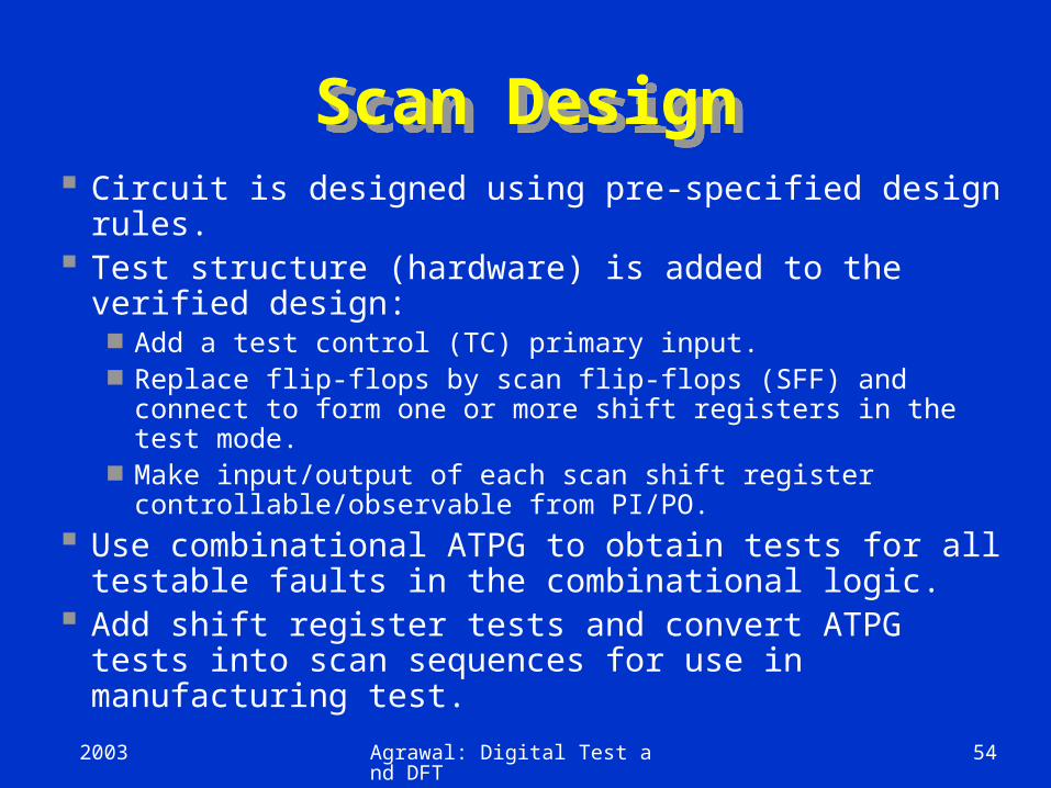
Scan DesignScan Design Circuit is designed using pre-specified design rules. Test structure (hardware) is added to the verified
design: Add a test control (TC) primary input. Replace flip-flops by scan flip-flops (SFF) and connect to
form one or more shift registers in the test mode. Make input/output of each scan shift register
controllable/observable from PI/PO. Use combinational ATPG to obtain tests for all
testable faults in the combinational logic. Add shift register tests and convert ATPG tests into
scan sequences for use in manufacturing test.
2003 Agrawal: Digital Test and DFT 55
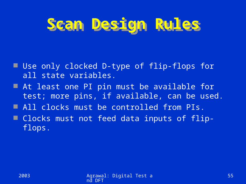
Scan Design RulesScan Design Rules
Use only clocked D-type of flip-flops for all state variables.
At least one PI pin must be available for test; more pins, if available, can be used.
All clocks must be controlled from PIs. Clocks must not feed data inputs of flip-flops.
2003 Agrawal: Digital Test and DFT 56
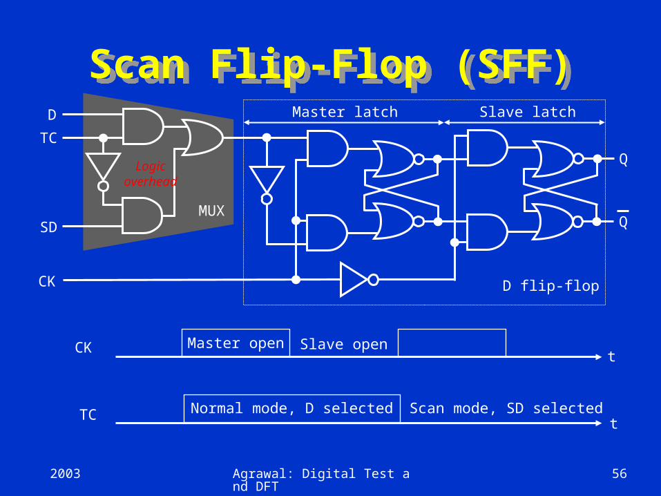
Scan Flip-Flop (SFF)Scan Flip-Flop (SFF)D
TC
SD
CK
Q
QMUX
D flip-flop
Master latch Slave latch
CK
TC Normal mode, D selected Scan mode, SD selected
Master open Slave opent
t
Logicoverhead

2003 Agrawal: Digital Test and DFT 57
Level-Sensitive Scan-Design Flip-Flop (LSSD-SFF)
Level-Sensitive Scan-Design Flip-Flop (LSSD-SFF)
D
SD
MCK
Q
Q
D flip-flop
Master latch Slave latch
t
SCK
TCK
SCK
MCK
TCK Norm
al
mode
MCK
TCK Sca
nm
ode
Logic
overhead

2003 Agrawal: Digital Test and DFT 58
Adding Scan StructureAdding Scan Structure
SFF
SFF
SFF
Combinational
logic
PI PO
SCANOUT
SCANINTC or TCK Not shown: CK or
MCK/SCK feed allSFFs.
2003 Agrawal: Digital Test and DFT 59
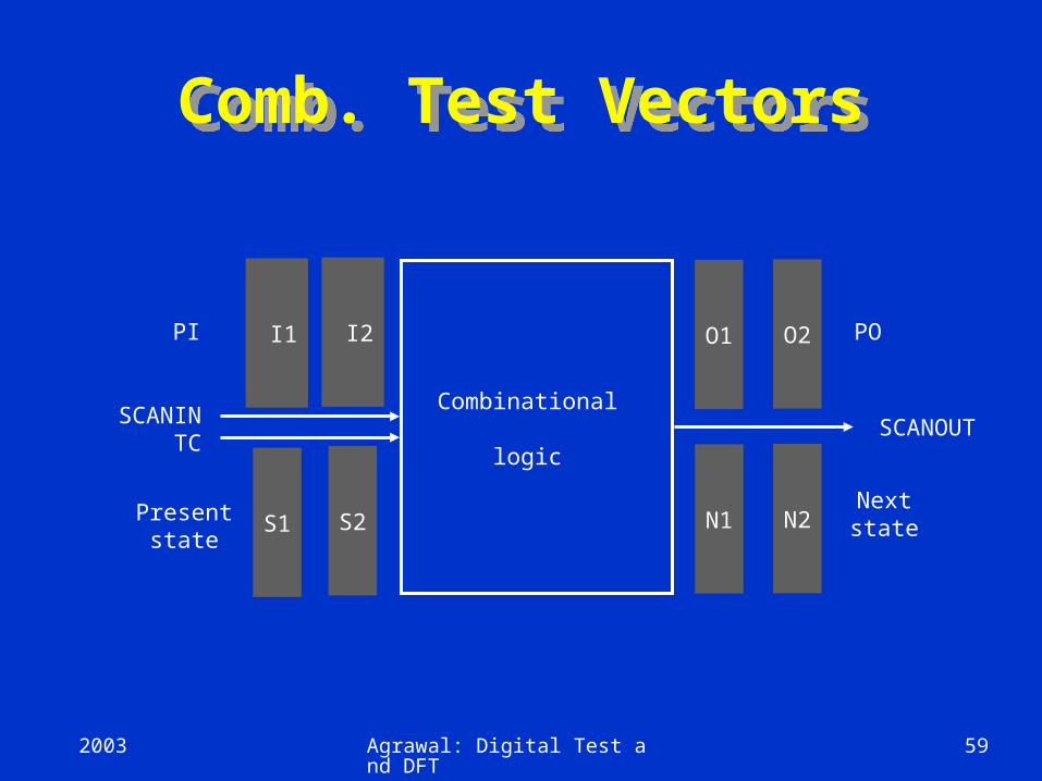
Comb. Test VectorsComb. Test Vectors
I2 I1 O1 O2
S2S1 N2N1
Combinational
logic
PI
Presentstate
PO
Nextstate
SCANINTC
SCANOUT

2003 Agrawal: Digital Test and DFT 60
Testing Scan RegisterTesting Scan Register Scan register must be tested prior to
application of scan test sequences. A shift sequence 00110011 . . . of length nsff+4
in scan mode (TC=0) produces 00, 01, 11 and 10 transitions in all flip-flops and observes the result at SCANOUT output.
Total scan test length: (ncomb + 2) nsff + ncomb + 4 clock periods.
Example: 2,000 scan flip-flops, 500 comb. vectors, total scan test length ~ 106 clocks.
Multiple scan registers reduce test length.

2003 Agrawal: Digital Test and DFT 61
Scan OverheadsScan Overheads IO pins: One pin necessary. Area overhead:
Gate overhead = [4 nsff/(ng+10nff)] x 100%, where ng = comb. gates; nff = flip-flops; Example – ng = 100k gates, nff = 2k flip-flops, overhead = 6.7%.
More accurate estimate must consider scan wiring and layout area.
Performance overhead: Multiplexer delay added in combinational path;
approx. two gate-delays. Flip-flop output loading due to one additional
fanout; approx. 5-6%.
2003 Agrawal: Digital Test and DFT 62
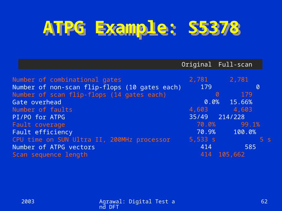
ATPG Example: S5378ATPG Example: S5378
Original
2,781 179 0 0.0% 4,603 35/49 70.0% 70.9% 5,533 s 414 414
Full-scan
2,781 0 179 15.66% 4,603214/228 99.1% 100.0% 5 s 585105,662
Number of combinational gatesNumber of non-scan flip-flops (10 gates each)Number of scan flip-flops (14 gates each)Gate overheadNumber of faultsPI/PO for ATPGFault coverageFault efficiencyCPU time on SUN Ultra II, 200MHz processorNumber of ATPG vectorsScan sequence length

2003 Agrawal: Digital Test and DFT 63
Summary: Scan DesignSummary: Scan Design Scan is the most popular DFT technique:
Rule-based design Automated DFT hardware insertion Combinational ATPG
Advantages: Design automation High fault coverage; helpful in diagnosis Hierarchical – scan-testable modules are easily
combined into large scan-testable systems Moderate area (~10%) and speed (~5%) overheads
Disadvantages: Large test data volume and long test time Basically a slow speed (DC) test
2003 Agrawal: Digital Test and DFT 64
Built-In Self-Test(BIST)
Built-In Self-Test(BIST)

2003 Agrawal: Digital Test and DFT 65
BIST ProcessBIST Process
Test controller – Hardware that activates self-test simultaneously on all PCBs
Each board controller activates parallel chip BIST Diagnosis effective only if very high fault coverage

2003 Agrawal: Digital Test and DFT 66
Example External XOR LFSR
Example External XOR LFSR
Characteristic polynomial f (x) = 1 + x + x3
(read taps from right to left)

2003 Agrawal: Digital Test and DFT 67
DefinitionsDefinitions Aliasing – Due to information loss,
signatures of good and some bad machines match
Compaction – Drastically reduce # bits in original circuit response – lose information
Compression – Reduce # bits in original circuit response – no information loss – fully invertible (can get back original response)
Signature analysis – Compact good machine response into good machine signature. Actual signature generated during testing, and compared with good machine signature

2003 Agrawal: Digital Test and DFT 68
Example Modular LFSR Response Compacter
Example Modular LFSR Response Compacter
LFSR seed value is “00000”

2003 Agrawal: Digital Test and DFT 69
Multiple-Input Signature Register
(MISR)
Multiple-Input Signature Register
(MISR) Problem with ordinary LFSR response
compacter: Too much hardware if one of these is put
on each primary output (PO) Solution: MISR – compacts all outputs into
one LFSR Works because LFSR is linear – obeys
superposition principle Superimpose all responses in one LFSR –
final remainder is XOR sum of remainders of polynomial divisions of each PO by the characteristic polynomial

2003 Agrawal: Digital Test and DFT 70
Modular MISR ExampleModular MISR Example
2003 Agrawal: Digital Test and DFT 71
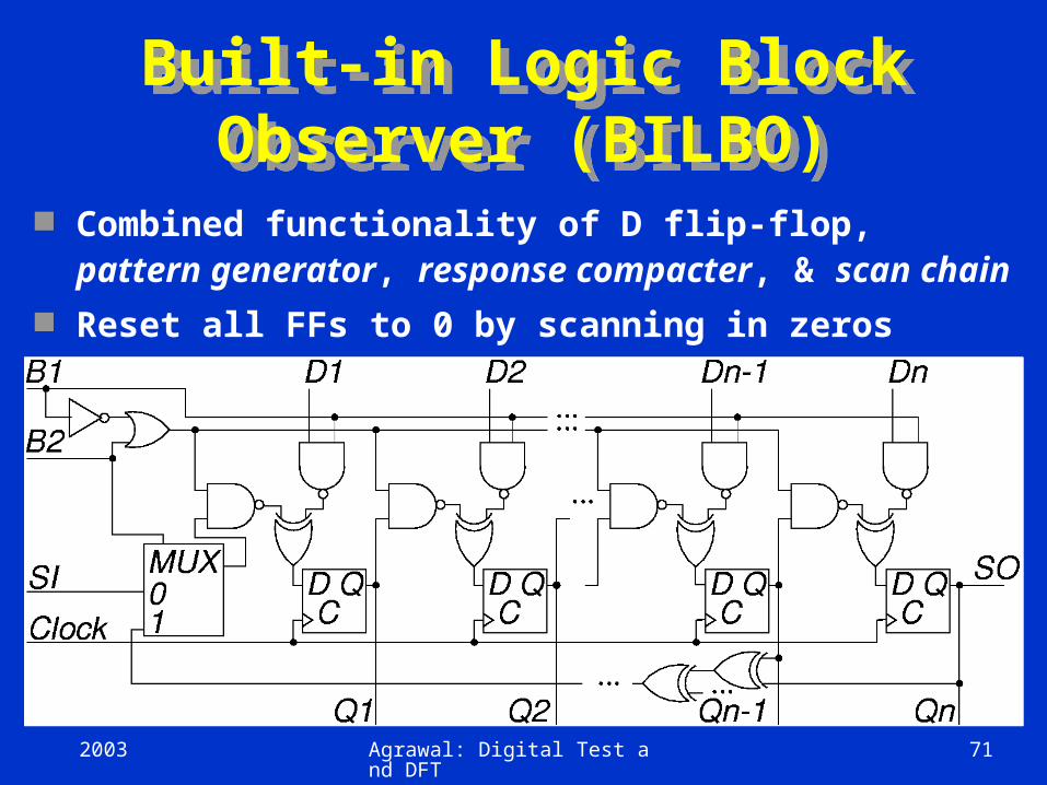
Built-in Logic Block Observer (BILBO)
Built-in Logic Block Observer (BILBO)
Combined functionality of D flip-flop, pattern generator, response compacter, & scan chain
Reset all FFs to 0 by scanning in zeros

2003 Agrawal: Digital Test and DFT 72
Circuit InitializationCircuit Initialization Full-scan BIST – shift in scan chain seed before
starting BIST Partial-scan BIST – critical to initialize all FFs before
BIST starts
Otherwise we clock X’s into MISR and signature is not unique and not repeatable
Discover initialization problems by:
1. Modeling all BIST hardware
2. Setting all FFs to X’s
3. Running logic simulation of CUT with BIST hardware

2003 Agrawal: Digital Test and DFT 73
Summary: BISTSummary: BIST LFSR pattern generator and MISR response
compacter – preferred BIST methods BIST has overheads: test controller, extra
circuit delay, Input MUX, pattern generator, response compacter, DFT to initialize circuit & test the test hardware
BIST benefits: At-speed testing for delay & stuck-at faults Drastic ATE cost reduction Field test capability Faster diagnosis during system test Less effort to design testing process Shorter test application times

2003 Agrawal: Digital Test and DFT 74
IEEE 1149.1 Boundary Scan Standard
IEEE 1149.1 Boundary Scan Standard

2003 Agrawal: Digital Test and DFT 75
System Test LogicSystem Test Logic

2003 Agrawal: Digital Test and DFT 76
Serial Board / MCM Scan
Serial Board / MCM Scan

2003 Agrawal: Digital Test and DFT 77
Parallel Board / MCM ScanParallel Board / MCM Scan

2003 Agrawal: Digital Test and DFT 78
Tap Controller SignalsTap Controller Signals Test Access Port (TAP) includes these signals:
Test Clock Input (TCK) -- Clock for test logic Can run at different rate from system
clock Test Mode Select (TMS) -- Switches system
from functional to test mode Test Data Input (TDI) -- Accepts serial test
data and instructions -- used to shift in vectors or one of many test instructions
Test Data Output (TDO) -- Serially shifts out test results captured in boundary scan chain (or device ID or other internal registers)
Test Reset (TRST) -- Optional asynchronous TAP controller reset

2003 Agrawal: Digital Test and DFT 79
Summary: Bound. ScanSummary: Bound. Scan Functional test: verify system hardware, software,
function and performance; pass/fail test with limited diagnosis; high (~100%) software coverage metrics; low (~70%) structural fault coverage.
Diagnostic test: High structural coverage; high diagnostic resolution; procedures use fault dictionary or diagnostic tree.
SOC design for testability: Partition SOC into blocks of logic, memory and analog
circuitry, often on architectural boundaries. Provide external or built-in tests for blocks. Provide test access via boundary scan and/or analog
test bus. Develop interconnect tests and system functional tests. Develop diagnostic procedures.
2003 Agrawal: Digital Test and DFT 80
IDDQ TestIDDQ Test

2003 Agrawal: Digital Test and DFT 81
Basic Principle of IDDQ Testing
Basic Principle of IDDQ Testing
Measure IDDQ current through Vss bus
2003 Agrawal: Digital Test and DFT 82
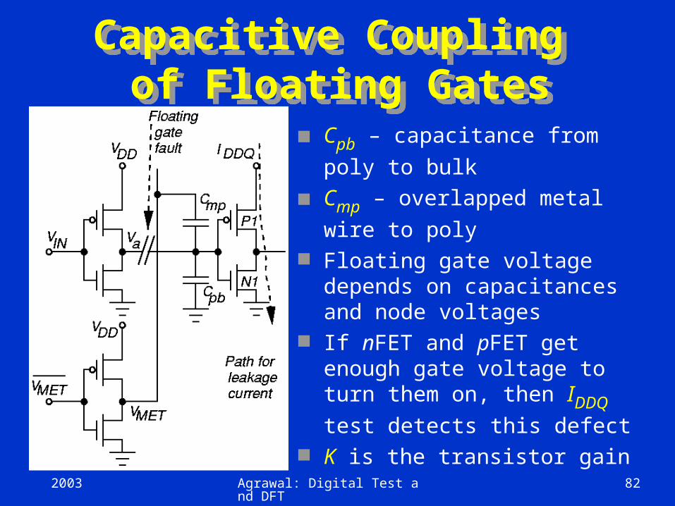
Capacitive Coupling of Floating Gates
Capacitive Coupling of Floating Gates
Cpb – capacitance from poly
to bulk Cmp – overlapped metal
wire to poly Floating gate voltage
depends on capacitances and node voltages
If nFET and pFET get enough gate voltage to turn them on, then IDDQ test
detects this defect K is the transistor gain

2003 Agrawal: Digital Test and DFT 83
Sematech ResultsSematech Results Test process: Wafer Test Package Test Burn-In & Retest Characterize & Failure
Analysis Data for devices failing some, but not all, tests.
passpassfailfail
pass
14652
pass
pass60136fail
fail14633413
1251pass
fail718
fail
passfail
passfail
Scan
-based
Stu
ck-a
t
IDDQ (5 A limit)
Functional
Scan
-based
dela
y
2003 Agrawal: Digital Test and DFT 84
Summary: IDDQ TestSummary: IDDQ Test IDDQ tests improve reliability, find defects
causing: Delay, bridging, weak faults Chips damaged by electro-static discharge
No natural breakpoint for current threshold Get continuous distribution – bimodal would be
better Conclusion: now need stuck-fault, IDDQ, and delay
fault testing combined Still uncertain whether IDDQ tests will remain
useful as chip feature sizes shrink further

2003 Agrawal: Digital Test and DFT 85
ReferencesReferences
M.L. Bushnell and V. D. Agrawal, Essentials of Electronic Testing for Digital, Memory and Mixed-Signal VLSI Circuits, Boston: Kluwer Academic Publishers, 2000, ISBN 0-7923-7991-8.
For the material on a course taught by the authors at Rutgers University, and a complete bibliography from the above book, see website:
http://cm.bell-labs.com/cm/cs/who/va