2009 midyear workshop f4-09: virtual architecture and design automation for partial reconfiguration...
TRANSCRIPT

2009 Midyear Workshop
F4-09: Virtual Architecture and F4-09: Virtual Architecture and Design Automation for Partial Design Automation for Partial ReconfigurationReconfiguration
All Hands Meeting
November 10th, 2009
Dr. Ann Gordon-RossAssistant Professor of ECE
University of Florida
Dr. Alan D. George Professor of ECE
University of Florida
Abelardo JaraTerence Frederick
Rohit KumarShaon Yousuf
Research StudentsUniversity of Florida

Outline Goals, Motivation and Challenges Virtual Architecture for Partially Reconfigurable Embedded System
(VAPRES) Design methodology Multiple clock domains support Bitstream relocation
MACS Inter-module Communication Architecture Case Study Application: Embedded Target Tracking System on
Virtex-4 FPGA board Preliminary non-PR version using Kalman filters
Design Automation for Partial Reconfiguration (DAPR) DAPR design flow
VHDL annotations Connectivity file and graph Device library file Overlay generation

3
GOAL – Leverage partial reconfiguration (PR) for application designers
Architect and implement a Virtual Architecture (VA) for Partially Reconfigurable
Embedded Systems
Ease PR design via design automation
MOTIVATIONS – Increase productivity and reduce
design complexity for PR designs VA reduces development time
Dynamically load and unload hardware processing modules
Processing hardware adapts to external environmental conditions
Automated design flow makes PR more amenable system designers Current PR design flow requires very high level of specialization Simplifies design of systems that time-multiplex FPGA resources → smaller devices
CHALLENGES Provide sufficient VA flexibility with architectural parameterization
Balancing enough application specialization with exploration complexity Creating new exploration algorithms/heuristics to automate PR design flow steps with
respect to available PR tools
33
Goals, Motivations, and Goals, Motivations, and ChallengesChallenges
Sensor Interface
Central Controlling Agent
ICAP Processed outputFilter repository
Filter A
Filter BPRR
Filter A
External Trigger
Sensor Coverage Area

44
Expand and prototype an FPGA-based architecture for rapid development of PR embedded systems VAPRES: Virtual Architecture for Partially
Reconfigurable Embedded Systems MACS: Minimal Adaptive Circuit Switching
mesh inter-module communication architecture for VAPRES Improvement over F4-08 SCORES
communication architecture Architectural support for hardware module
context save and restore Formulate and implement an
automated PR design flow DAPR: Design Automation for Partial
Reconfiguration Tool Study Virtex-4 and Virtex-5 bitstreams
to leverage additional functionalities Extend bitstream relocation and context
save and restore for Virtex-5
F4-09 ApproachF4-09 Approach
Highly specialized PR system design
Reconfiguration behavior known at design time
Highly optimized system floorplan based on known application
Flexible and reusable base architecture
Not optimized for a specific application
Tools to develop both reconfigurable modules and application software
DesignMethodology+ VAPRESBuilder Tool
VAPRES
Base Architecture

VAPRES: Architecture VAPRES: Architecture DesignDesign
Flexible scalable architecture Multiple architectural parameters enable
base system specialization N =number of PRRs kr =number of streaming channels going right kl =number of streaming channels going left Some additional parameters presented next
Base PR embedded system Multiple clock domains
PRMs can operate at independent clock frequencies
PRMs use FIFO-based I/O ports High speed inter-module
communication architecture (MACS)
Streaming channels
PRR1 PRR2 PRR3
FSL Interface
PLB Bus
MACS switch
ModuleInterfaces
ModuleInterfaces
ModuleInterfacescl
k1
clk2
clk0
ICAP
Flashcontroller
UART
SDRAMTo
ext
erna
l I/O
pin
s
Network
I/O
Mo
du
le
I/O
Mo
du
le
DCRBridge
ModuleInterfaces
ModuleInterfaces
MicroBlaze
PR S
ocke
t 1
PR S
ocke
t 2
PR S
ocke
t 3
Slice macros
To e
xter
nal I
/O p
ins
Control Region
Data Processing Region
kr=123
N= 123
kl=2
5

6
VAPRES: Design VAPRES: Design MethodologyMethodology
Applicationsoftware
PRMs
Application decompositionBase system
specifications
Software implementation
PRM design
Executable file Partial bitstreams Static bitstream
VAPRES API (vapres.h)
FPGA board
Base system design
Parametric VHDL
models
Synthesis
Application Flow(application designers)
Base System Flow(base system designer)
Implementation
System definition files
Synthesis
Implementation
Software implementatio
n
Software design
System designer chooses VAPRES
parameters
VAPRES VHDL, MHS,
MSS, and UCF
C/C++ libraries for application
software development
PRM implementation is separate from
base system implementation
Application designers
work separate from system
designerParametric models for
VAPRES and MACS enable customization
Floorplan
System floorplan
defines PRR sizes and shapes

7
VAPRES: Builder ToolVAPRES: Builder Tool Overview
Automates process of buildingVAPRES base system and applications Increases designers productivity
Builder Tool Features Some additional parameters used
PRR height and width Automatic creation of VAPRES base
system from parameters Base system floorplanning Slice macro instantiation and
placement Automatic implementation of static
and partial bitstreams Assisted framework for application
designers Generates VAPRES SW libraries Templates for PRMs and software
Static base system
PR modules (PRMs)
Application software
Architectural parameters
Systemfloorplan
(.ucf)
Top VHDL entity (.vhd)
Software specifications
(.mss)
Hardware specifications
(.mhs)

Design 1 Design 2 Design 3 Design 4
Number of PRRs 1 1 2 3
PRR height 1 row (16 CLBs) 2 rows (32 CLBSs) 2 rows (32 CLBs) 1 row (16 CLBs)
PRR width 10 CLBs 10 CLBs 10 CLBs 10 CLBs
MACS parameters N=1, kr=1, kl=1 N=1, kr=1,kl=1 N=2, kr=2,kl=2 N=3, kr=2,kl=2
Post-place and route implementation for base static system
Maximum clock 120.3 MHz 117.6 MHz 116.1 MHz 119.3 MHz
Static region slices (without MACS)
6927 6927 7211 7474
MACS slices N/A N/A 928 2745
8
VAPRES Builder – ResultsVAPRES Builder – Results
N = number of PRRs = number of MACS switches, kr = number of channels between switches going in the right direction, kl = number of channels between switches going in the left direction
Set of slice macros (1 set for each PRR)
PRR boundary
1 1 2 3
≈ 280 slices more when when adding
an extra PRR
+0 slices +284 slices +263 slices
100 MHz constraint met for all place-
and-routed designs

Only one partial bitstream necessary for each PRM Partial bitstreams stored in compact flash When PRM is needed, partial bitstream is loaded into Microblaze and relocator is called New partial bitstream is loaded into correct PRR
Program runs in external memory: Bitstream relocator is stored in non-volatile compact flash System ACE controller loads relocator from flash and stores it in SDRAM
Microblaze
PRR1 PRR2
FS
L Interf,
PLB Bus
InterfaceInterface
I/O
Mod
ule
Interface Interface
clk0
clk1
ICAP
SystemACEFlash
UART
SDRAM
To
exte
rnal
I/O
pin
s
To
exte
rnal
I/O
pin
s
Network
9
VAPRES – Bitstream VAPRES – Bitstream Relocation Relocation
SCORES Switch
Data Processing Region (includes one or more RSBs – Reconfigurable Streaming Blocks)System Control Region
In-situ Bitstream Relocation – Alters partial bitstream (with no external inputs) to run in any PRR Advantages:
Reduces bitstream storage requirements (only one partial bitstream per module) Saves step of reading a partial bitstream from external Flash memory, if similar
partial bitstream was already loaded into memory Enables VAPRES to dynamically place and migrate modules
Restriction – PRRs must be homogeneous (ensures sufficient resources)
I/O
Mod
ule

Overview – MACS Communication Overview – MACS Communication ArchitectureArchitecture
10
MACS: Minimal adaptive circuit switching mesh communication architecture VAPRES requires high-bandwidth, low-latency communication
channels inside reconfigurable streaming blocks (RSBs) Novel communication architecture named SCORES was
implemented in 2008 MACS extends SCORES from linear array topology to mesh
topology with few other new features
Features of MACS Minimal-adaptive routing to explore all possible shortest paths
Selects lowest cost path that best achieves network load distribution Similar interface ports for nodes and neighboring switch
Any number (<=6) of nodes can be put on a single switch Unused interface ports, of switches around edges of NoC, can be
utilized Node interface port available in MxN NoC is <= 2(M*N + M + N) Reduces area overhead of communication architecture per node
Provides low-latency path(s) between frequently communicating node pairs (if attached to same switch)
10
S
NN
S
NN
S
NN
S
NN
S
NN
S
NN
S
NN
S
NN
S
NN
MACS

11
MACS implementation results (1/2) 9 architectural parameters to play around with
Plotting all combinations is not feasible Assuming two values of each parameter requires 29 “area usage” plots and
29 “achievable frequency” plots
Figure 1: Area usage in number of slices per module for data widths W = 8, 16, and 32 bits for a varying number of lanes per switch and local port. The x-axis in each graph varies the Kl, Kr, Kd, and Ku parameters from 1 to 3 lanes per switch port. Left to right, the graphs vary the Kll and Krl parameters from 1 to 3 lanes per local port.
Figure 2: Maximum operating frequency for data widths W = 8, 16, and 32 bits for a varying number of lanes per switch and local port. The x-axis in each graph varies the Kl, Kr, Kd, and Ku parameters from 1 to 3 lanes per switch port. From left to right, the graphs vary the Kll and Krl parameters from 1 to 3 lanes per local port.
12
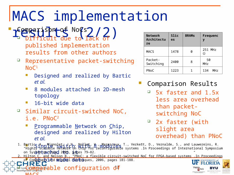
MACS implementation results (2/2) Comparison of NoCs
Difficult due to lack of published implementation results from other authors
Representative packet-switching NoC1
Designed and realized by Bartic et al. 8 modules attached in 2D-mesh topology 16-bit wide data
Similar circuit-switched NoC, i.e. PNoC2
Programmable Network on Chip, designed and realized by Hilton et al.
Single switch with 8 modules attached to it 16-bit wide data
Comparable configuration of MACS 2x2 mesh of MACS switches W=16, Ku=Kd=Kl=Kr=Kil=Kir=1
Network Architecture
Slices BRAMs Frequency
MACS 1478 0 251 MHz
Packet-Switching
2400 8 50 MHz
PNoC 1223 1 134 MHz
Comparison Results 5x faster and 1.5x less area
overhead than packet-switching NoC
2x faster (with slight area overhead) than PNoC
1. Bartic, A., Mignolet, J.Y., Nollet, V., Marescaux, T., Verkest, D., Vernalde, S., and Lauwereins, R. “Highly scalable network on chip for reconfigurable systems”.In Proceedings of International Symposium on System-on-Chip, 2003, pages 79–82.
2. Hilton C. and Nelson B., “PNoC: a flexible circuit-switched NoC for FPGA-based systems”.In Proceedings of Computers and Digital Techniques, 2006, pages 181-188.

Analytical model of SCORES/MACS Streaming network
FIFO at both ends: Producer FIFO (of size D), Consumer FIFO (of size C)
Pipelined channel/medium: n-stage pipeline
Control Feedback Path n-stage
Phases I Analysis of producer-medium and medium-consumer pairs
Phase II Analysis of medium-consumer with feedback
Analytical ModelingAnalytical Modeling
13
λp λm λm
n-stage
n-stage
Size D Size C
µm µc

Markov-chain modelPhase-I: Producer-Medium Phase-I: Producer-Medium Pair(1/2)Pair(1/2)
14
λp μm
Size D
1 2 k
λp,1λp,k-1 λp,k
μm,k+1μm,kμm,2
D
λp,D-1
μm,D
k+1
• Pk probability associated with the queue being in state k i.e. queue having k packets in it• λp = Arrival rate• μm = Service rate• D = System capacity• Flow = Sum of product of λ’s, μ’s and P’s
Solving for steady state gives
0
λp
μm,1
1,
,
0
1
0
1
km
kpkk
k
kand
P
P
P
P
kkmkpkkmkkp
kPPP
dt
dP*)(** ,,11,11,
0dt
dPk
1,
,1,11, **
km
kp
k
kkkpkkm P
PPP
002
201 *...,*,* PPPPPP kk
P0 P1 P2 Pk Pk+1 PD

Phase-I: Producer-Medium Phase-I: Producer-Medium Pair(2/2)Pair(2/2)
15
m
p
DD
DP
1 for )1(
)1(1
PD
1/(D+1)
D (line size)
D
1
1
1
1for 1
1
1)...1(
0
20
DP
DP
P
D
D
Total probability of the system should be 1
10
D
k
kP
)1(
)1(
)1(
)1()...1(
1
10
20
0
DD
D
DD
D
k
P
PPP

Phase II: Medium-Consumer Pair Phase II: Medium-Consumer Pair with control feedback, 2D-Markov with control feedback, 2D-Markov Chain Model (1/2)Chain Model (1/2)
16
Streaming network Number of packets in queue(k) Recently reached threshold(Q)
Potential Queuing at Q = 0 Producer is filling with rate λp
Service rate is µm
At k = D-1, queue
switches to de-queuing state Potential De-queuing at Q = 1
Producer is filling with reduced
rate λp,1
Consumer is emptying with µm
Total probability of state Q = 1 gives the Packet drop probability At k = 1, queue switches to queuing state, i.e. Q=0
PD,1
1 2 k
λp λp λp
µmµmµm
λp
D-10
λp
µm
P0 P1 P2 Pk Pd-1
1 2 i
λp,1 λp,1 λp,1
µmµmµm
D
λp,1
µm
D-1P1,1 P2,1 Pi,1 Pd-1,1
Q=1
Q=0
k
µm
λp,1 µm
λp

Probability of FIFO being filled with ‘k’ packets when ρ ≠ 1
Probability of FIFO being filled with ‘k’ packets when ρ = 1
17
Phase II: Medium-Consumer Pair with control feedback, 2D-Markov Chain Model (2/2)
Packet Drop Probability when ρ ≠ 1
Packet Drop Probability when ρ = 1
0 and where
11
1
p,1p
1
D
Ddrop
D
DP
drop
kD
k PD
P
1
1
3
1
D
Pdrop
3
DD
kDPk

18
Real-time Simulation and Profiling Real-time Simulation and Profiling of MACSof MACS Setup for basic experiment
One MACS switch with both module interface occupied Network frequency = Module frequency = 100 MHz Producer and consumer rates are Poisson process ROM holds MATLAB generated Poisson distributed intervals
based on different λ and µ Producer/consumer loads its counter with value from ROM and
generates/reads a unit of data at counter overflow ChipScope ILA core captures all FIFO activity System parameters: FIFO sizes = 512 bytes, Network
BW = 400MBps, Producer rate = 40MBps Consumer Rate = 4MBps, (both generates data at Poisson distributed random intervals), Transfer size = 0-128KB
Results Link utilization = 1/10.35, before consumer FIFO is full (at
transfer size ~46KB) Link utilization = 1/105.8081, after consumer FIFO is full
(at transfer size > 46KB) Both FIFO’s activity and probability distribution of
consumer FIFO being ‘almost’ full is also plotted w.r.t to transfer size
S
NN
S
NNS
NN
S
NN
S
NN
S
NN
S
NN
S
NN
S
NN

19
Setup for advanced experiment 3x3 MACS NoC with both module interface occupied for each switch Network frequency = Module frequency = 100 MHz Producer and consumer rates are linear ChipScope ILA core captures all activities such as request establishment,
write enables for FIFO (used in link utilization calculation), average number of retrials for establishing a channel, avg. channel establishment latency, etc
Observe aforementioned parameters for various network traffic patterns Network traffic generation patterns
Real-time Simulation and Profiling of MACSReal-time Simulation and Profiling of MACS
Pattern Name Description
Uniform Random Module chooses a random destination among all the other modules and sends a packet to that destination. The probability is equal among the other modules
Nearest Neighbor
Each node send a packet to a module of its immediate neighbor switch with equal probability
Tornado {X, Y} will send packets to destination {X+k/2−1, y} mod k for the k-ary network (k=4)
Transpose Router of the address {X, Y} will send a packet to router {Y, X}
Bit Complement Node with address {b0,b1,b2,b3} in bits will send packets to the destination address NOT{b0,b1,b2,b3} in bits
Hot Spot All the nodes send the packet to a certain node. Hot spot can act as receiver only or can be both transmitter and receiver.

HDL Synthesis
Implement Base Design
Implement PR Modules
Merge
Timing/Placement Analysis
Manual Steps
Automated Steps
DAPR Tool
Overview - Design Automation for Partial Reconfiguration (DAPR) Xilinx Early Access (EA) PR Flow provides PR system design support
Existing PR flow is very specialized Requires target device architecture knowledge System designer must manually apply steps
Hierarchical coding of HDL design description, synthesis, floorplanning, timing analysis implementation and merge
DAPR design flow will mitigate existing PR design flow intricacies Manual Steps
Hierarchical HDL design description Modified HDL design description via system designer annotations System designer annotated design constraints (optional)
Automated Steps DAPR inputs - modified HDL design description and design constraints (parameters include bitstream size, timing, power) DAPR design exploration - iteratively generates candidate
design and compares generated design performance parameters with system designer annotated constraints
DAPR output – Final bitstreams if system designer constraints are met otherwise output final bitstreams that match closest to system designer annotated constraints
HDL Design Description
Final Generated Bitstreams
Merge
Modified HDL
Design Description
Design Constraints(optional)
DAPR Design FlowDAPR Design Flow
EA PR FlowEA PR Flow
20
HDL Design Description
HDL Synthesis
Set Design Constraints
Implement Base Design
Implement PR Modules
Timing/Place-ment
Analysis

Overview - DAPR Tool Phases and Description
21
Initial input
Modified VHDL
Top File
Phase 1Information Extraction
Phase 2Information Collection
Run script to synthesize modules and estimate resource requirements
Phase 3Overlay
Generation
Implement and merge design
Perform automated floorplanning and write to User Constraint File (UCF)
VHDL Top File
PR automation information File (.paif)
Generated full and partial bitstreams
PRRs identification
Static region identification
Device inf.libraries(.dilf)
DAPR tool starts here
Phase 4Bitstream Generation
Information Extraction Extract static and PR region instantiations and
corresponding HDL design description filenames from top level HDL design description file
Information Collection Collect and write port connection names and widths
within each instantiation to partial reconfiguration automation information file (*.paif)
Resource Estimation and Constraint Generation Synthesize all HDL design description file
with Xilinx XST utility Read and record estimated slice requirements
from generated synthesis log file (.srp) to .paif Generate connectivity information and
PRR floorplan using estimated resources and device information libraries
Bitstream Generation Implement static region and PRMs with Xilinx’s
ngdbuild, MAP, and PAR utilities Merge top, static, and PRMs with Xilinx’s PR_verify
design and PR_assemble utilities to generate final full and partial bitstreams

A simple example design with two PRRs Two 32-bit up and down counter modules
map to PRR 1 Two 8-bit up and down counter modules
map to PRR 2 Connectivity information gathered from .paif
file and connectivity graph generated for system designer verification
Example system designer annotations (Case
insensitive)--PRR_Start :: filename, filename… --Static_Start :: filename, filename… --bm_start --PRR_clock
Significance of system designer annotation
Identifies beginning PRR instantiation and PRM filenames (use comma to
specify multiple filenames)
Identifies static region instantiation and filenames (use comma to specify multiple
filenames)
Identifies slice Macro instantiation
Identifies system top level clock
System Designer Annotations and Connectivity Information Examples
---------------------------------------------------PRR_start :: prm_up, prm_down
reconfig : rmodule Port Map(
led_in=> rm_in_int,led_out=> rm_out_int);
-------------------------------------------------
---------------------------------------static_start:: static
led_registers : base Port Map( clk=> clk,
led_unreg=> rm_out,led_reg=> rm_in);
-------------------------------------
----------------------------------------------------------bm_start
in0 : busmacro_xc4v_l2r_sync_narrowPort Map(input0 => bml2r(0), input1 => bml2r(1),input2 => bml2r(2),
--------------------------------------------------------
Connectivity Information Example 32
Design Connectivity Graph
Counter
Static Region32
8 Counter_sm
8
Module Name/Type
Incoming Connections
Outgoing Connections
Base/Static 40 40
Counter/PR 32 32
Counter_sm/PR 8 8
Design Connectivity Information Table

DAPR V4LX25 Device Library
Bank 0 Bank 2 Bank 1
Device divided into 3 banks Bank 0 (left), Bank 1(right),
Bank 2(center) Resource representation
Single letter with prefix of either 1 or 0 Letters are S for Slices, D for
DSP48s, F for FIFO16s, R for RAMB16s, C for DCM’s, G for BUGF’s
Prefix of 0 means resource occupied, 1 means resource vacant
Checking individual values will help identify resource type and also resource availability
Device Library file will be shown in Demo

DAPR Overlay Generation Overlay generation uses Cluster growth algorithm Cluster Growth Algorithm works in two steps Linear ordering of modules
Choose seed module from initial set of modules and move to a new set of ordered modules (initially an empty set)
Compute gain for each remaining module (gain is number of connecting nets)
Move module with highest gain to set of ordered modules and repeat from gain computation until no more modules are remaining in the initial set
Place ordered modules on floorplan space Two types of floorplan growth – Vertical and Diagonal Current overlay generator floorplans builds vertically
Advantage - bitstream size will be smaller Disadvantage - routing is difficult and will take longer
Floorplan Growth DirectionFloorplan Growth Direction
Floorplan Growths (diagonal (left) and veritcal (right) and colored blocks represent PRMs)
1 CLB wide and 16 CLB tall
25
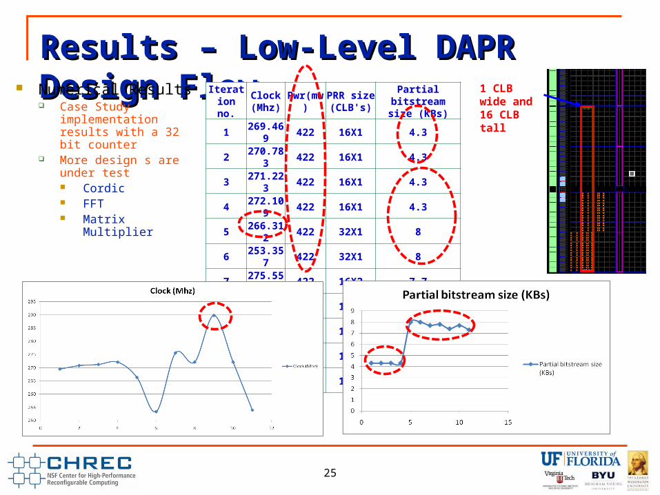
Results – Low-Level DAPR Results – Low-Level DAPR Design FlowDesign Flow Numerical Results Case Study
implementation results with a 32 bit counter
More design s are under test Cordic FFT Matrix Multiplier
Iteration no.
Clock (Mhz) Pwr(mw) PRR size
(CLB's)Partial bitstream
size (KBs)1 269.469 422 16X1 4.32 270.783 422 16X1 4.33 271.223 422 16X1 4.34 272.109 422 16X1 4.35 266.312 422 32X1 86 253.357 422 32X1 87 275.558 422 16X2 7.78 272.109 422 16X2 7.89 289.771 422 16X2 7.4
10 272.109 422 16X2 7.711 253.936 422 16X2 7.3
1 CLB wide and 16 CLB tall

Data format For the X and Y coordinates
16 bits fixed point representation: 1 sign bit; 8 integral bits and 7
fractional bits For the 2 FIFOs
Implemented using one Virtex-4 BRAM
Each one has 32 bits width (16 for X and 16 for Y) and 512 words
depth
The process of the system
2626
Kalman Filter Case Study
26

Application Target tracking in linear system:
Provide accurate, continuously updated information about the position of a target given a
sequence of observations about its position.
Dynamic model and measurement model are linear
Noises are Gaussian distributed
The system model:
The dynamic system model:
Uniform velocity motion:
The measurement model:
2727
Kalman filter - Introduction
27
1 Wk k k k x F x
[ , , , ]k k k xk ykx y v vx W (0, )k kN Q
k k k k z H x v
1 0 0
0 1 0
0 0 1 0
0 0 0 1
k
T
T
F
1 0 0 0
0 1 0 0kH
(0, )k kNv R

Initialization
Predict Predicted state:
Predicted covariance :
Update Innovation measurement :
Innovation covariance:
Optimal Kalman gain:
Update state estimate:
Update estimate covariance:
The simplified version – Fixed-gain Kalman filter Difference
The optimal Kalman gain is acquired before processing and keep fixed .
Application If the system is stationary stochastic process, the Kalman gain does not change.
2828
Kalman filter algorithm
28
| 1 1| 1ˆ k k k k k x F x
| 1 1| 1 1T
k k k k k k k P F P F Q
| 1ˆk k k k k y z H x
| 1T
k k k k k k S H P H R1
| 1T
k k k k k
K P H S
| | 1ˆ ˆk k k k k k x x K y
| | 1k k k k k kI P K H P
0|0x 0|0P

8 multiplications Read and write FIFOs for Kalman filter part
The process control If the FIFO TX is Full, stop writing and reading the data from the FIFO RX.
-> stop processing data
The time interval guarantee At least 3 clock cycles
Parameters input Parameters (fixed Kalman gain, initial values) are inputted instead of being pre-
programmed in the system
2929
Type 1: Fixed-gain Kalman filter
29

For the flexibility of application, use 8 DSP to Instantiate the multipliers
Resources consumption (V4LX25)
Number of Slices: 280 (2%) Number of DSP48s: 8 (16%)
Maximum frequency 156.2 MHz, Throughput 52 MSPS (3 cycles)
Dynamic power consumption (100MHz CLK) 0.06118 W
Estimated results comparison
Bouncing ball experiment
Fixed-gain Kalman filter is suitable
Results calculated by FPGA are
identical to Matlab
3030
Results & Analysis
30

3131
Type 2: Basic version of Kalman filter
31
Assuming all noises are non-coherent, four elements in Kalman gain matrix are zero.
4 divisions and 12 multiplications.

Reduce number of dividers and multipliers by resources reuse
Estimated results comparison
Bouncing ball experiment
Kalman filter gain updates in each
iteration
Results calculated by FPGA
are identical to Matlab
3232
Results & Analysis
32
4 divs & 12muls 2 divs & 6muls 1 div & 3muls
Slices (V4LX25) 1958 (18%) 1316 (12%) 1033 (9%)
DSP48s 12 (25%) 6 (12%) 3 (6%)
Max. frequency 71.4 MHz 71.4 MHz 71.4 MHz
Processing time 23 clock cycles 24 clock cycles 26 clock cycles
Throughput 3.1 MSPS 2.9 MSPS 2.7 MSPS
Dynamic power (50MHz CLK) 0.09970 W 0.07556 W 0.08092 W