200v epc2112 egan® hemt - system plus consulting€¦ · company profile & supply chain...
TRANSCRIPT

1©2019 by System Plus Consulting | 200V EPC2112 eGaN® HEMT with Monolithic Optimized Gate Driver | Sample
200V EPC2112 eGaN® HEMT with Monolithic Optimized Gate DriverSP19415 - Power Semiconductor report by Amine ALLOUCHE
Laboratory Analysis by Nicolas RADUFESeptember 2019 – SAMPLE
+33 2 40 18 09 16 [email protected] www.systemplus.fr22 Bd Benoni Goullin
44200 NANTES - FRANCE
REVERSE COSTING® – STRUCTURAL, PROCESS & COST REPORT

2©2019 by System Plus Consulting | 200V EPC2112 eGaN® HEMT with Monolithic Optimized Gate Driver | Sample
Table of Contents
Overview / Introduction 4
o Executive Summary
o Market
o Reverse Costing Methodology
o Glossary
Company Profile & Supply Chain 11
o EPC Profile
o EPC GaN Products
Physical Analysis 17
o Methodology
o Summary of the Physical Analysis
o Package Analysis
Package Opening
Package Cross-Section
o Die: IC Gate Driver
Die View & Dimensions
Die Cross-Section
Die Process
Die Process Characteristics
o Die: eGaN® FET
Die View & Dimensions
Die Cross-Section
Die Process
Die Process Characteristics
Manufacturing Process Flow 54
o Die Front-End Fabrication Unit
o Die Front-End Process Flow
o Final Test & Packaging Fabrication Unit
o Die Back-End Process Flow
Cost Analysis 63
o Summary of the cost analysis
o Yields Explanation & Hypotheses
o Device Cost
Wafer Front-End Cost
Wafer Front-End Cost per Step
Packaging Cost
Die Cost
Die Back-End (Probe Test and Dicing) Cost
Component Cost
Price Analysis 74
o Definition of Prices
o Estimation of selling price
Comparison 77
o Comparison between Integrated drivers GaN FET from EPC and Navitas
o Comparison between 200V EPC eGaN® FETs
Feedbacks 80
Company services 82
3©2019 by System Plus Consulting | 200V EPC2112 eGaN® HEMT with Monolithic Optimized Gate Driver | Sample
Overview / Introductiono Executive Summaryo Marketo Reverse Costing
Methodologyo Glossary
Company Profile & Supply Chain
Physical Analysis
Manufacturing Process Flow
Cost Analysis
Selling Price Analysis
Comparison
Related reports
About System Plus
Executive Summary
System Plus Consulting proposes a complete reverse costing of the EPC2112, the first monolithically integrated HEMTfrom Efficient Power Conversion (EPC). The device is an enhancement-mode gallium-nitride (eGaN®) single FieldEffect Transistor (FET) with a Gate Driver Integrated Circuit (IC). It is adapted for High Frequency DC-DC conversionand Wireless Power applications.
This new Integrated Gate Driver eGaN® IC design consists of a 40-mΩ, 200V eGaN® power transistor and anoptimized gate driver in a low inductance surface mount Ball Grid Array (BGA) package.
Compared with their silicon counterparts, GaN transistors have significantly lowered capacitance. This translates intolowered switching losses at higher frequencies for the same on-resistance and voltage rating. Besides this, EPC’s chip-scale packaging significantly reduces its final device costs, bringing a competitive advantage not only withcompetitors in GaN but also with silicon.
Based on a complete teardown analysis, this report provides a detailed manufacturing cost analysis of the die and thepackage as well as the estimated selling price of the device. Moreover, the report includes a technology and costcomparison of this unique EPC2112 device with the monolithic GaN solution proposed by Navitas. Finally, this reportprovides a comparison of EPC2112 with the previous 200V EPC GaN device, the EPC2010. This comparison highlightsthe differences in die design and their impact on production cost.
4©2019 by System Plus Consulting | 200V EPC2112 eGaN® HEMT with Monolithic Optimized Gate Driver | Sample
Overview / Introduction
Company Profile & Supply Chain o EPC Profileo EPC GaN Products
Physical Analysis
Manufacturing Process Flow
Cost Analysis
Selling Price Analysis
Comparison
Related reports
About System Plus
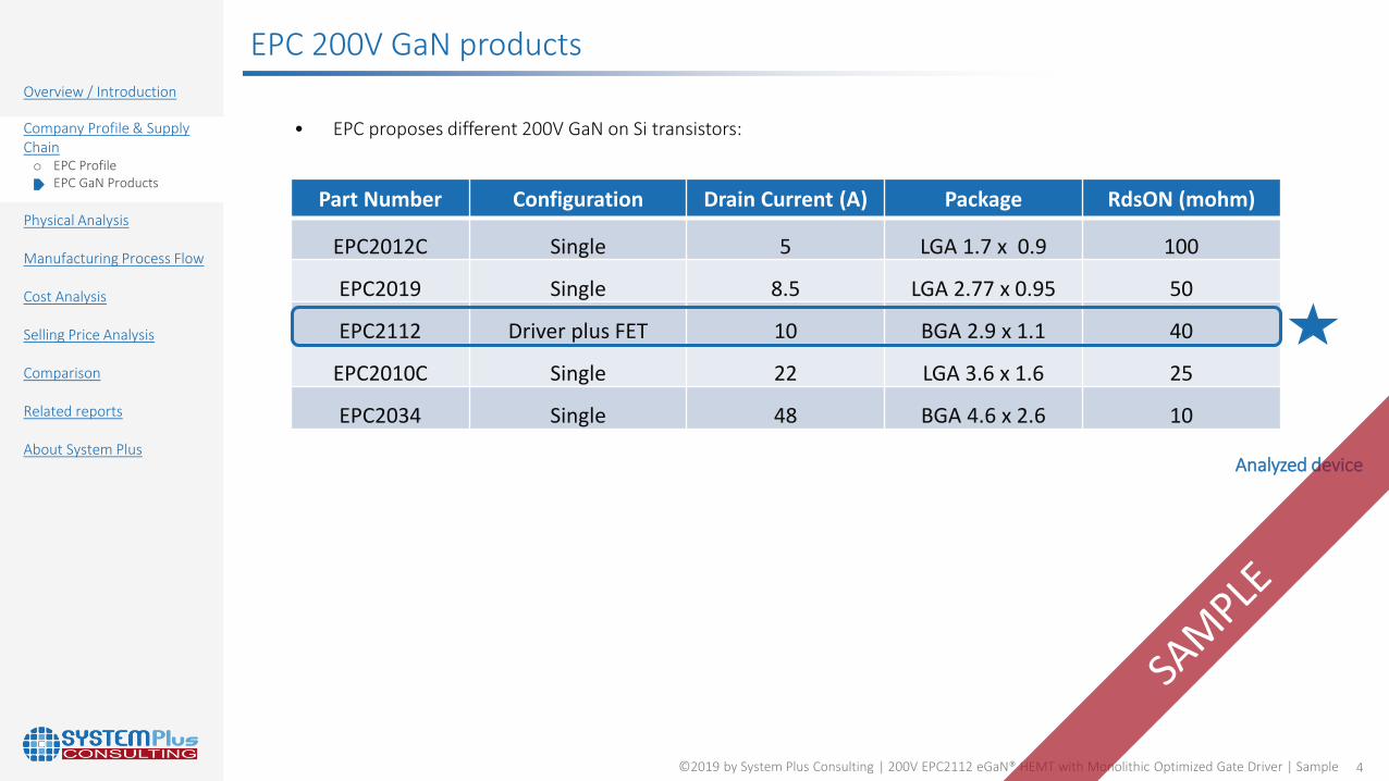
Part Number Configuration Drain Current (A) Package RdsON (mohm)
EPC2012C Single 5 LGA 1.7 x 0.9 100
EPC2019 Single 8.5 LGA 2.77 x 0.95 50
EPC2112 Driver plus FET 10 BGA 2.9 x 1.1 40
EPC2010C Single 22 LGA 3.6 x 1.6 25
EPC2034 Single 48 BGA 4.6 x 2.6 10
EPC 200V GaN products
• EPC proposes different 200V GaN on Si transistors:
Analyzed device
5©2019 by System Plus Consulting | 200V EPC2112 eGaN® HEMT with Monolithic Optimized Gate Driver | Sample
Overview / Introduction
Company Profile & SupplyChain
Physical Analysis o Methodologyo Summaryo Packageo IC Gate Drivero eGaN® FET
Manufacturing Process Flow
Cost Analysis
Selling Price Analysis
Comparison
Related reports
About System Plus
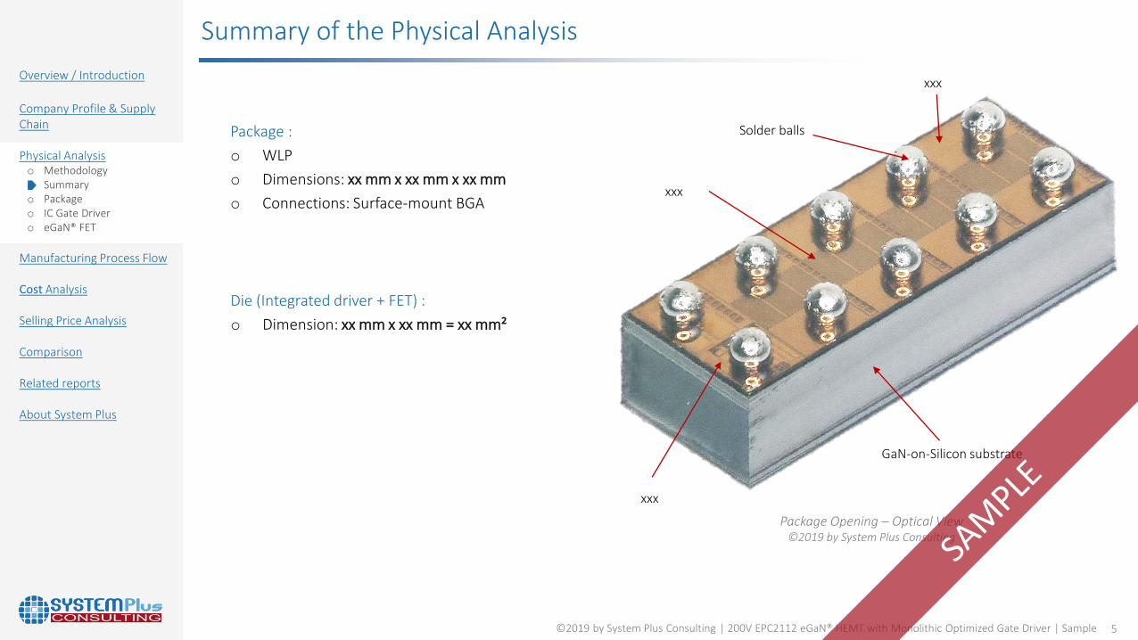
Summary of the Physical Analysis
Package :
o WLP
o Dimensions: xx mm x xx mm x xx mm
o Connections: Surface-mount BGA
Die (Integrated driver + FET) :
o Dimension: xx mm x xx mm = xx mm²
Solder balls
xxx
Package Opening – Optical View©2019 by System Plus Consulting
xxx
GaN-on-Silicon substrate
xxx
6©2019 by System Plus Consulting | 200V EPC2112 eGaN® HEMT with Monolithic Optimized Gate Driver | Sample
Overview / Introduction
Company Profile & SupplyChain
Physical Analysis o Methodologyo Summaryo Packageo IC Gate Drivero eGaN® FET
Manufacturing Process Flow
Cost Analysis
Selling Price Analysis
Comparison
Related reports
About System Plus
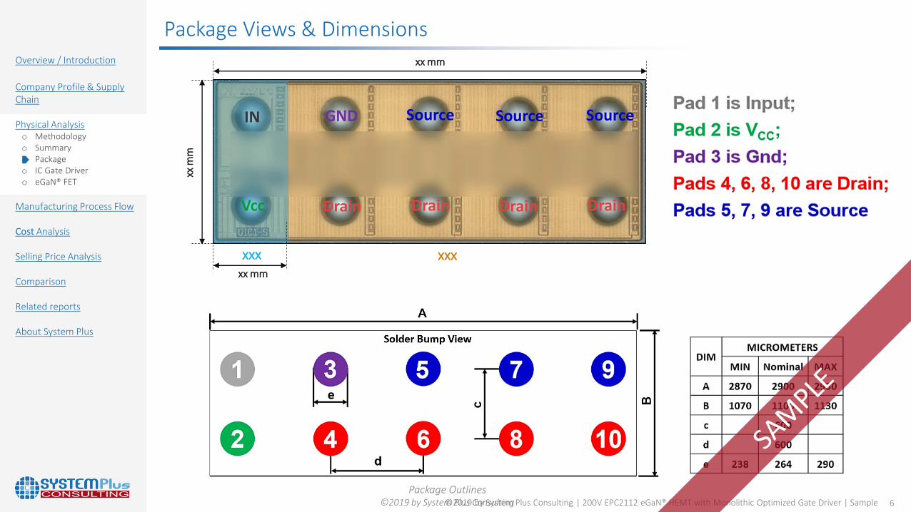
Package Views & Dimensions
Package Outlines©2019 by System Plus Consulting
Source Source Source
Drain Drain Drain
GND
Drainxx
mm
xx mm
IN
Vcc
xxx xxxxx mm
7©2019 by System Plus Consulting | 200V EPC2112 eGaN® HEMT with Monolithic Optimized Gate Driver | Sample
Overview / Introduction
Company Profile & SupplyChain
Physical Analysis o Methodologyo Summaryo Packageo IC Gate Drivero eGaN® FET
Manufacturing Process Flow
Cost Analysis
Selling Price Analysis
Comparison
Related reports
About System Plus
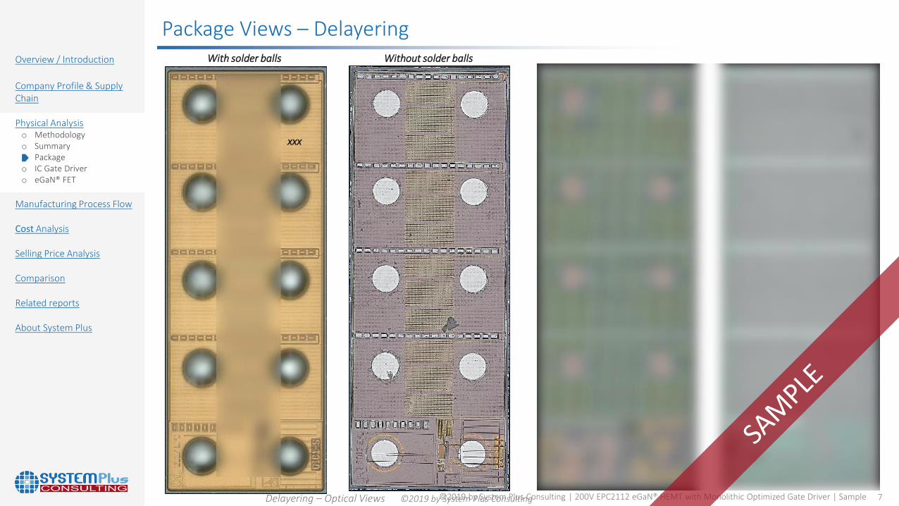
Package Views – Delayering With solder balls
xxx
Without solder balls
Delayering – Optical Views ©2019 by System Plus Consulting
8©2019 by System Plus Consulting | 200V EPC2112 eGaN® HEMT with Monolithic Optimized Gate Driver | Sample
Overview / Introduction
Company Profile & SupplyChain
Physical Analysis o Methodologyo Summaryo Packageo IC Gate Drivero eGaN® FET
Manufacturing Process Flow
Cost Analysis
Selling Price Analysis
Comparison
Related reports
About System Plus
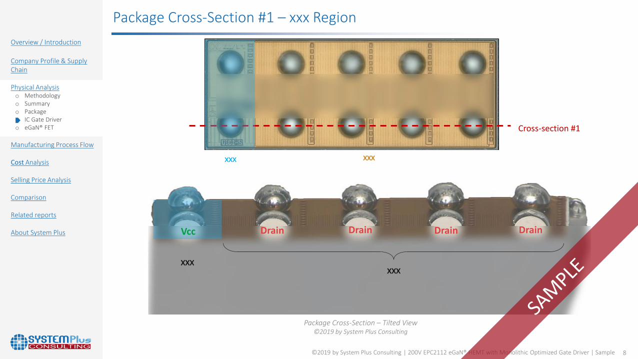
Package Cross-Section #1 – xxx Region
Cross-section #1
Package Cross-Section – Tilted View©2019 by System Plus Consulting
xxx
xxxxxx
xxx
Drain Drain DrainDrainVcc

9©2019 by System Plus Consulting | 200V EPC2112 eGaN® HEMT with Monolithic Optimized Gate Driver | Sample
Overview / Introduction
Company Profile & SupplyChain
Physical Analysis o Methodologyo Summaryo Packageo IC Gate Drivero eGaN® FET
Manufacturing Process Flow
Cost Analysis
Selling Price Analysis
Comparison
Related reports
About System Plus
Package Cross-Section #1
Cross-section #1
Package Cross-Section – Optical View©2019 by System Plus Consulting
xx xx
xx xx
xx µm
o Substrate thickness: xx µm
xx µm

10©2019 by System Plus Consulting | 200V EPC2112 eGaN® HEMT with Monolithic Optimized Gate Driver | Sample
Overview / Introduction
Company Profile & SupplyChain
Physical Analysis o Methodologyo Summaryo Packageo IC Gate Drivero eGaN® FET
Manufacturing Process Flow
Cost Analysis
Selling Price Analysis
Comparison
Related reports
About System Plus
Package Cross-Section #1 – xx
Die Cross-Section – SEM View©2019 by System Plus Consulting
Solder ball in xx
xx layer xx
xx layer xx
xx substrate
xx: xx µmxx layerXx layer
xx
xx layer xx µm
xx layer xx µm
xx layer xx µm
xx layer xx
xx layer xx
xx layers xx µm + xx µm
xx layer xx µm
xx/xx layer xx µm
Die Cross-Section – SEM View©2019 by System Plus Consulting
xx: xx µm
o xx: xx µm
o xx: xx µm
o Xx: xx µm
xx
xx
M1

11©2019 by System Plus Consulting | 200V EPC2112 eGaN® HEMT with Monolithic Optimized Gate Driver | Sample
Overview / Introduction
Company Profile & SupplyChain
Physical Analysis o Methodologyo Summaryo Packageo IC Gate Drivero eGaN® FET
Manufacturing Process Flow
Cost Analysis
Selling Price Analysis
Comparison
Related reports
About System Plus
Package Cross-Section #2 – xx
xxSolder ball xx µm
xx substrate
Die Cross-Section – SEM View©2019 by System Plus Consulting
xx: xx
xx substrate
Die Cross-Section – SEM View©2019 by System Plus Consulting
xx layer
Solder ball in xx
xx layer
xx layer
xx layerxx µm
xx µm
Die Cross-Section – SEM View©2019 by System Plus Consulting
Via xx-xx

12©2019 by System Plus Consulting | 200V EPC2112 eGaN® HEMT with Monolithic Optimized Gate Driver | Sample
Overview / Introduction
Company Profile & SupplyChain
Physical Analysis o Methodologyo Summaryo Packageo IC Gate Drivero eGaN® FET
Manufacturing Process Flow
Cost Analysis
Selling Price Analysis
Comparison
Related reports
About System Plus
Die Process – xx Delayering
Die after Delayering – Optical View©2019 by System Plus Consulting
13©2019 by System Plus Consulting | 200V EPC2112 eGaN® HEMT with Monolithic Optimized Gate Driver | Sample
Overview / Introduction
Company Profile & SupplyChain
Physical Analysis o Methodologyo Summaryo Packageo IC Gate Drivero eGaN® FET
Manufacturing Process Flow
Cost Analysis
Selling Price Analysis
Comparison
Related reports
About System Plus
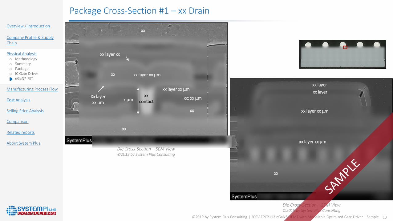
Package Cross-Section #1 – xx Drain
Die Cross-Section – SEM View©2019 by System Plus Consulting
Die Cross-Section – SEM View©2019 by System Plus Consulting
xx layer xx µm
xx
xx
xx layer xx µm
xx layer
xx layerxx layer xx µm
xx: xx µmxx
contactx µmXx layer xx µm
xx layer xx
xx layer xx µmxx
xx
xx
14©2019 by System Plus Consulting | 200V EPC2112 eGaN® HEMT with Monolithic Optimized Gate Driver | Sample
Overview / Introduction
Company Profile & SupplyChain
Physical Analysis o Methodologyo Summaryo Packageo IC Gate Drivero eGaN® FET
Manufacturing Process Flow
Cost Analysis
Selling Price Analysis
Comparison
Related reports
About System Plus
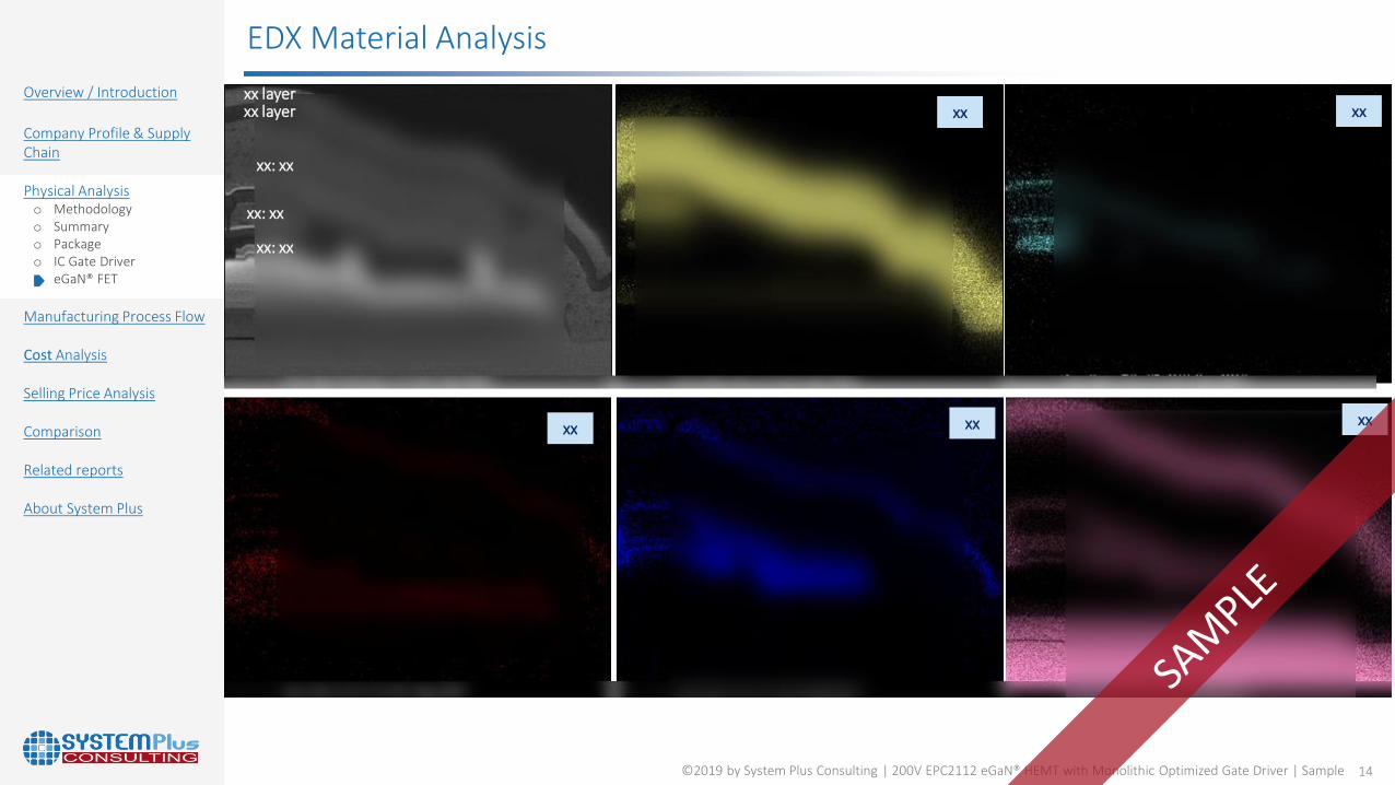
xx xx
xx xx xx
EDX Material Analysis
xx: xx
xx layerxx layer
xx: xx
xx: xx

15©2019 by System Plus Consulting | 200V EPC2112 eGaN® HEMT with Monolithic Optimized Gate Driver | Sample
Overview / Introduction
Company Profile & SupplyChain
Physical Analysis o Methodologyo Summaryo Packageo IC Gate Drivero eGaN® FET
Manufacturing Process Flow
Cost Analysis
Selling Price Analysis
Comparison
Related reports
About System Plus
Package Cross-Section #3 – Contacts
Die Cross-Section – SEM View©2019 by System Plus Consulting
xx
xx µm
Gate contact Drain contactSource contact
xx µm
xx µm
xx µm
xx µm
xx µm
16©2019 by System Plus Consulting | 200V EPC2112 eGaN® HEMT with Monolithic Optimized Gate Driver | Sample
Overview / Introduction
Company Profile & SupplyChain
Physical Analysis o Methodologyo Summaryo Packageo IC Gate Drivero eGaN® FET
Manufacturing Process Flow
Cost Analysis
Selling Price Analysis
Comparison
Related reports
About System Plus
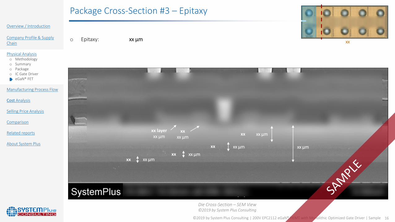
Package Cross-Section #3 – Epitaxy
Die Cross-Section – SEM View©2019 by System Plus Consulting
xx
xx
xx
xx µm
xx µmxx xx µm
xx µm xx µm
o Epitaxy: xx µm xx
xx xx µm
xx layer xx µm
17©2019 by System Plus Consulting | 200V EPC2112 eGaN® HEMT with Monolithic Optimized Gate Driver | Sample
Overview / Introduction
Company Profile & SupplyChain
Physical Analysis o Methodologyo Summaryo Packageo IC Gate Drivero eGaN® FET
Manufacturing Process Flow
Cost Analysis
Selling Price Analysis
Comparison
Related reports
About System Plus
Die Cross-Sections – SEM View©2019 by System Plus Consulting
Mesa: Silicon etch
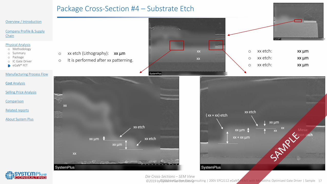
Package Cross-Section #4 – Substrate Etch
xx etch
xx µm
xx µm
xx + xx µm
xx µm
xx µm xx
xx
xx
xxxx
o xx etch (Lithography): xx µm
o It is performed after xx patterning.
o xx etch: xx µm
o xx etch: xx µm
o xx etch: xx µm
xx
xx
xx etch
{ xx + xx} etchxx etch
18©2019 by System Plus Consulting | 200V EPC2112 eGaN® HEMT with Monolithic Optimized Gate Driver | Sample
Overview / Introduction
Company Profile & SupplyChain
Physical Analysis o Methodologyo Summaryo Packageo IC Gate Drivero eGaN® FET
Manufacturing Process Flow
Cost Analysis
Selling Price Analysis
Comparison
Related reports
About System Plus
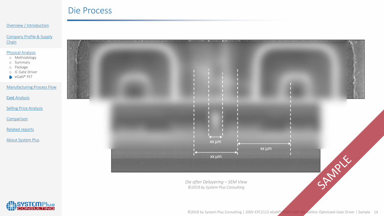
Die Process
89.6 µm
1 µm
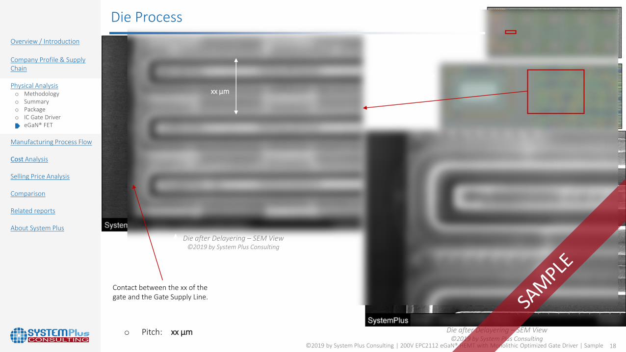
Contact between the xx of the gate and the Gate Supply Line.
Die after Delayering – SEM View©2019 by System Plus Consulting
Die after Delayering – SEM View©2019 by System Plus Consulting
xx µm
o Pitch: xx µm
19©2019 by System Plus Consulting | 200V EPC2112 eGaN® HEMT with Monolithic Optimized Gate Driver | Sample
Overview / Introduction
Company Profile & SupplyChain
Physical Analysis o Methodologyo Summaryo Packageo IC Gate Drivero eGaN® FET
Manufacturing Process Flow
Cost Analysis
Selling Price Analysis
Comparison
Related reports
About System Plus xx µm
Die Process
xx µm
xx µm
Die after Delayering – SEM View©2019 by System Plus Consulting

20©2019 by System Plus Consulting | 200V EPC2112 eGaN® HEMT with Monolithic Optimized Gate Driver | Sample
Overview / Introduction
Company Profile & SupplyChain
Physical Analysis
Manufacturing Process Flowo Wafer Front-End Fab Unito Front-End Process Flowo Packaging Fab Unito Back-End Process Flow
Cost Analysis
Selling Price Analysis
Comparison
Related reports
About System Plus
GaN Transistor - Process Flow (3/4)
Isolation
• xx & xx deposition and pattern
Metal 1
• xx deposition and pattern
Metal 1 and
IMD1
• xx/xx deposition and pattern
• Isolation depositions
xx
xx
xx/xxxx/xx/xx/xx
Drawing not to Scale
21©2019 by System Plus Consulting | 200V EPC2112 eGaN® HEMT with Monolithic Optimized Gate Driver | Sample
Overview / Introduction
Company Profile & SupplyChain
Physical Analysis
Manufacturing Process Flowo Wafer Front-End Fab Unito Front-End Process Flowo Packaging Fab Unito Back-End Process Flow
Cost Analysis
Selling Price Analysis
Comparison
Related reports
About System Plus
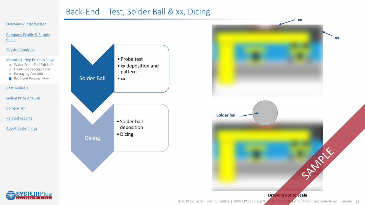
Back-End – Test, Solder Ball & xx, Dicing
Solder Ball
•Probe test
• xx deposition and pattern
• xx
Dicing
• Solder ball deposition
•Dicing
Drawing not to Scale
Solder ball
xx
xx

22©2019 by System Plus Consulting | 200V EPC2112 eGaN® HEMT with Monolithic Optimized Gate Driver | Sample
Overview / Introduction
Company Profile & SupplyChain
Physical Analysis
Manufacturing Process Flow
Cost Analysiso Summaryo Wafer Costo Packaging Costo Die Costo Component Cost
Selling Price Analysis
Comparison
Related reports
About System Plus
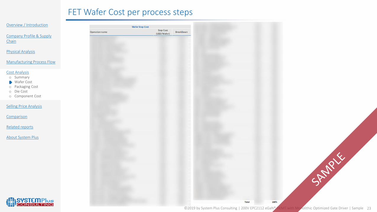
Wafer Front-End Cost
The front-end cost ranges from $xx to $xx according toyield variations.
The main part of the wafer cost is due to the xx with xx%.
23©2019 by System Plus Consulting | 200V EPC2112 eGaN® HEMT with Monolithic Optimized Gate Driver | Sample
Overview / Introduction
Company Profile & SupplyChain
Physical Analysis
Manufacturing Process Flow
Cost Analysiso Summaryo Wafer Costo Packaging Costo Die Costo Component Cost
Selling Price Analysis
Comparison
Related reports
About System Plus
FET Wafer Cost per process steps

24©2019 by System Plus Consulting | 200V EPC2112 eGaN® HEMT with Monolithic Optimized Gate Driver | Sample
Overview / Introduction
Company Profile & SupplyChain
Physical Analysis
Manufacturing Process Flow
Cost Analysiso Summaryo Wafer Costo Packaging Costo Die Costo Component Cost
Selling Price Analysis
Comparison
Related reports
About System Plus
Packaging Cost
Packaging
The component has not packaging, but connection with solder balls. These connections are assumed to bemanufactured by an OSAT.
The cost is estimated between $xx and $xx per wafer.
25©2019 by System Plus Consulting | 200V EPC2112 eGaN® HEMT with Monolithic Optimized Gate Driver | Sample
Overview / Introduction
Company Profile & SupplyChain
Physical Analysis
Manufacturing Process Flow
Cost Analysiso Summaryo Wafer Costo Packaging Costo Die Costo Component Cost
Selling Price Analysis
Comparison
Related reports
About System Plus
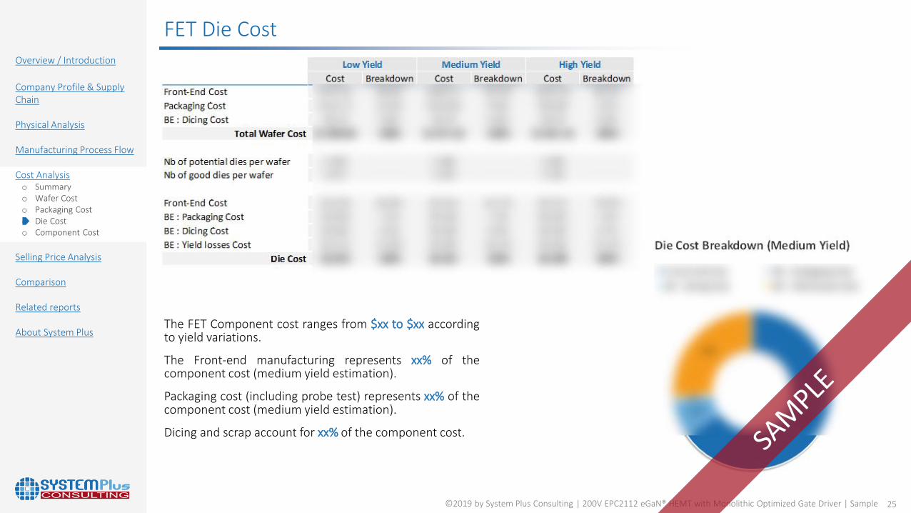
FET Die Cost
The FET Component cost ranges from $xx to $xx accordingto yield variations.
The Front-end manufacturing represents xx% of thecomponent cost (medium yield estimation).
Packaging cost (including probe test) represents xx% of thecomponent cost (medium yield estimation).
Dicing and scrap account for xx% of the component cost.
26©2019 by System Plus Consulting | 200V EPC2112 eGaN® HEMT with Monolithic Optimized Gate Driver | Sample
Overview / Introduction
Company Profile & SupplyChain
Physical Analysis
Manufacturing Process Flow
Cost Analysiso Summaryo Wafer Costo Packaging Costo Die Costo Component Cost
Selling Price Analysis
Comparison
Related reports
About System Plus
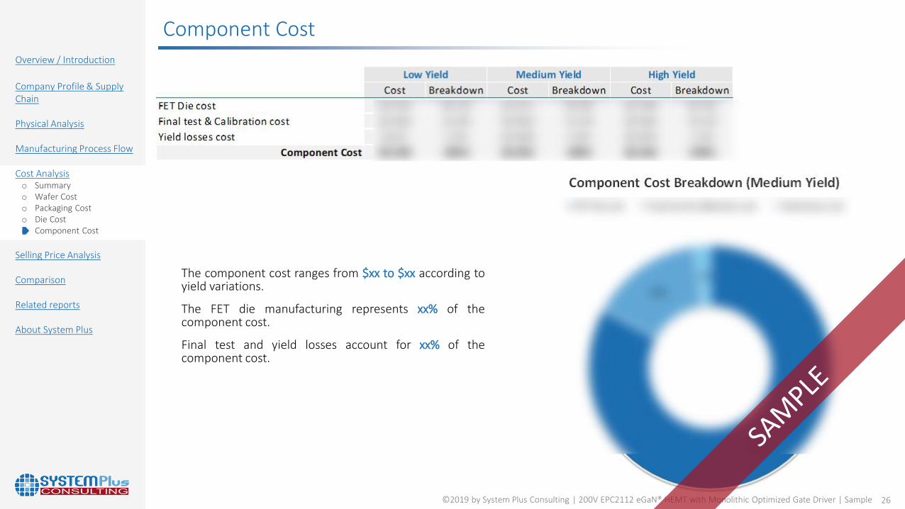
Component Cost
The component cost ranges from $xx to $xx according toyield variations.
The FET die manufacturing represents xx% of thecomponent cost.
Final test and yield losses account for xx% of thecomponent cost.
27©2019 by System Plus Consulting | 200V EPC2112 eGaN® HEMT with Monolithic Optimized Gate Driver | Sample
Overview / Introduction
Company Profile & Supply Chain
Physical Analysis
Manufacturing Process Flow
Cost Analysis
Selling Price Analysis
Comparison
Related reports
About System Plus
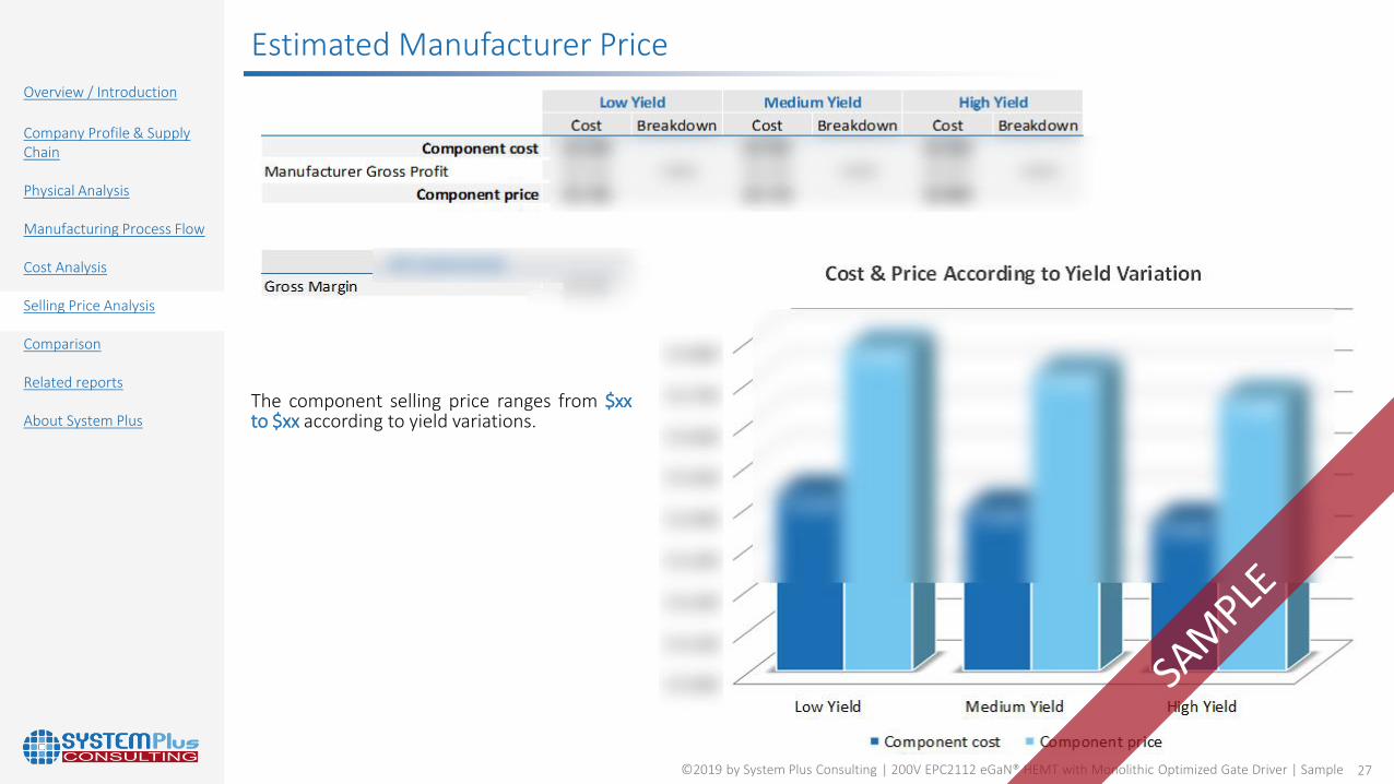
Estimated Manufacturer Price
The component selling price ranges from $xxto $xx according to yield variations.
28©2019 by System Plus Consulting | 200V EPC2112 eGaN® HEMT with Monolithic Optimized Gate Driver | Sample
Overview / Introduction
Company Profile & Supply Chain
Physical Analysis
Manufacturing Process Flow
Cost Analysis
Selling Price Analysis
Comparisono EPC vs Navitas GaN FETo 200V EPC eGaN® FETs
Related reports
About System Plus
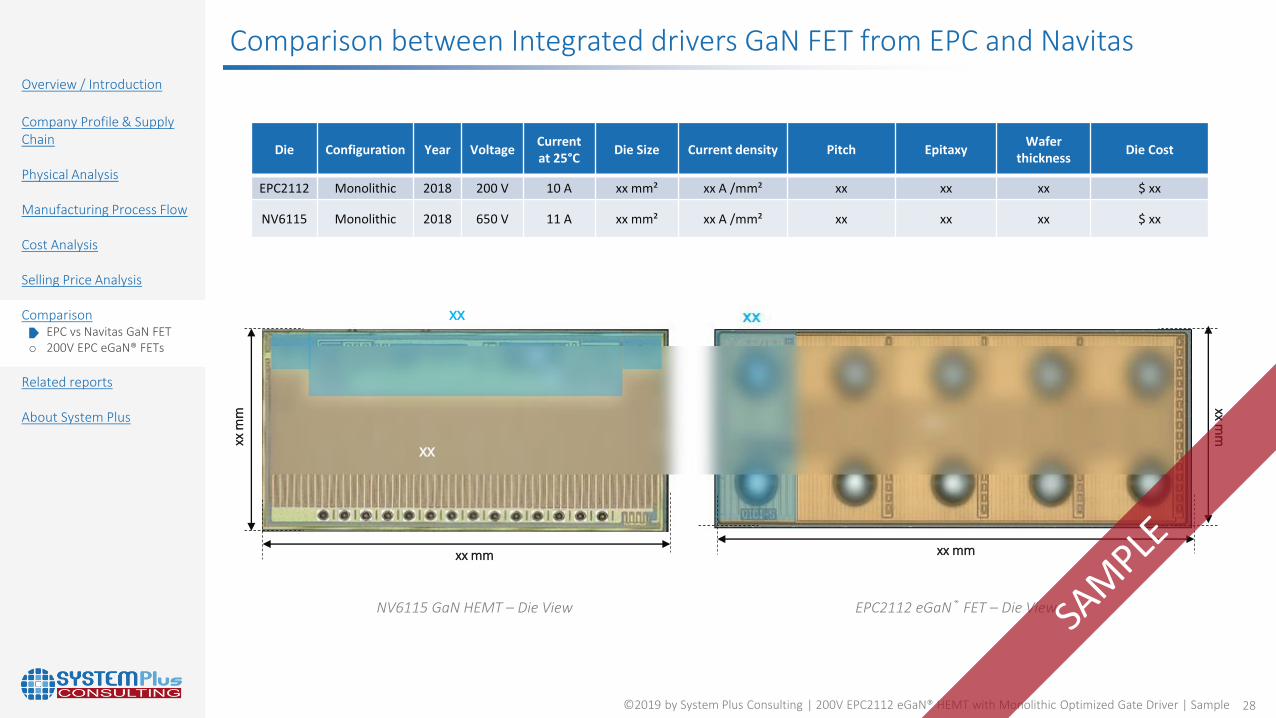
Die Configuration Year VoltageCurrent at 25°C
Die Size Current density Pitch EpitaxyWafer
thicknessDie Cost
EPC2112 Monolithic 2018 200 V 10 A xx mm² xx A /mm² xx xx xx $ xx
NV6115 Monolithic 2018 650 V 11 A xx mm² xx A /mm² xx xx xx $ xx
Comparison between Integrated drivers GaN FET from EPC and Navitas
NV6115 GaN HEMT – Die View EPC2112 eGaN® FET – Die View
xx
xx
xx m
m
xx mm xx mm
xx mm
29©2019 by System Plus Consulting | 200V EPC2112 eGaN® HEMT with Monolithic Optimized Gate Driver | Sample
Overview / Introduction
Company Profile & Supply Chain
Physical Analysis
Manufacturing Process Flow
Cost Analysis
Selling Price Analysis
Comparisono EPC vs Navitas GaN FETo 200V EPC eGaN® FETs
Related reports
About System Plus
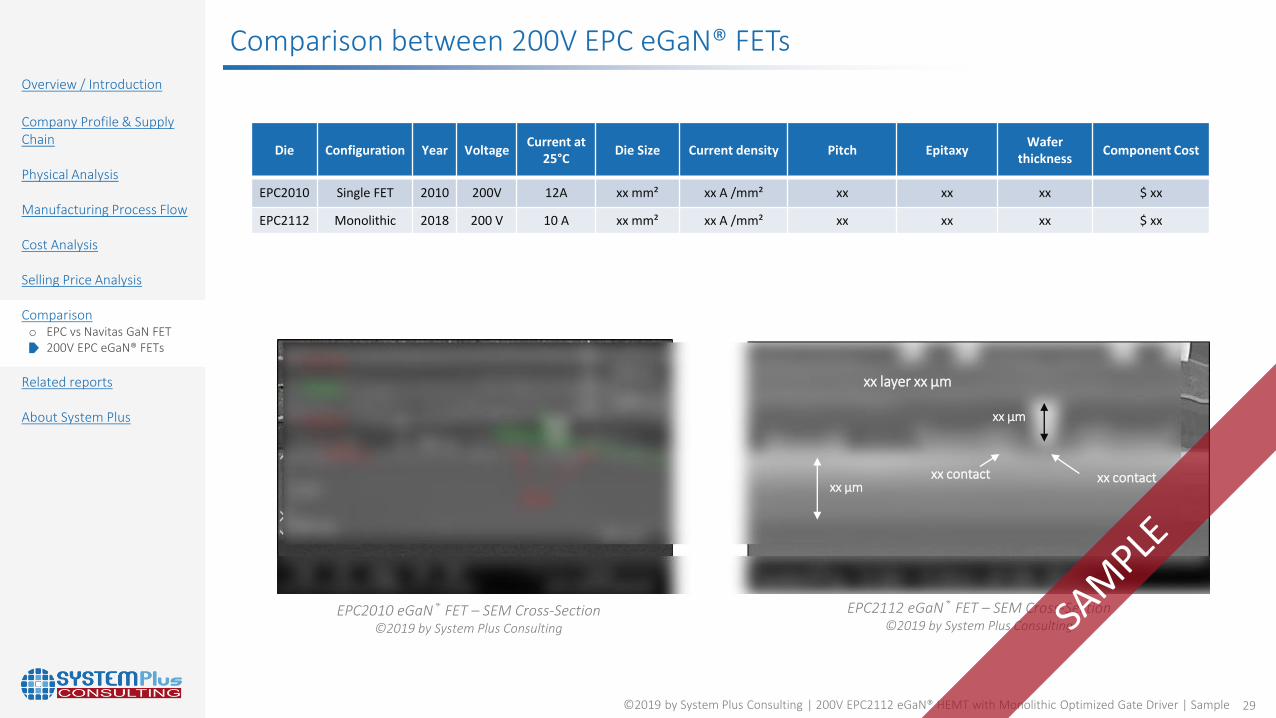
Die Configuration Year VoltageCurrent at
25°CDie Size Current density Pitch Epitaxy
Wafer thickness
Component Cost
EPC2010 Single FET 2010 200V 12A xx mm² xx A /mm² xx xx xx $ xx
EPC2112 Monolithic 2018 200 V 10 A xx mm² xx A /mm² xx xx xx $ xx
Comparison between 200V EPC eGaN® FETs
xx contact xx contactxx µm
EPC2112 eGaN® FET – SEM Cross-Section©2019 by System Plus Consulting
EPC2010 eGaN® FET – SEM Cross-Section©2019 by System Plus Consulting
xx µm
xx layer xx µm

30©2019 by System Plus Consulting | 200V EPC2112 eGaN® HEMT with Monolithic Optimized Gate Driver | Sample
Overview / Introduction
Company Profile & Supply Chain
Physical Analysis
Manufacturing Process Flow
Cost Analysis
Selling Price Analysis
Comparison
Related reports
About System Plus
REVERSE COSTING ANALYSES - SYSTEM PLUS CONSULTING
Power Semiconductors & Compound• GaN-on-Sapphire HEMT Power IC by Power Integrations• Navitas 650V GaNFast Power IC Family• Transphorm GaN-on-Silicon HEMT TPH3• GaN-on-Silicon Transistor Comparison 2018
Related Reports
MARKET AND TECHNOLOGY REPORTS - YOLE DÉVELOPPEMENT
POWER ELECTRONICS & COMPOUND SEMI• Power GaN 2018: Epitaxy, Devices, Applications and Technology
Trends• Status of the Power Electronics Industry 2019• Wireless Charging Technologies and Markets 2018

31©2019 by System Plus Consulting | 200V EPC2112 eGaN® HEMT with Monolithic Optimized Gate Driver | Sample
COMPANYSERVICES
32©2019 by System Plus Consulting | 200V EPC2112 eGaN® HEMT with Monolithic Optimized Gate Driver | Sample
Overview / Introduction
Company Profile & Supply Chain
Physical Analysis
Manufacturing Process Flow
Cost Analysis
Selling Price Analysis
Comparison
Related reports
About System Pluso Company serviceso Contact
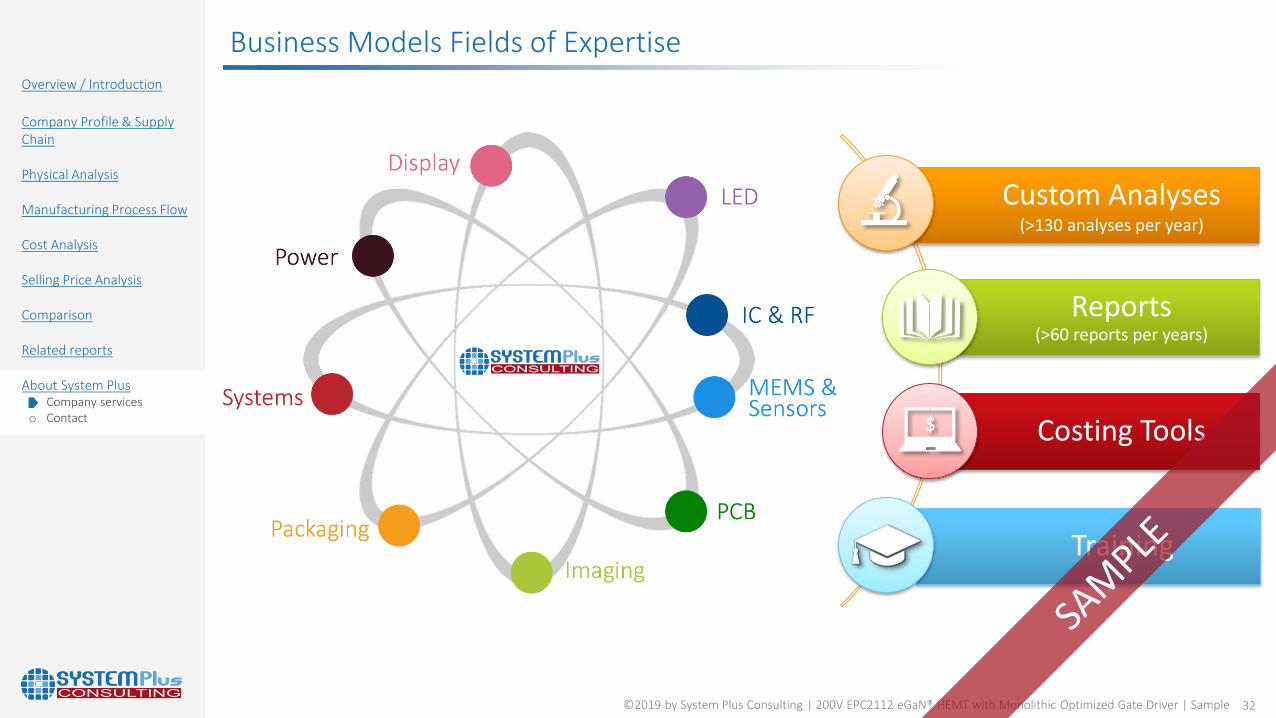
Business Models Fields of Expertise
Custom Analyses(>130 analyses per year)
Reports(>60 reports per years)
Costing Tools
Training
33©2019 by System Plus Consulting | 200V EPC2112 eGaN® HEMT with Monolithic Optimized Gate Driver | Sample
Overview / Introduction
Company Profile & Supply Chain
Physical Analysis
Manufacturing Process Flow
Cost Analysis
Selling Price Analysis
Comparison
Related reports
About System Pluso Company serviceso Contact
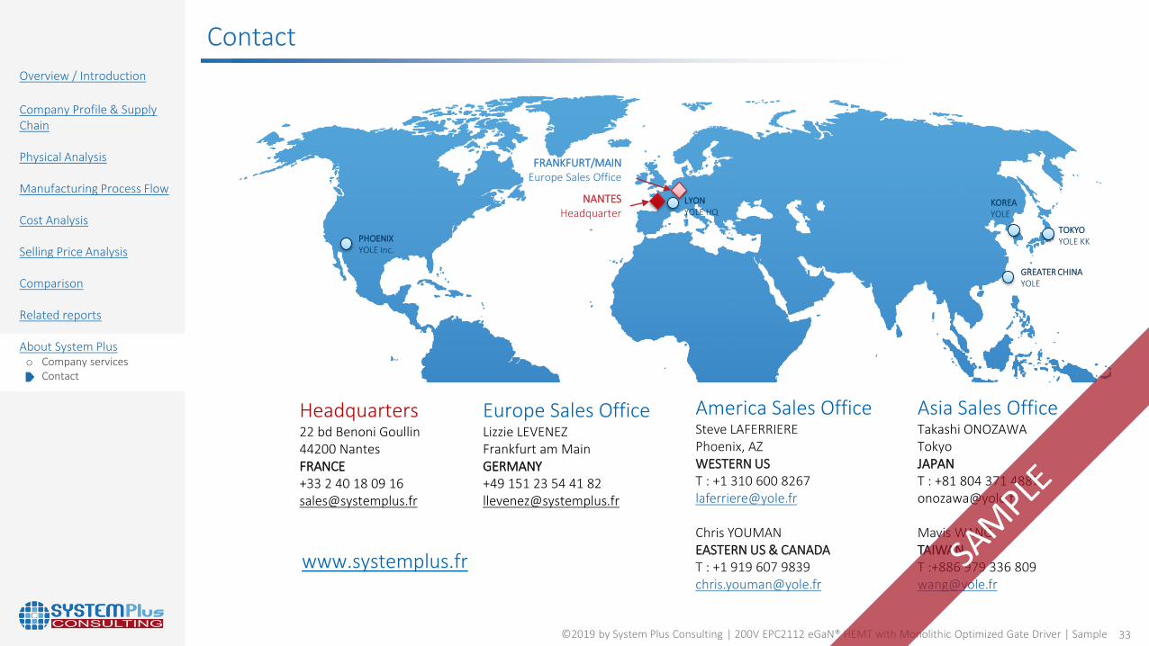
Contact
Headquarters22 bd Benoni Goullin44200 NantesFRANCE+33 2 40 18 09 [email protected]
Europe Sales OfficeLizzie LEVENEZFrankfurt am MainGERMANY+49 151 23 54 41 [email protected]
www.systemplus.fr
Asia Sales OfficeTakashi ONOZAWATokyoJAPANT : +81 804 371 [email protected]
Mavis WANGTAIWANT :+886 979 336 [email protected]
NANTESHeadquarter
FRANKFURT/MAINEurope Sales Office
LYONYOLE HQ
TOKYOYOLE KK
GREATER CHINAYOLE
PHOENIXYOLE Inc.
KOREAYOLE
America Sales OfficeSteve LAFERRIEREPhoenix, AZWESTERN UST : +1 310 600 [email protected]
Chris YOUMANEASTERN US & CANADAT : +1 919 607 9839 [email protected]

ORDER FORMPlease process my order for “200V EPC2112 eGaN® HEMT with Monolithic Optimized Gate Driver” Reverse Costing® – Structure, Process & Cost Report Ref: SP19415
Full Structure, Process & Cost Report : EUR 3,990* Annual Subscription offers possible from 3 reports, including this
report as the first of the year. Contact us for more information.
SHIP TO
Name (Mr/Ms/Dr/Pr): .............................................................
Job Title: …….............................................................................
Company: ….............................................................................
Address: …….............................................................................
City: ………………………………… State: ..........................................
Postcode/Zip: ..........................................................................
Country: ……............................................................................
VAT ID Number for EU members: ..........................................
Tel: ……………….........................................................................
Email: .....................................................................................
Date: ......................................................................................
Signature: ..............................................................................
BILLING CONTACT
First Name : ............................................................................
Last Name: …….......................................................................
Email: …..................................................................................
Phone: ……..............................................................................
PAYMENT
By credit card:
Number: |__|__|__|__| |__|__|__|__| |__|__|__|__|
|__|__|__|__|
Expiration date: |__|__|/|__|__|
Card Verification Value: |__|__|__|
By bank transfer:HSBC - CAE- Le Terminal -2 rue du Charron - 44800 St Herblain FranceBIC code: CCFRFRPP• In EUR
Bank code : 30056 - Branch code : 00955 - Account : 09550003234 IBAN: FR76 3005 6009 5509 5500 0323 439
• In USDBank code : 30056 - Branch code : 00955 - Account : 09550003247 IBAN: FR76 3005 6009 5509 5500 0324 797
REVERSE COSTING® – STRUCTURE, PROCESS & COST REPORT200V EPC2112 EGAN® HEMT
Each year System Plus Consultingreleases a comprehensive collectionof new reverse engineering andcosting analyses in various domains.You can choose to buy over 12months a set of 3, 4, 5, 7, 10 or 15Reverse Costing® reports.
Up to 47% discount!
More than 60 reports released eachyear on the following topics(considered for 2018):• MEMS & Sensors: Accelerometer
– Environment - Fingerprint - Gas - Gyroscope - IMU/Combo -Microphone - Optics - Oscillator -Pressure
• Power: GaN - IGBT - MOSFET - Si Diode - SiC
• Imaging: Camera - Spectrometer• LED and Laser: UV LED – VCSEL -
White/blue LED• Packaging: 3D Packaging -
Embedded - SIP - WLP• Integrated Circuits: IPD –
Memories – PMIC - SoC• RF: FEM - Duplexer• Systems: Automotive - Consumer
- Energy - Telecom
ANNUAL SUBSCRIPTIONS
Return order by: FAX: +33 2 53 55 10 59MAIL: SYSTEM PLUS CONSULTING
22, bd Benoni GoullinNantes Biotech44200 Nantes – France
EMAIL: [email protected]
*For price in dollars please use the day’s exchange rate *All reports are delivered electronically in pdf format*For French customer, add 20 % for VAT*Our prices are subject to change. Please check our new releases and price changes on www.systemplus.fr. The present document is valid 6 months after its publishing date: September 2019

1.INTRODUCTIONThe present terms and conditions apply to the offers, sales and deliveries of services managed by System PlusConsulting except in the case of a particular written agreement.Buyer must note that placing an order means an agreement without any restriction with these terms and conditions.
2.PRICESPrices of the purchased services are those which are in force on the date the order is placed. Prices are in Euros andworked out without taxes. Consequently, the taxes and possible added costs agreed when the order is placed will becharged on these initial prices.System Plus Consulting may change its prices whenever the company thinks it necessary. However, the companycommits itself in invoicing at the prices in force on the date the order is placed.
3.REBATES and DISCOUNTSThe quoted prices already include the rebates and discounts that System Plus Consulting could have granted accordingto the number of orders placed by the Buyer, or other specific conditions. No discount is granted in case of earlypayment.
4.TERMS OF PAYMENTSystem Plus Consulting delivered services are to be paid within 30 days end of month by bank transfer except in thecase of a particular written agreement.If the payment does not reach System Plus Consulting on the deadline, the Buyer has to pay System Plus Consulting apenalty for late payment the amount of which is three times the legal interest rate. The legal interest rate is thecurrent one on the delivery date. This penalty is worked out on the unpaid invoice amount, starting from the invoicedeadline. This penalty is sent without previous notice.When payment terms are over 30 days end of month, the Buyer has to pay a deposit which amount is 10% of the
total invoice amount when placing his order.
5. OWNERSHIPSystem Plus Consulting remains sole owner of the delivered services until total payment of the invoice.
6.DELIVERIESThe delivery schedule on the purchase order is given for information only and cannot be strictly guaranteed.Consequently any reasonable delay in the delivery of services will not allow the buyer to claim for damages or tocancel the order.
7.ENTRUSTED GOODS SHIPMENTThe transport costs and risks are fully born by the Buyer. Should the customer wish to ensure the goods against lost ordamage on the base of their real value, he must imperatively point it out to System Plus Consulting when theshipment takes place. Without any specific requirement, insurance terms for the return of goods will be the carriercurrent ones (reimbursement based on good weight instead of the real value).
8.FORCE MAJEURESystem Plus Consulting responsibility will not be involved in non execution or late delivery of one of its dutiesdescribed in the current terms and conditions if these are the result of a force majeure case. Therefore, the forcemajeure includes all external event unpredictable and irresistible as defined by the article 1148 of the French CodeCivil?
9.CONFIDENTIALITYAs a rule, all information handed by customers to system Plus Consulting are considered as strictly confidential.A non-disclosure agreement can be signed on demand.
10.RESPONSABILITY LIMITATIONThe Buyer is responsible for the use and interpretations he makes of the reports delivered by System Plus Consulting.Consequently, System Plus Consulting responsibility can in no case be called into question for any direct or indirectdamage, financial or otherwise, that may result from the use of the results of our analysis or results obtained usingone of our costing tools.
11.APPLICABLE LAWAny dispute that may arise about the interpretation or execution of the current terms and conditions shall be resolvedapplying the French law.It the dispute cannot be settled out-of-court, the competent Court will be the Tribunal de Commerce de Nantes.
TERMS AND CONDITIONS OF SALES