vturesource.weebly.comvturesource.weebly.com/uploads/3/7/4/0/37406139/basic... · 2019-10-09 ·...
TRANSCRIPT


SHREE PILLAPPA COLLEGE OF ENGINEERING, KONDASHETTIHALLI ROAD, BENGALURU-89 Ph no: 9742174174, 9844231315
SHASHIDHAR T M B.E (SJMIT), M.Tech (PESIT), M.Sc( Maths), (Ph.D (RVCE)) , Asst. Professor, ECE Dept.
QUESTION BANK
Sub: Basic Electronics Sub Code: 15ELN15
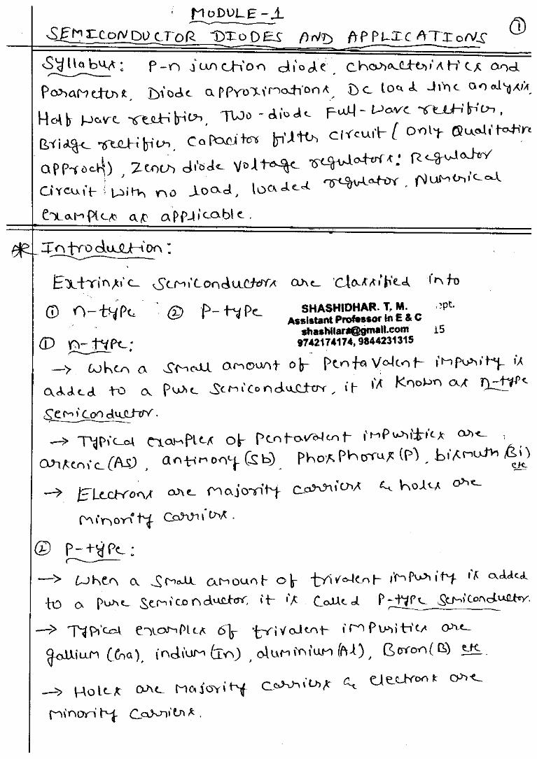
MODULE I: a) Semiconductors diodes and its applications
1. Define the following diode parameters: a) Forward voltage b) Knee voltage
c) Dynamic resistance d) Reverse saturation Current e) PIV
f)Reverse recovery time g)Reverse breakdown voltage h)Forward
recovery time i)reverse recovery time
2. Explain the quantitative theory of unbiased p-n junction.
3. What do you mean by biasing the pn junction? Explain briefly.
4. Explain the V-I characteristics with respect to the Shockley equation.
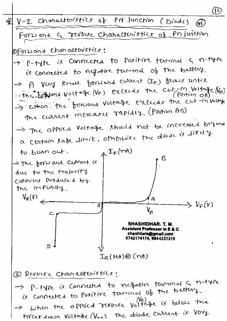
5. Draw and explain V-I characteristics of p-n junction diode.
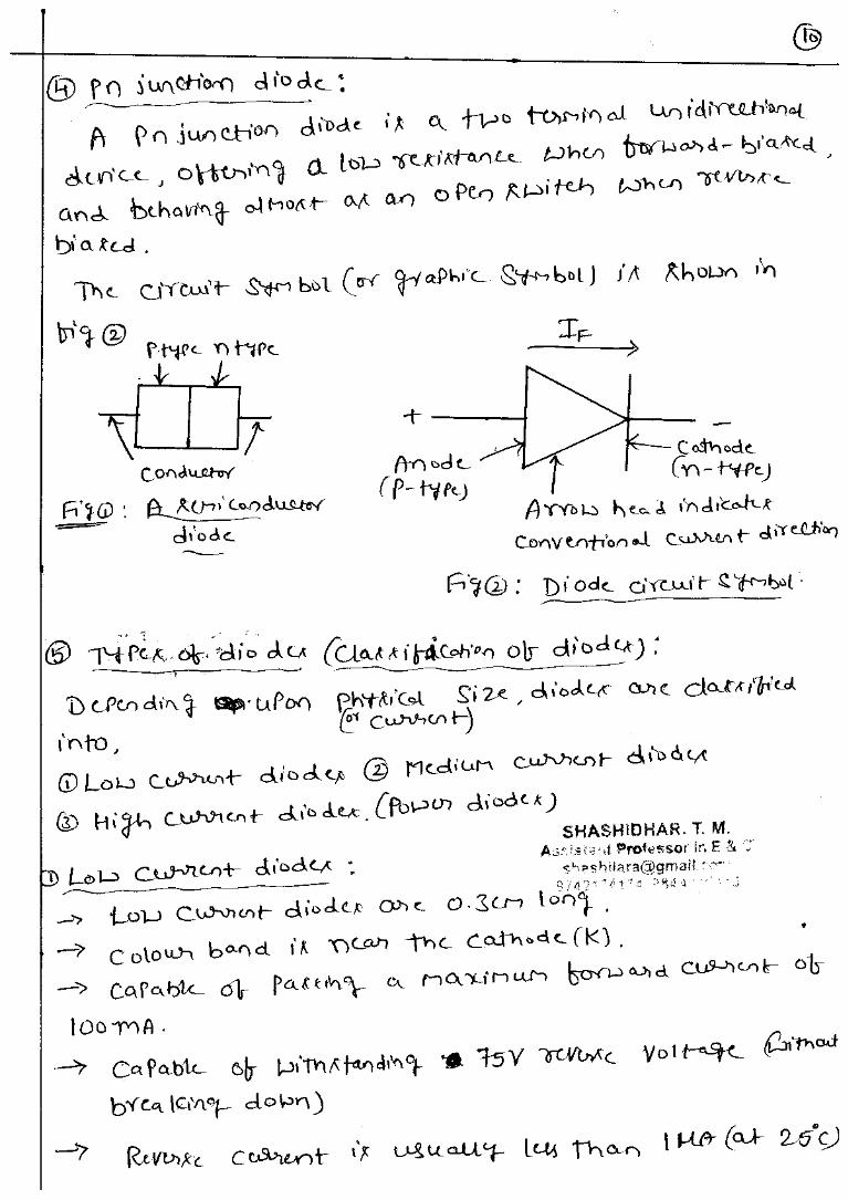
6. Discuss on types of diodes.
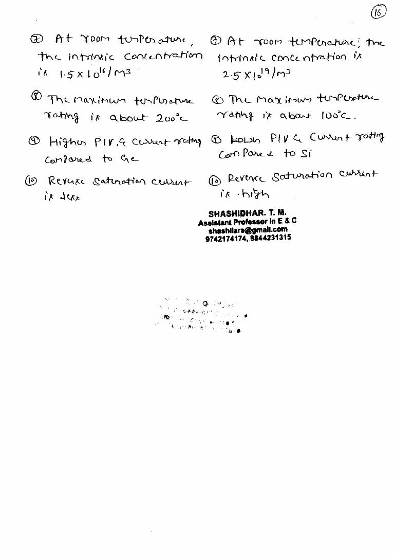
7. What is the effect of temperature on cut-in voltage and reverse saturation
current?
8. Differentiate between diffusion and transition capacitance.
9. Differentiate between Zener breakdown and Avalanche breakdown
10. Draw the volt- ampere characteristics of Si & Ge diode, explain briefly.
11. Explain DC equivalent circuits of pn junction.
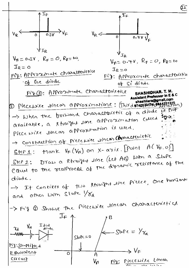
12. Discuss on the diode approximations.
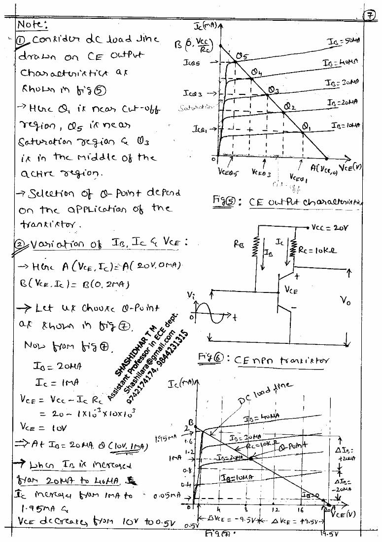
13. What is dc load line? Explain briefly. Give the significance of Q-point.
14. Expalin the following terms w r t pn junction:
a)DC resistance b) AC resistance
15. With a neat circuit diagram and wave forms, explain the operation of Half-
wave rectifier. Also mention its merits and demerits.
16. Explain Zener diode voltage regulator circuit with no load and with load.
17. Explain the working of a full wave bridge rectifier with the help of circuit
diagram and wave forms. Also mention its merits and demerits.
18. With a neat circuit diagram and waveforms, explain the working of FWR.
Also mention its merits and demerits.

SHREE PILLAPPA COLLEGE OF ENGINEERING, KONDASHETTIHALLI ROAD, BENGALURU-89 Ph no: 9742174174, 9844231315
SHASHIDHAR T M B.E (SJMIT), M.Tech (PESIT), M.Sc( Maths), (Ph.D (RVCE)) , Asst. Professor, ECE Dept.
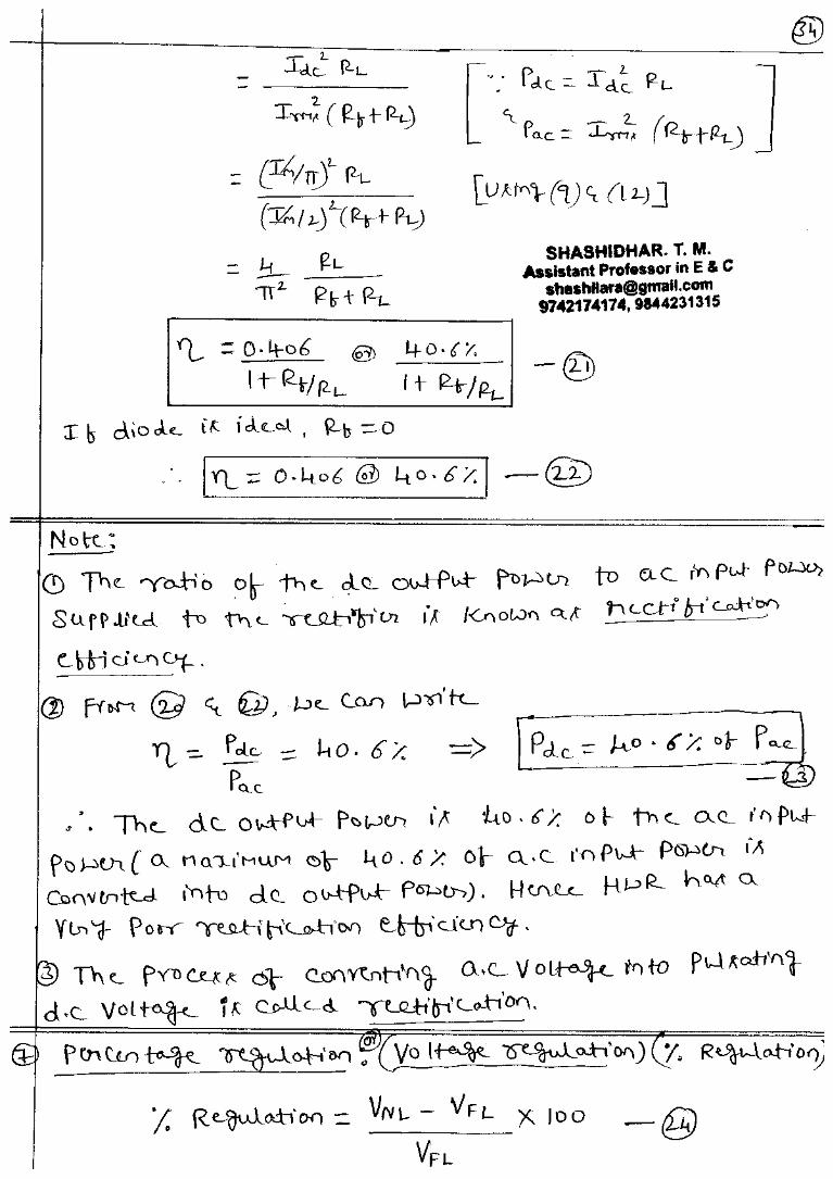
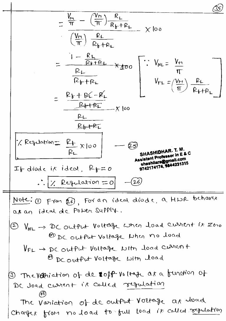
19. For HWR, derive an expression for a)DC load current b) Average load
voltage c) RMS load current d) RMS load voltage e)Ripple factor f) Efficiency
g)Percentage regulation h)PIV
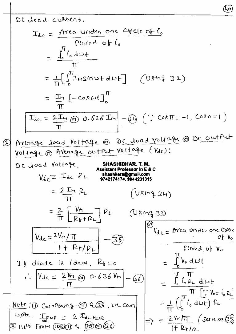
20. For FWR, derive an expression for a)DC load current b) Average load
voltage c) RMS load current d) RMS load voltage e)Ripple factor f) Efficiency
g)Percentage regulation h)PIV
21. For FWBR, derive an expression for a)DC load current b) Average load
voltage c) RMS load current d) RMS load voltage e)Ripple factor f) Efficiency
g)Percentage regulation h)PIV
22. What is filter? List the types of filters.
23. With a neat circuit diagram and waveforms, explain the working of HWR with
‘C’ filter.
24. With a neat circuit diagram and waveforms, explain the working of FWR with
‘C’ filter.
25. With a neat circuit diagram and waveforms, explain the working of FWBR
with ‘C’ filter.
26. State the advantages and disadvantages of capacitor filter.
27. Explain briefly line and load regulation.
MODULE 1: b) Bipolar Junction Transistors
1. Draw an unbiased NPN transistor. Label it and show the depletion regions
and barrier potentials. Explain briefly.
2. With a neat diagram, explain unbiased PNP transistor.
3. Discuss on the operating regions of a transistor.
4. Discuss on the types of BJTs.
5. With a neat diagram, explain biased NPN transistor.
6. With a neat diagram, explain biased PNP transistor.
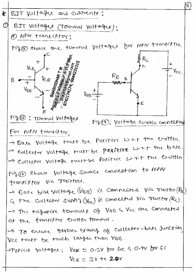
7. Discuss on BJT voltages and currents.
8. Discuss on the different configurations of BJT.
9. Define current gain of CB, CE and CC transistor configurations.
SHREE PILLAPPA COLLEGE OF ENGINEERING, KONDASHETTIHALLI ROAD, BENGALURU-89 Ph no: 9742174174, 9844231315
SHASHIDHAR T M B.E (SJMIT), M.Tech (PESIT), M.Sc( Maths), (Ph.D (RVCE)) , Asst. Professor, ECE Dept.
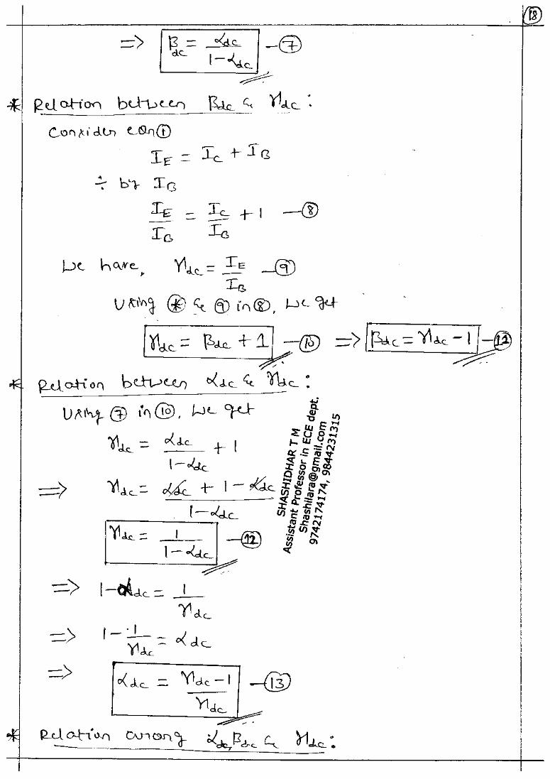
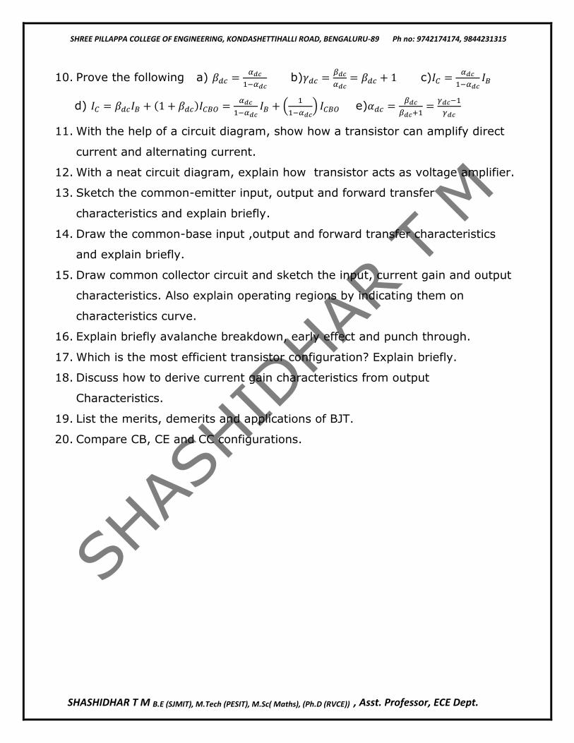
10. Prove the following a) 𝛽𝑑𝑐 =𝛼𝑑𝑐
1−𝛼𝑑𝑐 b)𝛾𝑑𝑐 =
𝛽𝑑𝑐
𝛼𝑑𝑐= 𝛽𝑑𝑐 + 1 c)𝐼𝐶 =
𝛼𝑑𝑐
1−𝛼𝑑𝑐𝐼𝐵
d) 𝐼𝐶 = 𝛽𝑑𝑐𝐼𝐵 + (1 + 𝛽𝑑𝑐)𝐼𝐶𝐵𝑂 =𝛼𝑑𝑐
1−𝛼𝑑𝑐𝐼𝐵 + (
1
1−𝛼𝑑𝑐) 𝐼𝐶𝐵𝑂 e)𝛼𝑑𝑐 =
𝛽𝑑𝑐
𝛽𝑑𝑐+1=
𝛾𝑑𝑐−1
𝛾𝑑𝑐
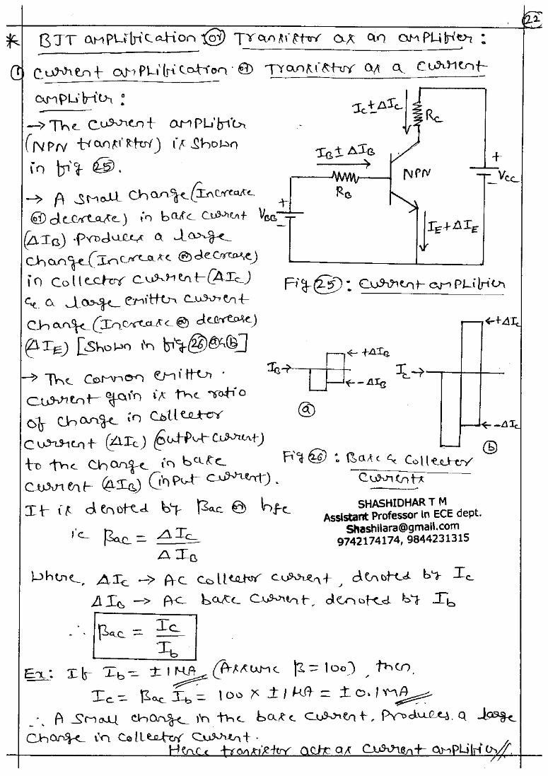
11. With the help of a circuit diagram, show how a transistor can amplify direct
current and alternating current.
12. With a neat circuit diagram, explain how transistor acts as voltage amplifier.
13. Sketch the common-emitter input, output and forward transfer
characteristics and explain briefly.
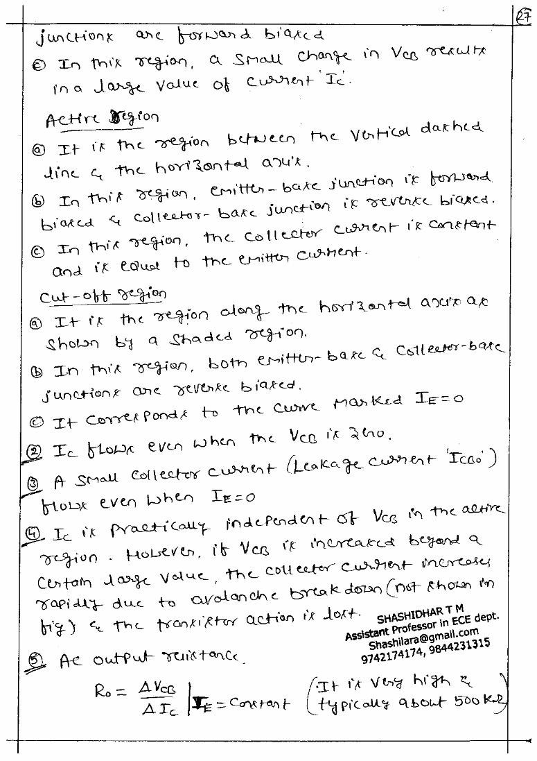
14. Draw the common-base input ,output and forward transfer characteristics
and explain briefly.
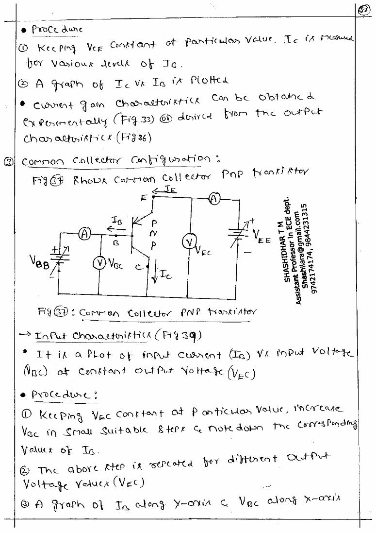
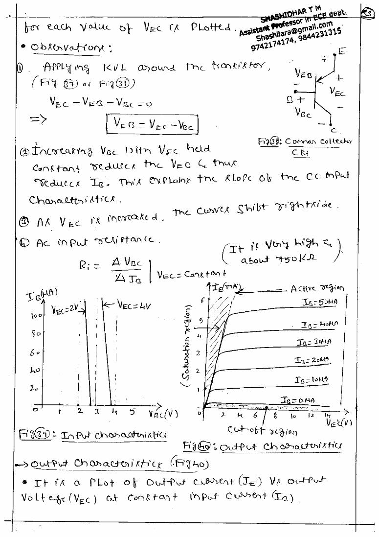
15. Draw common collector circuit and sketch the input, current gain and output
characteristics. Also explain operating regions by indicating them on
characteristics curve.
16. Explain briefly avalanche breakdown, early effect and punch through.
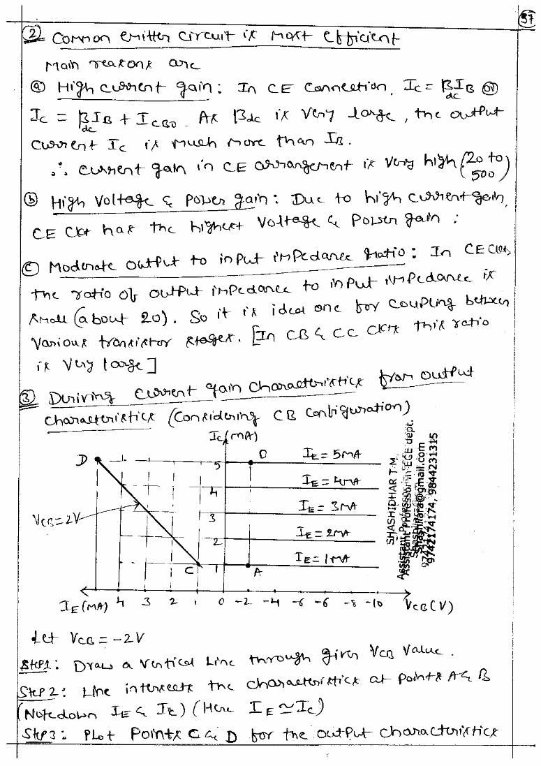
17. Which is the most efficient transistor configuration? Explain briefly.
18. Discuss how to derive current gain characteristics from output
Characteristics.
19. List the merits, demerits and applications of BJT.
20. Compare CB, CE and CC configurations.

SHREE PILLAPPA COLLEGE OF ENGINEERING, KONDASHETTIHALLI ROAD, BENGALURU-89 Ph no: 9742174174, 9844231315
SHASHIDHAR T M B.E (SJMIT), M.Tech (PESIT), M.Sc( Maths), (Ph.D (RVCE)) , Asst. Professor, ECE Dept.
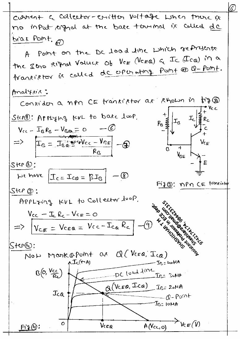
Module 2: a) Transistors Biasing
1. Explain the operation of the base bias circuit using an NPN transistor and
write the expressions for IB,IC and VCE .
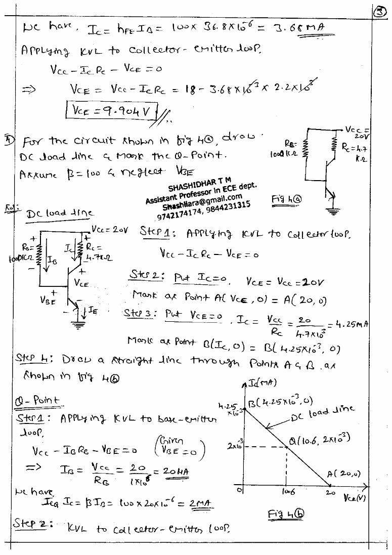
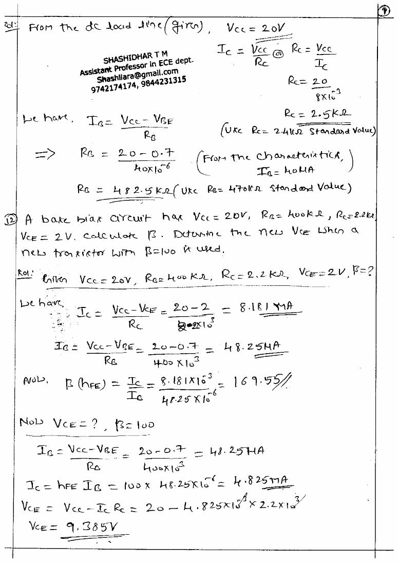
2. What is Dc load line? Explain Base bias method with necessary equations.
3. What do you mean by biasing the transistor?
4. Explain the need for biasing the transistor.
5. What do you mean by silent point? Explain briefly.
6. Show that for a maximum undistorted output, the transistor should be
driven into active region.
7. Discuss on the design of base-bias circuit.
8. Explain the operation of the base bias circuit using an pnp transistor and
write the expressions for IB,IC and VCE .
9. State the merits, demerits and usage of base bias circuit.
10. Discuss on the factors affecting the stability of Q-point.
11. Sketch a universal bias circuit using an pnp transistor.
12. Compare base-bias and self bias circuits.
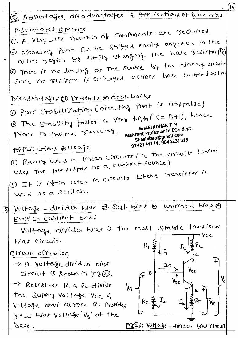
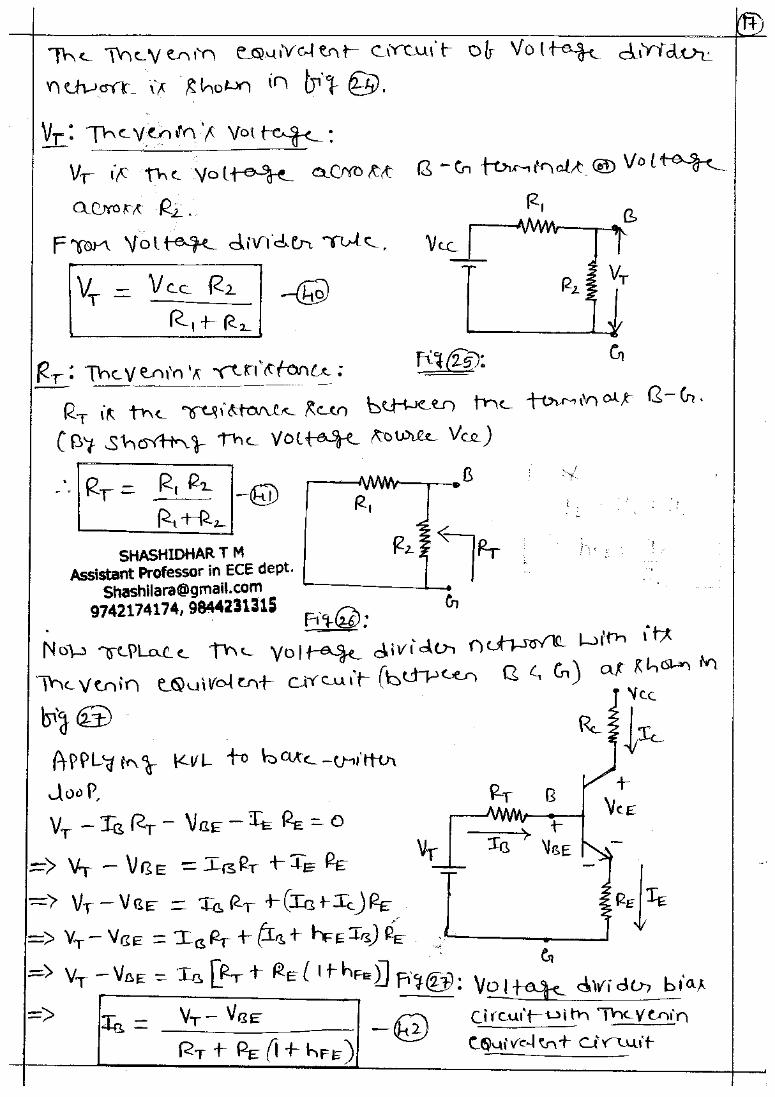
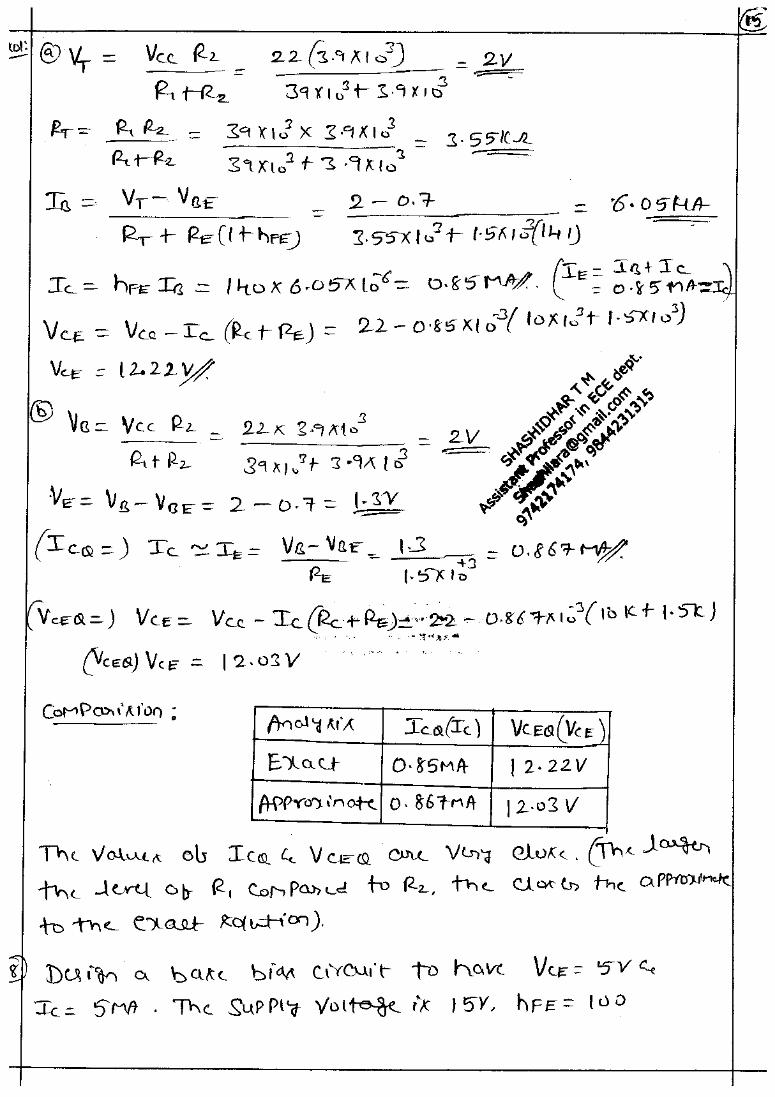
13. Discuss on the design of Voltage divider bias circuit.
14. With a neat circuit diagram, explain the Emitter current bias circuit using
a) Approximate analysis. b) Precise analysis.
15. Define the stability factor of transistor circuit.
16. Draw Dc load line and locate Q-point for a Voltage-divider bias circuit.
17. State the merits, demerits and usage of voltage divider bias circuit.
MODULE 2: b) OP Amp
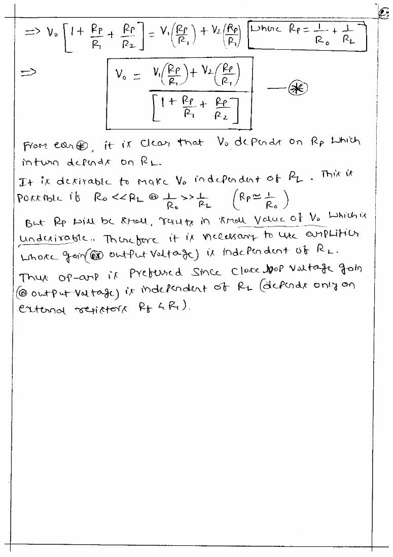
1. What is an Op-Amp? What are the basic properties of an Op-Amp
2. State the applications of Op-Amp.
3. Draw the pin diagram, circuit symbol and Circuit model of Op-Amp.
4. Mention the features of 𝜇𝐴 741.
5. State the advantages of Op-Amp over transistor amplifier.

SHREE PILLAPPA COLLEGE OF ENGINEERING, KONDASHETTIHALLI ROAD, BENGALURU-89 Ph no: 9742174174, 9844231315
SHASHIDHAR T M B.E (SJMIT), M.Tech (PESIT), M.Sc( Maths), (Ph.D (RVCE)) , Asst. Professor, ECE Dept.
6. With a neat block diagram, explain the architecture of Op-Amp.
7. Discuss on saturation property of Op-Amp.
8. Explain the different configurations of an Op-amp.
9. With usual notations, show that the total output of an Op-amp(differential
amplifier) is given by, 𝑉𝑜 = 𝐴𝑑𝑉𝑑(1 +1
𝐶𝑀𝑅𝑅 𝑉𝑐𝑚
𝑉𝑑)
10. Explain the concept of virtual short.
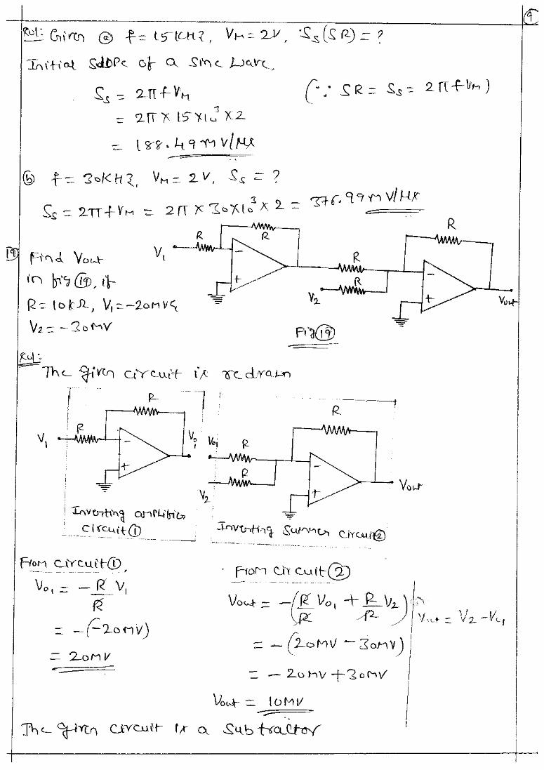
11. Prove that for an undistorted output voltage, the maximum signal frequency
is given by, 𝑓𝑚𝑎𝑥 =𝑆𝑅
2𝜋𝑉𝑚(𝐻𝑧) or 𝜔𝑚𝑎𝑥 =
𝑆𝑅
𝑉𝑚(𝑟𝑎𝑑/𝑠)
12. Define the following Op-amp parameters.
a)Large signal voltage gain b) Common mode gain c) CMRR
d) Input impedance d)Output resistance e)BW
f)Input Offset voltage g)Output Offset voltage h)SR
i) Input Offset current j)Input bias current k)SVRR(PSRR)
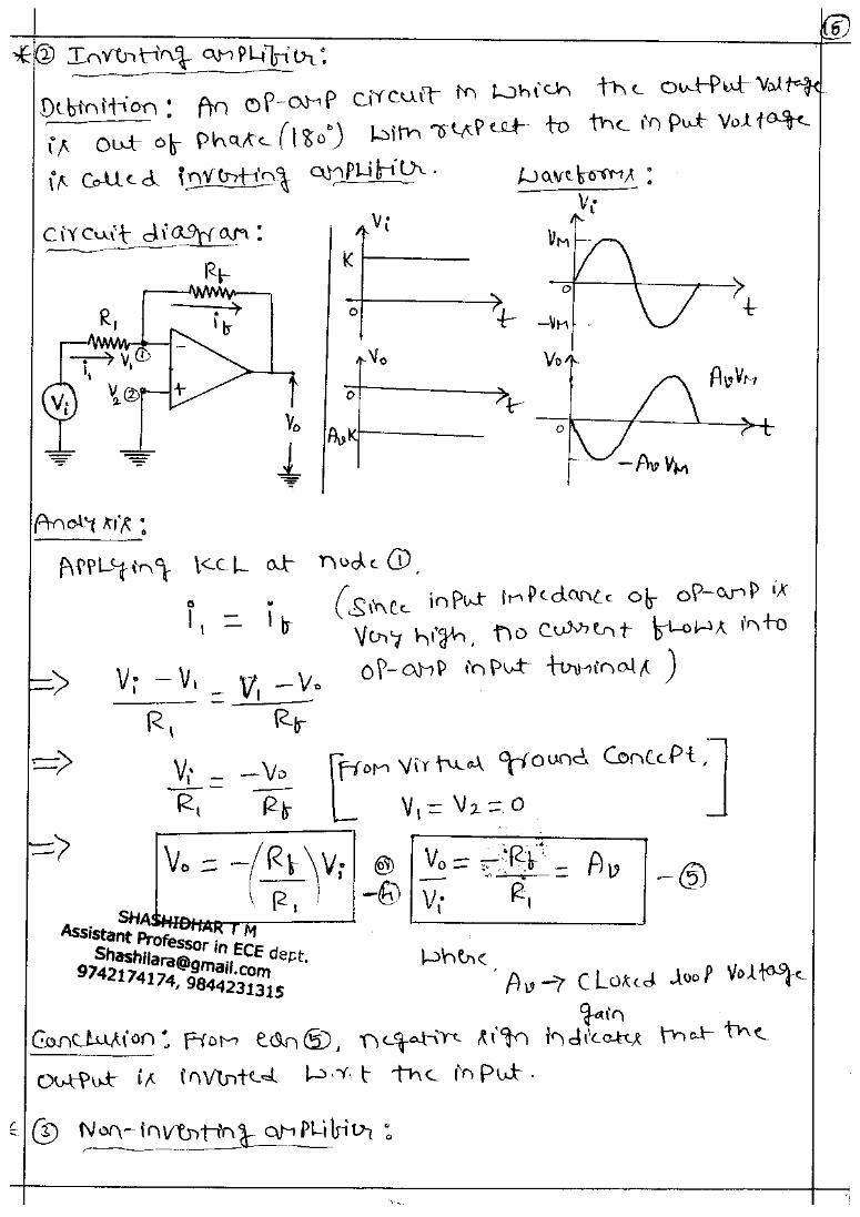
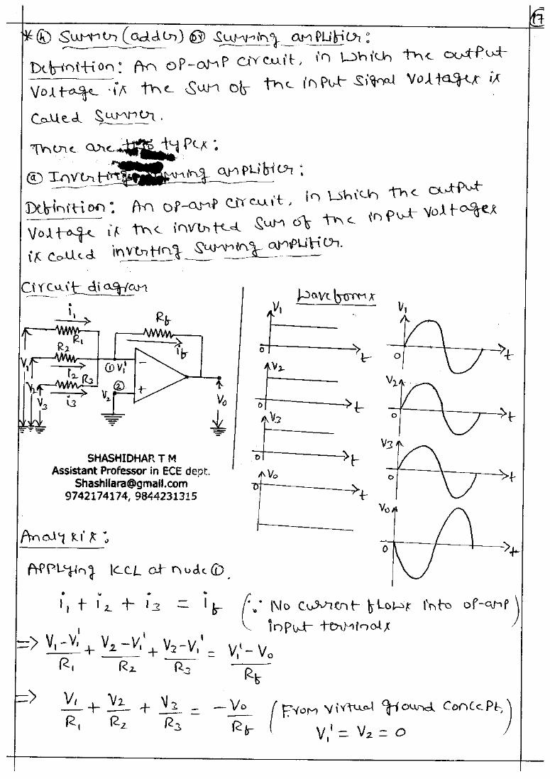
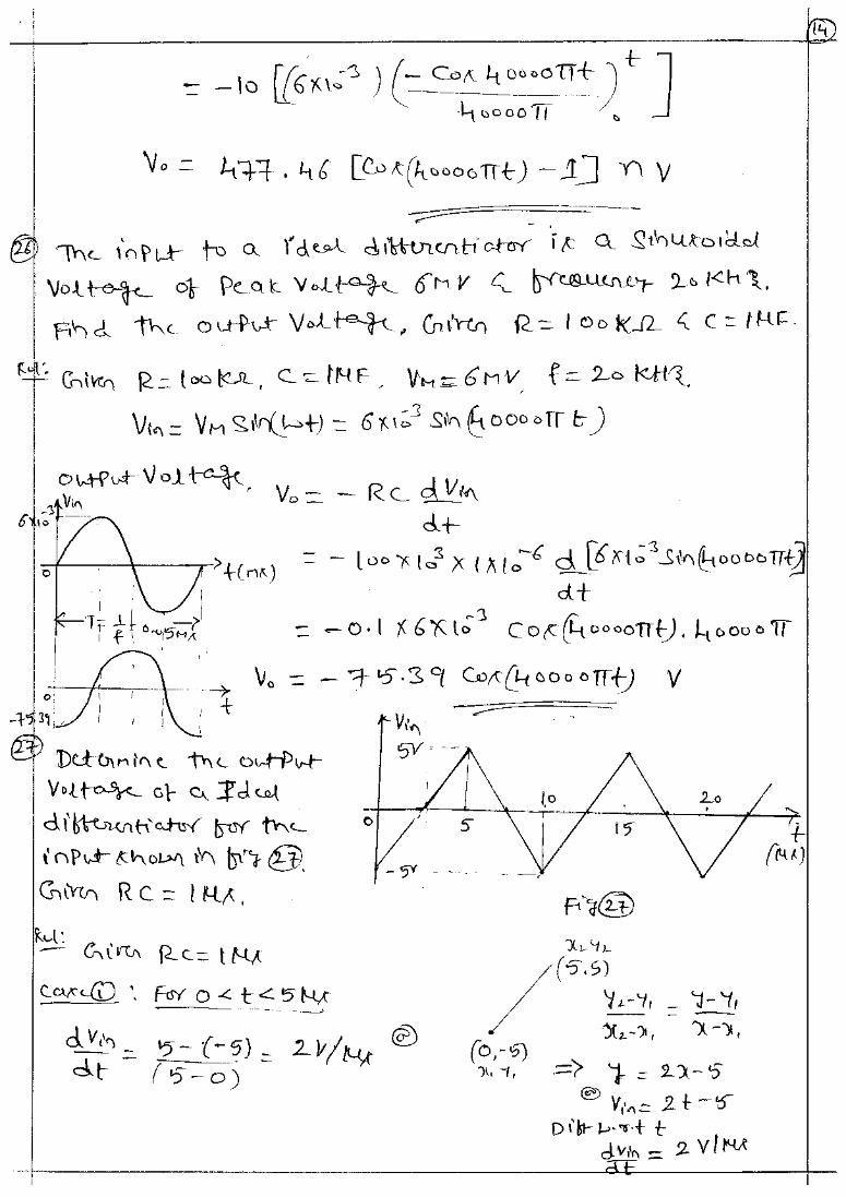
13. Explain the working of Op-Amp as: a) Inverting amplifier b) Integrator
c) Differentiator d)Voltage follower e) Non-inverting amplifier
14. List the characteristics of an ideal Op-Amp
15. Draw the transfer characteristics of an Op-amp and explain briefly.
16. Explain the need for an Op-amp.
17. List the characteristics of µA 741 Op-Amp
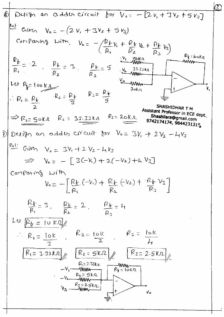
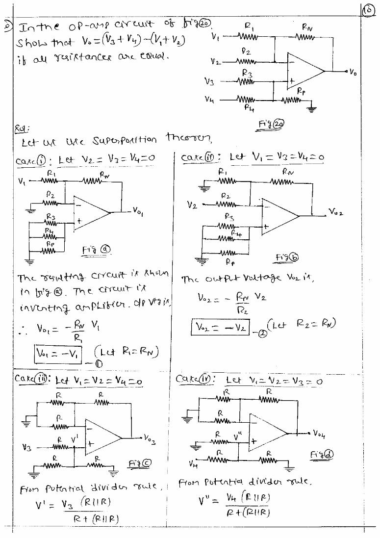
18. Derive an expression for output voltage of 3 input summing amplifier.
19. Derive an expression for output voltage of a subtractor.
Module 3: Digital Electronics
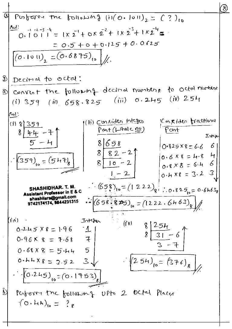
1. Convert (110.01101)2 = ( )10 and (69.25)10 = ( )2.
2. Convert (101101101)2 = ( )16 and (BAD.143)16 = ( )2
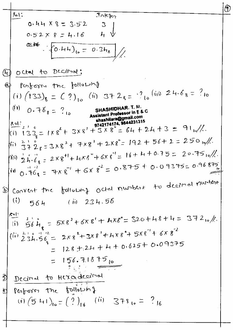
3. Convert (101.001101)2 = ( )8 and (276.045)8 = ( )2
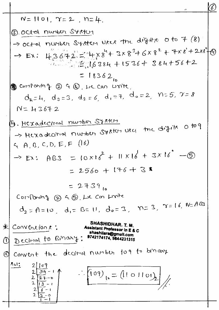
4. Convert (4567.23)8=( )10 and (678.234)10=( )8
5. Convert (54.387)10 = ( )16 and (BACE.143)16 = ( )10

SHREE PILLAPPA COLLEGE OF ENGINEERING, KONDASHETTIHALLI ROAD, BENGALURU-89 Ph no: 9742174174, 9844231315
SHASHIDHAR T M B.E (SJMIT), M.Tech (PESIT), M.Sc( Maths), (Ph.D (RVCE)) , Asst. Professor, ECE Dept.
6. Perform the following
a) (1010110.1001100101)2=(?)8=(?)10=(?)16
b) (FACE.BAC)16=(?)8=(?)10=(?)2
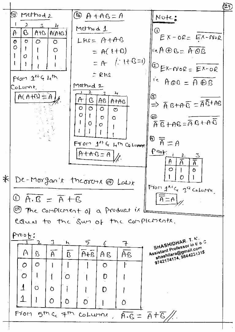
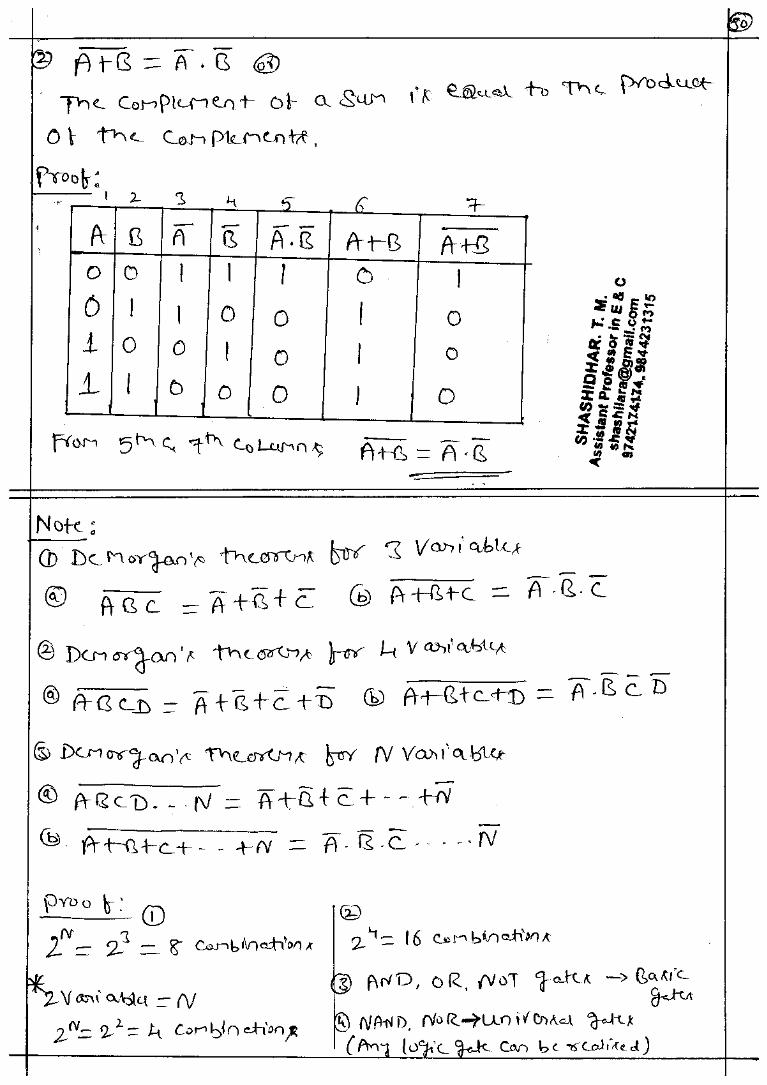
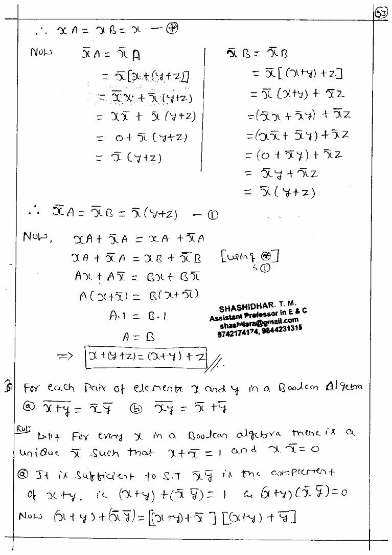
7. State and prove Demorgan’s theorems for 4 variables.
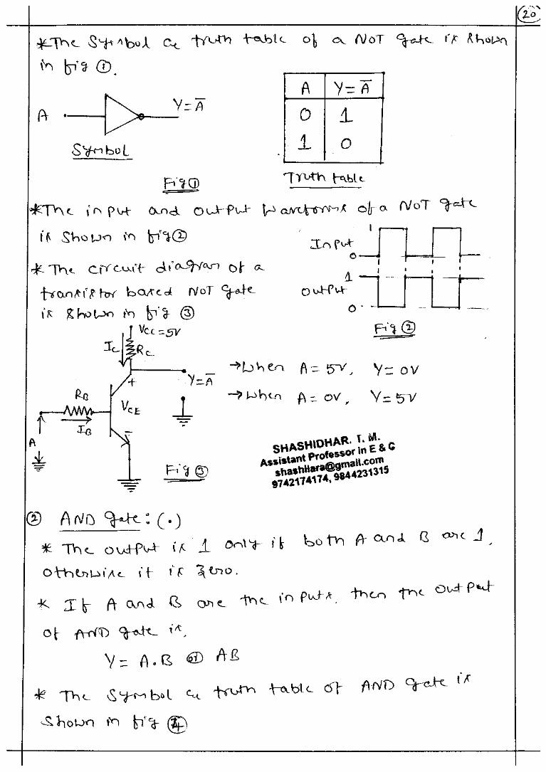
8. With a neat diagram, Explain the transistor based NOT gate.
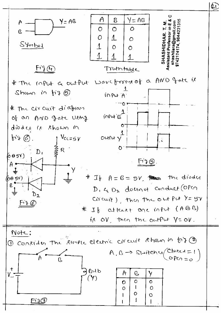
9. With a neat diagram, Explain AND and OR gates using diodes.
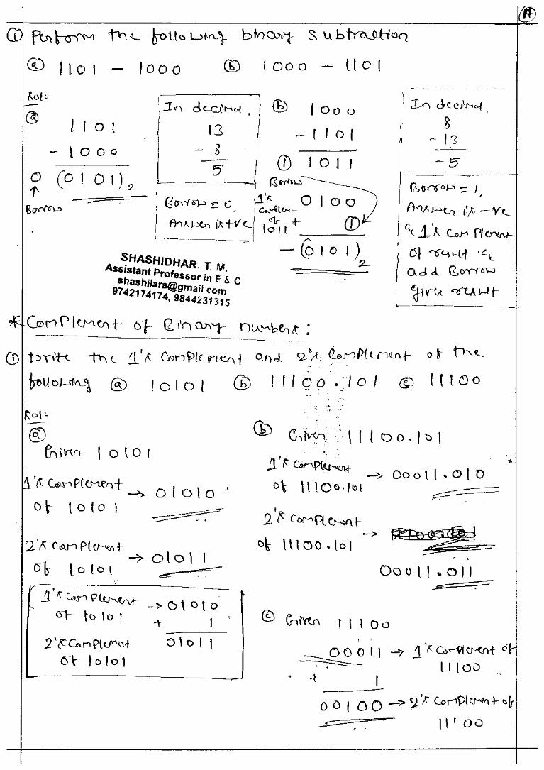
10. Write the 1’s and 2’s complement of the following a)110011 b)010101
11. Perform the following
a) (110011)2+(101011)2=(?)2 b) (101110011)2+(101111000)2=(?)2
12. Perform using 1’s and 2’s complement method
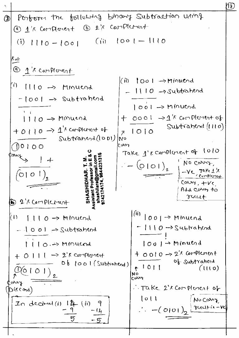
a) (101001)2-(10010)2 b) (11101)2-(10011)2 c) (98)10-(53)10
d) (567)8-(329)8 c) (ABC)16-(FED)16
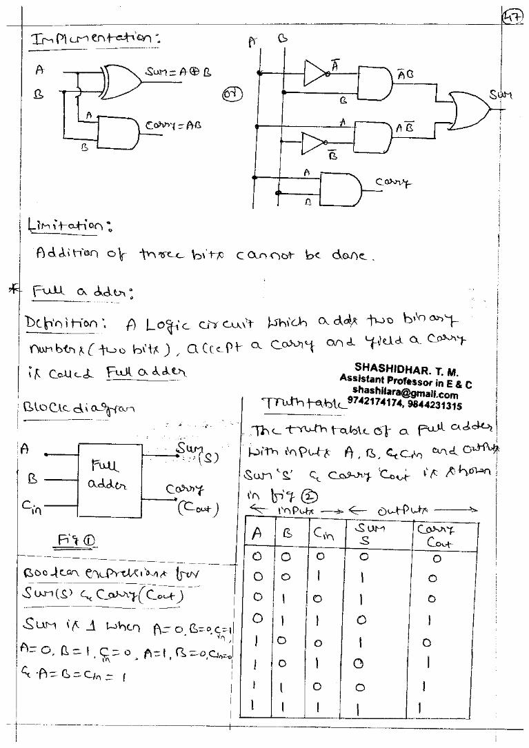
13. Realize half adder using a)NAND gates only b)NOR gates only c)Basic gates.
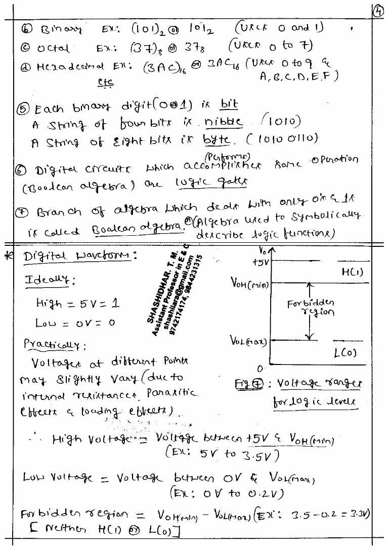
14. Compare analog and digital domains.
15. Realise Full adder using a)NAND gates only b)NOR gates only c)Basic gates.
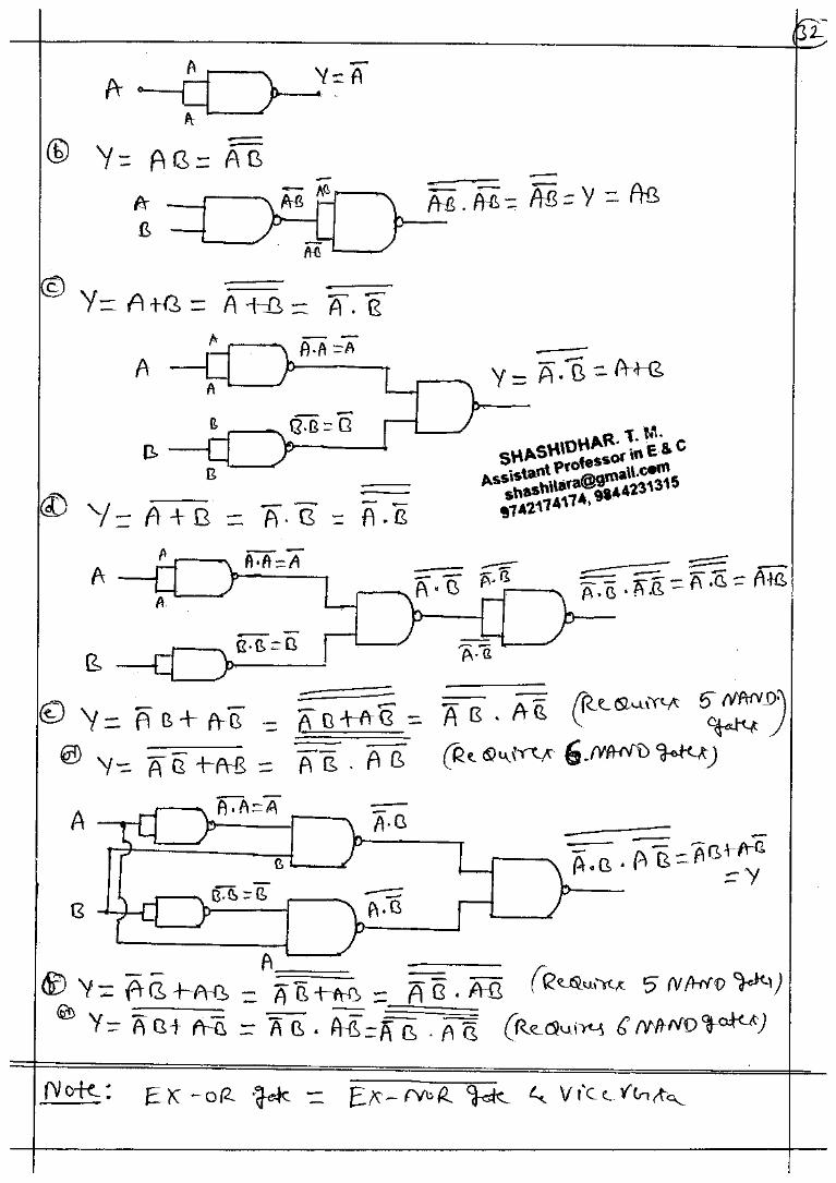
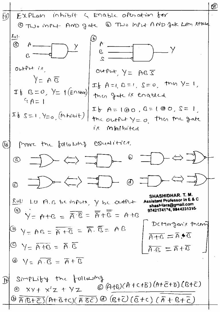
16. Implent the following gates using only NAND Gates.
a)AND b) OR c) NOT d) EX-NOR e) NOR f) EX-OR
17. Implent the following gates using only NOR Gates.
a)AND b)OR c)NOT d)EX-NOR e)NAND f)EX-OR
18. What is half Adder? Explain briefly. Also State its drawback. Suggest a
scheme to overcome it and explain briefly.
19. Explain the following gates.
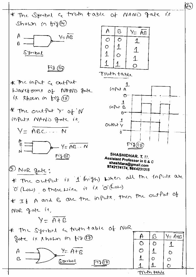
a)AND b)OR c)NOT d)XOR e)XNOR f)NAND g)NOR
20. Why NAND and NOR Gates are called Universal Gates?
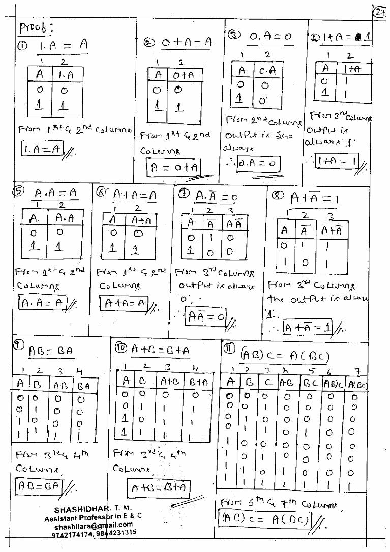
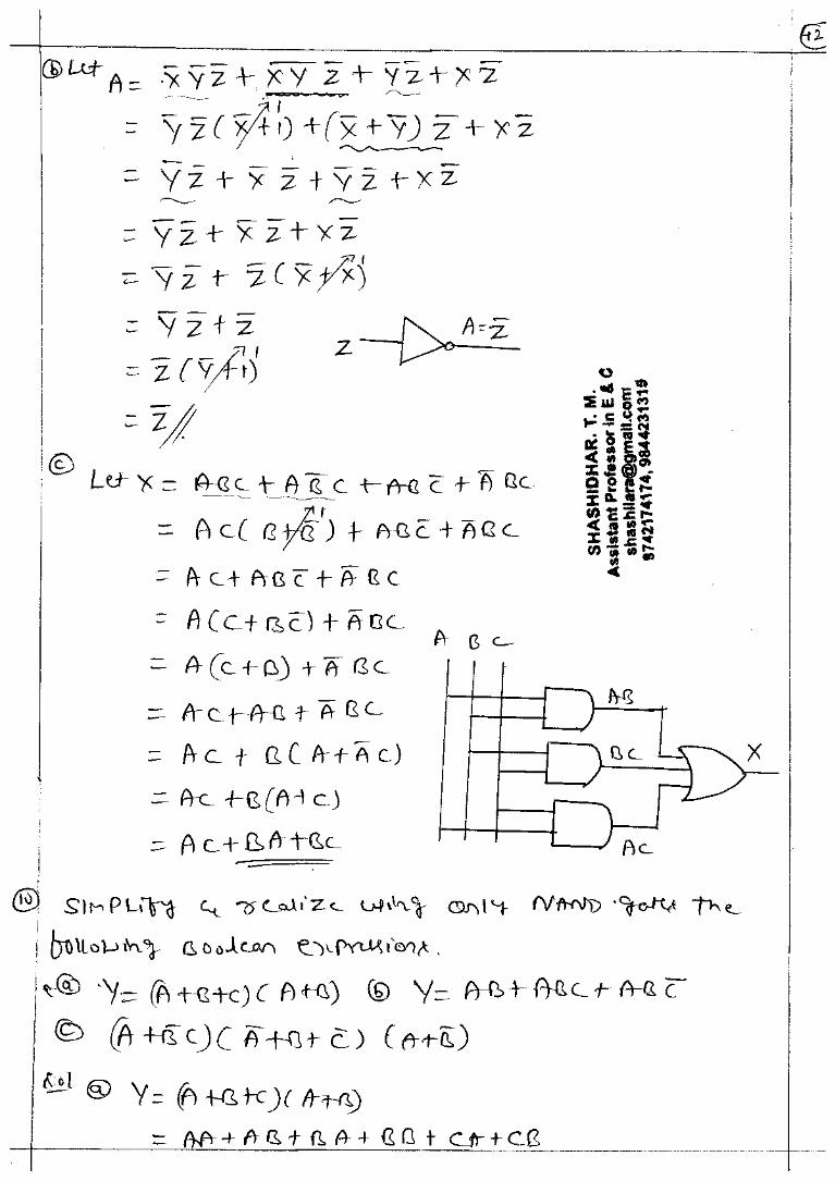
21. Prove the following Boolean expressions
a)(A+B)(A+c)=A+BC b)A(A+B)=A c)A+AB=A d)�̅�𝐵 + 𝐴�̅� = �̅��̅� + 𝐴𝐵̅̅ ̅̅ ̅̅ ̅̅ ̅̅ ̅̅
22. With truth table, circuit diagram and Boolean expressions, Explain Full
adder.
MODULE 4: a) FLIP FLOPS

SHREE PILLAPPA COLLEGE OF ENGINEERING, KONDASHETTIHALLI ROAD, BENGALURU-89 Ph no: 9742174174, 9844231315
SHASHIDHAR T M B.E (SJMIT), M.Tech (PESIT), M.Sc( Maths), (Ph.D (RVCE)) , Asst. Professor, ECE Dept.
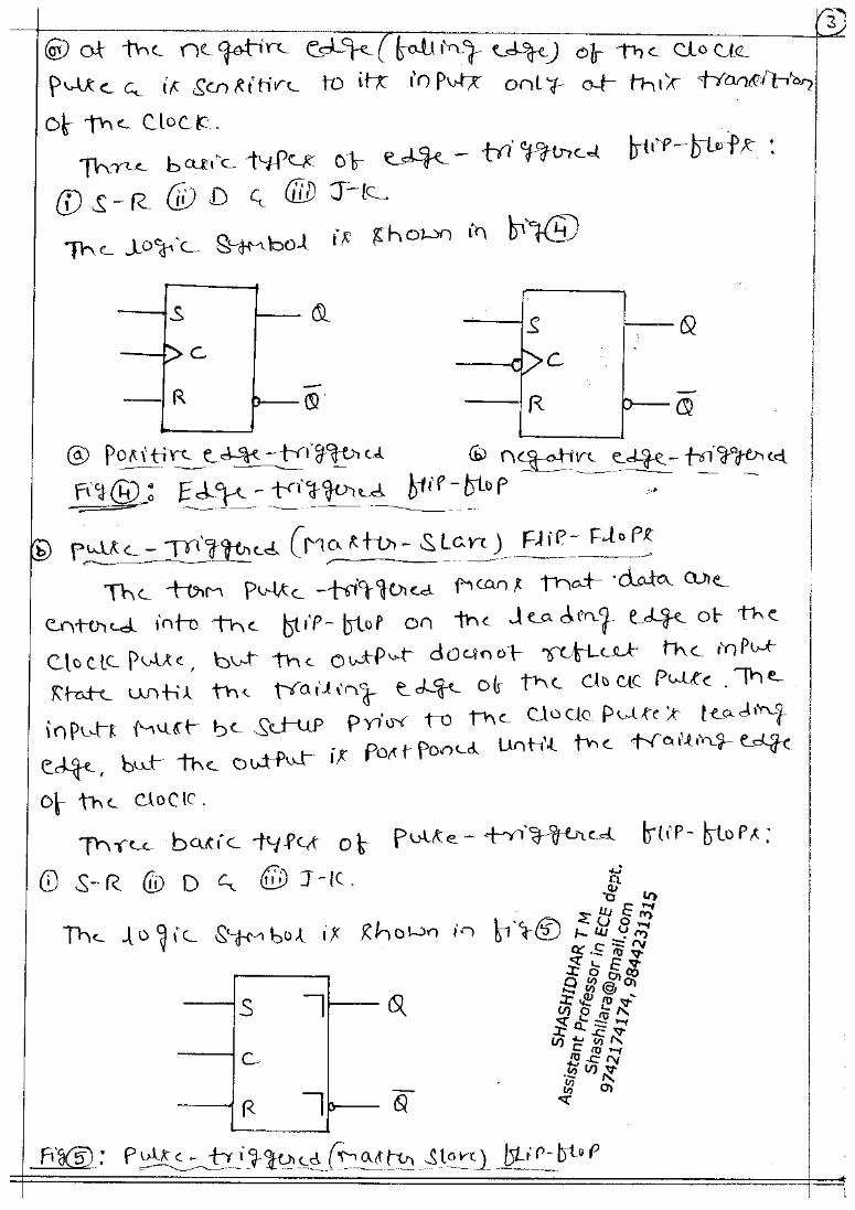
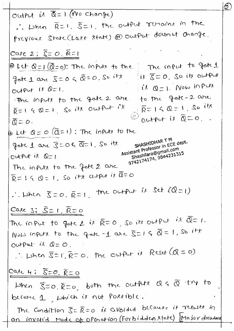
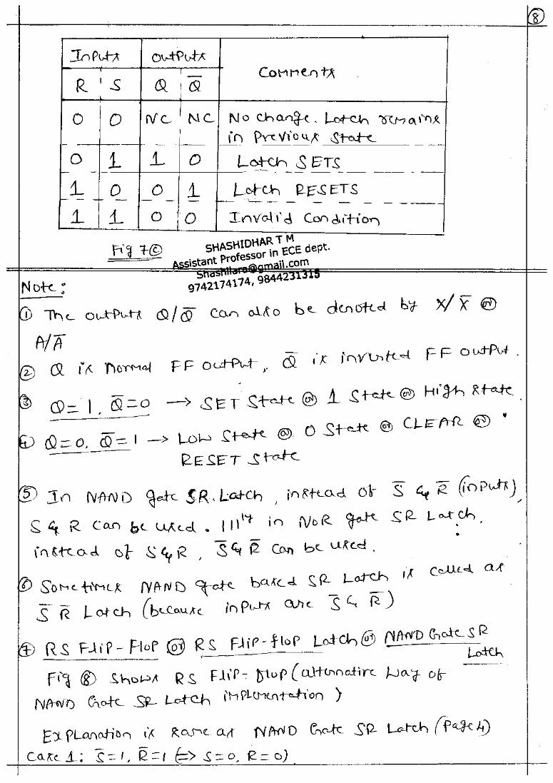
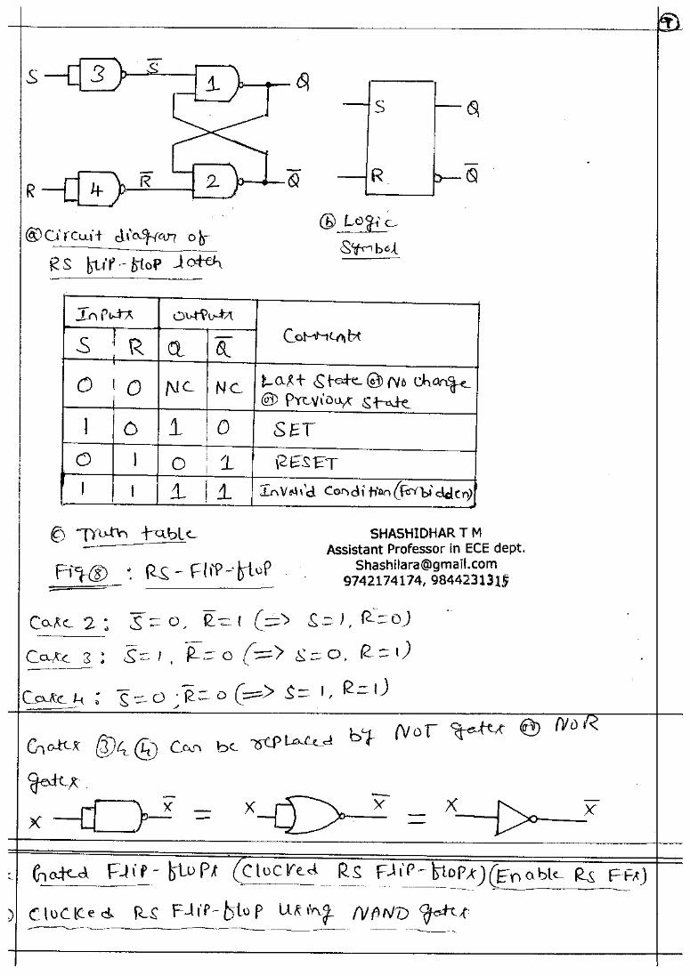
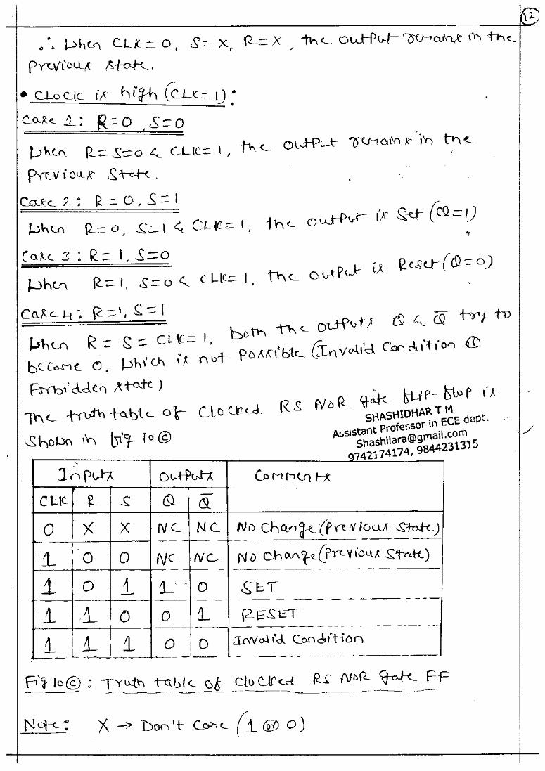
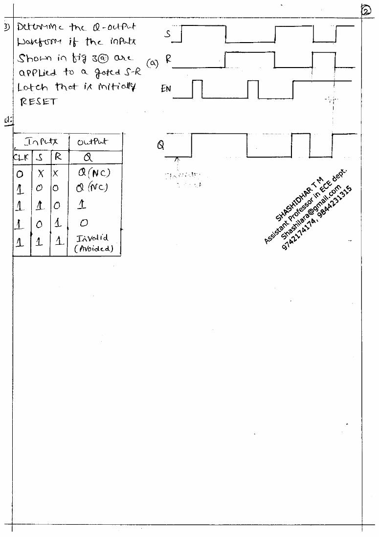
1. Write a short note on clocked RS Flip-Flop.
2. Explain the operation of NOR gate latch(NOR gate FF) using its circuit
diagram, logic symbol and truth table.
3. What is a RS Flip-Flop? Explain using its circuit diagram, logic symbol and
truth table.
4. Draw the traditional and IEEE logic symbol of AND, NOT, NOR, XOR and
XNOR.
5. What do you mean by a Flip-Flop? Explain briefly.
6. Write a short note on the categories of Flip flops.
7. List the types of Flip flops. Explain briefly anyone.
8. Give the differences between latch and flip flop.
9. With a neat circuit diagram, Logic symbol and truth table, Explain Gated
(Clocked) RS Flip-flop.
10. Explain the operation of NAND gate latch(NAND gate RS FF) using its circuit
diagram, logic symbol and truth table.
MODULE 4: b) MICROCONTROLLER
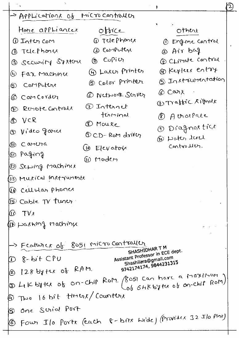
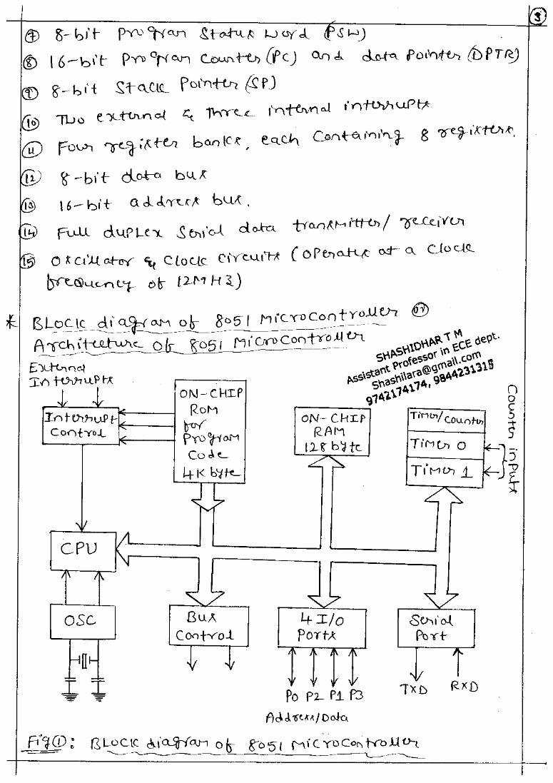
1. What is Microcontroller? List the features of µc 8051.
2. Mention the advantages of Microcontroller.
3. List the criteria for choosing a Microcontroller.
4. List the applications of Microcontroller.
5. With a neat block diagram, explain the architecture of 8051.
6. With a neat block diagram, discuss on the interfacing of stepper motor with
8051. Also write the excitation table.
7. With a neat block diagram, explain the construction details of 8051
connection to stepper motor. Write the formula to calculate step angle and
RPM of stepper motor. Also mention its advantages and applications.
MODULE 5: a) COMMUNICATION SYSTEM
1. What do you mean by modulation? Mention its types

SHREE PILLAPPA COLLEGE OF ENGINEERING, KONDASHETTIHALLI ROAD, BENGALURU-89 Ph no: 9742174174, 9844231315
SHASHIDHAR T M B.E (SJMIT), M.Tech (PESIT), M.Sc( Maths), (Ph.D (RVCE)) , Asst. Professor, ECE Dept.
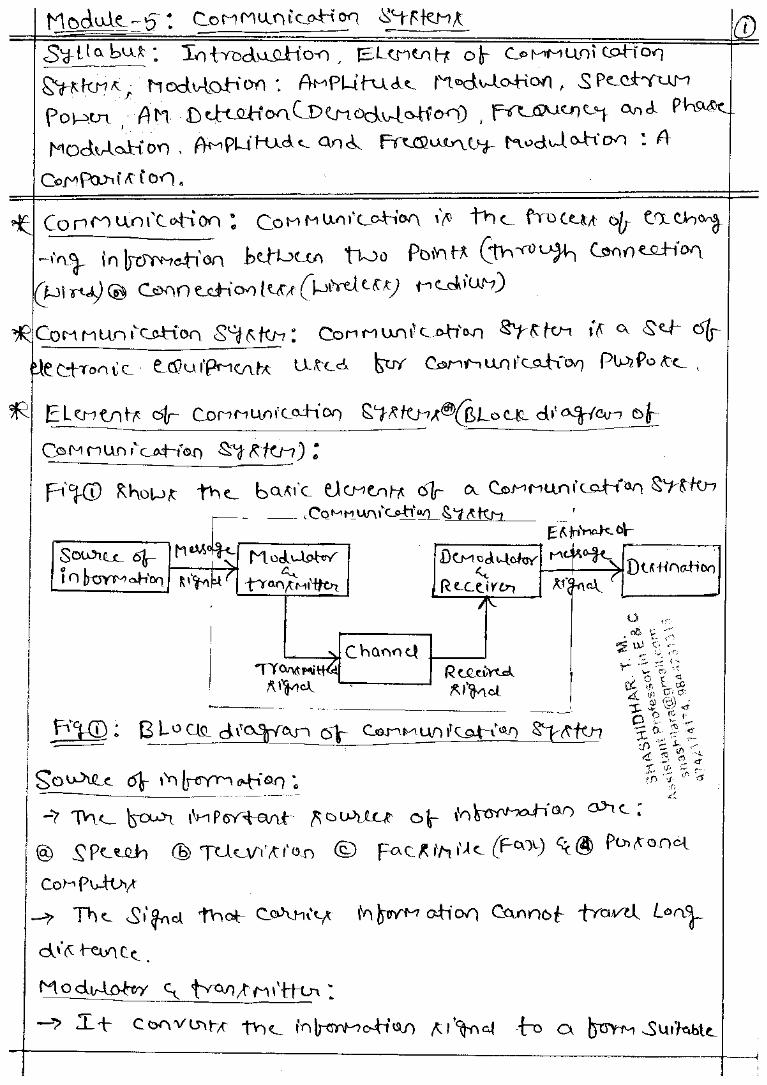
2. What do you mean by Communication ? With a neat block diagram, explain
the elements of Radio communication system.
3. Explain the necessity of modulation.
4. List out the different frequency ranges with its applications.
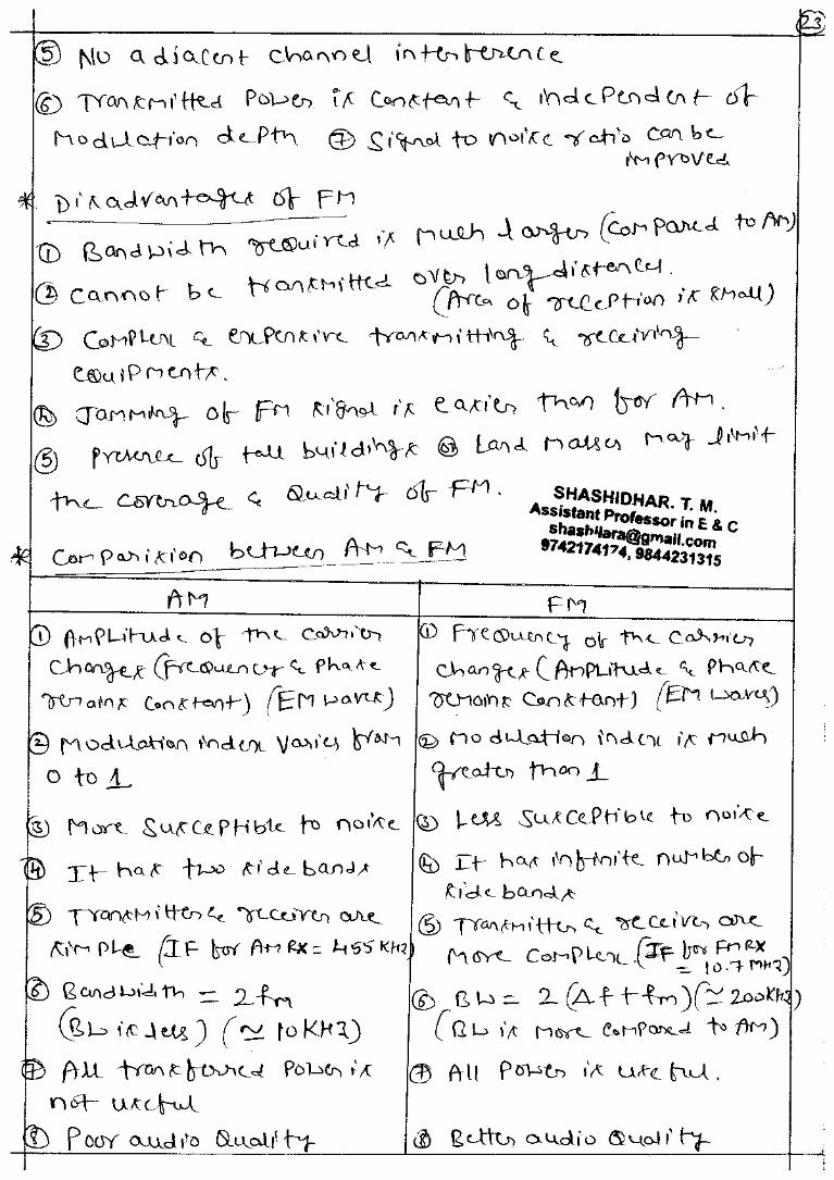
5. Compare AM, FM and PM.
6. With neat waveforms, explain the principle of Frequency Modulation. (Or)
Write a short note on FM.
7. What is angle modulation? Explain any one of the type.
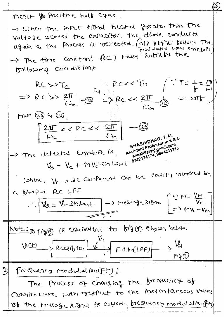
8. What is demodulation (detection)? With a neat circuit diagram and
waveforms, explain the operation of Envelope detector.
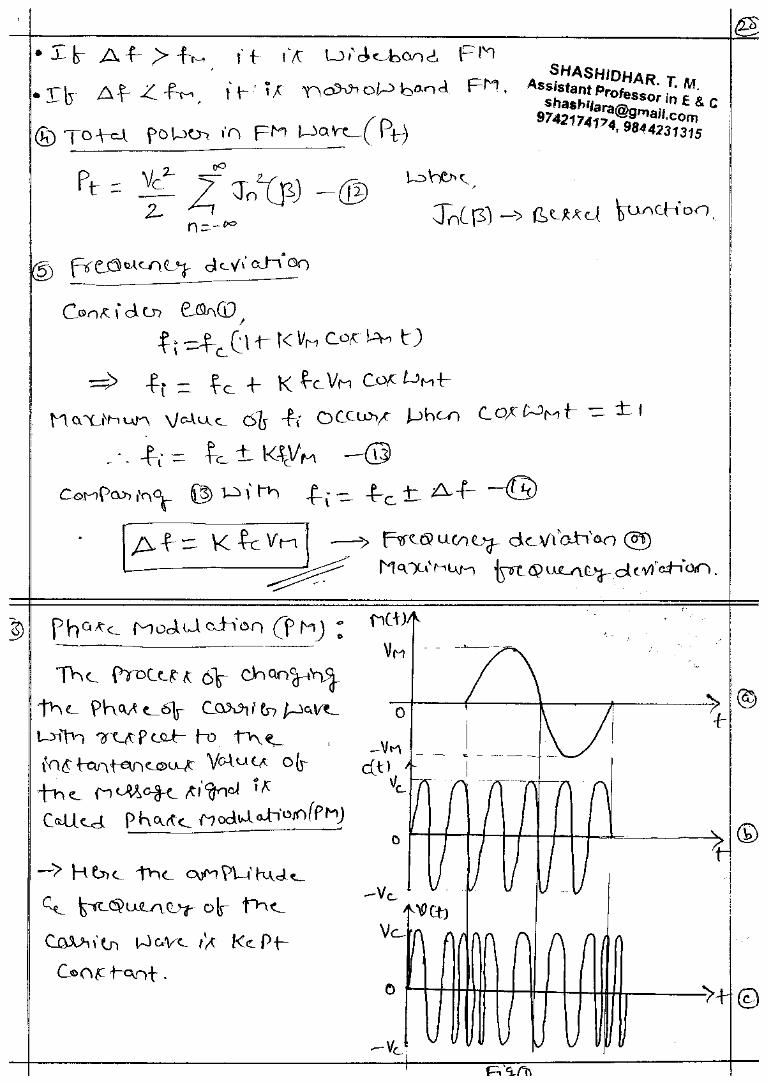
9. Derive an expression for FM wave.
10. Derive an expression for an AM wave
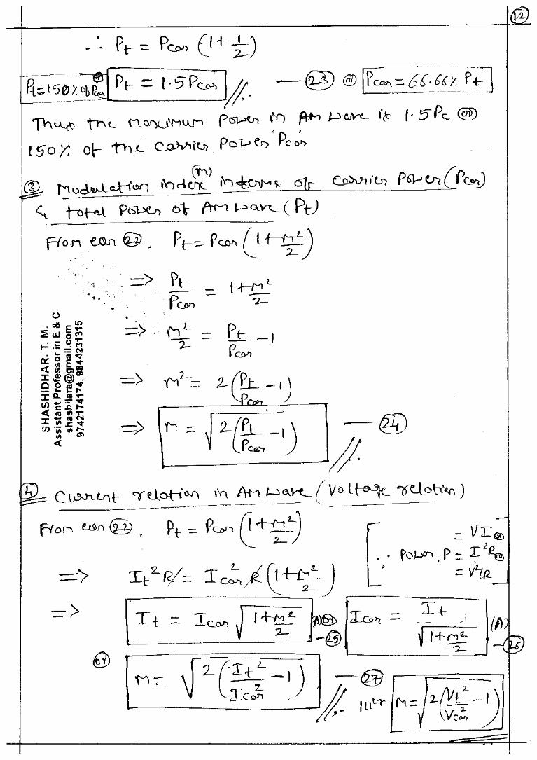
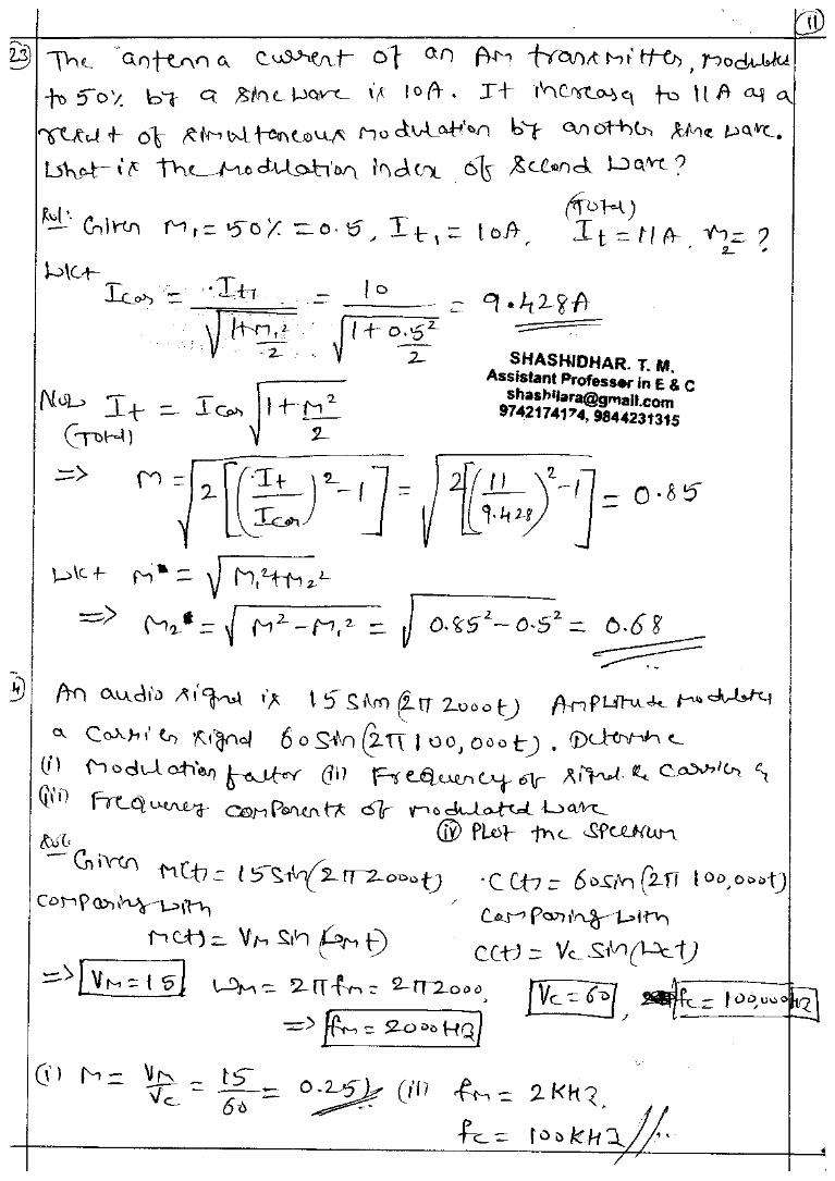
11. Derive an expression for modulation index interms of total power and carrier
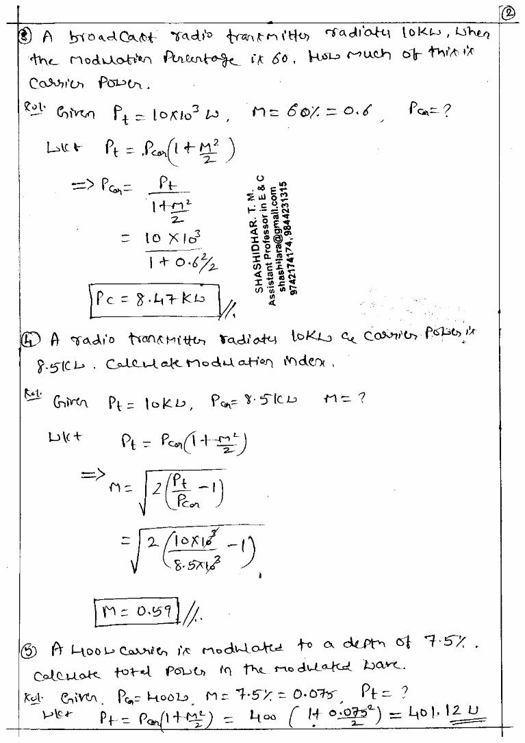
power (or total current and carrier current) of an AM wave
12. Define modulation index or depth of modulation or modulation factor. Derive
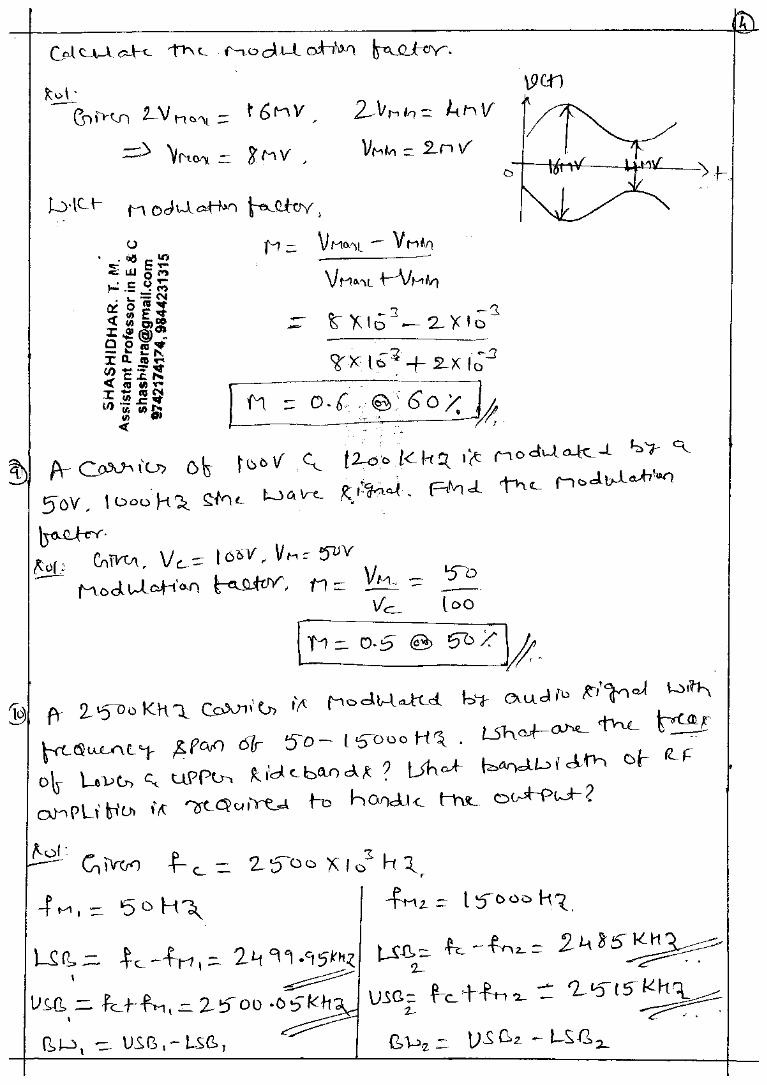
an expression for modulation index interms of maximum and minimum
voltages of AM wave.
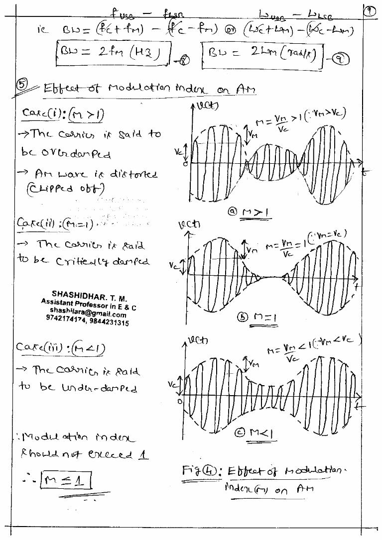
13. Explain the effect of modulation index on AM
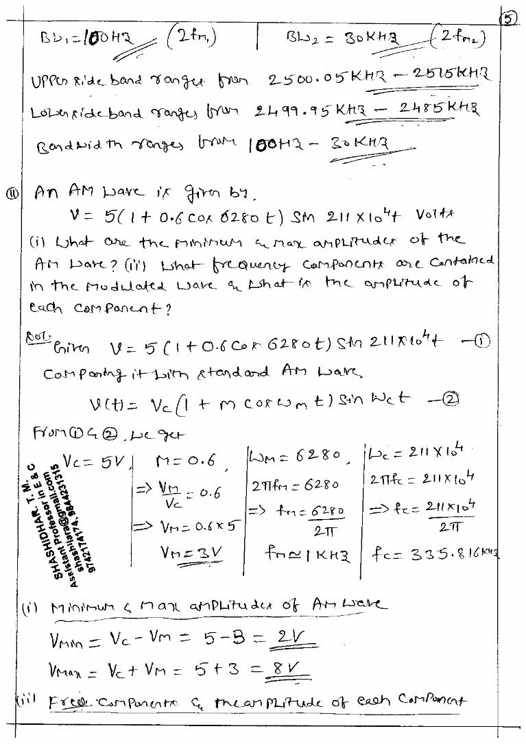
14. Draw the frequency spectrum of AM wave. Write an expression for BW of AM
wave.
15. Derive an expression for total power in an AM wave when the carrier is
modulated by N Cosine waves.
16. Derive an expression for instantaneous phase of FM wave.
17. Draw the frequency spectrum of FM wave.
18. Define the following terms w.r.t FM
i)modulation index ii)BW iii)Frequency deviation.
19. Prove that the maximum efficiency in AM is 33.33%.
20. Prove that the minimum efficiency in AM is 0%.
SHREE PILLAPPA COLLEGE OF ENGINEERING, KONDASHETTIHALLI ROAD, BENGALURU-89 Ph no: 9742174174, 9844231315
SHASHIDHAR T M B.E (SJMIT), M.Tech (PESIT), M.Sc( Maths), (Ph.D (RVCE)) , Asst. Professor, ECE Dept.
21. With a neat waveforms, explain the principle of Amplitude Modulation. (Or)
Write a short note on Amplitude modulation
22. With a neat waveforms, explain the principle of Phase Modulation with
necessary mathematical expressions.
23. With usual notations, Prove that 𝑃𝑡 =𝑉𝐶
2
2𝑅(1 +
𝑚2
2) 𝑜𝑟 𝑃𝑡 = 𝑃𝑐𝑎𝑟(1 +
𝑚2
2)
Or S T the total power in an AM wave is more than carrier power.
24. Derive an expression for total current contained in an AM wave interms of
carrier wave current and modulation index.
25. Prove that the maximum power in an AM wave is 150% of the carrier power.
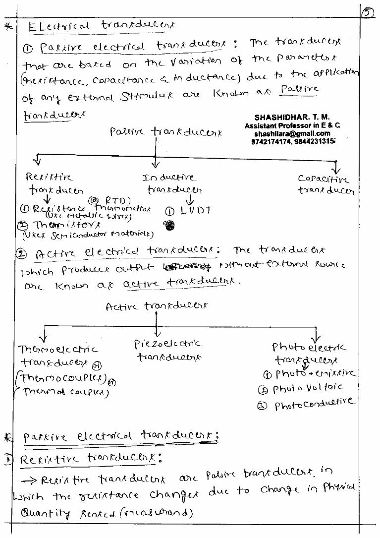
MODULE 5: b) TRANSDUCERS
1. What is transducer? Explain briefly with a neat block diagram
2. Mention the differences between Active and Passive transducers. Also list the
few measurands.
3. List the merits and demerits of electrical transducer.
4. List the Characteristics (or requirements) of a transducer.
5. Classify the transducers.
6. With a neat diagram, explain the construction and principle of operation of
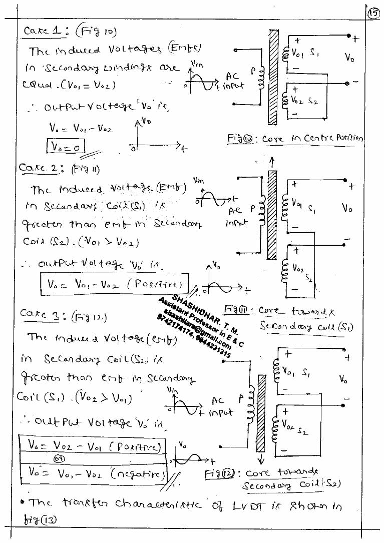
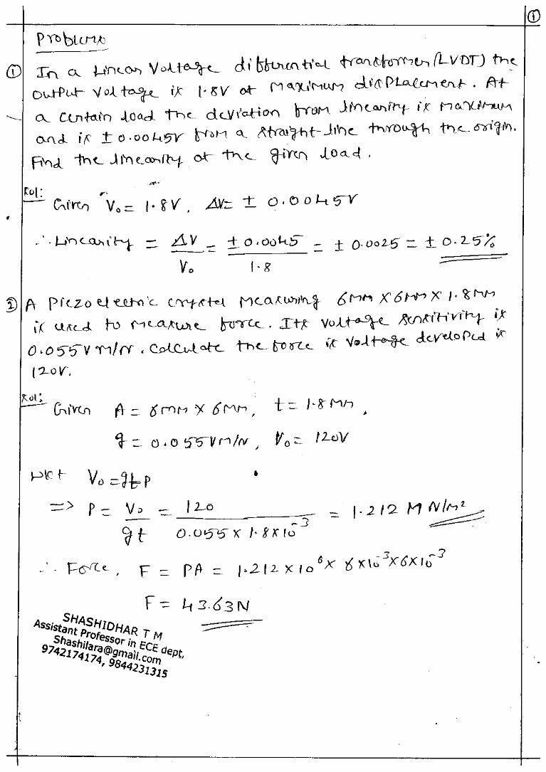
LVDT. Also state the advantages, drawbacks and applications of LVDT.
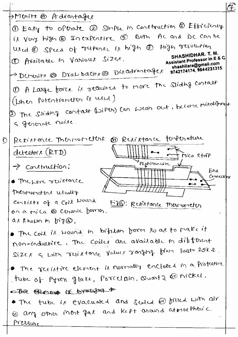
7. With a neat diagram, explain the principle of operation of Resistance
thermometer (or RTD). Also state the advantages, drawbacks and
applications of Resistance thermometer
8. With a neat diagram, explain the principle of operation of thermistor. Also
state the advantages, drawbacks and applications of thermistor.
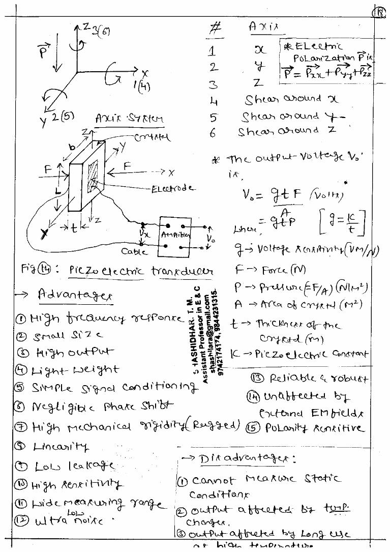
9. With a neat diagram, explain the principle of operation of Piezoelectric
transducer. Also state the advantages, drawbacks and applications of
Piezoelectric transducer.
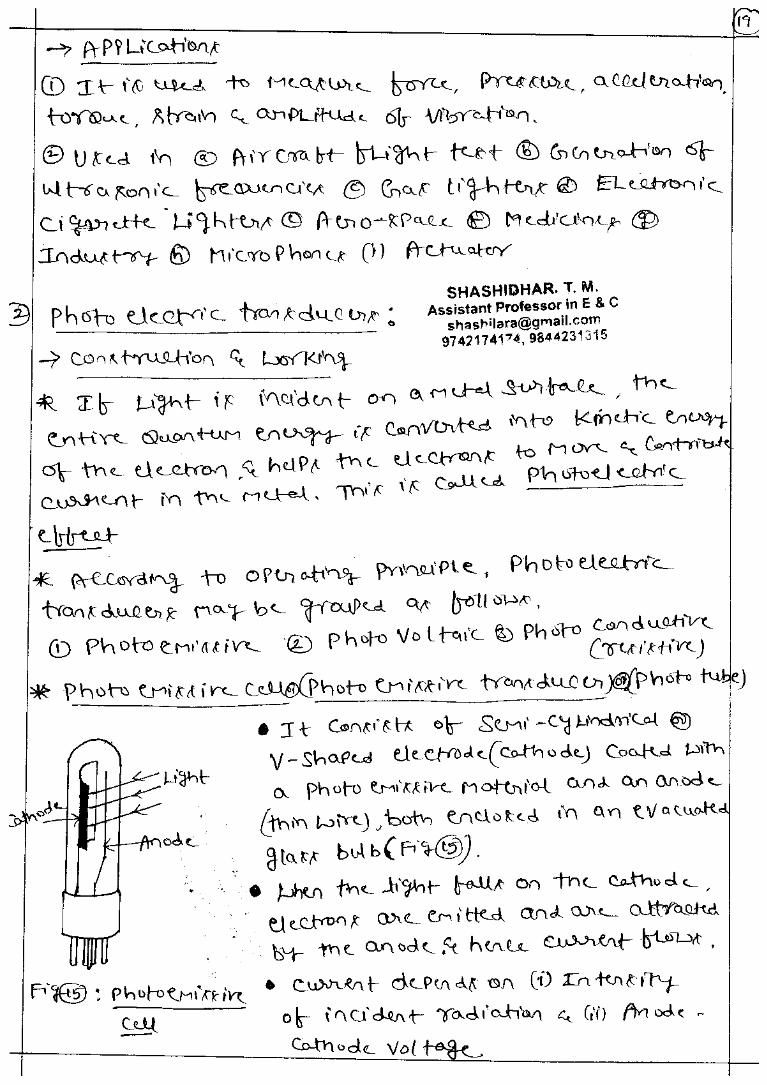
10. With a neat diagram, explain the principle of operation of Photoelectric
transducer. Also state the advantages, drawbacks and applications of
Photoelectric transducer

SHREE PILLAPPA COLLEGE OF ENGINEERING, KONDASHETTIHALLI ROAD, BENGALURU-89 Ph no: 9742174174, 9844231315
SHASHIDHAR T M B.E (SJMIT), M.Tech (PESIT), M.Sc( Maths), (Ph.D (RVCE)) , Asst. Professor, ECE Dept.
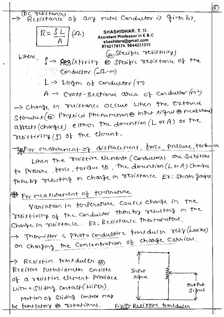
11. What do you mean by resistance transducer? Explain any one of the type.
12. What is inductive transducer? Explain briefly.
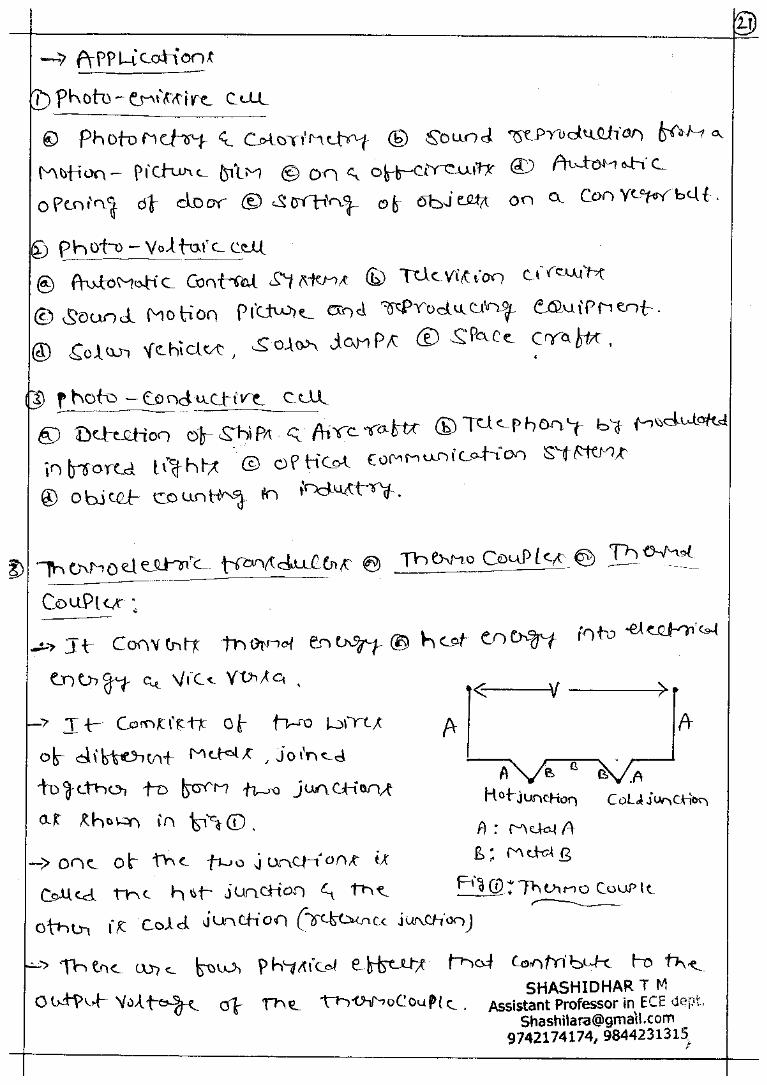
13. What is thermal couple? Explain the terms Seeback, Peltier, Thomson and
Joule effect.
14. Compare resistance thermometer and thermistor.
15. Define the following terms w.r.t resistance transducer:
a)Time Constant b) Dissipation factor c) Resistance ratio