20nmic_wp
TRANSCRIPT

Introduction
The 20nm process node promises performance, power and capacity breakthroughs that will allow electronics OEMs to provide the next generation of differentiated products. But the 20nm node also raises significant new challenges for semiconductor design and manufacturing, requiring profound changes that will range from custom/analog cell creation to digital system-on-chip (SoC) integration. The challenges, however, are manageable if EDA vendors, foundries, and IP providers work together to build 20nm-aware tools and automated flows.
Perhaps the most discussed 20nm manufacturing challenge is the need for double patterning to overcome the limits of existing lithography equipment. Double patterning has such a pervasive impact on the silicon that every step in the design flow must anticipate and prevent double patterning problems. Standard cell development, placement, clocking, routing, extraction, timing and power analysis, and design-rule checking must all be “double patterning aware.” A unified, double-patterning aware design flow across custom and digital domains is imperative.
However, 20nm challenges go far beyond double patterning. 20nm chips will typically be very complex designs with 100M gates or more, resulting in synthesis and verification challenges. Layout-dependent effects (LDE) due to lithography and stress will result in timing and power variability, causing implementation and verification challenges. Hundreds of new, complex layout and manufacturing rules will pose an implementation and signoff challenge.
From a design perspective, what is unique about 20nm is the deep and complex interdependency of manufacturing and variability, on top of increasing timing, power and area challenges. A “fix it at signoff” approach will no longer work, and must give way to a “prevent, analyze and optimize” methodology. The traditional iterative, sequential design flow is no longer adequate, because all phases of design become more interdependent at 20nm than at previous nodes.
A Call to Action: How 20nm Will Change IC Design
The 20nm process node represents a turning point for the electronics industry. While it brings tremendous power, performance and area advantages, it also comes with new challenges in such areas as lithography, variability, and complexity. The good news is that these become manageable challenges with 20nm-aware EDA tools when they are used within end-to-end, integrated design flows based on a “prevent, analyze, and optimize” methodology.
Contents
Introduction .................................1
Advantages and Costs of 20nm ...2
Silicon Manufacturability and
Variation ......................................3
Achieving “Giga Scale” Design
Productivity .................................6
Concurrent PPA Optimization .......7
Conclusion ...................................8
References ...................................8
A 20nm flow must include custom/analog as well as digital design. Nearly all 20nm systems-on-chip (SoCs) will be mixed-signal, and will integrate analog blocks. Moreover, the analog blocks will use more and more digital control circuitry, putting analog and digital circuits in ever closer proximity. Also, standard cells must be designed and characterized before digital design can commence, and these cells must follow 20nm design rules.
Only a collaborative ecosystem including EDA providers, IP suppliers, services companies, and foundries will mitigate 20nm challenges and open the door to the next generation of electronic devices. Foundry-provided process design kits (PDKs) and rule decks, foundry-qualified tool flows, and third-party IP must be in place before volume production can begin. While this article will focus on 20nm design challenges, it’s important to keep in mind that it will take deep and early collaboration throughout the semiconductor design and manufacturing ecosystem to pave the way for the 20nm electronics revolution.
Advantages and Costs of 20nm
The 20nm process node will not come cheaply. According to the research firm IBS (May 2011), 20nm fab costs will range from $4 billion to $7 billion, process R&D will range from $2.1 billion to $3 billion, design costs could range from $120 million to $500 million, and mask costs will range from $5 million to $8 million.
Despite these costs 20nm will be a compelling process node for many applications, especially in the consumer space. Early indications point to a 30-50% performance gain, 30% dynamic power savings, and 50% area reduction compared to 28nm. Chip complexity may range up to 8-12 billion transistors.
With its power, performance and area (PPA) gains, 20nm will enable a new generation of smaller, faster, more differentiated products in such areas as mobile computing, smartphones, servers, entertainment, and wireless equipment. The adoption of 20nm process technology is inevitable, and those who move early will have a competitive advantage.
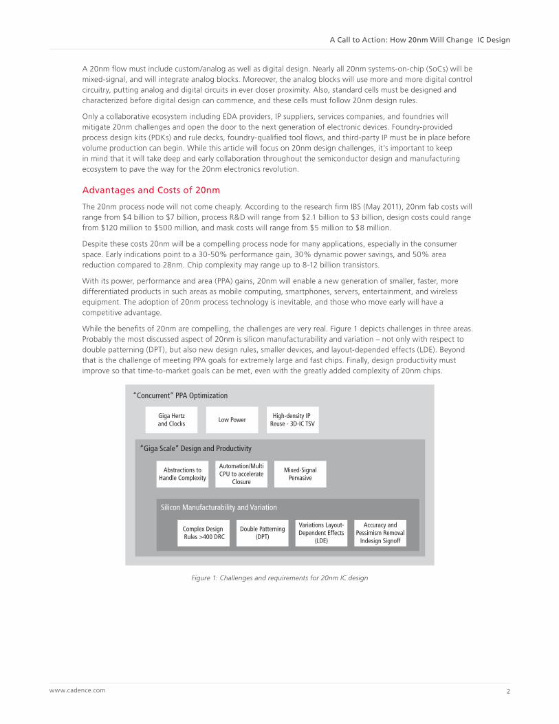
While the benefits of 20nm are compelling, the challenges are very real. Figure 1 depicts challenges in three areas. Probably the most discussed aspect of 20nm is silicon manufacturability and variation – not only with respect to double patterning (DPT), but also new design rules, smaller devices, and layout-depended effects (LDE). Beyond that is the challenge of meeting PPA goals for extremely large and fast chips. Finally, design productivity must improve so that time-to-market goals can be met, even with the greatly added complexity of 20nm chips.
“Concurrent” PPA Optimization
Giga Hertzand Clocks
Abstractions toHandle Complexity
Automation/MultiCPU to accelerate
Closure
Mixed-SignalPervasive
Low PowerHigh-density IP
Reuse - 3D-IC TSV
“Giga Scale” Design and Productivity
Complex Design Rules >400 DRC
Double Patterning(DPT)
Variations Layout-Dependent Effects
(LDE)
Accuracy andPessimism Removal
Indesign Signoff
Silicon Manufacturability and Variation
Figure 1: Challenges and requirements for 20nm IC design
www.cadence.com 2
A Call to Action: How 20nm Will Change IC Design

Silicon Manufacturability and Variation
Double patterning
While many 20nm challenges represent a worsening of phenomena already observed at higher process nodes, one challenge that’s completely new is double patterning lithography. This technology is needed to get current 193nm lithography equipment to print correctly when metal pitches are below 80nm, which will be the case for at least some of the metal layers for almost any 20nm design.
The basic idea is fairly simple. When a metal layer has design structures that are too close together to resolve with 193nm lithography, double patterning splits the layer into two separate masks. Each mask is exposed separately, and the exposures overlap to create features that are half the pitch that would otherwise be printable with 193nm lithography (Figure 2).
Conventional Lithography Double Patterning
Geometry features disappearing due to lithography distortion
Enables printing of images below minimum spacing design rules
Figure 2: Double patterning makes it possible to print features that could not be printed by conventional 193nm lithography.
Double pattering requires extra masks, along with a two-color layout decomposition process that determines how layout features will be mapped to the masks. In most cases, however, double patterning is needed only on lower metal layers.
Designers may encounter two types of double patterning, each with different design rules, advantages and tradeoffs. Litho etch litho etch (LELE) or “pitch split” is the simplest and most intuitive technique. Following layout decomposition and coloring, half the patterns go on the first mask, and half go on the second mask. With self-aligned double patterning (SADP) or “sidewall image transfer,” however, there’s a more complex process that includes depositing sidewall spacers onto relief features, removing relief features, adding dielectrics to open areas, and finally removing dielectrics everywhere except under the sidewall. The payoff is that SADP produces slightly better resolution than LELE1 (Figure 3).
Two Types of Double Patterning
Litho etch litho etch (LELE) Self-aligned double patterning (SADP)
Figure 3: Litho etch litho etch (LELE) and self-aligned double patterning (SADP)
provide alternative approaches to double patterning.
www.cadence.com 3
A Call to Action: How 20nm Will Change IC Design
Double patterning impacts every part of the IC design phase, from standard cell development to placement, routing, extraction, and physical verification. It requires a correct-by-construction methodology in which every tool is double-patterning aware, and in-design signoff makes a lengthy final signoff process unnecessary. More specifically, double patterning places these requirements on design tools:
• Cell and library generation must ensure that cells and IP blocks are compliant with double patterning design rules. These rules impose tip-to-tip, tip-to-side, side-to-side, and corner-to-corner restrictions on cell layout.
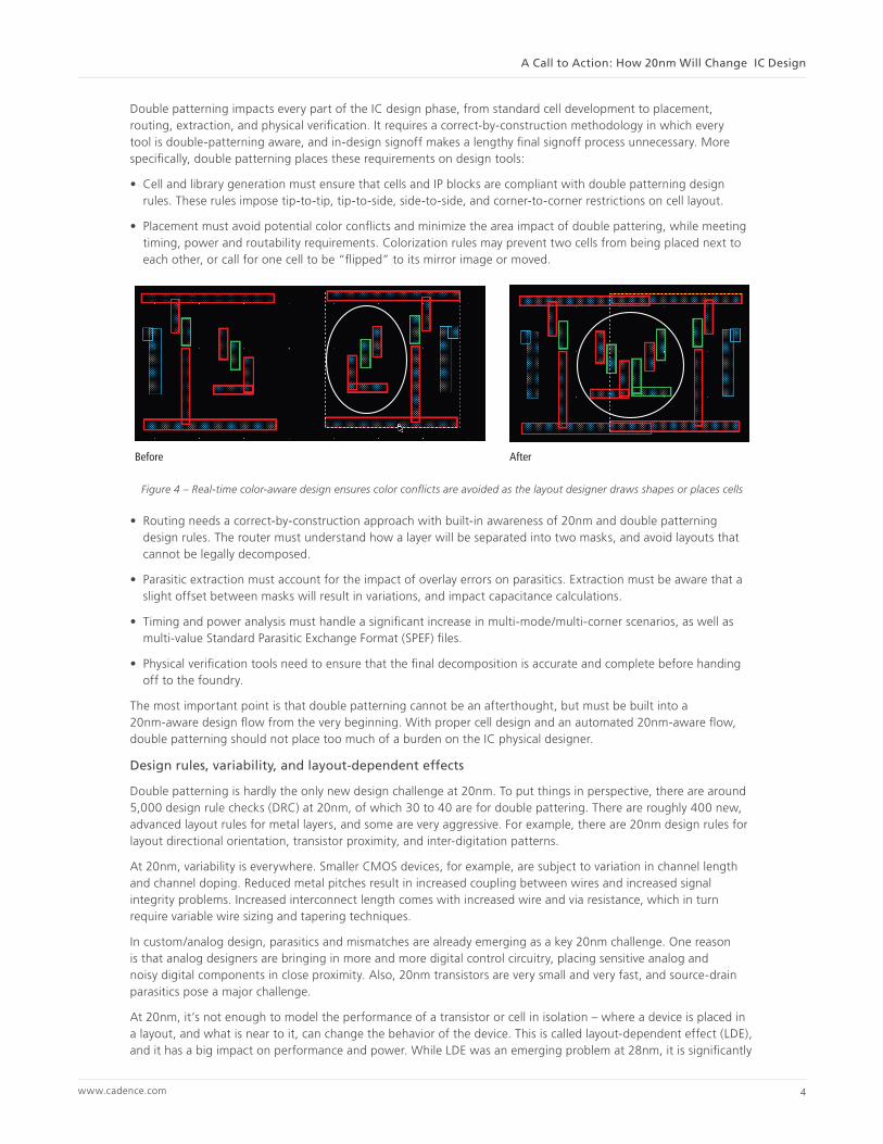
• Placement must avoid potential color conflicts and minimize the area impact of double pattering, while meeting timing, power and routability requirements. Colorization rules may prevent two cells from being placed next to each other, or call for one cell to be “flipped” to its mirror image or moved.
Before After
Figure 4 – Real-time color-aware design ensures color conflicts are avoided as the layout designer draws shapes or places cells
• Routing needs a correct-by-construction approach with built-in awareness of 20nm and double patterning design rules. The router must understand how a layer will be separated into two masks, and avoid layouts that cannot be legally decomposed.
• Parasitic extraction must account for the impact of overlay errors on parasitics. Extraction must be aware that a slight offset between masks will result in variations, and impact capacitance calculations.
• Timing and power analysis must handle a significant increase in multi-mode/multi-corner scenarios, as well as multi-value Standard Parasitic Exchange Format (SPEF) files.
• Physical verification tools need to ensure that the final decomposition is accurate and complete before handing off to the foundry.
The most important point is that double patterning cannot be an afterthought, but must be built into a 20nm-aware design flow from the very beginning. With proper cell design and an automated 20nm-aware flow, double patterning should not place too much of a burden on the IC physical designer.
Design rules, variability, and layout-dependent effects
Double patterning is hardly the only new design challenge at 20nm. To put things in perspective, there are around 5,000 design rule checks (DRC) at 20nm, of which 30 to 40 are for double pattering. There are roughly 400 new, advanced layout rules for metal layers, and some are very aggressive. For example, there are 20nm design rules for layout directional orientation, transistor proximity, and inter-digitation patterns.
At 20nm, variability is everywhere. Smaller CMOS devices, for example, are subject to variation in channel length and channel doping. Reduced metal pitches result in increased coupling between wires and increased signal integrity problems. Increased interconnect length comes with increased wire and via resistance, which in turn require variable wire sizing and tapering techniques.
In custom/analog design, parasitics and mismatches are already emerging as a key 20nm challenge. One reason is that analog designers are bringing in more and more digital control circuitry, placing sensitive analog and noisy digital components in close proximity. Also, 20nm transistors are very small and very fast, and source-drain parasitics pose a major challenge.
At 20nm, it’s not enough to model the performance of a transistor or cell in isolation – where a device is placed in a layout, and what is near to it, can change the behavior of the device. This is called layout-dependent effect (LDE), and it has a big impact on performance and power. While LDE was an emerging problem at 28nm, it is significantly
www.cadence.com 4
A Call to Action: How 20nm Will Change IC Design
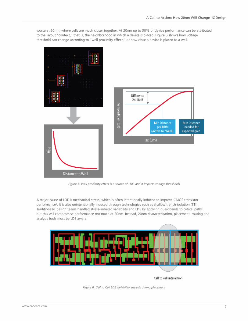
worse at 20nm, where cells are much closer together. At 20nm up to 30% of device performance can be attributed to the layout “context,” that is, the neighborhood in which a device is placed. Figure 5 shows how voltage threshold can change according to “well proximity effect,” or how close a device is placed to a well.
V TH
Distance to Well
sc (um)
Sampled G
ain (dB)
Min Distanceper DRM
(Active to NWell)
Min Distanceneeded for
expected gain
Difference24.18dB
Figure 5: Well proximity effect is a source of LDE, and it impacts voltage thresholds
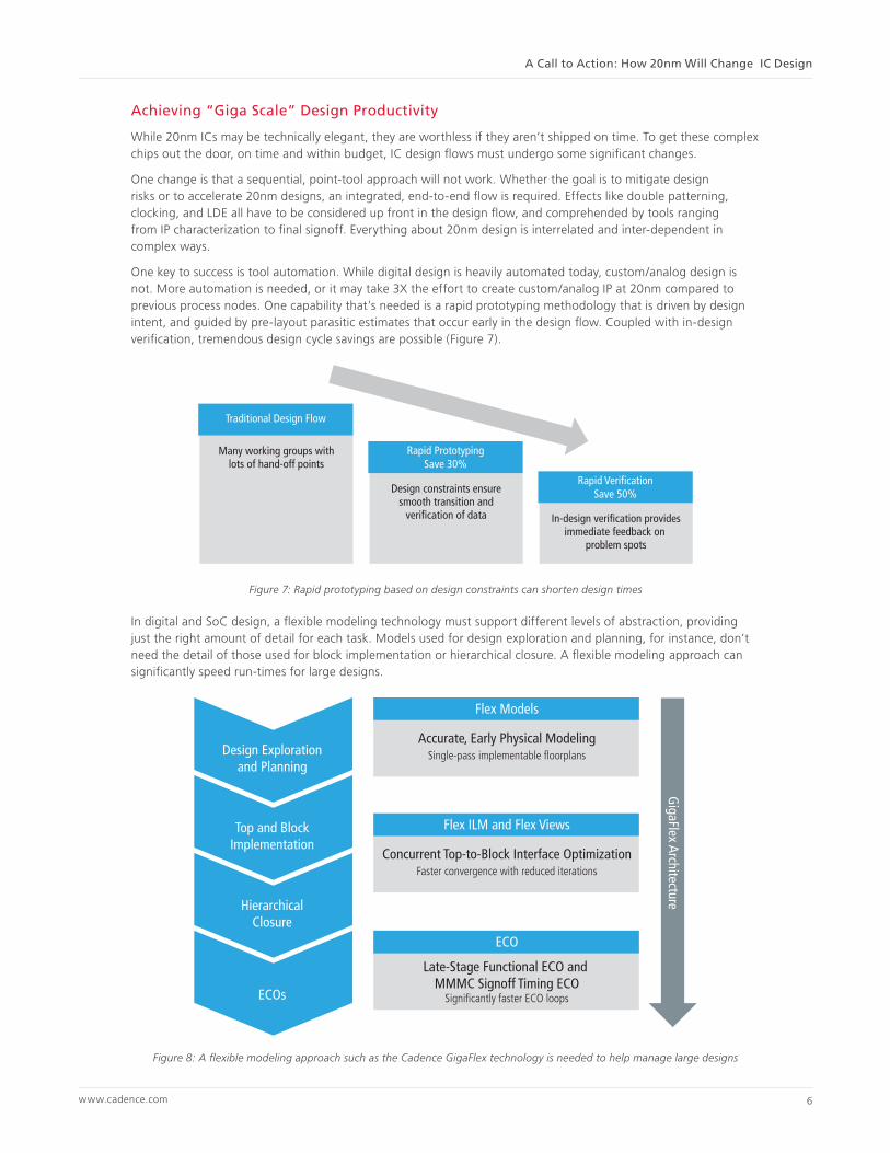
A major cause of LDE is mechanical stress, which is often intentionally induced to improve CMOS transistor performance2. It is also unintentionally induced through technologies such as shallow trench isolation (STI). Traditionally, design teams handled stress-induced variability and LDE by applying guardbands to critical paths, but this will compromise performance too much at 20nm. Instead, 20nm characterization, placement, routing and analysis tools must be LDE aware.
Cell to cell interaction
Figure 6: Cell to Cell LDE variability analysis during placement
www.cadence.com 5
A Call to Action: How 20nm Will Change IC Design
Achieving “Giga Scale” Design Productivity
While 20nm ICs may be technically elegant, they are worthless if they aren’t shipped on time. To get these complex chips out the door, on time and within budget, IC design flows must undergo some significant changes.
One change is that a sequential, point-tool approach will not work. Whether the goal is to mitigate design risks or to accelerate 20nm designs, an integrated, end-to-end flow is required. Effects like double patterning, clocking, and LDE all have to be considered up front in the design flow, and comprehended by tools ranging from IP characterization to final signoff. Everything about 20nm design is interrelated and inter-dependent in complex ways.
One key to success is tool automation. While digital design is heavily automated today, custom/analog design is not. More automation is needed, or it may take 3X the effort to create custom/analog IP at 20nm compared to previous process nodes. One capability that’s needed is a rapid prototyping methodology that is driven by design intent, and guided by pre-layout parasitic estimates that occur early in the design flow. Coupled with in-design verification, tremendous design cycle savings are possible (Figure 7).
Traditional Design Flow
Many working groups withlots of hand-off points
Rapid PrototypingSave 30%
Design constraints ensuresmooth transition and
verification of data
Rapid VerificationSave 50%
In-design verification providesimmediate feedback on
problem spots
Figure 7: Rapid prototyping based on design constraints can shorten design times
In digital and SoC design, a flexible modeling technology must support different levels of abstraction, providing just the right amount of detail for each task. Models used for design exploration and planning, for instance, don’t need the detail of those used for block implementation or hierarchical closure. A flexible modeling approach can significantly speed run-times for large designs.
Design Explorationand Planning
Top and BlockImplementation
HierarchicalClosure
ECOs
Flex Models
Accurate, Early Physical ModelingSingle-pass implementable floorplans
Flex ILM and Flex Views
Concurrent Top-to-Block Interface OptimizationFaster convergence with reduced iterations
ECO
Late-Stage Functional ECO and MMMC Signoff Timing ECO
Significantly faster ECO loops
GigaFlex Architecture
Figure 8: A flexible modeling approach such as the Cadence GigaFlex technology is needed to help manage large designs
www.cadence.com 6
A Call to Action: How 20nm Will Change IC Design
Finally, a correct-by-design approach is critical, and it calls for in-design signoff throughout the design flow. In this approach, “signoff quality” engines for placement, routing, design for manufacturability (DFM), and timing and signal integrity analysis (among others) check the work that’s been done before moving on. If everything is left to a final signoff verification run, error will compound upon error, leaving a design that is likely to be unfixable.
The approach that can avoid “unfixable” designs is “Prevent, Analyze and Optimize.” This approach must drive both custom and digital platforms to enable faster, convergent design closure solutions for advanced nodes. Many errors can be prevented with a constraint-driven design environment, LDE-aware placement, color-aware placement and routing, and in-design verification. Analysis must handle the dozens of corners that designers will face at 20nm, and do so quickly. With prevention and analysis, the optimization step is easy with relatively few errors to fix. There will always be ECOs, but they can be handled quickly and efficiently.
Concurrent PPA Optimization
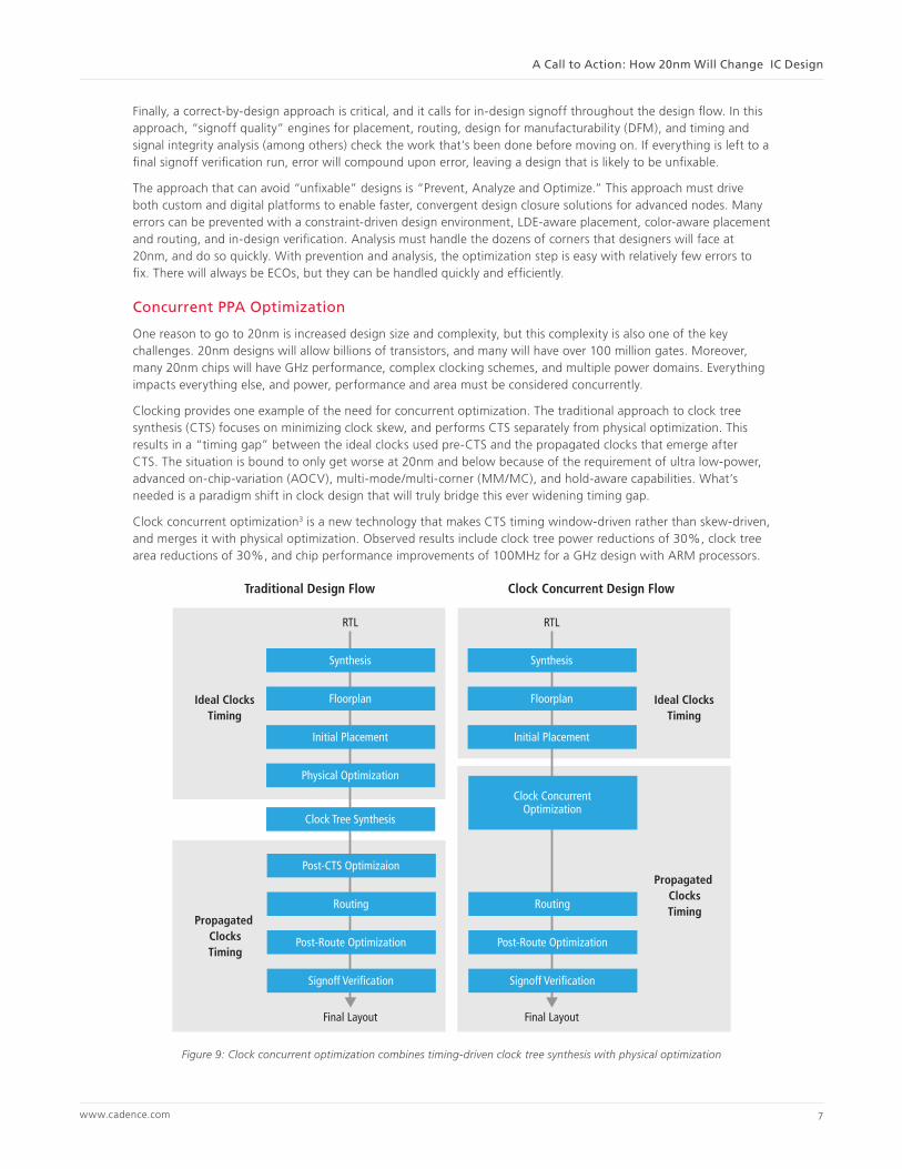
One reason to go to 20nm is increased design size and complexity, but this complexity is also one of the key challenges. 20nm designs will allow billions of transistors, and many will have over 100 million gates. Moreover, many 20nm chips will have GHz performance, complex clocking schemes, and multiple power domains. Everything impacts everything else, and power, performance and area must be considered concurrently.
Clocking provides one example of the need for concurrent optimization. The traditional approach to clock tree synthesis (CTS) focuses on minimizing clock skew, and performs CTS separately from physical optimization. This results in a “timing gap” between the ideal clocks used pre-CTS and the propagated clocks that emerge after CTS. The situation is bound to only get worse at 20nm and below because of the requirement of ultra low-power, advanced on-chip-variation (AOCV), multi-mode/multi-corner (MM/MC), and hold-aware capabilities. What’s needed is a paradigm shift in clock design that will truly bridge this ever widening timing gap.
Clock concurrent optimization3 is a new technology that makes CTS timing window-driven rather than skew-driven, and merges it with physical optimization. Observed results include clock tree power reductions of 30%, clock tree area reductions of 30%, and chip performance improvements of 100MHz for a GHz design with ARM processors.
Synthesis
RTL
Final Layout
Ideal ClocksTiming
Traditional Design Flow Clock Concurrent Design Flow
Floorplan
Initial Placement
Physical Optimization
Clock Tree Synthesis
Post-CTS Optimizaion
Propagated ClocksTiming
Routing
Post-Route Optimization
Signoff Verification
Synthesis
RTL
Final Layout
Ideal ClocksTiming
Floorplan
Initial Placement
Clock ConcurrentOptimization
Propagated ClocksTiming
Routing
Post-Route Optimization
Signoff Verification
Figure 9: Clock concurrent optimization combines timing-driven clock tree synthesis with physical optimization
www.cadence.com 7
A Call to Action: How 20nm Will Change IC Design
To deal with the large sizes of 20nm ICs, SoC design teams will integrate and verify large amounts of pre-existing analog and digital IP blocks. Even at 80% reuse, however, there will be a lot of new circuitry to design and verify. There will be no alternative to using higher levels of abstraction for both design and verification, along with tools that are high-capacity, high-speed, and heavily automated.
In the consumer market, 20nm chips must be both high performance and low power, adding to complexity and forcing difficult tradeoffs. Many 20nm chips will use advanced power management techniques such as multiple voltage islands and power shutoff. These different modes of operation will add to the verification burden. Power and signal integrity management will also be needed across chips, packages and boards, making IC/package co-design more important than ever.
Eventually, we can expect that many 20nm dies will go into 2.5D (silicon interposer) and 3D (stacked die with through-silicon via) packages. Many stacked-die implementations will include both analog and digital dies. A 3D-aware digital flow, a custom/analog flow, and a strong IC/package co-design capability will be needed to make stacked die feasible and cost-effective4.
Conclusion
As we have seen, 20nm poses many challenges for design teams, but these challenges are manageable with the right tools and methodologies. And while 20nm will call for new approaches to IC design and manufacturability, the changes will result in overall improvements to the IC design flow.
For example, the size and complexity of 20nm will require automated solutions, especially in the custom/analog world. Technologies like rapid analog prototyping are important at 20nm but will ultimately benefit design teams working at all process nodes. Digital and analog point tool collections will give way to end-to-end, integrated solutions capable of managing the complex interdependencies, tradeoffs, and optimizations necessary at 20nm. And the unsustainable “fix it at signoff” approach will yield to the “prevent, analyze and optimize” flow as discussed above. That approach is the basis of a complete 20nm custom/analog and digital design solution from Cadence.
With tremendous power, performance and area benefits, and the potential use of billions of transistors, the move to 20nm is inevitable in spite of challenges and costs. What capabilities will 20nm SoCs enable? The possibilities are limited only by our imagination.
References
[1] “CDNLive! – IBM Expert Quantifies Impact of Double Patterning,” Industry Insights blog, http://www.cadence.com/Community/blogs/ii/archive/2012/04/01/cdnlive-ibm-expert-quantifies-design-impact-of-double-patterning.aspx
[2] Modeling Stress-Induced Variability Optimizes IC Timing Performance, white paper, http://www.cadence.com/rl/Resources/white_papers/managing_stress_wp.pdf
[3] Clock Concurrent Optimization, technical paper, http://www.cadence.com/cadence/pages/downloads.aspx?cid=3
[4] 3D-ICs With TSVs – Design Challenges and Requirements, white paper, http://www.cadence.com/rl/Resources/white_papers/3DIC_wp.pdf
For Further Reading
20nm Design - How this Advanced Technology Node Will Transform SoCs and EDA, white paper, http://www.cadence.com/cadence/Pages/downloads.aspx?cid=2
Cadence is transforming the global electronics industry through a vision called EDA360. With an application-driven approach to design, our software, hardware, IP, and services help customers realize silicon, SoCs, and complete systems efficiently and profitably. www.cadence.com
© 2013 Cadence Design Systems, Inc. All rights reserved. Cadence and the Cadence logo are registered trademarks of Cadence Design Systems, Inc. All others are properties of their respective holders. 22810 02/13 MK/DM/PDF
A Call to Action: How 20nm Will Change IC Design