24355464 8255 ppi programmable peripheral interface
TRANSCRIPT
8/8/2019 24355464 8255 PPI Programmable Peripheral Interface
http://slidepdf.com/reader/full/24355464-8255-ppi-programmable-peripheral-interface 1/19
8255 (PPI)
Programmable Peripheral Interface.

8/8/2019 24355464 8255 PPI Programmable Peripheral Interface
http://slidepdf.com/reader/full/24355464-8255-ppi-programmable-peripheral-interface 2/19
Need ??????
Any microcontroller or a microprocessor has
a limited number of I/O ports, which restricts
the number of I/O devices accessed by or interfaced to the IC.
Intel introduced an IC called Programmable
Peripheral Interface (PPI) to check this
drawback of ICs.
8/8/2019 24355464 8255 PPI Programmable Peripheral Interface
http://slidepdf.com/reader/full/24355464-8255-ppi-programmable-peripheral-interface 3/19
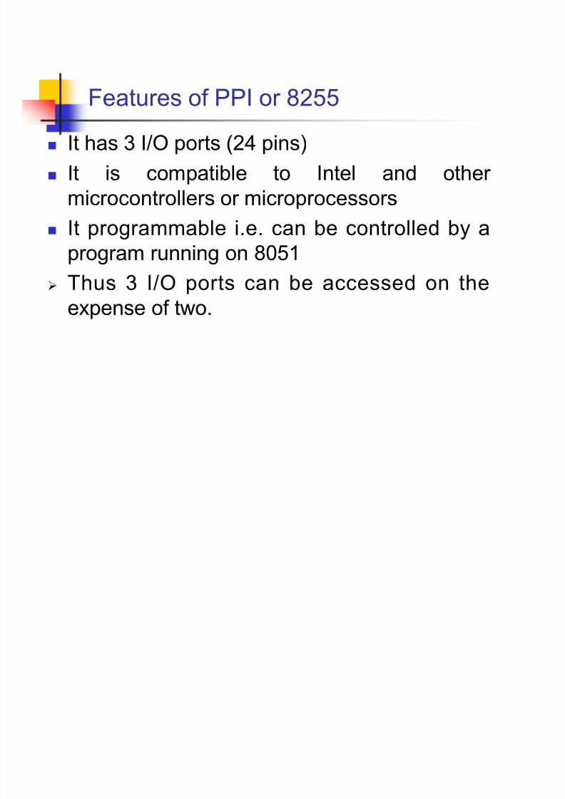
Features of PPI or 8255
It has 3 I/O ports (24 pins)
It is compatible to Intel and other
microcontrollers or microprocessors It programmable i.e. can be controlled by a
program running on 8051
Thus 3 I/O ports can be accessed on the
expense of two.

8/8/2019 24355464 8255 PPI Programmable Peripheral Interface
http://slidepdf.com/reader/full/24355464-8255-ppi-programmable-peripheral-interface 4/19
Pin Diagram
8/8/2019 24355464 8255 PPI Programmable Peripheral Interface
http://slidepdf.com/reader/full/24355464-8255-ppi-programmable-peripheral-interface 5/19
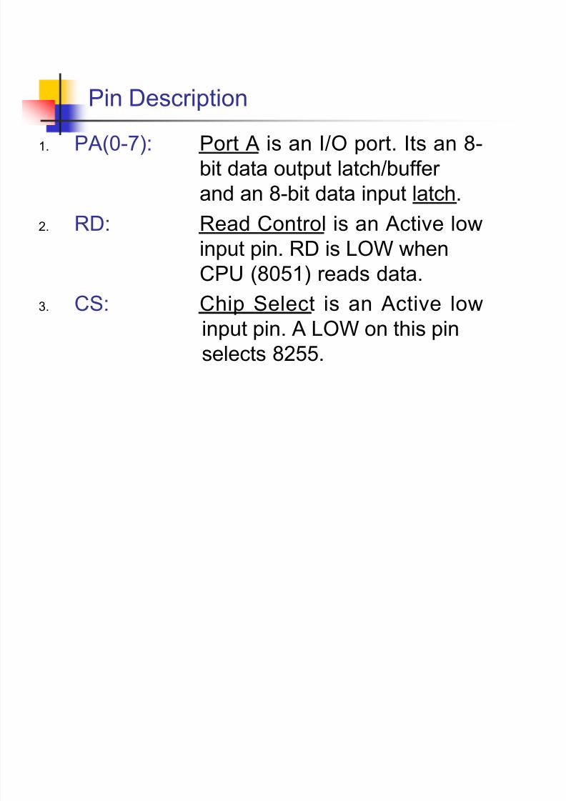
Pin Description
1. PA(0-7): Port A is an I/O port. Its an 8-
bit data output latch/buffer
and an 8-bit data input latch.2. RD: Read Control is an Active low
input pin. RD is LOW when
CPU (8051) reads data.
3. CS: Chip Select is an Active lowinput pin. A LOW on this pin
selects 8255.
8/8/2019 24355464 8255 PPI Programmable Peripheral Interface
http://slidepdf.com/reader/full/24355464-8255-ppi-programmable-peripheral-interface 6/19
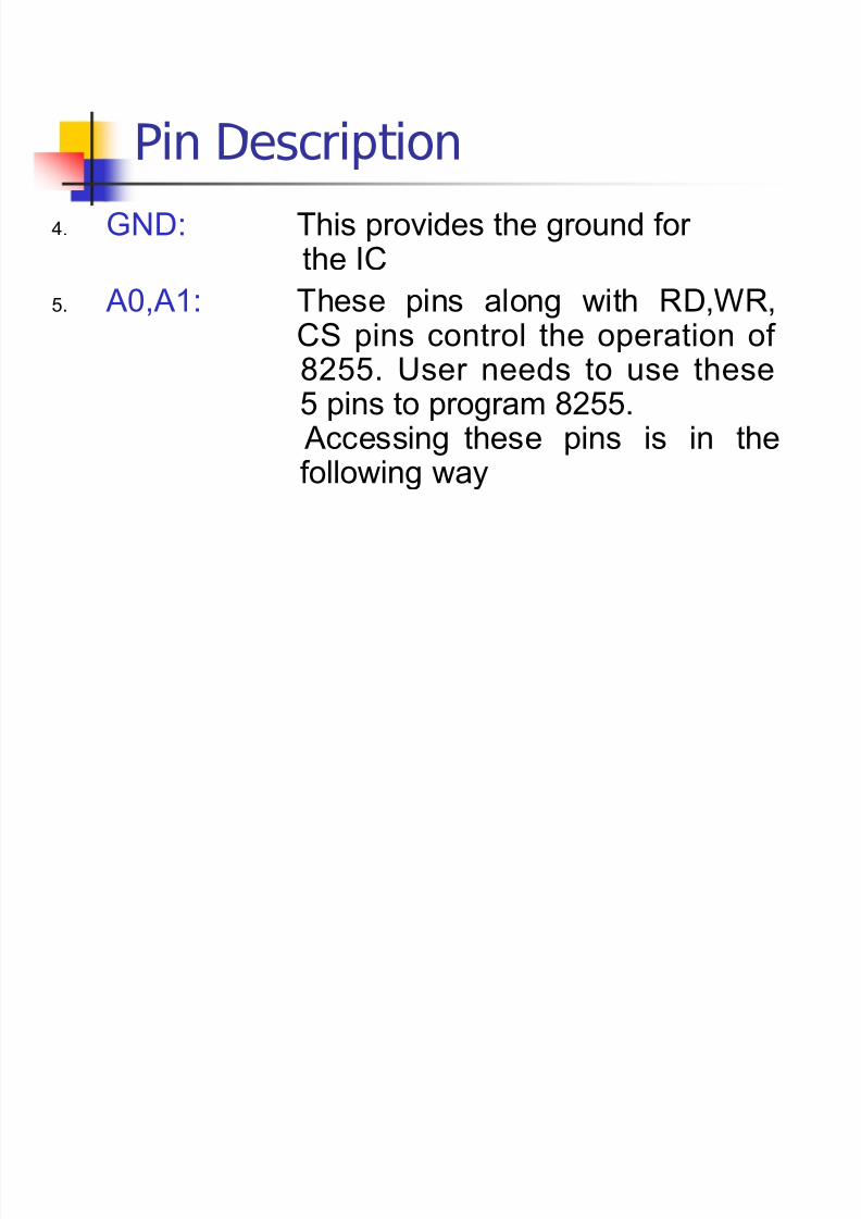
Pin Description4. GND: This provides the ground for
the IC
5. A0,A1: These pins along with RD,WR,CS pins control the operation of 8255. User needs to use these5 pins to program 8255.
Accessing these pins is in thefollowing way
8/8/2019 24355464 8255 PPI Programmable Peripheral Interface
http://slidepdf.com/reader/full/24355464-8255-ppi-programmable-peripheral-interface 7/19
Pin Description6. PC(0-7): Port C is an 8-bit I/O port. Its
lower 4-bits can be programmedto work in conjunction with PortBand the upper 4-bits can beprogrammed to work inconjunction with Port Aseparately.
7. PB(0-7): Port B is an 8-bit I/O port usedfor 8-bit output data latch/buffer or input data buffer.
8/8/2019 24355464 8255 PPI Programmable Peripheral Interface
http://slidepdf.com/reader/full/24355464-8255-ppi-programmable-peripheral-interface 8/19
Pin Description7. Vcc: +5V power supply.
8. D7-D0: Data bus, bidirectional, tristate
lines connected tosystem (8051) data lines
9. RESET: Reset is an input pin whichsets the PPI to its default state.
10. WR: Write Enable is an active lowinput pin.
11. NC: Pin numbers 1,12,23,24 on aPLCC package are left
unconnected.

8/8/2019 24355464 8255 PPI Programmable Peripheral Interface
http://slidepdf.com/reader/full/24355464-8255-ppi-programmable-peripheral-interface 9/19
Pin Description (Accessing 8255 using A0,
A1 ,RD ,WR ,CS pins)
8/8/2019 24355464 8255 PPI Programmable Peripheral Interface
http://slidepdf.com/reader/full/24355464-8255-ppi-programmable-peripheral-interface 10/19
Functional Description
Data Bus Buffer is a 3-state bidirectional 8-bit
buffer used to interface with system data bus.
Read/Write and Control Logic controls all of the internal and external transfer of both data
and control or status words.
Ports A, B, and C are each 8-bit ports which
can be configured by software. These also
offer a wide range of characteristics to the
system software.
8/8/2019 24355464 8255 PPI Programmable Peripheral Interface
http://slidepdf.com/reader/full/24355464-8255-ppi-programmable-peripheral-interface 11/19
Operational Description
8255 can be operated in three modes
Mode 0(Basic Input Output).
Mode 1(Strobed Input Output).
Mode 2(Bi-Directional Bus).
Any of the 8-bits of port C can be set or
reset. This feature supports control basedsoftware requirements.
8/8/2019 24355464 8255 PPI Programmable Peripheral Interface
http://slidepdf.com/reader/full/24355464-8255-ppi-programmable-peripheral-interface 12/19
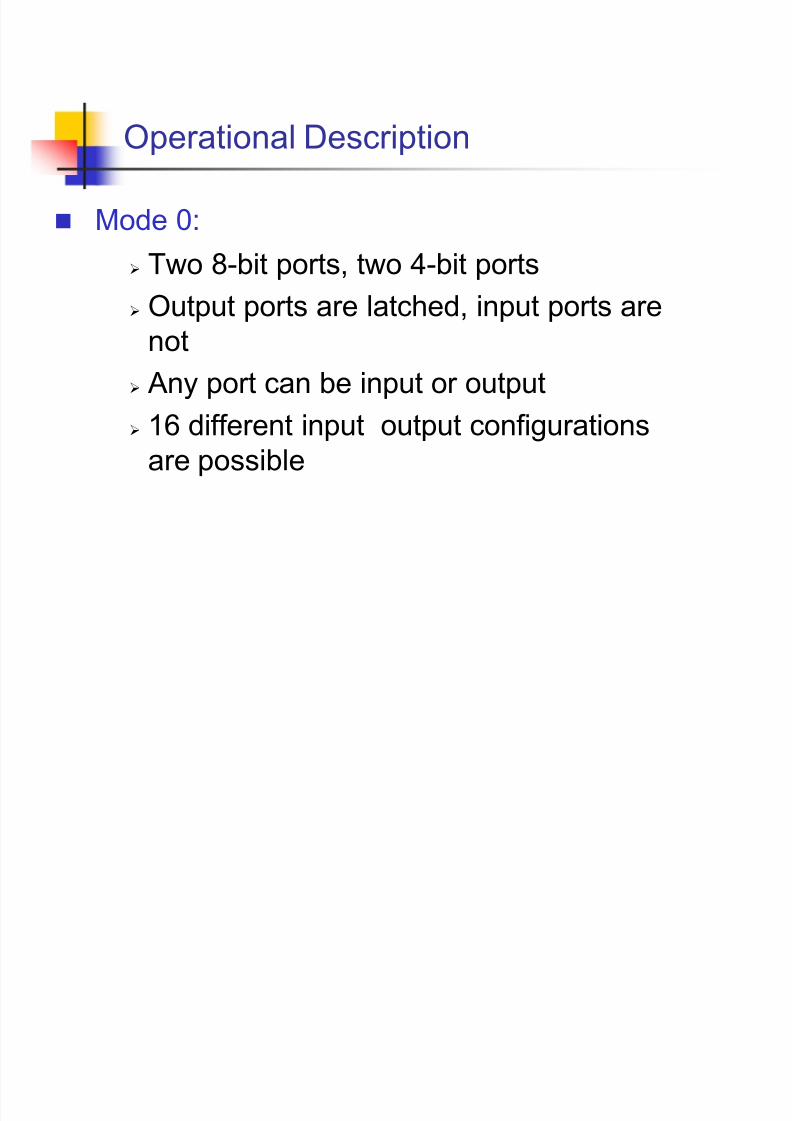
Operational Description
Mode 0:
Two 8-bit ports, two 4-bit ports Output ports are latched, input ports are
not
Any port can be input or output
16 different input output configurationsare possible

8/8/2019 24355464 8255 PPI Programmable Peripheral Interface
http://slidepdf.com/reader/full/24355464-8255-ppi-programmable-peripheral-interface 13/19
Operational Description Mode 1
Three ports are available as two groups.
Each port contains one 8- bit data port and one4- bit control port.
Both the data ports can either be input or output.
Both the input or output are latched.
The 4-bit port can be used as both control or
status port.

8/8/2019 24355464 8255 PPI Programmable Peripheral Interface
http://slidepdf.com/reader/full/24355464-8255-ppi-programmable-peripheral-interface 14/19
Operational Description Mode 2:
Used in group A only.
8-bit, bidirectional bus port (port A) and 5-bitcontrol port (port C).
Both inputs and outputs are latched.
The 5-bit control port (port C) is used for controlor status for the 8-bit, bidirectional bus (port A)
8/8/2019 24355464 8255 PPI Programmable Peripheral Interface
http://slidepdf.com/reader/full/24355464-8255-ppi-programmable-peripheral-interface 15/19
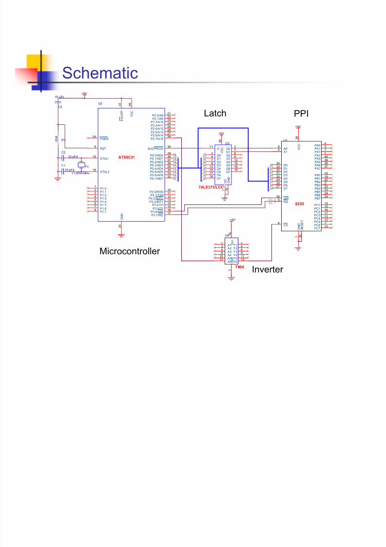
Schematic+5V
+5V
+5V
+5V
U6
7404
1 23 45 6
7
8 910 1112 13
1 4
A1 Y1 A2 Y2 A3 Y3
G n d
A4 Y4 A5 Y5 A6 Y6
V c c
U1
8255
3433323130292827
536
98
3 5
6
432140393837
1819202122232425
1415161713121110
2 6
7
D0D1D2D3D4D5D6D7
RD
WR
A0 A1
R E S E T
CS
PA0PA1PA2PA3PA4PA5PA6PA7
PB0PB1PB2PB3PB4PB5PB6PB7
PC0PC1PC2PC3PC4PC5PC6PC7
V C C
G N D
C3
10 uFd
C2
33 pFd
C1
33 pFd
R1 1 0 K
U2
AT89C51
9
18
19
2 0
29
30
3 1
4 0
12345
678
2122232425262728
10111213
14151617
3938373635343332
RST
XTAL2
XTAL1
G N D
PSEN
ALE/PROG
E A / V P P
V C C
P1.0P1.1P1.2P1.3
P1.4P1.5P1.6P1.7
P2.0/A8P2.1/A9
P2.2/A10P2.3/A11P2.4/A12P2.5/A13
P2.6/A14P2.7/A15
P3.0/RXDP3.1/TXD
P3.2/INTO
P3.3/INT1P3.4/TOP3.5/T1
P3.6/WRP3.7/RD
P0.0/AD0P0.1/AD1P0.2/AD2P0.3/AD3P0.4/AD4P0.5/AD5P0.6/AD6P0.7/AD7
Y1
11.0592 MHz
U3
74LS373/LCC
3478
13141718
1
11 256912151619
2 0
1 0
D0D1D2D3D4D5D6D7
O C
G Q0Q1Q2Q3Q4Q5Q6Q7
V C C
G N D
P3.6
P3.7
Inverter
Latch PPI
Microcontroller

8/8/2019 24355464 8255 PPI Programmable Peripheral Interface
http://slidepdf.com/reader/full/24355464-8255-ppi-programmable-peripheral-interface 16/19
Assembly Language Program for 8255 Data
Transfer
ORG 00h
MOV DPTR,#4003h ;Base address of the theControl Word Register of
8255 MOV A,#90h ;PA->input, PB->output,
PC->output
MOVX @DPTR,A ;Instructing Control register with Control Word
BACK:MOV DPTR,#4001h ;Base address of Port B
MOV A,#055h
MOVX @DPTR,A ;PB=0x55

8/8/2019 24355464 8255 PPI Programmable Peripheral Interface
http://slidepdf.com/reader/full/24355464-8255-ppi-programmable-peripheral-interface 17/19
MOV DPTR,#4002h ;Base Address of Port C
MOV A,#0AAh
MOVX @DPTR,A ;PC=0xaa ACALL DELAY ;Delay to check the o/p
MOV DPTR,#4001h
MOV A,#0AAh
MOVX @DPTR,A MOV DPTR,#4002h
8/8/2019 24355464 8255 PPI Programmable Peripheral Interface
http://slidepdf.com/reader/full/24355464-8255-ppi-programmable-peripheral-interface 18/19
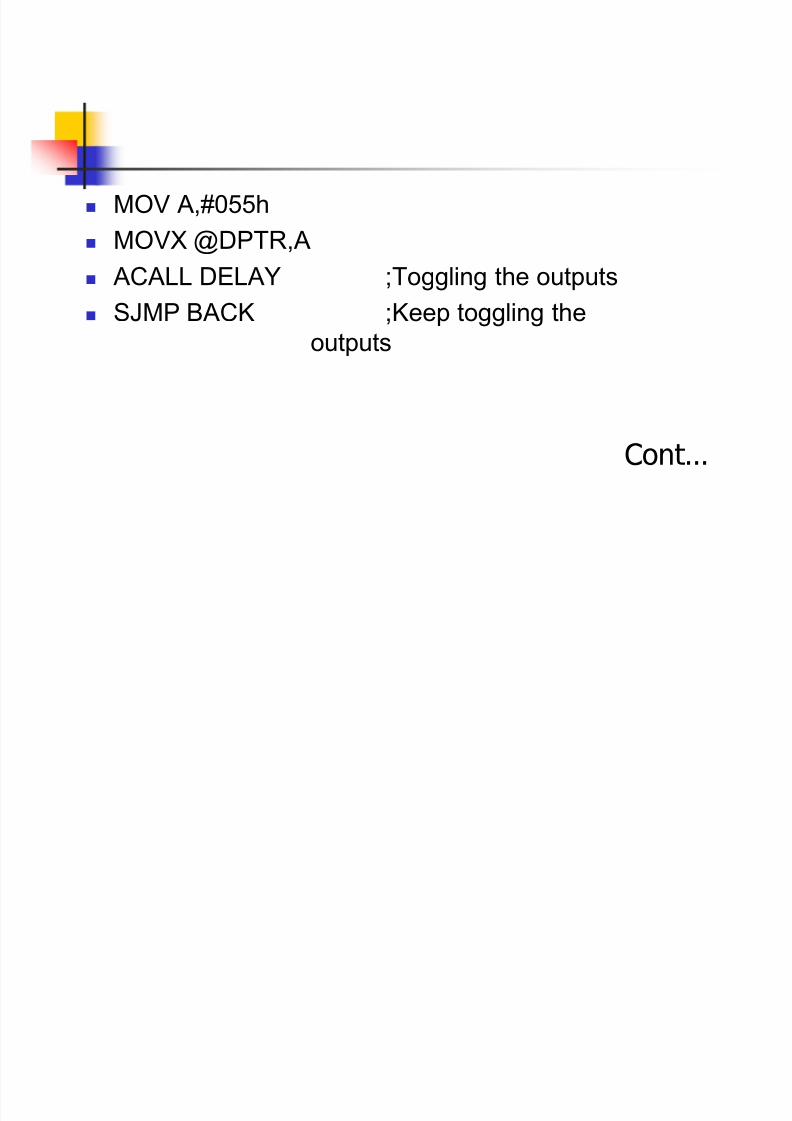
MOV A,#055h
MOVX @DPTR,A
ACALL DELAY ;Toggling the outputs SJMP BACK ;Keep toggling the
outputs
Cont

8/8/2019 24355464 8255 PPI Programmable Peripheral Interface
http://slidepdf.com/reader/full/24355464-8255-ppi-programmable-peripheral-interface 19/19
DELAY:
MOV R0,#0FFh
LOOP3:MOV R1,#0FFh
LOOP2:MOV R2,#0FFh ;to create a delay of 128*128*128*8 machinecycles
LOOP1: DJNZ R2,LOOP1
DJNZ R1,LOOP2
DJNZ R0,LOOP3 END ;may not reach
here....