24ghz lna and vector modulator phase shifter for … · 24ghz lna and vector modulator phase...
TRANSCRIPT

24 GHz LNA and Vector Modulator Phase Shifterfor Phased-Array Receiver in CMOS Technology
Ban Wang, Gabriele Tasselli, Cyril Botteron and Pierre-Andre Farine,Ecole Polytechnique Federale de Lausanne, Electronics and Signal Processing Laboratory, Neuchatel, Switzerland
Email: [email protected], [email protected], [email protected], [email protected]
Abstract—With the rapid development of the applications inshort range communication, phased-array receiver working at24 GHz can provide enhanced gain performance at desired trans-mission direction. Also there is the wide signal bandwidth, i.e.250 MHz free licensed spectrum at this frequency. In the phased-array front-end, the key component is the phase shifter, whichdecides the tuning resolution of beam-forming. The challenge ofthe design work comes from the low-power, low-noise and low-cost requirement. This paper explores the design procedure ofa Vector Modulation Phase Shifter (VMPS), consisting of a 90◦
hybrid, a variable gain amplifier and the Wilkinson combiner.The variable gain amplifier is fabricated in 90nm complementarymetal-oxide-semiconductor technology, and the passive hybridand the Wilkinson combiner are designed on the printed circuitboard with RO4003 substrate. After combining the measurementresults of each block, the VMPS shows 45◦ phase shifts with 7◦
phase error, and 9 mW consumption.
I. INTRODUCTION
The 24 GHz Industrial Scientific Medical (ISM) band isaccepted worldwide for Short Range Communication (SRC)and for the radio determination: detection, movement andalert applications [1], [2] and [3]. The Phased-Array (PhA)principle can be applied to add functionalities and improveperformances. For example, the beam steering functionalitycan be exploited by short range devices for interference mit-igation and to focus the antenna pointing towards the desiredtransmitter/receiver. In the radio determination application, thebeam steering technique can be used to scan the environmentto improve the spatial resolution of the sensor. The relativewide bandwidth, i.e. 250 MHz, allows the relatively highcapacities of the data throughput.
Moreover, SRC and sensors often require low power con-sumption and miniaturization. Therefore, the implementationof Phased-Array Front-End (PhA-FE) using the latest scaledCMOS technologies, ex. 90 nm, is the key point for a low-costand mass diffusion of these devices.
The challenge of developing such a PhA-FE is related onfollowing aspects: 1) The accuracy of the phase tuning decidesthe resolution of the system and the pointing direction of thetransmission wave. 2) The low-power performance determinesthe efficiency of the mobile device, which has to be acceptableunder the satisfaction of the noise and gain requirements.3) The parasitic effects are introduced from the circuit andlayout design. To avoid or release the potential parasitic effect,the usual way is to optimize the layout design with shortRF connections and matched architectures. In our work, wealso put ground grids on the first metal layer and also some
sensitive parts of other metal layers to decrease the parasiticinductance to the silicon substrate.
In this paper, we report the implementation of two blocks:Low Noise Amplifier (LNA) and Vector Modulation PhaseShifter (VMPS) that are the basic elements of a local oscillatorPhA architecture. The single stage LNA is fabricated in90nm Complementary Metal-Oxide-Semiconductor (CMOS)technology, and it shows 6.5 dB gain, 3.2 dB simulated noisefigure, with consumption of 4.3 mW. The VMPS consists of a90◦ hybrid, a Variable Gain Amplifier (VGA) and the Wilkin-son combiner. The VGA is derived from the LNA design, andalso fabricated in 90nm CMOS technology. Passive blocks,i.e. hybrid and combiner are manufactured separately on thePrinted Circuit Board (PCB) with hydrocarbon fiber glass(RO4003) substrate. With S-parameter measurement results,the VMPS has been set up in the simulation tool. It shows45◦ phase shift resolution with 7◦ phase error, and 9 mWconsumption.
II. CIRCUIT BLOCKS
The local oscillator PhA architecture, shown in Fig. 1, hasbeen selected for its efficiency and versatility as stated in ourprevious work, [4] and [5].
Fig. 1: Local oscillator phased-array architecture
In the receiver architecture, at each signal branch, theLNA is placed following at the receiving antennas. At LocalOscillator (LO) path, the VMPS controls the phase of thecarrier frequency signal, in order to compensate phase delayfrom the receiving signal. After mixing with the RF paths,signals from each branch combine together and flow to theback-end.

The following sections will present the block developmentof the single stage LNA, the VGA and the VMPS. LNA con-stitutes the base element of a VGA, which is in turn the basicblock of the VMPS. As mentioned in the introduction, VMPSconsists two VGAs, a 90◦ hybrid and a Wilkinson combiner.The last two components are designed and fabricated on PCB.Finally, the performance of the VMPS has been simulated byusing the measured S-parameters of all blocks.
A. Low Noise Amplifier
The LNA uses typical cascode structure to carry out themaximum gain from the single stage amplifier, seen in Fig.2(a). The degenerative inductance on the source is abandonedto preserve gain, and also because a little degeneration ispresent due to the parasitic inductance in the chip layout. Fromthe measurement, it shows 6.5 dB gain drawing only 3.6 mAat 1.2 V. The input return loss is -15 dB, as shown in Fig.3. The simulated noise figure is 3.2 dB. Table. I shows theperformance comparison with the state of the art. All of theworks listed are common-source single-end LNA.
M0
M1
L2
L1
Cos
CopRFin
RFout
CpCs
Rb
M2
R
G
GR
G
GVdd
W: 24umL: 90nm
W: 24umL: 90nm
Vb
W: 2umL: 90nm
(a) Schematic of 1st-stage LNA (b) Die photo of 1st-stage LNA
Fig. 2: Schematic and the Die photo of the LNA
TABLE I: Comparison of the 24 GHz LNA performances.
Reference [6] [7] [8] This workFrequency (GHz) 24.0 24.0 24.0 24.0Technology (nm) 90 130 90 90
Gain (dB) 7.5 19a 15.2a 6.5Input matching (dB) -16 -16 -12 -15Noise Figure (dB) 3.2 3.8 2.9 3.2b
Power Cons. (mW) 10.6 15 9.1 4.3
a Two-stage b Simulated
B. Variable Gain Amplifier
The design of the VGA has derived from the LNA scheme.Fig. 4(a) shows the modification on the two groups of upperMOSFETs of the cascode: M1 and M3 connected to theresonant load; M2 and M4 connected to the power supply. Theamplifier gain is controlled by steering the current between twogroups of MOSFETs. In each group, there are two MOSFETs,which can implement 2-bit tuning (three meaningful states),limited by our probe station capabilities. The maximum gainstate is obtained when G0 and G1 are low, so that M2and M4 are biased for the same current as M0, while M1
(a) Simulated and measured LNA gain
(b) Simulated and measured LNA return loss
Fig. 3: Simulated and measured results of 1-stage LNA.
and M3 are switched off. Half gain state is obtained whenG1 is high and G0 is low. When G0 and G1 both arehigh, the circuit shows the isolation state. In this way thecontrol scheme is scalable over the number of bits. Withoutconsidering the measurement limitations, the VGA can bedesigned for 5-bit phase tuning by splitting the total width ofone group (ex. M2+M4) of transistors to 5 pairs, i.e. 30, 15,7.5, 3.25 and 3.25 um. With this current steering techniques,the input impedance is kept constant over the amplifier gain,contributing to the phase accuracy of the phase shifter. Thephoto of the VGA chip is shown in Fig. 4(b) and the size ofthe chip is 0.3 mm×0.15 mm, and 0.6 mm×0.6 mm includingthe pads. The measured VGA can obtain 5.9 dB of maximumgain and 3.1 dB half gain, illustrated in Fig. 5(a). Thanks to thebalanced current steering scheme, at different states, phases arestable, ex. at 24.1 GHz, the phase difference is 5◦. The powerconsumption is 4.5 mW, with the supply voltage 1.2 V. Table.II shows the comparison of our work with the state of the art.
C. Vector Modulator Phase Shifter
The architecture of the VMPS is shown in Fig. 6. Thefirst stage is the 90◦ hybrid, which generates the quadrantinput signals. Hence, the amplitude of the I and Q paths arecontrolled by the VGA described in Section II-B. And the

M0
M4
Lo
L
Cos
Cop
RFout
CpCs Rb
Vb
G
G
M3
Vdd
OUT
Vdd
RFinG
G
W: 45umL: 90nm
W: 15umL: 90nm
M2M1
0G 1G1G0G
W: 45umL: 90nm
W: 15umL: 90nm
(a) Schematic of VGA (b) Die photo of VGA
Fig. 4: Schematic and the die photo of the VGA.
(a) VGA measured gain for programmed states
(b) VGA measured phase for programmed states
Fig. 5: VGA measurement results.
TABLE II: Comparison of the measured results of the VGA
Reference [9] [10] [11] This workTechnology (nm) 90 180 130 90Frequency (GHz) 4.93 21 26 23.8Max. Gain (dB) 12.2 3 5 5.9
Tuning states (bit) 6 3 4 2Power Cons. (mW) 28 112 4.5 4.5
weighted components are added by means of a Wilkinsoncombiner.
90° Hybrid
0°
90°
Wilkinson
VGAI path
Q path
Fig. 6: VMPS scheme used in the simulation
TABLE III: Performance comparison of VMPS
Reference [12]a [13] [14] This workFrequency (GHz) 24 24 60 24.125Technology (nm) 130 130 90 90c
Tuning res. (◦) 25 22.5 11.25 45Gain (dB) -2 -3 9 -4.2d
Phase Imbalance (◦) N/A 11b 3 7Gain Imbalance (dB) 3 1.8b N/A 0.36
Total Power Cons. (mW) 21.36 11.7 60 9
a Simulation results. b RMS error.c Not integrate in one chip. d Average gain among three states.
The 90◦ hybrid, shown in Fig. 7(a), is derived from theWilkinson combiner adding a 90◦ length transmission linein one path. The measured S-parameters of this structure areshown in Fig. 7(b). The phase difference between its outputshas been designed as 90◦ with less than 2◦ of imbalance. Theinsertion loss has less than 0.5 dB imbalance. The Wilkinsoncombiner, after the VGAs, shows 5 dB insertion loss and aperfect phase matching of two branches. Both passive blocksare fabricated on the low-loss Rogers RO4003 substrate.
The state with maximum gain on I path and isolation on Qpath is taken as the reference, therefore, when the VGA at Ipath is set to isolation state, while the VGA at Q path reachesfull gain, the combined signal should show 90◦ phase shift,and if both VGAs are at half gain states, the output signalshould get 45◦ phase shift.
The simulation of the overall VMPS has been implementedin Advanced Design System software environment, based onthe measured S-parameters of each block in Fig. 6. In Fig.8(a) and 8(b), the resulting gain imbalance is within 1 dB at24.13 GHz over the other two programmed states (45◦ and 90◦
phase shift). For the phase difference, it can be distinguishedthat 45◦ phase shift has been set between each state, with 6.9◦
and 3.2◦ phase error respectively. The comparison of our workwith the state of the art is presented in Table. III.
III. CONCLUSION
The developed blocks are suitable for a low-power imple-mentation of the PhA-FE as shown in the comparison with thestate-of-the-art. The evident power saving does not sacrificemuch other performances. Indeed, for the LNA, a good noisefigure and input return loss are achieved and the gain iswithin 1 dB with the other single stage LNA reported in TableI. Also the VGA shows the minimum power consumptionwhile keeping good gain, as shown in Table II. Finally, in
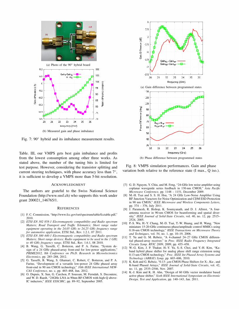
(a) Photo of the 90◦ hybrid board
(b) Measured gain and phase imbalance
Fig. 7: 90◦ hybrid and its imbalance measurement results.
Table. III, our VMPS gets best gain imbalance and profitsfrom the lowest consumption among other three works. Asstated above, the number of the tuning bits is limited fortest purpose. However, considering the transistor splitting andcurrent steering techniques, with phase accuracy less than 7◦,it is sufficient to develop a VMPS more than 5-bit resolution.
ACKNOWLEDGMENT
The authors are grateful to the Swiss National ScienceFoundation (http://www.snsf.ch) who supports this work undergrant 200021 146765/1.
REFERENCES
[1] F. C. Commission, “http://www.fcc.gov/oet/spectrum/table/fcctable.pdf,”2010.
[2] ETSI EN 302 858-1 Electromagnetic compatibility and Radio spectrumMatters; Road Transport and Traffic Telematics; Short range radarequipment operating in the 24,05 GHz to 24,25 GHz frequency rangefor automotive application, ETSI Std., Rev. 1.2.1, 07 2011.
[3] ETSI EN 300 440-1 Electromagnetic compatibility and Radio spectrumMatters; Short range devices; Radio equipment to be used in the 1 GHzto 40 GHz frequency range, ETSI Std., Rev. 1.6.1, 08 2010.
[4] B. Wang, G. Tasselli, C. Botteron, and P. A. Farine, “System de-sign of a 24 GHz phased-array front-end for low-power applications,”PRIME2012, 8th Conference on Ph.D. Research in MicroelectronicsElectronics, pp. 285–288, 2012.
[5] G. Tasselli, B. Wang, S. Ghamari, C. Robert, C. Botteron, and P. A.Farine, “Development of a versatile low-power 24 GHz phased arrayfront-end in 90 nm CMOS technology,” 10th IEEE International NEW-CAS Conference, no. c, pp. 465–468, Jun. 2012.
[6] O. Dupuis, X. Sun, G. Carchon, P. Soussan, M. Ferndah, S. Decoutere,and W. D. Raedt, “24GHz LNA in 90nm RF-CMOS with high-Q above-IC inductors,” IEEE ESSCIRC, pp. 89–92, September 2005.
(a) Gain difference between programmed states
(b) Phase difference between programmed states
Fig. 8: VMPS simulation performances. Gain and phasevariation both relative to the reference state (I max., Q iso.).
[7] G. D. Nguyen, Y. Chiu, and M. Feng, “24-GHz low noise amplifier usingcoplanar waveguide series feedback in 130-nm CMOS,” Asia PacificMicrowave Conference, pp. 1148 – 1151, December 2009.
[8] M.-H. Tsai and S. S. H. Hsu, “A 24 GHz Low-Noise Amplifier UsingRF Junction Varactors for Noise Optimization and CDM ESD Protectionin 90 nm CMOS,” IEEE Microwave and Wireless Components Letters,pp. 374 – 376, July 2011.
[9] J. Paramesh, R. Bishop, K. Soumyanath, and D. J. Allstot, “A four-antenna receiver in 90-nm CMOS for beamforming and spatial diver-sity,” IEEE Journal of Solid-State Circuits, vol. 40, no. 12, pp. 2515–2524, 2005.
[10] P.-S. Wu, H.-Y. Chang, M.-D. Tsai, T.-W. Huang, and H. Wang, “Newminiature 15-20-GHz continuous-phase/amplitude control MMICs using0.18-um CMOS technology,” IEEE Transactions on Microwave Theoryand Techniques, vol. 54, no. 1, pp. 10–19, 2006.
[11] T. Yu and G. M. Rebeiz, “A 4-channel 24–27 GHz CMOS differen-tial phased-array receiver,” in Proc. IEEE Radio Frequency IntegratedCircuits Symp. RFIC 2009, 2009, pp. 455–458.
[12] W.-G. Kim, J. P. Thakur, H.-Y. Yu, S.-S. Choi, and Y.-H. Kim, “Ka-band hybrid phase shifter for analog phase shift range extension using0.13-um CMOS technology,” Proc. IEEE Int Phased Array Systems andTechnology (ARRAY) Symp, pp. 603–606, 2010.
[13] K. Koh and G. Rebeiz, “0.13- µm CMOS Phase Shifters for X-, Ku-, andK-band Phased Arrays,” IEEE Journal of Solid-State Circuits, vol. 42,no. 11, pp. 2535–2546, Nov. 2007.
[14] K.-J. Kim and K. H. Ahn, “Design of 60 GHz vector modulator basedactive phase shifter,” Sixth IEEE International Symposium on ElectronicDesign, Test and Application, pp. 140–143, Jan. 2011.