250ks/s, 16-bit, 64-ch analog input card with universal...
TRANSCRIPT
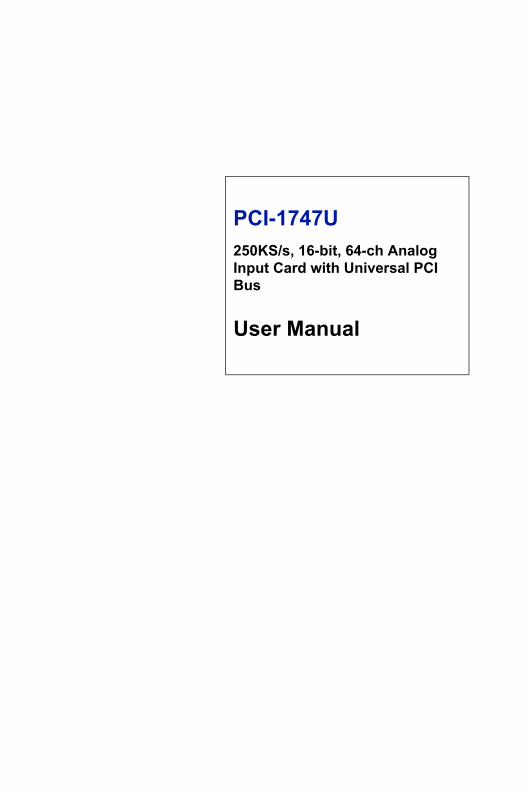
PCI-1747U250KS/s, 16-bit, 64-ch Analog Input Card with Universal PCI Bus
User Manual

CopyrightThe documentation and the software included with this product are copy-righted 2004 by Advantech Co., Ltd. All rights are reserved. Advantech Co., Ltd. reserves the right to make improvements in the products described in this manual at any time without notice. No part of this man-ual may be reproduced, copied, translated or transmitted in any form or by any means without the prior written permission of Advantech Co., Ltd. Information provided in this manual is intended to be accurate and reli-able. However, Advantech Co., Ltd. assumes no responsibility for its use, nor for any infringements of the rights of third parties, which may result from its use.
AcknowledgementsMicrosoft Windows and MS-DOS are registered trademarks ofMicrosoft Corp.All other product names or trademarks are properties of their respective owners.
Part No. 2003174701 2nd EditionPrinted in Taiwan October 2005
PCI-1747U User Manual ii
Product Warranty (2 years)Advantech warrants to you, the original purchaser, that each of its prod-ucts will be free from defects in materials and workmanship for two years from the date of purchase. This warranty does not apply to any products which have been repaired or altered by persons other than repair personnel authorized by Advantech, or which have been subject to misuse, abuse, accident or improper instal-lation. Advantech assumes no liability under the terms of this warranty as a consequence of such events.Because of Advantechs high quality-control standards and rigorous test-ing, most of our customers never need to use our repair service. If an Advantech product is defective, it will be repaired or replaced at no charge during the warranty period. For out-of-warranty repairs, you will be billed according to the cost of replacement materials, service time and freight. Please consult your dealer for more details.
If you think you have a defective product, follow these steps:1. Collect all the information about the problem encountered. (For
example, CPU speed, Advantech products used, other hardware and software used, etc.) Note anything abnormal and list any onscreen messages you get when the problem occurs.
2. Call your dealer and describe the problem. Please have your man-ual, product, and any helpful information readily available.
3. If your product is diagnosed as defective, obtain an RMA (return merchandize authorization) number from your dealer. This allows us to process your return more quickly.
4. Carefully pack the defective product, a fully-completed Repair and Replacement Order Card and a photocopy proof of purchase date (such as your sales receipt) in a shippable container. A product returned without proof of the purchase date is not eligible for war-ranty service.
5. Write the RMA number visibly on the outside of the package and ship it prepaid to your dealer.
iii
CEThis product has passed the CE test for environmental specifications. Test condi-tions for passing included the equipment being operated within an industrial enclosure. In order to protect the product from being damaged by ESD (Electro-static Discharge) and EMI leakage, we strongly recommend the use of CE-com-pliant industrial enclosure products.
FCC Class AThis equipment has been tested and found to comply with the limits for a Class A digital device, pursuant to Part 15 of the FCC Rules. These limits are designed to provide reasonable protection against harmful interference when the equipment is operated in a commercial environment. This equipment generates, uses and can radiate radio frequency energy and, if not installed and used in accordance with the instruction manual, may cause harmful interference to radio communications. Operation of this equipment in a residential area is likely to cause harmful inter-ference in which case the user will be required to correct the interference at own expense.
Technical Support and AssistanceStep 1. Visit the Advantech web site at www.advantech.com/support
where you can find the latest information about the product.Step 2. Contact your distributor, sales representative, or Advantech's cus-
tomer service center for technical support if you need additional assistance. Please have the following information ready:- Product name and serial number- Description of your peripheral attachments- Description of your software (OS, version, software, etc.)- A complete description of the problem- The exact wording of any error messages
Packing ListBefore setting up the system, check that the items listed below are included and in good condition. If any item does not accord with the table, please contact your dealer immediately. 1 x PCI-1747U card 1 x Companion CD-ROM (DLL driver included) 1 x User Manual (This manual)
PCI-1747U User Manual iv
ContentsChapter 1 Introduction ..................................................... 2
1.1 Introduction ....................................................................... 21.2 Features ............................................................................. 2
1.2.1 Auto-Calibration Function ............................................. 21.2.2 BoardID ......................................................................... 31.2.3 Plug-and-Play Function ................................................. 31.2.4 Automatic Channel/Gain/SD/BU Scanning ................... 31.2.5 PCIBus Mastering Data Transfer ................................. 31.2.6 On-board FIFO Memory ................................................ 31.2.7 On Board Programmable Timer/Counter ...................... 4
1.3 Installation Guide .............................................................. 4Figure 1.1:Installation Flow Chart ................................. 5
1.4 Software ............................................................................ 61.5 Accessories........................................................................ 6
1.5.1 PCL-10168 Wiring Cable .............................................. 61.5.2 ADAM-3968 Wiring Boards ......................................... 6
Chapter 2 Installation ....................................................... 82.1 Unpacking ......................................................................... 82.2 Driver Installation ............................................................. 9
Figure 2.1:Setup Screen ................................................. 9Figure 2.2:Driver Setup ............................................... 10
2.3 Hardware Installation ...................................................... 11Figure 2.3:Device Manager ......................................... 12
2.4 Device Setup & Configuration........................................ 13Figure 2.4:Device Manager dialog box ....................... 14Figure 2.5:Figure 2.5 The Device Setting dialog box .. 15
2.5 Auto-Calibration.............................................................. 152.5.1 Test Point ..................................................................... 16
Figure 2.6:Locations of test points .............................. 16Figure 2.7:Auto-Calibration dialog box ....................... 17Figure 2.8:A/D Auto-Calibration is finished. .............. 17
2.6 Device Testing................................................................. 18Figure 2.9:Device Test dialog box ............................... 18
Chapter 3 Signal Connections ........................................ 203.1 I/O Connector.................................................................. 20
3.1.1 I/O Connector Signal Description ................................ 20Table 3.1:I/O Connector Signal Description ............... 20
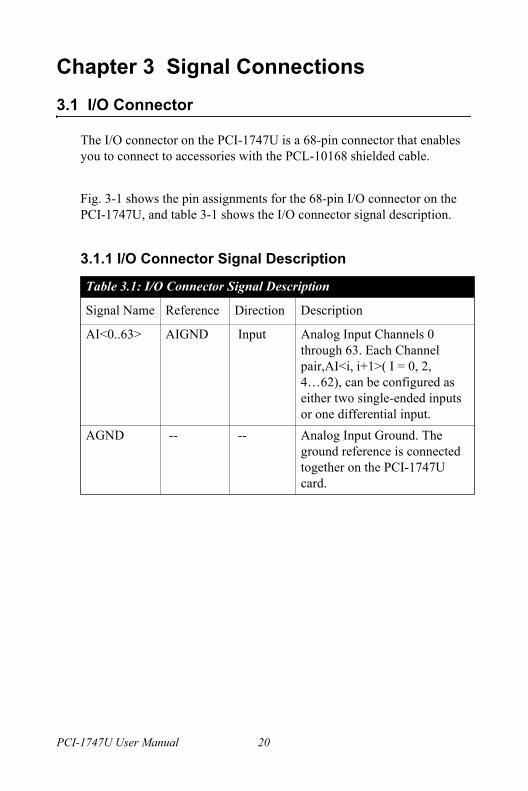
3.1.2 Pin Assignment ............................................................ 21Figure 3.1:I/O Connector Pin Assignments ................. 21
3.2 Analog Input Connections .............................................. 223.2.1 Single-ended Channel Connections ............................. 22
Figure 3.2:Single-ended Channel Connections .......... 22
v
3.2.2 Differential Channel Connections ............................... 23Figure 3.3:Differential Connection - Ground Signal ... 23Figure 3.4:Differential Connection - Floating Signal .. 24Figure 3.5:Example ...................................................... 25
3.3 Trigger Source Connections............................................ 253.3.1 Internal Pacer Trigger Connection ............................... 25
3.4 Switch and Jumper Settings ............................................ 26Figure 3.6:Jumpers and Switch Locations ................... 26
3.4.1 JP1 ................................................................................ 263.4.2 Board ID ...................................................................... 27
Chapter 4 Software Overview ........................................ 304.1 Software Overview.......................................................... 304.2 Programming Choices .................................................... 30
4.2.1 DLL Driver .................................................................. 304.2.2 Register-Level Programming ....................................... 30
4.3 DLL Driver Programming Roadmap ............................. 314.3.1 Programming Tools ..................................................... 314.3.2 Programming with DLL Driver Function Library ....... 324.3.3 Troubleshooting DLL Driver Error ............................. 33
Appendix A Specifications ................................................. 36A.1 Analog Input.................................................................... 36A.2 General ............................................................................ 37
Appendix B Block Diagram............................................... 40Appendix C Register Structure and Format.................... 42
C.1 Overview ........................................................................ 42C.2 I/O Port Address Map .................................................... 42
Table C.1:PCI-1747U Register Format (Part 1) .......... 43C.3 A/D Data BASE+0 and BASE+1............................... 47
Table C.2:PCI-1747U Register for A/D data ............... 47C.4 Software A/D Trigger BASE+0 ................................ 47C.5 A/D Channel Range Setting BASE+2 ....................... 48
Table C.3:Register for A/D channel range setting ....... 48Table C.4:Gain codes for PCI-1747U .......................... 49
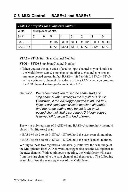
C.6 MUX Control BASE+4 and BASE+5........................ 50Table C.5:Register for multiplexer control .................. 50
C.6.1 Example 1 .................................................................... 51C.6.2 Example 2 .................................................................... 51
C.7 Control Register BASE+6 and BASE+7.................... 52Table C.6:Control Register .......................................... 52
C.8 Status Register BASE+6 and BASE+7 ...................... 54Table C.7:Status Register ............................................ 54
C.9 Clear Interrupt and FIFO BASE+8 and BASE+9 ..... 55Table C.8:Register to Clear Interrupt and FIFO .......... 55
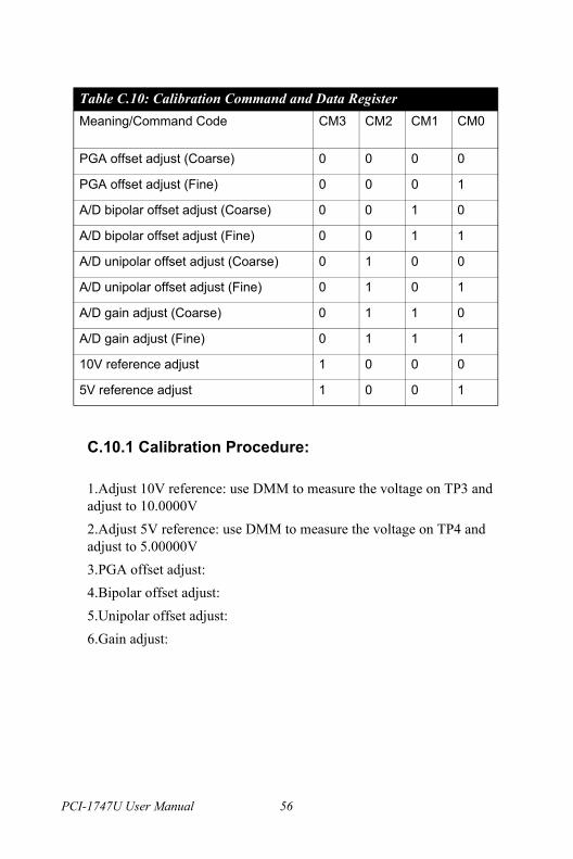
C.10 Calibration Registers BASE+18 and BASE+19 ........ 55Table C.9:Calibration Command and Data Register ... 55Table C.10:Calibration Command and Data Register . 56
C.10.1 Calibration Procedure: ................................................. 56
PCI-1747U User Manual vi
C.11 Board ID Registers BASE+20 .................................. 57Table C.11:Register for Board ID ................................ 57
C.12 Programmable Timer/Counter Registers......................... 57Appendix D 82C54 Counter Chip Function..................... 60
D.1 The Intel 82C54............................................................... 60D.2 Counter Read/Write and Control Registers..................... 61
Table D.1: ................................................................... 61D.2.1 Description ................................................................... 61
D.3 Counter Operating Modes .............................................. 64
vii

PCI-1747U User Manual viii
2
CH
AP
TE
R 1Introduction
This chapter introduces PCI-1747U and shows how to install the software. It also has information on useful accesso-ries.Sections include:
Introduction Features Installation Guide Software Accessories
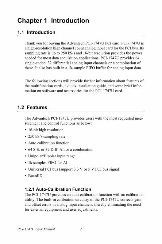
Chapter 1 Introduction1.1 Introduction
Thank you for buying the Advantech PCI-1747U PCI card. PCI-1747U is a high-resolution high channel count analog input card for the PCI bus. Its sampling rate is up to 250 kS/s and 16-bit resolution provides the power needed for most data acquisition applications. PCI-1747U provides 64 single-ended, 32 differential analog input channels or a combination of these. It also has built in a 1k-sample FIFO buffer for analog input data.
The following sections will provide further information about features of the multifunction cards, a quick installation guide, and some brief infor-mation on software and accessories for the PCI-1747U card.
1.2 Features
The Advantech PCI-1747U provides users with the most requested mea-surement and control functions as below: 16-bit high resolution 250 kS/s sampling rate Auto calibration function 64 S.E. or 32 Diff. AI, or a combination Unipolar/Bipolar input range 1k samples FIFO for AI Universal PCI bus (support 3.3 V or 5 V PCI bus signal) BoardID
1.2.1 Auto-Calibration FunctionThe PCI-1747U provides an auto-calibration function with an calibration utility. The built-in calibration circuitry of the PCI-1747U corrects gain and offset errors in analog input channels, thereby eliminating the need for external equipment and user adjustments.
PCI-1747U User Manual 2
1.2.2 BoardIDThe PCI-1747U has a built-in DIP switch that helps define each cards unique ID when multiple PCI-1747U cards have been installed on the same PC chassis. The BoardID setting function is very useful when build-ing a system with multiple PCI-1747U cards. With the correct BoardID settings, you can easily identify and access each card during hardware configuration and software programming.
1.2.3 Plug-and-Play FunctionThe PCI-1747U is a Plug-and-Play device, which fully complies with PCI Specification Rev 2.2. During card installation, there is no need to set jumpers or DIP switches. Instead, all bus-related configurations such as base I/O address and interrupt are automatically done by the Plug-and-Play function.
1.2.4 Automatic Channel/Gain/SD/BU ScanningThe PCI-1747U features an automatic channel/gain/SD/BU scanning cir-cuit. This circuit controls multiplexer switching during sampling in a way that is more efficient than software implementation. An on-board SRAM stores different gain, SD (Single-Ended/Differential) and BU (Bipolar/Unipolar) values for each channel. This combination lets users perform multi-channel high-speed sampling with different gain, SD and BU val-ues for each channel.
1.2.5 PCIBus Mastering Data TransferPCI-1747U supports PCI-Bus mastering DMA for high-speed data trans-fer and gap-free analog input. By setting aside a block of memory in the PC, the PCI-1747U performs bus-mastering data transfers without CPU intervention, setting the CPU free to perform more urgent tasks such as data analysis and graphics manipulation. The function makes it possible to run all I/O functions simultaneously at full speed without losing data.
1.2.6 On-board FIFO MemoryPCI-1747U provides 1K samples on-board FIFO (First In First Out) memory buffer for AD. This is an important feature for faster data trans-fer and more predictable performance under the Windows system.
3 Chapter 1

1.2.7 On Board Programmable Timer/CounterPCI-1747U provides a programmable timer counter for generating a pacer trigger for the A/D conversion. The timer/counter chip is 82C54, which includes three 16-bit counter 10 MHz clocks. Two counters are cascaded together to make a 32-bit timer for pacer trigger time base.
1.3 Installation Guide
Before you install your PCI-1747U card, please make sure you have the following necessary components: PCI-1747U analog input card PCI-1747U User Manual Driver software Advantech DLL drivers (included in the companion
CD-ROM) Wiring cable PCL-10168 Wiring board ADAM-3968 Computer Personal computer or workstation with a PCI-bus slot(
running Windows 98/2000/XP)Some other optional components are also available for enhanced opera-tion: Application software ActiveDAQ, GeniDAQ or other third-party soft-
ware packages
After you get the necessary components and maybe some of the accesso-ries for enhanced operation of your Multifunction card, you can then begin the Installation procedures. Fig. 1-1 on the next page provides a concise flow chart to give users a broad picture of the software and hard-ware installation procedures:
PCI-1747U User Manual 4
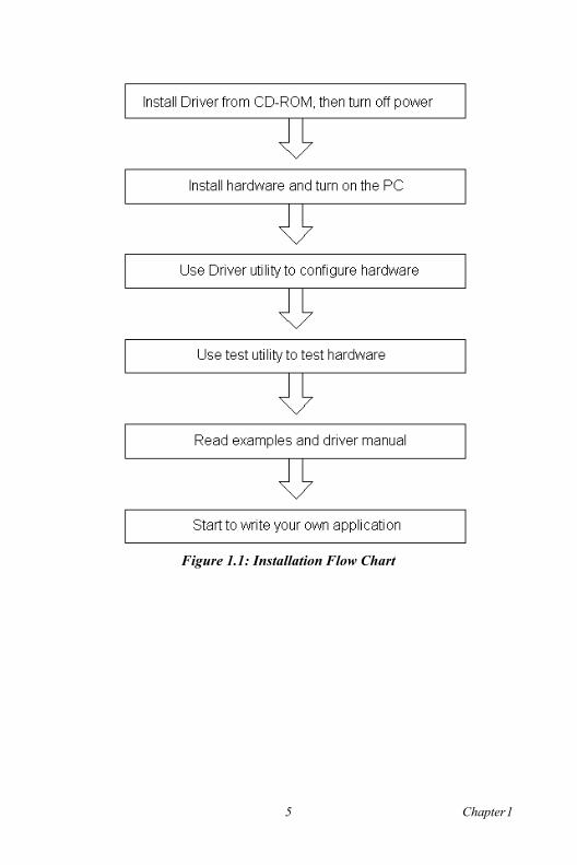
Figure 1.1: Installation Flow Chart
5 Chapter 1
1.4 Software
Advantech offers a rich set of DLL drivers, third-party driver support and application software to help fully exploit the functions of your PCI-1747U card: DLL driver (on the companion CD-ROM) LabVIEW driver Advantech ActiveDAQ Advantech GeniDAQ
For more information on software, please refer to Chapter 4, Software Overview.Users who intend to program directly at the registers of the Multifunction card have register-level programming as an option. Since register-level programming is often difficult and labor-intensive, it is usually recom-mended only for experienced programmers. For more information, please refer to Appendix C, Register Structure and Format.
1.5 Accessories
Advantech offers a complete set of accessory products to support the PCI-1747U cards. These accessories include:
1.5.1 PCL-10168 Wiring CableThe PCL-10168 shielded cable is specially designed for PCI-1747U cards to provide high resistance to noise. To achieve a better signal quality, the signal wires are twisted in such a way as to form a twisted-pair cable, reducing cross-talk and noise from other signal sources. Furthermore, its analog and digital lines are separately sheathed and shielded to neutralize EMI/EMC problems.
1.5.2 ADAM-3968 Wiring BoardsThe ADAM-3968 is a 68-pin SCSI wiring terminal module for DIN-rail mounting. This terminal module can be readily connected to the Advan-tech PC-Lab cards and allow easy yet reliable access to individual pin connections for the PCI-1747U card.
PCI-1747U User Manual 6

2
CH
AP
TE
R 2Installation
This chapter provides a packaged item checklist, proper instructions about unpacking and step-by-step procedures for both driver and card installation.Note that PCI-1747U is used as an example.Sections include:
Unpacking Driver Installation Hardware Installation Device Setup & Configuration Device Testing

Chapter 2 Installation2.1 Unpacking
After receiving your PCI-1747U package, please inspect its contents first. The package should contain the following items: PCI-1747U card Companion CD-ROM (DLL driver included) User ManualThe PCI-1747U card harbors certain electronic components vulnerable to electrostatic discharge (ESD). ESD could easily damage the integrated circuits and certain components if preventive measures are not carefully paid attention to.Before removing the card from the antistatic plastic bag, you should take following precautions to ward off possible ESD damage: Touch the metal part of your computer chassis with your hand to dis-
charge static electricity accumulated on your body. Or one can also use a grounding strap.
Touch the antistatic bag to a metal part of your computer chassis before opening the bag.
Take hold of the card only by the metal bracket when removing it out of the bag.
After taking out the card, you should first: Inspect the card for any possible signs of external damage (loose or
damaged components, etc.). If the card is visibly damaged, please notify our service department or the local sales representative immedi-ately. Avoid installing a damaged card into your system.
Also pay extra caution to the following aspects to ensure proper installation: Avoid physical contact with materials that could hold static electricity
such as plastic, vinyl and Styrofoam.
PCI-1747U User Manual 8
Whenever you handle the card, grasp it only by its edges. DO NOT TOUCH the exposed metal pins of the connector or the electronic com-ponents.
2.2 Driver Installation
We recommend installing the driver before you plug the PCI-1747U Card into your system, since this will guarantee a smooth installation process.
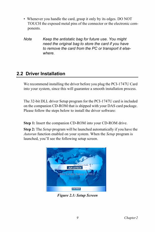
The 32-bit DLL driver Setup program for the PCI-1747U card is included on the companion CD-ROM that is shipped with your DAS card package. Please follow the steps below to install the driver software:
Step 1: Insert the companion CD-ROM into your CD-ROM drive.Step 2: The Setup program will be launched automatically if you have the Autorun function enabled on your system. When the Setup program is launched, youll see the following setup screen.
Figure 2.1: Setup Screen
Note Keep the antistatic bag for future use. You might need the original bag to store the card if you have to remove the card from the PC or transport it else-where.
9 Chapter 2
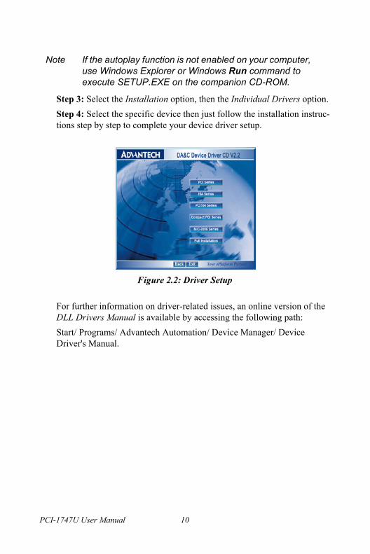
Step 3: Select the Installation option, then the Individual Drivers option.Step 4: Select the specific device then just follow the installation instruc-tions step by step to complete your device driver setup.
Figure 2.2: Driver Setup
For further information on driver-related issues, an online version of the DLL Drivers Manual is available by accessing the following path:Start/ Programs/ Advantech Automation/ Device Manager/ Device Driver's Manual.
Note If the autoplay function is not enabled on your computer, use Windows Explorer or Windows Run command to execute SETUP.EXE on the companion CD-ROM.
PCI-1747U User Manual 10
2.3 Hardware Installation
After the DLL driver installation is completed, you can go on to install the PCI-1747U card in any PCI slot on your computer. But it is suggested that you refer to the computer user manual or related documentations if you have any doubts. Please follow the steps below to install the card on your system:Step 1: Turn off your computer and unplug the power cord and cables. TURN OFF your computer before installing or removing any compo-nents on the computer.Step 2: Remove the cover of your computer.Step 3: Remove the slot cover on the back panel of your computer.Step 4: Touch the metal part on the surface of your computer to neutralize any static electricity that might be in your body.Step 5: Insert the PCI-1747U card into a PCI slot. Hold the card only by its edges and carefully align it with the slot. Insert the card firmly into place. Use of excessive force must be avoided; or the card might be dam-aged.Step 6: Fasten the bracket of the PCI card on the back panel rail of the computer with screws.Step 7: Connect appropriate accessories (68-pin cable, wiring terminals, etc. if necessary) to the PCI card.Step 8: Replace the cover of your computer chassis. Re-connect the cables you removed in step 2.Step 9: Plug in the power cord and turn on the computer.
Note Make sure you have installed the driver before you install the card (please refer to 2.2 Driver Installation)
11 Chapter 2
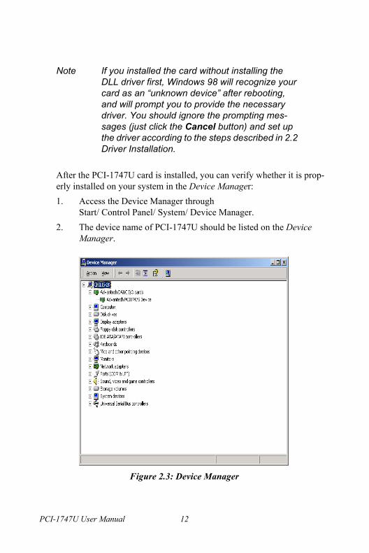
After the PCI-1747U card is installed, you can verify whether it is prop-erly installed on your system in the Device Manager:1. Access the Device Manager through
Start/ Control Panel/ System/ Device Manager.2. The device name of PCI-1747U should be listed on the Device
Manager.
Figure 2.3: Device Manager
Note If you installed the card without installing the DLL driver first, Windows 98 will recognize your card as an unknown device after rebooting, and will prompt you to provide the necessary driver. You should ignore the prompting mes-sages (just click the Cancel button) and set up the driver according to the steps described in 2.2 Driver Installation.
PCI-1747U User Manual 12
After your card is properly installed on your system, you can now config-ure your device using the Device Manager program that has itself already been installed on your system during driver setup. A complete device installation procedure should include device setup, configuration and test-ing. The following sections will guide you through the setup, configura-tion and testing of your device.
2.4 Device Setup & Configuration
The Device Manager program is a utility that allows you to set up, con-figure and test your device, and later stores your settings on the system registry. These settings will be used when you call the APIs of Advantech Device Drivers.
Set Up the DeviceStep 1: To install the I/O device for your card, you must first run the Device Installation program by accessing:Start/ Programs/ Advantech Automation/ Device Manager/ Advan-tech Device Manager.
Step 2: The Advantech Device Manager will search for the device(s) already installed on your system (if any) automatically.
Note If your card is properly installed, you should see the device name of your card listed on the Device Manager tab. If you see your device name listed, but marked with an exclamation sign !, it means your card has not been correctly installed. In this case, remove the card device from the Device Manager by selecting its device name and press the Remove button. Then go through the driver installation process again.
13 Chapter 2
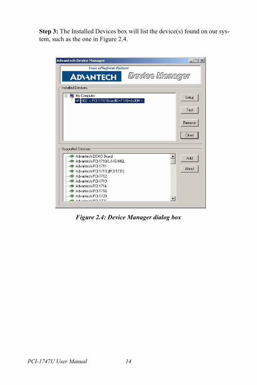
Step 3: The Installed Devices box will list the device(s) found on our sys-tem, such as the one in Figure 2.4.
Figure 2.4: Device Manager dialog box
PCI-1747U User Manual 14

Step 4: In the Device Setting dialog box (Figure2.5), you can configure the A/D channel as Single-ended or Differential.
Figure 2.5: Figure 2.5 The Device Setting dialog box
2.5 Auto-Calibration
This chapter provides brief information on PCI-1747U calibration. Regular calibration checks are important to maintain accuracy in data acquisition and control application. A calibration utility is included in the Device Manager.The PCI-1747U has been calibrated at the factory for initial use. However, a calibration of the analog input function every six months in recom-mended.
Note As we have noted, the device name "002 :< PCI-1747 BoardID=7 I/O=dc00H>" begins with a device number "002", which is specifically assigned to each card. The device number is passed to the driver to specify which device you wish to control.
15 Chapter 2
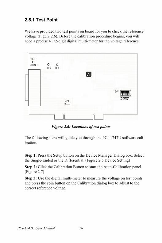
2.5.1 Test Point
We have provided two test points on board for you to check the reference voltage (Figure 2.6). Before the calibration procedure begins, you will need a precise 4 1/2-digit digital multi-meter for the voltage reference.
Figure 2.6: Locations of test points
The following steps will guide you through the PCI-1747U software cali-bration.
Step 1: Press the Setup button on the Device Manager Dialog box. Select the Single-Ended or the Differential. (Figure 2.5 Device Setting)Step 2: Click the Calibration Button to start the Auto-Calibration panel (Figure 2.7)Step 3: Use the digital multi-meter to measure the voltage on test points and press the spin button on the Calibration dialog box to adjust to the correct reference voltage.
PCI-1747U User Manual 16
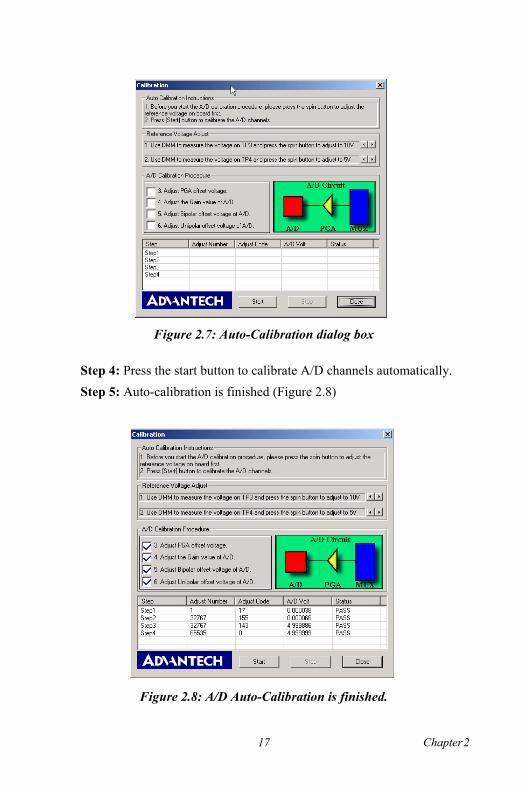
Figure 2.7: Auto-Calibration dialog box
Step 4: Press the start button to calibrate A/D channels automatically.Step 5: Auto-calibration is finished (Figure 2.8)
Figure 2.8: A/D Auto-Calibration is finished.
17 Chapter 2

2.6 Device Testing
Following through the Setup and Configuration procedures to the last step described in the previous section, you can now proceed to test the device by clicking the Test Button on the Device Manager Dialog box. A Device Test dialog box will appear accordingly(Figure 2.9):
Figure 2.9: Device Test dialog box
Only after your card device is properly set up, configured and tested, can the device installation procedure be counted as complete. After the device installation procedure is completed, you can safely proceed to the next chapter, Signal Connections.
PCI-1747U User Manual 18
2
CH
AP
TE
R 3Signal Connections
Maintaining signal connections is one of the most important factors in ensur-ing that your application system is sending and receiving data correctly. A good signal connection can avoid unnecessary and costly damage to your PC and other hardware devices. This chapter provides useful information about how to connect input and output signals to PCI-1747U via the I/O con-nector.Sections include:
I/O Connector Analog Input Connections Trigger Source Connections Field Wiring Considerations
Chapter 3 Signal Connections3.1 I/O Connector
The I/O connector on the PCI-1747U is a 68-pin connector that enables you to connect to accessories with the PCL-10168 shielded cable.
Fig. 3-1 shows the pin assignments for the 68-pin I/O connector on the PCI-1747U, and table 3-1 shows the I/O connector signal description.
3.1.1 I/O Connector Signal Description
Table 3.1: I/O Connector Signal Description
Signal Name Reference Direction Description
AI<0..63> AIGND Input Analog Input Channels 0 through 63. Each Channel pair,AI<i, i+1>( I = 0, 2, 462), can be configured as either two single-ended inputs or one differential input.
AGND -- -- Analog Input Ground. The ground reference is connected together on the PCI-1747U card.
PCI-1747U User Manual 20
3.1.2 Pin Assignment
Figure 3.1: I/O Connector Pin Assignments
21 Chapter 3
3.2 Analog Input Connections
3.2.1 Single-ended Channel Connections
The single-ended input configuration has only one signal wire for each channel, and the measured voltage (Vm) is the voltage of the wire as ref-erenced against the common ground.
A signal source without a local ground is also called a floating source. It is fairly simple to connect a single-ended channel to a floating signal source. In this mode, the PCI-1747U provides a reference ground for external floating signal sources. Fig. 3-2 shows a single-ended channel connection between a floating signal source and an input channel on PCI-1747U.
Figure 3.2: Single-ended Channel Connections
PCI-1747U User Manual 22

3.2.2 Differential Channel Connections
The differential input channels operate with two signal wires for each channel, and the voltage difference between both signal wires is mea-sured. On PCI-1747U, when all channels are configured to differential input, up to 32 analog channels are available.If one side of the signal source is connected to a local ground, the signal source is ground-referenced. Therefore, the ground of the signal source and the ground of the card will not be exactly of the same voltage. The difference between the ground voltages forms a common-mode voltage (V cm ).To avoid the ground loop noise effect caused by common-mode voltages, you can connect the signal ground to the Low input. Figure 3-3 shows a differential channel connection between a ground-reference signal source and an input channel on the PCI-1747U. With this connection, the PGIA rejects a common-mode voltage Vcm between the signal source and the PCI-1747U ground, shown as Vcm in Figure 3-3.
Figure 3.3: Differential Connection - Ground Signal
23 Chapter 3
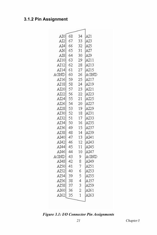
If a floating signal source is connected to the differential input channel, the signal source might exceed the common-mode signal range of the PGIA, and the PGIA will be saturated with erroneous voltage-readings. You must therefore reference the signal source against the AIGND.
Figure 3.4 shows a differential channel connection between a floating signal source and an input channel on PCI-1747U. In this figure, each side of the floating signal source is connected through a resistor to the AIGND. This connection can reject the common-mode voltage between the signal source and the PCI-1747U ground.
Figure 3.4: Differential Connection - Floating Signal
PCI-1747U User Manual 24
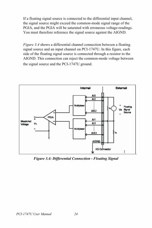
However, this connection has the disadvantage of loading the source down with the series combination (sum) of the two resistors. For ra and rb, for example, if the input impedance rs is 1 kW, and each of the two resistors are 100 kW, then the resistors load down the signal source with 200 kW (100 kW + 100 kW), resulting in a 0.5% gain error. The follow-ing gives a simplified representation of the circuit and calculating pro-cess.
Figure 3.5: Example
3.3 Trigger Source Connections
3.3.1 Internal Pacer Trigger ConnectionPCI-1747U includes one 82C54 compatible programmable Timer/Counter chip that provides three 16-bit counters connected to a 10 MHz clock, each designated specifically as Counter 0, Counter 1 and Counter 2. Counter 0 is a counter which counts events from an input channel. Counter 1 and Counter 2 are cascaded to create a 32-bit timer for pacer triggering. For detailed information, please refer to Appendix D.
25 Chapter 3
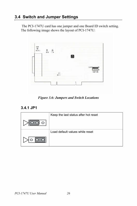
3.4 Switch and Jumper Settings
The PCI-1747U card has one jumper and one Board ID switch setting. The following image shows the layout of PCI-1747U:
Figure 3.6: Jumpers and Switch Locations
3.4.1 JP1
Keep the last status after hot reset
Load default values while reset
PCI-1747U User Manual 26

3.4.2 Board ID
Note: On: 1, Off: 0
ID3 ID2 ID1 ID0 Board ID
1 1 1 1 0
1 1 1 0 1
1 1 0 1 2
1 1 0 0 3
1 0 1 1 4
1 0 1 0 5
1 0 0 1 6
1 0 0 0 7
0 1 1 1 8
0 1 1 0 9
0 1 0 1 10
0 1 0 0 11
0 0 1 1 12
0 0 1 0 13
0 0 0 1 14
0 0 0 0 15
27 Chapter 3

PCI-1747U User Manual 28
2
CH
AP
TE
R 4Software Overview
This chapter gives you an overview of the software programming choices available and a quick reference to source codes examples that can help you be better informed when program-ming. After following the instructions given in Chapter 2, it is hoped that you feel comfortable enough to proceed fur-ther.Sections include:
Software Overview Programming Choices DLL Driver Programming
Chapter 4 Software Overview4.1 Software Overview
Programming choices for DAS cards: You may use Advantech applica-tion software such as Advantech DLL driver. On the other hand, advanced users are allowed another option for register-level program-ming, although not recommended due to its laborious and time-consum-ing nature.
4.2 Programming Choices
4.2.1 DLL Driver
The Advantech DLL Drivers software is included on the companion CD-ROM at no extra charge. It also comes with all the Advantech DAS cards. Advantechs DLL driver features a complete I/O function library to help boost your application performance. The Advantech DLL driver for Win-dows 98/2000/XP works seamlessly with development tools such as Visual C++, Visual Basic, Borland C++ Builder and Borland Delphi.
4.2.2 Register-Level Programming
Register-level programming is reserved for experienced programmers who find it necessary to write code directly at the level of device regis-ters. Since register-level programming requires much effort and time, we recommend that you use the Advantech DLL drivers instead. However, if register-level programming is indispensable, you should refer to the rele-vant information in Appendix C, Register Structure and Format, or to the example codes included on the companion CD-ROM.
PCI-1747U User Manual 30

4.3 DLL Driver Programming Roadmap
This section will provide you a roadmap to demonstrate how to build an application from scratch using Advantech DLL driver with your favorite development tools such as Visual C++, Visual Basic, Delphi and C++ Builder. The step-by-step instructions on how to build your own applica-tions using each development tool will be given in the DLL Drivers Man-ual. Moreover, a rich set of example source codes are also given for your reference.
4.3.1 Programming Tools
Programmers can develop application programs with their favorite devel-opment tools: Visual C++ Visual Basic Delphi C++ BuilderFor instructions on how to begin programming in each development tool, Advantech offers a Tutorial Chapter in the DLL Drivers Manual for your reference. Please refer to the corresponding sections in this chapter on the DLL Drivers Manual to begin your programming efforts. You can also take a look at the example source codes provided for each programming tool, since they can be very helpful.
The DLL Drivers Manual can be found on the companion CD-ROM. Or if you have already installed the DLL Drivers on your system, The DLL Drivers Manual can be readily accessed through the Start button:
Start/Programs/Advantech Automation/Device Manager/Device Driver's Manual
The example source codes can be found under the corresponding installa-tion folder such as the default installation path:
\Program Files\ADVANTECH\ADSAPI\Examples
31 Chapter 4

For information about using other function groups or other development tools, please refer to the Creating Windows 98/2000/XP Application with DLL Driver chapter and the Function Overview chapter on the DLL Driv-ers Manual.
4.3.2 Programming with DLL Driver Function Library
Advantech DLL driver offers a rich function library to be utilized in vari-ous application programs. This function library consists of numerous APIs that support many development tools, such as Visual C++, Visual Basic, Delphi and C++ Builder.
According to their specific functions or services, these APIs can be cate-gorized into several function groups: Analog Input Function Group Analog Output Function Group Digital Input/Output Function Group Counter Function Group Temperature Measurement Function Group Alarm Function Group Port Function Group Communication Function Group Event Function GroupFor the usage and parameters of each function, please refer to the Func-tion Overview chapter in the DLL Drivers Manual.
PCI-1747U User Manual 32
4.3.3 Troubleshooting DLL Driver Error
Driver functions will return a status code when they are called to perform a certain task for the application. When a function returns a code that is not zero, it means the function has failed to perform its designated func-tion. To troubleshoot the DLL driver error, you can pass the error code to DRV_GetErrorMessage function to return the error message. Or you can refer to the DLL Driver Error Codes Appendix in the DLL Drivers Manual for a detailed listing of the Error Code, Error ID and the Error Message.
33 Chapter 4

PCI-1747U User Manual 34

2
AP
PE
ND
IX ASpecifications
Sections include:
Analog Input General

Appendix A SpecificationsA.1 Analog Input
Channels 64 single-ended or 32 differential or combination
Resolution 16-bit
FIFO Size 1K samples
Max. Sampling Rate
250 kS/s
Input range and Gain List
Gain 0.5 1 2 4 8
Unipolar N/A 0~10 0~5 0~2.5 0~1.25
Bipolar ±10 ±5 ±2.5 ±1.25 ±0.625
Bandwidth for PGA (MHz)
Gain 0.5 1 2 4 8
Bandwidth 4.0 4.0 2.0 1.5 0.65
Common mode voltage
±11 V max. (operational)
Max. Input voltage ±20 V
Input Impedance 100 MΩ/10pF(Off); 100 MΩ/100pF(On)
Accuracy DC DNLE: ±1LSB
INLE: ±1LSB
Zero (Offset) error: Adjustable to ±2 LSB
Gain 0.5 1 2 4 8
Gain error(% FSR)
0.03 0.02 0.02 0.03 0.04
AC THD: -90 dB
ENOB: 13.5 bits
Clocking and Trig-ger Inputs
Trig-ger Mode
Software, on-board programmable pacer
A/D pacer clock
250 kHz (max.); 2.328mHz (min.)
PCI-1747U User Manual 36
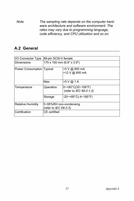
A.2 General
Note The sampling rate depends on the computer hard-ware architecture and software environment. The rates may vary due to programming language, code efficiency, and CPU utilization and so on.
I/O Connector Type 68-pin SCSI-II femaleDimensions 175 x 100 mm (6.9" x 3.9")
Power Consumption Typical +5 V @ 850 mA+12 V @ 600 mA
Max. +5 V @ 1 A
Temperature Operation 0~+60°C(32~158°F) (refer to IEC 68-2-1,2)
Storage -20~+85°C(-4~185°F)
Relative Humidity 5~95%RH non-condensing (refer to IEC 68-2-3)
Certification CE certified
37 Appendix A

PCI-1747U User Manual 38
2
AP
PE
ND
IX BBlock Diagram
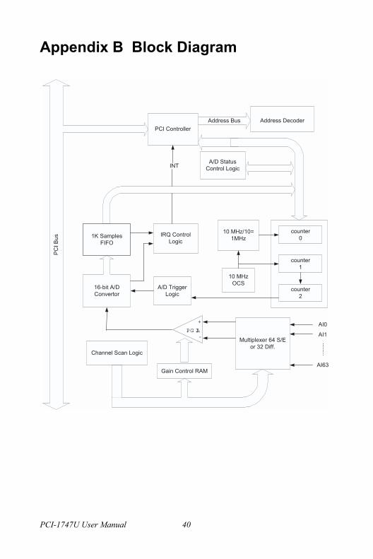
PCI-1747U User Manual 40
Appendix B Block DiagramP
CI B
us
PCI ControllerAddress Decoder
1K SamplesFIFO
A/D StatusControl Logic
16-bit A/DConvertor
IRQ ControlLogic
counter0
counter1
counter2
10 MHz/10=1MHz
10 MHzOCS
A/D TriggerLogic
Channel Scan Logic
Multiplexer 64 S/Eor 32 Diff.
Gain Control RAM
PG IA
+
-
Address Bus
INT
AI0
AI1
AI63
......
..
2
AP
PE
ND
IX CRegister Structure and Format
Appendix C Register Structure and For-mat
C.1 Overview
PCI-1747U is delivered with an easy-to-use 32-bit DLL driver for user programming under the Windows 98/2000/XP operating systems. We rec-ommend to program the PCI-1747U using the 32-bit DLL driver pro-vided by Advantech to avoid the complexity of low-level programming by registers.
The most important consideration in programming the PCI-1747U at the register level is to understand the function of the card's registers. The information in the following sections is provided only for users who would like to do their own low-level programming.
C.2 I/O Port Address Map
PCI-1747U requires 32 consecutive addresses in the PC's I/O space. The address of each register is specified as an offset from the card's base address. For example, BASE+0 is the card's base address and BASE+7 is the base address plus seven bytes.
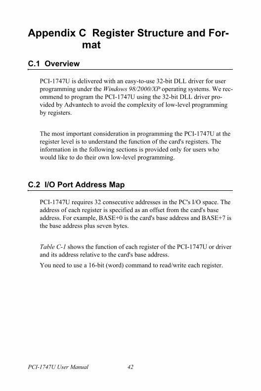
Table C-1 shows the function of each register of the PCI-1747U or driver and its address relative to the card's base address.You need to use a 16-bit (word) command to read/write each register.
PCI-1747U User Manual 42

Table C.1: PCI-1747U Register Format (Part 1)BaseAddress+decimal
Read
7 6 5 4 3 2 1 0
A/D Data
1 AD15 AD14 AD13 AD12 AD11 AD10 AD9 AD8
0 AD7 AD6 AD5 AD4 AD3 AD2 AD1 AD0
N/A
3
2
N/A
5
4
A/D Status Register
7 CAL ADIRQ
F/F F/H F/E
6 ONE/FH
IRQEN PACER
SW
N/A
9
8
N/A
11
10
N/A
13
12
N/A
15
14
43 Appendix C
BaseAddress+decimal
Read
7 6 5 4 3 2 1 0
N/A
17
16
N/A
19
18
Board ID
21
20 BD3 BD2 BD1 BD0
N/A
23
22
Counter 0
25
24 D7 D6 D5 D4 D3 D2 D1 D0
Counter 1
27
26 D7 D6 D5 D4 D3 D2 D1 D0
Counter 2
29
28 D7 D6 D5 D4 D3 D2 D1 D0
Counter Control
31
30 D7 D6 D5 D4 D3 D2 D1 D0
PCI-1747U User Manual 44

BaseAddress+decimal
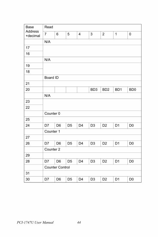
Write
7 6 5 4 3 2 1 0
Software A/D Trigger
1
0
A/D Channel Range Setting
3
2 S/D B/U G2 G1 G0
Multiplexer Control
5 STO5 STO4 STO3 STO2 STO1 STO0
4 STA5 STA4 STA3 STA2 STA1 STA0
A/D Control Register
7 CAL
6 ONE/FH
ADIRQEN
PACER SW
Clear Interrupt and FIFO
9 Clear FIFO
8 Clear interrupt
N/A
11
10
N/A
13
12
N/A
15
14
45 Appendix C
BaseAddress+decimal
Write
7 6 5 4 3 2 1 0
N/A
17
16
Calibration Command and Data
19 CM3 CM2 CM1 CM0
18 D7 D6 D5 D4 D3 D2 D1 D0
N/A
21
20
N/A
23
22
Counter 0
25
24 D7 D6 D5 D4 D3 D2 D1 D0
Counter 1
27
26 D7 D6 D5 D4 D3 D2 D1 D0
Counter 2
29
28 D7 D6 D5 D4 D3 D2 D1 D0
Counter Control
31
30 D7 D6 D5 D4 D3 D2 D1 D0
PCI-1747U User Manual 46

C.3 A/D Data BASE+0 and BASE+1
BASE+0 and BASE+1 hold the result of A/D conversion data. The 16 bits of data from the A/D conversion are stored in BASE+1 bit 7 to bit 0 and BASE+0 bit 7 to bit 0.
AD15 ~ AD0 Result of A/D ConversionAD0 the least significant bit (LSB) of A/D dataAD15the most significant bit (MSB)
C.4 Software A/D Trigger BASE+0
You can trigger an A/D conversion by software, the card's on-board pacer.
BASE+6, Bit 2 to bit 0, select the trigger source.(see Section C.7, Control Register -- BASE+6 )
If you select software triggering, a write to the register BASE+0 with any value will trigger an A/D conversion.
Table C.2: PCI-1747U Register for A/D data
Read A/D Data
Bit # 7 6 5 4 3 2 1 0
BASE + 1 AD15 AD14 AD13 AD12 AD11 AD10 AD9 AD8
BASE + 0 AD7 AD6 AD5 AD4 AD3 AD2 AD1 AD0
47 Appendix C
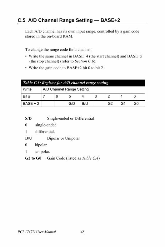
C.5 A/D Channel Range Setting BASE+2
Each A/D channel has its own input range, controlled by a gain code stored in the on-board RAM.
To change the range code for a channel: Write the same channel in BASE+4 (the start channel) and BASE+5
(the stop channel) (refer to Section C.6). Write the gain code to BASE+2 bit 0 to bit 2.
S/D Single-ended or Differential0 single-ended1 differential.B/U Bipolar or Unipolar0 bipolar1 unipolar.G2 to G0 Gain Code (listed as Table C.4)
Table C.3: Register for A/D channel range settingWrite A/D Channel Range Setting
Bit # 7 6 5 4 3 2 1 0
BASE + 2 S/D B/U G2 G1 G0
PCI-1747U User Manual 48

Example: To set channel 3 as gain=11. Write channel 3 to BASE+4 as 00000011.2. Write channel 3 to BASE+5 as 00000011.3. Refer to the gain code list, write gain=1 to BASE+2 as 00000000.
Table C.4: Gain codes for PCI-1747UGain Input Range(V) B/U Gain Code
G2 G1 G0
1 -5 to +5 0 0 0 0
2 -2.5 to +2.5 0 0 0 1
4 -1.25 to +1.25 0 0 1 0
8 -0.625 to +0.625 0 0 1 1
0.5 -10 to +10 0 1 0 0
N/A 0 1 0 1
N/A 0 1 1 0
N/A 0 1 1 1
1 0 to 10 1 0 0 0
2 0 to 5 1 0 0 1
4 0 to 2.5 1 0 1 0
8 0 to 1.25 1 0 1 1
N/A 1 1 0 0
N/A 1 1 0 1
N/A 1 1 1 0
N/A 1 1 1 1
49 Appendix C
C.6 MUX Control BASE+4 and BASE+5
STA5 ~ STA0 Start Scan Channel NumberSTO5 ~ STO0 Stop Scan Channel Number When you set the gain code of analog input channel n, you should set
the Multiplexer start & stop channel number to channel n to prevent any unexpected errors. In fact BASE+4 bit 5 to bit 0, STA5 ~ STA0, act as a pointer to channel ns address in the SRAM when you program the A/D channel setting (refer to Section C.5).
The write-only registers of BASE +4 and BASE+5 control how the multi-plexers (Multiplexer) scan. BASE+4 bit 5 to bit 0, STA5 ~ STA0, hold the start scan ch. number. BASE+5 bit 5 to bit 0, STO5 ~ STO0, hold the stop scan ch. number.Writing to these two registers automatically initializes the scan range of the Multiplexer. Each A/D conversion trigger also sets the Multiplexer to the next channel. With continuous triggering, the Multiplexer will scan from the start channel to the stop channel and then repeat. The following examples show the scan sequences of the Multiplexer.
Table C.5: Register for multiplexer controlWrite Multiplexer Control
Bit # 7 6 5 4 3 2 1 0
BASE + 5 STO5 STO4 STO3 STO2 STO1 STO0
BASE + 4 STA5 STA4 STA3 STA2 STA1 STA0
Caution! We recommend you to set the same start and stop channel when writing to the register BASE+2. Otherwise, if the A/D trigger source is on, the mul-tiplexer will continuously scan between channels and the range setting may be set to an unex-pected channel. Make sure the A/D trigger source is turned off to avoid this kind of error.
PCI-1747U User Manual 50

C.6.1 Example 1
If the start scan input channel is AI3 and the stop scan input channel is AI7, then the scan sequence is AI3, AI4, AI5, AI6, AI7, AI3, AI4, AI5, AI6, AI7, AI3, AI4
C.6.2 Example 2
If the start scan channel is AI13 and the stop scan channel is AI2, then the scan sequence is AI13, AI14...AI63, AI0, AI1, AI2.
The scan logic of the PCI-1747U card is powerful and easily understood. You can set the gain code, B/U and S/D, for each channel. For the Analog Input function, we set two AI channels AI<i, i+1> ( i= 0, 2, 4, ..., 62) to work as a pair. For example, AI0 and AI1 is a pair. When in single-ended mode, we can get data from AI0 and AI1 separately. But if we set them in differential mode, the results polling AI0 and AI1 will be the same. That is if we set AI0 and AI1 as differential input channels, we can get the cor-rect result no matter if we poll channel 0 or channel 1.
51 Appendix C
But if we want to use the multiple channels input function, things will be a bit different. If we set two AI channels as differential channels, it will take one channel in the data array. Since the resulted data array of the multi-channel scan function is ranked with the order of channel, let us give an example to make it more clear. Now we set channel 0, 1 as differ-ential and 2, 3 as single ended and then 4, 5 in differential mode. And we set the start channel as channel 0 and number of channels as 4, the result will be:
##.#### -> channel 0,1##.#### -> channel 2##.#### -> channel 3##.#### -> channel 4,5##.#### -> channel 0,1##.#### -> channel 2##.#### -> channel 3##.#### -> channel 4,5##.#### -> channel 0,1
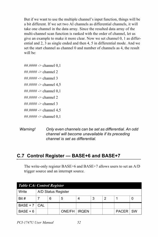
C.7 Control Register BASE+6 and BASE+7
The write-only register BASE+6 and BASE+7 allows users to set an A/D trigger source and an interrupt source.
Warning! Only even channels can be set as differential. An odd channel will become unavailable if its preceding channel is set as differential.
Table C.6: Control RegisterWrite A/D Status Register
Bit # 7 6 5 4 3 2 1 0
BASE + 7 CAL
BASE + 6 ONE/FH IRQEN PACER SW
PCI-1747U User Manual 52
SW Software trigger enable bit1 enable0 disable.PACER Pacer trigger enable bit1 enable0 disable.
IRQEN Interrupt enable bit.0 Disable1 Enable
ONE/FH Interrupt source bit0 Interrupt when an A/D conversion occurs1 Interrupt when the FIFO is half full.CAL Analog calibration bit0 Normal modeAll analog input channels are connected to 68 pin SCSI-II connector respectively.1 Calibration mode
The wiring becomes that AI0, 2, 4, 6 are connected to 0 V (AGND), AI1 is connected to +10V, AI3 is connected to +5V, AI5 is connected to +2.5V, and AI7 is connecter to +1.25V automatically.
Note: Users cannot enable SW and PACER concurrently.
53 Appendix C

C.8 Status Register BASE+6 and BASE+7
The registers of BASE+6 and BASE+7 provide information for A/D con-figuration and operation.
The content of the status register of BASE+6 is the same as that of the control register.F/E FIFO Empty flagThis bit indicates whether the FIFO is empty.1 means that the FIFO is empty.F/H FIFO Half-full flagThis bit indicates whether the FIFO is half-full.1 means that the FIFO is half-full.F/F FIFO Full flagThis bit indicates whether the FIFO is full.1 means that the FIFO is full.IRQ Interrupt flagThis bit indicates the interrupt status.1 means that an interrupt has occurred.
Table C.7: Status RegisterWrite A/D Status Register
Bit # 7 6 5 4 3 2 1 0
BASE + 7 CAL IRQ F/F F/H F/E
BASE + 6 ONE/FH IRQEN PACER SW
PCI-1747U User Manual 54
C.9 Clear Interrupt and FIFO BASE+8 and BASE+9
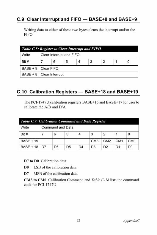
Writing data to either of these two bytes clears the interrupt and/or the FIFO.
C.10 Calibration Registers BASE+18 and BASE+19
The PCI-1747U calibration registers BASE+16 and BASE+17 for user to calibrate the A/D and D/A.
D7 to D0 Calibration dataD0 LSB of the calibration dataD7 MSB of the calibration dataCM3 to CM0 Calibration Command and Table C-18 lists the command code for PCI-1747U
Table C.8: Register to Clear Interrupt and FIFOWrite Clear Interrupt and FIFO
Bit # 7 6 5 4 3 2 1 0
BASE + 9 Clear FIFO
BASE + 8 Clear Interrupt
Table C.9: Calibration Command and Data RegisterWrite Command and Data
Bit # 7 6 5 4 3 2 1 0
BASE + 19 CM3 CM2 CM1 CM0
BASE + 18 D7 D6 D5 D4 D3 D2 D1 D0
55 Appendix C
C.10.1 Calibration Procedure:
1.Adjust 10V reference: use DMM to measure the voltage on TP3 and adjust to 10.0000V2.Adjust 5V reference: use DMM to measure the voltage on TP4 and adjust to 5.00000V3.PGA offset adjust:4.Bipolar offset adjust:5.Unipolar offset adjust:6.Gain adjust:
Table C.10: Calibration Command and Data RegisterMeaning/Command Code CM3 CM2 CM1 CM0
PGA offset adjust (Coarse) 0 0 0 0
PGA offset adjust (Fine) 0 0 0 1
A/D bipolar offset adjust (Coarse) 0 0 1 0
A/D bipolar offset adjust (Fine) 0 0 1 1
A/D unipolar offset adjust (Coarse) 0 1 0 0
A/D unipolar offset adjust (Fine) 0 1 0 1
A/D gain adjust (Coarse) 0 1 1 0
A/D gain adjust (Fine) 0 1 1 1
10V reference adjust 1 0 0 0
5V reference adjust 1 0 0 1
PCI-1747U User Manual 56
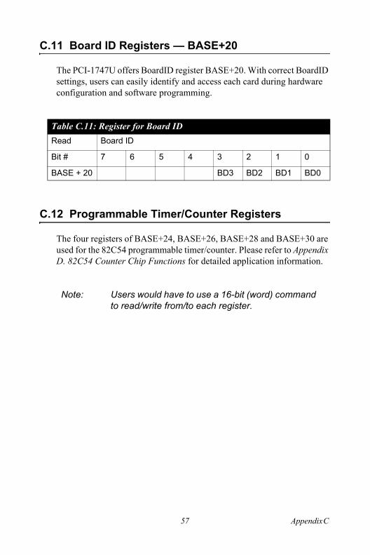
C.11 Board ID Registers BASE+20
The PCI-1747U offers BoardID register BASE+20. With correct BoardID settings, users can easily identify and access each card during hardware configuration and software programming.
C.12 Programmable Timer/Counter Registers
The four registers of BASE+24, BASE+26, BASE+28 and BASE+30 are used for the 82C54 programmable timer/counter. Please refer to Appendix D. 82C54 Counter Chip Functions for detailed application information.
Table C.11: Register for Board IDRead Board ID
Bit # 7 6 5 4 3 2 1 0
BASE + 20 BD3 BD2 BD1 BD0
Note: Users would have to use a 16-bit (word) command to read/write from/to each register.
57 Appendix C

PCI-1747U User Manual 58
2
AP
PE
ND
IX D82C54 Counter Chip Function
Sections Include:
The Intel 82C54 Counter Read/Write and Control
Registers
Appendix D 82C54 Counter Chip Func-tion
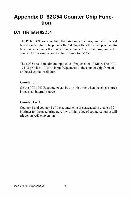
D.1 The Intel 82C54
The PCI-1747U uses one Intel 82C54-compatible programmable interval timer/counter chip. The popular 82C54 chip offers three independent 16-bit counters, counter 0, counter 1 and counter 2. You can program each counter for maximum count values from 2 to 65535.
The 82C54 has a maximum input clock frequency of 10 MHz. The PCI-1747U provides 10 MHz input frequencies to the counter chip from an on-board crystal oscillator.
Counter 0On the PCI-1747U, counter 0 can be a 16-bit timer when the clock source is set as an internal source.
Counter 1 & 2Counter 1 and counter 2 of the counter chip are cascaded to create a 32-bit timer for the pacer trigger. A low-to-high edge of counter 2 output will trigger an A/D conversion.
PCI-1747U User Manual 60
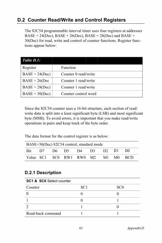
D.2 Counter Read/Write and Control Registers
The 82C54 programmable interval timer uses four registers at addresses BASE + 24(Dec), BASE + 26(Dec), BASE + 28(Dec) and BASE + 30(Dec) for read, write and control of counter functions. Register func-tions appear below:
Since the 82C54 counter uses a 16-bit structure, each section of read/write data is split into a least significant byte (LSB) and most significant byte (MSB). To avoid errors, it is important that you make read/write operations in pairs and keep track of the byte order.
The data format for the control register is as below:
D.2.1 Description
Table D.1:
Register FunctionBASE + 24(Dec) Counter 0 read/writeBASE + 26(Dec Counter 1 read/writeBASE + 28(Dec) Counter 1 read/writeBASE + 30(Dec) Counter control word
BASE+30(Dec) 82C54 control, standard modeBit D7 D6 D5 D4 D3 D2 D1 D0
Value SC1 SC0 RW1 RW0 M2 M1 M0 BCD
SC1 & SC0 Select counter
Counter SC1 SC00 0 01 0 12 1 0Read-back command 1 1
61 Appendix D
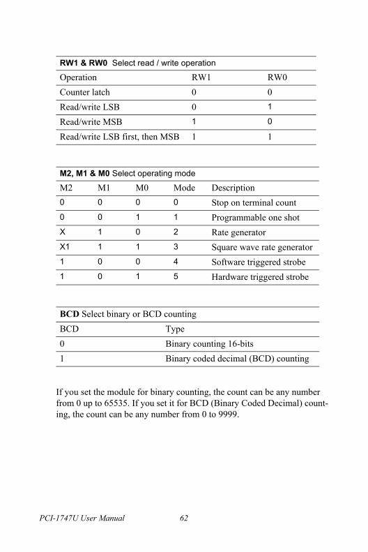
If you set the module for binary counting, the count can be any number from 0 up to 65535. If you set it for BCD (Binary Coded Decimal) count-ing, the count can be any number from 0 to 9999.
RW1 & RW0 Select read / write operation
Operation RW1 RW0Counter latch 0 0Read/write LSB 0 1
Read/write MSB 1 0
Read/write LSB first, then MSB 1 1
M2, M1 & M0 Select operating mode
M2 M1 M0 Mode Description0 0 0 0 Stop on terminal count0 0 1 1 Programmable one shotX 1 0 2 Rate generatorX1 1 1 3 Square wave rate generator1 0 0 4 Software triggered strobe1 0 1 5 Hardware triggered strobe
BCD Select binary or BCD countingBCD Type0 Binary counting 16-bits1 Binary coded decimal (BCD) counting
PCI-1747U User Manual 62

If you set both SC1 and SC0 bits to 1, the counter control register will be in read-back command mode. The control register data format then becomes:
CNT = 0 Latch count of selected counter(s)STA = 0 Latch status of selected counter(s)C2, C1 & C0 Select counter for a read-back operationC2 = 1 select Counter 2C1 = 1 select Counter 1C0 = 1 select Counter 0
If you set both SC1 and SC0 to 1 and STA to 0, the register selected by C2 to C0 contains a byte which shows the status of the counter. The data format of the counter read/write register then becomes:
OUT Current state of counter outputNC Null count is 1 when the last count written to the counter register has been loaded into the counting element
BASE + 30(Dec) 82C54 control, read-back modeBit D7 D6 D5 D4 D3 D2 D1 D0Value 1 1 CNT STA C2 C1 C0 X
BASE+24/26/28(Dec) Status read-back modeBit D7 D6 D5 D4 D3 D2 D1 D0Value OUT NC RW1 RW0 M2 M1 M0 BCD
63 Appendix D
D.3 Counter Operating Modes
The 82C54 programmable interval timer uses four registers at addresses BASE + 24(Dec), BASE + 26(Dec), BASE + 28(Dec) and BASE + 30(Dec) for read, write and control of counter functions. Register func-tions appear below:
MODE 0 - Stop on Terminal Count
The output will initially below after you set operation to this mode. After you load the count into the selected count register, the output will remain low and the counter will count. When the counter reaches the terminal count, its output will go high and remain high until you reload it with the mode or a new count value. The counter continues to decrement after it reaches the terminal count. Rewriting a counter register during counting has the following results:
1. Writing to the first byte stops the current counting.2. Writing to the second byte starts the new count.
MODE 1 - Programmable One-shot Pulse
The output is initially high. The output will go low on the count following the rising edge of the gate input. It will then go high on the terminal count. If you load a new count value while the output is low, the new value will not affect the duration of the one-shot pulse until the succeed-ing trigger. You can read the current count at any time without affecting the one-shot pulse. The one-shot is re-triggerable, thus the output will remain low for the full count after any rising edge at the gate input.
MODE 2 - Rate Generator
The output will be low for one period of the input clock. The period from one output pulse to the next equals the number of input counts in the counter register. If you reload the counter register between output pulses,
PCI-1747U User Manual 64
the present period will not be affected, but the subsequent period will reflect the value.The gate input, when low, will force the output high. When the gate input goes high, the counter will start from the initial count. You can thus use the gate input to synchronize the counter.
With this mode the output will remain high until you load the count regis-ter. You can also synchronize the output by software.
MODE 3 - Square Wave Generator
This mode is similar to Mode 2, except that the output will remain high until one half of the count has been completed (for even numbers), and will go low for the other half of the count. This is accomplished by decreasing the counter by two on the falling edge of each clock pulse. When the counter reaches the terminal count, the state of the output is changed, the counter is reloaded with the full count and the whole process is repeated.
If the count is odd and the output is high, the first clock pulse (after the count is loaded ) decrements the count by 1. Subsequent clock pulses dec-rement the count by 2. After time-out, the output goes low and the full count is reloaded. The first clock pulse (following the reload) decrements the counter by 3. Subsequent clock pulses decrement the count by two until time-out, then the whole process is repeated. In this way, if the count is odd, the output will be high for (N+1)/2 counts and low for (N-1)/2 counts.
MODE 4 -Software-Triggered Strobe
After the mode is set, the output will be high. When the count is loaded, the counter will begin counting. On terminal count, the output will go low for one input clock period then go high again. If you reload the count reg-ister during counting, the new count will be loaded on the next CLK pulse. The count will be inhibited while the GATE input is low.
65 Appendix D

MODE 5 - Hardware-Triggered Strobe
The counter will start counting after the rising edge of the trigger input and will go low for one clock period when the terminal count is reached. The counter is re-triggerable.
PCI-1747U User Manual 66