256 10 device family pin connection guidelines - intel.com · intel® stratix® 10 gx pin...
TRANSCRIPT

Intel® Stratix® 10 Device Family Pin ConnectionGuidelines
SubscribeSend Feedback
PCG-01020 | 2018.08.16Latest document on the web: PDF | HTML
Contents
Intel® Stratix® 10 Device Family Pin Connection Guidelines.......................................................................................................4Intel® Stratix® 10 GX Pin Connection Guidelines..................................................................................................................... 5
Clock and PLL Pins..................................................................................................................................................... 5Dedicated Configuration/JTAG Pins............................................................................................................................... 6Optional/Dual-Purpose Configuration Pins......................................................................................................................83V Compatible I/Os....................................................................................................................................................9Differential I/O Pins..................................................................................................................................................10External Memory Interface Pins..................................................................................................................................10Voltage Sensor Pins..................................................................................................................................................11Temperature Sensor Pins...........................................................................................................................................12Reference Pins.........................................................................................................................................................13No Connect and DNU Pins......................................................................................................................................... 14Power Supply Pins....................................................................................................................................................14Transceiver Pins.......................................................................................................................................................19Secure Device Manager (SDM) Pins............................................................................................................................ 22Notes to Intel Stratix 10 GX Pin Connection Guidelines..................................................................................................32
Intel Stratix 10 MX Pin Connection Guidelines....................................................................................................................... 33UIB and eSRAM Pins.................................................................................................................................................33Intel Stratix 10 MX Power Supply Pins.........................................................................................................................35Notes to Intel Stratix 10 MX Pin Connection Guidelines..................................................................................................35
Intel Stratix 10 TX Pin Connection Guidelines........................................................................................................................ 36Intel Stratix 10 TX Transceiver Pins............................................................................................................................ 37Notes to Intel Stratix 10 TX Pin Connection Guidelines.................................................................................................. 39
Intel Stratix 10 SX Pin Connection Guidelines........................................................................................................................40Hard Processor System (HPS) Supply Pins................................................................................................................... 40HPS Oscillator Clock Input Pin....................................................................................................................................42HPS JTAG Pins......................................................................................................................................................... 42HPS GPIO Pins.........................................................................................................................................................43HPS SDMMC Pins..................................................................................................................................................... 44HPS NAND Pins........................................................................................................................................................45HPS USB Pins.......................................................................................................................................................... 47HPS EMAC Pins........................................................................................................................................................ 48
Contents
Intel® Stratix® 10 Device Family Pin Connection Guidelines2

HPS I2C_EMAC and MDIO Pins...................................................................................................................................50HPS I2C Pins........................................................................................................................................................... 51HPS SPI Pins........................................................................................................................................................... 52HPS UART Pins.........................................................................................................................................................54HPS Trace Pins.........................................................................................................................................................55Notes to Intel Stratix 10 SX Pin Connection Guidelines.................................................................................................. 57
Power Supply Sharing Guidelines for Intel Stratix 10 Devices.................................................................................................. 58Example 1—Intel Stratix 10 GX..................................................................................................................................59Example 2—Intel Stratix 10 GX..................................................................................................................................62Example 3—Intel Stratix 10 SX (–1V, –2V, and –3V parts)............................................................................................. 65Example 4—Intel Stratix 10 SX (–2L and –3X parts)..................................................................................................... 68Example 5—Intel Stratix 10 SX (–1V, –2V, and –3V parts)............................................................................................. 71Example 6—Intel Stratix 10 SX (–2L and –3X parts)..................................................................................................... 74Example 7—Intel Stratix 10 MX (–1V, –2V, and –3V parts).............................................................................................77Example 8—Intel Stratix 10 MX (–2L and –3X parts).....................................................................................................81Example 9—Intel Stratix 10 MX (–1V, –2V, and –3V parts).............................................................................................85Example 10—Intel Stratix 10 MX (–2L and –3X parts)................................................................................................... 89Example 11—Intel Stratix 10 TX (–1V, –2V, and –3V parts)............................................................................................92Example 12—Intel Stratix 10 TX (–2L and –3X parts)....................................................................................................96
Document Revision History for the Intel Stratix 10 Device Family Pin Connection Guidelines...................................................... 100
Contents
Intel® Stratix® 10 Device Family Pin Connection Guidelines3

Intel® Stratix® 10 Device Family Pin Connection Guidelines
Disclaimer© 2018 Intel Corporation. All rights reserved. Intel, the Intel logo, Altera, Arria, Cyclone, Enpirion, MAX, Megacore, NIOS, Quartus Prime and Stratix words and logos aretrademarks of Intel Corporation in the US and/or other countries. Other marks and brands may be claimed as the property of others. Intel warrants performance of its FPGAand semiconductor products to current specifications in accordance with Intel's standard warranty, but reserves the right to make changes to any products and services atany time without notice. Intel assumes no responsibility or liability arising out of the application or use of any information, product, or service described herein except asexpressly agreed to in writing by Intel. Intel customers are advised to obtain the latest version of device specifications before relying on any published information andbefore placing orders for products or services.
These pin connection guidelines, and your use thereof, are subject to and governed by Intel’s terms and conditions below. By using these pin connection guidelines, youindicate your acceptance of all such terms and conditions. If you do not agree with such terms and conditions, you may not use the pin connection guidelines, and you arerequired to promptly and irrevocably destroy the pin connection guidelines and any copies or portions thereof in your possession or under your control.
Terms and Conditions:
1. These pin connection guidelines are provided as examples only, and should not be deemed to be technical specifications or recommendations. The use of the pin connection guidelines for any particular design should be verified for device operation with the applicable datasheet and Intel.2. Subject to these terms and conditions, Intel grants to you the use of these pin connection guidelines as examples of possible pin connections of an Intel programmable logic device-based design. You may not use these pin connection guidelines for any other purpose except as expressly permitted in these terms and conditions. Intel does not recommend, suggest, or require that these pin connection guidelines be used in conjunction or combination with any other software or product, and makes no representations, warranties or guaranties, implied or express as well as any warranties arising from course of performance, course of dealing, or usage in trade including but not limited to the accuracy, completeness or genuineness thereof.3. Intel will not be liable for any lost revenue, lost profits, or other consequential, indirect, or special damages caused by your use of these pin connection guidelines even if advised of the possibility of such damages occurring.4. This agreement shall be governed in all respects by the laws of the State of Delaware, without regard to conflict of law or choice of law principles. You agree to submit to the exclusive jurisdiction of the federal and state courts in the State of Delaware for the resolution of any dispute or claim arising out of or relating to these terms of use.
PCG-01020 | 2018.08.16
Intel Corporation. All rights reserved. Intel, the Intel logo, Altera, Arria, Cyclone, Enpirion, MAX, Nios, Quartus and Stratix words and logos are trademarks of IntelCorporation or its subsidiaries in the U.S. and/or other countries. Intel warrants performance of its FPGA and semiconductor products to current specifications inaccordance with Intel's standard warranty, but reserves the right to make changes to any products and services at any time without notice. Intel assumes noresponsibility or liability arising out of the application or use of any information, product, or service described herein except as expressly agreed to in writing byIntel. Intel customers are advised to obtain the latest version of device specifications before relying on any published information and before placing orders forproducts or services.*Other names and brands may be claimed as the property of others.
ISO9001:2015Registered
Intel® Stratix® 10 GX Pin Connection Guidelines
Clock and PLL Pins
Note: Intel recommends that you create an Intel® Quartus® Prime design, enter your device I/O assignments, and compile thedesign. The Intel Quartus Prime software will check your pin connections according to I/O assignment and placement rules.The rules differ from one device to another based on device density, package, I/O assignments, voltage assignments, andother factors that are not fully described in this document or the device handbook.
Table 1. Clock and PLL Pins—Preliminary
Pin Name PinFunctions
Pin Description Connection Guidelines
CLK_[2][A,B,C,F,G,H,I,J,K,L,M,N]_[0,1]p
CLK_[3][A,B,C,D,E,F,G,H,I,J,K,L]_[0,1]p
I/O, ClockInput
Dedicated high speed clock input pins that can be used fordata inputs or outputs. Differential input OCT Rd, single-ended input OCT Rt, and single-ended output OCT Rs aresupported on these pins.When you do not use these pins as dedicated clock pins, youcan use them as regular I/O pins.
Tie the unused pins to GND or leave them unconnected. Ifthe pins are not connected, use the Intel Quartus Primesoftware programmable options to internally bias these pins.These pins can be reserved as inputs tristate with weakinternal pull-up resistor enabled, or as outputs driving GND.
CLK_[2][A,B,C,F,G,H,I,J,K,L,M,N]_[0,1]n
CLK_[3][A,B,C,D,E,F,G,H,I,J,K,L]_[0,1]n
I/O, ClockInput
PLL_[2][A,B,C,F,G,H,I,J,K,L,M,N]_FB[0]
PLL_[3][A,B,C,F,G,H,I,J,K,L]_FB[0]
I/O, Clock Dual-purpose I/O pins that can be used as single-endedinputs, single-ended outputs, or external feedback input pins.For more information about the supported pins, refer to thedevice pin-out file.
Tie the unused pins to GND or leave them unconnected. Ifthe pins are not connected, use the Intel Quartus Primesoftware programmable options to internally bias these pins.These pins can be reserved as inputs tristate with weakinternal pull-up resistor enabled, or as outputs driving GND.
PLL_[2][A,B,C,F,G,H,I,J,K,L,M,N]_FBp
I/O, Clock Dual-purpose I/O pins that can be used as differential I/Os,or external feedback input pins.For more information about the supported pins, refer to thedevice pin-out file.
Tie the unused pins to GND or leave them unconnected. Ifthe pins are not connected, use the Intel Quartus Primesoftware programmable options to internally bias these pins.
continued...
Intel® Stratix® 10 Device Family Pin Connection Guidelines
PCG-01020 | 2018.08.16
Intel® Stratix® 10 Device Family Pin Connection Guidelines5

Pin Name PinFunctions
Pin Description Connection Guidelines
PLL_[3][A,B,C,F,G,H,I,J,K,L]_FBp
PLL_[2][A,B,C,F,G,H,I,J,K,L,M,N]_FBn
PLL_[3][A,B,C,F,G,H,I,J,K,L]_FBn
I/O, Clock
PLL_[2][A,B,C,F,G,H,I,J,K,L,M,N]_CLKOUT[0:1]
PLL_[3][A,B,C,F,G,H,I,J,K,L]_CLKOUT[0:1]
PLL_[2][A,B,C,F,G,H,I,J,K,L,M,N]_CLKOUT[0:1]p
PLL_[3][A,B,C,F,G,H,I,J,K,L]_CLKOUT[0:1]p
I/O, Clock I/O pins that can be used as two single-ended clock outputpins or one differential clock output pair.For more information about the supported pins, refer to thedevice pin-out file.
Tie the unused pins to GND or leave them unconnected. Ifthe pins are not connected, use the Intel Quartus Primesoftware programmable options to internally bias these pins.These pins can be reserved as inputs tristate with weakinternal pull-up resistor enabled, or as outputs driving GND.
PLL_[2][A,B,C,F,G,H,I,J,K,L,M,N]_CLKOUT[0:1]n
PLL_[3][A,B,C,F,G,H,I,J,K,L]_CLKOUT[0:1]n
I/O, Clock
Dedicated Configuration/JTAG Pins
Note: Intel recommends that you create an Intel Quartus Prime design, enter your device I/O assignments, and compile the design.The Intel Quartus Prime software will check your pin connections according to I/O assignment and placement rules. The rulesdiffer from one device to another based on device density, package, I/O assignments, voltage assignments, and other factorsthat are not fully described in this document or the device handbook.
Intel® Stratix® 10 Device Family Pin Connection Guidelines
PCG-01020 | 2018.08.16
Intel® Stratix® 10 Device Family Pin Connection Guidelines6

Table 2. Dedicated Configuration/JTAG Pins—Preliminary
Pin Name PinFunctions
Pin Description Connection Guidelines
TCK Input Dedicated JTAG test clock input pin. This pin can also be usedto access the SDM and HPS JTAG chains. For moreinformation, refer to the HPS JTAG Pins on page 42.
If the JTAG interface is not used, connect this pin through a1-kΩ pull-down resistor to GND.This pin has an internal 25-kΩ pull-down.Do not drive voltage higher than the VCCIO_SDM supply forthe TCK pin. The TCK input pin is powered by theVCCIO_SDM supply.
TMS Input Dedicated JTAG test mode select input pin. This pin can alsobe used to access the SDM and HPS JTAG chains. For moreinformation, refer to the HPS JTAG Pins on page 42.
Connect this pin to a 1-kΩ - 10-kΩ pull-up resistor to theVCCIO_SDM supply. If the JTAG interface is not used, connectthe TMS pin to the VCCIO_SDM supply using a 1-kΩ resistor.This pin has an internal 25-kΩ pull-up.Do not drive voltage higher than the VCCIO_SDM supply forthe TMS pin. The TMS input pin is powered by theVCCIO_SDM supply.
TDO Output Dedicated JTAG test data output pin. This pin can also beused to access the SDM and HPS JTAG chains. For moreinformation, refer to the HPS JTAG Pins on page 42.
If the JTAG interface is not used, leave the TDO pinunconnected.
TDI Input Dedicated JTAG test data input pin. This pin can also be usedto access the SDM and HPS JTAG chains. For moreinformation, refer to the HPS JTAG Pins on page 42.
Connect this pin to a 1-kΩ - 10-kΩ pull-up resistor to theVCCIO_SDM supply. If the JTAG interface is not used, connectthe TDI pin to the VCCIO_SDM supply using a 1-kΩ resistor.This pin has an internal 25-kΩ pull-up.Do not drive voltage higher than the VCCIO_SDM supply forthe TDI pin. The TDI input pin is powered by the VCCIO_SDMsupply.
nSTATUS Bidirectional(Open-drain)
This pin is used for synchronization with the device drivingnCONFIG and to report errors.
When you are using the Avalon-ST configuration scheme,connect this pin to the configuration host.For other configuration schemes, you can use this pin tomonitor the configuration status.This pin must be pulled up through a 10-kΩ resistor toVCCIO_SDM for all configuration schemes.
nCONFIG Input The nCONFIG pin is used to clear the device and prepare forreconfiguration.
When you use the Avalon-ST configuration scheme, connectthis pin directly to the configuration host.When you use other configuration schemes, pull this pin toVCCIO_SDM through an external 10-KΩ pull-up resistor.
OSC_CLK_1 Input This pin is used as the clock for transceiver calibration. Thispin is an optional dedicated configuration clock input pin.
You must provide an external clock source if you are usingtransceivers.
continued...
Intel® Stratix® 10 Device Family Pin Connection Guidelines
PCG-01020 | 2018.08.16
Intel® Stratix® 10 Device Family Pin Connection Guidelines7
Pin Name PinFunctions
Pin Description Connection Guidelines
If you choose to use the external clock source forconfiguration and transceiver calibration, you must provide a25-MHz, 100-MHz, or 125-MHz free-running clock source tothis pin and enable it in the Intel Quartus Prime softwarewhen you compile your design. If you are using the internaloscillator for configuration and not using this pin astransceiver calibration clock, leave this pin unconnected.
Optional/Dual-Purpose Configuration Pins
Note: Intel recommends that you create an Intel Quartus Prime design, enter your device I/O assignments, and compile the design.The Intel Quartus Prime software will check your pin connections according to I/O assignment and placement rules. The rulesdiffer from one device to another based on device density, package, I/O assignments, voltage assignments, and other factorsthat are not fully described in this document or the device handbook.
Table 3. Optional/Dual-Purpose Configuration Pins—Preliminary
Pin Name PinFunctions
Pin Description Connection Guidelines
AVST_DATA[31:0] I/O, Input Dual-purpose configuration data input pins.Use DATA [15:0] pins for Avalon Streaming Interface(Avalon-ST) x16 mode, DATA [31:0] pins for Avalon-ST x32mode, or as regular I/O pins.Avalon-ST x8 mode uses the SDM_IO pins.These pins can also be used as user I/O pins afterconfiguration.
If these pins are not used as the dual-purpose pins and theyare not used as I/O pins, leave these pins unconnected.
AVST_CLK I/O, Input Dual-purpose Avalon-ST interface clock input pin.This pin is used for Avalon-ST x16 and x32 configurationschemes.This pin can also be used as a user I/O pin afterconfiguration.
Connect this pin to the clock signal of an externalconfiguration controller when configuring using the Avalon-STx16 or x32 interface.
AVST_VALID I/O, Input Dual-purpose Avalon-ST interface data valid input pin.This pin is used for Avalon-ST x16 and x32 configurationschemes.
Connect this pin to the data valid signal of an externalconfiguration controller when configuring using the Avalon-STx16 or x32 interface.
continued...
Intel® Stratix® 10 Device Family Pin Connection Guidelines
PCG-01020 | 2018.08.16
Intel® Stratix® 10 Device Family Pin Connection Guidelines8

Pin Name PinFunctions
Pin Description Connection Guidelines
This pin can also be used as a user I/O pin afterconfiguration.
nPERST[L,R][0:2] I/O, Input Dual-purpose fundamental reset pin that is only availablewhen you use together with PCI Express® (PCIe®) hard IP(HIP).When the PCIe HIP on a side (left or right) is enabled, thenPERST pins on that side cannot be used as general-purposeI/Os (GPIOs). In this case, connect the nPERST pin to thesystem PCIe nPERST signal to ensure that both ends of thelink start link-training at the same time. The nPERST pins ona side are available as GPIOs only when the PCIe HIP on thatside is not enabled.When the pin is low, the transceivers are in reset. When thepin is high, the transceivers are out of reset. When you donot use this pin as the fundamental reset, you can use thispin as a user I/O pin.
Connect this pin as defined in the Intel Quartus Primesoftware. This pin is powered by the VCCIO3V supply.When VCCIO3V is connected to a 3.0-V supply, you must usea diode to clamp the 3.3V LVTTL PCIe input signal to theVCCIO3V power of the device.When VCCIO3V is connected to any voltage other than 3.0V,you must use a level translator to shift down the voltagefrom 3.3V LVTTL to the corresponding voltage level poweringthe VCCIO3V pin.Only one nPERST pin is used per PCIe HIP. The Intel Stratix®
10 components may have all six pins listed even when thespecific component might only have 1 or 2 PCIe HIPs.• nPERSTL0 = Bottom Left PCIe HIP & CvP• nPERSTL1 = Middle Left PCIe HIP (When available)• nPERSTL2 = Top Left PCIe HIP (When available)• nPERSTR0 = Bottom Right PCIe HIP (When available)• nPERSTR1 = Middle Right PCIe HIP (When available)• nPERSTR2 = Top Right PCIe HIP (When available)For maximum compatibility, always use the bottom left PCIeHIP first, as this is the only location that supportsConfiguration via Protocol (CvP) using the PCIe link.See Note 13 in Notes to Intel Stratix 10 GX Pin ConnectionGuidelines.
3V Compatible I/Os
Note: Intel recommends that you create an Intel Quartus Prime design, enter your device I/O assignments, and compile the design.The Intel Quartus Prime software will check your pin connections according to I/O assignment and placement rules. The rulesdiffer from one device to another based on device density, package, I/O assignments, voltage assignments, and other factorsthat are not fully described in this document or the device handbook.
Intel® Stratix® 10 Device Family Pin Connection Guidelines
PCG-01020 | 2018.08.16
Intel® Stratix® 10 Device Family Pin Connection Guidelines9

Table 4. 3V Compatible I/Os Pins—Preliminary
Pin Name PinFunctions
Pin Description Connection Guidelines
IO3V[0,1,2,3,4,5,6,7]_[10,12,20,22]
I/O These are the 3.0V I/O pins. These pins support 1.2V, 1.25V,1.35V, 1.5V, 1.8V, 2.5V, and 3.0V I/O standards.For details about the supported I/O standards, refer to theIntel Stratix 10 Device Datasheet.
Connect these pins according to the I/O interface standardyou are using.Connect unused pins as defined in the Intel Quartus Primesoftware.
Differential I/O Pins
Note: Intel recommends that you create an Intel Quartus Prime design, enter your device I/O assignments, and compile the design.The Intel Quartus Prime software will check your pin connections according to I/O assignment and placement rules. The rulesdiffer from one device to another based on device density, package, I/O assignments, voltage assignments, and other factorsthat are not fully described in this document or the device handbook.
Table 5. Differential I/O Pins—Preliminary
Pin Name PinFunctions
Pin Description Connection Guidelines
LVDS[2][A,B,C,D,E,F,G,H,I,J,K,L,M,N]_[1:24][p,n]
LVDS[3][A,B,C,D,E,F,G,H,I,J,K,L,M,N]_[1:24][p,n]
I/O, RX/TXchannel
These are true LVDS receiver and transmitter channels oncolumn I/O banks. Each I/O pair can be configured as a LVDSreceiver or a LVDS transmitter. Pins with a "p" suffix carry thepositive signal for the differential channel. Pins with an "n"suffix carry the negative signal for the differential channel. Ifthese pins are not used for differential signaling, these pinsare available as user I/O pins.
Connect unused pins as defined in the Intel Quartus Primesoftware.
External Memory Interface Pins
Note: Intel recommends that you create an Intel Quartus Prime design, enter your device I/O assignments, and compile the design.The Intel Quartus Prime software will check your pin connections according to I/O assignment and placement rules. The rulesdiffer from one device to another based on device density, package, I/O assignments, voltage assignments, and other factorsthat are not fully described in this document or the device handbook.
Intel® Stratix® 10 Device Family Pin Connection Guidelines
PCG-01020 | 2018.08.16
Intel® Stratix® 10 Device Family Pin Connection Guidelines10

Table 6. External Memory Interface Pins—Preliminary
Pin Name PinFunctions
Pin Description Connection Guidelines
DQS[0:47]
DQS[48:95]
I/O, bi-directional
Optional data strobe signal for use in external memoryinterfacing. These pins drive to the dedicated DQS phase shiftcircuitry.
Connect unused pins as defined in the Intel Quartus Primesoftware.
DQSn[0:47]
DQSn[48:95]
I/O, bi-directional
Optional complementary data strobe signal for use inexternal memory interfacing. These pins drive to thededicated DQS phase shift circuitry.
Connect unused pins as defined in the Intel Quartus Primesoftware.
DQ[0:47]
DQ[48:95]
I/O, bi-directional
Optional data signal for use in external memory interfacing.The order of the DQ bits within a designated DQ bus is notimportant. However, if you plan on migrating to a differentmemory interface that has a different DQ bus width, youneed to reevaluate your pin assignments. Analyze theavailable DQ pins across all pertinent DQS columns in thedevice pin-out file.
Connect unused pins as defined in the Intel Quartus Primesoftware.
Related Information
External Memory Interface Pin Information for Intel Stratix 10 Devices
Voltage Sensor Pins
Note: Intel recommends that you create an Intel Quartus Prime design, enter your device I/O assignments, and compile the design.The Intel Quartus Prime software will check your pin connections according to I/O assignment and placement rules. The rulesdiffer from one device to another based on device density, package, I/O assignments, voltage assignments, and other factorsthat are not fully described in this document or the device handbook.
Table 7. Voltage Sensor Pins—Preliminary
Pin Name PinFunctions
Pin Description Connection Guidelines
VREFP_ADC Input Dedicated precision analog voltage reference. Tie the VREFP_ADC pin to an external 1.25V accuratereference source (+/- 0.2%) for better ADC performance.Treat the VREFP_ADC as an analog signal together with theVREFN_ADC signal that provides a differential 1.25V voltage.If no external reference is supplied, always connect theVREFP_ADC pin to GND. An on-chip reference source(+/-10%) is activated by connecting this pin to GND.
continued...
Intel® Stratix® 10 Device Family Pin Connection Guidelines
PCG-01020 | 2018.08.16
Intel® Stratix® 10 Device Family Pin Connection Guidelines11
Pin Name PinFunctions
Pin Description Connection Guidelines
VREFP_ADC must be equal to or lower than VCCA_PLL toprevent damage.When connecting an external voltage reference source to theVREFP_ADC and VREFN_ADC, Intel recommends keeping theVREF source as close as possible to minimize coupling noiseto the power rail. Reference traces must be routed as atightly coupled differential pair to the package ball withground shielding.Intel recommends you to place a 10 µF and 1 µF boardcapacitor to decouple VREFP_ADC and VREFN_ADC. Place the1 µF board capacitor as close as possible to the packageballs.
VREFN_ADC Input Tie the VREFN_ADC pin to the GND for better ADCperformance. Treat VREFN_ADC as an analog signal togetherwith the VREFP_ADC signal that provides a differential 1.25Vvoltage. If no external reference is supplied, always connectthe VREFN_ADC pin to GND.When connecting an external voltage reference source to theVREFP_ADC and VREFN_ADC, Intel recommends keeping theVREF source as close as possible to minimize coupling noiseto the power rail. Reference traces must be routed as atightly coupled differential pair to the package ball withground shielding.Intel recommends you to place a 10 µF and 1 µF boardcapacitor to decouple VREFP_ADC and VREFN_ADC. Place the1 µF board capacitor as close as possible to the packageballs.
VSIGP_[0,1] Input 2 pairs of analog differential inputs pins used with the voltagesensor inside the FPGA to monitor external analog voltages.
Tie these pins to GND if you do not use the voltage sensorfeature. For details on the usage of these pins, refer to theIntel Stratix 10 Analog to Digital Converter User Guide.Do not drive VSIGP and VSIGN pins until the VCCA_PLLpower rail has reached 1.62V to prevent damage.
VSIGN_[0,1] Input
Temperature Sensor Pins
Note: Intel recommends that you create an Intel Quartus Prime design, enter your device I/O assignments, and compile the design.The Intel Quartus Prime software will check your pin connections according to I/O assignment and placement rules. The rulesdiffer from one device to another based on device density, package, I/O assignments, voltage assignments, and other factorsthat are not fully described in this document or the device handbook.
Intel® Stratix® 10 Device Family Pin Connection Guidelines
PCG-01020 | 2018.08.16
Intel® Stratix® 10 Device Family Pin Connection Guidelines12

Table 8. Temperature Sensor Pins—Preliminary
Pin Name PinFunctions
Pin Description Connection Guidelines
TEMPDIODEp[0..6] Input These pins connect to the internal temperature sensingdiodes in the FPGA core and in the transceiver tiles (bias-highinput).
Connect this pin to an external temperature sensing device toallow sensing of the FPGA's temperature. If you do not usethe temperature sensing diode with an external temperaturesensing device, leave this pin unconnected.For more information about the locations and channelnumbers of the temperature sensors, refer to the IntelStratix 10 Analog to Digital Converter User Guide.
TEMPDIODEn[0..6] Input These pins connect to the internal temperature sensingdiodes in the FPGA core and in the transceiver tiles (bias-lowinput).
Connect this pin to an external temperature sensing device toallow sensing of the FPGA's temperature. If you do not usethe temperature sensing diode with an external temperaturesensing device, leave this pin unconnected.For more information about the locations and channelnumbers of the temperature sensors, refer to the IntelStratix 10 Analog to Digital Converter User Guide.
Related Information
Temperature Sensor Channels
Reference Pins
Note: Intel recommends that you create an Intel Quartus Prime design, enter your device I/O assignments, and compile the design.The Intel Quartus Prime software will check your pin connections according to I/O assignment and placement rules. The rulesdiffer from one device to another based on device density, package, I/O assignments, voltage assignments, and other factorsthat are not fully described in this document or the device handbook.
Table 9. Reference Pins—Preliminary
Pin Name PinFunctions
Pin Description Connection Guidelines
RZQ_[2][A,B,C,F,G,H,I,J,K,L,M,N]
RZQ_[3][A,B,C,D,E,F,G,H,I,J,K,L]
I/O, bi-directional
Reference pins for I/O banks. The RZQ pins share the sameVCCIO with the I/O bank where they are located.Connect the external precision resistor to the designated pinwithin the bank. If not required, this pin is a regular I/O pin.
When using OCT, tie these pins to GND through either a 240-Ω or 100-Ω resistor, depending on the desired OCTimpedance. For more information on the OCT schemes, referto the Intel Stratix 10 General Purpose I/O User Guide.When you do not use these pins as dedicated input for theexternal precision resistor or as I/O pins, leave these pinsunconnected.
Intel® Stratix® 10 Device Family Pin Connection Guidelines
PCG-01020 | 2018.08.16
Intel® Stratix® 10 Device Family Pin Connection Guidelines13

No Connect and DNU Pins
Note: Intel recommends that you create an Intel Quartus Prime design, enter your device I/O assignments, and compile the design.The Intel Quartus Prime software will check your pin connections according to I/O assignment and placement rules. The rulesdiffer from one device to another based on device density, package, I/O assignments, voltage assignments, and other factorsthat are not fully described in this document or the device handbook.
Table 10. No Connect and DNU Pins—Preliminary
Pin Name PinFunctions
Pin Description Connection Guidelines
DNU Do Not Use Do Not Use (DNU). Do not connect to power, GND, or any other signal. Thesepins must be left floating.
NC No Connect Do not drive signals into these pins. When designing for device migration, you have the option toconnect these pins to either power, GND, or a signal tracedepending on the pin assignment of the devices selected formigration.However, if device migration is not a concern, leave thesepins floating.
Power Supply Pins
Note: Intel recommends that you create an Intel Quartus Prime design, enter your device I/O assignments, and compile the design.The Intel Quartus Prime software will check your pin connections according to I/O assignment and placement rules. The rulesdiffer from one device to another based on device density, package, I/O assignments, voltage assignments, and other factorsthat are not fully described in this document or the device handbook.
Table 11. Power Supply Pins (See Notes 4 through 10)—Preliminary
Pin Name PinFunctions
Pin Description Connection Guidelines
VCCP Power VCCP supplies power to the periphery. VCC and VCCP must operate at the same voltage level,should share the same power plane on the board, and besourced from the same regulator.For details about the recommended operating conditions,refer to the Electrical Characteristics in the Intel Stratix 10Device Datasheet.
continued...
Intel® Stratix® 10 Device Family Pin Connection Guidelines
PCG-01020 | 2018.08.16
Intel® Stratix® 10 Device Family Pin Connection Guidelines14

Pin Name PinFunctions
Pin Description Connection Guidelines
Use the Intel Stratix 10 Early Power Estimator (EPE) and theIntel Quartus Prime Power Analyzer to determine the currentrequirements for VCCP and other power supplies. Decouplingfor these pins depends on the decoupling requirements of thespecific board.See Notes 2, 3, 4, 6, and 10 in Notes to Intel Stratix 10 GXPin Connection Guidelines.
VCC Power VCC supplies power to the core. VCC and VCCP must operate at the same voltage level,should share the same power plane on the board, and besourced from the same regulator.For details about the recommended operating conditions,refer to the Electrical Characteristics in the Intel Stratix 10Device Datasheet.Use the Intel Stratix 10 Early Power Estimator (EPE) and theIntel Quartus Prime Power Analyzer to determine the currentrequirements for VCC and other power supplies. Decouplingfor these pins depends on the decoupling requirements of thespecific board.See Notes 2, 3, 4, 6, and 10 in Notes to Intel Stratix 10 GXPin Connection Guidelines.
VCCPT Power Power supply for the programmable power technology andI/O pre-drivers.
Connect VCCPT to a 1.8V low noise switching regulator. Youhave the option to source the following from the sameregulator as VCCPT:• VCCIO_SDM and VCCIO_HPS• VCCIO and VCCIO3V if these rails are using the same
voltage level• VCCBAT if this rail is using the same voltage level and the
design security key feature is not required• VCCH_GXB, VCCA_PLL, VCCPLL_SDM, VCCPLL_HPS, and
VCCADC with proper isolation filteringProvide a minimum decoupling of 1uF for the VCCPT powerrail near the VCCPT pin.A floating voltage may be observed on VCCPT during devicepower-up and power-down sequencing due to VCCERAM, withthe magnitude of the floating voltage being lower thanVCCPT. This is the expected behavior and will neither causeany functional failure nor reliability concerns to the device aslong as the power-up or power-down sequence is followed.For the power rail sharing, refer to the Power Supply SharingGuidelines for Intel Stratix 10 Devices.
continued...
Intel® Stratix® 10 Device Family Pin Connection Guidelines
PCG-01020 | 2018.08.16
Intel® Stratix® 10 Device Family Pin Connection Guidelines15

Pin Name PinFunctions
Pin Description Connection Guidelines
See Notes 2, 3, 4, 7, and 10 in Notes to Intel Stratix 10 GXPin Connection Guidelines.
VCCA_PLL Power PLL Analog power. Connect VCCA_PLL to a 1.8V low noise switching regulator.With proper isolation filtering, you have the option to sourceVCCA_PLL from the same regulator as VCCPT.See Notes 2, 3, 4, 7, and 10 in Notes to Intel Stratix 10 GXPin Connection Guidelines.
VCCIO([2][A,B,C,F,L,M,N], [3][A,B,C,I,J,K,L])
Power These are the supply voltage pins for the I/O banks. Eachbank can support a different voltage level.Supported VCCIO standards include the following:• Diff HSTL/HSTL(12,15,18)• Diff SSTL/SSTL(12,125, 135, 15, 18)• Diff HSUL/HSUL(12)• Diff POD 12• LVDS/Mini_LVDS/RSDS• 1.2V, 1.5V, and 1.8V
Connect these pins to 1.2V, 1.25V, 1.35V, 1.5V, or 1.8Vsupplies, depending on the I/O standard required by thespecific bank.You have the option to power down unused I/O banks byconnecting their VCCIO pin to GND.During the power-up sequence only, a transient currentwhose magnitude is less than the VCCIO operating staticcurrent may be observed as the VCCIO transistors becomeoperational. This is the expected behavior and will neithercause any functional failure nor reliability concerns to thedevice as long as the power-up or power-down sequence isfollowed.When I/O bank 3A is used for AVST x16 or AVST x32configuration mode, you must connect the VCCIO3A powersupply to the VCCIO_SDM power supply for proper devicefunctionality.For more details, refer to the Intel Stratix 10 General PurposeI/O User Guide.For the power rail sharing, refer to the Power Supply SharingGuidelines for Intel Stratix 10 Devices.See Notes 2, 3, 4, 8, and 10 in Notes to Intel Stratix 10 GXPin Connection Guidelines.
VCCIO3V Power Power supply of the 3V I/O bank. Connect these pins to 1.2V, 1.5V, 1.8V, 2.5V, or 3.0Vsupplies, depending on the I/O standard required by thespecified bank.VCCIO3V must be powered on for proper device operationeven if the VCCIO3V banks are unused.VCCR_GXB and VCCH_GXB must be powered up to operatethe VCCIO3V bank.For more details, refer to the Intel Stratix 10 General PurposeI/O User Guide.For the power rail sharing, refer to the Power Supply SharingGuidelines for Intel Stratix 10 Devices.
continued...
Intel® Stratix® 10 Device Family Pin Connection Guidelines
PCG-01020 | 2018.08.16
Intel® Stratix® 10 Device Family Pin Connection Guidelines16

Pin Name PinFunctions
Pin Description Connection Guidelines
See Notes 2, 3, 4, 8, and 10 in Notes to Intel Stratix 10 GXPin Connection Guidelines.
VCCIO_SDM Power Configuration pins power supply. Connect these pins to a 1.8V power supply. When dual-purpose configuration pins are used for configuration, tieVCCIO of the bank where the dual-purpose configuration pinsreside to the same regulator as VCCIO_SDM.When these pins require the same voltage level as VCCIO,you have the option to tie them to the same regulator asVCCIO.Provide a minimum decoupling of 47nF for the VCCIO_SDMpower rail near the VCCIO_SDM pin.For the power rail sharing, refer to the Power Supply SharingGuidelines for Intel Stratix 10 Devices.See Notes 2, 3, 4, and 10 in Notes to Intel Stratix 10 GX PinConnection Guidelines.
VCCERAM Power Embedded memory and digital transceiver power supply. Connect all VCCERAM pins to a 0.9V low noise switchingpower supply.VCCPLLDIG_SDM must be sourced from the same regulatoras VCCERAM with proper isolation filtering.For more details, refer to the Intel Stratix 10 DeviceDatasheet.See Notes 2, 3, 7, and 10 in Notes to Intel Stratix 10 GX PinConnection Guidelines.
VCCPLLDIG_SDM Power SDM block PLL power pins. VCCPLLDIG_SDM must be sourced from the same regulatoras VCCERAM with proper isolation filtering.
VCCBAT Power Battery back-up power supply for design security volatile keyregister.
When using the design security volatile key, connect this pinto a non-volatile battery power source in the range of 1.2V -1.8V.When not using the volatile key, tie this pin to the 1.8-VVCCPT.This pin must be properly powered as per the recommendedvoltage range as the power-on reset (POR) circuitry of theIntel Stratix 10 devices monitors VCCBAT.Provide a minimum decoupling of 47nF for the VCCBAT powerrail near the VCCBAT pin.For the power rail sharing, refer to the Power Supply SharingGuidelines for Intel Stratix 10 Devices.
continued...
Intel® Stratix® 10 Device Family Pin Connection Guidelines
PCG-01020 | 2018.08.16
Intel® Stratix® 10 Device Family Pin Connection Guidelines17

Pin Name PinFunctions
Pin Description Connection Guidelines
VCCPLL_SDM Power VCCPLL_SDM supplies analog power to the SDM block PLLs. Connect these pins to a 1.8V low noise power supply througha proper isolation filter.With proper isolation filtering, you have the option to sourceVCCPLL_SDM from the same regulator as VCCPT when allpower rails require 1.8V.Decoupling for these pins depends on the design decouplingrequirements of the specific board.See Notes 2, 3, 4, and 7 in Notes to Intel Stratix 10 GX PinConnection Guidelines.
GND Ground Device ground pins. Connect all GND pins to the board ground plane.
VREFB[[2][A,B,C,F,G,H,I,J,K,L,M,N], [3][A,B,C,D,E,F,G,H,I,J,K,L]]N0
Power Input reference voltage for each I/O bank. If a bank uses avoltage-referenced I/O standard, then use these pins asvoltage-reference pins for the bank.
If VREF pins are not used, connect them to either the VCCIOin the bank in which the pins reside or GND.See Notes 2, 8, and 10 in Notes to Intel Stratix 10 GX PinConnection Guidelines.
VCCLSENSE Power Differential sense line to external regulator. VCCLSENSE and GNDSENSE are differential remote sensepins for the VCC power. Connect your regulators’ differentialremote sense lines to the respective VCCLSENSE andGNDSENSE pins. This compensates for the DC IR dropassociated with the PCB and device package from the VCCpower. Route these connections as differential pair traces andkeep them isolated from any other noise source.You must connect the VCCLSENSE and GNDSENSE lines tothe regulator’s remote sense inputs.
GNDSENSE Power
VCCADC Power ADC power pin for the voltage sensors. You must supply a low noise 1.8V power supply to this pin ifyou are using the internal voltage sensors of the Intel Stratix10 device.When you are using the voltage sensors, tie this pin toVCCA_PLL with proper isolation filtering.
continued...
Intel® Stratix® 10 Device Family Pin Connection Guidelines
PCG-01020 | 2018.08.16
Intel® Stratix® 10 Device Family Pin Connection Guidelines18
Pin Name PinFunctions
Pin Description Connection Guidelines
If you are not using the voltage sensors, tie this pin toVCCA_PLL.
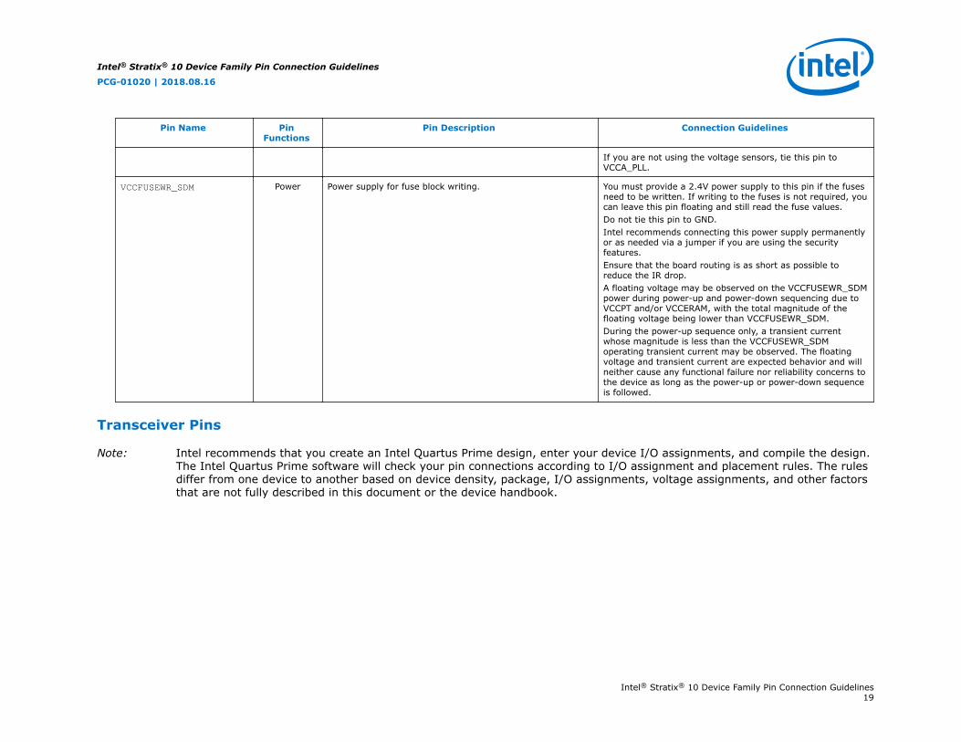
VCCFUSEWR_SDM Power Power supply for fuse block writing. You must provide a 2.4V power supply to this pin if the fusesneed to be written. If writing to the fuses is not required, youcan leave this pin floating and still read the fuse values.Do not tie this pin to GND.Intel recommends connecting this power supply permanentlyor as needed via a jumper if you are using the securityfeatures.Ensure that the board routing is as short as possible toreduce the IR drop.A floating voltage may be observed on the VCCFUSEWR_SDMpower during power-up and power-down sequencing due toVCCPT and/or VCCERAM, with the total magnitude of thefloating voltage being lower than VCCFUSEWR_SDM.During the power-up sequence only, a transient currentwhose magnitude is less than the VCCFUSEWR_SDMoperating transient current may be observed. The floatingvoltage and transient current are expected behavior and willneither cause any functional failure nor reliability concerns tothe device as long as the power-up or power-down sequenceis followed.
Transceiver Pins
Note: Intel recommends that you create an Intel Quartus Prime design, enter your device I/O assignments, and compile the design.The Intel Quartus Prime software will check your pin connections according to I/O assignment and placement rules. The rulesdiffer from one device to another based on device density, package, I/O assignments, voltage assignments, and other factorsthat are not fully described in this document or the device handbook.
Intel® Stratix® 10 Device Family Pin Connection Guidelines
PCG-01020 | 2018.08.16
Intel® Stratix® 10 Device Family Pin Connection Guidelines19

Table 12. Transceiver Pins (See Notes 4 through 10)—PreliminaryFor more information on the pin description and connection guidelines of the nPERST[L,R][0:2] pins, refer to the Optional/Dual-Purpose Configuration Pinssection.
Pin Name PinFunctions
Pin Description Connection Guidelines
VCCR_GXB[L1,R4][C,D,E,F,G,H,I,J,K,L,M,N]
Power Analog power, receiver, specific to each transceiver bank ofthe left (L) side or right (R) side of the device.
Connect VCCR_GXB pins to a 1.03V or 1.12V low noiseswitching regulator depending on the transceiver data rate.VCCR_GXB and VCCT_GXB pins on the same transceiver tileof the device must have the same voltage. This voltage isdetermined by the voltage level of the highest data rate bankon that tile.When all of the transceivers on the same H-tile or L-tile arenot used, you may power down the transceivers in those tilesby connecting its VCCR_GXB and VCCT_GXB to GND.Place a 22-nF decoupling capacitor between each VCCR_GXBpower pin and GND pin on the back side of the BGA pin field.See Notes 2, 3, 4, 7, and 10 in Notes to Intel Stratix 10 GXPin Connection Guidelines.
VCCT_GXB[L1,R4][C,D,E,F,G,H,I,J,K,L,M,N]
Power Analog power, transmitter, specific to each transceiver bankof the left (L) side or right (R) side of the device.
Connect VCCT_GXB pins to a 1.03V or 1.12V low noiseswitching regulator depending on the transceiver data rate.VCCR_GXB and VCCT_GXB pins on the same transceiver tileof the device must have the same voltage. This voltage isdetermined by the voltage level of the highest data rate bankon that tile.When all of the transceivers on the same H-tile or L-tile arenot used, you may power down the transceivers in those tilesby connecting its VCCR_GXB and VCCT_GXB to GND.Place a 22-nF decoupling capacitor between each VCCT_GXBpower pin and GND pin on the back side of the BGA pin field.See Notes 2, 3, 4, 7, and 10 in Notes to Intel Stratix 10 GXPin Connection Guidelines.
VCCH_GXB[L1,R4][C,D,E,F,G,H,I,J,K,L,M,N]
Power Analog power, block level transmitter buffers, specific to theleft (L) side or right (R) side of the device.
Connect VCCH_GXB to 1.8V low noise switching regulator.With a proper isolation filtering, you have the option tosource VCCH_GXB from the same regulator as VCCPT.To minimize the regulator switching noise impact on channeljitter performance, keep the switching frequency forVCCH_GXB regulator below 2 MHz. For OTN applications, theswitching frequency for VCCH_GXB is recommended to bebelow 500 KHz.Place a 22-nF decoupling capacitor between each VCCH_GXBpower pin and GND pin on the back side of the BGA pin field.
continued...
Intel® Stratix® 10 Device Family Pin Connection Guidelines
PCG-01020 | 2018.08.16
Intel® Stratix® 10 Device Family Pin Connection Guidelines20

Pin Name PinFunctions
Pin Description Connection Guidelines
A leakage voltage may be observed on the VCCH_GXB powerrail before the VCCH_GXB is powered on due to leakageinside the device during the power-up and power-downsequencing. The total magnitude of this leakage voltage islower than VCCH_GXB and this is an expected behavior.During the power-up sequence only, a transient currentwhose magnitude is less than the VCCH_GXB static operatingcurrent may be observed. The floating voltage and transientcurrent are expected behavior and will neither cause anyfunctional failure nor reliability concerns to the device as longas the power-up or power-down sequence is followed.See Notes 2, 3, 4, 7, and 10 in Notes to Intel Stratix 10 GXPin Connection Guidelines.
GXB[L1,R4][C,D,E,F,G,H,I,J,K,L,M,N]_RX_CH[0:5]p
GXB[L1,R4][C,D,E,F,G,H,I,J,K,L,M,N]_REFCLK[0:5]p
Input High speed positive differential receiver channels or REFCLKinputs. Specific to each transceiver bank of the left (L) side orright (R) side of the device.
These pins can be AC-coupled or DC-coupled when used. Formore information, refer to the Intel Stratix 10 DeviceDatasheet.Connect all unused GXB_RXp pins directly to GND.
GXB[L1,R4][C,D,E,F,G,H,I,J,K,L,M,N]_RX_CH[0:5]n
GXB[L1,R4][C,D,E,F,G,H,I,J,K,L,M,N]_REFCLK[0:5]n
Input High speed negative differential receiver channels or REFCLKinputs. Specific to each transceiver bank of the left (L) side orright (R) side of the device.
These pins can be AC-coupled or DC-coupled when used. Formore information, refer to the Intel Stratix 10 DeviceDatasheet.Connect all unused GXB_RXn pins directly to GND.
GXB[L1,R4][C,D,E,F,G,H,I,J,K,L,M,N]_TX_CH[0:5]p
Output High speed positive differential transmitter channels. Specificto each transceiver bank of the left (L) side or right (R) sideof the device.
Leave all unused GXB_TXp pins floating.
GXB[L1,R4][C,D,E,F,G,H,I,J,K,L,M,N]_TX_CH[0:5]n
Output High speed negative differential transmitter channels.Specific to each transceiver bank of the left (L) side or right(R) side of the device.
Leave all unused GXB_TXn pins floating.
REFCLK_GXB[L1,R4][C,D,E,F,G,H,I,J,K,L,M,N]_CH[B,T]p
Input High speed differential reference clock positive receiverchannels, specific to each transceiver bank of the left (L) sideor right (R) side of the device.REFCLK_GXB can be used as dedicated clock input pins withfPLL for core clock generation even when the transceiverchannel is not used.
These pins should be AC-coupled or DC-coupled when used.For HCSL I/O standard, it only supports DC coupling. In thePCI Express configuration, DC-coupling is allowed on theREFCLK if the selected REFCLK I/O standard is HCSL.Connect all unused pins individually to GND.
continued...
Intel® Stratix® 10 Device Family Pin Connection Guidelines
PCG-01020 | 2018.08.16
Intel® Stratix® 10 Device Family Pin Connection Guidelines21

Pin Name PinFunctions
Pin Description Connection Guidelines
See Note 9 in Notes to Intel Stratix 10 GX Pin ConnectionGuidelines.
REFCLK_GXB[L1,R4][C,D,E,F,G,H,I,J,K,L,M,N]_CH[B,T]n
Input High speed differential reference clock complement,complementary receiver channel, specific to each transceiverbank of the left (L) side or right (R) side of the device.REFCLK_GXB can be used as dedicated clock input pins withfPLL for core clock generation even when the transceiverchannel is not used.
These pins should be AC-coupled or DC-coupled when used.For HCSL I/O standard, it only supports DC coupling. In thePCI Express configuration, DC-coupling is allowed on theREFCLK if the selected REFCLK I/O standard is HCSL.Connect all unused pins individually to GND.See Note 9 in Notes to Intel Stratix 10 GX Pin ConnectionGuidelines.
RREF_[T,M,B][L,R] Input Reference resistor for fPLL, IOPLL, and transceiver, specific tothe top (T), middle (M), and bottom (B) of the left (L) side orright (R) side of the device.
If any REFCLK pin or transceiver channel on one side (left orright) of the device, IOPLL, or fPLL is used, you must connecteach RREF pin on that side of the device to its own individual2kΩ +/-1% resistor to GND.Otherwise, you can connect each RREF pin on that side of thedevice directly to GND. In the PCB layout, the trace from thispin to the resistor needs to be routed so that it avoids anyaggressor signals.
Secure Device Manager (SDM) Pins
Note: Intel recommends that you create an Intel Quartus Prime design, enter your device I/O assignments, and compile the design.The software will check your pin connections according to I/O assignment and placement rules. The rules differ from onedevice to another based on device density, package, I/O assignments, voltage assignments, and other factors that are notfully described in this document or the device handbook.
Table 13. SDM Pins (See Notes 11 and 12)—Preliminary
Pin Name PinFunctions
Pin Description Connection Guidelines
RREF_SDM Input Reference resistor input for the PLLs of the SDM interface. Connect a 2kΩ +/-1% resistor to GND.
SDM_IO0 PWRMGT_SCL
PMBus Power Management Clock.By default, the PWRMGT_SCL function is enabled inSDM_IO14. If you use Avalon-ST x8 configuration scheme,you must implement this function using the SDM_IO0 pin.This pin is pulled low internally by a 25-kΩ resistor when thedevice is powered up.
This pin is used as the clock pin for the PMBus interface.When a –V device is used, you must enable the SmartVIDconnection between the device and the VCC voltage regulatorto allow the FPGA to directly control its core voltagerequirements. You can do this by connecting thePWRMGT_SCL and PWRMGT_SDA signals to the VCC voltage
continued...
Intel® Stratix® 10 Device Family Pin Connection Guidelines
PCG-01020 | 2018.08.16
Intel® Stratix® 10 Device Family Pin Connection Guidelines22

Pin Name PinFunctions
Pin Description Connection Guidelines
When this pin is used as the PWRMGT_SCL function, this pinrequires a pull-up resistor to the 1.8V VCCIO_SDM supply.Intel recommends a pull-up value of 5.1-kΩ to 10-kΩdepending on the loading of this pin. Use the voltage leveltranslators when interfacing to the PMBus interfaces requiringvoltages other than 1.8V.
regulator for the PMBus master mode and the PWRMGT_SCL,PWRMGT_SDA, and PWRMGT_ALERT signals to the VCCvoltage regulator for the PMBus slave mode.Connect this pin to the PMBus clock pin of your regulator.
PWRMGT_PWM0
PWM_PWM0.This pin is pulled low internally by a 25-kΩ resistor when thedevice is powered up.
This signal is used for the pulse width modulation (PWM)interface between the Intel Stratix 10 device and the voltageregulator for the SmartVID feature.When a –V device is used, you must enable the SmartVIDconnection between the device and the VCC voltage regulatorto allow the FPGA to directly control its core voltagerequirements. Intel recommends using the PMBus interface.The PWM interface may be supported in the future IntelQuartus Prime release.
INIT_DONE The INIT_DONE pin indicates the device has enter user modeupon completion of configuration. SDM_IO0 is therecommended pin to implement the INIT_DONE function ifthis function is enabled in the Intel Quartus Prime software.Intel recommends you to use this pin as it has an internalweak pull-down for the correct function during power up.The INIT_DONE function can also be implemented usingother unused SDM I/O pins.This pin is pulled low internally by a 25-kΩ resistor when thedevice is powered up.
When the INIT_DONE function is enabled, this pin will drivehigh when configuration is completed and the device goesinto user mode.
PWRMGT_ALERT
PMBus Power Management Alert.When this pin is used as the PWRMGT_ALERT function, thispin requires a pull-up resistor to the 1.8V VCCIO_SDMsupply. Intel recommends a pull-up value of 5.1-kΩ to 10-kΩdepending on the loading of this pin. Use the voltage leveltranslators when interfacing to the PMBus interfaces requiringvoltages other than 1.8V.This pin is pulled high internally by a 25-kΩ resistor when thedevice is powered up.
This pin is used as the ALERT function for the PMBus interfacewhen the Intel Stratix 10 –V is the PMBus slave.When using the SmartVID feature with the Intel Stratix 10 –Vdevice as a PMBus slave, you must connect either theSDM_IO0 or SDM_IO12 pin as the PWRMGT_ALERT signalalong with the PWRMGT_SCL and PWRMGT_SDA signals tothe PMBus master device to complete the SmartVID powermanagement interface. The PMBus master device reads theVID codes from the Intel Stratix 10 slave and programs thevoltage regulator to output the correct VID voltage.Connect this pin to the PMBus ALERT pin of your regulator.
HPS_COLD_nRESET
This is an active low, bidirectional pin. By default, this pinacts as an input pin to the SDM. When asserted externally forat least 5ms, this pin will generate interrupt to the SDM. TheSDM will then initiate a cold reset procedure to the HPS and
Connect this pin through a 1–10-kΩ pull up to theVCCIO_SDM supply.
continued...
Intel® Stratix® 10 Device Family Pin Connection Guidelines
PCG-01020 | 2018.08.16
Intel® Stratix® 10 Device Family Pin Connection Guidelines23

Pin Name PinFunctions
Pin Description Connection Guidelines
its peripherals. If the cold reset is generated from internalsources (for example, the HPS EL3 software), the SDM willswitch this pin to output and drive a pulse to indicate reset.Once the cold reset procedure is complete, this pin will beswitched back to input. There is an internal 25-kΩ pull up onthis pin.
SDM_IO1 AVSTx8_DATA2
Avalon-ST Interface Data 2.This pin is pulled high internally by a 25-kΩ resistor when thedevice is powered up.
Connect this pin to the data2 pin of an external configurationcontroller when configuring using the Avalon-ST x8 interface.
AS_DATA1 Active Serial Data 1.This pin is pulled high internally by a 25-kΩ resistor when thedevice is powered up.
Connect this pin to the data1 pin of the EPCQ-L device whenconfiguring from the EPCQ-L device.
SDMMC_CFG_DATA1
SD/MMC Card Data 1.This pin is pulled high internally by a 25-kΩ resistor when thedevice is powered up.
Connect this pin to the data1 pin of the SD/MMC card flashdevice when configuring from the SD/MMC flash.
SDM_IO2 AVSTx8_DATA0
Avalon Stream Interface Data 0.This pin is pulled high internally by a 25-kΩ resistor when thedevice is powered up.
Connect this pin to the data0 pin of an external configurationcontroller when configuring using the Avalon-ST x8 interface.
AS_CLK Active Serial Clock.This pin is pulled high internally by a 25-kΩ resistor when thedevice is powered up.
Connect this pin to the clock input of the EPCQ-L device whenconfiguring from the EPCQ-L device.
SDMMC_CFG_DATA0
SD/MMC Card Data 0.This pin is pulled high internally by a 25-kΩ resistor when thedevice is powered up.
Connect this pin to the data0 pin of the SD/MMC card flashdevice when configuring from the SD/MMC flash.
SDM_IO3 AVSTx8_DATA3
Avalon Stream Interface Data 3.This pin is pulled high internally by a 25-kΩ resistor when thedevice is powered up.
Connect this pin to the data3 pin of an external configurationcontroller when configuring using the Avalon-ST x8 interface.
AS_DATA2 Active Serial Data 2.This pin is pulled high internally by a 25-kΩ resistor when thedevice is powered up.
Connect this pin to the data2 pin of the EPCQ-L device whenconfiguring from the EPCQ-L device.
SDMMC_CFG_DATA2
SD/MMC Card Data 2.This pin is pulled high internally by a 25-kΩ resistor when thedevice is powered up.
Connect this pin to the data2 pin of the SD/MMC card flashdevice when configuring from the SD/MMC flash.
continued...
Intel® Stratix® 10 Device Family Pin Connection Guidelines
PCG-01020 | 2018.08.16
Intel® Stratix® 10 Device Family Pin Connection Guidelines24

Pin Name PinFunctions
Pin Description Connection Guidelines
SDM_IO4 AVSTx8_DATA1
Avalon Stream Interface Data 1.This pin is pulled high internally by a 25-kΩ resistor when thedevice is powered up.
Connect this pin to the data1 pin of an external configurationcontroller when configuring using the Avalon-ST x8 interface.
AS_DATA0 Active Serial Data 0.This pin is pulled high internally by a 25-kΩ resistor when thedevice is powered up.
Connect this pin to the data0 pin of the EPCQ-L device whenconfiguring from the EPCQ-L device.
SDMMC_CFG_CMD
SD/MMC Card Command.This pin is pulled high internally by a 25-kΩ resistor when thedevice is powered up.
Connect this pin to the command input of the SD/MMC cardflash device when configuring from the SD/MMC flash.
SDM_IO5 MSEL[0] Configuration input pins that set the configuration scheme forthe FPGA device.This pin is pulled high internally by a 25-kΩ resistor when thedevice is powered up.
This pin will function as MSEL[0] during power up and resetto determine the configuration scheme. This pin needs to bepulled-up to VCCIO_SDM or pulled-down to GND through a4.7-kΩ resistor depending on your configuration scheme.Once the pin completes the MSEL function, it will thenfunction according to the configuration scheme you haveselected.For more information, refer to the Intel Stratix 10Configuration User Guide.
CONF_DONE The CONF_DONE pin indicates all configuration data has beenreceived. By default, SDM_IO16 is the recommended pin toimplement the CONF_DONE function. If you are using theAvalon-ST x8 configuration scheme and PMBus powermanagement feature, the PWRMGT_SDA function can beassigned to either SDM_IO12 or SDM_IO16. Use SDM_IO5 toimplement the CONF_DONE function if SDM_IO16 is used forthe PWRMGT_SDA function.This pin is pulled high internally by a 25-kΩ resistor when thedevice is powered up.
Connect the CONF_DONE pin to the external configurationcontroller when configuring using the Avalon-ST interface.
AS_nCSO0 Active Serial Chip Select 0.This pin is pulled high internally by a 25-kΩ resistor when thedevice is powered up.
Connect this pin to the nCS input of the first EPCQ-L devicewhen configuring from EPCQ-L devices.
SDMMC_CFG_CCLK
SD/MMC Card Clock.This pin is pulled high internally by a 25-kΩ resistor when thedevice is powered up.
Connect this pin to the clock input of the SD/MMC card flashdevice when configuring from the SD/MMC flash.
INIT_DONE The INIT_DONE pin indicates the device has enter user modeupon completion of configuration. SDM_IO is therecommended pin to implement the INIT_DONE function if
When the INIT_DONE function is enabled, this pin will drivehigh when configuration is completed and the device goesinto user mode.
continued...
Intel® Stratix® 10 Device Family Pin Connection Guidelines
PCG-01020 | 2018.08.16
Intel® Stratix® 10 Device Family Pin Connection Guidelines25

Pin Name PinFunctions
Pin Description Connection Guidelines
this function is enabled in the Intel Quartus Prime software.If you use AVST x8 or AVST x32 configuration scheme, youcan use this pin as it has a 4.7-kΩ pull-down on the MSEL[0]pin for the correct function during power up.The INIT_DONE function can also be implemented usingother unused SDM I/O pins.
SDM_IO6 AVSTx8_DATA4
Avalon Stream Interface Data 4.This pin is pulled high internally by a 25-kΩ resistor when thedevice is powered up.
Connect this pin to the data4 pin of an external configurationcontroller when configuring using the Avalon-ST x8 interface.
AS_DATA3 Active Serial Data 3.This pin is pulled high internally by a 25-kΩ resistor when thedevice is powered up.
Connect this pin to the data3 pin of the EPCQ-L device whenconfiguring from the EPCQ-L device.
SDMMC_CFG_DATA3
SD/MMC Card Data 3.This pin is pulled high internally by a 25-kΩ resistor when thedevice is powered up.
Connect this pin to the data3 pin of the SD/MMC card flashdevice when configuring from the SD/MMC flash.
SDM_IO7 MSEL[1] Configuration input pins that set the configuration scheme forthe FPGA device.This pin is pulled high internally by a 25-kΩ resistor when thedevice is powered up.
This pin will function as MSEL[1] during power up and resetto determine the configuration scheme. This pin needs to bepulled-up to VCCIO_SDM or pulled-down to GND through a4.7-kΩ resistor depending on your configuration scheme.Once the pin completes the MSEL function, it will thenfunction according to the configuration scheme you haveselected.For more information, refer to the Intel Stratix 10Configuration User Guide.
AS_nCSO2 Active Serial Chip Select 2.This pin is pulled high internally by a 25-kΩ resistor when thedevice is powered up.
Connect this pin to the nCS input of the third EPCQ-L devicewhen configuring from EPCQ-L devices.
SDM_IO8 AVST_READY Avalon Stream Interface Data Ready.This pin is pulled low internally by a 25-kΩ resistor when thedevice is powered up.
Connect this pin to the ready signal output of the externalconfiguration controller when configuring using the Avalon-STx8 , x16, or x32 interface.
AS_nCSO3 Active Serial Chip Select 3.This pin is pulled low internally by a 25-kΩ resistor when thedevice is powered up.
Connect this pin to the nCS input of the fourth EPCQ-L devicewhen configuring from EPCQ-L devices.
SDMMC_CFG_DATA4
SD/MMC Card Data 4.This pin is pulled low internally by a 25-kΩ resistor when thedevice is powered up.
Connect this pin to the data4 pin of the SD/MMC card flashdevice when configuring from the SD/MMC flash.
continued...
Intel® Stratix® 10 Device Family Pin Connection Guidelines
PCG-01020 | 2018.08.16
Intel® Stratix® 10 Device Family Pin Connection Guidelines26

Pin Name PinFunctions
Pin Description Connection Guidelines
SDM_IO9 MSEL[2] Configuration input pins that set the configuration scheme forthe FPGA device.This pin is pulled high internally by a 25-kΩ resistor when thedevice is powered up.
This pin will function as MSEL[2] during power up and resetto determine the configuration scheme. This pin needs to bepulled-up to VCCIO_SDM or pulled-down to GND through a4.7-kΩ resistor depending on your configuration scheme.Once the pin completes the MSEL function, it will thenfunction according to the configuration scheme you haveselected.For more information, refer to the Intel Stratix 10Configuration User Guide.
AS_nCSO1 Active Serial Chip Select 1.This pin is pulled high internally by a 25-kΩ resistor when thedevice is powered up.
Connect this pin to the nCS input of the second EPCQ-Ldevice when configuring from EPCQ-L devices.
SDM_IO10 AVSTx8_DATA7
Avalon Stream Interface Data 7.This pin is pulled high internally by a 25-kΩ resistor when thedevice is powered up.
Connect this pin to the data7 pin of an external configurationcontroller when configuring using the Avalon-ST x8 interface.
SDMMC_CFG_DATA7
SD/MMC Card Data 7.This pin is pulled high internally by a 25-kΩ resistor when thedevice is powered up.
Connect this pin to the data7 pin of the SD/MMC card flashdevice when configuring from the SD/MMC flash.
HPS_COLD_nRESET
This is an active low, bidirectional pin. By default, this pinacts as an input pin to the SDM. When asserted externally forat least 5ms, this pin will generate interrupt to the SDM. TheSDM will then initiate a cold reset procedure to the HPS andits peripherals. If the cold reset is generated from internalsources (for example, the HPS EL3 software), the SDM willswitch this pin to output and drive a pulse to indicate reset.Once the cold reset procedure is complete, this pin will beswitched back to input. There is an internal 25-kΩ pull up onthis pin.
Connect this pin through a 1–10-kΩ pull up to theVCCIO_SDM supply.
SDM_IO11 AVSTx8_VALID
Avalon Stream Interface Data Valid.This pin is pulled high internally by a 25-kΩ resistor when thedevice is powered up.
Connect this pin to the data valid pin of an externalconfiguration controller when configuring using the Avalon-STx8 interface.
PWRMGT_SDA
PMBus Power Management Serial Data.By default, use the SDM_IO11 pin for the PWRMGT_SDAfunction. If you use Avalon-ST x8 configuration scheme, youmust implement this function using the SDM_IO12 pin.When this pin is used as the PWRMGT_SDA function, this pinrequires a pull-up resistor to the 1.8V VCCIO_SDM supply.Intel recommends a pull-up value of 5.1-kΩ to 10-kΩ
This pin is used as the data pin for the PMBus interface.When a –V device is used, you must enable the SmartVIDconnection between the device and the VCC voltage regulatorto allow the FPGA to directly control its core voltagerequirements. You can do this by connecting thePWRMGT_SCL and PWRMGT_SDA signals to the VCC voltage
continued...
Intel® Stratix® 10 Device Family Pin Connection Guidelines
PCG-01020 | 2018.08.16
Intel® Stratix® 10 Device Family Pin Connection Guidelines27

Pin Name PinFunctions
Pin Description Connection Guidelines
depending on the loading of this pin. Use the voltage leveltranslators when interfacing to the PMBus interfaces requiringvoltages other than 1.8V.This pin is pulled high internally by a 25-kΩ resistor when thedevice is powered up.
regulator for the PMBus master mode and the PWRMGT_SCL,PWRMGT_SDA, and PWRMGT_ALERT signals to the VCCvoltage regulator for the PMBus slave mode.Connect this pin to the PMBus data pin of your regulator.
HPS_COLD_nRESET
This is an active low, bidirectional pin. By default, this pinacts as an input pin to the SDM. When asserted externally forat least 5ms, this pin will generate interrupt to the SDM. TheSDM will then initiate a cold reset procedure to the HPS andits peripherals. If the cold reset is generated from internalsources (for example, the HPS EL3 software), the SDM willswitch this pin to output and drive a pulse to indicate reset.Once the cold reset procedure is complete, this pin will beswitched back to input. There is an internal 25-kΩ pull up onthis pin.
Connect this pin through a 1–10-kΩ pull up to theVCCIO_SDM supply.
SDM_IO12 PWRMGT_PWM0
PWM_PWM0.This pin is pulled high internally by a 25-kΩ resistor when thedevice is powered up.
This signal is used for the pulse width modulation (PWM)interface between the Intel Stratix 10 device and the voltageregulator for the SmartVID feature.When a –V device is used, you must enable the SmartVIDconnection between the device and the VCC voltage regulatorto allow the FPGA to directly control its core voltagerequirements. Intel recommends using the PMBus interface.The PWM interface may be supported in the future IntelQuartus Prime release.
PWRMGT_SDA
PMBus Power Management Serial Data.By default, use the SDM_IO11 pin for the PWRMGT_SDAfunction. If you use Avalon-ST x8 configuration scheme, youmust implement this function using the SDM_IO12 orSDM_IO16 pin.When this pin is used as the PWRMGT_SDA function, this pinrequires a pull-up resistor to the 1.8V VCCIO_SDM supply.Intel recommends a pull-up value of 5.1-kΩ to 10-kΩdepending on the loading of this pin. Use the voltage leveltranslators when interfacing to the PMBus interfaces requiringvoltages other than 1.8V.This pin is pulled high internally by a 25-kΩ resistor when thedevice is powered up.
This pin is used as the data pin for the PMBus.When a –V device is used, you must enable the SmartVIDconnection between the device and the VCC voltage regulatorto allow the FPGA to directly control its core voltagerequirements. You can do this by connecting thePWRMGT_SCL and PWRMGT_SDA signals to the VCC voltageregulator for the PMBus master mode and the PWRMGT_SCL,PWRMGT_SDA, and PWRMGT_ALERT signals to the VCCvoltage regulator for the PMBus slave mode.Connect this pin to the PMBus data pin of your regulator.
PWRMGT_ALERT
PMBus Power Management Alert. This pin is used as the ALERT function for the PMBus interfacewhen the Intel Stratix 10 –V is the PMBus slave.
continued...
Intel® Stratix® 10 Device Family Pin Connection Guidelines
PCG-01020 | 2018.08.16
Intel® Stratix® 10 Device Family Pin Connection Guidelines28

Pin Name PinFunctions
Pin Description Connection Guidelines
When this pin is used as the PWRMGT_ALERT function, thispin requires a pull-up resistor to the 1.8V VCCIO_SDMsupply. Intel recommends a pull-up value of 5.1-kΩ to 10-kΩdepending on the loading of this pin. Use the voltage leveltranslators when interfacing to the PMBus interfaces requiringvoltages other than 1.8V.This pin is pulled high internally by a 25-kΩ resistor when thedevice is powered up.
When using the SmartVID feature with the Intel Stratix 10 –Vdevice as a PMBus slave, you must connect either theSDM_IO0 or SDM_IO12 pin as the PWRMGT_ALERT signalalong with the PWRMGT_SCL and PWRMGT_SDA signals tothe PMBus master device to complete the SmartVID powermanagement interface. The PMBus master device reads theVID codes from the Intel Stratix 10 slave and programs thevoltage regulator to output the correct VID voltage.Connect this pin to the PMBus ALERT pin of your regulator.
HPS_COLD_nRESET
This is an active low, bidirectional pin. By default, this pinacts as an input pin to the SDM. When asserted externally forat least 5ms, this pin will generate interrupt to the SDM. TheSDM will then initiate a cold reset procedure to the HPS andits peripherals. If the cold reset is generated from internalsources (for example, the HPS EL3 software), the SDM willswitch this pin to output and drive a pulse to indicate reset.Once the cold reset procedure is complete, this pin will beswitched back to input. There is an internal 25-kΩ pull up onthis pin.
Connect this pin through a 1–10-kΩ pull up to theVCCIO_SDM supply.
SDM_IO13 AVSTx8_DATA5
Avalon Stream Interface Data 5.This pin is pulled high internally by a 25-kΩ resistor when thedevice is powered up.
This pin has multiple functions depending on theconfiguration mode used:• Connect this pin to the data5 pin of an external
configuration controller when configuring using theAvalon-ST x8 interface.
• Connect this pin to the data5 pin of the SD/MMC cardflash device when configuring from the SD/MMC flash.
SDMMC_CFG_DATA5
SD/MMC Card Data 5.This pin is pulled high internally by a 25-kΩ resistor when thedevice is powered up.
HPS_COLD_nRESET
This is an active low, bidirectional pin. By default, this pinacts as an input pin to the SDM. When asserted externally forat least 5ms, this pin will generate interrupt to the SDM. TheSDM will then initiate a cold reset procedure to the HPS andits peripherals. If the cold reset is generated from internalsources (for example, the HPS EL3 software), the SDM willswitch this pin to output and drive a pulse to indicate reset.Once the cold reset procedure is complete, this pin will beswitched back to input. There is an internal 25-kΩ pull up onthis pin.
Connect this pin through a 1–10-kΩ pull up to theVCCIO_SDM supply.
SDM_IO14 AVSTx8_CLK Avalon Stream Interface Clock Input.This pin is pulled high internally by a 25-kΩ resistor when thedevice is powered up.
Connect this pin to the clock output of an externalconfiguration controller when configuring using the Avalon-STx8 interface.
continued...
Intel® Stratix® 10 Device Family Pin Connection Guidelines
PCG-01020 | 2018.08.16
Intel® Stratix® 10 Device Family Pin Connection Guidelines29

Pin Name PinFunctions
Pin Description Connection Guidelines
PWRMGT_SCL
PMBus Power Management Clock.By default, the PWRMGT_SCL function is enabled inSDM_IO14. If you use Avalon-ST x8 configuration scheme,you must implement this function using the SDM_IO0 pin.When this pin is used as the PWRMGT_SCL function, this pinrequires a pull-up resistor to the 1.8V VCCIO_SDM supply.Intel recommends a pull-up value of 5.1-kΩ to 10-kΩdepending on the loading of this pin. Use the voltage leveltranslators when interfacing to the PMBus interfaces requiringvoltages other than 1.8V.This pin is pulled high internally by a 25-kΩ resistor when thedevice is powered up.
This pin is used as the clock pin for the PMBus interface.When a –V device is used, you must enable the SmartVIDconnection between the device and the VCC voltage regulatorto allow the FPGA to directly control its core voltagerequirements. You can do this by connecting thePWRMGT_SCL and PWRMGT_SDA signals to the VCC voltageregulator for the PMBus master mode and the PWRMGT_SCL,PWRMGT_SDA, and PWRMGT_ALERT signals to the VCCvoltage regulator for the PMBus slave mode.Connect this pin to the PMBus clock pin of your regulator.
HPS_COLD_nRESET
This is an active low, bidirectional pin. By default, this pinacts as an input pin to the SDM. When asserted externally forat least 5ms, this pin will generate interrupt to the SDM. TheSDM will then initiate a cold reset procedure to the HPS andits peripherals. If the cold reset is generated from internalsources (for example, the HPS EL3 software), the SDM willswitch this pin to output and drive a pulse to indicate reset.Once the cold reset procedure is complete, this pin will beswitched back to input. There is an internal 25-kΩ pull up onthis pin.
Connect this pin through a 1–10-kΩ pull up to theVCCIO_SDM supply.
SDM_IO15 AVSTx8_DATA6
Avalon Stream Interface Data 6.This pin is pulled high internally by a 25-kΩ resistor when thedevice is powered up.
Connect this pin to the data6 pin of an external configurationcontroller when configuring using the Avalon-ST x8 interface.
SDMMC_CFG_DATA6
SD/MMC Card Data 6.This pin is pulled high internally by a 25-kΩ resistor when thedevice is powered up.
Connect this pin to the data6 pin of the SD/MMC card flashdevice when configuring from the SD/MMC flash.
HPS_COLD_nRESET
This is an active low, bidirectional pin. By default, this pinacts as an input pin to the SDM. When asserted externally forat least 5ms, this pin will generate interrupt to the SDM. TheSDM will then initiate a cold reset procedure to the HPS andits peripherals. If the cold reset is generated from internalsources (for example, the HPS EL3 software), the SDM willswitch this pin to output and drive a pulse to indicate reset.Once the cold reset procedure is complete, this pin will beswitched back to input. There is an internal 25-kΩ pull up onthis pin.
Connect this pin through a 1–10-kΩ pull up to theVCCIO_SDM supply.
continued...
Intel® Stratix® 10 Device Family Pin Connection Guidelines
PCG-01020 | 2018.08.16
Intel® Stratix® 10 Device Family Pin Connection Guidelines30

Pin Name PinFunctions
Pin Description Connection Guidelines
SDM_IO16 CONF_DONE The CONF_DONE pin indicates device configuration hascompleted. SDM_IO16 is the recommended pin to implementthe CONF_DONE function, if this pin is enabled in the IntelQuartus Prime software.Intel recommends you to use this pin as it has a weak pull-down for the correct function during power up. If you areusing the Avalon-ST x8 configuration scheme and PMBuspower management feature, the PWRMGT_SDA function canbe assigned to either SDM_IO12 or SDM_IO16. Use SDM_IO5to implement the CONF_DONE function if SDM_IO16 is usedfor the PWRMGT_SDA function.The CONF_DONE function can also be implemented usingother unused SDM I/O pins.This pin is pulled low internally by a 25-kΩ resistor when thedevice is powered up.
Connect the CONF_DONE pin to the external configurationcontroller when configuring using the Avalon-ST interface.
PWRMGT_SDA
PMBus Power Management Serial Data.By default, use the SDM_IO11 pin for the PWRMGT_SDAfunction.When this pin is used as the PWRMGT_SDA function, this pinrequires a pull-up resistor to the 1.8V VCCIO_SDM supply.Intel recommends a pull-up value of 5.1-kΩ to 10-kΩdepending on the loading of this pin. Use the voltage leveltranslators when interfacing to the PMBus interfaces requiringvoltages other than 1.8V.This pin is pulled low internally by a 25-kΩ resistor when thedevice is powered up.
This pin is used as the data pin for the PMBus interface.When a –V device is used, you must enable the SmartVIDconnection between the device and the VCC voltage regulatorto allow the FPGA to directly control its core voltagerequirements. You can do this by connecting thePWRMGT_SCL and PWRMGT_SDA signals to the VCC voltageregulator for the PMBus master mode and the PWRMGT_SCL,PWRMGT_SDA, and PWRMGT_ALERT signals to the VCCvoltage regulator for the PMBus slave mode.Connect this pin to the PMBus data pin of your regulator.
INIT_DONE The INIT_DONE pin indicates the device has enter user modeupon completion of configuration. SDM_IO0 is therecommended pin to implement the INIT_DONE function ifthis function is enabled in the Intel Quartus Prime software.Intel recommends you to use this pin as it has an internalweak pull-down for the correct function during power up.The INIT_DONE function can also be implemented usingother unused SDM I/O pins.This pin is pulled low internally by a 25-kΩ resistor when thedevice is powered up.
When the INIT_DONE function is enabled, this pin will drivehigh when configuration is completed and the device goesinto user mode.
HPS_COLD_nRESET
This is an active low, bidirectional pin. By default, this pinacts as an input pin to the SDM. When asserted externally forat least 5ms, this pin will generate interrupt to the SDM. TheSDM will then initiate a cold reset procedure to the HPS andits peripherals. If the cold reset is generated from internalsources (for example, the HPS EL3 software), the SDM willswitch this pin to output and drive a pulse to indicate reset.Once the cold reset procedure is complete, this pin will beswitched back to input. There is an internal 25-kΩ pull up onthis pin.
Connect this pin through a 1–10-kΩ pull up to theVCCIO_SDM supply.
Intel® Stratix® 10 Device Family Pin Connection Guidelines
PCG-01020 | 2018.08.16
Intel® Stratix® 10 Device Family Pin Connection Guidelines31

Notes to Intel Stratix 10 GX Pin Connection Guidelines
Note: Intel recommends that you create an Intel Quartus Prime design, enter your device I/O assignments, and compile the design.The Intel Quartus Prime software will check your pin connections according to I/O assignment and placement rules. The rulesdiffer from one device to another based on device density, package, I/O assignments, voltage assignments, and other factorsthat are not fully described in this document or the device handbook.
Intel provides these guidelines only as recommendations. It is the responsibility of the designer to apply simulation results tothe design to verify proper device functionality.
1. These pin connection guidelines are created based on the Intel Stratix 10 GX device variant.
2. Select the capacitance values for the power supply after you consider the amount of power they need to supply over thefrequency of operation of the particular circuit being decoupled. Calculate the target impedance for the power plane basedon current draw and voltage drop requirements of the device/supply. Then, decouple the power plane using theappropriate number of capacitors. On-board capacitors do not decouple higher than 100 MHz due to “Equivalent SeriesInductance” of the mounting of the packages. Consider proper board design techniques such as interplane capacitancewith low inductance for higher frequency decoupling. Refer to the PDN tool.
3. Use the Intel Stratix 10 Early Power Estimator (EPE) to determine the preliminary current requirements for VCC and otherpower supplies. Use the Intel Quartus Prime Power Analyzer for the most accurate current requirements for this and otherpower supplies.
4. These supplies may share power planes across multiple Intel Stratix 10 devices.
5. Power pins should not share breakout vias from the BGA. Each ball on the BGA needs to have its own dedicated breakoutvia. VCC must not share breakout vias.
6. Example 1 and Example 2 illustrate the power supply sharing guidelines for the Intel Stratix 10 GX devices.
7. Low Noise Switching Regulator - defined as a switching regulator circuit encapsulated in a thin surface mount packagecontaining the switch controller, power FETs, inductor, and other support components. The switching frequency is usuallybetween 800kHz and 1MHz and has fast transient response. The switching frequency range is not an Intel requirement.
8. The number of modular I/O banks on Intel Stratix 10 devices depends on the device density. For the indexes available fora specific device, please refer to the I/O Bank section in the Intel Stratix 10 General Purpose I/O User Guide.
9. For AC-coupled links, the AC-coupling capacitor can be placed anywhere along the channel. PCI Express protocol requiresthe AC-coupling capacitor to be placed on the transmitter side of the interface that permits adapters to be plugged andunplugged.
10. Decoupling for these pins depends on the design decoupling requirements of the specific board.
Intel® Stratix® 10 Device Family Pin Connection Guidelines
PCG-01020 | 2018.08.16
Intel® Stratix® 10 Device Family Pin Connection Guidelines32

11. There are no dedicated PR_REQUEST, PR_ERROR, and PR_DONE pins. If required, you can use user I/O pins for thesefunctions.
12. There are no dedicated SEU_ERROR, or CvP_CONFDONE pins in Intel Stratix 10 devices. If required, you can use thefollowing pins for these functions:
• SEU_ERROR—SDM_IO0 or SDM_IO[10..16]
• CvP_CONFDONE—SDM_IO0 or SDM_IO[10..16]
When any of those pins are used for the SEU_ERROR function, connect those pins to an external 10-kΩ pull-up resistor tothe VCCIO_SDM supply. The CvP_CONFDONE pin does not require a pull-up resistor.
13. The device orientation is die view (bottom of chip view).
Intel Stratix 10 MX Pin Connection Guidelines
UIB and eSRAM Pins
Note: Intel recommends that you create an Intel Quartus Prime design, enter your device I/O assignments, and compile the design.The Intel Quartus Prime software will check your pin connections according to I/O assignment and placement rules. The rulesdiffer from one device to another based on device density, package, I/O assignments, voltage assignments, and other factorsthat are not fully described in this document or the device handbook.
Table 14. UIB and eSRAM Pins—Preliminary
Pin Name PinFunctions
Pin Description Connection Guidelines
CLK_ESRAM_[0,1]p EmbeddedSRAM
(eSRAM)Clock Input
Dedicated positive high speed differential reference clock pinfor eSRAM PLL.
Connect this pin to the positive terminal of an LVDS clocksource within the range of 10 MHz to 325 MHz. The frequencyselected must match the available options provided in theIntel Quartus Prime HBM2 interface PLL Reference ClockFrequency selection dialog box. Only DC-coupling issupported. The peak-to-peak jitter of this clock must meet orexceed the following jitter requirements for frequencybandwidth from 10 kHz to 1/2 of the frequency chosen:• 10 ps peak-to-peak• 1.42 ps RMS at 1e-12 BER• 1.22 ps at 1e-16 BER
continued...
Intel® Stratix® 10 Device Family Pin Connection Guidelines
PCG-01020 | 2018.08.16
Intel® Stratix® 10 Device Family Pin Connection Guidelines33

Pin Name PinFunctions
Pin Description Connection Guidelines
Connect directly to GND if unused.
CLK_ESRAM_[0,1]n eSRAM ClockInput
Dedicated complement high speed differential reference clockpin for eSRAM PLL.
Connect this pin to the negative terminal of an LVDS clocksource within the range of 10 MHz to 325 MHz. The frequencyselected must match the available options provided in theIntel Quartus Prime HBM2 interface PLL Reference ClockFrequency selection dialog box. Only DC-coupling issupported. The peak-to-peak jitter of this clock must meet orexceed the following jitter requirements for frequencybandwidth from 10 kHz to 1/2 of the frequency chosen:• 10 ps peak-to-peak• 1.42 ps RMS at 1e-12 BER• 1.22 ps at 1e-16 BERConnect directly to GND if unused.
UIB_PLL_REF_CLK_[00,01]p
UIB ClockInput
Dedicated positive high speed differential reference clock pinfor UIB PLL.
Connect this pin to the positive terminal of an LVDS clocksource within the range of 10 MHz to 325 MHz. The frequencyselected must match the available options provided in theIntel Quartus Prime HBM2 interface PLL Reference ClockFrequency selection dialog box. Only DC-coupling issupported. The peak-to-peak jitter of this clock must meet orexceed the following jitter requirements for frequencybandwidth from 10 kHz to 1/2 of the frequency chosen:• 10 ps peak-to-peak• 1.42 ps RMS at 1e-12 BER• 1.22 ps at 1e-16 BERConnect directly to GND if unused.
UIB_PLL_REF_CLK_[00,01]n
UIB ClockInput
Dedicated complement high speed differential reference clockpin for UIB PLL.
Connect this pin to the negative terminal of an LVDS clocksource within the range of 10 MHz to 325 MHz. The frequencyselected must match the available options provided in theIntel Quartus Prime HBM2 interface PLL Reference ClockFrequency selection dialog box. Only DC-coupling issupported. The peak-to-peak jitter of this clock must meet orexceed the following jitter requirements for frequencybandwidth from 10 kHz to 1/2 of the frequency chosen:• 10 ps peak-to-peak• 1.42 ps RMS at 1e-12 BER• 1.22 ps at 1e-16 BER
continued...
Intel® Stratix® 10 Device Family Pin Connection Guidelines
PCG-01020 | 2018.08.16
Intel® Stratix® 10 Device Family Pin Connection Guidelines34

Pin Name PinFunctions
Pin Description Connection Guidelines
Connect directly to GND if unused.
RREF_ESRAM_[0,1] eSRAM RREFInput
Reference resistor pin for UIB PLL and eSRAM PLL, specific totop (T) and bottom (B) of device.
If any UIB PLL or eSRAM PLL on the top or bottom side of thedevice is used, the corresponding RREF pin on that side ofthe device (top or bottom) must connect to its own individual2K Ω +/-1% resistor to GND. The PCB trace between this pinand the reference resistor needs to be carefully routed toavoid any aggressor signals.
UIB_RREF_[00,01] UIB RREFInput
Reference resistor pin for UIB IO ZQ calibration. Connect each pin through an individual 240Ω +/- 1% resistorto GND. No resistor sharing between pins is allowed. Leavethis pin floating if unused.
Intel Stratix 10 MX Power Supply Pins
Note: Intel recommends that you create an Intel Quartus Prime design, enter your device I/O assignments, and compile the design.The Intel Quartus Prime software will check your pin connections according to I/O assignment and placement rules. The rulesdiffer from one device to another based on device density, package, I/O assignments, voltage assignments, and other factorsthat are not fully described in this document or the device handbook.
Table 15. Intel Stratix 10 MX Power Supply Pins—Preliminary
Pin Name PinFunctions
Pin Description Connection Guidelines
VCCM_WORD_[BL,TL] Power Power supply for the embedded HBM2 memory. Connect these pins to a 2.5V power supply.
VCCIO_UIB_[BL,TL] Power Power supply for the Universal Interface Bus between thecore and embedded HBM2 memory.
Connect these pins to a 1.2V power supply.
Notes to Intel Stratix 10 MX Pin Connection Guidelines
Note: Intel recommends that you create an Intel Quartus Prime design, enter your device I/O assignments, and compile the design.The Intel Quartus Prime software will check your pin connections according to I/O assignment and placement rules. The rulesdiffer from one device to another based on device density, package, I/O assignments, voltage assignments, and other factorsthat are not fully described in this document or the device handbook.
Intel® Stratix® 10 Device Family Pin Connection Guidelines
PCG-01020 | 2018.08.16
Intel® Stratix® 10 Device Family Pin Connection Guidelines35

Intel provides these guidelines only as recommendations. It is the responsibility of the designer to apply simulation results tothe design to verify proper device functionality.
1. These pin connection guidelines are created based on the Intel Stratix 10 MX device variant.
2. Select the capacitance values for the power supply after you consider the amount of power they need to supply over thefrequency of operation of the particular circuit being decoupled. Calculate the target impedance for the power plane basedon current draw and voltage drop requirements of the device/supply. Then, decouple the power plane using theappropriate number of capacitors. On-board capacitors do not decouple higher than 100 MHz due to “Equivalent SeriesInductance” of the mounting of the packages. Consider proper board design techniques such as interplane capacitancewith low inductance for higher frequency decoupling. Refer to the PDN tool.
3. Use the Intel Stratix 10 Early Power Estimator (EPE) to determine the preliminary current requirements for VCC and otherpower supplies. Use the Intel Quartus Prime Power Analyzer for the most accurate current requirements for this and otherpower supplies.
4. These supplies may share power planes across multiple Intel Stratix 10 devices.
5. Power pins should not share breakout vias from the BGA. Each ball on the BGA needs to have its own dedicated breakoutvia. VCC must not share breakout vias.
6. Example 7 and Example 8 illustrate the power supply sharing guidelines for the Intel Stratix 10 MX devices.
7. Low Noise Switching Regulator - defined as a switching regulator circuit encapsulated in a thin surface mount packagecontaining the switch controller, power FETs, inductor, and other support components. The switching frequency is usuallybetween 800kHz and 1MHz and has fast transient response. The switching frequency range is not an Intel requirement.
8. The number of modular I/O banks on Intel Stratix 10 devices depends on the device density. For the indexes available fora specific device, please refer to the I/O Bank section in the Intel Stratix 10 General Purpose I/O User Guide.
9. For AC-coupled links, the AC-coupling capacitor can be placed anywhere along the channel. PCI Express protocol requiresthe AC-coupling capacitor to be placed on the transmitter side of the interface that permits adapters to be plugged andunplugged.
10. Decoupling for these pins depends on the design decoupling requirements of the specific board.
Intel Stratix 10 TX Pin Connection Guidelines
Intel® Stratix® 10 Device Family Pin Connection Guidelines
PCG-01020 | 2018.08.16
Intel® Stratix® 10 Device Family Pin Connection Guidelines36

Intel Stratix 10 TX Transceiver Pins
Note: Intel recommends that you create an Intel Quartus Prime design, enter your device I/O assignments, and compile the design.The Intel Quartus Prime software will check your pin connections according to I/O assignment and placement rules. The rulesdiffer from one device to another based on device density, package, I/O assignments, voltage assignments, and other factorsthat are not fully described in this document or the device handbook.
Table 16. Intel Stratix 10 TX Transceiver Pins—Preliminary
Pin Name PinFunctions
Pin Description Connection Guidelines
VCCH_GXE(L2, L3, R1,R2, R3)
Power Analog power, block level transmitter buffers for E-tile,specific to the left (L) side or right (R) side of the device.
Connect VCCH_GXE to a 1.1V low noise switching regulator.
VCCRT_GXE(L2, L3, R1,R2, R3)
Power Analog power, used for the high-speed circuitry for the E-tileblocks, specific to the left (L) side or right (R) side of thedevice.
Connect VCCRT_GXE to a 0.9V low noise switching regulator.
VCCRTPLL_GXE(L2, L3,R1, R2, R3)
Power Analog power, used for the high-speed circuitry for the E-tileblocks, specific to the left (L) side or right (R) side of thedevice.
You must source the VCCRTPLL_GXE from the VCCRT_GXEwith proper isolation filtering.
VCCCLK_GXE(L2, L3, R1,R2, R3)
Power I/O power, specific to the E-tile reference clock buffers. Connect VCCCLK_GXE to a 2.5V low noise switchingregulator.
GXE(L8, R9)(A, B,C)_RX_CH[0:23]p
Input High speed positive differential serial inputs to the receivercircuitry. Specific to the E-tile transceiver blocks on the left(L) side or right (R) side of the device.
No off-chip AC-coupling capacitor is required as long as theRX input common mode is between VCCRT_GXE and GND,and the RX input amplitude difference is <1200mVp-p. Theabsolute maximum input to E-Tile block SerDes isVCCRT_GXE + 300mV in order to prevent forward biasing ofthe ESD diodes.When using external AC-coupling capacitors, the RXtermination is to the VCCH_GXE supply. For more informationabout the external AC-coupling, refer to the Intel Stratix 10E-Tile Transceiver PHY User Guide.Leave unused pins floating.
GXE(L8, R9)(A, B,C)_RX_CH[0:23]n
Input High speed negative differential serial inputs to the receivercircuitry. Specific to the E-tile transceiver blocks on the left(L) side or right (R) side of the device.
No off-chip AC-coupling capacitor is required as long as theRX input common mode is between VCCRT_GXE and GND,and the RX input amplitude difference is <1200mvp-p. Theabsolute maximum input to E-Tile block SerDes isVCCRT_GXE + 300mV in order to prevent forward biasing ofthe ESD diodes.
continued...
Intel® Stratix® 10 Device Family Pin Connection Guidelines
PCG-01020 | 2018.08.16
Intel® Stratix® 10 Device Family Pin Connection Guidelines37

Pin Name PinFunctions
Pin Description Connection Guidelines
When using external AC-coupling capacitors, the RXtermination is to the VCCH_GXE supply. For more informationabout the external AC-coupling, refer to the Intel Stratix 10E-Tile Transceiver PHY User Guide.Leave unused pins floating.
GXE(L8, R9)(A, B,C)_TX_CH[0:23]p
Output High speed positive differential serial outputs from thetransmitter circuitry. Specific to the E-tile transceiver blockson the left (L) side or right (R) side of the device.
Leave all unused GXE_TXp pins floating.
GXE(L8, R9)(A, B,C)_TX_CH[0:23]n
Output High speed negative differential serial outputs from thetransmitter circuitry. Specific to the E-tile transceiver blockson the left (L) side or right (R) side of the device.
Leave all unused GXE_TXn pins floating.
REFCLK_GXE(L8,R9)(A,B,C)_CH[0:8]p
Input High speed differential reference clock positive receiverchannels, specific to each E-tile transceiver bank of the left(L) side or right (R) side of the device.REFCLK_GXE can be supplied to both RX and TXindependently.REFCLK_GXE can be used as dedicated clock input pins forcore clock generation even when the transceiver channel isnot available.
No off-chip AC-coupling capacitor is required. The defaultinternal REFCLK inputs are 2.5-V LVPECL with a 50-Ωtermination.Optional external termination is 2.5-V LVPECL or 3.3-VLVPECL. For more information about the external AC-coupling, refer to the Intel Stratix 10 E-Tile Transceiver PHYUser Guide.Tie each unused REFCLK pin to GND through a 1-kΩ resistor.To properly disable the unused REFCLK inputs, you need todisable the internal termination and enable hysteresis. Forinstructions to set these registers, refer to the ReferenceClocks section in the Intel Stratix 10 E-Tile Transceiver PHYUser Guide.
REFCLK_GXE(L8,R9)(A,B,C)_CH[0:8]n
Input High speed differential reference clock negative receiverchannels, specific to each E-tile transceiver bank of the left(L) side or right (R) side of the device.REFCLK_GXE can be supplied to both RX and TXindependently.REFCLK_GXE can be used as dedicated clock input pins forcore clock generation even when the transceiver channel isnot available.
No off-chip AC-coupling capacitor is required. The defaultinternal REFCLK inputs are 2.5-V LVPECL with a 50-Ωtermination.Optional external termination is 2.5-V LVPECL or 3.3-VLVPECL. For more information about the external AC-coupling, refer to the Intel Stratix 10 E-Tile Transceiver PHYUser Guide.Tie each unused REFCLK pin to GND through a 1-kΩ resistor.To properly disable the unused REFCLK inputs, you need todisable the internal termination and enable hysteresis. Forinstructions to set these registers, refer to the ReferenceClocks section in the Intel Stratix 10 E-Tile Transceiver PHYUser Guide.
IO_AUX_RREF(11, 12,20, 21, 22)
Input Reference resistor for the AIB auxiliary channel. Connect to a 2-kΩ resistor (±1%) to GND.
Intel® Stratix® 10 Device Family Pin Connection Guidelines
PCG-01020 | 2018.08.16
Intel® Stratix® 10 Device Family Pin Connection Guidelines38

Related Information
Intel Stratix 10 E-Tile Transceiver PHY User Guide
Notes to Intel Stratix 10 TX Pin Connection Guidelines
Note: Intel recommends that you create an Intel Quartus Prime design, enter your device I/O assignments, and compile the design.The Intel Quartus Prime software will check your pin connections according to I/O assignment and placement rules. The rulesdiffer from one device to another based on device density, package, I/O assignments, voltage assignments, and other factorsthat are not fully described in this document or the device handbook.
Intel provides these guidelines only as recommendations. It is the responsibility of the designer to apply simulation results tothe design to verify proper device functionality.
1. These pin connection guidelines are created based on the Intel Stratix 10 TX device variant.
2. Select the capacitance values for the power supply after you consider the amount of power they need to supply over thefrequency of operation of the particular circuit being decoupled. Calculate the target impedance for the power plane basedon current draw and voltage drop requirements of the device/supply. Then, decouple the power plane using theappropriate number of capacitors. On-board capacitors do not decouple higher than 100 MHz due to “Equivalent SeriesInductance” of the mounting of the packages. Consider proper board design techniques such as interplane capacitancewith low inductance for higher frequency decoupling. Refer to the PDN tool.
3. Use the Intel Stratix 10 Early Power Estimator (EPE) to determine the preliminary current requirements for VCC and otherpower supplies. Use the Intel Quartus Prime Power Analyzer for the most accurate current requirements for this and otherpower supplies.
4. These supplies may share power planes across multiple Intel Stratix 10 devices.
5. Power pins should not share breakout vias from the BGA. Each ball on the BGA needs to have its own dedicated breakoutvia. VCC must not share breakout vias.
6. Example 9 illustrates the power supply sharing guidelines for the Intel Stratix 10 TX devices.
7. Low Noise Switching Regulator - defined as a switching regulator circuit encapsulated in a thin surface mount packagecontaining the switch controller, power FETs, inductor, and other support components. The switching frequency is usuallybetween 800kHz and 1MHz and has fast transient response. The switching frequency range is not an Intel requirement.
Intel® Stratix® 10 Device Family Pin Connection Guidelines
PCG-01020 | 2018.08.16
Intel® Stratix® 10 Device Family Pin Connection Guidelines39

8. The number of modular I/O banks on Intel Stratix 10 devices depends on the device density. For the indexes available fora specific device, please refer to the I/O Bank section in the Intel Stratix 10 General Purpose I/O User Guide.
9. For AC-coupled links, the AC-coupling capacitor can be placed anywhere along the channel. PCI Express protocol requiresthe AC-coupling capacitor to be placed on the transmitter side of the interface that permits adapters to be plugged andunplugged.
10. Decoupling for these pins depends on the design decoupling requirements of the specific board.
Intel Stratix 10 SX Pin Connection Guidelines
Hard Processor System (HPS) Supply Pins
Note: Intel recommends that you create an Intel Quartus Prime design, enter your device I/O assignments, and compile the design.The Intel Quartus Prime software will check your pin connections according to I/O assignment and placement rules. The rulesdiffer from one device to another based on device density, package, I/O assignments, voltage assignments, and other factorsthat are not fully described in this document or the device handbook.
Table 17. HPS Supply Pins—Preliminary
Pin Name PinFunctions
Pin Description Connection Guidelines
VCCL_HPS Power VCCL_HPS supplies power to the HPS core. The VCCL_HPS power supply voltage could vary from 0.8V to0.94V for –1V, –2V, or –3V devices with the SmartVID featuredepending on the SmartVID setting in the device. Whenusing –2L or –3X devices, you must connect to either 0.9V or0.94V supply. If you are using 0.9V supply, VCCL_HPS can beconnected to VCCERAM.VCCL_HPS can be shared with VCC and VCCP if they are atthe same voltage level only when using –1V, –2V, or –3Vdevices (with the SmartVID feature). VCCL_HPS cannot beshared with VCC and VCCP when using –2L or –3X devices.VCCL_HPS always needs to be equal to VCCPLLDIG_HPS.Use the Intel Stratix 10 Early Power Estimator (EPE) and theIntel Quartus Prime Power Analyzer to determine the currentrequirements for VCCL_HPS and other power supplies.Decoupling for these pins depends on the design decouplingrequirements of the specific board.
continued...
Intel® Stratix® 10 Device Family Pin Connection Guidelines
PCG-01020 | 2018.08.16
Intel® Stratix® 10 Device Family Pin Connection Guidelines40

Pin Name PinFunctions
Pin Description Connection Guidelines
See Notes 2, 3, 4, and 6 in Notes to Intel Stratix 10 SX PinConnection Guidelines.
VCCIO_HPS Power The HPS dedicated I/Os support 1.8V voltage level. Connect these pins to 1.8V power supply. If these pins havethe same voltage requirement as VCCIO and VCCIO_SDM,you have the option to source VCCIO_HPS pins from thesame regulator as VCCIO and VCCIO_SDM.Decoupling for these pins depends on the design decouplingrequirements of the specific board.See Notes 2, 3, 4, and 8 in Notes to Intel Stratix 10 SX PinConnection Guidelines.
VCCPLL_HPS Power VCCPLL_HPS supplies analog power to the HPS PLLs. Connect these pins to a 1.8V low noise power supply througha proper isolation filter. You have the option to shareVCCPLL_HPS with the same regulator as VCCPT when allpower rails require 1.8V but only with a proper isolation filter.Decoupling for these pins depends on the design decouplingrequirements of the specific board.See Notes 2, 3, 4, and 7 in Notes to Intel Stratix 10 SX PinConnection Guidelines.
VCCPLLDIG_HPS Power Digital power supply of the PLL in HPS. Connect this to the VCCL_HPS with proper isolation filtering.For more information about isolation filters, refer to AN583:Designing Power Isolation Filters with Ferrite Beads for AlteraFPGAs.
You can use the HPS Component in the Platform Designer to assign the HPS Dedicated I/Os to various HPS Peripherals andone hps_osc_clk input. The handoff files generated by the Platform Designer during the Intel Quartus Prime compilation willset the pin mux registers (pin0sel through pin47sel) and the HPS Oscillator Clock register (hps_osc_clk) to theirrespective HPS pin functions.
For more information about the valid combinations of the HPS I/O assignments, refer to the Hard Processor System PinInformation for Intel Stratix 10 Devices.
Related Information
Hard Processor System Pin Information for Intel Stratix 10 Devices
Intel® Stratix® 10 Device Family Pin Connection Guidelines
PCG-01020 | 2018.08.16
Intel® Stratix® 10 Device Family Pin Connection Guidelines41

HPS Oscillator Clock Input Pin
Note: Intel recommends that you create an Intel Quartus Prime design, enter your device I/O assignments, and compile the design.The Intel Quartus Prime software will check your pin connections according to I/O assignment and placement rules. The rulesdiffer from one device to another based on device density, package, I/O assignments, voltage assignments, and other factorsthat are not fully described in this document or the device handbook.
Table 18. HPS Oscillator Clock Input Pin—PreliminaryYou must provide one input clock source to the HPS.
HPS Pin Function Pin Description and ConnectionGuidelines
Pin Type Valid Assignments
HPS_OSC_CLK Clock input pin that drives the main PLL.Connect a single-ended clock source tothis pin. The I/O standard of the clocksource must be compatible withVCCIO_HPS. For more information, referto the valid frequency range of the clocksource in the Intel Stratix 10 DeviceDatasheet.
Input Select one of the 48 HPS dedicated I/O inPlatform Designer HPS Component.
HPS JTAG Pins
Note: Intel recommends that you create an Intel Quartus Prime design, enter your device I/O assignments, and compile the design.The Intel Quartus Prime software will check your pin connections according to I/O assignment and placement rules. The rulesdiffer from one device to another based on device density, package, I/O assignments, voltage assignments, and other factorsthat are not fully described in this document or the device handbook.
Table 19. HPS JTAG Pins—PreliminaryYou have the option to connect HPS JTAG pins to the HPS Dedicated I/O using the following assignments.
HPS Pin Function Pin Description and ConnectionGuidelines
Pin Type Valid Assignments
JTAG_TCK HPS JTAG test clock input pin.Connect this pin through a 1-kΩ – 10-kΩpull-down resistor to GND. Do not drivevoltage higher than the VCCIO_HPSsupply.
Input HPS_IOB_9
continued...
Intel® Stratix® 10 Device Family Pin Connection Guidelines
PCG-01020 | 2018.08.16
Intel® Stratix® 10 Device Family Pin Connection Guidelines42
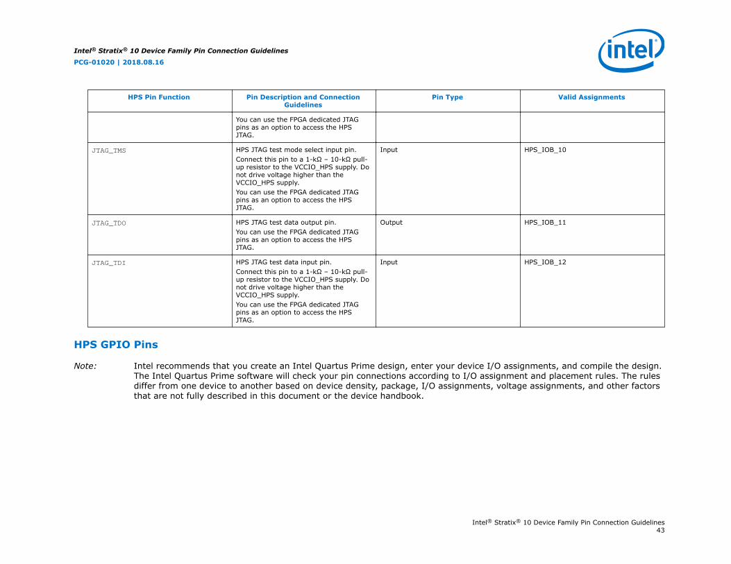
HPS Pin Function Pin Description and ConnectionGuidelines
Pin Type Valid Assignments
You can use the FPGA dedicated JTAGpins as an option to access the HPSJTAG.
JTAG_TMS HPS JTAG test mode select input pin.Connect this pin to a 1-kΩ – 10-kΩ pull-up resistor to the VCCIO_HPS supply. Donot drive voltage higher than theVCCIO_HPS supply.You can use the FPGA dedicated JTAGpins as an option to access the HPSJTAG.
Input HPS_IOB_10
JTAG_TDO HPS JTAG test data output pin.You can use the FPGA dedicated JTAGpins as an option to access the HPSJTAG.
Output HPS_IOB_11
JTAG_TDI HPS JTAG test data input pin.Connect this pin to a 1-kΩ – 10-kΩ pull-up resistor to the VCCIO_HPS supply. Donot drive voltage higher than theVCCIO_HPS supply.You can use the FPGA dedicated JTAGpins as an option to access the HPSJTAG.
Input HPS_IOB_12
HPS GPIO Pins
Note: Intel recommends that you create an Intel Quartus Prime design, enter your device I/O assignments, and compile the design.The Intel Quartus Prime software will check your pin connections according to I/O assignment and placement rules. The rulesdiffer from one device to another based on device density, package, I/O assignments, voltage assignments, and other factorsthat are not fully described in this document or the device handbook.
Intel® Stratix® 10 Device Family Pin Connection Guidelines
PCG-01020 | 2018.08.16
Intel® Stratix® 10 Device Family Pin Connection Guidelines43

Table 20. HPS GPIO Pins—PreliminaryThere are two GPIO controllers (GPIO0 and GPIO1) for the Intel Stratix 10 HPS.
HPS Pin Function Pin Description and ConnectionGuidelines
Pin Type Valid Assignments
GPIO0_IO[0..23] General purpose input output.Ensure that the I/O standard used iscompatible with VCCIO_HPS.
I/O HPS_IOA_[1..24]HPS_IOB_[1..24]
GPIO1_IO[0..23]
HPS SDMMC Pins
Note: Intel recommends that you create an Intel Quartus Prime design, enter your device I/O assignments, and compile the design.The Intel Quartus Prime software will check your pin connections according to I/O assignment and placement rules. The rulesdiffer from one device to another based on device density, package, I/O assignments, voltage assignments, and other factorsthat are not fully described in this document or the device handbook.
Table 21. HPS SDMMC Pins—PreliminaryIntel recommends adding a 1-kΩ to 10-kΩ pull-up resistor to every SDMMC data signal that is used.
HPS Pin Function Pin Description andConnection Guidelines
Pin Type Valid Assignments (select from one of the groups)
Group 1 Group 2
SDMMC_CCLK SDMMC clock out Output HPS_IOA_1 HPS_IOB_15
SDMMC_CMD SDMMC command linePull this pin high on the boardwith a weak pull-up resistor. Forexample, a 10-kΩ toVCCIO_HPS.
I/O HPS_IOA_2 HPS_IOB_14
SDMMC_DATA0 SDMMC Data 0 I/O HPS_IOA_3 HPS_IOB_13
SDMMC_DATA1 SDMMC Data 1 I/O HPS_IOA_4 HPS_IOB_16
SDMMC_DATA2 SDMMC Data 2 I/O HPS_IOA_5 HPS_IOB_17
SDMMC_DATA3 SDMMC Data 3When using SD card, there is anexisting 50-kΩ pull-up onSDMMC Data Bit 3 which can bedisabled in the Intel QuartusPrime software by using the
I/O HPS_IOA_6 HPS_IOB_18
continued...
Intel® Stratix® 10 Device Family Pin Connection Guidelines
PCG-01020 | 2018.08.16
Intel® Stratix® 10 Device Family Pin Connection Guidelines44

HPS Pin Function Pin Description andConnection Guidelines
Pin Type Valid Assignments (select from one of the groups)
Group 1 Group 2
SET_CLR_CARD_DETECT(ACMD42) command. This is notapplicable to the eMMC flash.
SDMMC_DATA4 SDMMC Data 4 I/O HPS_IOA_7 HPS_IOB_19
SDMMC_DATA5 SDMMC Data 5 I/O HPS_IOA_8 HPS_IOB_20
SDMMC_DATA6 SDMMC Data 6 I/O HPS_IOA_9 HPS_IOB_21
SDMMC_DATA7 SDMMC Data 7 I/O HPS_IOA_10 HPS_IOB_22
SDMMC_PWR_EN SDMMC Power Enable Output HPS_IOA_11 HPS_IOB_23
HPS NAND Pins
Note: Intel recommends that you create an Intel Quartus Prime design, enter your device I/O assignments, and compile the design.The Intel Quartus Prime software will check your pin connections according to I/O assignment and placement rules. The rulesdiffer from one device to another based on device density, package, I/O assignments, voltage assignments, and other factorsthat are not fully described in this document or the device handbook.
Table 22. HPS NAND Pins—Preliminary
HPS Pin Functions Pin Description andConnection Guidelines
Pin Type Valid Assignments (select from one of the groups)
Group 1 Group 2
NAND_ADQ0 NAND Data Bit 0 I/O HPS_IOA_1 HPS_IOB_1
NAND_ADQ1 NAND Data Bit 1 I/O HPS_IOA_2 HPS_IOB_2
NAND_WE_N NAND Write EnableSee Note 11 in Notes to IntelStratix 10 SX Pin ConnectionGuidelines.
Output HPS_IOA_3 HPS_IOB_3
NAND_RE_N NAND Read EnableSee Note 11 in Notes to IntelStratix 10 SX Pin ConnectionGuidelines.
Output HPS_IOA_4 HPS_IOB_4
continued...
Intel® Stratix® 10 Device Family Pin Connection Guidelines
PCG-01020 | 2018.08.16
Intel® Stratix® 10 Device Family Pin Connection Guidelines45

HPS Pin Functions Pin Description andConnection Guidelines
Pin Type Valid Assignments (select from one of the groups)
Group 1 Group 2
NAND_WP_N NAND Write Protect Output HPS_IOA_5 HPS_IOB_5
NAND_ADQ2 NAND Data Bit 2 I/O HPS_IOA_6 HPS_IOB_6
NAND_ADQ3 NAND Data Bit 3 I/O HPS_IOA_7 HPS_IOB_7
NAND_CLE NAND Command Latch Enable Output HPS_IOA_8 HPS_IOB_8
NAND_ADQ4 NAND Data Bit 4 I/O HPS_IOA_9 HPS_IOB_9
NAND_ADQ5 NAND Data Bit 5 I/O HPS_IOA_10 HPS_IOB_10
NAND_ADQ6 NAND Data Bit 6 I/O HPS_IOA_11 HPS_IOB_11
NAND_ADQ7 NAND Data Bit 7 I/O HPS_IOA_12 HPS_IOB_12
NAND_ALE NAND Address Latch Enable Output HPS_IOA_13 HPS_IOB_13
NAND_RB NAND Ready/BusyConnect this pin through a 1-kΩto 10-kΩ pull-up resistor toVCCIO_HPS.
Input HPS_IOA_14 HPS_IOB_14
NAND_CE_N NAND Chip EnableSee Note 11 in Notes to IntelStratix 10 SX Pin ConnectionGuidelines.
Output HPS_IOA_15 HPS_IOB_15
NAND_ADQ8 NAND Data Bit 8 I/O HPS_IOA_17 HPS_IOB_17
NAND_ADQ9 NAND Data Bit 9 I/O HPS_IOA_18 HPS_IOB_18
NAND_ADQ10 NAND Data Bit 10 I/O HPS_IOA_19 HPS_IOB_19
NAND_ADQ11 NAND Data Bit 11 I/O HPS_IOA_20 HPS_IOB_20
NAND_ADQ12 NAND Data Bit 12 I/O HPS_IOA_21 HPS_IOB_21
NAND_ADQ13 NAND Data Bit 13 I/O HPS_IOA_22 HPS_IOB_22
NAND_ADQ14 NAND Data Bit 14 I/O HPS_IOA_23 HPS_IOB_23
NAND_ADQ15 NAND Data Bit 15 I/O HPS_IOA_24 HPS_IOB_24
Intel® Stratix® 10 Device Family Pin Connection Guidelines
PCG-01020 | 2018.08.16
Intel® Stratix® 10 Device Family Pin Connection Guidelines46

HPS USB Pins
Note: Intel recommends that you create an Intel Quartus Prime design, enter your device I/O assignments, and compile the design.The Intel Quartus Prime software will check your pin connections according to I/O assignment and placement rules. The rulesdiffer from one device to another based on device density, package, I/O assignments, voltage assignments, and other factorsthat are not fully described in this document or the device handbook.
Table 23. HPS USB Pins—PreliminaryThere are two USB controllers (USB0 and USB1) for the Intel Stratix 10 HPS.
HPS Pin Function Pin Description and ConnectionGuidelines
Pin Type Valid Assignments
USB0_CLK USB0 Clock Input HPS_IOA_1
USB0_STP USB0 Stop Data Output HPS_IOA_2
USB0_DIR USB0 Direction Input HPS_IOA_3
USB0_DATA0 USB0 Data Bit 0 I/O HPS_IOA_4
USB0_DATA1 USB0 Data Bit 1 I/O HPS_IOA_5
USB0_NXT USB0 Next Data Input HPS_IOA_6
USB0_DATA2 USB0 Data Bit 2 I/O HPS_IOA_7
USB0_DATA3 USB0 Data Bit 3 I/O HPS_IOA_8
USB0_DATA4 USB0 Data Bit 4 I/O HPS_IOA_9
USB0_DATA5 USB0 Data Bit 5 I/O HPS_IOA_10
USB0_DATA6 USB0 Data Bit 6 I/O HPS_IOA_11
USB0_DATA7 USB0 Data Bit 7 I/O HPS_IOA_12
USB1_CLK USB1 Clock Input HPS_IOA_13
USB1_STP USB1 Stop Data Output HPS_IOA_14
USB1_DIR USB1 Direction Input HPS_IOA_15
USB1_DATA0 USB1 Data Bit 0 I/O HPS_IOA_16
USB1_DATA1 USB1 Data Bit 1 I/O HPS_IOA_17
continued...
Intel® Stratix® 10 Device Family Pin Connection Guidelines
PCG-01020 | 2018.08.16
Intel® Stratix® 10 Device Family Pin Connection Guidelines47

HPS Pin Function Pin Description and ConnectionGuidelines
Pin Type Valid Assignments
USB1_NXT USB1 Next Data Input HPS_IOA_18
USB1_DATA2 USB1 Data Bit 2 I/O HPS_IOA_19
USB1_DATA3 USB1 Data Bit 3 I/O HPS_IOA_20
USB1_DATA4 USB1 Data Bit 4 I/O HPS_IOA_21
USB1_DATA5 USB1 Data Bit 5 I/O HPS_IOA_22
USB1_DATA6 USB1 Data Bit 6 I/O HPS_IOA_23
USB1_DATA7 USB1 Data Bit 7 I/O HPS_IOA_24
HPS EMAC Pins
Note: Intel recommends that you create an Intel Quartus Prime design, enter your device I/O assignments, and compile the design.The Intel Quartus Prime software will check your pin connections according to I/O assignment and placement rules. The rulesdiffer from one device to another based on device density, package, I/O assignments, voltage assignments, and other factorsthat are not fully described in this document or the device handbook.
Table 24. HPS EMAC Pins—PreliminaryThere are three EMAC controllers (EMAC0, EMAC1, and EMAC2) for the Intel Stratix 10 HPS.
HPS Pin Function Pin Description and ConnectionGuidelines
Pin Type Valid Assignments
EMAC0_TX_CLK EMAC0 Transmit Clock Output HPS_IOA_13
EMAC0_TX_CTL EMAC0 Transmit Control Output HPS_IOA_14
EMAC0_RX_CLK EMAC0 Receive Clock Input HPS_IOA_15
EMAC0_RX_CTL EMAC0 Receive Control Input HPS_IOA_16
EMAC0_TXD0 EMAC0 Transmit Data Bit 0 Output HPS_IOA_17
EMAC0_TXD1 EMAC0 Transmit Data Bit 1 Output HPS_IOA_18
EMAC0_RXD0 EMAC0 Receive Data Bit 0 Input HPS_IOA_19
continued...
Intel® Stratix® 10 Device Family Pin Connection Guidelines
PCG-01020 | 2018.08.16
Intel® Stratix® 10 Device Family Pin Connection Guidelines48

HPS Pin Function Pin Description and ConnectionGuidelines
Pin Type Valid Assignments
EMAC0_RXD1 EMAC0 Receive Data Bit 1 Input HPS_IOA_20
EMAC0_TXD2 EMAC0 Transmit Data Bit 2 Output HPS_IOA_21
EMAC0_TXD3 EMAC0 Transmit Data Bit 3 Output HPS_IOA_22
EMAC0_RXD2 EMAC0 Receive Data Bit 2 Input HPS_IOA_23
EMAC0_RXD3 EMAC0 Receive Data Bit 3 Input HPS_IOA_24
EMAC1_TX_CLK EMAC1 Transmit Clock Output HPS_IOB_1
EMAC1_TX_CTL EMAC1 Transmit Control Output HPS_IOB_2
EMAC1_RX_CLK EMAC1 Receive Clock Input HPS_IOB_3
EMAC1_RX_CTL EMAC1 Receive Control. Input HPS_IOB_4
EMAC1_TXD0 EMAC1 Transmit Data Bit 0 Output HPS_IOB_5
EMAC1_TXD1 EMAC1 Transmit Data Bit 1 Output HPS_IOB_6
EMAC1_RXD0 EMAC1 Receive Data Bit 0 Input HPS_IOB_7
EMAC1_RXD1 EMAC1 Receive Data Bit 1 Input HPS_IOB_8
EMAC1_TXD2 EMAC1 Transmit Data Bit 2 Output HPS_IOB_9
EMAC1_TXD3 EMAC1 Transmit Data Bit 3 Output HPS_IOB_10
EMAC1_RXD2 EMAC1 Receive Data Bit 2 Input HPS_IOB_11
EMAC1_RXD3 EMAC1 Receive Data Bit 3 Input HPS_IOB_12
EMAC2_TX_CLK EMAC2 Transmit Clock Output HPS_IOB_13
EMAC2_TX_CTL EMAC2 Transmit Control Output HPS_IOB_14
EMAC2_RX_CLK EMAC2 Receive Clock Input HPS_IOB_15
EMAC2_RX_CTL EMAC2 Receive Control Input HPS_IOB_16
EMAC2_TXD0 EMAC2 Transmit Data Bit 0 Output HPS_IOB_17
EMAC2_TXD1 EMAC2 Transmit Data Bit 1 Output HPS_IOB_18
continued...
Intel® Stratix® 10 Device Family Pin Connection Guidelines
PCG-01020 | 2018.08.16
Intel® Stratix® 10 Device Family Pin Connection Guidelines49
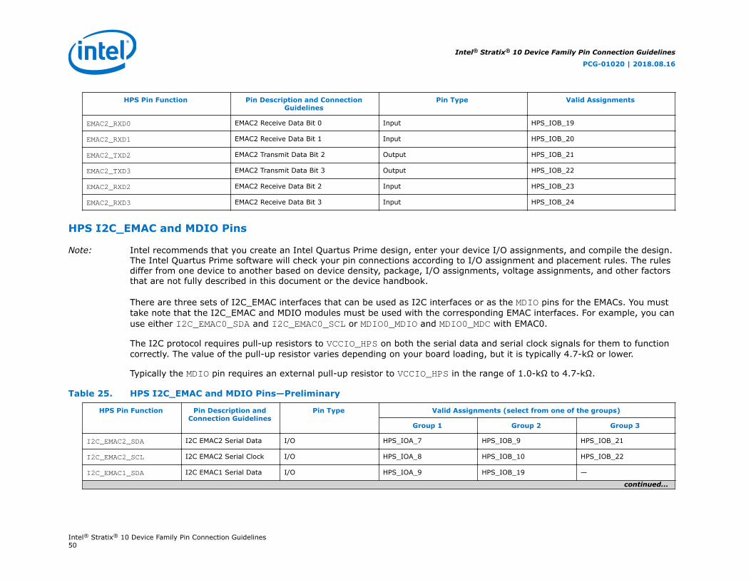
HPS Pin Function Pin Description and ConnectionGuidelines
Pin Type Valid Assignments
EMAC2_RXD0 EMAC2 Receive Data Bit 0 Input HPS_IOB_19
EMAC2_RXD1 EMAC2 Receive Data Bit 1 Input HPS_IOB_20
EMAC2_TXD2 EMAC2 Transmit Data Bit 2 Output HPS_IOB_21
EMAC2_TXD3 EMAC2 Transmit Data Bit 3 Output HPS_IOB_22
EMAC2_RXD2 EMAC2 Receive Data Bit 2 Input HPS_IOB_23
EMAC2_RXD3 EMAC2 Receive Data Bit 3 Input HPS_IOB_24
HPS I2C_EMAC and MDIO Pins
Note: Intel recommends that you create an Intel Quartus Prime design, enter your device I/O assignments, and compile the design.The Intel Quartus Prime software will check your pin connections according to I/O assignment and placement rules. The rulesdiffer from one device to another based on device density, package, I/O assignments, voltage assignments, and other factorsthat are not fully described in this document or the device handbook.
There are three sets of I2C_EMAC interfaces that can be used as I2C interfaces or as the MDIO pins for the EMACs. You musttake note that the I2C_EMAC and MDIO modules must be used with the corresponding EMAC interfaces. For example, you canuse either I2C_EMAC0_SDA and I2C_EMAC0_SCL or MDIO0_MDIO and MDIO0_MDC with EMAC0.
The I2C protocol requires pull-up resistors to VCCIO_HPS on both the serial data and serial clock signals for them to functioncorrectly. The value of the pull-up resistor varies depending on your board loading, but it is typically 4.7-kΩ or lower.
Typically the MDIO pin requires an external pull-up resistor to VCCIO_HPS in the range of 1.0-kΩ to 4.7-kΩ.
Table 25. HPS I2C_EMAC and MDIO Pins—Preliminary
HPS Pin Function Pin Description andConnection Guidelines
Pin Type Valid Assignments (select from one of the groups)
Group 1 Group 2 Group 3
I2C_EMAC2_SDA I2C EMAC2 Serial Data I/O HPS_IOA_7 HPS_IOB_9 HPS_IOB_21
I2C_EMAC2_SCL I2C EMAC2 Serial Clock I/O HPS_IOA_8 HPS_IOB_10 HPS_IOB_22
I2C_EMAC1_SDA I2C EMAC1 Serial Data I/O HPS_IOA_9 HPS_IOB_19 —
continued...
Intel® Stratix® 10 Device Family Pin Connection Guidelines
PCG-01020 | 2018.08.16
Intel® Stratix® 10 Device Family Pin Connection Guidelines50
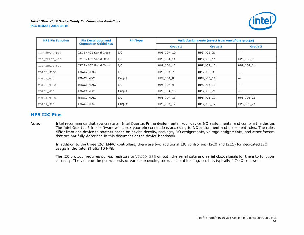
HPS Pin Function Pin Description andConnection Guidelines
Pin Type Valid Assignments (select from one of the groups)
Group 1 Group 2 Group 3
I2C_EMAC1_SCL I2C EMAC1 Serial Clock I/O HPS_IOA_10 HPS_IOB_20 —
I2C_EMAC0_SDA I2C EMAC0 Serial Data I/O HPS_IOA_11 HPS_IOB_11 HPS_IOB_23
I2C_EMAC0_SCL I2C EMAC0 Serial Clock I/O HPS_IOA_12 HPS_IOB_12 HPS_IOB_24
MDIO2_MDIO EMAC2 MDIO I/O HPS_IOA_7 HPS_IOB_9 —
MDIO2_MDC EMAC2 MDC Output HPS_IOA_8 HPS_IOB_10 —
MDIO1_MDIO EMAC1 MDIO I/O HPS_IOA_9 HPS_IOB_19 —
MDIO1_MDC EMAC1 MDC Output HPS_IOA_10 HPS_IOB_20 —
MDIO0_MDIO EMAC0 MDIO I/O HPS_IOA_11 HPS_IOB_11 HPS_IOB_23
MDIO0_MDC EMAC0 MDC Output HPS_IOA_12 HPS_IOB_12 HPS_IOB_24
HPS I2C Pins
Note: Intel recommends that you create an Intel Quartus Prime design, enter your device I/O assignments, and compile the design.The Intel Quartus Prime software will check your pin connections according to I/O assignment and placement rules. The rulesdiffer from one device to another based on device density, package, I/O assignments, voltage assignments, and other factorsthat are not fully described in this document or the device handbook.
In addition to the three I2C_EMAC controllers, there are two additional I2C controllers (I2C0 and I2C1) for dedicated I2Cusage in the Intel Stratix 10 HPS.
The I2C protocol requires pull-up resistors to VCCIO_HPS on both the serial data and serial clock signals for them to functioncorrectly. The value of the pull-up resistor varies depending on your board loading, but it is typically 4.7-kΩ or lower.
Intel® Stratix® 10 Device Family Pin Connection Guidelines
PCG-01020 | 2018.08.16
Intel® Stratix® 10 Device Family Pin Connection Guidelines51

Table 26. HPS I2C Pins—Preliminary
HPS Pin Function Pin Description andConnectionGuidelines
Pin Type Valid Assignments (select from one of the groups)
Group 1 Group 2 Group 3 Group 4
I2C0 _SDA I2C0 Serial Data I/O HPS_IOA_5 HPS_IOA_23 HPS_IOB_3 —
I2C0 _SCL I2C0 Serial Clock I/O HPS_IOA_6 HPS_IOA_24 HPS_IOB_4 —
I2C1 _SDA I2C1 Serial Data I/O HPS_IOA_3 HPS_IOA_21 HPS_IOB_7 HPS_IOB_13
I2C1 _SCL I2C1 Serial Clock I/O HPS_IOA_4 HPS_IOA_22 HPS_IOB_8 HPS_IOB_14
HPS SPI Pins
Note: Intel recommends that you create an Intel Quartus Prime design, enter your device I/O assignments, and compile the design.The Intel Quartus Prime software will check your pin connections according to I/O assignment and placement rules. The rulesdiffer from one device to another based on device density, package, I/O assignments, voltage assignments, and other factorsthat are not fully described in this document or the device handbook.
Table 27. HPS SPI Pins—PreliminaryThere are two SPI Master (SPIM0 and SPIM1) and two SPI Slave (SPIS0 and SPIS1) controllers for the Intel Stratix 10 HPS.
HPS Pin Function Pin Description andConnection Guidelines
Pin Type Valid Assignments (select from one of the group)
Group 1 Group 2 Group 3
SPIM0_CLK SPIM0 Clock Output HPS_IOA_5 HPS_IOB_21 HPS_IOB_21
SPIM0_MOSI SPIM0 Master Out Slave In Output HPS_IOA_6 HPS_IOB_22 HPS_IOB_22
SPIM0_MISO SPIM0 Master In Slave Out Input HPS_IOA_7 HPS_IOB_19 HPS_IOB_23
SPIM0_SS0_N SPIM0 Slave Select 0See Note 11 in Notes toIntel Stratix 10 SX PinConnection Guidelines.
Output HPS_IOA_8 HPS_IOB_20 HPS_IOB_24
SPIM0_SS1_N SPIM0 Slave Select 1See Note 11 in Notes toIntel Stratix 10 SX PinConnection Guidelines.
Output HPS_IOA_1 HPS_IOB_18 HPS_IOB_18
continued...
Intel® Stratix® 10 Device Family Pin Connection Guidelines
PCG-01020 | 2018.08.16
Intel® Stratix® 10 Device Family Pin Connection Guidelines52
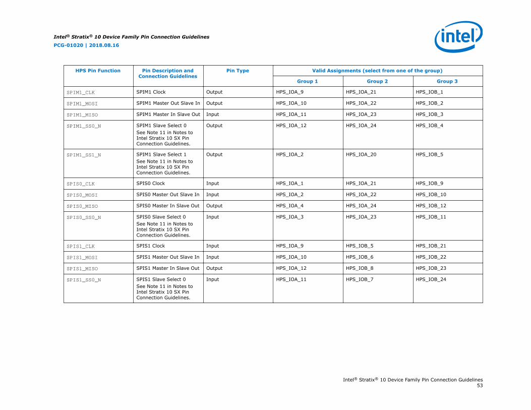
HPS Pin Function Pin Description andConnection Guidelines
Pin Type Valid Assignments (select from one of the group)
Group 1 Group 2 Group 3
SPIM1_CLK SPIM1 Clock Output HPS_IOA_9 HPS_IOA_21 HPS_IOB_1
SPIM1_MOSI SPIM1 Master Out Slave In Output HPS_IOA_10 HPS_IOA_22 HPS_IOB_2
SPIM1_MISO SPIM1 Master In Slave Out Input HPS_IOA_11 HPS_IOA_23 HPS_IOB_3
SPIM1_SS0_N SPIM1 Slave Select 0See Note 11 in Notes toIntel Stratix 10 SX PinConnection Guidelines.
Output HPS_IOA_12 HPS_IOA_24 HPS_IOB_4
SPIM1_SS1_N SPIM1 Slave Select 1See Note 11 in Notes toIntel Stratix 10 SX PinConnection Guidelines.
Output HPS_IOA_2 HPS_IOA_20 HPS_IOB_5
SPIS0_CLK SPIS0 Clock Input HPS_IOA_1 HPS_IOA_21 HPS_IOB_9
SPIS0_MOSI SPIS0 Master Out Slave In Input HPS_IOA_2 HPS_IOA_22 HPS_IOB_10
SPIS0_MISO SPIS0 Master In Slave Out Output HPS_IOA_4 HPS_IOA_24 HPS_IOB_12
SPIS0_SS0_N SPIS0 Slave Select 0See Note 11 in Notes toIntel Stratix 10 SX PinConnection Guidelines.
Input HPS_IOA_3 HPS_IOA_23 HPS_IOB_11
SPIS1_CLK SPIS1 Clock Input HPS_IOA_9 HPS_IOB_5 HPS_IOB_21
SPIS1_MOSI SPIS1 Master Out Slave In Input HPS_IOA_10 HPS_IOB_6 HPS_IOB_22
SPIS1_MISO SPIS1 Master In Slave Out Output HPS_IOA_12 HPS_IOB_8 HPS_IOB_23
SPIS1_SS0_N SPIS1 Slave Select 0See Note 11 in Notes toIntel Stratix 10 SX PinConnection Guidelines.
Input HPS_IOA_11 HPS_IOB_7 HPS_IOB_24
Intel® Stratix® 10 Device Family Pin Connection Guidelines
PCG-01020 | 2018.08.16
Intel® Stratix® 10 Device Family Pin Connection Guidelines53

HPS UART Pins
Note: Intel recommends that you create an Intel Quartus Prime design, enter your device I/O assignments, and compile the design.The Intel Quartus Prime software will check your pin connections according to I/O assignment and placement rules. The rulesdiffer from one device to another based on device density, package, I/O assignments, voltage assignments, and other factorsthat are not fully described in this document or the device handbook.
Table 28. HPS UART Pins—PreliminaryThere are two UART (UART0 and UART1) controllers for the Intel Stratix 10 HPS.
HPS Pin Function Pin Description andConnection Guidelines
Pin Type Valid Assignments (select from one of the groups)
Group 1 Group 2 Group 3
UART0_CTS_N UART0 Clear to SendSee Note 11 in Notes toIntel Stratix 10 SX PinConnection Guidelines.
Input HPS_IOA_1 HPS_IOA_21 HPS_IOB_1
UART0_RTS_N UART0 Request to SendSee Note 11 in Notes toIntel Stratix 10 SX PinConnection Guidelines.
Output HPS_IOA_2 HPS_IOA_22 HPS_IOB_2
UART0_TX UART0 Transmit Output HPS_IOA_3 HPS_IOA_23 HPS_IOB_3
UART0_RX UART0 Receive Input HPS_IOA_4 HPS_IOA_24 HPS_IOB_4
UART1_CTS_N UART1 Clear to SendSee Note 11 in Notes toIntel Stratix 10 SX PinConnection Guidelines.
Input HPS_IOA_5 HPS_IOB_5 HPS_IOB_17
UART1_RTS_N UART1 Request to SendSee Note 11 in Notes toIntel Stratix 10 SX PinConnection Guidelines.
Output HPS_IOA_6 HPS_IOB_6 HPS_IOB_18
UART1_TX UART1 Transmit Output HPS_IOA_7 HPS_IOB_7 HPS_IOB_15
UART1_RX UART1 Receive Input HPS_IOA_8 HPS_IOB_8 HPS_IOB_16
Intel® Stratix® 10 Device Family Pin Connection Guidelines
PCG-01020 | 2018.08.16
Intel® Stratix® 10 Device Family Pin Connection Guidelines54

HPS Trace Pins
Note: Intel recommends that you create an Intel Quartus Prime design, enter your device I/O assignments, and compile the design.The Intel Quartus Prime software will check your pin connections according to I/O assignment and placement rules. The rulesdiffer from one device to another based on device density, package, I/O assignments, voltage assignments, and other factorsthat are not fully described in this document or the device handbook.
Table 29. HPS Trace Pins—PreliminaryYou can select up to 16 trace output pins in the Intel Stratix 10 HPS. These pins do not have to be located in the same quadrant.
HPS Pin Function Pin Description and ConnectionGuidelines
Pin Type Valid Assignments
Trace_CLK Trace Clock Output HPS_IOA_20
HPS_IOB_20
Trace_D0 Trace Data 0 Output HPS_IOA_21
HPS_IOB_21
Trace_D1 Trace Data 1 Output HPS_IOA_22
HPS_IOB_22
Trace_D2 Trace Data 2 Output HPS_IOA_23
HPS_IOB_23
Trace_D3 Trace Data 3 Output HPS_IOA_24
HPS_IOB_24
Trace_D4 Trace Data 4 Output HPS_IOA_19
HPS_IOA_7
HPS_IOB_19
HPS_IOB_7
Trace_D5 Trace Data 5 Output HPS_IOA_18
HPS_IOA_6
HPS_IOB_18
continued...
Intel® Stratix® 10 Device Family Pin Connection Guidelines
PCG-01020 | 2018.08.16
Intel® Stratix® 10 Device Family Pin Connection Guidelines55

HPS Pin Function Pin Description and ConnectionGuidelines
Pin Type Valid Assignments
HPS_IOB_6
Trace_D6 Trace Data 6 Output HPS_IOA_17
HPS_IOA_5
HPS_IOB_17
HPS_IOB_5
Trace_D7 Trace Data 7 Output HPS_IOA_16
HPS_IOA_4
HPS_IOB_16
HPS_IOB_4
Trace_D8 Trace Data 8 Output HPS_IOA_15
HPS_IOA_3
HPS_IOB_15
HPS_IOB_3
Trace_D9 Trace Data 9 Output HPS_IOA_14
HPS_IOA_2
HPS_IOB_14
HPS_IOB_2
Trace_D10 Trace Data 10 Output HPS_IOA_13
HPS_IOA_1
HPS_IOB_13
HPS_IOB_1
Trace_D11 Trace Data 11 Output HPS_IOA_12
HPS_IOB_12
Trace_D12 Trace Data 12 Output HPS_IOA_11
continued...
Intel® Stratix® 10 Device Family Pin Connection Guidelines
PCG-01020 | 2018.08.16
Intel® Stratix® 10 Device Family Pin Connection Guidelines56

HPS Pin Function Pin Description and ConnectionGuidelines
Pin Type Valid Assignments
HPS_IOB_11
Trace_D13 Trace Data 13 Output HPS_IOA_10
HPS_IOB_10
Trace_D14 Trace Data 14 Output HPS_IOA_9
HPS_IOB_9
Trace_D15 Trace Data 15 Output HPS_IOA_8
HPS_IOB_8
Notes to Intel Stratix 10 SX Pin Connection Guidelines
Note: Intel recommends that you create an Intel Quartus Prime design, enter your device I/O assignments, and compile the design.The Intel Quartus Prime software will check your pin connections according to I/O assignment and placement rules. The rulesdiffer from one device to another based on device density, package, I/O assignments, voltage assignments, and other factorsthat are not fully described in this document or the device handbook.
Intel provides these guidelines only as recommendations. It is the responsibility of the designer to apply simulation results tothe design to verify proper device functionality.
1. These pin connection guidelines are based on the Intel Stratix 10 SX device variant.
2. Select the capacitance values for the power supply after you consider the amount of power they need to supply over thefrequency of operation of the particular circuit being decoupled. Calculate the target impedance for the power plane basedon current draw and voltage drop requirements of the device/supply. Then, decouple the power plane using theappropriate number of capacitors. On-board capacitors do not decouple higher than 100 MHz due to “Equivalent SeriesInductance” of the mounting of the packages. Consider proper board design techniques such as interplane capacitancewith low inductance for higher frequency decoupling. Refer to the PDN tool.
3. Use the Intel Stratix 10 Early Power Estimator (EPE) to determine the preliminary current requirements for VCC and otherpower supplies. Use the Intel Quartus Prime Power Analyzer for the most accurate current requirements for this and otherpower supplies.
4. These supplies may share power planes across multiple Intel Stratix 10 devices.
5. Power pins should not share breakout vias from the BGA. Each ball on the BGA must have its own dedicated breakout via.
Intel® Stratix® 10 Device Family Pin Connection Guidelines
PCG-01020 | 2018.08.16
Intel® Stratix® 10 Device Family Pin Connection Guidelines57

6. Low Noise Switching Regulator - a switching regulator circuit encapsulated in a thin surface mount package containing theswitch controller, power FETs, inductor, and other support components. The switching frequency is usually between 800kHz and 1 MHz and has fast transient response. The switching frequency range is not an Intel requirement.
7. The number of modular I/O banks on Intel Stratix 10 devices depends on the device density. For the indexes available fora specific device, refer to the I/O Bank section in the Intel Stratix 10 General Purpose I/O User Guide.
8. For AC-coupled links, the AC-coupling capacitor can be placed anywhere along the channel. PCI Express protocol requiresthat the AC-coupling capacitor is placed on the transmitter side of the interface that permits adapters to be plugged andunplugged.
9. For item [#], refer to the device pin table for the pin-out mapping.
10. The peripheral pins are programmable through pin multiplexors. Each pin may have multiple functions. HPS and SDMdedicated I/O pin multiplexing is programmable using the Quartus Prime software. The pin mux determines how the pinsare used.
11. These pins are inverted or active-low signals.
12. Example 3 through Example 6 illustrate the power supply sharing guidelines for the Intel Stratix 10 SX devices.
Power Supply Sharing Guidelines for Intel Stratix 10 Devices
Intel Stratix 10 devices have specific power-up and power-down sequence requirements. For more information, refer to theAN692: Power Sequencing Considerations for Intel Cyclone® 10 GX, Intel Arria® 10, and Intel Stratix 10 Devices and IntelStratix 10 Power Management User Guide.
Related Information
• AN692: Power Sequencing Considerations for Intel Cyclone 10 GX, Intel Arria 10, and Intel Stratix 10 Devices
• Intel Stratix 10 Power Management User Guide
Intel® Stratix® 10 Device Family Pin Connection Guidelines
PCG-01020 | 2018.08.16
Intel® Stratix® 10 Device Family Pin Connection Guidelines58

Example 1—Intel Stratix 10 GX
Table 30. Power Supply Sharing Guidelines for Intel Stratix 10 GX with Transceiver Data Rate <= 15 Gbps—PreliminaryExample Requiring 5 Power Regulators
Power Pin Name Regulator Group Voltage Level (V) Supply Tolerance Power Source Regulator Sharing Notes
VCC 1 0.80.85
SmartVID
± 30mV Switcher (*) Share Source VCC and VCCP from the sameregulator, sharing the same voltageplane.VCCP
VCCERAM 2 0.9 ± 30mV Switcher (*) Share Connect the VCCERAM to a dedicated0.9V power supply. You may connect theVCCPLLDIG_SDM power to the VCCERAMpower plane with proper isolationfiltering.When implementing a filtered supplytopology, you must consider the IR dropacross the filter.
VCCPLLDIG_SDM Filter
VCCR_GXB[L,R] 3 1.03 ± 30mV Switcher (*) Share You have the option to source theVCCR_GXB and VCCT_GXB from thesame regulator when all the power railsrequire the same voltage level. For betterperformance and in order to meet PCIeGen 3 jitter specifications, isolateVCCR_GXB and VCCT_GXB from eachother with at least 30dB of isolation for a1MHz to 100MHz bandwidth.
VCCT_GXB[L,R]
VCCPT 4 1.8 ± 5% (**) Switcher (*) Share if 1.8V You may source VCCPT and VCCIO_SDMfrom the same regulator. You mayconnect the VCCIO, VCCIO3V, andVCCBAT to the same power plane if thethose power rails are at the same voltagelevel. You may also connect theVCCH_GXB, VCCA_PLL, VCCPLL_SDM,and VCCADC to the same power planewith proper isolation filtering. Dependingon the regulator capabilities, you havethe option to share this supply withmultiple Intel Stratix 10 devices.
VCCIO_SDM 1.8
VCCIO Varies
VCCIO3V Varies
VCCBAT Varies
VCCH_GXB[L,R] 1.8 Filter
VCCA_PLL 1.8
VCCPLL_SDM 1.8
continued...
Intel® Stratix® 10 Device Family Pin Connection Guidelines
PCG-01020 | 2018.08.16
Intel® Stratix® 10 Device Family Pin Connection Guidelines59

Power Pin Name Regulator Group Voltage Level (V) Supply Tolerance Power Source Regulator Sharing Notes
When implementing a filtered supplytopology, you must consider the IR dropacross the filter.
VCCADC 1.8
VCCFUSEWR_SDM 5 2.4 ± 50mV Switcher (*) Isolate Connect VCCFUSEWR_SDM to adedicated 2.4V power supply if the SDMfuses need to be written. LeaveVCCFUSEWR_SDM unconnected or tie itto VCCPT 1.8V power if the SDM fuses donot need to be written. Do not tie this pinto GND.
(*)When using a switcher to supply these voltages, the switcher must be a low noise switcher as defined in note 7 of theNotes to Intel Stratix 10 GX Pin Connection Guidelines.
(**)The supported tolerance for the VCCIO power supply varies depending on the I/O standards. For more details, refer tothe I/O standard specification in the Intel Stratix 10 Device Datasheet. Use the EPE (Early Power Estimator) and the IntelQuartus Prime Power Analyzer tool to assist in determining the power required for your specific design.
Each board design requires its own power analysis to determine the required power regulators needed to satisfy the specificboard design requirements. An example block diagram using the Intel Stratix 10 GX device is provided in Figure 1.
The voltage level for each power rail is preliminary.
Intel® Stratix® 10 Device Family Pin Connection Guidelines
PCG-01020 | 2018.08.16
Intel® Stratix® 10 Device Family Pin Connection Guidelines60

Figure 1. Example Power Supply Sharing Guidelines for Intel Stratix 10 GX with Transceiver Data Rate ≤ 15 Gbps—Preliminary
0.8V, 0.85V, SmartVID (0.8V-0.94V)DC InputBoard Supply
Switcher(*) VCCVCCP
1
0.9VSwitcher(*)
1.8VSwitcher(*)
VCCERAM
VCCR_GXBVCCT_GXB
VCCPTVCCBATVCCIO_SDMVCCIO (1), (2), (3)VCCIO3V (1), (2), (3)
2.4VSwitcher(*)
2
1.03V3
4
5 VCCFUSEWR_SDM
Notes:(1) For all VCCIO and VCCIO3V banks that are 1.8V, all the VCCIO and VCCIO3V banks can share the same 1.8-V regulator with the Group 2 power rails. (2) For all VCCIO and VCCIO3V banks that are 1.8V and driven from a separate regulator, then they need to be in the Group 3 power rails.(3) For all VCCIO and VCCIO3V banks other than 1.8V, they need to be in the Group 3 power rails.(4) When a -V device is used, you must enable the SmartVID connection between the device and the VCC voltage regulator. For more information, refer to the connection guidelines of thePWRMGT_SCL, PWRMGT_SDA, and PWRMGT_ALERT pin function.
Filter VCCPLLDIG_SDM
VCCH_GXBVCCA_PLLVCCPLL_SDMVCCADC
Filter
Switcher(*)
Legend:Power Group 1 - GreenPower Group 2 - RedPower Group 3 - Blue
Intel® Stratix® 10 Device Family Pin Connection Guidelines
PCG-01020 | 2018.08.16
Intel® Stratix® 10 Device Family Pin Connection Guidelines61

Example 2—Intel Stratix 10 GX
Table 31. Power Supply Sharing Guidelines for Intel Stratix 10 GX with 15 Gbps < Transceiver Data Rate <= 28.3 Gbps—PreliminaryExample Requiring 6 Power Regulators
Power Pin Name Regulator Group Voltage Level (V) Supply Tolerance Power Source Regulator Sharing Notes
VCC 1 0.80.85
SmartVID
± 30mV Switcher (*) Share Source VCC and VCCP from the sameregulator, sharing the same voltageplane.VCCP
VCCERAM 2 0.9 ± 30mV Switcher (*) Isolate Connect the VCCERAM to a dedicated0.9V power supply. You may connect theVCCPLLDIG_SDM power to the VCCERAMpower plane with proper isolationfiltering.When implementing a filtered supplytopology, you must consider the IR dropacross the filter.
VCCPLLDIG_SDM Filter
VCCR_GXB[L,R] 3 1.12 ± 20mV Switcher (*) Isolate Connect the VCCR_GXB to a dedicated1.12V power supply.
VCCT_GXB[L,R] 4 1.12 ± 20mV Switcher (*) Isolate Connect the VCCT_GXB to a dedicated1.12V power supply.
continued...
Intel® Stratix® 10 Device Family Pin Connection Guidelines
PCG-01020 | 2018.08.16
Intel® Stratix® 10 Device Family Pin Connection Guidelines62

Power Pin Name Regulator Group Voltage Level (V) Supply Tolerance Power Source Regulator Sharing Notes
VCCPT 5 1.8 ± 5% (**) Switcher (*) Share if 1.8V You may source VCCPT and VCCIO_SDMfrom the same regulator. You mayconnect the VCCIO, VCCIO3V, andVCCBAT to the same power plane if thethose power rails are at the same voltagelevel. You may also connect theVCCH_GXB, VCCA_PLL, VCCPLL_SDM,and VCCADC to the same power planewith proper isolation filtering. Dependingon the regulator capabilities, you havethe option to share this supply withmultiple Intel Stratix 10 devices.When implementing a filtered supplytopology, you must consider the IR dropacross the filter.
VCCIO_SDM 1.8
VCCIO Varies
VCCIO3V Varies
VCCBAT Varies
VCCH_GXB[L,R] 1.8 Filter
VCCA_PLL 1.8
VCCPLL_SDM 1.8
VCCADC 1.8
VCCFUSEWR_SDM 6 2.4 ± 50mV Switcher (*) Isolate Connect VCCFUSEWR_SDM to adedicated 2.4V power supply if the SDMfuses need to be written. LeaveVCCFUSEWR_SDM unconnected or tie itto VCCPT 1.8V power if the SDM fuses donot need to be written. Do not tie this pinto GND.
(*)When using a switcher to supply these voltages, the switcher must be a low noise switcher as defined in note 7 of theNotes to Intel Stratix 10 GX Pin Connection Guidelines.
(**)The supported tolerance for the VCCIO power supply varies depending on the I/O standards. For more details, refer tothe I/O standard specification in the Intel Stratix 10 Device Datasheet. Use the EPE (Early Power Estimator) and the IntelQuartus Prime Power Analyzer tool to assist in determining the power required for your specific design.
Each board design requires its own power analysis to determine the required power regulators needed to satisfy the specificboard design requirements. An example block diagram using the Intel Stratix 10 GX device is provided in Figure 2.
The voltage level for each power rail is preliminary.
Intel® Stratix® 10 Device Family Pin Connection Guidelines
PCG-01020 | 2018.08.16
Intel® Stratix® 10 Device Family Pin Connection Guidelines63

Figure 2. Example Power Supply Sharing Guidelines for Intel Stratix 10 GX with 15 Gbps < Transceiver Data Rate ≤ 28.3Gbps—Preliminary
0.8V, 0.85V, SmartVID (0.8V-0.94V)DC InputBoard Supply
Switcher(*) VCCVCCP
1
0.9VSwitcher(*)
1.8VSwitcher(*)
VCCERAM
VCCR_GXB
VCCPTVCCBATVCCIO_SDMVCCIO (1), (2), (3)VCCIO3V (1), (2), (3)
2.4VSwitcher(*)
2
1.12V3
5
6 VCCFUSEWR_SDM
Filter VCCPLLDIG_SDM
VCCH_GXBVCCA_PLLVCCPLL_SDMVCCADC
Filter
Switcher(*)
VCCT_GXB1.12V4 Switcher(*)
Notes:(1) For all VCCIO and VCCIO3V banks that are 1.8V, all the VCCIO and VCCIO3V banks can share the same 1.8-V regulator with the Group 2 power rails. (2) For all VCCIO and VCCIO3V banks that are 1.8V and driven from a separate regulator, then they need to be in the Group 3 power rails.(3) For all VCCIO and VCCIO3V banks other than 1.8V, they need to be in the Group 3 power rails.(4) When a -V device is used, you must enable the SmartVID connection between the device and the VCC voltage regulator. For more information, refer to the connection guidelines of thePWRMGT_SCL, PWRMGT_SDA, and PWRMGT_ALERT pin function.
Legend:Power Group 1 - GreenPower Group 2 - RedPower Group 3 - Blue
Intel® Stratix® 10 Device Family Pin Connection Guidelines
PCG-01020 | 2018.08.16
Intel® Stratix® 10 Device Family Pin Connection Guidelines64

Example 3—Intel Stratix 10 SX (–1V, –2V, and –3V parts)
Table 32. Power Supply Sharing Guidelines for Intel Stratix 10 SX (–1V, –2V, and –3V parts) with Transceiver Data Rate<= 15 Gbps—PreliminaryExample Requiring 5 Power Regulators
Power Pin Name Regulator Group Voltage Level (V) Supply Tolerance Power Source Regulator Sharing Notes
VCC 1 SmartVID ± 30mV Switcher (*) Share Source VCC and VCCP from the sameregulator, sharing the same voltageplane. You have the option to connectVCCL_HPS to the same regulator as VCCand VCCP when the power rails requirethe same voltage level. You may alsoconnect the VCCPLLDIG_HPS power tothe shared VCC, VCCP, and VCCL_HPSpower planes with proper isolationfiltering.When implementing a filtered supplytopology, you must consider the IR dropacross the filter.If you do not intend to utilize the HPS inthe Intel Stratix 10 SX device, you muststill provide power to the HPS powersupply. Do not leave the VCCL_HPS andVCCPLLDIG_HPS floating or connectthem to GND.
VCCP
VCCL_HPS
VCCPLLDIG_HPS Filter
VCCERAM 2 0.9 ± 30mV Switcher (*) Isolate Connect the VCCERAM to a dedicated0.9V power supply. You may connect theVCCPLLDIG_SDM power to the VCCERAMpower plane with proper isolationfiltering.When implementing a filtered supplytopology, you must consider the IR dropacross the filter.
VCCPLLDIG_SDM Filter
VCCR_GXB[L,R] 3 1.03 ± 30mV Switcher (*) Share You have the option to source theVCCR_GXB and VCCT_GXB from thesame regulator when all the power railsrequire the same voltage level. For betterperformance and in order to meet PCIeGen 3 jitter specifications, isolateVCCR_GXB and VCCT_GXB from eachother with at least 30dB of isolation for a1MHz to 100MHz bandwidth.
VCCT_GXB[L,R]
continued...
Intel® Stratix® 10 Device Family Pin Connection Guidelines
PCG-01020 | 2018.08.16
Intel® Stratix® 10 Device Family Pin Connection Guidelines65
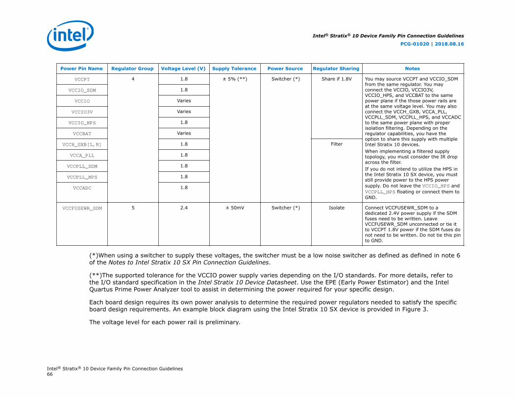
Power Pin Name Regulator Group Voltage Level (V) Supply Tolerance Power Source Regulator Sharing Notes
VCCPT 4 1.8 ± 5% (**) Switcher (*) Share if 1.8V You may source VCCPT and VCCIO_SDMfrom the same regulator. You mayconnect the VCCIO, VCCIO3V,VCCIO_HPS, and VCCBAT to the samepower plane if the those power rails areat the same voltage level. You may alsoconnect the VCCH_GXB, VCCA_PLL,VCCPLL_SDM, VCCPLL_HPS, and VCCADCto the same power plane with properisolation filtering. Depending on theregulator capabilities, you have theoption to share this supply with multipleIntel Stratix 10 devices.When implementing a filtered supplytopology, you must consider the IR dropacross the filter.If you do not intend to utilize the HPS inthe Intel Stratix 10 SX device, you muststill provide power to the HPS powersupply. Do not leave the VCCIO_HPS andVCCPLL_HPS floating or connect them toGND.
VCCIO_SDM 1.8
VCCIO Varies
VCCIO3V Varies
VCCIO_HPS 1.8
VCCBAT Varies
VCCH_GXB[L,R] 1.8 Filter
VCCA_PLL 1.8
VCCPLL_SDM 1.8
VCCPLL_HPS 1.8
VCCADC 1.8
VCCFUSEWR_SDM 5 2.4 ± 50mV Switcher (*) Isolate Connect VCCFUSEWR_SDM to adedicated 2.4V power supply if the SDMfuses need to be written. LeaveVCCFUSEWR_SDM unconnected or tie itto VCCPT 1.8V power if the SDM fuses donot need to be written. Do not tie this pinto GND.
(*)When using a switcher to supply these voltages, the switcher must be a low noise switcher as defined as defined in note 6of the Notes to Intel Stratix 10 SX Pin Connection Guidelines.
(**)The supported tolerance for the VCCIO power supply varies depending on the I/O standards. For more details, refer tothe I/O standard specification in the Intel Stratix 10 Device Datasheet. Use the EPE (Early Power Estimator) and the IntelQuartus Prime Power Analyzer tool to assist in determining the power required for your specific design.
Each board design requires its own power analysis to determine the required power regulators needed to satisfy the specificboard design requirements. An example block diagram using the Intel Stratix 10 SX device is provided in Figure 3.
The voltage level for each power rail is preliminary.
Intel® Stratix® 10 Device Family Pin Connection Guidelines
PCG-01020 | 2018.08.16
Intel® Stratix® 10 Device Family Pin Connection Guidelines66

Figure 3. Example Power Supply Sharing Guidelines for Intel Stratix 10 SX (–1V, –2V, and –3V parts) with TransceiverData Rate <= 15 Gbps—Preliminary
SmartVID (0.8V-0.94V)DC InputBoard Supply
Switcher(*)VCCVCCPVCCL_HPS (1)
1
0.9VSwitcher(*)
1.8VSwitcher(*)
VCCERAM
VCCR_GXBVCCT_GXB
VCCPTVCCBATVCCIO_SDMVCCIO_HPSVCCIO (2), (3), (4)VCCIO3V (2), (3), (4)
2.4VSwitcher(*)
2
1.03V3
4
5 VCCFUSEWR_SDM
Filter VCCPLLDIG_SDM
Filter VCCPLLDIG_HPS (1)
VCCH_GXBVCCA_PLLVCCPLL_SDMVCCPLL_HPSVCCADC
Filter
Switcher(*)
Notes:(1) VCCL_HPS and VCCPLLDIG_HPS can run at 0.94V for higher performance. In this case, these voltages need to run from its own dedicated voltage regulator.Optionally, you can connect VCCL_HPS and VCCPLLDIG_HPS to a fixed 0.9V. If you are connecting VCCL_HPS and VCCPLLDIG_HPS to 0.9V, they can share thesame power regulator with VCCERAM.(2) For all VCCIO and VCCIO3V banks that are 1.8V, all the VCCIO and VCCIO3V banks can share the same 1.8-V regulator with the Group 2 power rails. (3) For all VCCIO and VCCIO3V banks that are 1.8V and driven from a separate regulator, then they need to be in the Group 3 power rails.(4) For all VCCIO and VCCIO3V banks other than 1.8V, they need to be in the Group 3 power rails.(5) When a -V device is used, you must enable the SmartVID connection between the device and the VCC voltage regulator. For more information, refer to the connection guidelines of thePWRMGT_SCL, PWRMGT_SDA, and PWRMGT_ALERT pin function.
Legend:Power Group 1 - GreenPower Group 2 - RedPower Group 3 - Blue
Intel® Stratix® 10 Device Family Pin Connection Guidelines
PCG-01020 | 2018.08.16
Intel® Stratix® 10 Device Family Pin Connection Guidelines67

Example 4—Intel Stratix 10 SX (–2L and –3X parts)
Table 33. Power Supply Sharing Guidelines for Intel Stratix 10 SX (–2L and –3X parts) with Transceiver Data Rate <= 15Gbps—PreliminaryExample Requiring 5 Power Regulators
Power Pin Name Regulator Group Voltage Level (V) Supply Tolerance Power Source Regulator Sharing Notes
VCC 1 0.80.85
± 30mV Switcher (*) Share Source VCC and VCCP from the sameregulator, sharing the same voltageplane.When implementing a filtered supplytopology, you must consider the IR dropacross the filter.
VCCP
VCCERAM 2 0.9 ± 30mV Switcher (*) Share Connect the VCCERAM to a dedicated0.9V power supply. You have the optionto connect VCCL_HPS to the sameregulator as VCCERAM when the powerrails require the same voltage level. Youmay also connect the VCCPLLDIG_SDMand VCCPLLDIG_HPS power rails to theVCCERAM power plane with properisolation filtering.When implementing a filtered supplytopology, you must consider the IR dropacross the filter.If you do not intend to utilize the HPS inthe Intel Stratix 10 SX device, you muststill provide power to the HPS powersupply. Do not leave the VCCL_HPS andVCCPLLDIG_HPS floating or connectthem to GND.
VCCL_HPS
VCCPLLDIG_SDM Filter
VCCPLLDIG_HPS
VCCR_GXB[L,R] 3 1.03 ± 30mV Switcher (*) Share You have the option to source theVCCR_GXB and VCCT_GXB from thesame regulator when all the power railsrequire the same voltage level. For betterperformance and in order to meet PCIeGen 3 jitter specifications, isolateVCCR_GXB and VCCT_GXB from eachother with at least 30dB of isolation for a1MHz to 100MHz bandwidth.
VCCT_GXB[L,R]
continued...
Intel® Stratix® 10 Device Family Pin Connection Guidelines
PCG-01020 | 2018.08.16
Intel® Stratix® 10 Device Family Pin Connection Guidelines68

Power Pin Name Regulator Group Voltage Level (V) Supply Tolerance Power Source Regulator Sharing Notes
VCCPT 4 1.8 ± 5% (**) Switcher (*) Share if 1.8V You may source VCCPT and VCCIO_SDMfrom the same regulator. You mayconnect the VCCIO, VCCIO3V,VCCIO_HPS, and VCCBAT to the samepower plane if the those power rails areat the same voltage level. You may alsoconnect the VCCH_GXB, VCCA_PLL,VCCPLL_SDM, VCCPLL_HPS, and VCCADCto the same power plane with properisolation filtering. Depending on theregulator capabilities, you have theoption to share this supply with multipleIntel Stratix 10 devices.When implementing a filtered supplytopology, you must consider the IR dropacross the filter.If you do not intend to utilize the HPS inthe Intel Stratix 10 SX device, you muststill provide power to the HPS powersupply. Do not leave the VCCIO_HPS andVCCPLL_HPS floating or connect them toGND.
VCCIO_SDM 1.8
VCCIO Varies
VCCIO3V Varies
VCCIO_HPS 1.8
VCCBAT Varies
VCCH_GXB[L,R] 1.8 Filter
VCCA_PLL 1.8
VCCPLL_SDM 1.8
VCCPLL_HPS 1.8
VCCADC 1.8
VCCFUSEWR_SDM 5 2.4 ± 50mV Switcher (*) Isolate Connect VCCFUSEWR_SDM to adedicated 2.4V power supply if the SDMfuses need to be written. LeaveVCCFUSEWR_SDM unconnected or tie itto VCCPT 1.8V power if the SDM fuses donot need to be written. Do not tie this pinto GND.
(*)When using a switcher to supply these voltages, the switcher must be a low noise switcher as defined as defined in note 6of the Notes to Intel Stratix 10 SX Pin Connection Guidelines.
(**)The supported tolerance for the VCCIO power supply varies depending on the I/O standards. For more details, refer tothe I/O standard specification in the Intel Stratix 10 Device Datasheet. Use the EPE (Early Power Estimator) and the IntelQuartus Prime Power Analyzer tool to assist in determining the power required for your specific design.
Each board design requires its own power analysis to determine the required power regulators needed to satisfy the specificboard design requirements. An example block diagram using the Intel Stratix 10 SX device is provided in Figure 4.
The voltage level for each power rail is preliminary.
Intel® Stratix® 10 Device Family Pin Connection Guidelines
PCG-01020 | 2018.08.16
Intel® Stratix® 10 Device Family Pin Connection Guidelines69
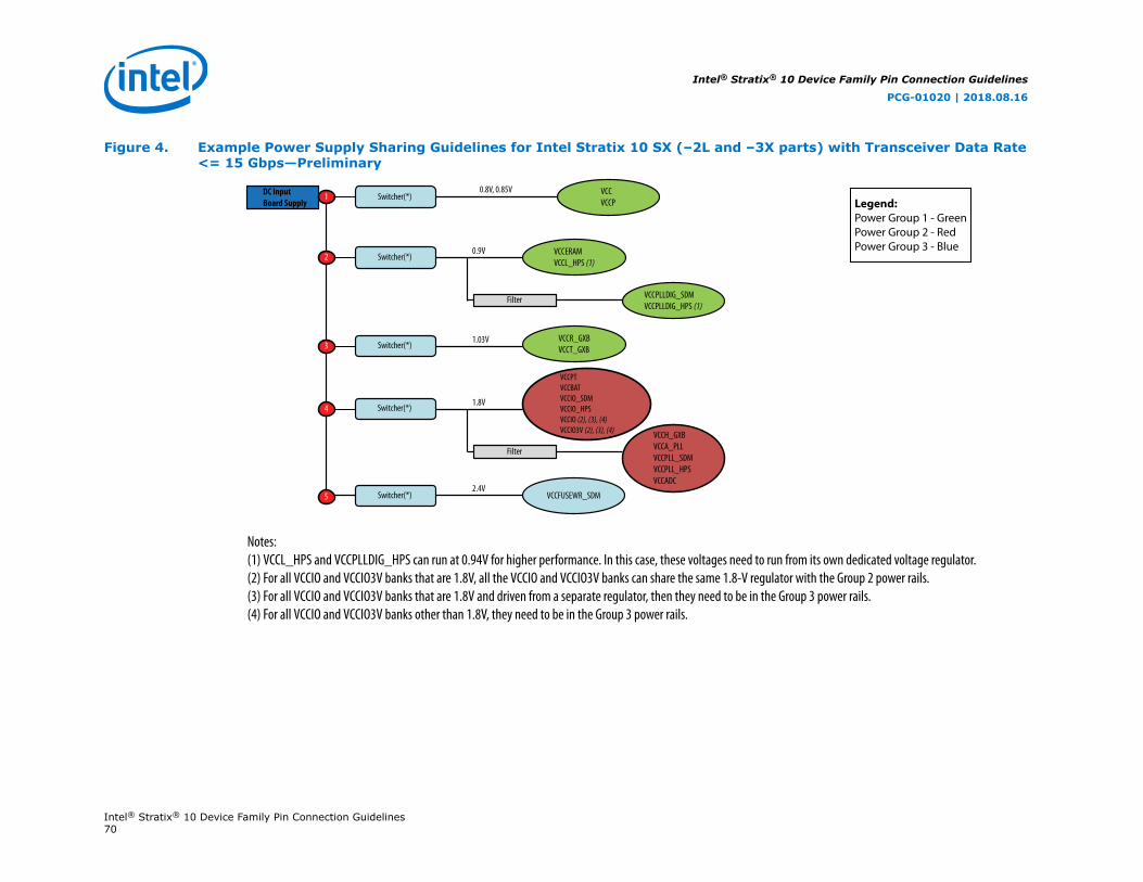
Figure 4. Example Power Supply Sharing Guidelines for Intel Stratix 10 SX (–2L and –3X parts) with Transceiver Data Rate<= 15 Gbps—Preliminary
0.8V, 0.85VDC InputBoard Supply
Switcher(*) VCCVCCP
1
0.9VSwitcher(*)
1.8VSwitcher(*)
VCCERAMVCCL_HPS (1)
VCCR_GXBVCCT_GXB
VCCPTVCCBATVCCIO_SDMVCCIO_HPSVCCIO (2), (3), (4)VCCIO3V (2), (3), (4)
2.4VSwitcher(*)
2
1.03V3
4
5 VCCFUSEWR_SDM
Filter VCCPLLDIG_SDMVCCPLLDIG_HPS (1)
VCCH_GXBVCCA_PLLVCCPLL_SDMVCCPLL_HPSVCCADC
Filter
Switcher(*)
Notes:(1) VCCL_HPS and VCCPLLDIG_HPS can run at 0.94V for higher performance. In this case, these voltages need to run from its own dedicated voltage regulator.(2) For all VCCIO and VCCIO3V banks that are 1.8V, all the VCCIO and VCCIO3V banks can share the same 1.8-V regulator with the Group 2 power rails. (3) For all VCCIO and VCCIO3V banks that are 1.8V and driven from a separate regulator, then they need to be in the Group 3 power rails.(4) For all VCCIO and VCCIO3V banks other than 1.8V, they need to be in the Group 3 power rails.
Legend:Power Group 1 - GreenPower Group 2 - RedPower Group 3 - Blue
Intel® Stratix® 10 Device Family Pin Connection Guidelines
PCG-01020 | 2018.08.16
Intel® Stratix® 10 Device Family Pin Connection Guidelines70

Example 5—Intel Stratix 10 SX (–1V, –2V, and –3V parts)
Table 34. Power Supply Sharing Guidelines for Intel Stratix 10 SX (–1V, –2V, and –3V parts) with 15 Gbps < TransceiverData Rate <= 28.3 Gbps—PreliminaryExample Requiring 6 Power Regulators
Power Pin Name Regulator Group Voltage Level (V) Supply Tolerance Power Source Regulator Sharing Notes
VCC 1 SmartVID ± 30mV Switcher (*) Share Source VCC and VCCP from the sameregulator, sharing the same voltageplane. You have the option to connectVCCL_HPS to the same regulator as VCCand VCCP when the power rails requirethe same voltage level. You may alsoconnect the VCCPLLDIG_HPS power tothe shared VCC, VCCP, and VCCL_HPSpower planes with proper isolationfiltering.When implementing a filtered supplytopology, you must consider the IR dropacross the filter.If you do not intend to utilize the HPS inthe Intel Stratix 10 SX device, you muststill provide power to the HPS powersupply. Do not leave the VCCL_HPS andVCCPLLDIG_HPS floating or connectthem to GND.
VCCP
VCCL_HPS
VCCPLLDIG_HPS Filter
VCCERAM 2 0.9 ± 30mV Switcher (*) Isolate Connect the VCCERAM to a dedicated0.9V power supply. You may connect theVCCPLLDIG_SDM power to the VCCERAMpower plane with proper isolationfiltering.When implementing a filtered supplytopology, you must consider the IR dropacross the filter.
VCCPLLDIG_SDM Filter
VCCR_GXB[L,R] 3 1.12 ± 20mV Switcher (*) Isolate Connect the VCCR_GXB to a dedicated1.12V power supply.
VCCT_GXB[L,R] 4 1.12 ± 20mV Switcher (*) Isolate Connect the VCCT_GXB to a dedicated1.12V power supply.
VCCPT 5 1.8 ± 5% (**) Switcher (*) Share if 1.8V You may source VCCPT and VCCIO_SDMfrom the same regulator. You mayconnect the VCCIO, VCCIO3V,VCCIO_SDM 1.8
continued...
Intel® Stratix® 10 Device Family Pin Connection Guidelines
PCG-01020 | 2018.08.16
Intel® Stratix® 10 Device Family Pin Connection Guidelines71

Power Pin Name Regulator Group Voltage Level (V) Supply Tolerance Power Source Regulator Sharing Notes
VCCIO VCCIO_HPS, and VCCBAT to the samepower plane if the those power rails areat the same voltage level. You may alsoconnect the VCCH_GXB, VCCA_PLL,VCCPLL_SDM, VCCPLL_HPS, and VCCADCto the same power plane with properisolation filtering. Depending on theregulator capabilities, you have theoption to share this supply with multipleIntel Stratix 10 devices.When implementing a filtered supplytopology, you must consider the IR dropacross the filter.If you do not intend to utilize the HPS inthe Intel Stratix 10 SX device, you muststill provide power to the HPS powersupply. Do not leave the VCCIO_HPS andVCCPLL_HPS floating or connect them toGND.
Varies
VCCIO3V Varies
VCCIO_HPS 1.8
VCCBAT Varies
VCCH_GXB[L,R] 1.8 Filter
VCCA_PLL 1.8
VCCPLL_SDM 1.8
VCCPLL_HPS 1.8
VCCADC 1.8
VCCFUSEWR_SDM 6 2.4 ± 50mV Switcher (*) Isolate Connect VCCFUSEWR_SDM to adedicated 2.4V power supply if the SDMfuses need to be written. LeaveVCCFUSEWR_SDM unconnected or tie itto VCCPT 1.8V power if the SDM fuses donot need to be written. Do not tie this pinto GND.
(*)When using a switcher to supply these voltages, the switcher must be a low noise switcher as defined as defined in note 6of the Notes to Intel Stratix 10 SX Pin Connection Guidelines.
(**)The supported tolerance for the VCCIO power supply varies depending on the I/O standards. For more details, refer tothe I/O standard specification in the Intel Stratix 10 Device Datasheet. Use the EPE (Early Power Estimator) and the IntelQuartus Prime Power Analyzer tool to assist in determining the power required for your specific design.
Each board design requires its own power analysis to determine the required power regulators needed to satisfy the specificboard design requirements. An example block diagram using the Intel Stratix 10 SX device is provided in Figure 5.
The voltage level for each power rail is preliminary.
Intel® Stratix® 10 Device Family Pin Connection Guidelines
PCG-01020 | 2018.08.16
Intel® Stratix® 10 Device Family Pin Connection Guidelines72

Figure 5. Example Power Supply Sharing Guidelines for Intel Stratix 10 SX (–1V, –2V, and –3V parts) with 15 Gbps <Transceiver Data Rate <= 28.3 Gbps—Preliminary
SmartVID (0.8V-0.94V)DC InputBoard Supply
Switcher(*)VCCVCCPVCCL_HPS (1)
1
0.9VSwitcher(*)
1.8VSwitcher(*)
VCCERAM
VCCR_GXB
VCCPTVCCBATVCCIO_SDMVCCIO_HPSVCCIO (2), (3), (4)VCCIO3V (2), (3), (4)
2.4VSwitcher(*)
2
1.12V3
5
6 VCCFUSEWR_SDM
Filter VCCPLLDIG_SDM
Filter VCCPLLDIG_HPS (1)
VCCH_GXBVCCA_PLLVCCPLL_SDMVCCPLL_HPSVCCADC
Filter
Switcher(*)
VCCT_GXB1.12V4 Switcher(*)
Notes:(1) VCCL_HPS and VCCPLLDIG_HPS can run at 0.94V for higher performance. In this case, these voltages need to run from its own dedicated voltage regulator.Optionally, you can connect VCCL_HPS and VCCPLLDIG_HPS to a fixed 0.9V. If you are connecting VCCL_HPS and VCCPLLDIG_HPS to 0.9V, they can share thesame power regulator with VCCERAM.(2) For all VCCIO and VCCIO3V banks that are 1.8V, all the VCCIO and VCCIO3V banks can share the same 1.8-V regulator with the Group 2 power rails. (3) For all VCCIO and VCCIO3V banks that are 1.8V and driven from a separate regulator, then they need to be in the Group 3 power rails.(4) For all VCCIO and VCCIO3V banks other than 1.8V, they need to be in the Group 3 power rails.(5) When a -V device is used, you must enable the SmartVID connection between the device and the VCC voltage regulator. For more information, refer to the connection guidelines of thePWRMGT_SCL, PWRMGT_SDA, and PWRMGT_ALERT pin function.
Legend:Power Group 1 - GreenPower Group 2 - RedPower Group 3 - Blue
Intel® Stratix® 10 Device Family Pin Connection Guidelines
PCG-01020 | 2018.08.16
Intel® Stratix® 10 Device Family Pin Connection Guidelines73

Example 6—Intel Stratix 10 SX (–2L and –3X parts)
Table 35. Power Supply Sharing Guidelines for Intel Stratix 10 SX (–2L and –3X parts) with 15 Gbps < Transceiver DataRate <= 28.3 Gbps—PreliminaryExample Requiring 6 Power Regulators
Power Pin Name Regulator Group Voltage Level (V) Supply Tolerance Power Source Regulator Sharing Notes
VCC 1 0.80.85
± 30mV Switcher (*) Share Source VCC and VCCP from the sameregulator, sharing the same voltageplane.When implementing a filtered supplytopology, you must consider the IR dropacross the filter.
VCCP
VCCERAM 2 0.9 ± 30mV Switcher (*) Share Connect the VCCERAM to a dedicated0.9V power supply. You have the optionto connect VCCL_HPS to the sameregulator as VCCERAM when the powerrails require the same voltage level. Youmay also connect the VCCPLLDIG_SDMand VCCPLLDIG_HPS power rails to theVCCERAM power plane with properisolation filtering.When implementing a filtered supplytopology, you must consider the IR dropacross the filter.If you do not intend to utilize the HPS inthe Intel Stratix 10 SX device, you muststill provide power to the HPS powersupply. Do not leave the VCCL_HPS andVCCPLLDIG_HPS floating or connectthem to GND.
VCCL_HPS
VCCPLLDIG_SDM Filter
VCCPLLDIG_HPS
VCCR_GXB[L,R] 3 1.12 ± 20mV Switcher (*) Isolate Connect the VCCR_GXB to a dedicated1.12V power supply.
VCCT_GXB[L,R] 4 1.12 ± 20mV Switcher (*) Isolate Connect the VCCT_GXB to a dedicated1.12V power supply.
VCCPT 5 1.8 ± 5% (**) Switcher (*) Share if 1.8V You may source VCCPT and VCCIO_SDMfrom the same regulator. You mayconnect the VCCIO, VCCIO3V,VCCIO_HPS, and VCCBAT to the samepower plane if the those power rails areat the same voltage level. You may also
VCCIO_SDM 1.8
VCCIO Varies
continued...
Intel® Stratix® 10 Device Family Pin Connection Guidelines
PCG-01020 | 2018.08.16
Intel® Stratix® 10 Device Family Pin Connection Guidelines74

Power Pin Name Regulator Group Voltage Level (V) Supply Tolerance Power Source Regulator Sharing Notes
VCCIO3V Varies connect the VCCH_GXB, VCCA_PLL,VCCPLL_SDM, VCCPLL_HPS, and VCCADCto the same power plane with properisolation filtering. Depending on theregulator capabilities, you have theoption to share this supply with multipleIntel Stratix 10 devices.When implementing a filtered supplytopology, you must consider the IR dropacross the filter.If you do not intend to utilize the HPS inthe Intel Stratix 10 SX device, you muststill provide power to the HPS powersupply. Do not leave the VCCIO_HPS andVCCPLL_HPS floating or connect them toGND.
VCCIO_HPS 1.8
VCCBAT Varies
VCCH_GXB[L,R] 1.8 Filter
VCCA_PLL 1.8
VCCPLL_SDM 1.8
VCCPLL_HPS 1.8
VCCADC 1.8
VCCFUSEWR_SDM 6 2.4 ± 50mV Switcher (*) Isolate Connect VCCFUSEWR_SDM to adedicated 2.4V power supply if the SDMfuses need to be written. LeaveVCCFUSEWR_SDM unconnected or tie itto VCCPT 1.8V power if the SDM fuses donot need to be written. Do not tie this pinto GND.
(*)When using a switcher to supply these voltages, the switcher must be a low noise switcher as defined as defined in note 6of the Notes to Intel Stratix 10 SX Pin Connection Guidelines.
(**)The supported tolerance for the VCCIO power supply varies depending on the I/O standards. For more details, refer tothe I/O standard specification in the Intel Stratix 10 Device Datasheet. Use the EPE (Early Power Estimator) and the IntelQuartus Prime Power Analyzer tool to assist in determining the power required for your specific design.
Each board design requires its own power analysis to determine the required power regulators needed to satisfy the specificboard design requirements. An example block diagram using the Intel Stratix 10 SX device is provided in Figure 6.
The voltage level for each power rail is preliminary.
Intel® Stratix® 10 Device Family Pin Connection Guidelines
PCG-01020 | 2018.08.16
Intel® Stratix® 10 Device Family Pin Connection Guidelines75

Figure 6. Example Power Supply Sharing Guidelines for Intel Stratix 10 SX (–2L and –3X parts) with 15 Gbps <Transceiver Data Rate <= 28.3 Gbps—Preliminary
0.8V, 0.85VDC InputBoard Supply
Switcher(*) VCCVCCP
1
0.9VSwitcher(*)
1.8VSwitcher(*)
VCCERAMVCCL_HPS (1)
VCCR_GXB
VCCPTVCCBATVCCIO_SDMVCCIO_HPSVCCIO (2), (3), (4)VCCIO3V (2), (3), (4)
2.4VSwitcher(*)
2
1.12V3
5
6 VCCFUSEWR_SDM
Filter VCCPLLDIG_SDMVCCPLLDIG_HPS (1)
VCCH_GXBVCCA_PLLVCCPLL_SDMVCCPLL_HPSVCCADC
Filter
Switcher(*)
VCCT_GXB1.12V4 Switcher(*)
Notes:(1) VCCL_HPS and VCCPLLDIG_HPS can run at 0.94V for higher performance. In this case, these voltages need to run from its own dedicated voltage regulator.(2) For all VCCIO and VCCIO3V banks that are 1.8V, all the VCCIO and VCCIO3V banks can share the same 1.8-V regulator with the Group 2 power rails. (3) For all VCCIO and VCCIO3V banks that are 1.8V and driven from a separate regulator, then they need to be in the Group 3 power rails.(4) For all VCCIO and VCCIO3V banks other than 1.8V, they need to be in the Group 3 power rails.
Legend:Power Group 1 - GreenPower Group 2 - RedPower Group 3 - Blue
Intel® Stratix® 10 Device Family Pin Connection Guidelines
PCG-01020 | 2018.08.16
Intel® Stratix® 10 Device Family Pin Connection Guidelines76

Example 7—Intel Stratix 10 MX (–1V, –2V, and –3V parts)
Table 36. Power Supply Sharing Guidelines for Intel Stratix 10 MX (–1V, –2V, and –3V parts) with Transceiver Data Rate<= 15 Gbps—PreliminaryExample Requiring 7 Power Regulators
Power Pin Name Regulator Group Voltage Level (V) Supply Tolerance Power Source Regulator Sharing Notes
VCC 1 SmartVID ± 30mV Switcher (*) Share Source VCC and VCCP from the sameregulator, sharing the same voltageplane. You have the option to connectVCCL_HPS to the same regulator as VCCand VCCP when the power rails requirethe same voltage level. You may alsoconnect the VCCPLLDIG_HPS power tothe shared VCC, VCCP, and VCCL_HPSpower planes with proper isolationfiltering.When implementing a filtered supplytopology, you must consider the IR dropacross the filter.If you do not intend to utilize the HPS inthe Intel Stratix 10 MX device, you muststill provide power to the HPS powersupply. Do not leave the VCCL_HPS andVCCPLLDIG_HPS floating or connectthem to GND.
VCCP
VCCL_HPS
VCCPLLDIG_HPS Filter
VCCERAM 2 0.9 ± 30mV Switcher (*) Isolate Connect the VCCERAM to a dedicated0.9V power supply. You may connect theVCCPLLDIG_SDM power to the VCCERAMpower plane with proper isolationfiltering.When implementing a filtered supplytopology, you must consider the IR dropacross the filter.
VCCPLLDIG_SDM Filter
VCCR_GXB[L,R] 3 1.03 ± 30mV Switcher (*) Share You have the option to source theVCCR_GXB and VCCT_GXB from thesame regulator when all the power railsrequire the same voltage level. For betterperformance and in order to meet PCIeGen 3 jitter specifications, isolateVCCR_GXB and VCCT_GXB from eachother with at least 30dB of isolation for a1MHz to 100MHz bandwidth.
VCCT_GXB[L,R]
continued...
Intel® Stratix® 10 Device Family Pin Connection Guidelines
PCG-01020 | 2018.08.16
Intel® Stratix® 10 Device Family Pin Connection Guidelines77

Power Pin Name Regulator Group Voltage Level (V) Supply Tolerance Power Source Regulator Sharing Notes
VCCPT 4 1.8 ± 5% (**) Switcher (*) Share if 1.8V You may source VCCPT and VCCIO_SDMfrom the same regulator. You mayconnect the VCCIO, VCCIO3V,VCCIO_HPS, and VCCBAT to the samepower plane if the those power rails areat the same voltage level. You may alsoconnect the VCCH_GXB, VCCA_PLL,VCCPLL_SDM, VCCPLL_HPS, and VCCADCto the same power plane with properisolation filtering. Depending on theregulator capabilities, you have theoption to share this supply with multipleIntel Stratix 10 devices.When implementing a filtered supplytopology, you must consider the IR dropacross the filter.
VCCIO_SDM 1.8
VCCIO Varies
VCCIO3V Varies
VCCIO_HPS 1.8
VCCBAT Varies
VCCH_GXB[L,R] 1.8 Filter
VCCA_PLL 1.8
VCCPLL_SDM 1.8
VCCPLL_HPS 1.8
VCCADC 1.8
VCCM_WORD_(BL,TL)
5 2.5 ± 100mV Switcher (*) Share Connect VCCM_WORD_(BL,TL) to a 2.5Vpower supply. You have the option toshare VCCM_WORD_(BL,TL) with other2.5V power supplies such as 2.5V VCCIO,if applicable.
VCCIO_UIB_(BL,TL)
6 1.2 ± 30mV Switcher (*) Isolate Connect VCCIO_UIB_(BL,TL) to a 1.2Vpower supply.
VCCFUSEWR_SDM 7 2.4 ± 50mV Switcher (*) Isolate Connect VCCFUSEWR_SDM to adedicated 2.4V power supply if the SDMfuses need to be written. LeaveVCCFUSEWR_SDM unconnected or tie itto VCCPT 1.8V power if the SDM fuses donot need to be written. Do not tie this pinto GND.
(*)When using a switcher to supply these voltages, the switcher must be a low noise switcher as defined as defined in note 7of the Notes to Intel Stratix 10 MX Pin Connection Guidelines.
(**)The supported tolerance for the VCCIO power supply varies depending on the I/O standards. For more details, refer tothe I/O standard specification in the Intel Stratix 10 Device Datasheet. Use the EPE (Early Power Estimator) and the IntelQuartus Prime Power Analyzer tool to assist in determining the power required for your specific design.
Intel® Stratix® 10 Device Family Pin Connection Guidelines
PCG-01020 | 2018.08.16
Intel® Stratix® 10 Device Family Pin Connection Guidelines78

Each board design requires its own power analysis to determine the required power regulators needed to satisfy the specificboard design requirements. An example block diagram using the Intel Stratix 10 MX device is provided in Figure 7.
The voltage level for each power rail is preliminary.
Intel® Stratix® 10 Device Family Pin Connection Guidelines
PCG-01020 | 2018.08.16
Intel® Stratix® 10 Device Family Pin Connection Guidelines79

Figure 7. Example Power Supply Sharing Guidelines for Intel Stratix 10 MX (–1V, –2V, and –3V parts) with TransceiverData Rate <= 15 Gbps—Preliminary
SmartVID (0.8V-0.94V)DC InputBoard Supply
Switcher(*)VCCVCCPVCCL_HPS (1)
1
0.9VSwitcher(*)
1.8VSwitcher(*)
VCCERAM
VCCR_GXBVCCT_GXB
VCCPTVCCBATVCCIO_SDMVCCIO_HPSVCCIO (2), (3), (4)VCCIO3V (2), (3), (4)
2
1.03V3
4
Filter VCCPLLDIG_SDM
Filter VCCPLLDIG_HPS (1)
2.5VSwitcher(*)5 VCCM_WORD_(BL,TL)
1.2VSwitcher(*)6
VCCFUSEWR_SDM2.4V
Switcher(*)7
VCCIO_UIB_(BL,TL)
VCCH_GXBVCCA_PLLVCCPLL_SDMVCCPLL_HPSVCCADC
Filter
Switcher(*)
Notes:(1) VCCL_HPS and VCCPLLDIG_HPS can run at 0.94V for higher performance. In this case, these voltages need to run from its own dedicated voltage regulator.Optionally, you can connect VCCL_HPS and VCCPLLDIG_HPS to a fixed 0.9V. If you are connecting VCCL_HPS and VCCPLLDIG_HPS to 0.9V, they can share thesame power regulator with VCCERAM.(2) For all VCCIO and VCCIO3V banks that are 1.8V, all the VCCIO and VCCIO3V banks can share the same 1.8-V regulator with the Group 2 power rails. (3) For all VCCIO and VCCIO3V banks that are 1.8V and driven from a separate regulator, then they need to be in the Group 3 power rails.(4) For all VCCIO and VCCIO3V banks other than 1.8V, they need to be in the Group 3 power rails.(5) When a -V device is used, you must enable the SmartVID connection between the device and the VCC voltage regulator. For more information, refer to the connection guidelines of thePWRMGT_SCL, PWRMGT_SDA, and PWRMGT_ALERT pin function.
Legend:Power Group 1 - GreenPower Group 2 - RedPower Group 3 - Blue
Intel® Stratix® 10 Device Family Pin Connection Guidelines
PCG-01020 | 2018.08.16
Intel® Stratix® 10 Device Family Pin Connection Guidelines80

Example 8—Intel Stratix 10 MX (–2L and –3X parts)
Table 37. Power Supply Sharing Guidelines for Intel Stratix 10 MX (–2L and –3X parts) with Transceiver Data Rate <= 15Gbps—PreliminaryExample Requiring 7 Power Regulators
Power Pin Name Regulator Group Voltage Level (V) Supply Tolerance Power Source Regulator Sharing Notes
VCC 1 0.80.85
± 30mV Switcher (*) Share Source VCC and VCCP from the sameregulator, sharing the same voltageplane.When implementing a filtered supplytopology, you must consider the IR dropacross the filter.
VCCP
VCCERAM 2 0.9 ± 30mV Switcher (*) Share Connect the VCCERAM to a dedicated0.9V power supply. You have the optionto connect VCCL_HPS to the sameregulator as VCCERAM when the powerrails require the same voltage level. Youmay also connect the VCCPLLDIG_SDMand VCCPLLDIG_HPS power rails to theVCCERAM power plane with properisolation filtering.When implementing a filtered supplytopology, you must consider the IR dropacross the filter.If you do not intend to utilize the HPS inthe Intel Stratix 10 MX device, you muststill provide power to the HPS powersupply. Do not leave the VCCL_HPS andVCCPLLDIG_HPS floating or connectthem to GND.
VCCL_HPS
VCCPLLDIG_SDM Filter
VCCPLLDIG_HPS
VCCR_GXB[L,R] 3 1.03 ± 30mV Switcher (*) Share You have the option to source theVCCR_GXB and VCCT_GXB from thesame regulator when all the power railsrequire the same voltage level. For betterperformance and in order to meet PCIeGen 3 jitter specifications, isolateVCCR_GXB and VCCT_GXB from eachother with at least 30dB of isolation for a1MHz to 100MHz bandwidth.
VCCT_GXB[L,R]
continued...
Intel® Stratix® 10 Device Family Pin Connection Guidelines
PCG-01020 | 2018.08.16
Intel® Stratix® 10 Device Family Pin Connection Guidelines81

Power Pin Name Regulator Group Voltage Level (V) Supply Tolerance Power Source Regulator Sharing Notes
VCCPT 4 1.8 ± 5% (**) Switcher (*) Share if 1.8V You may source VCCPT and VCCIO_SDMfrom the same regulator. You mayconnect the VCCIO, VCCIO3V,VCCIO_HPS, and VCCBAT to the samepower plane if the those power rails areat the same voltage level. You may alsoconnect the VCCH_GXB, VCCA_PLL,VCCPLL_SDM, VCCPLL_HPS, and VCCADCto the same power plane with properisolation filtering. Depending on theregulator capabilities, you have theoption to share this supply with multipleIntel Stratix 10 devices.When implementing a filtered supplytopology, you must consider the IR dropacross the filter.
VCCIO_SDM 1.8
VCCIO Varies
VCCIO3V Varies
VCCIO_HPS 1.8
VCCBAT Varies
VCCH_GXB[L,R] 1.8 Filter
VCCA_PLL 1.8
VCCPLL_SDM 1.8
VCCPLL_HPS 1.8
VCCADC 1.8
VCCM_WORD_(BL,TL)
5 2.5 ± 100mV Switcher (*) Share Connect VCCM_WORD_(BL,TL) to a 2.5Vpower supply. You have the option toshare VCCM_WORD_(BL,TL) with other2.5V power supplies such as 2.5V VCCIO,if applicable.
VCCIO_UIB_(BL,TL)
6 1.2 ± 30mV Switcher (*) Isolate Connect VCCIO_UIB_(BL,TL) to a 1.2Vpower supply.
VCCFUSEWR_SDM 7 2.4 ± 50mV Switcher (*) Isolate Connect VCCFUSEWR_SDM to adedicated 2.4V power supply if the SDMfuses need to be written. LeaveVCCFUSEWR_SDM unconnected or tie itto VCCPT 1.8V power if the SDM fuses donot need to be written. Do not tie this pinto GND.
(*)When using a switcher to supply these voltages, the switcher must be a low noise switcher as defined as defined in note 7of the Notes to Intel Stratix 10 MX Pin Connection Guidelines.
(**)The supported tolerance for the VCCIO power supply varies depending on the I/O standards. For more details, refer tothe I/O standard specification in the Intel Stratix 10 Device Datasheet. Use the EPE (Early Power Estimator) and the IntelQuartus Prime Power Analyzer tool to assist in determining the power required for your specific design.
Intel® Stratix® 10 Device Family Pin Connection Guidelines
PCG-01020 | 2018.08.16
Intel® Stratix® 10 Device Family Pin Connection Guidelines82

Each board design requires its own power analysis to determine the required power regulators needed to satisfy the specificboard design requirements. An example block diagram using the Intel Stratix 10 MX device is provided in Figure 8.
The voltage level for each power rail is preliminary.
Intel® Stratix® 10 Device Family Pin Connection Guidelines
PCG-01020 | 2018.08.16
Intel® Stratix® 10 Device Family Pin Connection Guidelines83

Figure 8. Example Power Supply Sharing Guidelines for Intel Stratix 10 MX (–2L and –3X parts) with Transceiver DataRate <= 15 Gbps—Preliminary
0.8V, 0.85VDC InputBoard Supply
Switcher(*) VCCVCCP
1
0.9VSwitcher(*)
1.8VSwitcher(*)
VCCERAMVCCL_HPS (1)
VCCR_GXBVCCT_GXB
VCCPTVCCBATVCCIO_SDMVCCIO_HPSVCCIO (2), (3), (4)VCCIO3V (2), (3), (4)
2
1.03V3
4
Filter VCCPLLDIG_SDMVCCPLLDIG_HPS (1)
2.5VSwitcher(*)5 VCCM_WORD_(BL,TL)
1.2VSwitcher(*)6
VCCFUSEWR_SDM2.4V
Switcher(*)7
VCCIO_UIB_(BL,TL)
VCCH_GXBVCCA_PLLVCCPLL_SDMVCCPLL_HPSVCCADC
Filter
Switcher(*)
Notes:(1) VCCL_HPS and VCCPLLDIG_HPS can run at 0.94V for higher performance. In this case, these voltages need to run from its own dedicated voltage regulator.(2) For all VCCIO and VCCIO3V banks that are 1.8V, all the VCCIO and VCCIO3V banks can share the same 1.8-V regulator with the Group 2 power rails. (3) For all VCCIO and VCCIO3V banks that are 1.8V and driven from a separate regulator, then they need to be in the Group 3 power rails.(4) For all VCCIO and VCCIO3V banks other than 1.8V, they need to be in the Group 3 power rails.
Legend:Power Group 1 - GreenPower Group 2 - RedPower Group 3 - Blue
Intel® Stratix® 10 Device Family Pin Connection Guidelines
PCG-01020 | 2018.08.16
Intel® Stratix® 10 Device Family Pin Connection Guidelines84

Example 9—Intel Stratix 10 MX (–1V, –2V, and –3V parts)
Table 38. Power Supply Sharing Guidelines for Intel Stratix 10 MX (–1V, –2V, and –3V parts) with 15 Gbps < TransceiverData Rate <= 28.3 Gbps—PreliminaryExample Requiring 8 Power Regulators
Power Pin Name Regulator Group Voltage Level (V) Supply Tolerance Power Source Regulator Sharing Notes
VCC 1 SmartVID ± 30mV Switcher (*) Share Source VCC and VCCP from the sameregulator, sharing the same voltageplane. You have the option to connectVCCL_HPS to the same regulator as VCCand VCCP when the power rails requirethe same voltage level. You may alsoconnect the VCCPLLDIG_HPS power tothe shared VCC, VCCP, and VCCL_HPSpower planes with proper isolationfiltering.When implementing a filtered supplytopology, you must consider the IR dropacross the filter.If you do not intend to utilize the HPS inthe Intel Stratix 10 MX device, you muststill provide power to the HPS powersupply. Do not leave the VCCL_HPS andVCCPLLDIG_HPS floating or connectthem to GND.
VCCP
VCCL_HPS
VCCPLLDIG_HPS Filter
VCCERAM 2 0.9 ± 30mV Switcher (*) Isolate Connect the VCCERAM to a dedicated0.9V power supply. You may connect theVCCPLLDIG_SDM power to the VCCERAMpower plane with proper isolationfiltering.When implementing a filtered supplytopology, you must consider the IR dropacross the filter.
VCCPLLDIG_SDM Filter
VCCR_GXB[L,R] 3 1.12 ± 20mV Switcher (*) Isolate Connect the VCCR_GXB to a dedicated1.12V power supply.
VCCT_GXB[L,R] 4 1.12 ± 20mV Switcher (*) Isolate Connect the VCCT_GXB to a dedicated1.12V power supply.
VCCPT 5 1.8 ± 5% (**) Switcher (*) Share if 1.8V You may source VCCPT and VCCIO_SDMfrom the same regulator. You mayconnect the VCCIO, VCCIO3V,VCCIO_SDM 1.8
continued...
Intel® Stratix® 10 Device Family Pin Connection Guidelines
PCG-01020 | 2018.08.16
Intel® Stratix® 10 Device Family Pin Connection Guidelines85
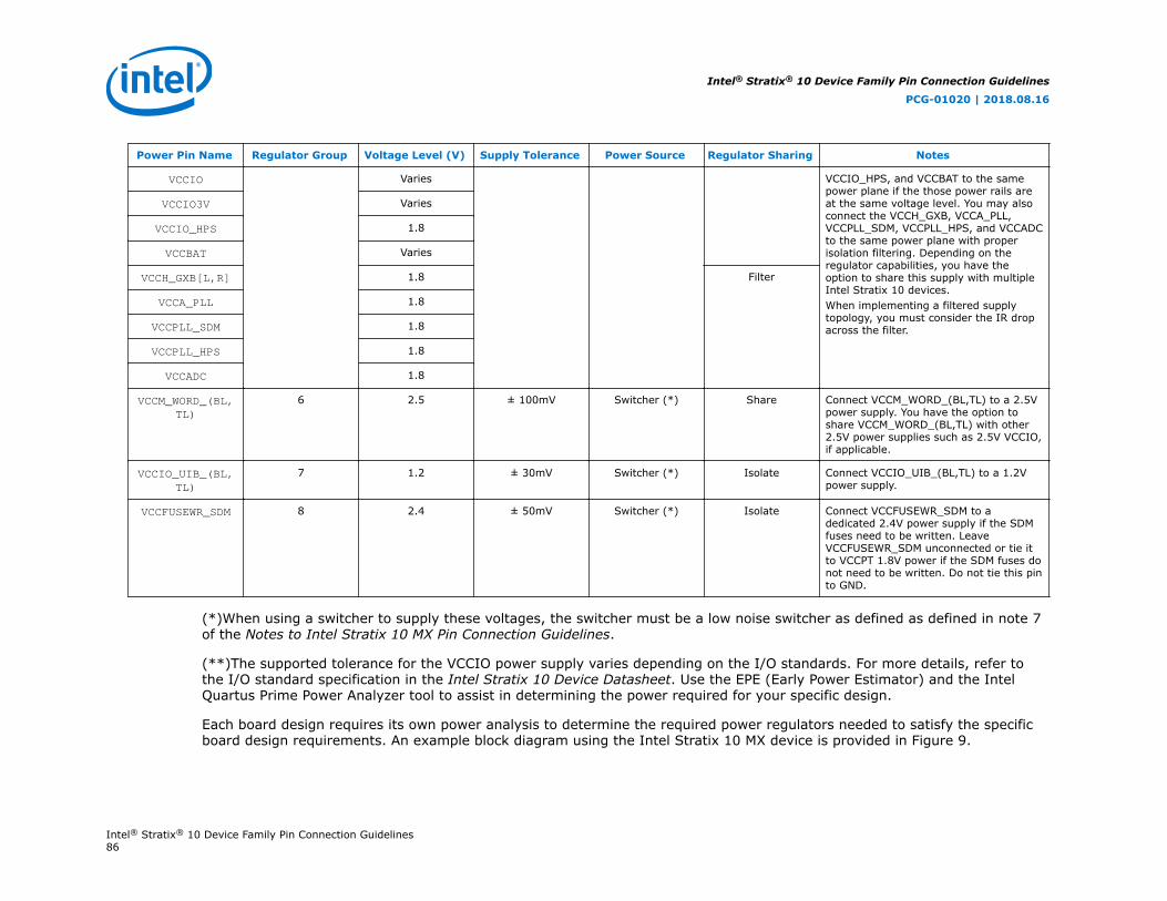
Power Pin Name Regulator Group Voltage Level (V) Supply Tolerance Power Source Regulator Sharing Notes
VCCIO VCCIO_HPS, and VCCBAT to the samepower plane if the those power rails areat the same voltage level. You may alsoconnect the VCCH_GXB, VCCA_PLL,VCCPLL_SDM, VCCPLL_HPS, and VCCADCto the same power plane with properisolation filtering. Depending on theregulator capabilities, you have theoption to share this supply with multipleIntel Stratix 10 devices.When implementing a filtered supplytopology, you must consider the IR dropacross the filter.
Varies
VCCIO3V Varies
VCCIO_HPS 1.8
VCCBAT Varies
VCCH_GXB[L,R] 1.8 Filter
VCCA_PLL 1.8
VCCPLL_SDM 1.8
VCCPLL_HPS 1.8
VCCADC 1.8
VCCM_WORD_(BL,TL)
6 2.5 ± 100mV Switcher (*) Share Connect VCCM_WORD_(BL,TL) to a 2.5Vpower supply. You have the option toshare VCCM_WORD_(BL,TL) with other2.5V power supplies such as 2.5V VCCIO,if applicable.
VCCIO_UIB_(BL,TL)
7 1.2 ± 30mV Switcher (*) Isolate Connect VCCIO_UIB_(BL,TL) to a 1.2Vpower supply.
VCCFUSEWR_SDM 8 2.4 ± 50mV Switcher (*) Isolate Connect VCCFUSEWR_SDM to adedicated 2.4V power supply if the SDMfuses need to be written. LeaveVCCFUSEWR_SDM unconnected or tie itto VCCPT 1.8V power if the SDM fuses donot need to be written. Do not tie this pinto GND.
(*)When using a switcher to supply these voltages, the switcher must be a low noise switcher as defined as defined in note 7of the Notes to Intel Stratix 10 MX Pin Connection Guidelines.
(**)The supported tolerance for the VCCIO power supply varies depending on the I/O standards. For more details, refer tothe I/O standard specification in the Intel Stratix 10 Device Datasheet. Use the EPE (Early Power Estimator) and the IntelQuartus Prime Power Analyzer tool to assist in determining the power required for your specific design.
Each board design requires its own power analysis to determine the required power regulators needed to satisfy the specificboard design requirements. An example block diagram using the Intel Stratix 10 MX device is provided in Figure 9.
Intel® Stratix® 10 Device Family Pin Connection Guidelines
PCG-01020 | 2018.08.16
Intel® Stratix® 10 Device Family Pin Connection Guidelines86

The voltage level for each power rail is preliminary.
Intel® Stratix® 10 Device Family Pin Connection Guidelines
PCG-01020 | 2018.08.16
Intel® Stratix® 10 Device Family Pin Connection Guidelines87

Figure 9. Example Power Supply Sharing Guidelines for Intel Stratix 10 MX (–1V, –2V, and –3V parts) with 15 Gbps <Transceiver Data Rate <= 28.3 Gbps—Preliminary
SmartVID (0.8V-0.94V)DC InputBoard Supply
Switcher(*)VCCVCCPVCCL_HPS (1)
1
0.9VSwitcher(*)
1.8VSwitcher(*)
VCCERAM
VCCR_GXB
VCCPTVCCBATVCCIO_SDMVCCIO_HPSVCCIO (2), (3), (4)VCCIO3V (2), (3), (4)
2
1.12V3
5
Filter VCCPLLDIG_SDM
Filter VCCPLLDIG_HPS (1)
2.5VSwitcher(*)6 VCCM_WORD_(BL,TL)
1.2VSwitcher(*)7
2.4VSwitcher(*)8
VCCIO_UIB_(BL,TL)
VCCH_GXBVCCA_PLLVCCPLL_SDMVCCPLL_HPSVCCADC
Filter
Switcher(*)
VCCT_GXB1.12V4 Switcher(*)
Notes:(1) VCCL_HPS and VCCPLLDIG_HPS can run at 0.94V for higher performance. In this case, these voltages need to run from its own dedicated voltage regulator.Optionally, you can connect VCCL_HPS and VCCPLLDIG_HPS to a fixed 0.9V. If you are connecting VCCL_HPS and VCCPLLDIG_HPS to 0.9V, they can share thesame power regulator with VCCERAM.(2) For all VCCIO and VCCIO3V banks that are 1.8V, all the VCCIO and VCCIO3V banks can share the same 1.8-V regulator with the Group 2 power rails. (3) For all VCCIO and VCCIO3V banks that are 1.8V and driven from a separate regulator, then they need to be in the Group 3 power rails.(4) For all VCCIO and VCCIO3V banks other than 1.8V, they need to be in the Group 3 power rails.(5) When a -V device is used, you must enable the SmartVID connection between the device and the VCC voltage regulator. For more information, refer to the connection guidelines of the PWRMGT_SCL, PWRMGT_SDA, and PWRMGT_ALERT pin function.
VCCFUSEWR_SDM
Legend:Power Group 1 - GreenPower Group 2 - RedPower Group 3 - Blue
Intel® Stratix® 10 Device Family Pin Connection Guidelines
PCG-01020 | 2018.08.16
Intel® Stratix® 10 Device Family Pin Connection Guidelines88
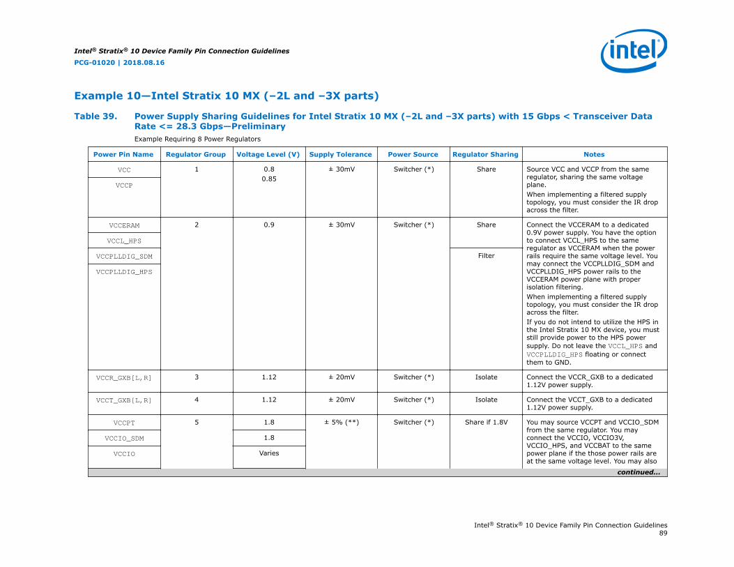
Example 10—Intel Stratix 10 MX (–2L and –3X parts)
Table 39. Power Supply Sharing Guidelines for Intel Stratix 10 MX (–2L and –3X parts) with 15 Gbps < Transceiver DataRate <= 28.3 Gbps—PreliminaryExample Requiring 8 Power Regulators
Power Pin Name Regulator Group Voltage Level (V) Supply Tolerance Power Source Regulator Sharing Notes
VCC 1 0.80.85
± 30mV Switcher (*) Share Source VCC and VCCP from the sameregulator, sharing the same voltageplane.When implementing a filtered supplytopology, you must consider the IR dropacross the filter.
VCCP
VCCERAM 2 0.9 ± 30mV Switcher (*) Share Connect the VCCERAM to a dedicated0.9V power supply. You have the optionto connect VCCL_HPS to the sameregulator as VCCERAM when the powerrails require the same voltage level. Youmay connect the VCCPLLDIG_SDM andVCCPLLDIG_HPS power rails to theVCCERAM power plane with properisolation filtering.When implementing a filtered supplytopology, you must consider the IR dropacross the filter.If you do not intend to utilize the HPS inthe Intel Stratix 10 MX device, you muststill provide power to the HPS powersupply. Do not leave the VCCL_HPS andVCCPLLDIG_HPS floating or connectthem to GND.
VCCL_HPS
VCCPLLDIG_SDM Filter
VCCPLLDIG_HPS
VCCR_GXB[L,R] 3 1.12 ± 20mV Switcher (*) Isolate Connect the VCCR_GXB to a dedicated1.12V power supply.
VCCT_GXB[L,R] 4 1.12 ± 20mV Switcher (*) Isolate Connect the VCCT_GXB to a dedicated1.12V power supply.
VCCPT 5 1.8 ± 5% (**) Switcher (*) Share if 1.8V You may source VCCPT and VCCIO_SDMfrom the same regulator. You mayconnect the VCCIO, VCCIO3V,VCCIO_HPS, and VCCBAT to the samepower plane if the those power rails areat the same voltage level. You may also
VCCIO_SDM 1.8
VCCIO Varies
continued...
Intel® Stratix® 10 Device Family Pin Connection Guidelines
PCG-01020 | 2018.08.16
Intel® Stratix® 10 Device Family Pin Connection Guidelines89
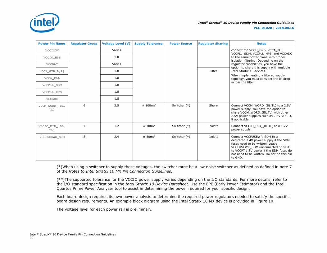
Power Pin Name Regulator Group Voltage Level (V) Supply Tolerance Power Source Regulator Sharing Notes
VCCIO3V Varies connect the VCCH_GXB, VCCA_PLL,VCCPLL_SDM, VCCPLL_HPS, and VCCADCto the same power plane with properisolation filtering. Depending on theregulator capabilities, you have theoption to share this supply with multipleIntel Stratix 10 devices.When implementing a filtered supplytopology, you must consider the IR dropacross the filter.
VCCIO_HPS 1.8
VCCBAT Varies
VCCH_GXB[L,R] 1.8 Filter
VCCA_PLL 1.8
VCCPLL_SDM 1.8
VCCPLL_HPS 1.8
VCCADC 1.8
VCCM_WORD_(BL,TL)
6 2.5 ± 100mV Switcher (*) Share Connect VCCM_WORD_(BL,TL) to a 2.5Vpower supply. You have the option toshare VCCM_WORD_(BL,TL) with other2.5V power supplies such as 2.5V VCCIO,if applicable.
VCCIO_UIB_(BL,TL)
7 1.2 ± 30mV Switcher (*) Isolate Connect VCCIO_UIB_(BL,TL) to a 1.2Vpower supply.
VCCFUSEWR_SDM 8 2.4 ± 50mV Switcher (*) Isolate Connect VCCFUSEWR_SDM to adedicated 2.4V power supply if the SDMfuses need to be written. LeaveVCCFUSEWR_SDM unconnected or tie itto VCCPT 1.8V power if the SDM fuses donot need to be written. Do not tie this pinto GND.
(*)When using a switcher to supply these voltages, the switcher must be a low noise switcher as defined as defined in note 7of the Notes to Intel Stratix 10 MX Pin Connection Guidelines.
(**)The supported tolerance for the VCCIO power supply varies depending on the I/O standards. For more details, refer tothe I/O standard specification in the Intel Stratix 10 Device Datasheet. Use the EPE (Early Power Estimator) and the IntelQuartus Prime Power Analyzer tool to assist in determining the power required for your specific design.
Each board design requires its own power analysis to determine the required power regulators needed to satisfy the specificboard design requirements. An example block diagram using the Intel Stratix 10 MX device is provided in Figure 10.
The voltage level for each power rail is preliminary.
Intel® Stratix® 10 Device Family Pin Connection Guidelines
PCG-01020 | 2018.08.16
Intel® Stratix® 10 Device Family Pin Connection Guidelines90

Figure 10. Example Power Supply Sharing Guidelines for Intel Stratix 10 MX (–2L and –3X parts) with 15 Gbps <Transceiver Data Rate <= 28.3 Gbps—Preliminary
0.8V, 0.85VDC InputBoard Supply
Switcher(*)VCCVCCP
1
0.9VSwitcher(*)
1.8VSwitcher(*)
VCCERAMVCCL_HPS (1)
VCCR_GXB
VCCPTVCCBATVCCIO_SDMVCCIO_HPSVCCIO (2), (3), (4)VCCIO3V (2), (3), (4)
2
1.12V3
5
Filter VCCPLLDIG_SDMVCCPLLDIG_HPS (1)
2.5VSwitcher(*)6 VCCM_WORD_(BL,TL)
1.2VSwitcher(*)7
2.4VSwitcher(*)8
VCCIO_UIB_(BL,TL)
VCCH_GXBVCCA_PLLVCCPLL_SDMVCCPLL_HPSVCCADC
Filter
Switcher(*)
VCCT_GXB1.12V4 Switcher(*)
Notes:(1) VCCL_HPS and VCCPLLDIG_HPS can run at 0.94V for higher performance. In this case, these voltages need to run from its own dedicated voltage regulator.(2) For all VCCIO and VCCIO3V banks that are 1.8V, all the VCCIO and VCCIO3V banks can share the same 1.8-V regulator with the Group 2 power rails. (3) For all VCCIO and VCCIO3V banks that are 1.8V and driven from a separate regulator, then they need to be in the Group 3 power rails.(4) For all VCCIO and VCCIO3V banks other than 1.8V, they need to be in the Group 3 power rails.
VCCFUSEWR_SDM
Legend:Power Group 1 - GreenPower Group 2 - RedPower Group 3 - Blue
Intel® Stratix® 10 Device Family Pin Connection Guidelines
PCG-01020 | 2018.08.16
Intel® Stratix® 10 Device Family Pin Connection Guidelines91

Example 11—Intel Stratix 10 TX (–1V, –2V, and –3V parts)
Table 40. Power Supply Sharing Guidelines for Intel Stratix 10 TX (–1V, –2V, and –3V parts) with 10 Gbps < TransceiverData Rate <= 57.8 Gbps—PreliminaryExample Requiring 11 Power Regulators
Power Pin Name Regulator Group Voltage Level (V) Supply Tolerance Power Source Regulator Sharing Notes
VCC 1 SmartVID ± 30mV Switcher (*) Share Source VCC and VCCP from the sameregulator, sharing the same voltageplane. You have the option to connectVCCL_HPS to the same regulator as VCCand VCCP when the power rails requirethe same voltage level. You may alsoconnect the VCCPLLDIG_HPS power tothe shared VCC, VCCP, and VCCL_HPSpower planes with proper isolationfiltering.When implementing a filtered supplytopology, you must consider the IR dropacross the filter.If you do not intend to utilize the HPS inthe Intel Stratix 10 TX device, you muststill provide power to the HPS powersupply. Do not leave the VCCL_HPS andVCCPLLDIG_HPS floating or connectthem to GND.
VCCP
VCCL_HPS
VCCPLLDIG_HPS Filter
VCCERAM 2 0.9 ± 30mV Switcher (*) Isolate Connect the VCCERAM to a dedicated0.9V power supply. You may connect theVCCPLLDIG_SDM power to the VCCERAMpower plane with proper isolationfiltering.When implementing a filtered supplytopology, you must consider the IR dropacross the filter.
VCCPLLDIG_SDM Filter
VCCR_GXB[L,R] 3 1.12 ± 20mV Switcher (*) Isolate Connect the VCCR_GXB to a dedicated1.12V power supply.
VCCT_GXB[L,R] 4 1.12 ± 20mV Switcher (*) Isolate Connect the VCCT_GXB to a dedicated1.12V power supply.
VCCRT_GXE 5 0.9 ± 5% (**) Switcher (*) Share Connect the VCCRT_GXE to a dedicated0.9V power supply.
continued...
Intel® Stratix® 10 Device Family Pin Connection Guidelines
PCG-01020 | 2018.08.16
Intel® Stratix® 10 Device Family Pin Connection Guidelines92
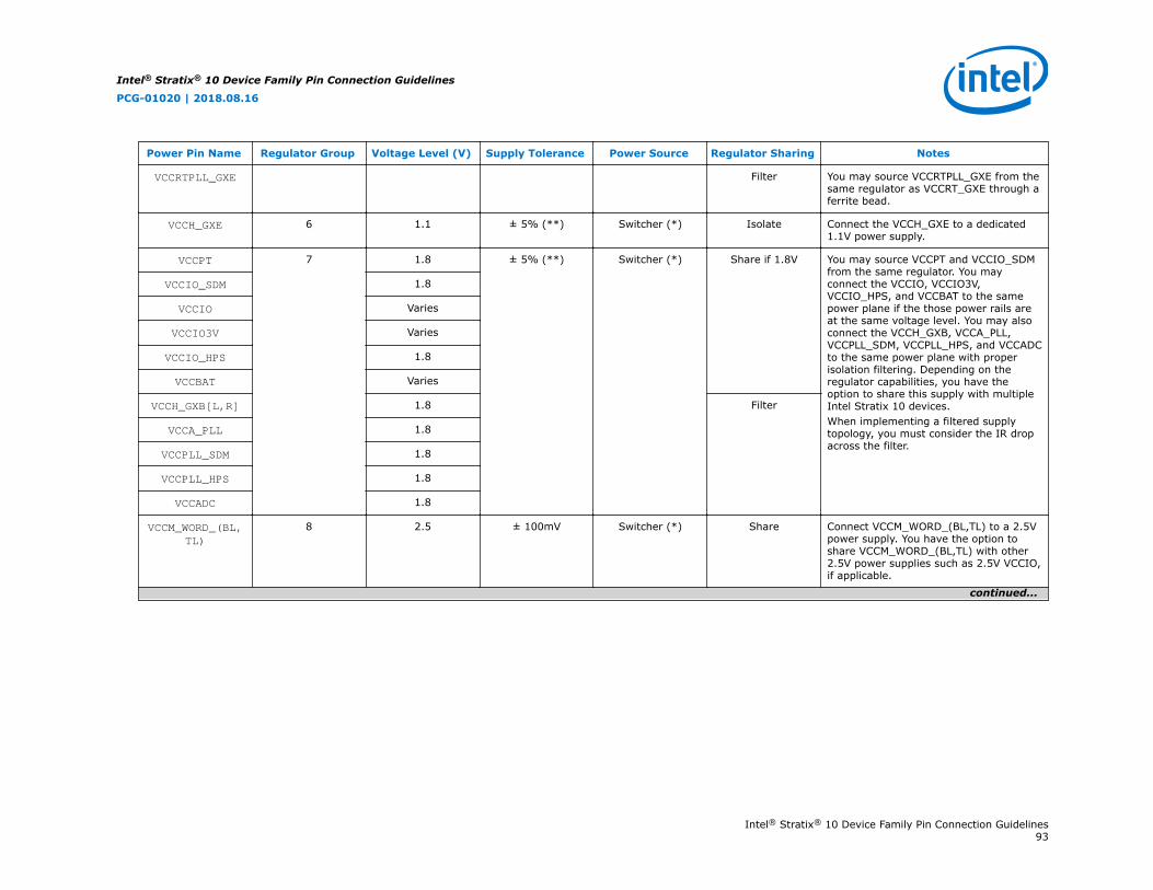
Power Pin Name Regulator Group Voltage Level (V) Supply Tolerance Power Source Regulator Sharing Notes
VCCRTPLL_GXE Filter You may source VCCRTPLL_GXE from thesame regulator as VCCRT_GXE through aferrite bead.
VCCH_GXE 6 1.1 ± 5% (**) Switcher (*) Isolate Connect the VCCH_GXE to a dedicated1.1V power supply.
VCCPT 7 1.8 ± 5% (**) Switcher (*) Share if 1.8V You may source VCCPT and VCCIO_SDMfrom the same regulator. You mayconnect the VCCIO, VCCIO3V,VCCIO_HPS, and VCCBAT to the samepower plane if the those power rails areat the same voltage level. You may alsoconnect the VCCH_GXB, VCCA_PLL,VCCPLL_SDM, VCCPLL_HPS, and VCCADCto the same power plane with properisolation filtering. Depending on theregulator capabilities, you have theoption to share this supply with multipleIntel Stratix 10 devices.When implementing a filtered supplytopology, you must consider the IR dropacross the filter.
VCCIO_SDM 1.8
VCCIO Varies
VCCIO3V Varies
VCCIO_HPS 1.8
VCCBAT Varies
VCCH_GXB[L,R] 1.8 Filter
VCCA_PLL 1.8
VCCPLL_SDM 1.8
VCCPLL_HPS 1.8
VCCADC 1.8
VCCM_WORD_(BL,TL)
8 2.5 ± 100mV Switcher (*) Share Connect VCCM_WORD_(BL,TL) to a 2.5Vpower supply. You have the option toshare VCCM_WORD_(BL,TL) with other2.5V power supplies such as 2.5V VCCIO,if applicable.
continued...
Intel® Stratix® 10 Device Family Pin Connection Guidelines
PCG-01020 | 2018.08.16
Intel® Stratix® 10 Device Family Pin Connection Guidelines93

Power Pin Name Regulator Group Voltage Level (V) Supply Tolerance Power Source Regulator Sharing Notes
VCCIO_UIB_(BL,TL)
9 1.2 ± 30mV Switcher (*) Isolate Connect VCCIO_UIB_(BL,TL) to a 1.2Vpower supply.
VCCCLK_GXE 10 2.5 ± 5% (**) Switcher (*) Isolate Connect VCCCLK_GXE to a dedicated2.5V power supply.
VCCFUSEWR_SDM 11 2.4 ± 50mV Switcher (*) Isolate Connect VCCFUSEWR_SDM to adedicated 2.4V power supply if the SDMfuses need to be written. LeaveVCCFUSEWR_SDM unconnected or tie itto VCCPT 1.8V power if the SDM fuses donot need to be written. Do not tie this pinto GND.
(*)When using a switcher to supply these voltages, the switcher must be a low noise switcher as defined as defined in note 7of the Notes to Intel Stratix 10 TX Pin Connection Guidelines.
(**)The supported tolerance for the VCCIO power supply varies depending on the I/O standards. For more details, refer tothe I/O standard specification in the Intel Stratix 10 Device Datasheet. Use the EPE (Early Power Estimator) and the IntelQuartus Prime Power Analyzer tool to assist in determining the power required for your specific design.
Each board design requires its own power analysis to determine the required power regulators needed to satisfy the specificboard design requirements. An example block diagram using the Intel Stratix 10 TX device is provided in Figure 11.
The voltage level for each power rail is preliminary.
Intel® Stratix® 10 Device Family Pin Connection Guidelines
PCG-01020 | 2018.08.16
Intel® Stratix® 10 Device Family Pin Connection Guidelines94

Figure 11. Example Power Supply Sharing Guidelines for Intel Stratix 10 TX (–1V, –2V, and –3V parts) with 10 Gbps <Transceiver Data Rate <= 57.8 Gbps—Preliminary
SmartVID (0.8V-0.94V)DC InputBoard Supply
Switcher(*)VCCVCCPVCCL_HPS (1)
1
1.8VSwitcher(*)
VCCR_GXB
VCCPTVCCBATVCCIO_SDMVCCIO_HPSVCCIO (2), (3), (4)VCCIO3V (2), (3), (4)
1.12V3
7
0.9VSwitcher(*) VCCRT_GXE
VCCRTPLL_GXE
5
Filter
0.9VSwitcher(*) VCCERAM2
Filter VCCPLLDIG_SDM
Filter VCCPLLDIG_HPS (1)
2.5VSwitcher(*)8 VCCM_WORD_(BL,TL)
1.1VSwitcher(*)6 VCCH_GXE
1.2VSwitcher(*)9 VCCIO_UIB_(BL,TL)
2.4VSwitcher(*)11 VCCFUSEWR_SDM
2.5VSwitcher(*)10 VCCCLK_GXE
VCCH_GXBVCCA_PLLVCCPLL_SDMVCCPLL_HPSVCCADC
Filter
Switcher(*)
VCCT_GXB1.12V4 Switcher(*)
Notes:(1) VCCL_HPS and VCCPLLDIG_HPS can run at 0.94V for higher performance. In this case, these voltages need to run from its own dedicated voltage regulator.Optionally, you can connect VCCL_HPS and VCCPLLDIG_HPS to a fixed 0.9V. If you are connecting VCCL_HPS and VCCPLLDIG_HPS to 0.9V, they can share thesame power regulator with VCCERAM.(2) For all VCCIO and VCCIO3V banks that are 1.8V, all the VCCIO and VCCIO3V banks can share the same 1.8-V regulator with the Group 2 power rails. (3) For all VCCIO and VCCIO3V banks that are 1.8V and driven from a separate regulator, then they need to be in the Group 3 power rails.(4) For all VCCIO and VCCIO3V banks other than 1.8V, they need to be in the Group 3 power rails.(5) When a -V device is used, you must enable the SmartVID connection between the device and the VCC voltage regulator. For more information, refer to the connection guidelines of the PWRMGT_SCL, PWRMGT_SDA, and PWRMGT_ALERT pin function.
Legend:Power Group 1 - GreenPower Group 2 - RedPower Group 3 - Blue
Intel® Stratix® 10 Device Family Pin Connection Guidelines
PCG-01020 | 2018.08.16
Intel® Stratix® 10 Device Family Pin Connection Guidelines95

Example 12—Intel Stratix 10 TX (–2L and –3X parts)
Table 41. Power Supply Sharing Guidelines for Intel Stratix 10 TX (–2L and –3X parts) with 10 Gbps < Transceiver DataRate <= 57.8 Gbps—PreliminaryExample Requiring 11 Power Regulators
Power Pin Name Regulator Group Voltage Level (V) Supply Tolerance Power Source Regulator Sharing Notes
VCC 1 0.80.85
± 30mV Switcher (*) Share Source VCC and VCCP from the sameregulator, sharing the same voltageplane.When implementing a filtered supplytopology, you must consider the IR dropacross the filter.
VCCP
VCCERAM 2 0.9 ± 30mV Switcher (*) Share Connect the VCCERAM to a dedicated0.9V power supply. You have the optionto connect VCCL_HPS to the sameregulator as VCCERAM when the powerrails require the same voltage level. Youmay connect the VCCPLLDIG_SDM andVCCPLLDIG_HPS power rails to theVCCERAM power plane with properisolation filtering.When implementing a filtered supplytopology, you must consider the IR dropacross the filter.If you do not intend to utilize the HPS inthe Intel Stratix 10 TX device, you muststill provide power to the HPS powersupply. Do not leave the VCCL_HPS andVCCPLLDIG_HPS floating or connectthem to GND.
VCCL_HPS
VCCPLLDIG_SDM Filter
VCCPLLDIG_HPS
VCCR_GXB[L,R] 3 1.12 ± 20mV Switcher (*) Isolate Connect the VCCR_GXB to a dedicated1.12V power supply.
VCCT_GXB[L,R] 4 1.12 ± 20mV Switcher (*) Isolate Connect the VCCT_GXB to a dedicated1.12V power supply.
VCCRT_GXE 5 0.9 ± 5% (**) Switcher (*) Share Connect the VCCRT_GXE to a dedicated0.9V power supply.
VCCRTPLL_GXE Filter You may source VCCRTPLL_GXE from thesame regulator as VCCRT_GXE through aferrite bead.
continued...
Intel® Stratix® 10 Device Family Pin Connection Guidelines
PCG-01020 | 2018.08.16
Intel® Stratix® 10 Device Family Pin Connection Guidelines96

Power Pin Name Regulator Group Voltage Level (V) Supply Tolerance Power Source Regulator Sharing Notes
VCCH_GXE 6 1.1 ± 5% (**) Switcher (*) Isolate Connect the VCCH_GXE to a dedicated1.1V power supply.
VCCPT 7 1.8 ± 5% (**) Switcher (*) Share if 1.8V You may source VCCPT and VCCIO_SDMfrom the same regulator. You mayconnect the VCCIO, VCCIO3V,VCCIO_HPS, and VCCBAT to the samepower plane if the those power rails areat the same voltage level. You may alsoconnect the VCCH_GXB, VCCA_PLL,VCCPLL_SDM, VCCPLL_HPS, and VCCADCto the same power plane with properisolation filtering. Depending on theregulator capabilities, you have theoption to share this supply with multipleIntel Stratix 10 devices.When implementing a filtered supplytopology, you must consider the IR dropacross the filter.
VCCIO_SDM 1.8
VCCIO Varies
VCCIO3V Varies
VCCIO_HPS 1.8
VCCBAT Varies
VCCH_GXB[L,R] 1.8 Filter
VCCA_PLL 1.8
VCCPLL_SDM 1.8
VCCPLL_HPS 1.8
VCCADC 1.8
VCCM_WORD_(BL,TL)
8 2.5 ± 100mV Switcher (*) Share Connect VCCM_WORD_(BL,TL) to a 2.5Vpower supply. You have the option toshare VCCM_WORD_(BL,TL) with other2.5V power supplies such as 2.5V VCCIO,if applicable.
VCCIO_UIB_(BL,TL)
9 1.2 ± 30mV Switcher (*) Isolate Connect VCCIO_UIB_(BL,TL) to a 1.2Vpower supply.
VCCCLK_GXE 10 2.5 ± 5% (**) Switcher (*) Isolate Connect VCCCLK_GXE to a dedicated2.5V power supply.
VCCFUSEWR_SDM 11 2.4 ± 50mV Switcher (*) Isolate Connect VCCFUSEWR_SDM to adedicated 2.4V power supply if the SDMfuses need to be written. LeaveVCCFUSEWR_SDM unconnected or tie itto VCCPT 1.8V power if the SDM fuses donot need to be written. Do not tie this pinto GND.
(*)When using a switcher to supply these voltages, the switcher must be a low noise switcher as defined as defined in note 7of the Notes to Intel Stratix 10 TX Pin Connection Guidelines.
Intel® Stratix® 10 Device Family Pin Connection Guidelines
PCG-01020 | 2018.08.16
Intel® Stratix® 10 Device Family Pin Connection Guidelines97

(**)The supported tolerance for the VCCIO power supply varies depending on the I/O standards. For more details, refer tothe I/O standard specification in the Intel Stratix 10 Device Datasheet. Use the EPE (Early Power Estimator) and the IntelQuartus Prime Power Analyzer tool to assist in determining the power required for your specific design.
Each board design requires its own power analysis to determine the required power regulators needed to satisfy the specificboard design requirements. An example block diagram using the Intel Stratix 10 TX device is provided in Figure 12.
The voltage level for each power rail is preliminary.
Intel® Stratix® 10 Device Family Pin Connection Guidelines
PCG-01020 | 2018.08.16
Intel® Stratix® 10 Device Family Pin Connection Guidelines98

Figure 12. Example Power Supply Sharing Guidelines for Intel Stratix 10 TX (–2L and –3X parts) with 10 Gbps <Transceiver Data Rate <= 57.8 Gbps—Preliminary
0.8V, 0.85VDC InputBoard Supply
Switcher(*)VCCVCCP
1
1.8VSwitcher(*)
VCCR_GXB
VCCPTVCCBATVCCIO_SDMVCCIO_HPSVCCIO (2), (3), (4)VCCIO3V (2), (3), (4)
1.12V3
7
0.9VSwitcher(*) VCCRT_GXE
VCCRTPLL_GXE
5
Filter
0.9VSwitcher(*)
VCCERAMVCCL_HPS (1)
2
Filter VCCPLLDIG_SDMVCCPLLDIG_HPS (1)
2.5VSwitcher(*)8 VCCM_WORD_(BL,TL)
1.1VSwitcher(*)6 VCCH_GXE
1.2VSwitcher(*)9 VCCIO_UIB_(BL,TL)
2.4VSwitcher(*)11 VCCFUSEWR_SDM
2.5VSwitcher(*)10 VCCCLK_GXE
VCCH_GXBVCCA_PLLVCCPLL_SDMVCCPLL_HPSVCCADC
Filter
Switcher(*)
VCCT_GXB1.12V4 Switcher(*)
Notes:(1) VCCL_HPS and VCCPLLDIG_HPS can run at 0.94V for higher performance. In this case, these voltages need to run from its own dedicated voltage regulator.(2) For all VCCIO and VCCIO3V banks that are 1.8V, all the VCCIO and VCCIO3V banks can share the same 1.8-V regulator with the Group 2 power rails. (3) For all VCCIO and VCCIO3V banks that are 1.8V and driven from a separate regulator, then they need to be in the Group 3 power rails.(4) For all VCCIO and VCCIO3V banks other than 1.8V, they need to be in the Group 3 power rails.
Legend:Power Group 1 - GreenPower Group 2 - RedPower Group 3 - Blue
Intel® Stratix® 10 Device Family Pin Connection Guidelines
PCG-01020 | 2018.08.16
Intel® Stratix® 10 Device Family Pin Connection Guidelines99

Document Revision History for the Intel Stratix 10 Device Family Pin Connection Guidelines
DocumentVersion
Changes
2018.08.16 • Added description that these pins can be used for the HPS in the TCK, TMS, TDO, TDI, JTAG_TCK, JTAG_TMS, JTAG_TDO, and JTAG_TDI pins.• Added note 13 to the Notes to Intel Stratix 10 GX Pin Connection Guidelines section.• Added the HPS_COLD_nRESET function to SDM_IO0, SDM_IO10, SDM_IO11, SDM_IO12, SDM_IO13, SDM_IO14, SDM_IO15, and SDM_IO16 pins.• Added a description to Transceiver Pins section for reference to the nPERST[L,R][0:2] pins.• Added the PWRMGT_ALERT pin function in the SDM_IO0 and SDM_IO12 pins.• Updated the connection guidelines of the VCCR_GXB[L1,R4] [C,D,E,F,G,H,I,J,K,L,M,N] and VCCT_GXB[L1,R4]
[C,D,E,F,G,H,I,J,K,L,M,N] pins.• Updated the VCCH_GXB[L,R] pin name to VCCH_GXB[L1,R4][C,D,E,F,G,H,I,J,K,L,M,N].• Updated the connection guidelines for the GXB[L1,R4][C,D,E,F,G,H,I,J,K,L,M,N]_RX_CH[0:5]p, GXB[L1,R4]
[C,D,E,F,G,H,I,J,K,L,M,N]_REFCLK[0:5]p, GXB[L1,R4][C,D,E,F,G,H,I,J,K,L,M,N]_RX_CH[0:5]n, and GXB[L1,R4][C,D,E,F,G,H,I,J,K,L,M,N]_REFCLK[0:5]n pins.
• Updated the pin description for the REFCLK_GXB[L1,R4][C,D,E,F,G,H,I,J,K,L,M,N]_CH[B,T]p and REFCLK_GXB[L1,R4][C,D,E,F,G,H,I,J,K,L,M,N]_CH[B,T]n pins.
• Updated the connection guidelines of the VCCIO3V pin.• Updated the connection guidelines for the –V device for the PWRMGT_SCL, PWRMGT_SDA, and PWRMGT_PWM0 pin functions of the SDM_IO pins.• Updated the connection guidelines of the VCCRTPLL_GXE(L2, L3, R1, R2, R3) pins.• Updated the connection guidelines to leave the unused pins floating of the GXE(L8, R9)(A, B, C)_RX_CH[0:23]p and GXE(L8, R9)(A, B,
C)_RX_CH[0:23]n pins.• Updated the connection guidelines of the REFCLK_GXE(L8,R9)(A,B,C)_CH[0:8]p and REFCLK_GXE(L8,R9)(A,B,C)_CH[0:8]n pins.• Updated the connection guidelines of the VCCL_HPS pin.• Updated note 12 in the Notes to Intel Stratix 10 GX Pin Connection Guidelines.• Updated the Power Supply Sharing Guidelines for Intel Stratix 10 Devices section to include references for the power-up and power-down sequence
requirements.
Intel® Stratix® 10 Device Family Pin Connection Guidelines
PCG-01020 | 2018.08.16
Intel® Stratix® 10 Device Family Pin Connection Guidelines100

DocumentVersion
Changes
• Removed support of the NAND configuration scheme.• Added the following power supply sharing guidelines:
— Example 4—Intel Stratix 10 SX (–2L and –3X parts)— Example 6—Intel Stratix 10 SX (–2L and –3X parts)— Example 8—Intel Stratix 10 MX (–2L and –3X parts)— Example 10—Intel Stratix 10 MX (–2L and –3X parts)— Example 12—Intel Stratix 10 TX (–2L and –3X parts)
• Updated the following power supply sharing guidelines:— Example 3—Intel Stratix 10 SX (–1V, –2V, and –3V parts)— Example 5—Intel Stratix 10 SX (–1V, –2V, and –3V parts)— Example 7—Intel Stratix 10 MX (–1V, –2V, and –3V parts)— Example 9—Intel Stratix 10 MX (–1V, –2V, and –3V parts)— Example 11—Intel Stratix 10 TX (–1V, –2V, and –3V parts)
Date Version Description of Changes
December 2017 2017.12.21 • Added the following Intel Stratix 10 TX pins:— VCCH_GXE(L2, L3, R1, R2, R3)
— VCCRT_GXE(L2, L3, R1, R2, R3)
— VCCRTPLL_GXE(L2, L3, R1, R2, R3)
— VCCCLK_GXE(L2, L3, R1, R2, R3)
— GXE(L8, R9)(A, B, C)_RX_CH[0:23]p
— GXE(L8, R9)(A, B, C)_RX_CH[0:23]n
— GXE(L8, R9)(A, B, C)_TX_CH[0:23]p
— GXE(L8, R9)(A, B, C)_TX_CH[0:23]n
— REFCLK_GXE(L8,R9)(A,B,C)_CH[0:8]p
— REFCLK_GXE(L8,R9)(A,B,C)_CH[0:8]n
— IO_AUX_RREF(11, 12, 20, 21, 22)
continued...
Intel® Stratix® 10 Device Family Pin Connection Guidelines
PCG-01020 | 2018.08.16
Intel® Stratix® 10 Device Family Pin Connection Guidelines101

Date Version Description of Changes
• Added the following HPS sections:— HPS Oscillator Clock Input Pin— HPS JTAG Pins— HPS GPIO Pins— HPS SDMMC Pins— HPS NAND Pins— HPS USB Pins— HPS EMAC Pins— HPS I2C_EMAC and MDIO Pins— HPS I2C Pins— HPS SPI Pins— HPS UART Pins— HPS Trace Pins
• Added the Power Supply Sharing Guidelines for Intel Stratix 10 TX with 10 Gbps < Transceiver Data Rate <= 57.8Gbps.
• Updated the following pin names:— CLK_ESRAM_[0,1]p
— CLK_ESRAM_[0,1]n
— RREF_ESRAM_[0,1]
• Updated the connection guidelines for the following pins:— CLK_ESRAM_[0,1]p
— CLK_ESRAM_[0,1]n
— UIB_PLL_REF_CLK_[00,01]p
— UIB_PLL_REF_CLK_[00,01]n
• Updated the connection guidelines for the VREFP_ADC and VREFN_ADC pins.• Updated the connection guidelines for the TEMPDIODEp[0..6] and TEMPDIODEn[0..6] pins.• Updated the connection guidelines for the VCCLSENSE and GNDSENSE pins.• Updated the connection guidelines for the OSC_CLK_1 pin.• Updated the connection guidelines for the VCCR_GXB[L1,R4] [C,D,E,F,G,H,I,J,K,L,M,N] and
VCCT_GXB[L1,R4] [C,D,E,F,G,H,I,J,K,L,M,N] pins.• Updated the pin names for the VCCM_WORD_(BL,TL) and VCCIO_UIB_(BL,TL) pins.• Updated the pin decription for all SDM_IO pins to include the resistor information upon device power up.• Updated the pin description for the INIT_DONE function in SDM_IO0, SDM_IO5, and SDM_IO16.• Updated the pin description of the PWRMGT_SCL function in the SDM_IO0 and SDM_IO14 pins.• Updated the pin description of the PWRMGT_SDA function in the SDM_IO11, SDM_IO12, and SDM_IO16 pins.• Updated note 12 in the Notes to Intel Stratix 10 GX Pin Connection Guidelines.
continued...
Intel® Stratix® 10 Device Family Pin Connection Guidelines
PCG-01020 | 2018.08.16
Intel® Stratix® 10 Device Family Pin Connection Guidelines102

Date Version Description of Changes
• Added a note for the VCCL_HPS, VCCPLL_HPS, VCCIO_HPS, and VCCPLLDIG_HPS power rails in the followingpower supply sharing guidelines:— Power Supply Sharing Guidelines for Intel Stratix 10 SX with Transceiver Data Rate <= 15 Gbps— Power Supply Sharing Guidelines for Intel Stratix 10 SX with 15 Gbps < Transceiver Data Rate <= 28.3 Gbps
July 2017 2017.07.14 Added the TEMPDIODEp[0..6] and TEMPDIODEn[0..6] pins.
June 2017 2017.06.16 • Added the INIT_DONE function to SDM_IO5 and SDM_IO16 pins.• Added link to the External Memory Interface Pin Information for Intel Stratix 10 Devices.• Updated the connection guidelines of the PLL_[2][A,B,C,F,G,H,I,J,K,L,M,N]_FB[0], PLL_[3]
[A,B,C,F,G,H,I,J,K,L]_FB[0], PLL_[2][A,B,C,F,G,H,I,J,K,L,M,N]_FBp, PLL_[3][A,B,C,F,G,H,I,J,K,L]_FBp, PLL_[3][A,B,C,F,G,H,I,J,K,L]_FBn, PLL_[2][A,B,C,F,G,H,I,J,K,L,M,N]_CLKOUT[0:1], PLL_[3][A,B,C,F,G,H,I,J,K,L]_CLKOUT[0:1], PLL_[2][A,B,C,F,G,H,I,J,K,L,M,N]_CLKOUT[0:1]p, PLL_[3][A,B,C,F,G,H,I,J,K,L]_CLKOUT[0:1]p,PLL_[2][A,B,C,F,G,H,I,J,K,L,M,N]_CLKOUT[0:1]n, and PLL_[3][A,B,C,F,G,H,I,J,K,L]_CLKOUT[0:1]n pins.
• Updated the pin description and connection guidelines of the OSC_CLK_1 pin.• Updated the I/O standards supported in the pin description of the IO3V[0,1,2,3,4,5,6,7]_[10,12,20,22]
pins.• Updated the pin functions and connection guidelines of the RZQ_[2] [A,B,C,F,G,H,I,J,K,L,M ,N] and
RZQ_[3] [A,B,C,D,E,F,G,H,I,J,K ,L] pins.• Updated the connection guidelines of the VCCIO([2][A,B,C,F,L,M,N],[3][A,B,C,I,J,K,L]) pins.• Updated the pin description of the VCCERAM.• Updated the connection guidelines of the VCCFUSEWR_SDM pin.• Updated the connection guidelines of the VCCR_GXB[L1,R4] [C,D,E,F,G,H,I,J,K,L,M,N] and
VCCT_GXB[L1,R4] [C,D,E,F,G,H,I,J,K,L,M,N] pins.• Updated the pin description for the CONF_DONE function in the SDM_IO5 pin.• Added the INIT_DONE function to SDM_IO5 and SDM_IO16 pins.• Updated note 12 in the Notes to Stratix 10 GX and MX Pin Connecti0n Guidelines.• Updated the VCCL_HPS and VCCPLLDIG_HPS supply to 0.94V.• Updated the connection guidelines for the VCCL_HPS pin.• Updated the notes for VCC and VCCP power rails in the following tables:
— Power Supply Sharing Guidelines for Stratix 10 GX with Transceiver Data Rate <= 15 Gbps— Power Supply Sharing Guidelines for Stratix 10 GX with 15 Gbps < Transceiver Data Rate <= 28.3 Gbps
continued...
Intel® Stratix® 10 Device Family Pin Connection Guidelines
PCG-01020 | 2018.08.16
Intel® Stratix® 10 Device Family Pin Connection Guidelines103

Date Version Description of Changes
• Updated the notes for VCC, VCCP, VCCL_HPS, and VCCPLLDIG_HPS power rails in the following examples:— Power Supply Sharing Guidelines for Stratix 10 SX with Transceiver Data Rate <= 15 Gbps— Power Supply Sharing Guidelines for Stratix 10 SX with 15 Gbps < Transceiver Data Rate <= 28.3 Gbps— Power Supply Sharing Guidelines for Stratix 10 MX with Transceiver Data Rate <= 15 Gbps— Power Supply Sharing Guidelines for Stratix 10 MX with 15 Gbps < Transceiver Data Rate <= 28.3 Gbps
• Updated voltage of the VCCL_HPS and VCCPLLDIG_HPS supply in note 1 of the following figures:— Example Power Supply Sharing Guidelines for Stratix 10 SX with Transceiver Data Rate <= 15 Gbps— Example Power Supply Sharing Guidelines for Stratix 10 SX with 15 Gbps < Transceiver Data Rate <= 28.3
Gbps— Example Power Supply Sharing Guidelines for Stratix 10 MX with Transceiver Data Rate <= 15 Gbps— Example Power Supply Sharing Guidelines for Stratix 10 MX with 15 Gbps < Transceiver Data Rate <= 28.3
Gbps• Updated the VCCM's tolerance to ± 100mV.• Removed PowerPlay text from tool name.
February 2017 2017.02.24 • Added the following pins for the MX device variant:— VCCM[B,T]
— VCCIO_UIB_[B,T]
— ESRAM_PLL_REF_CLK_[0,1]p
— ESRAM_PLL_REF_CLK_[0,1]n
— UIB_PLL_REF_CLK_[00,01,10,11]p
— UIB_PLL_REF_CLK_[00,01,10,11]n
— ESRAM_RREF_[B,T]
— UIB_RREF_[00,01,10,11]
• Added the following power supply sharing guidelines for the MX device variant:— Example 5. Power Supply Sharing Guidelines for Stratix 10 MX with Transceiver Data Rate <= 15 Gbps— Example 6. Power Supply Sharing Guidelines for Stratix 10 MX with 15 Gbps < Transceiver Data Rate <= 28.3
Gbps• Updated IO3V[0,1,2,3,4,5,6,7]_[10,12,20,22] pin name.• Updated the connection guidelines for the SDM_IO13 pin.• Updated the pin description of the CONF_DONE function in SDM_IO5 and SDM_IO16 pins.• Updated note 7 in the Notes to Stratix 10 GX and MX Pin Connecti0n Guidelines.• Updated note 6 in the Notes to Stratix 10 SX Pin Connection Guidelines.• Updated the transceiver data rate from 30 Gbps to 28.3 Gbps.
October 2016 2016.10.31 Initial release.
Intel® Stratix® 10 Device Family Pin Connection Guidelines
PCG-01020 | 2018.08.16
Intel® Stratix® 10 Device Family Pin Connection Guidelines104