256 gx 16-lane rx jesd204b-adc12dj3200 … · lane rx jesd204b-adc12dj3200 interoperability...
TRANSCRIPT

AN 833: Intel® Stratix 10® GX 16-Lane RX JESD204B-ADC12DJ3200Interoperability Reference Design
SubscribeSend Feedback
AN-833 | 2017.12.19Latest document on the web: PDF | HTML
Contents
Intel® Stratix® 10 GX 16-Lane RX JESD204B-ADC12DJ3200 InteroperabilityReference Design.......................................................................................................3Reference Design Block Diagram.................................................................................... 3Key Features............................................................................................................... 4Submodules in the Top-Level HDL Files........................................................................... 5Requirements.............................................................................................................. 5
Hardware Requirements.......................................................................................5Software Requirements........................................................................................6
Reference Design Walkthrough.......................................................................................7Hardware Set Up................................................................................................ 7Running the Reference Design.............................................................................. 8Viewing the Results........................................................................................... 14Rebuilding Design............................................................................................. 20
Procedures in the main.tcl System Console Script........................................................... 20Document Revision History for AN 833: Intel Stratix 10 GX 16-Lane RX JESD204B-
ADC12DJ3200 Interoperability Reference Design................................................... 21
Contents
AN 833: Intel® Stratix 10® GX 16-Lane RX JESD204B-ADC12DJ3200 Interoperability Reference Design2

Intel® Stratix® 10 GX 16-Lane RX JESD204B-ADC12DJ3200 Interoperability Reference Design
This application note showcases the synchronization of two ×8-lane Intel® Stratix® 10FPGA JESD204B RX IP cores to interoperate with the 12-bit, 16-lane TexasInstruments (TI) ADC12DJ3200 Evaluation Module (EVM) running at 6.4 gigabits persecond (Gbps) per lane connected through FMC+ port A connector.
TI wideband ADC12DJ3200 device is the 12-bit converter which is capable of operatingat up to 3.2 gigasamples per second (Gsps) in dual channel mode or 6.4 Gsps in aninterleaved single channel mode. This design is programmed to run at the fastestsample rate of 6.4 Gsps in single channel mode, where this mode effectivelyinterleaves the two analog-to-digital converter (ADC) channels together to form asingle channel ADC at twice the sampling rate.
Applications such as high-density phased array radar, satellite communications, 5Gsystems, and medical imaging are driving the need for increased data throughput,higher bandwidth, and lower power. Small package size and lower PCB cost arepreferred in these applications.
Related Links
• Reference Design Files for AN833
• AN 804: Implementing ADC-Intel Stratix 10 Multi-Link Design with JESD204B RXIP Core
Provides more information about synchronized ADC-Intel Stratix 10 multi-linkimplementation.
Reference Design Block Diagram
Figure 1. Reference Design Simplified Block Diagram
mgmt_clk100 MHz
(1)
Top-Level RTL(altera_jesd204b_ed_RX.sv)
Intel® Stratix® 10 (1SG280HU2F50E2VGS1)
Top-Level Platform Designer System(altera_jesd204_ed_qsys_RX.qsys)
JESD204B Subsystem(altera_jesd204_subsystem_RX.qsys)Avalon-ST 32 bit
per Transceiver Lane
alldev_lane_aligned
dev_lane_aligned
dev_lane_aligned
Avalon-ST User Data (Link 1)
Avalon-ST User Data (Link 0)
rx_serial_data[7:0]6.4 Gbps (Link 0)
rx_serial_data[7:0]6.4 Gbps (Link 1)
rx_dev_sync_n (Link 0)rx_dev_sync_n (Link 1)
SYNC_N
Link Clock=160 MHzFrame Clock=80 MHz
(2)
(3)
Transceiver Clock=160 MHz (FPGA)Core Clock=160 MHz (FPGA)
SYSREF for ADCs(Subclass 1 Only)
SYSREF for FPGAs (Subclass 1 only)
ADC SamplingClock=3,200 MHz
8 Lanes
ADC12DJ3200 EVM
ADC12DJ3200
1. To IP Core AVS Clock, Reset Sequencer, Transceiver PHY Reset Controller, Frequency Checker, and other system components.2. To IP Cores, RX Transport Layer, Deterministic Latency Measurement.3. To RX Transport Layer, Pattern Checker, Application Layer.
Notes:
Test PatternChecker(Link 0)
DeterministicLatency
Measurement
FrequencyChecker
Deassembler/RXTransport Layer
(Link 0)
RX JESD204BIP Core (Link 0)
RX JESD204BIP Core (Link 1)
Transceiver PHYReset Controller
ResetSequencer JTAG-to-
Avalon-MMBridge
I/O PLL
JESD204B(Link 1) ADC B
JESD204B(Link 0) ADC A
LMX2582
ClockGenerator
(LMK04828)
Signal Tap II
System Console
8 Lanes
Avalon-ST 32 bitper Transceiver Lane
Test PatternChecker(Link 1)
Deassembler/RXTransport Layer
(Link 1)
AN-833 | 2017.12.19
Intel Corporation. All rights reserved. Intel, the Intel logo, Altera, Arria, Cyclone, Enpirion, MAX, Nios, Quartusand Stratix words and logos are trademarks of Intel Corporation or its subsidiaries in the U.S. and/or othercountries. Intel warrants performance of its FPGA and semiconductor products to current specifications inaccordance with Intel's standard warranty, but reserves the right to make changes to any products and servicesat any time without notice. Intel assumes no responsibility or liability arising out of the application or use of anyinformation, product, or service described herein except as expressly agreed to in writing by Intel. Intelcustomers are advised to obtain the latest version of device specifications before relying on any publishedinformation and before placing orders for products or services.*Other names and brands may be claimed as the property of others.
ISO9001:2008Registered

Key Features
This reference design provides the following key features:
• Two 8-lane simplex RX JESD204B IP cores interoperate with the ADC12DJ3200EVM through the Intel Stratix 10 Transceiver Signal Integrity Development KitFMC+ port A running at 6.4 Gbps per lane. The JESD204B IP core has thefollowing parameters:
— L=8
— M=8
— F=8
— S=5
— N=12
— N’=12
— K=4
— HD=0
— SCR=1
— CS=CF=0
• The LMK04828 clock generator on the ADC12DJ3200 EVM provides 160 MHz forI/O PLL core reference clock and 160 MHz for transceiver CDR reference clock.These clocks are transmitted from a single clock chip through the FMC+ port A tothe core reference clock pin and the dedicated transceiver pin at the FPGA. TheLMK04828 also provides a clock to LMX2582, where the LMX2582 synthesizergenerates a 3,200 MHz ADC sampling clock.
• The I/O PLL on the FPGA generates link clock and frame clock. The IP cores, RXtransport layers, and deterministic latency measurement block are sourced fromlink clock. The frame clock is supplied to RX transport layers, test patterncheckers, and any application layer.
• The LMK04828 clock chip generates continuous SYSREF signal for the RXJESD204B IP cores at the FPGA and the ADC12DJ3200 device.
• The deterministic latency measurement block measures the number of link clockcounts between the start of combined SYNC_N deassertion output from the twoJESD204B IP cores to the first user data output to ensure latency is deterministic.
• Frequency Checker monitors to ensure the I/O PLL core reference clock andtransceiver CDR reference clock from the EVM clock generator and RX recoveredclock frequency generated from CDR are correct.
• The main.tcl script (located at the <project directory>/system_consoledirectory) generated from the JESD204B Example Design (LMF=888, 6.144Gbps) (Stratix 10 only) preset is enhanced to support multi-link design. Referto the Procedures in the main.tcl System Console Script table for details aboutthe .tcl procedures.
• A Signal Tap II file is included in this design for debug assistance, such asmonitoring the short transport pattern at RX transport layers, checking correctoctet ramp pattern at the output of the JESD204B IP cores, and checking theoutput counter to ensure design is deterministic from one power cycle to another.
Intel® Stratix® 10 GX 16-Lane RX JESD204B-ADC12DJ3200 Interoperability Reference Design
AN-833 | 2017.12.19
AN 833: Intel® Stratix 10® GX 16-Lane RX JESD204B-ADC12DJ3200 Interoperability Reference Design4

Related Links
• Procedures in the main.tcl System Console Script on page 20
• Compiling the Project to Include Signal Tap II File on page 8Provides the steps to enable Signal Tap II in the Intel Quartus® Prime projectsettings.
Submodules in the Top-Level HDL Files
The top-level HDL files of this reference design instantiate the following submodules:
• Top level Platform Designer system
— JESD204B subsystem includes reset sequencer, two ×8-lane RX JESD204B IPcores, transceiver PHY reset controller, and Avalon® Memory-Mapped (Avalon-MM) pipeline bridge.
— JTAG-to-Avalon master bridge for the System Console.
— Link clock and frame clock generated by the core PLL.
— Serial peripheral interface (SPI) master—Optional component in this design.You can use this component in your custom design if needed.
• RX transport layers for link 0 and link 1
• Test pattern checker
Note: This test pattern checker is an optional module for this design example andis not suitable to test the ramp pattern transmitted from the ADC12DJ3200device.
• Deterministic latency measurement
• Frequency checker
Related Links
Intel FPGA JESD204B Design Example User Guide for Intel Stratix 10 DevicesProvides the functional description of each Platform Designer system componentand transport layers for RX path.
Requirements
Hardware Requirements
The reference design requires the following hardware tools:
• Intel Stratix 10 Transceiver Signal Integrity Development Kit(1SG280HU2F50E2VGS1).
• TI ADC12DJ3200 Evaluation Module—This design is tested in TI ADC12DJ3200EVM Rev E3.
• Micro-USB cable and power adaptor—Part of Intel Stratix 10 Transceiver SignalIntegrity Development Kit accessories.
• Mini-USB cable and power cable—Part of ADC12DJ3200 EVM accessories.
Intel® Stratix® 10 GX 16-Lane RX JESD204B-ADC12DJ3200 Interoperability Reference Design
AN-833 | 2017.12.19
AN 833: Intel® Stratix 10® GX 16-Lane RX JESD204B-ADC12DJ3200 Interoperability Reference Design5

Software Requirements
The reference design requires the following software:
• Intel Quartus Prime Pro Edition version 17.1.
• TI ADC12DJXX00 Configuration GUI Software that is compatible withADC12DJ3200 EVM Rev E3.
• Future Technology Devices International (FTDI) Combined Driver Model (CDM)driver package—D2XX driver.
Related Links
• D2XX Drivers, Future Technology Devices International Ltd. pageProvides the setup executable D2XX Driver (CDM21228_Setup.exe). Follow theinstallation instructions to install the driver.
• ADC12DJ3200 12-Bit, Dual 3.2-GSPS or Single 6.4-GSPS, RF-Sampling ADCEvaluation Module, Texas Instruments page
Provides the ADC12DJ3200 Configuration GUI Software for the latest version ofthe ADC12DJ3200 EVM.
Intel® Stratix® 10 GX 16-Lane RX JESD204B-ADC12DJ3200 Interoperability Reference Design
AN-833 | 2017.12.19
AN 833: Intel® Stratix 10® GX 16-Lane RX JESD204B-ADC12DJ3200 Interoperability Reference Design6

Reference Design Walkthrough
Hardware Set Up
Figure 2. Intel Stratix 10 Transceiver Signal Integrity Development Kit andADC12DJ3200 EVM Set Up
USB cable (top)Power cable (bottom)
Power cable
ADC12DJ3200 EVM Rev E3
USB cable
Intel® Stratix® 10 Transceiver Signal Integrity Development Kit
Intel® Stratix® 10 GX 16-Lane RX JESD204B-ADC12DJ3200 Interoperability Reference Design
AN-833 | 2017.12.19
AN 833: Intel® Stratix 10® GX 16-Lane RX JESD204B-ADC12DJ3200 Interoperability Reference Design7

1. Set the following MSEL DIP switches to the "1" position to enable JTAG OnlyMode.
• SW11: MSEL0 =1
• SW10: MSEL1 =1
• SW10: MSEL2=1
2. Set the SW3-2 to the ON position to disable MAX® V devices in the JTAG chain.
3. Set the remaining DIP switches to the factory default settings. Refer to the FactoryDefault Switch Settings table in the Intel Stratix 10 GX Transceiver SignalIntegrity Development Kit User Guide.
4. Slot the ADC12DJ3200 EVM module into FMC+ port A on the Intel Stratix 10Transceiver Signal Integrity Development Kit.
Ensure the board-to-board FMC+ connection is secure.
5. Connect the micro-USB cable and power adaptor to the Intel Stratix 10Transceiver Signal Integrity Development Kit.
6. Connect the mini-USB cable and power cable to the ADC12DJ3200 EVM module.
Related Links
Factory Default Switch and Jumper Settings, Intel Stratix 10 GX Transceiver SignalIntegrity Development Kit User Guide
Provides the factory switch settings for the Intel Stratix 10 GX transceiver signalintegrity development kit.
Running the Reference Design
To run the reference design, follow these steps:
1. Compile the project to include Signal Tap II file.
2. Set up the TI ADC12DJxx00 GUI software and board.
3. Configure the FPGA.
4. Check the basic operation.
5. Execute the Tcl Script File (.tcl) code and initialize the JESD204B links.
6. Check for deterministic latency.
Compiling the Project to Include Signal Tap II File
The reference design provided does not enable Signal Tap II Logic Analyzer in the IntelQuartus Prime project.
Intel® Stratix® 10 GX 16-Lane RX JESD204B-ADC12DJ3200 Interoperability Reference Design
AN-833 | 2017.12.19
AN 833: Intel® Stratix 10® GX 16-Lane RX JESD204B-ADC12DJ3200 Interoperability Reference Design8

To compile the design that include the Signal Tap II file (.stp) into the Intel QuartusPrime project, follow these steps:
1. To test the reference design targeted for Intel Stratix 10 GX device, download thereference design file to your local project directory.
2. Launch the Intel Quartus Prime Pro Edition software.
3. To prepare the design template in the Intel Quartus Prime Pro Edition softwareGUI, click File ➤ Open and change the file type to the Quartus Prime DesignTemplate File (*.par). Browse to the <project>.par file and click Ok.
4. Turn on Assignments ➤ Settings ➤ Category ➤ Enable Signal Tap II LogicAnalyzer.
5. Browse to the stp1.stp file located at the /stp directory and click Ok.
6. To compile the project, select Processing ➤ Start Compilation.
Setting Up the TI ADC12DJxx00 GUI Software and Board
To set up the TI ADC12DJxx00 GUI software and board, follow these steps:
1. Install the ADC12DJ3200 GUI Configuration software.
2. Extract the files from the .zip file.
3. Run the executable file (setup.exe) and follow the instructions. Use the defaultinstallation location (C:\Program Files (x86)\Texas Instruments\ADC12DJxx00 GUI\).
4. Connect the USB cable to PC and turn on the power supply for the ADC12DJ3200EVM. Launch the ADC12DJ3200 GUI.exe available from your installationdirectory.
The USB status becomes green if the ADC12DJ3200 EVM card is detected.
Figure 3. ADC12DJxx00 GUI EVM Tab
Intel® Stratix® 10 GX 16-Lane RX JESD204B-ADC12DJ3200 Interoperability Reference Design
AN-833 | 2017.12.19
AN 833: Intel® Stratix 10® GX 16-Lane RX JESD204B-ADC12DJ3200 Interoperability Reference Design9

5. Replace the original files with the following modified version of the .cfg filesusing the same file names.
• ADC12DJxx00_JMODE1.cfg
• LMK04828_JMODE1.cfg
The original files are in this directory: C:\Program Files (x86)\TexasInstruments\ADC12DJxx00 GUI\Configuration File. Extract theConfigurationFile.zip file to get the modified version of the .cfg files. Youcan find the ConfigurationFile.zip file after installing the <project>.parfile. Back up the two original files before replacing the two .cfg files provided inthe reference design into the same directory.
6. Select Clock Source ➤ On-board. This is the default setting.
7. Select On-board Fclk Selection ➤ Fclk = 3200 MHz.
8. Select Decimation and Serial Data Mode ➤ JMODE1.
9. Click Program Clocks and ADC.
Clicking the Program Clocks and ADC overwrites any previous device registersettings.
10. Verify the settings for ADC12DJxx00 LMK04828 ➤ Clock Outputs tab as in thefollowing figure.
Figure 4. ADC12DJxx00 GUI LMK04828 Tab
Configuring the FPGA
To configure the FPGA, follow these steps:
1. Before configuring the FPGA, ensure the following:
a. The Intel FPGA Download Cable II driver is installed on the host computer.
Intel® Stratix® 10 GX 16-Lane RX JESD204B-ADC12DJ3200 Interoperability Reference Design
AN-833 | 2017.12.19
AN 833: Intel® Stratix 10® GX 16-Lane RX JESD204B-ADC12DJ3200 Interoperability Reference Design10

b. The Intel Stratix 10 Transceiver Signal Integrity Development Kit is poweredon.
c. No other running application is using the JTAG chain.
2. In the Intel Quartus Prime Programmer, select Hardware Setup ➤ Stratix 10HSI Dev Kit[USB-1].
3. Click Auto Detect to display the devices in the JTAG chain. Select device1SG280HU2S1.
4. Right click and select Change File. Choose the appropriate SRAM Object File(.sof) from the <project directory>/output_files directory. Click Open.
5. Turn on Program/Configure for the .sof file.
6. Click Start to program the image into the FPGA.
Figure 5. Intel Quartus Prime Programmer
Checking the Basic Operation
To check on the basic operation, follow these steps:
1. Make sure the I/O PLL core reference clock (refclk_core), transceiver clockdata recovery (CDR) reference clock (refclk_xcvr), and receiver (RX) recoveredclock (rxphy_clk) are 160 MHz.
The LMK04828 clock generator from the ADC12DJ3200 EVM module provides thereference clock to I/O PLL and transceiver CDR. A frequency checker module isadded to this reference design to verify the I/O PLL core reference clock,transceiver CDR reference clock, and RX recovered clock frequency are correct.You can view the measured clock frequency in the Signal Tap II file by clicking atthe freq_chk instance as indicated in the following figure. The frequency values ofall measured clocks are displayed in Hz after running analysis or autorun analysis.
Intel® Stratix® 10 GX 16-Lane RX JESD204B-ADC12DJ3200 Interoperability Reference Design
AN-833 | 2017.12.19
AN 833: Intel® Stratix 10® GX 16-Lane RX JESD204B-ADC12DJ3200 Interoperability Reference Design11

Figure 6. Measured Reference Clock and Recovered Clock Frequencies
2. Verify the RX PHY status by monitoring the status ofrx_is_lockedtodata[7..0], rx_analogreset[7:0],rx_digitalreset[7:0], and rx_cal_busy[7:0] signals for link 0 and link 1.
These signals are available under rx_phy instance in the Signal Tap II file.
Table 1. Bits for Each Lane for Normal Operation of the JESD204B RX Paths
Signal Bit
rx_is_lockedtodata 1
rx_analogreset 0
rx_digitalreset 0
rx_cal_busy 0
Figure 7. RX PHY Status
Executing the .tcl Code and Initializing the JESD204B Links
To execute the .tcl code and initialize the JESD204B links, follow these steps:
Intel® Stratix® 10 GX 16-Lane RX JESD204B-ADC12DJ3200 Interoperability Reference Design
AN-833 | 2017.12.19
AN 833: Intel® Stratix 10® GX 16-Lane RX JESD204B-ADC12DJ3200 Interoperability Reference Design12

1. Launch the System Console in the Intel Quartus Prime software, click Tools ➤System Debugging Tools ➤ System Console.
2. In the Tcl Console, type the following:
a. cd—To change the directory to the working directory that contains themain.tcl script (located at <project directory>/system_console)
b. source main.tcl—To execute the main.tcl script.
c. start_basic_test—To execute the start_basic_test procedure.
Related Links
Procedures in the main.tcl System Console Script on page 20
Checking the Deterministic Latency
To check for deterministic latency, follow these steps:
1. Restart the converter and reprogram the clocks and ADC.
2. Restart and reconfigure the FPGA.
3. Execute the .tcl code to initialize the JESD204B links.
4. Read the RX Buffer Delay (RBD) count by typing the read_rx_status0procedure in the Tcl Console and record the value. The RBD count is from thecsr_rbd_count field in the rx_status0[10:3] register (at offset 0x80).
5. Measure and record the number of link counts between the start of combinedSYNC_N deassertion output from the two JESD204B IP cores to the first user dataoutput, which is the assertion of the jesd204_rx_link_valid signal. Ensurethe latency is constant for every converter and FPGA power cycle.
6. Repeat step 1 to step 5 for a few times.
Example of the System Console output after executing the read_rx_status0procedure:
% read_rx_status0master_list_length = 1RX Status0 (Link 0)= 0x00000009RX Status0 (Link 1)= 0x00000009
RX Status0 = 0x00000009 indicates the following conditions:
• bit[0]=1, JESD204B link is out of synchronization (SYNC_n deasserted).
• bit[3]=1, csr_rbd_count = 1
For detailed description of the csr_rbd_count field of the rx_status0[10:3]register (at offset 0x80), refer to the Addressmap Information for'altera_jesd204_rx_regmap'.
Related Links
• Setting Up the TI ADC12DJxx00 GUI Software and Board on page 9Provides the steps to reprogram the clocks and ADC.
• Configuring the FPGA on page 10
• Executing the .tcl Code and Initializing the JESD204B Links on page 12
Intel® Stratix® 10 GX 16-Lane RX JESD204B-ADC12DJ3200 Interoperability Reference Design
AN-833 | 2017.12.19
AN 833: Intel® Stratix 10® GX 16-Lane RX JESD204B-ADC12DJ3200 Interoperability Reference Design13

• Addressmap Information for 'altera_jesd204_rx_regmap'Provides the detailed description of the csr_rbd_count field of therx_status0[10:3] register (at offset 0x80).
Viewing the Results
Link Up Test Results
Figure 8. Successful Link Up Indicated in the System ConsoleThis figure illustrates the expected output from the Tcl Console of the System Console if the link up issuccessful.
Intel® Stratix® 10 GX 16-Lane RX JESD204B-ADC12DJ3200 Interoperability Reference Design
AN-833 | 2017.12.19
AN 833: Intel® Stratix 10® GX 16-Lane RX JESD204B-ADC12DJ3200 Interoperability Reference Design14

When the link up is successful, you should observe the following conditions:
• USER_LED0–USER_LED3 (D12–D15) illuminate
• USER_LED4 (D16) turned off
Figure 9. On-board User LEDs
D16 D15 D14 D13 D12
Intel® Stratix® 10 Transceiver Signal Integrity Development Kit User LEDs
Table 2. On-board User LEDs Indication
On-board User LED Signal Indication when LED Illuminates
LED D12 rx_frame_rst_n The transport layers and test pattern checkers are out ofreset.
LED D13 rx_link_rst_n The IP cores, transport layers, and deterministic latencymodule are out of reset.
LED D14 alldev_lane_aligned All lanes are aligned for two JESD204B IP cores receiver.
LED D15 rx_dev_sync_n_out The receivers at link 0 and link 1 have successful receivedK28.5 characters.
LED D16 rx_link_error The interrupt is triggered at any of the JESD204B RX IPcores.
Short Transport Layer and Ramp Test Mode Test Results
Verifying Short Transport Test Patterns at Receiver Transport Layer
JESD204B block in the ADC12DJ3200 device defines the short transport test patternfor N’=12 test mode to verify that the transport layer test patterns in transmitter andreceiver are operating correctly.
To verify the short transport test patterns at the receiver transport layers of the FPGA,follow these steps:
1. In the Intel Quartus Prime Pro Edition software, click Tools ➤ Signal Tap IILogic Analyzer.
2. Check the JTAG chain configuration. Select the hardware and device correctly.
3. In the Instance Manager, click rx_tprt ➤ run Analysis/Autorun Analysis.
The output of RX transport layers for both links are grouped in 16 groups in the SignalTap II waveform. Each group has 60 bits. You may further split the 60-bit buses into12-bit buses as indicated in the following figure to match with the following table.
Intel® Stratix® 10 GX 16-Lane RX JESD204B-ADC12DJ3200 Interoperability Reference Design
AN-833 | 2017.12.19
AN 833: Intel® Stratix 10® GX 16-Lane RX JESD204B-ADC12DJ3200 Interoperability Reference Design15
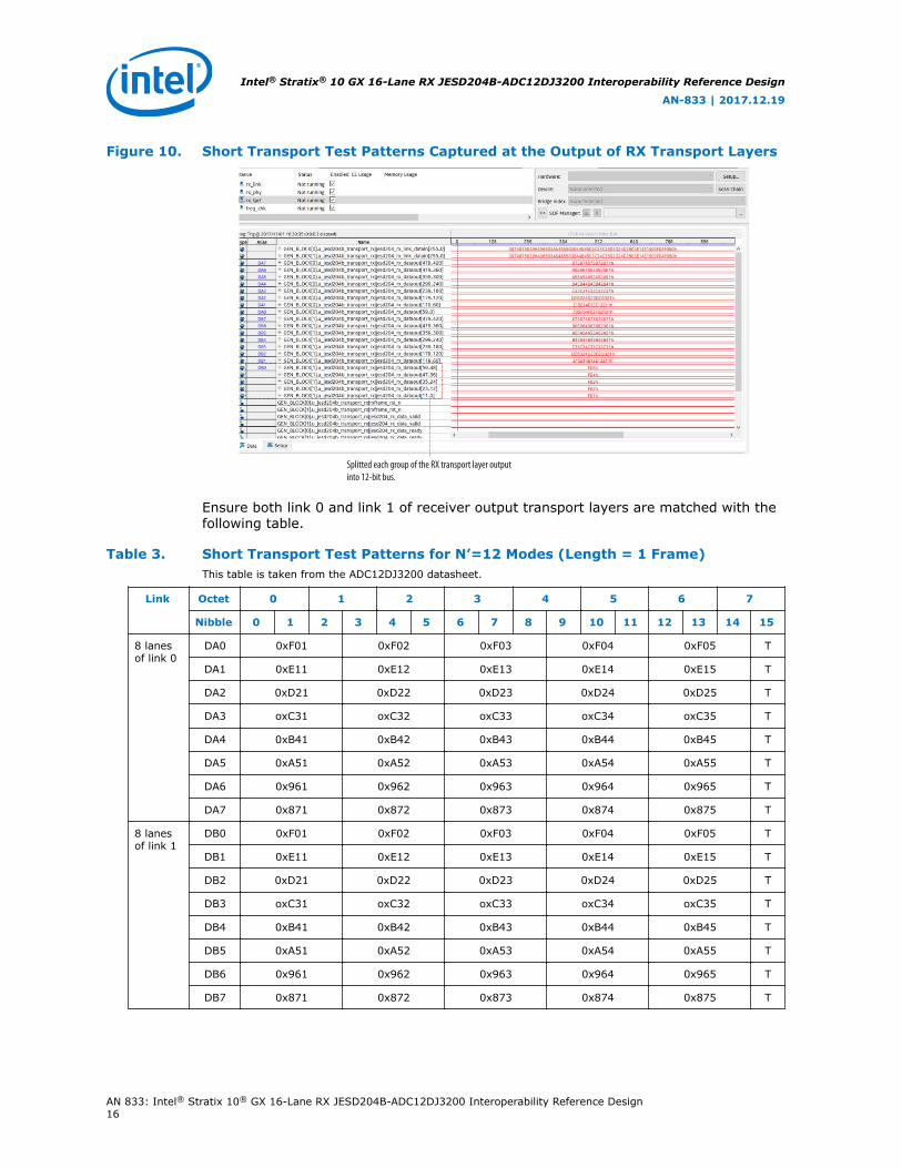
Figure 10. Short Transport Test Patterns Captured at the Output of RX Transport Layers
Splitted each group of the RX transport layer output into 12-bit bus.
Ensure both link 0 and link 1 of receiver output transport layers are matched with thefollowing table.
Table 3. Short Transport Test Patterns for N’=12 Modes (Length = 1 Frame)This table is taken from the ADC12DJ3200 datasheet.
Link Octet 0 1 2 3 4 5 6 7
Nibble 0 1 2 3 4 5 6 7 8 9 10 11 12 13 14 15
8 lanesof link 0
DA0 0xF01 0xF02 0xF03 0xF04 0xF05 T
DA1 0xE11 0xE12 0xE13 0xE14 0xE15 T
DA2 0xD21 0xD22 0xD23 0xD24 0xD25 T
DA3 oxC31 oxC32 oxC33 oxC34 oxC35 T
DA4 0xB41 0xB42 0xB43 0xB44 0xB45 T
DA5 0xA51 0xA52 0xA53 0xA54 0xA55 T
DA6 0x961 0x962 0x963 0x964 0x965 T
DA7 0x871 0x872 0x873 0x874 0x875 T
8 lanesof link 1
DB0 0xF01 0xF02 0xF03 0xF04 0xF05 T
DB1 0xE11 0xE12 0xE13 0xE14 0xE15 T
DB2 0xD21 0xD22 0xD23 0xD24 0xD25 T
DB3 oxC31 oxC32 oxC33 oxC34 oxC35 T
DB4 0xB41 0xB42 0xB43 0xB44 0xB45 T
DB5 0xA51 0xA52 0xA53 0xA54 0xA55 T
DB6 0x961 0x962 0x963 0x964 0x965 T
DB7 0x871 0x872 0x873 0x874 0x875 T
Intel® Stratix® 10 GX 16-Lane RX JESD204B-ADC12DJ3200 Interoperability Reference Design
AN-833 | 2017.12.19
AN 833: Intel® Stratix 10® GX 16-Lane RX JESD204B-ADC12DJ3200 Interoperability Reference Design16

Related Links
ADC12DJ3200 6.4-GSPS Single Channel or 3.2-GSPS Dual Channel, 12-bit, RF-Sampling Analog-to-Digital Converter (ADC) document
Provides more information about the ADC12DJ3200 EVM.
Verifying Ramp Pattern at Output Data of DLL to the Input Receiver Transport Layer
You can run the ramp test mode after running the short transport pattern test. In thismode, the JESD04B link layers operate normally, but the transport layers are disabled.After the initial lane alignment sequence (ILAS), each lane transmits an identical octetstream that increments from 0x00 to 0xFF and repeats.
To verify the ramp pattern at output data of DLL to the input receiver transport layer,follow these steps:
1. Change the command in line 7 of the ADC12DJxx00_JMODE1.cfg file to: 0x02050x04 // Set JTEST to 4 gives ramp test mode.
2. Reprogram the clocks and ADC.
3. Reconfigure the FPGA.
4. Type the start_basic_test procedure in the System Console Tcl Console toexecute the .tcl script to initialize the JESD204B links.
5. In the Instance Manager, click rx_link ➤ run Analysis.
6. If you want to check the JESD204B link up process, set a trigger condition to thedev_sync_n signal. The signal tap waits for trigger condition to occur. The triggercondition should occur once you execute the start_basic_test procedure.
Figure 11. Octet Ramp Pattern Captured at the Output of DLL
Related Links
• Setting Up the TI ADC12DJxx00 GUI Software and Board on page 9Provides the steps to reprogram the clocks and ADC.
• Configuring the FPGA on page 10
Deterministic Latency Test Results
A system is deterministic if latency is repeatable from power-up cycle to power-upcycle. In this design, the JESD204B IP cores are configured as subclass 1 mode tosupport deterministic latency. The TI ADC12DJ3200 EVM uses AC coupling for
Intel® Stratix® 10 GX 16-Lane RX JESD204B-ADC12DJ3200 Interoperability Reference Design
AN-833 | 2017.12.19
AN 833: Intel® Stratix 10® GX 16-Lane RX JESD204B-ADC12DJ3200 Interoperability Reference Design17

SYSREF+/-, thus the periodic SYSREF signal is required to achieve deterministiclatency. The SYSREF period from LMK04828 is configured to run at a frequency equalsto the Local Multi-Frame Clock (LMFC) frequency before the SYSREF signal is suppliedto the ADC and FPGA. The SYSREF pulse restarts the LMFC counter on the JESD204BIP cores and converter device, and realigns the LMFC counter to the LMFC boundary.
To ensure the deterministic latency in the reference design, follow these steps:
1. Check the FPGA SYSREF single detection.
For detailed description of the registers in the JESD204B RX IP core, refer to theAddressmap Information for 'altera_jesd204_rx_regmap'.
Passing criteria: The value of csr_sysref_singledet andcsr_sysref_lmfc_err should be zero.
Figure 12. csr_sysref_singledet and csr_sysref_lmfc_err Observed from the .tclConsole
syncn_sysref_ctrl[2] represents csr_sysref_singledet. This bit is zero when SYSREF is sampled.
syncn_sysref_ctrl[1] represents csr_sysref_alwayson. This bit is one indicating SYSREF continuous detection.
rx_err0[1] for link 0 and link1 is zero when SYSREF period matches the LMFC counter.
2. Check the SYSREF captured.Passing criteria: If the SYSREF is sampled correctly, the LMFC counter should bereset. Thus, the RBD_count value should only drift within 1–2 link clocks fromone power cycle to another power cycle. In this test, the RBD_count isconsistently 1 across 5 power cycle tests. It means the /R/ character isconsistently received at 1 LMFC count before the next LMFC boundary for 5 powercycle tests.
Intel® Stratix® 10 GX 16-Lane RX JESD204B-ADC12DJ3200 Interoperability Reference Design
AN-833 | 2017.12.19
AN 833: Intel® Stratix 10® GX 16-Lane RX JESD204B-ADC12DJ3200 Interoperability Reference Design18

Figure 13. Early RBD Release Opportunity for Latest Arrival Lane Within One LMFC
0 1 2 3 4 5 6 7 0 1 2
K K K K K K K R D D D
K K K K K K K R D D D
K K K K K K K R D D D
Current LMFCBoundary
Next LMFCBoundary
RBD Elastic Buffer Size = 8
RBD Count = 1
K K K K K K K R D D D
K K K K K K K R D D D
RBD Count = 1
RBD Count = 1
RBD Count = 1
RBD Count = 1
Link Clock
SYNC_IN
Internal LMFC Counter
Latest Arrival Lane in First Power Cycle
Latest Arrival Lane in Second Power Cycle
Latest Arrival Lane in Fifth Power Cycle
Latest Arrival Lane in Fourth Power Cycle
Latest Arrival Lane in Third Power Cycle
3. Check the latency from the start of combined SYNC_N deassertion output from thetwo JESD204B IP cores to the first user data output.Passing criteria: You should observe consistent latency from the start of combinedSYNC_n deassertion to the assertion of the jesd204_rx_link_valid signal. Inthis design test, you should consistently observe 67 link cycles clock from onepower cycle to another.
Figure 14. Measured Latency from the Start of Combined SYNC_n to the First User DataOutput
4. Ensure the data latency is fixed during user data phase.Passing criteria: The ramp pattern should be in perfect shape with no distortion.
Figure 15. Ramp Pattern in Perfect Shape
Intel® Stratix® 10 GX 16-Lane RX JESD204B-ADC12DJ3200 Interoperability Reference Design
AN-833 | 2017.12.19
AN 833: Intel® Stratix 10® GX 16-Lane RX JESD204B-ADC12DJ3200 Interoperability Reference Design19

Related Links
Addressmap Information for 'altera_jesd204_rx_regmap'Provides detailed description of the registers in the JESD204B RX IP core.
Rebuilding Design
You need to regenerate the platform designer system if you want to modify thesystem, such as IP components settings and interfaces.
To regenerate the HDL files for the top level platform designer system, follow thesesteps:
1. Open altera_jesd204_ed_qsys_RX.qsys.
2. In the platform designer GUI, click Generate ➤ Generate HDL.
Note: If you want to modify the JESD204B IP cores, Transceiver PHY ResetController, and other component settings, right click on thealtera_jesd204_subsystem_RX component and select Drill intoSubsystem. After the modification, save the system. Go back to the toplevel platform designer system file and generate the HDL files.
3. To rerun design in hardware, follow the steps in the Running the Reference Designsection.
Related Links
Running the Reference Design on page 8Provides the steps to rerun the reference design.
Procedures in the main.tcl System Console Script
Table 4. Procedures in the main.tcl System Console Script
Procedure Value Description
start_basic_test — Main procedure that performs global reset, set checker test mode,enable SYSREF continuous detection mode, clear JESD204B IPcores error status registers, and report link status.
reset — Perform global reset.
force_link_frame_reset
0, 1 0: Deassert link and frame reset.1: Assert and hold link and frame reset.Note: Link and frame clock domains should be held in reset while
writing to the JESD204B IP control and status register(CSR).
set_testmode alt, ramp, prbs alt: Set pattern checker to alternate pattern.ramp: Set pattern checker to ramp pattern.prbs: Set pattern checker to pseudo-random binary sequence(PRBS) pattern.
sysref_con — Enable SYSREF continuous detection with SYSREF single detection.
rbd_offset integer Adjust RBD offset value to eliminate RX lane deskew error ifneeded. Refer to the JESD204B IP Core User Guide for moredetails.
continued...
Intel® Stratix® 10 GX 16-Lane RX JESD204B-ADC12DJ3200 Interoperability Reference Design
AN-833 | 2017.12.19
AN 833: Intel® Stratix 10® GX 16-Lane RX JESD204B-ADC12DJ3200 Interoperability Reference Design20

Procedure Value Description
read_status_pio — Read the status of the parallel I/O (PIO) registers. The PIO statushas the following configurations:• Bit 0—Core PLL locked• Bit 1—RX transceiver ready (Link 0)• Bit 2—RX link error (Link 0)• Bit 3—RX transceiver ready (Link 1)• Bit 4—RX link error (Link 1)Note: Use the read_err_status procedure to report error in
description.
read_err_status — Read the JESD204B IP error status registers. For detaileddescription of the status registers, refer to the AddressmapInformation for 'altera_jesd204_rx_regmap'.
clear_err_status — Clear the JESD204B IP error status registers.
read_rx_status0 — Read JESD204B IP rx_status0 register. For detailed description ofthe status registers, refer to the Addressmap Information for'altera_jesd204_rx_regmap'.
wait_seconds integer Set to wait for integer seconds.
eval_test — Report the link status.
Related Links
Programmable RBD Offset, JESD204B IP Core User GuideProvides more information on adjusting the RBD offset value.
Document Revision History for AN 833: Intel Stratix 10 GX 16-LaneRX JESD204B-ADC12DJ3200 Interoperability Reference Design
Date Version Changes
December 2017 2017.12.19 Initial release.
Intel® Stratix® 10 GX 16-Lane RX JESD204B-ADC12DJ3200 Interoperability Reference Design
AN-833 | 2017.12.19
AN 833: Intel® Stratix 10® GX 16-Lane RX JESD204B-ADC12DJ3200 Interoperability Reference Design21