256k x 16 high speed asynchronous cmos static · pdf file2 integrated silicon solution, inc....
TRANSCRIPT
Integrated Silicon Solution, Inc. — www.issi.com 1Rev. H102/10/2017
Copyright © 2017 Integrated Silicon Solution, Inc. All rights reserved. ISSI reserves the right to make changes to this specification and its products at any time without notice. ISSI assumes no liability arising out of the application or use of any information, products or services described herein. Customers are advised to obtain the lat-est version of this device specification before relying on any published information and before placing orders for products.
Integrated Silicon Solution, Inc. does not recommend the use of any of its products in life support applications where the failure or malfunction of the product can reason-ably be expected to cause failure of the life support system or to significantly affect its safety or effectiveness. Products are not authorized for use in such applications unless Integrated Silicon Solution, Inc. receives written assurance to its satisfaction, that:a.) the risk of injury or damage has been minimized;b.) the user assume all such risks; andc.) potential liability of Integrated Silicon Solution, Inc is adequately protected under the circumstances
IS61WV25616ALL/ALSIS61WV25616BLL/BLSIS64WV25616BLL/BLS
FEATURESHIGH SPEED: (IS61/64WV25616ALL/BLL)
• High-speedaccesstime:8,10,20ns
• LowActivePower:85mW(typical)
• LowStandbyPower:7mW(typical) CMOS standby
LOW POWER: (IS61/64WV25616ALS/BLS)
• High-speedaccesstime:25,35,45ns
• LowActivePower:35mW(typical)
• LowStandbyPower:0.6mW(typical) CMOS standby
• Singlepowersupply
— Vdd 1.65V to 2.2V (IS61WV25616Axx)
— Vdd2.4Vto3.6V(IS61/64WV25616Bxx)
• Fullystaticoperation:noclockorrefreshrequired
• Threestateoutputs
• Datacontrolforupperandlowerbytes
• IndustrialandAutomotivetemperaturesupport
• Lead-freeavailable
256K x 16 HIGH SPEED ASYNCHRONOUS CMOS STATIC RAM
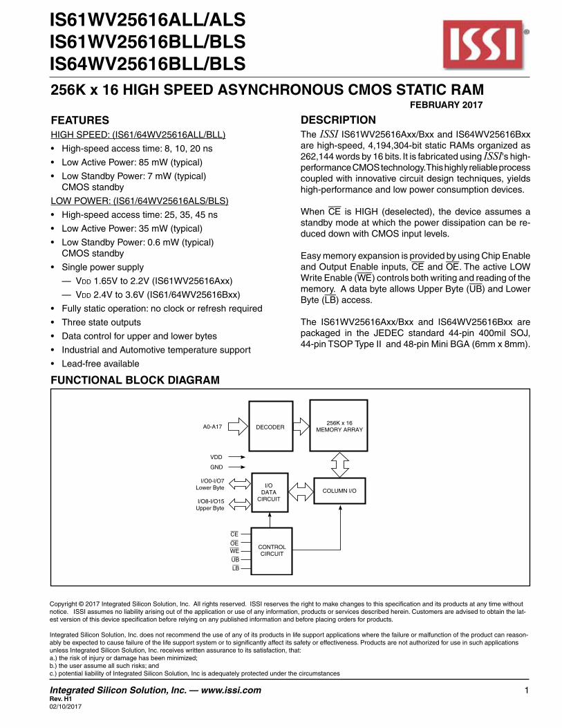
DESCRIPTIONTheISSI IS61WV25616Axx/Bxx and IS64WV25616Bxx arehigh-speed,4,194,304-bitstaticRAMsorganizedas262,144 words by 16 bits. It is fabricated using ISSI's high-performanceCMOStechnology.Thishighlyreliableprocesscoupled with innovative circuit design techniques, yields high-performance and low power consumption devices.
When CE is HIGH (deselected), the device assumes a standby mode at which the power dissipation can be re-duced down with CMOS input levels.
Easy memory expansion is provided by using Chip Enable and Output Enable inputs, CE and OE.TheactiveLOWWrite Enable (WE) controls both writing and reading of the memory. A data byte allows Upper Byte (UB) and Lower Byte (LB) access.
The IS61WV25616Axx/Bxx and IS64WV25616Bxx arepackaged in the JEDEC standard 44-pin 400mil SOJ, 44-pinTSOPTypeIIand48-pinMiniBGA(6mmx8mm).
FUNCTIONAL BLOCK DIAGRAM
A0-A17
CE
OEWE
256K x 16MEMORY ARRAYDECODER
COLUMN I/O
CONTROLCIRCUIT
GND
VDD
I/ODATA
CIRCUIT
I/O0-I/O7Lower Byte
I/O8-I/O15Upper Byte
UB
LB
FEBRUARY 2017
2 Integrated Silicon Solution, Inc. — www.issi.comRev. H1
02/10/2017
IS61WV25616ALL/ALS, IS61WV25616BLL/BLS, IS64WV25616BLL/BLS
TRUTH TABLE I/O PIN
Mode WE CE OE LB UB I/O0-I/O7 I/O8-I/O15 VDD Current
Not Selected X H X X X High-Z High-Z Isb1, Isb2
Output Disabled H L H X X High-Z High-Z Icc X L X H H High-Z High-Z
Read H L L L H dout High-Z Icc H L L H L High-Z dout H L L L L dout dout
Write L L X L H dIn High-Z Icc L L X H L High-Z dIn L L X L L dIn dIn
PIN DESCRIPTIONSA0-A17 Address Inputs
I/O0-I/O15 Data Inputs/Outputs
CE Chip Enable Input
OE Output Enable Input
WE Write Enable Input
LB Lower-byte Control (I/O0-I/O7)
UB Upper-byteControl(I/O8-I/O15)
NC No Connection
Vdd Power
GND Ground
12345678910111213141516171819202122
44434241403938373635343332313029282726252423
A0A1A2A3A4CE
I/O0I/O1I/O2I/O3VDDGNDI/O4I/O5I/O6I/O7WEA5A6A7A8A9
A17A16A15OEUBLBI/O15I/O14I/O13I/O12GNDVDDI/O11I/O10I/O9I/O8NCA14A13A12A11A10
PIN CONFIGURATIONS
44-Pin TSOP (Type II) and SOJ
*soJ package under evaluation.
Integrated Silicon Solution, Inc. — www.issi.com 3Rev. H102/10/2017
IS61WV25616ALL/ALS, IS61WV25616BLL/BLS, IS64WV25616BLL/BLS
1234567891011
3332313029282726252423
12 13 14 15 16 17 18 19 20 21 22
44 43 42 41 40 39 38 37 36 35 34CE
I/O0I/O1I/O2I/O3VDDGNDI/O4I/O5I/O6I/O7
I/O15I/O14I/O13I/O12GNDVDDI/O11I/O10I/O9I/O8NC
TOP VIEW
WE
A0
A1
A2
A3
A4
A5
A6
A7
A8
A9
A1
7A
16
A1
5A
14
A1
3A
12
A1
1A
10
OE
UB
LB
1 2 3 4 5 6
A
B
C
D
E
F
G
H
LB OE A0 A1 A2 N/C
I/O8 UB A3 A4 CE I/O0
I/O9 I/O10 A5 A6 I/O1 I/O2
GND I/O11 A17 A7 I/O3 VDD
VDD I/O12 NC A16 I/O4 GND
I/O14 I/O13 A14 A15 I/O5 I/O6
I/O15 NC A12 A13 WE I/O7
NC A8 A9 A10 A11 NC
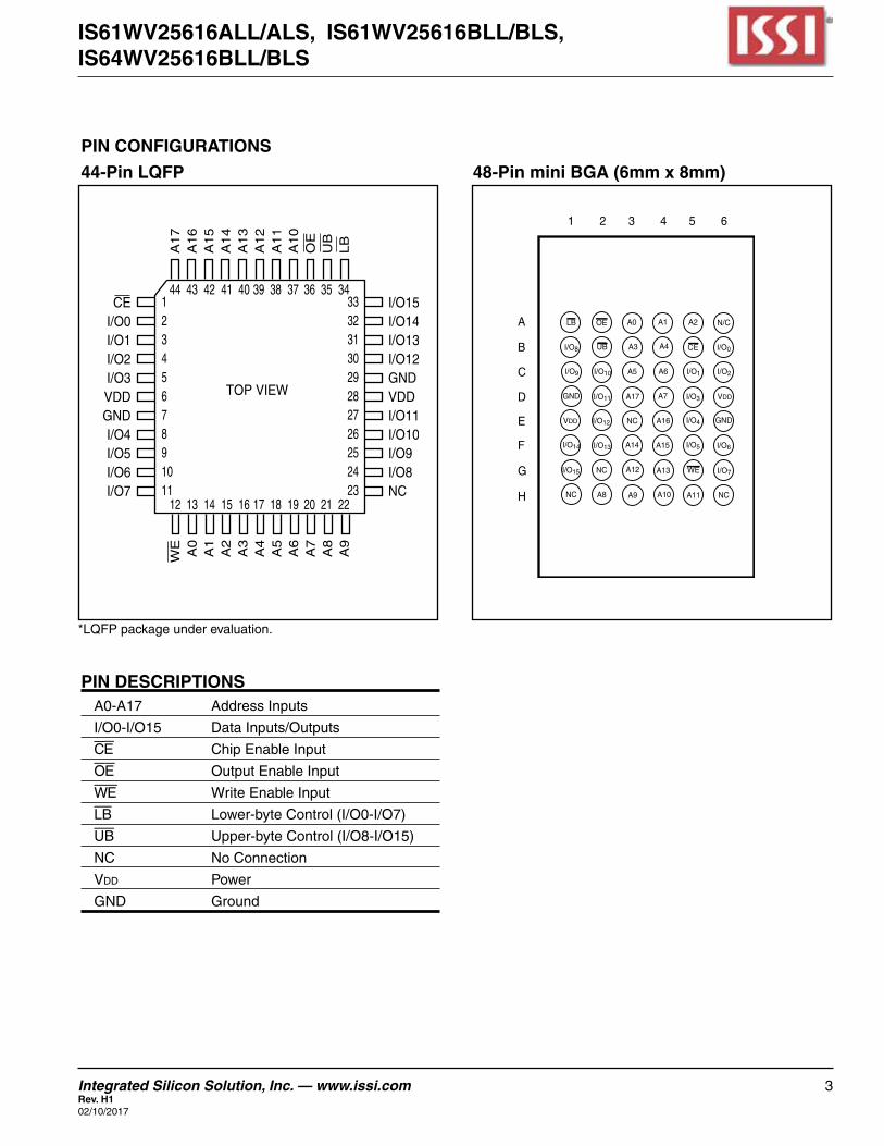
48-Pin mini BGA (6mm x 8mm)
PIN CONFIGURATIONS
44-Pin LQFP
PIN DESCRIPTIONSA0-A17 Address Inputs
I/O0-I/O15 Data Inputs/Outputs
CE Chip Enable Input
OE Output Enable Input
WE Write Enable Input
LB Lower-byte Control (I/O0-I/O7)
UB Upper-byteControl(I/O8-I/O15)
NC No Connection
Vdd Power
GND Ground
*LQFP package under evaluation.
4 Integrated Silicon Solution, Inc. — www.issi.comRev. H1
02/10/2017
IS61WV25616ALL/ALS, IS61WV25616BLL/BLS, IS64WV25616BLL/BLS
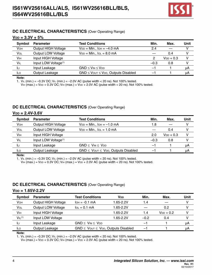
DC ELECTRICAL CHARACTERISTICS (Over Operating Range)
VDD = 2.4V-3.6V
Symbol Parameter Test Conditions Min. Max. Unit
VoH Output HIGH Voltage Vdd = Min., IoH = –1.0mA 1.8 — V
VoL Output LOW Voltage Vdd = Min., IoL = 1.0 mA — 0.4 V
VIH Input HIGH Voltage 2.0 Vdd + 0.3 V
VIL Input LOW Voltage(1) –0.3 0.8 V
ILI Input Leakage GND ≤ VIn ≤ Vdd –1 1 µA
ILo Output Leakage GND ≤ Vout ≤ Vdd, Outputs Disabled –1 1 µANote:1. VIL (min.) = –0.3V DC; VIL (min.) = –2.0V AC (pulse width < 20 ns). Not 100% tested. VIH (max.) = Vdd + 0.3V dc; VIH (max.) = Vdd + 2.0V Ac (pulse width < 20 ns). Not 100% tested.
DC ELECTRICAL CHARACTERISTICS (Over Operating Range)
VDD = 3.3V + 5% Symbol Parameter Test Conditions Min. Max. Unit VoH Output HIGH Voltage Vdd = Min., IoH = –4.0 mA 2.4 — V VoL Output LOW Voltage Vdd = Min., IoL = 8.0mA — 0.4 V VIH Input HIGH Voltage 2 Vdd + 0.3 V VIL Input LOW Voltage(1) –0.3 0.8 V ILI Input Leakage GND ≤ VIn ≤ Vdd –1 1 µA ILo Output Leakage GND ≤ Vout ≤ Vdd, Outputs Disabled –1 1 µA
Note:1. VIL (min.) = –0.3V DC; VIL (min.) = –2.0V AC (pulse width < 20 ns). Not 100% tested. VIH (max.) = Vdd + 0.3V dc; VIH (max.) = Vdd + 2.0V Ac (pulse width < 20 ns). Not 100% tested.
DC ELECTRICAL CHARACTERISTICS (Over Operating Range)
VDD = 1.65V-2.2V
Symbol Parameter Test Conditions VDD Min. Max. Unit
VoH Output HIGH Voltage IoH = -0.1 mA 1.65-2.2V 1.4 — V
VoL Output LOW Voltage IoL = 0.1 mA 1.65-2.2V — 0.2 V
VIH Input HIGH Voltage 1.65-2.2V 1.4 Vdd + 0.2 V
VIL(1) Input LOW Voltage 1.65-2.2V –0.2 0.4 V
ILI Input Leakage GND ≤ VIn ≤ Vdd –1 1 µA
ILo Output Leakage GND ≤ Vout ≤ Vdd, Outputs Disabled –1 1 µANote:1. VIL (min.) = –0.3V DC; VIL (min.) = –2.0V AC (pulse width < 20 ns). Not 100% tested. VIH (max.) = Vdd + 0.3V dc; VIH (max.) = Vdd + 2.0V Ac (pulse width < 20 ns). Not 100% tested.
Integrated Silicon Solution, Inc. — www.issi.com 5Rev. H102/10/2017
IS61WV25616ALL/ALS, IS61WV25616BLL/BLS, IS64WV25616BLL/BLS
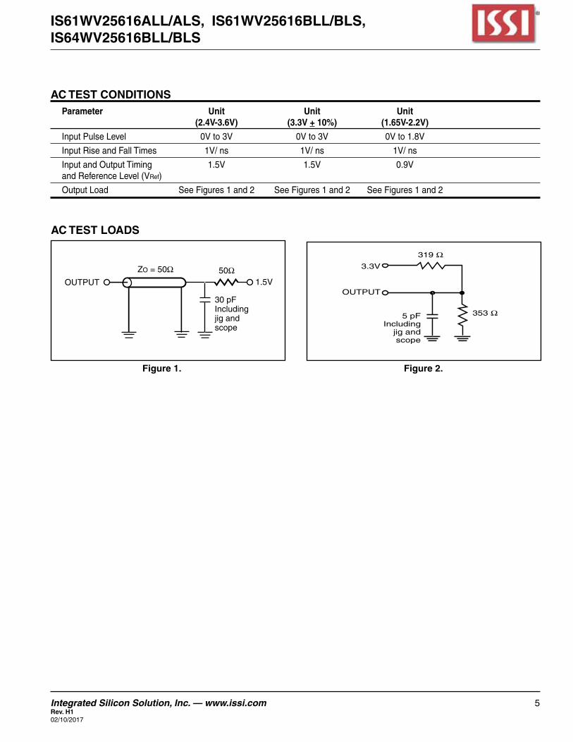
AC TEST LOADS
Figure 1.
319 Ω
5 pFIncluding
jig andscope
353 Ω
OUTPUT
3.3V
Figure 2.
ZO = 50Ω 1.5V
50ΩOUTPUT
30 pFIncludingjig andscope
AC TEST CONDITIONS Parameter Unit Unit Unit (2.4V-3.6V) (3.3V + 10%) (1.65V-2.2V)
InputPulseLevel 0Vto3V 0Vto3V 0Vto1.8V
InputRiseandFallTimes 1V/ns 1V/ns 1V/ns
InputandOutputTiming 1.5V 1.5V 0.9V and Reference Level (VRef)
OutputLoad SeeFigures1and2 SeeFigures1and2 SeeFigures1and2
6 Integrated Silicon Solution, Inc. — www.issi.comRev. H1
02/10/2017
IS61WV25616ALL/ALS, IS61WV25616BLL/BLS, IS64WV25616BLL/BLS
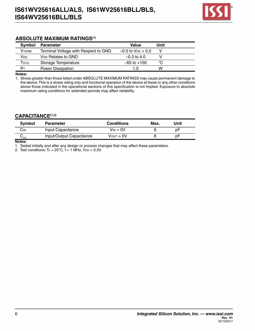
ABSOLUTE MAXIMUM RATINGS(1)
Symbol Parameter Value Unit Vterm TerminalVoltagewithRespecttoGND –0.5toVdd + 0.5 V Vdd VddRelatestoGND –0.3to4.0 V tstg StorageTemperature –65to+150 °C Pt Power Dissipation 1.0 WNotes:1.StressgreaterthanthoselistedunderABSOLUTEMAXIMUMRATINGSmaycausepermanentdamageto
thedevice.Thisisastressratingonlyandfunctionaloperationofthedeviceattheseoranyotherconditionsabove those indicated in the operational sections of this specification is not implied. Exposure to absolute maximum rating conditions for extended periods may affect reliability.
CAPACITANCE(1,2)
Symbol Parameter Conditions Max. Unit
cIn Input Capacitance VIn = 0V 6 pF
cI/o Input/Output Capacitance Vout = 0V 8 pFNotes:1.Testedinitiallyandafteranydesignorprocesschangesthatmayaffecttheseparameters.2. Testconditions:TA = 25°c, f = 1 MHz, Vdd=3.3V.
Integrated Silicon Solution, Inc. — www.issi.com 7Rev. H102/10/2017
IS61WV25616ALL/ALS, IS61WV25616BLL/BLS, IS64WV25616BLL/BLS
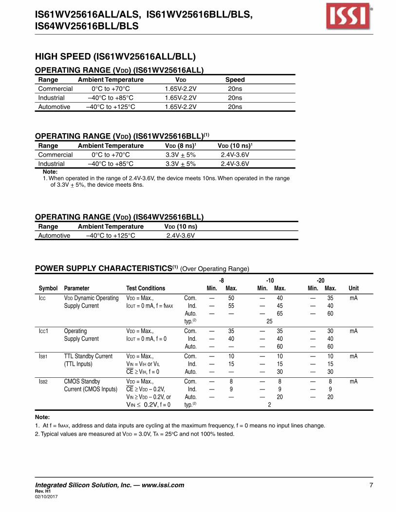
OPERATING RANGE (VDD) (IS61WV25616BLL)(1)
Range Ambient Temperature VDD (8 nS)1 VDD (10 nS)1
Commercial 0°Cto+70°C 3.3V+5% 2.4V-3.6V Industrial –40°Cto+85°C 3.3V+5% 2.4V-3.6V
Note:1.Whenoperatedintherangeof2.4V-3.6V,thedevicemeets10ns.Whenoperatedintherange
of3.3V+5%,thedevicemeets8ns.
OPERATING RANGE (VDD) (IS64WV25616BLL) Range Ambient Temperature VDD (10 nS) Automotive –40°Cto+125°C 2.4V-3.6V
HIGH SPEED (IS61WV25616ALL/BLL)OPERATING RANGE (VDD) (IS61WV25616ALL) Range Ambient Temperature VDD Speed Commercial 0°Cto+70°C 1.65V-2.2V 20ns Industrial –40°Cto+85°C 1.65V-2.2V 20ns Automotive –40°Cto+125°C 1.65V-2.2V 20ns
POWER SUPPLY CHARACTERISTICS(1) (Over Operating Range)
-8 -10 -20 Symbol Parameter Test Conditions Min. Max. Min. Max. Min. Max. Unit
Icc Vdd Dynamic Operating Vdd = Max., Com. — 50 — 40 — 35 mA Supply Current Iout = 0 mA, f = fmAX Ind. — 55 — 45 — 40 Auto. — — — 65 — 60 typ.(2) 25
Icc1 Operating Vdd = Max., Com. — 35 — 35 — 30 mA Supply Current Iout = 0 mA, f = 0 Ind. — 40 — 40 — 40 Auto. — — — 60 — 60
Isb1 TTLStandbyCurrent Vdd = Max., Com. — 10 — 10 — 10 mA (TTLInputs) VIn = VIH or VIL Ind. — 15 — 15 — 15 CE ≥ VIH,f=0 Auto. — — — 30 — 30
Isb2 CMOS Standby Vdd = Max., Com. — 8 — 8 — 8 mA Current (CMOS Inputs) CE ≥ Vdd – 0.2V, Ind. — 9 — 9 — 9 VIn ≥ Vdd – 0.2V, or Auto. — — — 20 — 20 VIn ≤ 0.2V, f = 0 typ.(2) 2
Note:1. At f = fmAX, address and data inputs are cycling at the maximum frequency, f = 0 means no input lines change.2.TypicalvaluesaremeasuredatVdd=3.0V,TA = 25oC and not 100% tested.
8 Integrated Silicon Solution, Inc. — www.issi.comRev. H1
02/10/2017
IS61WV25616ALL/ALS, IS61WV25616BLL/BLS, IS64WV25616BLL/BLS
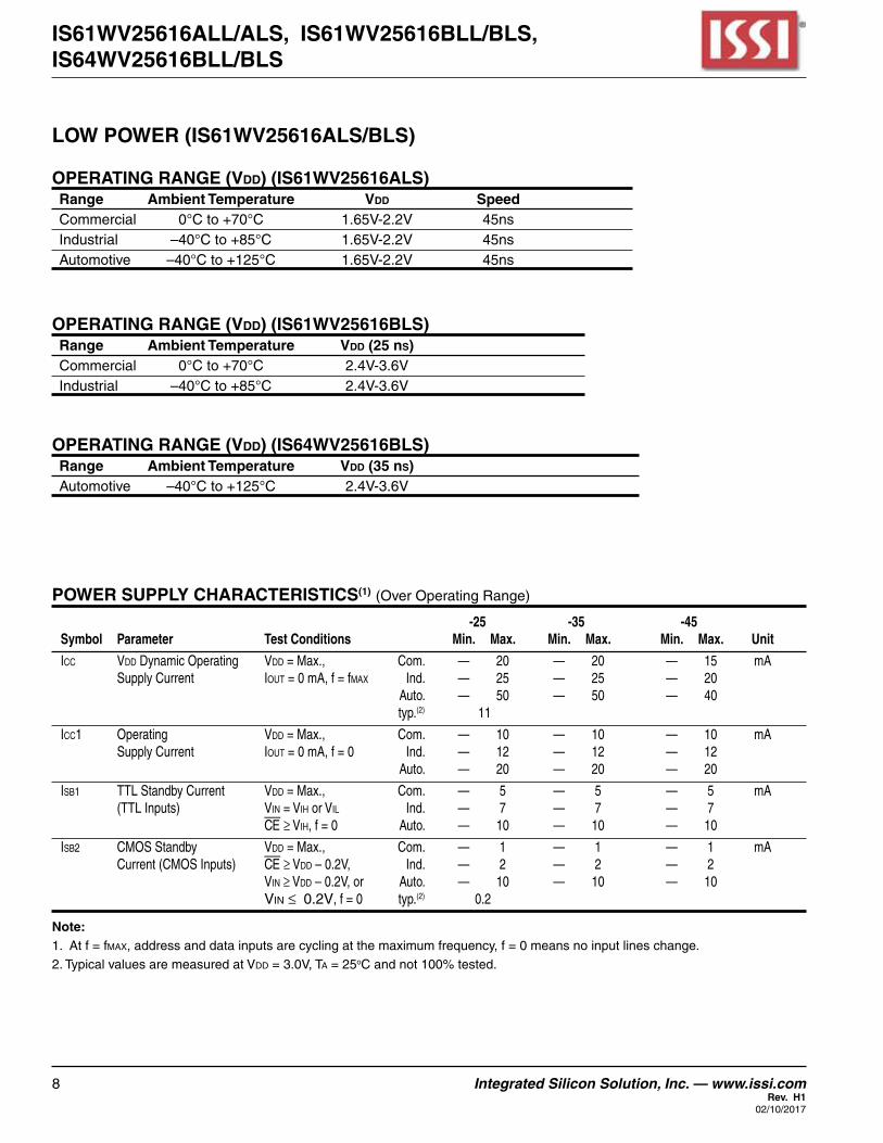
POWER SUPPLY CHARACTERISTICS(1) (Over Operating Range)
-25 -35 -45 Symbol Parameter Test Conditions Min. Max. Min. Max. Min. Max. Unit
Icc Vdd Dynamic Operating Vdd = Max., Com. — 20 — 20 — 15 mA Supply Current Iout = 0 mA, f = fmAX Ind. — 25 — 25 — 20 Auto. — 50 — 50 — 40 typ.(2) 11
Icc1 Operating Vdd = Max., Com. — 10 — 10 — 10 mA Supply Current Iout = 0 mA, f = 0 Ind. — 12 — 12 — 12 Auto. — 20 — 20 — 20
Isb1 TTLStandbyCurrent Vdd = Max., Com. — 5 — 5 — 5 mA (TTLInputs) VIn = VIH or VIL Ind. — 7 — 7 — 7 CE ≥ VIH, f = 0 Auto. — 10 — 10 — 10
Isb2 CMOS Standby Vdd = Max., Com. — 1 — 1 — 1 mA Current (CMOS Inputs) CE ≥ Vdd – 0.2V, Ind. — 2 — 2 — 2 VIn ≥ Vdd – 0.2V, or Auto. — 10 — 10 — 10 VIn ≤ 0.2V, f = 0 typ.(2) 0.2
Note:1. At f = fmAX, address and data inputs are cycling at the maximum frequency, f = 0 means no input lines change.2.TypicalvaluesaremeasuredatVdd=3.0V,TA = 25oC and not 100% tested.
OPERATING RANGE (VDD) (IS61WV25616BLS) Range Ambient Temperature VDD (25 nS) Commercial 0°Cto+70°C 2.4V-3.6V Industrial –40°Cto+85°C 2.4V-3.6V
LOW POWER (IS61WV25616ALS/BLS)
OPERATING RANGE (VDD) (IS61WV25616ALS) Range Ambient Temperature VDD Speed Commercial 0°Cto+70°C 1.65V-2.2V 45ns Industrial –40°Cto+85°C 1.65V-2.2V 45ns Automotive –40°Cto+125°C 1.65V-2.2V 45ns
OPERATING RANGE (VDD) (IS64WV25616BLS) Range Ambient Temperature VDD (35 nS) Automotive –40°Cto+125°C 2.4V-3.6V
Integrated Silicon Solution, Inc. — www.issi.com 9Rev. H102/10/2017
IS61WV25616ALL/ALS, IS61WV25616BLL/BLS, IS64WV25616BLL/BLS
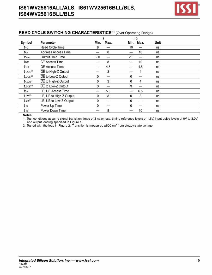
READ CYCLE SWITCHING CHARACTERISTICS(1) (Over Operating Range)
-8 -10 Symbol Parameter Min. Max. Min. Max. Unit trc ReadCycleTime 8 — 10 — ns tAA AddressAccessTime — 8 — 10 ns toHA OutputHoldTime 2.0 — 2.0 — ns tAce CEAccessTime — 8 — 10 ns tdoe OEAccessTime — 4.5 — 4.5 ns tHzoe(2) OEtoHigh-ZOutput — 3 — 4 ns tLzoe(2) OE to Low-Z Output 0 — 0 — ns tHzce(2 CEtoHigh-ZOutput 0 3 0 4 ns tLzce(2) CEtoLow-ZOutput 3 — 3 — ns tbA LB, UBAccessTime — 5.5 — 6.5 ns tHzb(2) LB, UBtoHigh-ZOutput 0 3 0 3 ns tLzb(2) LB, UB to Low-Z Output 0 — 0 — ns tPu PowerUpTime 0 — 0 — ns tPd PowerDownTime — 8 — 10 ns
Notes: 1. Testconditionsassumesignaltransitiontimesof3nsorless,timingreferencelevelsof1.5V,inputpulselevelsof0Vto3.0V
andoutputloadingspecifiedinFigure1.2. TestedwiththeloadinFigure2.Transitionismeasured±500mVfromsteady-statevoltage.
10 Integrated Silicon Solution, Inc. — www.issi.comRev. H1
02/10/2017
IS61WV25616ALL/ALS, IS61WV25616BLL/BLS, IS64WV25616BLL/BLS
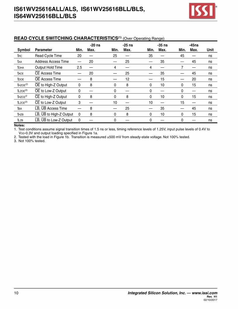
READ CYCLE SWITCHING CHARACTERISTICS(1) (Over Operating Range)
-20 ns -25 ns -35 ns -45ns Symbol Parameter Min. Max. Min. Max. Min. Max. Min. Max. Unit
trc ReadCycleTime 20 — 25 — 35 — 45 — ns
tAA AddressAccessTime — 20 — 25 — 35 — 45 ns
toHA OutputHoldTime 2.5 — 4 — 4 — 7 — ns
tAce CEAccessTime — 20 — 25 — 35 — 45 ns
tdoe OEAccessTime — 8 — 12 — 15 — 20 ns
tHzoe(2) OEtoHigh-ZOutput 0 8 0 8 0 10 0 15 ns
tLzoe(2) OE to Low-Z Output 0 — 0 — 0 — 0 — ns
tHzce(2 CEtoHigh-ZOutput 0 8 0 8 0 10 0 15 ns
tLzce(2) CEtoLow-ZOutput 3 — 10 — 10 — 15 — ns
tbA LB, UBAccessTime — 8 — 25 — 35 — 45 ns
tHzb LB, UBtoHigh-ZOutput 0 8 0 8 0 10 0 15 ns
tLzb LB, UB to Low-Z Output 0 — 0 — 0 — 0 — nsNotes: 1. Testconditionsassumesignaltransitiontimesof1.5nsorless,timingreferencelevelsof1.25V,inputpulselevelsof0.4Vto
Vdd-0.3VandoutputloadingspecifiedinFigure1a.2. TestedwiththeloadinFigure1b.Transitionismeasured±500mVfromsteady-statevoltage.Not100%tested.3. Not100%tested.
Integrated Silicon Solution, Inc. — www.issi.com 11Rev. H102/10/2017
IS61WV25616ALL/ALS, IS61WV25616BLL/BLS, IS64WV25616BLL/BLS
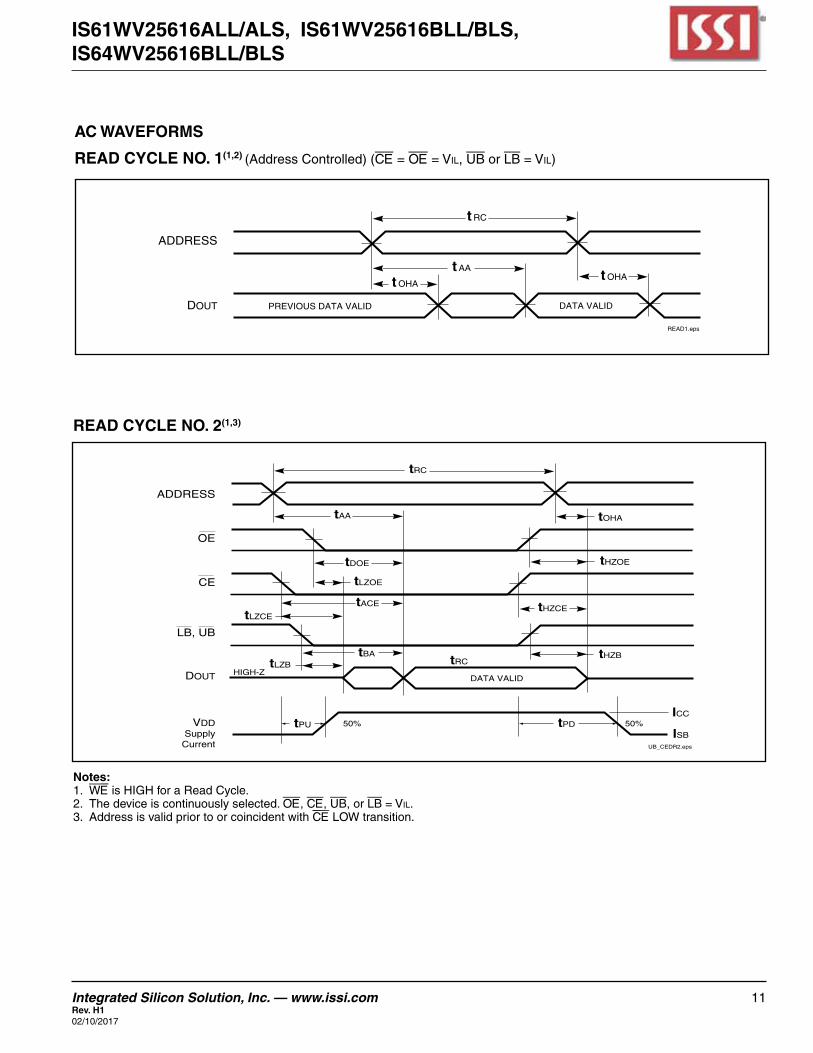
DATA VALID
READ1.eps
PREVIOUS DATA VALID
t AA
t OHAt OHA
t RC
DOUT
ADDRESS
AC WAVEFORMS
READ CYCLE NO. 1(1,2) (Address Controlled) (CE = OE = VIL, UB or LB = VIL)
tRC
tOHAtAA
tDOE
tLZOE
tACE
tLZCE
tHZOE
HIGH-ZDATA VALID
UB_CEDR2.eps
tHZB
ADDRESS
OE
CE
LB, UB
DOUT
tHZCE
tBAtLZB tRC
tPDISB
ICC50%VDD
SupplyCurrent
50%tPU
READ CYCLE NO. 2(1,3)
Notes: 1. WE is HIGH for a Read Cycle.2. Thedeviceiscontinuouslyselected.OE, CE, UB, or LB = VIL.3. AddressisvalidpriortoorcoincidentwithCE LOW transition.
12 Integrated Silicon Solution, Inc. — www.issi.comRev. H1
02/10/2017
IS61WV25616ALL/ALS, IS61WV25616BLL/BLS, IS64WV25616BLL/BLS
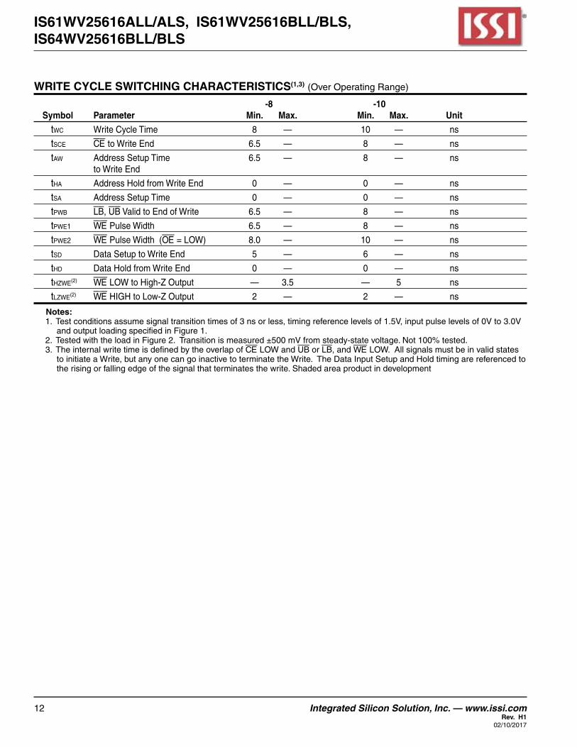
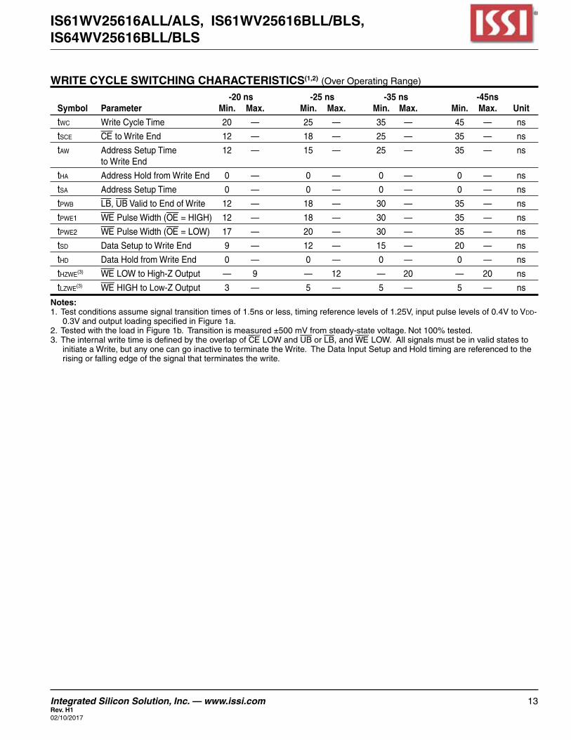
WRITE CYCLE SWITCHING CHARACTERISTICS(1,3) (Over Operating Range)
-8 -10 Symbol Parameter Min. Max. Min. Max. Unit
twc WriteCycleTime 8 — 10 — ns
tsce CEtoWriteEnd 6.5 — 8 — ns
tAw AddressSetupTime 6.5 — 8 — ns to Write End
tHA Address Hold from Write End 0 — 0 — ns
tsA AddressSetupTime 0 — 0 — ns
tPwb LB, UBValidtoEndofWrite 6.5 — 8 — ns
tPwe1 WEPulseWidth 6.5 — 8 — ns
tPwe2 WE Pulse Width (OE=LOW) 8.0 — 10 — ns
tsd Data Setup to Write End 5 — 6 — ns
tHd Data Hold from Write End 0 — 0 — ns
tHzwe(2) WELOWtoHigh-ZOutput — 3.5 — 5 ns
tLzwe(2) WE HIGH to Low-Z Output 2 — 2 — ns
Notes: 1. Testconditionsassumesignaltransitiontimesof3nsorless,timingreferencelevelsof1.5V,inputpulselevelsof0Vto3.0V
andoutputloadingspecifiedinFigure1.2. TestedwiththeloadinFigure2.Transitionismeasured±500mVfromsteady-statevoltage.Not100%tested.3. TheinternalwritetimeisdefinedbytheoverlapofCE LOW and UB or LB, and WE LOW. All signals must be in valid states
toinitiateaWrite,butanyonecangoinactivetoterminatetheWrite.TheDataInputSetupandHoldtimingarereferencedtothe rising or falling edge of the signal that terminates the write. Shaded area product in development
Integrated Silicon Solution, Inc. — www.issi.com 13Rev. H102/10/2017
IS61WV25616ALL/ALS, IS61WV25616BLL/BLS, IS64WV25616BLL/BLS
WRITE CYCLE SWITCHING CHARACTERISTICS(1,2) (Over Operating Range)
-20 ns -25 ns -35 ns -45ns Symbol Parameter Min. Max. Min. Max. Min. Max. Min. Max. Unit
twc WriteCycleTime 20 — 25 — 35 — 45 — ns
tsce CEtoWriteEnd 12 — 18 — 25 — 35 — ns
tAw AddressSetupTime 12 — 15 — 25 — 35 — ns to Write End
tHA Address Hold from Write End 0 — 0 — 0 — 0 — ns
tsA AddressSetupTime 0 — 0 — 0 — 0 — ns
tPwb LB, UBValidtoEndofWrite 12 — 18 — 30 — 35 — ns
tPwe1 WE Pulse Width (OE=HIGH) 12 — 18 — 30 — 35 — ns
tPwe2 WE Pulse Width (OE=LOW) 17 — 20 — 30 — 35 — ns
tsd Data Setup to Write End 9 — 12 — 15 — 20 — ns
tHd Data Hold from Write End 0 — 0 — 0 — 0 — ns
tHzwe(3) WE LOW to High-Z Output — 9 — 12 — 20 — 20 ns
tLzwe(3) WEHIGHtoLow-ZOutput 3 — 5 — 5 — 5 — ns
Notes: 1. Test conditions assume signal transition times of 1.5ns or less, timing reference levels of 1.25V, input pulse levels of 0.4V to Vdd-
0.3VandoutputloadingspecifiedinFigure1a.2. TestedwiththeloadinFigure1b.Transitionismeasured±500mVfromsteady-statevoltage.Not100%tested.3. TheinternalwritetimeisdefinedbytheoverlapofCE LOW and UB or LB, and WE LOW. All signals must be in valid states to
initiateaWrite,butanyonecangoinactivetoterminatetheWrite.TheDataInputSetupandHoldtimingarereferencedtotherising or falling edge of the signal that terminates the write.
14 Integrated Silicon Solution, Inc. — www.issi.comRev. H1
02/10/2017
IS61WV25616ALL/ALS, IS61WV25616BLL/BLS, IS64WV25616BLL/BLS
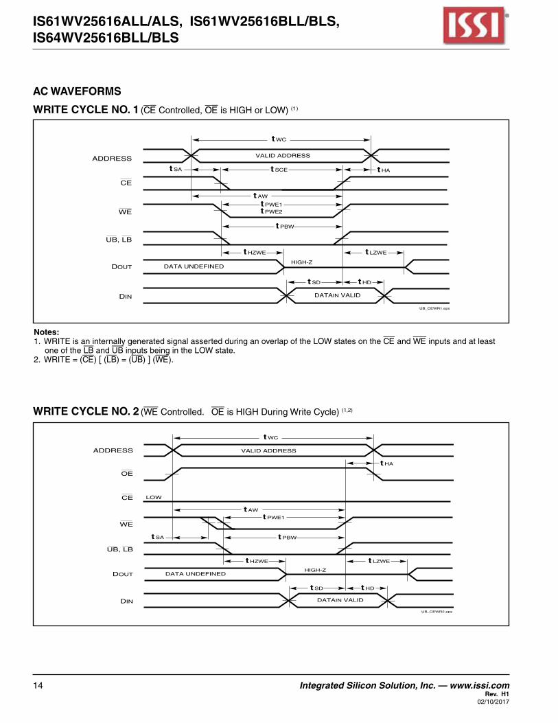
WRITE CYCLE NO. 2 (WE Controlled. OE is HIGH During Write Cycle) (1,2)
DATA UNDEFINED
LOW
t WC
VALID ADDRESS
t PWE1
t AW
t HA
HIGH-Z
t PBW
t HD
t SA
t HZWE
ADDRESS
CE
UB, LB
WE
DOUT
DIN
OE
DATAIN VALID
t LZWE
t SD
UB_CEWR2.eps
Notes: 1. WRITEisaninternallygeneratedsignalassertedduringanoverlapoftheLOWstatesontheCE and WE inputs and at least
one of the LB and UB inputs being in the LOW state.2. WRITE=(CE) [ (LB) = (UB) ] (WE).
AC WAVEFORMS
WRITE CYCLE NO. 1 (CE Controlled, OE is HIGH or LOW) (1 )
DATA UNDEFINED
t WC
VALID ADDRESS
t SCE
t PWE1t PWE2
t AW
t HA
HIGH-Z
t PBW
t HD
t SA
t HZWE
ADDRESS
CE
UB, LB
WE
DOUT
DIN DATAIN VALID
t LZWE
t SD
UB_CEWR1.eps
Integrated Silicon Solution, Inc. — www.issi.com 15Rev. H102/10/2017
IS61WV25616ALL/ALS, IS61WV25616BLL/BLS, IS64WV25616BLL/BLS
AC WAVEFORMS
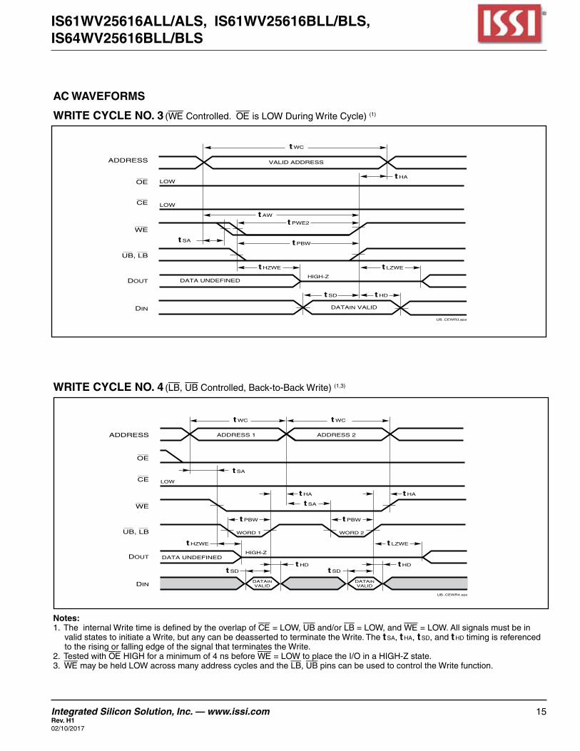
WRITE CYCLE NO. 3 (WE Controlled. OE is LOW During Write Cycle) (1)
DATA UNDEFINED
t WC
VALID ADDRESS
LOW
LOW
t PWE2
t AW
t HA
HIGH-Z
t PBW
t HD
t SA
t HZWE
ADDRESS
CE
UB, LB
WE
DOUT
DIN
OE
DATAIN VALID
t LZWE
t SD
UB_CEWR3.eps
WRITE CYCLE NO. 4 (LB, UB Controlled, Back-to-Back Write) (1,3)
DATA UNDEFINED
t WC
ADDRESS 1 ADDRESS 2
t WC
HIGH-Z
t PBW
WORD 1
LOW
WORD 2
UB_CEWR4.eps
t HD
t SA
t HZWE
ADDRESS
CE
UB, LB
WE
DOUT
DIN
OE
DATAINVALID
t LZWE
t SD
t PBW
DATAINVALID
t SDt HD
t SA
t HA t HA
Notes: 1. TheinternalWritetimeisdefinedbytheoverlapofCE = Low, UB and/or LB = Low, and WE = LOW. All signals must be in
validstatestoinitiateaWrite,butanycanbedeassertedtoterminatetheWrite.Thet sA, t HA, t sd, and t Hd timing is referenced to the rising or falling edge of the signal that terminates the Write.
2. TestedwithOE HIGH for a minimum of 4 ns before WE = LOW to place the I/O in a HIGH-Z state.3. WE may be held LOW across many address cycles and the LB, UB pins can be used to control the Write function.
16 Integrated Silicon Solution, Inc. — www.issi.comRev. H1
02/10/2017
IS61WV25616ALL/ALS, IS61WV25616BLL/BLS, IS64WV25616BLL/BLS
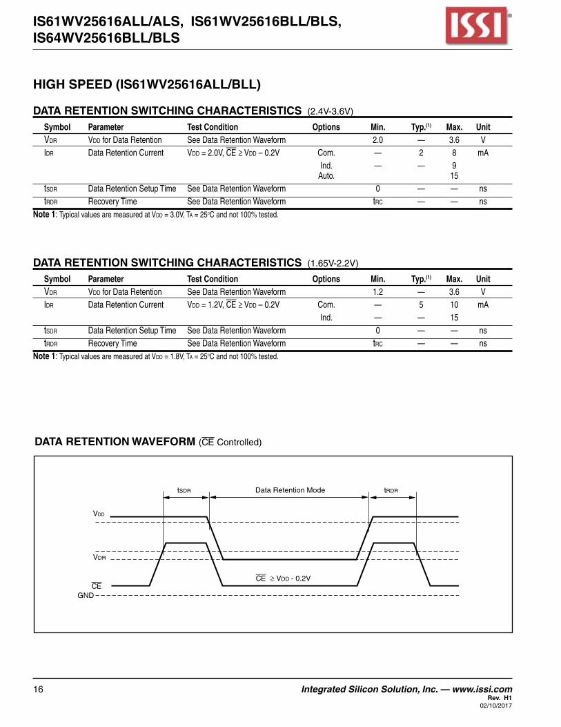
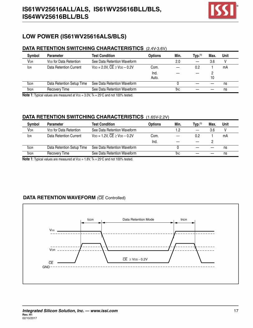
DATA RETENTION WAVEFORM (CE Controlled)
HIGH SPEED (IS61WV25616ALL/BLL)
DATA RETENTION SWITCHING CHARACTERISTICS (2.4V-3.6V)
Symbol Parameter Test Condition Options Min. Typ.(1) Max. Unit Vdr VddforDataRetention SeeDataRetentionWaveform 2.0 — 3.6 V Idr Data Retention Current Vdd = 2.0V, CE ≥ Vdd–0.2V Com. — 2 8 mA Ind. — — 9 Auto. 15 tsdr DataRetentionSetupTime SeeDataRetentionWaveform 0 — — ns trdr RecoveryTime SeeDataRetentionWaveform trc — — nsNote 1: TypicalvaluesaremeasuredatVdd=3.0V,TA = 25oc and not 100% tested.
VDD
CE ≥ VDD - 0.2V
tSDR tRDR
VDR
CEGND
Data Retention Mode
DATA RETENTION SWITCHING CHARACTERISTICS (1.65V-2.2V)
Symbol Parameter Test Condition Options Min. Typ.(1) Max. Unit Vdr VddforDataRetention SeeDataRetentionWaveform 1.2 — 3.6 V Idr Data Retention Current Vdd = 1.2V, CE ≥ Vdd – 0.2V Com. — 5 10 mA Ind. — — 15 tsdr DataRetentionSetupTime SeeDataRetentionWaveform 0 — — ns trdr RecoveryTime SeeDataRetentionWaveform trc — — nsNote 1: TypicalvaluesaremeasuredatVdd=1.8V,TA = 25oc and not 100% tested.
Integrated Silicon Solution, Inc. — www.issi.com 17Rev. H102/10/2017
IS61WV25616ALL/ALS, IS61WV25616BLL/BLS, IS64WV25616BLL/BLS
DATA RETENTION WAVEFORM (CE Controlled)
LOW POWER (IS61WV25616ALS/BLS)
DATA RETENTION SWITCHING CHARACTERISTICS (2.4V-3.6V)
Symbol Parameter Test Condition Options Min. Typ.(1) Max. Unit Vdr VddforDataRetention SeeDataRetentionWaveform 2.0 — 3.6 V Idr Data Retention Current Vdd = 2.0V, CE ≥ Vdd – 0.2V Com. — 0.2 1 mA Ind. — — 2 Auto. 10 tsdr DataRetentionSetupTime SeeDataRetentionWaveform 0 — — ns trdr RecoveryTime SeeDataRetentionWaveform trc — — nsNote 1: TypicalvaluesaremeasuredatVdd=3.0V,TA = 25oc and not 100% tested.
VDD
CE ≥ VDD - 0.2V
tSDR tRDR
VDR
CEGND
Data Retention Mode
DATA RETENTION SWITCHING CHARACTERISTICS (1.65V-2.2V)
Symbol Parameter Test Condition Options Min. Typ.(1) Max. Unit Vdr VddforDataRetention SeeDataRetentionWaveform 1.2 — 3.6 V Idr Data Retention Current Vdd = 1.2V, CE ≥ Vdd – 0.2V Com. — 0.2 1 mA Ind. — — 2 tsdr DataRetentionSetupTime SeeDataRetentionWaveform 0 — — ns trdr RecoveryTime SeeDataRetentionWaveform trc — — nsNote 1: TypicalvaluesaremeasuredatVdd=1.8V,TA = 25oc and not 100% tested.
18 Integrated Silicon Solution, Inc. — www.issi.comRev. H1
02/10/2017
IS61WV25616ALL/ALS, IS61WV25616BLL/BLS, IS64WV25616BLL/BLS
ORDERING INFORMATION (HIGH SPEED)
Commercial Range: 0°C to +70°CVoltage Range: 2.4V to 3.6V Speed (ns) Order Part No. Package
10(81) IS61WV25616BLL-10TL TSOP(TypeII),Lead-free Note:1.Speed=8nsforVdd=3.3V+ 5%. Speed = 10ns for Vdd=2.4Vto3.6V.
Industrial Range: -40°C to +85°CVoltage Range: 2.4V to 3.6V Speed (ns) Order Part No. Package
10(81) IS61WV25616BLL-10BI 48miniBGA(6mmx8mm) IS61WV25616BLL-10BLI 48miniBGA(6mmx8mm),Lead-free IS61WV25616BLL-10TI TSOP(TypeII) IS61WV25616BLL-10TLI TSOP(TypeII),Lead-free
IS61WV25616BLL-10KLI 400-mil SOJ, Lead-freeNote:1.Speed=8nsforVdd=3.3V+ 5%. Speed = 10ns for Vdd=2.4Vto3.6V.
Industrial Range: -40°C to +85°CVoltage Range: 1.65V to 2.2V
Speed (ns) Order Part No. Package
20 IS61WV25616ALL-20BI 48miniBGA(6mmx8mm) IS61WV25616ALL-20TI TSOP(TypeII) IS61WV25616ALL-20TLI TSOP(TypeII),Lead-free
Automotive Range: -40°C to +125°CVoltage Range: 2.4V to 3.6V
Speed (ns) Order Part No. Package
10 IS64WV25616BLL-10BA3 48miniBGA(6mmx8mm) IS64WV25616BLL-10BLA3 48miniBGA(6mmx8mm),Lead-free IS64WV25616BLL-10CTA3 TSOP(TypeII),CopperLeadframe IS64WV25616BLL-10CTLA3 TSOP(TypeII),Lead-free,CopperLeadframe
Integrated Silicon Solution, Inc. — www.issi.com 19Rev. H102/10/2017
IS61WV25616ALL/ALS, IS61WV25616BLL/BLS, IS64WV25616BLL/BLS
ORDERING INFORMATION (LOW POWER)
Industrial Range: -40°C to +85°CVoltage Range: 2.4V to 3.6V
Speed (ns) Order Part No. Package
25 IS61WV25616BLS-25TLI TSOP(TypeII),Lead-free
Industrial Range: -40°C to +85°CVoltage Range: 1.65V to 2.2V
Speed (ns) Order Part No. Package
45 IS61WV25616ALS-45TLI TSOP(TypeII),Lead-free
20 Integrated Silicon Solution, Inc. — www.issi.comRev. H1
02/10/2017
IS61WV25616ALL/ALS, IS61WV25616BLL/BLS, IS64WV25616BLL/BLS
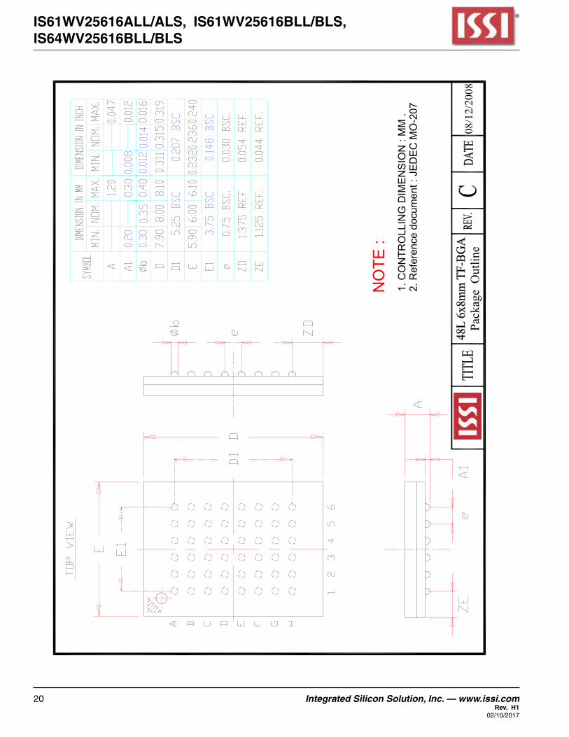
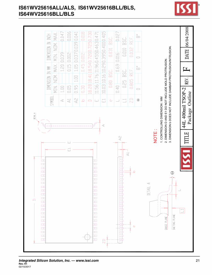
2. R
efer
ence
doc
umen
t : J
ED
EC
MO
-207
1. C
ON
TRO
LLIN
G D
IME
NS
ION
: M
M .
NO
TE :
08/1
2/20
08Pa
ckag
e O
utlin
e
Integrated Silicon Solution, Inc. — www.issi.com 21Rev. H102/10/2017
IS61WV25616ALL/ALS, IS61WV25616BLL/BLS, IS64WV25616BLL/BLS
2. D
IMEN
SIO
N D
AN
D E
1 D
O N
OT
INC
LUD
E M
OLD
PR
OTR
USI
ON
.3.
DIM
EN
SIO
N b
DO
ES
NO
T IN
CLU
DE
DA
MB
AR
PR
OTR
US
ION
/INTR
US
ION
.
1. C
ON
TRO
LLIN
G D
IME
NS
ION
: M
M
NO
TE :
06/0
4/20
08Pa
ckag
e O
utlin
e
22 Integrated Silicon Solution, Inc. — www.issi.comRev. H1
02/10/2017
IS61WV25616ALL/ALS, IS61WV25616BLL/BLS, IS64WV25616BLL/BLS
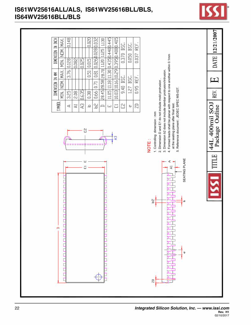
3. D
imen
sion
b2
does
not
incl
ude
dam
bar p
rotru
sion
/intru
sion
.4.
For
med
lead
s sh
all b
e pl
anar
with
resp
ect t
o on
e an
othe
r with
in 0
.1m
m
2. D
imen
sion
D a
nd E
1 do
not
incl
ude
mol
d pr
otru
sion
.
at t
he s
eatin
g pl
ane
afte
r fin
al te
st.
1. C
ontro
lling
dim
ensi
on :
mm
NO
TE :
SE
ATI
NG
PLA
NE
5. R
efer
ence
doc
umen
t : J
ED
EC
SP
EC
MS
-027
.
12/2
1/20
07